US20040225377A1 - Method, system and medium for controlling manufacture process having multivariate input parameters - Google Patents
Method, system and medium for controlling manufacture process having multivariate input parametersDownload PDFInfo
- Publication number
- US20040225377A1 US20040225377A1US10/712,273US71227303AUS2004225377A1US 20040225377 A1US20040225377 A1US 20040225377A1US 71227303 AUS71227303 AUS 71227303AUS 2004225377 A1US2004225377 A1US 2004225377A1
- Authority
- US
- United States
- Prior art keywords
- right arrow
- arrow over
- values
- coefficients
- calculating
- Prior art date
- Legal status (The legal status is an assumption and is not a legal conclusion. Google has not performed a legal analysis and makes no representation as to the accuracy of the status listed.)
- Granted
Links
- 238000000034methodMethods0.000titleclaimsabstractdescription34
- 238000004519manufacturing processMethods0.000titleclaimsabstractdescription16
- 230000008569processEffects0.000titledescription8
- 230000008859changeEffects0.000claimsabstractdescription10
- 230000009466transformationEffects0.000claimsdescription15
- 230000001131transforming effectEffects0.000abstractdescription2
- 238000012545processingMethods0.000description21
- 230000006870functionEffects0.000description13
- 235000012431wafersNutrition0.000description10
- 238000010586diagramMethods0.000description8
- 238000004891communicationMethods0.000description5
- 239000002609mediumSubstances0.000description5
- 239000004065semiconductorSubstances0.000description3
- 238000004364calculation methodMethods0.000description2
- 238000007796conventional methodMethods0.000description2
- 230000008021depositionEffects0.000description2
- 230000000694effectsEffects0.000description2
- 238000012986modificationMethods0.000description2
- 230000004048modificationEffects0.000description2
- 230000003287optical effectEffects0.000description2
- 238000005498polishingMethods0.000description2
- XUIMIQQOPSSXEZ-UHFFFAOYSA-NSiliconChemical compound[Si]XUIMIQQOPSSXEZ-UHFFFAOYSA-N0.000description1
- 230000003044adaptive effectEffects0.000description1
- 238000004590computer programMethods0.000description1
- 239000004020conductorSubstances0.000description1
- 238000010276constructionMethods0.000description1
- 238000012937correctionMethods0.000description1
- 238000013178mathematical modelMethods0.000description1
- 238000004377microelectronicMethods0.000description1
- 238000012544monitoring processMethods0.000description1
- 239000013307optical fiberSubstances0.000description1
- 230000002093peripheral effectEffects0.000description1
- 230000008054signal transmissionEffects0.000description1
- 229910052710siliconInorganic materials0.000description1
- 239000010703siliconSubstances0.000description1
- 239000000126substanceSubstances0.000description1
- 239000000758substrateSubstances0.000description1
- 238000000844transformationMethods0.000description1
- 239000006163transport mediaSubstances0.000description1
- 230000000007visual effectEffects0.000description1
Images


Classifications
- G—PHYSICS
- G05—CONTROLLING; REGULATING
- G05B—CONTROL OR REGULATING SYSTEMS IN GENERAL; FUNCTIONAL ELEMENTS OF SUCH SYSTEMS; MONITORING OR TESTING ARRANGEMENTS FOR SUCH SYSTEMS OR ELEMENTS
- G05B11/00—Automatic controllers
- G05B11/01—Automatic controllers electric
- G05B11/32—Automatic controllers electric with inputs from more than one sensing element; with outputs to more than one correcting element
- G—PHYSICS
- G05—CONTROLLING; REGULATING
- G05B—CONTROL OR REGULATING SYSTEMS IN GENERAL; FUNCTIONAL ELEMENTS OF SUCH SYSTEMS; MONITORING OR TESTING ARRANGEMENTS FOR SUCH SYSTEMS OR ELEMENTS
- G05B13/00—Adaptive control systems, i.e. systems automatically adjusting themselves to have a performance which is optimum according to some preassigned criterion
- G05B13/02—Adaptive control systems, i.e. systems automatically adjusting themselves to have a performance which is optimum according to some preassigned criterion electric
- G05B13/04—Adaptive control systems, i.e. systems automatically adjusting themselves to have a performance which is optimum according to some preassigned criterion electric involving the use of models or simulators
- G05B13/042—Adaptive control systems, i.e. systems automatically adjusting themselves to have a performance which is optimum according to some preassigned criterion electric involving the use of models or simulators in which a parameter or coefficient is automatically adjusted to optimise the performance
- G—PHYSICS
- G05—CONTROLLING; REGULATING
- G05B—CONTROL OR REGULATING SYSTEMS IN GENERAL; FUNCTIONAL ELEMENTS OF SUCH SYSTEMS; MONITORING OR TESTING ARRANGEMENTS FOR SUCH SYSTEMS OR ELEMENTS
- G05B13/00—Adaptive control systems, i.e. systems automatically adjusting themselves to have a performance which is optimum according to some preassigned criterion
- G05B13/02—Adaptive control systems, i.e. systems automatically adjusting themselves to have a performance which is optimum according to some preassigned criterion electric
- G05B13/04—Adaptive control systems, i.e. systems automatically adjusting themselves to have a performance which is optimum according to some preassigned criterion electric involving the use of models or simulators
- G05B13/048—Adaptive control systems, i.e. systems automatically adjusting themselves to have a performance which is optimum according to some preassigned criterion electric involving the use of models or simulators using a predictor
- Y—GENERAL TAGGING OF NEW TECHNOLOGICAL DEVELOPMENTS; GENERAL TAGGING OF CROSS-SECTIONAL TECHNOLOGIES SPANNING OVER SEVERAL SECTIONS OF THE IPC; TECHNICAL SUBJECTS COVERED BY FORMER USPC CROSS-REFERENCE ART COLLECTIONS [XRACs] AND DIGESTS
- Y02—TECHNOLOGIES OR APPLICATIONS FOR MITIGATION OR ADAPTATION AGAINST CLIMATE CHANGE
- Y02P—CLIMATE CHANGE MITIGATION TECHNOLOGIES IN THE PRODUCTION OR PROCESSING OF GOODS
- Y02P90/00—Enabling technologies with a potential contribution to greenhouse gas [GHG] emissions mitigation
- Y02P90/02—Total factory control, e.g. smart factories, flexible manufacturing systems [FMS] or integrated manufacturing systems [IMS]
Definitions
- the present inventionrelates to a method, system and medium for modeling and controlling processes. More specifically, the present invention relates to modeling and controlling semiconductor-processing equipment that has multivariate input parameters.
- controlling manufacturing processesplays a crucial role. Controlling such processes may require, among other things, monitoring the characteristics of manufactured parts (e.g., processed wafers, hereinafter referred to as outputs) and adjusting input parameters accordingly. By adjusting the values of the input parameters, different types of outputs can be produced and the characteristics of the outputs can also be controlled.
- a mathematical model of the processing equipmentcan be used.
- One example of such a modelis called a predictive model. This model is used to predict the future output values (e.g., the characteristics of products) based on historical information (e.g., input parameter values and the corresponding output qualities).
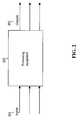
- One such predictive modelis an offset technique, which is illustrated in FIG. 1.
- the values of a number of input parameters 101are received by an input/output dependency model 103 , which calculates a predicted output value y 1 Pred 105 based on the input values.
- a corrector 109then compares the predicted value y 1 Pred with an actual output value y 1 a 107 for the given values of the input parameters. If the predicted and actual output values are similar to each other within a certain range, no change is made to the input/output dependency model 103 . If the predicted and actual output values are different (e.g., outside the range) from each other, the predictor input/output dependency model 103 is modified by adjusting an offset value (O 1 ) 111 based on the magnitude of the difference.
- At least some of the outputsmay include mutual (shared) inputs. This means the output values of the equipment are not completely independent from each other (e.g., changing an input to adjust a given output may unintentionally change the characteristics of other outputs).
- each outputhas its own correction system as if the output values are independent from each other. Because the dependencies between the different outputs are not accounted for by the conventional technique, it does not always lead to accurate predictions. In addition, adjusting one offset of one output can affect other outputs.
- Embodiments of the present inventionadvantageously overcome the above-described shortcomings of the aforementioned techniques. More specifically, embodiments of the present invention provide a system, method and medium for controlling semiconductor-processing equipment that has multivariate input parameters and outputs.
- Embodiments of the present inventionminimize the effects of outputs being interdependent from each other. This is achieved by providing input parameter transformations having transformation coefficients. The coefficients are obtained by minimizing a score function. This, in turn, allows accurate models to be obtained. Using the models, highly precise control of manufacturing equipment is accomplished.
- an example methodincludes the steps of identifying at least one input that causes a change in at least two of a plurality of outputs, storing values of the identified inputs and corresponding empirical output values, and calculating and storing predicted output values, based on, in part, the values of the identified inputs.
- the example methodmay further include the steps of calculating a set of transform coefficients by minimizing a score equation that is a function of, in part, differences between one or more of the empirical output values and their corresponding predicted output values, and calculating one or more input values for one or more desired output values based on, in part, the calculated set of transform coefficients.
- FIG. 1is a diagram showing a conventional offset model
- FIG. 2is a diagram illustrating processing equipment
- FIG. 3is a diagram illustrating a model of the processing equipment shown in FIG. 2 in accordance with embodiments of the present invention
- FIG. 4is a block diagram illustrating various components of embodiments of the present invention.
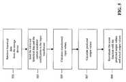
- FIG. 5is a flow chart illustrating processing steps of embodiments of the present invention.
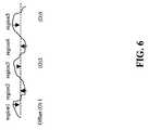
- FIG. 6is a diagram illustrating a CMP process
- FIG. 7is a block diagram representation of an example embodiment of a computer configured to perform embodiments of the present invention.
- FIG. 8is a diagram illustrating an example of a memory medium that can be used for storing computer programs of embodiments of the present invention.
- Embodiments of the present inventiongenerally provide systems, methods and mediums for creating one or more adaptive process models to mathematically represent multivariate input parameter systems.
- the present inventionis particularly applicable in a manufacturing process such as manufacturing and/or processing semiconductor wafers.
- the present inventionrelates to modeling techniques as used by equipment involved in the manufacturing of semiconductor wafers.
- a general overview of embodiments of the present inventionis provided below. It will be followed by a specific example implementation of the present invention.
- FIG. 2shows a simplified graphical representation of processing equipment 205 with input parameters 201 and outputs 203 .
- processing equipmentinclude etcher tools, deposition tools, chemical mechanical planarization (CMP) tools, etc.
- the processing equipment 205can include one or more tools.
- different processescan be achieved. For instance, in a deposition tool, different types of layers can be deposited on a wafer and/or the thickness of the layer can be varied.
- the processing equipment 205has a set of input parameters 301 , a set of predicted outputs 303 , and a prediction model 305 therebetween (replacing the processing equipment of FIG. 2).
- the overall goal of the prediction modelis to minimize differences between the predicted output values and empirically collected output values (i.e., the actual output values).
- the modelcan then be used in setting input parameters based on desired output values. In other words, for a given set of desired output values, the model can be used in a reverse fashion to calculate the input parameter values that would cause output values close to the desired output values.
- the calculated input parameter valuesare also known as recipes.
- the step of obtaining the predictive modelcan be divided into two steps. The first is to transform the values of the input parameters 301 into transformed input values 307 . The second is to use the transformed input values 307 in calculating predicted output values 303 .
- X′ 1P 11 X 1 +P 12 X 1 2 ;
- X′ 2P 21 X 1 +P 22 X 2 2 +P cross X 1 X 2 (In this example, P 11 , P 12 , P 21 , P 22 and P cross can have different values.)
- the coefficient valuesare calculated by the steps of: a. collecting historical information on input parameter values and actual output values; b. creating a score function based on the collected information; and c. finding the coefficient values that minimize the score function, S p .
- the step of collecting the historical informationentails a set of data points for processing a number of wafers.
- input parameter values and actual output values for a number of wafers that have been processed by the processing equipmentwould be collected. This collection would then be used in the next step of minimizing the score function.
- y predicteda predicted output value, as calculated based on transformed inputs for a particular wafer i ( ⁇ right arrow over (X) ⁇ ′i );
- This calculationis performed using the following transformation functions:
- the next stepis to minimize the score S p , i.e., to find ⁇ right arrow over (P) ⁇ values that provide the minimum of S p ⁇ ( S p ⁇ ⁇ p ⁇ min )
- the above-described stepscalculate an optimal ⁇ right arrow over (P) ⁇ (i.e., a vector of coefficients for input transformation functions) such that the prediction model of the present invention provides the closest possible predicted outputs to the actual outputs.
- P⁇ right arrow over
- the example implementationincludes a number of components: an input transformer 401 , an input-output dependency model 403 , a corrector 405 and a storage device 407 . All these components can be implemented in hardware, firmware, software and/or any combination thereof.
- the historical information(i.e., y a ik , ⁇ right arrow over (X) ⁇ i ) is stored into the storage device 407 .
- the corrector 405then retrieves the historical information (y a ik , ⁇ right arrow over (X) ⁇ i ) from the storage device 407 (step 501 ). Since the retrieved historical information contains raw input parameter values, the information is sent to the input transformer 401 along with coefficients ⁇ right arrow over (P) ⁇ (step 503 ).
- the coefficient ⁇ right arrow over (P) ⁇can be stored in the storage device 407 or in the corrector 405 .
- the input transformer 401upon receiving the information from the corrector 405 , calculates transformed input parameter values ⁇ right arrow over (X) ⁇ ′i (step 505 ). Once the transformed input parameter values are calculated, the input transformer 401 sends the transformed input values to the corrector 405 .
- the corrector 405upon receiving the transformed input parameter values from the input transformer 401 , sends the transformed input parameter values to the input/output dependence model 403 .
- the input/output dependency model 403then calculates predicted output parameter values y pred (step 507 ).
- the corrector 405then calculates the score S p , and sets a new ⁇ right arrow over (P) ⁇ (a vector of parameters of input transformation functions) in order to minimize the score S p (step 509 ). These steps can be repeated until an optimum ⁇ right arrow over (P) ⁇ that yields a minimal score S p is obtained, and return the optimum ⁇ right arrow over (P) ⁇ .
- the optimum coefficientscan be combined with the most recent vector such that: ⁇ right arrow over (P) ⁇ new ⁇ right arrow over (P) ⁇ previous +K( ⁇ right arrow over (P) ⁇ optimum — ⁇ right arrow over (P) ⁇ previous ) wherein K ⁇ 1.
- a set of input valuescan be obtained (e.g., a recipe) for a desired set of output values. More specifically, from a set of desired values, a set of transformed input values, ⁇ right arrow over (X) ⁇ ′i , can be obtained by reversing the predictive model (e.g., the input/output dependence model 403 ). The transformed input values can then be reverse transformed using the coefficients ⁇ right arrow over (P) ⁇ to obtain the input value to produce the desired output values.
- the predictive modele.g., the input/output dependence model 403
- the raw input valuesare transformed using the calculated coefficients.
- the transformationis required to account for the dependencies among input parameters as graphically illustrated in FIG. 6. More specifically, a surface of a wafer having five regions with varying degrees of roughness is to be polished by a CMP process. The goal is to achieve a flat surface depicted by a dotted line in FIG. 6.
- one regionwould be polished without regard to the other regions.
- polishing one regioncan affect the polishing of another region (e.g., when an offset is applied in region 1 in order to bring the height in region 1 down to the broken line, the height in region 2 is also influenced by the changes of region 1 ). Using the embodiments of the present invention, these dependencies are accounted for.
- FIG. 7illustrates a block diagram of one example of the internal hardware 713 of a computer configured to perform embodiments of the present invention.
- a bus 756serves as the main information highway interconnecting various components therein.
- CPU 758is the central processing unit of the internal hardware 713 , performing calculations and logic operations required to execute embodiments of the present invention as well as other programs.
- Read only memory (ROM) 760 and random access memory (RAM) 762constitute the main memory.
- Disk controller 764interfaces one or more disk drives to the system bus 756 . These disk drives are, for example, floppy disk drives 770 , or CD ROM or DVD (digital video disks) drives 766 , or internal or external hard drives 768 . These various disk drives and disk controllers are optional devices.
- a display interface 772interfaces display 748 and permits information from the bus 756 to be displayed on display 748 .
- Optical fibers and/or electrical cables and/or conductors and/or optical communication (e.g., infrared, and the like) and/or wireless communication (e.g., radio frequency (RF), and the like)can be used as the transport medium between the external devices and communication port 774 .
- Peripheral interface 754interfaces the keyboard 750 and mouse 752 , permitting input data to be transmitted to bus 756 .
- the internal hardware 713also optionally includes an infrared transmitter and/or infrared receiver.
- Infrared transmittersare optionally utilized when the computer system is used in conjunction with one or more of the processing components/stations/modules that transmit/receive data via infrared signal transmission.
- the computer systemmay also optionally use a low power radio transmitter 780 and/or a low power radio receiver 782 .
- the low power radio transmittertransmits the signal for reception by components of the production process, and receives signals from the components via the low power radio receiver.
- the low power radio transmitter and/or receiverare standard devices in industry.
- the computer in FIG. 7is illustrated having a single processor, a single hard disk drive and a single local memory
- the analyzeris optionally suitably equipped with any multitude or combination of processors or storage devices.
- the computermay be replaced by, or combined with, any suitable processing system operative in accordance with the principles of embodiments of the present invention, including sophisticated calculators, and hand-held, laptop/notebook, mini, mainframe and super computers, as well as processing system network combinations of the same.
- FIG. 8is an illustration of an example computer readable memory medium 884 utilizable for storing computer readable code or instructions.
- medium 884may be used with disk drives illustrated in FIG. 7.
- memory mediasuch as floppy disks, or a CD ROM, or a digital video disk will contain, for example, a multi-byte locale for a single byte language and the program information for controlling the modeler to enable the computer to perform the functions described herein.
- ROM 760 and/or RAM 762 illustrated in FIG. 7can also be used to store the program information that is used to instruct the central processing unit 758 to perform the operations associated with various automated processes of the present invention.
- suitable computer readable media for storing informationinclude magnetic, electronic, or optical (including holographic) storage, some combination thereof, etc.
- output valuescan be transformed similar to the transform performed on the input parameters, and operations can be performed on the transformed output values similar to those performed on the transformed input parameters.
Landscapes
- Engineering & Computer Science (AREA)
- Physics & Mathematics (AREA)
- Automation & Control Theory (AREA)
- General Physics & Mathematics (AREA)
- Computer Vision & Pattern Recognition (AREA)
- Medical Informatics (AREA)
- Software Systems (AREA)
- Evolutionary Computation (AREA)
- Health & Medical Sciences (AREA)
- Artificial Intelligence (AREA)
- Drying Of Semiconductors (AREA)
- General Factory Administration (AREA)
- Testing Or Measuring Of Semiconductors Or The Like (AREA)
- Feedback Control In General (AREA)
- Testing And Monitoring For Control Systems (AREA)
Abstract
Description
- This application claims priority from U.S. Provisional Application No. 60/426,393, filed Nov. 15, 2002, which is incorporated herein by reference.[0001]
- The present invention relates to a method, system and medium for modeling and controlling processes. More specifically, the present invention relates to modeling and controlling semiconductor-processing equipment that has multivariate input parameters.[0002]
- In manufacturing products that include precision discrete parts (e.g., microelectronic chips on silicon substrates), controlling manufacturing processes plays a crucial role. Controlling such processes may require, among other things, monitoring the characteristics of manufactured parts (e.g., processed wafers, hereinafter referred to as outputs) and adjusting input parameters accordingly. By adjusting the values of the input parameters, different types of outputs can be produced and the characteristics of the outputs can also be controlled.[0003]
- For automating the control of the manufacturing processes, a mathematical model of the processing equipment can be used. One example of such a model is called a predictive model. This model is used to predict the future output values (e.g., the characteristics of products) based on historical information (e.g., input parameter values and the corresponding output qualities).[0004]
- One such predictive model is an offset technique, which is illustrated in FIG. 1. In particular, the values of a number of[0005]
input parameters 101 are received by an input/output dependency model 103, which calculates a predictedoutput value y 1Pred105 based on the input values. Acorrector 109 then compares the predicted value y1Predwith an actualoutput value y 1a107 for the given values of the input parameters. If the predicted and actual output values are similar to each other within a certain range, no change is made to the input/output dependency model 103. If the predicted and actual output values are different (e.g., outside the range) from each other, the predictor input/output dependency model 103 is modified by adjusting an offset value (O1)111 based on the magnitude of the difference. - In equipment that has more than one output, at least some of the outputs may include mutual (shared) inputs. This means the output values of the equipment are not completely independent from each other (e.g., changing an input to adjust a given output may unintentionally change the characteristics of other outputs). In a conventional modeling technique, each output has its own correction system as if the output values are independent from each other. Because the dependencies between the different outputs are not accounted for by the conventional technique, it does not always lead to accurate predictions. In addition, adjusting one offset of one output can affect other outputs.[0006]
- Embodiments of the present invention advantageously overcome the above-described shortcomings of the aforementioned techniques. More specifically, embodiments of the present invention provide a system, method and medium for controlling semiconductor-processing equipment that has multivariate input parameters and outputs.[0007]
- Embodiments of the present invention minimize the effects of outputs being interdependent from each other. This is achieved by providing input parameter transformations having transformation coefficients. The coefficients are obtained by minimizing a score function. This, in turn, allows accurate models to be obtained. Using the models, highly precise control of manufacturing equipment is accomplished.[0008]
- In particular, an example method according to embodiments of the present invention includes the steps of identifying at least one input that causes a change in at least two of a plurality of outputs, storing values of the identified inputs and corresponding empirical output values, and calculating and storing predicted output values, based on, in part, the values of the identified inputs. The example method may further include the steps of calculating a set of transform coefficients by minimizing a score equation that is a function of, in part, differences between one or more of the empirical output values and their corresponding predicted output values, and calculating one or more input values for one or more desired output values based on, in part, the calculated set of transform coefficients.[0009]
- The detailed description of the present application showing various distinctive features may be best understood when the detailed description is read in reference to the appended drawings in which:[0010]
- FIG. 1 is a diagram showing a conventional offset model;[0011]
- FIG. 2 is a diagram illustrating processing equipment;[0012]
- FIG. 3 is a diagram illustrating a model of the processing equipment shown in FIG. 2 in accordance with embodiments of the present invention;[0013]
- FIG. 4 is a block diagram illustrating various components of embodiments of the present invention[0014]
- FIG. 5 is a flow chart illustrating processing steps of embodiments of the present invention;[0015]
- FIG. 6 is a diagram illustrating a CMP process;[0016]
- FIG. 7 is a block diagram representation of an example embodiment of a computer configured to perform embodiments of the present invention; and[0017]
- FIG. 8 is a diagram illustrating an example of a memory medium that can be used for storing computer programs of embodiments of the present invention.[0018]
- Embodiments of the present invention generally provide systems, methods and mediums for creating one or more adaptive process models to mathematically represent multivariate input parameter systems. The present invention is particularly applicable in a manufacturing process such as manufacturing and/or processing semiconductor wafers. In particular, the present invention relates to modeling techniques as used by equipment involved in the manufacturing of semiconductor wafers. A general overview of embodiments of the present invention is provided below. It will be followed by a specific example implementation of the present invention.[0019]
- Before discussing embodiments of the present invention, FIG. 2 shows a simplified graphical representation of[0020]
processing equipment 205 withinput parameters 201 andoutputs 203. Examples of processing equipment include etcher tools, deposition tools, chemical mechanical planarization (CMP) tools, etc. Theprocessing equipment 205 can include one or more tools. Depending upon the values of theinput parameters 201, different processes can be achieved. For instance, in a deposition tool, different types of layers can be deposited on a wafer and/or the thickness of the layer can be varied. - As a general overview of embodiments of the present invention, in FIG. 3, the[0021]
processing equipment 205 has a set ofinput parameters 301, a set of predictedoutputs 303, and aprediction model 305 therebetween (replacing the processing equipment of FIG. 2). The overall goal of the prediction model is to minimize differences between the predicted output values and empirically collected output values (i.e., the actual output values). Once the prediction model is optimized (e.g., the differences between the predicted and actual output values have been minimized), the model can then be used in setting input parameters based on desired output values. In other words, for a given set of desired output values, the model can be used in a reverse fashion to calculate the input parameter values that would cause output values close to the desired output values. The calculated input parameter values are also known as recipes. - In embodiments of the present invention, the step of obtaining the predictive model can be divided into two steps. The first is to transform the values of the[0022]
input parameters 301 intotransformed input values 307. The second is to use thetransformed input values 307 in calculating predictedoutput values 303. - With respect to the transformation, input parameter values (X[0023]1, X2, X3) along with coefficient vector {right arrow over (P)} are transformed into (X′1, X′2, and X′3) by transform functions ψ1ψ2, and ψ3. Examples of transformation functions include:
- 1) X′[0024]1=PX1; X′2=PX2(In this example, the value of {right arrow over (P)} is identical for both X1 and X2.)
- 2) X′[0025]1=P11X1+P12X12; X′2=P21X1+P22X22+PcrossX1X2(In this example, P11, P12, P21, P22and Pcrosscan have different values.)
- The coefficient values are calculated by the steps of: a. collecting historical information on input parameter values and actual output values; b. creating a score function based on the collected information; and c. finding the coefficient values that minimize the score function, S[0026]p.
- The above steps are described by making references to semiconductor processing tools. As such, the step of collecting the historical information entails a set of data points for processing a number of wafers. In particular, input parameter values and actual output values for a number of wafers that have been processed by the processing equipment would be collected. This collection would then be used in the next step of minimizing the score function.[0027]
- where:[0029]
- i—number of wafer;[0030]
- k—number of output;[0031]
- y[0032]actual—an actual output value;
- y[0033]predicted—a predicted output value, as calculated based on transformed inputs for a particular wafer i ({right arrow over (X)}′i);
- {right arrow over (X)}[0034]′i=(X140 i,X240 i,X3′i) is the transformed input vector, calculated on the base of the actual input; and {right arrow over (X)}i=(X1i, X2i,X3i) for wafer i together with the transformation parameters {right arrow over (P)}. This calculation is performed using the following transformation functions:
- ψ1(X1,X2,X3,{right arrow over (P)}): ψ2(X1,X2,X3,{right arrow over (P)}); and ψ3(X1,X2,X3,{right arrow over (P)}).
- The above-described steps calculate an optimal {right arrow over (P)} (i.e., a vector of coefficients for input transformation functions) such that the prediction model of the present invention provides the closest possible predicted outputs to the actual outputs. In a processing model with multivariate input parameters, when the score is minimized, the negative effect of the interdependencies between output values on the model accuracy would also be minimized.[0036]
- Now turning to describe an example implementation of the embodiments described above, as shown in FIG. 4, the example implementation includes a number of components: an[0037]
input transformer 401, an input-output dependency model 403, acorrector 405 and astorage device 407. All these components can be implemented in hardware, firmware, software and/or any combination thereof. - These components are further explained by also referring to FIG. 5. In particular, the historical information (i.e., y[0038]aik,{right arrow over (X)}i) is stored into the
storage device 407. Thecorrector 405 then retrieves the historical information (yaik, {right arrow over (X)}i) from the storage device407 (step501). Since the retrieved historical information contains raw input parameter values, the information is sent to theinput transformer 401 along with coefficients {right arrow over (P)} (step503). The coefficient {right arrow over (P)} can be stored in thestorage device 407 or in thecorrector 405. - The[0039]
input transformer 401, upon receiving the information from thecorrector 405, calculates transformed input parameter values {right arrow over (X)}′i(step505). Once the transformed input parameter values are calculated, theinput transformer 401 sends the transformed input values to thecorrector 405. - The[0040]
corrector 405, upon receiving the transformed input parameter values from theinput transformer 401, sends the transformed input parameter values to the input/output dependence model 403. The input/output dependency model 403 then calculates predicted output parameter values ypred(step507). Thecorrector 405 then calculates the score Sp, and sets a new {right arrow over (P)} (a vector of parameters of input transformation functions) in order to minimize the score Sp(step509). These steps can be repeated until an optimum {right arrow over (P)} that yields a minimal score Spis obtained, and return the optimum {right arrow over (P)}. Each time new data is obtained, a new score from new data is created and a new optimum {right arrow over (P)} value is calculated. This newly calculated vector {right arrow over (P)} could be used for transforming the input values, meaning: {right arrow over (P)}new≡{right arrow over (P)}optimum. - In embodiments of the present invention, the optimum coefficients can be combined with the most recent vector such that: {right arrow over (P)}[0041]new≡{right arrow over (P)}previous+K({right arrow over (P)}optimum—{right arrow over (P)}previous) wherein K<1.
- As a new set of data points arrives, a new optimum {right arrow over (P)} can be recalculated.[0042]
- Once a set of coefficients is calculated, a set of input values can be obtained (e.g., a recipe) for a desired set of output values. More specifically, from a set of desired values, a set of transformed input values, {right arrow over (X)}[0043]′i, can be obtained by reversing the predictive model (e.g., the input/output dependence model403). The transformed input values can then be reverse transformed using the coefficients {right arrow over (P)} to obtain the input value to produce the desired output values.
- In the above-described embodiments, the raw input values are transformed using the calculated coefficients. The transformation is required to account for the dependencies among input parameters as graphically illustrated in FIG. 6. More specifically, a surface of a wafer having five regions with varying degrees of roughness is to be polished by a CMP process. The goal is to achieve a flat surface depicted by a dotted line in FIG. 6. In conventional techniques, one region would be polished without regard to the other regions. However, polishing one region can affect the polishing of another region (e.g., when an offset is applied in[0044]
region 1 in order to bring the height inregion 1 down to the broken line, the height in region2 is also influenced by the changes of region1). Using the embodiments of the present invention, these dependencies are accounted for. - An example embodiment of the computer in which embodiments of the present invention operate (e.g., the various components described in FIG. 4) is described below in connection with FIGS. 7-8. FIG. 7 illustrates a block diagram of one example of the[0045]
internal hardware 713 of a computer configured to perform embodiments of the present invention. Abus 756 serves as the main information highway interconnecting various components therein. CPU758 is the central processing unit of theinternal hardware 713, performing calculations and logic operations required to execute embodiments of the present invention as well as other programs. Read only memory (ROM)760 and random access memory (RAM)762 constitute the main memory.Disk controller 764 interfaces one or more disk drives to thesystem bus 756. These disk drives are, for example, floppy disk drives770, or CD ROM or DVD (digital video disks) drives766, or internal or external hard drives768. These various disk drives and disk controllers are optional devices. - A[0046]
display interface 772 interfaces display748 and permits information from thebus 756 to be displayed on display748. Communications with external devices, such as the other components of the system described above, occur utilizing, for example, communication port774. Optical fibers and/or electrical cables and/or conductors and/or optical communication (e.g., infrared, and the like) and/or wireless communication (e.g., radio frequency (RF), and the like) can be used as the transport medium between the external devices and communication port774. Peripheral interface754 interfaces thekeyboard 750 andmouse 752, permitting input data to be transmitted tobus 756. In addition to these components, theinternal hardware 713 also optionally includes an infrared transmitter and/or infrared receiver. Infrared transmitters are optionally utilized when the computer system is used in conjunction with one or more of the processing components/stations/modules that transmit/receive data via infrared signal transmission. Instead of utilizing an infrared transmitter or infrared receiver, the computer system may also optionally use a lowpower radio transmitter 780 and/or a low power radio receiver782. The low power radio transmitter transmits the signal for reception by components of the production process, and receives signals from the components via the low power radio receiver. The low power radio transmitter and/or receiver are standard devices in industry. - Although the computer in FIG. 7 is illustrated having a single processor, a single hard disk drive and a single local memory, the analyzer is optionally suitably equipped with any multitude or combination of processors or storage devices. For example, the computer may be replaced by, or combined with, any suitable processing system operative in accordance with the principles of embodiments of the present invention, including sophisticated calculators, and hand-held, laptop/notebook, mini, mainframe and super computers, as well as processing system network combinations of the same.[0047]
- FIG. 8 is an illustration of an example computer readable memory medium[0048]884 utilizable for storing computer readable code or instructions. As one example, medium884 may be used with disk drives illustrated in FIG. 7. Typically, memory media such as floppy disks, or a CD ROM, or a digital video disk will contain, for example, a multi-byte locale for a single byte language and the program information for controlling the modeler to enable the computer to perform the functions described herein. Alternatively, ROM760 and/or RAM762 illustrated in FIG. 7 can also be used to store the program information that is used to instruct the central processing unit758 to perform the operations associated with various automated processes of the present invention. Other examples of suitable computer readable media for storing information include magnetic, electronic, or optical (including holographic) storage, some combination thereof, etc.
- In general, it should be emphasized that the various components of embodiments of the present invention can be implemented in hardware, software or a combination thereof. In such embodiments, the various components and steps would be implemented in hardware and/or software to perform the functions of embodiments of the present invention. Any presently available or future developed computer software language and/or hardware components can be employed in such embodiments of the present invention. For example, at least some of the functionality mentioned above could be implemented using Visual Basic, C, C++, or any assembly language appropriate in view of the processor(s) being used. It could also be written in an interpretive environment such as Java and transported to multiple destinations to various users.[0049]
- The many features and advantages of embodiments of the present invention are apparent from the detailed specification, and thus, it is intended by the appended claims to cover all such features and advantages of the invention which fall within the true spirit and scope of the invention. Further, since numerous modifications and variations will readily occur to those skilled in the art, it is not desired to limit the invention to the exact construction and operation illustrated and described, and accordingly, all suitable modifications and equivalents may be resorted to, falling within the scope of the invention. For instance, output values can be transformed similar to the transform performed on the input parameters, and operations can be performed on the transformed output values similar to those performed on the transformed input parameters.[0050]


Claims (23)
1. A method for controlling a manufacturing apparatus, the method comprising the steps of:
(a) identifying at least one input, the at least one input causing a change in at least two of a plurality of outputs;
(b) storing values of the identified inputs and corresponding empirical output values along with predicted output values, wherein the predicted output values are calculated based on, in part, the values of the identified inputs;
(c) calculating a set of transform coefficients by minimizing a score equation that is a function of, in part, differences between one or more of the empirical output values and their corresponding predicted output values, wherein the score equation is:

where:
i—number of wafer;
k—number of output;
yactual—an empirical output value;
ypredicted—a predicted output value, as calculated based on transformed inputs for a particular wafer i ({right arrow over (X)}′i)
{right arrow over (X)}′i=({right arrow over (X)}1′i,X2′i,X3′i) is transformed input values in a vector format; {right arrow over (X)}i=(X1i,X2i,X3i) for wafer i together with the transformation parameters {right arrow over (P)}, to thereby calculate an optimal value of {right arrow over (P)}; and
(d) calculating one or more input values for one or more desired output values based on, in part, the calculated set of transform coefficients.
2. The method ofclaim 1 , further comprising the steps of:
collecting additional empirical data and corresponding input values;
calculating a new set of coefficients {right arrow over (P)}new; and
using the new set of coefficients as the optimal value of {right arrow over (P)}.
3. The method ofclaim 1 further comprising the steps of:
collecting additional empirical data and corresponding input values;
calculating a new set of coefficients as
{right arrow over (P)}new≡{right arrow over (P)}previous+K({right arrow over (P)}optimum−{right arrow over (P)}previous), wherein K<1 and {right arrow over (P)}previousis a previously calculated optimal value of {right arrow over (P)}; and
using the new set of coefficients as the optimal value of {right arrow over (P)}.
4. A system for controlling a manufacturing apparatus, the system comprising:
(a) means for identifying at least one input, the at least one input causing a change in at least two of a plurality of outputs;
(b) a memory device configured to store values of the identified inputs and corresponding empirical output values along with predicted output values, wherein the predicted output values are calculated based on, in part, the values of the identified inputs;
(c) means for calculating a set of transform coefficients by minimizing a score equation that is a function of, in part, differences between one or more of the empirical output values and their corresponding predicted output values, wherein the score equation is:

where:
i—number of wafer;
k—number of output;
yactual—an empirical output value;
ypredicted—a predicted output value, as calculated based on transformed inputs for a particular wafer i ({right arrow over (X)}′i)
{right arrow over (X)}′i=(X1′i,X2′i,X3′i) is transformed input values in a vector format; {right arrow over (X)}i=(X1i,X2i,X3i) for wafer i together with the transformation parameters {right arrow over (P)}, to thereby calculate an optimal value of {right arrow over (P)}; and
(d) means for calculating one or more input values for one or more desired output values based on, in part, the calculated set of transform coefficients.
5. The system ofclaim 4 , further comprising:
means for collecting additional empirical data and corresponding input values; and
means for calculating a new set of coefficients {right arrow over (P)}new, wherein the new set of coefficients is defined as the optimal value of {right arrow over (P)}.
6. The system ofclaim 4 , further comprising:
means for collecting additional empirical data and corresponding input values; and
means for calculating a new set of coefficients as
{right arrow over (P)}new≡{right arrow over (P)}previous+K({right arrow over (P)}optimum−{right arrow over (P)}previous), wherein K<1 and {right arrow over (P)}previousis a previously calculated optimal value of {right arrow over (P)}, wherein the new set of coefficients is defined as the optimal value of {right arrow over (P)}.
7. A computer readable medium for storing instructions being executed by one or more computers, the instructions directing the one or more computers for predicting output characteristics of a device produced by a manufacturing apparatus, the instructions comprising implementation of the steps of:
(a) identifying at least one input, the at least one input causing a change in at least two of a plurality of outputs;
(b) storing values of the identified inputs and corresponding empirical output values along with predicted output values, wherein the predicted output values are calculated based on, in part, the values of the identified inputs;
(c) calculating a set of transform coefficients by minimizing a score equation that is a function of, in part, differences between one or more of the empirical output values and their corresponding predicted output values, wherein the score equation is:

where:
i—number of wafer;
k—number of output;
yactual—an empirical output value;
ypredicted—a predicted output value, as calculated based on transformed inputs for a particular wafer i ({right arrow over (X)}′i)
{right arrow over (X)}′i=(X1′i,X2′i,X3′i) is transformed input values in a vector format; {right arrow over (X)}i=(X1i,X2i,X3i) for wafer i together with the transformation parameters {right arrow over (P)}, to thereby calculate an optimal value of {right arrow over (P)}; and
(d) calculating one or more input values for one or more desired output values based on, in part, the calculated set of transform coefficients.
8. The medium ofclaim 7 , further comprising the steps of:
collecting additional empirical data and corresponding input values;
calculating a new set of coefficients {right arrow over (P)}new; and
using the new set of coefficients as the optimal value of {right arrow over (P)}.
9. The medium ofclaim 7 , further comprising the steps of:
collecting additional empirical data and corresponding input values;
calculating a new set of coefficients as
{right arrow over (P)}new≡{right arrow over (P)}previous+K({right arrow over (P)}optimum−{right arrow over (P)}previous), wherein K<1 and {right arrow over (P)}previousis a previously calculated optimal value of {right arrow over (P)}; and
using the new set of coefficients as the optimal value of {right arrow over (P)}.
10. A method for controlling a manufacturing apparatus, the method comprising the steps of:
(a) identifying at least one input that causes a change in at least two of a plurality of outputs;
(b) storing values of the identified inputs and corresponding empirical output values;
(c) calculating and storing predicted output values, based on, in part, the values of the identified inputs;
(d) calculating a set of transform coefficients by minimizing a score equation that is a function of, in part, differences between one or more of the empirical output values and their corresponding predicted output values; and
(e) calculating one or more input values for one or more desired output values based on, in part, the calculated set of transform coefficients.
11. The method ofclaim 10 , wherein the score function is:

where:
i—number of wafer;
k—number of output;
yactual—an empirical output value;
ypredicted—a predicted output value, as calculated based on transformed inputs for a particular wafer i ({right arrow over (X)}′i)
{right arrow over (X)}′i=(X1′i,X2′i,X3′i) is transformed input values in a vector format; {right arrow over (X)}i=(X1i,X2i, X3i) for wafer i together with the transformation parameters {right arrow over (P)}, to thereby calculate an optimal value of {right arrow over (P)}.
12. The method ofclaim 10 , further comprising the steps of:
collecting additional empirical data and corresponding input values; calculating a new set of coefficients {right arrow over (P)}new; and
using the new set of coefficients as the optimal value of {right arrow over (P)}.
13. The method ofclaim 10 further comprising the steps of:
collecting additional empirical data and corresponding input values; and
calculating a new set of coefficients based on the additional empirical data.
14. The method ofclaim 13 , further comprising
calculating the new set of coefficients using:
{right arrow over (P)}new≡{right arrow over (P)}previous+K({right arrow over (P)}optimum−{right arrow over (P)}previous), wherein K<1 and {right arrow over (P)}previousis a previously calculated optimal value of {right arrow over (P)}; and
using the new set of coefficients as the optimal value of {right arrow over (P)}.
15. A system for controlling a manufacturing apparatus, the system comprising:
(a) means for identifying at least one input that causes a change in at least two of a plurality of outputs;
(b) a memory device configured to store values of the identified inputs and corresponding empirical output values along with predicted output values, wherein the predicted output values are calculated based on, in part, the values of the identified inputs;
(c) means for calculating a set of transform coefficients by minimizing a score equation that is a function of, in part, differences between one or more of the empirical output values and their corresponding predicted output values; and
(d) means for calculating one or more input values for one or more desired output values based on, in part, the calculated set of transform coefficients.
16. The system ofclaim 15 , wherein the score equation is:

where:
i—number of wafer;
k—number of output;
yactual—an empirical output value;
ypredicted—a predicted output value, as calculated based on transformed inputs for a particular wafer i ({right arrow over (X)}′i)
{right arrow over (X)}′i=(X1′i,X2′i,X3′i) is transformed input values in a vector format; {right arrow over (X)}i=(X1i, X2i, X3i) for wafer i together with the transformation parameters {right arrow over (P)}, to thereby calculate an optimal value of {right arrow over (P)}.
17. The system ofclaim 15 , further comprising:
means for collecting additional empirical data and corresponding input values; and
means for calculating a new set of coefficients {right arrow over (P)}new, wherein the new set of coefficients is defined as the optimal value of {right arrow over (P)}.
18. The system ofclaim 15 , further comprising:
means for collecting additional empirical data and corresponding input values; and
means for calculating a new set of coefficients based on the additional empirical data.
19. The system ofclaim 18 , wherein the means for calculating is further configured to use the following equation in calculating the new of coefficients:
{right arrow over (P)}new≡{right arrow over (P)}previous+K({right arrow over (P)}optimum−{right arrow over (P)}previous), wherein K<1 and {right arrow over (P)}previousis a previously calculated optimal value of {right arrow over (P)}, wherein the new set of coefficients is defined as the optimal value of {right arrow over (P)}.
20. A computer readable medium for storing instructions being executed by one or more computers, the instructions directing the one or more computers for predicting output characteristics of a device produced by a manufacturing apparatus, the instructions comprising implementation of the steps of:
(a) identifying at least one input that causes a change in at least two of a plurality of outputs;
(b) storing values of the identified inputs and corresponding empirical output values;
(c) calculating and storing predicted output values, based on, in part, the values of the identified inputs;
(d) calculating a set of transform coefficients by minimizing a score equation that is a function of, in part, differences between one or more of the empirical output values and their corresponding predicted output values; and
(e) calculating one or more input values for one or more desired output values based on, in part, the calculated set of transform coefficients.
21. The method ofclaim 20 , wherein the score function is:

where:
i—number of wafer;
k—number of output;
yactual—an empirical output value;
ypredicted—a predicted output value, as calculated based on transformed inputs for a particular wafer i ({right arrow over (X)}′i)
{right arrow over (X)}′i=(X1′i,X2′i,X3′i) is transformed input values in a vector format; {right arrow over (X)}i=(X1i,X2i,X3i) for wafer i together with the transformation parameters {right arrow over (P)}, to thereby calculate an optimal value of {right arrow over (P)}.
22. The medium ofclaim 20 , further comprising the steps of:
collecting additional empirical data and corresponding input values;
calculating a new set of coefficients {right arrow over (P)}new; and
using the new set of coefficients as the optimal value of {right arrow over (P)}.
23. The medium ofclaim 20 , further comprising the steps of:
collecting additional empirical data and corresponding input values; calculating a new set of coefficients as
{right arrow over (P)}new≡{right arrow over (P)}previous+K({right arrow over (P)}optimum−{right arrow over (P)}previous), wherein K<1 and {right arrow over (P)}previousis a previously calculated optimal value of {right arrow over (P)}; and
using the new set of coefficients as the optimal value of {right arrow over (P)}.
Priority Applications (2)
| Application Number | Priority Date | Filing Date | Title |
|---|---|---|---|
| US10/712,273US7272459B2 (en) | 2002-11-15 | 2003-11-14 | Method, system and medium for controlling manufacture process having multivariate input parameters |
| US11/888,363US7966087B2 (en) | 2002-11-15 | 2007-07-31 | Method, system and medium for controlling manufacture process having multivariate input parameters |
Applications Claiming Priority (2)
| Application Number | Priority Date | Filing Date | Title |
|---|---|---|---|
| US42639302P | 2002-11-15 | 2002-11-15 | |
| US10/712,273US7272459B2 (en) | 2002-11-15 | 2003-11-14 | Method, system and medium for controlling manufacture process having multivariate input parameters |
Related Child Applications (1)
| Application Number | Title | Priority Date | Filing Date |
|---|---|---|---|
| US11/888,363ContinuationUS7966087B2 (en) | 2002-11-15 | 2007-07-31 | Method, system and medium for controlling manufacture process having multivariate input parameters |
Publications (2)
| Publication Number | Publication Date |
|---|---|
| US20040225377A1true US20040225377A1 (en) | 2004-11-11 |
| US7272459B2 US7272459B2 (en) | 2007-09-18 |
Family
ID=32326345
Family Applications (2)
| Application Number | Title | Priority Date | Filing Date |
|---|---|---|---|
| US10/712,273Expired - Fee RelatedUS7272459B2 (en) | 2002-11-15 | 2003-11-14 | Method, system and medium for controlling manufacture process having multivariate input parameters |
| US11/888,363Expired - Fee RelatedUS7966087B2 (en) | 2002-11-15 | 2007-07-31 | Method, system and medium for controlling manufacture process having multivariate input parameters |
Family Applications After (1)
| Application Number | Title | Priority Date | Filing Date |
|---|---|---|---|
| US11/888,363Expired - Fee RelatedUS7966087B2 (en) | 2002-11-15 | 2007-07-31 | Method, system and medium for controlling manufacture process having multivariate input parameters |
Country Status (4)
| Country | Link |
|---|---|
| US (2) | US7272459B2 (en) |
| CN (1) | CN1720490B (en) |
| AU (1) | AU2003290932A1 (en) |
| WO (1) | WO2004046835A2 (en) |
Cited By (12)
| Publication number | Priority date | Publication date | Assignee | Title |
|---|---|---|---|---|
| US20050038538A1 (en)* | 2003-08-13 | 2005-02-17 | Mcdonald John T. | Computer-aided modeling and manufacture of products |
| US20090000950A1 (en)* | 2007-06-29 | 2009-01-01 | Thomas Ortleb | Automatic deposition profile targeting |
| US20090055140A1 (en)* | 2007-08-22 | 2009-02-26 | Mks Instruments, Inc. | Multivariate multiple matrix analysis of analytical and sensory data |
| US7606681B2 (en) | 2006-11-03 | 2009-10-20 | Air Products And Chemicals, Inc. | System and method for process monitoring |
| US20100057237A1 (en)* | 2008-09-02 | 2010-03-04 | Mks Instruments, Inc. | Automated model building and batch model building for a manufacturing process, process monitoring, and fault detection |
| US20100191361A1 (en)* | 2009-01-23 | 2010-07-29 | Mks Instruments, Inc. | Controlling a Manufacturing Process with a Multivariate Model |
| US8271103B2 (en) | 2007-05-02 | 2012-09-18 | Mks Instruments, Inc. | Automated model building and model updating |
| US20130173330A1 (en)* | 2009-09-04 | 2013-07-04 | Ford Motor Company | Multi-feature product inventory management and allocation system and method |
| US8855804B2 (en) | 2010-11-16 | 2014-10-07 | Mks Instruments, Inc. | Controlling a discrete-type manufacturing process with a multivariate model |
| US9429939B2 (en) | 2012-04-06 | 2016-08-30 | Mks Instruments, Inc. | Multivariate monitoring of a batch manufacturing process |
| US9541471B2 (en) | 2012-04-06 | 2017-01-10 | Mks Instruments, Inc. | Multivariate prediction of a batch manufacturing process |
| US20190064751A1 (en)* | 2017-08-24 | 2019-02-28 | Hitachi, Ltd. | Retrieval apparatus and retrieval method |
Families Citing this family (45)
| Publication number | Priority date | Publication date | Assignee | Title |
|---|---|---|---|---|
| EP1343061A1 (en)* | 2002-03-08 | 2003-09-10 | Siemens Aktiengesellschaft | Method for simulating a technical system and simulator |
| US7272459B2 (en) | 2002-11-15 | 2007-09-18 | Applied Materials, Inc. | Method, system and medium for controlling manufacture process having multivariate input parameters |
| US20040199444A1 (en)* | 2003-01-23 | 2004-10-07 | Joel Woodcock | Method of characterizing financial benefits based upon input operational parameters having uncertainties |
| US7716014B2 (en)* | 2004-09-30 | 2010-05-11 | Rockwell Automation Technologies, Inc. | Reuse of manufacturing process design models as part of a diagnostic system |
| GB0423110D0 (en)* | 2004-10-18 | 2004-11-17 | Manthatron Ip Ltd | Acting on a subject system |
| US7822592B2 (en)* | 2004-10-18 | 2010-10-26 | Manthatron-Ip Limited | Acting on a subject system |
| US7477958B2 (en)* | 2005-05-11 | 2009-01-13 | International Business Machines Corporation | Method of release and product flow management for a manufacturing facility |
| US7809450B2 (en) | 2005-07-07 | 2010-10-05 | Mks Instruments, Inc. | Self-correcting multivariate analysis for use in monitoring dynamic parameters in process environments |
| EP1793296A1 (en)* | 2005-12-05 | 2007-06-06 | Insyst Ltd. | An apparatus and method for the analysis of a process having parameter-based faults |
| JP2007294763A (en)* | 2006-04-26 | 2007-11-08 | Toshiba Corp | Semiconductor device manufacturing method and manufacturing system |
| US7991499B2 (en)* | 2006-12-27 | 2011-08-02 | Molnar Charles J | Advanced finishing control |
| US8738410B2 (en)* | 2007-05-31 | 2014-05-27 | The Boeing Company | Methods and systems for managing electronic work instructions for manufacture of product |
| US20080301012A1 (en)* | 2007-05-31 | 2008-12-04 | Cogswell Thomas A | Methods and systems for distributing computer modeled product design and manufacture data to peripheral systems |
| US20100017009A1 (en)* | 2008-06-30 | 2010-01-21 | International Business Machines Corporation | System for monitoring multi-orderable measurement data |
| US8606379B2 (en)* | 2008-09-29 | 2013-12-10 | Fisher-Rosemount Systems, Inc. | Method of generating a product recipe for execution in batch processing |
| CN101729513B (en) | 2008-10-27 | 2014-02-19 | 华为数字技术(成都)有限公司 | Network authentication method and device |
| US8670857B2 (en)* | 2010-02-02 | 2014-03-11 | Applied Materials, Inc. | Flexible process condition monitoring |
| NO332053B1 (en) | 2010-07-16 | 2012-06-11 | Odd Rune Eikemo Fitje | Control system for managing complex facilities that accommodate multiple simultaneous processes. |
| US8781782B2 (en)* | 2010-09-30 | 2014-07-15 | Siemens Aktiengesellschaft | System and method for conditional multi-output regression for machine condition monitoring |
| US8849438B2 (en) | 2010-11-19 | 2014-09-30 | Applied Materials, Inc. | Factory level process and final product performance control system |
| US8420531B2 (en) | 2011-06-21 | 2013-04-16 | International Business Machines Corporation | Enhanced diffusion barrier for interconnect structures |
| US8739096B2 (en) | 2011-12-15 | 2014-05-27 | International Business Machines Corporation | Micro-electro-mechanical structure (MEMS) capacitor devices, capacitor trimming thereof and design structures |
| CN104081296B (en)* | 2012-02-02 | 2016-12-28 | 福斯分析股份公司 | The method controlling production procedure |
| US10330608B2 (en)* | 2012-05-11 | 2019-06-25 | Kla-Tencor Corporation | Systems and methods for wafer surface feature detection, classification and quantification with wafer geometry metrology tools |
| US9514999B2 (en) | 2013-01-02 | 2016-12-06 | Globalfoundries Inc. | Systems and methods for semiconductor line scribe line centering |
| US9536796B2 (en) | 2013-01-02 | 2017-01-03 | Globalfoundries Inc. | Multiple manufacturing line qualification |
| US8839159B2 (en) | 2013-01-17 | 2014-09-16 | International Business Machine Corporation | Determining overall optimal yield point for a semiconductor wafer |
| DK177915B1 (en)* | 2013-05-28 | 2015-01-05 | Core As | Process control method |
| US9395713B2 (en)* | 2014-05-05 | 2016-07-19 | IP Research LLC | Method and system of protection of technological equipment |
| TWI630715B (en)* | 2014-10-21 | 2018-07-21 | 國立中央大學 | System for optimizing fabrication parameters of oled |
| CN105573269B (en)* | 2014-11-05 | 2018-06-01 | 中芯国际集成电路制造(上海)有限公司 | The parameter monitoring system and method for semiconductor manufacturing board |
| US10177091B2 (en) | 2016-02-19 | 2019-01-08 | Globalfoundries Inc. | Interconnect structure and method of forming |
| US9761484B1 (en) | 2016-07-25 | 2017-09-12 | International Business Machines Corporation | Interconnect structure and fabrication thereof |
| US9773735B1 (en) | 2016-08-16 | 2017-09-26 | International Business Machines Corporation | Geometry control in advanced interconnect structures |
| US9953864B2 (en) | 2016-08-30 | 2018-04-24 | International Business Machines Corporation | Interconnect structure |
| US9786603B1 (en) | 2016-09-22 | 2017-10-10 | International Business Machines Corporation | Surface nitridation in metal interconnects |
| US9721895B1 (en) | 2016-10-06 | 2017-08-01 | International Business Machines Corporation | Self-formed liner for interconnect structures |
| JP7121506B2 (en)* | 2018-03-14 | 2022-08-18 | 株式会社日立ハイテク | SEARCHING DEVICE, SEARCHING METHOD AND PLASMA PROCESSING DEVICE |
| JP7137943B2 (en) | 2018-03-20 | 2022-09-15 | 株式会社日立ハイテク | SEARCHING DEVICE, SEARCHING METHOD AND PLASMA PROCESSING DEVICE |
| US11133216B2 (en) | 2018-06-01 | 2021-09-28 | International Business Machines Corporation | Interconnect structure |
| US10916503B2 (en) | 2018-09-11 | 2021-02-09 | International Business Machines Corporation | Back end of line metallization structure |
| US10714382B2 (en) | 2018-10-11 | 2020-07-14 | International Business Machines Corporation | Controlling performance and reliability of conductive regions in a metallization network |
| KR102531077B1 (en) | 2019-12-03 | 2023-05-09 | 주식회사 히타치하이테크 | Search device, search program and plasma treatment device |
| US12066813B2 (en) | 2022-03-16 | 2024-08-20 | International Business Machines Corporation | Prediction and operational efficiency for system-wide optimization of an industrial processing system |
| CN117555544B (en)* | 2022-08-04 | 2025-08-15 | 华为技术有限公司 | Application acceleration method and device and related equipment |
Citations (97)
| Publication number | Priority date | Publication date | Assignee | Title |
|---|---|---|---|---|
| US3229198A (en)* | 1962-09-28 | 1966-01-11 | Hugo L Libby | Eddy current nondestructive testing device for measuring multiple parameter variables of a metal sample |
| US4207520A (en)* | 1978-04-06 | 1980-06-10 | The United States Of America As Represented By The Secretary Of The Air Force | Multiple frequency digital eddy current inspection system |
| US4209744A (en)* | 1976-04-29 | 1980-06-24 | Fedosenko Jury K | Eddy current device for automatically testing the quality of elongated electrically conductive objects by non-destructive techniques |
| US4368510A (en)* | 1980-10-20 | 1983-01-11 | Leeds & Northrup Company | Automatic identification system for self tuning process controller |
| US4663703A (en)* | 1985-10-02 | 1987-05-05 | Westinghouse Electric Corp. | Predictive model reference adaptive controller |
| US4750141A (en)* | 1985-11-26 | 1988-06-07 | Ade Corporation | Method and apparatus for separating fixture-induced error from measured object characteristics and for compensating the measured object characteristic with the error, and a bow/warp station implementing same |
| US4796194A (en)* | 1986-08-20 | 1989-01-03 | Atherton Robert W | Real world modeling and control process |
| US4901218A (en)* | 1987-08-12 | 1990-02-13 | Renishaw Controls Limited | Communications adaptor for automated factory system |
| US5089970A (en)* | 1989-10-05 | 1992-02-18 | Combustion Engineering, Inc. | Integrated manufacturing system |
| US5108570A (en)* | 1990-03-30 | 1992-04-28 | Applied Materials, Inc. | Multistep sputtering process for forming aluminum layer over stepped semiconductor wafer |
| US5208765A (en)* | 1990-07-20 | 1993-05-04 | Advanced Micro Devices, Inc. | Computer-based method and system for product development |
| US5220517A (en)* | 1990-08-31 | 1993-06-15 | Sci Systems, Inc. | Process gas distribution system and method with supervisory control |
| US5283141A (en)* | 1992-03-05 | 1994-02-01 | National Semiconductor | Photolithography control system and method using latent image measurements |
| US5295242A (en)* | 1990-11-02 | 1994-03-15 | Consilium, Inc. | Apparatus and method for viewing relationships in a factory management system |
| US5309221A (en)* | 1991-12-31 | 1994-05-03 | Corning Incorporated | Measurement of fiber diameters with high precision |
| US5398336A (en)* | 1990-10-16 | 1995-03-14 | Consilium, Inc. | Object-oriented architecture for factory floor management |
| US5402367A (en)* | 1993-07-19 | 1995-03-28 | Texas Instruments, Incorporated | Apparatus and method for model based process control |
| US5408405A (en)* | 1993-09-20 | 1995-04-18 | Texas Instruments Incorporated | Multi-variable statistical process controller for discrete manufacturing |
| US5410473A (en)* | 1992-01-07 | 1995-04-25 | Fukuda Denshi Kabushiki Kaisha | Method and apparatus for recording electrocardiogram information |
| US5420796A (en)* | 1993-12-23 | 1995-05-30 | Vlsi Technology, Inc. | Method of inspecting planarity of wafer surface after etchback step in integrated circuit fabrication |
| US5427878A (en)* | 1991-06-26 | 1995-06-27 | Digital Equipment Corporation | Semiconductor wafer processing with across-wafer critical dimension monitoring using optical endpoint detection |
| US5485082A (en)* | 1990-04-11 | 1996-01-16 | Micro-Epsilon Messtechnik Gmbh & Co. Kg | Method of calibrating a thickness measuring device and device for measuring or monitoring the thickness of layers, tapes, foils, and the like |
| US5490097A (en)* | 1993-03-22 | 1996-02-06 | Fujitsu Limited | System and method for modeling, analyzing and executing work process plans |
| US5495417A (en)* | 1990-08-14 | 1996-02-27 | Kabushiki Kaisha Toshiba | System for automatically producing different semiconductor products in different quantities through a plurality of processes along a production line |
| US5497381A (en)* | 1993-10-15 | 1996-03-05 | Analog Devices, Inc. | Bitstream defect analysis method for integrated circuits |
| US5503707A (en)* | 1993-09-22 | 1996-04-02 | Texas Instruments Incorporated | Method and apparatus for process endpoint prediction based on actual thickness measurements |
| US5511005A (en)* | 1994-02-16 | 1996-04-23 | Ade Corporation | Wafer handling and processing system |
| US5519605A (en)* | 1994-10-24 | 1996-05-21 | Olin Corporation | Model predictive control apparatus and method |
| US5525808A (en)* | 1992-01-23 | 1996-06-11 | Nikon Corporaton | Alignment method and alignment apparatus with a statistic calculation using a plurality of weighted coordinate positions |
| US5526293A (en)* | 1993-12-17 | 1996-06-11 | Texas Instruments Inc. | System and method for controlling semiconductor wafer processing |
| US5599423A (en)* | 1995-06-30 | 1997-02-04 | Applied Materials, Inc. | Apparatus and method for simulating and optimizing a chemical mechanical polishing system |
| US5602492A (en)* | 1992-03-13 | 1997-02-11 | The United States Of America As Represented By The Secretary Of Commerce | Electrical test structure and method for measuring the relative locations of conducting features on an insulating substrate |
| US5614023A (en)* | 1990-04-13 | 1997-03-25 | Fuji Photo Film Co., Ltd. | Apparatus for applying a thin film of magnetic liquid from an extrusion-type head to a flexible band-like web |
| US5627083A (en)* | 1993-08-03 | 1997-05-06 | Nec Corporation | Method of fabricating semiconductor device including step of forming superposition error measuring patterns |
| US5629216A (en)* | 1994-06-30 | 1997-05-13 | Seh America, Inc. | Method for producing semiconductor wafers with low light scattering anomalies |
| US5642296A (en)* | 1993-07-29 | 1997-06-24 | Texas Instruments Incorporated | Method of diagnosing malfunctions in semiconductor manufacturing equipment |
| US5719796A (en)* | 1995-12-04 | 1998-02-17 | Advanced Micro Devices, Inc. | System for monitoring and analyzing manufacturing processes using statistical simulation with single step feedback |
| US5719495A (en)* | 1990-12-31 | 1998-02-17 | Texas Instruments Incorporated | Apparatus for semiconductor device fabrication diagnosis and prognosis |
| US5735055A (en)* | 1996-04-23 | 1998-04-07 | Aluminum Company Of America | Method and apparatus for measuring the thickness of an article at a plurality of points |
| US5740429A (en)* | 1995-07-07 | 1998-04-14 | Advanced Micro Devices, Inc. | E10 reporting tool |
| US5751582A (en)* | 1995-09-25 | 1998-05-12 | Texas Instruments Incorporated | Controlling process modules using site models and monitor wafer control |
| US5754297A (en)* | 1994-01-28 | 1998-05-19 | Applied Materials, Inc. | Method and apparatus for monitoring the deposition rate of films during physical vapor deposition |
| US5761064A (en)* | 1995-10-06 | 1998-06-02 | Advanced Micro Devices, Inc. | Defect management system for productivity and yield improvement |
| US5761065A (en)* | 1995-03-30 | 1998-06-02 | Advanced Micro Devices, Inc. | Arrangement and method for detecting sequential processing effects in manufacturing |
| US5764543A (en)* | 1995-06-16 | 1998-06-09 | I2 Technologies, Inc. | Extensible model network representation system for process planning |
| US5859964A (en)* | 1996-10-25 | 1999-01-12 | Advanced Micro Devices, Inc. | System and method for performing real time data acquisition, process modeling and fault detection of wafer fabrication processes |
| US5857258A (en)* | 1992-03-13 | 1999-01-12 | The United States Of America As Represented By The Secretary Of Commerce | Electrical test structure and method for measuring the relative locations of conductive features on an insulating substrate |
| US5859975A (en)* | 1993-12-15 | 1999-01-12 | Hewlett-Packard, Co. | Parallel processing computer system having shared coherent memory and interconnections utilizing separate undirectional request and response lines for direct communication or using crossbar switching device |
| US5859777A (en)* | 1996-05-14 | 1999-01-12 | Toshiba Kikai Kabushiki Kaisha | Casting control support system for die casting machines |
| US5862054A (en)* | 1997-02-20 | 1999-01-19 | Taiwan Semiconductor Manufacturing Company, Ltd. | Process monitoring system for real time statistical process control |
| US5863807A (en)* | 1995-09-20 | 1999-01-26 | Samsung Electronics Co., Ltd. | Manufacturing method of a semiconductor integrated circuit |
| US5867389A (en)* | 1995-11-29 | 1999-02-02 | Dainippon Screen Mfg. Co., Ltd. | Substrate processing management system with recipe copying functions |
| US5870306A (en)* | 1996-06-13 | 1999-02-09 | Mitsubishi Denki Kabushiki Kaisha | Automatic programming method and device for multi-system machine tool |
| US5871805A (en)* | 1996-04-08 | 1999-02-16 | Lemelson; Jerome | Computer controlled vapor deposition processes |
| US5883438A (en)* | 1995-09-22 | 1999-03-16 | Lg Semicon Co., Ltd. | Interconnection structure for attaching a semiconductor to substrate |
| US5889991A (en)* | 1996-12-06 | 1999-03-30 | International Business Machines Corp. | Method and system for customizing a palette using any java class |
| US5901313A (en)* | 1991-03-01 | 1999-05-04 | Ast Research, Inc. | Application management system |
| US5903455A (en)* | 1996-02-06 | 1999-05-11 | Fisher-Rosemount Systems, Inc. | Interface controls for use in a field device management system |
| US5910846A (en)* | 1996-05-16 | 1999-06-08 | Micron Technology, Inc. | Method and apparatus for detecting the endpoint in chemical-mechanical polishing of semiconductor wafers |
| US5910011A (en)* | 1997-05-12 | 1999-06-08 | Applied Materials, Inc. | Method and apparatus for monitoring processes using multiple parameters of a semiconductor wafer processing system |
| US5912678A (en)* | 1997-04-14 | 1999-06-15 | Texas Instruments Incorporated | Process flow design at the module effects level through the use of acceptability regions |
| US5916016A (en)* | 1997-10-23 | 1999-06-29 | Vlsi Technology, Inc. | Methods and apparatus for polishing wafers |
| US6012048A (en)* | 1997-05-30 | 2000-01-04 | Capital Security Systems, Inc. | Automated banking system for dispensing money orders, wire transfer and bill payment |
| US6017771A (en)* | 1998-04-27 | 2000-01-25 | Taiwan Semiconductor Manufacturing Company, Ltd. | Method and system for yield loss analysis by yield management system |
| US6037664A (en)* | 1997-08-20 | 2000-03-14 | Sematech Inc | Dual damascene interconnect structure using low dielectric constant material for an inter-level dielectric layer |
| US6036349A (en)* | 1995-07-27 | 2000-03-14 | Health Designs, Inc. | Method and apparatus for validation of model-based predictions |
| US6041263A (en)* | 1996-10-01 | 2000-03-21 | Aspen Technology, Inc. | Method and apparatus for simulating and optimizing a plant model |
| US6041270A (en)* | 1997-12-05 | 2000-03-21 | Advanced Micro Devices, Inc. | Automatic recipe adjust and download based on process control window |
| US6054379A (en)* | 1998-02-11 | 2000-04-25 | Applied Materials, Inc. | Method of depositing a low k dielectric with organo silane |
| US6059636A (en)* | 1997-07-11 | 2000-05-09 | Tokyo Seimitsu Co., Ltd. | Wafer polishing apparatus |
| US6064759A (en)* | 1996-11-08 | 2000-05-16 | Buckley; B. Shawn | Computer aided inspection machine |
| US6072313A (en)* | 1995-04-10 | 2000-06-06 | International Business Machines Corporation | In-situ monitoring and control of conductive films by detecting changes in induced eddy currents |
| US6173240B1 (en)* | 1998-11-02 | 2001-01-09 | Ise Integrated Systems Engineering Ag | Multidimensional uncertainty analysis |
| US6181013B1 (en)* | 1999-06-25 | 2001-01-30 | Taiwan Semiconductor Manufacturing Company | Method for selective growth of Cu3Ge or Cu5Si for passivation of damascene copper structures and device manufactured thereby |
| US6212961B1 (en)* | 1999-02-11 | 2001-04-10 | Nova Measuring Instruments Ltd. | Buffer system for a wafer handling system |
| US6226563B1 (en)* | 1998-01-14 | 2001-05-01 | Samsung Electronics Co., Ltd. | Method for controlling unit process conditions of semiconductor fabricating equipment arranged in a processing line |
| US6228280B1 (en)* | 1998-05-06 | 2001-05-08 | International Business Machines Corporation | Endpoint detection by chemical reaction and reagent |
| US6230069B1 (en)* | 1998-06-26 | 2001-05-08 | Advanced Micro Devices, Inc. | System and method for controlling the manufacture of discrete parts in semiconductor fabrication using model predictive control |
| US6237050B1 (en)* | 1997-12-26 | 2001-05-22 | Samsung Electronics Co., Ltd. | Method for controlling components of semiconductor fabricating equipment arranged in a processing line |
| US6339727B1 (en)* | 1998-12-21 | 2002-01-15 | Recot, Inc. | Apparatus and method for controlling distribution of product in manufacturing process |
| US6355559B1 (en)* | 1999-11-18 | 2002-03-12 | Texas Instruments Incorporated | Passivation of inlaid metallization |
| US6373033B1 (en)* | 1996-01-31 | 2002-04-16 | Asm America, Inc. | Model-based predictive control of thermal processing |
| US6391780B1 (en)* | 1999-08-23 | 2002-05-21 | Taiwan Semiconductor Manufacturing Company | Method to prevent copper CMP dishing |
| US20030017256A1 (en)* | 2001-06-14 | 2003-01-23 | Takashi Shimane | Applying apparatus and method of controlling film thickness for enabling uniform thickness |
| US6515368B1 (en)* | 2001-12-07 | 2003-02-04 | Advanced Micro Devices, Inc. | Semiconductor device with copper-filled via includes a copper-zinc/alloy film for reduced electromigration of copper |
| US6517414B1 (en)* | 2000-03-10 | 2003-02-11 | Appied Materials, Inc. | Method and apparatus for controlling a pad conditioning process of a chemical-mechanical polishing apparatus |
| US6528409B1 (en)* | 2002-04-29 | 2003-03-04 | Advanced Micro Devices, Inc. | Interconnect structure formed in porous dielectric material with minimized degradation and electromigration |
| US6532555B1 (en)* | 1999-10-29 | 2003-03-11 | Advanced Micro Devices, Inc. | Method and apparatus for integration of real-time tool data and in-line metrology for fault detection in an advanced process control (APC) framework |
| US6535783B1 (en)* | 2001-03-05 | 2003-03-18 | Advanced Micro Devices, Inc. | Method and apparatus for the integration of sensor data from a process tool in an advanced process control (APC) framework |
| US6537912B1 (en)* | 2000-08-25 | 2003-03-25 | Micron Technology Inc. | Method of forming an encapsulated conductive pillar |
| US6541401B1 (en)* | 2000-07-31 | 2003-04-01 | Applied Materials, Inc. | Wafer pretreatment to decrease rate of silicon dioxide deposition on silicon nitride compared to silicon substrate |
| US6546508B1 (en)* | 1999-10-29 | 2003-04-08 | Advanced Micro Devices, Inc. | Method and apparatus for fault detection of a processing tool in an advanced process control (APC) framework |
| US6556881B1 (en)* | 1999-09-09 | 2003-04-29 | Advanced Micro Devices, Inc. | Method and apparatus for integrating near real-time fault detection in an APC framework |
| US6708075B2 (en)* | 2001-11-16 | 2004-03-16 | Advanced Micro Devices | Method and apparatus for utilizing integrated metrology data as feed-forward data |
| US6708074B1 (en)* | 2000-08-11 | 2004-03-16 | Applied Materials, Inc. | Generic interface builder |
| US6725402B1 (en)* | 2000-07-31 | 2004-04-20 | Advanced Micro Devices, Inc. | Method and apparatus for fault detection of a processing tool and control thereof using an advanced process control (APC) framework |
| US6728587B2 (en)* | 2000-12-27 | 2004-04-27 | Insyst Ltd. | Method for global automated process control |
Family Cites Families (318)
| Publication number | Priority date | Publication date | Assignee | Title |
|---|---|---|---|---|
| US3205485A (en) | 1960-10-21 | 1965-09-07 | Ti Group Services Ltd | Screening vane electro-mechanical transducer |
| US3767900A (en) | 1971-06-23 | 1973-10-23 | Cons Paper Inc | Adaptive controller having optimal filtering |
| CH569321A5 (en) | 1973-10-03 | 1975-11-14 | Siemens Ag | |
| US4000458A (en) | 1975-08-21 | 1976-12-28 | Bell Telephone Laboratories, Incorporated | Method for the noncontacting measurement of the electrical conductivity of a lamella |
| US4302721A (en) | 1978-05-08 | 1981-11-24 | Tencor Instruments | Non-contacting resistivity instrument with structurally related conductance and distance measuring transducers |
| US4609870A (en) | 1981-03-27 | 1986-09-02 | Hocking Electronics Limited | Lift off compensation of eddy current crack detection system by controlling damping resistance of oscillator |
| US4616308A (en) | 1983-11-15 | 1986-10-07 | Shell Oil Company | Dynamic process control |
| DE3581000D1 (en) | 1984-05-19 | 1991-02-07 | British Aerospace | INDUSTRIAL PROCESSING AND MANUFACTURING PROCESSES. |
| JPS6313133Y2 (en) | 1984-10-03 | 1988-04-14 | ||
| JPS61171147A (en) | 1985-01-25 | 1986-08-01 | Fujitsu Ltd | How to check the coordinates of a wafer ham tup |
| US4967381A (en) | 1985-04-30 | 1990-10-30 | Prometrix Corporation | Process control interface system for managing measurement data |
| FR2589566A1 (en) | 1985-11-06 | 1987-05-07 | Cegedur | METHOD FOR NON-CONTACT SCALE MEASUREMENT OF THE THICKNESS AND TEMPERATURE OF THIN METAL SHEETS USING FOUCAULT CURRENTS |
| US4755753A (en) | 1986-07-23 | 1988-07-05 | General Electric Company | Eddy current surface mapping system for flaw detection |
| US5260868A (en) | 1986-08-11 | 1993-11-09 | Texas Instruments Incorporate | Method for calendaring future events in real-time |
| JPH01283934A (en) | 1988-05-11 | 1989-11-15 | Tokyo Electron Ltd | Etching apparatus |
| US5345587A (en) | 1988-09-14 | 1994-09-06 | Digital Equipment Corporation | Extensible entity management system including a dispatching kernel and modules which independently interpret and execute commands |
| US4938600A (en) | 1989-02-09 | 1990-07-03 | Interactive Video Systems, Inc. | Method and apparatus for measuring registration between layers of a semiconductor wafer |
| US4957605A (en) | 1989-04-17 | 1990-09-18 | Materials Research Corporation | Method and apparatus for sputter coating stepped wafers |
| DE68924977T2 (en) | 1989-05-17 | 1996-06-13 | Philips Electronics Nv | Control module for a work station. |
| DE3919131A1 (en) | 1989-06-12 | 1990-12-13 | Tzn Forschung & Entwicklung | DEVICE AND METHOD FOR CONTACTLESS MEASUREMENT OF THE LAYER THICKNESS OF A NON-CONDUCTIVE MATERIAL, AND USE OF THE DEVICE FOR MEASURING PLASTIC-COVERED METAL PARTS |
| JP2780814B2 (en) | 1989-06-22 | 1998-07-30 | 株式会社日立製作所 | production management system |
| US6185324B1 (en) | 1989-07-12 | 2001-02-06 | Hitachi, Ltd. | Semiconductor failure analysis system |
| US6345288B1 (en) | 1989-08-31 | 2002-02-05 | Onename Corporation | Computer-based communication system and method using metadata defining a control-structure |
| US5236868A (en) | 1990-04-20 | 1993-08-17 | Applied Materials, Inc. | Formation of titanium nitride on semiconductor wafer by reaction of titanium with nitrogen-bearing gas in an integrated processing system |
| JP3297089B2 (en) | 1992-09-29 | 2002-07-02 | 株式会社東芝 | Data verification system |
| JP3139867B2 (en) | 1993-03-04 | 2001-03-05 | 株式会社東芝 | Semiconductor production system |
| JP3202388B2 (en) | 1992-10-08 | 2001-08-27 | 株式会社東芝 | Production rule check system |
| JP3140877B2 (en) | 1993-02-24 | 2001-03-05 | 株式会社東芝 | Process flow check and simulation equipment |
| JPH05266029A (en) | 1992-03-16 | 1993-10-15 | Toshiba Corp | Process flow preparing device |
| JPH05216896A (en) | 1991-11-14 | 1993-08-27 | Toshiba Corp | Manufacturing process management system |
| JP3207457B2 (en) | 1990-08-14 | 2001-09-10 | 株式会社東芝 | Manufacturing process management system |
| CA2194855A1 (en) | 1990-08-31 | 1992-03-01 | Dennis A. Sierk | Process gas distribution system and method |
| US5226118A (en) | 1991-01-29 | 1993-07-06 | Prometrix Corporation | Data analysis system and method for industrial process control systems |
| EP0524317A4 (en) | 1991-02-08 | 1995-02-15 | Tokyo Shibaura Electric Co | Model forecasting controller |
| US5687077A (en)* | 1991-07-31 | 1997-11-11 | Universal Dynamics Limited | Method and apparatus for adaptive control |
| US5469361A (en) | 1991-08-08 | 1995-11-21 | The Board Of Regents Acting For And On Behalf Of The University Of Michigan | Generic cell controlling method and apparatus for computer integrated manufacturing system |
| US5240552A (en) | 1991-12-11 | 1993-08-31 | Micron Technology, Inc. | Chemical mechanical planarization (CMP) of a semiconductor wafer using acoustical waves for in-situ end point detection |
| US5823853A (en) | 1996-07-18 | 1998-10-20 | Speedfam Corporation | Apparatus for the in-process detection of workpieces with a monochromatic light source |
| JPH06184434A (en) | 1992-12-16 | 1994-07-05 | Tonen Corp | Thermoplastic resin composition |
| FR2700403B1 (en) | 1993-01-12 | 1995-04-07 | Sextant Avionique | Method for structuring information used in an industrial process and its application to assistance in piloting an aerodyne. |
| CA2157198A1 (en)* | 1993-03-02 | 1994-09-15 | James David Keeler | Method and apparatus for analyzing a neural network within desired operating parameter constraints |
| US5586039A (en) | 1993-03-29 | 1996-12-17 | Texas Instruments Incorporated | Computer-aided manufacturing support method and system for specifying relationships and dependencies between process type components |
| JPH0823166B2 (en) | 1993-04-05 | 1996-03-06 | 西武ポリマ化成株式会社 | Construction method of culvert joint |
| US5369544A (en) | 1993-04-05 | 1994-11-29 | Ford Motor Company | Silicon-on-insulator capacitive surface micromachined absolute pressure sensor |
| US5428555A (en) | 1993-04-20 | 1995-06-27 | Praxair, Inc. | Facility and gas management system |
| US5367624A (en) | 1993-06-11 | 1994-11-22 | Consilium, Inc. | Interface for controlling transactions in a manufacturing execution system |
| US5700180A (en) | 1993-08-25 | 1997-12-23 | Micron Technology, Inc. | System for real-time control of semiconductor wafer polishing |
| US5546312A (en) | 1993-09-20 | 1996-08-13 | Texas Instruments Incorporated | Use of spatial models for simultaneous control of various non-uniformity metrics |
| DE69425100T2 (en) | 1993-09-30 | 2001-03-15 | Koninklijke Philips Electronics N.V., Eindhoven | Dynamic neural network |
| US5375064A (en) | 1993-12-02 | 1994-12-20 | Hughes Aircraft Company | Method and apparatus for moving a material removal tool with low tool accelerations |
| JPH07201946A (en) | 1993-12-28 | 1995-08-04 | Hitachi Ltd | Method of manufacturing semiconductor device and the like, apparatus therefor, inspection method and apparatus therefor |
| US5664987A (en) | 1994-01-31 | 1997-09-09 | National Semiconductor Corporation | Methods and apparatus for control of polishing pad conditioning for wafer planarization |
| US5666297A (en) | 1994-05-13 | 1997-09-09 | Aspen Technology, Inc. | Plant simulation and optimization software apparatus and method using dual execution models |
| AU2759595A (en) | 1994-06-14 | 1996-01-05 | Telefonaktiebolaget Lm Ericsson (Publ) | A method and system for manipulating intelligent representations of real equipment within a graphical computer system |
| JPH0850161A (en) | 1994-08-05 | 1996-02-20 | Matsushita Electron Corp | Measuring method of semiconductor device |
| JP3402412B2 (en) | 1994-09-20 | 2003-05-06 | 株式会社リコー | Process simulation input data setting device |
| EP0706209A3 (en) | 1994-10-06 | 1996-12-27 | Applied Materials Inc | Surface resistance measurement |
| JPH08149583A (en) | 1994-11-21 | 1996-06-07 | Mitsubishi Electric Corp | Process controller and data monitoring method |
| KR100213603B1 (en) | 1994-12-28 | 1999-08-02 | 가나이 쯔또무 | WIRING METHOD OF ELECTRONIC CIRCUIT BOARD AND APPARATUS AND EQUIPMENT |
| DE4446966A1 (en) | 1994-12-28 | 1996-07-04 | Itt Ind Gmbh Deutsche | Production control information system |
| US5534289A (en) | 1995-01-03 | 1996-07-09 | Competitive Technologies Inc. | Structural crack monitoring technique |
| US5617023A (en) | 1995-02-02 | 1997-04-01 | Otis Elevator Company | Industrial contactless position sensor |
| US5646870A (en) | 1995-02-13 | 1997-07-08 | Advanced Micro Devices, Inc. | Method for setting and adjusting process parameters to maintain acceptable critical dimensions across each die of mass-produced semiconductor wafers |
| US5831851A (en) | 1995-03-21 | 1998-11-03 | Seagate Technology, Inc. | Apparatus and method for controlling high throughput sputtering |
| US5541510A (en) | 1995-04-06 | 1996-07-30 | Kaman Instrumentation Corporation | Multi-Parameter eddy current measuring system with parameter compensation technical field |
| JP3399697B2 (en) | 1995-04-28 | 2003-04-21 | 大日本スクリーン製造株式会社 | Measurement point mapping apparatus and semiconductor wafer measurement apparatus using the same |
| US5665214A (en) | 1995-05-03 | 1997-09-09 | Sony Corporation | Automatic film deposition control method and system |
| US5696893A (en) | 1995-06-07 | 1997-12-09 | Xerox Corporation | System for generically describing and scheduling operation of modular printing machine |
| US5649169A (en) | 1995-06-20 | 1997-07-15 | Advanced Micro Devices, Inc. | Method and system for declustering semiconductor defect data |
| US5665199A (en) | 1995-06-23 | 1997-09-09 | Advanced Micro Devices, Inc. | Methodology for developing product-specific interlayer dielectric polish processes |
| US5828778A (en) | 1995-07-13 | 1998-10-27 | Matsushita Electric Industrial Co., Ltd. | Method and apparatus for analyzing failure of semiconductor wafer |
| JPH0934535A (en) | 1995-07-13 | 1997-02-07 | Mitsubishi Electric Corp | Maintenance notification method |
| US5825913A (en) | 1995-07-18 | 1998-10-20 | Cognex Corporation | System for finding the orientation of a wafer |
| US5716856A (en) | 1995-08-22 | 1998-02-10 | Advanced Micro Devices, Inc. | Arrangement and method for detecting sequential processing effects in manufacturing using predetermined sequences within runs |
| US5963881A (en) | 1995-09-22 | 1999-10-05 | Texas Instruments Incorporated | Method and system for enhancing the identification of causes of variations in the performance of manufactured articles |
| US6249712B1 (en)* | 1995-09-26 | 2001-06-19 | William J. N-O. Boiquaye | Adaptive control process and system |
| US5655951A (en) | 1995-09-29 | 1997-08-12 | Micron Technology, Inc. | Method for selectively reconditioning a polishing pad used in chemical-mechanical planarization of semiconductor wafers |
| US5777901A (en) | 1995-09-29 | 1998-07-07 | Advanced Micro Devices, Inc. | Method and system for automated die yield prediction in semiconductor manufacturing |
| US5654903A (en) | 1995-11-07 | 1997-08-05 | Lucent Technologies Inc. | Method and apparatus for real time monitoring of wafer attributes in a plasma etch process |
| US5603707A (en) | 1995-11-28 | 1997-02-18 | The Procter & Gamble Company | Absorbent article having a rewet barrier |
| KR100200480B1 (en) | 1995-12-21 | 1999-10-01 | 윤종용 | Semiconductor manufacturing process control method by defect analysis feedback |
| US5824599A (en) | 1996-01-16 | 1998-10-20 | Cornell Research Foundation, Inc. | Protected encapsulation of catalytic layer for electroless copper interconnect |
| US5674787A (en) | 1996-01-16 | 1997-10-07 | Sematech, Inc. | Selective electroless copper deposited interconnect plugs for ULSI applications |
| KR100192216B1 (en) | 1996-02-29 | 1999-06-15 | 황인길 | Wafer Map Conversion Method |
| EP0895279A4 (en) | 1996-03-06 | 2006-04-19 | Hitachi Ltd | METHOD FOR PRODUCING A SEMICONDUCTOR DEVICE |
| JP3595061B2 (en) | 1996-03-11 | 2004-12-02 | 富士通株式会社 | Semiconductor device and manufacturing method thereof |
| US5825356A (en) | 1996-03-18 | 1998-10-20 | Wall Data Incorporated | Help system with semitransparent window for disabling controls |
| WO1997035337A1 (en) | 1996-03-19 | 1997-09-25 | Hitachi, Ltd. | Process control system |
| AU2422797A (en) | 1996-03-28 | 1997-10-17 | Bio-Analytics, Inc. Doing Business As Biomedware | Method for measuring a degree of association for dimensionally referenced data |
| US6017143A (en) | 1996-03-28 | 2000-01-25 | Rosemount Inc. | Device in a process system for detecting events |
| US5943550A (en) | 1996-03-29 | 1999-08-24 | Advanced Micro Devices, Inc. | Method of processing a semiconductor wafer for controlling drive current |
| JP3699776B2 (en) | 1996-04-02 | 2005-09-28 | 株式会社日立製作所 | Manufacturing method of electronic parts |
| US6278899B1 (en) | 1996-05-06 | 2001-08-21 | Pavilion Technologies, Inc. | Method for on-line optimization of a plant |
| US5663797A (en) | 1996-05-16 | 1997-09-02 | Micron Technology, Inc. | Method and apparatus for detecting the endpoint in chemical-mechanical polishing of semiconductor wafers |
| US5823854A (en) | 1996-05-28 | 1998-10-20 | Industrial Technology Research Institute | Chemical-mechanical polish (CMP) pad conditioner |
| US5960185A (en) | 1996-06-24 | 1999-09-28 | International Business Machines Corporation | Method and apparatus for wafer disposition based on systematic error modeling |
| JP3545558B2 (en) | 1996-12-13 | 2004-07-21 | 大日本スクリーン製造株式会社 | Method for determining wafer measurement position |
| JPH1034522A (en) | 1996-07-17 | 1998-02-10 | Nikon Corp | Polishing apparatus for CMP and apparatus system for CMP |
| WO1998005066A2 (en) | 1996-07-26 | 1998-02-05 | Speedfam Corporation | Methods and apparatus for the in-process detection and measurement of thin film layers |
| JPH10112493A (en) | 1996-08-13 | 1998-04-28 | Sony Corp | Surface-reformed thin plate holder, face adjusting means, and direction adjusting means |
| US6246972B1 (en) | 1996-08-23 | 2001-06-12 | Aspen Technology, Inc. | Analyzer for modeling and optimizing maintenance operations |
| US5844554A (en) | 1996-09-17 | 1998-12-01 | Bt Squared Technologies, Inc. | Methods and systems for user interfaces and constraint handling configurations software |
| US5667424A (en) | 1996-09-25 | 1997-09-16 | Chartered Semiconductor Manufacturing Pte Ltd. | New chemical mechanical planarization (CMP) end point detection apparatus |
| JPH10106917A (en) | 1996-10-02 | 1998-04-24 | Toshiba Corp | Production system for semiconductor device manufacturing |
| TW364956B (en) | 1996-10-21 | 1999-07-21 | Nxp Bv | Method and system for assessing a measurement procedure and measurement-induced uncertainties on a batchwise manufacturing process of discrete products |
| US5928389A (en) | 1996-10-21 | 1999-07-27 | Applied Materials, Inc. | Method and apparatus for priority based scheduling of wafer processing within a multiple chamber semiconductor wafer processing tool |
| US5695810A (en) | 1996-11-20 | 1997-12-09 | Cornell Research Foundation, Inc. | Use of cobalt tungsten phosphide as a barrier material for copper metallization |
| US6078845A (en) | 1996-11-25 | 2000-06-20 | Schlumberger Technologies, Inc. | Apparatus for carrying semiconductor devices |
| JPH10173021A (en) | 1996-12-12 | 1998-06-26 | Mitsubishi Electric Corp | Manufacturing line analysis method and manufacturing line analyzer |
| US6128016A (en) | 1996-12-20 | 2000-10-03 | Nec Corporation | Graphic user interface for managing a server system |
| US6094688A (en) | 1997-01-08 | 2000-07-25 | Crossworlds Software, Inc. | Modular application collaboration including filtering at the source and proxy execution of compensating transactions to conserve server resources |
| US5982920A (en) | 1997-01-08 | 1999-11-09 | Lockheed Martin Energy Research Corp. Oak Ridge National Laboratory | Automated defect spatial signature analysis for semiconductor manufacturing process |
| US5808303A (en) | 1997-01-29 | 1998-09-15 | Art Aerospace Research Technologies Inc. | Infrared screening and inspection system |
| US5978751A (en) | 1997-02-25 | 1999-11-02 | International Business Machines Corporation | Variegated manufacturing process test method and apparatus |
| JPH10329015A (en) | 1997-03-24 | 1998-12-15 | Canon Inc | Polishing apparatus and polishing method |
| TW396308B (en) | 1997-04-01 | 2000-07-01 | Tumbleweed Software Corp | Document delivery system |
| KR20010005993A (en) | 1997-04-04 | 2001-01-15 | 오브시디안 인코포레이티드 | Polishing media magazine for improved polishing |
| JP2910723B2 (en)* | 1997-04-09 | 1999-06-23 | 日本電気株式会社 | Semiconductor integrated circuit design support method, system using the method, and recording medium storing the method |
| KR100272252B1 (en) | 1997-04-17 | 2000-11-15 | 윤종용 | Method for carrying wafer cassette |
| JP3393035B2 (en) | 1997-05-06 | 2003-04-07 | 東京エレクトロン株式会社 | Control device and semiconductor manufacturing device |
| US6219711B1 (en) | 1997-05-13 | 2001-04-17 | Micron Electronics, Inc. | Synchronous communication interface |
| TW331650B (en) | 1997-05-26 | 1998-05-11 | Taiwan Semiconductor Mfg Co Ltd | Integrated defect yield management system for semiconductor manufacturing |
| US6111634A (en) | 1997-05-28 | 2000-08-29 | Lam Research Corporation | Method and apparatus for in-situ monitoring of thickness using a multi-wavelength spectrometer during chemical-mechanical polishing |
| US6240330B1 (en) | 1997-05-28 | 2001-05-29 | International Business Machines Corporation | Method for feedforward corrections for off-specification conditions |
| US6108091A (en) | 1997-05-28 | 2000-08-22 | Lam Research Corporation | Method and apparatus for in-situ monitoring of thickness during chemical-mechanical polishing |
| US5926690A (en) | 1997-05-28 | 1999-07-20 | Advanced Micro Devices, Inc. | Run-to-run control process for controlling critical dimensions |
| US5889997A (en)* | 1997-05-30 | 1999-03-30 | Hewlett-Packard Company | Assembler system and method for a geometry accelerator |
| US6143646A (en) | 1997-06-03 | 2000-11-07 | Motorola Inc. | Dual in-laid integrated circuit structure with selectively positioned low-K dielectric isolation and method of formation |
| US5975994A (en) | 1997-06-11 | 1999-11-02 | Micron Technology, Inc. | Method and apparatus for selectively conditioning a polished pad used in planarizng substrates |
| JPH118170A (en) | 1997-06-13 | 1999-01-12 | Canon Inc | Semiconductor processing system and device manufacturing method |
| US6148099A (en) | 1997-07-03 | 2000-11-14 | Neopath, Inc. | Method and apparatus for incremental concurrent learning in automatic semiconductor wafer and liquid crystal display defect classification |
| US5923557A (en) | 1997-08-01 | 1999-07-13 | Hewlett-Packard Company | Method and apparatus for providing a standard interface to process control devices that are adapted to differing field-bus protocols |
| US6345315B1 (en) | 1997-08-13 | 2002-02-05 | Sudhindra N. Mishra | Method for platform and protocol independent communication between client-server pairs |
| US6017437A (en) | 1997-08-22 | 2000-01-25 | Cutek Research, Inc. | Process chamber and method for depositing and/or removing material on a substrate |
| JPH1167853A (en) | 1997-08-26 | 1999-03-09 | Mitsubishi Electric Corp | Wafer map analysis auxiliary system and wafer map analysis method |
| US6161054A (en) | 1997-09-22 | 2000-12-12 | On-Line Technologies, Inc. | Cell control method and apparatus |
| KR19990027324A (en) | 1997-09-29 | 1999-04-15 | 윤종용 | Multi-chamber system with wafer recognition system and wafer processing method using the same |
| JP3725314B2 (en) | 1997-10-23 | 2005-12-07 | 大日本スクリーン製造株式会社 | Method for correcting object point coordinates on wafer and method for determining object point coordinates |
| US6097887A (en) | 1997-10-27 | 2000-08-01 | Kla-Tencor Corporation | Software system and method for graphically building customized recipe flowcharts |
| JP3739550B2 (en) | 1997-10-29 | 2006-01-25 | 大日本スクリーン製造株式会社 | Method for determining wafer measurement position |
| JP2001523586A (en) | 1997-11-18 | 2001-11-27 | スピードファム−アイピーイーシー コーポレイション | Method and apparatus for modeling a chemical mechanical polishing process |
| DE19754878A1 (en)* | 1997-12-10 | 1999-06-24 | Siemens Ag | Method and arrangement for predicting and controlling a paper winding parameter in a paper winding device |
| US6148239A (en) | 1997-12-12 | 2000-11-14 | Advanced Micro Devices, Inc. | Process control system using feed forward control threads based on material groups |
| US6113462A (en) | 1997-12-18 | 2000-09-05 | Advanced Micro Devices, Inc. | Feedback loop for selective conditioning of chemical mechanical polishing pad |
| KR100251279B1 (en) | 1997-12-26 | 2000-04-15 | 윤종용 | Film thickness control method of deposition equipment for semiconductor manufacturing |
| EP0932194A1 (en) | 1997-12-30 | 1999-07-28 | International Business Machines Corporation | Method and system for semiconductor wafer fabrication process real-time in-situ interactive supervision |
| EP0932195A1 (en) | 1997-12-30 | 1999-07-28 | International Business Machines Corporation | Method and system for semiconductor wafer fabrication process real-time in-situ supervision |
| JPH11204523A (en) | 1998-01-07 | 1999-07-30 | Toshiba Corp | Method for manufacturing semiconductor device |
| KR19990065486A (en) | 1998-01-14 | 1999-08-05 | 윤종용 | Process Condition Management Method of Semiconductor Manufacturing Equipment Management System |
| TW400621B (en) | 1998-01-26 | 2000-08-01 | United Microelectronics Corp | Metallization structure and the manufacture method thereof |
| KR100297371B1 (en) | 1998-02-03 | 2001-10-25 | 윤종용 | Method for integrally managing data of semiconductor process |
| US5985497A (en) | 1998-02-03 | 1999-11-16 | Advanced Micro Devices, Inc. | Method for reducing defects in a semiconductor lithographic process |
| US6271670B1 (en) | 1998-02-09 | 2001-08-07 | Sandia Corporation | Method and apparatus for detecting external cracks from within a metal tube |
| US6455937B1 (en) | 1998-03-20 | 2002-09-24 | James A. Cunningham | Arrangement and method for improved downward scaling of higher conductivity metal-based interconnects |
| US6157864A (en) | 1998-05-08 | 2000-12-05 | Rockwell Technologies, Llc | System, method and article of manufacture for displaying an animated, realtime updated control sequence chart |
| US6408219B2 (en) | 1998-05-11 | 2002-06-18 | Applied Materials, Inc. | FAB yield enhancement system |
| US6263255B1 (en) | 1998-05-18 | 2001-07-17 | Advanced Micro Devices, Inc. | Advanced process control for semiconductor manufacturing |
| US6381564B1 (en) | 1998-05-28 | 2002-04-30 | Texas Instruments Incorporated | Method and system for using response-surface methodologies to determine optimal tuning parameters for complex simulators |
| US6292708B1 (en) | 1998-06-11 | 2001-09-18 | Speedfam-Ipec Corporation | Distributed control system for a semiconductor wafer processing machine |
| US6395152B1 (en) | 1998-07-09 | 2002-05-28 | Acm Research, Inc. | Methods and apparatus for electropolishing metal interconnections on semiconductor devices |
| US6127263A (en) | 1998-07-10 | 2000-10-03 | Applied Materials, Inc. | Misalignment tolerant techniques for dual damascene fabrication |
| US6141660A (en) | 1998-07-16 | 2000-10-31 | International Business Machines Corporation | Command line interface for creating business objects for accessing a hierarchical database |
| KR100267463B1 (en) | 1998-07-20 | 2000-11-01 | 이재근 | Method of measurement of yield loss chips and poor chips classified by a type according to defected chips on the wafer |
| US6169931B1 (en) | 1998-07-29 | 2001-01-02 | Southwest Research Institute | Method and system for modeling, predicting and optimizing chemical mechanical polishing pad wear and extending pad life |
| KR100292030B1 (en) | 1998-09-15 | 2001-08-07 | 윤종용 | Thin Film Thickness Control Method in Semiconductor Thin Film Process |
| DE19842712C1 (en)* | 1998-09-17 | 2000-05-04 | Siemens Ag | Correlation error correction procedure for signal demodulator, involves computing difference between primary and secondary phase values of spreading signals, to compute phase value of local signal |
| US6197604B1 (en) | 1998-10-01 | 2001-03-06 | Advanced Micro Devices, Inc. | Method for providing cooperative run-to-run control for multi-product and multi-process semiconductor fabrication |
| US6366934B1 (en) | 1998-10-08 | 2002-04-02 | International Business Machines Corporation | Method and apparatus for querying structured documents using a database extender |
| US6277014B1 (en) | 1998-10-09 | 2001-08-21 | Applied Materials, Inc. | Carrier head with a flexible membrane for chemical mechanical polishing |
| US6226792B1 (en) | 1998-10-14 | 2001-05-01 | Unisys Corporation | Object management system supporting the use of application domain knowledge mapped to technology domain knowledge |
| JP3019079B1 (en) | 1998-10-15 | 2000-03-13 | 日本電気株式会社 | Chemical mechanical polishing equipment |
| US6324481B1 (en) | 1998-10-21 | 2001-11-27 | Texas Instruments Incorporated | Method for the calculation of wafer probe yield limits from in-line defect monitor data |
| US6210983B1 (en) | 1998-10-21 | 2001-04-03 | Texas Instruments Incorporated | Method for analyzing probe yield sensitivities to IC design |
| TW434103B (en) | 1998-10-23 | 2001-05-16 | Taiwan Semiconductor Mfg | Chemical mechanical polishing device with terminal point detection functions |
| US6280289B1 (en) | 1998-11-02 | 2001-08-28 | Applied Materials, Inc. | Method and apparatus for detecting an end-point in chemical mechanical polishing of metal layers |
| US6176992B1 (en) | 1998-11-03 | 2001-01-23 | Nutool, Inc. | Method and apparatus for electro-chemical mechanical deposition |
| JP3487774B2 (en) | 1998-11-19 | 2004-01-19 | 沖電気工業株式会社 | Transport method in semiconductor device manufacturing process |
| US6214734B1 (en) | 1998-11-20 | 2001-04-10 | Vlsi Technology, Inc. | Method of using films having optimized optical properties for chemical mechanical polishing endpoint detection |
| JP4365914B2 (en) | 1998-11-25 | 2009-11-18 | キヤノン株式会社 | Semiconductor manufacturing apparatus and device manufacturing method |
| US6393341B1 (en) | 1998-12-07 | 2002-05-21 | Abb Automation Inc. | Architecture neutral device abstraction layer for interfacing devices and applications |
| JP2000183001A (en) | 1998-12-10 | 2000-06-30 | Okamoto Machine Tool Works Ltd | Polish end-point detecting method for wafer and chemical-mechanical polishing device used for the same |
| JP2000183002A (en) | 1998-12-10 | 2000-06-30 | Okamoto Machine Tool Works Ltd | Method and device for detecting wafer polish end-point |
| US6172756B1 (en) | 1998-12-11 | 2001-01-09 | Filmetrics, Inc. | Rapid and accurate end point detection in a noisy environment |
| EP1141654B1 (en) | 1998-12-18 | 2005-03-02 | Micro-Epsilon Messtechnik GmbH & Co. KG | Operating an eddy current sensor |
| US6100195A (en) | 1998-12-28 | 2000-08-08 | Chartered Semiconductor Manu. Ltd. | Passivation of copper interconnect surfaces with a passivating metal layer |
| US6252412B1 (en) | 1999-01-08 | 2001-06-26 | Schlumberger Technologies, Inc. | Method of detecting defects in patterned substrates |
| US6136163A (en) | 1999-03-05 | 2000-10-24 | Applied Materials, Inc. | Apparatus for electro-chemical deposition with thermal anneal chamber |
| WO2000054325A1 (en) | 1999-03-10 | 2000-09-14 | Nova Measuring Instruments Ltd. | Method and apparatus for monitoring a chemical mechanical planarization process applied to metal-based patterned objects |
| JP2000269286A (en) | 1999-03-16 | 2000-09-29 | Toshiba Microelectronics Corp | Defect location method for semiconductor substrate |
| US6389491B1 (en) | 1999-03-23 | 2002-05-14 | Agilent Technologies, Inc. | Test instrumentation I/O communication interface and method |
| US6253366B1 (en) | 1999-03-31 | 2001-06-26 | Unisys Corp. | Method and system for generating a compact document type definition for data interchange among software tools |
| US6317643B1 (en) | 1999-03-31 | 2001-11-13 | Agere Systems Guardian Corp. | Manufacturing and engineering data base |
| US7020537B2 (en) | 1999-04-13 | 2006-03-28 | Semitool, Inc. | Tuning electrodes used in a reactor for electrochemically processing a microelectronic workpiece |
| US6281127B1 (en) | 1999-04-15 | 2001-08-28 | Taiwan Semiconductor Manufacturing Company | Self-passivation procedure for a copper damascene structure |
| US6298470B1 (en) | 1999-04-15 | 2001-10-02 | Micron Technology, Inc. | Method for efficient manufacturing of integrated circuits |
| US6259160B1 (en) | 1999-04-21 | 2001-07-10 | Advanced Micro Devices, Inc. | Apparatus and method of encapsulated copper (Cu) Interconnect formation |
| US6334807B1 (en) | 1999-04-30 | 2002-01-01 | International Business Machines Corporation | Chemical mechanical polishing in-situ end point system |
| US6268270B1 (en) | 1999-04-30 | 2001-07-31 | Advanced Micro Devices, Inc. | Lot-to-lot rapid thermal processing (RTP) chamber preheat optimization |
| WO2000073973A1 (en) | 1999-05-28 | 2000-12-07 | University Of South Florida | Computer vision-based technique for objective assessment of material properties in non-rigid objects |
| US6303395B1 (en) | 1999-06-01 | 2001-10-16 | Applied Materials, Inc. | Semiconductor processing techniques |
| US6360133B1 (en) | 1999-06-17 | 2002-03-19 | Advanced Micro Devices, Inc. | Method and apparatus for automatic routing for reentrant process |
| KR100649387B1 (en) | 1999-06-22 | 2006-11-27 | 브룩스 오토메이션 인코퍼레이티드 | Inter-Process Controller for Microelectronics Manufacturing |
| US6204165B1 (en) | 1999-06-24 | 2001-03-20 | International Business Machines Corporation | Practical air dielectric interconnections by post-processing standard CMOS wafers |
| US6662058B1 (en)* | 1999-06-28 | 2003-12-09 | Sanchez Juan Martin | Adaptive predictive expert control system |
| JP2001076982A (en) | 1999-06-28 | 2001-03-23 | Hyundai Electronics Ind Co Ltd | System and method for automating semiconductor factory for controlling measurement equipment measuring semiconductor wafer |
| KR100702741B1 (en) | 1999-06-29 | 2007-04-03 | 어플라이드 머티어리얼스, 인코포레이티드 | Integrated Critical Control for Semiconductor Device Manufacturing |
| EP1067757A1 (en) | 1999-07-09 | 2001-01-10 | Hewlett-Packard Company | Curled surface imaging system |
| US6776692B1 (en) | 1999-07-09 | 2004-08-17 | Applied Materials Inc. | Closed-loop control of wafer polishing in a chemical mechanical polishing system |
| US20030213772A9 (en) | 1999-07-09 | 2003-11-20 | Mok Yeuk-Fai Edwin | Integrated semiconductor substrate bevel cleaning apparatus and method |
| US6763130B1 (en) | 1999-07-21 | 2004-07-13 | Applied Materials, Inc. | Real time defect source identification |
| US7069101B1 (en) | 1999-07-29 | 2006-06-27 | Applied Materials, Inc. | Computer integrated manufacturing techniques |
| US6368883B1 (en) | 1999-08-10 | 2002-04-09 | Advanced Micro Devices, Inc. | Method for identifying and controlling impact of ambient conditions on photolithography processes |
| US6405096B1 (en) | 1999-08-10 | 2002-06-11 | Advanced Micro Devices, Inc. | Method and apparatus for run-to-run controlling of overlay registration |
| US6607926B1 (en) | 1999-08-10 | 2003-08-19 | Advanced Micro Devices, Inc. | Method and apparatus for performing run-to-run control in a batch manufacturing environment |
| US6276989B1 (en) | 1999-08-11 | 2001-08-21 | Advanced Micro Devices, Inc. | Method and apparatus for controlling within-wafer uniformity in chemical mechanical polishing |
| US6287879B1 (en) | 1999-08-11 | 2001-09-11 | Micron Technology, Inc. | Endpoint stabilization for polishing process |
| US6217412B1 (en) | 1999-08-11 | 2001-04-17 | Advanced Micro Devices, Inc. | Method for characterizing polish pad lots to eliminate or reduce tool requalification after changing a polishing pad |
| US6495452B1 (en) | 1999-08-18 | 2002-12-17 | Taiwan Semiconductor Manufacturing Company | Method to reduce capacitance for copper interconnect structures |
| US6306008B1 (en) | 1999-08-31 | 2001-10-23 | Micron Technology, Inc. | Apparatus and method for conditioning and monitoring media used for chemical-mechanical planarization |
| US6424880B1 (en) | 1999-09-10 | 2002-07-23 | Applied Materials, Inc. | Multi-computer chamber control system, method and medium |
| US6368879B1 (en) | 1999-09-22 | 2002-04-09 | Advanced Micro Devices, Inc. | Process control with control signal derived from metrology of a repetitive critical dimension feature of a test structure on the work piece |
| US6560504B1 (en) | 1999-09-29 | 2003-05-06 | Advanced Micro Devices, Inc. | Use of contamination-free manufacturing data in fault detection and classification as well as in run-to-run control |
| US6484064B1 (en) | 1999-10-05 | 2002-11-19 | Advanced Micro Devices, Inc. | Method and apparatus for running metrology standard wafer routes for cross-fab metrology calibration |
| US6560503B1 (en) | 1999-10-05 | 2003-05-06 | Advanced Micro Devices, Inc. | Method and apparatus for monitoring controller performance using statistical process control |
| US6427093B1 (en) | 1999-10-07 | 2002-07-30 | Advanced Micro Devices, Inc. | Method and apparatus for optimal wafer-by-wafer processing |
| US6439964B1 (en) | 1999-10-12 | 2002-08-27 | Applied Materials, Inc. | Method of controlling a polishing machine |
| US6159075A (en) | 1999-10-13 | 2000-12-12 | Vlsi Technology, Inc. | Method and system for in-situ optimization for semiconductor wafers in a chemical mechanical polishing process |
| JP3437807B2 (en)* | 1999-10-18 | 2003-08-18 | 株式会社山武 | Control calculation device and control calculation method |
| US6417014B1 (en) | 1999-10-19 | 2002-07-09 | Advanced Micro Devices, Inc. | Method and apparatus for reducing wafer to wafer deposition variation |
| KR100311077B1 (en) | 1999-10-23 | 2001-11-02 | 윤종용 | Lots dispatching method of variably arranging processing equipment and/or process condition in succeding process according to result of proceeding process and apparatus for the same |
| US6284622B1 (en) | 1999-10-25 | 2001-09-04 | Advanced Micro Devices, Inc. | Method for filling trenches |
| US6096649A (en) | 1999-10-25 | 2000-08-01 | Taiwan Semiconductor Manufacturing Company | Top metal and passivation procedures for copper damascene structures |
| EP1234204A1 (en) | 1999-10-31 | 2002-08-28 | Insyst Ltd. | Strategic method for process control |
| EP1245003A1 (en) | 1999-10-31 | 2002-10-02 | Insyst Ltd. | A knowledge-engineering protocol-suite |
| US6248602B1 (en) | 1999-11-01 | 2001-06-19 | Amd, Inc. | Method and apparatus for automated rework within run-to-run control semiconductor manufacturing |
| IL133326A0 (en) | 1999-12-06 | 2001-04-30 | Nova Measuring Instr Ltd | Method and system for endpoint detection |
| US6340602B1 (en) | 1999-12-10 | 2002-01-22 | Sensys Instruments | Method of measuring meso-scale structures on wafers |
| US6640151B1 (en) | 1999-12-22 | 2003-10-28 | Applied Materials, Inc. | Multi-tool control system, method and medium |
| US6470230B1 (en) | 2000-01-04 | 2002-10-22 | Advanced Micro Devices, Inc. | Supervisory method for determining optimal process targets based on product performance in microelectronic fabrication |
| US6449524B1 (en) | 2000-01-04 | 2002-09-10 | Advanced Micro Devices, Inc. | Method and apparatus for using equipment state data for run-to-run control of manufacturing tools |
| US6465263B1 (en) | 2000-01-04 | 2002-10-15 | Advanced Micro Devices, Inc. | Method and apparatus for implementing corrected species by monitoring specific state parameters |
| US6469518B1 (en) | 2000-01-07 | 2002-10-22 | Advanced Micro Devices, Inc. | Method and apparatus for determining measurement frequency based on hardware age and usage |
| US7051015B1 (en) | 2000-01-10 | 2006-05-23 | Wind River Systems, Inc. | System and method for implementing a flexible data-driven target object model |
| US6405144B1 (en) | 2000-01-18 | 2002-06-11 | Advanced Micro Devices, Inc. | Method and apparatus for programmed latency for improving wafer-to-wafer uniformity |
| US6567717B2 (en) | 2000-01-19 | 2003-05-20 | Advanced Micro Devices, Inc. | Feed-forward control of TCI doping for improving mass-production-wise, statistical distribution of critical performance parameters in semiconductor devices |
| JP3506114B2 (en) | 2000-01-25 | 2004-03-15 | 株式会社ニコン | MONITOR DEVICE, POLISHING APPARATUS HAVING THE MONITOR DEVICE, AND POLISHING METHOD |
| US8028049B1 (en) | 2000-02-01 | 2011-09-27 | Peer Intellectual Property Inc. | Apparatus and method for web-based tool management |
| US6584369B2 (en) | 2000-02-02 | 2003-06-24 | Texas Instruments Incorporated | Method and system for dispatching semiconductor lots to manufacturing equipment for fabrication |
| US7059948B2 (en) | 2000-12-22 | 2006-06-13 | Applied Materials | Articles for polishing semiconductor substrates |
| JP3979791B2 (en) | 2000-03-08 | 2007-09-19 | 株式会社ルネサステクノロジ | Semiconductor device and manufacturing method thereof |
| US6548713B2 (en) | 2000-03-10 | 2003-04-15 | Daicel Chemical Industries, Ltd. | Process for the preparation of organic compounds with manganese catalysts or the like |
| TW436383B (en) | 2000-03-16 | 2001-05-28 | Taiwan Semiconductor Mfg | The end-point detection method of CMP polishing using the principle of optical confocal feedback |
| TW478101B (en) | 2000-03-23 | 2002-03-01 | Ibm | Structure for protecting copper interconnects in low dielectric constant materials from oxidation |
| US6290572B1 (en) | 2000-03-23 | 2001-09-18 | Micron Technology, Inc. | Devices and methods for in-situ control of mechanical or chemical-mechanical planarization of microelectronic-device substrate assemblies |
| JP4874465B2 (en) | 2000-03-28 | 2012-02-15 | 株式会社東芝 | Eddy current loss measurement sensor |
| WO2001075534A2 (en) | 2000-04-03 | 2001-10-11 | Speedfam-Ipec Corporation | System and method for predicting software models using material-centric process instrumentation |
| US6616513B1 (en) | 2000-04-07 | 2003-09-09 | Applied Materials, Inc. | Grid relief in CMP polishing pad to accurately measure pad wear, pad profile and pad wear profile |
| US6368884B1 (en) | 2000-04-13 | 2002-04-09 | Advanced Micro Devices, Inc. | Die-based in-fab process monitoring and analysis system for semiconductor processing |
| US6622059B1 (en) | 2000-04-13 | 2003-09-16 | Advanced Micro Devices, Inc. | Automated process monitoring and analysis system for semiconductor processing |
| US6245581B1 (en) | 2000-04-19 | 2001-06-12 | Advanced Micro Devices, Inc. | Method and apparatus for control of critical dimension using feedback etch control |
| JP2001305108A (en) | 2000-04-21 | 2001-10-31 | Daido Steel Co Ltd | Eddy current flaw detector |
| JP2001326151A (en) | 2000-05-16 | 2001-11-22 | Nec Corp | Semiconductor integrated circuit manufacturing system |
| US6291367B1 (en) | 2000-06-01 | 2001-09-18 | Atmel Corporation | Method for depositing a selected thickness of an interlevel dielectric material to achieve optimum global planarity on a semiconductor wafer |
| US6721609B1 (en)* | 2000-06-14 | 2004-04-13 | Fisher-Rosemount Systems, Inc. | Integrated optimal model predictive control in a process control system |
| JP3832198B2 (en) | 2000-06-16 | 2006-10-11 | 日本電気株式会社 | Method and apparatus for detecting end point of polishing of semiconductor wafer |
| US6479902B1 (en) | 2000-06-29 | 2002-11-12 | Advanced Micro Devices, Inc. | Semiconductor catalytic layer and atomic layer deposition thereof |
| US6435952B1 (en) | 2000-06-30 | 2002-08-20 | Lam Research Corporation | Apparatus and method for qualifying a chemical mechanical planarization process |
| WO2002004887A1 (en) | 2000-07-08 | 2002-01-17 | Semitool, Inc. | Methods and apparatus for processing microelectronic workpieces using metrology |
| US6878038B2 (en) | 2000-07-10 | 2005-04-12 | Applied Materials Inc. | Combined eddy current sensing and optical monitoring for chemical mechanical polishing |
| US6609946B1 (en) | 2000-07-14 | 2003-08-26 | Advanced Micro Devices, Inc. | Method and system for polishing a semiconductor wafer |
| US6400162B1 (en) | 2000-07-21 | 2002-06-04 | Ade Corporation | Capacitive displacement sensor for measuring thin targets |
| US6379980B1 (en) | 2000-07-26 | 2002-04-30 | Advanced Micro Devices, Inc. | Method and apparatus for monitoring material removal tool performance using endpoint time removal rate determination |
| US6442496B1 (en) | 2000-08-08 | 2002-08-27 | Advanced Micro Devices, Inc. | Method and apparatus for dynamic sampling of a production line |
| TW455976B (en) | 2000-08-11 | 2001-09-21 | Taiwan Semiconductor Mfg | Endpoint detection method of chemical mechanical polishing process |
| US6625513B1 (en) | 2000-08-15 | 2003-09-23 | Applied Materials, Inc. | Run-to-run control over semiconductor processing tool based upon mirror image target |
| US6307628B1 (en) | 2000-08-18 | 2001-10-23 | Taiwan Semiconductor Manufacturing Company, Ltd | Method and apparatus for CMP end point detection using confocal optics |
| AU2001285480A1 (en) | 2000-08-23 | 2002-03-04 | Pri Automation, Inc. | Web based tool control in a semiconductor fabrication facility |
| US6593737B2 (en) | 2000-08-24 | 2003-07-15 | Shell Oil Company | Method for measuring the wall thickness of an electrically conductive object |
| JP2002093761A (en) | 2000-09-19 | 2002-03-29 | Sony Corp | Polishing method, polishing system, plating method and plating system |
| US6618692B2 (en) | 2000-09-20 | 2003-09-09 | Hitachi, Ltd. | Remote diagnostic system and method for semiconductor manufacturing equipment |
| KR100366630B1 (en) | 2000-09-20 | 2003-01-09 | 삼성전자 주식회사 | Method of controlling wafer polishing time using sample-skip algorithm and method of wafer polishing using the same |
| US6492281B1 (en) | 2000-09-22 | 2002-12-10 | Advanced Micro Devices, Inc. | Method of fabricating conductor structures with metal comb bridging avoidance |
| JP3634734B2 (en) | 2000-09-22 | 2005-03-30 | 株式会社日立製作所 | Plasma processing apparatus and processing method |
| US6766283B1 (en) | 2000-10-13 | 2004-07-20 | Insyst Ltd. | System and method for monitoring process quality control |
| US6432728B1 (en) | 2000-10-16 | 2002-08-13 | Promos Technologies, Inc. | Method for integration optimization by chemical mechanical planarization end-pointing technique |
| US6805613B1 (en) | 2000-10-17 | 2004-10-19 | Speedfam-Ipec Corporation | Multiprobe detection system for chemical-mechanical planarization tool |
| JP2002124496A (en) | 2000-10-18 | 2002-04-26 | Hitachi Ltd | Method and apparatus for detecting and measuring end point of polishing process, method for manufacturing semiconductor device using the same, and apparatus for manufacturing the same |
| US6304999B1 (en) | 2000-10-23 | 2001-10-16 | Advanced Micro Devices, Inc. | Method and apparatus for embedded process control framework in tool systems |
| US6517413B1 (en) | 2000-10-25 | 2003-02-11 | Taiwan Semiconductor Manufacturing Company | Method for a copper CMP endpoint detection system |
| US6346426B1 (en) | 2000-11-17 | 2002-02-12 | Advanced Micro Devices, Inc. | Method and apparatus for characterizing semiconductor device performance variations based on independent critical dimension measurements |
| US6625497B2 (en) | 2000-11-20 | 2003-09-23 | Applied Materials Inc. | Semiconductor processing module with integrated feedback/feed forward metrology |
| US6819963B2 (en) | 2000-12-06 | 2004-11-16 | Advanced Micro Devices, Inc. | Run-to-run control method for proportional-integral-derivative (PID) controller tuning for rapid thermal processing (RTP) |
| US7092863B2 (en) | 2000-12-26 | 2006-08-15 | Insyst Ltd. | Model predictive control (MPC) system using DOE based model |
| US6482660B2 (en) | 2001-03-19 | 2002-11-19 | International Business Machines Corporation | Effective channel length control using ion implant feed forward |
| US6664557B1 (en) | 2001-03-19 | 2003-12-16 | Lam Research Corporation | In-situ detection of thin-metal interface using optical interference |
| US6336841B1 (en) | 2001-03-29 | 2002-01-08 | Macronix International Co. Ltd. | Method of CMP endpoint detection |
| US6549279B2 (en) | 2001-04-09 | 2003-04-15 | Speedfam-Ipec Corporation | Method and apparatus for optical endpoint calibration in CMP |
| US6540591B1 (en) | 2001-04-18 | 2003-04-01 | Alexander J. Pasadyn | Method and apparatus for post-polish thickness and uniformity control |
| WO2002091248A1 (en) | 2001-05-04 | 2002-11-14 | Therma-Wave, Inc. | Systems and methods for metrology recipe and model generation |
| JP4858798B2 (en) | 2001-05-15 | 2012-01-18 | 株式会社ニコン | Polishing apparatus, polishing method, and semiconductor device manufacturing method using the polishing apparatus |
| US7079996B2 (en) | 2001-05-30 | 2006-07-18 | Ford Global Technologies, Llc | System and method for design of experiments using direct surface manipulation of a mesh model |
| US6717189B2 (en) | 2001-06-01 | 2004-04-06 | Ebara Corporation | Electroless plating liquid and semiconductor device |
| US7082345B2 (en) | 2001-06-19 | 2006-07-25 | Applied Materials, Inc. | Method, system and medium for process control for the matching of tools, chambers and/or other semiconductor-related entities |
| US6910947B2 (en) | 2001-06-19 | 2005-06-28 | Applied Materials, Inc. | Control of chemical mechanical polishing pad conditioner directional velocity to improve pad life |
| US7047099B2 (en) | 2001-06-19 | 2006-05-16 | Applied Materials Inc. | Integrating tool, module, and fab level control |
| US7698012B2 (en) | 2001-06-19 | 2010-04-13 | Applied Materials, Inc. | Dynamic metrology schemes and sampling schemes for advanced process control in semiconductor processing |
| US7160739B2 (en) | 2001-06-19 | 2007-01-09 | Applied Materials, Inc. | Feedback control of a chemical mechanical polishing device providing manipulation of removal rate profiles |
| US6678570B1 (en) | 2001-06-26 | 2004-01-13 | Advanced Micro Devices, Inc. | Method and apparatus for determining output characteristics using tool state data |
| US6607976B2 (en) | 2001-09-25 | 2003-08-19 | Applied Materials, Inc. | Copper interconnect barrier layer structure and formation method |
| US6605549B2 (en) | 2001-09-29 | 2003-08-12 | Intel Corporation | Method for improving nucleation and adhesion of CVD and ALD films deposited onto low-dielectric-constant dielectrics |
| US7006955B2 (en) | 2001-10-15 | 2006-02-28 | General Electric Company | System and method for statistical design of ultrasound probe and imaging system |
| US6725098B2 (en)* | 2001-10-23 | 2004-04-20 | Brooks Automation, Inc. | Semiconductor run-to-run control system with missing and out-of-order measurement handling |
| US6630741B1 (en) | 2001-12-07 | 2003-10-07 | Advanced Micro Devices, Inc. | Method of reducing electromigration by ordering zinc-doping in an electroplated copper-zinc interconnect and a semiconductor device thereby formed |
| US6774998B1 (en) | 2001-12-27 | 2004-08-10 | Advanced Micro Devices, Inc. | Method and apparatus for identifying misregistration in a complimentary phase shift mask process |
| US6660633B1 (en) | 2002-02-26 | 2003-12-09 | Advanced Micro Devices, Inc. | Method of reducing electromigration in a copper line by electroplating an interim copper-zinc alloy thin film on a copper surface and a semiconductor device thereby formed |
| US6751518B1 (en) | 2002-04-29 | 2004-06-15 | Advanced Micro Devices, Inc. | Dynamic process state adjustment of a processing tool to reduce non-uniformity |
| US6735492B2 (en) | 2002-07-19 | 2004-05-11 | International Business Machines Corporation | Feedback method utilizing lithographic exposure field dimensions to predict process tool overlay settings |
| US7272459B2 (en) | 2002-11-15 | 2007-09-18 | Applied Materials, Inc. | Method, system and medium for controlling manufacture process having multivariate input parameters |
- 2003
- 2003-11-14USUS10/712,273patent/US7272459B2/ennot_activeExpired - Fee Related
- 2003-11-14CNCN2003801046534Apatent/CN1720490B/ennot_activeExpired - Fee Related
- 2003-11-14AUAU2003290932Apatent/AU2003290932A1/ennot_activeAbandoned
- 2003-11-14WOPCT/US2003/036501patent/WO2004046835A2/ennot_activeApplication Discontinuation
- 2007
- 2007-07-31USUS11/888,363patent/US7966087B2/ennot_activeExpired - Fee Related
Patent Citations (99)
| Publication number | Priority date | Publication date | Assignee | Title |
|---|---|---|---|---|
| US3229198A (en)* | 1962-09-28 | 1966-01-11 | Hugo L Libby | Eddy current nondestructive testing device for measuring multiple parameter variables of a metal sample |
| US4209744A (en)* | 1976-04-29 | 1980-06-24 | Fedosenko Jury K | Eddy current device for automatically testing the quality of elongated electrically conductive objects by non-destructive techniques |
| US4207520A (en)* | 1978-04-06 | 1980-06-10 | The United States Of America As Represented By The Secretary Of The Air Force | Multiple frequency digital eddy current inspection system |
| US4368510A (en)* | 1980-10-20 | 1983-01-11 | Leeds & Northrup Company | Automatic identification system for self tuning process controller |
| US4663703A (en)* | 1985-10-02 | 1987-05-05 | Westinghouse Electric Corp. | Predictive model reference adaptive controller |
| US4750141A (en)* | 1985-11-26 | 1988-06-07 | Ade Corporation | Method and apparatus for separating fixture-induced error from measured object characteristics and for compensating the measured object characteristic with the error, and a bow/warp station implementing same |
| US4796194A (en)* | 1986-08-20 | 1989-01-03 | Atherton Robert W | Real world modeling and control process |
| US4901218A (en)* | 1987-08-12 | 1990-02-13 | Renishaw Controls Limited | Communications adaptor for automated factory system |
| US5089970A (en)* | 1989-10-05 | 1992-02-18 | Combustion Engineering, Inc. | Integrated manufacturing system |
| US5108570A (en)* | 1990-03-30 | 1992-04-28 | Applied Materials, Inc. | Multistep sputtering process for forming aluminum layer over stepped semiconductor wafer |
| US5485082A (en)* | 1990-04-11 | 1996-01-16 | Micro-Epsilon Messtechnik Gmbh & Co. Kg | Method of calibrating a thickness measuring device and device for measuring or monitoring the thickness of layers, tapes, foils, and the like |
| US5614023A (en)* | 1990-04-13 | 1997-03-25 | Fuji Photo Film Co., Ltd. | Apparatus for applying a thin film of magnetic liquid from an extrusion-type head to a flexible band-like web |
| US5208765A (en)* | 1990-07-20 | 1993-05-04 | Advanced Micro Devices, Inc. | Computer-based method and system for product development |
| US5495417A (en)* | 1990-08-14 | 1996-02-27 | Kabushiki Kaisha Toshiba | System for automatically producing different semiconductor products in different quantities through a plurality of processes along a production line |
| US5508947A (en)* | 1990-08-31 | 1996-04-16 | Sci Systems, Inc. | Process gas distribution system and method with automatic transducer zero calibration |
| US5497316A (en)* | 1990-08-31 | 1996-03-05 | Sci Systems, Inc. | Process gas distribution system and method |
| US5220517A (en)* | 1990-08-31 | 1993-06-15 | Sci Systems, Inc. | Process gas distribution system and method with supervisory control |
| US5398336A (en)* | 1990-10-16 | 1995-03-14 | Consilium, Inc. | Object-oriented architecture for factory floor management |
| US5295242A (en)* | 1990-11-02 | 1994-03-15 | Consilium, Inc. | Apparatus and method for viewing relationships in a factory management system |
| US5719495A (en)* | 1990-12-31 | 1998-02-17 | Texas Instruments Incorporated | Apparatus for semiconductor device fabrication diagnosis and prognosis |
| US5901313A (en)* | 1991-03-01 | 1999-05-04 | Ast Research, Inc. | Application management system |
| US5427878A (en)* | 1991-06-26 | 1995-06-27 | Digital Equipment Corporation | Semiconductor wafer processing with across-wafer critical dimension monitoring using optical endpoint detection |
| US5309221A (en)* | 1991-12-31 | 1994-05-03 | Corning Incorporated | Measurement of fiber diameters with high precision |
| US5410473A (en)* | 1992-01-07 | 1995-04-25 | Fukuda Denshi Kabushiki Kaisha | Method and apparatus for recording electrocardiogram information |
| US5525808A (en)* | 1992-01-23 | 1996-06-11 | Nikon Corporaton | Alignment method and alignment apparatus with a statistic calculation using a plurality of weighted coordinate positions |
| US5283141A (en)* | 1992-03-05 | 1994-02-01 | National Semiconductor | Photolithography control system and method using latent image measurements |
| US5857258A (en)* | 1992-03-13 | 1999-01-12 | The United States Of America As Represented By The Secretary Of Commerce | Electrical test structure and method for measuring the relative locations of conductive features on an insulating substrate |
| US5602492A (en)* | 1992-03-13 | 1997-02-11 | The United States Of America As Represented By The Secretary Of Commerce | Electrical test structure and method for measuring the relative locations of conducting features on an insulating substrate |
| US5490097A (en)* | 1993-03-22 | 1996-02-06 | Fujitsu Limited | System and method for modeling, analyzing and executing work process plans |
| US5402367A (en)* | 1993-07-19 | 1995-03-28 | Texas Instruments, Incorporated | Apparatus and method for model based process control |
| US5642296A (en)* | 1993-07-29 | 1997-06-24 | Texas Instruments Incorporated | Method of diagnosing malfunctions in semiconductor manufacturing equipment |
| US5627083A (en)* | 1993-08-03 | 1997-05-06 | Nec Corporation | Method of fabricating semiconductor device including step of forming superposition error measuring patterns |
| US5408405A (en)* | 1993-09-20 | 1995-04-18 | Texas Instruments Incorporated | Multi-variable statistical process controller for discrete manufacturing |
| US5503707A (en)* | 1993-09-22 | 1996-04-02 | Texas Instruments Incorporated | Method and apparatus for process endpoint prediction based on actual thickness measurements |
| US5497381A (en)* | 1993-10-15 | 1996-03-05 | Analog Devices, Inc. | Bitstream defect analysis method for integrated circuits |
| US5859975A (en)* | 1993-12-15 | 1999-01-12 | Hewlett-Packard, Co. | Parallel processing computer system having shared coherent memory and interconnections utilizing separate undirectional request and response lines for direct communication or using crossbar switching device |
| US5526293A (en)* | 1993-12-17 | 1996-06-11 | Texas Instruments Inc. | System and method for controlling semiconductor wafer processing |
| US5420796A (en)* | 1993-12-23 | 1995-05-30 | Vlsi Technology, Inc. | Method of inspecting planarity of wafer surface after etchback step in integrated circuit fabrication |
| US5754297A (en)* | 1994-01-28 | 1998-05-19 | Applied Materials, Inc. | Method and apparatus for monitoring the deposition rate of films during physical vapor deposition |
| US5511005A (en)* | 1994-02-16 | 1996-04-23 | Ade Corporation | Wafer handling and processing system |
| US5629216A (en)* | 1994-06-30 | 1997-05-13 | Seh America, Inc. | Method for producing semiconductor wafers with low light scattering anomalies |
| US5519605A (en)* | 1994-10-24 | 1996-05-21 | Olin Corporation | Model predictive control apparatus and method |
| US5761065A (en)* | 1995-03-30 | 1998-06-02 | Advanced Micro Devices, Inc. | Arrangement and method for detecting sequential processing effects in manufacturing |
| US6072313A (en)* | 1995-04-10 | 2000-06-06 | International Business Machines Corporation | In-situ monitoring and control of conductive films by detecting changes in induced eddy currents |
| US5764543A (en)* | 1995-06-16 | 1998-06-09 | I2 Technologies, Inc. | Extensible model network representation system for process planning |
| US5599423A (en)* | 1995-06-30 | 1997-02-04 | Applied Materials, Inc. | Apparatus and method for simulating and optimizing a chemical mechanical polishing system |
| US5740429A (en)* | 1995-07-07 | 1998-04-14 | Advanced Micro Devices, Inc. | E10 reporting tool |
| US6036349A (en)* | 1995-07-27 | 2000-03-14 | Health Designs, Inc. | Method and apparatus for validation of model-based predictions |
| US5863807A (en)* | 1995-09-20 | 1999-01-26 | Samsung Electronics Co., Ltd. | Manufacturing method of a semiconductor integrated circuit |
| US5883438A (en)* | 1995-09-22 | 1999-03-16 | Lg Semicon Co., Ltd. | Interconnection structure for attaching a semiconductor to substrate |
| US5751582A (en)* | 1995-09-25 | 1998-05-12 | Texas Instruments Incorporated | Controlling process modules using site models and monitor wafer control |
| US5761064A (en)* | 1995-10-06 | 1998-06-02 | Advanced Micro Devices, Inc. | Defect management system for productivity and yield improvement |
| US5867389A (en)* | 1995-11-29 | 1999-02-02 | Dainippon Screen Mfg. Co., Ltd. | Substrate processing management system with recipe copying functions |
| US5719796A (en)* | 1995-12-04 | 1998-02-17 | Advanced Micro Devices, Inc. | System for monitoring and analyzing manufacturing processes using statistical simulation with single step feedback |
| US6373033B1 (en)* | 1996-01-31 | 2002-04-16 | Asm America, Inc. | Model-based predictive control of thermal processing |
| US5903455A (en)* | 1996-02-06 | 1999-05-11 | Fisher-Rosemount Systems, Inc. | Interface controls for use in a field device management system |
| US5871805A (en)* | 1996-04-08 | 1999-02-16 | Lemelson; Jerome | Computer controlled vapor deposition processes |
| US5735055A (en)* | 1996-04-23 | 1998-04-07 | Aluminum Company Of America | Method and apparatus for measuring the thickness of an article at a plurality of points |
| US5859777A (en)* | 1996-05-14 | 1999-01-12 | Toshiba Kikai Kabushiki Kaisha | Casting control support system for die casting machines |
| US5910846A (en)* | 1996-05-16 | 1999-06-08 | Micron Technology, Inc. | Method and apparatus for detecting the endpoint in chemical-mechanical polishing of semiconductor wafers |
| US5870306A (en)* | 1996-06-13 | 1999-02-09 | Mitsubishi Denki Kabushiki Kaisha | Automatic programming method and device for multi-system machine tool |
| US6041263A (en)* | 1996-10-01 | 2000-03-21 | Aspen Technology, Inc. | Method and apparatus for simulating and optimizing a plant model |
| US5859964A (en)* | 1996-10-25 | 1999-01-12 | Advanced Micro Devices, Inc. | System and method for performing real time data acquisition, process modeling and fault detection of wafer fabrication processes |
| US6064759A (en)* | 1996-11-08 | 2000-05-16 | Buckley; B. Shawn | Computer aided inspection machine |
| US5889991A (en)* | 1996-12-06 | 1999-03-30 | International Business Machines Corp. | Method and system for customizing a palette using any java class |
| US5862054A (en)* | 1997-02-20 | 1999-01-19 | Taiwan Semiconductor Manufacturing Company, Ltd. | Process monitoring system for real time statistical process control |
| US5912678A (en)* | 1997-04-14 | 1999-06-15 | Texas Instruments Incorporated | Process flow design at the module effects level through the use of acceptability regions |
| US5910011A (en)* | 1997-05-12 | 1999-06-08 | Applied Materials, Inc. | Method and apparatus for monitoring processes using multiple parameters of a semiconductor wafer processing system |
| US6012048A (en)* | 1997-05-30 | 2000-01-04 | Capital Security Systems, Inc. | Automated banking system for dispensing money orders, wire transfer and bill payment |
| US6059636A (en)* | 1997-07-11 | 2000-05-09 | Tokyo Seimitsu Co., Ltd. | Wafer polishing apparatus |
| US6037664A (en)* | 1997-08-20 | 2000-03-14 | Sematech Inc | Dual damascene interconnect structure using low dielectric constant material for an inter-level dielectric layer |
| US5916016A (en)* | 1997-10-23 | 1999-06-29 | Vlsi Technology, Inc. | Methods and apparatus for polishing wafers |
| US6041270A (en)* | 1997-12-05 | 2000-03-21 | Advanced Micro Devices, Inc. | Automatic recipe adjust and download based on process control window |
| US6237050B1 (en)* | 1997-12-26 | 2001-05-22 | Samsung Electronics Co., Ltd. | Method for controlling components of semiconductor fabricating equipment arranged in a processing line |
| US6226563B1 (en)* | 1998-01-14 | 2001-05-01 | Samsung Electronics Co., Ltd. | Method for controlling unit process conditions of semiconductor fabricating equipment arranged in a processing line |
| US6054379A (en)* | 1998-02-11 | 2000-04-25 | Applied Materials, Inc. | Method of depositing a low k dielectric with organo silane |
| US6017771A (en)* | 1998-04-27 | 2000-01-25 | Taiwan Semiconductor Manufacturing Company, Ltd. | Method and system for yield loss analysis by yield management system |
| US6228280B1 (en)* | 1998-05-06 | 2001-05-08 | International Business Machines Corporation | Endpoint detection by chemical reaction and reagent |
| US6230069B1 (en)* | 1998-06-26 | 2001-05-08 | Advanced Micro Devices, Inc. | System and method for controlling the manufacture of discrete parts in semiconductor fabrication using model predictive control |
| US6173240B1 (en)* | 1998-11-02 | 2001-01-09 | Ise Integrated Systems Engineering Ag | Multidimensional uncertainty analysis |
| US6339727B1 (en)* | 1998-12-21 | 2002-01-15 | Recot, Inc. | Apparatus and method for controlling distribution of product in manufacturing process |
| US6212961B1 (en)* | 1999-02-11 | 2001-04-10 | Nova Measuring Instruments Ltd. | Buffer system for a wafer handling system |
| US6181013B1 (en)* | 1999-06-25 | 2001-01-30 | Taiwan Semiconductor Manufacturing Company | Method for selective growth of Cu3Ge or Cu5Si for passivation of damascene copper structures and device manufactured thereby |
| US6391780B1 (en)* | 1999-08-23 | 2002-05-21 | Taiwan Semiconductor Manufacturing Company | Method to prevent copper CMP dishing |
| US6556881B1 (en)* | 1999-09-09 | 2003-04-29 | Advanced Micro Devices, Inc. | Method and apparatus for integrating near real-time fault detection in an APC framework |
| US6532555B1 (en)* | 1999-10-29 | 2003-03-11 | Advanced Micro Devices, Inc. | Method and apparatus for integration of real-time tool data and in-line metrology for fault detection in an advanced process control (APC) framework |
| US6546508B1 (en)* | 1999-10-29 | 2003-04-08 | Advanced Micro Devices, Inc. | Method and apparatus for fault detection of a processing tool in an advanced process control (APC) framework |
| US6355559B1 (en)* | 1999-11-18 | 2002-03-12 | Texas Instruments Incorporated | Passivation of inlaid metallization |
| US6517414B1 (en)* | 2000-03-10 | 2003-02-11 | Appied Materials, Inc. | Method and apparatus for controlling a pad conditioning process of a chemical-mechanical polishing apparatus |
| US6541401B1 (en)* | 2000-07-31 | 2003-04-01 | Applied Materials, Inc. | Wafer pretreatment to decrease rate of silicon dioxide deposition on silicon nitride compared to silicon substrate |
| US6725402B1 (en)* | 2000-07-31 | 2004-04-20 | Advanced Micro Devices, Inc. | Method and apparatus for fault detection of a processing tool and control thereof using an advanced process control (APC) framework |
| US6708074B1 (en)* | 2000-08-11 | 2004-03-16 | Applied Materials, Inc. | Generic interface builder |
| US6537912B1 (en)* | 2000-08-25 | 2003-03-25 | Micron Technology Inc. | Method of forming an encapsulated conductive pillar |
| US6728587B2 (en)* | 2000-12-27 | 2004-04-27 | Insyst Ltd. | Method for global automated process control |
| US6535783B1 (en)* | 2001-03-05 | 2003-03-18 | Advanced Micro Devices, Inc. | Method and apparatus for the integration of sensor data from a process tool in an advanced process control (APC) framework |
| US20030017256A1 (en)* | 2001-06-14 | 2003-01-23 | Takashi Shimane | Applying apparatus and method of controlling film thickness for enabling uniform thickness |
| US6708075B2 (en)* | 2001-11-16 | 2004-03-16 | Advanced Micro Devices | Method and apparatus for utilizing integrated metrology data as feed-forward data |
| US6515368B1 (en)* | 2001-12-07 | 2003-02-04 | Advanced Micro Devices, Inc. | Semiconductor device with copper-filled via includes a copper-zinc/alloy film for reduced electromigration of copper |
| US6528409B1 (en)* | 2002-04-29 | 2003-03-04 | Advanced Micro Devices, Inc. | Interconnect structure formed in porous dielectric material with minimized degradation and electromigration |
Cited By (20)
| Publication number | Priority date | Publication date | Assignee | Title |
|---|---|---|---|---|
| US7233834B2 (en)* | 2003-08-13 | 2007-06-19 | Cargill, Inc. | Computer-aided modeling and manufacture of products |
| US20050038538A1 (en)* | 2003-08-13 | 2005-02-17 | Mcdonald John T. | Computer-aided modeling and manufacture of products |
| US7606681B2 (en) | 2006-11-03 | 2009-10-20 | Air Products And Chemicals, Inc. | System and method for process monitoring |
| US8271103B2 (en) | 2007-05-02 | 2012-09-18 | Mks Instruments, Inc. | Automated model building and model updating |
| US20090000950A1 (en)* | 2007-06-29 | 2009-01-01 | Thomas Ortleb | Automatic deposition profile targeting |
| US8323471B2 (en)* | 2007-06-29 | 2012-12-04 | Advanced Micro Devices, Inc. | Automatic deposition profile targeting |
| US20090055140A1 (en)* | 2007-08-22 | 2009-02-26 | Mks Instruments, Inc. | Multivariate multiple matrix analysis of analytical and sensory data |
| US8494798B2 (en) | 2008-09-02 | 2013-07-23 | Mks Instruments, Inc. | Automated model building and batch model building for a manufacturing process, process monitoring, and fault detection |
| US20100057237A1 (en)* | 2008-09-02 | 2010-03-04 | Mks Instruments, Inc. | Automated model building and batch model building for a manufacturing process, process monitoring, and fault detection |
| US20100191361A1 (en)* | 2009-01-23 | 2010-07-29 | Mks Instruments, Inc. | Controlling a Manufacturing Process with a Multivariate Model |
| US9069345B2 (en) | 2009-01-23 | 2015-06-30 | Mks Instruments, Inc. | Controlling a manufacturing process with a multivariate model |
| US20130173330A1 (en)* | 2009-09-04 | 2013-07-04 | Ford Motor Company | Multi-feature product inventory management and allocation system and method |
| US8855804B2 (en) | 2010-11-16 | 2014-10-07 | Mks Instruments, Inc. | Controlling a discrete-type manufacturing process with a multivariate model |
| US9429939B2 (en) | 2012-04-06 | 2016-08-30 | Mks Instruments, Inc. | Multivariate monitoring of a batch manufacturing process |
| US9541471B2 (en) | 2012-04-06 | 2017-01-10 | Mks Instruments, Inc. | Multivariate prediction of a batch manufacturing process |
| US20190064751A1 (en)* | 2017-08-24 | 2019-02-28 | Hitachi, Ltd. | Retrieval apparatus and retrieval method |
| JP2019040984A (en)* | 2017-08-24 | 2019-03-14 | 株式会社日立製作所 | Search device and search method |
| US10627788B2 (en)* | 2017-08-24 | 2020-04-21 | Hitachi, Ltd. | Retrieval apparatus and retrieval method for semiconductor device processing |
| TWI723255B (en)* | 2017-08-24 | 2021-04-01 | 日商日立製作所股份有限公司 | Exploration device and exploration method |
| TWI783298B (en)* | 2017-08-24 | 2022-11-11 | 日商日立製作所股份有限公司 | Exploration device and exploration method |
Also Published As
| Publication number | Publication date |
|---|---|
| AU2003290932A8 (en) | 2004-06-15 |
| US20080021571A1 (en) | 2008-01-24 |
| AU2003290932A1 (en) | 2004-06-15 |
| US7966087B2 (en) | 2011-06-21 |
| US7272459B2 (en) | 2007-09-18 |
| CN1720490B (en) | 2010-12-08 |
| WO2004046835A2 (en) | 2004-06-03 |
| WO2004046835A3 (en) | 2005-01-06 |
| CN1720490A (en) | 2006-01-11 |
Similar Documents
| Publication | Publication Date | Title |
|---|---|---|
| US7272459B2 (en) | Method, system and medium for controlling manufacture process having multivariate input parameters | |
| US7333871B2 (en) | Automated design and execution of experiments with integrated model creation for semiconductor manufacturing tools | |
| US7047099B2 (en) | Integrating tool, module, and fab level control | |
| US6999836B2 (en) | Method, system, and medium for handling misrepresentative metrology data within an advanced process control system | |
| KR100904867B1 (en) | Computer-implemented methods, computer readable media, and conditioning systems for deploying pad wear and pad conditioning models | |
| US7356377B2 (en) | System, method, and medium for monitoring performance of an advanced process control system | |
| US6950716B2 (en) | Dynamic control of wafer processing paths in semiconductor manufacturing processes | |
| KR100906133B1 (en) | Feedback control of chemical mechanical polishing machines providing manipulation of removal rate profiles | |
| CN100498615C (en) | Method for adjusting sampling rate according to state estimation result | |
| US7201936B2 (en) | Method of feedback control of sub-atmospheric chemical vapor deposition processes | |
| US7970588B2 (en) | Method, system and medium for controlling manufacturing process using adaptive models based on empirical data | |
| US20060195214A1 (en) | Process control by distinguishing a white noise component of a process variance | |
| JP2005518285A (en) | Feedforward and feedback control for conditioning chemical mechanical polishing pads | |
| US7076321B2 (en) | Method and system for dynamically adjusting metrology sampling based upon available metrology capacity | |
| US7050879B1 (en) | Adjusting a sampling protocol in an adaptive control process | |
| TW202219672A (en) | Time constraint management at a manufacturing system | |
| US20040063224A1 (en) | Feedback control of a chemical mechanical polishing process for multi-layered films | |
| US7263408B1 (en) | Method and system for converting tool process ability based upon work in progress characteristics | |
| US7340318B1 (en) | Method and apparatus for assessing controller performance | |
| US20040199279A1 (en) | Equipment utilization optimization system and method applicable to multiple microelectronic fabrication facilities | |
| Stefani et al. | Practical issues in the deployment of a run-to-run control system in a semiconductor manufacturing facility |
Legal Events
| Date | Code | Title | Description |
|---|---|---|---|
| AS | Assignment | Owner name:APPLIED MATERIALS ISRAEL, INC,, ISRAEL Free format text:ASSIGNMENT OF ASSIGNORS INTEREST;ASSIGNORS:KOKOTOV, YURI;ENTIN, EFIM;SEROR, JACQUES;AND OTHERS;REEL/FRAME:015563/0689;SIGNING DATES FROM 20040401 TO 20040617 | |
| STCF | Information on status: patent grant | Free format text:PATENTED CASE | |
| FPAY | Fee payment | Year of fee payment:4 | |
| FPAY | Fee payment | Year of fee payment:8 | |
| FEPP | Fee payment procedure | Free format text:MAINTENANCE FEE REMINDER MAILED (ORIGINAL EVENT CODE: REM.); ENTITY STATUS OF PATENT OWNER: LARGE ENTITY | |
| LAPS | Lapse for failure to pay maintenance fees | Free format text:PATENT EXPIRED FOR FAILURE TO PAY MAINTENANCE FEES (ORIGINAL EVENT CODE: EXP.); ENTITY STATUS OF PATENT OWNER: LARGE ENTITY | |
| STCH | Information on status: patent discontinuation | Free format text:PATENT EXPIRED DUE TO NONPAYMENT OF MAINTENANCE FEES UNDER 37 CFR 1.362 | |
| FP | Expired due to failure to pay maintenance fee | Effective date:20190918 |