US20040224437A1 - Microelectronic devices including underfill apertures - Google Patents
Microelectronic devices including underfill aperturesDownload PDFInfo
- Publication number
- US20040224437A1 US20040224437A1US10/710,229US71022904AUS2004224437A1US 20040224437 A1US20040224437 A1US 20040224437A1US 71022904 AUS71022904 AUS 71022904AUS 2004224437 A1US2004224437 A1US 2004224437A1
- Authority
- US
- United States
- Prior art keywords
- underfill
- aperture
- support
- stencil
- microelectronic
- Prior art date
- Legal status (The legal status is an assumption and is not a legal conclusion. Google has not performed a legal analysis and makes no representation as to the accuracy of the status listed.)
- Granted
Links
- 238000004377microelectronicMethods0.000titleclaimsabstractdescription126
- 239000000463materialSubstances0.000claimsabstractdescription139
- 239000000758substrateSubstances0.000claimsdescription36
- 239000000203mixtureSubstances0.000claimsdescription2
- 238000000034methodMethods0.000abstractdescription35
- 238000004519manufacturing processMethods0.000description19
- 230000008569processEffects0.000description16
- 238000003491arrayMethods0.000description6
- 238000012545processingMethods0.000description6
- 229910000679solderInorganic materials0.000description6
- 238000004891communicationMethods0.000description5
- 239000012530fluidSubstances0.000description5
- 239000011324beadSubstances0.000description4
- 230000009471actionEffects0.000description3
- 239000000919ceramicSubstances0.000description3
- 239000000945fillerSubstances0.000description3
- 230000009969flowable effectEffects0.000description3
- 229910052751metalInorganic materials0.000description3
- 239000002184metalSubstances0.000description3
- 239000004065semiconductorSubstances0.000description3
- 230000006978adaptationEffects0.000description2
- 238000013459approachMethods0.000description2
- 230000000712assemblyEffects0.000description2
- 238000000429assemblyMethods0.000description2
- 239000000356contaminantSubstances0.000description2
- 230000008878couplingEffects0.000description2
- 238000010168coupling processMethods0.000description2
- 238000005859coupling reactionMethods0.000description2
- 239000007788liquidSubstances0.000description2
- 150000002739metalsChemical class0.000description2
- 238000005086pumpingMethods0.000description2
- 239000004925Acrylic resinSubstances0.000description1
- 229920000178Acrylic resinPolymers0.000description1
- 239000004593EpoxySubstances0.000description1
- 239000004952PolyamideSubstances0.000description1
- 239000004642PolyimideSubstances0.000description1
- VYPSYNLAJGMNEJ-UHFFFAOYSA-NSilicium dioxideChemical compoundO=[Si]=OVYPSYNLAJGMNEJ-UHFFFAOYSA-N0.000description1
- 229910000831SteelInorganic materials0.000description1
- ATJFFYVFTNAWJD-UHFFFAOYSA-NTinChemical compound[Sn]ATJFFYVFTNAWJD-UHFFFAOYSA-N0.000description1
- 229920001646UPILEXPolymers0.000description1
- 230000002411adverseEffects0.000description1
- 229910045601alloyInorganic materials0.000description1
- 239000000956alloySubstances0.000description1
- 230000003466anti-cipated effectEffects0.000description1
- 230000015556catabolic processEffects0.000description1
- 230000008859changeEffects0.000description1
- 238000003486chemical etchingMethods0.000description1
- 239000011248coating agentSubstances0.000description1
- 238000000576coating methodMethods0.000description1
- 229920001940conductive polymerPolymers0.000description1
- 238000006731degradation reactionMethods0.000description1
- 238000013461designMethods0.000description1
- 239000003822epoxy resinSubstances0.000description1
- 239000011521glassSubstances0.000description1
- PCHJSUWPFVWCPO-UHFFFAOYSA-NgoldChemical compound[Au]PCHJSUWPFVWCPO-UHFFFAOYSA-N0.000description1
- 229910052737goldInorganic materials0.000description1
- 239000010931goldSubstances0.000description1
- 230000005484gravityEffects0.000description1
- 238000010438heat treatmentMethods0.000description1
- 229910052738indiumInorganic materials0.000description1
- APFVFJFRJDLVQX-UHFFFAOYSA-Nindium atomChemical compound[In]APFVFJFRJDLVQX-UHFFFAOYSA-N0.000description1
- 238000002347injectionMethods0.000description1
- 239000007924injectionSubstances0.000description1
- 239000011133leadSubstances0.000description1
- 238000012986modificationMethods0.000description1
- 230000004048modificationEffects0.000description1
- 238000009828non-uniform distributionMethods0.000description1
- 239000011368organic materialSubstances0.000description1
- 238000004806packaging method and processMethods0.000description1
- 239000002245particleSubstances0.000description1
- 239000004033plasticSubstances0.000description1
- 229920003223poly(pyromellitimide-1,4-diphenyl ether)Polymers0.000description1
- 229920002647polyamidePolymers0.000description1
- 150000003071polychlorinated biphenylsChemical class0.000description1
- 229920000647polyepoxidePolymers0.000description1
- 229920001721polyimidePolymers0.000description1
- 229920001296polysiloxanePolymers0.000description1
- 230000001681protective effectEffects0.000description1
- 229910052710siliconInorganic materials0.000description1
- 239000010703siliconSubstances0.000description1
- 229910052709silverInorganic materials0.000description1
- 239000004332silverSubstances0.000description1
- 239000002904solventSubstances0.000description1
- 239000010959steelSubstances0.000description1
- 239000000126substanceSubstances0.000description1
- 229910052718tinInorganic materials0.000description1
- 239000011135tinSubstances0.000description1
- 238000012800visualizationMethods0.000description1
- 239000011800void materialSubstances0.000description1
Images


Classifications
- H—ELECTRICITY
- H01—ELECTRIC ELEMENTS
- H01L—SEMICONDUCTOR DEVICES NOT COVERED BY CLASS H10
- H01L24/00—Arrangements for connecting or disconnecting semiconductor or solid-state bodies; Methods or apparatus related thereto
- H01L24/01—Means for bonding being attached to, or being formed on, the surface to be connected, e.g. chip-to-package, die-attach, "first-level" interconnects; Manufacturing methods related thereto
- H01L24/26—Layer connectors, e.g. plate connectors, solder or adhesive layers; Manufacturing methods related thereto
- H01L24/28—Structure, shape, material or disposition of the layer connectors prior to the connecting process
- H—ELECTRICITY
- H01—ELECTRIC ELEMENTS
- H01L—SEMICONDUCTOR DEVICES NOT COVERED BY CLASS H10
- H01L21/00—Processes or apparatus adapted for the manufacture or treatment of semiconductor or solid state devices or of parts thereof
- H01L21/02—Manufacture or treatment of semiconductor devices or of parts thereof
- H01L21/04—Manufacture or treatment of semiconductor devices or of parts thereof the devices having potential barriers, e.g. a PN junction, depletion layer or carrier concentration layer
- H01L21/50—Assembly of semiconductor devices using processes or apparatus not provided for in a single one of the groups H01L21/18 - H01L21/326 or H10D48/04 - H10D48/07 e.g. sealing of a cap to a base of a container
- H01L21/56—Encapsulations, e.g. encapsulation layers, coatings
- H01L21/563—Encapsulation of active face of flip-chip device, e.g. underfilling or underencapsulation of flip-chip, encapsulation preform on chip or mounting substrate
- H—ELECTRICITY
- H01—ELECTRIC ELEMENTS
- H01L—SEMICONDUCTOR DEVICES NOT COVERED BY CLASS H10
- H01L23/00—Details of semiconductor or other solid state devices
- H01L23/12—Mountings, e.g. non-detachable insulating substrates
- H01L23/13—Mountings, e.g. non-detachable insulating substrates characterised by the shape
- H—ELECTRICITY
- H01—ELECTRIC ELEMENTS
- H01L—SEMICONDUCTOR DEVICES NOT COVERED BY CLASS H10
- H01L2224/00—Indexing scheme for arrangements for connecting or disconnecting semiconductor or solid-state bodies and methods related thereto as covered by H01L24/00
- H01L2224/01—Means for bonding being attached to, or being formed on, the surface to be connected, e.g. chip-to-package, die-attach, "first-level" interconnects; Manufacturing methods related thereto
- H01L2224/02—Bonding areas; Manufacturing methods related thereto
- H01L2224/04—Structure, shape, material or disposition of the bonding areas prior to the connecting process
- H01L2224/05—Structure, shape, material or disposition of the bonding areas prior to the connecting process of an individual bonding area
- H01L2224/0554—External layer
- H01L2224/05573—Single external layer
- H—ELECTRICITY
- H01—ELECTRIC ELEMENTS
- H01L—SEMICONDUCTOR DEVICES NOT COVERED BY CLASS H10
- H01L2224/00—Indexing scheme for arrangements for connecting or disconnecting semiconductor or solid-state bodies and methods related thereto as covered by H01L24/00
- H01L2224/01—Means for bonding being attached to, or being formed on, the surface to be connected, e.g. chip-to-package, die-attach, "first-level" interconnects; Manufacturing methods related thereto
- H01L2224/10—Bump connectors; Manufacturing methods related thereto
- H01L2224/15—Structure, shape, material or disposition of the bump connectors after the connecting process
- H01L2224/16—Structure, shape, material or disposition of the bump connectors after the connecting process of an individual bump connector
- H01L2224/161—Disposition
- H01L2224/16151—Disposition the bump connector connecting between a semiconductor or solid-state body and an item not being a semiconductor or solid-state body, e.g. chip-to-substrate, chip-to-passive
- H01L2224/16221—Disposition the bump connector connecting between a semiconductor or solid-state body and an item not being a semiconductor or solid-state body, e.g. chip-to-substrate, chip-to-passive the body and the item being stacked
- H01L2224/16225—Disposition the bump connector connecting between a semiconductor or solid-state body and an item not being a semiconductor or solid-state body, e.g. chip-to-substrate, chip-to-passive the body and the item being stacked the item being non-metallic, e.g. insulating substrate with or without metallisation
- H—ELECTRICITY
- H01—ELECTRIC ELEMENTS
- H01L—SEMICONDUCTOR DEVICES NOT COVERED BY CLASS H10
- H01L2224/00—Indexing scheme for arrangements for connecting or disconnecting semiconductor or solid-state bodies and methods related thereto as covered by H01L24/00
- H01L2224/73—Means for bonding being of different types provided for in two or more of groups H01L2224/10, H01L2224/18, H01L2224/26, H01L2224/34, H01L2224/42, H01L2224/50, H01L2224/63, H01L2224/71
- H01L2224/732—Location after the connecting process
- H01L2224/73201—Location after the connecting process on the same surface
- H01L2224/73203—Bump and layer connectors
- H01L2224/73204—Bump and layer connectors the bump connector being embedded into the layer connector
- H—ELECTRICITY
- H01—ELECTRIC ELEMENTS
- H01L—SEMICONDUCTOR DEVICES NOT COVERED BY CLASS H10
- H01L2224/00—Indexing scheme for arrangements for connecting or disconnecting semiconductor or solid-state bodies and methods related thereto as covered by H01L24/00
- H01L2224/80—Methods for connecting semiconductor or other solid state bodies using means for bonding being attached to, or being formed on, the surface to be connected
- H01L2224/83—Methods for connecting semiconductor or other solid state bodies using means for bonding being attached to, or being formed on, the surface to be connected using a layer connector
- H01L2224/831—Methods for connecting semiconductor or other solid state bodies using means for bonding being attached to, or being formed on, the surface to be connected using a layer connector the layer connector being supplied to the parts to be connected in the bonding apparatus
- H01L2224/83102—Methods for connecting semiconductor or other solid state bodies using means for bonding being attached to, or being formed on, the surface to be connected using a layer connector the layer connector being supplied to the parts to be connected in the bonding apparatus using surface energy, e.g. capillary forces
- H—ELECTRICITY
- H01—ELECTRIC ELEMENTS
- H01L—SEMICONDUCTOR DEVICES NOT COVERED BY CLASS H10
- H01L2224/00—Indexing scheme for arrangements for connecting or disconnecting semiconductor or solid-state bodies and methods related thereto as covered by H01L24/00
- H01L2224/91—Methods for connecting semiconductor or solid state bodies including different methods provided for in two or more of groups H01L2224/80 - H01L2224/90
- H01L2224/92—Specific sequence of method steps
- H01L2224/921—Connecting a surface with connectors of different types
- H01L2224/9212—Sequential connecting processes
- H01L2224/92122—Sequential connecting processes the first connecting process involving a bump connector
- H01L2224/92125—Sequential connecting processes the first connecting process involving a bump connector the second connecting process involving a layer connector
- H—ELECTRICITY
- H01—ELECTRIC ELEMENTS
- H01L—SEMICONDUCTOR DEVICES NOT COVERED BY CLASS H10
- H01L2924/00—Indexing scheme for arrangements or methods for connecting or disconnecting semiconductor or solid-state bodies as covered by H01L24/00
- H01L2924/0001—Technical content checked by a classifier
- H01L2924/00014—Technical content checked by a classifier the subject-matter covered by the group, the symbol of which is combined with the symbol of this group, being disclosed without further technical details
- H—ELECTRICITY
- H01—ELECTRIC ELEMENTS
- H01L—SEMICONDUCTOR DEVICES NOT COVERED BY CLASS H10
- H01L2924/00—Indexing scheme for arrangements or methods for connecting or disconnecting semiconductor or solid-state bodies as covered by H01L24/00
- H01L2924/01—Chemical elements
- H01L2924/01013—Aluminum [Al]
- H—ELECTRICITY
- H01—ELECTRIC ELEMENTS
- H01L—SEMICONDUCTOR DEVICES NOT COVERED BY CLASS H10
- H01L2924/00—Indexing scheme for arrangements or methods for connecting or disconnecting semiconductor or solid-state bodies as covered by H01L24/00
- H01L2924/01—Chemical elements
- H01L2924/01027—Cobalt [Co]
- H—ELECTRICITY
- H01—ELECTRIC ELEMENTS
- H01L—SEMICONDUCTOR DEVICES NOT COVERED BY CLASS H10
- H01L2924/00—Indexing scheme for arrangements or methods for connecting or disconnecting semiconductor or solid-state bodies as covered by H01L24/00
- H01L2924/01—Chemical elements
- H01L2924/01033—Arsenic [As]
- H—ELECTRICITY
- H01—ELECTRIC ELEMENTS
- H01L—SEMICONDUCTOR DEVICES NOT COVERED BY CLASS H10
- H01L2924/00—Indexing scheme for arrangements or methods for connecting or disconnecting semiconductor or solid-state bodies as covered by H01L24/00
- H01L2924/01—Chemical elements
- H01L2924/01047—Silver [Ag]
- H—ELECTRICITY
- H01—ELECTRIC ELEMENTS
- H01L—SEMICONDUCTOR DEVICES NOT COVERED BY CLASS H10
- H01L2924/00—Indexing scheme for arrangements or methods for connecting or disconnecting semiconductor or solid-state bodies as covered by H01L24/00
- H01L2924/01—Chemical elements
- H01L2924/01049—Indium [In]
- H—ELECTRICITY
- H01—ELECTRIC ELEMENTS
- H01L—SEMICONDUCTOR DEVICES NOT COVERED BY CLASS H10
- H01L2924/00—Indexing scheme for arrangements or methods for connecting or disconnecting semiconductor or solid-state bodies as covered by H01L24/00
- H01L2924/01—Chemical elements
- H01L2924/0105—Tin [Sn]
- H—ELECTRICITY
- H01—ELECTRIC ELEMENTS
- H01L—SEMICONDUCTOR DEVICES NOT COVERED BY CLASS H10
- H01L2924/00—Indexing scheme for arrangements or methods for connecting or disconnecting semiconductor or solid-state bodies as covered by H01L24/00
- H01L2924/01—Chemical elements
- H01L2924/01079—Gold [Au]
- H—ELECTRICITY
- H01—ELECTRIC ELEMENTS
- H01L—SEMICONDUCTOR DEVICES NOT COVERED BY CLASS H10
- H01L2924/00—Indexing scheme for arrangements or methods for connecting or disconnecting semiconductor or solid-state bodies as covered by H01L24/00
- H01L2924/01—Chemical elements
- H01L2924/01082—Lead [Pb]
- H—ELECTRICITY
- H01—ELECTRIC ELEMENTS
- H01L—SEMICONDUCTOR DEVICES NOT COVERED BY CLASS H10
- H01L2924/00—Indexing scheme for arrangements or methods for connecting or disconnecting semiconductor or solid-state bodies as covered by H01L24/00
- H01L2924/01—Chemical elements
- H01L2924/01087—Francium [Fr]
- H—ELECTRICITY
- H01—ELECTRIC ELEMENTS
- H01L—SEMICONDUCTOR DEVICES NOT COVERED BY CLASS H10
- H01L2924/00—Indexing scheme for arrangements or methods for connecting or disconnecting semiconductor or solid-state bodies as covered by H01L24/00
- H01L2924/095—Indexing scheme for arrangements or methods for connecting or disconnecting semiconductor or solid-state bodies as covered by H01L24/00 with a principal constituent of the material being a combination of two or more materials provided in the groups H01L2924/013 - H01L2924/0715
- H01L2924/097—Glass-ceramics, e.g. devitrified glass
- H01L2924/09701—Low temperature co-fired ceramic [LTCC]
- H—ELECTRICITY
- H01—ELECTRIC ELEMENTS
- H01L—SEMICONDUCTOR DEVICES NOT COVERED BY CLASS H10
- H01L2924/00—Indexing scheme for arrangements or methods for connecting or disconnecting semiconductor or solid-state bodies as covered by H01L24/00
- H01L2924/10—Details of semiconductor or other solid state devices to be connected
- H01L2924/11—Device type
- H01L2924/14—Integrated circuits
- H—ELECTRICITY
- H01—ELECTRIC ELEMENTS
- H01L—SEMICONDUCTOR DEVICES NOT COVERED BY CLASS H10
- H01L2924/00—Indexing scheme for arrangements or methods for connecting or disconnecting semiconductor or solid-state bodies as covered by H01L24/00
- H01L2924/15—Details of package parts other than the semiconductor or other solid state devices to be connected
- H01L2924/151—Die mounting substrate
- H01L2924/1515—Shape
- H01L2924/15151—Shape the die mounting substrate comprising an aperture, e.g. for underfilling, outgassing, window type wire connections
Definitions
- This inventionrelates to microelectronic devices having microelectronic components mounted on substrates and methods of manufacturing such devices.
- the inventionhas particular utility in connection with flip-chip packaging.
- Microelectronic devicessuch as memory devices and microprocessors, typically include one or more microelectronic components attached to a substrate.
- the microelectronic componentscommonly include at least one die including functional features such as memory cells, processor circuits, and interconnecting circuitry.
- the dies of the microelectronic componentsmay be encased in a plastic, ceramic or metal protective covering.
- Each diecommonly includes an array of very small bond pads electrically coupled to the functional features. These terminals can be used to operatively connect the microelectronic component to the substrate.
- flip-chipsOne type of microelectronic component which is gaining increased acceptance is the “flip-chip” semiconductor device. These components are referred to as “flip-chips” because they are typically manufactured in wafer form having bond pads which are initially facing upwardly. After manufacture is completed and the semiconductor die is singulated from the wafer, it is inverted or “flipped” such that the surface bearing the bond pads faces downwardly for attachment to a substrate.
- the bond padsare usually coupled to terminals, such as conductive “bumps,” which are used as electrical and mechanical connectors connecting the die to the substrate.
- a variety of materialsmay be used to form the bumps on the flip-chip, such as various types of solder and conductive polymers.
- solder bumpsare reflowed to form a solder joint between the flip-chip component and the substrate. This leaves a small gap between the flip-chip and the substrate.
- an underfill materialis introduced into the gap between the components. This underfill material helps equalize stress placed on the components and protects the components from contaminants, such as moisture and chemicals.
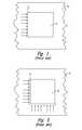
- the underfill materialtypically is dispensed into the underfill gap by injecting the underfill material along one or two sides of the flip-chip. As shown schematically in FIG. 1, a bead of an underfill material U may be dispensed along one side of the die D. The underfill material will then be drawn into the gap between the die D and the substrate S by capillary action. The direction of this movement is indicated by the arrows in FIG. 1. While such a “single stroke” process yields good results, the processing time necessary to permit the underfill material U to flow across the entire width of the die can reduce throughput of the manufacturing process.
- FIG. 2illustrates an alternative approach wherein the underfill material U is applied in an L-shaped bead which extends along two adjacent sides of the die D.
- the underfill material U dispensed along the edge(s) of the die D in this processhas a relatively high viscosity at dispensing temperatures. This permits a well-defined bead of material to be applied adjacent a single die D, facilitating a more dense arrangement of dies on the surface of the substrate.
- the substrateis typically heated sufficiently to reduce the viscosity of the underfill material. This significantly increases manufacturing time and complexity.
- U.S. Pat. No. 5,697,148(Lance Jr. et al., the teachings of which are incorporated herein by reference) also suggests dispensing an underfill material into the underfill gap through the substrate.
- the underfill materialis injected under hydraulic pressure through an injection port using a needle.
- Injecting underfill material using a dispensersuch as suggested in this patent and in the Galuschki et al. patent requires precise placement of the dispensing tip in the relatively small opening in the substrate. Fairly complex vision systems must be employed to ensure that the dispensing tip is properly aligned with the opening. Using a small dispenser also makes it more difficult to fill multiple underfill gaps between different die-substrate pairs at one time.
- the present inventionprovides certain improvements in microelectronic devices and various aspects of their manufacture.
- the inventionprovides a microelectronic device assembly which includes a microelectronic component and a first support.
- the microelectronic componenthas a facing surface, an exterior surface, and a first terminal array carried on the facing surface.
- the first supporthas a component surface, a mounting surface, a second terminal array, and an aperture which extends through the support from the component surface to the mounting surface.
- the second terminal arrayis carried on the component surface and is electrically coupled to the first terminal array of the microelectronic component.
- the aperturehas a first dimension and a second dimension less than the first dimension.
- the component surface of the supportis juxtaposed with the facing surface of the microelectronic component to define a first underfill gap between the component surface and the facing surface.
- a first underfill materialat least substantially fills the first underfill gap.
- the microelectronic device assemblyfurther includes a second support such as a circuit board.
- the first supportincludes a third terminal array on its mounting surface.
- a second supporthas a fourth terminal array carried on a terminal surface.
- the third terminal array of the first supportis electrically coupled to the fourth terminal array of the second support.
- the mounting surface of the first supportis juxtaposed with the terminal surface of the second support a define a second underfill gap therebetween.
- a second underfill materialwhich may be the same as the first underfill material, substantially fills the second underfill gap.
- Another embodiment of the inventionprovides a method for underfilling a microelectronic component which is electrically coupled to a support to define an underfill gap, with an underfill aperture extending through the support and in fluid communication with the underfill gap.
- a stencilis placed adjacent the underfill aperture, the stencil having a stencil opening in registry with the underfill aperture.
- the stencil openingdefines, at least in part, a fill volume at least as great as the volume of the underfill gap.
- the stencil openingis filled with a flowable underfill material which is permitted to flow through the support via the underfill aperture and substantially fill the first underfill gap.
- the stencilmay be removed, leaving a completed, underfilled microelectronic device assembly.
- Another embodiment of the inventionprovides a method of manufacturing a microelectronic device assembly including a support and a plurality of microelectronic components.
- Each of the microelectronic componentsmay have a facing surface carrying a terminal array and the support may have a mounting surface, a component surface carrying a plurality of terminal arrays, and a plurality of underfill apertures.
- a connecting materialis deposited on the terminal array of the microelectronic component and/or an associated one of the terminal arrays of the support.
- the facing surface of each microelectronic componentis juxtaposed with the component surface of the support such that the connecting material electrically couples the terminal array of the microelectronic component with the associated terminal array of the support.
- each microelectronic componentis spaced from the component surface of the support to define a separate underfill gap between each microelectronic component and the support. At least one of the underfill apertures in the support is in fluid communication with each of the underfill gaps.
- a stencilis placed adjacent to the mounting surface of the support, with the stencil having a separate stencil aperture in registry with each of the underfill apertures in the support.
- Each stencil aperturedefines, at least in part, a fill volume at least as great as the volume of the underfill gap in fluid communication with the underfill aperture with which the stencil aperture is registered. All of the stencil apertures are filled with a flowable underfill material, preferably in a single pass. The underfill material is permitted to flow through the support via the apertures and laterally outwardly therefrom to substantially fill each of the underfill gaps.
- the stencilmay be removed, leaving the final microelectronic device assembly.
- the inventionprovides a method of underfilling a microelectronic component which is electrically coupled to a support such that the microelectronic component and the support define an underfill gap therebetween.
- an underfill aperture in the supportis filled with an underfill material.
- the underfill aperturehas a first dimension and second dimension less than the first dimension.
- the underfill materialis allowed to flow outwardly from the underfill aperture to substantially fill the underfill gap.
- the microelectronic componenthas a pair of spaced-apart lateral edges and a pair of spaced-apart transverse edges.
- the underfill apertureis spaced farther from each of the lateral edges than from either of the transverse edges.
- the underfill materialflows outwardly from the underfill aperture a greater distance, and covers a greater surface area, in a lateral direction than in a transverse direction.
- FIG. 1is a schematic illustration of a prior art underfill process.
- FIG. 2is a schematic illustration of another prior art underfill process.
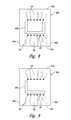
- FIG. 3is a top elevation view of a microelectronic component in accordance with an embodiment of the invention.
- FIG. 4is a top elevation view of a support which may be connected to the die of FIG. 3 in accordance with an embodiment of the invention.
- FIG. 5is top elevation view of a support in accordance with another embodiment of the invention.
- FIG. 6is a top elevation view of a support in accordance with yet another embodiment of the invention.
- FIG. 7is a top elevation view of a support in accordance with still another embodiment of the invention.
- FIG. 8is a top elevation view of a support in accordance with still another embodiment of the invention.
- FIG. 9is a top elevation view of a support in accordance with still another embodiment of the invention.
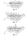
- FIGS. 10-12are side elevation views schematically illustrating a method of assembling a microelectronic device in accordance with an embodiment of the invention.
- FIG. 13is a top elevation view schematically illustrating placement of stencil to fill a plurality of underfill gaps in a single step in accordance with another alternative embodiment of the invention.
- FIG. 14is a top elevation view of a circuit board which may be coupled to the support of FIG. 4 in accordance with another embodiment of the invention.
- FIGS. 15-17are side elevation views schematically illustrating a method for assembling a microelectronic device in accordance with an alternative embodiment of the invention.
- FIGS. 3, 4, and 10 - 12schematically depict the manufacture of a microelectronic device 10 in accordance with one embodiment of the invention.
- the microelectronic device 10generally includes a microelectronic component 20 and a support 40 .
- the microelectronic component 20may be SIMM, DRAM, flash-memory, processors or any of a variety of other types of microelectronic devices.
- the microelectronic component 20will be a semiconductor device of the type commonly used in flip-chip manufacture. While the microelectronic component 20 is illustrated in the drawings as being a single element, it should be understood that the microelectronic component 20 can comprise any number of subcomponents.
- the microelectronic component 20may comprise one or more dies attached to a common substrate, such as in a stacked-die assembly.
- FIG. 3is a top view of the microelectronic component 20 .
- the microelectronic componentincludes a pair of spaced-apart lateral edges 22 a and 22 b and a pair of spaced-apart transverse edges 24 a and 24 b .
- the microelectronic component 20also includes an exterior surface 28 (FIGS. 10-12) and a facing surface 26 .
- the facing surface 26includes a terminal array 30 comprising a plurality of terminals 32 arranged on the facing surface 26 in a predefined pattern. The terminals 32 are electrically connected to functional components of the microelectronic component 20 .
- FIG. 4shows an embodiment of a support 40 which is adapted for use with the microelectronic component 20 shown in FIG. 3.
- the support 40may be flexible or rigid and have any desired configuration.
- the support 40may be formed of material commonly used to manufacture microelectronic substrates, such as ceramic, silicone, glass, or combinations thereof.
- the support 40can alternatively be formed of an organic material or other materials suitable for PCBs.
- the support 40comprises a printed circuit board such as an FR-4 PCB.
- the support 40may comprise a flexible interposer such as a conventional polyimide tape (e.g., UPILEX, commercially available from Ube Industries, Inc.
- UPILEXpolyimide tape
- the support 40 shown in FIG. 4includes a pair of spaced-apart lateral edges 42 a and 42 b and a pair of spaced-apart transverse edges 44 a and 44 b which together define the circumference of the substrate.
- the support 40is a parallelogram, with the lateral edges 42 a and 42 b being parallel to one another and perpendicular to both of the transverse edges 44 a and 44 b.
- the support 40has a component surface 46 and a mounting surface 48 (FIGS. 10-12).
- the component surface 46includes a plurality of terminals 52 defining a terminal array 50 .
- the terminals 52 on the component surface 46are arranged in a predefined pattern which may generally correspond to the pattern of the terminals 32 of the terminal array 30 on the microelectronic component 20 .
- the terminals 52 of the terminal array 50may be thought of as defining a footprint of the support 40 . If so desired, the terminals 52 may be electrically connected to functional components contained within or attached to the support 40 .
- each of the terminals 52is connected to a single mounting terminal 56 carried on the mounting surface 48 .
- These mounting terminals 56may be arranged in a predefined pattern to define a mounting terminal array 54 on the mounting surface. This can be particularly useful where the support 40 is intended to be connected to a second support, as discussed below.
- the substrate 40also includes an underfill aperture 60 which passes through the substrate from the component surface 46 to the mounting surface 48 .
- the underfill aperture 60has a first dimension 62 and second dimension 64 .
- the second dimension 64is smaller than the first dimension 62 , yielding an asymmetrical shape to the underfill aperture 60 .
- the underfill aperture 60is typified as an elongate slot.
- the first dimension 62 of the aperture 60may coincide with a major axis of the slot. This major axis may extend along a midline which is parallel to one or both of the lateral edges 42 a and 42 b.
- the larger first dimension 62 of the underfill aperture 64can be adjusted for differently sized microelectronic components 20 and supports 40 . It is anticipated that in most applications the first dimension will range from 3 mm to 25 mm.
- the smaller second dimension 64 of the underfill aperture 60may vary depending on the size and shape of the support 40 and terminal array 50 on the component surface and the nature of the underfill material. In one embodiment of the invention, the second dimension 64 ranges from 0.03 mm to 0.5 mm. To enhance flow of underfill material 74 through the underfill aperture 60 , the second dimension is desirably at least 50% greater than the largest particle size of any filler present in the underfill material.
- the aspect ratio of the underfill aperture 60i.e., the first dimension divided by the shorter second dimension
- the aspect ratiois greater than five.
- the underfill aperture 60is spaced farther from each of the lateral edges 42 a and 42 b than from either of the transverse edges 44 a and 44 b .
- the aperture 60is shown as being generally centered on the support 40 .
- the transverse distance from the periphery of the aperture 60 to a first lateral edge 42 ais the same as the transverse distance from the other side of the aperture 60 to the other lateral edge 42 b .
- the lateral distance from the periphery of the aperture to a first transverse edge 44 ais the same as the lateral distance from the periphery of the aperture 60 to the other transverse edge 44 b .
- the aperture 60need not be centered, i.e., the aperture 60 may be positioned closer to one of the lateral edges 42 a and 42 b than the other and/or closer to one of the transverse edges 44 a and 44 b than the other.
- FIG. 4also shows (in phantom) a projection of the location of the microelectronic component 20 with respect to the support 40 in one adaptation of the invention.
- the underfill aperture 60is spaced farther from at least one of the component's lateral edges 22 a and 22 b than it is from one or both of the component's transverse edges 24 a and 24 b .
- the transverse distance 66 a from the periphery of the aperture 60 to the first lateral edge 22 a of the component 20is the same as the transverse distance 66 b from the other side of the aperture 60 to the other lateral edge 22 b .
- the lateral distances 65 a and 65 b from the periphery of the aperture 60 to the component's transverse edges 24 a and 24 b , respectively,are also equal to one another. However, the transverse distances 66 a and 66 b are each greater than the lateral distances 65 a and 65 b.
- FIGS. 5-9illustrate alternative underfill apertures in accordance with an embodiment of the invention.
- the support 40 a of FIG. 5has a generally I-shaped slot 60 a .
- the support 40 b of FIG. 6includes a generally T-shaped slot 60 b .
- FIG. 7illustrates a support 40 c which has a generally star-shaped underfill aperture 60 c .
- This star-shaped aperturemay be thought of as a plurality of elongate slots which intersect one another generally at the center of the support 40 c to define the star-shaped aperture 60 c .
- the support 40 d of FIG. 8has a generally U-shaped slot 60 d and the support 40 e of FIG. 9 has a generally L-shaped slot 60 e .
- Both the U-shaped slot 60 d and the L-shaped slot 60 eare illustrated as being positioned generally within the boundaries of the terminal array 50 of the support 40 . If so desired, one or more of the legs of these slots 60 d and 60 e may be positioned outside the area bound by the terminal array 50 , e.g., between the terminal array 50 and one of the lateral edges 42 . It should be understood that the embodiments of FIGS. 4-9 are merely illustrative and a wide variety of other underfill aperture shapes could also be employed.
- the present inventionincludes methods for manufacturing microelectronic devices.
- the terminal array 30 of the microelectronic component 20is electrically coupled to the terminal array 50 on the component surface 46 of the support 40 .
- This electrical couplingmay be carried out in any known fashion.
- these componentsmay be electrically coupled using standard flip chip manufacturing techniques such as those taught in connection with FIG. 3 of U.S. Pat. No. 5,697,148, (Lance, Jr. et al., the entire teachings of which are incorporated herein by reference).
- a connecting materialis deposited on at least one of the two terminal arrays 30 and 50 which are to be connected to one another.
- solder “bumps”may be deposited on one or more terminals 32 of the microelectronic component's terminal array 30 .
- the connecting materialneed not be solder, though. Instead, it may be any of a variety of other materials known in the art, such as gold, indium, tin, lead, silver, or alloys thereof that reflow to make electrical interconnects.
- the connecting materialmay also be formed of conductive polymeric or epoxy materials, which may be plated with metals.
- the facing surface 26 of the microelectronic component 20may be juxtaposed with the component surface 46 of the support 40 , with the terminal arrays 30 and 50 generally aligned with one another.
- the connecting materialelectrically couples one or more terminals of the terminal array 30 to a corresponding terminal or terminals of the terminal array 50 on the component surface 46 , as illustrated in FIG. 10.
- the connecting materialmay then be reflowed, if necessary, to electrically couple the terminals 32 and 52 .
- the resultant electrical connector 72may also serve to mechanically connect the microelectronic component 20 to the support 40 .
- FIG. 10illustrates such a partially assembled microelectronic device 10 .
- the electrical connectors 72serve to space the facing surface 26 of the microelectronic component 20 from the support's component surface 46 . This defines a peripherally open underfill gap 70 therebetween.
- the electrical connectors 72are encompassed within the underfill gap 70 .
- the underfill gap 70is in fluid communication with the underfill aperture 60 in the support 40 . Positioning the underfill aperture 60 within the footprint of the component surface's terminal array 50 assures registry of the aperture 60 with the underfill gap 70 .
- the flip chip dieis positioned above the substrate during the underfill process.
- the partially assembled microelectronic deviceis oriented to position the support 40 above the microelectronic component 20 .
- the underfill gap 70is filled by delivering an underfill material 74 (shown schematically in FIG. 10) through the underfill aperture 60 in the support 40 .
- the underfill material 74may be selected to enhance the mechanical bond between the microelectronic component 20 and the support 40 , to help distribute stress on the microelectronic component 20 and the electrical connectors 72 , and to increase structural integrity of the microelectronic device 10 .
- the underfill materialmay also help protect the microelectronic component 20 and/or the electrical connectors 72 from degradation by contaminants, such as moisture.
- the underfill material 74is typically a polymeric material, such as an epoxy or acrylic resin, and may contain various types of inert fillers. These fillers may comprise, for example, silica particles.
- the underfill materialis typically selected to have a coefficient of thermal expansion which approximates that of the microelectronic device 20 and/or the support 40 to help minimize the stress placed on the microelectronic device 10 .
- the viscosity of the underfill material 74is selected to ensure that the underfill material will flow to fill the underfill gap 70 under the selected processing conditions. In particular, the underfill material should flow easily to fill the volume of the underfill gap 70 while minimizing voids, bubbles, and non-uniform distribution of the underfill material within the underfill gap 70 .
- the underfill material 74is desirably delivered to the underfill gap 70 utilizing at least a majority of the underfill aperture 60 .
- the underfill materialbe delivered along substantially the entire first dimension 62 of the elongated slot 60 . This may be accomplished in any of a variety of ways. If a dispensing nozzle is utilized, for example, the nozzle may be moved along the length of the aperture 60 . Alternatively, the nozzle may have an elongated dispensing tip which extends along at least a portion of the first dimension 62 while having a width which is smaller than the second dimension 64 .
- FIG. 11shows one embodiment in which the underfill material 74 is delivered to the underfill gap 70 utilizing a stencil 80 .
- the stencil 80includes a contact surface 82 , an exterior surface 84 , and a stencil aperture or opening 86 .
- the stencil aperture 86passes through the entire thickness of the stencil 80 , extending from the contact surface 82 to the exterior surface 84 .
- the shape of the stencil aperture 86may, but need not, generally correspond to the shape of the underfill aperture 60 in the substrate 40 .
- the underfill aperture 60is an elongated slot
- the stencil aperture 86may also be an elongated slot.
- the stencil aperture 86 amay be I-shaped, too. If the underfill aperture 60 b is generally T-shaped, the stencil aperture 86 b may also be T-shaped. If the underfill aperture 60 c is generally star-shaped, the stencil opening may also be generally star-shaped. As suggested in FIG. 13, though, the stencil aperture 86 c may take a different shape, such as an ellipse. If the underfill aperture 60 d is generally U-shaped, the stencil aperture may be U-shaped, and if the underfill aperture 60 e is generally L-shaped, the stencil aperture may be L-shaped.
- the stencil aperture 86is at least as large as the underfill aperture 60 and may be larger than the underfill aperture 60 .
- the stencil aperture 86may have a periphery which extends outwardly beyond the periphery of the underfill aperture 60 when these two apertures are in registry with one another.
- the width 88 of the stencil aperture 86may be greater than the width or second dimension 64 of the underfill aperture 60 .
- the length of the stencil aperture 86may also be longer than the length or first dimension 62 of the underfill aperture 60 .
- the stencil aperture 86is no larger than, and may be smaller than, the underfill aperture 60 .
- the width 88 of the stencil aperture 86may be smaller than the width or second dimension 64 of the underfill aperture 60 and the stencil aperture 86 may also be shorter than the first dimension 62 of the underfill aperture 60 .
- the entire mounting surface 40 of the support adjacent the underfill aperture 60may be covered by the stencil, reducing the volume of residue which may be left on the surface of the support 40 when the underfill process is complete.
- the stencil 80may be made of any desired material. As explained below, the stencil opening 86 can be used to control the volume of underfill material being provided to the underfill aperture 60 . As a consequence, a stencil 80 in accordance with one embodiment of the invention may be flexible, but is not readily compressed or stressed under the conditions of use outlined below. Suitable stencil materials may include metals, photoimageable polyamides, dry film photo masks, liquid photoimageable photomasks, silicon, and ceramics. If so desired, the stencil 80 may be formed of a material which is not wettable by the underfill material 74 .
- the stencil 80is positioned above the support 40 .
- the contact surface 82 of the stencil 80is in direct physical contact with the mounting surface 48 of the support 40 . This can be achieved by providing a separate stencil 80 and positioning it directly on top of the support 40 .
- the stencilshould be positioned to ensure that the stencil aperture 86 is in registry with the underfill aperture 60 .
- the mounting surface 48 of the support 40 and the contact surface 82 of the stencil 80may be provided with holes or Vernier patterns (not shown) to serve as alignment guides for aligning the stencil aperture 86 with the underfill aperture 60 .
- FIG. 80While the drawings illustrate a physically separate stencil 80 , which may be reusable, it is also contemplated that the stencil 80 may be formed directly on the mounting surface 48 of the support 40 , such as by using a coating of a liquid photoimageable photomask. The stencil 80 may be held in place with respect to the support 40 by tensioning the stencil 80 using a frame (not shown) that holds the edges of the stencil against the support 40 .
- the underfill materials 74may be delivered to the underfill aperture 60 via the stencil aperture 86 . This may be accomplished, for example, by “squeegeeing.” In accordance with this embodiment, a quantity of the underfill material 74 is applied to the exterior surface 84 of the stencil 80 . A squeegee blade 90 may then be dragged across the exterior surface 84 , passing over the stencil aperture 86 . This will deliver a predictable volume of the underfill material 74 to the stencil aperture 86 .
- the volume of underfill material 74 delivered through the stencil aperturewill depend, in part, on the thickness of the stencil 80 and the surface area of the stencil aperture 86 .
- the stencil aperture 86is in registry with the underfill aperture 60 .
- at least a portion of the underfill material 74may pass into the underfill aperture 60 during the process of squeegeeing.
- the amount of underfill materials 74 which passes into the underfill aperture 60 as the blade 90 passes over the stencil aperture 86will depend, in part, on the viscosity of the underfill material 74 .
- the stencil aperture 86may only partly define the fill volume of underfill material being delivered in the squeegeeing process.
- the fill volume so definedshould be at least as great as the volume of the underfill gap 70 to ensure that the underfill gap 70 is substantially filled with underfill material 74 .
- the underfill material 74is permitted to flow through the stencil aperture 86 and the underfill aperture 60 into the underfill gap 70 .
- the fill characteristics of the underfill material 74may be selected to permit the fill material to substantially fill the underfill gap 70 , readily flowing around the electrical connectors 72 to encapsulate and protect the connectors 72 , as shown in FIG. 12.
- the viscosity of the underfill materialmay be selected so it may fill the underfill gap without aid of hydraulic pressure, relying instead on gravity and/or capillary action, for example.
- the viscosity of the underfill material at the temperature under which the squeegeeing takes placelimits the flow of underfill material into the underfill gap 70 .
- the viscosity of the underfill materialmay then be reduced, e.g., by heating, permitting the underfill material to flow through the underfill aperture 60 and substantially fill the underfill gap without requiring hydraulic pressure.
- the viscosity of the underfill materialis relatively low even at room temperature.
- the underfill materialcan flow through the underfill aperture 60 and substantially fill the underfill gap 70 at room temperature without the aid of hydraulic pressure. While the control of the volume of underfill material 74 delivered to the aperture 86 may be a little less precise, a predictable volume can be delivered by consistently controlling the speed and contact pressure of the squeegee blade 90 during the squeegeeing process.
- the underfill aperture 60is spaced farther from at least one of the microelectronic component's lateral edges 22 a and 22 b than from at least one of the microelectronic component's transverse edges 24 a and 24 b .
- the transverse distances 66 a and 66 b from the underfill aperture 60 to lateral edges 22 a and 22 b , respectivelyare both greater than either of the lateral distances 65 a and 65 b between the underfill aperture 60 and the transverse edges 24 a and 24 b , respectively.
- the underfill materialflows outwardly away from the underfill aperture 60 to fill the underfill gap 70 , it will travel a greater distance laterally than it will travel transversely to reach the outer edge of the microelectronic component 20 .
- the surface area of the microelectronic component 20 being covered by the underfill materialwill also be proportional to the distance traveled, dictating that the underfill material will cover a greater surface area laterally than it does transversely as it flows outwardly away from the underfill aperture 60 .
- the position of the underfill aperture 60 with respect to the support 40can appreciably reduce processing time and cost in manufacturing microelectronic devices 10 in accordance with the invention.
- Applying the bead of underfill material U along a single edge of the die Drequires that the underfill material U flow across the entire width of the die D. Applying the underfill material U along to adjacent edges of the die D, as shown in FIG. 2, can reduce the average distance which the underfill material U must travel to completely fill the underfill gap. However, as the two fronts of the underfill material converge, they may trap air, creating voids in the underfill material. Additionally, at least some of the underfill material must travel the entire width of the die D to reach the farthest corner of the die.
- Delivering the underfill material through the underfill aperture 60reduces the distance which the underfill material has to travel to fill the underfill gap 70 . For a given underfill material, this will decrease the processing time necessary to fill the underfill gap 70 . Notably, surface tension will also tend to keep the underfill material 74 from flowing beyond the outer edge of the support 40 . As a consequence, delivering the underfill material 74 to the underfill gap 70 via the underfill aperture 60 allows multiple microelectronic components 20 to be added to a single support without risk that capillary action will draw underfill material U intended for one die D under an adjacent component on the associated substrate S, which is a risk in the process shown in FIGS. 1 and 2.
- U.S. Pat. No. 5,697,148proposes pumping an underfill material through a small hole drilled through a substrate. As can be seen in FIG. 5 of this patent, this still requires that the underfill material flow a substantial distance to completely fill the underfill gap.
- Using an elongate underfill aperture 60 in accordance with an embodiment of the present inventioncan materially reduce the distance which the underflow material must travel to fill the underfill gap 70 .
- the relatively restrictive opening through the substrate suggested in this and other patentslimits the rate at which the underfill material can be delivered to the underfill gap.
- the underfill aperture 60 in accordance with one embodiment of the present inventionprovides a materially greater surface area through which the underfill material can be delivered without unduly sacrificing useful substrate real estate which can be used to position functional elements or interconnects in the substrate beneath the microelectronic component 20 .
- the underfill aperture 60provides a wider passage way through which underfill material can pass, reducing the pressure needed to get the underfill material into the underfill gap in a reasonable period of time. This also facilitates delivery of the underfill material using the stencil 80 as discussed above.
- the stencil 80may be removed. In one embodiment, the stencil remains in place until the underfill material has flowed to fill the underfill gap. Thereafter, the stencil 80 may be removed, such as by lifting it off the mounting surface 48 of the support 40 . Alternatively, the stencil may be removed by chemical etching or use of a solvent which would remove the stencil 80 from the support 40 . Particularly, if a higher viscosity underfill material 74 is used and subsequently heated to fill the underfill gap 70 , the stencil can be removed before the underfill material fills the underfill gap 70 .
- FIGS. 4-12illustrate embodiments of the invention which utilize a single underfill aperture to fill a single underfill gap beneath a single microelectronic device.
- Using a stencil in accordance with an embodiment to the present inventioncan allow the underfilling of multiple underfill gaps in a single step.
- a single substrate 40is provided with multiple microelectronic components 20 , as shown in FIG. 13.
- the process of attaching each microelectronic component 20 the substratemay be generally as outlined above.
- the support 40may be provided with multiple terminal arrays, with each terminal array being associated with one of the microelectronic components 20 to be added to the support 40 .
- a connecting materialcan be deposited on one or both of the microelectronic component's terminal array and the associated terminal array of the support.
- the facing surface of each microelectronic componentmay then be juxtaposed with the component surface of the support such that the connecting material electrically couples the terminal array of the components with the associated terminal arrays of the support.
- the stencilmay be applied to the mounting surface 48 of the support with a separate stencil aperture 86 , 86 a , 86 b or 86 c in registry with one of the underfill apertures 60 , 60 a , 60 b or 60 c in the support 40 .
- a single, relatively large quantity of underfill material 74may be applied to the exterior surface 84 of the stencil 80 .
- a squeegee blade(not shown in FIG. 13) may then be moved across the exterior surface 84 of the stencil 80 , thereby filling all of the stencil apertures with underfill material in a single pass.
- FIG. 13illustrates a single microelectronic device 10 having a wide variety of differently sized microelectronic components 20 and a wide variety of shapes and sizes of underfill apertures 60 , 60 a , 60 b , and 60 c . This is done primarily to illustrate how various stencil aperture configurations can be positioned in relation to different underfill apertures. It should be understood that in many circumstances all of the underfill apertures and stencil apertures will be of substantially the same size and orientation.
- This methodallows a single substrate 40 with multiple microelectronic components 20 and multiple underfill gaps to be filled in a single pass.
- the support 40is subsequently divided into a plurality of separate supports, each of which carries at least one of the microelectronic components.
- the supportmay be divided either before or after removing the stencil 80 . This facilitates the mass manufacture of smaller microelectronic devices by filling in the underfill gaps of multiple microelectronic devices in one simple step.
- a plurality of partially assembled microelectronic devicesare positioned adjacent to one another.
- the partially assembled microelectronic devicesmay comprise one or more microelectronic components 20 attached to a single substrate 40 , such as illustrated in FIG. 10.
- These microelectronic device assembliesneed not be positioned immediately adjacent to or abutting one another; they need only be positioned close enough to enable them to be covered using a single stencil.
- the supports 40are desirably aligned such that their mounting surfaces 40 are generally co-planar.
- the stencil 80may have a plurality of stencil apertures 86 and the stencil would be positioned such that at least one of the stencil apertures 86 is in registry with at least one underfill aperture 60 of each of the supports 40 . All of the stencil apertures 86 may be filled with flowable underfill material in a single pass, as discussed above in connection with FIG. 13. The underfill material may be permitted to flow through each of the supports via their respective underfill apertures to fill each of the underfill gaps. Removing the stencil 80 will yield a plurality of co-formed microelectronic device assemblies 10 .
- FIG. 14schematically illustrates a stylized circuit board 110 which may be used in connection with a further embodiment of the invention.
- This circuit board 110has a pair of spaced-apart lateral edges 112 a and 112 b and a pair of spaced-apart transverse edges 114 a and 114 b .
- the circuit board 110includes a terminal surface 116 and an outer surface 118 (FIG. 15).
- the terminal surface 116bears a plurality of terminals 122 which define a terminal array 120 .
- This terminal array 120is configured to be electrically coupled to the terminal array 54 on the mounting surface 48 of the support 40 (shown in FIG. 4).
- the circuit board 110is shown as including a plurality of additional components 125 and an interface 126 which can be used to connect the circuit board to another device. If so desired, the circuit board 110 may be a rigid PCB, though any of the materials noted above in connection with the support 40 could be used instead.
- the circuit board 110also includes a second underfill aperture 130 which extends through the thickness of the circuit board 110 from its terminal surface 116 to its outer surface 118 .
- the second underfill aperturehas a first dimension 132 and a second dimension 134 which is less than the first dimension 132 .
- the second underfill aperture 130 in FIG. 14is typified as an elongated slot. It should be understood, though, that this second underfill aperture 130 may take on a variety of different shapes, e.g., shapes analogous to the underfill apertures shown in FIGS. 5-9.
- FIGS. 15-17schematically illustrate a method of one embodiment to the invention for assembling a microelectronic device 10 such as that discussed above with a circuit board 110 or other second support. This yields a larger microelectronic device 100 in which the microelectronic device 10 discussed above may be considered a subassembly.
- the process illustrated in FIGS. 15-17is directly analogous to the process outlined above in connection with FIGS. 10-12.
- the terminal array 120 of the circuit board 110will be electrically coupled to the terminal array 54 on the support's mounting surface 48 via electrical connectors 142 . This will define a second underfill gap 140 between the circuit board 110 and the support 140 .
- the second underfill aperture 130is shown as being about the same size and positioned vertically directly above the first underfill aperture 60 . It should be understood, however, that this is not necessary and the two underfill apertures 60 , 130 can be different sizes and positioned in different locations or orientations with respect to one another.
- the second underfill gap 140may be filled with a second underfill material 144 in any desired fashion.
- a second underfill material 144may be filled using a stencil 80 and squeegee blade 90 generally outlined above in connection with FIGS. 10-12.
- the second underfill materialnot only fills the gap between the second support's terminal surface 116 and the other support's mounting surface 148 , but also fills any remaining void in the underfill aperture 60 in the support 40 . This can be facilitated by positioning the second underfill aperture 130 directly above the first underfill aperture 60 .
- the second underfill material 144may be different from the underfill material 74 . This may be advantageous if different design objectives are required of the second underfill material 144 . In one embodiment of the invention, however, both of the underfill materials 74 and 144 have the same composition.
- FIGS. 15-17The process outlined in FIGS. 15-17 start with a microelectronic device 10 wherein the underfill gap 70 is already filled with underfill material 74 before the microelectronic device 10 is attached to the second support 110 . Thereafter, the second underfill gap 140 is filled with the second underfill material 144 is a separate step.
- the first underfill gap 70 and the second underfill gap 140are filled with a common underfill material in a single step.
- the underfill aperture 60 in the first support 40is in fluid communication with the second underfill gap 140 .
- the second underfill aperture 130may be positioned directly above the first underfill aperture 60 .
- the first and second underfill gaps 70 and 140may then be filled with a common underfill material 74 in a single step, e.g., using a stencil 80 and squeegee blade 90 analogous to that discussed above in the context of FIGS. 10-12.
Landscapes
- Engineering & Computer Science (AREA)
- Computer Hardware Design (AREA)
- Microelectronics & Electronic Packaging (AREA)
- Power Engineering (AREA)
- Physics & Mathematics (AREA)
- Condensed Matter Physics & Semiconductors (AREA)
- General Physics & Mathematics (AREA)
- Manufacturing & Machinery (AREA)
- Encapsulation Of And Coatings For Semiconductor Or Solid State Devices (AREA)
- Wire Bonding (AREA)
Abstract
Description
- This application is a divisional application of U.S. patent application Ser. No. 09/944,465, entitled “METHOD OF MANUFACTURING MICROELECTRONIC DEVICES, INCLUDING METHODS OF UNDERFILLING MICROELECTRONIC COMPONENTS THROUGH AN UNDERFILL APERTURE,” filed Aug. 30, 2001, now U.S. Pat. No. 6,756,251, issued Jun. 29, 2004, which claims foreign priority benefits of Singapore Application No. 200105099-6, filed Aug. 21, 2001, both of which are herein incorporated by reference in their entireties.[0001]
- This invention relates to microelectronic devices having microelectronic components mounted on substrates and methods of manufacturing such devices. The invention has particular utility in connection with flip-chip packaging.[0002]
- Microelectronic devices, such as memory devices and microprocessors, typically include one or more microelectronic components attached to a substrate. The microelectronic components commonly include at least one die including functional features such as memory cells, processor circuits, and interconnecting circuitry. The dies of the microelectronic components may be encased in a plastic, ceramic or metal protective covering. Each die commonly includes an array of very small bond pads electrically coupled to the functional features. These terminals can be used to operatively connect the microelectronic component to the substrate.[0003]
- One type of microelectronic component which is gaining increased acceptance is the “flip-chip” semiconductor device. These components are referred to as “flip-chips” because they are typically manufactured in wafer form having bond pads which are initially facing upwardly. After manufacture is completed and the semiconductor die is singulated from the wafer, it is inverted or “flipped” such that the surface bearing the bond pads faces downwardly for attachment to a substrate. The bond pads are usually coupled to terminals, such as conductive “bumps,” which are used as electrical and mechanical connectors connecting the die to the substrate. A variety of materials may be used to form the bumps on the flip-chip, such as various types of solder and conductive polymers. In applications using solder bumps, the solder bumps are reflowed to form a solder joint between the flip-chip component and the substrate. This leaves a small gap between the flip-chip and the substrate. To enhance the joint integrity between the microelectronic component and the substrate, an underfill material is introduced into the gap between the components. This underfill material helps equalize stress placed on the components and protects the components from contaminants, such as moisture and chemicals.[0004]
- The underfill material typically is dispensed into the underfill gap by injecting the underfill material along one or two sides of the flip-chip. As shown schematically in FIG. 1, a bead of an underfill material U may be dispensed along one side of the die D. The underfill material will then be drawn into the gap between the die D and the substrate S by capillary action. The direction of this movement is indicated by the arrows in FIG. 1. While such a “single stroke” process yields good results, the processing time necessary to permit the underfill material U to flow across the entire width of the die can reduce throughput of the manufacturing process.[0005]
- FIG. 2 illustrates an alternative approach wherein the underfill material U is applied in an L-shaped bead which extends along two adjacent sides of the die D. By reducing the average distance which the underfill material has to flow to fill the underfill gap, processing times can be reduced. However, this L-stroke approach can lead to more voids in the underfill material, adversely affecting the integrity of the bond between the die D and the substrate S.[0006]
- Typically, the underfill material U dispensed along the edge(s) of the die D in this process has a relatively high viscosity at dispensing temperatures. This permits a well-defined bead of material to be applied adjacent a single die D, facilitating a more dense arrangement of dies on the surface of the substrate. To get the underfill material U to flow into the underflow gap, the substrate is typically heated sufficiently to reduce the viscosity of the underfill material. This significantly increases manufacturing time and complexity.[0007]
- Others have proposed pumping an underfill material into the underfill gap through an opening in the substrate. For example, U.S. Pat. No. 6,057,178 (Galuschki et al, the teachings of which are incorporated herein by reference) adds the underfill material via an orifice in the substrate. A viscous underfill material is added to the orifice ( e.g., by dispensing it under pressure). The assembly must then be heated to allow the underfill material to flow into the underfill gap.[0008]
- U.S. Pat. No. 5,697,148 (Lance Jr. et al., the teachings of which are incorporated herein by reference) also suggests dispensing an underfill material into the underfill gap through the substrate. The underfill material is injected under hydraulic pressure through an injection port using a needle. Injecting underfill material using a dispenser such as suggested in this patent and in the Galuschki et al. patent requires precise placement of the dispensing tip in the relatively small opening in the substrate. Fairly complex vision systems must be employed to ensure that the dispensing tip is properly aligned with the opening. Using a small dispenser also makes it more difficult to fill multiple underfill gaps between different die-substrate pairs at one time.[0009]
- The present invention provides certain improvements in microelectronic devices and various aspects of their manufacture. In accordance with one embodiment, the invention provides a microelectronic device assembly which includes a microelectronic component and a first support. The microelectronic component has a facing surface, an exterior surface, and a first terminal array carried on the facing surface. The first support has a component surface, a mounting surface, a second terminal array, and an aperture which extends through the support from the component surface to the mounting surface. The second terminal array is carried on the component surface and is electrically coupled to the first terminal array of the microelectronic component. The aperture has a first dimension and a second dimension less than the first dimension. The component surface of the support is juxtaposed with the facing surface of the microelectronic component to define a first underfill gap between the component surface and the facing surface. A first underfill material at least substantially fills the first underfill gap.[0010]
- In an alternative embodiment, the microelectronic device assembly further includes a second support such as a circuit board. In this embodiment, the first support includes a third terminal array on its mounting surface. A second support has a fourth terminal array carried on a terminal surface. The third terminal array of the first support is electrically coupled to the fourth terminal array of the second support. The mounting surface of the first support is juxtaposed with the terminal surface of the second support a define a second underfill gap therebetween. A second underfill material, which may be the same as the first underfill material, substantially fills the second underfill gap.[0011]
- Another embodiment of the invention provides a method for underfilling a microelectronic component which is electrically coupled to a support to define an underfill gap, with an underfill aperture extending through the support and in fluid communication with the underfill gap. In accordance with this method, a stencil is placed adjacent the underfill aperture, the stencil having a stencil opening in registry with the underfill aperture. The stencil opening defines, at least in part, a fill volume at least as great as the volume of the underfill gap. The stencil opening is filled with a flowable underfill material which is permitted to flow through the support via the underfill aperture and substantially fill the first underfill gap. The stencil may be removed, leaving a completed, underfilled microelectronic device assembly.[0012]
- Another embodiment of the invention provides a method of manufacturing a microelectronic device assembly including a support and a plurality of microelectronic components. Each of the microelectronic components may have a facing surface carrying a terminal array and the support may have a mounting surface, a component surface carrying a plurality of terminal arrays, and a plurality of underfill apertures. For each microelectronic component, a connecting material is deposited on the terminal array of the microelectronic component and/or an associated one of the terminal arrays of the support. The facing surface of each microelectronic component is juxtaposed with the component surface of the support such that the connecting material electrically couples the terminal array of the microelectronic component with the associated terminal array of the support. The facing surface of each microelectronic component is spaced from the component surface of the support to define a separate underfill gap between each microelectronic component and the support. At least one of the underfill apertures in the support is in fluid communication with each of the underfill gaps. A stencil is placed adjacent to the mounting surface of the support, with the stencil having a separate stencil aperture in registry with each of the underfill apertures in the support. Each stencil aperture defines, at least in part, a fill volume at least as great as the volume of the underfill gap in fluid communication with the underfill aperture with which the stencil aperture is registered. All of the stencil apertures are filled with a flowable underfill material, preferably in a single pass. The underfill material is permitted to flow through the support via the apertures and laterally outwardly therefrom to substantially fill each of the underfill gaps. The stencil may be removed, leaving the final microelectronic device assembly.[0013]
- In accordance with still another embodiment, the invention provides a method of underfilling a microelectronic component which is electrically coupled to a support such that the microelectronic component and the support define an underfill gap therebetween. According to this method, an underfill aperture in the support is filled with an underfill material. The underfill aperture has a first dimension and second dimension less than the first dimension. The underfill material is allowed to flow outwardly from the underfill aperture to substantially fill the underfill gap. In one particular adaptation of this embodiment, the microelectronic component has a pair of spaced-apart lateral edges and a pair of spaced-apart transverse edges. The underfill aperture is spaced farther from each of the lateral edges than from either of the transverse edges. The underfill material flows outwardly from the underfill aperture a greater distance, and covers a greater surface area, in a lateral direction than in a transverse direction.[0014]
- FIG. 1 is a schematic illustration of a prior art underfill process.[0015]
- FIG. 2 is a schematic illustration of another prior art underfill process.[0016]
- FIG. 3 is a top elevation view of a microelectronic component in accordance with an embodiment of the invention.[0017]
- FIG. 4 is a top elevation view of a support which may be connected to the die of FIG. 3 in accordance with an embodiment of the invention.[0018]
- FIG. 5 is top elevation view of a support in accordance with another embodiment of the invention.[0019]
- FIG. 6 is a top elevation view of a support in accordance with yet another embodiment of the invention.[0020]
- FIG. 7 is a top elevation view of a support in accordance with still another embodiment of the invention.[0021]
- FIG. 8 is a top elevation view of a support in accordance with still another embodiment of the invention.[0022]
- FIG. 9 is a top elevation view of a support in accordance with still another embodiment of the invention.[0023]
- FIGS. 10-12 are side elevation views schematically illustrating a method of assembling a microelectronic device in accordance with an embodiment of the invention.[0024]
- FIG. 13 is a top elevation view schematically illustrating placement of stencil to fill a plurality of underfill gaps in a single step in accordance with another alternative embodiment of the invention.[0025]
- FIG. 14 is a top elevation view of a circuit board which may be coupled to the support of FIG. 4 in accordance with another embodiment of the invention.[0026]
- FIGS. 15-17 are side elevation views schematically illustrating a method for assembling a microelectronic device in accordance with an alternative embodiment of the invention.[0027]
- Various embodiments of the present invention provide microelectronic devices or methods of manufacturing microelectronic devices. The following description provides specific details of certain embodiments of the invention illustrated in the drawings to provide a thorough understanding of those embodiments. It should be recognized, however, that the present invention can be reflected in additional embodiments and the invention may be practiced without some of the details in the following description.[0028]
- FIGS. 3, 4, and[0029]10-12 schematically depict the manufacture of a
microelectronic device 10 in accordance with one embodiment of the invention. Themicroelectronic device 10 generally includes amicroelectronic component 20 and asupport 40. Themicroelectronic component 20 may be SIMM, DRAM, flash-memory, processors or any of a variety of other types of microelectronic devices. Typically, themicroelectronic component 20 will be a semiconductor device of the type commonly used in flip-chip manufacture. While themicroelectronic component 20 is illustrated in the drawings as being a single element, it should be understood that themicroelectronic component 20 can comprise any number of subcomponents. For example, themicroelectronic component 20 may comprise one or more dies attached to a common substrate, such as in a stacked-die assembly. - FIG. 3 is a top view of the[0030]
microelectronic component 20. The microelectronic component includes a pair of spaced-apart lateral edges22aand22band a pair of spaced-aparttransverse edges microelectronic component 20 also includes an exterior surface28 (FIGS. 10-12) and a facingsurface 26. The facingsurface 26 includes aterminal array 30 comprising a plurality ofterminals 32 arranged on the facingsurface 26 in a predefined pattern. Theterminals 32 are electrically connected to functional components of themicroelectronic component 20. - FIG. 4 shows an embodiment of a[0031]
support 40 which is adapted for use with themicroelectronic component 20 shown in FIG. 3. Thesupport 40 may be flexible or rigid and have any desired configuration. Thesupport 40 may be formed of material commonly used to manufacture microelectronic substrates, such as ceramic, silicone, glass, or combinations thereof. Thesupport 40 can alternatively be formed of an organic material or other materials suitable for PCBs. In one embodiment of the invention, thesupport 40 comprises a printed circuit board such as an FR-4 PCB. In another embodiment, thesupport 40 may comprise a flexible interposer such as a conventional polyimide tape ( e.g., UPILEX, commercially available from Ube Industries, Inc. of Tokyo, Japan; KAPTON or MICROLUX, both commercially available from E. I. du Pont de Nemours and Co. of Delaware, USA; or ESPANEX, commercially available from Nippon Steel Chemical Co., Ltd. of Tokyo, Japan) and thismicroelectronic device 10 may be attached to a circuit board, as mentioned below in connection with FIGS. 15-17. - The[0032]
support 40 shown in FIG. 4 includes a pair of spaced-apart lateral edges42aand42band a pair of spaced-aparttransverse edges support 40 is a parallelogram, with the lateral edges42aand42bbeing parallel to one another and perpendicular to both of thetransverse edges - The[0033]
support 40 has acomponent surface 46 and a mounting surface48 (FIGS. 10-12). Thecomponent surface 46 includes a plurality ofterminals 52 defining aterminal array 50. Theterminals 52 on thecomponent surface 46 are arranged in a predefined pattern which may generally correspond to the pattern of theterminals 32 of theterminal array 30 on themicroelectronic component 20. Theterminals 52 of theterminal array 50 may be thought of as defining a footprint of thesupport 40. If so desired, theterminals 52 may be electrically connected to functional components contained within or attached to thesupport 40. In the illustrated embodiment, each of theterminals 52 is connected to a single mountingterminal 56 carried on the mountingsurface 48. These mountingterminals 56 may be arranged in a predefined pattern to define a mountingterminal array 54 on the mounting surface. This can be particularly useful where thesupport 40 is intended to be connected to a second support, as discussed below. - The[0034]
substrate 40 also includes anunderfill aperture 60 which passes through the substrate from thecomponent surface 46 to the mountingsurface 48. Theunderfill aperture 60 has afirst dimension 62 andsecond dimension 64. Thesecond dimension 64 is smaller than thefirst dimension 62, yielding an asymmetrical shape to theunderfill aperture 60. In FIG. 4, theunderfill aperture 60 is typified as an elongate slot. Thefirst dimension 62 of theaperture 60 may coincide with a major axis of the slot. This major axis may extend along a midline which is parallel to one or both of the lateral edges42aand42b. - The larger[0035]
first dimension 62 of theunderfill aperture 64 can be adjusted for differently sizedmicroelectronic components 20 and supports40. It is anticipated that in most applications the first dimension will range from 3 mm to 25 mm. The smallersecond dimension 64 of theunderfill aperture 60 may vary depending on the size and shape of thesupport 40 andterminal array 50 on the component surface and the nature of the underfill material. In one embodiment of the invention, thesecond dimension 64 ranges from 0.03 mm to 0.5 mm. To enhance flow ofunderfill material 74 through theunderfill aperture 60, the second dimension is desirably at least 50% greater than the largest particle size of any filler present in the underfill material. The aspect ratio of the underfill aperture60 (i.e., the first dimension divided by the shorter second dimension) is greater than one. In one embodiment of the invention, the aspect ratio is greater than five. - In the embodiment of FIG. 4, the[0036]
underfill aperture 60 is spaced farther from each of the lateral edges42aand42bthan from either of thetransverse edges aperture 60 is shown as being generally centered on thesupport 40. In particular, the transverse distance from the periphery of theaperture 60 to a firstlateral edge 42ais the same as the transverse distance from the other side of theaperture 60 to the otherlateral edge 42b. Similarly, the lateral distance from the periphery of the aperture to a firsttransverse edge 44ais the same as the lateral distance from the periphery of theaperture 60 to the othertransverse edge 44b. It should be understood, though, that theaperture 60 need not be centered, i.e., theaperture 60 may be positioned closer to one of the lateral edges42aand42bthan the other and/or closer to one of thetransverse edges - FIG. 4 also shows (in phantom) a projection of the location of the[0037]
microelectronic component 20 with respect to thesupport 40 in one adaptation of the invention. When the support is so positioned, theunderfill aperture 60 is spaced farther from at least one of the component's lateral edges22aand22bthan it is from one or both of the component'stransverse edges transverse distance 66afrom the periphery of theaperture 60 to the firstlateral edge 22aof thecomponent 20 is the same as thetransverse distance 66bfrom the other side of theaperture 60 to the otherlateral edge 22b. The lateral distances65aand65bfrom the periphery of theaperture 60 to the component'stransverse edges transverse distances - FIGS. 5-9 illustrate alternative underfill apertures in accordance with an embodiment of the invention. The[0038]
support 40aof FIG. 5 has a generally I-shapedslot 60a. Thesupport 40bof FIG. 6 includes a generally T-shapedslot 60b. FIG. 7 illustrates asupport 40cwhich has a generally star-shapedunderfill aperture 60c. This star-shaped aperture may be thought of as a plurality of elongate slots which intersect one another generally at the center of thesupport 40cto define the star-shapedaperture 60c. Thesupport 40dof FIG. 8 has a generallyU-shaped slot 60dand thesupport 40eof FIG. 9 has a generally L-shapedslot 60e. Both theU-shaped slot 60dand the L-shapedslot 60eare illustrated as being positioned generally within the boundaries of theterminal array 50 of thesupport 40. If so desired, one or more of the legs of theseslots terminal array 50, e.g., between theterminal array 50 and one of the lateral edges42. It should be understood that the embodiments of FIGS. 4-9 are merely illustrative and a wide variety of other underfill aperture shapes could also be employed. - As noted above, the present invention includes methods for manufacturing microelectronic devices. In the following discussion, reference will be made to the[0039]
microelectronic component 20 and thesupport 40 shown in FIGS. 3 and 4. It should be understood, though, that many of the features shown in these drawings are not required for manufacturing a microelectronic device according to the methods outlined below. - Initially, the[0040]
terminal array 30 of themicroelectronic component 20 is electrically coupled to theterminal array 50 on thecomponent surface 46 of thesupport 40. This electrical coupling may be carried out in any known fashion. For example, these components may be electrically coupled using standard flip chip manufacturing techniques such as those taught in connection with FIG. 3 of U.S. Pat. No. 5,697,148, (Lance, Jr. et al., the entire teachings of which are incorporated herein by reference). - Techniques for electrically coupling microelectronic components to supports are well known in the art and need not be discussed in great detail here. Briefly, though, a connecting material is deposited on at least one of the two[0041]
terminal arrays more terminals 32 of the microelectronic component'sterminal array 30. The connecting material need not be solder, though. Instead, it may be any of a variety of other materials known in the art, such as gold, indium, tin, lead, silver, or alloys thereof that reflow to make electrical interconnects. The connecting material may also be formed of conductive polymeric or epoxy materials, which may be plated with metals. - The facing[0042]
surface 26 of themicroelectronic component 20 may be juxtaposed with thecomponent surface 46 of thesupport 40, with theterminal arrays terminal array 30 to a corresponding terminal or terminals of theterminal array 50 on thecomponent surface 46, as illustrated in FIG. 10. The connecting material may then be reflowed, if necessary, to electrically couple theterminals electrical connector 72 may also serve to mechanically connect themicroelectronic component 20 to thesupport 40. - FIG. 10 illustrates such a partially assembled[0043]
microelectronic device 10. As can be seen in this drawing, theelectrical connectors 72 serve to space the facingsurface 26 of themicroelectronic component 20 from the support'scomponent surface 46. This defines a peripherallyopen underfill gap 70 therebetween. Theelectrical connectors 72 are encompassed within theunderfill gap 70. Theunderfill gap 70 is in fluid communication with theunderfill aperture 60 in thesupport 40. Positioning theunderfill aperture 60 within the footprint of the component surface'sterminal array 50 assures registry of theaperture 60 with theunderfill gap 70. - In conventional manufacture, the flip chip die is positioned above the substrate during the underfill process. In accordance with one embodiment of the present invention, though, the partially assembled microelectronic device is oriented to position the[0044]
support 40 above themicroelectronic component 20. - The[0045]
underfill gap 70 is filled by delivering an underfill material74 (shown schematically in FIG. 10) through theunderfill aperture 60 in thesupport 40. Theunderfill material 74 may be selected to enhance the mechanical bond between themicroelectronic component 20 and thesupport 40, to help distribute stress on themicroelectronic component 20 and theelectrical connectors 72, and to increase structural integrity of themicroelectronic device 10. The underfill material may also help protect themicroelectronic component 20 and/or theelectrical connectors 72 from degradation by contaminants, such as moisture. - The[0046]
underfill material 74 is typically a polymeric material, such as an epoxy or acrylic resin, and may contain various types of inert fillers. These fillers may comprise, for example, silica particles. The underfill material is typically selected to have a coefficient of thermal expansion which approximates that of themicroelectronic device 20 and/or thesupport 40 to help minimize the stress placed on themicroelectronic device 10. As discussed in more detail below, the viscosity of theunderfill material 74 is selected to ensure that the underfill material will flow to fill theunderfill gap 70 under the selected processing conditions. In particular, the underfill material should flow easily to fill the volume of theunderfill gap 70 while minimizing voids, bubbles, and non-uniform distribution of the underfill material within theunderfill gap 70. - The[0047]
underfill material 74 is desirably delivered to theunderfill gap 70 utilizing at least a majority of theunderfill aperture 60. Looking at thesupport 40 of FIG. 4, for example, it is desirable that the underfill material be delivered along substantially the entirefirst dimension 62 of theelongated slot 60. This may be accomplished in any of a variety of ways. If a dispensing nozzle is utilized, for example, the nozzle may be moved along the length of theaperture 60. Alternatively, the nozzle may have an elongated dispensing tip which extends along at least a portion of thefirst dimension 62 while having a width which is smaller than thesecond dimension 64. - FIG. 11 shows one embodiment in which the[0048]
underfill material 74 is delivered to theunderfill gap 70 utilizing astencil 80. Thestencil 80 includes acontact surface 82, anexterior surface 84, and a stencil aperture oropening 86. Thestencil aperture 86 passes through the entire thickness of thestencil 80, extending from thecontact surface 82 to theexterior surface 84. As suggested in FIG. 13 (discussed in more detail below), the shape of thestencil aperture 86 may, but need not, generally correspond to the shape of theunderfill aperture 60 in thesubstrate 40. For example, if theunderfill aperture 60 is an elongated slot, thestencil aperture 86 may also be an elongated slot. If theunderfill aperture 60ais generally I-shaped, thestencil aperture 86amay be I-shaped, too. If theunderfill aperture 60bis generally T-shaped, thestencil aperture 86bmay also be T-shaped. If theunderfill aperture 60cis generally star-shaped, the stencil opening may also be generally star-shaped. As suggested in FIG. 13, though, thestencil aperture 86cmay take a different shape, such as an ellipse. If theunderfill aperture 60dis generally U-shaped, the stencil aperture may be U-shaped, and if theunderfill aperture 60eis generally L-shaped, the stencil aperture may be L-shaped. - In one embodiment, the[0049]
stencil aperture 86 is at least as large as theunderfill aperture 60 and may be larger than theunderfill aperture 60. In particular, thestencil aperture 86 may have a periphery which extends outwardly beyond the periphery of theunderfill aperture 60 when these two apertures are in registry with one another. For example, thewidth 88 of thestencil aperture 86 may be greater than the width orsecond dimension 64 of theunderfill aperture 60. The length of thestencil aperture 86 may also be longer than the length orfirst dimension 62 of theunderfill aperture 60. - In an alternative embodiment (not specifically illustrated), the[0050]
stencil aperture 86 is no larger than, and may be smaller than, theunderfill aperture 60. For example, thewidth 88 of thestencil aperture 86 may be smaller than the width orsecond dimension 64 of theunderfill aperture 60 and thestencil aperture 86 may also be shorter than thefirst dimension 62 of theunderfill aperture 60. In such an embodiment, the entire mountingsurface 40 of the support adjacent theunderfill aperture 60 may be covered by the stencil, reducing the volume of residue which may be left on the surface of thesupport 40 when the underfill process is complete. - The[0051]
stencil 80 may be made of any desired material. As explained below, thestencil opening 86 can be used to control the volume of underfill material being provided to theunderfill aperture 60. As a consequence, astencil 80 in accordance with one embodiment of the invention may be flexible, but is not readily compressed or stressed under the conditions of use outlined below. Suitable stencil materials may include metals, photoimageable polyamides, dry film photo masks, liquid photoimageable photomasks, silicon, and ceramics. If so desired, thestencil 80 may be formed of a material which is not wettable by theunderfill material 74. - In use, the[0052]
stencil 80 is positioned above thesupport 40. In the illustrated embodiment, thecontact surface 82 of thestencil 80 is in direct physical contact with the mountingsurface 48 of thesupport 40. This can be achieved by providing aseparate stencil 80 and positioning it directly on top of thesupport 40. The stencil should be positioned to ensure that thestencil aperture 86 is in registry with theunderfill aperture 60. If so desired, the mountingsurface 48 of thesupport 40 and thecontact surface 82 of thestencil 80 may be provided with holes or Vernier patterns (not shown) to serve as alignment guides for aligning thestencil aperture 86 with theunderfill aperture 60. - While the drawings illustrate a physically[0053]
separate stencil 80, which may be reusable, it is also contemplated that thestencil 80 may be formed directly on the mountingsurface 48 of thesupport 40, such as by using a coating of a liquid photoimageable photomask. Thestencil 80 may be held in place with respect to thesupport 40 by tensioning thestencil 80 using a frame (not shown) that holds the edges of the stencil against thesupport 40. - Once the[0054]
stencil 80 is properly positioned with respect to thesupport 40, theunderfill materials 74 may be delivered to theunderfill aperture 60 via thestencil aperture 86. This may be accomplished, for example, by “squeegeeing.” In accordance with this embodiment, a quantity of theunderfill material 74 is applied to theexterior surface 84 of thestencil 80. Asqueegee blade 90 may then be dragged across theexterior surface 84, passing over thestencil aperture 86. This will deliver a predictable volume of theunderfill material 74 to thestencil aperture 86. - The volume of[0055]
underfill material 74 delivered through the stencil aperture will depend, in part, on the thickness of thestencil 80 and the surface area of thestencil aperture 86. Thestencil aperture 86, however, is in registry with theunderfill aperture 60. As a consequence, at least a portion of theunderfill material 74 may pass into theunderfill aperture 60 during the process of squeegeeing. The amount ofunderfill materials 74 which passes into theunderfill aperture 60 as theblade 90 passes over thestencil aperture 86 will depend, in part, on the viscosity of theunderfill material 74. For this reason, thestencil aperture 86 may only partly define the fill volume of underfill material being delivered in the squeegeeing process. The fill volume so defined should be at least as great as the volume of theunderfill gap 70 to ensure that theunderfill gap 70 is substantially filled withunderfill material 74. - The[0056]
underfill material 74 is permitted to flow through thestencil aperture 86 and theunderfill aperture 60 into theunderfill gap 70. The fill characteristics of theunderfill material 74 may be selected to permit the fill material to substantially fill theunderfill gap 70, readily flowing around theelectrical connectors 72 to encapsulate and protect theconnectors 72, as shown in FIG. 12. If so desired, the viscosity of the underfill material may be selected so it may fill the underfill gap without aid of hydraulic pressure, relying instead on gravity and/or capillary action, for example. In one embodiment, the viscosity of the underfill material at the temperature under which the squeegeeing takes place limits the flow of underfill material into theunderfill gap 70. This facilitates delivery of a more precise volume ofunderfill material 74 into thecentral aperture 86 as thesqueegee blade 90 passes over that opening. The viscosity of the underfill material may then be reduced, e.g., by heating, permitting the underfill material to flow through theunderfill aperture 60 and substantially fill the underfill gap without requiring hydraulic pressure. - In another embodiment of the invention, the viscosity of the underfill material is relatively low even at room temperature. In particular, the underfill material can flow through the[0057]
underfill aperture 60 and substantially fill theunderfill gap 70 at room temperature without the aid of hydraulic pressure. While the control of the volume ofunderfill material 74 delivered to theaperture 86 may be a little less precise, a predictable volume can be delivered by consistently controlling the speed and contact pressure of thesqueegee blade 90 during the squeegeeing process. - As noted above in connection with FIG. 4, in one embodiment of the invention, the[0058]
underfill aperture 60 is spaced farther from at least one of the microelectronic component's lateral edges22aand22bthan from at least one of the microelectronic component'stransverse edges transverse distances underfill aperture 60 tolateral edges underfill aperture 60 and thetransverse edges underfill aperture 60 to fill theunderfill gap 70, it will travel a greater distance laterally than it will travel transversely to reach the outer edge of themicroelectronic component 20. The surface area of themicroelectronic component 20 being covered by the underfill material will also be proportional to the distance traveled, dictating that the underfill material will cover a greater surface area laterally than it does transversely as it flows outwardly away from theunderfill aperture 60. The position of theunderfill aperture 60 with respect to thesupport 40 can appreciably reduce processing time and cost in manufacturingmicroelectronic devices 10 in accordance with the invention. Applying the bead of underfill material U along a single edge of the die D, as illustrated in FIG. 1 and discussed above, requires that the underfill material U flow across the entire width of the die D. Applying the underfill material U along to adjacent edges of the die D, as shown in FIG. 2, can reduce the average distance which the underfill material U must travel to completely fill the underfill gap. However, as the two fronts of the underfill material converge, they may trap air, creating voids in the underfill material. Additionally, at least some of the underfill material must travel the entire width of the die D to reach the farthest corner of the die. - Delivering the underfill material through the[0059]
underfill aperture 60 reduces the distance which the underfill material has to travel to fill theunderfill gap 70. For a given underfill material, this will decrease the processing time necessary to fill theunderfill gap 70. Notably, surface tension will also tend to keep theunderfill material 74 from flowing beyond the outer edge of thesupport 40. As a consequence, delivering theunderfill material 74 to theunderfill gap 70 via theunderfill aperture 60 allows multiplemicroelectronic components 20 to be added to a single support without risk that capillary action will draw underfill material U intended for one die D under an adjacent component on the associated substrate S, which is a risk in the process shown in FIGS. 1 and 2. - Others have proposed delivering underfill material to a small, centrally located orifice through a substrate. For example, U.S. Pat. No. 5,697,148 proposes pumping an underfill material through a small hole drilled through a substrate. As can be seen in FIG. 5 of this patent, this still requires that the underfill material flow a substantial distance to completely fill the underfill gap. Using an[0060]
elongate underfill aperture 60 in accordance with an embodiment of the present invention, however, can materially reduce the distance which the underflow material must travel to fill theunderfill gap 70. In addition, the relatively restrictive opening through the substrate suggested in this and other patents limits the rate at which the underfill material can be delivered to the underfill gap. Hence, either it will take significantly longer to deliver the underfill material to the underfill gap or the underfill material must be delivered at an appreciably higher pressure, which can create its own difficulties. Such a restricted opening in the substrate can also make it difficult to deliver enough underfill material to fill the underfill gap using a stencil process such as that outlined above. - In comparison, the[0061]
underfill aperture 60 in accordance with one embodiment of the present invention provides a materially greater surface area through which the underfill material can be delivered without unduly sacrificing useful substrate real estate which can be used to position functional elements or interconnects in the substrate beneath themicroelectronic component 20. Theunderfill aperture 60 provides a wider passage way through which underfill material can pass, reducing the pressure needed to get the underfill material into the underfill gap in a reasonable period of time. This also facilitates delivery of the underfill material using thestencil 80 as discussed above. - Once the[0062]
underfill material 74 has been delivered to theunderfill aperture 60, thestencil 80 may be removed. In one embodiment, the stencil remains in place until the underfill material has flowed to fill the underfill gap. Thereafter, thestencil 80 may be removed, such as by lifting it off the mountingsurface 48 of thesupport 40. Alternatively, the stencil may be removed by chemical etching or use of a solvent which would remove thestencil 80 from thesupport 40. Particularly, if a higherviscosity underfill material 74 is used and subsequently heated to fill theunderfill gap 70, the stencil can be removed before the underfill material fills theunderfill gap 70. - FIGS. 4-12 illustrate embodiments of the invention which utilize a single underfill aperture to fill a single underfill gap beneath a single microelectronic device. Using a stencil in accordance with an embodiment to the present invention, however, can allow the underfilling of multiple underfill gaps in a single step.[0063]
- In one such embodiment of the invention, a[0064]
single substrate 40 is provided with multiplemicroelectronic components 20, as shown in FIG. 13. The process of attaching eachmicroelectronic component 20 the substrate may be generally as outlined above. In particular, thesupport 40 may be provided with multiple terminal arrays, with each terminal array being associated with one of themicroelectronic components 20 to be added to thesupport 40. Then, for eachmicroelectronic component 20, a connecting material can be deposited on one or both of the microelectronic component's terminal array and the associated terminal array of the support. The facing surface of each microelectronic component may then be juxtaposed with the component surface of the support such that the connecting material electrically couples the terminal array of the components with the associated terminal arrays of the support. - As schematically shown in FIG. 13, the stencil may be applied to the mounting[0065]
surface 48 of the support with aseparate stencil aperture underfill apertures support 40. A single, relatively large quantity ofunderfill material 74 may be applied to theexterior surface 84 of thestencil 80. A squeegee blade (not shown in FIG. 13) may then be moved across theexterior surface 84 of thestencil 80, thereby filling all of the stencil apertures with underfill material in a single pass. - This can materially reduce processing time to manufacture such multi-component microelectronic devices as compared to prior art methods. For example, in the process suggested in U.S. Pat. No. 5,697,148, the needle would have to be moved from one aperture to the next, requiring relatively complex visualization equipment to ensure proper alignment of the needle. A fixed period of time is necessary to hydraulically deliver an appropriate quantity of underfill material to each underfill gap. If one were to attempt to adapt this technique to a mass manufacturing process, one may utilize multiple needles. However, this would require a dedicated needle array for each microelectronic device configuration. As the configuration of the microelectronic component change from one microelectronic device to another, the entire array of needles would have to be replaced or adjusted.[0066]
- FIG. 13 illustrates a single[0067]
microelectronic device 10 having a wide variety of differently sizedmicroelectronic components 20 and a wide variety of shapes and sizes ofunderfill apertures - This method allows a[0068]
single substrate 40 with multiplemicroelectronic components 20 and multiple underfill gaps to be filled in a single pass. In a further embodiment of this method, thesupport 40 is subsequently divided into a plurality of separate supports, each of which carries at least one of the microelectronic components. The support may be divided either before or after removing thestencil 80. This facilitates the mass manufacture of smaller microelectronic devices by filling in the underfill gaps of multiple microelectronic devices in one simple step. - In another alternative embodiment of the invention, a plurality of partially assembled microelectronic devices are positioned adjacent to one another. The partially assembled microelectronic devices may comprise one or more[0069]
microelectronic components 20 attached to asingle substrate 40, such as illustrated in FIG. 10. These microelectronic device assemblies need not be positioned immediately adjacent to or abutting one another; they need only be positioned close enough to enable them to be covered using a single stencil. To facilitate proper alignment of the stencil with the plurality ofsupports 40, thesupports 40 are desirably aligned such that their mountingsurfaces 40 are generally co-planar. - The[0070]
stencil 80 may have a plurality ofstencil apertures 86 and the stencil would be positioned such that at least one of thestencil apertures 86 is in registry with at least oneunderfill aperture 60 of each of thesupports 40. All of thestencil apertures 86 may be filled with flowable underfill material in a single pass, as discussed above in connection with FIG. 13. The underfill material may be permitted to flow through each of the supports via their respective underfill apertures to fill each of the underfill gaps. Removing thestencil 80 will yield a plurality of co-formedmicroelectronic device assemblies 10. - FIG. 14 schematically illustrates a[0071]
stylized circuit board 110 which may be used in connection with a further embodiment of the invention. Thiscircuit board 110 has a pair of spaced-apartlateral edges transverse edges circuit board 110 includes aterminal surface 116 and an outer surface118 (FIG. 15). Theterminal surface 116 bears a plurality ofterminals 122 which define aterminal array 120. Thisterminal array 120 is configured to be electrically coupled to theterminal array 54 on the mountingsurface 48 of the support40 (shown in FIG. 4). Thecircuit board 110 is shown as including a plurality ofadditional components 125 and aninterface 126 which can be used to connect the circuit board to another device. If so desired, thecircuit board 110 may be a rigid PCB, though any of the materials noted above in connection with thesupport 40 could be used instead. - The[0072]
circuit board 110 also includes asecond underfill aperture 130 which extends through the thickness of thecircuit board 110 from itsterminal surface 116 to itsouter surface 118. The second underfill aperture has afirst dimension 132 and asecond dimension 134 which is less than thefirst dimension 132. As with theunderfill aperture 60 of FIG. 4, thesecond underfill aperture 130 in FIG. 14 is typified as an elongated slot. It should be understood, though, that thissecond underfill aperture 130 may take on a variety of different shapes, e.g., shapes analogous to the underfill apertures shown in FIGS. 5-9. - FIGS. 15-17 schematically illustrate a method of one embodiment to the invention for assembling a[0073]
microelectronic device 10 such as that discussed above with acircuit board 110 or other second support. This yields a largermicroelectronic device 100 in which themicroelectronic device 10 discussed above may be considered a subassembly. The process illustrated in FIGS. 15-17 is directly analogous to the process outlined above in connection with FIGS. 10-12. In particular, theterminal array 120 of thecircuit board 110 will be electrically coupled to theterminal array 54 on the support's mountingsurface 48 viaelectrical connectors 142. This will define asecond underfill gap 140 between thecircuit board 110 and thesupport 140. In FIGS. 15-17, thesecond underfill aperture 130 is shown as being about the same size and positioned vertically directly above thefirst underfill aperture 60. It should be understood, however, that this is not necessary and the twounderfill apertures - The[0074]
second underfill gap 140 may be filled with asecond underfill material 144 in any desired fashion. For example, it may be filled using astencil 80 andsqueegee blade 90 generally outlined above in connection with FIGS. 10-12. Desirably, the second underfill material not only fills the gap between the second support'sterminal surface 116 and the other support's mounting surface148, but also fills any remaining void in theunderfill aperture 60 in thesupport 40. This can be facilitated by positioning thesecond underfill aperture 130 directly above thefirst underfill aperture 60. - The[0075]
second underfill material 144 may be different from theunderfill material 74. This may be advantageous if different design objectives are required of thesecond underfill material 144. In one embodiment of the invention, however, both of theunderfill materials - The process outlined in FIGS. 15-17 start with a[0076]
microelectronic device 10 wherein theunderfill gap 70 is already filled withunderfill material 74 before themicroelectronic device 10 is attached to thesecond support 110. Thereafter, thesecond underfill gap 140 is filled with thesecond underfill material 144 is a separate step. In an alternative embodiment, thefirst underfill gap 70 and thesecond underfill gap 140 are filled with a common underfill material in a single step. In accordance with this embodiment, theunderfill aperture 60 in thefirst support 40 is in fluid communication with thesecond underfill gap 140. As shown in FIGS. 15-17, thesecond underfill aperture 130 may be positioned directly above thefirst underfill aperture 60. The first andsecond underfill gaps common underfill material 74 in a single step, e.g., using astencil 80 andsqueegee blade 90 analogous to that discussed above in the context of FIGS. 10-12. - From the foregoing, it will be appreciated that specific embodiments of the invention have been described herein for purposes of illustration, but that various modifications may be made without deviating from the spirit and scope of the invention. Accordingly, the invention is not limited except as by the appended claims.[0077]
Claims (13)
Priority Applications (2)
| Application Number | Priority Date | Filing Date | Title |
|---|---|---|---|
| US10/710,229US7087994B2 (en) | 2001-08-21 | 2004-06-28 | Microelectronic devices including underfill apertures |
| US11/501,600US20060267171A1 (en) | 2001-08-21 | 2006-08-08 | Semiconductor device modules, semiconductor devices, and microelectronic devices |
Applications Claiming Priority (4)
| Application Number | Priority Date | Filing Date | Title |
|---|---|---|---|
| SG200105099-6 | 2001-08-21 | ||
| SG200105099ASG122743A1 (en) | 2001-08-21 | 2001-08-21 | Microelectronic devices and methods of manufacture |
| US09/944,465US6756251B2 (en) | 2001-08-21 | 2001-08-30 | Method of manufacturing microelectronic devices, including methods of underfilling microelectronic components through an underfill aperture |
| US10/710,229US7087994B2 (en) | 2001-08-21 | 2004-06-28 | Microelectronic devices including underfill apertures |
Related Parent Applications (1)
| Application Number | Title | Priority Date | Filing Date |
|---|---|---|---|
| US09/944,465DivisionUS6756251B2 (en) | 2001-08-21 | 2001-08-30 | Method of manufacturing microelectronic devices, including methods of underfilling microelectronic components through an underfill aperture |
Related Child Applications (1)
| Application Number | Title | Priority Date | Filing Date |
|---|---|---|---|
| US11/501,600ContinuationUS20060267171A1 (en) | 2001-08-21 | 2006-08-08 | Semiconductor device modules, semiconductor devices, and microelectronic devices |
Publications (2)
| Publication Number | Publication Date |
|---|---|
| US20040224437A1true US20040224437A1 (en) | 2004-11-11 |
| US7087994B2 US7087994B2 (en) | 2006-08-08 |
Family
ID=32590087
Family Applications (3)
| Application Number | Title | Priority Date | Filing Date |
|---|---|---|---|
| US09/944,465Expired - LifetimeUS6756251B2 (en) | 2001-08-21 | 2001-08-30 | Method of manufacturing microelectronic devices, including methods of underfilling microelectronic components through an underfill aperture |
| US10/710,229Expired - Fee RelatedUS7087994B2 (en) | 2001-08-21 | 2004-06-28 | Microelectronic devices including underfill apertures |
| US11/501,600AbandonedUS20060267171A1 (en) | 2001-08-21 | 2006-08-08 | Semiconductor device modules, semiconductor devices, and microelectronic devices |
Family Applications Before (1)
| Application Number | Title | Priority Date | Filing Date |
|---|---|---|---|
| US09/944,465Expired - LifetimeUS6756251B2 (en) | 2001-08-21 | 2001-08-30 | Method of manufacturing microelectronic devices, including methods of underfilling microelectronic components through an underfill aperture |
Family Applications After (1)
| Application Number | Title | Priority Date | Filing Date |
|---|---|---|---|
| US11/501,600AbandonedUS20060267171A1 (en) | 2001-08-21 | 2006-08-08 | Semiconductor device modules, semiconductor devices, and microelectronic devices |
Country Status (2)
| Country | Link |
|---|---|
| US (3) | US6756251B2 (en) |
| SG (1) | SG122743A1 (en) |
Families Citing this family (48)
| Publication number | Priority date | Publication date | Assignee | Title |
|---|---|---|---|---|
| US6734540B2 (en)* | 2000-10-11 | 2004-05-11 | Altera Corporation | Semiconductor package with stress inhibiting intermediate mounting substrate |
| SG122743A1 (en)* | 2001-08-21 | 2006-06-29 | Micron Technology Inc | Microelectronic devices and methods of manufacture |
| SG118103A1 (en) | 2001-12-12 | 2006-01-27 | Micron Technology Inc | BOC BGA package for die with I-shaped bond pad layout |
| US6692987B2 (en) | 2001-12-12 | 2004-02-17 | Micron Technology, Inc. | BOC BGA package for die with I-shaped bond pad layout |
| SG104293A1 (en) | 2002-01-09 | 2004-06-21 | Micron Technology Inc | Elimination of rdl using tape base flip chip on flex for die stacking |
| SG115456A1 (en)* | 2002-03-04 | 2005-10-28 | Micron Technology Inc | Semiconductor die packages with recessed interconnecting structures and methods for assembling the same |
| SG111935A1 (en) | 2002-03-04 | 2005-06-29 | Micron Technology Inc | Interposer configured to reduce the profiles of semiconductor device assemblies and packages including the same and methods |
| US6975035B2 (en) | 2002-03-04 | 2005-12-13 | Micron Technology, Inc. | Method and apparatus for dielectric filling of flip chip on interposer assembly |
| SG115459A1 (en)* | 2002-03-04 | 2005-10-28 | Micron Technology Inc | Flip chip packaging using recessed interposer terminals |
| SG115455A1 (en)* | 2002-03-04 | 2005-10-28 | Micron Technology Inc | Methods for assembly and packaging of flip chip configured dice with interposer |
| US20040036170A1 (en)* | 2002-08-20 | 2004-02-26 | Lee Teck Kheng | Double bumping of flexible substrate for first and second level interconnects |
| US20040214370A1 (en)* | 2003-01-28 | 2004-10-28 | Nordson Corporation | Method for efficient capillary underfill |
| US7129590B2 (en) | 2003-05-14 | 2006-10-31 | Intel Corporation | Stencil and method for depositing material onto a substrate |
| DE10339609A1 (en)* | 2003-08-28 | 2005-03-24 | Forschungszentrum Karlsruhe Gmbh | Oligonucleotide, method and system for the detection of antibiotic resistance-mediating genes in microorganisms by means of real-time PCR |
| EP1680811A2 (en)* | 2003-10-28 | 2006-07-19 | Dow Corning Corporation | Method for making a flat-top pad |
| US6979600B2 (en)* | 2004-01-06 | 2005-12-27 | Intel Corporation | Apparatus and methods for an underfilled integrated circuit package |
| US7075016B2 (en)* | 2004-02-18 | 2006-07-11 | Taiwan Semiconductor Manufacturing Co., Ltd. | Underfilling efficiency by modifying the substrate design of flip chips |
| US20050218528A1 (en)* | 2004-03-31 | 2005-10-06 | Beatty John J | Capillary underfill channel |
| US20060220195A1 (en)* | 2005-03-31 | 2006-10-05 | Intel Corporation | Structure and method to control underfill |
| US20060234427A1 (en)* | 2005-04-19 | 2006-10-19 | Odegard Charles A | Underfill dispense at substrate aperture |
| DE102005020059B3 (en)* | 2005-04-29 | 2006-10-05 | Advanced Micro Devices, Inc., Sunnyvale | Relining material`s thermal and mechanical characteristics improving method for carrier substrate and semiconductor chip arrangement, involves introducing material such that chip is positioned under substrate |
| US20060270106A1 (en)* | 2005-05-31 | 2006-11-30 | Tz-Cheng Chiu | System and method for polymer encapsulated solder lid attach |
| US7485502B2 (en)* | 2006-01-31 | 2009-02-03 | Stats Chippac Ltd. | Integrated circuit underfill package system |
| US7888185B2 (en)* | 2006-08-17 | 2011-02-15 | Micron Technology, Inc. | Semiconductor device assemblies and systems including at least one conductive pathway extending around a side of at least one semiconductor device |
| US8110899B2 (en)* | 2006-12-20 | 2012-02-07 | Intel Corporation | Method for incorporating existing silicon die into 3D integrated stack |
| US7700414B1 (en)* | 2007-02-22 | 2010-04-20 | Unisem (Mauritius) Holdings Limited | Method of making flip-chip package with underfill |
| US8378472B2 (en)* | 2007-10-17 | 2013-02-19 | Panasonic Corporation | Mounting structure for semiconductor element with underfill resin |
| JP4489137B1 (en)* | 2009-01-20 | 2010-06-23 | パナソニック株式会社 | Circuit module and electronic device |
| US8405228B2 (en)* | 2009-03-25 | 2013-03-26 | Stats Chippac Ltd. | Integrated circuit packaging system with package underfill and method of manufacture thereof |
| KR101079513B1 (en)* | 2009-05-13 | 2011-11-03 | 삼성전기주식회사 | Bump Printing Apparatus And Control Method Thereof |
| JP2011146519A (en)* | 2010-01-14 | 2011-07-28 | Panasonic Corp | Semiconductor device and method of manufacturing the same |
| US8698322B2 (en)* | 2010-03-24 | 2014-04-15 | Oracle International Corporation | Adhesive-bonded substrates in a multi-chip module |
| US8193036B2 (en)* | 2010-09-14 | 2012-06-05 | Stats Chippac, Ltd. | Semiconductor device and method of forming mold underfill using dispensing needle having same width as semiconductor die |
| WO2012060034A1 (en)* | 2010-11-04 | 2012-05-10 | アルプス電気株式会社 | Electronic component module |
| US9175959B2 (en) | 2011-02-22 | 2015-11-03 | Trw Automotive U.S. Llc | Measuring device mounting method and structure |
| US8759961B2 (en) | 2012-07-16 | 2014-06-24 | International Business Machines Corporation | Underfill material dispensing for stacked semiconductor chips |
| US9016552B2 (en)* | 2013-03-15 | 2015-04-28 | Sanmina Corporation | Method for forming interposers and stacked memory devices |
| US9917068B2 (en)* | 2014-03-14 | 2018-03-13 | Taiwan Semiconductor Manufacturing Company | Package substrates, packaged semiconductor devices, and methods of packaging semiconductor devices |
| US9583366B2 (en)* | 2015-03-16 | 2017-02-28 | Asm Technology Singapore Pte Ltd | Thermally-enhanced provision of underfill to electronic devices using a stencil |
| US10169499B2 (en) | 2015-07-14 | 2019-01-01 | International Business Machines Corporation | Thermoset resin flow models for printed circuit board laminates |
| KR102374107B1 (en) | 2015-10-07 | 2022-03-14 | 삼성전자주식회사 | Method for manufacturing semiconductor package |
| US9721812B2 (en)* | 2015-11-20 | 2017-08-01 | International Business Machines Corporation | Optical device with precoated underfill |
| US9933577B2 (en) | 2016-03-11 | 2018-04-03 | Globalfoundries Inc. | Photonics chip |
| US10847385B2 (en)* | 2018-10-09 | 2020-11-24 | Nxp B.V. | Glob top encapsulation using molding tape |
| US11728233B2 (en) | 2020-01-10 | 2023-08-15 | Taiwan Semiconductor Manufacturing Co., Ltd. | Chip package structure with ring structure and method for forming the same |
| CN113284856B (en)* | 2020-02-19 | 2022-03-18 | 长鑫存储技术有限公司 | Package structure and method for forming the same |
| US12362316B2 (en)* | 2022-02-11 | 2025-07-15 | Advanced Semiconductor Engineering, Inc. | Electronic structure having a protrusion structure disposed in a gap between a circuit pattern structure and a packaging structure |
| CN119452739A (en)* | 2022-09-05 | 2025-02-14 | 三星电子株式会社 | Electronic device including printed circuit board |
Citations (96)
| Publication number | Priority date | Publication date | Assignee | Title |
|---|---|---|---|---|
| US3239496A (en)* | 1962-09-24 | 1966-03-08 | Nalco Chemical Co | Method for producing polymeric salts of aminoalkylacrylates |
| US4074342A (en)* | 1974-12-20 | 1978-02-14 | International Business Machines Corporation | Electrical package for lsi devices and assembly process therefor |
| US4807021A (en)* | 1986-03-10 | 1989-02-21 | Kabushiki Kaisha Toshiba | Semiconductor device having stacking structure |
| US4818728A (en)* | 1986-12-03 | 1989-04-04 | Sharp Kabushiki Kaisha | Method of making a hybrid semiconductor device |
| US5148265A (en)* | 1990-09-24 | 1992-09-15 | Ist Associates, Inc. | Semiconductor chip assemblies with fan-in leads |
| US5346861A (en)* | 1990-09-24 | 1994-09-13 | Tessera, Inc. | Semiconductor chip assemblies and methods of making same |
| US5386341A (en)* | 1993-11-01 | 1995-01-31 | Motorola, Inc. | Flexible substrate folded in a U-shape with a rigidizer plate located in the notch of the U-shape |
| US5385869A (en)* | 1993-07-22 | 1995-01-31 | Motorola, Inc. | Semiconductor chip bonded to a substrate and method of making |
| US5397921A (en)* | 1993-09-03 | 1995-03-14 | Advanced Semiconductor Assembly Technology | Tab grid array |
| US5404044A (en)* | 1992-09-29 | 1995-04-04 | International Business Machines Corporation | Parallel process interposer (PPI) |
| US5448511A (en)* | 1994-06-01 | 1995-09-05 | Storage Technology Corporation | Memory stack with an integrated interconnect and mounting structure |
| US5489804A (en)* | 1989-08-28 | 1996-02-06 | Lsi Logic Corporation | Flexible preformed planar structures for interposing between a chip and a substrate |
| US5646446A (en)* | 1995-12-22 | 1997-07-08 | Fairchild Space And Defense Corporation | Three-dimensional flexible assembly of integrated circuits |
| US5663530A (en)* | 1995-08-01 | 1997-09-02 | Minnesota Mining And Manufacturing Company | Wire bond tape ball grid array package |
| US5668405A (en)* | 1994-09-14 | 1997-09-16 | Nec Corporation | Semiconductor device with a film carrier tape |
| US5710071A (en)* | 1995-12-04 | 1998-01-20 | Motorola, Inc. | Process for underfilling a flip-chip semiconductor device |
| US5719449A (en)* | 1996-09-30 | 1998-02-17 | Lucent Technologies Inc. | Flip-chip integrated circuit with improved testability |
| US5721151A (en)* | 1995-06-07 | 1998-02-24 | Lsi Logic Corporation | Method of fabricating a gate array integrated circuit including interconnectable macro-arrays |
| US5723347A (en)* | 1993-09-30 | 1998-03-03 | International Business Machines Corp. | Semi-conductor chip test probe and process for manufacturing the probe |
| US5739585A (en)* | 1995-11-27 | 1998-04-14 | Micron Technology, Inc. | Single piece package for semiconductor die |
| US5742100A (en)* | 1995-03-27 | 1998-04-21 | Motorola, Inc. | Structure having flip-chip connected substrates |
| US5747982A (en)* | 1996-12-05 | 1998-05-05 | Lucent Technologies Inc. | Multi-chip modules with isolated coupling between modules |
| US5752182A (en)* | 1994-05-09 | 1998-05-12 | Matsushita Electric Industrial Co., Ltd. | Hybrid IC |
| US5758413A (en)* | 1995-09-25 | 1998-06-02 | International Business Machines Corporation | Method of manufacturing a multiple layer circuit board die carrier with fine dimension stacked vias |
| US5777391A (en)* | 1994-12-20 | 1998-07-07 | Hitachi, Ltd. | Semiconductor device having an improved connection arrangement between a semiconductor pellet and base substrate electrodes and a method of manufacture thereof |
| US5798285A (en)* | 1995-05-25 | 1998-08-25 | International Business Machines Corpoation | Method of making electronic module with multiple solder dams in soldermask window |
| US5805422A (en)* | 1994-09-21 | 1998-09-08 | Nec Corporation | Semiconductor package with flexible board and method of fabricating the same |
| US5812378A (en)* | 1994-06-07 | 1998-09-22 | Tessera, Inc. | Microelectronic connector for engaging bump leads |
| US5886408A (en)* | 1994-09-08 | 1999-03-23 | Fujitsu Limited | Multi-chip semiconductor device |
| US5892271A (en)* | 1995-04-18 | 1999-04-06 | Nec Corporation | Semiconductor device |
| US5905303A (en)* | 1994-05-25 | 1999-05-18 | Nec Corporation | Method for manufacturing bump leaded film carrier type semiconductor device |
| US6011694A (en)* | 1996-08-01 | 2000-01-04 | Fuji Machinery Mfg. & Electronics Co., Ltd. | Ball grid array semiconductor package with solder ball openings in an insulative base |
| US6015722A (en)* | 1997-10-14 | 2000-01-18 | Gore Enterprise Holdings, Inc. | Method for assembling an integrated circuit chip package having an underfill material between a chip and a substrate |
| US6022761A (en)* | 1996-05-28 | 2000-02-08 | Motorola, Inc. | Method for coupling substrates and structure |
| US6024584A (en)* | 1996-10-10 | 2000-02-15 | Berg Technology, Inc. | High density connector |
| US6028365A (en)* | 1998-03-30 | 2000-02-22 | Micron Technology, Inc. | Integrated circuit package and method of fabrication |
| US6027346A (en)* | 1998-06-29 | 2000-02-22 | Xandex, Inc. | Membrane-supported contactor for semiconductor test |
| US6040630A (en)* | 1998-04-13 | 2000-03-21 | Harris Corporation | Integrated circuit package for flip chip with alignment preform feature and method of forming same |
| US6048755A (en)* | 1998-11-12 | 2000-04-11 | Micron Technology, Inc. | Method for fabricating BGA package using substrate with patterned solder mask open in die attach area |
| US6050832A (en)* | 1998-08-07 | 2000-04-18 | Fujitsu Limited | Chip and board stress relief interposer |
| US6057178A (en)* | 1997-09-26 | 2000-05-02 | Siemens Aktiengesellschaft | Method of padding an electronic component, mounted on a flat substrate, with a liquid filler |
| US6072233A (en)* | 1998-05-04 | 2000-06-06 | Micron Technology, Inc. | Stackable ball grid array package |
| US6075710A (en)* | 1998-02-11 | 2000-06-13 | Express Packaging Systems, Inc. | Low-cost surface-mount compatible land-grid array (LGA) chip scale package (CSP) for packaging solder-bumped flip chips |
| US6093035A (en)* | 1996-06-28 | 2000-07-25 | Berg Technology, Inc. | Contact for use in an electrical connector |
| US6116921A (en)* | 1998-02-16 | 2000-09-12 | The Whitaker Corporation | Electrical connector having recessed solderball foot |
| US6124631A (en)* | 1996-04-26 | 2000-09-26 | Centre Suisse D'electronique Et De Microtechnique Sa | Micro sensor and method for making same |
| US6172422B1 (en)* | 1996-07-11 | 2001-01-09 | Pfu Limited | Semiconductor device and a manufacturing method thereof |
| US6177723B1 (en)* | 1997-04-10 | 2001-01-23 | Texas Instruments Incorporated | Integrated circuit package and flat plate molding process for integrated circuit package |
| US6179598B1 (en)* | 1997-01-28 | 2001-01-30 | Micron Technology, Inc. | Apparatus for filling a gap between spaced layers of a semiconductor |
| US6208521B1 (en)* | 1997-05-19 | 2001-03-27 | Nitto Denko Corporation | Film carrier and laminate type mounting structure using same |
| US6208525B1 (en)* | 1997-03-27 | 2001-03-27 | Hitachi, Ltd. | Process for mounting electronic device and semiconductor device |
| US6212768B1 (en)* | 1998-05-15 | 2001-04-10 | Nec Corporation | Flip chip mounting method and apparatus therefor |
| US6214156B1 (en)* | 1996-03-19 | 2001-04-10 | Kabushiki Kaisha Toshiba | Semiconductor device mounted on board by flip-chip and method for mounting the same |
| US6218202B1 (en)* | 1998-10-06 | 2001-04-17 | Texas Instruments Incorporated | Semiconductor device testing and burn-in methodology |
| US6217343B1 (en)* | 1998-12-10 | 2001-04-17 | Shoshotech Co., Ltd. | Multipoint conductive sheet |
| US6219911B1 (en)* | 1998-03-23 | 2001-04-24 | Polymer Flip Chip Corp. | Flip chip mounting technique |
| US6221763B1 (en)* | 1999-04-05 | 2001-04-24 | Micron Technology, Inc. | Method of forming a metal seed layer for subsequent plating |
| US6222265B1 (en)* | 1997-03-10 | 2001-04-24 | Micron Technology, Inc. | Method of constructing stacked packages |
| US6225688B1 (en)* | 1997-12-11 | 2001-05-01 | Tessera, Inc. | Stacked microelectronic assembly and method therefor |
| US6229215B1 (en)* | 1998-04-30 | 2001-05-08 | Oki Electric Industry Co., Ltd. | Semiconductor device and manufacturing method thereof |
| US6229711B1 (en)* | 1998-08-31 | 2001-05-08 | Shinko Electric Industries Co., Ltd. | Flip-chip mount board and flip-chip mount structure with improved mounting reliability |
| US6232666B1 (en)* | 1998-12-04 | 2001-05-15 | Mciron Technology, Inc. | Interconnect for packaging semiconductor dice and fabricating BGA packages |
| US6242932B1 (en)* | 1999-02-19 | 2001-06-05 | Micron Technology, Inc. | Interposer for semiconductor components having contact balls |
| US6262895B1 (en)* | 2000-01-13 | 2001-07-17 | John A. Forthun | Stackable chip package with flex carrier |
| US6265775B1 (en)* | 1997-01-24 | 2001-07-24 | Micron Technology, Inc. | Flip chip technique for chip assembly |
| US6271469B1 (en)* | 1999-11-12 | 2001-08-07 | Intel Corporation | Direct build-up layer on an encapsulated die package |
| US6281046B1 (en)* | 2000-04-25 | 2001-08-28 | Atmel Corporation | Method of forming an integrated circuit package at a wafer level |
| US6291884B1 (en)* | 1999-11-09 | 2001-09-18 | Amkor Technology, Inc. | Chip-size semiconductor packages |
| US6291265B1 (en)* | 1998-07-28 | 2001-09-18 | Micron Technology, Inc. | Method of manufacturing an interposer |
| US6291775B1 (en)* | 1998-04-21 | 2001-09-18 | Matsushita Electric Industrial Co., Ltd. | Flip chip bonding land waving prevention pattern |
| US6294455B1 (en)* | 1997-08-20 | 2001-09-25 | Micron Technology, Inc. | Conductive lines, coaxial lines, integrated circuitry, and methods of forming conductive lines, coaxial lines, and integrated circuitry |
| US6338985B1 (en)* | 2000-02-04 | 2002-01-15 | Amkor Technology, Inc. | Making chip size semiconductor packages |
| US20020045611A1 (en)* | 1993-08-25 | 2002-04-18 | Abrams Michael J. | Pharmaceutical compositions comprising metal complexes |
| US6376769B1 (en)* | 1999-05-18 | 2002-04-23 | Amerasia International Technology, Inc. | High-density electronic package, and method for making same |
| US6404648B1 (en)* | 2001-03-30 | 2002-06-11 | Hewlett-Packard Co. | Assembly and method for constructing a multi-die integrated circuit |
| US6407450B1 (en)* | 1999-07-15 | 2002-06-18 | Altera Corporation | Semiconductor package with universal substrate for electrically interfacing with different sized chips that have different logic functions |
| US20020079594A1 (en)* | 2000-12-26 | 2002-06-27 | Seiko Epson Corporation | Semiconductor device and method of manufacture thereof, circuit board, and electronic instrument |
| US6413102B2 (en)* | 1999-12-22 | 2002-07-02 | Micron Technology, Inc. | Center bond flip chip semiconductor carrier and a method of making and using it |
| US6429516B1 (en)* | 1997-02-28 | 2002-08-06 | Fujitsu, Limited | Structure for mounting a bare chip using an interposer |
| US6452807B1 (en)* | 1999-01-20 | 2002-09-17 | Micron Technology, Inc. | Test interposer for use with ball grid array packages, assemblies and ball grid array packages including same, and methods |
| US6515324B2 (en)* | 2000-09-08 | 2003-02-04 | Nec Corporation | Capacitor, capacitor mounting structure, method for manufacturing same, semiconductor device, and method for manufacturing same |
| US6518677B1 (en)* | 1997-07-21 | 2003-02-11 | Miguel Albert Capote | Semiconductor flip-chip package and method for the fabrication thereof |
| US20030042595A1 (en)* | 2001-08-29 | 2003-03-06 | Canella Robert L. | Substrate with contact array and substrate assemblies |
| US6534853B2 (en)* | 2001-06-05 | 2003-03-18 | Chipmos Technologies Inc. | Semiconductor wafer designed to avoid probed marks while testing |
| US6552910B1 (en)* | 2000-06-28 | 2003-04-22 | Micron Technology, Inc. | Stacked-die assemblies with a plurality of microelectronic devices and methods of manufacture |
| US6563223B2 (en)* | 2000-08-22 | 2003-05-13 | Micron Technology, Inc. | Interconnection component for facilitating testing of packaged integrated circuits |
| US20030134450A1 (en)* | 2002-01-09 | 2003-07-17 | Lee Teck Kheng | Elimination of RDL using tape base flip chip on flex for die stacking |
| US6600222B1 (en)* | 2002-07-17 | 2003-07-29 | Intel Corporation | Stacked microelectronic packages |
| US6610559B2 (en)* | 2001-11-16 | 2003-08-26 | Indium Corporation Of America | Integrated void-free process for assembling a solder bumped chip |
| US20030164540A1 (en)* | 2002-03-04 | 2003-09-04 | Lee Teck Kheng | Semiconductor die packages with recessed interconnecting structures and methods for assembling the same |
| US20040026773A1 (en)* | 2002-08-08 | 2004-02-12 | Koon Eng Meow | Packaged microelectronic components |
| US20040036170A1 (en)* | 2002-08-20 | 2004-02-26 | Lee Teck Kheng | Double bumping of flexible substrate for first and second level interconnects |
| US6714418B2 (en)* | 2001-11-02 | 2004-03-30 | Infineon Technologies Ag | Method for producing an electronic component having a plurality of chips that are stacked one above the other and contact-connected to one another |
| US6730855B2 (en)* | 2002-09-10 | 2004-05-04 | Renesas Technology Corp. | Electronic element |
| US6744122B1 (en)* | 1999-10-04 | 2004-06-01 | Seiko Epson Corporation | Semiconductor device, method of manufacture thereof, circuit board, and electronic device |
| US6756251B2 (en)* | 2001-08-21 | 2004-06-29 | Micron Technology, Inc. | Method of manufacturing microelectronic devices, including methods of underfilling microelectronic components through an underfill aperture |
Family Cites Families (74)
| Publication number | Priority date | Publication date | Assignee | Title |
|---|---|---|---|---|
| US5468681A (en) | 1989-08-28 | 1995-11-21 | Lsi Logic Corporation | Process for interconnecting conductive substrates using an interposer having conductive plastic filled vias |
| JPH0430456A (en) | 1990-05-25 | 1992-02-03 | Seiko Epson Corp | Semiconductor device |
| US5086558A (en) | 1990-09-13 | 1992-02-11 | International Business Machines Corporation | Direct attachment of semiconductor chips to a substrate with a substrate with a thermoplastic interposer |
| US5679977A (en) | 1990-09-24 | 1997-10-21 | Tessera, Inc. | Semiconductor chip assemblies, methods of making same and components for same |
| JPH0536756A (en) | 1991-07-30 | 1993-02-12 | Mitsubishi Electric Corp | Tape carrier for semiconductor device and manufacturing method thereof |
| JP3234084B2 (en)* | 1993-03-03 | 2001-12-04 | 株式会社東芝 | Fine pattern forming method |
| US5388327A (en)* | 1993-09-15 | 1995-02-14 | Lsi Logic Corporation | Fabrication of a dissolvable film carrier containing conductive bump contacts for placement on a semiconductor device package |
| US5602419A (en) | 1993-12-16 | 1997-02-11 | Nec Corporation | Chip carrier semiconductor device assembly |
| DE69503882T2 (en)* | 1994-03-02 | 1998-12-17 | British Telecommunications P.L.C., London | METHOD FOR PRICE DETERMINATION IN A TELECOMMUNICATION SYSTEM |
| US5468995A (en) | 1994-07-05 | 1995-11-21 | Motorola, Inc. | Semiconductor device having compliant columnar electrical connections |
| US5765143A (en)* | 1995-02-28 | 1998-06-09 | Triad Systems Corporation | Method and system for inventory management |
| JP3362545B2 (en) | 1995-03-09 | 2003-01-07 | ソニー株式会社 | Method for manufacturing semiconductor device |
| WO1996032683A1 (en)* | 1995-04-13 | 1996-10-17 | Helfgott & Karas, P.C. | Sales promotion data processor system and interactive changeable display particularly useful therein |
| JPH0922929A (en) | 1995-07-04 | 1997-01-21 | Ricoh Co Ltd | BGA package semiconductor device and inspection method thereof |
| US5844168A (en) | 1995-08-01 | 1998-12-01 | Minnesota Mining And Manufacturing Company | Multi-layer interconnect sutructure for ball grid arrays |
| US5872051A (en) | 1995-08-02 | 1999-02-16 | International Business Machines Corporation | Process for transferring material to semiconductor chip conductive pads using a transfer substrate |
| US5697148A (en) | 1995-08-22 | 1997-12-16 | Motorola, Inc. | Flip underfill injection technique |
| JP3263288B2 (en) | 1995-09-13 | 2002-03-04 | 株式会社東芝 | Semiconductor device |
| US5843808A (en) | 1996-01-11 | 1998-12-01 | Asat, Limited | Structure and method for automated assembly of a tab grid array package |
| US5766982A (en) | 1996-03-07 | 1998-06-16 | Micron Technology, Inc. | Method and apparatus for underfill of bumped or raised die |
| US5789271A (en) | 1996-03-18 | 1998-08-04 | Micron Technology, Inc. | Method for fabricating microbump interconnect for bare semiconductor dice |
| CA2198305A1 (en)* | 1996-05-01 | 1997-11-02 | Yinon Degani | Integrated circuit bonding method and apparatus |
| US5808360A (en) | 1996-05-15 | 1998-09-15 | Micron Technology, Inc. | Microbump interconnect for bore semiconductor dice |
| US5733800A (en)* | 1996-05-21 | 1998-03-31 | Micron Technology, Inc. | Underfill coating for LOC package |
| US5866953A (en)* | 1996-05-24 | 1999-02-02 | Micron Technology, Inc. | Packaged die on PCB with heat sink encapsulant |
| US5759047A (en) | 1996-05-24 | 1998-06-02 | International Business Machines Corporation | Flexible circuitized interposer with apertured member and method for making same |
| US6134534A (en)* | 1996-09-04 | 2000-10-17 | Priceline.Com Incorporated | Conditional purchase offer management system for cruises |
| US6133072A (en) | 1996-12-13 | 2000-10-17 | Tessera, Inc. | Microelectronic connector with planar elastomer sockets |
| JP3065549B2 (en) | 1997-01-09 | 2000-07-17 | 富士通株式会社 | Semiconductor chip component mounting method |
| US6133637A (en) | 1997-01-24 | 2000-10-17 | Rohm Co., Ltd. | Semiconductor device having a plurality of semiconductor chips |
| US5891753A (en)* | 1997-01-24 | 1999-04-06 | Micron Technology, Inc. | Method and apparatus for packaging flip chip bare die on printed circuit boards |
| US6341268B2 (en)* | 1997-03-21 | 2002-01-22 | Walker Digital, Llc | System and method providing a restaurant menu dynamically generated based on revenue management information |
| US6397193B1 (en)* | 1997-08-26 | 2002-05-28 | Walker Digital, Llc | Method and apparatus for automatically vending a combination of products |
| JPH10270477A (en)* | 1997-03-27 | 1998-10-09 | Hitachi Ltd | Semiconductor package manufacturing method |
| US6014316A (en) | 1997-06-13 | 2000-01-11 | Irvine Sensors Corporation | IC stack utilizing BGA contacts |
| US6052686A (en)* | 1997-07-11 | 2000-04-18 | At&T Corporation | Database processing using schemas |
| US5835355A (en) | 1997-09-22 | 1998-11-10 | Lsi Logic Corporation | Tape ball grid array package with perforated metal stiffener |
| JP3663938B2 (en) | 1997-10-24 | 2005-06-22 | セイコーエプソン株式会社 | Flip chip mounting method |
| US5991161A (en) | 1997-12-19 | 1999-11-23 | Intel Corporation | Multi-chip land grid array carrier |
| DE19758197C2 (en) | 1997-12-30 | 2002-11-07 | Infineon Technologies Ag | Stack arrangement for two semiconductor memory chips and printed circuit board, which is equipped with a plurality of such stack arrangements |
| US6274929B1 (en) | 1998-09-01 | 2001-08-14 | Texas Instruments Incorporated | Stacked double sided integrated circuit package |
| US5982030A (en) | 1998-02-27 | 1999-11-09 | Macintrye; Donald Malcom | Rigid package with low stress mounting of semiconductor die |
| US6137164A (en) | 1998-03-16 | 2000-10-24 | Texas Instruments Incorporated | Thin stacked integrated circuit device |
| JPH11345837A (en)* | 1998-05-06 | 1999-12-14 | Texas Instr Inc <Ti> | Method for reducing strain of flip chip electronic device with underfiling |
| US6137062A (en) | 1998-05-11 | 2000-10-24 | Motorola, Inc. | Ball grid array with recessed solder balls |
| US6300679B1 (en) | 1998-06-01 | 2001-10-09 | Semiconductor Components Industries, Llc | Flexible substrate for packaging a semiconductor component |
| JPH11354555A (en)* | 1998-06-11 | 1999-12-24 | Fujikura Ltd | How to fill the underfill |
| US5977640A (en) | 1998-06-26 | 1999-11-02 | International Business Machines Corporation | Highly integrated chip-on-chip packaging |
| US6456986B1 (en)* | 1998-07-29 | 2002-09-24 | American Management Systems, Incorporated | Decision network based event pricing system in a component based, object oriented convergent customer care and billing system |
| JP2000138313A (en) | 1998-10-30 | 2000-05-16 | Shinko Electric Ind Co Ltd | Semiconductor device and its manufacture |
| JP3240347B2 (en)* | 1998-12-16 | 2001-12-17 | サンユレック株式会社 | Method of filling resin into hole of printed wiring board |
| JP2000183082A (en)* | 1998-12-18 | 2000-06-30 | Hitachi Ltd | Semiconductor device and manufacturing method thereof |
| JP3718360B2 (en) | 1999-02-09 | 2005-11-24 | ローム株式会社 | Semiconductor device |
| JP2000260791A (en)* | 1999-03-08 | 2000-09-22 | Fuji Xerox Co Ltd | Semiconductor device and its manufacture |
| US6323060B1 (en) | 1999-05-05 | 2001-11-27 | Dense-Pac Microsystems, Inc. | Stackable flex circuit IC package and method of making same |
| US6295730B1 (en) | 1999-09-02 | 2001-10-02 | Micron Technology, Inc. | Method and apparatus for forming metal contacts on a substrate |
| JP2001077294A (en) | 1999-09-02 | 2001-03-23 | Nec Corp | Semiconductor device |
| JP3633559B2 (en) | 1999-10-01 | 2005-03-30 | セイコーエプソン株式会社 | Semiconductor device and manufacturing method thereof, circuit board, and electronic apparatus |
| US6900534B2 (en) | 2000-03-16 | 2005-05-31 | Texas Instruments Incorporated | Direct attach chip scale package |
| US6529027B1 (en) | 2000-03-23 | 2003-03-04 | Micron Technology, Inc. | Interposer and methods for fabricating same |
| KR20020000012A (en) | 2000-06-20 | 2002-01-04 | 윤종용 | Method for manufacturing chip scale package having slits |
| JP3822040B2 (en) | 2000-08-31 | 2006-09-13 | 株式会社ルネサステクノロジ | Electronic device and manufacturing method thereof |
| JP3798620B2 (en) | 2000-12-04 | 2006-07-19 | 富士通株式会社 | Manufacturing method of semiconductor device |
| US6432737B1 (en)* | 2001-01-03 | 2002-08-13 | Amkor Technology, Inc. | Method for forming a flip chip pressure sensor die package |
| SG108245A1 (en) | 2001-03-30 | 2005-01-28 | Micron Technology Inc | Ball grid array interposer, packages and methods |
| US7115986B2 (en) | 2001-05-02 | 2006-10-03 | Micron Technology, Inc. | Flexible ball grid array chip scale packages |
| FR2824955B1 (en) | 2001-05-18 | 2004-07-09 | St Microelectronics Sa | SHIELDED OPTICAL SEMICONDUCTOR PACKAGE |
| FR2824953B1 (en) | 2001-05-18 | 2004-07-16 | St Microelectronics Sa | OPTICAL SEMICONDUCTOR PACKAGE WITH INCORPORATED LENS AND SHIELDING |
| JP4103342B2 (en) | 2001-05-22 | 2008-06-18 | 日立電線株式会社 | Manufacturing method of semiconductor device |
| SG111935A1 (en) | 2002-03-04 | 2005-06-29 | Micron Technology Inc | Interposer configured to reduce the profiles of semiconductor device assemblies and packages including the same and methods |
| SG121707A1 (en) | 2002-03-04 | 2006-05-26 | Micron Technology Inc | Method and apparatus for flip-chip packaging providing testing capability |
| SG115455A1 (en) | 2002-03-04 | 2005-10-28 | Micron Technology Inc | Methods for assembly and packaging of flip chip configured dice with interposer |
| SG115459A1 (en) | 2002-03-04 | 2005-10-28 | Micron Technology Inc | Flip chip packaging using recessed interposer terminals |
| US6975035B2 (en) | 2002-03-04 | 2005-12-13 | Micron Technology, Inc. | Method and apparatus for dielectric filling of flip chip on interposer assembly |
- 2001
- 2001-08-21SGSG200105099Apatent/SG122743A1/enunknown
- 2001-08-30USUS09/944,465patent/US6756251B2/ennot_activeExpired - Lifetime
- 2004
- 2004-06-28USUS10/710,229patent/US7087994B2/ennot_activeExpired - Fee Related
- 2006
- 2006-08-08USUS11/501,600patent/US20060267171A1/ennot_activeAbandoned
Patent Citations (99)
| Publication number | Priority date | Publication date | Assignee | Title |
|---|---|---|---|---|
| US3239496A (en)* | 1962-09-24 | 1966-03-08 | Nalco Chemical Co | Method for producing polymeric salts of aminoalkylacrylates |
| US4074342A (en)* | 1974-12-20 | 1978-02-14 | International Business Machines Corporation | Electrical package for lsi devices and assembly process therefor |
| US4807021A (en)* | 1986-03-10 | 1989-02-21 | Kabushiki Kaisha Toshiba | Semiconductor device having stacking structure |
| US4818728A (en)* | 1986-12-03 | 1989-04-04 | Sharp Kabushiki Kaisha | Method of making a hybrid semiconductor device |
| US5489804A (en)* | 1989-08-28 | 1996-02-06 | Lsi Logic Corporation | Flexible preformed planar structures for interposing between a chip and a substrate |
| US5148265A (en)* | 1990-09-24 | 1992-09-15 | Ist Associates, Inc. | Semiconductor chip assemblies with fan-in leads |
| US5347159A (en)* | 1990-09-24 | 1994-09-13 | Tessera, Inc. | Semiconductor chip assemblies with face-up mounting and rear-surface connection to substrate |
| US5346861A (en)* | 1990-09-24 | 1994-09-13 | Tessera, Inc. | Semiconductor chip assemblies and methods of making same |
| US5404044A (en)* | 1992-09-29 | 1995-04-04 | International Business Machines Corporation | Parallel process interposer (PPI) |
| US5385869A (en)* | 1993-07-22 | 1995-01-31 | Motorola, Inc. | Semiconductor chip bonded to a substrate and method of making |
| US20020045611A1 (en)* | 1993-08-25 | 2002-04-18 | Abrams Michael J. | Pharmaceutical compositions comprising metal complexes |
| US5397921A (en)* | 1993-09-03 | 1995-03-14 | Advanced Semiconductor Assembly Technology | Tab grid array |
| US5409865A (en)* | 1993-09-03 | 1995-04-25 | Advanced Semiconductor Assembly Technology | Process for assembling a TAB grid array package for an integrated circuit |
| US5723347A (en)* | 1993-09-30 | 1998-03-03 | International Business Machines Corp. | Semi-conductor chip test probe and process for manufacturing the probe |
| US5386341A (en)* | 1993-11-01 | 1995-01-31 | Motorola, Inc. | Flexible substrate folded in a U-shape with a rigidizer plate located in the notch of the U-shape |
| US5752182A (en)* | 1994-05-09 | 1998-05-12 | Matsushita Electric Industrial Co., Ltd. | Hybrid IC |
| US5905303A (en)* | 1994-05-25 | 1999-05-18 | Nec Corporation | Method for manufacturing bump leaded film carrier type semiconductor device |
| US5448511A (en)* | 1994-06-01 | 1995-09-05 | Storage Technology Corporation | Memory stack with an integrated interconnect and mounting structure |
| US5812378A (en)* | 1994-06-07 | 1998-09-22 | Tessera, Inc. | Microelectronic connector for engaging bump leads |
| US5886408A (en)* | 1994-09-08 | 1999-03-23 | Fujitsu Limited | Multi-chip semiconductor device |
| US5668405A (en)* | 1994-09-14 | 1997-09-16 | Nec Corporation | Semiconductor device with a film carrier tape |
| US5805422A (en)* | 1994-09-21 | 1998-09-08 | Nec Corporation | Semiconductor package with flexible board and method of fabricating the same |
| US5777391A (en)* | 1994-12-20 | 1998-07-07 | Hitachi, Ltd. | Semiconductor device having an improved connection arrangement between a semiconductor pellet and base substrate electrodes and a method of manufacture thereof |
| US5742100A (en)* | 1995-03-27 | 1998-04-21 | Motorola, Inc. | Structure having flip-chip connected substrates |
| US5892271A (en)* | 1995-04-18 | 1999-04-06 | Nec Corporation | Semiconductor device |
| US5798285A (en)* | 1995-05-25 | 1998-08-25 | International Business Machines Corpoation | Method of making electronic module with multiple solder dams in soldermask window |
| US5721151A (en)* | 1995-06-07 | 1998-02-24 | Lsi Logic Corporation | Method of fabricating a gate array integrated circuit including interconnectable macro-arrays |
| US5663530A (en)* | 1995-08-01 | 1997-09-02 | Minnesota Mining And Manufacturing Company | Wire bond tape ball grid array package |
| US5758413A (en)* | 1995-09-25 | 1998-06-02 | International Business Machines Corporation | Method of manufacturing a multiple layer circuit board die carrier with fine dimension stacked vias |
| US5739585A (en)* | 1995-11-27 | 1998-04-14 | Micron Technology, Inc. | Single piece package for semiconductor die |
| US5710071A (en)* | 1995-12-04 | 1998-01-20 | Motorola, Inc. | Process for underfilling a flip-chip semiconductor device |
| US5646446A (en)* | 1995-12-22 | 1997-07-08 | Fairchild Space And Defense Corporation | Three-dimensional flexible assembly of integrated circuits |
| US6214156B1 (en)* | 1996-03-19 | 2001-04-10 | Kabushiki Kaisha Toshiba | Semiconductor device mounted on board by flip-chip and method for mounting the same |
| US6124631A (en)* | 1996-04-26 | 2000-09-26 | Centre Suisse D'electronique Et De Microtechnique Sa | Micro sensor and method for making same |
| US6022761A (en)* | 1996-05-28 | 2000-02-08 | Motorola, Inc. | Method for coupling substrates and structure |
| US6093035A (en)* | 1996-06-28 | 2000-07-25 | Berg Technology, Inc. | Contact for use in an electrical connector |
| US6172422B1 (en)* | 1996-07-11 | 2001-01-09 | Pfu Limited | Semiconductor device and a manufacturing method thereof |
| US6011694A (en)* | 1996-08-01 | 2000-01-04 | Fuji Machinery Mfg. & Electronics Co., Ltd. | Ball grid array semiconductor package with solder ball openings in an insulative base |
| US5719449A (en)* | 1996-09-30 | 1998-02-17 | Lucent Technologies Inc. | Flip-chip integrated circuit with improved testability |
| US6024584A (en)* | 1996-10-10 | 2000-02-15 | Berg Technology, Inc. | High density connector |
| US6079991A (en)* | 1996-10-10 | 2000-06-27 | Berg Technology, Inc. | Method for placing contact on electrical connector |
| US5747982A (en)* | 1996-12-05 | 1998-05-05 | Lucent Technologies Inc. | Multi-chip modules with isolated coupling between modules |
| US6265775B1 (en)* | 1997-01-24 | 2001-07-24 | Micron Technology, Inc. | Flip chip technique for chip assembly |
| US6179598B1 (en)* | 1997-01-28 | 2001-01-30 | Micron Technology, Inc. | Apparatus for filling a gap between spaced layers of a semiconductor |
| US6429516B1 (en)* | 1997-02-28 | 2002-08-06 | Fujitsu, Limited | Structure for mounting a bare chip using an interposer |
| US6222265B1 (en)* | 1997-03-10 | 2001-04-24 | Micron Technology, Inc. | Method of constructing stacked packages |
| US6208525B1 (en)* | 1997-03-27 | 2001-03-27 | Hitachi, Ltd. | Process for mounting electronic device and semiconductor device |
| US6177723B1 (en)* | 1997-04-10 | 2001-01-23 | Texas Instruments Incorporated | Integrated circuit package and flat plate molding process for integrated circuit package |
| US6208521B1 (en)* | 1997-05-19 | 2001-03-27 | Nitto Denko Corporation | Film carrier and laminate type mounting structure using same |
| US6518677B1 (en)* | 1997-07-21 | 2003-02-11 | Miguel Albert Capote | Semiconductor flip-chip package and method for the fabrication thereof |
| US6294455B1 (en)* | 1997-08-20 | 2001-09-25 | Micron Technology, Inc. | Conductive lines, coaxial lines, integrated circuitry, and methods of forming conductive lines, coaxial lines, and integrated circuitry |
| US6057178A (en)* | 1997-09-26 | 2000-05-02 | Siemens Aktiengesellschaft | Method of padding an electronic component, mounted on a flat substrate, with a liquid filler |
| US6015722A (en)* | 1997-10-14 | 2000-01-18 | Gore Enterprise Holdings, Inc. | Method for assembling an integrated circuit chip package having an underfill material between a chip and a substrate |
| US6225688B1 (en)* | 1997-12-11 | 2001-05-01 | Tessera, Inc. | Stacked microelectronic assembly and method therefor |
| US6075710A (en)* | 1998-02-11 | 2000-06-13 | Express Packaging Systems, Inc. | Low-cost surface-mount compatible land-grid array (LGA) chip scale package (CSP) for packaging solder-bumped flip chips |
| US6116921A (en)* | 1998-02-16 | 2000-09-12 | The Whitaker Corporation | Electrical connector having recessed solderball foot |
| US6219911B1 (en)* | 1998-03-23 | 2001-04-24 | Polymer Flip Chip Corp. | Flip chip mounting technique |
| US6028365A (en)* | 1998-03-30 | 2000-02-22 | Micron Technology, Inc. | Integrated circuit package and method of fabrication |
| US6040630A (en)* | 1998-04-13 | 2000-03-21 | Harris Corporation | Integrated circuit package for flip chip with alignment preform feature and method of forming same |
| US6291775B1 (en)* | 1998-04-21 | 2001-09-18 | Matsushita Electric Industrial Co., Ltd. | Flip chip bonding land waving prevention pattern |
| US6229215B1 (en)* | 1998-04-30 | 2001-05-08 | Oki Electric Industry Co., Ltd. | Semiconductor device and manufacturing method thereof |
| US6072233A (en)* | 1998-05-04 | 2000-06-06 | Micron Technology, Inc. | Stackable ball grid array package |
| US6212768B1 (en)* | 1998-05-15 | 2001-04-10 | Nec Corporation | Flip chip mounting method and apparatus therefor |
| US6027346A (en)* | 1998-06-29 | 2000-02-22 | Xandex, Inc. | Membrane-supported contactor for semiconductor test |
| US6291265B1 (en)* | 1998-07-28 | 2001-09-18 | Micron Technology, Inc. | Method of manufacturing an interposer |
| US6050832A (en)* | 1998-08-07 | 2000-04-18 | Fujitsu Limited | Chip and board stress relief interposer |
| US6229711B1 (en)* | 1998-08-31 | 2001-05-08 | Shinko Electric Industries Co., Ltd. | Flip-chip mount board and flip-chip mount structure with improved mounting reliability |
| US6218202B1 (en)* | 1998-10-06 | 2001-04-17 | Texas Instruments Incorporated | Semiconductor device testing and burn-in methodology |
| US6048755A (en)* | 1998-11-12 | 2000-04-11 | Micron Technology, Inc. | Method for fabricating BGA package using substrate with patterned solder mask open in die attach area |
| US6232666B1 (en)* | 1998-12-04 | 2001-05-15 | Mciron Technology, Inc. | Interconnect for packaging semiconductor dice and fabricating BGA packages |
| US6217343B1 (en)* | 1998-12-10 | 2001-04-17 | Shoshotech Co., Ltd. | Multipoint conductive sheet |
| US6452807B1 (en)* | 1999-01-20 | 2002-09-17 | Micron Technology, Inc. | Test interposer for use with ball grid array packages, assemblies and ball grid array packages including same, and methods |
| US6242932B1 (en)* | 1999-02-19 | 2001-06-05 | Micron Technology, Inc. | Interposer for semiconductor components having contact balls |
| US6221763B1 (en)* | 1999-04-05 | 2001-04-24 | Micron Technology, Inc. | Method of forming a metal seed layer for subsequent plating |
| US6376769B1 (en)* | 1999-05-18 | 2002-04-23 | Amerasia International Technology, Inc. | High-density electronic package, and method for making same |
| US6407450B1 (en)* | 1999-07-15 | 2002-06-18 | Altera Corporation | Semiconductor package with universal substrate for electrically interfacing with different sized chips that have different logic functions |
| US6744122B1 (en)* | 1999-10-04 | 2004-06-01 | Seiko Epson Corporation | Semiconductor device, method of manufacture thereof, circuit board, and electronic device |
| US6291884B1 (en)* | 1999-11-09 | 2001-09-18 | Amkor Technology, Inc. | Chip-size semiconductor packages |
| US6271469B1 (en)* | 1999-11-12 | 2001-08-07 | Intel Corporation | Direct build-up layer on an encapsulated die package |
| US6413102B2 (en)* | 1999-12-22 | 2002-07-02 | Micron Technology, Inc. | Center bond flip chip semiconductor carrier and a method of making and using it |
| US6262895B1 (en)* | 2000-01-13 | 2001-07-17 | John A. Forthun | Stackable chip package with flex carrier |
| US6338985B1 (en)* | 2000-02-04 | 2002-01-15 | Amkor Technology, Inc. | Making chip size semiconductor packages |
| US6281046B1 (en)* | 2000-04-25 | 2001-08-28 | Atmel Corporation | Method of forming an integrated circuit package at a wafer level |
| US6552910B1 (en)* | 2000-06-28 | 2003-04-22 | Micron Technology, Inc. | Stacked-die assemblies with a plurality of microelectronic devices and methods of manufacture |
| US6563223B2 (en)* | 2000-08-22 | 2003-05-13 | Micron Technology, Inc. | Interconnection component for facilitating testing of packaged integrated circuits |
| US6515324B2 (en)* | 2000-09-08 | 2003-02-04 | Nec Corporation | Capacitor, capacitor mounting structure, method for manufacturing same, semiconductor device, and method for manufacturing same |
| US20020079594A1 (en)* | 2000-12-26 | 2002-06-27 | Seiko Epson Corporation | Semiconductor device and method of manufacture thereof, circuit board, and electronic instrument |
| US6404648B1 (en)* | 2001-03-30 | 2002-06-11 | Hewlett-Packard Co. | Assembly and method for constructing a multi-die integrated circuit |
| US6534853B2 (en)* | 2001-06-05 | 2003-03-18 | Chipmos Technologies Inc. | Semiconductor wafer designed to avoid probed marks while testing |
| US6756251B2 (en)* | 2001-08-21 | 2004-06-29 | Micron Technology, Inc. | Method of manufacturing microelectronic devices, including methods of underfilling microelectronic components through an underfill aperture |
| US20030042595A1 (en)* | 2001-08-29 | 2003-03-06 | Canella Robert L. | Substrate with contact array and substrate assemblies |
| US6714418B2 (en)* | 2001-11-02 | 2004-03-30 | Infineon Technologies Ag | Method for producing an electronic component having a plurality of chips that are stacked one above the other and contact-connected to one another |
| US6610559B2 (en)* | 2001-11-16 | 2003-08-26 | Indium Corporation Of America | Integrated void-free process for assembling a solder bumped chip |
| US20030134450A1 (en)* | 2002-01-09 | 2003-07-17 | Lee Teck Kheng | Elimination of RDL using tape base flip chip on flex for die stacking |
| US20030164540A1 (en)* | 2002-03-04 | 2003-09-04 | Lee Teck Kheng | Semiconductor die packages with recessed interconnecting structures and methods for assembling the same |
| US6600222B1 (en)* | 2002-07-17 | 2003-07-29 | Intel Corporation | Stacked microelectronic packages |
| US20040026773A1 (en)* | 2002-08-08 | 2004-02-12 | Koon Eng Meow | Packaged microelectronic components |
| US20040036170A1 (en)* | 2002-08-20 | 2004-02-26 | Lee Teck Kheng | Double bumping of flexible substrate for first and second level interconnects |
| US6730855B2 (en)* | 2002-09-10 | 2004-05-04 | Renesas Technology Corp. | Electronic element |
Also Published As
| Publication number | Publication date |
|---|---|
| US7087994B2 (en) | 2006-08-08 |
| US20030042617A1 (en) | 2003-03-06 |
| SG122743A1 (en) | 2006-06-29 |
| US20060267171A1 (en) | 2006-11-30 |
| US6756251B2 (en) | 2004-06-29 |
Similar Documents
| Publication | Publication Date | Title |
|---|---|---|
| US7087994B2 (en) | Microelectronic devices including underfill apertures | |
| US6150717A (en) | Direct die contact (DDC) semiconductor package | |
| US6338985B1 (en) | Making chip size semiconductor packages | |
| US7947602B2 (en) | Conductive pattern formation method | |
| US6207475B1 (en) | Method for dispensing underfill and devices formed | |
| US8178978B2 (en) | Support mounted electrically interconnected die assembly | |
| US20030113952A1 (en) | Underfill materials dispensed in a flip chip package by way of a through hole | |
| US7300865B2 (en) | Method for bonding IC chips to substrates incorporating dummy bumps and non-conductive adhesive | |
| US6457633B1 (en) | Method of forming a BGA-type semiconductor device having reliable electrical connection for solder balls | |
| US20060255473A1 (en) | Flip chip interconnect solder mask | |
| KR20160004065A (en) | Semiconductor package and method of manufacturing the same | |
| JPH1027825A (en) | Semiconductor element mounting substrate, method of manufacturing semiconductor element mounting substrate, semiconductor device, and method of manufacturing semiconductor device | |
| US7304376B2 (en) | Microelectronic assemblies with springs | |
| US7033864B2 (en) | Grooved substrates for uniform underfilling solder ball assembled electronic devices | |
| KR20040062411A (en) | Composite metal column for mounting semiconductor device | |
| KR101208028B1 (en) | Method of fabricating a semiconductor package and the semiconductor package | |
| US7208839B2 (en) | Semiconductor component assemblies having interconnects | |
| US20020190392A1 (en) | Semiconductor device and manufacturing method thereof | |
| US8097944B2 (en) | Semiconductor device | |
| KR20030090481A (en) | Method For Bonding IC Chips To Substrates With Non-Conductive Adhesive and Assemblies Formed | |
| US6281571B1 (en) | Semiconductor device having an external connection electrode extending through a through hole formed in a substrate | |
| US7588965B2 (en) | Stencil and method for depositing material onto a substrate | |
| JP2000277659A (en) | Semiconductor device | |
| US7735717B2 (en) | Method of manufacturing semiconductor apparatus and method of forming viscous liquid layer | |
| KR20030095036A (en) | Solder bump interconnection method of flip chip package |
Legal Events
| Date | Code | Title | Description |
|---|---|---|---|
| FEPP | Fee payment procedure | Free format text:PAYOR NUMBER ASSIGNED (ORIGINAL EVENT CODE: ASPN); ENTITY STATUS OF PATENT OWNER: LARGE ENTITY | |
| FPAY | Fee payment | Year of fee payment:4 | |
| FPAY | Fee payment | Year of fee payment:8 | |
| AS | Assignment | Owner name:U.S. BANK NATIONAL ASSOCIATION, AS COLLATERAL AGENT, CALIFORNIA Free format text:SECURITY INTEREST;ASSIGNOR:MICRON TECHNOLOGY, INC.;REEL/FRAME:038669/0001 Effective date:20160426 Owner name:U.S. BANK NATIONAL ASSOCIATION, AS COLLATERAL AGEN Free format text:SECURITY INTEREST;ASSIGNOR:MICRON TECHNOLOGY, INC.;REEL/FRAME:038669/0001 Effective date:20160426 | |
| AS | Assignment | Owner name:MORGAN STANLEY SENIOR FUNDING, INC., AS COLLATERAL AGENT, MARYLAND Free format text:PATENT SECURITY AGREEMENT;ASSIGNOR:MICRON TECHNOLOGY, INC.;REEL/FRAME:038954/0001 Effective date:20160426 Owner name:MORGAN STANLEY SENIOR FUNDING, INC., AS COLLATERAL Free format text:PATENT SECURITY AGREEMENT;ASSIGNOR:MICRON TECHNOLOGY, INC.;REEL/FRAME:038954/0001 Effective date:20160426 | |
| AS | Assignment | Owner name:U.S. BANK NATIONAL ASSOCIATION, AS COLLATERAL AGENT, CALIFORNIA Free format text:CORRECTIVE ASSIGNMENT TO CORRECT THE REPLACE ERRONEOUSLY FILED PATENT #7358718 WITH THE CORRECT PATENT #7358178 PREVIOUSLY RECORDED ON REEL 038669 FRAME 0001. ASSIGNOR(S) HEREBY CONFIRMS THE SECURITY INTEREST;ASSIGNOR:MICRON TECHNOLOGY, INC.;REEL/FRAME:043079/0001 Effective date:20160426 Owner name:U.S. BANK NATIONAL ASSOCIATION, AS COLLATERAL AGEN Free format text:CORRECTIVE ASSIGNMENT TO CORRECT THE REPLACE ERRONEOUSLY FILED PATENT #7358718 WITH THE CORRECT PATENT #7358178 PREVIOUSLY RECORDED ON REEL 038669 FRAME 0001. ASSIGNOR(S) HEREBY CONFIRMS THE SECURITY INTEREST;ASSIGNOR:MICRON TECHNOLOGY, INC.;REEL/FRAME:043079/0001 Effective date:20160426 | |
| FEPP | Fee payment procedure | Free format text:MAINTENANCE FEE REMINDER MAILED (ORIGINAL EVENT CODE: REM.) | |
| AS | Assignment | Owner name:MICRON TECHNOLOGY, INC., IDAHO Free format text:RELEASE BY SECURED PARTY;ASSIGNOR:U.S. BANK NATIONAL ASSOCIATION, AS COLLATERAL AGENT;REEL/FRAME:047243/0001 Effective date:20180629 | |
| LAPS | Lapse for failure to pay maintenance fees | Free format text:PATENT EXPIRED FOR FAILURE TO PAY MAINTENANCE FEES (ORIGINAL EVENT CODE: EXP.); ENTITY STATUS OF PATENT OWNER: LARGE ENTITY | |
| STCH | Information on status: patent discontinuation | Free format text:PATENT EXPIRED DUE TO NONPAYMENT OF MAINTENANCE FEES UNDER 37 CFR 1.362 | |
| FP | Lapsed due to failure to pay maintenance fee | Effective date:20180808 | |
| AS | Assignment | Owner name:MICRON TECHNOLOGY, INC., IDAHO Free format text:RELEASE BY SECURED PARTY;ASSIGNOR:MORGAN STANLEY SENIOR FUNDING, INC., AS COLLATERAL AGENT;REEL/FRAME:050937/0001 Effective date:20190731 |