US20040223357A1 - Multiple data state memory cell - Google Patents
Multiple data state memory cellDownload PDFInfo
- Publication number
- US20040223357A1 US20040223357A1US10/864,419US86441904AUS2004223357A1US 20040223357 A1US20040223357 A1US 20040223357A1US 86441904 AUS86441904 AUS 86441904AUS 2004223357 A1US2004223357 A1US 2004223357A1
- Authority
- US
- United States
- Prior art keywords
- electrode
- layer
- forming
- memory cell
- metal
- Prior art date
- Legal status (The legal status is an assumption and is not a legal conclusion. Google has not performed a legal analysis and makes no representation as to the accuracy of the status listed.)
- Granted
Links
Images


Classifications
- G—PHYSICS
- G11—INFORMATION STORAGE
- G11C—STATIC STORES
- G11C13/00—Digital stores characterised by the use of storage elements not covered by groups G11C11/00, G11C23/00, or G11C25/00
- G11C13/0002—Digital stores characterised by the use of storage elements not covered by groups G11C11/00, G11C23/00, or G11C25/00 using resistive RAM [RRAM] elements
- G11C13/0004—Digital stores characterised by the use of storage elements not covered by groups G11C11/00, G11C23/00, or G11C25/00 using resistive RAM [RRAM] elements comprising amorphous/crystalline phase transition cells
- H—ELECTRICITY
- H10—SEMICONDUCTOR DEVICES; ELECTRIC SOLID-STATE DEVICES NOT OTHERWISE PROVIDED FOR
- H10D—INORGANIC ELECTRIC SEMICONDUCTOR DEVICES
- H10D84/00—Integrated devices formed in or on semiconductor substrates that comprise only semiconducting layers, e.g. on Si wafers or on GaAs-on-Si wafers
- G—PHYSICS
- G11—INFORMATION STORAGE
- G11C—STATIC STORES
- G11C11/00—Digital stores characterised by the use of particular electric or magnetic storage elements; Storage elements therefor
- G11C11/56—Digital stores characterised by the use of particular electric or magnetic storage elements; Storage elements therefor using storage elements with more than two stable states represented by steps, e.g. of voltage, current, phase, frequency
- G11C11/5678—Digital stores characterised by the use of particular electric or magnetic storage elements; Storage elements therefor using storage elements with more than two stable states represented by steps, e.g. of voltage, current, phase, frequency using amorphous/crystalline phase transition storage elements
- G—PHYSICS
- G11—INFORMATION STORAGE
- G11C—STATIC STORES
- G11C17/00—Read-only memories programmable only once; Semi-permanent stores, e.g. manually-replaceable information cards
- G11C17/14—Read-only memories programmable only once; Semi-permanent stores, e.g. manually-replaceable information cards in which contents are determined by selectively establishing, breaking or modifying connecting links by permanently altering the state of coupling elements, e.g. PROM
- H—ELECTRICITY
- H10—SEMICONDUCTOR DEVICES; ELECTRIC SOLID-STATE DEVICES NOT OTHERWISE PROVIDED FOR
- H10N—ELECTRIC SOLID-STATE DEVICES NOT OTHERWISE PROVIDED FOR
- H10N70/00—Solid-state devices having no potential barriers, and specially adapted for rectifying, amplifying, oscillating or switching
- H10N70/20—Multistable switching devices, e.g. memristors
- H10N70/24—Multistable switching devices, e.g. memristors based on migration or redistribution of ionic species, e.g. anions, vacancies
- H10N70/245—Multistable switching devices, e.g. memristors based on migration or redistribution of ionic species, e.g. anions, vacancies the species being metal cations, e.g. programmable metallization cells
- H—ELECTRICITY
- H10—SEMICONDUCTOR DEVICES; ELECTRIC SOLID-STATE DEVICES NOT OTHERWISE PROVIDED FOR
- H10N—ELECTRIC SOLID-STATE DEVICES NOT OTHERWISE PROVIDED FOR
- H10N70/00—Solid-state devices having no potential barriers, and specially adapted for rectifying, amplifying, oscillating or switching
- H10N70/801—Constructional details of multistable switching devices
- H10N70/881—Switching materials
- H10N70/882—Compounds of sulfur, selenium or tellurium, e.g. chalcogenides
- H10N70/8822—Sulfides, e.g. CuS
- H—ELECTRICITY
- H10—SEMICONDUCTOR DEVICES; ELECTRIC SOLID-STATE DEVICES NOT OTHERWISE PROVIDED FOR
- H10N—ELECTRIC SOLID-STATE DEVICES NOT OTHERWISE PROVIDED FOR
- H10N70/00—Solid-state devices having no potential barriers, and specially adapted for rectifying, amplifying, oscillating or switching
- H10N70/801—Constructional details of multistable switching devices
- H10N70/881—Switching materials
- H10N70/882—Compounds of sulfur, selenium or tellurium, e.g. chalcogenides
- H10N70/8825—Selenides, e.g. GeSe
- H—ELECTRICITY
- H10—SEMICONDUCTOR DEVICES; ELECTRIC SOLID-STATE DEVICES NOT OTHERWISE PROVIDED FOR
- H10N—ELECTRIC SOLID-STATE DEVICES NOT OTHERWISE PROVIDED FOR
- H10N70/00—Solid-state devices having no potential barriers, and specially adapted for rectifying, amplifying, oscillating or switching
- H10N70/801—Constructional details of multistable switching devices
- H10N70/881—Switching materials
- H10N70/882—Compounds of sulfur, selenium or tellurium, e.g. chalcogenides
- H10N70/8828—Tellurides, e.g. GeSbTe
Definitions
- the inventionrelates to random access memories (“RAMs”), and more particularly to memory cells of a RAM capable of storing data in multiple data states.
- RAMsrandom access memories
- Random access memory devicesare an integral part of any computing environment. Without these memory devices, processing data in a computing device would be nearly impossible. Consequently, there has been a great amount of research and development directed to the area of random access computer memory. The research and development has been directed to different areas related to computer memory, for example, in increasing the speed at which data stored by the memory devices can be accessed, in designing memories with lower power consumption, and in engineering memory devices having greater data retention times. Additionally, one particular area to which a great amount of effort has been spent is in the areas of increasing memory density and data capacity.
- a memory cell having four different data statescan be substituted for two conventional memory cells having only two different data states. Consequently, only half as many memory cells would be needed to store the same quantity of data. Conversely, twice as much data can be stored in the same area if the multiple data state memory is the same size as conventional memory cells.
- a memory element including the phase change materialthat is, materials which can be electrically switched between generally amorphous and generally crystalline, can be programmed by using a number of current pulses.
- the number of pulsescan be discerned by counting the number of pulses required to return the resistance level of the memory element to a first state. The number of pulses represents the data state of the data stored by the memory element.
- the process of reading the present state of the memory elementis destructive, and consequently, requires that the data is reprogrammed following a read.
- a programmable metallization cellformed from a fast ion conductor, such as a chalcogenide material that include compounds containing sulfur, selenium and tellurium, positioned between two electrodes.
- a fast ion conductorsuch as a chalcogenide material that include compounds containing sulfur, selenium and tellurium.
- the formation of a non-volatile metal dendritecan be induced by application of a voltage difference between the two electrodes.
- the mass of the non-volatile dendritechanges the resistance of the PMC, which can be used as a means to store data in various states.
- Further described in the aforementioned patentsare various structural embodiments of a PMC in different applications.
- the present inventionis directed to a multiple data state memory cell.
- the memory cellincludes a first electrode layer formed from a first conductive material, a second electrode layer formed from a second conductive material, and a first layer of a metal-doped chalcogenide material disposed between the first and second electrode layers, the first layer providing a medium in which a conductive growth can be formed to electrically couple together the first and second electrode layers.
- the memory cellfurther includes a third electrode layer formed from a third conductive material, and a second layer of a metal-doped chalcogenide material disposed between the second and third electrode layers, the second layer providing a medium in which a conductive growth can be formed to electrically couple together the second and third electrode layers.
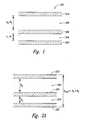
- FIG. 1is a cross-sectional view of an embodiment of the invention.
- FIGS. 2 a - care cross-sectional views of the embodiment of FIG. 1 illustrating the operation thereof.
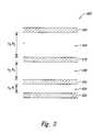
- FIG. 3is a cross-sectional view of another embodiment of the invention.
- FIG. 4is a block diagram of a typical memory device that includes one or more memory arrays of the present embodiment.
- Embodiments of the present inventionprovide a multiple state memory cell. Certain details are set forth below to provide a sufficient understanding of the invention. However, it will be clear to one skilled in the art that the invention may be practiced without these particular details. In other instances, well-known fabrication techniques processing methods, circuits, control signals, and timing protocols have not been shown in detail in order to avoid unnecessarily obscuring the invention.
- FIG. 1Illustrated in FIG. 1 is a cross-sectional view of a portion of a multiple-state memory cell 200 according to an embodiment of the present invention.
- a metal electrode layer 202is formed to provide a cathode layer to which a voltage is applied. It will be appreciated that the metal layer 200 may be formed on a substrate, or on a layer of material which will support the multiple-state memory cell 200 .
- Formed on the metal layer 200is a metal-doped chalcogenide layer 204 through which, as will be explained in more detail below, a conductive link to floating electrode layer 206 is formed under the application of a voltage.
- Chalcogenide materialsinclude those compounds of sulfur, selenium, and tellurium.
- the metal material doping the chalcogenideare generally Group I or Group II metals, such as silver, copper, zinc, and combinations thereof.
- the floating electrode layer 206is typically formed from a metal material, such as silver.
- a another metal-doped chalcogenide layer 208Formed on the floating electrode layer 206 is a another metal-doped chalcogenide layer 208 .
- the composition of the material for layer 208may be, but does not necessarily need to be, the same as the layer 204 . As illustrated in FIG. 2, the thickness t 2 of the layer 208 is greater than the thickness t 1 of the layer 204 . However, in other embodiments of the present invention, the thicknesses t 2 and t 1 may be nearly or approximately the same, or the thickness t 2 may be less than t 1 . As will be explained in more detail below, the composition of the respective metal-doped chalcogenide layers 206 and 208 may need to be modified in order to accommodate layers 206 and 208 having various thicknesses.
- metal-doped chalcogenide layer 208Formed on the metal-doped chalcogenide layer 208 is another metal electrode layer 210 , which represents an anode of the multiple-state memory cell 200 .
- the metal electrode layer 210 and the floating electrode layer 206are typically formed from the same material.
- the cathodeis formed below the anode, however, it will be appreciated that the arrangement of the two layers may be reversed as well without departing from the scope of the present invention.
- the vertical orientation illustrated in FIG. 1can be changed such that the various layers are formed in a horizontal orientation between a cathode and an anode that are laterally spaced apart from one another.
- compositions of germanium selenide, Ge x Se ycan be used. Exemplary ratios are in the range from Ge 20 Se 80 to GeSe. Compositions of arsenic sulfide, germanium telluride, and germanium sulfide can also be used for the metal-doped chalcogenide layers.
- materials that can be used for the electrode layersare also known, such as silver, compositions of silver selenide, copper, germanium selenide, and the like. It will be appreciated that later developed materials that display the same characteristics as known materials can also be used for the metal-doped chalcogenide and electrode layers without deviating from the scope of the present invention.
- the multiple-state memory cell 200 illustrated in FIG. 1is capable of storing multiple states by altering or programming the total resistance between the anode and the cathode in a relatively digital fashion.
- the resistance of the memory cell 200can then measured or compared to determine the value of the data stored by the memory cell 200 .
- multiple statescan be stored by the memory cell 200 .
- the alteration of the resistanceis accomplished by the formation of a conductive growth from the metal electrode layer 202 (ie., the cathode) through the layer 204 to electrically contact the floating electrode layer 206 , and the formation of a conductive growth from the floating electrode layer 206 through the layer 208 to electrically contact the metal electrode layer 210 (ie., the anode).
- the formation of the conductive growthis induced by creating a voltage difference between the cathode and the anode, such as by applying a voltage to the anode and grounding the cathode.
- the resistance between the anode and the cathodechanges relatively significantly.
- the resistance between the anode and the cathode R cellis equal to approximately R 1 +R 2 , where R 1 is the resistance of the layer 204 and R 2 is the resistance of the layer 208 .
- conductive growths 304 and 308begin to form through the layers 204 and 208 , respectively.
- the resistance R cell between the anode and the cathodechanges to a value less than R 1 but greater than a short circuit.
- the resistance R cell at this pointis reproducible, and consequently, can be used to represent a data state.
- the resistance R cellchanges again, as shown in FIG. 2 c, to a relatively low resistance when a conductive growth 304 extends through the layer 204 and creates a short circuit between the cathode, which is represented by the layer 202 , and the floating electrode layer 206 .
- Each of the different resistance states of R cell provided by the memory cell 200represents a different data or logic state. That is, a first data state is represented by R cell being approximately equal to the total resistance (R 1 +R 2 ), a second data state is represented by R cell being a value between R 1 and low resistance, which occurs when the floating electrode layer 206 is short circuited to the metal electrode layer 210 by the conductive growth 308 , and a third data state is represented by a low resistance after the metal electrode layer 202 is short circuited to the floating electrode layer 206 by the conductive growth 304 .
- a reading circuit coupled to the memory cell 200measures the resistance of the memory cell 200 in order to determine the data stored by the cell.
- the growth of the conductive growths 304 and 308is dependent on the orientation of the electrical field applied to the memory cell 200 . That is, as discussed so far, a voltage applied to the metal electrode layer 210 (ie., the anode) is positive relative to the voltage applied to the metal electrode layer 202 (i.e., the cathode), thus, the direction of growth is from the metal electrode layer 202 to the floating electrode layer 206 . Similarly, a conductive growth will be formed extending from the floating electrode layer 206 to the metal electrode layer 210 . However, it will be appreciated that application of the voltage in an opposite polarity will reduce whatever conductive growth has been previously formed. Consequently, the memory cell 200 can be programmed to store a different data state by changing the polarity of the applied voltage to the memory cell 200 during a read or write operation to change the resistance of the memory cell 200 .
- the conductive growth 304eventually creates a short circuit between the cathode and the floating electrode 206 , thus reducing the resistance between the anode and the cathode to a low resistance.
- the resistance R cell across the anode and cathodeis between R 1 and a short circuit after the conductive growth 308 short circuits the floating electrode 206 to the anode 210 because the resistance of the layer 204 is actually reduced as the conductive growth 304 grows toward the floating electrode 206 .
- the resistance R cell at this pointis nevertheless reproducible and different enough from the short circuited state that conventional reading circuits for multiple-state memory cells can consistently recognize the data state.
- the range of resistances, or the transition from one resistance relative to one anothercan be adjusted by altering the thickness of the layers 204 and/or 208 . Additionally, as previously mentioned, the composition of the metal-doped chalcogenide material of the layers 204 and 208 can be adjusted as well to adjust the points of transition in the resistance.
- FIG. 3Illustrated in FIG. 3 is a portion of a memory cell 400 according to another embodiment of the present invention.
- the memory cell 400includes layers that are similar to those of the memory cell 200 (FIG. 1). However, memory cell 400 further includes a second floating electrode 420 and a third metal-doped chalcogenide layer 424 in addition to the layers described with respect to the memory cell 200 . The addition of the second floating electrode 420 and the third metal-doped chalcogenide layer 424 enables the memory cell 400 to have an additional memory state in which to store data.
- the memory cell 400provides four different states or resistances for R cell : (R 3 +R 2 +R 1 ), between (R 2 +R 1 ) and R 1 , between R 1 and low resistance, and low resistance.
- each different resistance levelcan be used to represent a different state of data.
- a memory device 500 that includes a memory array 502 having memory cells according to an embodiment of the inventionis shown in FIG. 4.
- the memory device 500includes a command decoder 506 that receives memory command through a command bus 508 and generates corresponding control signals.
- a row or column addressis applied to the memory device 500 through an address bus 520 and is decoded by a row address decoder 524 or a column address decoder 528 , respectively.
- Memory array read/write circuitry 530are coupled to the array 502 to provide read data to a data output buffer 534 via a input-output data bus 540 . Write data are applied to the memory array through a data input buffer 544 and the memory array read/write circuitry 530 .
Landscapes
- Chemical & Material Sciences (AREA)
- Crystallography & Structural Chemistry (AREA)
- Engineering & Computer Science (AREA)
- Computer Hardware Design (AREA)
- Semiconductor Memories (AREA)
- Static Random-Access Memory (AREA)
- Data Exchanges In Wide-Area Networks (AREA)
Abstract
Description
- The invention relates to random access memories (“RAMs”), and more particularly to memory cells of a RAM capable of storing data in multiple data states.[0001]
- Random access memory devices are an integral part of any computing environment. Without these memory devices, processing data in a computing device would be nearly impossible. Consequently, there has been a great amount of research and development directed to the area of random access computer memory. The research and development has been directed to different areas related to computer memory, for example, in increasing the speed at which data stored by the memory devices can be accessed, in designing memories with lower power consumption, and in engineering memory devices having greater data retention times. Additionally, one particular area to which a great amount of effort has been spent is in the areas of increasing memory density and data capacity.[0002]
- One conventional approach to increasing memory density has been to decrease the size of memory devices, and more particularly, decrease the size of memory cells. As a result, the size of memory cells have been reduced dramatically in the recent past. However, the size of memory cells have diminished to the point where the current state of processing technology is being constantly challenged when manufacturing memory devices with these feature sizes. Another approach to the memory density and data capacity issue has been experiment with memory devices that are capable of storing data in more states than conventional binary memory. That is, conventional memory stores data in a binary format, where data is stored as either one of two different data states. With multiple data state memory, data can be stored as one of many different states, where the number of different states is greater than two. As a result, with multiple data state memory, generally less memory cells need to be used to store data. For example, a memory cell having four different data states can be substituted for two conventional memory cells having only two different data states. Consequently, only half as many memory cells would be needed to store the same quantity of data. Conversely, twice as much data can be stored in the same area if the multiple data state memory is the same size as conventional memory cells.[0003]
- An example of the type of work that has been done in the area of multiple data state memory is provided in several U.S. Patents to Ovshinsky et al. For example, in U.S. Pat. No. 5,296,716 to Ovshinsky et al., the use of electrically writeable and erasable phase change materials for electronic memory applications is described. Additionally, in U.S. Pat. No. 5,912,839 to Ovshinsky et al., a method of programming Ovonic memory multistate-digital multibit memory elements and the use in data storage is described. As described therein, a memory element including the phase change material, that is, materials which can be electrically switched between generally amorphous and generally crystalline, can be programmed by using a number of current pulses. In determining the data state of the memory element, the number of pulses can be discerned by counting the number of pulses required to return the resistance level of the memory element to a first state. The number of pulses represents the data state of the data stored by the memory element. As further described in the aforementioned patent, the process of reading the present state of the memory element is destructive, and consequently, requires that the data is reprogrammed following a read.[0004]
- Another approach that has been taken in the design of multiple data state memory is described in U.S. Patents to Kozicki et al. As described therein, a programmable metallization cell (PMC) formed from a fast ion conductor, such as a chalcogenide material that include compounds containing sulfur, selenium and tellurium, positioned between two electrodes. The formation of a non-volatile metal dendrite can be induced by application of a voltage difference between the two electrodes. The mass of the non-volatile dendrite changes the resistance of the PMC, which can be used as a means to store data in various states. Further described in the aforementioned patents are various structural embodiments of a PMC in different applications.[0005]
- Although there has been development in the area of multiple data state and variable resistance memories, it will be appreciated that new and alternative approaches to this area is still possible. For example, further development in the area of multiple data state memory cells having true quantization of data states. Therefore, there is a need for alternative approaches to storing data in multiple data states.[0006]
- The present invention is directed to a multiple data state memory cell. The memory cell includes a first electrode layer formed from a first conductive material, a second electrode layer formed from a second conductive material, and a first layer of a metal-doped chalcogenide material disposed between the first and second electrode layers, the first layer providing a medium in which a conductive growth can be formed to electrically couple together the first and second electrode layers. The memory cell further includes a third electrode layer formed from a third conductive material, and a second layer of a metal-doped chalcogenide material disposed between the second and third electrode layers, the second layer providing a medium in which a conductive growth can be formed to electrically couple together the second and third electrode layers.[0007]
- FIG. 1 is a cross-sectional view of an embodiment of the invention.[0008]
- FIGS. 2[0009]a-care cross-sectional views of the embodiment of FIG. 1 illustrating the operation thereof.
- FIG. 3 is a cross-sectional view of another embodiment of the invention.[0010]
- FIG. 4 is a block diagram of a typical memory device that includes one or more memory arrays of the present embodiment.[0011]
- As is conventional in the field of integrated circuit representation, the lateral sizes and thicknesses of the various layers are not drawn to scale and may have been enlarged or reduced to improve drawing legibility.[0012]
- Embodiments of the present invention provide a multiple state memory cell. Certain details are set forth below to provide a sufficient understanding of the invention. However, it will be clear to one skilled in the art that the invention may be practiced without these particular details. In other instances, well-known fabrication techniques processing methods, circuits, control signals, and timing protocols have not been shown in detail in order to avoid unnecessarily obscuring the invention.[0013]
- Illustrated in FIG. 1 is a cross-sectional view of a portion of a multiple-[0014]
state memory cell 200 according to an embodiment of the present invention. Ametal electrode layer 202 is formed to provide a cathode layer to which a voltage is applied. It will be appreciated that themetal layer 200 may be formed on a substrate, or on a layer of material which will support the multiple-state memory cell 200. Formed on themetal layer 200 is a metal-dopedchalcogenide layer 204 through which, as will be explained in more detail below, a conductive link to floatingelectrode layer 206 is formed under the application of a voltage. Chalcogenide materials, as referred to herein, include those compounds of sulfur, selenium, and tellurium. The metal material doping the chalcogenide are generally Group I or Group II metals, such as silver, copper, zinc, and combinations thereof. The floatingelectrode layer 206 is typically formed from a metal material, such as silver. - Formed on the[0015]
floating electrode layer 206 is a another metal-dopedchalcogenide layer 208. The composition of the material forlayer 208 may be, but does not necessarily need to be, the same as thelayer 204. As illustrated in FIG. 2, the thickness t2of thelayer 208 is greater than the thickness t1of thelayer 204. However, in other embodiments of the present invention, the thicknesses t2and t1may be nearly or approximately the same, or the thickness t2may be less than t1. As will be explained in more detail below, the composition of the respective metal-dopedchalcogenide layers layers chalcogenide layer 208 is anothermetal electrode layer 210, which represents an anode of the multiple-state memory cell 200. Themetal electrode layer 210 and thefloating electrode layer 206 are typically formed from the same material. As illustrated in FIG. 1, the cathode is formed below the anode, however, it will be appreciated that the arrangement of the two layers may be reversed as well without departing from the scope of the present invention. Moreover, the vertical orientation illustrated in FIG. 1 can be changed such that the various layers are formed in a horizontal orientation between a cathode and an anode that are laterally spaced apart from one another. - It will be appreciated that many materials known by those of ordinary skill in the art may be used for the metal-doped chalcogenide layers. For example, compositions of germanium selenide, Ge[0016]xSey, can be used. Exemplary ratios are in the range from Ge20Se80to GeSe. Compositions of arsenic sulfide, germanium telluride, and germanium sulfide can also be used for the metal-doped chalcogenide layers. Similarly, materials that can be used for the electrode layers are also known, such as silver, compositions of silver selenide, copper, germanium selenide, and the like. It will be appreciated that later developed materials that display the same characteristics as known materials can also be used for the metal-doped chalcogenide and electrode layers without deviating from the scope of the present invention.
- In operation, the multiple-[0017]
state memory cell 200 illustrated in FIG. 1 is capable of storing multiple states by altering or programming the total resistance between the anode and the cathode in a relatively digital fashion. The resistance of thememory cell 200 can then measured or compared to determine the value of the data stored by thememory cell 200. As a result of the relatively discrete manner in which the resistance can be changed, multiple states can be stored by thememory cell 200. - The alteration of the resistance is accomplished by the formation of a conductive growth from the metal electrode layer[0018]202 (ie., the cathode) through the
layer 204 to electrically contact the floatingelectrode layer 206, and the formation of a conductive growth from the floatingelectrode layer 206 through thelayer 208 to electrically contact the metal electrode layer210 (ie., the anode). The formation of the conductive growth is induced by creating a voltage difference between the cathode and the anode, such as by applying a voltage to the anode and grounding the cathode. - Each time a conductive growth creates a short circuit, the resistance between the anode and the cathode changes relatively significantly. Initially, as shown in FIG. 2[0019]a,where no conductive growth has been formed, the resistance between the anode and the cathode Rcellis equal to approximately R1+R2, where R1is the resistance of the
layer 204 and R2is the resistance of thelayer 208. However, under the influence of an applied bias across the metal-doped chalcogenide layers202,210,conductive growths layers conductive growth 308 extends through thelayer 208 and creates a short circuit between the the floatingelectrode layer 206 and the anode, which is represented by thelayer 210, as shown in FIG. 2b,the resistance Rcellbetween the anode and the cathode changes to a value less than R1but greater than a short circuit. The resistance Rcellat this point is reproducible, and consequently, can be used to represent a data state. The resistance Rcellchanges again, as shown in FIG. 2c,to a relatively low resistance when aconductive growth 304 extends through thelayer 204 and creates a short circuit between the cathode, which is represented by thelayer 202, and the floatingelectrode layer 206. - Each of the different resistance states of R[0020]cellprovided by the
memory cell 200 represents a different data or logic state. That is, a first data state is represented by Rcellbeing approximately equal to the total resistance (R1+R2), a second data state is represented by Rcellbeing a value between R1and low resistance, which occurs when the floatingelectrode layer 206 is short circuited to themetal electrode layer 210 by theconductive growth 308, and a third data state is represented by a low resistance after themetal electrode layer 202 is short circuited to the floatingelectrode layer 206 by theconductive growth 304. A reading circuit coupled to thememory cell 200 measures the resistance of thememory cell 200 in order to determine the data stored by the cell. - The growth of the[0021]
conductive growths memory cell 200. That is, as discussed so far, a voltage applied to the metal electrode layer210 (ie., the anode) is positive relative to the voltage applied to the metal electrode layer202 (i.e., the cathode), thus, the direction of growth is from themetal electrode layer 202 to the floatingelectrode layer 206. Similarly, a conductive growth will be formed extending from the floatingelectrode layer 206 to themetal electrode layer 210. However, it will be appreciated that application of the voltage in an opposite polarity will reduce whatever conductive growth has been previously formed. Consequently, thememory cell 200 can be programmed to store a different data state by changing the polarity of the applied voltage to thememory cell 200 during a read or write operation to change the resistance of thememory cell 200. - It will be further appreciated that reading and writing circuitry for use with embodiments of the present invention is well known to those of ordinary skill in the art, and may be implemented using conventional circuitry and design. It will be further appreciated that the description provided herein is sufficient to enable one of ordinary skill in the art to practice the invention.[0022]
- As illustrated in FIG. 2[0023]b,application of a voltage to the anode induces the formation of not only
conductive growth 304, butconductive growth 308 as well. However, because the thickness of thelayer 208 is greater than the thickness of thelayer 204, for a given applied voltage across the multiplestate memory cell 200 the voltage across thelayer 208 is greater than the voltage across thelayer 204. Consequently, the floatingelectrode 206 is short circuited to the anode before the cathode is short circuited to the floatingelectrode 206. With continued application of a voltage to the anode, theconductive growth 304 eventually creates a short circuit between the cathode and the floatingelectrode 206, thus reducing the resistance between the anode and the cathode to a low resistance. Moreover, it will be appreciated that the resistance Rcellacross the anode and cathode is between R1and a short circuit after theconductive growth 308 short circuits the floatingelectrode 206 to theanode 210 because the resistance of thelayer 204 is actually reduced as theconductive growth 304 grows toward the floatingelectrode 206. However, the resistance Rcellat this point is nevertheless reproducible and different enough from the short circuited state that conventional reading circuits for multiple-state memory cells can consistently recognize the data state. - It will be further appreciated that the range of resistances, or the transition from one resistance relative to one another can be adjusted by altering the thickness of the[0024]
layers 204 and/or208. Additionally, as previously mentioned, the composition of the metal-doped chalcogenide material of thelayers - Illustrated in FIG. 3 is a portion of a[0025]
memory cell 400 according to another embodiment of the present invention. Thememory cell 400 includes layers that are similar to those of the memory cell200 (FIG. 1). However,memory cell 400 further includes a second floatingelectrode 420 and a third metal-dopedchalcogenide layer 424 in addition to the layers described with respect to thememory cell 200. The addition of the second floatingelectrode 420 and the third metal-dopedchalcogenide layer 424 enables thememory cell 400 to have an additional memory state in which to store data. That is, whereas thememory cell 200 provides three different states or resistances Rcell: (R2+R1), between R1and low resistance, and low resistance, thememory cell 400 provides four different states or resistances for Rcell: (R3+R2+R1), between (R2+R1) and R1, between R1and low resistance, and low resistance. As previously discussed, each different resistance level can be used to represent a different state of data. - As illustrated by the previous discussion, it will be appreciated that including additional layers formed from a metal-doped chalcogenide material and a floating electrode can be used to create memory cells having even more states than that provided by the[0026]
memory cell 400. - A[0027]
memory device 500 that includes amemory array 502 having memory cells according to an embodiment of the invention is shown in FIG. 4. Thememory device 500 includes acommand decoder 506 that receives memory command through acommand bus 508 and generates corresponding control signals. A row or column address is applied to thememory device 500 through anaddress bus 520 and is decoded by arow address decoder 524 or acolumn address decoder 528, respectively. Memory array read/write circuitry 530 are coupled to thearray 502 to provide read data to a data output buffer534 via a input-output data bus 540. Write data are applied to the memory array through a data input buffer544 and the memory array read/write circuitry 530. - From the foregoing it will be appreciated that, although specific embodiments of the invention have been described herein for purposes of illustration, various modifications may be made without deviating from the spirit and scope of the invention. Accordingly, the invention is not limited except as by the appended claims.[0028]
Claims (24)
1-10. (cancelled)
11. A multiple-state memory cell, comprising:
a first electrode coupled to a first voltage;
a second electrode coupled to a second voltage;
a multiple layer data state stack in which multiple data states are stored, the data-state stack including:
a first portion of a metal-doped chalcogenide material adjoining the first electrode, the first portion having a first thickness;
a third electrode of a conductive material adjoining the first portion; and
a second portion of a metal-doped chalcogenide material adjoining the third electrode, the second portion having a second thickness,
wherein application of a programming voltage to the first electrode induces the formation of a first conductive growth from the third electrode to the first electrode and a second conductive growth from the second electrode to the third electrode.
12. The memory cell ofclaim 11 wherein the first voltage is positive relative to the second voltage.
13. The memory cell ofclaim 11 wherein the first voltage is negative relative to the second voltage.
14. The memory cell ofclaim 11 wherein the first portion is positioned below the third electrode, and the third electrode is positioned below the second portion.
15. The memory cell ofclaim 11 wherein the first portion is positioned laterally adjacent to the third electrode, and the third electrode is positioned laterally adjacent to the second portion.
16. The memory cell ofclaim 11 wherein the first thickness is less than the second thickness.
17. The memory cell ofclaim 11 wherein under the application of the programming voltage, the first conductive growth couples the third electrode to the first electrode prior to the second conductive growth coupling the second electrode to the third electrode.
18-41. (cancelled).
42. A method of storing multiple data states in a memory, comprising:
storing a first data state, short circuiting a first electrode to a second electrode to change a resistance from an initial resistance to a first resistance;
storing a data state, short circuiting the second electrode to a third electrode to change the first resistance to a second resistance; and
storing a third data state, substantially maintaining the initial resistance between the first and second electrodes and the second and third electrodes.
43. The method ofclaim 42 wherein short circuiting the first electrode to a second electrode comprises applying a programming voltage to induce the formation of a conductive growth from the first electrode that couples the first electrode to the second electrode and wherein short circuiting the second electrode to the third electrode comprises applying the programming voltage to induce the formation of a conductive growth from the second electrode that couples the second electrode to the third electrode.
44. The method ofclaim 43 wherein under the application of the programming voltage the first electrode is short circuited to the second electrode prior to the second electrode short circuiting to the third electrode.
45. The method ofclaim 42 , further comprising to store a fourth data state, short circuiting the third electrode to a fourth electrode to change the second resistance to a third resistance.
46. A method for forming a multiple state memory cell, comprising:
forming a first electrode layer from a first conductive material;
forming a first layer from a metal-doped conductive material on the first electrode layer;
forming a second electrode layer from a second conductive material on the first layer;
forming a second layer from a metal-doped chalcogenide material on the second layer;
forming a third electrode layer from a third conductive material on the second layer;
the first layer providing a medium in which a conductive growth can be formed to electrically couple together the first and second electrode layers and the second layer providing a medium in which a conductive growth can be formed to electrically couple together the second and third electrode layers.
47. The method of claim1 wherein forming the first electrode layer comprises forming the first electrode layer from a composition of a silver material.
48. The method of claim1 wherein forming the first and second electrode layers comprises forming the first and second electrodes from the same type of material.
49. The method of claim1 wherein forming the first layer and forming the second layer comprises forming the first layer having a thickness less than the thickness of the second layer.
50. The method of claim1 wherein forming the first layer and forming the second layer comprises forming the first layer having a thickness less than the thickness of the second layer.
51. The method of claim1, further comprising:
forming a third layer of a metal-doped chalcogenide material on the third electrode layer; and
forming a fourth electrode formed from a fourth conductive material on the third layer, the third layer providing a medium in which a conductive growth can be formed to electrically couple together the third and fourth electrode layers.
52. The method of claim1 wherein the metal-doped chalcogenide material of the first and second layers are the same.
53. The method of claim1 wherein the metal-doped chalcogenide material of at least one of the first and second layers comprises a material selected from the group consisting of germanium selenide, arsenic sulfide, germanium telluride, and germanium sulfide.
54. The method of claim1 wherein the metal-doped chalcogenide material of at least one of the first and second layers comprises a composition of germanium selenide.
55. The method of claim1 wherein the first electrode is formed beneath the first layer, the first layer is formed beneath the second electrode, the second electrode is formed beneath the second layer, and the second layer is formed beneath the third electrode layer.
56. The method of claim1 wherein the first electrode is formed adjacent the first layer, the first layer is formed adjacent the second electrode, the second electrode is formed adjacent the second layer, and the second layer is formed adjacent the third electrode layer.
Priority Applications (3)
| Application Number | Priority Date | Filing Date | Title |
|---|---|---|---|
| US10/864,419US6908808B2 (en) | 2002-02-20 | 2004-06-10 | Method of forming and storing data in a multiple state memory cell |
| US11/080,442US7202520B2 (en) | 2002-02-20 | 2005-03-16 | Multiple data state memory cell |
| US11/700,086US7498231B2 (en) | 2002-02-20 | 2007-01-31 | Multiple data state memory cell |
Applications Claiming Priority (2)
| Application Number | Priority Date | Filing Date | Title |
|---|---|---|---|
| US10/081,594US6809362B2 (en) | 2002-02-20 | 2002-02-20 | Multiple data state memory cell |
| US10/864,419US6908808B2 (en) | 2002-02-20 | 2004-06-10 | Method of forming and storing data in a multiple state memory cell |
Related Parent Applications (1)
| Application Number | Title | Priority Date | Filing Date |
|---|---|---|---|
| US10/081,594DivisionUS6809362B2 (en) | 2002-02-20 | 2002-02-20 | Multiple data state memory cell |
Related Child Applications (1)
| Application Number | Title | Priority Date | Filing Date |
|---|---|---|---|
| US11/080,442DivisionUS7202520B2 (en) | 2002-02-20 | 2005-03-16 | Multiple data state memory cell |
Publications (2)
| Publication Number | Publication Date |
|---|---|
| US20040223357A1true US20040223357A1 (en) | 2004-11-11 |
| US6908808B2 US6908808B2 (en) | 2005-06-21 |
Family
ID=27733281
Family Applications (4)
| Application Number | Title | Priority Date | Filing Date |
|---|---|---|---|
| US10/081,594Expired - LifetimeUS6809362B2 (en) | 2002-02-20 | 2002-02-20 | Multiple data state memory cell |
| US10/864,419Expired - LifetimeUS6908808B2 (en) | 2002-02-20 | 2004-06-10 | Method of forming and storing data in a multiple state memory cell |
| US11/080,442Expired - LifetimeUS7202520B2 (en) | 2002-02-20 | 2005-03-16 | Multiple data state memory cell |
| US11/700,086Expired - LifetimeUS7498231B2 (en) | 2002-02-20 | 2007-01-31 | Multiple data state memory cell |
Family Applications Before (1)
| Application Number | Title | Priority Date | Filing Date |
|---|---|---|---|
| US10/081,594Expired - LifetimeUS6809362B2 (en) | 2002-02-20 | 2002-02-20 | Multiple data state memory cell |
Family Applications After (2)
| Application Number | Title | Priority Date | Filing Date |
|---|---|---|---|
| US11/080,442Expired - LifetimeUS7202520B2 (en) | 2002-02-20 | 2005-03-16 | Multiple data state memory cell |
| US11/700,086Expired - LifetimeUS7498231B2 (en) | 2002-02-20 | 2007-01-31 | Multiple data state memory cell |
Country Status (10)
| Country | Link |
|---|---|
| US (4) | US6809362B2 (en) |
| EP (1) | EP1476876B1 (en) |
| JP (1) | JP2005518671A (en) |
| KR (1) | KR100635366B1 (en) |
| CN (2) | CN100449644C (en) |
| AT (1) | ATE358876T1 (en) |
| AU (1) | AU2003212907A1 (en) |
| DE (1) | DE60312961T2 (en) |
| TW (1) | TW587347B (en) |
| WO (1) | WO2003073428A1 (en) |
Cited By (3)
| Publication number | Priority date | Publication date | Assignee | Title |
|---|---|---|---|---|
| US20080037324A1 (en)* | 2006-08-14 | 2008-02-14 | Geoffrey Wen-Tai Shuy | Electrical thin film memory |
| US20080286955A1 (en)* | 2007-05-14 | 2008-11-20 | Geoffrey Wen-Tai Shuy | Fabrication of Recordable Electrical Memory |
| US20090067230A1 (en)* | 2007-09-11 | 2009-03-12 | Samsung Electronics Co., Ltd. | Multi-level memory devices and methods of operating the same |
Families Citing this family (53)
| Publication number | Priority date | Publication date | Assignee | Title |
|---|---|---|---|---|
| US6864521B2 (en)* | 2002-08-29 | 2005-03-08 | Micron Technology, Inc. | Method to control silver concentration in a resistance variable memory element |
| US7227170B2 (en)* | 2003-03-10 | 2007-06-05 | Energy Conversion Devices, Inc. | Multiple bit chalcogenide storage device |
| US7381611B2 (en)* | 2003-08-04 | 2008-06-03 | Intel Corporation | Multilayered phase change memory |
| US7471552B2 (en)* | 2003-08-04 | 2008-12-30 | Ovonyx, Inc. | Analog phase change memory |
| US7529123B2 (en)* | 2003-09-08 | 2009-05-05 | Ovonyx, Inc. | Method of operating a multi-terminal electronic device |
| JP4608875B2 (en)* | 2003-12-03 | 2011-01-12 | ソニー株式会社 | Storage device |
| US7326950B2 (en) | 2004-07-19 | 2008-02-05 | Micron Technology, Inc. | Memory device with switching glass layer |
| US7190048B2 (en) | 2004-07-19 | 2007-03-13 | Micron Technology, Inc. | Resistance variable memory device and method of fabrication |
| WO2006132813A1 (en)* | 2004-07-19 | 2006-12-14 | Micron Technology, Inc. | Memory device with switching glass layer |
| US20060045974A1 (en)* | 2004-08-25 | 2006-03-02 | Campbell Kristy A | Wet chemical method to form silver-rich silver-selenide |
| EP1643508B1 (en)* | 2004-10-01 | 2013-05-22 | International Business Machines Corporation | Non-volatile memory element with programmable resistance |
| JP2006108645A (en)* | 2004-10-08 | 2006-04-20 | Ind Technol Res Inst | Multi-level phase change memory, its operating method and manufacturing method |
| TWI254443B (en)* | 2004-10-08 | 2006-05-01 | Ind Tech Res Inst | Multilevel phase-change memory, manufacture method and status transferring method thereof |
| DE102004052645A1 (en)* | 2004-10-29 | 2006-05-04 | Infineon Technologies Ag | Non-volatile (sic) resistive storage cell with solid electrolyte matrix between first and second electrode as active layer useful in semiconductor technology has elements from groups IVb and Vb and transition metals in active layer |
| US7138290B2 (en)* | 2004-12-03 | 2006-11-21 | Micron Technology, Inc. | Methods of depositing silver onto a metal selenide-comprising surface and methods of depositing silver onto a selenium-comprising surface |
| US8193606B2 (en)* | 2005-02-28 | 2012-06-05 | Semiconductor Energy Laboratory Co., Ltd. | Semiconductor device including a memory element |
| KR100657956B1 (en)* | 2005-04-06 | 2006-12-14 | 삼성전자주식회사 | Multi-value resistor memory device and its manufacture and operation method |
| US7427770B2 (en)* | 2005-04-22 | 2008-09-23 | Micron Technology, Inc. | Memory array for increased bit density |
| US20070009821A1 (en)* | 2005-07-08 | 2007-01-11 | Charlotte Cutler | Devices containing multi-bit data |
| US20080042119A1 (en)* | 2005-08-09 | 2008-02-21 | Ovonyx, Inc. | Multi-layered chalcogenide and related devices having enhanced operational characteristics |
| US7723712B2 (en)* | 2006-03-17 | 2010-05-25 | Micron Technology, Inc. | Reduced power consumption phase change memory and methods for forming the same |
| US7479671B2 (en)* | 2006-08-29 | 2009-01-20 | International Business Machines Corporation | Thin film phase change memory cell formed on silicon-on-insulator substrate |
| US7560723B2 (en) | 2006-08-29 | 2009-07-14 | Micron Technology, Inc. | Enhanced memory density resistance variable memory cells, arrays, devices and systems including the same, and methods of fabrication |
| US20080152792A1 (en)* | 2006-12-21 | 2008-06-26 | Motorola, Inc. | Method of manufacturing a bistable microelectronic switch stack |
| US7705707B2 (en)* | 2006-12-21 | 2010-04-27 | Motorola, Inc. | Bistable microelectronic switch stack |
| US20080165569A1 (en)* | 2007-01-04 | 2008-07-10 | Chieh-Fang Chen | Resistance Limited Phase Change Memory Material |
| KR100810617B1 (en) | 2007-02-09 | 2008-03-06 | 삼성전자주식회사 | Multi-bit phase change memory device and manufacturing method |
| KR20080088776A (en)* | 2007-03-30 | 2008-10-06 | 삼성전자주식회사 | Storage of nonvolatile memory and its formation method |
| KR100941514B1 (en) | 2007-04-06 | 2010-02-12 | 삼성전자주식회사 | Multi-bit phase change memory device and manufacturing method |
| DE102007032865A1 (en)* | 2007-07-13 | 2009-01-15 | Qimonda Ag | Integrated circuit for resistivity changing devices, has memory cell, which comprises two resistivity changing layers stacked one above other, in which each resistivity changing layer serves as separate data storage layer |
| US20090135640A1 (en)* | 2007-11-28 | 2009-05-28 | International Business Machines Corporation | Electromigration-programmable semiconductor device with bidirectional resistance change |
| US7786463B2 (en)* | 2008-05-20 | 2010-08-31 | Seagate Technology Llc | Non-volatile multi-bit memory with programmable capacitance |
| US7977722B2 (en)* | 2008-05-20 | 2011-07-12 | Seagate Technology Llc | Non-volatile memory with programmable capacitance |
| US8742387B2 (en)* | 2008-06-25 | 2014-06-03 | Qimonda Ag | Resistive memory devices with improved resistive changing elements |
| US7825479B2 (en) | 2008-08-06 | 2010-11-02 | International Business Machines Corporation | Electrical antifuse having a multi-thickness dielectric layer |
| US8487291B2 (en)* | 2009-01-30 | 2013-07-16 | Seagate Technology Llc | Programmable metallization memory cell with layered solid electrolyte structure |
| US8331168B2 (en) | 2009-04-30 | 2012-12-11 | International Business Machines Corporation | Increased capacity heterogeneous storage elements |
| US8134139B2 (en)* | 2010-01-25 | 2012-03-13 | Macronix International Co., Ltd. | Programmable metallization cell with ion buffer layer |
| JP2011204744A (en)* | 2010-03-24 | 2011-10-13 | Toshiba Corp | Semiconductor memory device |
| US8828788B2 (en)* | 2010-05-11 | 2014-09-09 | Micron Technology, Inc. | Forming electrodes for chalcogenide containing devices |
| US8395926B2 (en)* | 2010-06-18 | 2013-03-12 | Sandisk 3D Llc | Memory cell with resistance-switching layers and lateral arrangement |
| US8520425B2 (en) | 2010-06-18 | 2013-08-27 | Sandisk 3D Llc | Resistive random access memory with low current operation |
| US8724369B2 (en) | 2010-06-18 | 2014-05-13 | Sandisk 3D Llc | Composition of memory cell with resistance-switching layers |
| JP5364739B2 (en) | 2011-02-18 | 2013-12-11 | 株式会社東芝 | Nonvolatile resistance change element |
| JP2012199336A (en) | 2011-03-18 | 2012-10-18 | Sony Corp | Memory element and memory device |
| JP5687978B2 (en)* | 2011-09-14 | 2015-03-25 | ルネサスエレクトロニクス株式会社 | Resistance variable nonvolatile memory device, semiconductor device, and resistance variable nonvolatile memory operating method |
| CN102306705A (en)* | 2011-09-16 | 2012-01-04 | 北京大学 | A large-capacity multi-value resistive memory |
| CN103078053A (en)* | 2012-12-21 | 2013-05-01 | 北京大学 | Multi-value resistive random access memory (RRAM) and manufacturing method thereof |
| US9416949B2 (en)* | 2013-01-25 | 2016-08-16 | Field Controls, Llc | Adjustable bracket assembly for an ultraviolet lamp |
| US20160005965A1 (en)* | 2014-07-01 | 2016-01-07 | Micron Technology, Inc. | Memory cells having a first selecting chalcogenide material and a second selecting chalcogenide material and methods therof |
| US9406881B1 (en) | 2015-04-24 | 2016-08-02 | Micron Technology, Inc. | Memory cells having a heater electrode formed between a first storage material and a second storage material and methods of forming the same |
| US10008665B1 (en)* | 2016-12-27 | 2018-06-26 | Intel Corporation | Doping of selector and storage materials of a memory cell |
| US11444125B2 (en)* | 2020-06-17 | 2022-09-13 | Globalfoundries Singapore Pte. Ltd. | Memory devices and methods of forming memory devices |
Citations (94)
| Publication number | Priority date | Publication date | Assignee | Title |
|---|---|---|---|---|
| US32254A (en)* | 1861-05-07 | Improvement in methods of distillation | ||
| US38301A (en)* | 1863-04-28 | Improved alloys of aluminum | ||
| US47772A (en)* | 1865-05-16 | Improvement in grain-separators | ||
| US47773A (en)* | 1865-05-16 | Chakles k | ||
| US47765A (en)* | 1865-05-16 | Improved metallic thill-holder | ||
| US137869A (en)* | 1873-04-15 | Improvement in stilts | ||
| US160551A (en)* | 1875-03-09 | Improvement in revolving fire-arfvls | ||
| US190289A (en)* | 1877-05-01 | Improvement in sewing-machine shuttles | ||
| US3961314A (en)* | 1974-03-05 | 1976-06-01 | Energy Conversion Devices, Inc. | Structure and method for producing an image |
| US3966317A (en)* | 1974-04-08 | 1976-06-29 | Energy Conversion Devices, Inc. | Dry process production of archival microform records from hard copy |
| US4267261A (en)* | 1971-07-15 | 1981-05-12 | Energy Conversion Devices, Inc. | Method for full format imaging |
| US4269935A (en)* | 1979-07-13 | 1981-05-26 | Ionomet Company, Inc. | Process of doping silver image in chalcogenide layer |
| US4312938A (en)* | 1979-07-06 | 1982-01-26 | Drexler Technology Corporation | Method for making a broadband reflective laser recording and data storage medium with absorptive underlayer |
| US4316946A (en)* | 1979-12-03 | 1982-02-23 | Ionomet Company, Inc. | Surface sensitized chalcogenide product and process for making and using the same |
| US4320191A (en)* | 1978-11-07 | 1982-03-16 | Nippon Telegraph & Telephone Public Corporation | Pattern-forming process |
| US4499557A (en)* | 1980-10-28 | 1985-02-12 | Energy Conversion Devices, Inc. | Programmable cell for use in programmable electronic arrays |
| US4637895A (en)* | 1985-04-01 | 1987-01-20 | Energy Conversion Devices, Inc. | Gas mixtures for the vapor deposition of semiconductor material |
| US4646266A (en)* | 1984-09-28 | 1987-02-24 | Energy Conversion Devices, Inc. | Programmable semiconductor structures and methods for using the same |
| US4664939A (en)* | 1985-04-01 | 1987-05-12 | Energy Conversion Devices, Inc. | Vertical semiconductor processor |
| US4668968A (en)* | 1984-05-14 | 1987-05-26 | Energy Conversion Devices, Inc. | Integrated circuit compatible thin film field effect transistor and method of making same |
| US4670763A (en)* | 1984-05-14 | 1987-06-02 | Energy Conversion Devices, Inc. | Thin film field effect transistor |
| US4671618A (en)* | 1986-05-22 | 1987-06-09 | Wu Bao Gang | Liquid crystalline-plastic material having submillisecond switch times and extended memory |
| US4728406A (en)* | 1986-08-18 | 1988-03-01 | Energy Conversion Devices, Inc. | Method for plasma - coating a semiconductor body |
| US4737379A (en)* | 1982-09-24 | 1988-04-12 | Energy Conversion Devices, Inc. | Plasma deposited coatings, and low temperature plasma method of making same |
| US4795657A (en)* | 1984-04-13 | 1989-01-03 | Energy Conversion Devices, Inc. | Method of fabricating a programmable array |
| US4800526A (en)* | 1987-05-08 | 1989-01-24 | Gaf Corporation | Memory element for information storage and retrieval system and associated process |
| US4809044A (en)* | 1986-08-22 | 1989-02-28 | Energy Conversion Devices, Inc. | Thin film overvoltage protection devices |
| US4818717A (en)* | 1986-06-27 | 1989-04-04 | Energy Conversion Devices, Inc. | Method for making electronic matrix arrays |
| US4891330A (en)* | 1987-07-27 | 1990-01-02 | Energy Conversion Devices, Inc. | Method of fabricating n-type and p-type microcrystalline semiconductor alloy material including band gap widening elements |
| US5177567A (en)* | 1991-07-19 | 1993-01-05 | Energy Conversion Devices, Inc. | Thin-film structure for chalcogenide electrical switching devices and process therefor |
| US5296716A (en)* | 1991-01-18 | 1994-03-22 | Energy Conversion Devices, Inc. | Electrically erasable, directly overwritable, multibit single cell memory elements and arrays fabricated therefrom |
| US5314772A (en)* | 1990-10-09 | 1994-05-24 | Arizona Board Of Regents | High resolution, multi-layer resist for microlithography and method therefor |
| US5315131A (en)* | 1990-11-22 | 1994-05-24 | Matsushita Electric Industrial Co., Ltd. | Electrically reprogrammable nonvolatile memory device |
| US5406509A (en)* | 1991-01-18 | 1995-04-11 | Energy Conversion Devices, Inc. | Electrically erasable, directly overwritable, multibit single cell memory elements and arrays fabricated therefrom |
| US5414271A (en)* | 1991-01-18 | 1995-05-09 | Energy Conversion Devices, Inc. | Electrically erasable memory elements having improved set resistance stability |
| US5500532A (en)* | 1994-08-18 | 1996-03-19 | Arizona Board Of Regents | Personal electronic dosimeter |
| US5512328A (en)* | 1992-08-07 | 1996-04-30 | Hitachi, Ltd. | Method for forming a pattern and forming a thin film used in pattern formation |
| US5512773A (en)* | 1993-12-23 | 1996-04-30 | U.S. Philips Corporation | Switching element with memory provided with Schottky tunnelling barrier |
| US5591501A (en)* | 1995-12-20 | 1997-01-07 | Energy Conversion Devices, Inc. | Optical recording medium having a plurality of discrete phase change data recording points |
| US5596522A (en)* | 1991-01-18 | 1997-01-21 | Energy Conversion Devices, Inc. | Homogeneous compositions of microcrystalline semiconductor material, semiconductor devices and directly overwritable memory elements fabricated therefrom, and arrays fabricated from the memory elements |
| US5714768A (en)* | 1995-10-24 | 1998-02-03 | Energy Conversion Devices, Inc. | Second-layer phase change memory array on top of a logic device |
| US5726083A (en)* | 1994-11-29 | 1998-03-10 | Nec Corporation | Process of fabricating dynamic random access memory device having storage capacitor low in contact resistance and small in leakage current through tantalum oxide film |
| US5751012A (en)* | 1995-06-07 | 1998-05-12 | Micron Technology, Inc. | Polysilicon pillar diode for use in a non-volatile memory cell |
| US5869843A (en)* | 1995-06-07 | 1999-02-09 | Micron Technology, Inc. | Memory array having a multi-state element and method for forming such array or cells thereof |
| US5896312A (en)* | 1996-05-30 | 1999-04-20 | Axon Technologies Corporation | Programmable metallization cell structure and method of making same |
| US6011757A (en)* | 1998-01-27 | 2000-01-04 | Ovshinsky; Stanford R. | Optical recording media having increased erasability |
| US6031287A (en)* | 1997-06-18 | 2000-02-29 | Micron Technology, Inc. | Contact structure and memory element incorporating the same |
| US6177338B1 (en)* | 1999-02-08 | 2001-01-23 | Taiwan Semiconductor Manufacturing Company | Two step barrier process |
| US6236059B1 (en)* | 1996-08-22 | 2001-05-22 | Micron Technology, Inc. | Memory cell incorporating a chalcogenide element and method of making same |
| US20020000666A1 (en)* | 1998-08-31 | 2002-01-03 | Michael N. Kozicki | Self-repairing interconnections for electrical circuits |
| US6339544B1 (en)* | 2000-09-29 | 2002-01-15 | Intel Corporation | Method to enhance performance of thermal resistor device |
| US6348365B1 (en)* | 2001-03-02 | 2002-02-19 | Micron Technology, Inc. | PCRAM cell manufacturing |
| US6350679B1 (en)* | 1999-08-03 | 2002-02-26 | Micron Technology, Inc. | Methods of providing an interlevel dielectric layer intermediate different elevation conductive metal layers in the fabrication of integrated circuitry |
| US6376284B1 (en)* | 1996-02-23 | 2002-04-23 | Micron Technology, Inc. | Method of fabricating a memory device |
| US6391688B1 (en)* | 1995-06-07 | 2002-05-21 | Micron Technology, Inc. | Method for fabricating an array of ultra-small pores for chalcogenide memory cells |
| US20030001229A1 (en)* | 2001-03-01 | 2003-01-02 | Moore John T. | Chalcogenide comprising device |
| US6507061B1 (en)* | 2001-08-31 | 2003-01-14 | Intel Corporation | Multiple layer phase-change memory |
| US6511862B2 (en)* | 2001-06-30 | 2003-01-28 | Ovonyx, Inc. | Modified contact for programmable devices |
| US6512241B1 (en)* | 2001-12-31 | 2003-01-28 | Intel Corporation | Phase change material memory device |
| US6511867B2 (en)* | 2001-06-30 | 2003-01-28 | Ovonyx, Inc. | Utilizing atomic layer deposition for programmable device |
| US6514805B2 (en)* | 2001-06-30 | 2003-02-04 | Intel Corporation | Trench sidewall profile for device isolation |
| US20030027416A1 (en)* | 2001-08-01 | 2003-02-06 | Moore John T. | Method of forming integrated circuitry, method of forming memory circuitry, and method of forming random access memory circuitry |
| US20030032254A1 (en)* | 2000-12-08 | 2003-02-13 | Gilton Terry L. | Resistance variable device, analog memory device, and programmable memory cell |
| US20030035314A1 (en)* | 1998-12-04 | 2003-02-20 | Kozicki Michael N. | Programmable microelectronic devices and methods of forming and programming same |
| US20030035315A1 (en)* | 2001-04-06 | 2003-02-20 | Kozicki Michael N. | Microelectronic device, structure, and system, including a memory structure having a variable programmable property and method of forming the same |
| US20030038301A1 (en)* | 2001-08-27 | 2003-02-27 | John Moore | Apparatus and method for dual cell common electrode PCRAM memory device |
| US20030045054A1 (en)* | 2001-08-29 | 2003-03-06 | Campbell Kristy A. | Method of forming non-volatile resistance variable devices, method of forming a programmable memory cell of memory circuitry, and a non-volatile resistance variable device |
| US20030043631A1 (en)* | 2001-08-30 | 2003-03-06 | Gilton Terry L. | Method of retaining memory state in a programmable conductor RAM |
| US20030045049A1 (en)* | 2001-08-29 | 2003-03-06 | Campbell Kristy A. | Method of forming chalcogenide comprising devices |
| US6531373B2 (en)* | 2000-12-27 | 2003-03-11 | Ovonyx, Inc. | Method of forming a phase-change memory cell using silicon on insulator low electrode in charcogenide elements |
| US20030049912A1 (en)* | 2001-08-29 | 2003-03-13 | Campbell Kristy A. | Method of forming chalcogenide comprsing devices and method of forming a programmable memory cell of memory circuitry |
| US20030048744A1 (en)* | 2001-09-01 | 2003-03-13 | Ovshinsky Stanford R. | Increased data storage in optical data storage and retrieval systems using blue lasers and/or plasmon lenses |
| US20030047765A1 (en)* | 2001-08-30 | 2003-03-13 | Campbell Kristy A. | Stoichiometry for chalcogenide glasses useful for memory devices and method of formation |
| US20030047773A1 (en)* | 2001-03-15 | 2003-03-13 | Jiutao Li | Agglomeration elimination for metal sputter deposition of chalcogenides |
| US20030048519A1 (en)* | 2000-02-11 | 2003-03-13 | Kozicki Michael N. | Microelectronic photonic structure and device and method of forming the same |
| US6534781B2 (en)* | 2000-12-26 | 2003-03-18 | Ovonyx, Inc. | Phase-change memory bipolar array utilizing a single shallow trench isolation for creating an individual active area region for two memory array elements and one bipolar base contact |
| US6545287B2 (en)* | 2001-09-07 | 2003-04-08 | Intel Corporation | Using selective deposition to form phase-change memory cells |
| US6545907B1 (en)* | 2001-10-30 | 2003-04-08 | Ovonyx, Inc. | Technique and apparatus for performing write operations to a phase change material memory device |
| US20030068861A1 (en)* | 2001-08-30 | 2003-04-10 | Jiutao Li | Integrated circuit device and fabrication using metal-doped chalcogenide materials |
| US6555860B2 (en)* | 2000-09-29 | 2003-04-29 | Intel Corporation | Compositionally modified resistive electrode |
| US6563164B2 (en)* | 2000-09-29 | 2003-05-13 | Ovonyx, Inc. | Compositionally modified resistive electrode |
| US6567293B1 (en)* | 2000-09-29 | 2003-05-20 | Ovonyx, Inc. | Single level metal memory cell using chalcogenide cladding |
| US6566700B2 (en)* | 2001-10-11 | 2003-05-20 | Ovonyx, Inc. | Carbon-containing interfacial layer for phase-change memory |
| US20030096497A1 (en)* | 2001-11-19 | 2003-05-22 | Micron Technology, Inc. | Electrode structure for use in an integrated circuit |
| US20030095426A1 (en)* | 2001-11-20 | 2003-05-22 | Glen Hush | Complementary bit PCRAM sense amplifier and method of operation |
| US6569705B2 (en)* | 2000-12-21 | 2003-05-27 | Intel Corporation | Metal structure for a phase-change memory device |
| US6570784B2 (en)* | 2001-06-29 | 2003-05-27 | Ovonyx, Inc. | Programming a phase-change material memory |
| US6673700B2 (en)* | 2001-06-30 | 2004-01-06 | Ovonyx, Inc. | Reduced area intersection between electrode and programming element |
| US6687427B2 (en)* | 2000-12-29 | 2004-02-03 | Intel Corporation | Optic switch |
| US6690026B2 (en)* | 2001-09-28 | 2004-02-10 | Intel Corporation | Method of fabricating a three-dimensional array of active media |
| US6696355B2 (en)* | 2000-12-14 | 2004-02-24 | Ovonyx, Inc. | Method to selectively increase the top resistance of the lower programming electrode in a phase-change memory |
| US20040035401A1 (en)* | 2002-08-26 | 2004-02-26 | Subramanian Ramachandran | Hydrogen powered scooter |
| US6707712B2 (en)* | 2001-08-02 | 2004-03-16 | Intel Corporation | Method for reading a structural phase-change memory |
| US6714954B2 (en)* | 2002-05-10 | 2004-03-30 | Energy Conversion Devices, Inc. | Methods of factoring and modular arithmetic |
Family Cites Families (112)
| Publication number | Priority date | Publication date | Assignee | Title |
|---|---|---|---|---|
| US3271591A (en) | 1963-09-20 | 1966-09-06 | Energy Conversion Devices Inc | Symmetrical current controlling device |
| US3622319A (en) | 1966-10-20 | 1971-11-23 | Western Electric Co | Nonreflecting photomasks and methods of making same |
| US3868651A (en) | 1970-08-13 | 1975-02-25 | Energy Conversion Devices Inc | Method and apparatus for storing and reading data in a memory having catalytic material to initiate amorphous to crystalline change in memory structure |
| US3743847A (en) | 1971-06-01 | 1973-07-03 | Motorola Inc | Amorphous silicon film as a uv filter |
| US4177474A (en) | 1977-05-18 | 1979-12-04 | Energy Conversion Devices, Inc. | High temperature amorphous semiconductor member and method of making the same |
| US4269395A (en)* | 1978-07-23 | 1981-05-26 | Newman James L | Portable hydraulic rig for performing workover, drilling and other operations on a well |
| DE2901303C2 (en) | 1979-01-15 | 1984-04-19 | Max Planck Gesellschaft Zur Foerderung Der Wissenschaften E.V., 3400 Goettingen | Solid ionic conductor material, its use and process for its manufacture |
| JPS6024580B2 (en) | 1980-03-10 | 1985-06-13 | 日本電信電話株式会社 | Manufacturing method for semiconductor devices |
| US4405710A (en) | 1981-06-22 | 1983-09-20 | Cornell Research Foundation, Inc. | Ion beam exposure of (g-Gex -Se1-x) inorganic resists |
| US4545111A (en) | 1983-01-18 | 1985-10-08 | Energy Conversion Devices, Inc. | Method for making, parallel preprogramming or field programming of electronic matrix arrays |
| US4608296A (en) | 1983-12-06 | 1986-08-26 | Energy Conversion Devices, Inc. | Superconducting films and devices exhibiting AC to DC conversion |
| US4673957A (en) | 1984-05-14 | 1987-06-16 | Energy Conversion Devices, Inc. | Integrated circuit compatible thin film field effect transistor and method of making same |
| US4843443A (en) | 1984-05-14 | 1989-06-27 | Energy Conversion Devices, Inc. | Thin film field effect transistor and method of making same |
| US4769338A (en) | 1984-05-14 | 1988-09-06 | Energy Conversion Devices, Inc. | Thin film field effect transistor and method of making same |
| US4678679A (en) | 1984-06-25 | 1987-07-07 | Energy Conversion Devices, Inc. | Continuous deposition of activated process gases |
| US4710899A (en) | 1985-06-10 | 1987-12-01 | Energy Conversion Devices, Inc. | Data storage medium incorporating a transition metal for increased switching speed |
| US4766471A (en) | 1986-01-23 | 1988-08-23 | Energy Conversion Devices, Inc. | Thin film electro-optical devices |
| US4845533A (en) | 1986-08-22 | 1989-07-04 | Energy Conversion Devices, Inc. | Thin film electrical devices with amorphous carbon electrodes and method of making same |
| US4853785A (en) | 1986-10-15 | 1989-08-01 | Energy Conversion Devices, Inc. | Electronic camera including electronic signal storage cartridge |
| US4788594A (en) | 1986-10-15 | 1988-11-29 | Energy Conversion Devices, Inc. | Solid state electronic camera including thin film matrix of photosensors |
| US4847674A (en) | 1987-03-10 | 1989-07-11 | Advanced Micro Devices, Inc. | High speed interconnect system with refractory non-dogbone contacts and an active electromigration suppression mechanism |
| US4775425A (en) | 1987-07-27 | 1988-10-04 | Energy Conversion Devices, Inc. | P and n-type microcrystalline semiconductor alloy material including band gap widening elements, devices utilizing same |
| US5272359A (en) | 1988-04-07 | 1993-12-21 | California Institute Of Technology | Reversible non-volatile switch based on a TCNQ charge transfer complex |
| GB8910854D0 (en) | 1989-05-11 | 1989-06-28 | British Petroleum Co Plc | Semiconductor device |
| US5159661A (en) | 1990-10-05 | 1992-10-27 | Energy Conversion Devices, Inc. | Vertically interconnected parallel distributed processor |
| US5335219A (en) | 1991-01-18 | 1994-08-02 | Ovshinsky Stanford R | Homogeneous composition of microcrystalline semiconductor material, semiconductor devices and directly overwritable memory elements fabricated therefrom, and arrays fabricated from the memory elements |
| US5166758A (en) | 1991-01-18 | 1992-11-24 | Energy Conversion Devices, Inc. | Electrically erasable phase change memory |
| US5341328A (en) | 1991-01-18 | 1994-08-23 | Energy Conversion Devices, Inc. | Electrically erasable memory elements having reduced switching current requirements and increased write/erase cycle life |
| US5536947A (en) | 1991-01-18 | 1996-07-16 | Energy Conversion Devices, Inc. | Electrically erasable, directly overwritable, multibit single cell memory element and arrays fabricated therefrom |
| US5534711A (en) | 1991-01-18 | 1996-07-09 | Energy Conversion Devices, Inc. | Electrically erasable, directly overwritable, multibit single cell memory elements and arrays fabricated therefrom |
| US5534712A (en) | 1991-01-18 | 1996-07-09 | Energy Conversion Devices, Inc. | Electrically erasable memory elements characterized by reduced current and improved thermal stability |
| US5128099A (en) | 1991-02-15 | 1992-07-07 | Energy Conversion Devices, Inc. | Congruent state changeable optical memory material and device |
| US5219788A (en) | 1991-02-25 | 1993-06-15 | Ibm Corporation | Bilayer metallization cap for photolithography |
| US5359205A (en) | 1991-11-07 | 1994-10-25 | Energy Conversion Devices, Inc. | Electrically erasable memory elements characterized by reduced current and improved thermal stability |
| US5238862A (en) | 1992-03-18 | 1993-08-24 | Micron Technology, Inc. | Method of forming a stacked capacitor with striated electrode |
| US5350484A (en) | 1992-09-08 | 1994-09-27 | Intel Corporation | Method for the anisotropic etching of metal films in the fabrication of interconnects |
| DE69431453D1 (en)* | 1993-03-26 | 2002-11-07 | Matsushita Electric Industrial Co Ltd | Spatial light modulator and control method |
| US5818749A (en) | 1993-08-20 | 1998-10-06 | Micron Technology, Inc. | Integrated circuit memory device |
| DE4408330A1 (en) | 1994-03-11 | 1995-09-14 | Cherry Mikroschalter Gmbh | Ergonomic keyboard |
| US5543737A (en) | 1995-02-10 | 1996-08-06 | Energy Conversion Devices, Inc. | Logical operation circuit employing two-terminal chalcogenide switches |
| US5789758A (en) | 1995-06-07 | 1998-08-04 | Micron Technology, Inc. | Chalcogenide memory cell with a plurality of chalcogenide electrodes |
| AU6048896A (en) | 1995-06-07 | 1996-12-30 | Micron Technology, Inc. | A stack/trench diode for use with a multi-state material in a non-volatile memory cell |
| US6420725B1 (en) | 1995-06-07 | 2002-07-16 | Micron Technology, Inc. | Method and apparatus for forming an integrated circuit electrode having a reduced contact area |
| US5694054A (en) | 1995-11-28 | 1997-12-02 | Energy Conversion Devices, Inc. | Integrated drivers for flat panel displays employing chalcogenide logic elements |
| US5687112A (en) | 1996-04-19 | 1997-11-11 | Energy Conversion Devices, Inc. | Multibit single cell memory element having tapered contact |
| US5852870A (en) | 1996-04-24 | 1998-12-29 | Amkor Technology, Inc. | Method of making grid array assembly |
| US5851882A (en) | 1996-05-06 | 1998-12-22 | Micron Technology, Inc. | ZPROM manufacture and design and methods for forming thin structures using spacers as an etching mask |
| US5789277A (en) | 1996-07-22 | 1998-08-04 | Micron Technology, Inc. | Method of making chalogenide memory device |
| US5814527A (en) | 1996-07-22 | 1998-09-29 | Micron Technology, Inc. | Method of making small pores defined by a disposable internal spacer for use in chalcogenide memories |
| US6147395A (en) | 1996-10-02 | 2000-11-14 | Micron Technology, Inc. | Method for fabricating a small area of contact between electrodes |
| US6087674A (en) | 1996-10-28 | 2000-07-11 | Energy Conversion Devices, Inc. | Memory element with memory material comprising phase-change material and dielectric material |
| US5825046A (en) | 1996-10-28 | 1998-10-20 | Energy Conversion Devices, Inc. | Composite memory material comprising a mixture of phase-change memory material and dielectric material |
| US5846889A (en) | 1997-03-14 | 1998-12-08 | The United States Of America As Represented By The Secretary Of The Navy | Infrared transparent selenide glasses |
| US5998066A (en) | 1997-05-16 | 1999-12-07 | Aerial Imaging Corporation | Gray scale mask and depth pattern transfer technique using inorganic chalcogenide glass |
| US5933365A (en) | 1997-06-19 | 1999-08-03 | Energy Conversion Devices, Inc. | Memory element with energy control mechanism |
| US6005527A (en) | 1997-07-10 | 1999-12-21 | Andrew Corporation | RF coupler for concealed mobile telecommunications systems utilizing window-mounted antennas and systems using same |
| US6051511A (en) | 1997-07-31 | 2000-04-18 | Micron Technology, Inc. | Method and apparatus for reducing isolation stress in integrated circuits |
| NO309500B1 (en)* | 1997-08-15 | 2001-02-05 | Thin Film Electronics Asa | Ferroelectric data processing apparatus, methods for its preparation and readout, and use thereof |
| GB9722149D0 (en)* | 1997-10-22 | 1997-12-17 | Philips Electronics Nv | Semiconductior memory devices |
| WO1999028914A2 (en) | 1997-12-04 | 1999-06-10 | Axon Technologies Corporation | Programmable sub-surface aggregating metallization structure and method of making same |
| US5912839A (en) | 1998-06-23 | 1999-06-15 | Energy Conversion Devices, Inc. | Universal memory element and method of programming same |
| US6297170B1 (en) | 1998-06-23 | 2001-10-02 | Vlsi Technology, Inc. | Sacrificial multilayer anti-reflective coating for mos gate formation |
| US6141241A (en) | 1998-06-23 | 2000-10-31 | Energy Conversion Devices, Inc. | Universal memory element with systems employing same and apparatus and method for reading, writing and programming same |
| US6469364B1 (en) | 1998-08-31 | 2002-10-22 | Arizona Board Of Regents | Programmable interconnection system for electrical circuits |
| CA2345612A1 (en) | 1998-09-29 | 2000-04-06 | Masao Nagao | Anti-fungal composition |
| US6034882A (en)* | 1998-11-16 | 2000-03-07 | Matrix Semiconductor, Inc. | Vertically stacked field programmable nonvolatile memory and method of fabrication |
| US6635914B2 (en) | 2000-09-08 | 2003-10-21 | Axon Technologies Corp. | Microelectronic programmable device and methods of forming and programming the same |
| CA2362283A1 (en)* | 1999-02-11 | 2000-08-17 | Arizona Board Of Regents | Programmable microelectronic devices and methods of forming and programming same |
| US6072716A (en) | 1999-04-14 | 2000-06-06 | Massachusetts Institute Of Technology | Memory structures and methods of making same |
| US6143604A (en) | 1999-06-04 | 2000-11-07 | Taiwan Semiconductor Manufacturing Company | Method for fabricating small-size two-step contacts for word-line strapping on dynamic random access memory (DRAM) |
| JP3925602B2 (en) | 1999-06-14 | 2007-06-06 | セイコーエプソン株式会社 | Adhesive material attaching method and semiconductor device manufacturing method |
| US6423628B1 (en) | 1999-10-22 | 2002-07-23 | Lsi Logic Corporation | Method of forming integrated circuit structure having low dielectric constant material and having silicon oxynitride caps over closely spaced apart metal lines |
| JP4495814B2 (en) | 1999-12-28 | 2010-07-07 | アビックス株式会社 | Dimmable LED lighting fixture |
| JP2001189431A (en)* | 1999-12-28 | 2001-07-10 | Seiko Epson Corp | Memory cell structure and memory device |
| US6865117B2 (en) | 2000-02-11 | 2005-03-08 | Axon Technologies Corporation | Programming circuit for a programmable microelectronic device, system including the circuit, and method of forming the same |
| US6501111B1 (en) | 2000-06-30 | 2002-12-31 | Intel Corporation | Three-dimensional (3D) programmable device |
| US6563156B2 (en) | 2001-03-15 | 2003-05-13 | Micron Technology, Inc. | Memory elements and methods for making same |
| US6440837B1 (en) | 2000-07-14 | 2002-08-27 | Micron Technology, Inc. | Method of forming a contact structure in a semiconductor device |
| WO2002021542A1 (en)* | 2000-09-08 | 2002-03-14 | Axon Technologies Corporation | Microelectronic programmable device and methods of forming and programming the same |
| US6404665B1 (en) | 2000-09-29 | 2002-06-11 | Intel Corporation | Compositionally modified resistive electrode |
| US6429064B1 (en) | 2000-09-29 | 2002-08-06 | Intel Corporation | Reduced contact area of sidewall conductor |
| US6649928B2 (en) | 2000-12-13 | 2003-11-18 | Intel Corporation | Method to selectively remove one side of a conductive bottom electrode of a phase-change memory cell and structure obtained thereby |
| US6437383B1 (en) | 2000-12-21 | 2002-08-20 | Intel Corporation | Dual trench isolation for a phase-change memory cell and method of making same |
| US6646297B2 (en) | 2000-12-26 | 2003-11-11 | Ovonyx, Inc. | Lower electrode isolation in a double-wide trench |
| US6638820B2 (en) | 2001-02-08 | 2003-10-28 | Micron Technology, Inc. | Method of forming chalcogenide comprising devices, method of precluding diffusion of a metal into adjacent chalcogenide material, and chalcogenide comprising devices |
| JP3884266B2 (en)* | 2001-02-19 | 2007-02-21 | 株式会社東芝 | Semiconductor memory device and manufacturing method thereof |
| US6818481B2 (en) | 2001-03-07 | 2004-11-16 | Micron Technology, Inc. | Method to manufacture a buried electrode PCRAM cell |
| US6473332B1 (en) | 2001-04-04 | 2002-10-29 | The University Of Houston System | Electrically variable multi-state resistance computing |
| WO2002082452A2 (en)* | 2001-04-06 | 2002-10-17 | Axon Technologies Corporation | Microelectronic device, structure, and system, including a memory structure having a variable programmable property and method of forming the same |
| KR100900080B1 (en) | 2001-05-07 | 2009-06-01 | 어드밴스드 마이크로 디바이시즈, 인코포레이티드 | Memory device having self-assembled polymer film and manufacturing method thereof |
| US7102150B2 (en) | 2001-05-11 | 2006-09-05 | Harshfield Steven T | PCRAM memory cell and method of making same |
| US6480438B1 (en) | 2001-06-12 | 2002-11-12 | Ovonyx, Inc. | Providing equal cell programming conditions across a large and high density array of phase-change memory cells |
| US6613604B2 (en) | 2001-08-02 | 2003-09-02 | Ovonyx, Inc. | Method for making small pore for use in programmable resistance memory element |
| US6589714B2 (en) | 2001-06-26 | 2003-07-08 | Ovonyx, Inc. | Method for making programmable resistance memory element using silylated photoresist |
| US6462984B1 (en) | 2001-06-29 | 2002-10-08 | Intel Corporation | Biasing scheme of floating unselected wordlines and bitlines of a diode-based memory array |
| US6487113B1 (en) | 2001-06-29 | 2002-11-26 | Ovonyx, Inc. | Programming a phase-change memory with slow quench time |
| US6642102B2 (en) | 2001-06-30 | 2003-11-04 | Intel Corporation | Barrier material encapsulation of programmable material |
| US6605527B2 (en) | 2001-06-30 | 2003-08-12 | Intel Corporation | Reduced area intersection between electrode and programming element |
| US6586761B2 (en) | 2001-09-07 | 2003-07-01 | Intel Corporation | Phase change material memory device |
| WO2003028098A2 (en) | 2001-09-26 | 2003-04-03 | Axon Technologies Corporation | Programmable chip-to-substrate interconnect structure and device and method of forming same |
| WO2003032392A2 (en) | 2001-10-09 | 2003-04-17 | Axon Technologies Corporation | Programmable microelectronic device, structure, and system, and method of forming the same |
| EP1440485B1 (en) | 2001-10-26 | 2006-06-21 | Arizona Board of Regents | Programmable surface control devices and method of using same |
| US6576921B2 (en) | 2001-11-08 | 2003-06-10 | Intel Corporation | Isolating phase change material memory cells |
| US6873538B2 (en) | 2001-12-20 | 2005-03-29 | Micron Technology, Inc. | Programmable conductor random access memory and a method for writing thereto |
| US6667900B2 (en) | 2001-12-28 | 2003-12-23 | Ovonyx, Inc. | Method and apparatus to operate a memory cell |
| US6625054B2 (en) | 2001-12-28 | 2003-09-23 | Intel Corporation | Method and apparatus to program a phase change memory |
| US6909656B2 (en) | 2002-01-04 | 2005-06-21 | Micron Technology, Inc. | PCRAM rewrite prevention |
| US20030143782A1 (en) | 2002-01-31 | 2003-07-31 | Gilton Terry L. | Methods of forming germanium selenide comprising devices and methods of forming silver selenide comprising structures |
| US6867064B2 (en) | 2002-02-15 | 2005-03-15 | Micron Technology, Inc. | Method to alter chalcogenide glass for improved switching characteristics |
| US6791885B2 (en) | 2002-02-19 | 2004-09-14 | Micron Technology, Inc. | Programmable conductor random access memory and method for sensing same |
| US7151273B2 (en) | 2002-02-20 | 2006-12-19 | Micron Technology, Inc. | Silver-selenide/chalcogenide glass stack for resistance variable memory |
| AU2003233406A1 (en) | 2002-03-15 | 2003-09-29 | Axon Technologies Corporation | Programmable structure, an array including the structure, and methods of forming the same |
- 2002
- 2002-02-20USUS10/081,594patent/US6809362B2/ennot_activeExpired - Lifetime
- 2003
- 2003-02-05CNCNB038085151Apatent/CN100449644C/ennot_activeExpired - Fee Related
- 2003-02-05ATAT03708950Tpatent/ATE358876T1/ennot_activeIP Right Cessation
- 2003-02-05DEDE60312961Tpatent/DE60312961T2/ennot_activeExpired - Lifetime
- 2003-02-05CNCN2008101738949Apatent/CN101414659B/ennot_activeExpired - Fee Related
- 2003-02-05AUAU2003212907Apatent/AU2003212907A1/ennot_activeAbandoned
- 2003-02-05JPJP2003572035Apatent/JP2005518671A/enactivePending
- 2003-02-05WOPCT/US2003/003226patent/WO2003073428A1/enactiveIP Right Grant
- 2003-02-05EPEP03708950Apatent/EP1476876B1/ennot_activeExpired - Lifetime
- 2003-02-05KRKR1020047013076Apatent/KR100635366B1/ennot_activeExpired - Fee Related
- 2003-02-18TWTW092103287Apatent/TW587347B/enactive
- 2004
- 2004-06-10USUS10/864,419patent/US6908808B2/ennot_activeExpired - Lifetime
- 2005
- 2005-03-16USUS11/080,442patent/US7202520B2/ennot_activeExpired - Lifetime
- 2007
- 2007-01-31USUS11/700,086patent/US7498231B2/ennot_activeExpired - Lifetime
Patent Citations (99)
| Publication number | Priority date | Publication date | Assignee | Title |
|---|---|---|---|---|
| US38301A (en)* | 1863-04-28 | Improved alloys of aluminum | ||
| US47772A (en)* | 1865-05-16 | Improvement in grain-separators | ||
| US47773A (en)* | 1865-05-16 | Chakles k | ||
| US47765A (en)* | 1865-05-16 | Improved metallic thill-holder | ||
| US137869A (en)* | 1873-04-15 | Improvement in stilts | ||
| US160551A (en)* | 1875-03-09 | Improvement in revolving fire-arfvls | ||
| US190289A (en)* | 1877-05-01 | Improvement in sewing-machine shuttles | ||
| US32254A (en)* | 1861-05-07 | Improvement in methods of distillation | ||
| US4267261A (en)* | 1971-07-15 | 1981-05-12 | Energy Conversion Devices, Inc. | Method for full format imaging |
| US3961314A (en)* | 1974-03-05 | 1976-06-01 | Energy Conversion Devices, Inc. | Structure and method for producing an image |
| US3966317A (en)* | 1974-04-08 | 1976-06-29 | Energy Conversion Devices, Inc. | Dry process production of archival microform records from hard copy |
| US4320191A (en)* | 1978-11-07 | 1982-03-16 | Nippon Telegraph & Telephone Public Corporation | Pattern-forming process |
| US4312938A (en)* | 1979-07-06 | 1982-01-26 | Drexler Technology Corporation | Method for making a broadband reflective laser recording and data storage medium with absorptive underlayer |
| US4269935A (en)* | 1979-07-13 | 1981-05-26 | Ionomet Company, Inc. | Process of doping silver image in chalcogenide layer |
| US4316946A (en)* | 1979-12-03 | 1982-02-23 | Ionomet Company, Inc. | Surface sensitized chalcogenide product and process for making and using the same |
| US4499557A (en)* | 1980-10-28 | 1985-02-12 | Energy Conversion Devices, Inc. | Programmable cell for use in programmable electronic arrays |
| US4737379A (en)* | 1982-09-24 | 1988-04-12 | Energy Conversion Devices, Inc. | Plasma deposited coatings, and low temperature plasma method of making same |
| US4795657A (en)* | 1984-04-13 | 1989-01-03 | Energy Conversion Devices, Inc. | Method of fabricating a programmable array |
| US4668968A (en)* | 1984-05-14 | 1987-05-26 | Energy Conversion Devices, Inc. | Integrated circuit compatible thin film field effect transistor and method of making same |
| US4670763A (en)* | 1984-05-14 | 1987-06-02 | Energy Conversion Devices, Inc. | Thin film field effect transistor |
| US4646266A (en)* | 1984-09-28 | 1987-02-24 | Energy Conversion Devices, Inc. | Programmable semiconductor structures and methods for using the same |
| US4664939A (en)* | 1985-04-01 | 1987-05-12 | Energy Conversion Devices, Inc. | Vertical semiconductor processor |
| US4637895A (en)* | 1985-04-01 | 1987-01-20 | Energy Conversion Devices, Inc. | Gas mixtures for the vapor deposition of semiconductor material |
| US4671618A (en)* | 1986-05-22 | 1987-06-09 | Wu Bao Gang | Liquid crystalline-plastic material having submillisecond switch times and extended memory |
| US4818717A (en)* | 1986-06-27 | 1989-04-04 | Energy Conversion Devices, Inc. | Method for making electronic matrix arrays |
| US4728406A (en)* | 1986-08-18 | 1988-03-01 | Energy Conversion Devices, Inc. | Method for plasma - coating a semiconductor body |
| US4809044A (en)* | 1986-08-22 | 1989-02-28 | Energy Conversion Devices, Inc. | Thin film overvoltage protection devices |
| US4800526A (en)* | 1987-05-08 | 1989-01-24 | Gaf Corporation | Memory element for information storage and retrieval system and associated process |
| US4891330A (en)* | 1987-07-27 | 1990-01-02 | Energy Conversion Devices, Inc. | Method of fabricating n-type and p-type microcrystalline semiconductor alloy material including band gap widening elements |
| US5314772A (en)* | 1990-10-09 | 1994-05-24 | Arizona Board Of Regents | High resolution, multi-layer resist for microlithography and method therefor |
| US5315131A (en)* | 1990-11-22 | 1994-05-24 | Matsushita Electric Industrial Co., Ltd. | Electrically reprogrammable nonvolatile memory device |
| US5414271A (en)* | 1991-01-18 | 1995-05-09 | Energy Conversion Devices, Inc. | Electrically erasable memory elements having improved set resistance stability |
| US5406509A (en)* | 1991-01-18 | 1995-04-11 | Energy Conversion Devices, Inc. | Electrically erasable, directly overwritable, multibit single cell memory elements and arrays fabricated therefrom |
| US5596522A (en)* | 1991-01-18 | 1997-01-21 | Energy Conversion Devices, Inc. | Homogeneous compositions of microcrystalline semiconductor material, semiconductor devices and directly overwritable memory elements fabricated therefrom, and arrays fabricated from the memory elements |
| US5296716A (en)* | 1991-01-18 | 1994-03-22 | Energy Conversion Devices, Inc. | Electrically erasable, directly overwritable, multibit single cell memory elements and arrays fabricated therefrom |
| US5177567A (en)* | 1991-07-19 | 1993-01-05 | Energy Conversion Devices, Inc. | Thin-film structure for chalcogenide electrical switching devices and process therefor |
| US5512328A (en)* | 1992-08-07 | 1996-04-30 | Hitachi, Ltd. | Method for forming a pattern and forming a thin film used in pattern formation |
| US5512773A (en)* | 1993-12-23 | 1996-04-30 | U.S. Philips Corporation | Switching element with memory provided with Schottky tunnelling barrier |
| US5500532A (en)* | 1994-08-18 | 1996-03-19 | Arizona Board Of Regents | Personal electronic dosimeter |
| US5726083A (en)* | 1994-11-29 | 1998-03-10 | Nec Corporation | Process of fabricating dynamic random access memory device having storage capacitor low in contact resistance and small in leakage current through tantalum oxide film |
| US5869843A (en)* | 1995-06-07 | 1999-02-09 | Micron Technology, Inc. | Memory array having a multi-state element and method for forming such array or cells thereof |
| US6391688B1 (en)* | 1995-06-07 | 2002-05-21 | Micron Technology, Inc. | Method for fabricating an array of ultra-small pores for chalcogenide memory cells |
| US5751012A (en)* | 1995-06-07 | 1998-05-12 | Micron Technology, Inc. | Polysilicon pillar diode for use in a non-volatile memory cell |
| US5714768A (en)* | 1995-10-24 | 1998-02-03 | Energy Conversion Devices, Inc. | Second-layer phase change memory array on top of a logic device |
| US5591501A (en)* | 1995-12-20 | 1997-01-07 | Energy Conversion Devices, Inc. | Optical recording medium having a plurality of discrete phase change data recording points |
| US6376284B1 (en)* | 1996-02-23 | 2002-04-23 | Micron Technology, Inc. | Method of fabricating a memory device |
| US5896312A (en)* | 1996-05-30 | 1999-04-20 | Axon Technologies Corporation | Programmable metallization cell structure and method of making same |
| US6236059B1 (en)* | 1996-08-22 | 2001-05-22 | Micron Technology, Inc. | Memory cell incorporating a chalcogenide element and method of making same |
| US6031287A (en)* | 1997-06-18 | 2000-02-29 | Micron Technology, Inc. | Contact structure and memory element incorporating the same |
| US6011757A (en)* | 1998-01-27 | 2000-01-04 | Ovshinsky; Stanford R. | Optical recording media having increased erasability |
| US20020000666A1 (en)* | 1998-08-31 | 2002-01-03 | Michael N. Kozicki | Self-repairing interconnections for electrical circuits |
| US6388324B2 (en)* | 1998-08-31 | 2002-05-14 | Arizona Board Of Regents | Self-repairing interconnections for electrical circuits |
| US20030035314A1 (en)* | 1998-12-04 | 2003-02-20 | Kozicki Michael N. | Programmable microelectronic devices and methods of forming and programming same |
| US6177338B1 (en)* | 1999-02-08 | 2001-01-23 | Taiwan Semiconductor Manufacturing Company | Two step barrier process |
| US6350679B1 (en)* | 1999-08-03 | 2002-02-26 | Micron Technology, Inc. | Methods of providing an interlevel dielectric layer intermediate different elevation conductive metal layers in the fabrication of integrated circuitry |
| US20030048519A1 (en)* | 2000-02-11 | 2003-03-13 | Kozicki Michael N. | Microelectronic photonic structure and device and method of forming the same |
| US6339544B1 (en)* | 2000-09-29 | 2002-01-15 | Intel Corporation | Method to enhance performance of thermal resistor device |
| US6567293B1 (en)* | 2000-09-29 | 2003-05-20 | Ovonyx, Inc. | Single level metal memory cell using chalcogenide cladding |
| US6563164B2 (en)* | 2000-09-29 | 2003-05-13 | Ovonyx, Inc. | Compositionally modified resistive electrode |
| US6555860B2 (en)* | 2000-09-29 | 2003-04-29 | Intel Corporation | Compositionally modified resistive electrode |
| US20030032254A1 (en)* | 2000-12-08 | 2003-02-13 | Gilton Terry L. | Resistance variable device, analog memory device, and programmable memory cell |
| US6696355B2 (en)* | 2000-12-14 | 2004-02-24 | Ovonyx, Inc. | Method to selectively increase the top resistance of the lower programming electrode in a phase-change memory |
| US6569705B2 (en)* | 2000-12-21 | 2003-05-27 | Intel Corporation | Metal structure for a phase-change memory device |
| US6534781B2 (en)* | 2000-12-26 | 2003-03-18 | Ovonyx, Inc. | Phase-change memory bipolar array utilizing a single shallow trench isolation for creating an individual active area region for two memory array elements and one bipolar base contact |
| US6531373B2 (en)* | 2000-12-27 | 2003-03-11 | Ovonyx, Inc. | Method of forming a phase-change memory cell using silicon on insulator low electrode in charcogenide elements |
| US6687427B2 (en)* | 2000-12-29 | 2004-02-03 | Intel Corporation | Optic switch |
| US20030001229A1 (en)* | 2001-03-01 | 2003-01-02 | Moore John T. | Chalcogenide comprising device |
| US6348365B1 (en)* | 2001-03-02 | 2002-02-19 | Micron Technology, Inc. | PCRAM cell manufacturing |
| US20030047772A1 (en)* | 2001-03-15 | 2003-03-13 | Jiutao Li | Agglomeration elimination for metal sputter deposition of chalcogenides |
| US20030047773A1 (en)* | 2001-03-15 | 2003-03-13 | Jiutao Li | Agglomeration elimination for metal sputter deposition of chalcogenides |
| US20030035315A1 (en)* | 2001-04-06 | 2003-02-20 | Kozicki Michael N. | Microelectronic device, structure, and system, including a memory structure having a variable programmable property and method of forming the same |
| US6687153B2 (en)* | 2001-06-29 | 2004-02-03 | Ovonyx, Inc. | Programming a phase-change material memory |
| US6570784B2 (en)* | 2001-06-29 | 2003-05-27 | Ovonyx, Inc. | Programming a phase-change material memory |
| US6511867B2 (en)* | 2001-06-30 | 2003-01-28 | Ovonyx, Inc. | Utilizing atomic layer deposition for programmable device |
| US6514805B2 (en)* | 2001-06-30 | 2003-02-04 | Intel Corporation | Trench sidewall profile for device isolation |
| US6673700B2 (en)* | 2001-06-30 | 2004-01-06 | Ovonyx, Inc. | Reduced area intersection between electrode and programming element |
| US6511862B2 (en)* | 2001-06-30 | 2003-01-28 | Ovonyx, Inc. | Modified contact for programmable devices |
| US20030027416A1 (en)* | 2001-08-01 | 2003-02-06 | Moore John T. | Method of forming integrated circuitry, method of forming memory circuitry, and method of forming random access memory circuitry |
| US6707712B2 (en)* | 2001-08-02 | 2004-03-16 | Intel Corporation | Method for reading a structural phase-change memory |
| US20030038301A1 (en)* | 2001-08-27 | 2003-02-27 | John Moore | Apparatus and method for dual cell common electrode PCRAM memory device |
| US20030049912A1 (en)* | 2001-08-29 | 2003-03-13 | Campbell Kristy A. | Method of forming chalcogenide comprsing devices and method of forming a programmable memory cell of memory circuitry |
| US20030045049A1 (en)* | 2001-08-29 | 2003-03-06 | Campbell Kristy A. | Method of forming chalcogenide comprising devices |
| US20030045054A1 (en)* | 2001-08-29 | 2003-03-06 | Campbell Kristy A. | Method of forming non-volatile resistance variable devices, method of forming a programmable memory cell of memory circuitry, and a non-volatile resistance variable device |
| US20030047765A1 (en)* | 2001-08-30 | 2003-03-13 | Campbell Kristy A. | Stoichiometry for chalcogenide glasses useful for memory devices and method of formation |
| US20030068862A1 (en)* | 2001-08-30 | 2003-04-10 | Jiutao Li | Integrated circuit device and fabrication using metal-doped chalcogenide materials |
| US20030043631A1 (en)* | 2001-08-30 | 2003-03-06 | Gilton Terry L. | Method of retaining memory state in a programmable conductor RAM |
| US20030068861A1 (en)* | 2001-08-30 | 2003-04-10 | Jiutao Li | Integrated circuit device and fabrication using metal-doped chalcogenide materials |
| US6674115B2 (en)* | 2001-08-31 | 2004-01-06 | Intel Corporation | Multiple layer phrase-change memory |
| US6507061B1 (en)* | 2001-08-31 | 2003-01-14 | Intel Corporation | Multiple layer phase-change memory |
| US20030048744A1 (en)* | 2001-09-01 | 2003-03-13 | Ovshinsky Stanford R. | Increased data storage in optical data storage and retrieval systems using blue lasers and/or plasmon lenses |
| US6545287B2 (en)* | 2001-09-07 | 2003-04-08 | Intel Corporation | Using selective deposition to form phase-change memory cells |
| US6690026B2 (en)* | 2001-09-28 | 2004-02-10 | Intel Corporation | Method of fabricating a three-dimensional array of active media |
| US6566700B2 (en)* | 2001-10-11 | 2003-05-20 | Ovonyx, Inc. | Carbon-containing interfacial layer for phase-change memory |
| US6545907B1 (en)* | 2001-10-30 | 2003-04-08 | Ovonyx, Inc. | Technique and apparatus for performing write operations to a phase change material memory device |
| US20030096497A1 (en)* | 2001-11-19 | 2003-05-22 | Micron Technology, Inc. | Electrode structure for use in an integrated circuit |
| US20030095426A1 (en)* | 2001-11-20 | 2003-05-22 | Glen Hush | Complementary bit PCRAM sense amplifier and method of operation |
| US6512241B1 (en)* | 2001-12-31 | 2003-01-28 | Intel Corporation | Phase change material memory device |
| US6714954B2 (en)* | 2002-05-10 | 2004-03-30 | Energy Conversion Devices, Inc. | Methods of factoring and modular arithmetic |
| US20040035401A1 (en)* | 2002-08-26 | 2004-02-26 | Subramanian Ramachandran | Hydrogen powered scooter |
Cited By (8)
| Publication number | Priority date | Publication date | Assignee | Title |
|---|---|---|---|---|
| US20080037324A1 (en)* | 2006-08-14 | 2008-02-14 | Geoffrey Wen-Tai Shuy | Electrical thin film memory |
| US20080286955A1 (en)* | 2007-05-14 | 2008-11-20 | Geoffrey Wen-Tai Shuy | Fabrication of Recordable Electrical Memory |
| US7813158B2 (en) | 2007-05-14 | 2010-10-12 | Hong Kong Applied Science And Technology Research Institute Co., Ltd. | Recordable electrical memory |
| US7811880B2 (en) | 2007-05-14 | 2010-10-12 | Hong Kong Applied Science And Technology Research Institute Co., Ltd. | Fabrication of recordable electrical memory |
| US7859883B2 (en) | 2007-05-14 | 2010-12-28 | Hong Kong Applied Science And Technology Research Institute Co. Ltd. | Recordable electrical memory |
| US20090067230A1 (en)* | 2007-09-11 | 2009-03-12 | Samsung Electronics Co., Ltd. | Multi-level memory devices and methods of operating the same |
| US8213223B2 (en) | 2007-09-11 | 2012-07-03 | Samsung Electronics Co., Ltd. | Multi-level memory devices and methods of operating the same |
| US8451656B2 (en) | 2007-09-11 | 2013-05-28 | Samsung Electronics Co., Ltd. | Multi-level memory devices and methods of operating the same |
Also Published As
| Publication number | Publication date |
|---|---|
| JP2005518671A (en) | 2005-06-23 |
| US20050157567A1 (en) | 2005-07-21 |
| AU2003212907A1 (en) | 2003-09-09 |
| ATE358876T1 (en) | 2007-04-15 |
| CN101414659A (en) | 2009-04-22 |
| KR100635366B1 (en) | 2006-10-17 |
| US7202520B2 (en) | 2007-04-10 |
| DE60312961T2 (en) | 2007-12-13 |
| KR20040083457A (en) | 2004-10-01 |
| US7498231B2 (en) | 2009-03-03 |
| EP1476876B1 (en) | 2007-04-04 |
| US20030156452A1 (en) | 2003-08-21 |
| US6809362B2 (en) | 2004-10-26 |
| EP1476876A1 (en) | 2004-11-17 |
| CN1647209A (en) | 2005-07-27 |
| CN100449644C (en) | 2009-01-07 |
| DE60312961D1 (en) | 2007-05-16 |
| WO2003073428A1 (en) | 2003-09-04 |
| TW587347B (en) | 2004-05-11 |
| TW200304235A (en) | 2003-09-16 |
| CN101414659B (en) | 2010-11-03 |
| US6908808B2 (en) | 2005-06-21 |
| US20070128792A1 (en) | 2007-06-07 |
Similar Documents
| Publication | Publication Date | Title |
|---|---|---|
| US6908808B2 (en) | Method of forming and storing data in a multiple state memory cell | |
| KR102447260B1 (en) | Memory device dopant-controlled etching | |
| US5296716A (en) | Electrically erasable, directly overwritable, multibit single cell memory elements and arrays fabricated therefrom | |
| EP0894323B1 (en) | Multibit single cell memory having tapered contact | |
| US5536947A (en) | Electrically erasable, directly overwritable, multibit single cell memory element and arrays fabricated therefrom | |
| US5825046A (en) | Composite memory material comprising a mixture of phase-change memory material and dielectric material | |
| US7701759B2 (en) | Memory cell device and programming methods | |
| US5414271A (en) | Electrically erasable memory elements having improved set resistance stability | |
| US5341328A (en) | Electrically erasable memory elements having reduced switching current requirements and increased write/erase cycle life | |
| US8067762B2 (en) | Resistance random access memory structure for enhanced retention | |
| KR20230171737A (en) | Semiconductor memory device including chalcogenide |
Legal Events
| Date | Code | Title | Description |
|---|---|---|---|
| STCF | Information on status: patent grant | Free format text:PATENTED CASE | |
| CC | Certificate of correction | ||
| FEPP | Fee payment procedure | Free format text:PAYOR NUMBER ASSIGNED (ORIGINAL EVENT CODE: ASPN); ENTITY STATUS OF PATENT OWNER: LARGE ENTITY | |
| FPAY | Fee payment | Year of fee payment:4 | |
| FPAY | Fee payment | Year of fee payment:8 | |
| AS | Assignment | Owner name:OVONYX MEMORY TECHNOLOGY, LLC, VIRGINIA Free format text:ASSIGNMENT OF ASSIGNORS INTEREST;ASSIGNOR:MICRON TECHNOLOGY, INC;REEL/FRAME:039974/0496 Effective date:20160829 | |
| FPAY | Fee payment | Year of fee payment:12 |