US20040222476A1 - Highly reliable amorphous high-k gate dielectric ZrOxNy - Google Patents
Highly reliable amorphous high-k gate dielectric ZrOxNyDownload PDFInfo
- Publication number
- US20040222476A1 US20040222476A1US10/863,953US86395304AUS2004222476A1US 20040222476 A1US20040222476 A1US 20040222476A1US 86395304 AUS86395304 AUS 86395304AUS 2004222476 A1US2004222476 A1US 2004222476A1
- Authority
- US
- United States
- Prior art keywords
- zro
- dielectric layer
- source
- transistor
- zirconium
- Prior art date
- Legal status (The legal status is an assumption and is not a legal conclusion. Google has not performed a legal analysis and makes no representation as to the accuracy of the status listed.)
- Granted
Links
Images


Classifications
- H—ELECTRICITY
- H01—ELECTRIC ELEMENTS
- H01L—SEMICONDUCTOR DEVICES NOT COVERED BY CLASS H10
- H01L21/00—Processes or apparatus adapted for the manufacture or treatment of semiconductor or solid state devices or of parts thereof
- H01L21/02—Manufacture or treatment of semiconductor devices or of parts thereof
- H01L21/02104—Forming layers
- H01L21/02107—Forming insulating materials on a substrate
- H01L21/02225—Forming insulating materials on a substrate characterised by the process for the formation of the insulating layer
- H01L21/02227—Forming insulating materials on a substrate characterised by the process for the formation of the insulating layer formation by a process other than a deposition process
- H01L21/0223—Forming insulating materials on a substrate characterised by the process for the formation of the insulating layer formation by a process other than a deposition process formation by oxidation, e.g. oxidation of the substrate
- H01L21/02244—Forming insulating materials on a substrate characterised by the process for the formation of the insulating layer formation by a process other than a deposition process formation by oxidation, e.g. oxidation of the substrate of a metallic layer
- C—CHEMISTRY; METALLURGY
- C23—COATING METALLIC MATERIAL; COATING MATERIAL WITH METALLIC MATERIAL; CHEMICAL SURFACE TREATMENT; DIFFUSION TREATMENT OF METALLIC MATERIAL; COATING BY VACUUM EVAPORATION, BY SPUTTERING, BY ION IMPLANTATION OR BY CHEMICAL VAPOUR DEPOSITION, IN GENERAL; INHIBITING CORROSION OF METALLIC MATERIAL OR INCRUSTATION IN GENERAL
- C23C—COATING METALLIC MATERIAL; COATING MATERIAL WITH METALLIC MATERIAL; SURFACE TREATMENT OF METALLIC MATERIAL BY DIFFUSION INTO THE SURFACE, BY CHEMICAL CONVERSION OR SUBSTITUTION; COATING BY VACUUM EVAPORATION, BY SPUTTERING, BY ION IMPLANTATION OR BY CHEMICAL VAPOUR DEPOSITION, IN GENERAL
- C23C14/00—Coating by vacuum evaporation, by sputtering or by ion implantation of the coating forming material
- C23C14/06—Coating by vacuum evaporation, by sputtering or by ion implantation of the coating forming material characterised by the coating material
- C23C14/14—Metallic material, boron or silicon
- C23C14/16—Metallic material, boron or silicon on metallic substrates or on substrates of boron or silicon
- C—CHEMISTRY; METALLURGY
- C23—COATING METALLIC MATERIAL; COATING MATERIAL WITH METALLIC MATERIAL; CHEMICAL SURFACE TREATMENT; DIFFUSION TREATMENT OF METALLIC MATERIAL; COATING BY VACUUM EVAPORATION, BY SPUTTERING, BY ION IMPLANTATION OR BY CHEMICAL VAPOUR DEPOSITION, IN GENERAL; INHIBITING CORROSION OF METALLIC MATERIAL OR INCRUSTATION IN GENERAL
- C23C—COATING METALLIC MATERIAL; COATING MATERIAL WITH METALLIC MATERIAL; SURFACE TREATMENT OF METALLIC MATERIAL BY DIFFUSION INTO THE SURFACE, BY CHEMICAL CONVERSION OR SUBSTITUTION; COATING BY VACUUM EVAPORATION, BY SPUTTERING, BY ION IMPLANTATION OR BY CHEMICAL VAPOUR DEPOSITION, IN GENERAL
- C23C14/00—Coating by vacuum evaporation, by sputtering or by ion implantation of the coating forming material
- C23C14/58—After-treatment
- C23C14/5846—Reactive treatment
- C23C14/5853—Oxidation
- C—CHEMISTRY; METALLURGY
- C23—COATING METALLIC MATERIAL; COATING MATERIAL WITH METALLIC MATERIAL; CHEMICAL SURFACE TREATMENT; DIFFUSION TREATMENT OF METALLIC MATERIAL; COATING BY VACUUM EVAPORATION, BY SPUTTERING, BY ION IMPLANTATION OR BY CHEMICAL VAPOUR DEPOSITION, IN GENERAL; INHIBITING CORROSION OF METALLIC MATERIAL OR INCRUSTATION IN GENERAL
- C23C—COATING METALLIC MATERIAL; COATING MATERIAL WITH METALLIC MATERIAL; SURFACE TREATMENT OF METALLIC MATERIAL BY DIFFUSION INTO THE SURFACE, BY CHEMICAL CONVERSION OR SUBSTITUTION; COATING BY VACUUM EVAPORATION, BY SPUTTERING, BY ION IMPLANTATION OR BY CHEMICAL VAPOUR DEPOSITION, IN GENERAL
- C23C14/00—Coating by vacuum evaporation, by sputtering or by ion implantation of the coating forming material
- C23C14/58—After-treatment
- C23C14/5846—Reactive treatment
- C23C14/586—Nitriding
- H—ELECTRICITY
- H01—ELECTRIC ELEMENTS
- H01L—SEMICONDUCTOR DEVICES NOT COVERED BY CLASS H10
- H01L21/00—Processes or apparatus adapted for the manufacture or treatment of semiconductor or solid state devices or of parts thereof
- H01L21/02—Manufacture or treatment of semiconductor devices or of parts thereof
- H01L21/02104—Forming layers
- H01L21/02107—Forming insulating materials on a substrate
- H01L21/02225—Forming insulating materials on a substrate characterised by the process for the formation of the insulating layer
- H01L21/02227—Forming insulating materials on a substrate characterised by the process for the formation of the insulating layer formation by a process other than a deposition process
- H01L21/02255—Forming insulating materials on a substrate characterised by the process for the formation of the insulating layer formation by a process other than a deposition process formation by thermal treatment
- H—ELECTRICITY
- H01—ELECTRIC ELEMENTS
- H01L—SEMICONDUCTOR DEVICES NOT COVERED BY CLASS H10
- H01L21/00—Processes or apparatus adapted for the manufacture or treatment of semiconductor or solid state devices or of parts thereof
- H01L21/02—Manufacture or treatment of semiconductor devices or of parts thereof
- H01L21/02104—Forming layers
- H01L21/02107—Forming insulating materials on a substrate
- H01L21/02296—Forming insulating materials on a substrate characterised by the treatment performed before or after the formation of the layer
- H01L21/02318—Forming insulating materials on a substrate characterised by the treatment performed before or after the formation of the layer post-treatment
- H01L21/02321—Forming insulating materials on a substrate characterised by the treatment performed before or after the formation of the layer post-treatment introduction of substances into an already existing insulating layer
- H01L21/02329—Forming insulating materials on a substrate characterised by the treatment performed before or after the formation of the layer post-treatment introduction of substances into an already existing insulating layer introduction of nitrogen
- H01L21/02332—Forming insulating materials on a substrate characterised by the treatment performed before or after the formation of the layer post-treatment introduction of substances into an already existing insulating layer introduction of nitrogen into an oxide layer, e.g. changing SiO to SiON
- H—ELECTRICITY
- H01—ELECTRIC ELEMENTS
- H01L—SEMICONDUCTOR DEVICES NOT COVERED BY CLASS H10
- H01L21/00—Processes or apparatus adapted for the manufacture or treatment of semiconductor or solid state devices or of parts thereof
- H01L21/02—Manufacture or treatment of semiconductor devices or of parts thereof
- H01L21/02104—Forming layers
- H01L21/02107—Forming insulating materials on a substrate
- H01L21/02296—Forming insulating materials on a substrate characterised by the treatment performed before or after the formation of the layer
- H01L21/02318—Forming insulating materials on a substrate characterised by the treatment performed before or after the formation of the layer post-treatment
- H01L21/02337—Forming insulating materials on a substrate characterised by the treatment performed before or after the formation of the layer post-treatment treatment by exposure to a gas or vapour
- H—ELECTRICITY
- H01—ELECTRIC ELEMENTS
- H01L—SEMICONDUCTOR DEVICES NOT COVERED BY CLASS H10
- H01L21/00—Processes or apparatus adapted for the manufacture or treatment of semiconductor or solid state devices or of parts thereof
- H01L21/02—Manufacture or treatment of semiconductor devices or of parts thereof
- H01L21/04—Manufacture or treatment of semiconductor devices or of parts thereof the devices having potential barriers, e.g. a PN junction, depletion layer or carrier concentration layer
- H01L21/18—Manufacture or treatment of semiconductor devices or of parts thereof the devices having potential barriers, e.g. a PN junction, depletion layer or carrier concentration layer the devices having semiconductor bodies comprising elements of Group IV of the Periodic Table or AIIIBV compounds with or without impurities, e.g. doping materials
- H01L21/28—Manufacture of electrodes on semiconductor bodies using processes or apparatus not provided for in groups H01L21/20 - H01L21/268
- H01L21/28008—Making conductor-insulator-semiconductor electrodes
- H01L21/28017—Making conductor-insulator-semiconductor electrodes the insulator being formed after the semiconductor body, the semiconductor being silicon
- H01L21/28158—Making the insulator
- H01L21/28167—Making the insulator on single crystalline silicon, e.g. using a liquid, i.e. chemical oxidation
- H01L21/28185—Making the insulator on single crystalline silicon, e.g. using a liquid, i.e. chemical oxidation with a treatment, e.g. annealing, after the formation of the gate insulator and before the formation of the definitive gate conductor
- H—ELECTRICITY
- H01—ELECTRIC ELEMENTS
- H01L—SEMICONDUCTOR DEVICES NOT COVERED BY CLASS H10
- H01L21/00—Processes or apparatus adapted for the manufacture or treatment of semiconductor or solid state devices or of parts thereof
- H01L21/02—Manufacture or treatment of semiconductor devices or of parts thereof
- H01L21/04—Manufacture or treatment of semiconductor devices or of parts thereof the devices having potential barriers, e.g. a PN junction, depletion layer or carrier concentration layer
- H01L21/18—Manufacture or treatment of semiconductor devices or of parts thereof the devices having potential barriers, e.g. a PN junction, depletion layer or carrier concentration layer the devices having semiconductor bodies comprising elements of Group IV of the Periodic Table or AIIIBV compounds with or without impurities, e.g. doping materials
- H01L21/28—Manufacture of electrodes on semiconductor bodies using processes or apparatus not provided for in groups H01L21/20 - H01L21/268
- H01L21/28008—Making conductor-insulator-semiconductor electrodes
- H01L21/28017—Making conductor-insulator-semiconductor electrodes the insulator being formed after the semiconductor body, the semiconductor being silicon
- H01L21/28158—Making the insulator
- H01L21/28167—Making the insulator on single crystalline silicon, e.g. using a liquid, i.e. chemical oxidation
- H01L21/28194—Making the insulator on single crystalline silicon, e.g. using a liquid, i.e. chemical oxidation by deposition, e.g. evaporation, ALD, CVD, sputtering, laser deposition
- H—ELECTRICITY
- H01—ELECTRIC ELEMENTS
- H01L—SEMICONDUCTOR DEVICES NOT COVERED BY CLASS H10
- H01L21/00—Processes or apparatus adapted for the manufacture or treatment of semiconductor or solid state devices or of parts thereof
- H01L21/02—Manufacture or treatment of semiconductor devices or of parts thereof
- H01L21/04—Manufacture or treatment of semiconductor devices or of parts thereof the devices having potential barriers, e.g. a PN junction, depletion layer or carrier concentration layer
- H01L21/18—Manufacture or treatment of semiconductor devices or of parts thereof the devices having potential barriers, e.g. a PN junction, depletion layer or carrier concentration layer the devices having semiconductor bodies comprising elements of Group IV of the Periodic Table or AIIIBV compounds with or without impurities, e.g. doping materials
- H01L21/28—Manufacture of electrodes on semiconductor bodies using processes or apparatus not provided for in groups H01L21/20 - H01L21/268
- H01L21/28008—Making conductor-insulator-semiconductor electrodes
- H01L21/28017—Making conductor-insulator-semiconductor electrodes the insulator being formed after the semiconductor body, the semiconductor being silicon
- H01L21/28158—Making the insulator
- H01L21/28167—Making the insulator on single crystalline silicon, e.g. using a liquid, i.e. chemical oxidation
- H01L21/28202—Making the insulator on single crystalline silicon, e.g. using a liquid, i.e. chemical oxidation in a nitrogen-containing ambient, e.g. nitride deposition, growth, oxynitridation, NH3 nitridation, N2O oxidation, thermal nitridation, RTN, plasma nitridation, RPN
- H—ELECTRICITY
- H01—ELECTRIC ELEMENTS
- H01L—SEMICONDUCTOR DEVICES NOT COVERED BY CLASS H10
- H01L21/00—Processes or apparatus adapted for the manufacture or treatment of semiconductor or solid state devices or of parts thereof
- H01L21/02—Manufacture or treatment of semiconductor devices or of parts thereof
- H01L21/04—Manufacture or treatment of semiconductor devices or of parts thereof the devices having potential barriers, e.g. a PN junction, depletion layer or carrier concentration layer
- H01L21/18—Manufacture or treatment of semiconductor devices or of parts thereof the devices having potential barriers, e.g. a PN junction, depletion layer or carrier concentration layer the devices having semiconductor bodies comprising elements of Group IV of the Periodic Table or AIIIBV compounds with or without impurities, e.g. doping materials
- H01L21/28—Manufacture of electrodes on semiconductor bodies using processes or apparatus not provided for in groups H01L21/20 - H01L21/268
- H01L21/28008—Making conductor-insulator-semiconductor electrodes
- H01L21/28017—Making conductor-insulator-semiconductor electrodes the insulator being formed after the semiconductor body, the semiconductor being silicon
- H01L21/28158—Making the insulator
- H01L21/28167—Making the insulator on single crystalline silicon, e.g. using a liquid, i.e. chemical oxidation
- H01L21/28211—Making the insulator on single crystalline silicon, e.g. using a liquid, i.e. chemical oxidation in a gaseous ambient using an oxygen or a water vapour, e.g. RTO, possibly through a layer
- H—ELECTRICITY
- H10—SEMICONDUCTOR DEVICES; ELECTRIC SOLID-STATE DEVICES NOT OTHERWISE PROVIDED FOR
- H10D—INORGANIC ELECTRIC SEMICONDUCTOR DEVICES
- H10D64/00—Electrodes of devices having potential barriers
- H10D64/60—Electrodes characterised by their materials
- H10D64/66—Electrodes having a conductor capacitively coupled to a semiconductor by an insulator, e.g. MIS electrodes
- H10D64/68—Electrodes having a conductor capacitively coupled to a semiconductor by an insulator, e.g. MIS electrodes characterised by the insulator, e.g. by the gate insulator
- H10D64/693—Electrodes having a conductor capacitively coupled to a semiconductor by an insulator, e.g. MIS electrodes characterised by the insulator, e.g. by the gate insulator the insulator comprising nitrogen, e.g. nitrides, oxynitrides or nitrogen-doped materials
- H—ELECTRICITY
- H01—ELECTRIC ELEMENTS
- H01L—SEMICONDUCTOR DEVICES NOT COVERED BY CLASS H10
- H01L21/00—Processes or apparatus adapted for the manufacture or treatment of semiconductor or solid state devices or of parts thereof
- H01L21/02—Manufacture or treatment of semiconductor devices or of parts thereof
- H01L21/02104—Forming layers
- H01L21/02107—Forming insulating materials on a substrate
- H01L21/02109—Forming insulating materials on a substrate characterised by the type of layer, e.g. type of material, porous/non-porous, pre-cursors, mixtures or laminates
- H01L21/02112—Forming insulating materials on a substrate characterised by the type of layer, e.g. type of material, porous/non-porous, pre-cursors, mixtures or laminates characterised by the material of the layer
- H01L21/02172—Forming insulating materials on a substrate characterised by the type of layer, e.g. type of material, porous/non-porous, pre-cursors, mixtures or laminates characterised by the material of the layer the material containing at least one metal element, e.g. metal oxides, metal nitrides, metal oxynitrides or metal carbides
- H01L21/02175—Forming insulating materials on a substrate characterised by the type of layer, e.g. type of material, porous/non-porous, pre-cursors, mixtures or laminates characterised by the material of the layer the material containing at least one metal element, e.g. metal oxides, metal nitrides, metal oxynitrides or metal carbides characterised by the metal
- H01L21/02189—Forming insulating materials on a substrate characterised by the type of layer, e.g. type of material, porous/non-porous, pre-cursors, mixtures or laminates characterised by the material of the layer the material containing at least one metal element, e.g. metal oxides, metal nitrides, metal oxynitrides or metal carbides characterised by the metal the material containing zirconium, e.g. ZrO2
- H—ELECTRICITY
- H01—ELECTRIC ELEMENTS
- H01L—SEMICONDUCTOR DEVICES NOT COVERED BY CLASS H10
- H01L21/00—Processes or apparatus adapted for the manufacture or treatment of semiconductor or solid state devices or of parts thereof
- H01L21/02—Manufacture or treatment of semiconductor devices or of parts thereof
- H01L21/02104—Forming layers
- H01L21/02107—Forming insulating materials on a substrate
- H01L21/02225—Forming insulating materials on a substrate characterised by the process for the formation of the insulating layer
- H01L21/02227—Forming insulating materials on a substrate characterised by the process for the formation of the insulating layer formation by a process other than a deposition process
- H01L21/02252—Forming insulating materials on a substrate characterised by the process for the formation of the insulating layer formation by a process other than a deposition process formation by plasma treatment, e.g. plasma oxidation of the substrate
Definitions
- the inventionrelates to semiconductor devices and device fabrication. Specifically, the invention relates to gate dielectric layers of transistor devices and their method of fabrication.
- FIG. 1A common configuration of a transistor is shown in FIG. 1. While the following discussion uses FIG. 1 to illustrate a transistor from the prior art, one skilled in the art will recognize that the present invention could be incorporated into the transistor shown in FIG. 1 to form a novel transistor according to the invention.
- the transistor 100is fabricated in a substrate 110 that is typically silicon, but could be fabricated from other semiconductor materials as well.
- the transistor 100has a first source/drain region 120 and a second source/drain region 130 .
- a body region 132is located between the first source/drain region and the second source/drain region, the body region 132 defining a channel of the transistor with a channel length 134 .
- a gate dielectric, or gate oxide 140is located on the body region 132 with a gate 150 located over the gate dielectric.
- the gate dielectriccan be formed from materials other than oxides, the gate dielectric is typically an oxide, and is commonly referred to as a gate oxide.
- the gatemay be fabricated from polycrystalline silicon (polysilicon) or other conducting materials such as metal may be used.
- a gate dielectric 140when operating in a transistor, has both a physical gate dielectric thickness and an equivalent oxide thickness (EOT).
- the equivalent oxide thicknessquantifies the electrical properties, such as capacitance, of a gate dielectric 140 in terms of a representative physical thickness.
- EOTis defined as the thickness of a theoretical SiO 2 layer that describes the actual electrical operating characteristics of the gate dielectric 140 in the transistor 100 .
- a physical dielectric thicknessmay be 5.0 nm, but due to undesirable electrical effects such as gate depletion, the EOT may be 6.0 nm.
- a gate dielectric other than SiO 2may also be described electrically in terms of an EOT.
- the theoretical dielectric referred to in the EOT numberis an equivalent SiO 2 oxide layer.
- SiO 2has a dielectric constant of approximately 4.
- EOTsequivalent oxide thicknesses
- a problem with the increasing pressure of smaller transistors and lower operating voltagesis that gate dielectrics fabricated from SiO 2 are at their limit with regards to physical thickness and EOT. Attempts to fabricate SiO 2 gate dielectrics thinner than today's physical thicknesses show that these gate dielectrics no longer have acceptable electrical properties. As a result, the EOT of a SiO 2 gate dielectric 140 can no longer be reduced by merely reducing the physical gate dielectric thickness.
- a problem that arises in forming an alternate dielectric layer on the body region of a transistoris the process in which the alternate dielectric is formed on the body region.
- Recent studiesshow that the surface roughness of the body region has a large effect on the electrical properties of the gate dielectric, and the resulting operating characteristics of the transistor.
- the leakage current through a physical 1.0 nm gate dielectricincreases by a factor of 10 for every 0.1 increase in the root-mean-square (RMS) roughness.
- RMSroot-mean-square
- a thin layer of the alternate material to be oxidizedtypically a metal
- Current processes for depositing a metal or other alternate layer on the body region of a transistorare unacceptable due to their effect on the surface roughness of the body region.
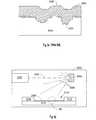
- FIG. 2Ashows a surface 210 of a body region 200 of a transistor.
- the surface 210 in the Figurehas a high degree of smoothness, with a surface variation 220 .
- FIG. 2Bshows the body region 200 during a conventional sputtering deposition process stage.
- particles 230 of the material to be depositedbombard the surface 210 at a high energy.
- particle 235hits the surface 210
- particle 235some particles adhere as shown by particle 235
- other particlescause damage as shown by pit 240 .
- High energy impactscan throw off body region particles 215 to create the pits 240 .
- a resulting layer 250 as deposited by sputteringis shown in FIG. 2C.
- the deposited layer/body region interface 255is shown following a rough contour created by the sputtering damage.
- the surface of the deposited layer 260also shows a rough contour due to the rough interface 255 .
- the deposited layer 250is oxidized to convert the layer 250 to an oxide material.
- Existing oxidation processesdo not, however, repair the surface damage created by existing deposition methods such as sputtering. As described above, surface roughness has a large influence on the electrical properties of the gate dielectric and the resulting transistor.
- any of several materials used to fabricate the transistorsuch as silicon, can react with other materials such as metals or oxygen to form unwanted silicides or oxides.
- materials such as dopantscan also migrate to unwanted areas, changing the desired structure or composition profile. What is needed is a lower temperature process of forming gate dielectrics that prevents migration and the formation of unwanted byproduct materials.
- a method of forming a gate dielectric on a surface such as a transistor body regionis shown where a metal layer is deposited by thermal evaporation on the body region. The metal layer is then oxidized to convert the metal layer to a metal oxide layer. The metal layer is also nitrided to form a metal oxynitride layer. In one embodiment, the metal layer includes zirconium (Zr).
- Zrzirconium
- One embodiment of the inventionuses an electron beam source to evaporate the metal layer onto the body region of the transistor. The oxidation process in one embodiment utilizes a krypton(Kr)/oxygen (O 2 ) mixed plasma process.
- a transistor formed by the novel processexhibits novel features that may only be formed by the novel process.
- Thermal evaporation deposition of a metal layer onto a body region of a transistorpreserves an original smooth surface roughness of the body region in contrast to other prior deposition methods that increase surface roughness.
- the resulting transistor fabricated with the process of this inventionwill exhibit a gate dielectric/body region interface with a surface roughness variation as low as 2.3 angstroms ( ⁇ ).
- the process of thermal evaporation depositionis capable of using highly pure source materials such as zone refined metals.
- the process of thermal evaporationfurther purifies the source material, forming a super high purity metal layer, and a resulting high purity metal oxide layer and high purity metal oxynitride layer.
- FIG. 1shows a common configuration of a transistor.
- FIG. 2Ashows a smooth surface of a body region of a transistor.
- FIG. 2Bshows a deposition process according to the prior art.
- FIG. 2Cshows a deposited film on a body region according to the prior art.
- FIG. 3Ashows a deposition process according to the invention.
- FIG. 3Bshows a magnified view of a deposited film on a body region from FIG. 3A.
- FIG. 4Ashows a deposited film on a body region according to the invention.
- FIG. 4Bshows a partially oxidized film on a body region according to the invention.
- FIG. 4Cshows a completely oxidized film on a body region according to the invention.
- FIG. 4Dshows a partially converted film on a body region according to the invention.
- FIG. 4Eshows a completely converted film on a body region according to the invention.
- FIG. 5shows a perspective view of a personal computer.
- FIG. 6shows a schematic view of a central processing unit.
- FIG. 7shows a schematic view of a DRAM memory device.
- wafer and substrate used in the following descriptioninclude any structure having an exposed surface with which to form the integrated circuit (IC) structure of the invention.
- substrateis understood to include semiconductor wafers.
- substrateis also used to refer to semiconductor structures during processing, and may include other layers that have been fabricated thereupon.
- Both wafer and substrateinclude doped and undoped semiconductors, epitaxial semiconductor layers supported by a base semiconductor or insulator, as well as other semiconductor structures well known to one skilled in the art.
- the term conductoris understood to include semiconductors, and the term insulator or dielectric is defined to include any material that is less electrically conductive than the materials referred to as conductors.
- the term “horizontal” as used in this applicationis defined as a plane parallel to the conventional plane or surface of a wafer or substrate, regardless of the orientation of the wafer or substrate.
- the term “vertical”refers to a direction perpendicular to the horizonal as defined above. Prepositions, such as “on”, “side” (as in “sidewall”), “higher”, “lower”, “over” and “under” are defined with respect to the conventional plane or surface being on the top surface of the wafer or substrate, regardless of the orientation of the wafer or substrate.
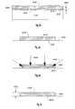
- FIG. 3Ashows an electron beam evaporation technique to deposit a material on a surface such as a body region of a transistor.
- a substrate 310is placed inside a deposition chamber 300 .
- the substrate in this embodimentis masked by a first masking structure 312 and a second masking structure 314 .
- the unmasked region 316includes a body region of a transistor, however one skilled in the art will recognize that other semiconductor device structures may utilize this process.
- an electron beam source 330located within the deposition chamber 300 is an electron beam source 330 , and a target 334 .
- a single electron beam sourceis used and a single target is used. However multiple targets and electron beam sources could be used.
- a single targetis used that includes a single element.
- the single elementincludes a metal.
- more than one elementis included in the target.
- an electron beam evaporation techniqueis used, it will be apparent to one skilled in the art that other thermal evaporation techniques can be used without departing from the scope of the invention.
- the electron beam source 330During the evaporation process, the electron beam source 330 generates an electron beam 332 .
- the electron beamhits the target 334 and heats a portion of the target enough to cause the surface of the target to evaporate.
- the evaporated material 336is then distributed throughout the chamber 300 , and the material 336 deposits on surfaces that it contacts, such as the exposed body region 316 .
- the depositing materialbuilds up to form a layer 320 of material that is chemically the same as the target 334 .
- the evaporation processis performed at a background pressure of approximately 1 ⁇ 10 ⁇ 7 torr.
- the targetis preheated for several minutes before the evaporation process begins.
- One typical evaporation rate for this processincludes a rate of 0.5 to 1.0 nm/second.
- a devicesuch as a quartz crystal microbalance is used to assist monitoring of the deposition process in one embodiment.
- the deposited material layer 320includes a single metal layer.
- the deposited material layer 320includes zirconium (Zr).
- Zrzirconium
- One advantage of the thermal evaporation processis the high purity targets that are available for the process. Targets such as zone refined targets or ultra high vacuum (uhv) melted targets have purity as high as 99.9999%. Additionally, the evaporation process itself further purifies the target materials thus increasing the final purity of the layer 320 beyond even the target purity. The more violent nature of other deposition methods mixes impurities into the deposited layer during deposition. Therefore a uniquely pure layer 320 and further, a uniquely pure layer oxide or other dielectric layer is possible using this novel method.
- the choice of materials for forming a dielectricis based on the properties of the dielectric formed. Considerations included the thermodynamic stability of the dielectric with silicon, the diffusion coefficient of the dielectric at high processing temperatures such as 1000° K, the lattice match of the dielectric with silicon, the dielectric constant of the dielectric, and the conduction band offset of the dielectric.
- the dielectric constantis approximately 25, which is approximately six times the dielectric constant of SiO 2 .
- the deposited material layer 320is substantially amorphous. A lower presence of grain boundaries in the substantially amorphous material layer 320 reduces the leakage current through the final gate dielectric. Although the amorphous form is preferred, the materials chosen for oxidation, such zirconium are also acceptable in crystalline form.
- a thermal evaporation processsuch as the electron beam evaporation technique described above does not cause the surface damage that is inherent in other deposition techniques such as the sputtering technique shown in FIG. 2B. This allows a very thin layer of material to be deposited on a body region of a transistor, while maintaining a smooth interface.
- a thermal evaporation processsuch as the electron beam evaporation technique described above also allows low processing temperatures that inhibit the formation of unwanted byproducts such as silicides and oxides.
- the thermal evaporationis performed with a substrate temperature between approximately 150 and 400° C. In a further embodiment, the thermal evaporation is performed with a substrate temperature between approximately 150 and 200° C.
- FIG. 3Bshows a magnified view of the body region 316 and the deposited layer 320 from FIG. 3A.
- the interface 340is shown with a roughness variation 346 .
- the surface of the deposited layer 348is also shown with a similar surface roughness.
- One possible surface variation 346would be an atomic layer variation.
- atomic smoothnessthe greatest difference in surface features is between a first atomic layer as indicated by layer 342 and a second atomic layer 344 .
- the thermal evaporation deposition technique described abovepreserves atomic smoothness such as is shown in FIG. 3B, however other acceptable levels of surface roughness greater than atomic smoothness will also be preserved by the thermal evaporation technique.
- FIGS. 4A-4Cshow a low temperature oxidation process that is used in one embodiment to convert the deposited layer 320 into an oxide layer.
- a deposited material layer 410is shown in FIG. 4A on a substrate surface 400 .
- the layer 410forms an interface 420 with the substrate surface 400 , and the layer 410 has an outer surface 430 .
- the layer 410 in this embodimentis deposited over a body region of a transistor, however the layer may be deposited on any surface within the scope of the invention.
- the layer 410is in the process of being oxidized.
- the oxidation processincludes a krypton/oxygen mixed plasma oxidation process.
- the mixed plasma processgenerates atomic oxygen or oxygen radicals in contrast to molecular oxygen or O 2 used in conventional thermal oxidation.
- the atomic oxygen in this embodimentis generated by microwave excitation of the krypton and oxygen environment to form a high-density plasma.
- the atomic oxygenis introduced to the layer from all exposed directions as indicated by arrows 440 , creating an oxide portion 450 .
- the atomic oxygencontinues to react with the layer and creates an oxidation interface 422 .
- FIG. 4Cshows the resulting oxide layer 450 which spans a physical thickness 452 from the outer surface 430 to the interface 420 .
- the processing variables for the mixed plasma oxidationinclude a low ion bombardment energy of less than 7 eV, a high plasma density above 10 12 /cm 3 and a low electron temperature below 1.3 eV.
- the substrate temperatureis approximately 400° C.
- a mixed gas of 3% oxygen with the balance being krypton at a pressure of 1 Torris used.
- a microwave power density of 5 W/cm 2is used.
- the oxidation processprovides a growth rate of 1.5 nm/min.
- the low substrate temperature of the mixed plasma oxidation process described aboveallows the deposited layer to be oxidized at a low temperature, which inhibits the formation of unwanted byproducts such as silicides and oxides.
- the low temperaturealso inhibits migration of elements such as dopant species. Low migration preserves designed atomic distribution profiles, thus allowing more advanced device designs and providing higher reliability in existing device designs.
- the mixed plasma oxidation processin one embodiment is performed at approximately 400° C. in contrast to prior thermal oxidation processes that are performed at approximately 1000° C.
- the mixed plasma oxidation processhas also been shown to provide improved thickness variation on silicon (111) surfaces in addition to (100) surfaces.
- FIGS. 4D and 4Eshow a nitridation process that is further performed on the deposited material layer 410 .
- the nitridation processis performed after the oxidation process described above, however one skilled in the art will recognize that nitrogen atoms may also be introduced to the deposited layer 410 prior to an oxidation operation.
- the oxide layer 450is in the process of being nitrided.
- Nitridingis generally defined in this specification as the introduction of nitrogen atoms to an existing microstructure. Introduction of nitrogen to the oxide layer 450 creates an oxynitride structure.
- an oxynitride structureis represented by MO x N y where nitrogen atoms (N) are incorporated into the microstructure of the oxide layer.
- Nnitrogen atoms
- 3-5 atomic percent nitrogenis incorporated into the microstructure of the oxide layer.
- the oxide layer 450is introduced to an ammonia environment (NH 3 ) as a source of nitrogen in the nitriding process.
- NH 3ammonia environment
- annealing process using NH 3is performed at a temperature of approximately 700° C.
- Nitrogenis introduced to the layer from all exposed directions as indicated by arrows 460 , creating an oxynitride portion 470 .
- the nitrogencontinues to diffuse into the layer and creates an interface 424 .
- nitrogen atomsdiffuse through the oxynitride portion 470 and past the interface 424 until the layer is completely converted to an oxynitride layer 470 .
- FIG. 4Eshows the resulting oxynitride layer 470 which spans a physical thickness 454 from the outer surface 430 to the interface 420 .
- the zirconium oxynitride(ZrO x N y ) exhibits a dielectric constant of approximately 25, which allows for a thinner EOT than conventional SiO 2 .
- the novel process used to form the dielectric layeris performed at lower temperatures than the prior art. This inhibits reactions with the silicon substrate or other structures, and inhibits unwanted migration of elements such as dopants.
- zirconium oxide (ZrO 2 )tends to form a polycrystalline phase surface with a high curvature surface.
- the addition of nitrogeninhibits the formation of the crystalline phase. This reduces the surface roughness of the oxynitride layer 470 as compared to zirconium oxide (ZrO 2 ) by approximately a factor of two.
- an amorphous phasein general, is preferred to a crystalline phase due to a lower presence of grain boundaries. Amorphous phases have fewer grain boundaries in the microstructure, which reduces the leakage current through the final gate dielectric.
- a transistor made using the novel gate dielectric process described abovewill possess several novel features.
- a gate dielectriccan be formed with an EOT thinner than 2 nm.
- a thicker gate dielectric that is more uniform, and easier to processcan also be formed with the alternate material dielectric of the present invention, the alternate material gate dielectric possessing an EOT equivalent to the current limits of SiO 2 gate dielectrics.
- the smooth surface of the body regionis preserved during processing, and a resulting transistor will have a smooth interface between the body region and the gate dielectric with a surface roughness as low as 2.3 angstroms ( ⁇ ).
- ⁇angstroms
- Transistors created by the methods described abovemay be implemented into memory devices and information handling devices as shown in FIGS. 5-7 and described below. While specific types of memory devices and computing devices are shown below, it will be recognized by one skilled in the art that several types of memory devices and information handling devices could utilize the invention.
- a personal computeras shown in FIGS. 5 and 6, include a monitor 500 , keyboard input 502 and a central processing unit 504 .
- the processor unittypically includes microprocessor 606 , memory bus circuit 608 having a plurality of memory slots 612 ( a -n), and other peripheral circuitry 610 .
- Peripheral circuitry 610permits various peripheral devices 624 to interface processor-memory bus 620 over input/output (I/O) bus 622 .
- the personal computer shown in FIGS. 5 and 6also includes at least one transistor having a gate dielectric according to the teachings of the present invention.
- Microprocessor 606produces control and address signals to control the exchange of data between memory bus circuit 608 and microprocessor 606 and between memory bus circuit 608 and peripheral circuitry 610 . This exchange of data is accomplished over high speed memory bus 620 and over high speed I/O bus 622 .
- Coupled to memory bus 620are a plurality of memory slots 612 ( a - n ) which receive memory devices well known to those skilled in the art.
- memory slots 612a - n
- SIMMssingle in-line memory modules
- DIMMsdual in-line memory modules
- Page mode operations in a DRAMare defined by the method of accessing a row of a memory cell arrays and randomly accessing different columns of the array. Data stored at the row and column intersection can be read and output while that column is accessed. Page mode DRAMs require access steps which limit the communication speed of memory circuit 608 . A typical communication speed for a DRAM device using page mode is approximately 33 MHZ.
- An alternate type of deviceis the extended data output (EDO) memory which allows data stored at a memory array address to be available as output after the addressed column has been closed. This memory can increase some communication speeds by allowing shorter access signals without reducing the time in which memory output data is available on memory bus 620 .
- EDOextended data output
- Other alternative types of devicesinclude SDRAM, DDR SDRAM, SLDRAM and Direct RDRAM as well as others such as SRAM or Flash memories.
- FIG. 7is a block diagram of an illustrative DRAM device 700 compatible with memory slots 612 ( a - n ).
- the description of DRAM 700has been simplified for purposes of illustrating a DRAM memory device and is not intended to be a complete description of all the features of a DRAM. Those skilled in the art will recognize that a wide variety of memory devices may be used in the implementation of the present invention.
- the example of a DRAM memory device shown in FIG. 7includes at least one transistor having a gate dielectric according to the teachings of the present invention.
- Control, address and data information provided over memory bus 620is further represented by individual inputs to DRAM 700 , as shown in FIG. 7. These individual representations are illustrated by data lines 702 , address lines 704 and various discrete lines directed to control logic 706 .
- DRAM 700includes memory array 710 which in turn comprises rows and columns of addressable memory cells. Each memory cell in a row is coupled to a common wordline. Additionally, each memory cell in a column is coupled to a common bitline. Each cell in memory array 710 includes a storage capacitor and an access transistor as is conventional in the art.
- DRAM 700interfaces with, for example, microprocessor 606 through address lines 704 and data lines 702 .
- DRAM 700may interface with a DRAM controller, a micro-controller, a chip set or other electronic system.
- Microprocessor 606also provides a number of control signals to DRAM 700 , including but not limited to, row and column address strobe signals RAS and CAS, write enable signal WE, an output enable signal OE and other conventional control signals.
- Row address buffer 712 and row decoder 714receive and decode row addresses from row address signals provided on address lines 704 by microprocessor 606 . Each unique row address corresponds to a row of cells in memory array 710 .
- Row decoder 714includes a wordline driver, an address decoder tree, and circuitry which translates a given row address received from row address buffers 712 and selectively activates the appropriate wordline of memory array 710 via the wordline drivers.
- Column address buffer 716 and column decoder 718receive and decode column address signals provided on address lines 704 .
- Column decoder 718also determines when a column is defective and the address of a replacement column.
- Column decoder 718is coupled to sense amplifiers 720 .
- Sense amplifiers 720are coupled to complementary pairs of bitlines of memory array 710 .
- Sense amplifiers 720are coupled to data-in buffer 722 and data-out buffer 724 .
- Data-in buffers 722 and data-out buffers 724are coupled to data lines 702 .
- data lines 702provide data to data-in buffer 722 .
- Sense amplifier 720receives data from data-in buffer 722 and stores the data in memory array 710 as a charge on a capacitor of a cell at an address specified on address lines 704 .
- DRAM 700transfers data to microprocessor 606 from memory array 710 .
- Complementary bitlines for the accessed cellare equilibrated during a precharge operation to a reference voltage provided by an equilibration circuit and a reference voltage supply.
- the charge stored in the accessed cellis then shared with the associated bitlines.
- a sense amplifier of sense amplifiers 720detects and amplifies a difference in voltage between the complementary bitlines.
- the sense amplifierpasses the amplified voltage to data-out buffer 724 .
- Control logic 706is used to control the many available functions of DRAM 700 .
- various control circuits and signals not detailed hereininitiate and synchronize DRAM 700 operation as known to those skilled in the art.
- the description of DRAM 700has been simplified for purposes of illustrating the present invention and is not intended to be a complete description of all the features of a DRAM.
- memory devicesincluding but not limited to, SDRAMs, SLDRAMs, RDRAMs and other DRAMs and SRAMs, VRAMs and EEPROMs, may be used in the implementation of the present invention.
- the DRAM implementation described hereinis illustrative only and not intended to be exclusive or limiting.
- a gate dielectric and method of fabricating a gate dielectricthat produces a more reliable and thinner equivalent oxide thickness.
- Gate dielectrics formed using the methods described hereinare thermodynamically stable such that the gate dielectrics formed will have minimal reactions with a silicon substrate or other structures during any later high temperature processing stages.
- Zirconium oxynitride (ZrO x N y )in particular provides excellent electrical and thermodynamic properties.
- the process shownis performed at lower temperatures than the prior art. This inhibits reactions with the silicon substrate or other structures, and inhibits unwanted migration of elements such as dopants.
- Transistors and higher level ICs or devicesare provided utilizing the novel gate dielectric and process of formation.
- the higher dielectric constant (k) dielectric materials shown in one embodimentare formed with an EOT thinner than 2 nm, e.g. thinner than possible with conventional SiO 2 gate dielectrics.
- a thicker gate dielectric that is more uniform, and easier to processis also provided with at EOT equivalent to the current limits of SiO 2 gate dielectrics.
- a novel process of forming a gate dielectricis provided where the surface smoothness of the body region is preserved during processing, and the resulting transistor has a smooth interface between the body region and the gate dielectric with a surface roughness as low as 2.3 angstroms ( ⁇ ).
- the novel process shownallows the use of highly pure source materials to form the gate dielectric, that are further purified to a unique level during the deposition process. As a result, an ultra-high purity gate dielectric layer is created that further improves the electrical properties of the dielectric layer. Also, the introduction of nitrogen to the dielectric layer promotes an amorphous structure which further reduces the leakage current through the dielectric layer.
Landscapes
- Engineering & Computer Science (AREA)
- Chemical & Material Sciences (AREA)
- Chemical Kinetics & Catalysis (AREA)
- Manufacturing & Machinery (AREA)
- Computer Hardware Design (AREA)
- Microelectronics & Electronic Packaging (AREA)
- Power Engineering (AREA)
- General Physics & Mathematics (AREA)
- Condensed Matter Physics & Semiconductors (AREA)
- Physics & Mathematics (AREA)
- Crystallography & Structural Chemistry (AREA)
- General Chemical & Material Sciences (AREA)
- Materials Engineering (AREA)
- Organic Chemistry (AREA)
- Metallurgy (AREA)
- Mechanical Engineering (AREA)
- Insulated Gate Type Field-Effect Transistor (AREA)
Abstract
Description
- This application is a divisional of U.S. application Ser. No. 10/052,983 filed on Jan. 17, 2002 which is incorporated herein by reference.[0001]
- The invention relates to semiconductor devices and device fabrication. Specifically, the invention relates to gate dielectric layers of transistor devices and their method of fabrication.[0002]
- In the semiconductor device industry, particularly in the fabrication of transistors, there is continuous pressure to reduce the size of devices such as transistors. The ultimate goal is to fabricate increasingly smaller and more reliable integrated circuits (ICs) for use in products such as processor chips, mobile telephones, or memory devices such as DRAMs. The smaller devices are frequently powered by batteries, where there is also pressure to reduce the size of the batteries, and to extend the time between battery charges. This forces the industry to not only design smaller transistors, but to design them to operate reliably with lower power supplies.[0003]
- A common configuration of a transistor is shown in FIG. 1. While the following discussion uses FIG. 1 to illustrate a transistor from the prior art, one skilled in the art will recognize that the present invention could be incorporated into the transistor shown in FIG. 1 to form a novel transistor according to the invention. The[0004]
transistor 100 is fabricated in asubstrate 110 that is typically silicon, but could be fabricated from other semiconductor materials as well. Thetransistor 100 has a first source/drain region 120 and a second source/drain region 130. Abody region 132 is located between the first source/drain region and the second source/drain region, thebody region 132 defining a channel of the transistor with achannel length 134. A gate dielectric, orgate oxide 140 is located on thebody region 132 with agate 150 located over the gate dielectric. Although the gate dielectric can be formed from materials other than oxides, the gate dielectric is typically an oxide, and is commonly referred to as a gate oxide. The gate may be fabricated from polycrystalline silicon (polysilicon) or other conducting materials such as metal may be used. - In fabricating transistors to be smaller in size and reliably operating on lower power supplies, one important design criteria is the gate dielectric[0005]140. A gate dielectric140, when operating in a transistor, has both a physical gate dielectric thickness and an equivalent oxide thickness (EOT). The equivalent oxide thickness quantifies the electrical properties, such as capacitance, of a gate dielectric140 in terms of a representative physical thickness. EOT is defined as the thickness of a theoretical SiO2layer that describes the actual electrical operating characteristics of the gate dielectric140 in the
transistor 100. For example, in traditional SiO2gate oxides, a physical dielectric thickness may be 5.0 nm, but due to undesirable electrical effects such as gate depletion, the EOT may be 6.0 nm. A gate dielectric other than SiO2may also be described electrically in terms of an EOT. In this case, the theoretical dielectric referred to in the EOT number is an equivalent SiO2oxide layer. For example, SiO2has a dielectric constant of approximately 4. An alternate dielectric with a dielectric constant of 20 and a physical thickness of 100 nm would have an EOT of approximately 20 nm=(100*({fraction (4/20)})), which represents a theoretical SiO2gate oxide. - Lower transistor operating voltages and smaller transistors require thinner equivalent oxide thicknesses (EOTs). A problem with the increasing pressure of smaller transistors and lower operating voltages is that gate dielectrics fabricated from SiO[0006]2are at their limit with regards to physical thickness and EOT. Attempts to fabricate SiO2gate dielectrics thinner than today's physical thicknesses show that these gate dielectrics no longer have acceptable electrical properties. As a result, the EOT of a SiO2gate dielectric140 can no longer be reduced by merely reducing the physical gate dielectric thickness.
- Attempts to solve this problem have led to interest in gate dielectrics made from dielectric materials other than SiO[0007]2. Certain alternate dielectrics have a higher dielectric constant (k), which allows the physical thickness of a gate dielectric140 to be the same as existing SiO2limits or thicker, but provides an EOT that is thinner than current SiO2limits.
- A problem that arises in forming an alternate dielectric layer on the body region of a transistor is the process in which the alternate dielectric is formed on the body region. Recent studies show that the surface roughness of the body region has a large effect on the electrical properties of the gate dielectric, and the resulting operating characteristics of the transistor. The leakage current through a physical 1.0 nm gate dielectric increases by a factor of 10 for every 0.1 increase in the root-mean-square (RMS) roughness. In forming an alternate dielectric layer on the body region of a transistor, a thin layer of the alternate material to be oxidized (typically a metal) must first be deposited on the body region. Current processes for depositing a metal or other alternate layer on the body region of a transistor are unacceptable due to their effect on the surface roughness of the body region.[0008]
- FIG. 2A shows a[0009]
surface 210 of abody region 200 of a transistor. Thesurface 210 in the Figure has a high degree of smoothness, with asurface variation 220. FIG. 2B shows thebody region 200 during a conventional sputtering deposition process stage. During sputtering,particles 230 of the material to be deposited bombard thesurface 210 at a high energy. When aparticle 230 hits thesurface 210, some particles adhere as shown byparticle 235, and other particles cause damage as shown bypit 240. High energy impacts can throw offbody region particles 215 to create thepits 240. A resultinglayer 250 as deposited by sputtering is shown in FIG. 2C. The deposited layer/body region interface 255 is shown following a rough contour created by the sputtering damage. The surface of the depositedlayer 260 also shows a rough contour due to therough interface 255. - In a typical process of forming an alternate material gate dielectric, the deposited[0010]
layer 250 is oxidized to convert thelayer 250 to an oxide material. Existing oxidation processes do not, however, repair the surface damage created by existing deposition methods such as sputtering. As described above, surface roughness has a large influence on the electrical properties of the gate dielectric and the resulting transistor. - What is needed is an alternate material gate dielectric that is more reliable at existing EOTs than current gate dielectrics. What is also needed is an alternate material gate dielectric with an EOT thinner than conventional SiO[0011]2. What is also needed is an alternative material gate dielectric with a smooth interface between the gate dielectric and the body region. Because existing methods of deposition are not capable of providing a smooth interface with an alternate material gate dielectric, what is further needed is a method of forming an alternate material gate dielectric that maintains a smooth interface.
- Additionally, at higher process temperatures, any of several materials used to fabricate the transistor, such as silicon, can react with other materials such as metals or oxygen to form unwanted silicides or oxides. At high process temperatures, materials such as dopants can also migrate to unwanted areas, changing the desired structure or composition profile. What is needed is a lower temperature process of forming gate dielectrics that prevents migration and the formation of unwanted byproduct materials.[0012]
- A method of forming a gate dielectric on a surface such as a transistor body region is shown where a metal layer is deposited by thermal evaporation on the body region. The metal layer is then oxidized to convert the metal layer to a metal oxide layer. The metal layer is also nitrided to form a metal oxynitride layer. In one embodiment, the metal layer includes zirconium (Zr). One embodiment of the invention uses an electron beam source to evaporate the metal layer onto the body region of the transistor. The oxidation process in one embodiment utilizes a krypton(Kr)/oxygen (O[0013]2) mixed plasma process.
- In addition to the novel process of forming a gate dielectric layer, a transistor formed by the novel process exhibits novel features that may only be formed by the novel process. Thermal evaporation deposition of a metal layer onto a body region of a transistor preserves an original smooth surface roughness of the body region in contrast to other prior deposition methods that increase surface roughness. The resulting transistor fabricated with the process of this invention will exhibit a gate dielectric/body region interface with a surface roughness variation as low as 2.3 angstroms (Å).[0014]
- The process of thermal evaporation deposition is capable of using highly pure source materials such as zone refined metals. The process of thermal evaporation further purifies the source material, forming a super high purity metal layer, and a resulting high purity metal oxide layer and high purity metal oxynitride layer.[0015]
- These and other embodiments, aspects, advantages, and features of the present invention will be set forth in part in the description which follows, and in part will become apparent to those skilled in the art by reference to the following description of the invention and referenced drawings or by practice of the invention. The aspects, advantages, and features of the invention are realized and attained by means of the instrumentalities, procedures, and combinations particularly pointed out in the appended claims.[0016]
- FIG. 1 shows a common configuration of a transistor.[0017]
- FIG. 2A shows a smooth surface of a body region of a transistor.[0018]
- FIG. 2B shows a deposition process according to the prior art.[0019]
- FIG. 2C shows a deposited film on a body region according to the prior art.[0020]
- FIG. 3A shows a deposition process according to the invention.[0021]
- FIG. 3B shows a magnified view of a deposited film on a body region from FIG. 3A.[0022]
- FIG. 4A shows a deposited film on a body region according to the invention.[0023]
- FIG. 4B shows a partially oxidized film on a body region according to the invention.[0024]
- FIG. 4C shows a completely oxidized film on a body region according to the invention.[0025]
- FIG. 4D shows a partially converted film on a body region according to the invention.[0026]
- FIG. 4E shows a completely converted film on a body region according to the invention.[0027]
- FIG. 5 shows a perspective view of a personal computer.[0028]
- FIG. 6 shows a schematic view of a central processing unit.[0029]
- FIG. 7 shows a schematic view of a DRAM memory device.[0030]
- In the following detailed description of the invention, reference is made to the accompanying drawings which form a part hereof, and in which is shown, by way of illustration, specific embodiments in which the invention may be practiced. In the drawings, like numerals describe substantially similar components throughout the several views. These embodiments are described in sufficient detail to enable those skilled in the art to practice the invention. Other embodiments may be utilized and structural, logical, and electrical changes may be made without departing from the scope of the present invention. The terms wafer and substrate used in the following description include any structure having an exposed surface with which to form the integrated circuit (IC) structure of the invention. The term substrate is understood to include semiconductor wafers. The term substrate is also used to refer to semiconductor structures during processing, and may include other layers that have been fabricated thereupon. Both wafer and substrate include doped and undoped semiconductors, epitaxial semiconductor layers supported by a base semiconductor or insulator, as well as other semiconductor structures well known to one skilled in the art. The term conductor is understood to include semiconductors, and the term insulator or dielectric is defined to include any material that is less electrically conductive than the materials referred to as conductors.[0031]
- The term “horizontal” as used in this application is defined as a plane parallel to the conventional plane or surface of a wafer or substrate, regardless of the orientation of the wafer or substrate. The term “vertical” refers to a direction perpendicular to the horizonal as defined above. Prepositions, such as “on”, “side” (as in “sidewall”), “higher”, “lower”, “over” and “under” are defined with respect to the conventional plane or surface being on the top surface of the wafer or substrate, regardless of the orientation of the wafer or substrate. The following detailed description is, therefore, not to be taken in a limiting sense, and the scope of the present invention is defined only by the appended claims, along with the full scope of equivalents to which such claims are entitled.[0032]
- FIG. 3A shows an electron beam evaporation technique to deposit a material on a surface such as a body region of a transistor. In FIG. 3A, a[0033]
substrate 310 is placed inside adeposition chamber 300. The substrate in this embodiment is masked by afirst masking structure 312 and asecond masking structure 314. In this embodiment, theunmasked region 316 includes a body region of a transistor, however one skilled in the art will recognize that other semiconductor device structures may utilize this process. Also located within thedeposition chamber 300 is anelectron beam source 330, and atarget 334. In one embodiment, a single electron beam source is used and a single target is used. However multiple targets and electron beam sources could be used. In one embodiment, a single target is used that includes a single element. In one embodiment, the single element includes a metal. In alternative embodiments, more than one element is included in the target. Although in one embodiment, an electron beam evaporation technique is used, it will be apparent to one skilled in the art that other thermal evaporation techniques can be used without departing from the scope of the invention. - During the evaporation process, the[0034]
electron beam source 330 generates anelectron beam 332. The electron beam hits thetarget 334 and heats a portion of the target enough to cause the surface of the target to evaporate. The evaporatedmaterial 336 is then distributed throughout thechamber 300, and the material336 deposits on surfaces that it contacts, such as the exposedbody region 316. The depositing material builds up to form alayer 320 of material that is chemically the same as thetarget 334. - In one embodiment, the evaporation process is performed at a background pressure of approximately 1×10[0035]−7torr. In one embodiment the target is preheated for several minutes before the evaporation process begins. One typical evaporation rate for this process includes a rate of 0.5 to 1.0 nm/second. A device such as a quartz crystal microbalance is used to assist monitoring of the deposition process in one embodiment.
- In one embodiment of the invention, the deposited[0036]
material layer 320 includes a single metal layer. In one embodiment of the invention, the depositedmaterial layer 320 includes zirconium (Zr). One advantage of the thermal evaporation process is the high purity targets that are available for the process. Targets such as zone refined targets or ultra high vacuum (uhv) melted targets have purity as high as 99.9999%. Additionally, the evaporation process itself further purifies the target materials thus increasing the final purity of thelayer 320 beyond even the target purity. The more violent nature of other deposition methods mixes impurities into the deposited layer during deposition. Therefore a uniquelypure layer 320 and further, a uniquely pure layer oxide or other dielectric layer is possible using this novel method. - The choice of materials for forming a dielectric is based on the properties of the dielectric formed. Considerations included the thermodynamic stability of the dielectric with silicon, the diffusion coefficient of the dielectric at high processing temperatures such as 1000° K, the lattice match of the dielectric with silicon, the dielectric constant of the dielectric, and the conduction band offset of the dielectric. In one embodiment, the dielectric constant is approximately 25, which is approximately six times the dielectric constant of SiO[0037]2. In one embodiment, the deposited
material layer 320 is substantially amorphous. A lower presence of grain boundaries in the substantiallyamorphous material layer 320 reduces the leakage current through the final gate dielectric. Although the amorphous form is preferred, the materials chosen for oxidation, such zirconium are also acceptable in crystalline form. - A thermal evaporation process such as the electron beam evaporation technique described above does not cause the surface damage that is inherent in other deposition techniques such as the sputtering technique shown in FIG. 2B. This allows a very thin layer of material to be deposited on a body region of a transistor, while maintaining a smooth interface. A thermal evaporation process such as the electron beam evaporation technique described above also allows low processing temperatures that inhibit the formation of unwanted byproducts such as silicides and oxides. In one embodiment, the thermal evaporation is performed with a substrate temperature between approximately 150 and 400° C. In a further embodiment, the thermal evaporation is performed with a substrate temperature between approximately 150 and 200° C.[0038]
- FIG. 3B shows a magnified view of the[0039]
body region 316 and the depositedlayer 320 from FIG. 3A. Theinterface 340 is shown with aroughness variation 346. The surface of the depositedlayer 348 is also shown with a similar surface roughness. Onepossible surface variation 346 would be an atomic layer variation. In atomic smoothness, the greatest difference in surface features is between a first atomic layer as indicated bylayer 342 and a secondatomic layer 344. The thermal evaporation deposition technique described above preserves atomic smoothness such as is shown in FIG. 3B, however other acceptable levels of surface roughness greater than atomic smoothness will also be preserved by the thermal evaporation technique. - FIGS. 4A-4C show a low temperature oxidation process that is used in one embodiment to convert the deposited[0040]
layer 320 into an oxide layer. A depositedmaterial layer 410 is shown in FIG. 4A on asubstrate surface 400. Thelayer 410 forms aninterface 420 with thesubstrate surface 400, and thelayer 410 has anouter surface 430. Thelayer 410 in this embodiment is deposited over a body region of a transistor, however the layer may be deposited on any surface within the scope of the invention. - In FIG. 4B, the[0041]
layer 410 is in the process of being oxidized. In one embodiment, the oxidation process includes a krypton/oxygen mixed plasma oxidation process. The mixed plasma process generates atomic oxygen or oxygen radicals in contrast to molecular oxygen or O2used in conventional thermal oxidation. The atomic oxygen in this embodiment is generated by microwave excitation of the krypton and oxygen environment to form a high-density plasma. The atomic oxygen is introduced to the layer from all exposed directions as indicated byarrows 440, creating anoxide portion 450. The atomic oxygen continues to react with the layer and creates anoxidation interface 422. As the reaction progresses, atomic oxygen diffuses through theoxide portion 450 and reacts at theoxidation interface 422 until the layer is completely converted to an oxide of the deposited material layer. FIG. 4C shows the resultingoxide layer 450 which spans aphysical thickness 452 from theouter surface 430 to theinterface 420. - In one embodiment, the processing variables for the mixed plasma oxidation include a low ion bombardment energy of less than 7 eV, a high plasma density above 10[0042]12/cm3and a low electron temperature below 1.3 eV. In one embodiment, the substrate temperature is approximately 400° C. In one embodiment, a mixed gas of 3% oxygen with the balance being krypton at a pressure of 1 Torr is used. In one embodiment, a microwave power density of 5 W/cm2is used. In one embodiment, the oxidation process provides a growth rate of 1.5 nm/min.
- The low substrate temperature of the mixed plasma oxidation process described above allows the deposited layer to be oxidized at a low temperature, which inhibits the formation of unwanted byproducts such as silicides and oxides. The low temperature also inhibits migration of elements such as dopant species. Low migration preserves designed atomic distribution profiles, thus allowing more advanced device designs and providing higher reliability in existing device designs. The mixed plasma oxidation process in one embodiment is performed at approximately 400° C. in contrast to prior thermal oxidation processes that are performed at approximately 1000° C. The mixed plasma oxidation process has also been shown to provide improved thickness variation on silicon (111) surfaces in addition to (100) surfaces. Although the low temperature mixed plasma process above describes the oxidation of alternate material oxides, one skilled in the art will recognize that the process can also be used to form SiO[0043]2oxide structures.
- FIGS. 4D and 4E show a nitridation process that is further performed on the deposited[0044]
material layer 410. In one embodiment, the nitridation process is performed after the oxidation process described above, however one skilled in the art will recognize that nitrogen atoms may also be introduced to the depositedlayer 410 prior to an oxidation operation. - In FIG. 4D, the[0045]
oxide layer 450 is in the process of being nitrided. Nitriding is generally defined in this specification as the introduction of nitrogen atoms to an existing microstructure. Introduction of nitrogen to theoxide layer 450 creates an oxynitride structure. In one embodiment, an oxynitride structure is represented by MOxNywhere nitrogen atoms (N) are incorporated into the microstructure of the oxide layer. In one embodiment, 3-5 atomic percent nitrogen is incorporated into the microstructure of the oxide layer. - In one embodiment the[0046]
oxide layer 450 is introduced to an ammonia environment (NH3) as a source of nitrogen in the nitriding process. In one embodiment, and annealing process using NH3is performed at a temperature of approximately 700° C. Nitrogen is introduced to the layer from all exposed directions as indicated byarrows 460, creating anoxynitride portion 470. The nitrogen continues to diffuse into the layer and creates aninterface 424. As the introduction of nitrogen progresses, nitrogen atoms diffuse through theoxynitride portion 470 and past theinterface 424 until the layer is completely converted to anoxynitride layer 470. FIG. 4E shows the resultingoxynitride layer 470 which spans aphysical thickness 454 from theouter surface 430 to theinterface 420. - The zirconium oxynitride (ZrO[0047]xNy) exhibits a dielectric constant of approximately 25, which allows for a thinner EOT than conventional SiO2. In addition to the stable thermodynamic properties inherent in the dielectrics chosen, the novel process used to form the dielectric layer is performed at lower temperatures than the prior art. This inhibits reactions with the silicon substrate or other structures, and inhibits unwanted migration of elements such as dopants.
- The addition of nitrogen atoms to the microstructure of the[0048]
oxynitride layer 470 - promotes a uniform amorphous phase. In contrast, zirconium oxide (ZrO[0049]2) tends to form a polycrystalline phase surface with a high curvature surface. The addition of nitrogen inhibits the formation of the crystalline phase. This reduces the surface roughness of the
oxynitride layer 470 as compared to zirconium oxide (ZrO2) by approximately a factor of two. Also, as discussed above, an amorphous phase, in general, is preferred to a crystalline phase due to a lower presence of grain boundaries. Amorphous phases have fewer grain boundaries in the microstructure, which reduces the leakage current through the final gate dielectric. - A transistor made using the novel gate dielectric process described above will possess several novel features. By creating a dielectric material with a higher dielectric constant (k) and controlling surface roughness during formation, a gate dielectric can be formed with an EOT thinner than 2 nm. A thicker gate dielectric that is more uniform, and easier to process can also be formed with the alternate material dielectric of the present invention, the alternate material gate dielectric possessing an EOT equivalent to the current limits of SiO[0050]2gate dielectrics. The smooth surface of the body region is preserved during processing, and a resulting transistor will have a smooth interface between the body region and the gate dielectric with a surface roughness as low as 2.3 angstroms (Å). The introduction of nitrogen to the dielectric layer promotes an amorphous structure which further reduces the leakage current through the dielectric layer.
- Transistors created by the methods described above may be implemented into memory devices and information handling devices as shown in FIGS. 5-7 and described below. While specific types of memory devices and computing devices are shown below, it will be recognized by one skilled in the art that several types of memory devices and information handling devices could utilize the invention.[0051]
- A personal computer, as shown in FIGS. 5 and 6, include a[0052]
monitor 500,keyboard input 502 and acentral processing unit 504. The processor unit typically includesmicroprocessor 606,memory bus circuit 608 having a plurality of memory slots612(a-n), and otherperipheral circuitry 610.Peripheral circuitry 610 permits variousperipheral devices 624 to interface processor-memory bus 620 over input/output (I/O)bus 622. The personal computer shown in FIGS. 5 and 6 also includes at least one transistor having a gate dielectric according to the teachings of the present invention. - [0053]
Microprocessor 606 produces control and address signals to control the exchange of data betweenmemory bus circuit 608 andmicroprocessor 606 and betweenmemory bus circuit 608 andperipheral circuitry 610. This exchange of data is accomplished over highspeed memory bus 620 and over high speed I/O bus 622. - Coupled to[0054]
memory bus 620 are a plurality of memory slots612(a-n) which receive memory devices well known to those skilled in the art. For example, single in-line memory modules (SIMMs) and dual in-line memory modules (DIMMs) may be used in the implementation of the present invention. - These memory devices can be produced in a variety of designs which provide different methods of reading from and writing to the dynamic memory cells of[0055]
memory slots 612. One such method is the page mode operation. Page mode operations in a DRAM are defined by the method of accessing a row of a memory cell arrays and randomly accessing different columns of the array. Data stored at the row and column intersection can be read and output while that column is accessed. Page mode DRAMs require access steps which limit the communication speed ofmemory circuit 608. A typical communication speed for a DRAM device using page mode is approximately 33 MHZ. - An alternate type of device is the extended data output (EDO) memory which allows data stored at a memory array address to be available as output after the addressed column has been closed. This memory can increase some communication speeds by allowing shorter access signals without reducing the time in which memory output data is available on[0056]
memory bus 620. Other alternative types of devices include SDRAM, DDR SDRAM, SLDRAM and Direct RDRAM as well as others such as SRAM or Flash memories. - FIG. 7 is a block diagram of an[0057]
illustrative DRAM device 700 compatible with memory slots612(a-n). The description ofDRAM 700 has been simplified for purposes of illustrating a DRAM memory device and is not intended to be a complete description of all the features of a DRAM. Those skilled in the art will recognize that a wide variety of memory devices may be used in the implementation of the present invention. The example of a DRAM memory device shown in FIG. 7 includes at least one transistor having a gate dielectric according to the teachings of the present invention. - Control, address and data information provided over[0058]
memory bus 620 is further represented by individual inputs toDRAM 700, as shown in FIG. 7. These individual representations are illustrated bydata lines 702,address lines 704 and various discrete lines directed to controllogic 706. - As is well known in the art,[0059]
DRAM 700 includesmemory array 710 which in turn comprises rows and columns of addressable memory cells. Each memory cell in a row is coupled to a common wordline. Additionally, each memory cell in a column is coupled to a common bitline. Each cell inmemory array 710 includes a storage capacitor and an access transistor as is conventional in the art. - [0060]
DRAM 700 interfaces with, for example,microprocessor 606 throughaddress lines 704 anddata lines 702. Alternatively,DRAM 700 may interface with a DRAM controller, a micro-controller, a chip set or other electronic system.Microprocessor 606 also provides a number of control signals toDRAM 700, including but not limited to, row and column address strobe signals RAS and CAS, write enable signal WE, an output enable signal OE and other conventional control signals. - [0061]
Row address buffer 712 androw decoder 714 receive and decode row addresses from row address signals provided onaddress lines 704 bymicroprocessor 606. Each unique row address corresponds to a row of cells inmemory array 710.Row decoder 714 includes a wordline driver, an address decoder tree, and circuitry which translates a given row address received from row address buffers712 and selectively activates the appropriate wordline ofmemory array 710 via the wordline drivers. - [0062]
Column address buffer 716 andcolumn decoder 718 receive and decode column address signals provided onaddress lines 704.Column decoder 718 also determines when a column is defective and the address of a replacement column.Column decoder 718 is coupled to senseamplifiers 720.Sense amplifiers 720 are coupled to complementary pairs of bitlines ofmemory array 710. - [0063]
Sense amplifiers 720 are coupled to data-inbuffer 722 and data-outbuffer 724. Data-inbuffers 722 and data-outbuffers 724 are coupled todata lines 702. During a write operation,data lines 702 provide data to data-inbuffer 722.Sense amplifier 720 receives data from data-inbuffer 722 and stores the data inmemory array 710 as a charge on a capacitor of a cell at an address specified onaddress lines 704. - During a read operation,[0064]
DRAM 700 transfers data tomicroprocessor 606 frommemory array 710. Complementary bitlines for the accessed cell are equilibrated during a precharge operation to a reference voltage provided by an equilibration circuit and a reference voltage supply. The charge stored in the accessed cell is then shared with the associated bitlines. A sense amplifier ofsense amplifiers 720 detects and amplifies a difference in voltage between the complementary bitlines. The sense amplifier passes the amplified voltage to data-outbuffer 724. - [0065]
Control logic 706 is used to control the many available functions ofDRAM 700. In addition, various control circuits and signals not detailed herein initiate and synchronizeDRAM 700 operation as known to those skilled in the art. As stated above, the description ofDRAM 700 has been simplified for purposes of illustrating the present invention and is not intended to be a complete description of all the features of a DRAM. Those skilled in the art will recognize that a wide variety of memory devices, including but not limited to, SDRAMs, SLDRAMs, RDRAMs and other DRAMs and SRAMs, VRAMs and EEPROMs, may be used in the implementation of the present invention. The DRAM implementation described herein is illustrative only and not intended to be exclusive or limiting. - Thus a gate dielectric and method of fabricating a gate dielectric is provided that produces a more reliable and thinner equivalent oxide thickness. Gate dielectrics formed using the methods described herein are thermodynamically stable such that the gate dielectrics formed will have minimal reactions with a silicon substrate or other structures during any later high temperature processing stages. Zirconium oxynitride (ZrO[0066]xNy) in particular provides excellent electrical and thermodynamic properties. In addition to the stable thermodynamic properties inherent in the gate dielectric of the invention, the process shown is performed at lower temperatures than the prior art. This inhibits reactions with the silicon substrate or other structures, and inhibits unwanted migration of elements such as dopants.
- Transistors and higher level ICs or devices are provided utilizing the novel gate dielectric and process of formation. The higher dielectric constant (k) dielectric materials shown in one embodiment are formed with an EOT thinner than 2 nm, e.g. thinner than possible with conventional SiO[0067]2gate dielectrics. A thicker gate dielectric that is more uniform, and easier to process is also provided with at EOT equivalent to the current limits of SiO2gate dielectrics.
- A novel process of forming a gate dielectric is provided where the surface smoothness of the body region is preserved during processing, and the resulting transistor has a smooth interface between the body region and the gate dielectric with a surface roughness as low as 2.3 angstroms (Å). This solves the prior art problem of poor electrical properties such as high leakage current, created by unacceptable surface roughness. The novel process shown allows the use of highly pure source materials to form the gate dielectric, that are further purified to a unique level during the deposition process. As a result, an ultra-high purity gate dielectric layer is created that further improves the electrical properties of the dielectric layer. Also, the introduction of nitrogen to the dielectric layer promotes an amorphous structure which further reduces the leakage current through the dielectric layer.[0068]
- Although specific embodiments have been illustrated and described herein, it will be appreciated by those of ordinary skill in the art that any arrangement which is calculated to achieve the same purpose may be substituted for the specific embodiment shown. This application is intended to cover any adaptations or variations of the present invention. It is to be understood that the above description is intended to be illustrative, and not restrictive. Combinations of the above embodiments, and other embodiments will be apparent to those of skill in the art upon reviewing the above description. The scope of the invention includes any other applications in which the above structures and fabrication methods are used. The scope of the invention should be determined with reference to the appended claims, along with the full scope of equivalents to which such claims are entitled.[0069]
Claims (24)
Priority Applications (1)
| Application Number | Priority Date | Filing Date | Title |
|---|---|---|---|
| US10/863,953US7205620B2 (en) | 2002-01-17 | 2004-06-09 | Highly reliable amorphous high-k gate dielectric ZrOxNy |
Applications Claiming Priority (2)
| Application Number | Priority Date | Filing Date | Title |
|---|---|---|---|
| US10/052,983US6767795B2 (en) | 2002-01-17 | 2002-01-17 | Highly reliable amorphous high-k gate dielectric ZrOXNY |
| US10/863,953US7205620B2 (en) | 2002-01-17 | 2004-06-09 | Highly reliable amorphous high-k gate dielectric ZrOxNy |
Related Parent Applications (1)
| Application Number | Title | Priority Date | Filing Date |
|---|---|---|---|
| US10/052,983DivisionUS6767795B2 (en) | 2002-01-17 | 2002-01-17 | Highly reliable amorphous high-k gate dielectric ZrOXNY |
Publications (2)
| Publication Number | Publication Date |
|---|---|
| US20040222476A1true US20040222476A1 (en) | 2004-11-11 |
| US7205620B2 US7205620B2 (en) | 2007-04-17 |
Family
ID=21981153
Family Applications (2)
| Application Number | Title | Priority Date | Filing Date |
|---|---|---|---|
| US10/052,983Expired - LifetimeUS6767795B2 (en) | 2002-01-17 | 2002-01-17 | Highly reliable amorphous high-k gate dielectric ZrOXNY |
| US10/863,953Expired - LifetimeUS7205620B2 (en) | 2002-01-17 | 2004-06-09 | Highly reliable amorphous high-k gate dielectric ZrOxNy |
Family Applications Before (1)
| Application Number | Title | Priority Date | Filing Date |
|---|---|---|---|
| US10/052,983Expired - LifetimeUS6767795B2 (en) | 2002-01-17 | 2002-01-17 | Highly reliable amorphous high-k gate dielectric ZrOXNY |
Country Status (1)
| Country | Link |
|---|---|
| US (2) | US6767795B2 (en) |
Cited By (47)
| Publication number | Priority date | Publication date | Assignee | Title |
|---|---|---|---|---|
| US20040183108A1 (en)* | 2001-12-20 | 2004-09-23 | Micron Technology, Inc. | Low-temperature grown high-quality ultra-thin praseodymium gate dielectrics |
| US7081421B2 (en) | 2004-08-26 | 2006-07-25 | Micron Technology, Inc. | Lanthanide oxide dielectric layer |
| US7084078B2 (en) | 2002-08-29 | 2006-08-01 | Micron Technology, Inc. | Atomic layer deposited lanthanide doped TiOx dielectric films |
| US20060183272A1 (en)* | 2005-02-15 | 2006-08-17 | Micron Technology, Inc. | Atomic layer deposition of Zr3N4/ZrO2 films as gate dielectrics |
| US7129553B2 (en) | 2003-06-24 | 2006-10-31 | Micron Technology, Inc. | Lanthanide oxide/hafnium oxide dielectrics |
| US20060244100A1 (en)* | 2005-04-28 | 2006-11-02 | Micron Technology, Inc. | Atomic layer deposited zirconium silicon oxide films |
| US7135369B2 (en) | 2003-03-31 | 2006-11-14 | Micron Technology, Inc. | Atomic layer deposited ZrAlxOy dielectric layers including Zr4AlO9 |
| US7160577B2 (en) | 2002-05-02 | 2007-01-09 | Micron Technology, Inc. | Methods for atomic-layer deposition of aluminum oxides in integrated circuits |
| US7183186B2 (en) | 2003-04-22 | 2007-02-27 | Micro Technology, Inc. | Atomic layer deposited ZrTiO4 films |
| US7192892B2 (en) | 2003-03-04 | 2007-03-20 | Micron Technology, Inc. | Atomic layer deposited dielectric layers |
| US7192824B2 (en) | 2003-06-24 | 2007-03-20 | Micron Technology, Inc. | Lanthanide oxide / hafnium oxide dielectric layers |
| US7205218B2 (en) | 2002-06-05 | 2007-04-17 | Micron Technology, Inc. | Method including forming gate dielectrics having multiple lanthanide oxide layers |
| US7235501B2 (en) | 2004-12-13 | 2007-06-26 | Micron Technology, Inc. | Lanthanum hafnium oxide dielectrics |
| US7235854B2 (en) | 2002-08-15 | 2007-06-26 | Micron Technology, Inc. | Lanthanide doped TiOx dielectric films |
| US7259434B2 (en) | 2001-08-30 | 2007-08-21 | Micron Technology, Inc. | Highly reliable amorphous high-k gate oxide ZrO2 |
| US7374964B2 (en) | 2005-02-10 | 2008-05-20 | Micron Technology, Inc. | Atomic layer deposition of CeO2/Al2O3 films as gate dielectrics |
| US7393736B2 (en) | 2005-08-29 | 2008-07-01 | Micron Technology, Inc. | Atomic layer deposition of Zrx Hfy Sn1-x-y O2 films as high k gate dielectrics |
| US7402876B2 (en) | 2002-12-04 | 2008-07-22 | Micron Technology, Inc. | Zr— Sn—Ti—O films |
| US7410910B2 (en) | 2005-08-31 | 2008-08-12 | Micron Technology, Inc. | Lanthanum aluminum oxynitride dielectric films |
| US7410668B2 (en) | 2001-03-01 | 2008-08-12 | Micron Technology, Inc. | Methods, systems, and apparatus for uniform chemical-vapor depositions |
| US7429515B2 (en) | 2001-12-20 | 2008-09-30 | Micron Technology, Inc. | Low-temperature grown high quality ultra-thin CoTiO3 gate dielectrics |
| US7446368B2 (en) | 2001-08-30 | 2008-11-04 | Micron Technology, Inc. | Deposition of metal oxide and/or low asymmetrical tunnel barrier interpoly insulators |
| US7494939B2 (en) | 2004-08-31 | 2009-02-24 | Micron Technology, Inc. | Methods for forming a lanthanum-metal oxide dielectric layer |
| US7498247B2 (en) | 2005-02-23 | 2009-03-03 | Micron Technology, Inc. | Atomic layer deposition of Hf3N4/HfO2 films as gate dielectrics |
| US7508648B2 (en) | 2005-02-08 | 2009-03-24 | Micron Technology, Inc. | Atomic layer deposition of Dy doped HfO2 films as gate dielectrics |
| US7510983B2 (en) | 2005-06-14 | 2009-03-31 | Micron Technology, Inc. | Iridium/zirconium oxide structure |
| US7544596B2 (en) | 2005-08-30 | 2009-06-09 | Micron Technology, Inc. | Atomic layer deposition of GdScO3 films as gate dielectrics |
| US7554161B2 (en) | 2002-06-05 | 2009-06-30 | Micron Technology, Inc. | HfAlO3 films for gate dielectrics |
| US7560395B2 (en) | 2005-01-05 | 2009-07-14 | Micron Technology, Inc. | Atomic layer deposited hafnium tantalum oxide dielectrics |
| US7560793B2 (en) | 2002-05-02 | 2009-07-14 | Micron Technology, Inc. | Atomic layer deposition and conversion |
| US7572695B2 (en) | 2005-05-27 | 2009-08-11 | Micron Technology, Inc. | Hafnium titanium oxide films |
| US7582161B2 (en) | 2006-04-07 | 2009-09-01 | Micron Technology, Inc. | Atomic layer deposited titanium-doped indium oxide films |
| US7582549B2 (en) | 2006-08-25 | 2009-09-01 | Micron Technology, Inc. | Atomic layer deposited barium strontium titanium oxide films |
| US7588988B2 (en) | 2004-08-31 | 2009-09-15 | Micron Technology, Inc. | Method of forming apparatus having oxide films formed using atomic layer deposition |
| US7601649B2 (en) | 2004-08-02 | 2009-10-13 | Micron Technology, Inc. | Zirconium-doped tantalum oxide films |
| US7605030B2 (en) | 2006-08-31 | 2009-10-20 | Micron Technology, Inc. | Hafnium tantalum oxynitride high-k dielectric and metal gates |
| US7611959B2 (en) | 2002-12-04 | 2009-11-03 | Micron Technology, Inc. | Zr-Sn-Ti-O films |
| US7662729B2 (en) | 2005-04-28 | 2010-02-16 | Micron Technology, Inc. | Atomic layer deposition of a ruthenium layer to a lanthanide oxide dielectric layer |
| US7687409B2 (en) | 2005-03-29 | 2010-03-30 | Micron Technology, Inc. | Atomic layer deposited titanium silicon oxide films |
| US7709402B2 (en) | 2006-02-16 | 2010-05-04 | Micron Technology, Inc. | Conductive layers for hafnium silicon oxynitride films |
| US7728626B2 (en) | 2002-07-08 | 2010-06-01 | Micron Technology, Inc. | Memory utilizing oxide nanolaminates |
| US7972974B2 (en) | 2006-01-10 | 2011-07-05 | Micron Technology, Inc. | Gallium lanthanide oxide films |
| US8071476B2 (en) | 2005-08-31 | 2011-12-06 | Micron Technology, Inc. | Cobalt titanium oxide dielectric films |
| US8125038B2 (en) | 2002-07-30 | 2012-02-28 | Micron Technology, Inc. | Nanolaminates of hafnium oxide and zirconium oxide |
| US8501563B2 (en) | 2005-07-20 | 2013-08-06 | Micron Technology, Inc. | Devices with nanocrystals and methods of formation |
| CN104599947A (en)* | 2014-12-24 | 2015-05-06 | 上海交通大学 | Zirconia insulation film and preparation method thereof |
| WO2017053481A1 (en)* | 2015-09-21 | 2017-03-30 | Rutgers, The State University Of New Jersey | Magnesium zinc oxide nanostructure modified biosensor and monitoring of response of cell population to an agent using the same |
Families Citing this family (34)
| Publication number | Priority date | Publication date | Assignee | Title |
|---|---|---|---|---|
| US7554829B2 (en) | 1999-07-30 | 2009-06-30 | Micron Technology, Inc. | Transmission lines for CMOS integrated circuits |
| US7068544B2 (en)* | 2001-08-30 | 2006-06-27 | Micron Technology, Inc. | Flash memory with low tunnel barrier interpoly insulators |
| JP4171250B2 (en)* | 2002-06-19 | 2008-10-22 | 東京エレクトロン株式会社 | Manufacturing method of semiconductor device |
| US6884739B2 (en) | 2002-08-15 | 2005-04-26 | Micron Technology Inc. | Lanthanide doped TiOx dielectric films by plasma oxidation |
| US7199023B2 (en)* | 2002-08-28 | 2007-04-03 | Micron Technology, Inc. | Atomic layer deposited HfSiON dielectric films wherein each precursor is independendently pulsed |
| US7037863B2 (en)* | 2002-09-10 | 2006-05-02 | Samsung Electronics Co., Ltd. | Post thermal treatment methods of forming high dielectric layers over interfacial layers in integrated circuit devices |
| US7071117B2 (en)* | 2004-02-27 | 2006-07-04 | Micron Technology, Inc. | Semiconductor devices and methods for depositing a dielectric film |
| US20050233477A1 (en)* | 2004-03-05 | 2005-10-20 | Tokyo Electron Limited | Substrate processing apparatus, substrate processing method, and program for implementing the method |
| KR100728962B1 (en)* | 2004-11-08 | 2007-06-15 | 주식회사 하이닉스반도체 | Capacitor of semiconductor device with zrconium oxide and method of manufacturing the same |
| US20060151822A1 (en)* | 2005-01-07 | 2006-07-13 | Shrinivas Govindarajan | DRAM with high K dielectric storage capacitor and method of making the same |
| US7316962B2 (en)* | 2005-01-07 | 2008-01-08 | Infineon Technologies Ag | High dielectric constant materials |
| US20060151845A1 (en)* | 2005-01-07 | 2006-07-13 | Shrinivas Govindarajan | Method to control interfacial properties for capacitors using a metal flash layer |
| US7365027B2 (en) | 2005-03-29 | 2008-04-29 | Micron Technology, Inc. | ALD of amorphous lanthanide doped TiOx films |
| US7195999B2 (en)* | 2005-07-07 | 2007-03-27 | Micron Technology, Inc. | Metal-substituted transistor gates |
| US7214994B2 (en) | 2005-08-31 | 2007-05-08 | Micron Technology, Inc. | Self aligned metal gates on high-k dielectrics |
| US8471254B2 (en)* | 2005-12-27 | 2013-06-25 | Hana Microdisplay Technologies, Inc. | Liquid crystal cells with uniform cell gap and methods of manufacture |
| US7749879B2 (en)* | 2006-08-03 | 2010-07-06 | Micron Technology, Inc. | ALD of silicon films on germanium |
| US7727908B2 (en) | 2006-08-03 | 2010-06-01 | Micron Technology, Inc. | Deposition of ZrA1ON films |
| US7985995B2 (en) | 2006-08-03 | 2011-07-26 | Micron Technology, Inc. | Zr-substituted BaTiO3 films |
| US7759747B2 (en) | 2006-08-31 | 2010-07-20 | Micron Technology, Inc. | Tantalum aluminum oxynitride high-κ dielectric |
| US7563730B2 (en) | 2006-08-31 | 2009-07-21 | Micron Technology, Inc. | Hafnium lanthanide oxynitride films |
| US7432548B2 (en) | 2006-08-31 | 2008-10-07 | Micron Technology, Inc. | Silicon lanthanide oxynitride films |
| US7544604B2 (en) | 2006-08-31 | 2009-06-09 | Micron Technology, Inc. | Tantalum lanthanide oxynitride films |
| US7776765B2 (en) | 2006-08-31 | 2010-08-17 | Micron Technology, Inc. | Tantalum silicon oxynitride high-k dielectrics and metal gates |
| US20080087890A1 (en)* | 2006-10-16 | 2008-04-17 | Micron Technology, Inc. | Methods to form dielectric structures in semiconductor devices and resulting devices |
| US7498230B2 (en)* | 2007-02-13 | 2009-03-03 | Micron Technology, Inc. | Magnesium-doped zinc oxide structures and methods |
| US8367506B2 (en) | 2007-06-04 | 2013-02-05 | Micron Technology, Inc. | High-k dielectrics with gold nano-particles |
| US8004060B2 (en)* | 2007-11-29 | 2011-08-23 | International Business Machines Corporation | Metal gate compatible electrical antifuse |
| US7728392B2 (en)* | 2008-01-03 | 2010-06-01 | International Business Machines Corporation | SRAM device structure including same band gap transistors having gate stacks with high-K dielectrics and same work function |
| US7943457B2 (en)* | 2009-04-14 | 2011-05-17 | International Business Machines Corporation | Dual metal and dual dielectric integration for metal high-k FETs |
| US8525339B2 (en) | 2011-07-27 | 2013-09-03 | International Business Machines Corporation | Hybrid copper interconnect structure and method of fabricating same |
| KR20140032716A (en) | 2012-09-07 | 2014-03-17 | 삼성전자주식회사 | Semiconductor device and method for fabricating thereof |
| CN104022039B (en)* | 2013-03-01 | 2017-04-05 | 中芯国际集成电路制造(上海)有限公司 | A kind of manufacture method of semiconductor devices |
| US9053926B2 (en) | 2013-03-18 | 2015-06-09 | International Business Machines Corporation | Cyclical physical vapor deposition of dielectric layers |
Citations (88)
| Publication number | Priority date | Publication date | Assignee | Title |
|---|---|---|---|---|
| US3381114A (en)* | 1963-12-28 | 1968-04-30 | Nippon Electric Co | Device for manufacturing epitaxial crystals |
| US4215156A (en)* | 1977-08-26 | 1980-07-29 | International Business Machines Corporation | Method for fabricating tantalum semiconductor contacts |
| US4333808A (en)* | 1979-10-30 | 1982-06-08 | International Business Machines Corporation | Method for manufacture of ultra-thin film capacitor |
| US4394673A (en)* | 1980-09-29 | 1983-07-19 | International Business Machines Corporation | Rare earth silicide Schottky barriers |
| US4399424A (en)* | 1980-10-07 | 1983-08-16 | Itt Industries, Inc. | Gas sensor |
| US4590042A (en)* | 1984-12-24 | 1986-05-20 | Tegal Corporation | Plasma reactor having slotted manifold |
| US4647947A (en)* | 1982-03-15 | 1987-03-03 | Tokyo Shibaura Denki Kabushiki Kaisha | Optical protuberant bubble recording medium |
| US4725877A (en)* | 1986-04-11 | 1988-02-16 | American Telephone And Telegraph Company, At&T Bell Laboratories | Metallized semiconductor device including an interface layer |
| US4767641A (en)* | 1986-03-04 | 1988-08-30 | Leybold-Heraeus Gmbh | Plasma treatment apparatus |
| US4920071A (en)* | 1985-03-15 | 1990-04-24 | Fairchild Camera And Instrument Corporation | High temperature interconnect system for an integrated circuit |
| US4993358A (en)* | 1989-07-28 | 1991-02-19 | Watkins-Johnson Company | Chemical vapor deposition reactor and method of operation |
| US5006192A (en)* | 1988-06-28 | 1991-04-09 | Mitsubishi Denki Kabushiki Kaisha | Apparatus for producing semiconductor devices |
| US5080928A (en)* | 1990-10-05 | 1992-01-14 | Gte Laboratories Incorporated | Method for making moisture insensitive zinc sulfide based luminescent materials |
| US5198029A (en)* | 1989-08-01 | 1993-03-30 | Gte Products Corporation | Apparatus for coating small solids |
| US5302461A (en)* | 1992-06-05 | 1994-04-12 | Hewlett-Packard Company | Dielectric films for use in magnetoresistive transducers |
| US5595606A (en)* | 1995-04-20 | 1997-01-21 | Tokyo Electron Limited | Shower head and film forming apparatus using the same |
| US5621681A (en)* | 1995-03-22 | 1997-04-15 | Samsung Electronics Co., Ltd. | Device and manufacturing method for a ferroelectric memory |
| US5625233A (en)* | 1995-01-13 | 1997-04-29 | Ibm Corporation | Thin film multi-layer oxygen diffusion barrier consisting of refractory metal, refractory metal aluminide, and aluminum oxide |
| US5735960A (en)* | 1996-04-02 | 1998-04-07 | Micron Technology, Inc. | Apparatus and method to increase gas residence time in a reactor |
| US5789030A (en)* | 1996-03-18 | 1998-08-04 | Micron Technology, Inc. | Method for depositing doped amorphous or polycrystalline silicon on a substrate |
| US5795808A (en)* | 1995-11-13 | 1998-08-18 | Hyundai Electronics Industries C., Ltd. | Method for forming shallow junction for semiconductor device |
| US5916365A (en)* | 1996-08-16 | 1999-06-29 | Sherman; Arthur | Sequential chemical vapor deposition |
| US6013553A (en)* | 1997-07-24 | 2000-01-11 | Texas Instruments Incorporated | Zirconium and/or hafnium oxynitride gate dielectric |
| US6020024A (en)* | 1997-08-04 | 2000-02-01 | Motorola, Inc. | Method for forming high dielectric constant metal oxides |
| US6027961A (en)* | 1998-06-30 | 2000-02-22 | Motorola, Inc. | CMOS semiconductor devices and method of formation |
| US6040243A (en)* | 1999-09-20 | 2000-03-21 | Chartered Semiconductor Manufacturing Ltd. | Method to form copper damascene interconnects using a reverse barrier metal scheme to eliminate copper diffusion |
| US6057271A (en)* | 1989-12-22 | 2000-05-02 | Sumitomo Electric Industries, Ltd. | Method of making a superconducting microwave component by off-axis sputtering |
| US6059885A (en)* | 1996-12-19 | 2000-05-09 | Toshiba Ceramics Co., Ltd. | Vapor deposition apparatus and method for forming thin film |
| US6093944A (en)* | 1998-06-04 | 2000-07-25 | Lucent Technologies Inc. | Dielectric materials of amorphous compositions of TI-O2 doped with rare earth elements and devices employing same |
| US6110529A (en)* | 1990-07-06 | 2000-08-29 | Advanced Tech Materials | Method of forming metal films on a substrate by chemical vapor deposition |
| US6171900B1 (en)* | 1999-04-15 | 2001-01-09 | Taiwan Semiconductor Manufacturing Company | CVD Ta2O5/oxynitride stacked gate insulator with TiN gate electrode for sub-quarter micron MOSFET |
| US6187484B1 (en)* | 1999-08-31 | 2001-02-13 | Micron Technology, Inc. | Irradiation mask |
| US6203613B1 (en)* | 1999-10-19 | 2001-03-20 | International Business Machines Corporation | Atomic layer deposition with nitrate containing precursors |
| US6203726B1 (en)* | 1997-03-04 | 2001-03-20 | Symyx Technologies, Inc. | Phosphor Materials |
| US6207589B1 (en)* | 1999-07-19 | 2001-03-27 | Sharp Laboratories Of America, Inc. | Method of forming a doped metal oxide dielectric film |
| US6206972B1 (en)* | 1999-07-08 | 2001-03-27 | Genus, Inc. | Method and apparatus for providing uniform gas delivery to substrates in CVD and PECVD processes |
| US6211035B1 (en)* | 1998-09-09 | 2001-04-03 | Texas Instruments Incorporated | Integrated circuit and method |
| US6217645B1 (en)* | 1996-10-02 | 2001-04-17 | Micron Technology, Inc | Method of depositing films by using carboxylate complexes |
| US6225237B1 (en)* | 1998-09-01 | 2001-05-01 | Micron Technology, Inc. | Method for forming metal-containing films using metal complexes with chelating O- and/or N-donor ligands |
| US6225168B1 (en)* | 1998-06-04 | 2001-05-01 | Advanced Micro Devices, Inc. | Semiconductor device having metal gate electrode and titanium or tantalum nitride gate dielectric barrier layer and process of fabrication thereof |
| US6232847B1 (en)* | 1997-04-28 | 2001-05-15 | Rockwell Science Center, Llc | Trimmable singleband and tunable multiband integrated oscillator using micro-electromechanical system (MEMS) technology |
| US20010002280A1 (en)* | 1999-03-11 | 2001-05-31 | Ofer Sneh | Radical-assisted sequential CVD |
| US20010009695A1 (en)* | 2000-01-18 | 2001-07-26 | Saanila Ville Antero | Process for growing metalloid thin films |
| US6273951B1 (en)* | 1999-06-16 | 2001-08-14 | Micron Technology, Inc. | Precursor mixtures for use in preparing layers on substrates |
| US6281144B1 (en)* | 1997-09-26 | 2001-08-28 | Novellus Systems, Inc. | Exclusion of polymer film from semiconductor wafer edge and backside during film (CVD) deposition |
| US20020001971A1 (en)* | 2000-06-27 | 2002-01-03 | Hag-Ju Cho | Methods of manufacturing integrated circuit devices that include a metal oxide layer disposed on another layer to protect the other layer from diffusion of impurities and integrated circuit devices manufactured using same |
| US6348386B1 (en)* | 2001-04-16 | 2002-02-19 | Motorola, Inc. | Method for making a hafnium-based insulating film |
| US20020022156A1 (en)* | 1998-11-02 | 2002-02-21 | 3M Innovative Properties Company | Transparent conductive oxides for plastic flat panel displays |
| US6368941B1 (en)* | 2000-11-08 | 2002-04-09 | United Microelectronics Corp. | Fabrication of a shallow trench isolation by plasma oxidation |
| US6368518B1 (en)* | 1999-08-25 | 2002-04-09 | Micron Technology, Inc. | Methods for removing rhodium- and iridium-containing films |
| US6380579B1 (en)* | 1999-04-12 | 2002-04-30 | Samsung Electronics Co., Ltd. | Capacitor of semiconductor device |
| US6387712B1 (en)* | 1996-06-26 | 2002-05-14 | Tdk Corporation | Process for preparing ferroelectric thin films |
| US6391769B1 (en)* | 1998-08-19 | 2002-05-21 | Samsung Electronics Co., Ltd. | Method for forming metal interconnection in semiconductor device and interconnection structure fabricated thereby |
| US20020086507A1 (en)* | 2000-12-29 | 2002-07-04 | Park Dae Gyu | Method of forming a metal gate in a semiconductor device |
| US20020089023A1 (en)* | 2001-01-05 | 2002-07-11 | Motorola, Inc. | Low leakage current metal oxide-nitrides and method of fabricating same |
| US6420279B1 (en)* | 2001-06-28 | 2002-07-16 | Sharp Laboratories Of America, Inc. | Methods of using atomic layer deposition to deposit a high dielectric constant material on a substrate |
| US20020111001A1 (en)* | 2001-02-09 | 2002-08-15 | Micron Technology, Inc. | Formation of metal oxide gate dielectric |
| US20020119297A1 (en)* | 1998-08-19 | 2002-08-29 | Forrest Stephen R. | Organic photosensitive optoelectronic devices with transparent electrodes |
| US20030001241A1 (en)* | 2000-01-18 | 2003-01-02 | Agere Systems Guardian Corp. | Semiconductor device and method of fabrication |
| US20030017717A1 (en)* | 2001-07-18 | 2003-01-23 | Ahn Kie Y. | Methods for forming dielectric materials and methods for forming semiconductor devices |
| US6514828B2 (en)* | 2001-04-20 | 2003-02-04 | Micron Technology, Inc. | Method of fabricating a highly reliable gate oxide |
| US6518610B2 (en)* | 2001-02-20 | 2003-02-11 | Micron Technology, Inc. | Rhodium-rich oxygen barriers |
| US6521911B2 (en)* | 2000-07-20 | 2003-02-18 | North Carolina State University | High dielectric constant metal silicates formed by controlled metal-surface reactions |
| US6524901B1 (en)* | 2002-06-20 | 2003-02-25 | Micron Technology, Inc. | Method for forming a notched damascene planar poly/metal gate |
| US6524867B2 (en)* | 2000-12-28 | 2003-02-25 | Micron Technology, Inc. | Method for forming platinum-rhodium stack as an oxygen barrier |
| US6527866B1 (en)* | 2000-02-09 | 2003-03-04 | Conductus, Inc. | Apparatus and method for deposition of thin films |
| US20030042526A1 (en)* | 2001-08-29 | 2003-03-06 | Micron Technology, Inc. | Method of improved high K dielectric-polysilicon interface for CMOS devices |
| US6531354B2 (en)* | 2000-01-19 | 2003-03-11 | North Carolina State University | Lanthanum oxide-based gate dielectrics for integrated circuit field effect transistors |
| US6537613B1 (en)* | 2000-04-10 | 2003-03-25 | Air Products And Chemicals, Inc. | Process for metal metalloid oxides and nitrides with compositional gradients |
| US20030062261A1 (en)* | 2000-10-02 | 2003-04-03 | Yuichiro Shindo | High purity zirconium or hafnium, sputtering target comprising the high purity zirconium of hafnium and thin film formed using the target, and method for producing high purity zirconium or hafnium and method for producing powder of high purity zirconium or hafnium |
| US6544875B1 (en)* | 1999-01-13 | 2003-04-08 | Texas Instruments Incorporated | Chemical vapor deposition of silicate high dielectric constant materials |
| US6573199B2 (en)* | 2001-08-30 | 2003-06-03 | Micron Technology, Inc. | Methods of treating dielectric materials with oxygen, and methods of forming capacitor constructions |
| US6586792B2 (en)* | 2001-03-15 | 2003-07-01 | Micron Technology, Inc. | Structures, methods, and systems for ferroelectric memory transistors |
| US6593610B2 (en)* | 2001-12-13 | 2003-07-15 | Micron Technology, Inc. | Memory cell arrays |
| US6683011B2 (en)* | 2001-11-14 | 2004-01-27 | Regents Of The University Of Minnesota | Process for forming hafnium oxide films |
| US20040033681A1 (en)* | 2002-08-15 | 2004-02-19 | Micron Technology, Inc. | Lanthanide doped TiOx dielectric films by plasma oxidation |
| US20040033701A1 (en)* | 2002-08-15 | 2004-02-19 | Micron Technology, Inc. | Lanthanide doped tiox dielectric films |
| US6696332B2 (en)* | 2001-12-26 | 2004-02-24 | Texas Instruments Incorporated | Bilayer deposition to avoid unwanted interfacial reactions during high K gate dielectric processing |
| US20040038525A1 (en)* | 2002-08-26 | 2004-02-26 | Shuang Meng | Enhanced atomic layer deposition |
| US6699745B1 (en)* | 1997-03-27 | 2004-03-02 | Texas Instruments Incorporated | Capacitor and memory structure and method |
| US20040043557A1 (en)* | 2000-10-10 | 2004-03-04 | Haukka Suvi P. | Methods for making a dielectric stack in an integrated circuit |
| US6713846B1 (en)* | 2001-01-26 | 2004-03-30 | Aviza Technology, Inc. | Multilayer high κ dielectric films |
| US20040065255A1 (en)* | 2002-10-02 | 2004-04-08 | Applied Materials, Inc. | Cyclical layer deposition system |
| US6730575B2 (en)* | 2001-08-30 | 2004-05-04 | Micron Technology, Inc. | Methods of forming perovskite-type material and capacitor dielectric having perovskite-type crystalline structure |
| US20040087124A1 (en)* | 2002-11-01 | 2004-05-06 | Matsushita Electric Industrial Co., Ltd. | Method for fabricating semiconductor device |
| US20040099889A1 (en)* | 2002-11-27 | 2004-05-27 | Agere Systems, Inc. | Process for fabricating a semiconductor device having an insulating layer formed over a semiconductor substrate |
| US6750066B1 (en)* | 2002-04-08 | 2004-06-15 | Advanced Micro Devices, Inc. | Precision high-K intergate dielectric layer |
| US6762114B1 (en)* | 2002-12-31 | 2004-07-13 | Texas Instruments Incorporated | Methods for transistor gate fabrication and for reducing high-k gate dielectric roughness |
Family Cites Families (49)
| Publication number | Priority date | Publication date | Assignee | Title |
|---|---|---|---|---|
| SE393967B (en) | 1974-11-29 | 1977-05-31 | Sateko Oy | PROCEDURE AND PERFORMANCE OF LAYING BETWEEN THE STORAGE IN A LABOR PACKAGE |
| FI57975C (en) | 1979-02-28 | 1980-11-10 | Lohja Ab Oy | OVER ANCHORING VIDEO UPDATE FOR AVAILABILITY |
| JPS62199019A (en) | 1986-02-27 | 1987-09-02 | Oki Electric Ind Co Ltd | Wafer treatment device |
| JPH0231076Y2 (en) | 1986-06-09 | 1990-08-22 | ||
| US6120531A (en) | 1987-05-20 | 2000-09-19 | Micron, Technology | Physiotherapy fiber, shoes, fabric, and clothes utilizing electromagnetic energy |
| US5055319A (en) | 1990-04-02 | 1991-10-08 | The Regents Of The University Of California | Controlled high rate deposition of metal oxide films |
| US5840897A (en) | 1990-07-06 | 1998-11-24 | Advanced Technology Materials, Inc. | Metal complex source reagents for chemical vapor deposition |
| JPH0590169A (en) | 1991-09-25 | 1993-04-09 | Hitachi Ltd | Gas feeder, and microwave plasma film forming device equipped with same |
| US5828080A (en) | 1994-08-17 | 1998-10-27 | Tdk Corporation | Oxide thin film, electronic device substrate and electronic device |
| US5822256A (en)* | 1994-09-06 | 1998-10-13 | Intel Corporation | Method and circuitry for usage of partially functional nonvolatile memory |
| US5753934A (en) | 1995-08-04 | 1998-05-19 | Tok Corporation | Multilayer thin film, substrate for electronic device, electronic device, and preparation of multilayer oxide thin film |
| US5698022A (en) | 1996-08-14 | 1997-12-16 | Advanced Technology Materials, Inc. | Lanthanide/phosphorus precursor compositions for MOCVD of lanthanide/phosphorus oxide films |
| KR100492258B1 (en) | 1996-10-11 | 2005-09-02 | 가부시키가이샤 에바라 세이사꾸쇼 | Reaction gas ejection head |
| US6161500A (en) | 1997-09-30 | 2000-12-19 | Tokyo Electron Limited | Apparatus and method for preventing the premature mixture of reactant gases in CVD and PECVD reactions |
| US5953587A (en) | 1997-11-24 | 1999-09-14 | The Trustees Of Princeton University | Method for deposition and patterning of organic thin film |
| US5972847A (en) | 1998-01-28 | 1999-10-26 | Lockheed Martin Energy | Method for making high-critical-current-density YBa2 Cu3 O7 superconducting layers on metallic substrates |
| US6287673B1 (en) | 1998-03-03 | 2001-09-11 | Acktar Ltd. | Method for producing high surface area foil electrodes |
| US6025627A (en) | 1998-05-29 | 2000-02-15 | Micron Technology, Inc. | Alternate method and structure for improved floating gate tunneling devices |
| US6302964B1 (en) | 1998-06-16 | 2001-10-16 | Applied Materials, Inc. | One-piece dual gas faceplate for a showerhead in a semiconductor wafer processing system |
| US6444895B1 (en) | 1998-09-28 | 2002-09-03 | Nec Corporation | Device and method for nondestructive inspection on semiconductor device |
| US6445023B1 (en) | 1999-03-16 | 2002-09-03 | Micron Technology, Inc. | Mixed metal nitride and boride barrier layers |
| US6297539B1 (en)* | 1999-07-19 | 2001-10-02 | Sharp Laboratories Of America, Inc. | Doped zirconia, or zirconia-like, dielectric film transistor structure and deposition method for same |
| KR100304714B1 (en) | 1999-10-20 | 2001-11-02 | 윤종용 | Method for fabricating metal layer of semiconductor device using metal-halide gas |
| US20010053082A1 (en) | 1999-12-22 | 2001-12-20 | Makarand H. Chipalkatti | Electroluminescent vehicle lamp |
| KR100313091B1 (en)* | 1999-12-29 | 2001-11-07 | 박종섭 | Method of forming gate dielectric layer with TaON |
| US6407435B1 (en) | 2000-02-11 | 2002-06-18 | Sharp Laboratories Of America, Inc. | Multilayer dielectric stack and method |
| US6444039B1 (en) | 2000-03-07 | 2002-09-03 | Simplus Systems Corporation | Three-dimensional showerhead apparatus |
| JP5173101B2 (en) | 2000-05-15 | 2013-03-27 | エイエスエム インターナショナル エヌ.ヴェー. | Integrated circuit manufacturing method |
| US6432779B1 (en) | 2000-05-18 | 2002-08-13 | Motorola, Inc. | Selective removal of a metal oxide dielectric |
| JP2001332546A (en) | 2000-05-24 | 2001-11-30 | Rohm Co Ltd | Oxidizing method, manufacturing method of silicon oxide film, and oxidizing device |
| TW448318B (en) | 2000-09-18 | 2001-08-01 | Nat Science Council | Erbium, Yttrium co-doped Titanium oxide thin film material for planar optical waveguide amplifier |
| US6300203B1 (en) | 2000-10-05 | 2001-10-09 | Advanced Micro Devices, Inc. | Electrolytic deposition of dielectric precursor materials for use in in-laid gate MOS transistors |
| US6465334B1 (en) | 2000-10-05 | 2002-10-15 | Advanced Micro Devices, Inc. | Enhanced electroless deposition of dielectric precursor materials for use in in-laid gate MOS transistors |
| JP3792589B2 (en) | 2001-03-29 | 2006-07-05 | 富士通株式会社 | Manufacturing method of semiconductor device |
| US6448192B1 (en) | 2001-04-16 | 2002-09-10 | Motorola, Inc. | Method for forming a high dielectric constant material |
| US7037862B2 (en) | 2001-06-13 | 2006-05-02 | Micron Technology, Inc. | Dielectric layer forming method and devices formed therewith |
| US6461914B1 (en) | 2001-08-29 | 2002-10-08 | Motorola, Inc. | Process for making a MIM capacitor |
| US6451662B1 (en) | 2001-10-04 | 2002-09-17 | International Business Machines Corporation | Method of forming low-leakage on-chip capacitor |
| US7524528B2 (en) | 2001-10-05 | 2009-04-28 | Cabot Corporation | Precursor compositions and methods for the deposition of passive electrical components on a substrate |
| US6498063B1 (en) | 2001-10-12 | 2002-12-24 | Micron Technology, Inc. | Even nucleation between silicon and oxide surfaces for thin silicon nitride film growth |
| US6645882B1 (en) | 2002-01-17 | 2003-11-11 | Advanced Micro Devices, Inc. | Preparation of composite high-K/standard-K dielectrics for semiconductor devices |
| US6620670B2 (en) | 2002-01-18 | 2003-09-16 | Applied Materials, Inc. | Process conditions and precursors for atomic layer deposition (ALD) of AL2O3 |
| US6893984B2 (en) | 2002-02-20 | 2005-05-17 | Micron Technology Inc. | Evaporated LaA1O3 films for gate dielectrics |
| US6451641B1 (en) | 2002-02-27 | 2002-09-17 | Advanced Micro Devices, Inc. | Non-reducing process for deposition of polysilicon gate electrode over high-K gate dielectric material |
| US6972267B2 (en) | 2002-03-04 | 2005-12-06 | Applied Materials, Inc. | Sequential deposition of tantalum nitride using a tantalum-containing precursor and a nitrogen-containing precursor |
| US6900106B2 (en) | 2002-03-06 | 2005-05-31 | Micron Technology, Inc. | Methods of forming capacitor constructions |
| US7589029B2 (en) | 2002-05-02 | 2009-09-15 | Micron Technology, Inc. | Atomic layer deposition and conversion |
| US7205218B2 (en) | 2002-06-05 | 2007-04-17 | Micron Technology, Inc. | Method including forming gate dielectrics having multiple lanthanide oxide layers |
| US7067439B2 (en) | 2002-06-14 | 2006-06-27 | Applied Materials, Inc. | ALD metal oxide deposition process using direct oxidation |
- 2002
- 2002-01-17USUS10/052,983patent/US6767795B2/ennot_activeExpired - Lifetime
- 2004
- 2004-06-09USUS10/863,953patent/US7205620B2/ennot_activeExpired - Lifetime
Patent Citations (99)
| Publication number | Priority date | Publication date | Assignee | Title |
|---|---|---|---|---|
| US3381114A (en)* | 1963-12-28 | 1968-04-30 | Nippon Electric Co | Device for manufacturing epitaxial crystals |
| US4215156A (en)* | 1977-08-26 | 1980-07-29 | International Business Machines Corporation | Method for fabricating tantalum semiconductor contacts |
| US4333808A (en)* | 1979-10-30 | 1982-06-08 | International Business Machines Corporation | Method for manufacture of ultra-thin film capacitor |
| US4394673A (en)* | 1980-09-29 | 1983-07-19 | International Business Machines Corporation | Rare earth silicide Schottky barriers |
| US4399424A (en)* | 1980-10-07 | 1983-08-16 | Itt Industries, Inc. | Gas sensor |
| US4647947A (en)* | 1982-03-15 | 1987-03-03 | Tokyo Shibaura Denki Kabushiki Kaisha | Optical protuberant bubble recording medium |
| US4590042A (en)* | 1984-12-24 | 1986-05-20 | Tegal Corporation | Plasma reactor having slotted manifold |
| US4920071A (en)* | 1985-03-15 | 1990-04-24 | Fairchild Camera And Instrument Corporation | High temperature interconnect system for an integrated circuit |
| US4767641A (en)* | 1986-03-04 | 1988-08-30 | Leybold-Heraeus Gmbh | Plasma treatment apparatus |
| US4725877A (en)* | 1986-04-11 | 1988-02-16 | American Telephone And Telegraph Company, At&T Bell Laboratories | Metallized semiconductor device including an interface layer |
| US5006192A (en)* | 1988-06-28 | 1991-04-09 | Mitsubishi Denki Kabushiki Kaisha | Apparatus for producing semiconductor devices |
| US4993358A (en)* | 1989-07-28 | 1991-02-19 | Watkins-Johnson Company | Chemical vapor deposition reactor and method of operation |
| US5198029A (en)* | 1989-08-01 | 1993-03-30 | Gte Products Corporation | Apparatus for coating small solids |
| US6057271A (en)* | 1989-12-22 | 2000-05-02 | Sumitomo Electric Industries, Ltd. | Method of making a superconducting microwave component by off-axis sputtering |
| US6110529A (en)* | 1990-07-06 | 2000-08-29 | Advanced Tech Materials | Method of forming metal films on a substrate by chemical vapor deposition |
| US5080928A (en)* | 1990-10-05 | 1992-01-14 | Gte Laboratories Incorporated | Method for making moisture insensitive zinc sulfide based luminescent materials |
| US5302461A (en)* | 1992-06-05 | 1994-04-12 | Hewlett-Packard Company | Dielectric films for use in magnetoresistive transducers |
| US5625233A (en)* | 1995-01-13 | 1997-04-29 | Ibm Corporation | Thin film multi-layer oxygen diffusion barrier consisting of refractory metal, refractory metal aluminide, and aluminum oxide |
| US5621681A (en)* | 1995-03-22 | 1997-04-15 | Samsung Electronics Co., Ltd. | Device and manufacturing method for a ferroelectric memory |
| US5744374A (en)* | 1995-03-22 | 1998-04-28 | Samsung Electronics Co., Ltd. | Device and manufacturing method for a ferroelectric memory |
| US5595606A (en)* | 1995-04-20 | 1997-01-21 | Tokyo Electron Limited | Shower head and film forming apparatus using the same |
| US5795808A (en)* | 1995-11-13 | 1998-08-18 | Hyundai Electronics Industries C., Ltd. | Method for forming shallow junction for semiconductor device |
| US5789030A (en)* | 1996-03-18 | 1998-08-04 | Micron Technology, Inc. | Method for depositing doped amorphous or polycrystalline silicon on a substrate |
| US5735960A (en)* | 1996-04-02 | 1998-04-07 | Micron Technology, Inc. | Apparatus and method to increase gas residence time in a reactor |
| US6387712B1 (en)* | 1996-06-26 | 2002-05-14 | Tdk Corporation | Process for preparing ferroelectric thin films |
| US5916365A (en)* | 1996-08-16 | 1999-06-29 | Sherman; Arthur | Sequential chemical vapor deposition |
| US6217645B1 (en)* | 1996-10-02 | 2001-04-17 | Micron Technology, Inc | Method of depositing films by using carboxylate complexes |
| US6368398B2 (en)* | 1996-10-02 | 2002-04-09 | Micron Technology, Inc. | Method of depositing films by using carboxylate complexes |
| US6059885A (en)* | 1996-12-19 | 2000-05-09 | Toshiba Ceramics Co., Ltd. | Vapor deposition apparatus and method for forming thin film |
| US6203726B1 (en)* | 1997-03-04 | 2001-03-20 | Symyx Technologies, Inc. | Phosphor Materials |
| US6699745B1 (en)* | 1997-03-27 | 2004-03-02 | Texas Instruments Incorporated | Capacitor and memory structure and method |
| US6232847B1 (en)* | 1997-04-28 | 2001-05-15 | Rockwell Science Center, Llc | Trimmable singleband and tunable multiband integrated oscillator using micro-electromechanical system (MEMS) technology |
| US6013553A (en)* | 1997-07-24 | 2000-01-11 | Texas Instruments Incorporated | Zirconium and/or hafnium oxynitride gate dielectric |
| US6020024A (en)* | 1997-08-04 | 2000-02-01 | Motorola, Inc. | Method for forming high dielectric constant metal oxides |
| US6281144B1 (en)* | 1997-09-26 | 2001-08-28 | Novellus Systems, Inc. | Exclusion of polymer film from semiconductor wafer edge and backside during film (CVD) deposition |
| US6093944A (en)* | 1998-06-04 | 2000-07-25 | Lucent Technologies Inc. | Dielectric materials of amorphous compositions of TI-O2 doped with rare earth elements and devices employing same |
| US6225168B1 (en)* | 1998-06-04 | 2001-05-01 | Advanced Micro Devices, Inc. | Semiconductor device having metal gate electrode and titanium or tantalum nitride gate dielectric barrier layer and process of fabrication thereof |
| US6027961A (en)* | 1998-06-30 | 2000-02-22 | Motorola, Inc. | CMOS semiconductor devices and method of formation |
| US6391769B1 (en)* | 1998-08-19 | 2002-05-21 | Samsung Electronics Co., Ltd. | Method for forming metal interconnection in semiconductor device and interconnection structure fabricated thereby |
| US20020119297A1 (en)* | 1998-08-19 | 2002-08-29 | Forrest Stephen R. | Organic photosensitive optoelectronic devices with transparent electrodes |
| US6682602B2 (en)* | 1998-09-01 | 2004-01-27 | Micron Technology, Inc. | Chemical vapor deposition systems including metal complexes with chelating O- and/or N-donor ligands |
| US20030003722A1 (en)* | 1998-09-01 | 2003-01-02 | Micron Technology, Inc. | Chemical vapor deposition systems including metal complexes with chelating O- and/or N-donor ligands |
| US6225237B1 (en)* | 1998-09-01 | 2001-05-01 | Micron Technology, Inc. | Method for forming metal-containing films using metal complexes with chelating O- and/or N-donor ligands |
| US6211035B1 (en)* | 1998-09-09 | 2001-04-03 | Texas Instruments Incorporated | Integrated circuit and method |
| US20020022156A1 (en)* | 1998-11-02 | 2002-02-21 | 3M Innovative Properties Company | Transparent conductive oxides for plastic flat panel displays |
| US6544875B1 (en)* | 1999-01-13 | 2003-04-08 | Texas Instruments Incorporated | Chemical vapor deposition of silicate high dielectric constant materials |
| US20010002280A1 (en)* | 1999-03-11 | 2001-05-31 | Ofer Sneh | Radical-assisted sequential CVD |
| US6380579B1 (en)* | 1999-04-12 | 2002-04-30 | Samsung Electronics Co., Ltd. | Capacitor of semiconductor device |
| US6171900B1 (en)* | 1999-04-15 | 2001-01-09 | Taiwan Semiconductor Manufacturing Company | CVD Ta2O5/oxynitride stacked gate insulator with TiN gate electrode for sub-quarter micron MOSFET |
| US6273951B1 (en)* | 1999-06-16 | 2001-08-14 | Micron Technology, Inc. | Precursor mixtures for use in preparing layers on substrates |
| US6206972B1 (en)* | 1999-07-08 | 2001-03-27 | Genus, Inc. | Method and apparatus for providing uniform gas delivery to substrates in CVD and PECVD processes |
| US6207589B1 (en)* | 1999-07-19 | 2001-03-27 | Sharp Laboratories Of America, Inc. | Method of forming a doped metal oxide dielectric film |
| US6368518B1 (en)* | 1999-08-25 | 2002-04-09 | Micron Technology, Inc. | Methods for removing rhodium- and iridium-containing films |
| US6187484B1 (en)* | 1999-08-31 | 2001-02-13 | Micron Technology, Inc. | Irradiation mask |
| US6040243A (en)* | 1999-09-20 | 2000-03-21 | Chartered Semiconductor Manufacturing Ltd. | Method to form copper damascene interconnects using a reverse barrier metal scheme to eliminate copper diffusion |
| US6203613B1 (en)* | 1999-10-19 | 2001-03-20 | International Business Machines Corporation | Atomic layer deposition with nitrate containing precursors |
| US20010009695A1 (en)* | 2000-01-18 | 2001-07-26 | Saanila Ville Antero | Process for growing metalloid thin films |
| US20030001241A1 (en)* | 2000-01-18 | 2003-01-02 | Agere Systems Guardian Corp. | Semiconductor device and method of fabrication |
| US6531354B2 (en)* | 2000-01-19 | 2003-03-11 | North Carolina State University | Lanthanum oxide-based gate dielectrics for integrated circuit field effect transistors |
| US6527866B1 (en)* | 2000-02-09 | 2003-03-04 | Conductus, Inc. | Apparatus and method for deposition of thin films |
| US6537613B1 (en)* | 2000-04-10 | 2003-03-25 | Air Products And Chemicals, Inc. | Process for metal metalloid oxides and nitrides with compositional gradients |
| US20020001971A1 (en)* | 2000-06-27 | 2002-01-03 | Hag-Ju Cho | Methods of manufacturing integrated circuit devices that include a metal oxide layer disposed on another layer to protect the other layer from diffusion of impurities and integrated circuit devices manufactured using same |
| US6521911B2 (en)* | 2000-07-20 | 2003-02-18 | North Carolina State University | High dielectric constant metal silicates formed by controlled metal-surface reactions |
| US20030062261A1 (en)* | 2000-10-02 | 2003-04-03 | Yuichiro Shindo | High purity zirconium or hafnium, sputtering target comprising the high purity zirconium of hafnium and thin film formed using the target, and method for producing high purity zirconium or hafnium and method for producing powder of high purity zirconium or hafnium |
| US20040043557A1 (en)* | 2000-10-10 | 2004-03-04 | Haukka Suvi P. | Methods for making a dielectric stack in an integrated circuit |
| US6368941B1 (en)* | 2000-11-08 | 2002-04-09 | United Microelectronics Corp. | Fabrication of a shallow trench isolation by plasma oxidation |
| US20030052356A1 (en)* | 2000-12-28 | 2003-03-20 | Micron Technology, Inc. | Platinum-rhodium stack as an oxygen barrier in an integrated circuit capacitor |
| US20030119313A1 (en)* | 2000-12-28 | 2003-06-26 | Micron Technology, Inc. | Processes to form a metallic film stack |
| US6524867B2 (en)* | 2000-12-28 | 2003-02-25 | Micron Technology, Inc. | Method for forming platinum-rhodium stack as an oxygen barrier |
| US20020086507A1 (en)* | 2000-12-29 | 2002-07-04 | Park Dae Gyu | Method of forming a metal gate in a semiconductor device |
| US20020089023A1 (en)* | 2001-01-05 | 2002-07-11 | Motorola, Inc. | Low leakage current metal oxide-nitrides and method of fabricating same |
| US6713846B1 (en)* | 2001-01-26 | 2004-03-30 | Aviza Technology, Inc. | Multilayer high κ dielectric films |
| US20030003702A1 (en)* | 2001-02-09 | 2003-01-02 | Micron Technology, Inc. | Formation of metal oxide gate dielectric |
| US20020111001A1 (en)* | 2001-02-09 | 2002-08-15 | Micron Technology, Inc. | Formation of metal oxide gate dielectric |
| US20030102501A1 (en)* | 2001-02-20 | 2003-06-05 | Micron Technology, Inc. | Rhodium-rich integrated circuit capacitor electrode |
| US6518610B2 (en)* | 2001-02-20 | 2003-02-11 | Micron Technology, Inc. | Rhodium-rich oxygen barriers |
| US6586792B2 (en)* | 2001-03-15 | 2003-07-01 | Micron Technology, Inc. | Structures, methods, and systems for ferroelectric memory transistors |
| US6348386B1 (en)* | 2001-04-16 | 2002-02-19 | Motorola, Inc. | Method for making a hafnium-based insulating film |
| US6514828B2 (en)* | 2001-04-20 | 2003-02-04 | Micron Technology, Inc. | Method of fabricating a highly reliable gate oxide |
| US6420279B1 (en)* | 2001-06-28 | 2002-07-16 | Sharp Laboratories Of America, Inc. | Methods of using atomic layer deposition to deposit a high dielectric constant material on a substrate |
| US20030017717A1 (en)* | 2001-07-18 | 2003-01-23 | Ahn Kie Y. | Methods for forming dielectric materials and methods for forming semiconductor devices |
| US6534420B2 (en)* | 2001-07-18 | 2003-03-18 | Micron Technology, Inc. | Methods for forming dielectric materials and methods for forming semiconductor devices |
| US20030042526A1 (en)* | 2001-08-29 | 2003-03-06 | Micron Technology, Inc. | Method of improved high K dielectric-polysilicon interface for CMOS devices |
| US20030052358A1 (en)* | 2001-08-29 | 2003-03-20 | Micron Technology Inc. | Method of improved high K dielectric - polysilicon interface for CMOS devices |
| US6573199B2 (en)* | 2001-08-30 | 2003-06-03 | Micron Technology, Inc. | Methods of treating dielectric materials with oxygen, and methods of forming capacitor constructions |
| US6730575B2 (en)* | 2001-08-30 | 2004-05-04 | Micron Technology, Inc. | Methods of forming perovskite-type material and capacitor dielectric having perovskite-type crystalline structure |
| US6683005B2 (en)* | 2001-08-30 | 2004-01-27 | Micron Technology, Inc. | Method of forming capacitor constructions |
| US6683011B2 (en)* | 2001-11-14 | 2004-01-27 | Regents Of The University Of Minnesota | Process for forming hafnium oxide films |
| US6593610B2 (en)* | 2001-12-13 | 2003-07-15 | Micron Technology, Inc. | Memory cell arrays |
| US6696332B2 (en)* | 2001-12-26 | 2004-02-24 | Texas Instruments Incorporated | Bilayer deposition to avoid unwanted interfacial reactions during high K gate dielectric processing |
| US6750066B1 (en)* | 2002-04-08 | 2004-06-15 | Advanced Micro Devices, Inc. | Precision high-K intergate dielectric layer |
| US6524901B1 (en)* | 2002-06-20 | 2003-02-25 | Micron Technology, Inc. | Method for forming a notched damascene planar poly/metal gate |
| US20040033701A1 (en)* | 2002-08-15 | 2004-02-19 | Micron Technology, Inc. | Lanthanide doped tiox dielectric films |
| US20040033681A1 (en)* | 2002-08-15 | 2004-02-19 | Micron Technology, Inc. | Lanthanide doped TiOx dielectric films by plasma oxidation |
| US20040038525A1 (en)* | 2002-08-26 | 2004-02-26 | Shuang Meng | Enhanced atomic layer deposition |
| US20040065255A1 (en)* | 2002-10-02 | 2004-04-08 | Applied Materials, Inc. | Cyclical layer deposition system |
| US20040087124A1 (en)* | 2002-11-01 | 2004-05-06 | Matsushita Electric Industrial Co., Ltd. | Method for fabricating semiconductor device |
| US20040099889A1 (en)* | 2002-11-27 | 2004-05-27 | Agere Systems, Inc. | Process for fabricating a semiconductor device having an insulating layer formed over a semiconductor substrate |
| US6762114B1 (en)* | 2002-12-31 | 2004-07-13 | Texas Instruments Incorporated | Methods for transistor gate fabrication and for reducing high-k gate dielectric roughness |
Cited By (113)
| Publication number | Priority date | Publication date | Assignee | Title |
|---|---|---|---|---|
| US7410668B2 (en) | 2001-03-01 | 2008-08-12 | Micron Technology, Inc. | Methods, systems, and apparatus for uniform chemical-vapor depositions |
| US8026161B2 (en) | 2001-08-30 | 2011-09-27 | Micron Technology, Inc. | Highly reliable amorphous high-K gate oxide ZrO2 |
| US8652957B2 (en) | 2001-08-30 | 2014-02-18 | Micron Technology, Inc. | High-K gate dielectric oxide |
| US7259434B2 (en) | 2001-08-30 | 2007-08-21 | Micron Technology, Inc. | Highly reliable amorphous high-k gate oxide ZrO2 |
| US7446368B2 (en) | 2001-08-30 | 2008-11-04 | Micron Technology, Inc. | Deposition of metal oxide and/or low asymmetrical tunnel barrier interpoly insulators |
| US7476925B2 (en) | 2001-08-30 | 2009-01-13 | Micron Technology, Inc. | Atomic layer deposition of metal oxide and/or low asymmetrical tunnel barrier interploy insulators |
| US7429515B2 (en) | 2001-12-20 | 2008-09-30 | Micron Technology, Inc. | Low-temperature grown high quality ultra-thin CoTiO3 gate dielectrics |
| US8178413B2 (en) | 2001-12-20 | 2012-05-15 | Micron Technology, Inc. | Low-temperature grown high quality ultra-thin CoTiO3 gate dielectrics |
| US7804144B2 (en) | 2001-12-20 | 2010-09-28 | Micron Technology, Inc. | Low-temperature grown high quality ultra-thin CoTiO3 gate dielectrics |
| US20040183108A1 (en)* | 2001-12-20 | 2004-09-23 | Micron Technology, Inc. | Low-temperature grown high-quality ultra-thin praseodymium gate dielectrics |
| US7064058B2 (en) | 2001-12-20 | 2006-06-20 | Micron Technology, Inc. | Low-temperature growth high-quality ultra-thin praseodymium gate dieletrics |
| US6979855B2 (en) | 2001-12-20 | 2005-12-27 | Micron Technology, Inc. | High-quality praseodymium gate dielectrics |
| US7560793B2 (en) | 2002-05-02 | 2009-07-14 | Micron Technology, Inc. | Atomic layer deposition and conversion |
| US7160577B2 (en) | 2002-05-02 | 2007-01-09 | Micron Technology, Inc. | Methods for atomic-layer deposition of aluminum oxides in integrated circuits |
| US7589029B2 (en) | 2002-05-02 | 2009-09-15 | Micron Technology, Inc. | Atomic layer deposition and conversion |
| US7670646B2 (en) | 2002-05-02 | 2010-03-02 | Micron Technology, Inc. | Methods for atomic-layer deposition |
| US7554161B2 (en) | 2002-06-05 | 2009-06-30 | Micron Technology, Inc. | HfAlO3 films for gate dielectrics |
| US7205218B2 (en) | 2002-06-05 | 2007-04-17 | Micron Technology, Inc. | Method including forming gate dielectrics having multiple lanthanide oxide layers |
| US8093638B2 (en) | 2002-06-05 | 2012-01-10 | Micron Technology, Inc. | Systems with a gate dielectric having multiple lanthanide oxide layers |
| US8228725B2 (en) | 2002-07-08 | 2012-07-24 | Micron Technology, Inc. | Memory utilizing oxide nanolaminates |
| US7728626B2 (en) | 2002-07-08 | 2010-06-01 | Micron Technology, Inc. | Memory utilizing oxide nanolaminates |
| US8125038B2 (en) | 2002-07-30 | 2012-02-28 | Micron Technology, Inc. | Nanolaminates of hafnium oxide and zirconium oxide |
| US7235854B2 (en) | 2002-08-15 | 2007-06-26 | Micron Technology, Inc. | Lanthanide doped TiOx dielectric films |
| US7388246B2 (en) | 2002-08-29 | 2008-06-17 | Micron Technology, Inc. | Lanthanide doped TiOx dielectric films |
| US7084078B2 (en) | 2002-08-29 | 2006-08-01 | Micron Technology, Inc. | Atomic layer deposited lanthanide doped TiOx dielectric films |
| US8445952B2 (en) | 2002-12-04 | 2013-05-21 | Micron Technology, Inc. | Zr-Sn-Ti-O films |
| US7402876B2 (en) | 2002-12-04 | 2008-07-22 | Micron Technology, Inc. | Zr— Sn—Ti—O films |
| US7611959B2 (en) | 2002-12-04 | 2009-11-03 | Micron Technology, Inc. | Zr-Sn-Ti-O films |
| US7410917B2 (en) | 2002-12-04 | 2008-08-12 | Micron Technology, Inc. | Atomic layer deposited Zr-Sn-Ti-O films using TiI4 |
| US7405454B2 (en) | 2003-03-04 | 2008-07-29 | Micron Technology, Inc. | Electronic apparatus with deposited dielectric layers |
| US7192892B2 (en) | 2003-03-04 | 2007-03-20 | Micron Technology, Inc. | Atomic layer deposited dielectric layers |
| US7625794B2 (en) | 2003-03-31 | 2009-12-01 | Micron Technology, Inc. | Methods of forming zirconium aluminum oxide |
| US7135369B2 (en) | 2003-03-31 | 2006-11-14 | Micron Technology, Inc. | Atomic layer deposited ZrAlxOy dielectric layers including Zr4AlO9 |
| US7183186B2 (en) | 2003-04-22 | 2007-02-27 | Micro Technology, Inc. | Atomic layer deposited ZrTiO4 films |
| US7863667B2 (en) | 2003-04-22 | 2011-01-04 | Micron Technology, Inc. | Zirconium titanium oxide films |
| US7192824B2 (en) | 2003-06-24 | 2007-03-20 | Micron Technology, Inc. | Lanthanide oxide / hafnium oxide dielectric layers |
| US7312494B2 (en) | 2003-06-24 | 2007-12-25 | Micron Technology, Inc. | Lanthanide oxide / hafnium oxide dielectric layers |
| US7129553B2 (en) | 2003-06-24 | 2006-10-31 | Micron Technology, Inc. | Lanthanide oxide/hafnium oxide dielectrics |
| US7601649B2 (en) | 2004-08-02 | 2009-10-13 | Micron Technology, Inc. | Zirconium-doped tantalum oxide films |
| US8765616B2 (en) | 2004-08-02 | 2014-07-01 | Micron Technology, Inc. | Zirconium-doped tantalum oxide films |
| US7776762B2 (en) | 2004-08-02 | 2010-08-17 | Micron Technology, Inc. | Zirconium-doped tantalum oxide films |
| US8288809B2 (en) | 2004-08-02 | 2012-10-16 | Micron Technology, Inc. | Zirconium-doped tantalum oxide films |
| US7727905B2 (en) | 2004-08-02 | 2010-06-01 | Micron Technology, Inc. | Zirconium-doped tantalum oxide films |
| US8558325B2 (en) | 2004-08-26 | 2013-10-15 | Micron Technology, Inc. | Ruthenium for a dielectric containing a lanthanide |
| US7719065B2 (en) | 2004-08-26 | 2010-05-18 | Micron Technology, Inc. | Ruthenium layer for a dielectric layer containing a lanthanide oxide |
| US7081421B2 (en) | 2004-08-26 | 2006-07-25 | Micron Technology, Inc. | Lanthanide oxide dielectric layer |
| US8907486B2 (en) | 2004-08-26 | 2014-12-09 | Micron Technology, Inc. | Ruthenium for a dielectric containing a lanthanide |
| US7867919B2 (en) | 2004-08-31 | 2011-01-11 | Micron Technology, Inc. | Method of fabricating an apparatus having a lanthanum-metal oxide dielectric layer |
| US7588988B2 (en) | 2004-08-31 | 2009-09-15 | Micron Technology, Inc. | Method of forming apparatus having oxide films formed using atomic layer deposition |
| US8154066B2 (en) | 2004-08-31 | 2012-04-10 | Micron Technology, Inc. | Titanium aluminum oxide films |
| US8237216B2 (en) | 2004-08-31 | 2012-08-07 | Micron Technology, Inc. | Apparatus having a lanthanum-metal oxide semiconductor device |
| US7494939B2 (en) | 2004-08-31 | 2009-02-24 | Micron Technology, Inc. | Methods for forming a lanthanum-metal oxide dielectric layer |
| US8541276B2 (en) | 2004-08-31 | 2013-09-24 | Micron Technology, Inc. | Methods of forming an insulating metal oxide |
| US7915174B2 (en) | 2004-12-13 | 2011-03-29 | Micron Technology, Inc. | Dielectric stack containing lanthanum and hafnium |
| US7235501B2 (en) | 2004-12-13 | 2007-06-26 | Micron Technology, Inc. | Lanthanum hafnium oxide dielectrics |
| US7411237B2 (en) | 2004-12-13 | 2008-08-12 | Micron Technology, Inc. | Lanthanum hafnium oxide dielectrics |
| US8278225B2 (en) | 2005-01-05 | 2012-10-02 | Micron Technology, Inc. | Hafnium tantalum oxide dielectrics |
| US7560395B2 (en) | 2005-01-05 | 2009-07-14 | Micron Technology, Inc. | Atomic layer deposited hafnium tantalum oxide dielectrics |
| US8524618B2 (en) | 2005-01-05 | 2013-09-03 | Micron Technology, Inc. | Hafnium tantalum oxide dielectrics |
| US7602030B2 (en) | 2005-01-05 | 2009-10-13 | Micron Technology, Inc. | Hafnium tantalum oxide dielectrics |
| US7508648B2 (en) | 2005-02-08 | 2009-03-24 | Micron Technology, Inc. | Atomic layer deposition of Dy doped HfO2 films as gate dielectrics |
| US7518246B2 (en) | 2005-02-10 | 2009-04-14 | Micron Technology, Inc. | Atomic layer deposition of CeO2/Al2O3 films as gate dielectrics |
| US7754618B2 (en) | 2005-02-10 | 2010-07-13 | Micron Technology, Inc. | Method of forming an apparatus having a dielectric containing cerium oxide and aluminum oxide |
| US7374964B2 (en) | 2005-02-10 | 2008-05-20 | Micron Technology, Inc. | Atomic layer deposition of CeO2/Al2O3 films as gate dielectrics |
| US7399666B2 (en) | 2005-02-15 | 2008-07-15 | Micron Technology, Inc. | Atomic layer deposition of Zr3N4/ZrO2 films as gate dielectrics |
| US20060183272A1 (en)* | 2005-02-15 | 2006-08-17 | Micron Technology, Inc. | Atomic layer deposition of Zr3N4/ZrO2 films as gate dielectrics |
| US7423311B2 (en) | 2005-02-15 | 2008-09-09 | Micron Technology, Inc. | Atomic layer deposition of Zr3N4/ZrO2 films as gate dielectrics |
| US7498247B2 (en) | 2005-02-23 | 2009-03-03 | Micron Technology, Inc. | Atomic layer deposition of Hf3N4/HfO2 films as gate dielectrics |
| US7960803B2 (en) | 2005-02-23 | 2011-06-14 | Micron Technology, Inc. | Electronic device having a hafnium nitride and hafnium oxide film |
| US8399365B2 (en) | 2005-03-29 | 2013-03-19 | Micron Technology, Inc. | Methods of forming titanium silicon oxide |
| US8076249B2 (en) | 2005-03-29 | 2011-12-13 | Micron Technology, Inc. | Structures containing titanium silicon oxide |
| US7687409B2 (en) | 2005-03-29 | 2010-03-30 | Micron Technology, Inc. | Atomic layer deposited titanium silicon oxide films |
| US20060244100A1 (en)* | 2005-04-28 | 2006-11-02 | Micron Technology, Inc. | Atomic layer deposited zirconium silicon oxide films |
| US7662729B2 (en) | 2005-04-28 | 2010-02-16 | Micron Technology, Inc. | Atomic layer deposition of a ruthenium layer to a lanthanide oxide dielectric layer |
| US7390756B2 (en) | 2005-04-28 | 2008-06-24 | Micron Technology, Inc. | Atomic layer deposited zirconium silicon oxide films |
| US8084808B2 (en) | 2005-04-28 | 2011-12-27 | Micron Technology, Inc. | Zirconium silicon oxide films |
| US7700989B2 (en) | 2005-05-27 | 2010-04-20 | Micron Technology, Inc. | Hafnium titanium oxide films |
| US7572695B2 (en) | 2005-05-27 | 2009-08-11 | Micron Technology, Inc. | Hafnium titanium oxide films |
| US7510983B2 (en) | 2005-06-14 | 2009-03-31 | Micron Technology, Inc. | Iridium/zirconium oxide structure |
| US8501563B2 (en) | 2005-07-20 | 2013-08-06 | Micron Technology, Inc. | Devices with nanocrystals and methods of formation |
| US8921914B2 (en) | 2005-07-20 | 2014-12-30 | Micron Technology, Inc. | Devices with nanocrystals and methods of formation |
| US7393736B2 (en) | 2005-08-29 | 2008-07-01 | Micron Technology, Inc. | Atomic layer deposition of Zrx Hfy Sn1-x-y O2 films as high k gate dielectrics |
| US8497542B2 (en) | 2005-08-29 | 2013-07-30 | Micron Technology, Inc. | ZrXHfYSn1-X-YO2 films as high K gate dielectrics |
| US7875912B2 (en) | 2005-08-29 | 2011-01-25 | Micron Technology, Inc. | Zrx Hfy Sn1-x-y O2 films as high k gate dielectrics |
| US7544596B2 (en) | 2005-08-30 | 2009-06-09 | Micron Technology, Inc. | Atomic layer deposition of GdScO3 films as gate dielectrics |
| US8603907B2 (en) | 2005-08-30 | 2013-12-10 | Micron Technology, Inc. | Apparatus having a dielectric containing scandium and gadolinium |
| US20090152620A1 (en)* | 2005-08-30 | 2009-06-18 | Micron Technology, Inc. | ATOMIC LAYER DEPOSITION OF GdScO3 FILMS AS GATE DIELECTRICS |
| US8003985B2 (en) | 2005-08-30 | 2011-08-23 | Micron Technology, Inc. | Apparatus having a dielectric containing scandium and gadolinium |
| US8933449B2 (en) | 2005-08-30 | 2015-01-13 | Micron Technology, Inc. | Apparatus having a dielectric containing scandium and gadolinium |
| US7410910B2 (en) | 2005-08-31 | 2008-08-12 | Micron Technology, Inc. | Lanthanum aluminum oxynitride dielectric films |
| US8455959B2 (en) | 2005-08-31 | 2013-06-04 | Micron Technology, Inc. | Apparatus containing cobalt titanium oxide |
| US7531869B2 (en) | 2005-08-31 | 2009-05-12 | Micron Technology, Inc. | Lanthanum aluminum oxynitride dielectric films |
| US8071476B2 (en) | 2005-08-31 | 2011-12-06 | Micron Technology, Inc. | Cobalt titanium oxide dielectric films |
| US8895442B2 (en) | 2005-08-31 | 2014-11-25 | Micron Technology, Inc. | Cobalt titanium oxide dielectric films |
| US7972974B2 (en) | 2006-01-10 | 2011-07-05 | Micron Technology, Inc. | Gallium lanthanide oxide films |
| US9129961B2 (en) | 2006-01-10 | 2015-09-08 | Micron Technology, Inc. | Gallium lathanide oxide films |
| US9583334B2 (en) | 2006-01-10 | 2017-02-28 | Micron Technology, Inc. | Gallium lanthanide oxide films |
| US8785312B2 (en) | 2006-02-16 | 2014-07-22 | Micron Technology, Inc. | Conductive layers for hafnium silicon oxynitride |
| US8067794B2 (en) | 2006-02-16 | 2011-11-29 | Micron Technology, Inc. | Conductive layers for hafnium silicon oxynitride films |
| US7709402B2 (en) | 2006-02-16 | 2010-05-04 | Micron Technology, Inc. | Conductive layers for hafnium silicon oxynitride films |
| US8628615B2 (en) | 2006-04-07 | 2014-01-14 | Micron Technology, Inc. | Titanium-doped indium oxide films |
| US7582161B2 (en) | 2006-04-07 | 2009-09-01 | Micron Technology, Inc. | Atomic layer deposited titanium-doped indium oxide films |
| US8273177B2 (en) | 2006-04-07 | 2012-09-25 | Micron Technology, Inc. | Titanium-doped indium oxide films |
| US9202686B2 (en) | 2006-08-25 | 2015-12-01 | Micron Technology, Inc. | Electronic devices including barium strontium titanium oxide films |
| US8581352B2 (en) | 2006-08-25 | 2013-11-12 | Micron Technology, Inc. | Electronic devices including barium strontium titanium oxide films |
| US7582549B2 (en) | 2006-08-25 | 2009-09-01 | Micron Technology, Inc. | Atomic layer deposited barium strontium titanium oxide films |
| US8759170B2 (en) | 2006-08-31 | 2014-06-24 | Micron Technology, Inc. | Hafnium tantalum oxynitride dielectric |
| US7605030B2 (en) | 2006-08-31 | 2009-10-20 | Micron Technology, Inc. | Hafnium tantalum oxynitride high-k dielectric and metal gates |
| US8466016B2 (en) | 2006-08-31 | 2013-06-18 | Micron Technolgy, Inc. | Hafnium tantalum oxynitride dielectric |
| US8084370B2 (en) | 2006-08-31 | 2011-12-27 | Micron Technology, Inc. | Hafnium tantalum oxynitride dielectric |
| CN104599947A (en)* | 2014-12-24 | 2015-05-06 | 上海交通大学 | Zirconia insulation film and preparation method thereof |
| WO2017053481A1 (en)* | 2015-09-21 | 2017-03-30 | Rutgers, The State University Of New Jersey | Magnesium zinc oxide nanostructure modified biosensor and monitoring of response of cell population to an agent using the same |
| US10801879B2 (en) | 2015-09-21 | 2020-10-13 | Rutgers, The State University Of New Jersey | Magnesium zinc oxide nanostructure modified biosensor and monitoring of response of cell population to an agent using the same |
Also Published As
| Publication number | Publication date |
|---|---|
| US6767795B2 (en) | 2004-07-27 |
| US7205620B2 (en) | 2007-04-17 |
| US20030132491A1 (en) | 2003-07-17 |
Similar Documents
| Publication | Publication Date | Title |
|---|---|---|
| US7205620B2 (en) | Highly reliable amorphous high-k gate dielectric ZrOxNy | |
| US7804144B2 (en) | Low-temperature grown high quality ultra-thin CoTiO3 gate dielectrics | |
| US8026161B2 (en) | Highly reliable amorphous high-K gate oxide ZrO2 | |
| US6979855B2 (en) | High-quality praseodymium gate dielectrics | |
| US6844203B2 (en) | Gate oxides, and methods of forming | |
| US6930346B2 (en) | Evaporation of Y-Si-O films for medium-K dielectrics | |
| US7235854B2 (en) | Lanthanide doped TiOx dielectric films | |
| US6884739B2 (en) | Lanthanide doped TiOx dielectric films by plasma oxidation | |
| US6893984B2 (en) | Evaporated LaA1O3 films for gate dielectrics | |
| US7205218B2 (en) | Method including forming gate dielectrics having multiple lanthanide oxide layers | |
| US7084078B2 (en) | Atomic layer deposited lanthanide doped TiOx dielectric films |
Legal Events
| Date | Code | Title | Description |
|---|---|---|---|
| FEPP | Fee payment procedure | Free format text:PAYOR NUMBER ASSIGNED (ORIGINAL EVENT CODE: ASPN); ENTITY STATUS OF PATENT OWNER: LARGE ENTITY | |
| STCF | Information on status: patent grant | Free format text:PATENTED CASE | |
| CC | Certificate of correction | ||
| FPAY | Fee payment | Year of fee payment:4 | |
| FPAY | Fee payment | Year of fee payment:8 | |
| AS | Assignment | Owner name:U.S. BANK NATIONAL ASSOCIATION, AS COLLATERAL AGENT, CALIFORNIA Free format text:SECURITY INTEREST;ASSIGNOR:MICRON TECHNOLOGY, INC.;REEL/FRAME:038669/0001 Effective date:20160426 Owner name:U.S. BANK NATIONAL ASSOCIATION, AS COLLATERAL AGEN Free format text:SECURITY INTEREST;ASSIGNOR:MICRON TECHNOLOGY, INC.;REEL/FRAME:038669/0001 Effective date:20160426 | |
| AS | Assignment | Owner name:MORGAN STANLEY SENIOR FUNDING, INC., AS COLLATERAL AGENT, MARYLAND Free format text:PATENT SECURITY AGREEMENT;ASSIGNOR:MICRON TECHNOLOGY, INC.;REEL/FRAME:038954/0001 Effective date:20160426 Owner name:MORGAN STANLEY SENIOR FUNDING, INC., AS COLLATERAL Free format text:PATENT SECURITY AGREEMENT;ASSIGNOR:MICRON TECHNOLOGY, INC.;REEL/FRAME:038954/0001 Effective date:20160426 | |
| AS | Assignment | Owner name:U.S. BANK NATIONAL ASSOCIATION, AS COLLATERAL AGENT, CALIFORNIA Free format text:CORRECTIVE ASSIGNMENT TO CORRECT THE REPLACE ERRONEOUSLY FILED PATENT #7358718 WITH THE CORRECT PATENT #7358178 PREVIOUSLY RECORDED ON REEL 038669 FRAME 0001. ASSIGNOR(S) HEREBY CONFIRMS THE SECURITY INTEREST;ASSIGNOR:MICRON TECHNOLOGY, INC.;REEL/FRAME:043079/0001 Effective date:20160426 Owner name:U.S. BANK NATIONAL ASSOCIATION, AS COLLATERAL AGEN Free format text:CORRECTIVE ASSIGNMENT TO CORRECT THE REPLACE ERRONEOUSLY FILED PATENT #7358718 WITH THE CORRECT PATENT #7358178 PREVIOUSLY RECORDED ON REEL 038669 FRAME 0001. ASSIGNOR(S) HEREBY CONFIRMS THE SECURITY INTEREST;ASSIGNOR:MICRON TECHNOLOGY, INC.;REEL/FRAME:043079/0001 Effective date:20160426 | |
| AS | Assignment | Owner name:JPMORGAN CHASE BANK, N.A., AS COLLATERAL AGENT, ILLINOIS Free format text:SECURITY INTEREST;ASSIGNORS:MICRON TECHNOLOGY, INC.;MICRON SEMICONDUCTOR PRODUCTS, INC.;REEL/FRAME:047540/0001 Effective date:20180703 Owner name:JPMORGAN CHASE BANK, N.A., AS COLLATERAL AGENT, IL Free format text:SECURITY INTEREST;ASSIGNORS:MICRON TECHNOLOGY, INC.;MICRON SEMICONDUCTOR PRODUCTS, INC.;REEL/FRAME:047540/0001 Effective date:20180703 | |
| AS | Assignment | Owner name:MICRON TECHNOLOGY, INC., IDAHO Free format text:RELEASE BY SECURED PARTY;ASSIGNOR:U.S. BANK NATIONAL ASSOCIATION, AS COLLATERAL AGENT;REEL/FRAME:047243/0001 Effective date:20180629 | |
| MAFP | Maintenance fee payment | Free format text:PAYMENT OF MAINTENANCE FEE, 12TH YEAR, LARGE ENTITY (ORIGINAL EVENT CODE: M1553); ENTITY STATUS OF PATENT OWNER: LARGE ENTITY Year of fee payment:12 | |
| AS | Assignment | Owner name:MICRON TECHNOLOGY, INC., IDAHO Free format text:RELEASE BY SECURED PARTY;ASSIGNOR:MORGAN STANLEY SENIOR FUNDING, INC., AS COLLATERAL AGENT;REEL/FRAME:050937/0001 Effective date:20190731 | |
| AS | Assignment | Owner name:MICRON SEMICONDUCTOR PRODUCTS, INC., IDAHO Free format text:RELEASE BY SECURED PARTY;ASSIGNOR:JPMORGAN CHASE BANK, N.A., AS COLLATERAL AGENT;REEL/FRAME:051028/0001 Effective date:20190731 Owner name:MICRON TECHNOLOGY, INC., IDAHO Free format text:RELEASE BY SECURED PARTY;ASSIGNOR:JPMORGAN CHASE BANK, N.A., AS COLLATERAL AGENT;REEL/FRAME:051028/0001 Effective date:20190731 |