US20040219780A1 - Manufacturing method of semiconductor device - Google Patents
Manufacturing method of semiconductor deviceDownload PDFInfo
- Publication number
- US20040219780A1 US20040219780A1US10/834,247US83424704AUS2004219780A1US 20040219780 A1US20040219780 A1US 20040219780A1US 83424704 AUS83424704 AUS 83424704AUS 2004219780 A1US2004219780 A1US 2004219780A1
- Authority
- US
- United States
- Prior art keywords
- etching
- film
- opening
- insulating film
- semiconductor device
- Prior art date
- Legal status (The legal status is an assumption and is not a legal conclusion. Google has not performed a legal analysis and makes no representation as to the accuracy of the status listed.)
- Granted
Links
- 238000004519manufacturing processMethods0.000titleclaimsdescription40
- 239000004065semiconductorSubstances0.000titleclaimsdescription33
- 238000005530etchingMethods0.000claimsabstractdescription210
- VYPSYNLAJGMNEJ-UHFFFAOYSA-NSilicium dioxideChemical compoundO=[Si]=OVYPSYNLAJGMNEJ-UHFFFAOYSA-N0.000claimsdescription94
- 229910052814silicon oxideInorganic materials0.000claimsdescription72
- 229910052581Si3N4Inorganic materials0.000claimsdescription70
- 229910021420polycrystalline siliconInorganic materials0.000claimsdescription55
- 229920005591polysiliconPolymers0.000claimsdescription55
- 238000001312dry etchingMethods0.000claimsdescription32
- XUIMIQQOPSSXEZ-UHFFFAOYSA-NSiliconChemical compound[Si]XUIMIQQOPSSXEZ-UHFFFAOYSA-N0.000claimsdescription22
- 229910052710siliconInorganic materials0.000claimsdescription22
- 239000010703siliconSubstances0.000claimsdescription22
- 230000015572biosynthetic processEffects0.000claimsdescription16
- 239000000126substanceSubstances0.000claimsdescription16
- 229910000577Silicon-germaniumInorganic materials0.000claimsdescription8
- 239000005368silicate glassSubstances0.000claimsdescription6
- ZOXJGFHDIHLPTG-UHFFFAOYSA-NBoronChemical compound[B]ZOXJGFHDIHLPTG-UHFFFAOYSA-N0.000claimsdescription3
- OAICVXFJPJFONN-UHFFFAOYSA-NPhosphorusChemical compound[P]OAICVXFJPJFONN-UHFFFAOYSA-N0.000claimsdescription3
- 229910052796boronInorganic materials0.000claimsdescription3
- KPUWHANPEXNPJT-UHFFFAOYSA-NdisiloxaneChemical class[SiH3]O[SiH3]KPUWHANPEXNPJT-UHFFFAOYSA-N0.000claimsdescription3
- 239000011574phosphorusSubstances0.000claimsdescription3
- 229910001392phosphorus oxideInorganic materials0.000claimsdescription3
- HQVNEWCFYHHQES-UHFFFAOYSA-Nsilicon nitrideChemical compoundN12[Si]34N5[Si]62N3[Si]51N64HQVNEWCFYHHQES-UHFFFAOYSA-N0.000claimsdescription3
- 238000005245sinteringMethods0.000claimsdescription3
- 239000000758substrateSubstances0.000abstractdescription27
- 230000001681protective effectEffects0.000abstractdescription11
- 238000000034methodMethods0.000description49
- 239000010410layerSubstances0.000description28
- 239000007789gasSubstances0.000description23
- 239000003990capacitorSubstances0.000description22
- 239000000463materialSubstances0.000description14
- 238000004518low pressure chemical vapour depositionMethods0.000description13
- 229920002120photoresistant polymerPolymers0.000description13
- NBVXSUQYWXRMNV-UHFFFAOYSA-NfluoromethaneChemical compoundFCNBVXSUQYWXRMNV-UHFFFAOYSA-N0.000description12
- KRHYYFGTRYWZRS-UHFFFAOYSA-NFluoraneChemical compoundFKRHYYFGTRYWZRS-UHFFFAOYSA-N0.000description10
- 239000011229interlayerSubstances0.000description9
- MHAJPDPJQMAIIY-UHFFFAOYSA-NHydrogen peroxideChemical compoundOOMHAJPDPJQMAIIY-UHFFFAOYSA-N0.000description8
- 238000005229chemical vapour depositionMethods0.000description8
- 230000006870functionEffects0.000description8
- 239000000243solutionSubstances0.000description8
- 238000000151depositionMethods0.000description7
- 230000008021depositionEffects0.000description7
- 238000001020plasma etchingMethods0.000description7
- 230000007547defectEffects0.000description6
- 230000000694effectsEffects0.000description6
- QGZKDVFQNNGYKY-UHFFFAOYSA-NAmmoniaChemical compoundNQGZKDVFQNNGYKY-UHFFFAOYSA-N0.000description5
- 230000000875corresponding effectEffects0.000description5
- 238000000206photolithographyMethods0.000description5
- QAOWNCQODCNURD-UHFFFAOYSA-NSulfuric acidChemical compoundOS(O)(=O)=OQAOWNCQODCNURD-UHFFFAOYSA-N0.000description4
- 238000011161developmentMethods0.000description4
- 230000018109developmental processEffects0.000description4
- 150000002500ionsChemical class0.000description4
- 239000011259mixed solutionSubstances0.000description4
- 239000011800void materialSubstances0.000description4
- ZAMOUSCENKQFHK-UHFFFAOYSA-NChlorine atomChemical compound[Cl]ZAMOUSCENKQFHK-UHFFFAOYSA-N0.000description3
- 229910021529ammoniaInorganic materials0.000description3
- 239000007795chemical reaction productSubstances0.000description3
- 239000000460chlorineSubstances0.000description3
- 229910052801chlorineInorganic materials0.000description3
- 230000010354integrationEffects0.000description3
- 238000001459lithographyMethods0.000description3
- 230000003071parasitic effectEffects0.000description3
- 238000000059patterningMethods0.000description3
- 238000005268plasma chemical vapour depositionMethods0.000description3
- XPDWGBQVDMORPB-UHFFFAOYSA-NFluoroformChemical compoundFC(F)FXPDWGBQVDMORPB-UHFFFAOYSA-N0.000description2
- 239000005380borophosphosilicate glassSubstances0.000description2
- 230000001276controlling effectEffects0.000description2
- 238000007796conventional methodMethods0.000description2
- 230000007423decreaseEffects0.000description2
- 239000002019doping agentSubstances0.000description2
- 238000005259measurementMethods0.000description2
- 239000000203mixtureSubstances0.000description2
- 150000004767nitridesChemical class0.000description2
- 229910016570AlCuInorganic materials0.000description1
- -1Ammonia PeroxideChemical class0.000description1
- BSYNRYMUTXBXSQ-UHFFFAOYSA-NAspirinChemical compoundCC(=O)OC1=CC=CC=C1C(O)=OBSYNRYMUTXBXSQ-UHFFFAOYSA-N0.000description1
- 229910019001CoSiInorganic materials0.000description1
- 235000004522Pentaglottis sempervirensNutrition0.000description1
- 229910008484TiSiInorganic materials0.000description1
- ATJFFYVFTNAWJD-UHFFFAOYSA-NTinChemical compound[Sn]ATJFFYVFTNAWJD-UHFFFAOYSA-N0.000description1
- 230000001594aberrant effectEffects0.000description1
- 238000006243chemical reactionMethods0.000description1
- 238000004140cleaningMethods0.000description1
- 239000011248coating agentSubstances0.000description1
- 238000000576coating methodMethods0.000description1
- 230000002596correlated effectEffects0.000description1
- 238000001514detection methodMethods0.000description1
- 238000010586diagramMethods0.000description1
- 239000000428dustSubstances0.000description1
- 230000005684electric fieldEffects0.000description1
- 239000011521glassSubstances0.000description1
- 238000010438heat treatmentMethods0.000description1
- 230000006698inductionEffects0.000description1
- 238000012986modificationMethods0.000description1
- 230000004048modificationEffects0.000description1
- 239000002245particleSubstances0.000description1
- 150000002978peroxidesChemical class0.000description1
- 230000007261regionalizationEffects0.000description1
- 238000012360testing methodMethods0.000description1
Images


Classifications
- H—ELECTRICITY
- H01—ELECTRIC ELEMENTS
- H01L—SEMICONDUCTOR DEVICES NOT COVERED BY CLASS H10
- H01L21/00—Processes or apparatus adapted for the manufacture or treatment of semiconductor or solid state devices or of parts thereof
- H01L21/02—Manufacture or treatment of semiconductor devices or of parts thereof
- H01L21/04—Manufacture or treatment of semiconductor devices or of parts thereof the devices having potential barriers, e.g. a PN junction, depletion layer or carrier concentration layer
- H01L21/18—Manufacture or treatment of semiconductor devices or of parts thereof the devices having potential barriers, e.g. a PN junction, depletion layer or carrier concentration layer the devices having semiconductor bodies comprising elements of Group IV of the Periodic Table or AIIIBV compounds with or without impurities, e.g. doping materials
- H01L21/30—Treatment of semiconductor bodies using processes or apparatus not provided for in groups H01L21/20 - H01L21/26
- H01L21/31—Treatment of semiconductor bodies using processes or apparatus not provided for in groups H01L21/20 - H01L21/26 to form insulating layers thereon, e.g. for masking or by using photolithographic techniques; After treatment of these layers; Selection of materials for these layers
- H01L21/3105—After-treatment
- H01L21/311—Etching the insulating layers by chemical or physical means
- H01L21/31144—Etching the insulating layers by chemical or physical means using masks
- H—ELECTRICITY
- H01—ELECTRIC ELEMENTS
- H01L—SEMICONDUCTOR DEVICES NOT COVERED BY CLASS H10
- H01L21/00—Processes or apparatus adapted for the manufacture or treatment of semiconductor or solid state devices or of parts thereof
- H01L21/02—Manufacture or treatment of semiconductor devices or of parts thereof
- H01L21/04—Manufacture or treatment of semiconductor devices or of parts thereof the devices having potential barriers, e.g. a PN junction, depletion layer or carrier concentration layer
- H01L21/18—Manufacture or treatment of semiconductor devices or of parts thereof the devices having potential barriers, e.g. a PN junction, depletion layer or carrier concentration layer the devices having semiconductor bodies comprising elements of Group IV of the Periodic Table or AIIIBV compounds with or without impurities, e.g. doping materials
- H01L21/30—Treatment of semiconductor bodies using processes or apparatus not provided for in groups H01L21/20 - H01L21/26
- H01L21/302—Treatment of semiconductor bodies using processes or apparatus not provided for in groups H01L21/20 - H01L21/26 to change their surface-physical characteristics or shape, e.g. etching, polishing, cutting
- H01L21/306—Chemical or electrical treatment, e.g. electrolytic etching
- H01L21/308—Chemical or electrical treatment, e.g. electrolytic etching using masks
- H01L21/3083—Chemical or electrical treatment, e.g. electrolytic etching using masks characterised by their size, orientation, disposition, behaviour, shape, in horizontal or vertical plane
- H01L21/3085—Chemical or electrical treatment, e.g. electrolytic etching using masks characterised by their size, orientation, disposition, behaviour, shape, in horizontal or vertical plane characterised by their behaviour during the process, e.g. soluble masks, redeposited masks
- H—ELECTRICITY
- H01—ELECTRIC ELEMENTS
- H01L—SEMICONDUCTOR DEVICES NOT COVERED BY CLASS H10
- H01L21/00—Processes or apparatus adapted for the manufacture or treatment of semiconductor or solid state devices or of parts thereof
- H01L21/70—Manufacture or treatment of devices consisting of a plurality of solid state components formed in or on a common substrate or of parts thereof; Manufacture of integrated circuit devices or of parts thereof
- H01L21/71—Manufacture of specific parts of devices defined in group H01L21/70
- H01L21/768—Applying interconnections to be used for carrying current between separate components within a device comprising conductors and dielectrics
- H01L21/76801—Applying interconnections to be used for carrying current between separate components within a device comprising conductors and dielectrics characterised by the formation and the after-treatment of the dielectrics, e.g. smoothing
- H01L21/76802—Applying interconnections to be used for carrying current between separate components within a device comprising conductors and dielectrics characterised by the formation and the after-treatment of the dielectrics, e.g. smoothing by forming openings in dielectrics
- H01L21/76816—Aspects relating to the layout of the pattern or to the size of vias or trenches
- H—ELECTRICITY
- H01—ELECTRIC ELEMENTS
- H01L—SEMICONDUCTOR DEVICES NOT COVERED BY CLASS H10
- H01L21/00—Processes or apparatus adapted for the manufacture or treatment of semiconductor or solid state devices or of parts thereof
- H01L21/70—Manufacture or treatment of devices consisting of a plurality of solid state components formed in or on a common substrate or of parts thereof; Manufacture of integrated circuit devices or of parts thereof
- H01L21/71—Manufacture of specific parts of devices defined in group H01L21/70
- H01L21/768—Applying interconnections to be used for carrying current between separate components within a device comprising conductors and dielectrics
- H01L21/76801—Applying interconnections to be used for carrying current between separate components within a device comprising conductors and dielectrics characterised by the formation and the after-treatment of the dielectrics, e.g. smoothing
- H01L21/76829—Applying interconnections to be used for carrying current between separate components within a device comprising conductors and dielectrics characterised by the formation and the after-treatment of the dielectrics, e.g. smoothing characterised by the formation of thin functional dielectric layers, e.g. dielectric etch-stop, barrier, capping or liner layers
- H01L21/76831—Applying interconnections to be used for carrying current between separate components within a device comprising conductors and dielectrics characterised by the formation and the after-treatment of the dielectrics, e.g. smoothing characterised by the formation of thin functional dielectric layers, e.g. dielectric etch-stop, barrier, capping or liner layers in via holes or trenches, e.g. non-conductive sidewall liners
- H—ELECTRICITY
- H01—ELECTRIC ELEMENTS
- H01L—SEMICONDUCTOR DEVICES NOT COVERED BY CLASS H10
- H01L21/00—Processes or apparatus adapted for the manufacture or treatment of semiconductor or solid state devices or of parts thereof
- H01L21/02—Manufacture or treatment of semiconductor devices or of parts thereof
- H01L21/04—Manufacture or treatment of semiconductor devices or of parts thereof the devices having potential barriers, e.g. a PN junction, depletion layer or carrier concentration layer
- H01L21/18—Manufacture or treatment of semiconductor devices or of parts thereof the devices having potential barriers, e.g. a PN junction, depletion layer or carrier concentration layer the devices having semiconductor bodies comprising elements of Group IV of the Periodic Table or AIIIBV compounds with or without impurities, e.g. doping materials
- H01L21/30—Treatment of semiconductor bodies using processes or apparatus not provided for in groups H01L21/20 - H01L21/26
- H01L21/302—Treatment of semiconductor bodies using processes or apparatus not provided for in groups H01L21/20 - H01L21/26 to change their surface-physical characteristics or shape, e.g. etching, polishing, cutting
- H01L21/306—Chemical or electrical treatment, e.g. electrolytic etching
- H01L21/308—Chemical or electrical treatment, e.g. electrolytic etching using masks
- H01L21/3081—Chemical or electrical treatment, e.g. electrolytic etching using masks characterised by their composition, e.g. multilayer masks, materials
- H—ELECTRICITY
- H01—ELECTRIC ELEMENTS
- H01L—SEMICONDUCTOR DEVICES NOT COVERED BY CLASS H10
- H01L21/00—Processes or apparatus adapted for the manufacture or treatment of semiconductor or solid state devices or of parts thereof
- H01L21/02—Manufacture or treatment of semiconductor devices or of parts thereof
- H01L21/04—Manufacture or treatment of semiconductor devices or of parts thereof the devices having potential barriers, e.g. a PN junction, depletion layer or carrier concentration layer
- H01L21/18—Manufacture or treatment of semiconductor devices or of parts thereof the devices having potential barriers, e.g. a PN junction, depletion layer or carrier concentration layer the devices having semiconductor bodies comprising elements of Group IV of the Periodic Table or AIIIBV compounds with or without impurities, e.g. doping materials
- H01L21/30—Treatment of semiconductor bodies using processes or apparatus not provided for in groups H01L21/20 - H01L21/26
- H01L21/31—Treatment of semiconductor bodies using processes or apparatus not provided for in groups H01L21/20 - H01L21/26 to form insulating layers thereon, e.g. for masking or by using photolithographic techniques; After treatment of these layers; Selection of materials for these layers
- H01L21/3105—After-treatment
- H01L21/311—Etching the insulating layers by chemical or physical means
- H01L21/31105—Etching inorganic layers
- H01L21/31111—Etching inorganic layers by chemical means
- H01L21/31116—Etching inorganic layers by chemical means by dry-etching
- H—ELECTRICITY
- H01—ELECTRIC ELEMENTS
- H01L—SEMICONDUCTOR DEVICES NOT COVERED BY CLASS H10
- H01L21/00—Processes or apparatus adapted for the manufacture or treatment of semiconductor or solid state devices or of parts thereof
- H01L21/70—Manufacture or treatment of devices consisting of a plurality of solid state components formed in or on a common substrate or of parts thereof; Manufacture of integrated circuit devices or of parts thereof
- H01L21/71—Manufacture of specific parts of devices defined in group H01L21/70
- H01L21/768—Applying interconnections to be used for carrying current between separate components within a device comprising conductors and dielectrics
- H01L21/76801—Applying interconnections to be used for carrying current between separate components within a device comprising conductors and dielectrics characterised by the formation and the after-treatment of the dielectrics, e.g. smoothing
- H01L21/76829—Applying interconnections to be used for carrying current between separate components within a device comprising conductors and dielectrics characterised by the formation and the after-treatment of the dielectrics, e.g. smoothing characterised by the formation of thin functional dielectric layers, e.g. dielectric etch-stop, barrier, capping or liner layers
- H—ELECTRICITY
- H01—ELECTRIC ELEMENTS
- H01L—SEMICONDUCTOR DEVICES NOT COVERED BY CLASS H10
- H01L2221/00—Processes or apparatus adapted for the manufacture or treatment of semiconductor or solid state devices or of parts thereof covered by H01L21/00
- H01L2221/10—Applying interconnections to be used for carrying current between separate components within a device
- H01L2221/1005—Formation and after-treatment of dielectrics
- H01L2221/1052—Formation of thin functional dielectric layers
- H01L2221/1057—Formation of thin functional dielectric layers in via holes or trenches
- H01L2221/1063—Sacrificial or temporary thin dielectric films in openings in a dielectric
Definitions
- C 4 F 8Fluorocarbon gas such as C 5 F 8 , C 4 F 6 can be also used: 20 sccm to 40 sccm (standard cubic centimeters minute)
Landscapes
- Engineering & Computer Science (AREA)
- Physics & Mathematics (AREA)
- Condensed Matter Physics & Semiconductors (AREA)
- General Physics & Mathematics (AREA)
- Manufacturing & Machinery (AREA)
- Computer Hardware Design (AREA)
- Microelectronics & Electronic Packaging (AREA)
- Power Engineering (AREA)
- Internal Circuitry In Semiconductor Integrated Circuit Devices (AREA)
- Drying Of Semiconductors (AREA)
Abstract
Description
- 1. Field of the Invention[0001]
- The present invention relates to a manufacturing method of a semiconductor device, and more particularly to a method of forming a minute opening in an insulating film overlying a semiconductor substrate.[0002]
- 2. Description of the Related Art[0003]
- In recent years, the degree of integration in the semiconductor integrated circuit device has been advancing with great rapidity. For this progress in integration, the miniaturization of the pattern is an essential condition and various microfabrication techniques to form minute patterns have been being developed.[0004]
- In the dry etching technique which is, along with the photolithography technique, particularly important among microfabrication techniques, if the pattern is minute and the aspect ratio (the ratio of the diameter or the width of the opening to the depth of the opening) therein is large, the etching rate generally decreases with increasing aspect ratio. However, when the etching is performed in a state with a lowered degree of vacuum, it is possible to suppress the decrease in etching rate with increasing aspect ratios and, as a result, there have been being developed a number of methods which allow stable plasma discharges in a considerably high vacuum region. Through the development of apparatuses capable to generate a plasma with a high density in a high vacuum region (for instance, a region of 1.3 [KPa] or less) by a method such as the ECR (Electron Cyclotron Resonance) method, the ICR (Induction Coupled Plasma) method or the helicon wave excited plasma method, the etching of minuter patterns has become feasible. In dry etching of this sort, the plasma is generated by applying a high frequency electric field to an induced gas and, utilizing the chemical reaction with active particles in the plasma, dry etching is made, and therefore opening sections including minute contact holes can be worked into prescribed vertical forms.[0005]
- FIGS.[0006]3(a) to (e) are a series of schematic views illustrating, in sequence, the steps of a method of forming a contact hole with an aperture as minute as 0.2 μm or less by the dry etching method utilizing a high density plasma in a high vacuum region, which is described in Japanese Patent Application Laid-open No. 294367/1998. This method shown in FIGS.3(a) to (e) is a method of forming an opening pattern for a contact hole wherein a polysilicon mask is employed in place of a conventionally used photoresist mask, and a contact hole is formed through the following steps (1) to (5).
- (1) The step of FIG. 3([0007]a): On the surface of a
silicon substrate 1, a CVD (Chemical Vapor Deposition) insulatingfilm 2 of silicon oxide with a thickness of 500 nm to 1500 nm, and a first polysilicon (Poly-Si)film 3 with a thickness of 150 nm to 300 nm are successively grown by the CVD method. After that, there is formed aphotoresist mask 4 being a first hole opening section4a,formed by means of photolithography. The minimum diameter of the first hole opening section4apossible to form in thisphotoresist mask 4 is 0.25 μm or so and this is regarded as the limit for the current photolithography technique. - ([0008]2) The step of FIG. 3(b): Next, with the
photoresist mask 4 being used as a mask, anisotropic etching by a high density plasma in a high vacuum region is selectively applied onto thefirst polysilicon film 3 and thereby a secondhole opening section 3ais formed in thefirst polysilicon film 3. The aperture of the secondhole opening section 3aformed hereat in thefirst polysilicon film 3 becomes almost the same (0.25 μm or so) as that of the first hole opening section4a. - (3) The step of FIG. 3([0009]c): Next, after the
photoresist mask 4 is removed by the step of removing the resist, deposition of asecond polysilicon film 5 is made to a thickness of 100 nm to 150 nm over the surface of thefirst polysilicon film 3 as well as the internal surface of the secondhole opening section 3aformed in thefirst polysilicon film 3. - (4) The step of FIG. 3(d): Next, by performing anisotropic etching perpendicular to the surface of the[0010]
second polysilicon film 5, thesecond polysilicon film 5 is made to remain only over the surface of the internal wall of the secondhole opening section 3aformed in thefirst polysilicon film 3. Thesecond polysilicon film 5 is, in this way, left only over the surface of the internal wall of the secondhole opening section 3aand thereby a thirdhole opening section 5ahaving a smaller aperture than the secondhole opening section 3acan be formed. For example, if a film thickness of thesecond polysilicon film 5 is 100 nm, a diameter of the third hole opening section becomes approximately 0.05 μm. - (5) The step of FIG. 3([0011]e): Next, using as a mask, the
first polysilicon film 3 wherein the thirdhole opening section 5ahaving a smaller aperture than the secondhole opening section 3ais formed as described above, theCVD insulating film 2 is anisotropically etched by a high density plasma in a high vacuum region. In this way, a contact hole (an opening section)2ahaving an aperture of 0.05 μm, which is still minuter than the aperture of 0.25 μm the secondhole opening section 3ahas can be formed. - In Japanese Patent Application Laid-open No. 92935/1998, there is described a technique where, similar to that in Japanese Patent Application Laid-open No. 294367/1998, an opening with an aperture that is narrower than the limit of the photolithography is formed by forming a sidewall in an opening section.[0012]
- In Japanese Patent Application Laid-open No. 92935/1998, an example of forming an opening with an aperture of 0.25 μm that is narrower than an aperture of 0.35 μm for an opening in a mask is given. However, a depth of the opening is not mentioned therein. FIG. 3 and FIG. 8 in Japanese Patent Application Laid-open No. 92935/1998 illustrate examples in which an electrical connection is made with an interconnection lying beneath two layers. With the techniques disclosed in 1996, film thicknesses of the interlayer insulating films normally employed are 1 μm. In this case, the aspect ratio of an opening connected with the interconnection lying beneath two layers must be 8 or so.[0013]
- Nevertheless, this method has the following problems.[0014]
- Formation of a minute opening with an aperture of 0.3 μm or less may bring about a deviation in shape called the bowing.[0015]
- FIG. 4 is a view in explaining a case in which a shape defect by the bowing occurs in the[0016]
contact hole 2aformed in the afore-mentioned step of3(a). Namely, when a BPSG (Boro-Phospho-Silicate Glass) film is used as a CVDinsulating film 2, a halfway section of thecontact hole 2abecomes swollen in the form of an arch, resulting in a bowing phenomenon in which an aperture Tb of the halfway section of thecontact hole 2awhich is formed through theCVD insulating film 2 becomes greater than an aperture (a mask aperture) Tm of the thirdhole opening section 5awhich is formed by making thesecond polysilicon film 5 remain on the surface of the internal wall of the secondhole opening section 3ain thesecond polysilicon film 3′. This is considered to take place in the following way. When, on irradiation, electrons and ions which are separated in a plasma reach the surface of the mask for pattern formation, the electrification may be produced in the vicinity of the surface due to a difference between numbers of electrons and ions entering the inside of the minute pattern. This leads to the deflection of the path of the incident ions and, consequently, the collision of some astray ions with the halfway section of the wall surface of thecontact hole 2a, and results in etching of the halfway section thereof to bring about the bowing phenomenon. - As shown in FIG. 4, when the maximum value for the aperture of the[0017]
contact hole 2aformed by etching is denoted by Tb and the distance between the position at which the aperture has the maximum value Tb (the bowing position) and the mask (the obverse surface of the CVD insulating film2) is denoted by H, the maximum value Tb for the aperture and the distance H vary according to the etching conditions. For instance, when the etching pressure is raised, the maximum value for the aperture becomes smaller and the distance H becomes greater. In the case that the mask aperture Tm is relatively large (not less than 0.3 μm), it is possible to suppress the bowing so as not to cause any problems in practice by setting appropriate etching conditions. Nevertheless, when the mask aperture Tm becomes small (not greater than 0.2 μm), an increase in relative dimension ratio of the maximum value Tb for the aperture to the mask aperture Tm cannot be ignored and various problems may arise. - As a publication set out to solve the problem of the bowing described above, Japanese Patent Application Laid-open No. 354499/1999 can be given. In Japanese Patent Application Laid-open No. 354499/1999, a method of suppressing the occurrence of the bowing by optimizing dry etching conditions is described. As such etching conditions, there are disclosed two, one in which a mixed gas of CH[0018]3and CO is used as an etching gas and the substrate temperature in etching is kept at or above 50° C., and the other in which a mixed gas of C4F8, O2and Ar is used as the etching gas and the substrate temperature is set at or below 0° C.
- When a bowing occurs, such problems as illustrated in FIG. 7 arise.[0019]
- In FIG. 7([0020]1), there is depicted an opening with a bowing taking place, to which a capacitor film is applied. The presence of the bowing causes a problem of film interruption in the very place of the bowing. Further, when a bowing occurs, neighbouring openings as shown in FIG. 7(2) may be linked together, and make a short-circuit. Even if no short-circuit is made, the distance between the neighbouring contact holes is shortened so that the parasitic capacitance increases and the device characteristics deteriorate, which are the matter of great concern. Moreover, if a hole with a bowing taking place is filled up with a conductive film, a void as shown in FIG. 7(3) appears in the central section of the hole. With a void being created, a gas in the void may expand and burst up in the later step of heating.
- Further, unless a short-circuit state is brought about, the detection of the bowing defects as shown in FIG. 7([0021]2) cannot be done by the nondestructive tests such as DC measurements made during the manufacturing steps. Hereat, the parasitic capacitance increases, and characteristics of the semiconductor LSI (Large Scale Integrated circuit) deteriorate and especially, among them, the attainment of higher speed is hindered. Further, a film interruption of FIG. 7(1) occurred in a capacitor section of a DRAM (Dynamic Random Access Memory) causes a problem of the reduced capacitance and the shortened memory hold time.
- When any of the above faulty conditions happens, the defect, therefore, cannot be found until the measurement is made after assembling into the package is completed. Because of this, a method of suppressing the bowing by setting appropriate etching conditions for dry etching has the disadvantage that, once conditions become unfit, not only the success rate of the production drops a great deal but also massive defects spring up.[0022]
- In conventional techniques, the occurrence of the bowing which appears at the time of formation of an opening with a minute aperture and a high aspect ratio is controlled through etching conditions. The controlling method through etching conditions has the following problems.[0023]
- The first problem is the necessity to monitor changes in etching conditions all the time, since any change in etching conditions may give rise to a bowing.[0024]
- The second problem is a possibility that an unexpected change in any etching parameter may produce a bowing.[0025]
- The third problem occurs when the diameter of the substrate becomes larger. To fabricate such a substrate under conditions that no bowing occurs in the whole substrate, an apparatus required becomes considerably large-sized. None the less, if a smaller-sized apparatus is employed, a range for etching conditions that satisfy the bowing-free conditions becomes narrow.[0026]
- The fourth problem lies in a fact that for etching conditions mentioned in Japanese Patent Application Laid-open No. 354499/1999, it is difficult to obtain an appropriate etching selection ratio between the silicon oxide film and the polysilicon, if a mixed gas of CHF[0027]3and CO is used. Moreover, because the dust is herein liable to rise and accumulate on the semiconductor substrate to lower the production yield, cleaning of the etching apparatus must be carried out frequently.
- In the case that a mixed gas of C[0028]4F8, CO and Ar is used, too, it is difficult to obtain an appropriate etching selection ratio between the silicon oxide film and the polysilicon.
- The fifth problem results from the shape of a hole formed by the etching method described in Japanese Patent Application Laid-open No. 354499/1999, that is, in the state when the hole reaches the basic substance, the hole is taper-shaped and its aperture on the side of the basic substance is formed to be narrower. The aperture on the side of the basic substance being narrow, the electrical resistance when being filled up, becomes high so that overetching is normally performed to enlarge the aperture on the side of the basic substance. In this, again, a bowing may be brought about.[0029]
- Accordingly, the present invention provides, instead of such a method short of stability as the one utilizing etching conditions, a method of making an opening stably in a silicon oxide film to form a minute hole with an aperture of 0.25 μm or less and an aspect ratio exceeding 13 without unduly increasing the number of steps.[0030]
- The present inventors ascertained that the following points occur when a minute opening is formed in a silicon oxide film as shown in FIG. 11. That is:[0031]
- 1. The wider the aperture is, the bowing appears in a section corresponding to lower aspect ratios (a shallow section of the opening).[0032]
- 2. With the same aperture, the bowing appears in a section corresponding to higher aspect ratios (a deep section of the opening).[0033]
- 3. Unless the aspect ratio exceeds 12, no bowing appears, regardless of the aperture.[0034]
- The present invention is suitably applied to the formation of an opening with an aspect ratio of 13 or higher. Further, for a minute opening having an aperture of 0.18 μm or less and an aspect ratio of 13 or higher, the present manufacturing method is particularly well suited, because the bowing is liable to appear even in its section with a depth corresponding to an aspect ratio of 7 or so.[0035]
- In the present invention, a first etching is stopped at a depth where no bowing occurs to form an opening section. Next, a protective film for etching is formed on a region of the wall surface of the hole in that opening section where a bowing is liable to appear when an opening is formed further.[0036]
- After that, a second etching is carried out to form an opening further.[0037]
- The present inventors established that when an opening is formed by the above method, no bowing appears even in a minute opening with an aspect ratio of 13 or higher.[0038]
- In the case that an opening having an aperture of 0.18 μm or less and an aspect ratio of 13 or higher is formed, it is preferable that the opening formed by the first etching has a depth equivalent to an aspect ratio of 7 to 12 or so. To form an opening with an aspect ratio of 15 or higher, the aspect ratio of the opening by the first etching is preferably 8 or higher.[0039]
- The first etching may be stopped either at a predetermined time or by an etching stopper layer that is set beforehand.[0040]
- The protective film for etching may be made of any material whose etching rate in the horizontal direction is lower than the etching rate in the horizontal direction the silicon oxide film has. Further, the etching stopper layer may be made of any material whose etching rate in the direction of the depth is lower than the etching rate in the direction of the depth the silicon oxide film has.[0041]
- If the above conditions for the protective film for etching and the etching stopper layer can be satisfied by choosing appropriate etching conditions, etching can be carried out by changing etching conditions.[0042]
- Normally, under the same etching conditions, the etching rates in the horizontal direction and that in the direction of the depth are correlated, depending on the material. The material whose etching rate in the direction of the depth is lower than that of the silicon oxide film has the etching rate in the horizontal direction lower than that of the silicon oxide film has. In general, the etching rate in the direction of the depth is {fraction (1/10)} to {fraction (1/25)} or so of the etching rate in the horizontal direction.[0043]
- The protective film for etching formed on the wall surface of the opening must be removed thoroughly, if a cylindrical capacitor is to be formed therein. Meanwhile, in the case of a contact hole or a via hole, it does not matter whether the film remains or not.[0044]
- In removing the protective film for etching, if the protective film for etching is removed before the opening is further formed by the second etching, a bowing may occur.[0045]
- After this, the protective film for etching may be removed by performing overetching after formation of the opening by the second etching is completed.[0046]
- In order to suppress well the occurrence of the bowing in the opening by the second etching, it is preferable that the etching rate of the protective film for etching in the horizontal direction is not greater than {fraction (1/10)} of the etching rate of the silicon oxide film in the horizontal direction.[0047]
- As for the lower limit, there cannot be given any specific value, because it varies with the depth to bore down by the second etching and the thickness of the protective film for etching.[0048]
- However, in the current state of things, it is more practical to change the thickness of the protective film for etching so as to fit the etching conditions than to change the etching conditions.[0049]
- The present invention can suppress the occurrence of the bowing by controlling the etching depth. Consequently, in contrast with the conventional techniques, the strict control over the etching conditions is uncalled-for. In the manufacturing method, only the step of etching being added, the number of the steps increases only by one so that the TAT (turn-around-time) in production hardly increases.[0050]
- Further, with conventional etchings, when a hole just reaches the basic substance, the hole is taper-shaped and the aperture on the side of the basic substance is formed narrow. Because the narrow aperture on the side of the basic substance may eventually cause an increase in electric resistance, the aperture on the side of the basic substance is, in general, enlarged by overetching. On this very occasion, the bowing is liable to occur. In the present invention, even if overetching is carried out, no bowing takes place.[0051]
- As a result, a factor to cause a short circuit or surpass a prescribed capacitance due to undesigned close proximity of the holes is well removed.[0052]
- The effects of the present invention in the formation of the cylindrical capacitor are as follows.[0053]
- (1) As the distance between the holes can be shortened, the device can be advantageously integrated (See FIG. 7([0054]2)).
- (2) In the absence of the bowing, no film interruption takes place in the capacitor film formed on the sidewall of the hole (See FIG. 7([0055]1)).
- (3) Because a hole with a high aspect ratio can be formed without bringing about the bowing, a cylinder higher than conventional ones can be formed, enabling to obtain a capacitor with a greater capacitance.[0056]
- For a given capacitance, a cylinder of the present invention affords to have a smaller cross-sectional area so that the degree of integration can be advantageously heightened.[0057]
- The effects of the present invention in the formation of the contact hole are as follows.[0058]
- (1) As the distance between the holes can be shortened, the device can be advantageously integrated (See FIG. 7([0059]2)).
- (2) In filling up the hole with a conductive film to form a plug electrode, the formation of the void is well suppressed (See FIG. 7([0060]3)).
- (3) Because a deep hole etching is possible, the degree of freedom for designing a three-dimensional interconnection increases.[0061]
- FIG. 1 is a series of cross-sectional views in explaining the steps of a manufacturing method according to the present invention.[0062]
- FIG. 2 is a series of cross-sectional views in explaining the steps of a manufacturing method according to the present invention.[0063]
- FIG. 3 is a series of cross-sectional views illustrating the steps of a conventional manufacturing method.[0064]
- FIG. 4 is a cross-sectional view in explaining the bowing.[0065]
- FIG. 5 is a series of cross-sectional views in explaining the steps of a manufacturing method according to the present invention.[0066]
- FIG. 6 is a schematic diagram showing a two-frequency type RIE dry etching apparatus.[0067]
- FIG. 7 is a set of schematic views in explaining defects caused by the bowing.[0068]
- FIG. 8 is a schematic cross-sectional view showing the structure of contact holes and via holes.[0069]
- FIG. 9 is a series of cross-sectional views in explaining the steps of a manufacturing method according to the present invention.[0070]
- FIG. 10 is a series of cross-sectional views in explaining the steps of a manufacturing method according to the present invention.[0071]
- FIG. 11 is a pair of graphical representations showing the relationship between the hole depth and the occurrence of the bowing.[0072]
- A method of the present invention in which a minute hole with an aspect ratio of 13 or higher is formed in a silicon oxide film, using a hard mask, while preventing or suppressing a shape defect called the bowing, is described below.[0073]
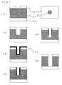
- FIG. 1 is a series of cross-sectional views as well as a bird's eye view in explaining the steps of First Embodiment.[0074]
- There is provided a[0075]
silicon substrate 100 on which apolysilicon film 102 that is to be used as a hard mask for etching is formed, overlying anoxide silicon film 101. - Next, by means of photolithography, an opening is set in a photoresist formed on the[0076]
polysilicon 102 and, through that opening, thepolysilicon 102 is dry etched to form a hard mask for etching. After that, the photoresist is removed (FIG. 1(1)) - The[0077]
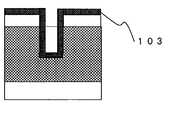
polysilicon 102 can be replaced by Si3N4, SiGe or Ge. - Through the hard mask, a first etching is applied thereto and a hole (an opening section) with an aspect ratio of 7 to 12 where no bowing occurs is formed in the silicon oxide film[0078]101 (FIG. 1(2)). Next, a Si3N4film103 is formed by the low pressure CVD method (FIG. 1(3)). Instead of the Si3N4film, a silicon oxynitride film, a polysilicon film, a SiGe film or a Ge film can be used.
- Next, the entire surface thereof is dry etched and the Si[0079]3N4film103 formed on the
polysilicon 102 and on the bottom face of the hole is removed (FIG. 1(4)). - The Si[0080]3N4film103 remaining on the sidewall of the hole is required to cover at least in the place of the hole corresponding to the aspect ratios of 2 to 7 where the bowing is liable to occur. After that, by applying a second etching thereto, the Si3N4film103 remaining on the lateral face of the hole is removed, while the
silicon oxide film 101 is dry etched (FIG. 1(5)), and an opening to reach thesilicon substrate 100 is formed (FIG. 1(6)). - FIG. 1([0081]5) herein is a view depicting a state in which the Si3N4film103 is etched simultaneously with the
silicon oxide film 101 by the second etching. - In the present embodiment, by the entire surface etching (in the case that the entire surface etching and the second etching have the same etching conditions, the initial state of the second etching), the Si[0082]3N4film103 is etched back and a sidewall of the Si3N4film is formed on the surface of the hole wall. The side wall Si3N4film is simultaneously removed when the silicon oxide film is etched still deeper by the second etching. If the sidewall Si3N4film is completely etched away before formation of the hole to reach the
silicon substrate 100 is completed, a bowing may occur so that the thickness of the Si3N4film must be set appropriately so as not to allow such a thing happening. - Apart from the film thickness of the Si[0083]3N4film, the condition of the etching selection ratio between the Si3N4film and the silicon oxide film can be met, needless to say, by a set of two different conditions, etching conditions for the entire surface etching of the Si3N4film and etching conditions for the etching of the silicon oxide film.
- In the present embodiment, since, even if a hole to reach the silicon substrate is formed and its aspect ratio exceeds the aspect ratio of 13 with which a bowing is liable to occur, the very place of the hole wall surface where the bowing is liable to occur is covered with the Si[0084]3N4film whose etching selection ratio is lower than that of the oxide film, the hole wall surface cannot be subjected to the aberrant etching till the Si3N4film is removed and no bowing develops.
- Although the[0085]
silicon oxide film 101 in FIG. 1 is formed immediately above thesilicon substrate 100, it goes without saying that a semiconductor element, an interconnection, an insulating film or the like formed on asilicon substrate 100 can be laid under thesilicon oxide film 101. - To suppress the bowing from developing in the opening by the second etching, the etching rate in the horizontal direction for the Si[0086]3N4film is preferably equal to or less than {fraction (1/10)} of the etching rate in the horizontal direction for the silicon oxide film.
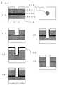
- A modified embodiment of First Embodiment is shown in FIG. 2.[0087]
- In FIG. 2, there is formed a Si[0088]3N4film104, which is to function as an etching stopper, between a first silicon oxide film101-1 and a second silicon oxide film101-2.
- The silicon oxide films[0089]101-1 and101-2 can be made of silicon oxide being formed by the CVD method, non-doped silicate glass, silicate glass containing at least either of boron and phosphorus or silicon oxide which is formed by sintering a coating of siloxane applied thereto by the spin-on-glass method.
- As shown in FIG. 1([0090]1), a
polysilicon film 102 is set to be used as a hard mask for dry etching (FIG. 2(1)) and an oxide film101-2 being dry etched by a first dry etching, a hole is formed so as to reach a Si3N4film104 (FIG. 2(2)). Next, a Si3N4film103 is formed by the low pressure CVD method (FIG. 2(3)). - Next, the entire surface thereof is dry etched and the Si[0091]3N4film103 formed on the
polysilicon 102 and on the bottom face of the hole as well as the Si3N4film104 lying on the bottom face of the hole, which acts as an etching stopper, are removed (FIG. 2(4)). After that, by applying a second etching thereto, the Si3N4film103 remaining on the wall surface of the hole is removed, while the silicon oxide film101-1 is dry etched (FIG. 2(5)) and an opening to reach thesilicon substrate 100 is formed (FIG. 2(6)). - Needless to say, the entire surface dry etching and the second dry etching can be performed continuously under the same conditions.[0092]
- In the present embodiment, at the time of the first etching, because etching is stopped at the etching stopper layer, overetching does not happen. Accordingly, it is possible to provide some extra time in the step of bringing the etching to a halt. Further, anisotropic etching normally forms the diameter at the hole bottom narrower than that at the top of the hole. When an etching stopper layer is set, etching in the direction of the depth is stopped once and thereafter etching in the horizontal direction starts at the hole bottom, and, therefore, the cross-section of the hole can take the form of more regular rectangle.[0093]
- In the present embodiment, in the second half of the hole etching of the silicon oxide film when a bowing is liable to occur, a sidewall Si[0094]3N4film is provided for the upper section of the hole which is the very place that the bowing is liable to appear so that the bowing can be prevented or suppressed from occurring. The sidewall Si3N4film formed on the sidewall of the hole may be removed while the silicon oxide film101-1 is etched in the second half of the second hole etching.
- In the above description of the present embodiment, the Si[0095]3N4film formed on the sidewall of the hole is completely removed when the formation of the hole is accomplished. However, in the case of a via hole for connecting an upper layer interconnection with a lower layer interconnection, the Si3N4film can be left on the wall surface of the hole.
- If the situation allows the Si[0096]3N4film to remain on the wall surface of the hole, the Si3N4film103 can be formed to have a substantial thickness.
- The material of the sidewall formed on the wall surface of the hole can be, apart from the Si[0097]3N4film, any material whose etching rate is lower than the etching rate of the material that is to be used to fill up the hole, and must be appropriately chosen, depending on the hole filling material.
- In the case that the hole filling material is a silicon oxide film, a silicon oxynitride film, a polysilicon film, a SiGe film, a Ge film or the like can be used as the sidewall material, apart from a Si[0098]3N4film.
- As First Example of the present invention, a manufacturing method of a cylindrical capacitor of a DRAM is described below, referring to FIG. 5.[0099]
- On a[0100]
silicon substrate 100, a Si3N4film105 that is to be used as a bottom film of a cylindrical capacitor when formed is grown by the low pressure CVD method and thereon asilicon oxide film 101 that is to be used as a capacitor film of the cylindrical capacitor is formed to a thickness of 2 μm by the low pressure CVD method. - An underlying layer of the Si[0101]3N4film105 that is to function as a bottom film of the cylindrical capacitor varies with the structure of the DRAM but, herein, it is omitted because it is not particularly related to the present example.
- The thickness of the silicon oxide film or the depth of the hole into which a cylindrical capacitor is to be formed is the parameter of the utmost importance to determine the amount of the capacitance of the cylindrical capacitor. Viewed in the light of device characteristics, a large capacitance is normally preferable so that the film thickness is set to be as thick as possible within the range of the workable thickness and, thus, not limited to 2 μm.[0102]
- As a hard mask, a[0103]
polysilicon film 102 with a thickness of 100 nm to 150 nm is grown immediately above thesilicon oxide film 101. This film functions as a mask when dry etching is applied to the silicon oxide film, and may be a film made of a material with an etching rate lower than that of the silicon oxide film. Apart from polysilicon, doped polysilicon, Si3N4, SiGe, Ge or such can be employed therefor. - These silicon oxide films and polysilicon films can be formed also by the plasma CVD method.[0104]
- Next, patterning (exposure, development and such) is carried out by a known technique of lithography. When the minimum diameter of the hole pattern is 0.15 μm, the aspect ratio becomes 13.3 (2 μm/0.15 m=13.3).[0105]
- Next, using a photoresist as a mask, dry etching for formation of a polysilicon hard mask is performed. After dry etching, remaining photoresists, etching deposition residuals and the likes are removed with a SPM (a mixed solution of sulfuric acid and hydrogen peroxide), an APM (a mixed solution of ammonia and hydrogen peroxide), a diluted hydrofluoric acid solution or the like.[0106]
- These dry etching conditions for the polysilicon are ordinary ones and an anisotropic etching treatment may be made with a chlorine-based mixed gas, a mixed gas containing HBr or the like.[0107]
- Next, a treatment is made using a two-frequency type RIE (Reactive Ion Etching) apparatus shown in FIG. 6. The apparatus is characterized by the presence of two types of RF (Radio Frequency) generators, providing an upper band of RF frequencies between 13.56 MHz and 100 MHz and a lower band of RF frequencies between 400 KHz and 2 MHz, and, in recent years, has been used widely by the present inventors.[0108]
- Firstly, a first etching of the silicon oxide film is performed. The details of the conditions are as follows.[0109]
- Wafer susceptor temperature: 40° C. to 60° C.[0110]
- C[0111]4F8(Fluorocarbon gas such as C5F8, C4F6can be also used): 20 sccm to 40 sccm (standard cubic centimeters minute)
- Ar: 500 sccm to 800 sccm[0112]
- O[0113]2: 20 sccm to 40 sccm
- Upper RF: 1000 W to 2000W[0114]
- Lower RF: 1000 W to 2000 W[0115]
- Under these conditions, the etching rate ratio in the direction of the depth, that is, the etching rate of the oxide film/the etching rate of the Si[0116]3N4film is approximately 10, while the etching rate ratio in the horizontal direction is approximately 20.
- After the first etching of the silicon oxide film, a state shown in FIG. 5([0117]2) is obtained. The depth possible to be etched while keeping a bowingless state corresponds to an aspect ratio of 7 to 12. In other words, in the present example with an aperture of 0.15 μm, down to a depth of 1.05 μm to 1.8 μm a bowing does not occur. Accordingly, the depth for the first etching of the silicon oxide film may be set to be 1.05 μm to 1.8 μm. Meanwhile, in a hole with an aspect ratio of 12 or greater, the place where a bowing occurs has a depth equivalent to aspect ratios of 2 to 7, and when an aperture of the hole is 0.15 μm, this corresponds to a region at depths of 300 nm to 1.05 μm. It is this place a bowing is liable to occur that a sidewall which is to be set in the next step is required to be formed. In effect, when the depth of the first etching is set to be 1.05 μm to 1.8 μm, the sidewall Si3N4film which is to be formed in the next step can be optimally set in the very place where a bowing is liable to occur when the second etching is made.
- In the present example, the etching was carried our for the time period calculated from the etching rate so as to reach the depth of 1.5 μm or so.[0118]
- Under the first etching conditions, fluorocarbon gas is employed. The dry etching with fluorocarbon gas is liable to leave fluorocarbon-based deposition residuals on the wafer surface. It is therefore preferable to remove, after the etching, reaction products using the plasma peeling-off method or a solution such as a diluted hydrofluoric acid solution, an APM or a SPM.[0119]
- Next, a Si[0120]3N4film with a thickness of 4 nm is formed by the low pressure CVD method so as to have a uniform thickness (FIG. 5(3)). For this, it is also possible to use any other method than the low pressure CVD method as long as a film of dense quality (excelling in etching resistance) with a capability to provide good coverage (a high conformability) can be obtained.
- In the present example, a Si[0121]3N4film with a thickness of 4 nm was formed. This can be explained from a fact that, in removing the silicon oxide by the second etching, if the Si3N4film formed on the wall surface of the hole is removed prior to the completion of the hole, there occurs a bowing. The actual thickness of the Si3N4film is determined, depending on the conditions of the second etching, but a film thickness of 2 nm to 5 nm is, in general, suitable.
- At the time the opening just reaches the[0122]
silicon substrate 100, the opening is taper-shaped. The aperture of the opening on the side of the substrate is narrow and the contact resistance, when filled up, becomes high. Overetching is preferably performed until the aperture of the opening on the side of the substrate becomes the same as that of the top. The film thickness is, therefore, preferably set, taking overetching into consideration. The film thickness of 4 nm set in the present example is the one obtained under the condition that overetching is performed for approximately 20 seconds after the hole reaches thesilicon substrate 100. The overetching condition differs in etching conditions as well as the etching apparatus and it is apparent that an actual value must be set appropriately, independent of the value obtained in the present example. - Next, applying dry etching to the entire surface thereof, portions of the Si[0123]3N4film103 formed on the surface of the polysilicon that is to be used as a hard mask as well as on the bottom of the hole are removed (FIG. 5(4)). After that, second dry etching is performed consecutively to remove the
silicon oxide 101 and form a hole down to reach the Si3N4film105 that is to become a bottom film of a cylindrical capacitor (FIG. 5(5)). In the present example, the opening which is not taper-shaped but rectangular was successfully formed. - In the present example, for the entire surface dry etching and the second etching, the same conditions as for the first etching are employed.[0124]
- In this way, formation of a hole for a bowingless cylindrical capacitor with a high aspect ratio can be accomplished.[0125]
- Referring to FIG. 9, Second Example, which is a modified example of First Example, is described below.[0126]
- In FIG. 9, differing from in FIG. 5, a Si[0127]3N4film104, which is to function as an etching stopper, is formed in a
layer 101 of silicon oxide through which a hole for a cylindrical capacitor is formed. - On a[0128]
silicon substrate 100, a Si3N4film105 that is to be used as a bottom film of a cylindrical capacitor when formed is grown by the low pressure CVD method and thereon a lower layer of silicon oxide101-1 with a thickness of 0.5 μm, a Si3N4layer104 with a thickness of 15 nm which is to function as an etching stopper, an upper layer of silicon oxide101-2 with a thickness of 1.5 μm and apolysilicon film 102 with a thickness of 100 nm which is to be used as a hard mask are formed, in this order, by the low pressure CVD method or the plasma CVD method. - An underlying layer of the Si[0129]3N4film105 that is to function as a bottom film of the cylindrical capacitor varies with the structure of the DRAM but, herein, it is omitted because it is not particularly related to the present example.
- The thickness of the silicon oxide film or the depth of the hole into which a cylindrical capacitor is to be formed is the parameter of the utmost importance to determine the amount of the capacitance of the cylindrical capacitor. Viewed in the light of device characteristics, a large capacitance is normally preferable so that the film thickness is set to be as thick as possible within the range of the workable thickness, and although the combined thicknesses of the upper layer of silicon oxide and the lower layer of silicon oxide herein is 2 μm, they are not necessarily limited to this thickness.[0130]
- The[0131]
polysilicon film 102 with a thickness of 100 nm, which is to be used as a hard mask, functions as a mask when dry etching is applied to the silicon oxide film. For this, a film made of a material with an etching rate lower than that of the silicon oxide film is chosen, and, apart from polysilicon, doped polysilicon, Si3N4, SiGe, Ge or such can be employed therefor. - Next, patterning (exposure, development and such) is carried out by a known technique of lithography. When the minimum diameter of the hole pattern is 0.15 μm, the aspect ratio becomes 13.3 (2 μm/0.15 μm=13.3).[0132]
- Next, using a photoresist as a mask, dry etching for formation of a polysilicon hard mask is performed. After dry etching, remaining photoresists, etching deposition residuals and the likes are removed with a SPM (Sulfuric Peroxide Mix) (a mixed solution of sulfuric acid and hydrogen peroxide), an APM (Ammonia Peroxide Mix) (a mixed solution of ammonia and hydrogen peroxide), a diluted hydrofluoric acid solution or the like.[0133]
- These dry etching conditions for the polysilicon are ordinary ones and an anisotropic etching treatment may be made with a chlorine-based mixed gas, a mixed gas containing HBr or the like.[0134]
- Next, a treatment is made using a two-frequency type RIE (Reactive Ion Etching) apparatus shown in FIG. 6. The apparatus is characterized by the presence of two types of RF (Radio Frequency) generators, providing an upper band of RF frequencies between 13.56 MHz and 100 MHz and a lower band of RF frequencies between 400 KHz and 2 MHz, and, in recent years, has been used widely by the present inventors.[0135]
- Firstly, a first etching of the silicon oxide film is performed. The details of the conditions are as follows.[0136]
- Wafer susceptor temperature: 40° C. to 60° C.[0137]
- C[0138]4F8(Fluorocarbon gas such as C5F8, C4F6can be also used): 20 sccm to 40 sccm
- Ar: 500 sccm to 800 sccm[0139]
- O[0140]2: 20 sccm to 40 sccm
- Upper RF: 1000 W to 2000W[0141]
- Lower RF: 1000 W to 2000 W[0142]
- After the first etching of the silicon oxide film, a state shown in FIG. 9([0143]2) is obtained. The depth possible to be etched while keeping a bowingless state corresponds to an aspect ratio of 7 to 12. In other words, in the present example with an aperture of 0.15 μm, down to a depth of 1.05 μm to 1.8 μm a bowing does not occur. Accordingly, the film thickness of the upper layer of silicon oxide101-2 may be set to be 1.5 μm and, immediately under the upper layer of silicon oxide101-2, a Si3N4film104 which is to act as an etching stopper may be formed.
- Meanwhile, in a hole with an aspect ratio of 12 or greater, the place where a bowing occurs has a depth equivalent to aspect ratios of 2 to 7. When an aperture of the hole is 0.15 μm, this corresponds to a region at depths of 300 nm to 1.05 μm, and it is this place a bowing is liable to occur that a sidewall which is to be set in the next step is required to be formed. In effect, when the depth of the first etching is set to be 1.05 μm to 1.8 μm, the sidewall Si[0144]3N4film which is to be formed in the next step can be optimally set in the very place where a bowing is liable to occur when the second etching is made.
- In the present example, the etching stopper is formed at a depth of 1.5 μm.[0145]
- In the present example, because the Si[0146]3N4film104 is formed to function as an etching stopper, even if extra first etching time period is provided, the etching does not proceed deeper than designed. It is, therefore, possible to give some extra time to the first etching time period. Further, this etching stopper has the effect of preventing excessive etching to take place even if the etching rate increases due to a change in etching conditions.
- Under the first etching conditions, fluorocarbon gas is employed. The dry etching with fluorocarbon gas is liable to leave fluorocarbon-based deposition residuals on the wafer surface. It is therefore preferable to remove, after the etching, reaction products using the plasma peeling-off method or a solution such as a diluted hydrofluoric acid solution, an APM or a SPM.[0147]
- Next, a Si[0148]3N4film with a thickness of 10 nm is formed by the low pressure CVD method so as to have a uniform thickness (FIG. 9(3)). The thickness of the Si3N4film is optimally 5 nm to 15 nm. Further, it is also possible to use any other method than the low pressure CVD method as long as a film of dense quality (excelling in etching resistance) with a capability to provide good coverage (a high conformability) can be obtained.
- In the present example, a Si[0149]3N4film with a thickness of 2 nm to 5 nm was formed. This can be explained from a fact that, in removing the silicon oxide by the second etching, if the Si3N4film formed on the wall surface of the hole is removed prior to the completion of the hole, there occurs a bowing. The actual thickness of the Si3N4film is determined, depending on the conditions of the second etching.
- Next, applying dry etching to the entire surface thereof, portions of the Si[0150]3N4film103 formed on the surface of the polysilicon that is to be used as a hard mask as well as on the bottom of the hole are removed (FIG. 9(4)). After that, second dry etching is consecutively applied thereto through the polysilicon hard mask to remove the
silicon oxide 101 and form a hole down to reach the Si3N4film105 that is to become a bottom film of a cylindrical capacitor (FIG. 9(5)). In the present example, too, overetching was performed for approximately 20 seconds after the opening reached thesilicon substrate 100, and thereby modification of the taper-like shape was made. - In the present example, for the entire surface dry etching and the second etching, the same conditions as for the first etching are employed.[0151]
- In this way, formation of a hole for a bowingless cylindrical capacitor with a high aspect ratio can be accomplished.[0152]
- As Third Example of the present invention, a manufacturing method of a contact hole (a hole interconnection running in the vertical direction and connecting an interconnection with a Si substrate) or a via hole (a hole interconnection running in the vertical direction and connecting an upper layer interconnection layer with a lower layer interconnection layer) shown in FIG. 8 is described below.[0153]
- In recent years, the semiconductor integrated circuit device has become large in scale, and the multi-layered interconnection with three layers or more is commonly in use. In FIG. 8, there is shown an example of a double-layered interconnection, comprising a semiconductor element or an interconnection formed on a silicon substrate and interconnections formed on two layer levels. In this case, when the interconnection on the second layer level is connected with the interconnection lying on the substrate, an aspect ratio of a hole exceeds 13 and a bowing may occur therein. Because the spacing of the neighbouring interconnections is narrow, when the bowing occurs, the interconnections in neighbouring contact holes may make a short circuit. Further, even if no short-circuit is made, the distance between the neighbouring contact holes become shorter than designed so that the parasitic capacitance increases and the device characteristics deteriorate.[0154]
- Now, referring to FIG. 10, the present example is described below.[0155]
- While a manufacturing method of a via hole to connect an interconnection on the first layer level with an interconnection on the third layer level (not shown in the drawings) is shown in FIG. 10, it is apparent that the method is not limited to the case shown therein.[0156]
- There are comprised a first interconnection[0157]111 and a second interlayer insulating film112 formed on a first
interlayer insulating film 110; a second interconnection113 formed on the second interlayer insulating film112; a third interlayer insulating film114 formed on the second interconnection113; and apolysilicon film 115 formed on the third interlayer insulating film114, which is to be used as a hard mask for etching. - The first[0158]
interlayer insulating film 110, the second interlayer insulating film112 and the third interlayer insulating film114 are each a silicon oxide film with a thickness of 1.5 μm. The first interconnection111 and the second interconnection113 are each an interconnection of polysilicon doped with dopants. The interconnections can be also made of TiN, W, AlCu, Ti, CoSi, TiSi or such. Thepolysilicon film 115 that is to be used as a hard mask for etching is an insulating film with a thickness of 100 nm to 150 nm into which no dopants are doped. The silicon oxide films and the polysilicon films are formed by the low pressure CVD method or the plasma CVD method. - A hard mask for etching made of polysilicon is used as a mask in etching the silicon oxide films, and, therefore, without being limited to polysilicon, can utilize any material having a high etching selection ratio to the silicon oxide film. Examples for the material include, apart from polysilicon, a silicon nitride film (Si[0159]3N4film), a silicon oxynitride film, a SiGe film and a Ge film.
- Next, patterning (exposure, development and such) is carried out by a known technique of lithography. A hole pattern with a diameter of 0.2 μm is formed (FIG. 10([0160]11)).
- Next, using a photoresist as a mask, etching for formation of a polysilicon hard mask is performed. After etching, remaining photoresists, etching deposition residuals and the likes are removed with a SPM or such.[0161]
- The dry etching conditions for the polysilicon are ordinary ones and a treatment may be made under the conditions of a chlorine-based mixed gas, a mixed gas containing HBr or the like.[0162]
- Next, a treatment is made using a two-frequency type RIE (Reactive Ion Etching) apparatus shown in FIG. 6. The apparatus is characterized by the presence of two types of RF (Radio Frequency) generators, providing an upper band of RF frequencies between 13.56 MHz and 100 MHz and a lower band of RF frequencies between 400 KHz and 2 MHz, and, in recent years, has been used widely by the present inventors.[0163]
- A first etching of the silicon oxide film is then performed. The details of the conditions are as follows.[0164]
- Wafer susceptor temperature: 40° C. to 60° C.[0165]
- C[0166]4F8(Fluorocarbon gas such as C5F8, C4F6can be also used): 20 sccm to 40 sccm
- Ar: 500 sccm to 800 sccm[0167]
- O[0168]2: 20 sccm to 40 sccm
- Upper RF: 1000 W to 2000W[0169]
- Lower RF: 1000 W to 2000 W[0170]
- After the first etching of the silicon oxide film, a state shown in FIG. 10([0171]2) is obtained.
- The depth possible to be etched while keeping a bowingless state corresponds to an aspect ratio of 7 to 12. In other words, in the present example with an aperture of 0.2 μm, down to a depth of 1.4 μm to 2.4 μm a bowing does not occur. Accordingly, the depth for the first etching of the silicon oxide film may be set to be 1.4 μm to 2.4 μm.[0172]
- In the present example, a hole with a depth of 2.0 μm was formed by the first silicon oxide etching.[0173]
- Under the first etching conditions, fluorocarbon gas is employed. The dry etching with fluorocarbon gas is liable to leave fluorocarbon-based deposition residuals on the wafer surface. It is therefore preferable to remove, after the etching, reaction products using the plasma peeling-off method or a solution such as a diluted hydrofluoric acid solution, an APM or a SPM.[0174]
- Next, a Si[0175]3N4film116 with a thickness of 20 nm is formed by the low pressure CVD method so as to have a uniform thickness (FIG. 10(3)). For this, it is also possible to use any other method than the low pressure CVD method as long as a film of dense quality (excelling in etching resistance) with a capability to provide good coverage (a high conformability) can be obtained.
- Next, the entire surface etching is applied onto the Si[0176]3N4film under the following conditions and portions of the Si3N4film103 lying on the surface of the
polysilicon film 115 as well as on the bottom of the hole are removed (FIG. 10(4)). - Wafer susceptor temperature: 40° C. to 60° C.[0177]
- C[0178]4F8(or CHF3): 30 sccm to 100 sccm
- Ar: 200 sccm[0179]
- O[0180]2: 15 sccm to 50 sccm
- Upper RF: 1000 W to 2000W[0181]
- Lower RF: 1000 W to 2000 W[0182]
- The reason why the etching conditions for the entire surface etching are changed from the etching conditions for First Example, Second Example and first etching and second etching of Third Example solely lies in a fact that a nitride film in this case is formed considerably thick. With the above conditions, the etching rate of the nitride film is set high. It is a matter of course that, in the case that the etching time period is not particularly limited, the etching conditions for the entire surface etching can be the same as those for the first silicon oxide etching and the second silicon oxide etching.[0183]
- Under these above conditions, the etching rate ratio in the direction of the depth, that is, the etching rate of the oxide film/the etching rate of the Si[0184]3N4film is approximately 5.
- After that, under the same conditions for the first silicon oxide etching, the second silicon oxide etching is carried out, and, thereby, the formation of a via hole is accomplished (FIG. 10([0185]6)).
- While the Si[0186]3N4film in First Example is 2 nm to 5 nm in thickness, the Si3N4film in Third Example is 20 nm in thickness. Further, in First Example and Second Example, the Si3N4films formed on the sidewalls are thoroughly removed, but, in Third Example, the film is etched by mere 2 nm to 5 nm (FIG. 10(5)).
- This results in a via hole having an aperture of approximately 0.15 μm, which is narrower than the aperture of 0.2 μm the hard mask has.[0187]
- This makes the aspect ratio of the finished via hole[0188]20 (3 μm/0.15 μm=20). Meanwhile, the height corresponding to the aspect ratios of 7 to 20, with which the bowing is liable to occur is 1.05 μm to 1.8 μm, and on the sidewall of the hole in this region, the Si3N4film116 still remains. In effect, a bowingless via hole with a high aspect ratio can be obtained.
Claims (22)
Applications Claiming Priority (2)
| Application Number | Priority Date | Filing Date | Title |
|---|---|---|---|
| JP2003-125106 | 2003-04-30 | ||
| JP2003125106AJP3976703B2 (en) | 2003-04-30 | 2003-04-30 | Manufacturing method of semiconductor device |
Publications (2)
| Publication Number | Publication Date |
|---|---|
| US20040219780A1true US20040219780A1 (en) | 2004-11-04 |
| US7122463B2 US7122463B2 (en) | 2006-10-17 |
Family
ID=33308160
Family Applications (1)
| Application Number | Title | Priority Date | Filing Date |
|---|---|---|---|
| US10/834,247Expired - Fee RelatedUS7122463B2 (en) | 2003-04-30 | 2004-04-29 | Manufacturing method of semiconductor device |
Country Status (2)
| Country | Link |
|---|---|
| US (1) | US7122463B2 (en) |
| JP (1) | JP3976703B2 (en) |
Cited By (72)
| Publication number | Priority date | Publication date | Assignee | Title |
|---|---|---|---|---|
| US20040036126A1 (en)* | 2002-08-23 | 2004-02-26 | Chau Robert S. | Tri-gate devices and methods of fabrication |
| US20050218438A1 (en)* | 2004-03-31 | 2005-10-06 | Nick Lindert | Bulk non-planar transistor having strained enhanced mobility and methods of fabrication |
| US20060084268A1 (en)* | 2004-10-15 | 2006-04-20 | Martin Verhoeven | Method for production of charge-trapping memory cells |
| US20070001219A1 (en)* | 2005-06-30 | 2007-01-04 | Marko Radosavljevic | Block contact architectures for nanoscale channel transistors |
| US20070004194A1 (en)* | 2005-06-30 | 2007-01-04 | Yong-Tae Cho | Method for fabricating semiconductor device with deep opening |
| US20070090416A1 (en)* | 2005-09-28 | 2007-04-26 | Doyle Brian S | CMOS devices with a single work function gate electrode and method of fabrication |
| US20070123031A1 (en)* | 2005-11-30 | 2007-05-31 | Elpida Memory, Inc | Method for production of semiconductor device |
| US7241653B2 (en) | 2003-06-27 | 2007-07-10 | Intel Corporation | Nonplanar device with stress incorporation layer and method of fabrication |
| US7268058B2 (en) | 2004-01-16 | 2007-09-11 | Intel Corporation | Tri-gate transistors and methods to fabricate same |
| US20080044970A1 (en)* | 2006-08-18 | 2008-02-21 | Promos Technologies Inc. | Memory structure and method for preparing the same |
| US7348284B2 (en) | 2004-08-10 | 2008-03-25 | Intel Corporation | Non-planar pMOS structure with a strained channel region and an integrated strained CMOS flow |
| US20080102634A1 (en)* | 2006-10-31 | 2008-05-01 | Texas Instruments Incorporated | Sacrificial CMP etch stop layer |
| US7396711B2 (en) | 2005-12-27 | 2008-07-08 | Intel Corporation | Method of fabricating a multi-cornered film |
| US7402875B2 (en) | 2005-08-17 | 2008-07-22 | Intel Corporation | Lateral undercut of metal gate in SOI device |
| US7449373B2 (en) | 2006-03-31 | 2008-11-11 | Intel Corporation | Method of ion implanting for tri-gate devices |
| US7456476B2 (en) | 2003-06-27 | 2008-11-25 | Intel Corporation | Nonplanar semiconductor device with partially or fully wrapped around gate electrode and methods of fabrication |
| US7479421B2 (en) | 2005-09-28 | 2009-01-20 | Intel Corporation | Process for integrating planar and non-planar CMOS transistors on a bulk substrate and article made thereby |
| US7518196B2 (en) | 2005-02-23 | 2009-04-14 | Intel Corporation | Field effect transistor with narrow bandgap source and drain regions and method of fabrication |
| US7547637B2 (en) | 2005-06-21 | 2009-06-16 | Intel Corporation | Methods for patterning a semiconductor film |
| US7550333B2 (en) | 2004-10-25 | 2009-06-23 | Intel Corporation | Nonplanar device with thinned lower body portion and method of fabrication |
| US20090170276A1 (en)* | 2007-12-27 | 2009-07-02 | Hynix Semiconductor Inc. | Method of Forming Trench of Semiconductor Device |
| US7579280B2 (en)* | 2004-06-01 | 2009-08-25 | Intel Corporation | Method of patterning a film |
| US7825038B2 (en) | 2006-05-30 | 2010-11-02 | Applied Materials, Inc. | Chemical vapor deposition of high quality flow-like silicon dioxide using a silicon containing precursor and atomic oxygen |
| US7859053B2 (en) | 2004-09-29 | 2010-12-28 | Intel Corporation | Independently accessed double-gate and tri-gate transistors in same process flow |
| US7858481B2 (en) | 2005-06-15 | 2010-12-28 | Intel Corporation | Method for fabricating transistor with thinned channel |
| US7867923B2 (en) | 2007-10-22 | 2011-01-11 | Applied Materials, Inc. | High quality silicon oxide films by remote plasma CVD from disilane precursors |
| US7879675B2 (en) | 2005-03-14 | 2011-02-01 | Intel Corporation | Field effect transistor with metal source/drain regions |
| US7902080B2 (en)* | 2006-05-30 | 2011-03-08 | Applied Materials, Inc. | Deposition-plasma cure cycle process to enhance film quality of silicon dioxide |
| US7935643B2 (en) | 2009-08-06 | 2011-05-03 | Applied Materials, Inc. | Stress management for tensile films |
| US7943531B2 (en) | 2007-10-22 | 2011-05-17 | Applied Materials, Inc. | Methods for forming a silicon oxide layer over a substrate |
| US7989365B2 (en) | 2009-08-18 | 2011-08-02 | Applied Materials, Inc. | Remote plasma source seasoning |
| US7989280B2 (en) | 2005-11-30 | 2011-08-02 | Intel Corporation | Dielectric interface for group III-V semiconductor device |
| US7994019B1 (en) | 2010-04-01 | 2011-08-09 | Applied Materials, Inc. | Silicon-ozone CVD with reduced pattern loading using incubation period deposition |
| US8084818B2 (en) | 2004-06-30 | 2011-12-27 | Intel Corporation | High mobility tri-gate devices and methods of fabrication |
| US8232176B2 (en) | 2006-06-22 | 2012-07-31 | Applied Materials, Inc. | Dielectric deposition and etch back processes for bottom up gapfill |
| US8236708B2 (en) | 2010-03-09 | 2012-08-07 | Applied Materials, Inc. | Reduced pattern loading using bis(diethylamino)silane (C8H22N2Si) as silicon precursor |
| US8304351B2 (en) | 2010-01-07 | 2012-11-06 | Applied Materials, Inc. | In-situ ozone cure for radical-component CVD |
| US8318584B2 (en) | 2010-07-30 | 2012-11-27 | Applied Materials, Inc. | Oxide-rich liner layer for flowable CVD gapfill |
| US8329262B2 (en) | 2010-01-05 | 2012-12-11 | Applied Materials, Inc. | Dielectric film formation using inert gas excitation |
| US8357435B2 (en) | 2008-05-09 | 2013-01-22 | Applied Materials, Inc. | Flowable dielectric equipment and processes |
| US8362566B2 (en) | 2008-06-23 | 2013-01-29 | Intel Corporation | Stress in trigate devices using complimentary gate fill materials |
| US8445078B2 (en) | 2011-04-20 | 2013-05-21 | Applied Materials, Inc. | Low temperature silicon oxide conversion |
| US8449942B2 (en) | 2009-11-12 | 2013-05-28 | Applied Materials, Inc. | Methods of curing non-carbon flowable CVD films |
| US8450191B2 (en) | 2011-01-24 | 2013-05-28 | Applied Materials, Inc. | Polysilicon films by HDP-CVD |
| US8466073B2 (en) | 2011-06-03 | 2013-06-18 | Applied Materials, Inc. | Capping layer for reduced outgassing |
| US8476142B2 (en) | 2010-04-12 | 2013-07-02 | Applied Materials, Inc. | Preferential dielectric gapfill |
| US8524004B2 (en) | 2010-06-16 | 2013-09-03 | Applied Materials, Inc. | Loadlock batch ozone cure |
| US8551891B2 (en) | 2011-10-04 | 2013-10-08 | Applied Materials, Inc. | Remote plasma burn-in |
| US8563445B2 (en) | 2010-03-05 | 2013-10-22 | Applied Materials, Inc. | Conformal layers by radical-component CVD |
| US8614149B2 (en)* | 2005-05-31 | 2013-12-24 | Lam Research Corporation | Critical dimension reduction and roughness control |
| US8617945B2 (en) | 2006-08-02 | 2013-12-31 | Intel Corporation | Stacking fault and twin blocking barrier for integrating III-V on Si |
| US8617989B2 (en) | 2011-09-26 | 2013-12-31 | Applied Materials, Inc. | Liner property improvement |
| US8629067B2 (en) | 2009-12-30 | 2014-01-14 | Applied Materials, Inc. | Dielectric film growth with radicals produced using flexible nitrogen/hydrogen ratio |
| US8647992B2 (en) | 2010-01-06 | 2014-02-11 | Applied Materials, Inc. | Flowable dielectric using oxide liner |
| US8664127B2 (en) | 2010-10-15 | 2014-03-04 | Applied Materials, Inc. | Two silicon-containing precursors for gapfill enhancing dielectric liner |
| US8716154B2 (en) | 2011-03-04 | 2014-05-06 | Applied Materials, Inc. | Reduced pattern loading using silicon oxide multi-layers |
| US8741788B2 (en) | 2009-08-06 | 2014-06-03 | Applied Materials, Inc. | Formation of silicon oxide using non-carbon flowable CVD processes |
| US8889566B2 (en) | 2012-09-11 | 2014-11-18 | Applied Materials, Inc. | Low cost flowable dielectric films |
| US8980382B2 (en) | 2009-12-02 | 2015-03-17 | Applied Materials, Inc. | Oxygen-doping for non-carbon radical-component CVD films |
| US9018108B2 (en) | 2013-01-25 | 2015-04-28 | Applied Materials, Inc. | Low shrinkage dielectric films |
| US9285168B2 (en) | 2010-10-05 | 2016-03-15 | Applied Materials, Inc. | Module for ozone cure and post-cure moisture treatment |
| US9404178B2 (en) | 2011-07-15 | 2016-08-02 | Applied Materials, Inc. | Surface treatment and deposition for reduced outgassing |
| US9412581B2 (en) | 2014-07-16 | 2016-08-09 | Applied Materials, Inc. | Low-K dielectric gapfill by flowable deposition |
| CN106856163A (en)* | 2016-11-22 | 2017-06-16 | 上海华力微电子有限公司 | A kind of forming method of high aspect ratio figure structure |
| US10068787B2 (en)* | 2016-12-30 | 2018-09-04 | Sunpower Corporation | Bowing semiconductor wafers |
| US10283321B2 (en) | 2011-01-18 | 2019-05-07 | Applied Materials, Inc. | Semiconductor processing system and methods using capacitively coupled plasma |
| US10832950B2 (en)* | 2019-02-07 | 2020-11-10 | International Business Machines Corporation | Interconnect with high quality ultra-low-k dielectric |
| KR20210066989A (en)* | 2019-11-28 | 2021-06-08 | 삼성전자주식회사 | Three-dimensional semiconductor memory device |
| CN113192831A (en)* | 2020-01-29 | 2021-07-30 | 东京毅力科创株式会社 | Etching method, substrate processing apparatus, and substrate processing system |
| JP2021118347A (en)* | 2020-01-29 | 2021-08-10 | 東京エレクトロン株式会社 | Etching method, substrate processing equipment, and substrate processing system |
| CN114628323A (en)* | 2022-05-05 | 2022-06-14 | 长鑫存储技术有限公司 | Manufacturing method of semiconductor structure and semiconductor structure |
| US12009228B2 (en) | 2015-02-03 | 2024-06-11 | Applied Materials, Inc. | Low temperature chuck for plasma processing systems |
Families Citing this family (20)
| Publication number | Priority date | Publication date | Assignee | Title |
|---|---|---|---|---|
| US7105390B2 (en) | 2003-12-30 | 2006-09-12 | Intel Corporation | Nonplanar transistors with metal gate electrodes |
| JP4211674B2 (en) | 2004-05-12 | 2009-01-21 | セイコーエプソン株式会社 | Semiconductor device and manufacturing method thereof, electro-optical device and manufacturing method thereof, and electronic apparatus |
| US7332439B2 (en) | 2004-09-29 | 2008-02-19 | Intel Corporation | Metal gate transistors with epitaxial source and drain regions |
| US7361958B2 (en) | 2004-09-30 | 2008-04-22 | Intel Corporation | Nonplanar transistors with metal gate electrodes |
| KR100605510B1 (en)* | 2004-12-14 | 2006-07-31 | 삼성전자주식회사 | Manufacturing method of flash memory device having control gate extension |
| US7476604B1 (en)* | 2005-05-13 | 2009-01-13 | Advanced Micro Devices, Inc. | Aggressive cleaning process for semiconductor device contact formation |
| JP2007081383A (en)* | 2005-08-15 | 2007-03-29 | Fujitsu Ltd | Microstructure manufacturing method |
| KR100809324B1 (en) | 2006-02-07 | 2008-03-05 | 삼성전자주식회사 | Semiconductor device and manufacturing method thereof |
| US7608195B2 (en)* | 2006-02-21 | 2009-10-27 | Micron Technology, Inc. | High aspect ratio contacts |
| JP2007258233A (en)* | 2006-03-20 | 2007-10-04 | Oki Electric Ind Co Ltd | Semiconductor device, manufacturing method thereof, and circuit board |
| JP5161503B2 (en)* | 2007-07-09 | 2013-03-13 | ルネサスエレクトロニクス株式会社 | Manufacturing method of semiconductor device |
| KR100965030B1 (en)* | 2007-10-10 | 2010-06-21 | 주식회사 하이닉스반도체 | Method for forming contact plug of semiconductor device and semiconductor device |
| KR101497546B1 (en) | 2008-11-06 | 2015-03-03 | 삼성전자주식회사 | Method of fabricating semiconductor device with spacer in SAC |
| CN103443906B (en)* | 2011-03-04 | 2016-03-30 | 应用材料公司 | How to clean the contacts |
| US8304916B1 (en) | 2011-07-06 | 2012-11-06 | Northrop Grumman Systems Corporation | Half-through vias for suppression of substrate modes |
| KR102106259B1 (en) | 2013-08-16 | 2020-05-04 | 삼성전자 주식회사 | Method for forming a trench of semiconductor device |
| JP6549765B2 (en)* | 2014-06-16 | 2019-07-24 | 東京エレクトロン株式会社 | Processing method |
| JP6373150B2 (en)* | 2014-06-16 | 2018-08-15 | 東京エレクトロン株式会社 | Substrate processing system and substrate processing method |
| JP2020009840A (en)* | 2018-07-04 | 2020-01-16 | 東京エレクトロン株式会社 | Etching method and substrate processing apparatus |
| US12112954B2 (en) | 2020-01-29 | 2024-10-08 | Tokyo Electron Limited | Etching method, substrate processing apparatus, and substrate processing system |
Citations (3)
| Publication number | Priority date | Publication date | Assignee | Title |
|---|---|---|---|---|
| US6200735B1 (en)* | 1998-04-07 | 2001-03-13 | Oki Electric Industry Co., Ltd. | Method for forming contact hole by dry etching |
| US6255161B1 (en)* | 2000-10-06 | 2001-07-03 | Nanya Technology Corporation | Method of forming a capacitor and a contact plug |
| US6300238B1 (en)* | 1999-08-03 | 2001-10-09 | United Microelectronics Corp. | Method of fabricating node contact opening |
Family Cites Families (4)
| Publication number | Priority date | Publication date | Assignee | Title |
|---|---|---|---|---|
| SG54548A1 (en) | 1996-08-28 | 1998-11-16 | Texas Instruments Inc | Contact formation for a semiconductor device |
| US5940731A (en) | 1996-10-16 | 1999-08-17 | Vanguard International Semiconductor Corp. | Method for forming tapered polysilicon plug and plug formed |
| JPH10294367A (en) | 1997-04-21 | 1998-11-04 | Sony Corp | Manufacture of semiconductor device |
| JP3897071B2 (en) | 1998-01-20 | 2007-03-22 | ソニー株式会社 | Manufacturing method of semiconductor device |
- 2003
- 2003-04-30JPJP2003125106Apatent/JP3976703B2/ennot_activeExpired - Fee Related
- 2004
- 2004-04-29USUS10/834,247patent/US7122463B2/ennot_activeExpired - Fee Related
Patent Citations (3)
| Publication number | Priority date | Publication date | Assignee | Title |
|---|---|---|---|---|
| US6200735B1 (en)* | 1998-04-07 | 2001-03-13 | Oki Electric Industry Co., Ltd. | Method for forming contact hole by dry etching |
| US6300238B1 (en)* | 1999-08-03 | 2001-10-09 | United Microelectronics Corp. | Method of fabricating node contact opening |
| US6255161B1 (en)* | 2000-10-06 | 2001-07-03 | Nanya Technology Corporation | Method of forming a capacitor and a contact plug |
Cited By (130)
| Publication number | Priority date | Publication date | Assignee | Title |
|---|---|---|---|---|
| US20070281409A1 (en)* | 2002-08-23 | 2007-12-06 | Yuegang Zhang | Multi-gate carbon nano-tube transistors |
| US20050199950A1 (en)* | 2002-08-23 | 2005-09-15 | Chau Robert S. | Tri-gate devices and methods of fabrication |
| US7560756B2 (en) | 2002-08-23 | 2009-07-14 | Intel Corporation | Tri-gate devices and methods of fabrication |
| US7514346B2 (en) | 2002-08-23 | 2009-04-07 | Intel Corporation | Tri-gate devices and methods of fabrication |
| US20060228840A1 (en)* | 2002-08-23 | 2006-10-12 | Chau Robert S | Tri-gate devices and methods of fabrication |
| US7504678B2 (en) | 2002-08-23 | 2009-03-17 | Intel Corporation | Tri-gate devices and methods of fabrication |
| US7427794B2 (en) | 2002-08-23 | 2008-09-23 | Intel Corporation | Tri-gate devices and methods of fabrication |
| US20040036126A1 (en)* | 2002-08-23 | 2004-02-26 | Chau Robert S. | Tri-gate devices and methods of fabrication |
| US7368791B2 (en) | 2002-08-23 | 2008-05-06 | Intel Corporation | Multi-gate carbon nano-tube transistors |
| US7358121B2 (en) | 2002-08-23 | 2008-04-15 | Intel Corporation | Tri-gate devices and methods of fabrication |
| US7820513B2 (en) | 2003-06-27 | 2010-10-26 | Intel Corporation | Nonplanar semiconductor device with partially or fully wrapped around gate electrode and methods of fabrication |
| US7241653B2 (en) | 2003-06-27 | 2007-07-10 | Intel Corporation | Nonplanar device with stress incorporation layer and method of fabrication |
| US8273626B2 (en) | 2003-06-27 | 2012-09-25 | Intel Corporationn | Nonplanar semiconductor device with partially or fully wrapped around gate electrode and methods of fabrication |
| US7714397B2 (en) | 2003-06-27 | 2010-05-11 | Intel Corporation | Tri-gate transistor device with stress incorporation layer and method of fabrication |
| US8405164B2 (en) | 2003-06-27 | 2013-03-26 | Intel Corporation | Tri-gate transistor device with stress incorporation layer and method of fabrication |
| US7456476B2 (en) | 2003-06-27 | 2008-11-25 | Intel Corporation | Nonplanar semiconductor device with partially or fully wrapped around gate electrode and methods of fabrication |
| US7268058B2 (en) | 2004-01-16 | 2007-09-11 | Intel Corporation | Tri-gate transistors and methods to fabricate same |
| US7781771B2 (en) | 2004-03-31 | 2010-08-24 | Intel Corporation | Bulk non-planar transistor having strained enhanced mobility and methods of fabrication |
| US7326634B2 (en) | 2004-03-31 | 2008-02-05 | Intel Corporation | Bulk non-planar transistor having strained enhanced mobility and methods of fabrication |
| US20050218438A1 (en)* | 2004-03-31 | 2005-10-06 | Nick Lindert | Bulk non-planar transistor having strained enhanced mobility and methods of fabrication |
| US7579280B2 (en)* | 2004-06-01 | 2009-08-25 | Intel Corporation | Method of patterning a film |
| US8084818B2 (en) | 2004-06-30 | 2011-12-27 | Intel Corporation | High mobility tri-gate devices and methods of fabrication |
| US7348284B2 (en) | 2004-08-10 | 2008-03-25 | Intel Corporation | Non-planar pMOS structure with a strained channel region and an integrated strained CMOS flow |
| US7960794B2 (en) | 2004-08-10 | 2011-06-14 | Intel Corporation | Non-planar pMOS structure with a strained channel region and an integrated strained CMOS flow |
| US8399922B2 (en) | 2004-09-29 | 2013-03-19 | Intel Corporation | Independently accessed double-gate and tri-gate transistors |
| US7859053B2 (en) | 2004-09-29 | 2010-12-28 | Intel Corporation | Independently accessed double-gate and tri-gate transistors in same process flow |
| US8268709B2 (en) | 2004-09-29 | 2012-09-18 | Intel Corporation | Independently accessed double-gate and tri-gate transistors in same process flow |
| US20060084268A1 (en)* | 2004-10-15 | 2006-04-20 | Martin Verhoeven | Method for production of charge-trapping memory cells |
| US7550333B2 (en) | 2004-10-25 | 2009-06-23 | Intel Corporation | Nonplanar device with thinned lower body portion and method of fabrication |
| US8749026B2 (en) | 2004-10-25 | 2014-06-10 | Intel Corporation | Nonplanar device with thinned lower body portion and method of fabrication |
| US8067818B2 (en) | 2004-10-25 | 2011-11-29 | Intel Corporation | Nonplanar device with thinned lower body portion and method of fabrication |
| US9190518B2 (en) | 2004-10-25 | 2015-11-17 | Intel Corporation | Nonplanar device with thinned lower body portion and method of fabrication |
| US9741809B2 (en) | 2004-10-25 | 2017-08-22 | Intel Corporation | Nonplanar device with thinned lower body portion and method of fabrication |
| US8502351B2 (en) | 2004-10-25 | 2013-08-06 | Intel Corporation | Nonplanar device with thinned lower body portion and method of fabrication |
| US10236356B2 (en) | 2004-10-25 | 2019-03-19 | Intel Corporation | Nonplanar device with thinned lower body portion and method of fabrication |
| US7893506B2 (en) | 2005-02-23 | 2011-02-22 | Intel Corporation | Field effect transistor with narrow bandgap source and drain regions and method of fabrication |
| US8368135B2 (en) | 2005-02-23 | 2013-02-05 | Intel Corporation | Field effect transistor with narrow bandgap source and drain regions and method of fabrication |
| US8183646B2 (en) | 2005-02-23 | 2012-05-22 | Intel Corporation | Field effect transistor with narrow bandgap source and drain regions and method of fabrication |
| US8664694B2 (en) | 2005-02-23 | 2014-03-04 | Intel Corporation | Field effect transistor with narrow bandgap source and drain regions and method of fabrication |
| US7825481B2 (en) | 2005-02-23 | 2010-11-02 | Intel Corporation | Field effect transistor with narrow bandgap source and drain regions and method of fabrication |
| US9048314B2 (en) | 2005-02-23 | 2015-06-02 | Intel Corporation | Field effect transistor with narrow bandgap source and drain regions and method of fabrication |
| US7518196B2 (en) | 2005-02-23 | 2009-04-14 | Intel Corporation | Field effect transistor with narrow bandgap source and drain regions and method of fabrication |
| US8816394B2 (en) | 2005-02-23 | 2014-08-26 | Intel Corporation | Field effect transistor with narrow bandgap source and drain regions and method of fabrication |
| US9368583B2 (en) | 2005-02-23 | 2016-06-14 | Intel Corporation | Field effect transistor with narrow bandgap source and drain regions and method of fabrication |
| US7879675B2 (en) | 2005-03-14 | 2011-02-01 | Intel Corporation | Field effect transistor with metal source/drain regions |
| US8614149B2 (en)* | 2005-05-31 | 2013-12-24 | Lam Research Corporation | Critical dimension reduction and roughness control |
| US7858481B2 (en) | 2005-06-15 | 2010-12-28 | Intel Corporation | Method for fabricating transistor with thinned channel |
| US9806195B2 (en) | 2005-06-15 | 2017-10-31 | Intel Corporation | Method for fabricating transistor with thinned channel |
| US11978799B2 (en) | 2005-06-15 | 2024-05-07 | Tahoe Research, Ltd. | Method for fabricating transistor with thinned channel |
| US9337307B2 (en) | 2005-06-15 | 2016-05-10 | Intel Corporation | Method for fabricating transistor with thinned channel |
| US8933458B2 (en) | 2005-06-21 | 2015-01-13 | Intel Corporation | Semiconductor device structures and methods of forming semiconductor structures |
| US9761724B2 (en) | 2005-06-21 | 2017-09-12 | Intel Corporation | Semiconductor device structures and methods of forming semiconductor structures |
| US9385180B2 (en) | 2005-06-21 | 2016-07-05 | Intel Corporation | Semiconductor device structures and methods of forming semiconductor structures |
| US8071983B2 (en) | 2005-06-21 | 2011-12-06 | Intel Corporation | Semiconductor device structures and methods of forming semiconductor structures |
| US8581258B2 (en) | 2005-06-21 | 2013-11-12 | Intel Corporation | Semiconductor device structures and methods of forming semiconductor structures |
| US7547637B2 (en) | 2005-06-21 | 2009-06-16 | Intel Corporation | Methods for patterning a semiconductor film |
| US20070001219A1 (en)* | 2005-06-30 | 2007-01-04 | Marko Radosavljevic | Block contact architectures for nanoscale channel transistors |
| US7279375B2 (en) | 2005-06-30 | 2007-10-09 | Intel Corporation | Block contact architectures for nanoscale channel transistors |
| US20070004194A1 (en)* | 2005-06-30 | 2007-01-04 | Yong-Tae Cho | Method for fabricating semiconductor device with deep opening |
| US7898041B2 (en) | 2005-06-30 | 2011-03-01 | Intel Corporation | Block contact architectures for nanoscale channel transistors |
| US7402875B2 (en) | 2005-08-17 | 2008-07-22 | Intel Corporation | Lateral undercut of metal gate in SOI device |
| US7736956B2 (en) | 2005-08-17 | 2010-06-15 | Intel Corporation | Lateral undercut of metal gate in SOI device |
| US20070090416A1 (en)* | 2005-09-28 | 2007-04-26 | Doyle Brian S | CMOS devices with a single work function gate electrode and method of fabrication |
| US8294180B2 (en) | 2005-09-28 | 2012-10-23 | Intel Corporation | CMOS devices with a single work function gate electrode and method of fabrication |
| US8193567B2 (en) | 2005-09-28 | 2012-06-05 | Intel Corporation | Process for integrating planar and non-planar CMOS transistors on a bulk substrate and article made thereby |
| US7902014B2 (en) | 2005-09-28 | 2011-03-08 | Intel Corporation | CMOS devices with a single work function gate electrode and method of fabrication |
| US7479421B2 (en) | 2005-09-28 | 2009-01-20 | Intel Corporation | Process for integrating planar and non-planar CMOS transistors on a bulk substrate and article made thereby |
| US7595236B2 (en) | 2005-11-30 | 2009-09-29 | Elpida Memory, Inc. | Method for production of semiconductor device having a hole extending through a first insulating film, a second insulating film and a third insulating film |
| US20070123031A1 (en)* | 2005-11-30 | 2007-05-31 | Elpida Memory, Inc | Method for production of semiconductor device |
| US7989280B2 (en) | 2005-11-30 | 2011-08-02 | Intel Corporation | Dielectric interface for group III-V semiconductor device |
| US7396711B2 (en) | 2005-12-27 | 2008-07-08 | Intel Corporation | Method of fabricating a multi-cornered film |
| US7449373B2 (en) | 2006-03-31 | 2008-11-11 | Intel Corporation | Method of ion implanting for tri-gate devices |
| US7902080B2 (en)* | 2006-05-30 | 2011-03-08 | Applied Materials, Inc. | Deposition-plasma cure cycle process to enhance film quality of silicon dioxide |
| US7825038B2 (en) | 2006-05-30 | 2010-11-02 | Applied Materials, Inc. | Chemical vapor deposition of high quality flow-like silicon dioxide using a silicon containing precursor and atomic oxygen |
| US8232176B2 (en) | 2006-06-22 | 2012-07-31 | Applied Materials, Inc. | Dielectric deposition and etch back processes for bottom up gapfill |
| US8617945B2 (en) | 2006-08-02 | 2013-12-31 | Intel Corporation | Stacking fault and twin blocking barrier for integrating III-V on Si |
| US20080044970A1 (en)* | 2006-08-18 | 2008-02-21 | Promos Technologies Inc. | Memory structure and method for preparing the same |
| US8304342B2 (en)* | 2006-10-31 | 2012-11-06 | Texas Instruments Incorporated | Sacrificial CMP etch stop layer |
| US20080102634A1 (en)* | 2006-10-31 | 2008-05-01 | Texas Instruments Incorporated | Sacrificial CMP etch stop layer |
| US7867923B2 (en) | 2007-10-22 | 2011-01-11 | Applied Materials, Inc. | High quality silicon oxide films by remote plasma CVD from disilane precursors |
| US7943531B2 (en) | 2007-10-22 | 2011-05-17 | Applied Materials, Inc. | Methods for forming a silicon oxide layer over a substrate |
| US8242031B2 (en) | 2007-10-22 | 2012-08-14 | Applied Materials, Inc. | High quality silicon oxide films by remote plasma CVD from disilane precursors |
| US20090170276A1 (en)* | 2007-12-27 | 2009-07-02 | Hynix Semiconductor Inc. | Method of Forming Trench of Semiconductor Device |
| US8357435B2 (en) | 2008-05-09 | 2013-01-22 | Applied Materials, Inc. | Flowable dielectric equipment and processes |
| US9224754B2 (en) | 2008-06-23 | 2015-12-29 | Intel Corporation | Stress in trigate devices using complimentary gate fill materials |
| US9806193B2 (en) | 2008-06-23 | 2017-10-31 | Intel Corporation | Stress in trigate devices using complimentary gate fill materials |
| US9450092B2 (en) | 2008-06-23 | 2016-09-20 | Intel Corporation | Stress in trigate devices using complimentary gate fill materials |
| US8362566B2 (en) | 2008-06-23 | 2013-01-29 | Intel Corporation | Stress in trigate devices using complimentary gate fill materials |
| US8741733B2 (en) | 2008-06-23 | 2014-06-03 | Intel Corporation | Stress in trigate devices using complimentary gate fill materials |
| US8741788B2 (en) | 2009-08-06 | 2014-06-03 | Applied Materials, Inc. | Formation of silicon oxide using non-carbon flowable CVD processes |
| US7935643B2 (en) | 2009-08-06 | 2011-05-03 | Applied Materials, Inc. | Stress management for tensile films |
| US7989365B2 (en) | 2009-08-18 | 2011-08-02 | Applied Materials, Inc. | Remote plasma source seasoning |
| US8449942B2 (en) | 2009-11-12 | 2013-05-28 | Applied Materials, Inc. | Methods of curing non-carbon flowable CVD films |
| US8980382B2 (en) | 2009-12-02 | 2015-03-17 | Applied Materials, Inc. | Oxygen-doping for non-carbon radical-component CVD films |
| US8629067B2 (en) | 2009-12-30 | 2014-01-14 | Applied Materials, Inc. | Dielectric film growth with radicals produced using flexible nitrogen/hydrogen ratio |
| US8329262B2 (en) | 2010-01-05 | 2012-12-11 | Applied Materials, Inc. | Dielectric film formation using inert gas excitation |
| US8647992B2 (en) | 2010-01-06 | 2014-02-11 | Applied Materials, Inc. | Flowable dielectric using oxide liner |
| US8304351B2 (en) | 2010-01-07 | 2012-11-06 | Applied Materials, Inc. | In-situ ozone cure for radical-component CVD |
| US8563445B2 (en) | 2010-03-05 | 2013-10-22 | Applied Materials, Inc. | Conformal layers by radical-component CVD |
| US8236708B2 (en) | 2010-03-09 | 2012-08-07 | Applied Materials, Inc. | Reduced pattern loading using bis(diethylamino)silane (C8H22N2Si) as silicon precursor |
| US7994019B1 (en) | 2010-04-01 | 2011-08-09 | Applied Materials, Inc. | Silicon-ozone CVD with reduced pattern loading using incubation period deposition |
| US8476142B2 (en) | 2010-04-12 | 2013-07-02 | Applied Materials, Inc. | Preferential dielectric gapfill |
| US8524004B2 (en) | 2010-06-16 | 2013-09-03 | Applied Materials, Inc. | Loadlock batch ozone cure |
| US8318584B2 (en) | 2010-07-30 | 2012-11-27 | Applied Materials, Inc. | Oxide-rich liner layer for flowable CVD gapfill |
| US9285168B2 (en) | 2010-10-05 | 2016-03-15 | Applied Materials, Inc. | Module for ozone cure and post-cure moisture treatment |
| US8664127B2 (en) | 2010-10-15 | 2014-03-04 | Applied Materials, Inc. | Two silicon-containing precursors for gapfill enhancing dielectric liner |
| US10283321B2 (en) | 2011-01-18 | 2019-05-07 | Applied Materials, Inc. | Semiconductor processing system and methods using capacitively coupled plasma |
| US8450191B2 (en) | 2011-01-24 | 2013-05-28 | Applied Materials, Inc. | Polysilicon films by HDP-CVD |
| US8716154B2 (en) | 2011-03-04 | 2014-05-06 | Applied Materials, Inc. | Reduced pattern loading using silicon oxide multi-layers |
| US8445078B2 (en) | 2011-04-20 | 2013-05-21 | Applied Materials, Inc. | Low temperature silicon oxide conversion |
| US8466073B2 (en) | 2011-06-03 | 2013-06-18 | Applied Materials, Inc. | Capping layer for reduced outgassing |
| US9404178B2 (en) | 2011-07-15 | 2016-08-02 | Applied Materials, Inc. | Surface treatment and deposition for reduced outgassing |
| US8617989B2 (en) | 2011-09-26 | 2013-12-31 | Applied Materials, Inc. | Liner property improvement |
| US8551891B2 (en) | 2011-10-04 | 2013-10-08 | Applied Materials, Inc. | Remote plasma burn-in |
| US8889566B2 (en) | 2012-09-11 | 2014-11-18 | Applied Materials, Inc. | Low cost flowable dielectric films |
| US9018108B2 (en) | 2013-01-25 | 2015-04-28 | Applied Materials, Inc. | Low shrinkage dielectric films |
| US9412581B2 (en) | 2014-07-16 | 2016-08-09 | Applied Materials, Inc. | Low-K dielectric gapfill by flowable deposition |
| US12009228B2 (en) | 2015-02-03 | 2024-06-11 | Applied Materials, Inc. | Low temperature chuck for plasma processing systems |
| CN106856163A (en)* | 2016-11-22 | 2017-06-16 | 上海华力微电子有限公司 | A kind of forming method of high aspect ratio figure structure |
| US20180374730A1 (en)* | 2016-12-30 | 2018-12-27 | Sunpower Corporation | Bowing semiconductor wafers |
| US10720351B2 (en)* | 2016-12-30 | 2020-07-21 | Sunpower Corporation | Bowing semiconductor wafers |
| US10068787B2 (en)* | 2016-12-30 | 2018-09-04 | Sunpower Corporation | Bowing semiconductor wafers |
| US10832950B2 (en)* | 2019-02-07 | 2020-11-10 | International Business Machines Corporation | Interconnect with high quality ultra-low-k dielectric |
| KR20210066989A (en)* | 2019-11-28 | 2021-06-08 | 삼성전자주식회사 | Three-dimensional semiconductor memory device |
| KR102760678B1 (en)* | 2019-11-28 | 2025-02-04 | 삼성전자주식회사 | Three-dimensional semiconductor memory device |
| CN113192831A (en)* | 2020-01-29 | 2021-07-30 | 东京毅力科创株式会社 | Etching method, substrate processing apparatus, and substrate processing system |
| JP2021118347A (en)* | 2020-01-29 | 2021-08-10 | 東京エレクトロン株式会社 | Etching method, substrate processing equipment, and substrate processing system |
| CN113270315A (en)* | 2020-01-29 | 2021-08-17 | 东京毅力科创株式会社 | Etching method, substrate processing apparatus, and substrate processing system |
| JP7557969B2 (en) | 2020-01-29 | 2024-09-30 | 東京エレクトロン株式会社 | Etching method, substrate processing apparatus, and substrate processing system |
| CN114628323A (en)* | 2022-05-05 | 2022-06-14 | 长鑫存储技术有限公司 | Manufacturing method of semiconductor structure and semiconductor structure |
Also Published As
| Publication number | Publication date |
|---|---|
| JP2004335526A (en) | 2004-11-25 |
| JP3976703B2 (en) | 2007-09-19 |
| US7122463B2 (en) | 2006-10-17 |
Similar Documents
| Publication | Publication Date | Title |
|---|---|---|
| US7122463B2 (en) | Manufacturing method of semiconductor device | |
| US6306772B1 (en) | Deep trench bottle-shaped etching using Cl2 gas | |
| US7494934B2 (en) | Method of etching carbon-containing layer and method of fabricating semiconductor device | |
| US6071823A (en) | Deep trench bottle-shaped etch in centura mark II NG | |
| KR100288507B1 (en) | Manufacturing method of semiconductor device | |
| JPH0526337B2 (en) | ||
| JP4711658B2 (en) | Manufacturing method of semiconductor device having fine pattern | |
| US7122478B2 (en) | Method of manufacturing a semiconductor device using a polysilicon etching mask | |
| KR101078732B1 (en) | Method for fabricating semiconductoer device | |
| JP2000307001A (en) | Manufacture of semiconductor device | |
| JP4039504B2 (en) | Manufacturing method of semiconductor device | |
| US20080213967A1 (en) | Trench capacitor and method for manufacturing the same | |
| US20050136642A1 (en) | Method for fabricating semiconductor device | |
| US6566236B1 (en) | Gate structures with increased etch margin for self-aligned contact and the method of forming the same | |
| US7339253B2 (en) | Retrograde trench isolation structures | |
| JP2008004881A (en) | Method of manufacturing element isolation structure section | |
| US8034721B2 (en) | Manufacturing method of semiconductor device | |
| JPH0969511A (en) | Fabrication of semiconductor device | |
| US20080087950A1 (en) | Semiconductor device manufacturing method | |
| US7723229B2 (en) | Process of forming a self-aligned contact in a semiconductor device | |
| US6858452B2 (en) | Method for isolating self-aligned contact pads | |
| JPH11312730A (en) | Manufacturing method of semiconductor device | |
| KR0165453B1 (en) | Separation method of semiconductor device using Y-shaped trench | |
| JP2003158179A (en) | Semiconductor device and its fabricating method | |
| TWI744059B (en) | Methods for forming semiconductor devices |
Legal Events
| Date | Code | Title | Description |
|---|---|---|---|
| AS | Assignment | Owner name:ELPIDA MEMORY, INC, JAPAN Free format text:ASSIGNMENT OF ASSIGNORS INTEREST;ASSIGNOR:OHUCHI, MASAHIKO;REEL/FRAME:015276/0076 Effective date:20040423 | |
| FEPP | Fee payment procedure | Free format text:PAYOR NUMBER ASSIGNED (ORIGINAL EVENT CODE: ASPN); ENTITY STATUS OF PATENT OWNER: LARGE ENTITY | |
| FPAY | Fee payment | Year of fee payment:4 | |
| AS | Assignment | Owner name:ELPIDA MEMORY INC., JAPAN Free format text:SECURITY AGREEMENT;ASSIGNOR:PS4 LUXCO S.A.R.L.;REEL/FRAME:032414/0261 Effective date:20130726 | |
| FPAY | Fee payment | Year of fee payment:8 | |
| AS | Assignment | Owner name:PS4 LUXCO S.A.R.L., LUXEMBOURG Free format text:ASSIGNMENT OF ASSIGNORS INTEREST;ASSIGNOR:ELPIDA MEMORY, INC.;REEL/FRAME:032900/0568 Effective date:20130726 | |
| AS | Assignment | Owner name:PS5 LUXCO S.A.R.L., LUXEMBOURG Free format text:ASSIGNMENT OF ASSIGNORS INTEREST;ASSIGNOR:PS4 LUXCO S.A.R.L.;REEL/FRAME:039818/0506 Effective date:20130829 Owner name:LONGITUDE SEMICONDUCTOR S.A.R.L., LUXEMBOURG Free format text:CHANGE OF NAME;ASSIGNOR:PS5 LUXCO S.A.R.L.;REEL/FRAME:039793/0880 Effective date:20131112 | |
| FEPP | Fee payment procedure | Free format text:MAINTENANCE FEE REMINDER MAILED (ORIGINAL EVENT CODE: REM.) | |
| LAPS | Lapse for failure to pay maintenance fees | Free format text:PATENT EXPIRED FOR FAILURE TO PAY MAINTENANCE FEES (ORIGINAL EVENT CODE: EXP.); ENTITY STATUS OF PATENT OWNER: LARGE ENTITY | |
| STCH | Information on status: patent discontinuation | Free format text:PATENT EXPIRED DUE TO NONPAYMENT OF MAINTENANCE FEES UNDER 37 CFR 1.362 | |
| FP | Lapsed due to failure to pay maintenance fee | Effective date:20181017 |