US20040217391A1 - Localized strained semiconductor on insulator - Google Patents
Localized strained semiconductor on insulatorDownload PDFInfo
- Publication number
- US20040217391A1 US20040217391A1US10/425,797US42579703AUS2004217391A1US 20040217391 A1US20040217391 A1US 20040217391A1US 42579703 AUS42579703 AUS 42579703AUS 2004217391 A1US2004217391 A1US 2004217391A1
- Authority
- US
- United States
- Prior art keywords
- silicon
- region
- approximately
- strained
- layer
- Prior art date
- Legal status (The legal status is an assumption and is not a legal conclusion. Google has not performed a legal analysis and makes no representation as to the accuracy of the status listed.)
- Granted
Links
Images


Classifications
- H—ELECTRICITY
- H01—ELECTRIC ELEMENTS
- H01L—SEMICONDUCTOR DEVICES NOT COVERED BY CLASS H10
- H01L21/00—Processes or apparatus adapted for the manufacture or treatment of semiconductor or solid state devices or of parts thereof
- H01L21/02—Manufacture or treatment of semiconductor devices or of parts thereof
- H01L21/04—Manufacture or treatment of semiconductor devices or of parts thereof the devices having potential barriers, e.g. a PN junction, depletion layer or carrier concentration layer
- H01L21/18—Manufacture or treatment of semiconductor devices or of parts thereof the devices having potential barriers, e.g. a PN junction, depletion layer or carrier concentration layer the devices having semiconductor bodies comprising elements of Group IV of the Periodic Table or AIIIBV compounds with or without impurities, e.g. doping materials
- H01L21/26—Bombardment with radiation
- H01L21/263—Bombardment with radiation with high-energy radiation
- H01L21/265—Bombardment with radiation with high-energy radiation producing ion implantation
- H01L21/26506—Bombardment with radiation with high-energy radiation producing ion implantation in group IV semiconductors
- H01L21/26533—Bombardment with radiation with high-energy radiation producing ion implantation in group IV semiconductors of electrically inactive species in silicon to make buried insulating layers
- H—ELECTRICITY
- H01—ELECTRIC ELEMENTS
- H01L—SEMICONDUCTOR DEVICES NOT COVERED BY CLASS H10
- H01L21/00—Processes or apparatus adapted for the manufacture or treatment of semiconductor or solid state devices or of parts thereof
- H01L21/70—Manufacture or treatment of devices consisting of a plurality of solid state components formed in or on a common substrate or of parts thereof; Manufacture of integrated circuit devices or of parts thereof
- H01L21/71—Manufacture of specific parts of devices defined in group H01L21/70
- H01L21/76—Making of isolation regions between components
- H01L21/762—Dielectric regions, e.g. EPIC dielectric isolation, LOCOS; Trench refilling techniques, SOI technology, use of channel stoppers
- H01L21/7624—Dielectric regions, e.g. EPIC dielectric isolation, LOCOS; Trench refilling techniques, SOI technology, use of channel stoppers using semiconductor on insulator [SOI] technology
- H01L21/76243—Dielectric regions, e.g. EPIC dielectric isolation, LOCOS; Trench refilling techniques, SOI technology, use of channel stoppers using semiconductor on insulator [SOI] technology using silicon implanted buried insulating layers, e.g. oxide layers, i.e. SIMOX techniques
- H—ELECTRICITY
- H10—SEMICONDUCTOR DEVICES; ELECTRIC SOLID-STATE DEVICES NOT OTHERWISE PROVIDED FOR
- H10D—INORGANIC ELECTRIC SEMICONDUCTOR DEVICES
- H10D30/00—Field-effect transistors [FET]
- H10D30/60—Insulated-gate field-effect transistors [IGFET]
- H10D30/791—Arrangements for exerting mechanical stress on the crystal lattice of the channel regions
- H—ELECTRICITY
- H10—SEMICONDUCTOR DEVICES; ELECTRIC SOLID-STATE DEVICES NOT OTHERWISE PROVIDED FOR
- H10D—INORGANIC ELECTRIC SEMICONDUCTOR DEVICES
- H10D62/00—Semiconductor bodies, or regions thereof, of devices having potential barriers
- H10D62/10—Shapes, relative sizes or dispositions of the regions of the semiconductor bodies; Shapes of the semiconductor bodies
- H10D62/17—Semiconductor regions connected to electrodes not carrying current to be rectified, amplified or switched, e.g. channel regions
- H10D62/213—Channel regions of field-effect devices
- H10D62/221—Channel regions of field-effect devices of FETs
- H10D62/235—Channel regions of field-effect devices of FETs of IGFETs
- H10D62/292—Non-planar channels of IGFETs
- H—ELECTRICITY
- H10—SEMICONDUCTOR DEVICES; ELECTRIC SOLID-STATE DEVICES NOT OTHERWISE PROVIDED FOR
- H10D—INORGANIC ELECTRIC SEMICONDUCTOR DEVICES
- H10D84/00—Integrated devices formed in or on semiconductor substrates that comprise only semiconducting layers, e.g. on Si wafers or on GaAs-on-Si wafers
- H10D84/01—Manufacture or treatment
- H10D84/0123—Integrating together multiple components covered by H10D12/00 or H10D30/00, e.g. integrating multiple IGBTs
- H10D84/0126—Integrating together multiple components covered by H10D12/00 or H10D30/00, e.g. integrating multiple IGBTs the components including insulated gates, e.g. IGFETs
- H10D84/0165—Integrating together multiple components covered by H10D12/00 or H10D30/00, e.g. integrating multiple IGBTs the components including insulated gates, e.g. IGFETs the components including complementary IGFETs, e.g. CMOS devices
- H10D84/0167—Manufacturing their channels
- H—ELECTRICITY
- H10—SEMICONDUCTOR DEVICES; ELECTRIC SOLID-STATE DEVICES NOT OTHERWISE PROVIDED FOR
- H10D—INORGANIC ELECTRIC SEMICONDUCTOR DEVICES
- H10D84/00—Integrated devices formed in or on semiconductor substrates that comprise only semiconducting layers, e.g. on Si wafers or on GaAs-on-Si wafers
- H10D84/01—Manufacture or treatment
- H10D84/02—Manufacture or treatment characterised by using material-based technologies
- H10D84/03—Manufacture or treatment characterised by using material-based technologies using Group IV technology, e.g. silicon technology or silicon-carbide [SiC] technology
- H10D84/038—Manufacture or treatment characterised by using material-based technologies using Group IV technology, e.g. silicon technology or silicon-carbide [SiC] technology using silicon technology, e.g. SiGe
Definitions
- This disclosurerelates generally to semiconductor structures, and more particularly, to strained semiconductor on insulator structures.
- strained silicon and silicon on insulator technologiesTwo areas of interest for improving the speed and performance of semiconductor devices include strained silicon and silicon on insulator technologies. Strained silicon technology has been shown to enhance carrier mobility in both n and p-channel devices, and is being considered to improve the electron mobility and drift velocity in n-channel MOSFET's in CMOS technology. Silicon on insulator structures have been shown to reduce parasitic capacitances, and to increase switching speed of digital circuits and frequency in radio frequency (RF) circuits.
- RFradio frequency
- One technique for producing strained siliconinvolves growing silicon (Si) layers on relaxed silicon-germanium (SiGe) layers.
- Sisilicon
- SiGerelaxed silicon-germanium
- a large mismatch in the cell structure between the Si and SiGe layerscauses a pseudo-morphic layer of Si on relaxed SiGe to be under biaxial tensile strain.
- the biaxial strainmodifies the band structure and enhances carrier transport in the Si layer. For example, a 1% strain of the silicon layer almost doubles the electron mobility.
- One method for forming the strained Si layer on the relaxed SiGe layerinvolves epitaxially growing the Si and SiGe layers using an ultra-high vacuum chemical vapor deposition (UHVCVD) process, and is a costly and complex process.
- UHVCVDultra-high vacuum chemical vapor deposition
- a proposed back end approach for straining siliconapplies uniaxial strain to wafers/dies after the integrated circuit process is complete.
- the diesare thinned to membrane dimensions and then affixed to curved substrates to apply an in-plane, tensile strain after device manufacture.
- Another method for straining siliconforms voids in a transistor structure to produce a localized mechanical strain in the silicon.
- One technique for fabricating a silicon-on-insulator structureinvolves a SIMOX (Separation by IMplantation of OXygen-Silicon-On-Insulator) process.
- the SIMOX processuses a very high dose and high energy oxygen implant followed by an oxide growth to form a deep and thick buried oxide (BOX) region.
- the SIMOX processtypically forms a BOX region 3000 ⁇ thick or thicker.
- the silicon layer over the BOX regionis typically 1000 ⁇ or thicker.
- Various embodiments of the present inventionrelate to strained semiconductor films along with the structures and devices that include strained semiconductor films.
- Various embodiments of the present inventionfurther relate to methods of forming the strained semiconductor films along with methods of forming structures and devices that include strained semiconductor films.
- One aspectrelates to a method for straining a transistor body region.
- oxygen ionsare implanted to a predetermined depth in a localized region of a semiconductor substrate, and the substrate is annealed.
- Oxide growth within the semiconductor substrateforms a local oxide region within the semiconductor substrate.
- a portion of the substrateforms a semiconductor layer over the local oxide region.
- the semiconductor layerhas a thickness of approximately 300 ⁇ or less.
- the oxide growthstrains the semiconductor layer.
- An active region, including the body region, of the transistoris formed in the strained semiconductor layer.
- One aspectrelates to a transistor structure.
- Various embodiments of the transistorinclude a semiconductor substrate, and a localized insulator region formed within the substrate to partially separate a semiconductor layer from the semiconductor substrate.
- the semiconductor layerhas a strain induced by growth of the insulator region.
- the strained semiconductor layerhaving a thickness of approximately 300 ⁇ or less.
- First and second diffusion regionsare formed in the strained semiconductor layer over the insulator region. The first and second diffusion regions are separated by a body region in the strained semiconductor layer.
- a gateis positioned over the body region, and is separated from the body region by a gate dielectric.
- the semiconductor substrateincludes a silicon substrate, the strained semiconductor layer includes a strained silicon layer, and the insulator region includes an oxide region.
- the oxide regionis formed using a SIMOX (Separation by IMplantation of OXygen) process.
- the oxide regionis formed using a SPIMOX (Separation by Plasma IMplantation of OXygen) process.
- Various embodimentsprovide ultra-thin strained silicon body layers for n-channel CMOS transistors. Shallow oxygen implants are formed in a localized area to produce pockets of oxide under a surface layer of silicon. The silicon above the oxide pocket is stretched and strained by a heat treatment process and a resulting oxide growth.
- FIG. 1illustrates the lattice constant of a Si 1-X -Ge X substrate for different percentages (X) of Ge.
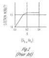
- FIG. 2illustrates the mobility enhancement for strained Si for different percentages (X) of Ge in a Si 1-X Ge X substrate.
- FIG. 3illustrates a relationship between elastic strain and semiconductor layer thicknesses.
- FIG. 4illustrates a process for forming shallow oxygen implants such as is used in a process to produce strained silicon body layers for n-channel CMOS transistors, according to various embodiments of the present invention.
- FIG. 5illustrates a process for forming a buried oxide (BOX) region from the shallow oxygen implants such as is used in a process to produce strained silicon body layers for n-channel CMOS transistors, according to various embodiments of the present invention.
- BOXburied oxide
- FIGS. 6A and 6Billustrate the strain in the semiconductor layer achieved by the process to produce strained silicon body layers for n-channel CMOS transistors illustrated in FIGS. 4 and 5.
- FIG. 7illustrates an n-channel CMOS transistor with a strained channel, according to various embodiments of the present invention.
- FIG. 8illustrates a method for forming a device with an ultra-thin strained semiconductor layer, according to various embodiments of the present invention.
- FIG. 9illustrates a method for growing a local insulator area in a substrate, according to various embodiments of the present invention.
- FIG. 10illustrates a method for forming a device with an ultra-thin semiconductor layer with an approximate uniform strain, according to various embodiments of the present invention.
- FIG. 11is a simplified block diagram of a high-level organization of various embodiments of a memory device according to various embodiments of the present invention.
- FIG. 12is a simplified block diagram of a high-level organization of various embodiments of an electronic system according to the present invention.
- wafer and substrateare interchangeably used to refer generally to any structure on which integrated circuits are formed, and also to such structures during various stages of integrated circuit fabrication. Both terms include doped and undoped semiconductors, epitaxial layers of a semiconductor on a supporting semiconductor or insulating material, combinations of such layers, as well as other such structures that are known in the art.
- Various embodimentsprovide a local semiconductor structure with a strained semiconductor layer on insulator.
- Various embodimentsprovide strained silicon body layers for n-channel transistors.
- Various embodimentsprovide advantages for CMOS transistors because of the strained semiconductor on insulator structure.
- Various embodimentsprovide a technique to produce ultra-thin strained silicon body layers over a local insulator.
- Mobilityis improved by straining semiconductor material.
- one technique for producing strained siliconinvolves growing silicon (Si) layers on relaxed silicon-germanium (SiGe) layers.
- Sihas a lattice constant of 5.43095 ⁇
- Gehas a lattice constant of 5.64613 ⁇ .
- the lattice constant of SiGeis between the lattice constant of Si and the lattice constant of Ge, and depends on the percentage of Ge in the SiGe layer.
- FIG. 1illustrates the lattice constant of a Si 1-X -Ge X substrate for different percentages (X) of Ge. As indicated by FIG.
- a Si 1-X Ge X substrate containing about 30% Ge (X ⁇ 0.3)has a lattice constant of about 5.50 ⁇ .
- FIG. 2illustrates the mobility enhancement for strained Si for different percentages (X) of Ge in a Si 1-X Ge X substrate.
- the mobility enhancementincreases as the percentage of Ge in the Si 1-X Ge X increases, and levels off to around 1.6 when the percentage of Ge is around 22% or larger.
- 22% Geprovides the Si 1-X Ge X substrate with a lattice constant (SiGe LC ) of around 5.485.
- SiGe LClattice constant
- FIG. 3illustrates a relationship between elastic strain and semiconductor layer thicknesses.
- the semiconductor yieldis plotted with respect to plastic deformation and defects in bulk samples.
- the illustrated valuesrepresent the relationship of thin SiGe layers on silicon.
- FIG. 3illustrates that thin layers of silicon or other semiconductor materials are more tolerant of strain than thick bulk samples.
- thin layers of SiGehave been fabricated on silicon because of the tolerance of the thin layers to strain.
- FIG. 3indicates that 300 ⁇ thin semiconductor layers can be strained up to about 2%.
- the mobility enhancement levels off when the strainreaches about 1%.
- a thin semiconductor layer with a strain greater than 0.5%it is desirable to strain a thin semiconductor layer with a strain greater than 0.5% to achieve significant mobility enhancement. It is desirable to strain a thin semiconductor layer, such as an ultra-thin layer approximately 300 ⁇ . or less, with a strain within a range of approximately 0.75% to approximately 1.5% where the mobility enhancement levels off. It is also desirable to reduce unnecessary strain and provide a margin for error without unduly affecting the mobility enhancement. Thus, it is desirable to strain a thin semiconductor layer with a strain in the range of approximately 1% to approximately 1.2%.
- silicon on insulator structureshave been shown to reduce parasitic capacitances, and to increase switching speed of digital circuits and frequency in radio frequency (RF) circuits.
- One technique for fabricating a silicon-on-insulator structureinvolves a SIMOX (Separation by IMplantation of OXygen-Silicon-On-Insulator) process.
- the SIMOX processuses a very high dose and high energy oxygen implant followed by an oxide growth to form a deep and thick buried oxide (BOX) region.
- the BOX regionis typically 3000 ⁇ thick or thicker and the silicon layer over the BOX region is typically 1000 ⁇ or thicker when the SIMOX process has been used.
- the SIMOX processis an expensive process.
- Various embodiments of the present inventionmechanically strain a thin semiconductor layer, and uses the mechanically-strained semiconductor in an active region of a device.
- the thin semiconductor layeris also referred to herein as an ultra- thin semiconductor layer.
- Various ultra-thin semiconductor layer embodimentshave a thickness of approximately 300 ⁇ or less.
- the semiconductor layeris mechanically strained by growing a local insulator region to partially separate the semiconductor layer from a semiconductor substrate.
- the local insulator regionis formed underneath where the active region of the device is to be formed.
- the amount of strain in the semiconductor layer over the local insulator regionis controlled by controlling the size and shape of the insulator region.
- a silicon layeris mechanically strained by growing a local oxide region in a silicon substrate to partially separate the silicon layer from a silicon substrate.
- FIG. 4illustrates a process for forming shallow oxygen implants such as is used in a process to produce strained silicon body layers for n-channel CMOS transistors, according to various embodiments of the present invention.
- a mask 402is formed over a silicon substrate 404 to define a local area corresponding to a desired location of a transistor.
- Oxygen ionsare implanted, as represented by the arrows 406 , to form shallow oxygen implants 408 .
- the range (R), or depth, of the oxygen implantsis 300 ⁇ or less to form an ultra-thin, strained silicon body layer upon completion of the process.
- the illustrated process for forming the shallow oxygen implantsinvolves a SIMOX process.
- the layer thicknesses illustrated in FIG. 4are much thinner than conventional SIMOX processes.
- Conventional SIMOXuse very high dose and high energy implants, which can cause an unacceptable amount of damage in the silicon surface layer.
- a silicon layer over the BOX regionis typically 1000 ⁇ or thicker, and the BOX region is typically 3000 ⁇ thick. These dimensions correspond to a large volume of oxide and high oxygen dose, typically of the order 10 18 /cm 2 and energies of 180 KeV.
- the illustrated process for forming the shallow oxygen implantsinvolves a SPIMOX (Separation by Plasma Implantation of Oxygen-Silicon-On-Insulator) process.
- SPIMOXSeparatation by Plasma Implantation of Oxygen-Silicon-On-Insulator
- a SPIMOX processonly requires an oxygen dose of the order 10 17 /cm 2 and energies of 60 KeV.
- SIMOX and SPIMOX processesto form oxygen implants and produce strained body layers in accordance with the present subject matter.
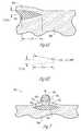
- FIG. 5illustrates a process for forming a buried oxide (BOX) region from the shallow oxygen implants such as is used in a process to produce strained silicon body layers for n-channel CMOS transistors, according to various embodiments of the present invention.
- the substrate 504is heat treated or annealed such that an oxide pocket 510 , also referred to herein as a BOX region, is formed by the localized shallow oxygen implants 408 shown in FIG. 4.
- the resulting oxide growthpartially separates a surface silicon layer 512 from the substrate 504 .
- the edges of the silicon layer 512remain attached to the substrate 504 .
- the growth of the BOX region 510strains this silicon layer 512 over the BOX region 510 .
- the illustrated silicon layer 512has a thickness T(Si), and the illustrated BOX region 510 has a thickness T(OX). Additionally, the footprint area of the BOX region 510 within the substrate 504 generally corresponds to the local area corresponding to the desired location of the transistor.
- the BOX region 510has a length L.
- the thickness of the silicon layeris an ultra-thin silicon layer corresponding to a thickness of 300 ⁇ or less.
- various embodimentsuse an oxide mask 402 with a tapered region or edge 414 proximate to the local area.
- the sloping oxide edge of the implant maskabsorbs some of the implanted oxygen such that fewer oxygen ions 406 penetrate the silicon substrate through the tapered region 414 , and those oxygen ions that do penetrate through the tapered region 414 penetrate the substrate 404 to a shallower depth, as represented by the portion 416 of the oxygen implants that extends closer to the substrate surface.
- the use of this tapered maskproduces a BOX region 510 with a tapered shape when the shallow oxygen implants 408 are annealed.
- the tapered mask and the implant processcan be engineered to provide a desired tapered shape of the resulting BOX region 510 to provide the silicon layer 512 over the BOX region 510 with a relatively uniform strain.
- FIGS. 6A and 6Billustrate the strain in the semiconductor layer achieved by the process to produce strained silicon body layers for n-channel CMOS transistors illustrated in FIGS. 4 and 5.
- a BOX region 610is formed in the substrate 604 at an average distance of about 325 ⁇ under the substrate surface.
- the illustrated BOX region 610has a length (L) of approximately 3000 ⁇ and a thickness (T(OX)) of about 450 ⁇ , such that the BOX region 610 extends from approximately 100 ⁇ to 550 ⁇ below the substrate surface.
- T(OX)thickness
- the growth of the BOX regiondisplaces the 100 ⁇ surface layer of silicon upwards by about 225 ⁇ (1 ⁇ 2 of T(OX)).
- the original length of the silicon layerincreases by a change ( ⁇ ) corresponding to the strain induced in the silicon layer.
- ⁇change
- half the length of the silicon layer (1 ⁇ 2 of L)increases by a ⁇ (strain). If the distance to the edge of the BOX region is 1500 ⁇ (1 ⁇ 2 of L), then it can be calculated that a 1.1% strain of the silicon surface layer results from the growth of the illustrated BOX region 610 that has a thickness of approximately 450 ⁇ and a length of approximately 3000 ⁇ .
- various embodiments of the present inventionare capable of mechanically straining the ultra-thin silicon layer within the desired range of approximately 1% to approximately 1.2% to achieve a desired mobility enhancement with an appropriate margin for error and without unnecessarily straining the ultra-thin silicon layer.
- FIG. 7illustrates an n-channel CMOS transistor with a strained channel, according to various embodiments of the present invention.
- Conventional techniquescan be used to from n-channel CMOS transistors with a strained silicon channel.
- the illustrated structureincludes a silicon substrate 704 with a local BOX region 710 formed therein at a location corresponding to the desired location of the transistor.
- the formation of the BOX region 710partially separates a silicon layer 712 , which can also be referred to as a surface silicon layer, from the remainder of the silicon substrate 704 .
- This silicon layer 712is strained.
- the illustrated BOX region 710has a tapered shape, which provides an approximate uniform strain to the silicon layer 712 .
- Conventional techniquescan be used to form the transistor 720 using the locally strained and insulated silicon layer 712 .
- Diffusion regions 722 and 724are formed in the strained silicon layer 712 over the local BOX region 710 .
- the diffusion regionsare implanted with n+ dopants.
- a strained body region 726is between the diffusion regions 722 and 724 .
- a gate 728is operably positioned over and separated from the strained body region 726 by a gate dielectric 730 .
- the illustrated structureshows a word (WL) line connected to the gate 728 and a bit line (BL) connected to one of the diffusion regions 722 .
- the strained body region 726is formed in an ultra-thin silicon layer having a thickness of approximately 300 ⁇ or less. In various embodiments, the strained body region 726 is formed in an ultra-thin silicon layer having a thickness of approximately 100 ⁇ or less. In various embodiments, the strained body region 726 is formed in an ultra-thin silicon layer having a thickness of approximately 50 ⁇ or less. In various embodiments, the strained body region 726 is formed in an ultra-thin silicon layer having a thickness within a range of approximately 20 ⁇ to approximately 30 ⁇ .
- FIG. 8illustrates a method for forming a device with an ultra-thin strained semiconductor layer, according to various embodiments of the present invention.
- a local insulator areasuch as an oxide region
- a gate dielectric and a gateare operably formed over the strained semiconductor layer. Formation of the diffusion regions at 844 and the gate dielectric and gate at 846 form a transistor using the strained semiconductor layer, as generally represented at 848 .
- FIG. 9illustrates a method for growing a local insulator area in a substrate, according to various embodiments of the present invention.
- a local insulator areais grown by implanting oxygen ions, as represented at 950 , and the substrate is annealed, as represented at 952 .
- Various embodimentsuse a SIMOX process, and various embodiments use a SPIMOX process to grow the local insulator area.
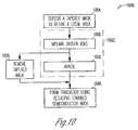
- FIG. 10illustrates a method for forming a device with an ultra-thin semiconductor layer with an approximate uniform strain, according to various embodiments of the present invention.
- a tapered maskis deposited on a substrate to define a local area where a transistor device is to be formed.
- a local insulator areais grown at 1042 .
- the local insulator areais grown by implanting oxygen ions into the local area of the substrate at 1050 , and annealing or heat-treating the substrate to grow an oxide at 1052 .
- the resulting growth of the oxideinduces a strain in a surface layer of silicon that is separated from the silicon substrate.
- the tapered maskis removed at an appropriate time in the process, and a transistor is formed using the resulting strained semiconductor layer at 1048 .
- FIG. 11is a simplified block diagram of a high-level organization of various embodiments of a memory device according to various embodiments of the present invention.
- the illustrated memory device 1168includes a memory array 1170 and read/write control circuitry 1172 to perform operations on the memory array via communication line(s) 1174 .
- the illustrated memory device 1168may be a memory card or a memory module such as a single inline memory module (SIMM) and dual inline memory module (DIMM).
- SIMMsingle inline memory module
- DIMMdual inline memory module
- semiconductor components in the memory array 1170 and/or the control circuitry 1172are able to be fabricated using the strained semiconductor films, as described above.
- the memory array 1170 and/or the control circuitry 1172include transistors with strained, ultra-thin body layers. The structure and fabrication methods for these strained, ultra-thin body layers have been described above.
- the memory array 1170includes a number of memory cells 1178 .
- the memory cells in the arrayare arranged in rows and columns.
- word lines 1180connect the memory cells in the rows
- bit lines 1182connect the memory cells in the columns.
- the read/write control circuitry 1172includes word line select circuitry 1174 , which functions to select a desired row.
- the read/write control circuitry 1172further includes bit line select circuitry 1176 , which functions to select a desired column.
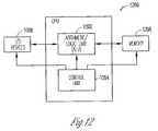
- FIG. 12is a simplified block diagram of a high-level organization of various embodiments of an electronic system according to the present invention.
- the system 1200is a computer system, a process control system or other system that employs a processor and associated memory.
- the electronic system 1200has functional elements, including a processor or arithmetic/logic unit (ALU) 1202 , a control unit 1204 , a memory device unit 1206 (such as illustrated in FIG. 11) and an input/output (I/O) device 1208 .
- ALUarithmetic/logic unit
- the control unit 1204coordinates all operations of the processor 1202 , the memory device 1206 and the I/O devices 1208 by continuously cycling through a set of operations that cause instructions to be fetched from the memory device 1206 and executed.
- the memory device 1206includes, but is not limited to, random access memory (RAM) devices, read-only memory (ROM) devices, and peripheral devices such as a floppy disk drive and a compact disk CD-ROM drive.
- RAMrandom access memory
- ROMread-only memory
- peripheral devicessuch as a floppy disk drive and a compact disk CD-ROM drive.
- the illustration of the system 1200is intended to provide a general understanding of one application for the structure and circuitry using embodiments of the present invention, and is not intended to serve as a complete description of all the elements and features of an electronic system.
- an electronic systemcan be fabricated in single-package processing units, or even on a single semiconductor chip, in order to reduce the communication time between the processor and the memory device.
- Applications containing strained semiconductor films, such as transistors with a strained ultra-thin semiconductor body layer, as described in this disclosureinclude electronic systems for use in memory modules, device drivers, power modules, communication modems, processor modules, and application-specific modules, and may include multilayer, multichip modules. Such circuitry can further be a subcomponent of a variety of electronic systems.
- Various embodiments disclosed hereinlocally grow an insulator region to partially separate and strain an upper or surface semiconductor layer of the substrate positioned over the insulator region.
- a locally strained semiconductor on a local insulator regionis provided.
- a SPIMOX or SIMOX processis used to form a local BOX region.
- a tapered maskis used to control the shape of the resulting BOX region to control the strain throughout the semiconductor layer.
- the locally strained semiconductor layeris used to form a transistor over the BOX region.
- the strained semiconductor on insulator devices disclosed hereinimprove the speed and performance of semiconductor devices through increased mobility and decreased stray capacitive loading.
Landscapes
- Physics & Mathematics (AREA)
- Engineering & Computer Science (AREA)
- High Energy & Nuclear Physics (AREA)
- Condensed Matter Physics & Semiconductors (AREA)
- General Physics & Mathematics (AREA)
- Manufacturing & Machinery (AREA)
- Computer Hardware Design (AREA)
- Microelectronics & Electronic Packaging (AREA)
- Power Engineering (AREA)
- Health & Medical Sciences (AREA)
- Toxicology (AREA)
- Thin Film Transistor (AREA)
Abstract
Description
- This application is related to the following commonly assigned U.S. patent applications which are herein incorporated by reference in their entirety: “Output Prediction Logic Circuits With Ultra-Thin Vertical Transistors and Methods of Formation,” U.S. application Ser. No. 10/164,611, filed on Jun. 10, 2002; “Micro-Mechanically Strained Semiconductor Film,” U.S. application Ser. No. ______, filed on (Attorney Docket 1303.089US1); “Strained Si/SiGe Layer Structures By Ion Implantation,” U.S. application Ser. No. ______, filed on ______ (Attorney Docket 1303.094US1); “Strained Silicon By A Twist/Tilt Misorientation In Wafer Bonding,” U.S. application Ser. No. ______, filed on ______ (Attorney Docket 1303.095US1); “Micromechanical Strained Silicon By Wafer Bonding,” U.S. application Ser. No. ______, filed on (Attorney Docket 1303.100US1).[0001]
- This disclosure relates generally to semiconductor structures, and more particularly, to strained semiconductor on insulator structures.[0002]
- Two areas of interest for improving the speed and performance of semiconductor devices include strained silicon and silicon on insulator technologies. Strained silicon technology has been shown to enhance carrier mobility in both n and p-channel devices, and is being considered to improve the electron mobility and drift velocity in n-channel MOSFET's in CMOS technology. Silicon on insulator structures have been shown to reduce parasitic capacitances, and to increase switching speed of digital circuits and frequency in radio frequency (RF) circuits.[0003]
- One technique for producing strained silicon involves growing silicon (Si) layers on relaxed silicon-germanium (SiGe) layers. A large mismatch in the cell structure between the Si and SiGe layers causes a pseudo-morphic layer of Si on relaxed SiGe to be under biaxial tensile strain. The biaxial strain modifies the band structure and enhances carrier transport in the Si layer. For example, a 1% strain of the silicon layer almost doubles the electron mobility. One method for forming the strained Si layer on the relaxed SiGe layer involves epitaxially growing the Si and SiGe layers using an ultra-high vacuum chemical vapor deposition (UHVCVD) process, and is a costly and complex process.[0004]
- A proposed back end approach for straining silicon applies uniaxial strain to wafers/dies after the integrated circuit process is complete. The dies are thinned to membrane dimensions and then affixed to curved substrates to apply an in-plane, tensile strain after device manufacture. Another method for straining silicon forms voids in a transistor structure to produce a localized mechanical strain in the silicon.[0005]
- One technique for fabricating a silicon-on-insulator structure involves a SIMOX (Separation by IMplantation of OXygen-Silicon-On-Insulator) process. The SIMOX process uses a very high dose and high energy oxygen implant followed by an oxide growth to form a deep and thick buried oxide (BOX) region. The SIMOX process typically forms a BOX region 3000 Å thick or thicker. The silicon layer over the BOX region is typically 1000 Å or thicker.[0006]
- There is a need in the art to provide improved semiconductor structures, and to provide methods of forming improved semiconductor structures, that improve the speed and performance of semiconductor devices through increased mobility and decreased stray capacitive loading.[0007]
- The above mentioned problems are addressed and will be understood by reading and studying this specification. Various embodiments of the present invention relate to strained semiconductor films along with the structures and devices that include strained semiconductor films. Various embodiments of the present invention further relate to methods of forming the strained semiconductor films along with methods of forming structures and devices that include strained semiconductor films.[0008]
- One aspect relates to a method for straining a transistor body region. In various embodiments, oxygen ions are implanted to a predetermined depth in a localized region of a semiconductor substrate, and the substrate is annealed. Oxide growth within the semiconductor substrate forms a local oxide region within the semiconductor substrate. A portion of the substrate forms a semiconductor layer over the local oxide region. The semiconductor layer has a thickness of approximately 300 Å or less. The oxide growth strains the semiconductor layer. An active region, including the body region, of the transistor is formed in the strained semiconductor layer.[0009]
- One aspect relates to a transistor structure. Various embodiments of the transistor include a semiconductor substrate, and a localized insulator region formed within the substrate to partially separate a semiconductor layer from the semiconductor substrate. The semiconductor layer has a strain induced by growth of the insulator region. The strained semiconductor layer having a thickness of approximately 300 Å or less. First and second diffusion regions are formed in the strained semiconductor layer over the insulator region. The first and second diffusion regions are separated by a body region in the strained semiconductor layer. A gate is positioned over the body region, and is separated from the body region by a gate dielectric.[0010]
- In various embodiments, the semiconductor substrate includes a silicon substrate, the strained semiconductor layer includes a strained silicon layer, and the insulator region includes an oxide region. In various embodiments, the oxide region is formed using a SIMOX (Separation by IMplantation of OXygen) process. In various embodiments, the oxide region is formed using a SPIMOX (Separation by Plasma IMplantation of OXygen) process. Various embodiments provide ultra-thin strained silicon body layers for n-channel CMOS transistors. Shallow oxygen implants are formed in a localized area to produce pockets of oxide under a surface layer of silicon. The silicon above the oxide pocket is stretched and strained by a heat treatment process and a resulting oxide growth.[0011]
- These and other aspects, embodiments, advantages, and features will become apparent from the following description and the referenced drawings.[0012]
- FIG. 1 illustrates the lattice constant of a Si[0013]1-X-GeXsubstrate for different percentages (X) of Ge.
- FIG. 2 illustrates the mobility enhancement for strained Si for different percentages (X) of Ge in a Si[0014]1-XGeXsubstrate.
- FIG. 3 illustrates a relationship between elastic strain and semiconductor layer thicknesses.[0015]
- FIG. 4 illustrates a process for forming shallow oxygen implants such as is used in a process to produce strained silicon body layers for n-channel CMOS transistors, according to various embodiments of the present invention.[0016]
- FIG. 5 illustrates a process for forming a buried oxide (BOX) region from the shallow oxygen implants such as is used in a process to produce strained silicon body layers for n-channel CMOS transistors, according to various embodiments of the present invention.[0017]
- FIGS. 6A and 6B illustrate the strain in the semiconductor layer achieved by the process to produce strained silicon body layers for n-channel CMOS transistors illustrated in FIGS. 4 and 5.[0018]
- FIG. 7 illustrates an n-channel CMOS transistor with a strained channel, according to various embodiments of the present invention.[0019]
- FIG. 8 illustrates a method for forming a device with an ultra-thin strained semiconductor layer, according to various embodiments of the present invention.[0020]
- FIG. 9 illustrates a method for growing a local insulator area in a substrate, according to various embodiments of the present invention.[0021]
- FIG. 10 illustrates a method for forming a device with an ultra-thin semiconductor layer with an approximate uniform strain, according to various embodiments of the present invention.[0022]
- FIG. 11 is a simplified block diagram of a high-level organization of various embodiments of a memory device according to various embodiments of the present invention.[0023]
- FIG. 12 is a simplified block diagram of a high-level organization of various embodiments of an electronic system according to the present invention.[0024]
- The following detailed description refers to the accompanying drawings which show, by way of illustration, specific aspects and embodiments in which the present invention may be practiced. The various embodiments are not necessarily mutually exclusive as aspects of one embodiment can be combined with aspects of another embodiment. Other embodiments may be utilized and structural, logical, and electrical changes may be made without departing from the scope of the present invention. In the following description, the terms wafer and substrate are interchangeably used to refer generally to any structure on which integrated circuits are formed, and also to such structures during various stages of integrated circuit fabrication. Both terms include doped and undoped semiconductors, epitaxial layers of a semiconductor on a supporting semiconductor or insulating material, combinations of such layers, as well as other such structures that are known in the art. The terms “horizontal” and “vertical”, as well as prepositions such as “on”, “side”, “over” and “under” are used in relation to the conventional plane or surface of a wafer or substrate, regardless of the orientation of the wafer or substrate. The following detailed description is, therefore, not to be taken in a limiting sense, and the scope of the present invention is defined only by the appended claims, along with the full scope of equivalents to which such claims are entitled.[0025]
- Various embodiments provide a local semiconductor structure with a strained semiconductor layer on insulator. Various embodiments provide strained silicon body layers for n-channel transistors. Various embodiments provide advantages for CMOS transistors because of the strained semiconductor on insulator structure. Various embodiments provide a technique to produce ultra-thin strained silicon body layers over a local insulator.[0026]
- Mobility is improved by straining semiconductor material. As noted earlier, one technique for producing strained silicon involves growing silicon (Si) layers on relaxed silicon-germanium (SiGe) layers. Si has a lattice constant of 5.43095 Å, and Ge has a lattice constant of 5.64613 Å. The lattice constant of SiGe is between the lattice constant of Si and the lattice constant of Ge, and depends on the percentage of Ge in the SiGe layer. FIG. 1 illustrates the lattice constant of a Si[0027]1-X-GeXsubstrate for different percentages (X) of Ge. As indicated by FIG. 1, a Si1-XGeXsubstrate containing about 30% Ge (X≈0.3) has a lattice constant of about 5.50 Å. The biaxial strain of the Si on the SiGe can be calculated as follows:

- FIG. 2 illustrates the mobility enhancement for strained Si for different percentages (X) of Ge in a Si[0029]1-XGeXsubstrate. The mobility enhancement increases as the percentage of Ge in the Si1-XGeXincreases, and levels off to around 1.6 when the percentage of Ge is around 22% or larger. Referring to FIG. 1, 22% Ge provides the Si1-XGeXsubstrate with a lattice constant (SiGeLC) of around 5.485. Using
Equation 1, it is determined that the corresponding strain for 22% Ge (the approximate point where the mobility enhancement levels off) is about 1%. - When the percentage of Ge in the Si[0030]1-XGeXis about 20% (near the knee of the curve), it can be calculated that the resulting strain is about 0.75%. When the percentage of Ge in the Si1-XGeXis about 40%, it can be calculated that the resulting strain is about 1.5%. Referring again to FIG. 1, it can be seen that a Si1-XGeXsubstrate having just under 10% Ge still provides considerable mobility enhancement (1.3). A Si1-XGeXsubstrate having just under 10% Ge provides the Si1-XGeXsubstrate with a lattice constant (SiGeLC) of around 5.457. Using
Equation 1, it is determined that the corresponding strain is around 0.5%. Thus, it is desirable to achieve a biaxial strain around or greater than 0.5%, and preferably around 1% or greater to obtain the desired enhanced mobility associated with strained Si. - Various embodiments of the present invention mechanically induce a strain in thin semiconductor layers, such as ultra thin silicon layers having a thickness around 300 Å or less. FIG. 3 illustrates a relationship between elastic strain and semiconductor layer thicknesses. The semiconductor yield is plotted with respect to plastic deformation and defects in bulk samples. The illustrated values represent the relationship of thin SiGe layers on silicon. FIG. 3 illustrates that thin layers of silicon or other semiconductor materials are more tolerant of strain than thick bulk samples. Previously, thin layers of SiGe have been fabricated on silicon because of the tolerance of the thin layers to strain. FIG. 3 indicates that 300 Å thin semiconductor layers can be strained up to about 2%. However, as illustrated earlier with respect to FIG. 2, the mobility enhancement levels off when the strain reaches about 1%.[0031]
- It is thus desirable to strain a thin semiconductor layer with a strain greater than 0.5% to achieve significant mobility enhancement. It is desirable to strain a thin semiconductor layer, such as an ultra-thin layer approximately 300 Å. or less, with a strain within a range of approximately 0.75% to approximately 1.5% where the mobility enhancement levels off. It is also desirable to reduce unnecessary strain and provide a margin for error without unduly affecting the mobility enhancement. Thus, it is desirable to strain a thin semiconductor layer with a strain in the range of approximately 1% to approximately 1.2%.[0032]
- As noted earlier, silicon on insulator structures have been shown to reduce parasitic capacitances, and to increase switching speed of digital circuits and frequency in radio frequency (RF) circuits. One technique for fabricating a silicon-on-insulator structure involves a SIMOX (Separation by IMplantation of OXygen-Silicon-On-Insulator) process. The SIMOX process uses a very high dose and high energy oxygen implant followed by an oxide growth to form a deep and thick buried oxide (BOX) region. The BOX region is typically 3000 Å thick or thicker and the silicon layer over the BOX region is typically 1000 Å or thicker when the SIMOX process has been used. The SIMOX process is an expensive process. Other problems with the SIMOX process involve the large number of defects introduced by the high dose (typically of the order 10[0033]18/cm2) and high energy oxygen implant required to form the thick BOX regions, and introduced by the strain caused during the subsequent oxide growth under the silicon layer.
- During research to develop self-assembled growth of nanostructures that are free from the optical lithography minimum feature size limit, silicon was strained using localized SIMOX implants (line or ring formation), and epitaxial Ge was grown on the strained areas of the silicon. Epitaxial Ge does not grow on normal silicon wafers because of the larger lattice constant of Ge. The resulting biaxial strain in the silicon did not match the Ge lattice constant, thus only small islands of Ge grew.[0034]
- Various embodiments of the present invention mechanically strain a thin semiconductor layer, and uses the mechanically-strained semiconductor in an active region of a device. The thin semiconductor layer is also referred to herein as an ultra- thin semiconductor layer. Various ultra-thin semiconductor layer embodiments have a thickness of approximately 300 Å or less. The semiconductor layer is mechanically strained by growing a local insulator region to partially separate the semiconductor layer from a semiconductor substrate. The local insulator region is formed underneath where the active region of the device is to be formed. The amount of strain in the semiconductor layer over the local insulator region is controlled by controlling the size and shape of the insulator region. In various embodiments, a silicon layer is mechanically strained by growing a local oxide region in a silicon substrate to partially separate the silicon layer from a silicon substrate.[0035]
- FIG. 4 illustrates a process for forming shallow oxygen implants such as is used in a process to produce strained silicon body layers for n-channel CMOS transistors, according to various embodiments of the present invention. A[0036]
mask 402 is formed over asilicon substrate 404 to define a local area corresponding to a desired location of a transistor. Oxygen ions are implanted, as represented by thearrows 406, to formshallow oxygen implants 408. In various embodiments, the range (R), or depth, of the oxygen implants is 300 Å or less to form an ultra-thin, strained silicon body layer upon completion of the process. - In various embodiments, the illustrated process for forming the shallow oxygen implants involves a SIMOX process. The layer thicknesses illustrated in FIG. 4 are much thinner than conventional SIMOX processes. Conventional SIMOX use very high dose and high energy implants, which can cause an unacceptable amount of damage in the silicon surface layer. In conventional SIMOX processes to form conventional non-local BOX regions, a silicon layer over the BOX region is typically 1000 Å or thicker, and the BOX region is typically 3000 Å thick. These dimensions correspond to a large volume of oxide and high oxygen dose, typically of the order 10[0037]18/cm2and energies of 180 KeV. Thus, in various embodiments, the illustrated process for forming the shallow oxygen implants involves a SPIMOX (Separation by Plasma Implantation of Oxygen-Silicon-On-Insulator) process. A SPIMOX process only requires an oxygen dose of the order 1017/cm2and energies of 60 KeV. One of ordinary skill in the art will understand, upon reading and comprehending this disclosure, how to use SIMOX and SPIMOX processes to form oxygen implants and produce strained body layers in accordance with the present subject matter.
- FIG. 5 illustrates a process for forming a buried oxide (BOX) region from the shallow oxygen implants such as is used in a process to produce strained silicon body layers for n-channel CMOS transistors, according to various embodiments of the present invention. The[0038]
substrate 504 is heat treated or annealed such that anoxide pocket 510, also referred to herein as a BOX region, is formed by the localizedshallow oxygen implants 408 shown in FIG. 4. The resulting oxide growth partially separates asurface silicon layer 512 from thesubstrate 504. The edges of thesilicon layer 512 remain attached to thesubstrate 504. The growth of theBOX region 510 strains thissilicon layer 512 over theBOX region 510. - The illustrated[0039]
silicon layer 512 has a thickness T(Si), and the illustratedBOX region 510 has a thickness T(OX). Additionally, the footprint area of theBOX region 510 within thesubstrate 504 generally corresponds to the local area corresponding to the desired location of the transistor. TheBOX region 510 has a length L. The thickness of the silicon layer is an ultra-thin silicon layer corresponding to a thickness of 300 Å or less. One of ordinary skill in the art will understand, upon reading and comprehending this disclosure, that the dose and energy of the ion implants as well as the mask design are capable of being engineered to form an oxide region with a desired size and shape, and thus provide a desired strain in the silicon layer. - Referring to both FIG. 4 and[0040]5, various embodiments use an
oxide mask 402 with a tapered region or edge414 proximate to the local area. As illustrated in FIG. 4, the sloping oxide edge of the implant mask absorbs some of the implanted oxygen such thatfewer oxygen ions 406 penetrate the silicon substrate through the taperedregion 414, and those oxygen ions that do penetrate through the taperedregion 414 penetrate thesubstrate 404 to a shallower depth, as represented by the portion416 of the oxygen implants that extends closer to the substrate surface. The use of this tapered mask produces aBOX region 510 with a tapered shape when theshallow oxygen implants 408 are annealed. The tapered mask and the implant process can be engineered to provide a desired tapered shape of the resultingBOX region 510 to provide thesilicon layer 512 over theBOX region 510 with a relatively uniform strain. - FIGS. 6A and 6B illustrate the strain in the semiconductor layer achieved by the process to produce strained silicon body layers for n-channel CMOS transistors illustrated in FIGS. 4 and 5. According to various embodiments using either conventional ion implantation such as SIMOX or SPIMOX, a[0041]
BOX region 610 is formed in thesubstrate 604 at an average distance of about 325 Å under the substrate surface. The illustratedBOX region 610 has a length (L) of approximately 3000 Å and a thickness (T(OX)) of about 450 Å, such that theBOX region 610 extends from approximately 100 Å to 550 Å below the substrate surface. Thus, anultra-thin layer 612 of approximately 100 Å remains over theBOX region 610. Referring to FIG. 6B, the growth of the BOX region displaces the 100 Å surface layer of silicon upwards by about 225 Å (½ of T(OX)). The original length of the silicon layer increases by a change (Δ) corresponding to the strain induced in the silicon layer. Thus, as illustrated in FIG. 6B, half the length of the silicon layer (½ of L) increases by a Δ (strain). If the distance to the edge of the BOX region is 1500 Å (½ of L), then it can be calculated that a 1.1% strain of the silicon surface layer results from the growth of the illustratedBOX region 610 that has a thickness of approximately 450 Å and a length of approximately 3000 Å. Thus, various embodiments of the present invention are capable of mechanically straining the ultra-thin silicon layer within the desired range of approximately 1% to approximately 1.2% to achieve a desired mobility enhancement with an appropriate margin for error and without unnecessarily straining the ultra-thin silicon layer. - FIG. 7 illustrates an n-channel CMOS transistor with a strained channel, according to various embodiments of the present invention. Conventional techniques can be used to from n-channel CMOS transistors with a strained silicon channel. Upon reading and comprehending this disclosure, one of ordinary skill in the art will appreciate that the illustrated n-channel CMOS transistor is not drawn to scale, as the vertical dimensions have been expanded to better illustrate the structure.[0042]
- The illustrated structure includes a[0043]
silicon substrate 704 with alocal BOX region 710 formed therein at a location corresponding to the desired location of the transistor. The formation of theBOX region 710 partially separates asilicon layer 712, which can also be referred to as a surface silicon layer, from the remainder of thesilicon substrate 704. Thissilicon layer 712 is strained. The illustratedBOX region 710 has a tapered shape, which provides an approximate uniform strain to thesilicon layer 712. Conventional techniques can be used to form thetransistor 720 using the locally strained andinsulated silicon layer 712.Diffusion regions strained silicon layer 712 over thelocal BOX region 710. In various embodiments, the diffusion regions are implanted with n+ dopants. Astrained body region 726 is between thediffusion regions gate 728 is operably positioned over and separated from thestrained body region 726 by agate dielectric 730. The illustrated structure shows a word (WL) line connected to thegate 728 and a bit line (BL) connected to one of thediffusion regions 722. - In various embodiments, the[0044]
strained body region 726 is formed in an ultra-thin silicon layer having a thickness of approximately 300 Å or less. In various embodiments, thestrained body region 726 is formed in an ultra-thin silicon layer having a thickness of approximately 100 Å or less. In various embodiments, thestrained body region 726 is formed in an ultra-thin silicon layer having a thickness of approximately 50 Å or less. In various embodiments, thestrained body region 726 is formed in an ultra-thin silicon layer having a thickness within a range of approximately 20 Å to approximately 30 Å. - FIG. 8 illustrates a method for forming a device with an ultra-thin strained semiconductor layer, according to various embodiments of the present invention. In various embodiments of the[0045]
method 840, as represented at842, a local insulator area, such as an oxide region, is grown in a substrate to partially separate and strain an ultra-thin semiconductor layer from the substrate. At844, diffusion regions are formed in the strained semiconductor layer, and at846, a gate dielectric and a gate are operably formed over the strained semiconductor layer. Formation of the diffusion regions at844 and the gate dielectric and gate at846 form a transistor using the strained semiconductor layer, as generally represented at848. - FIG. 9 illustrates a method for growing a local insulator area in a substrate, according to various embodiments of the present invention. In various embodiments for growing a local insulator area in a[0046]
substrate 942, a local insulator area is grown by implanting oxygen ions, as represented at950, and the substrate is annealed, as represented at952. Various embodiments use a SIMOX process, and various embodiments use a SPIMOX process to grow the local insulator area. - FIG. 10 illustrates a method for forming a device with an ultra-thin semiconductor layer with an approximate uniform strain, according to various embodiments of the present invention. In various embodiments of the[0047]
method 1040, as represented at1054, a tapered mask is deposited on a substrate to define a local area where a transistor device is to be formed. A local insulator area is grown at1042. In various embodiments, the local insulator area is grown by implanting oxygen ions into the local area of the substrate at1050, and annealing or heat-treating the substrate to grow an oxide at1052. The resulting growth of the oxide induces a strain in a surface layer of silicon that is separated from the silicon substrate. At1056, the tapered mask is removed at an appropriate time in the process, and a transistor is formed using the resulting strained semiconductor layer at1048. - FIG. 11 is a simplified block diagram of a high-level organization of various embodiments of a memory device according to various embodiments of the present invention. The illustrated[0048]
memory device 1168 includes amemory array 1170 and read/write control circuitry 1172 to perform operations on the memory array via communication line(s)1174. The illustratedmemory device 1168 may be a memory card or a memory module such as a single inline memory module (SIMM) and dual inline memory module (DIMM). One of ordinary skill in the art will understand, upon reading and comprehending this disclosure, that semiconductor components in thememory array 1170 and/or thecontrol circuitry 1172 are able to be fabricated using the strained semiconductor films, as described above. For example, in various embodiments, thememory array 1170 and/or thecontrol circuitry 1172 include transistors with strained, ultra-thin body layers. The structure and fabrication methods for these strained, ultra-thin body layers have been described above. - The[0049]
memory array 1170 includes a number ofmemory cells 1178. The memory cells in the array are arranged in rows and columns. In various embodiments,word lines 1180 connect the memory cells in the rows, andbit lines 1182 connect the memory cells in the columns. The read/write control circuitry 1172 includes word lineselect circuitry 1174, which functions to select a desired row. The read/write control circuitry 1172 further includes bit lineselect circuitry 1176, which functions to select a desired column. - FIG. 12 is a simplified block diagram of a high-level organization of various embodiments of an electronic system according to the present invention. In various embodiments, the[0050]
system 1200 is a computer system, a process control system or other system that employs a processor and associated memory. Theelectronic system 1200 has functional elements, including a processor or arithmetic/logic unit (ALU)1202, acontrol unit 1204, a memory device unit1206 (such as illustrated in FIG. 11) and an input/output (I/O)device 1208. Generally such anelectronic system 1200 will have a native set of instructions that specify operations to be performed on data by theprocessor 1202 and other interactions between theprocessor 1202, thememory device unit 1206 and the I/O devices 1208. Thecontrol unit 1204 coordinates all operations of theprocessor 1202, thememory device 1206 and the I/O devices 1208 by continuously cycling through a set of operations that cause instructions to be fetched from thememory device 1206 and executed. According to various embodiments, thememory device 1206 includes, but is not limited to, random access memory (RAM) devices, read-only memory (ROM) devices, and peripheral devices such as a floppy disk drive and a compact disk CD-ROM drive. As one of ordinary skill in the art will understand, upon reading and comprehending this disclosure, any of the illustrated electrical components are capable of being fabricated to include strained semiconductor films in accordance with various embodiments of the present invention. - The illustration of the[0051]
system 1200 is intended to provide a general understanding of one application for the structure and circuitry using embodiments of the present invention, and is not intended to serve as a complete description of all the elements and features of an electronic system. As one of ordinary skill in the art will understand, such an electronic system can be fabricated in single-package processing units, or even on a single semiconductor chip, in order to reduce the communication time between the processor and the memory device. - Applications containing strained semiconductor films, such as transistors with a strained ultra-thin semiconductor body layer, as described in this disclosure include electronic systems for use in memory modules, device drivers, power modules, communication modems, processor modules, and application-specific modules, and may include multilayer, multichip modules. Such circuitry can further be a subcomponent of a variety of electronic systems.[0052]
- Various embodiments disclosed herein locally grow an insulator region to partially separate and strain an upper or surface semiconductor layer of the substrate positioned over the insulator region. Thus, a locally strained semiconductor on a local insulator region is provided. In various embodiments, a SPIMOX or SIMOX process is used to form a local BOX region. A tapered mask is used to control the shape of the resulting BOX region to control the strain throughout the semiconductor layer. The locally strained semiconductor layer is used to form a transistor over the BOX region. The strained semiconductor on insulator devices disclosed herein improve the speed and performance of semiconductor devices through increased mobility and decreased stray capacitive loading.[0053]
- This disclosure includes several processes, circuit diagrams, and cell structures. The present invention is not limited to a particular process order or logical arrangement. Although specific embodiments have been illustrated and described herein, it will be appreciated by those of ordinary skill in the art that any arrangement which is calculated to achieve the same purpose may be substituted for the specific embodiments shown. This application is intended to cover adaptations or variations. It is to be understood that the above description is intended to be illustrative, and not restrictive. Combinations of the above embodiments, and other embodiments, will be apparent to those of skill in the art upon reviewing the above description. The scope of the present invention should be determined with reference to the appended claims, along with the full scope of equivalents to which such claims are entitled.[0054]


Claims (71)
Priority Applications (2)
| Application Number | Priority Date | Filing Date | Title |
|---|---|---|---|
| US10/425,797US7041575B2 (en) | 2003-04-29 | 2003-04-29 | Localized strained semiconductor on insulator |
| US10/931,554US7023051B2 (en) | 2003-04-29 | 2004-08-31 | Localized strained semiconductor on insulator |
Applications Claiming Priority (1)
| Application Number | Priority Date | Filing Date | Title |
|---|---|---|---|
| US10/425,797US7041575B2 (en) | 2003-04-29 | 2003-04-29 | Localized strained semiconductor on insulator |
Related Child Applications (1)
| Application Number | Title | Priority Date | Filing Date |
|---|---|---|---|
| US10/931,554DivisionUS7023051B2 (en) | 2003-04-29 | 2004-08-31 | Localized strained semiconductor on insulator |
Publications (2)
| Publication Number | Publication Date |
|---|---|
| US20040217391A1true US20040217391A1 (en) | 2004-11-04 |
| US7041575B2 US7041575B2 (en) | 2006-05-09 |
Family
ID=33309750
Family Applications (2)
| Application Number | Title | Priority Date | Filing Date |
|---|---|---|---|
| US10/425,797Expired - LifetimeUS7041575B2 (en) | 2003-04-29 | 2003-04-29 | Localized strained semiconductor on insulator |
| US10/931,554Expired - Fee RelatedUS7023051B2 (en) | 2003-04-29 | 2004-08-31 | Localized strained semiconductor on insulator |
Family Applications After (1)
| Application Number | Title | Priority Date | Filing Date |
|---|---|---|---|
| US10/931,554Expired - Fee RelatedUS7023051B2 (en) | 2003-04-29 | 2004-08-31 | Localized strained semiconductor on insulator |
Country Status (1)
| Country | Link |
|---|---|
| US (2) | US7041575B2 (en) |
Cited By (38)
| Publication number | Priority date | Publication date | Assignee | Title |
|---|---|---|---|---|
| US20040173798A1 (en)* | 2003-03-05 | 2004-09-09 | Micron Technology, Inc. | Micro-mechanically strained semiconductor film |
| US20040217896A1 (en)* | 2003-01-24 | 2004-11-04 | Stmicroelectronics S.R.L | Multistage analog-to-digital converter |
| US20040224480A1 (en)* | 2003-05-07 | 2004-11-11 | Micron Technology, Inc. | Micromechanical strained semiconductor by wafer bonding |
| US20040221792A1 (en)* | 2003-05-07 | 2004-11-11 | Micron Technology, Inc. | Strained Si/SiGe structures by ion implantation |
| US20050023612A1 (en)* | 2003-05-21 | 2005-02-03 | Micron Technology, Inc. | Ultra-thin semiconductors bonded on glass substrates |
| US20050151163A1 (en)* | 2004-01-06 | 2005-07-14 | Kabushiki Kaisha Toshiba | Semiconductor device and manufacturing method thereof |
| WO2005096372A1 (en)* | 2004-03-31 | 2005-10-13 | International Business Machines Corporation | Method for fabricating strained silicon-on-insulator structures and strained silicon-on -insulator structures formed thereby |
| US7008854B2 (en) | 2003-05-21 | 2006-03-07 | Micron Technology, Inc. | Silicon oxycarbide substrates for bonded silicon on insulator |
| US20060097281A1 (en)* | 2003-04-29 | 2006-05-11 | Micron Technology, Inc. | Strained semiconductor by wafer bonding with misorientation |
| US20060211194A1 (en)* | 2004-12-13 | 2006-09-21 | Haller Gordon A | Methods of reducing floating body effect |
| US20060214225A1 (en)* | 2005-03-24 | 2006-09-28 | International Business Machines Corporation | High performance field effect transistors on SOI substrate with stress-inducing material as buried insulator and methods |
| US7120046B1 (en) | 2005-05-13 | 2006-10-10 | Micron Technology, Inc. | Memory array with surrounding gate access transistors and capacitors with global and staggered local bit lines |
| US20060258084A1 (en)* | 2004-09-02 | 2006-11-16 | Tang Sanh D | Vertical transistors |
| US7153753B2 (en) | 2003-08-05 | 2006-12-26 | Micron Technology, Inc. | Strained Si/SiGe/SOI islands and processes of making same |
| US20070066019A1 (en)* | 2005-07-06 | 2007-03-22 | Leonard Forbes | Surround gate access transistors with grown ultra-thin bodies |
| US20070072380A1 (en)* | 2005-09-26 | 2007-03-29 | Advanced Micro Devices, Inc. | Methods for fabrication of a stressed MOS device |
| US20070187683A1 (en)* | 2006-02-16 | 2007-08-16 | Micron Technology, Inc. | Localized compressive strained semiconductor |
| US20070231980A1 (en)* | 2006-04-04 | 2007-10-04 | Micron Technology, Inc. | Etched nanofin transistors |
| US20070228491A1 (en)* | 2006-04-04 | 2007-10-04 | Micron Technology, Inc. | Tunneling transistor with sublithographic channel |
| US20070231985A1 (en)* | 2006-04-04 | 2007-10-04 | Micron Technology, Inc. | Grown nanofin transistors |
| US20070232007A1 (en)* | 2006-04-04 | 2007-10-04 | Micron Technology, Inc. | Nanowire transistor with surrounding gate |
| US20070228433A1 (en)* | 2006-04-04 | 2007-10-04 | Micron Technology, Inc. | DRAM with nanofin transistors |
| US20080029840A1 (en)* | 2006-08-02 | 2008-02-07 | Micron Technology, Inc. | Strained semiconductor, devices and systems and methods of formation |
| EP1886354A1 (en)* | 2005-03-30 | 2008-02-13 | Garching Innovations GmbH | A semiconductor device featuring an arched structure strained semiconductor layer |
| US20080042211A1 (en)* | 2006-08-18 | 2008-02-21 | Micron Technology, Inc. | Strained semiconductor channels and methods of formation |
| US7371627B1 (en) | 2005-05-13 | 2008-05-13 | Micron Technology, Inc. | Memory array with ultra-thin etched pillar surround gate access transistors and buried data/bit lines |
| US20080233725A1 (en)* | 2007-03-23 | 2008-09-25 | Micron Technology, Inc. | Methods for stressing semiconductor material structures to improve electron and/or hole mobility of transistor channels fabricated therefrom, and semiconductor devices including such structures |
| US7439158B2 (en) | 2003-07-21 | 2008-10-21 | Micron Technology, Inc. | Strained semiconductor by full wafer bonding |
| US20080277734A1 (en)* | 2007-05-08 | 2008-11-13 | Micron Technology, Inc. | Implantation processes for straining transistor channels of semiconductor device structures and semiconductor devices with strained transistor channels |
| US7501329B2 (en) | 2003-05-21 | 2009-03-10 | Micron Technology, Inc. | Wafer gettering using relaxed silicon germanium epitaxial proximity layers |
| CN100514676C (en)* | 2006-08-02 | 2009-07-15 | 台湾积体电路制造股份有限公司 | Strained channel mos device |
| US7566620B2 (en) | 2005-07-25 | 2009-07-28 | Micron Technology, Inc. | DRAM including a vertical surround gate transistor |
| US7662701B2 (en) | 2003-05-21 | 2010-02-16 | Micron Technology, Inc. | Gettering of silicon on insulator using relaxed silicon germanium epitaxial proximity layers |
| US7696567B2 (en) | 2005-08-31 | 2010-04-13 | Micron Technology, Inc | Semiconductor memory device |
| US8274106B2 (en) | 2004-07-20 | 2012-09-25 | Micron Technology, Inc. | DRAM layout with vertical FETs and method of formation |
| US8962447B2 (en) | 2006-08-03 | 2015-02-24 | Micron Technology, Inc. | Bonded strained semiconductor with a desired surface orientation and conductance direction |
| US9287271B2 (en) | 2011-08-23 | 2016-03-15 | Micron Technology, Inc. | Vertical transistor devices, memory arrays, and methods of forming vertical transistor devices |
| US10515801B2 (en) | 2007-06-04 | 2019-12-24 | Micron Technology, Inc. | Pitch multiplication using self-assembling materials |
Families Citing this family (9)
| Publication number | Priority date | Publication date | Assignee | Title |
|---|---|---|---|---|
| JP4004448B2 (en)* | 2003-09-24 | 2007-11-07 | 富士通株式会社 | Semiconductor device and manufacturing method thereof |
| JP2005129676A (en)* | 2003-10-23 | 2005-05-19 | Sumitomo Mitsubishi Silicon Corp | Soi substrate, silicon substrate therefor and its manufacturing method |
| US7838387B2 (en)* | 2006-01-13 | 2010-11-23 | Sumco Corporation | Method for manufacturing SOI wafer |
| DE102006007053B4 (en)* | 2006-02-15 | 2008-08-14 | Infineon Technologies Austria Ag | Optimized dielectric isolation structures and methods for their production |
| US20070224838A1 (en)* | 2006-03-27 | 2007-09-27 | Honeywell International Inc. | Method of straining a silicon island for mobility improvement |
| US7863141B2 (en)* | 2006-07-25 | 2011-01-04 | Chartered Semiconductor Manufacturing, Ltd. | Integration for buried epitaxial stressor |
| US7557002B2 (en)* | 2006-08-18 | 2009-07-07 | Micron Technology, Inc. | Methods of forming transistor devices |
| US7989322B2 (en)* | 2007-02-07 | 2011-08-02 | Micron Technology, Inc. | Methods of forming transistors |
| US7998815B2 (en)* | 2008-08-15 | 2011-08-16 | Qualcomm Incorporated | Shallow trench isolation |
Citations (55)
| Publication number | Priority date | Publication date | Assignee | Title |
|---|---|---|---|---|
| US4241359A (en)* | 1977-11-28 | 1980-12-23 | Nippon Telegraph And Telephone Public Corporation | Semiconductor device having buried insulating layer |
| US4523975A (en)* | 1982-04-19 | 1985-06-18 | Mitel Corporation | Integrated circuit planarizing process |
| US5098852A (en)* | 1989-07-05 | 1992-03-24 | Kabushiki Kaisha Toshiba | Method of manufacturing a semiconductor device by mega-electron volt ion implantation |
| US5461243A (en)* | 1993-10-29 | 1995-10-24 | International Business Machines Corporation | Substrate for tensilely strained semiconductor |
| US5661044A (en)* | 1993-11-24 | 1997-08-26 | Lockheed Martin Energy Systems, Inc. | Processing method for forming dislocation-free SOI and other materials for semiconductor use |
| US5673223A (en)* | 1995-06-09 | 1997-09-30 | Samsung Electronics Co., Ltd. | Nonvolatile semiconductor memory device with multiple word line voltage generators |
| US5691230A (en)* | 1996-09-04 | 1997-11-25 | Micron Technology, Inc. | Technique for producing small islands of silicon on insulator |
| US5854501A (en)* | 1995-11-20 | 1998-12-29 | Micron Technology, Inc. | Floating gate semiconductor device having a portion formed with a recess |
| US5879996A (en)* | 1996-09-18 | 1999-03-09 | Micron Technology, Inc. | Silicon-germanium devices for CMOS formed by ion implantation and solid phase epitaxial regrowth |
| US5963817A (en)* | 1997-10-16 | 1999-10-05 | International Business Machines Corporation | Bulk and strained silicon on insulator using local selective oxidation |
| US6093623A (en)* | 1998-08-04 | 2000-07-25 | Micron Technology, Inc. | Methods for making silicon-on-insulator structures |
| US6136666A (en)* | 1998-06-30 | 2000-10-24 | Hyundai Electronics Industries Co., Ltd. | Method for fabricating silicon-on-insulator wafer |
| US6162657A (en)* | 1996-11-12 | 2000-12-19 | Fraunhofer-Gesellschaft Zur Forderung Der Angewandten Forschung E.V. | Method for manufacturing a micromechanical relay |
| US6180487B1 (en)* | 1999-10-25 | 2001-01-30 | Advanced Micro Devices, Inc. | Selective thinning of barrier oxide through masked SIMOX implant |
| US6204145B1 (en)* | 1996-11-12 | 2001-03-20 | Micron Technology, Inc. | Silicon-on-insulator islands and method for their formation |
| US6228694B1 (en)* | 1999-06-28 | 2001-05-08 | Intel Corporation | Method of increasing the mobility of MOS transistors by use of localized stress regions |
| US6261876B1 (en)* | 1999-11-04 | 2001-07-17 | International Business Machines Corporation | Planar mixed SOI-bulk substrate for microelectronic applications |
| US6368938B1 (en)* | 1999-10-05 | 2002-04-09 | Silicon Wafer Technologies, Inc. | Process for manufacturing a silicon-on-insulator substrate and semiconductor devices on said substrate |
| US6377070B1 (en)* | 2001-02-09 | 2002-04-23 | Micron Technology, Inc. | In-service programmable logic arrays with ultra thin vertical body transistors |
| US6424001B1 (en)* | 2001-02-09 | 2002-07-23 | Micron Technology, Inc. | Flash memory with ultra thin vertical body transistors |
| US6448601B1 (en)* | 2001-02-09 | 2002-09-10 | Micron Technology, Inc. | Memory address and decode circuits with ultra thin body transistors |
| US6455397B1 (en)* | 1999-11-16 | 2002-09-24 | Rona E. Belford | Method of producing strained microelectronic and/or optical integrated and discrete devices |
| US6461933B2 (en)* | 2000-12-30 | 2002-10-08 | Texas Instruments Incorporated | SPIMOX/SIMOX combination with ITOX option |
| US6486008B1 (en)* | 2000-02-25 | 2002-11-26 | John Wolf International, Inc. | Manufacturing method of a thin film on a substrate |
| US6496034B2 (en)* | 2001-02-09 | 2002-12-17 | Micron Technology, Inc. | Programmable logic arrays with ultra thin body transistors |
| US6514836B2 (en)* | 2001-06-04 | 2003-02-04 | Rona Elizabeth Belford | Methods of producing strained microelectronic and/or optical integrated and discrete devices |
| US6515335B1 (en)* | 2002-01-04 | 2003-02-04 | International Business Machines Corporation | Method for fabrication of relaxed SiGe buffer layers on silicon-on-insulators and structures containing the same |
| US6531727B2 (en)* | 2001-02-09 | 2003-03-11 | Micron Technology, Inc. | Open bit line DRAM with ultra thin body transistors |
| US6541356B2 (en)* | 2001-05-21 | 2003-04-01 | International Business Machines Corporation | Ultimate SIMOX |
| US6559491B2 (en)* | 2001-02-09 | 2003-05-06 | Micron Technology, Inc. | Folded bit line DRAM with ultra thin body transistors |
| US6566682B2 (en)* | 2001-02-09 | 2003-05-20 | Micron Technology, Inc. | Programmable memory address and decode circuits with ultra thin vertical body transistors |
| US6583437B2 (en)* | 2000-03-17 | 2003-06-24 | Kabushiki Kaisha Toshiba | Semiconductor device and method of manufacturing the same |
| US6593625B2 (en)* | 2001-06-12 | 2003-07-15 | International Business Machines Corporation | Relaxed SiGe layers on Si or silicon-on-insulator substrates by ion implantation and thermal annealing |
| US6597203B2 (en)* | 2001-03-14 | 2003-07-22 | Micron Technology, Inc. | CMOS gate array with vertical transistors |
| US6649476B2 (en)* | 2001-02-15 | 2003-11-18 | Micron Technology, Inc. | Monotonic dynamic-static pseudo-NMOS logic circuit and method of forming a logic gate array |
| US6649492B2 (en)* | 2002-02-11 | 2003-11-18 | International Business Machines Corporation | Strained Si based layer made by UHV-CVD, and devices therein |
| US6656822B2 (en)* | 1999-06-28 | 2003-12-02 | Intel Corporation | Method for reduced capacitance interconnect system using gaseous implants into the ILD |
| US20030227072A1 (en)* | 2002-06-10 | 2003-12-11 | Leonard Forbes | Output prediction logic circuits with ultra-thin vertical transistors and methods of formation |
| US6689671B1 (en)* | 2002-05-22 | 2004-02-10 | Advanced Micro Devices, Inc. | Low temperature solid-phase epitaxy fabrication process for MOS devices built on strained semiconductor substrate |
| US6703648B1 (en)* | 2002-10-29 | 2004-03-09 | Advanced Micro Devices, Inc. | Strained silicon PMOS having silicon germanium source/drain extensions and method for its fabrication |
| US6703293B2 (en)* | 2002-07-11 | 2004-03-09 | Sharp Laboratories Of America, Inc. | Implantation at elevated temperatures for amorphization re-crystallization of Si1-xGex films on silicon substrates |
| US6740913B2 (en)* | 1999-06-28 | 2004-05-25 | Intel Corporation | MOS transistor using mechanical stress to control short channel effects |
| US20040171196A1 (en)* | 2002-08-08 | 2004-09-02 | Walitzki Hans J. | Method and apparatus for transferring a thin layer of semiconductor material |
| US20040173798A1 (en)* | 2003-03-05 | 2004-09-09 | Micron Technology, Inc. | Micro-mechanically strained semiconductor film |
| US20040214366A1 (en)* | 2001-07-25 | 2004-10-28 | Nantero, Inc. | Electromechanical memory array using nanotube ribbons and method for making same |
| US6812508B2 (en)* | 2000-11-28 | 2004-11-02 | Sharp Kabushiki Kaisha | Semiconductor substrate and method for fabricating the same |
| US20040217352A1 (en)* | 2003-04-29 | 2004-11-04 | Micron Technology, Inc. | Strained semiconductor by wafer bonding with misorientation |
| US20040224480A1 (en)* | 2003-05-07 | 2004-11-11 | Micron Technology, Inc. | Micromechanical strained semiconductor by wafer bonding |
| US20040232487A1 (en)* | 2003-05-21 | 2004-11-25 | Micron Technology, Inc. | Ultra-thin semiconductors bonded on glass substrates |
| US20040235264A1 (en)* | 2003-05-21 | 2004-11-25 | Micron Technology, Inc. | Gettering of silicon on insulator using relaxed silicon germanium epitaxial proximity layers |
| US20040232422A1 (en)* | 2003-05-21 | 2004-11-25 | Micron Technology, Inc. | Wafer gettering using relaxed silicon germanium epitaxial proximity layers |
| US20040232488A1 (en)* | 2003-05-21 | 2004-11-25 | Micron Technology, Inc. | Silicon oxycarbide substrates for bonded silicon on insulator |
| US20050020094A1 (en)* | 2003-07-21 | 2005-01-27 | Micron Technology, Inc. | Strained semiconductor by full wafer bonding |
| US20050017273A1 (en)* | 2003-07-21 | 2005-01-27 | Micron Technology, Inc. | Gettering using voids formed by surface transformation |
| US20050029619A1 (en)* | 2003-08-05 | 2005-02-10 | Micron Technology, Inc. | Strained Si/SiGe/SOI islands and processes of making same |
Family Cites Families (13)
| Publication number | Priority date | Publication date | Assignee | Title |
|---|---|---|---|---|
| US3953839A (en)* | 1975-04-10 | 1976-04-27 | International Business Machines Corporation | Bit circuitry for enhance-deplete ram |
| JPS54152464A (en) | 1978-05-22 | 1979-11-30 | Nec Corp | Preventing method for occurrence of crystal defect of silicon single-crystal substrate |
| JPS54155770A (en) | 1978-05-29 | 1979-12-08 | Nec Corp | Manufacture of semiconductor device |
| US4962051A (en) | 1988-11-18 | 1990-10-09 | Motorola, Inc. | Method of forming a defect-free semiconductor layer on insulator |
| JPH06252153A (en) | 1993-03-01 | 1994-09-09 | Toshiba Corp | Manufacture of semiconductor device |
| US5766053A (en) | 1995-02-10 | 1998-06-16 | Micron Technology, Inc. | Internal plate flat-panel field emission display |
| US6107661A (en) | 1995-09-29 | 2000-08-22 | Nippondenso Co., Ltd. | Semiconductor device and method of manufacturing same |
| US5991225A (en) | 1998-02-27 | 1999-11-23 | Micron Technology, Inc. | Programmable memory address decode array with vertical transistors |
| FR2821483B1 (en) | 2001-02-28 | 2004-07-09 | St Microelectronics Sa | METHOD FOR MANUFACTURING A TRANSISTOR WITH INSULATED GRID AND ARCHITECTURE OF THE SUBSTRATE TYPE ON INSULATION, AND CORRESPONDING TRANSISTOR |
| US6855649B2 (en) | 2001-06-12 | 2005-02-15 | International Business Machines Corporation | Relaxed SiGe layers on Si or silicon-on-insulator substrates by ion implantation and thermal annealing |
| AU2002322105A1 (en) | 2001-06-14 | 2003-01-02 | Amberware Systems Corporation | Method of selective removal of sige alloys |
| US6717216B1 (en) | 2002-12-12 | 2004-04-06 | International Business Machines Corporation | SOI based field effect transistor having a compressive film in undercut area under the channel and a method of making the device |
| US6825102B1 (en) | 2003-09-18 | 2004-11-30 | International Business Machines Corporation | Method of improving the quality of defective semiconductor material |
- 2003
- 2003-04-29USUS10/425,797patent/US7041575B2/ennot_activeExpired - Lifetime
- 2004
- 2004-08-31USUS10/931,554patent/US7023051B2/ennot_activeExpired - Fee Related
Patent Citations (63)
| Publication number | Priority date | Publication date | Assignee | Title |
|---|---|---|---|---|
| US4241359A (en)* | 1977-11-28 | 1980-12-23 | Nippon Telegraph And Telephone Public Corporation | Semiconductor device having buried insulating layer |
| US4523975A (en)* | 1982-04-19 | 1985-06-18 | Mitel Corporation | Integrated circuit planarizing process |
| US5098852A (en)* | 1989-07-05 | 1992-03-24 | Kabushiki Kaisha Toshiba | Method of manufacturing a semiconductor device by mega-electron volt ion implantation |
| US5461243A (en)* | 1993-10-29 | 1995-10-24 | International Business Machines Corporation | Substrate for tensilely strained semiconductor |
| US5759898A (en)* | 1993-10-29 | 1998-06-02 | International Business Machines Corporation | Production of substrate for tensilely strained semiconductor |
| US5661044A (en)* | 1993-11-24 | 1997-08-26 | Lockheed Martin Energy Systems, Inc. | Processing method for forming dislocation-free SOI and other materials for semiconductor use |
| US5673223A (en)* | 1995-06-09 | 1997-09-30 | Samsung Electronics Co., Ltd. | Nonvolatile semiconductor memory device with multiple word line voltage generators |
| US5854501A (en)* | 1995-11-20 | 1998-12-29 | Micron Technology, Inc. | Floating gate semiconductor device having a portion formed with a recess |
| US5691230A (en)* | 1996-09-04 | 1997-11-25 | Micron Technology, Inc. | Technique for producing small islands of silicon on insulator |
| US6174784B1 (en)* | 1996-09-04 | 2001-01-16 | Micron Technology, Inc. | Technique for producing small islands of silicon on insulator |
| US20020001965A1 (en)* | 1996-09-04 | 2002-01-03 | Leonard Forbes | Technique for producing small islands of silicon on insulator |
| US5879996A (en)* | 1996-09-18 | 1999-03-09 | Micron Technology, Inc. | Silicon-germanium devices for CMOS formed by ion implantation and solid phase epitaxial regrowth |
| US6204145B1 (en)* | 1996-11-12 | 2001-03-20 | Micron Technology, Inc. | Silicon-on-insulator islands and method for their formation |
| US6162657A (en)* | 1996-11-12 | 2000-12-19 | Fraunhofer-Gesellschaft Zur Forderung Der Angewandten Forschung E.V. | Method for manufacturing a micromechanical relay |
| US5963817A (en)* | 1997-10-16 | 1999-10-05 | International Business Machines Corporation | Bulk and strained silicon on insulator using local selective oxidation |
| US6136666A (en)* | 1998-06-30 | 2000-10-24 | Hyundai Electronics Industries Co., Ltd. | Method for fabricating silicon-on-insulator wafer |
| US6309950B1 (en)* | 1998-08-04 | 2001-10-30 | Micron Technology, Inc. | Methods for making silicon-on-insulator structures |
| US6093623A (en)* | 1998-08-04 | 2000-07-25 | Micron Technology, Inc. | Methods for making silicon-on-insulator structures |
| US6538330B1 (en)* | 1998-08-04 | 2003-03-25 | Micron Technology, Inc. | Multilevel semiconductor-on-insulator structures and circuits |
| US6228694B1 (en)* | 1999-06-28 | 2001-05-08 | Intel Corporation | Method of increasing the mobility of MOS transistors by use of localized stress regions |
| US6740913B2 (en)* | 1999-06-28 | 2004-05-25 | Intel Corporation | MOS transistor using mechanical stress to control short channel effects |
| US6656822B2 (en)* | 1999-06-28 | 2003-12-02 | Intel Corporation | Method for reduced capacitance interconnect system using gaseous implants into the ILD |
| US6368938B1 (en)* | 1999-10-05 | 2002-04-09 | Silicon Wafer Technologies, Inc. | Process for manufacturing a silicon-on-insulator substrate and semiconductor devices on said substrate |
| US6180487B1 (en)* | 1999-10-25 | 2001-01-30 | Advanced Micro Devices, Inc. | Selective thinning of barrier oxide through masked SIMOX implant |
| US6261876B1 (en)* | 1999-11-04 | 2001-07-17 | International Business Machines Corporation | Planar mixed SOI-bulk substrate for microelectronic applications |
| US6455397B1 (en)* | 1999-11-16 | 2002-09-24 | Rona E. Belford | Method of producing strained microelectronic and/or optical integrated and discrete devices |
| US6486008B1 (en)* | 2000-02-25 | 2002-11-26 | John Wolf International, Inc. | Manufacturing method of a thin film on a substrate |
| US6583437B2 (en)* | 2000-03-17 | 2003-06-24 | Kabushiki Kaisha Toshiba | Semiconductor device and method of manufacturing the same |
| US6812508B2 (en)* | 2000-11-28 | 2004-11-02 | Sharp Kabushiki Kaisha | Semiconductor substrate and method for fabricating the same |
| US6461933B2 (en)* | 2000-12-30 | 2002-10-08 | Texas Instruments Incorporated | SPIMOX/SIMOX combination with ITOX option |
| US6448601B1 (en)* | 2001-02-09 | 2002-09-10 | Micron Technology, Inc. | Memory address and decode circuits with ultra thin body transistors |
| US6531727B2 (en)* | 2001-02-09 | 2003-03-11 | Micron Technology, Inc. | Open bit line DRAM with ultra thin body transistors |
| US6424001B1 (en)* | 2001-02-09 | 2002-07-23 | Micron Technology, Inc. | Flash memory with ultra thin vertical body transistors |
| US6559491B2 (en)* | 2001-02-09 | 2003-05-06 | Micron Technology, Inc. | Folded bit line DRAM with ultra thin body transistors |
| US6566682B2 (en)* | 2001-02-09 | 2003-05-20 | Micron Technology, Inc. | Programmable memory address and decode circuits with ultra thin vertical body transistors |
| US6496034B2 (en)* | 2001-02-09 | 2002-12-17 | Micron Technology, Inc. | Programmable logic arrays with ultra thin body transistors |
| US6377070B1 (en)* | 2001-02-09 | 2002-04-23 | Micron Technology, Inc. | In-service programmable logic arrays with ultra thin vertical body transistors |
| US6649476B2 (en)* | 2001-02-15 | 2003-11-18 | Micron Technology, Inc. | Monotonic dynamic-static pseudo-NMOS logic circuit and method of forming a logic gate array |
| US6597203B2 (en)* | 2001-03-14 | 2003-07-22 | Micron Technology, Inc. | CMOS gate array with vertical transistors |
| US6541356B2 (en)* | 2001-05-21 | 2003-04-01 | International Business Machines Corporation | Ultimate SIMOX |
| US6514836B2 (en)* | 2001-06-04 | 2003-02-04 | Rona Elizabeth Belford | Methods of producing strained microelectronic and/or optical integrated and discrete devices |
| US6593625B2 (en)* | 2001-06-12 | 2003-07-15 | International Business Machines Corporation | Relaxed SiGe layers on Si or silicon-on-insulator substrates by ion implantation and thermal annealing |
| US20040214366A1 (en)* | 2001-07-25 | 2004-10-28 | Nantero, Inc. | Electromechanical memory array using nanotube ribbons and method for making same |
| US6515335B1 (en)* | 2002-01-04 | 2003-02-04 | International Business Machines Corporation | Method for fabrication of relaxed SiGe buffer layers on silicon-on-insulators and structures containing the same |
| US6649492B2 (en)* | 2002-02-11 | 2003-11-18 | International Business Machines Corporation | Strained Si based layer made by UHV-CVD, and devices therein |
| US6689671B1 (en)* | 2002-05-22 | 2004-02-10 | Advanced Micro Devices, Inc. | Low temperature solid-phase epitaxy fabrication process for MOS devices built on strained semiconductor substrate |
| US20030227072A1 (en)* | 2002-06-10 | 2003-12-11 | Leonard Forbes | Output prediction logic circuits with ultra-thin vertical transistors and methods of formation |
| US6703293B2 (en)* | 2002-07-11 | 2004-03-09 | Sharp Laboratories Of America, Inc. | Implantation at elevated temperatures for amorphization re-crystallization of Si1-xGex films on silicon substrates |
| US20040171196A1 (en)* | 2002-08-08 | 2004-09-02 | Walitzki Hans J. | Method and apparatus for transferring a thin layer of semiconductor material |
| US6703648B1 (en)* | 2002-10-29 | 2004-03-09 | Advanced Micro Devices, Inc. | Strained silicon PMOS having silicon germanium source/drain extensions and method for its fabrication |
| US20040173798A1 (en)* | 2003-03-05 | 2004-09-09 | Micron Technology, Inc. | Micro-mechanically strained semiconductor film |
| US20040217352A1 (en)* | 2003-04-29 | 2004-11-04 | Micron Technology, Inc. | Strained semiconductor by wafer bonding with misorientation |
| US20050023529A1 (en)* | 2003-04-29 | 2005-02-03 | Micron Technology, Inc. | Strained semiconductor by wafer bonding with misorientation |
| US20040224480A1 (en)* | 2003-05-07 | 2004-11-11 | Micron Technology, Inc. | Micromechanical strained semiconductor by wafer bonding |
| US20050032296A1 (en)* | 2003-05-07 | 2005-02-10 | Micron Technology, Inc. | Micromechanical strained semiconductor by wafer bonding |
| US20040232487A1 (en)* | 2003-05-21 | 2004-11-25 | Micron Technology, Inc. | Ultra-thin semiconductors bonded on glass substrates |
| US20040235264A1 (en)* | 2003-05-21 | 2004-11-25 | Micron Technology, Inc. | Gettering of silicon on insulator using relaxed silicon germanium epitaxial proximity layers |
| US20040232422A1 (en)* | 2003-05-21 | 2004-11-25 | Micron Technology, Inc. | Wafer gettering using relaxed silicon germanium epitaxial proximity layers |
| US20040232488A1 (en)* | 2003-05-21 | 2004-11-25 | Micron Technology, Inc. | Silicon oxycarbide substrates for bonded silicon on insulator |
| US20050023612A1 (en)* | 2003-05-21 | 2005-02-03 | Micron Technology, Inc. | Ultra-thin semiconductors bonded on glass substrates |
| US20050020094A1 (en)* | 2003-07-21 | 2005-01-27 | Micron Technology, Inc. | Strained semiconductor by full wafer bonding |
| US20050017273A1 (en)* | 2003-07-21 | 2005-01-27 | Micron Technology, Inc. | Gettering using voids formed by surface transformation |
| US20050029619A1 (en)* | 2003-08-05 | 2005-02-10 | Micron Technology, Inc. | Strained Si/SiGe/SOI islands and processes of making same |
Cited By (121)
| Publication number | Priority date | Publication date | Assignee | Title |
|---|---|---|---|---|
| US20040217896A1 (en)* | 2003-01-24 | 2004-11-04 | Stmicroelectronics S.R.L | Multistage analog-to-digital converter |
| US20070164361A1 (en)* | 2003-03-05 | 2007-07-19 | Micron Technology, Inc. | Micro-mechanically strained semiconductor film |
| US20060011982A1 (en)* | 2003-03-05 | 2006-01-19 | Micron Technology, Inc. | Micro-mechanically strained semiconductor film |
| US7202530B2 (en) | 2003-03-05 | 2007-04-10 | Micron Technology, Inc. | Micro-mechanically strained semiconductor film |
| US7405444B2 (en) | 2003-03-05 | 2008-07-29 | Micron Technology, Inc. | Micro-mechanically strained semiconductor film |
| US20040173798A1 (en)* | 2003-03-05 | 2004-09-09 | Micron Technology, Inc. | Micro-mechanically strained semiconductor film |
| US7198974B2 (en) | 2003-03-05 | 2007-04-03 | Micron Technology, Inc. | Micro-mechanically strained semiconductor film |
| US7429763B2 (en) | 2003-04-29 | 2008-09-30 | Micron Technology, Inc. | Memory with strained semiconductor by wafer bonding with misorientation |
| US20060097281A1 (en)* | 2003-04-29 | 2006-05-11 | Micron Technology, Inc. | Strained semiconductor by wafer bonding with misorientation |
| US7084429B2 (en) | 2003-04-29 | 2006-08-01 | Micron, Technology, Inc. | Strained semiconductor by wafer bonding with misorientation |
| US7220656B2 (en) | 2003-04-29 | 2007-05-22 | Micron Technology, Inc. | Strained semiconductor by wafer bonding with misorientation |
| US7394111B2 (en) | 2003-05-07 | 2008-07-01 | Micron Technology, Inc. | Strained Si/SiGe structures by ion implantation |
| US20040224480A1 (en)* | 2003-05-07 | 2004-11-11 | Micron Technology, Inc. | Micromechanical strained semiconductor by wafer bonding |
| US7482190B2 (en) | 2003-05-07 | 2009-01-27 | Micron Technology, Inc. | Micromechanical strained semiconductor by wafer bonding |
| US6987037B2 (en) | 2003-05-07 | 2006-01-17 | Micron Technology, Inc. | Strained Si/SiGe structures by ion implantation |
| US20050285139A1 (en)* | 2003-05-07 | 2005-12-29 | Micron Technology, Inc. | Strained Si/SiGe structures by ion implantation |
| US7045874B2 (en) | 2003-05-07 | 2006-05-16 | Micron Technology, Inc. | Micromechanical strained semiconductor by wafer bonding |
| US20050032296A1 (en)* | 2003-05-07 | 2005-02-10 | Micron Technology, Inc. | Micromechanical strained semiconductor by wafer bonding |
| US20040221792A1 (en)* | 2003-05-07 | 2004-11-11 | Micron Technology, Inc. | Strained Si/SiGe structures by ion implantation |
| US7271445B2 (en) | 2003-05-21 | 2007-09-18 | Micron Technology, Inc. | Ultra-thin semiconductors bonded on glass substrates |
| US7662701B2 (en) | 2003-05-21 | 2010-02-16 | Micron Technology, Inc. | Gettering of silicon on insulator using relaxed silicon germanium epitaxial proximity layers |
| US20050023612A1 (en)* | 2003-05-21 | 2005-02-03 | Micron Technology, Inc. | Ultra-thin semiconductors bonded on glass substrates |
| US7687329B2 (en) | 2003-05-21 | 2010-03-30 | Micron Technology, Inc. | Gettering of silicon on insulator using relaxed silicon germanium epitaxial proximity layers |
| US7273788B2 (en) | 2003-05-21 | 2007-09-25 | Micron Technology, Inc. | Ultra-thin semiconductors bonded on glass substrates |
| US7528463B2 (en) | 2003-05-21 | 2009-05-05 | Micron Technolgy, Inc. | Semiconductor on insulator structure |
| US7501329B2 (en) | 2003-05-21 | 2009-03-10 | Micron Technology, Inc. | Wafer gettering using relaxed silicon germanium epitaxial proximity layers |
| US7008854B2 (en) | 2003-05-21 | 2006-03-07 | Micron Technology, Inc. | Silicon oxycarbide substrates for bonded silicon on insulator |
| US7504310B2 (en) | 2003-05-21 | 2009-03-17 | Micron Technology, Inc. | Semiconductors bonded on glass substrates |
| US7994595B2 (en) | 2003-07-21 | 2011-08-09 | Micron Technology, Inc. | Strained semiconductor by full wafer bonding |
| US7989311B2 (en) | 2003-07-21 | 2011-08-02 | Micron Technlogy, Inc. | Strained semiconductor by full wafer bonding |
| US8470687B2 (en) | 2003-07-21 | 2013-06-25 | Micron Technology, Inc. | Strained semiconductor by full wafer bonding |
| US7439158B2 (en) | 2003-07-21 | 2008-10-21 | Micron Technology, Inc. | Strained semiconductor by full wafer bonding |
| US7262428B2 (en) | 2003-08-05 | 2007-08-28 | Micron Technology, Inc. | Strained Si/SiGe/SOI islands and processes of making same |
| US7153753B2 (en) | 2003-08-05 | 2006-12-26 | Micron Technology, Inc. | Strained Si/SiGe/SOI islands and processes of making same |
| US7737466B1 (en) | 2004-01-06 | 2010-06-15 | Kabushiki Kaisha Toshiba | Semiconductor device and manufacturing method thereof |
| US20050151163A1 (en)* | 2004-01-06 | 2005-07-14 | Kabushiki Kaisha Toshiba | Semiconductor device and manufacturing method thereof |
| US8450806B2 (en)* | 2004-03-31 | 2013-05-28 | International Business Machines Corporation | Method for fabricating strained silicon-on-insulator structures and strained silicon-on insulator structures formed thereby |
| US20050227498A1 (en)* | 2004-03-31 | 2005-10-13 | International Business Machines Corporation | Method for fabricating strained silicon-on-insulator structures and strained silicon-on insulator structures formed thereby |
| US7704855B2 (en)* | 2004-03-31 | 2010-04-27 | International Business Machines Corporation | Method for fabricating strained silicon-on-insulator structures and strained silicon-on-insulator structures formed thereby |
| WO2005096372A1 (en)* | 2004-03-31 | 2005-10-13 | International Business Machines Corporation | Method for fabricating strained silicon-on-insulator structures and strained silicon-on -insulator structures formed thereby |
| KR100961809B1 (en)* | 2004-03-31 | 2010-06-08 | 인터내셔널 비지네스 머신즈 코포레이션 | Method of manufacturing the modified silicon-on-insulator structure and the modified silicon-on-insulator structure formed thereby |
| US20080050931A1 (en)* | 2004-03-31 | 2008-02-28 | International Business Machines Corporation | Method for fabricating strained silicon-on-insulator structures and strained silicon-on-insulator structures formed thereby |
| US8482047B2 (en) | 2004-07-20 | 2013-07-09 | Micron Technology, Inc. | DRAM layout with vertical FETS and method of formation |
| US8274106B2 (en) | 2004-07-20 | 2012-09-25 | Micron Technology, Inc. | DRAM layout with vertical FETs and method of formation |
| US7521322B2 (en) | 2004-09-02 | 2009-04-21 | Micron Technology, Inc. | Vertical transistors |
| US20060258084A1 (en)* | 2004-09-02 | 2006-11-16 | Tang Sanh D | Vertical transistors |
| US20070138528A1 (en)* | 2004-12-13 | 2007-06-21 | Micron Technology, Inc. | Memory structure for reduced floating body effect |
| US20070128809A1 (en)* | 2004-12-13 | 2007-06-07 | Micron Technology, Inc. | Methods of reducing floating body effect |
| US7368344B2 (en) | 2004-12-13 | 2008-05-06 | Micron Technology, Inc. | Methods of reducing floating body effect |
| US7626223B2 (en) | 2004-12-13 | 2009-12-01 | Micron Technology, Inc. | Memory structure for reduced floating body effect |
| US20060211194A1 (en)* | 2004-12-13 | 2006-09-21 | Haller Gordon A | Methods of reducing floating body effect |
| US7183164B2 (en) | 2004-12-13 | 2007-02-27 | Micron Technology, Inc. | Methods of reducing floating body effect |
| US20060214225A1 (en)* | 2005-03-24 | 2006-09-28 | International Business Machines Corporation | High performance field effect transistors on SOI substrate with stress-inducing material as buried insulator and methods |
| US7388278B2 (en)* | 2005-03-24 | 2008-06-17 | International Business Machines Corporation | High performance field effect transistors on SOI substrate with stress-inducing material as buried insulator and methods |
| US7528050B2 (en) | 2005-03-24 | 2009-05-05 | International Business Machines Corporation | High performance field effect transistors on SOI substrate with stress-inducing material as buried insulator and methods |
| EP1886354A1 (en)* | 2005-03-30 | 2008-02-13 | Garching Innovations GmbH | A semiconductor device featuring an arched structure strained semiconductor layer |
| US7525141B1 (en) | 2005-05-13 | 2009-04-28 | Micron Technology, Inc. | Memory array with ultra-thin etched pillar surround gate access transistors and buried data/bit lines |
| US8101992B2 (en) | 2005-05-13 | 2012-01-24 | Micron Technology, Inc. | Memory array with surrounding gate access transistors and capacitors with global and staggered local bit lines |
| US8350320B2 (en) | 2005-05-13 | 2013-01-08 | Micron Technology, Inc. | Memory array and memory device |
| US7910972B2 (en) | 2005-05-13 | 2011-03-22 | Micron Technology, Inc. | Memory array with ultra-thin etched pillar surround gate access transistors and buried data/bit lines |
| US7371627B1 (en) | 2005-05-13 | 2008-05-13 | Micron Technology, Inc. | Memory array with ultra-thin etched pillar surround gate access transistors and buried data/bit lines |
| US7510954B1 (en) | 2005-05-13 | 2009-03-31 | Micron Technology, Inc. | Memory array with surrounding gate access transistors and capacitors with global and staggered local bit lines |
| US8227305B2 (en) | 2005-05-13 | 2012-07-24 | Micron Technology, Inc. | Memory array with ultra-thin etched pillar surround gate access transistors and buried data/bit lines |
| US7120046B1 (en) | 2005-05-13 | 2006-10-10 | Micron Technology, Inc. | Memory array with surrounding gate access transistors and capacitors with global and staggered local bit lines |
| US8637362B2 (en) | 2005-05-13 | 2014-01-28 | Micron Technology, Inc. | Memory array with ultra-thin etched pillar surround gate access transistors and buried data/bit lines |
| US8609523B2 (en) | 2005-05-13 | 2013-12-17 | Micron Technology, Inc. | Method of making a memory array with surrounding gate access transistors and capacitors with global staggered local bit lines |
| US7888721B2 (en) | 2005-07-06 | 2011-02-15 | Micron Technology, Inc. | Surround gate access transistors with grown ultra-thin bodies |
| US8115243B2 (en) | 2005-07-06 | 2012-02-14 | Micron Technology, Inc. | Surround gate access transistors with grown ultra-thin bodies |
| US7601595B2 (en) | 2005-07-06 | 2009-10-13 | Micron Technology, Inc. | Surround gate access transistors with grown ultra-thin bodies |
| US7626219B2 (en) | 2005-07-06 | 2009-12-01 | Micron Technology, Inc. | Surround gate access transistors with grown ultra-thin bodies |
| US20070066019A1 (en)* | 2005-07-06 | 2007-03-22 | Leonard Forbes | Surround gate access transistors with grown ultra-thin bodies |
| US7566620B2 (en) | 2005-07-25 | 2009-07-28 | Micron Technology, Inc. | DRAM including a vertical surround gate transistor |
| US7768051B2 (en) | 2005-07-25 | 2010-08-03 | Micron Technology, Inc. | DRAM including a vertical surround gate transistor |
| US8481385B2 (en) | 2005-08-31 | 2013-07-09 | Micron Technology, Inc. | Methods of fabricating a memory device |
| US8222105B2 (en) | 2005-08-31 | 2012-07-17 | Micron Technology, Inc. | Methods of fabricating a memory device |
| US7696567B2 (en) | 2005-08-31 | 2010-04-13 | Micron Technology, Inc | Semiconductor memory device |
| US8546215B2 (en) | 2005-08-31 | 2013-10-01 | Micron Technology, Inc. | Methods of fabricating a memory device |
| US7326601B2 (en) | 2005-09-26 | 2008-02-05 | Advanced Micro Devices, Inc. | Methods for fabrication of a stressed MOS device |
| US20070072380A1 (en)* | 2005-09-26 | 2007-03-29 | Advanced Micro Devices, Inc. | Methods for fabrication of a stressed MOS device |
| WO2007037847A1 (en)* | 2005-09-26 | 2007-04-05 | Advanced Micro Devices, Inc. | Methods for fabrication of a stressed mos device |
| US7544584B2 (en) | 2006-02-16 | 2009-06-09 | Micron Technology, Inc. | Localized compressive strained semiconductor |
| US20070187683A1 (en)* | 2006-02-16 | 2007-08-16 | Micron Technology, Inc. | Localized compressive strained semiconductor |
| US8435850B2 (en) | 2006-02-16 | 2013-05-07 | Micron Technology, Inc. | Localized compressive strained semiconductor |
| US8227309B2 (en) | 2006-02-16 | 2012-07-24 | Micron Technology, Inc. | Localized compressive strained semiconductor |
| US8124977B2 (en) | 2006-02-16 | 2012-02-28 | Micron Technology, Inc. | Localized compressive strained semiconductor |
| US8119484B2 (en) | 2006-04-04 | 2012-02-21 | Micron Technology, Inc. | DRAM with nanofin transistors |
| US8734583B2 (en) | 2006-04-04 | 2014-05-27 | Micron Technology, Inc. | Grown nanofin transistors |
| US20070231980A1 (en)* | 2006-04-04 | 2007-10-04 | Micron Technology, Inc. | Etched nanofin transistors |
| US8062949B2 (en) | 2006-04-04 | 2011-11-22 | Micron Technology, Inc. | Nanowire transistor with surrounding gate |
| US20070228491A1 (en)* | 2006-04-04 | 2007-10-04 | Micron Technology, Inc. | Tunneling transistor with sublithographic channel |
| US9893072B2 (en) | 2006-04-04 | 2018-02-13 | Micron Technology, Inc. | DRAM with nanofin transistors |
| US9087730B2 (en) | 2006-04-04 | 2015-07-21 | Micron Technology, Inc. | DRAM with nanofin transistors |
| US8823006B2 (en) | 2006-04-04 | 2014-09-02 | Micron Technology, Inc. | Nanofin transistors with crystalline semiconductor fins |
| US8134197B2 (en) | 2006-04-04 | 2012-03-13 | Micron Technology, Inc. | Nanowire transistor with surrounding gate |
| US20070231985A1 (en)* | 2006-04-04 | 2007-10-04 | Micron Technology, Inc. | Grown nanofin transistors |
| US20070232007A1 (en)* | 2006-04-04 | 2007-10-04 | Micron Technology, Inc. | Nanowire transistor with surrounding gate |
| US8803229B2 (en) | 2006-04-04 | 2014-08-12 | Micron Technology, Inc | Nanowire transistor with surrounding gate |
| US20070228433A1 (en)* | 2006-04-04 | 2007-10-04 | Micron Technology, Inc. | DRAM with nanofin transistors |
| US7425491B2 (en) | 2006-04-04 | 2008-09-16 | Micron Technology, Inc. | Nanowire transistor with surrounding gate |
| US7491995B2 (en) | 2006-04-04 | 2009-02-17 | Micron Technology, Inc. | DRAM with nanofin transistors |
| US8354311B2 (en) | 2006-04-04 | 2013-01-15 | Micron Technology, Inc. | Method for forming nanofin transistors |
| US20080315279A1 (en)* | 2006-04-04 | 2008-12-25 | Micron Technology, Inc. | Nanowire transistor with surrounding gate |
| US7888744B2 (en) | 2006-08-02 | 2011-02-15 | Micron Technology, Inc. | Strained semiconductor, devices and systems and methods of formation |
| US7485544B2 (en) | 2006-08-02 | 2009-02-03 | Micron Technology, Inc. | Strained semiconductor, devices and systems and methods of formation |
| CN100514676C (en)* | 2006-08-02 | 2009-07-15 | 台湾积体电路制造股份有限公司 | Strained channel mos device |
| US20080029840A1 (en)* | 2006-08-02 | 2008-02-07 | Micron Technology, Inc. | Strained semiconductor, devices and systems and methods of formation |
| US8962447B2 (en) | 2006-08-03 | 2015-02-24 | Micron Technology, Inc. | Bonded strained semiconductor with a desired surface orientation and conductance direction |
| US7968960B2 (en) | 2006-08-18 | 2011-06-28 | Micron Technology, Inc. | Methods of forming strained semiconductor channels |
| US9379241B2 (en) | 2006-08-18 | 2016-06-28 | Micron Technology, Inc. | Semiconductor device with strained channels |
| US20080042211A1 (en)* | 2006-08-18 | 2008-02-21 | Micron Technology, Inc. | Strained semiconductor channels and methods of formation |
| US20080233725A1 (en)* | 2007-03-23 | 2008-09-25 | Micron Technology, Inc. | Methods for stressing semiconductor material structures to improve electron and/or hole mobility of transistor channels fabricated therefrom, and semiconductor devices including such structures |
| US7759233B2 (en) | 2007-03-23 | 2010-07-20 | Micron Technology, Inc. | Methods for stressing semiconductor material structures to improve electron and/or hole mobility of transistor channels fabricated therefrom, and semiconductor devices including such structures |
| US20100216297A1 (en)* | 2007-03-23 | 2010-08-26 | Micron Technology, Inc. | Methods for fabricating semiconductor device structures |
| US7871911B2 (en) | 2007-03-23 | 2011-01-18 | Micron Technology, Inc. | Methods for fabricating semiconductor device structures |
| US8679928B2 (en) | 2007-05-08 | 2014-03-25 | Micron Technology, Inc. | Methods for stressing transistor channels of a semiconductor device structure |
| US9076867B2 (en) | 2007-05-08 | 2015-07-07 | Micron Technology, Inc. | Semiconductor device structures including strained transistor channels |
| US8293611B2 (en) | 2007-05-08 | 2012-10-23 | Micron Technology, Inc. | Implantation processes for straining transistor channels of semiconductor device structures and semiconductor devices with strained transistor channels |
| US20080277734A1 (en)* | 2007-05-08 | 2008-11-13 | Micron Technology, Inc. | Implantation processes for straining transistor channels of semiconductor device structures and semiconductor devices with strained transistor channels |
| US10515801B2 (en) | 2007-06-04 | 2019-12-24 | Micron Technology, Inc. | Pitch multiplication using self-assembling materials |
| US9287271B2 (en) | 2011-08-23 | 2016-03-15 | Micron Technology, Inc. | Vertical transistor devices, memory arrays, and methods of forming vertical transistor devices |
| US9401363B2 (en) | 2011-08-23 | 2016-07-26 | Micron Technology, Inc. | Vertical transistor devices, memory arrays, and methods of forming vertical transistor devices |
Also Published As
| Publication number | Publication date |
|---|---|
| US7041575B2 (en) | 2006-05-09 |
| US20050023616A1 (en) | 2005-02-03 |
| US7023051B2 (en) | 2006-04-04 |
Similar Documents
| Publication | Publication Date | Title |
|---|---|---|
| US7023051B2 (en) | Localized strained semiconductor on insulator | |
| US7115480B2 (en) | Micromechanical strained semiconductor by wafer bonding | |
| US7405444B2 (en) | Micro-mechanically strained semiconductor film | |
| US6987037B2 (en) | Strained Si/SiGe structures by ion implantation | |
| US7662701B2 (en) | Gettering of silicon on insulator using relaxed silicon germanium epitaxial proximity layers | |
| US7501329B2 (en) | Wafer gettering using relaxed silicon germanium epitaxial proximity layers | |
| US7994595B2 (en) | Strained semiconductor by full wafer bonding | |
| US7084429B2 (en) | Strained semiconductor by wafer bonding with misorientation | |
| US9379241B2 (en) | Semiconductor device with strained channels | |
| US7888744B2 (en) | Strained semiconductor, devices and systems and methods of formation | |
| US8962447B2 (en) | Bonded strained semiconductor with a desired surface orientation and conductance direction | |
| US20070187683A1 (en) | Localized compressive strained semiconductor |
Legal Events
| Date | Code | Title | Description |
|---|---|---|---|
| AS | Assignment | Owner name:MICRON TECHNOLOGY, INC., IDAHO Free format text:ASSIGNMENT OF ASSIGNORS INTEREST;ASSIGNOR:FORBES, LEONARD;REEL/FRAME:014024/0201 Effective date:20030415 | |
| FEPP | Fee payment procedure | Free format text:PAYOR NUMBER ASSIGNED (ORIGINAL EVENT CODE: ASPN); ENTITY STATUS OF PATENT OWNER: LARGE ENTITY | |
| STCF | Information on status: patent grant | Free format text:PATENTED CASE | |
| CC | Certificate of correction | ||
| FPAY | Fee payment | Year of fee payment:4 | |
| FPAY | Fee payment | Year of fee payment:8 | |
| AS | Assignment | Owner name:U.S. BANK NATIONAL ASSOCIATION, AS COLLATERAL AGENT, CALIFORNIA Free format text:SECURITY INTEREST;ASSIGNOR:MICRON TECHNOLOGY, INC.;REEL/FRAME:038669/0001 Effective date:20160426 Owner name:U.S. BANK NATIONAL ASSOCIATION, AS COLLATERAL AGEN Free format text:SECURITY INTEREST;ASSIGNOR:MICRON TECHNOLOGY, INC.;REEL/FRAME:038669/0001 Effective date:20160426 | |
| AS | Assignment | Owner name:MORGAN STANLEY SENIOR FUNDING, INC., AS COLLATERAL AGENT, MARYLAND Free format text:PATENT SECURITY AGREEMENT;ASSIGNOR:MICRON TECHNOLOGY, INC.;REEL/FRAME:038954/0001 Effective date:20160426 Owner name:MORGAN STANLEY SENIOR FUNDING, INC., AS COLLATERAL Free format text:PATENT SECURITY AGREEMENT;ASSIGNOR:MICRON TECHNOLOGY, INC.;REEL/FRAME:038954/0001 Effective date:20160426 | |
| AS | Assignment | Owner name:U.S. BANK NATIONAL ASSOCIATION, AS COLLATERAL AGENT, CALIFORNIA Free format text:CORRECTIVE ASSIGNMENT TO CORRECT THE REPLACE ERRONEOUSLY FILED PATENT #7358718 WITH THE CORRECT PATENT #7358178 PREVIOUSLY RECORDED ON REEL 038669 FRAME 0001. ASSIGNOR(S) HEREBY CONFIRMS THE SECURITY INTEREST;ASSIGNOR:MICRON TECHNOLOGY, INC.;REEL/FRAME:043079/0001 Effective date:20160426 Owner name:U.S. BANK NATIONAL ASSOCIATION, AS COLLATERAL AGEN Free format text:CORRECTIVE ASSIGNMENT TO CORRECT THE REPLACE ERRONEOUSLY FILED PATENT #7358718 WITH THE CORRECT PATENT #7358178 PREVIOUSLY RECORDED ON REEL 038669 FRAME 0001. ASSIGNOR(S) HEREBY CONFIRMS THE SECURITY INTEREST;ASSIGNOR:MICRON TECHNOLOGY, INC.;REEL/FRAME:043079/0001 Effective date:20160426 | |
| MAFP | Maintenance fee payment | Free format text:PAYMENT OF MAINTENANCE FEE, 12TH YEAR, LARGE ENTITY (ORIGINAL EVENT CODE: M1553) Year of fee payment:12 | |
| AS | Assignment | Owner name:JPMORGAN CHASE BANK, N.A., AS COLLATERAL AGENT, ILLINOIS Free format text:SECURITY INTEREST;ASSIGNORS:MICRON TECHNOLOGY, INC.;MICRON SEMICONDUCTOR PRODUCTS, INC.;REEL/FRAME:047540/0001 Effective date:20180703 Owner name:JPMORGAN CHASE BANK, N.A., AS COLLATERAL AGENT, IL Free format text:SECURITY INTEREST;ASSIGNORS:MICRON TECHNOLOGY, INC.;MICRON SEMICONDUCTOR PRODUCTS, INC.;REEL/FRAME:047540/0001 Effective date:20180703 | |
| AS | Assignment | Owner name:MICRON TECHNOLOGY, INC., IDAHO Free format text:RELEASE BY SECURED PARTY;ASSIGNOR:U.S. BANK NATIONAL ASSOCIATION, AS COLLATERAL AGENT;REEL/FRAME:047243/0001 Effective date:20180629 | |
| AS | Assignment | Owner name:MICRON TECHNOLOGY, INC., IDAHO Free format text:RELEASE BY SECURED PARTY;ASSIGNOR:MORGAN STANLEY SENIOR FUNDING, INC., AS COLLATERAL AGENT;REEL/FRAME:050937/0001 Effective date:20190731 | |
| AS | Assignment | Owner name:MICRON TECHNOLOGY, INC., IDAHO Free format text:RELEASE BY SECURED PARTY;ASSIGNOR:JPMORGAN CHASE BANK, N.A., AS COLLATERAL AGENT;REEL/FRAME:051028/0001 Effective date:20190731 Owner name:MICRON SEMICONDUCTOR PRODUCTS, INC., IDAHO Free format text:RELEASE BY SECURED PARTY;ASSIGNOR:JPMORGAN CHASE BANK, N.A., AS COLLATERAL AGENT;REEL/FRAME:051028/0001 Effective date:20190731 |