US20040209400A1 - Process and apparatus for packaging a tape substrate - Google Patents
Process and apparatus for packaging a tape substrateDownload PDFInfo
- Publication number
- US20040209400A1 US20040209400A1US10/228,617US22861702AUS2004209400A1US 20040209400 A1US20040209400 A1US 20040209400A1US 22861702 AUS22861702 AUS 22861702AUS 2004209400 A1US2004209400 A1US 2004209400A1
- Authority
- US
- United States
- Prior art keywords
- segment
- tape substrate
- capsule
- clamping element
- adhesive
- Prior art date
- Legal status (The legal status is an assumption and is not a legal conclusion. Google has not performed a legal analysis and makes no representation as to the accuracy of the status listed.)
- Granted
Links
Images


Classifications
- H—ELECTRICITY
- H01—ELECTRIC ELEMENTS
- H01L—SEMICONDUCTOR DEVICES NOT COVERED BY CLASS H10
- H01L25/00—Assemblies consisting of a plurality of semiconductor or other solid state devices
- H01L25/50—Multistep manufacturing processes of assemblies consisting of devices, the devices being individual devices of subclass H10D or integrated devices of class H10
- H—ELECTRICITY
- H01—ELECTRIC ELEMENTS
- H01L—SEMICONDUCTOR DEVICES NOT COVERED BY CLASS H10
- H01L23/00—Details of semiconductor or other solid state devices
- H01L23/52—Arrangements for conducting electric current within the device in operation from one component to another, i.e. interconnections, e.g. wires, lead frames
- H01L23/538—Arrangements for conducting electric current within the device in operation from one component to another, i.e. interconnections, e.g. wires, lead frames the interconnection structure between a plurality of semiconductor chips being formed on, or in, insulating substrates
- H01L23/5387—Flexible insulating substrates
- H—ELECTRICITY
- H01—ELECTRIC ELEMENTS
- H01L—SEMICONDUCTOR DEVICES NOT COVERED BY CLASS H10
- H01L25/00—Assemblies consisting of a plurality of semiconductor or other solid state devices
- H01L25/03—Assemblies consisting of a plurality of semiconductor or other solid state devices all the devices being of a type provided for in a single subclass of subclasses H10B, H10D, H10F, H10H, H10K or H10N, e.g. assemblies of rectifier diodes
- H01L25/04—Assemblies consisting of a plurality of semiconductor or other solid state devices all the devices being of a type provided for in a single subclass of subclasses H10B, H10D, H10F, H10H, H10K or H10N, e.g. assemblies of rectifier diodes the devices not having separate containers
- H01L25/065—Assemblies consisting of a plurality of semiconductor or other solid state devices all the devices being of a type provided for in a single subclass of subclasses H10B, H10D, H10F, H10H, H10K or H10N, e.g. assemblies of rectifier diodes the devices not having separate containers the devices being of a type provided for in group H10D89/00
- H01L25/0657—Stacked arrangements of devices
- H—ELECTRICITY
- H01—ELECTRIC ELEMENTS
- H01L—SEMICONDUCTOR DEVICES NOT COVERED BY CLASS H10
- H01L2224/00—Indexing scheme for arrangements for connecting or disconnecting semiconductor or solid-state bodies and methods related thereto as covered by H01L24/00
- H01L2224/01—Means for bonding being attached to, or being formed on, the surface to be connected, e.g. chip-to-package, die-attach, "first-level" interconnects; Manufacturing methods related thereto
- H01L2224/26—Layer connectors, e.g. plate connectors, solder or adhesive layers; Manufacturing methods related thereto
- H01L2224/31—Structure, shape, material or disposition of the layer connectors after the connecting process
- H01L2224/32—Structure, shape, material or disposition of the layer connectors after the connecting process of an individual layer connector
- H01L2224/321—Disposition
- H01L2224/32135—Disposition the layer connector connecting between different semiconductor or solid-state bodies, i.e. chip-to-chip
- H01L2224/32145—Disposition the layer connector connecting between different semiconductor or solid-state bodies, i.e. chip-to-chip the bodies being stacked
- H—ELECTRICITY
- H01—ELECTRIC ELEMENTS
- H01L—SEMICONDUCTOR DEVICES NOT COVERED BY CLASS H10
- H01L2225/00—Details relating to assemblies covered by the group H01L25/00 but not provided for in its subgroups
- H01L2225/03—All the devices being of a type provided for in the same main group of the same subclass of class H10, e.g. assemblies of rectifier diodes
- H01L2225/04—All the devices being of a type provided for in the same main group of the same subclass of class H10, e.g. assemblies of rectifier diodes the devices not having separate containers
- H01L2225/065—All the devices being of a type provided for in the same main group of the same subclass of class H10
- H01L2225/06503—Stacked arrangements of devices
- H01L2225/06579—TAB carriers; beam leads
- Y—GENERAL TAGGING OF NEW TECHNOLOGICAL DEVELOPMENTS; GENERAL TAGGING OF CROSS-SECTIONAL TECHNOLOGIES SPANNING OVER SEVERAL SECTIONS OF THE IPC; TECHNICAL SUBJECTS COVERED BY FORMER USPC CROSS-REFERENCE ART COLLECTIONS [XRACs] AND DIGESTS
- Y10—TECHNICAL SUBJECTS COVERED BY FORMER USPC
- Y10T—TECHNICAL SUBJECTS COVERED BY FORMER US CLASSIFICATION
- Y10T29/00—Metal working
- Y10T29/53—Means to assemble or disassemble
- Y10T29/5313—Means to assemble electrical device
- Y10T29/53174—Means to fasten electrical component to wiring board, base, or substrate
- Y10T29/53178—Chip component
- Y—GENERAL TAGGING OF NEW TECHNOLOGICAL DEVELOPMENTS; GENERAL TAGGING OF CROSS-SECTIONAL TECHNOLOGIES SPANNING OVER SEVERAL SECTIONS OF THE IPC; TECHNICAL SUBJECTS COVERED BY FORMER USPC CROSS-REFERENCE ART COLLECTIONS [XRACs] AND DIGESTS
- Y10—TECHNICAL SUBJECTS COVERED BY FORMER USPC
- Y10T—TECHNICAL SUBJECTS COVERED BY FORMER US CLASSIFICATION
- Y10T29/00—Metal working
- Y10T29/53—Means to assemble or disassemble
- Y10T29/5313—Means to assemble electrical device
- Y10T29/53191—Means to apply vacuum directly to position or hold work part
Definitions
- Embodiments of the present inventionrelate, in general, to device manufacturing and packaging and, more particularly, to the packaging of a device with multiple units formed on a tape substrate.
- a process for packaging multiple device dies into a single device packageincludes bonding the device dies on a tape substrate and packaging the dies and the tape substrate into a single device.
- One such packaging processincludes folding the tape substrate to stack the multiple device dies bonded thereon together. The adhesives dispensed between the dies in the stack are cured, thereby holding the dies in the stack together.
- An apparatus used for such a tape substrate packaging processtypically has mechanical fingers and pusher to handle the dies and the tape substrate. Specifically, the mechanical fingers and pushers stack the dies together.
- Another apparatus designmay include a hinged assembly to fold the tape substrate.
- the adhesive dispensingis generally performed manually or by equipment separate from the device packaging apparatus.
- the mechanical fingers and pusher, or hinged assembly in an existing packaging apparatusare generally deficient in ensuring accurate positions of the dies and tape substrate during the packaging process.
- the apparatusgenerally does not integrate adhesive dispensing and curing into the device packaging process.
- the apparatusis not easily modifiable for packaging different devices.
- the tape substrate device packaging processes using the existing apparatusesare generally time consuming.
- FIG. 1illustrates one embodiment of a device to be packaged in accordance with the present invention
- FIG. 2is a functional block diagram illustrating one embodiment of an apparatus for performing a packaging process in accordance with the present invention
- FIGS. 3A-3Dillustrates one embodiment of a device packaging process in accordance with an aspect of the present invention
- FIG. 4illustrates one embodiment of a semiconductor device after being packaged in accordance with the present invention
- FIG. 5illustrates an alternative embodiment of another semiconductor device after being packaged in accordance with the present invention
- FIGS. 6A-6Hillustrates one embodiment of a device packaging process in accordance with another aspect of the present invention.
- FIGS. 7A-7Billustrates one embodiment of a device packaging process in accordance with yet another aspect of the present invention.
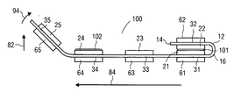
- FIG. 1illustrates a device 100 to be packaged in accordance with the present invention.
- device 100is a semiconductor device that includes a plurality of device dies or chips encapsulated on a tape substrate 12 .
- FIG. 1shows five device units formed on a front side 14 of tape substrate 12 , each unit may include one or more dies encapsulated therein.
- device 100includes device units 21 , 22 , 23 , 24 , and 25 , which are also referred to as capsules, formed in sections 31 , 32 , 33 , 34 , and 35 , respectively, of tape substrate 12 .
- the sections in tape substrate 12are also referred to as segments.
- the minimum distance between two adjacent device units on tape substrate 12depends on the thickness and flexibility of tape substrate 12 as well as the thickness of the device units.
- FIG. 1shows that the distance between device units 23 and 24 is greater than those between device units 21 and 22 and between device units 24 and 25 , but less than that between device units 21 and 23 .
- This specific distance arrangementis used for packaging, in which device units 21 - 25 are stacked together in a specific order described herein after with reference to FIGS. 6A-6H.
- the arrangement of the minimum distances between adjacent device unitsalso change accordingly.
- the distances between adjacent device unitsare uniform throughout tape substrate 12 at a value sufficient for stacking device units 21 - 25 in various orders.
- each of device units 21 - 25has a thickness of approximately 0.2 millimeter (mm) and tape substrate 12 is about 0.1 mm thick.
- the minimum distance between device units 21 and 22 and between device units 24 and 25is approximately 0.9 mm.
- the minimum distance between device unit 23 and 24is approximately 1.5 mm, and the minimum distance between device units 21 and 23 is approximately 2.1 mm.
- the electronics circuits in device units 21 - 25communicate with each other through conductive paths formed in tape substrate 12 between front side 14 and a back side 16 .
- Ball grid arrays(not shown) may be formed on back side 16 , thereby enabling the communication between device 100 with other devices and circuits.
- the location of the ball grid arraysdepends on the order in which device units 21 - 25 are stacked together.
- one ball grid arrayis formed on back side 16 of tape substrate 12 in section 31 .
- two ball arraysare formed on back side 16 of tape substrate 12 , one in section 31 and another in section 33 .
- Encapsulating dies on tape substrate 12 to form device units 21 - 25may include such procedures as molding, encapsulating, and sealing, which are known in the art. Prior to encapsulation, molding, or sealing, other processes such as, for example, wire bonding, lead bonding, bump bonding, and die stacking may be performed upon device units 21 - 25 prior to encapsulation. After encapsulation, molding, or sealing, device units 21 - 25 may be subject to additional processes such as ball attaching, marking, etc.
- device units 21 - 25are not limited to being formed using those procedures described herein above. It should also be noted that device 100 is not limited to having five device units formed thereon. In accordance with the present invention, device 100 may include any number of device units formed on tape substrate 12 . Furthermore, device 100 is not limited to having device units formed on front side 14 of tape substrate 12 . A device packaging apparatus and a packaging process in accordance with the present invention are also capable of packaging a device with device units formed on both front side 14 and back side 16 of tape substrate 12 .
- FIG. 2is a diagram illustrating one embodiment of a device packaging apparatus 200 for performing a multiple chip packaging process in accordance with the present invention.
- Apparatus 200includes a plurality of robotic arms 51 and 52 .
- a plurality of clamping elements 61 and 62are attached to respective robotic arms 51 and 52 .
- clamping elements 61 and 62include vacuum chucks.
- Apparatus 200further includes an adhesive applicator 67 .
- adhesive applicator 67applies an adhesive tape or film during the packaging process.
- adhesive applicator 67applies a fluid adhesive, e.g., epoxy.
- control module 68is coupled to robotic arms 51 and 52 , clamping elements 61 and 62 , and adhesive applicator 67 .
- control module 68includes a microprocessor (MP) or a central processing unit (CPU).
- Control module 68is also coupled to a memory 69 , which stores program routines for the operation of apparatus 200 .
- FIG. 2shows apparatus 200 as having two robotic arms 51 and 52 , two clamping elements 61 and 62 , and one adhesive applicator 67 , this is not intended as a limitation on the scope of the present invention.
- apparatus 200may include any plural number of robotic arms and clamping elements.
- Apparatus 200may also include more than one adhesive applicator.
- apparatus 200includes several adhesive applicators for applying different types of adhesives.
- apparatus 200may include other elements not shown in FIG. 2.
- apparatus 200includes a heating element.
- apparatus 200includes a cooling element.
- apparatus 200includes a source of electromagnetic radiation, e.g., infrared radiation, microwave radiation, etc.
- Apparatus 200may also include a combination of the above mentioned elements. Different variations of the packaging process in accordance with alternative embodiments of the present invention determine what elements that apparatus 200 includes.
- control module 68executes the program routines stored in memory 69 and controls robotic arms 51 and 52 , clamping elements 61 and 62 , and adhesive applicator 67 to package a multiple die device such as device 100 shown in FIG. 1.
- the mechanism for operating robotic arms 51 and 52 , clamping elements 61 and 62 , and adhesive applicator 67may include robotic, electromechanical, electromagnetic, pneumatic, hydraulic, etc.
- robotic arms 51 and 52can move and rotate independently of each other, thereby enabling apparatus 200 to precisely package devices of various characters.
- Apparatus 200is capable of packaging multiple die devices of various characters.
- control module 68instructs robotic arms 51 - 55 , clamping elements 61 - 65 , and adhesive applicator 67 to perform the packaging process.
- the program routinescan be modified to accommodate devices of different characters, which include tape substrate thickness and flexibility, device unit thickness and dimension, the number and locations of the device units on the tape substrate, etc.
- the program routinescan also be modified to apply different adhesives and use different elements to cure the adhesives.
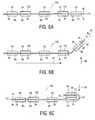
- FIGS. 3A-3Dillustrates a device packaging process in accordance with an embodiment of the present invention.
- the processuses a device packaging apparatus like apparatus 200 shown in FIG. 2 to package a device 100 having two device units 21 and 22 formed on front side 14 of tape substrate 12 .
- device units 21 and 22are formed in segments 31 and 32 , respectively, of tape substrate 12 .
- segments 31 and 32 of tape substrate 12are secured to clamping elements 61 and 62 , respectively, of apparatus 200 .
- clamping elements 61 and 62are vacuum chucks.
- Device 100is secured to clamping elements 61 and 62 by placing back side 16 of tape substrate 12 in segments 31 and 32 over the vacuum chucks and turning on vacuum chucks 61 and 62 .
- an adhesive 101is applied on device unit 21 using adhesive applicator 67 of FIG. 2.
- Adhesive 101can be a paste or fluid adhesive such as epoxy; it can also be an adhesive tape or film. It should be noted that adhesive 101 is not limited to being applied on device unit 21 . In accordance with an embodiment of the present invention, adhesive can be applied on device unit 21 , device unit 22 , or both. Further, adhesive 101 is not limited to being applied to completely cover the whole top surface of device unit 21 .
- clamping element 61moves in a first direction toward clamping element 62 as indicated by an arrow 81 .
- Clamping element 62moves in a second direction, as indicated by an arrow 82 , substantially perpendicular to first direction 81 .
- clamping element 62rotates in a direction indicated by an arrow 92 to bend or fold tape substrate 12 .
- clamping element 62rotates over an angle of approximately 180 degrees (°) to place device unit 22 substantially facing device unit 21 .
- the motion of clamping element 61 in first direction 81 toward clamping element 62is optional in a packaging process in accordance with the present invention.
- clamping element 61does not move, and clamping element 62 rotates and moves toward clamping element 61 , thereby avoiding over stretching tape substrate 12 .
- clamping element 62moves in a third direction, as indicated by an arrow 83 , substantially perpendicular to second direction 82 shown in FIG. 3C to place device unit 22 in substantial contact with device unit 21 .
- device unit 22is in good contact with adhesive 101 applied on device unit 21 . This can be achieved by applying a force on device 100 through clamping elements 61 and 62 to press device units 21 and 22 against each other.
- Curing adhesive 101may be as simple as holding device units 21 and 22 in place by clamping elements 61 and 62 for a period long enough for adhesive 101 to be cured.
- the curing periodgenerally depends on the characteristics of adhesive 101 and curing conditions.
- the curing conditionmay be changed up by altering the environment surrounding device 100 .
- the curing conditioncan be changed by taking such actions as heating device units 21 and 22 , cooling device units 21 and 22 , irradiating device units 21 and 22 with an electromagnetic radiation, e.g., infrared radiation, microwave radiation, etc., or any combination thereof. What actual actions to take depends on the characteristics of adhesive 101 .
- clamping elements 61 and 62are detached or released from respective segments 31 and 32 of tape substrate 12 .
- the packagingis completed.
- FIG. 4shows a semiconductor device 100 after being packaged in accordance with an embodiment of the present invention.
- Device 400 shown in FIG. 4has three capsules or device units formed on front side 14 of tape substrate 12 .
- the packaging of device 100 shown in FIG. 4is similar to that described herein above with reference to FIGS. 3A-3D.
- sections 31 , 32 , and 33on which respective device units 21 , 22 , and 23 are formed, are secured to three clamping elements, e.g., clamping elements 61 , 62 , and 63 of apparatus 200 shown in FIG. 2.
- Adhesive 101is applied on device unit 21 , device unit 22 , or both.
- the clamping element which secures section 32 of tape substrate 12rotates and moves to place device unit 22 facing and in substantial contact with device unit 21 .
- the clamping elementis then released from section 32 of tape substrate 12 .
- the adhesive 101is cured before releasing the clamping element from section 32 of tape substrate 12 .
- an adhesive 102is applied on device unit 23 , back side 16 of tape substrate 12 in section 32 , or both.
- Adhesive 102can be of the same type as or different from adhesive 101 .
- the clamping element securing section 33 of tape substrate 12moves and rotates for approximately 180° to place device unit 23 facing and in contact with section 32 of tape substrate 12 .
- adhesive 102is cured before releasing the clamping elements from sections 31 and 33 of tape substrate 12 .
- the curing of adhesives 101 and 102may include heating device, cooling device, irradiating device with a radiation, or any combination thereof.
- Adhesives 101 and 102may be cured at different times or all at once after device units 21 , 22 , and 23 are stacked together.
- FIG. 5shows another device 100 after being packaged in accordance with an embodiment of the present invention.
- Device 500 shown in FIG. 5has four capsules or device units formed on front side 14 of tape substrate 12 .
- FIG. 4shows that section 32 is on one side of section 31 and section 33 is on the other side of section 31 of tape substrate 12 . Further, section 34 is adjacent section 33 and on the opposite side of section 33 from section 31 .
- the packaging of device 100 shown in FIG. 5is similar to those described herein above with reference to FIGS. 3A-3D and FIG. 4.
- sections 31 , 32 , 33 , and 34on which respective device units 21 , 22 , 23 , and 24 are formed, are secured to three clamping elements, e.g., clamping elements 61 , 62 , 63 , and 64 of apparatus 200 shown in FIG. 2.
- An adhesive 101is applied on at least one of device unit 21 and device unit 22 .
- the clamping element securing section 32 of tape substrate 12rotates and moves to place device unit 22 facing and in substantial contact with device unit 21 .
- An adhesive 102is applied on at least one of device unit 23 and device unit 24 .
- the clamping element securing section 34 of tape substrate 12rotates and moves to place device unit 24 facing and in substantial contact with device unit 23 .
- the clamping elementsare then released from sections 32 and 34 of tape substrate 12 .
- the adhesives 101 and 102may be cured before releasing the clamping elements from sections 32 and 34 of tape substrate 12 .
- An adhesive 103is applied on back side 16 of tape substrate 12 in at least one of sections 32 and 34 .
- the clamping element securing section 33 of tape substrate 12moves and rotates for approximately 180° to place section 34 facing and in contact with section 32 of tape substrate 12 .
- the adhesive 103is cured before releasing the clamping elements from sections 31 and 33 of tape substrate 12 .
- the curing of adhesives 101 , 102 , and 103may include heating device, cooling device, irradiating device with an electromagnetic radiation, or any combination thereof.
- Adhesives 101 , 102 , and 103may be cured at different times or all at once after device units 21 , 22 , 23 , and 24 are stacked together.
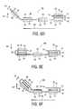
- FIGS. 6A-6Hillustrate a device packaging process in accordance with another embodiment of the present invention.
- the processuses a device packaging apparatus like apparatus 200 shown in FIG. 2 to packaging a device 100 having five device units 21 , 22 , 23 , 24 , and 25 formed on front side 14 of tape substrate 12 .
- device units 21 , 22 , 23 , 24 , and 25are formed in segments 31 , 32 , 33 , 34 , and 35 , respectively, of tape substrate 12 .
- FIG. 6Ashows that segment 32 is on one side of segment 31 and segments 33 , 34 , and 35 are on the other side of segment 31 .
- segment 33is located between segments 31 and 34
- segment 34is located between segments 33 and 35 .
- the packing of device 100 with device units 21 - 25is similar to those described herein above with reference to FIGS. 3A-3D, FIG. 4, and FIG. 5.
- segments 31 , 32 , 33 , 34 , and 35 of tape substrate 12are secured to clamping elements 61 , 62 , 63 , 64 , and 65 , respectively, of apparatus 200 .
- clamping elements 61 - 65are vacuum chucks.
- Device 100is secured to clamping elements 61 - 65 by placing back side 16 of tape substrate 12 in segments 31 - 35 on the vacuum chucks and turning on vacuum chucks 61 - 65 .
- An adhesive 101is applied on device unit 21 , device unit 22 , or both.
- An adhesive 102is applied on at least one of device unit 24 and device unit 25 .
- clamping elements 61 , 63 , 64 , and 65move in a first direction toward clamping element 62 as indicated by an arrow 81 in FIG. 6B.
- Clamping element 62moves in a second direction, as indicated by an arrow 82 in FIG. 6B, substantially perpendicular to first direction 81 .
- clamping element 62rotates in a direction indicated by an arrow 92 in FIG. 6B for approximately 180° to bend or fold tape substrate 12 and to place device unit 22 substantially facing device unit 21 .
- clamping element 62moves in a third direction, as indicated by an arrow 83 , substantially opposite to second direction 82 shown in FIG. 6B to place device unit 22 in substantial contact with device unit 21 .
- Device unit 22is in good contact with adhesive 101 applied on device unit 21 . This can be achieved by asserting a force on device 100 through clamping elements 61 and 62 to press device units 21 and 22 against each other. After clamping elements 61 and 62 stack device units 21 and 22 together, adhesive 101 is cured. Curing adhesive 101 may include any procedures describe herein above with reference to FIGS. 3A-3D. After curing adhesive 101 , clamping element 62 is released from back side 16 of tape substrate 12 .
- Clamping elements 61 , 63 , and 64move in a fourth direction toward clamping element 65 as indicated by an arrow 84 in FIG. 6D.
- Clamping element 65moves in second direction 82 and rotates in a direction indicated by an arrow 94 in FIG. 6D for approximately 180° to bend or fold tape substrate 12 and to place device unit 25 substantially facing device unit 24 .
- clamping element 65moves in third direction 83 to place device unit 25 in substantial contact with device unit 24 .
- Adhesive 102is cured and clamping element 65 is subsequently released from back side 16 of tape substrate 12 .
- an adhesive 103is applied on at least one of device unit 23 and back side 16 of tape substrate 12 in segment 35 .
- Clamping elements 61 and 63move in fourth direction 84 toward clamping element 64 .
- Clamping element 64moves in second direction 82 and rotates in direction 94 for approximately 180° to fold tape substrate 12 and to place segment 35 of tape substrate 12 substantially facing device unit 23 .
- clamping element 64moves in third direction 83 to place segment 35 of tape substrate 12 in substantial contact with device unit 23 . Clamping element 64 is released from back side 16 of tape substrate 12 after curing adhesive 103 .
- an adhesive 104is applied on back side 16 of tape substrate 12 in at least one of segments 32 and 34 .
- Clamping elements 61moves in fourth direction 84 toward clamping element 63 .
- Clamping element 63moves in second direction 82 and rotates in direction 94 for approximately 180° to fold tape substrate 12 and to place segment 34 of tape substrate 12 substantially facing segment 32 of tape substrate 12 .
- clamping element 63moves in third direction 83 to place segment 34 of tape substrate 12 in substantial contact with segment 32 of tape substrate 12 .
- Adhesive 104is cured. Clamping elements 61 and 63 are subsequently released from back side 16 of tape substrate 12 .
- FIGS. 7A-7Billustrate a device packaging process in accordance with yet another embodiment of the present invention.
- the processuses a device packaging apparatus like apparatus 200 shown in FIG. 2 to packaging a device 100 having a single device unit 21 formed on front side 14 of tape substrate 12 .
- device unit 21is formed in segment 31 of tape substrate 12 .
- segment 32 of tape substrate 12There is no device unit formed in segment 32 of tape substrate 12 , which is adjacent to segment 31 of tape substrate 12 .
- Adhesive 101can be a paste or fluid adhesive such as epoxy; it can also be an adhesive tape or film. It should be noted that adhesive 101 is not limited to being applied on device unit 21 . In accordance with an embodiment of the present invention, adhesive can be applied on device unit 21 , front side 14 of tape substrate 12 in segment 32 , or both.
- clamping elements 61 and 62moves and rotates to fold tape substrate 12 and stack segment 32 of tape substrate 12 over device unit 21 .
- front side 14 of tape substrate 12 in segment 32is in good contact with adhesive 101 applied on device unit 21 . This can be achieved by applying a force on device 100 through clamping elements 61 and 62 to press segment 32 of tape substrate 12 against device units 21 .
- Adhesive 101is cured. After curing adhesive 101 , clamping elements 61 and 62 are detached or released from respective segments 31 and 32 of tape substrate 12 .
- the movements the clamping elements in first direction 81 and fourth direction 84 as described herein above with reference to FIGS. 3A-3D and 6 A- 6 Havoid over stretching tape substrate 12 .
- the over stretch of tape substrate 12can also be avoided by moving the clamping element that is in rotation toward the rest of the clamping elements secured to the remaining segments of tape substrate 12 .
- a packaging apparatusin accordance with one embodiment of the present invention includes a plurality of robotic arms and a plurality of clamping elements attached to the robotic arms for clamping different segments of the tape substrate and folding the tape substrate, thereby stacking the device units together.
- the packaging apparatusalso includes an element for applying adhesives on the device units and the tape substrate.
- the packaging apparatusmay include elements for facilitating the curing of the adhesive.
- the packaging process and the apparatus of one embodiment of the present inventioncan be easily adapted for packaging devices with various characters and dimensions.
- the apparatusis capable of integrally performing different steps of the package process and handling the device with high precision.
- the device packaging process and the apparatusare applicable in various areas of semiconductor device manufacturing processes, such as, for example, chip scale packaging, memory device packaging, communication device packaging, etc.
- the packaging process and apparatus of one embodiment of the present inventioncan package devices with any plural number of device units formed on a tape substrate. Further, the packaging process and apparatus of one embodiment of the present invention can also package devices with device units formed on both sides of the tape substrate.
- the application of the packaging process in accordance with alternative embodiments of the present inventionis not limited to semiconductor device manufacturing. The packaging process and apparatus of alternative embodiments of the present invention can be used in any area that benefits from packaging at one or more units into a package.
Landscapes
- Engineering & Computer Science (AREA)
- Microelectronics & Electronic Packaging (AREA)
- Power Engineering (AREA)
- Physics & Mathematics (AREA)
- Condensed Matter Physics & Semiconductors (AREA)
- General Physics & Mathematics (AREA)
- Computer Hardware Design (AREA)
- Manufacturing & Machinery (AREA)
- Encapsulation Of And Coatings For Semiconductor Or Solid State Devices (AREA)
Abstract
Description
- Embodiments of the present invention relate, in general, to device manufacturing and packaging and, more particularly, to the packaging of a device with multiple units formed on a tape substrate.[0001]
- Device packaging is an important part of semiconductor device manufacturing processes. A process for packaging multiple device dies into a single device package includes bonding the device dies on a tape substrate and packaging the dies and the tape substrate into a single device. One such packaging process includes folding the tape substrate to stack the multiple device dies bonded thereon together. The adhesives dispensed between the dies in the stack are cured, thereby holding the dies in the stack together.[0002]
- An apparatus used for such a tape substrate packaging process typically has mechanical fingers and pusher to handle the dies and the tape substrate. Specifically, the mechanical fingers and pushers stack the dies together. Another apparatus design may include a hinged assembly to fold the tape substrate. Currently, the adhesive dispensing is generally performed manually or by equipment separate from the device packaging apparatus.[0003]
- The mechanical fingers and pusher, or hinged assembly in an existing packaging apparatus are generally deficient in ensuring accurate positions of the dies and tape substrate during the packaging process. In addition, the apparatus generally does not integrate adhesive dispensing and curing into the device packaging process. The apparatus is not easily modifiable for packaging different devices. The tape substrate device packaging processes using the existing apparatuses are generally time consuming.[0004]
- The accompanying drawings, which are incorporated in and form a part of this specification, illustrate embodiments of the present invention and, together with the description, serve to explain the principles of the present invention:[0005]
- FIG. 1 illustrates one embodiment of a device to be packaged in accordance with the present invention;[0006]
- FIG. 2 is a functional block diagram illustrating one embodiment of an apparatus for performing a packaging process in accordance with the present invention;[0007]
- FIGS. 3A-3D illustrates one embodiment of a device packaging process in accordance with an aspect of the present invention;[0008]
- FIG. 4 illustrates one embodiment of a semiconductor device after being packaged in accordance with the present invention;[0009]
- FIG. 5 illustrates an alternative embodiment of another semiconductor device after being packaged in accordance with the present invention;[0010]
- FIGS. 6A-6H illustrates one embodiment of a device packaging process in accordance with another aspect of the present invention; and[0011]
- FIGS. 7A-7B illustrates one embodiment of a device packaging process in accordance with yet another aspect of the present invention.[0012]
- Reference will now be made to the several embodiments of the invention, examples of which are illustrated in the accompanying drawings. While the present invention will be described in conjunction with the different embodiments, it will be understood that they are not intended to limit the invention to these embodiments. On the contrary, the present invention is intended to cover alternatives, modifications and equivalents, which may be included within the spirit and scope of the invention as defined by the claims. Moreover, in the following detailed description of the present invention, numerous specific details are set forth in order to provide a thorough understanding of the present invention. However, the present invention may be practiced without these specific details. In other instances, well-known methods, procedures, components and circuits have not been described in detail as not to unnecessarily obscure aspects of the present invention.[0013]
- FIG. 1 illustrates a[0014]
device 100 to be packaged in accordance with the present invention. By way of example,device 100 is a semiconductor device that includes a plurality of device dies or chips encapsulated on atape substrate 12. FIG. 1 shows five device units formed on afront side 14 oftape substrate 12, each unit may include one or more dies encapsulated therein. Specifically,device 100 includesdevice units sections tape substrate 12. The sections intape substrate 12 are also referred to as segments. - The minimum distance between two adjacent device units on[0015]
tape substrate 12 depends on the thickness and flexibility oftape substrate 12 as well as the thickness of the device units. By way of example, FIG. 1 shows that the distance betweendevice units device units device units device units tape substrate 12 at a value sufficient for stacking device units21-25 in various orders. - In one example, each of device units[0016]21-25 has a thickness of approximately 0.2 millimeter (mm) and
tape substrate 12 is about 0.1 mm thick. In such an example, the minimum distance betweendevice units device units device unit device units - The electronics circuits in device units[0017]21-25 communicate with each other through conductive paths formed in
tape substrate 12 betweenfront side 14 and aback side 16. Ball grid arrays (not shown) may be formed onback side 16, thereby enabling the communication betweendevice 100 with other devices and circuits. The location of the ball grid arrays depends on the order in which device units21-25 are stacked together. In accordance with one embodiment, one ball grid array is formed onback side 16 oftape substrate 12 insection 31. In another embodiment, two ball arrays are formed onback side 16 oftape substrate 12, one insection 31 and another insection 33. - Encapsulating dies on[0018]
tape substrate 12 to form device units21-25 may include such procedures as molding, encapsulating, and sealing, which are known in the art. Prior to encapsulation, molding, or sealing, other processes such as, for example, wire bonding, lead bonding, bump bonding, and die stacking may be performed upon device units21-25 prior to encapsulation. After encapsulation, molding, or sealing, device units21-25 may be subject to additional processes such as ball attaching, marking, etc. - It should be noted that, in accordance with an embodiment of the present invention, device units[0019]21-25 are not limited to being formed using those procedures described herein above. It should also be noted that
device 100 is not limited to having five device units formed thereon. In accordance with the present invention,device 100 may include any number of device units formed ontape substrate 12. Furthermore,device 100 is not limited to having device units formed onfront side 14 oftape substrate 12. A device packaging apparatus and a packaging process in accordance with the present invention are also capable of packaging a device with device units formed on bothfront side 14 andback side 16 oftape substrate 12. - FIG. 2 is a diagram illustrating one embodiment of a[0020]
device packaging apparatus 200 for performing a multiple chip packaging process in accordance with the present invention.Apparatus 200 includes a plurality ofrobotic arms clamping elements robotic arms clamping elements Apparatus 200 further includes anadhesive applicator 67. In one embodiment,adhesive applicator 67 applies an adhesive tape or film during the packaging process. In another embodiment,adhesive applicator 67 applies a fluid adhesive, e.g., epoxy. Acontrol module 68 is coupled torobotic arms elements adhesive applicator 67. By way of example,control module 68 includes a microprocessor (MP) or a central processing unit (CPU).Control module 68 is also coupled to amemory 69, which stores program routines for the operation ofapparatus 200. - Although FIG. 2[0021]
shows apparatus 200 as having tworobotic arms elements adhesive applicator 67, this is not intended as a limitation on the scope of the present invention. Depending on the characters of the devices to be packaged,apparatus 200 may include any plural number of robotic arms and clamping elements.Apparatus 200 may also include more than one adhesive applicator. In an alternative embodiment,apparatus 200 includes several adhesive applicators for applying different types of adhesives. Furthermore,apparatus 200 may include other elements not shown in FIG. 2. In one embodiment,apparatus 200 includes a heating element. In anotherembodiment apparatus 200 includes a cooling element. In yet another embodiment,apparatus 200 includes a source of electromagnetic radiation, e.g., infrared radiation, microwave radiation, etc.Apparatus 200 may also include a combination of the above mentioned elements. Different variations of the packaging process in accordance with alternative embodiments of the present invention determine what elements thatapparatus 200 includes. - In operation,[0022]
control module 68 executes the program routines stored inmemory 69 and controlsrobotic arms elements adhesive applicator 67 to package a multiple die device such asdevice 100 shown in FIG. 1. The mechanism for operatingrobotic arms elements adhesive applicator 67 may include robotic, electromechanical, electromagnetic, pneumatic, hydraulic, etc. In one embodiment,robotic arms apparatus 200 to precisely package devices of various characters. - [0023]
Apparatus 200 is capable of packaging multiple die devices of various characters. By executing the program routines stored inmemory 69,control module 68 instructs robotic arms51-55, clamping elements61-65, andadhesive applicator 67 to perform the packaging process. The program routines can be modified to accommodate devices of different characters, which include tape substrate thickness and flexibility, device unit thickness and dimension, the number and locations of the device units on the tape substrate, etc. The program routines can also be modified to apply different adhesives and use different elements to cure the adhesives. - FIGS. 3A-3D illustrates a device packaging process in accordance with an embodiment of the present invention. The process uses a device packaging apparatus like[0024]
apparatus 200 shown in FIG. 2 to package adevice 100 having twodevice units front side 14 oftape substrate 12. Specifically,device units segments tape substrate 12. - As shown in FIG. 3A,[0025]
segments tape substrate 12 are secured to clampingelements apparatus 200. In one embodiment, clampingelements Device 100 is secured to clampingelements side 16 oftape substrate 12 insegments - In a next step, as shown in FIG. 3B, an adhesive[0026]101 is applied on
device unit 21 usingadhesive applicator 67 of FIG. 2. Adhesive101 can be a paste or fluid adhesive such as epoxy; it can also be an adhesive tape or film. It should be noted that adhesive101 is not limited to being applied ondevice unit 21. In accordance with an embodiment of the present invention, adhesive can be applied ondevice unit 21,device unit 22, or both. Further, adhesive101 is not limited to being applied to completely cover the whole top surface ofdevice unit 21. - In FIG. 3C, clamping[0027]
element 61 moves in a first direction toward clampingelement 62 as indicated by anarrow 81. Clampingelement 62 moves in a second direction, as indicated by anarrow 82, substantially perpendicular tofirst direction 81. In addition, clampingelement 62 rotates in a direction indicated by anarrow 92 to bend or foldtape substrate 12. In accordance with an embodiment of the present invention, clampingelement 62 rotates over an angle of approximately 180 degrees (°) to placedevice unit 22 substantially facingdevice unit 21. It should be noted that the motion of clampingelement 61 infirst direction 81 toward clampingelement 62 is optional in a packaging process in accordance with the present invention. In an alternative embodiment, clampingelement 61 does not move, and clampingelement 62 rotates and moves toward clampingelement 61, thereby avoiding over stretchingtape substrate 12. - In FIG. 3D, clamping[0028]
element 62 moves in a third direction, as indicated by anarrow 83, substantially perpendicular tosecond direction 82 shown in FIG. 3C to placedevice unit 22 in substantial contact withdevice unit 21. In one embodiment,device unit 22 is in good contact with adhesive101 applied ondevice unit 21. This can be achieved by applying a force ondevice 100 through clampingelements device units - After clamping[0029]
elements stack device units device units elements environment surrounding device 100. For example, the curing condition can be changed by taking such actions asheating device units cooling device units device units adhesive 101. - After curing adhesive[0030]101, clamping
elements respective segments tape substrate 12. The packaging is completed. - FIG. 4 shows a[0031]
semiconductor device 100 after being packaged in accordance with an embodiment of the present invention.Device 400 shown in FIG. 4 has three capsules or device units formed onfront side 14 oftape substrate 12. The packaging ofdevice 100 shown in FIG. 4 is similar to that described herein above with reference to FIGS. 3A-3D. - First,[0032]
sections respective device units elements apparatus 200 shown in FIG. 2.Adhesive 101 is applied ondevice unit 21,device unit 22, or both. The clamping element which securessection 32 oftape substrate 12 rotates and moves to placedevice unit 22 facing and in substantial contact withdevice unit 21. The clamping element is then released fromsection 32 oftape substrate 12. In one embodiment, the adhesive101 is cured before releasing the clamping element fromsection 32 oftape substrate 12. - In a subsequent step, an adhesive[0033]102 is applied on
device unit 23, backside 16 oftape substrate 12 insection 32, or both. Adhesive102 can be of the same type as or different from adhesive101. The clampingelement securing section 33 oftape substrate 12 moves and rotates for approximately 180° to placedevice unit 23 facing and in contact withsection 32 oftape substrate 12. In one embodiment, adhesive102 is cured before releasing the clamping elements fromsections tape substrate 12. - Depending on their properties, the curing of[0034]
adhesives Adhesives device units - FIG. 5 shows another[0035]
device 100 after being packaged in accordance with an embodiment of the present invention.Device 500 shown in FIG. 5 has four capsules or device units formed onfront side 14 oftape substrate 12. FIG. 4 shows thatsection 32 is on one side ofsection 31 andsection 33 is on the other side ofsection 31 oftape substrate 12. Further,section 34 isadjacent section 33 and on the opposite side ofsection 33 fromsection 31. The packaging ofdevice 100 shown in FIG. 5 is similar to those described herein above with reference to FIGS. 3A-3D and FIG. 4. - First,[0036]
sections respective device units elements apparatus 200 shown in FIG. 2. An adhesive101 is applied on at least one ofdevice unit 21 anddevice unit 22. The clampingelement securing section 32 oftape substrate 12 rotates and moves to placedevice unit 22 facing and in substantial contact withdevice unit 21. An adhesive102 is applied on at least one ofdevice unit 23 anddevice unit 24. The clampingelement securing section 34 oftape substrate 12 rotates and moves to placedevice unit 24 facing and in substantial contact withdevice unit 23. The clamping elements are then released fromsections tape substrate 12. In one embodiment, theadhesives sections tape substrate 12. - An adhesive[0037]103 is applied on
back side 16 oftape substrate 12 in at least one ofsections element securing section 33 oftape substrate 12 moves and rotates for approximately 180° to placesection 34 facing and in contact withsection 32 oftape substrate 12. In one embodiment, the adhesive103 is cured before releasing the clamping elements fromsections tape substrate 12. - Depending on their properties, the curing of[0038]
adhesives Adhesives device units - FIGS. 6A-6H illustrate a device packaging process in accordance with another embodiment of the present invention. The process uses a device packaging apparatus like[0039]
apparatus 200 shown in FIG. 2 to packaging adevice 100 having fivedevice units front side 14 oftape substrate 12. Specifically,device units segments tape substrate 12. FIG. 6A shows thatsegment 32 is on one side ofsegment 31 andsegments segment 31. Furthermore,segment 33 is located betweensegments segment 34 is located betweensegments device 100 with device units21-25 is similar to those described herein above with reference to FIGS. 3A-3D, FIG. 4, and FIG. 5. - As shown in FIG. 6A,[0040]
segments tape substrate 12 are secured to clampingelements apparatus 200. In one embodiment, clamping elements61-65 are vacuum chucks.Device 100 is secured to clamping elements61-65 by placing backside 16 oftape substrate 12 in segments31-35 on the vacuum chucks and turning on vacuum chucks61-65. An adhesive101 is applied ondevice unit 21,device unit 22, or both. An adhesive102 is applied on at least one ofdevice unit 24 anddevice unit 25. - In a subsequent step, clamping[0041]
elements element 62 as indicated by anarrow 81 in FIG. 6B. Clampingelement 62 moves in a second direction, as indicated by anarrow 82 in FIG. 6B, substantially perpendicular tofirst direction 81. In addition, clampingelement 62 rotates in a direction indicated by anarrow 92 in FIG. 6B for approximately 180° to bend or foldtape substrate 12 and to placedevice unit 22 substantially facingdevice unit 21. - In FIG. 6C, clamping[0042]
element 62 moves in a third direction, as indicated by anarrow 83, substantially opposite tosecond direction 82 shown in FIG. 6B to placedevice unit 22 in substantial contact withdevice unit 21.Device unit 22 is in good contact with adhesive101 applied ondevice unit 21. This can be achieved by asserting a force ondevice 100 through clampingelements device units elements stack device units element 62 is released from backside 16 oftape substrate 12. - Clamping[0043]
elements element 65 as indicated by anarrow 84 in FIG. 6D. Clampingelement 65 moves insecond direction 82 and rotates in a direction indicated by anarrow 94 in FIG. 6D for approximately 180° to bend or foldtape substrate 12 and to placedevice unit 25 substantially facingdevice unit 24. - In FIG. 6E, clamping[0044]
element 65 moves inthird direction 83 to placedevice unit 25 in substantial contact withdevice unit 24.Adhesive 102 is cured and clampingelement 65 is subsequently released from backside 16 oftape substrate 12. - Next as shown in FIG. 6F, an adhesive[0045]103 is applied on at least one of
device unit 23 and backside 16 oftape substrate 12 insegment 35. Clampingelements fourth direction 84 toward clampingelement 64. Clampingelement 64 moves insecond direction 82 and rotates indirection 94 for approximately 180° to foldtape substrate 12 and to placesegment 35 oftape substrate 12 substantially facingdevice unit 23. - In FIG. 6G, clamping[0046]
element 64 moves inthird direction 83 to placesegment 35 oftape substrate 12 in substantial contact withdevice unit 23. Clampingelement 64 is released from backside 16 oftape substrate 12 after curing adhesive103. - Next as shown in FIG. 6H, an adhesive[0047]104 is applied on
back side 16 oftape substrate 12 in at least one ofsegments elements 61 moves infourth direction 84 toward clampingelement 63. Clampingelement 63 moves insecond direction 82 and rotates indirection 94 for approximately 180° to foldtape substrate 12 and to placesegment 34 oftape substrate 12 substantially facingsegment 32 oftape substrate 12. Then, clampingelement 63 moves inthird direction 83 to placesegment 34 oftape substrate 12 in substantial contact withsegment 32 oftape substrate 12.Adhesive 104 is cured. Clampingelements side 16 oftape substrate 12. - FIGS. 7A-7B illustrate a device packaging process in accordance with yet another embodiment of the present invention. The process uses a device packaging apparatus like[0048]
apparatus 200 shown in FIG. 2 to packaging adevice 100 having asingle device unit 21 formed onfront side 14 oftape substrate 12. Specifically,device unit 21 is formed insegment 31 oftape substrate 12. There is no device unit formed insegment 32 oftape substrate 12, which is adjacent tosegment 31 oftape substrate 12. - First, as shown in FIG. 7A,[0049]
segments tape substrate 12 are secured to clampingelements device unit 21. Adhesive101 can be a paste or fluid adhesive such as epoxy; it can also be an adhesive tape or film. It should be noted that adhesive101 is not limited to being applied ondevice unit 21. In accordance with an embodiment of the present invention, adhesive can be applied ondevice unit 21,front side 14 oftape substrate 12 insegment 32, or both. - Next, as shown in FIG. 7B, at least one of clamping[0050]
elements tape substrate 12 andstack segment 32 oftape substrate 12 overdevice unit 21. In one embodiment,front side 14 oftape substrate 12 insegment 32 is in good contact with adhesive101 applied ondevice unit 21. This can be achieved by applying a force ondevice 100 through clampingelements segment 32 oftape substrate 12 againstdevice units 21.Adhesive 101 is cured. After curing adhesive101, clampingelements respective segments tape substrate 12. - The movements the clamping elements in[0051]
first direction 81 andfourth direction 84 as described herein above with reference to FIGS. 3A-3D and6A-6H avoid over stretchingtape substrate 12. However, it should be noted that they are optional in accordance with the present invention. The over stretch oftape substrate 12 can also be avoided by moving the clamping element that is in rotation toward the rest of the clamping elements secured to the remaining segments oftape substrate 12. - It should be appreciated that an apparatus and a process for packaging a device with multiple units have been provided. A packaging apparatus in accordance with one embodiment of the present invention includes a plurality of robotic arms and a plurality of clamping elements attached to the robotic arms for clamping different segments of the tape substrate and folding the tape substrate, thereby stacking the device units together. In one embodiment of the present invention, the packaging apparatus also includes an element for applying adhesives on the device units and the tape substrate. Further, the packaging apparatus may include elements for facilitating the curing of the adhesive. When packaging a device with many device units on a tape substrate, in one embodiment, the two ends of the tape substrate one folded toward the central portion of the tape substrate. In alternative embodiments, the process may start from the central portion of the tape substrate. The packaging process and the apparatus of one embodiment of the present invention can be easily adapted for packaging devices with various characters and dimensions. The apparatus is capable of integrally performing different steps of the package process and handling the device with high precision. The device packaging process and the apparatus are applicable in various areas of semiconductor device manufacturing processes, such as, for example, chip scale packaging, memory device packaging, communication device packaging, etc.[0052]
- While specific embodiments of the present invention have been described herein above, they are not intended as a limitation on the scope of the present invention. The present invention encompasses those modifications and variations of the described embodiments that are obvious to those skilled in the art. For example, although the specification describes the packaging processes for packaging devices with one, two, three, four, and five device units, these are not limitations on the present invention. The packaging process and apparatus of one embodiment of the present invention can package devices with any plural number of device units formed on a tape substrate. Further, the packaging process and apparatus of one embodiment of the present invention can also package devices with device units formed on both sides of the tape substrate. In addition, the application of the packaging process in accordance with alternative embodiments of the present invention is not limited to semiconductor device manufacturing. The packaging process and apparatus of alternative embodiments of the present invention can be used in any area that benefits from packaging at one or more units into a package.[0053]
Claims (23)
Priority Applications (2)
| Application Number | Priority Date | Filing Date | Title |
|---|---|---|---|
| US10/228,617US7503155B2 (en) | 2002-08-26 | 2002-08-26 | Method for packaging a tape substrate |
| US12/362,445US20090133247A1 (en) | 2002-08-26 | 2009-01-29 | Apparatus for packaging a tape substrate |
Applications Claiming Priority (1)
| Application Number | Priority Date | Filing Date | Title |
|---|---|---|---|
| US10/228,617US7503155B2 (en) | 2002-08-26 | 2002-08-26 | Method for packaging a tape substrate |
Related Child Applications (1)
| Application Number | Title | Priority Date | Filing Date |
|---|---|---|---|
| US12/362,445DivisionUS20090133247A1 (en) | 2002-08-26 | 2009-01-29 | Apparatus for packaging a tape substrate |
Publications (2)
| Publication Number | Publication Date |
|---|---|
| US20040209400A1true US20040209400A1 (en) | 2004-10-21 |
| US7503155B2 US7503155B2 (en) | 2009-03-17 |
Family
ID=33158315
Family Applications (2)
| Application Number | Title | Priority Date | Filing Date |
|---|---|---|---|
| US10/228,617Expired - LifetimeUS7503155B2 (en) | 2002-08-26 | 2002-08-26 | Method for packaging a tape substrate |
| US12/362,445AbandonedUS20090133247A1 (en) | 2002-08-26 | 2009-01-29 | Apparatus for packaging a tape substrate |
Family Applications After (1)
| Application Number | Title | Priority Date | Filing Date |
|---|---|---|---|
| US12/362,445AbandonedUS20090133247A1 (en) | 2002-08-26 | 2009-01-29 | Apparatus for packaging a tape substrate |
Country Status (1)
| Country | Link |
|---|---|
| US (2) | US7503155B2 (en) |
Cited By (10)
| Publication number | Priority date | Publication date | Assignee | Title |
|---|---|---|---|---|
| US20050136531A1 (en)* | 2003-12-17 | 2005-06-23 | Kimberly-Clark Worldwide, Inc. | Folded substrate with applied chemistry |
| US20050227410A1 (en)* | 2004-04-09 | 2005-10-13 | Tessera, Inc. | Manufacture of microelectronic fold packages |
| US20060243392A1 (en)* | 2002-09-30 | 2006-11-02 | Pieda Ruel B | Forming folded-stack packaged device using progressive folding tool |
| US20090309197A1 (en)* | 2008-06-11 | 2009-12-17 | Seng Guan Chow | Integrated circuit package system with internal stacking module |
| US20120190153A1 (en)* | 2011-01-21 | 2012-07-26 | Seiko Epson Corporation | Method for connecting substrate and method for manufacturing semiconductor device |
| CN104900611A (en)* | 2015-06-09 | 2015-09-09 | 中国科学院微电子研究所 | Three-dimensional packaging heat dissipation structure based on flexible substrate and preparation method thereof |
| CN105118827A (en)* | 2015-08-10 | 2015-12-02 | 成都锐华光电技术有限责任公司 | Three-dimensional chip stack packaging structure based on flexible substrate and packaging method |
| DE102015219190A1 (en)* | 2015-10-05 | 2017-04-06 | Fraunhofer-Gesellschaft zur Förderung der angewandten Forschung e.V. | Method for producing an electronic component and electronic component |
| US11296063B2 (en)* | 2018-11-20 | 2022-04-05 | Lumens Co., Ltd. | Flexible LED display with processor under a folded edge portion |
| US11533819B2 (en)* | 2015-10-16 | 2022-12-20 | Delta Electronics, Inc. | Method for manufacturing a stack structure |
Families Citing this family (11)
| Publication number | Priority date | Publication date | Assignee | Title |
|---|---|---|---|---|
| US7888185B2 (en)* | 2006-08-17 | 2011-02-15 | Micron Technology, Inc. | Semiconductor device assemblies and systems including at least one conductive pathway extending around a side of at least one semiconductor device |
| US20090166065A1 (en)* | 2008-01-02 | 2009-07-02 | Clayton James E | Thin multi-chip flex module |
| BR112013031652A2 (en)* | 2011-06-09 | 2019-09-24 | Univ Miami | treatment methods for retinal diseases |
| US8834182B2 (en) | 2012-10-17 | 2014-09-16 | Microelectronics Assembly Technologies | Pierced flexible circuit and compression joint |
| US9338895B2 (en)* | 2012-10-17 | 2016-05-10 | Microelectronics Assembly Technologies | Method for making an electrical circuit |
| US8837141B2 (en) | 2012-10-17 | 2014-09-16 | Microelectronics Assembly Technologies | Electronic module with heat spreading enclosure |
| US8899994B2 (en) | 2012-10-17 | 2014-12-02 | Microelectronics Assembly Technologies, Inc. | Compression connector system |
| US8902606B2 (en) | 2012-10-17 | 2014-12-02 | Microelectronics Assembly Technologies | Electronic interconnect system |
| US8817458B2 (en) | 2012-10-17 | 2014-08-26 | Microelectronics Assembly Technologies, Inc. | Flexible circuit board and connection system |
| TWI562326B (en)* | 2015-05-22 | 2016-12-11 | Chipmos Technologies Inc | Stacked chip on film package structure and manufacturing method thereof |
| CN106409702A (en)* | 2016-11-22 | 2017-02-15 | 中国科学院微电子研究所 | Multi-chip stacking packaging structure and manufacturing method thereof |
Citations (5)
| Publication number | Priority date | Publication date | Assignee | Title |
|---|---|---|---|---|
| US4601689A (en)* | 1984-03-12 | 1986-07-22 | Unmanned Solutions, Inc. | Method and apparatus for folding polymeric sheet material and flexible disk jackets made thereby |
| US5776797A (en)* | 1995-12-22 | 1998-07-07 | Fairchild Space And Defense Corporation | Three-dimensional flexible assembly of integrated circuits |
| US6121676A (en)* | 1996-12-13 | 2000-09-19 | Tessera, Inc. | Stacked microelectronic assembly and method therefor |
| US6225688B1 (en)* | 1997-12-11 | 2001-05-01 | Tessera, Inc. | Stacked microelectronic assembly and method therefor |
| US7033911B2 (en)* | 2004-03-31 | 2006-04-25 | Intel Corporation | Adhesive of folded package |
Family Cites Families (2)
| Publication number | Priority date | Publication date | Assignee | Title |
|---|---|---|---|---|
| US5395198A (en)* | 1992-06-19 | 1995-03-07 | International Business Machines Corporation | Vacuum loading chuck and fixture for flexible printed circuit panels |
| US5553442A (en)* | 1994-10-06 | 1996-09-10 | James River Paper Company, Inc. | Robotic system for mixing articles in containers |
- 2002
- 2002-08-26USUS10/228,617patent/US7503155B2/ennot_activeExpired - Lifetime
- 2009
- 2009-01-29USUS12/362,445patent/US20090133247A1/ennot_activeAbandoned
Patent Citations (5)
| Publication number | Priority date | Publication date | Assignee | Title |
|---|---|---|---|---|
| US4601689A (en)* | 1984-03-12 | 1986-07-22 | Unmanned Solutions, Inc. | Method and apparatus for folding polymeric sheet material and flexible disk jackets made thereby |
| US5776797A (en)* | 1995-12-22 | 1998-07-07 | Fairchild Space And Defense Corporation | Three-dimensional flexible assembly of integrated circuits |
| US6121676A (en)* | 1996-12-13 | 2000-09-19 | Tessera, Inc. | Stacked microelectronic assembly and method therefor |
| US6225688B1 (en)* | 1997-12-11 | 2001-05-01 | Tessera, Inc. | Stacked microelectronic assembly and method therefor |
| US7033911B2 (en)* | 2004-03-31 | 2006-04-25 | Intel Corporation | Adhesive of folded package |
Cited By (18)
| Publication number | Priority date | Publication date | Assignee | Title |
|---|---|---|---|---|
| US20060243392A1 (en)* | 2002-09-30 | 2006-11-02 | Pieda Ruel B | Forming folded-stack packaged device using progressive folding tool |
| US20060243376A1 (en)* | 2002-09-30 | 2006-11-02 | Pieda Ruel B | Forming folded-stack packaged device using progressive folding tool |
| US20060243374A1 (en)* | 2002-09-30 | 2006-11-02 | Pieda Ruel B | Forming folded-stack packaged device using progressive folding tool |
| US20050136531A1 (en)* | 2003-12-17 | 2005-06-23 | Kimberly-Clark Worldwide, Inc. | Folded substrate with applied chemistry |
| US20050227410A1 (en)* | 2004-04-09 | 2005-10-13 | Tessera, Inc. | Manufacture of microelectronic fold packages |
| US7157309B2 (en)* | 2004-04-09 | 2007-01-02 | Tessera, Inc. | Manufacture of microelectronic fold packages |
| US9030006B2 (en) | 2008-06-09 | 2015-05-12 | Stats Chippac Ltd. | Integrated circuit package system with internal stacking module |
| US8278141B2 (en)* | 2008-06-11 | 2012-10-02 | Stats Chippac Ltd. | Integrated circuit package system with internal stacking module |
| US20090309197A1 (en)* | 2008-06-11 | 2009-12-17 | Seng Guan Chow | Integrated circuit package system with internal stacking module |
| CN102686047A (en)* | 2011-01-21 | 2012-09-19 | 精工爱普生株式会社 | Method for connecting substrate and method for manufacturing semiconductor device |
| US8501538B2 (en)* | 2011-01-21 | 2013-08-06 | Seiko Epson Corporation | Method for connecting substrate and method for manufacturing semiconductor device |
| US20120190153A1 (en)* | 2011-01-21 | 2012-07-26 | Seiko Epson Corporation | Method for connecting substrate and method for manufacturing semiconductor device |
| CN104900611A (en)* | 2015-06-09 | 2015-09-09 | 中国科学院微电子研究所 | Three-dimensional packaging heat dissipation structure based on flexible substrate and preparation method thereof |
| CN105118827A (en)* | 2015-08-10 | 2015-12-02 | 成都锐华光电技术有限责任公司 | Three-dimensional chip stack packaging structure based on flexible substrate and packaging method |
| DE102015219190A1 (en)* | 2015-10-05 | 2017-04-06 | Fraunhofer-Gesellschaft zur Förderung der angewandten Forschung e.V. | Method for producing an electronic component and electronic component |
| US10403576B2 (en) | 2015-10-05 | 2019-09-03 | Fraunhofer-Gesellschaft zur Förderung der angewandten Forschung e.V. | Method for manufacturing an electronic component and an electronic component |
| US11533819B2 (en)* | 2015-10-16 | 2022-12-20 | Delta Electronics, Inc. | Method for manufacturing a stack structure |
| US11296063B2 (en)* | 2018-11-20 | 2022-04-05 | Lumens Co., Ltd. | Flexible LED display with processor under a folded edge portion |
Also Published As
| Publication number | Publication date |
|---|---|
| US7503155B2 (en) | 2009-03-17 |
| US20090133247A1 (en) | 2009-05-28 |
Similar Documents
| Publication | Publication Date | Title |
|---|---|---|
| US20090133247A1 (en) | Apparatus for packaging a tape substrate | |
| TW464997B (en) | Lead-on-chip semiconductor device package having an adhesive layer formed from liquid adhesive and method for manufacturing the same | |
| KR102465110B1 (en) | Systems and Methods for Efficient Delivery of Semiconductor Elements | |
| US6621157B1 (en) | Method and device for encapsulating an electronic component in particular a semiconductor chip | |
| KR100524974B1 (en) | In-line apparatus for manufacturing integrated circuit chip package for facilitating dual-side stacked multi-chip packaging and method for constructing integrated circuit chip package using the same | |
| US7560303B2 (en) | Method and apparatus for linear die transfer | |
| US20020020491A1 (en) | High speed flip chip assembly process | |
| CN105742198B (en) | Die bonder and its application method | |
| KR102101760B1 (en) | Apparatus for manufacturing semiconductor, method of manufacturing semiconductor device and collet | |
| US20080085571A1 (en) | Die bonder and die bonding method thereof | |
| US6894380B2 (en) | Packaged stacked semiconductor die and method of preparing same | |
| US7718025B2 (en) | Method of forming folded-stack packaged device using progressive folding tool | |
| US20200126922A1 (en) | Vertical and lateral interconnects between dies | |
| JP2006500788A (en) | Apparatus and method for applying a semiconductor chip to a substrate | |
| US8397785B2 (en) | Transfer apparatus for multiple adhesives | |
| US11608453B2 (en) | Bonding tools for bonding machines, bonding machines for bonding semiconductor elements, and related methods | |
| JP2001068487A (en) | Method and device for chip bonding | |
| US10304716B1 (en) | Package structure and manufacturing method thereof | |
| WO2002001612A2 (en) | Mechanical clamper for heated substrates at die attach | |
| US6183589B1 (en) | Method for manufacturing lead-on-chip (LOC) semiconductor packages using liquid adhesive applied under the leads | |
| EP0798764B1 (en) | Hollow package manufacturing apparatus | |
| JP2002521844A5 (en) | ||
| US9082885B2 (en) | Semiconductor chip bonding apparatus and method of forming semiconductor device using the same | |
| US20040003691A1 (en) | Forming folded-stack packaged device using vertical progression folding tool | |
| US7198693B1 (en) | Microelectronic device having a plurality of stacked dies and methods for manufacturing such microelectronic assemblies |
Legal Events
| Date | Code | Title | Description |
|---|---|---|---|
| AS | Assignment | Owner name:INTEL CORPORATION, CALIFORNIA Free format text:ASSIGNMENT OF ASSIGNORS INTEREST;ASSIGNOR:MEYERS, JOHN G.;REEL/FRAME:015113/0957 Effective date:20040315 | |
| STCF | Information on status: patent grant | Free format text:PATENTED CASE | |
| FPAY | Fee payment | Year of fee payment:4 | |
| AS | Assignment | Owner name:MICRON TECHNOLOGY, INC., IDAHO Free format text:ASSIGNMENT OF ASSIGNORS INTEREST;ASSIGNOR:INTEL CORPORATION;REEL/FRAME:030747/0001 Effective date:20111122 | |
| AS | Assignment | Owner name:U.S. BANK NATIONAL ASSOCIATION, AS COLLATERAL AGENT, CALIFORNIA Free format text:SECURITY INTEREST;ASSIGNOR:MICRON TECHNOLOGY, INC.;REEL/FRAME:038669/0001 Effective date:20160426 Owner name:U.S. BANK NATIONAL ASSOCIATION, AS COLLATERAL AGEN Free format text:SECURITY INTEREST;ASSIGNOR:MICRON TECHNOLOGY, INC.;REEL/FRAME:038669/0001 Effective date:20160426 | |
| AS | Assignment | Owner name:MORGAN STANLEY SENIOR FUNDING, INC., AS COLLATERAL AGENT, MARYLAND Free format text:PATENT SECURITY AGREEMENT;ASSIGNOR:MICRON TECHNOLOGY, INC.;REEL/FRAME:038954/0001 Effective date:20160426 Owner name:MORGAN STANLEY SENIOR FUNDING, INC., AS COLLATERAL Free format text:PATENT SECURITY AGREEMENT;ASSIGNOR:MICRON TECHNOLOGY, INC.;REEL/FRAME:038954/0001 Effective date:20160426 | |
| FPAY | Fee payment | Year of fee payment:8 | |
| AS | Assignment | Owner name:U.S. BANK NATIONAL ASSOCIATION, AS COLLATERAL AGENT, CALIFORNIA Free format text:CORRECTIVE ASSIGNMENT TO CORRECT THE REPLACE ERRONEOUSLY FILED PATENT #7358718 WITH THE CORRECT PATENT #7358178 PREVIOUSLY RECORDED ON REEL 038669 FRAME 0001. ASSIGNOR(S) HEREBY CONFIRMS THE SECURITY INTEREST;ASSIGNOR:MICRON TECHNOLOGY, INC.;REEL/FRAME:043079/0001 Effective date:20160426 Owner name:U.S. BANK NATIONAL ASSOCIATION, AS COLLATERAL AGEN Free format text:CORRECTIVE ASSIGNMENT TO CORRECT THE REPLACE ERRONEOUSLY FILED PATENT #7358718 WITH THE CORRECT PATENT #7358178 PREVIOUSLY RECORDED ON REEL 038669 FRAME 0001. ASSIGNOR(S) HEREBY CONFIRMS THE SECURITY INTEREST;ASSIGNOR:MICRON TECHNOLOGY, INC.;REEL/FRAME:043079/0001 Effective date:20160426 | |
| AS | Assignment | Owner name:JPMORGAN CHASE BANK, N.A., AS COLLATERAL AGENT, ILLINOIS Free format text:SECURITY INTEREST;ASSIGNORS:MICRON TECHNOLOGY, INC.;MICRON SEMICONDUCTOR PRODUCTS, INC.;REEL/FRAME:047540/0001 Effective date:20180703 Owner name:JPMORGAN CHASE BANK, N.A., AS COLLATERAL AGENT, IL Free format text:SECURITY INTEREST;ASSIGNORS:MICRON TECHNOLOGY, INC.;MICRON SEMICONDUCTOR PRODUCTS, INC.;REEL/FRAME:047540/0001 Effective date:20180703 | |
| AS | Assignment | Owner name:MICRON TECHNOLOGY, INC., IDAHO Free format text:RELEASE BY SECURED PARTY;ASSIGNOR:U.S. BANK NATIONAL ASSOCIATION, AS COLLATERAL AGENT;REEL/FRAME:047243/0001 Effective date:20180629 | |
| AS | Assignment | Owner name:MICRON TECHNOLOGY, INC., IDAHO Free format text:RELEASE BY SECURED PARTY;ASSIGNOR:MORGAN STANLEY SENIOR FUNDING, INC., AS COLLATERAL AGENT;REEL/FRAME:050937/0001 Effective date:20190731 | |
| AS | Assignment | Owner name:MICRON SEMICONDUCTOR PRODUCTS, INC., IDAHO Free format text:RELEASE BY SECURED PARTY;ASSIGNOR:JPMORGAN CHASE BANK, N.A., AS COLLATERAL AGENT;REEL/FRAME:051028/0001 Effective date:20190731 Owner name:MICRON TECHNOLOGY, INC., IDAHO Free format text:RELEASE BY SECURED PARTY;ASSIGNOR:JPMORGAN CHASE BANK, N.A., AS COLLATERAL AGENT;REEL/FRAME:051028/0001 Effective date:20190731 | |
| MAFP | Maintenance fee payment | Free format text:PAYMENT OF MAINTENANCE FEE, 12TH YEAR, LARGE ENTITY (ORIGINAL EVENT CODE: M1553); ENTITY STATUS OF PATENT OWNER: LARGE ENTITY Year of fee payment:12 |