US20040209191A1 - Method for producing conductive structures by means of printing technique, and active components produced therefrom for integrated circuits - Google Patents
Method for producing conductive structures by means of printing technique, and active components produced therefrom for integrated circuitsDownload PDFInfo
- Publication number
- US20040209191A1 US20040209191A1US10/479,238US47923804AUS2004209191A1US 20040209191 A1US20040209191 A1US 20040209191A1US 47923804 AUS47923804 AUS 47923804AUS 2004209191 A1US2004209191 A1US 2004209191A1
- Authority
- US
- United States
- Prior art keywords
- accordance
- conductive
- printing
- produced
- layer
- Prior art date
- Legal status (The legal status is an assumption and is not a legal conclusion. Google has not performed a legal analysis and makes no representation as to the accuracy of the status listed.)
- Abandoned
Links
Images
Classifications
- H—ELECTRICITY
- H05—ELECTRIC TECHNIQUES NOT OTHERWISE PROVIDED FOR
- H05K—PRINTED CIRCUITS; CASINGS OR CONSTRUCTIONAL DETAILS OF ELECTRIC APPARATUS; MANUFACTURE OF ASSEMBLAGES OF ELECTRICAL COMPONENTS
- H05K3/00—Apparatus or processes for manufacturing printed circuits
- H05K3/10—Apparatus or processes for manufacturing printed circuits in which conductive material is applied to the insulating support in such a manner as to form the desired conductive pattern
- H05K3/12—Apparatus or processes for manufacturing printed circuits in which conductive material is applied to the insulating support in such a manner as to form the desired conductive pattern using thick film techniques, e.g. printing techniques to apply the conductive material or similar techniques for applying conductive paste or ink patterns
- H—ELECTRICITY
- H05—ELECTRIC TECHNIQUES NOT OTHERWISE PROVIDED FOR
- H05K—PRINTED CIRCUITS; CASINGS OR CONSTRUCTIONAL DETAILS OF ELECTRIC APPARATUS; MANUFACTURE OF ASSEMBLAGES OF ELECTRICAL COMPONENTS
- H05K3/00—Apparatus or processes for manufacturing printed circuits
- H05K3/02—Apparatus or processes for manufacturing printed circuits in which the conductive material is applied to the surface of the insulating support and is thereafter removed from such areas of the surface which are not intended for current conducting or shielding
- H—ELECTRICITY
- H05—ELECTRIC TECHNIQUES NOT OTHERWISE PROVIDED FOR
- H05K—PRINTED CIRCUITS; CASINGS OR CONSTRUCTIONAL DETAILS OF ELECTRIC APPARATUS; MANUFACTURE OF ASSEMBLAGES OF ELECTRICAL COMPONENTS
- H05K3/00—Apparatus or processes for manufacturing printed circuits
- H05K3/10—Apparatus or processes for manufacturing printed circuits in which conductive material is applied to the insulating support in such a manner as to form the desired conductive pattern
- H05K3/12—Apparatus or processes for manufacturing printed circuits in which conductive material is applied to the insulating support in such a manner as to form the desired conductive pattern using thick film techniques, e.g. printing techniques to apply the conductive material or similar techniques for applying conductive paste or ink patterns
- H05K3/1275—Apparatus or processes for manufacturing printed circuits in which conductive material is applied to the insulating support in such a manner as to form the desired conductive pattern using thick film techniques, e.g. printing techniques to apply the conductive material or similar techniques for applying conductive paste or ink patterns by other printing techniques, e.g. letterpress printing, intaglio printing, lithographic printing, offset printing
- H—ELECTRICITY
- H10—SEMICONDUCTOR DEVICES; ELECTRIC SOLID-STATE DEVICES NOT OTHERWISE PROVIDED FOR
- H10K—ORGANIC ELECTRIC SOLID-STATE DEVICES
- H10K50/00—Organic light-emitting devices
- H10K50/80—Constructional details
- H10K50/805—Electrodes
- H—ELECTRICITY
- H10—SEMICONDUCTOR DEVICES; ELECTRIC SOLID-STATE DEVICES NOT OTHERWISE PROVIDED FOR
- H10K—ORGANIC ELECTRIC SOLID-STATE DEVICES
- H10K59/00—Integrated devices, or assemblies of multiple devices, comprising at least one organic light-emitting element covered by group H10K50/00
- H10K59/80—Constructional details
- H10K59/805—Electrodes
- H—ELECTRICITY
- H10—SEMICONDUCTOR DEVICES; ELECTRIC SOLID-STATE DEVICES NOT OTHERWISE PROVIDED FOR
- H10K—ORGANIC ELECTRIC SOLID-STATE DEVICES
- H10K71/00—Manufacture or treatment specially adapted for the organic devices covered by this subclass
- H10K71/60—Forming conductive regions or layers, e.g. electrodes
- H10K71/611—Forming conductive regions or layers, e.g. electrodes using printing deposition, e.g. ink jet printing
- H—ELECTRICITY
- H05—ELECTRIC TECHNIQUES NOT OTHERWISE PROVIDED FOR
- H05K—PRINTED CIRCUITS; CASINGS OR CONSTRUCTIONAL DETAILS OF ELECTRIC APPARATUS; MANUFACTURE OF ASSEMBLAGES OF ELECTRICAL COMPONENTS
- H05K2201/00—Indexing scheme relating to printed circuits covered by H05K1/00
- H05K2201/03—Conductive materials
- H05K2201/032—Materials
- H05K2201/0329—Intrinsically conductive polymer [ICP]; Semiconductive polymer
- H—ELECTRICITY
- H05—ELECTRIC TECHNIQUES NOT OTHERWISE PROVIDED FOR
- H05K—PRINTED CIRCUITS; CASINGS OR CONSTRUCTIONAL DETAILS OF ELECTRIC APPARATUS; MANUFACTURE OF ASSEMBLAGES OF ELECTRICAL COMPONENTS
- H05K2203/00—Indexing scheme relating to apparatus or processes for manufacturing printed circuits covered by H05K3/00
- H05K2203/01—Tools for processing; Objects used during processing
- H05K2203/0104—Tools for processing; Objects used during processing for patterning or coating
- H05K2203/0113—Female die used for patterning or transferring, e.g. temporary substrate having recessed pattern
- H—ELECTRICITY
- H05—ELECTRIC TECHNIQUES NOT OTHERWISE PROVIDED FOR
- H05K—PRINTED CIRCUITS; CASINGS OR CONSTRUCTIONAL DETAILS OF ELECTRIC APPARATUS; MANUFACTURE OF ASSEMBLAGES OF ELECTRICAL COMPONENTS
- H05K2203/00—Indexing scheme relating to apparatus or processes for manufacturing printed circuits covered by H05K3/00
- H05K2203/05—Patterning and lithography; Masks; Details of resist
- H05K2203/0502—Patterning and lithography
- H05K2203/0534—Offset printing, i.e. transfer of a pattern from a carrier onto the substrate by using an intermediate member
- H—ELECTRICITY
- H05—ELECTRIC TECHNIQUES NOT OTHERWISE PROVIDED FOR
- H05K—PRINTED CIRCUITS; CASINGS OR CONSTRUCTIONAL DETAILS OF ELECTRIC APPARATUS; MANUFACTURE OF ASSEMBLAGES OF ELECTRICAL COMPONENTS
- H05K2203/00—Indexing scheme relating to apparatus or processes for manufacturing printed circuits covered by H05K3/00
- H05K2203/11—Treatments characterised by their effect, e.g. heating, cooling, roughening
- H05K2203/1142—Conversion of conductive material into insulating material or into dissolvable compound
- H—ELECTRICITY
- H10—SEMICONDUCTOR DEVICES; ELECTRIC SOLID-STATE DEVICES NOT OTHERWISE PROVIDED FOR
- H10K—ORGANIC ELECTRIC SOLID-STATE DEVICES
- H10K10/00—Organic devices specially adapted for rectifying, amplifying, oscillating or switching; Organic capacitors or resistors having potential barriers
- H10K10/40—Organic transistors
- H10K10/46—Field-effect transistors, e.g. organic thin-film transistors [OTFT]
- H10K10/462—Insulated gate field-effect transistors [IGFETs]
- H—ELECTRICITY
- H10—SEMICONDUCTOR DEVICES; ELECTRIC SOLID-STATE DEVICES NOT OTHERWISE PROVIDED FOR
- H10K—ORGANIC ELECTRIC SOLID-STATE DEVICES
- H10K71/00—Manufacture or treatment specially adapted for the organic devices covered by this subclass
- H10K71/10—Deposition of organic active material
- H10K71/18—Deposition of organic active material using non-liquid printing techniques, e.g. thermal transfer printing from a donor sheet
- H—ELECTRICITY
- H10—SEMICONDUCTOR DEVICES; ELECTRIC SOLID-STATE DEVICES NOT OTHERWISE PROVIDED FOR
- H10K—ORGANIC ELECTRIC SOLID-STATE DEVICES
- H10K71/00—Manufacture or treatment specially adapted for the organic devices covered by this subclass
- H10K71/621—Providing a shape to conductive layers, e.g. patterning or selective deposition
- H—ELECTRICITY
- H10—SEMICONDUCTOR DEVICES; ELECTRIC SOLID-STATE DEVICES NOT OTHERWISE PROVIDED FOR
- H10K—ORGANIC ELECTRIC SOLID-STATE DEVICES
- H10K85/00—Organic materials used in the body or electrodes of devices covered by this subclass
- H10K85/10—Organic polymers or oligomers
- H10K85/111—Organic polymers or oligomers comprising aromatic, heteroaromatic, or aryl chains, e.g. polyaniline, polyphenylene or polyphenylene vinylene
- H10K85/113—Heteroaromatic compounds comprising sulfur or selene, e.g. polythiophene
- H10K85/1135—Polyethylene dioxythiophene [PEDOT]; Derivatives thereof
Definitions
- a method for producing conductive structures by means of a printing technique as well as active components produced thereof for integrated circuitsis a method for producing conductive structures by means of a printing technique as well as active components produced thereof for integrated circuits.
- the inventionrelates to a method for producing conductive structures as well as active components produced thereof, in particular, organic field-effect transistors (OFETs), organic light-emitting diodes (OLEDs) or integrated circuits comprised thereof.
- OFETsorganic field-effect transistors
- OLEDsorganic light-emitting diodes
- integrated circuitscomprised thereof.
- Conductive and finely structured electrodes or strip conductorswhich can be produced from conductive materials such as metals, organically conductive polymers or polymers filled with particles, are required to realize organic or inorganic optoelectronic components.
- organic layerscan be structured photochemically (see C. J. Drury et al., Applied Physics Letter 73 (1) (1998) 108 and G. H. Gelink et al., Applied Physics Letter 77 (10) 2000, 1,487), or by means of lithography (synthetic method 101 (1999) 705). Similar methods are also possible to structure inorganic conductive layers).
- Said methods for structuring conductive layers or generating strip conductors or electrodesare very complex in terms of working techniques and thus very time-consuming and costly. Therefore, these processes are too extensive, in particular, for producing high-resolution conductive structures in optoelectronic components, such as OFETs, OLEDs and the like.
- the object of the present inventionis a method for producing conductive layers characterized in that strip conductors or electrodes are produced in a conductive layer by means of a printing technique.
- the methodis rendered substantially simpler, cheaper and quicker due to printable structuring.
- all procedures, which are required, for example, for lithography, such as the application of photosensitive resist, light exposure, development and subsequent cleaning, if applicable,can be omitted.
- a particularly preferred embodiment according to the present inventionis the production of strip conductors or electrodes by means of the so-called offset gravure printing method. This is called tampon printing.
- the advantage of this printing methodis characterized in that the structure to be generated can be connected positively or negatively in the shape of a printing plate that contains the printing paste.
- a preferred conductive organic layerfor example, is doped polyaniline, in which a non-conducting matrix is produced through printing with an alkaline print medium using deprotonation.
- a conductive structure in a non-conducting matrixcan also be produced by printing non-doped polyaniline with an acidic print medium by means of protonation. Said matrix can then be removed and, if appropriate, filled in with a semiconducting layer.
- a conductive, structured layerproduced in accordance with the present invention, it is advantageous to choose said layer from inorganic conductive material, preferably gold, aluminum, copper or indium tin oxide (ITO).
- ITOindium tin oxide
- a metallic conductive layerwhich, for example, can be between 1 and 100 nm thick, is applied by vacuum deposition, for example, on a substrate or a lower layer.
- a suitable, negative resist pasteis printed on the strip conductor or electrode to be produced by means of the offset gravure printing method, whereby the conductive layer in the printed areas is etched away by forming strip conductors or electrodes. Also, a resist paste, which is removed after the etching process, can be printed inversely positive.
- Said pastemay have alkaline or acidic characteristics, depending on the conductive layer to be produced.
- the inventionalso concerns an organic field-effect transistor, whereby source, drain and/or gate electrodes are produced according to the method of the present invention.
- the inventionalso concerns organic light-emitting diodes, whereby conductive structures are formed in accordance with the method of the present invention.
- the inventionalso concerns organic diodes, in particular, rectifier diodes.
- the inventionalso concerns integrated circuits comprising at least one OFET or another active component, said component being produced in accordance with the method of the present invention.
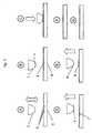
- a high-viscosity printing paste 2is removed from the printing plate 3 by means of a rubber stamp 1 .
- said rubber stamp 1consists of a material resistant to the reactive printing paste 2 .
- siliconeis most suitable due to its resistance to swelling and acid.
- Said printing plate 3contains said printing paste as a negative printing plate of the strip conductors or electrodes to be produced.
- said printing paste 2is applied by means of said rubber stamp 1 , to a substrate 5 , which is coated with a conductive layer 4 .
- Said printing paste 2adheres to said rubber stamp 1 in the shape of discrete structures, enabling said conductive layer 4 to be treated for structuring.
- said conductive layer 4is comprised of a conductive metallic layer between 1 and 100 nm, such as, for example, gold, aluminum, copper or ITO, which had been vacuum-deposited.
- Said printing paste 2comprises corrosive characteristics, exhibiting a content of ferric chloride in the case of the application with copper, a content of iodine/potassium iodide in the case of the application with gold, a content of haloid acid in the case of the application with ITO, and a content of hydrochloric acid or sodium hydroxide in the case of the application with aluminum.
- the substratecan be chosen freely and may therefore be a silicon carrier or a thin layer of glass.
- the substratecan be chosen freely and may therefore be a silicon carrier or a thin layer of glass.
- very thin flexible plastic filmsmade of, for example,
- polyethylene, polyethylene terephthalate or polyimidewill be used.
- Said conductive layer 4does also not have to be deposited directly on said carrier substrate 5 .
- the layer beneathcan also be a partially finished, optoelectronic component, which already displays structured functional layers.
- step Dsaid printing paste is characterized in that a conductive inorganic layer 6 , according to the printing structure, adheres to the adhesive print medium and can therefore be directly removed from the substrate.
- This processcan be repeated several times, if need be, provided that said removed conductive layer 6 dissolves in said print medium, in each case.
- Conductive structure 7remains, which can be processed, for example, to build up an OFET or another optoelectronic component.
- said rubber stamp 1also called tampon, must be cleaned afterwards in order to repeat said process step.
- Said processcan be performed by means of an intermediate step, which will not be detailed here, in which said rubber stamp 1 is immersed into a suitable solvent.
- said printing paste 3is directly transferred to said conductive layer 4 (Step E).
- a structured printing paste 9 and said conductive layer 4react with one another and said conductive layer 4 is detached from said stamp 1 in the areas containing the prints (Step F).
- Remaining residue 8 at said stamp 1must be removed.
- the processmust be stopped through neutralization in a base, without said base reacting with said conductive layer.
- Step Gdemonstrates how the structure, after neutralization and removal
- [0027]is formed in said conductive layer.
- additional processing stepsas described hereinabove, may follow.
Landscapes
- Engineering & Computer Science (AREA)
- Manufacturing & Machinery (AREA)
- Microelectronics & Electronic Packaging (AREA)
- Physics & Mathematics (AREA)
- Optics & Photonics (AREA)
- Electroluminescent Light Sources (AREA)
- Manufacturing Of Printed Wiring (AREA)
Abstract
Description
- A method for producing conductive structures by means of a printing technique as well as active components produced thereof for integrated circuits.[0001]
- The invention relates to a method for producing conductive structures as well as active components produced thereof, in particular, organic field-effect transistors (OFETs), organic light-emitting diodes (OLEDs) or integrated circuits comprised thereof.[0002]
- Conductive and finely structured electrodes or strip conductors, which can be produced from conductive materials such as metals, organically conductive polymers or polymers filled with particles, are required to realize organic or inorganic optoelectronic components. Hereby, organic layers can be structured photochemically (see C. J. Drury et al., Applied Physics Letter 73 (1) (1998) 108 and G. H. Gelink et al., Applied Physics Letter 77 (10) 2000, 1,487), or by means of lithography (synthetic method 101 (1999) 705). Similar methods are also possible to structure inorganic conductive layers).[0003]
- Said methods for structuring conductive layers or generating strip conductors or electrodes are very complex in terms of working techniques and thus very time-consuming and costly. Therefore, these processes are too extensive, in particular, for producing high-resolution conductive structures in optoelectronic components, such as OFETs, OLEDs and the like.[0004]
- The applicant's [patent] DE 10047171.4, which has not yet been published, describes a method for producing an electrode and/or a strip conductor comprised of organic material through contact with a chemical compound. Organic[0005]
- materials have a disadvantage in that they are not as stable as corresponding inorganic materials.[0006]
- It is therefore the purpose of the present invention to specify a method enabling the production of high-resolution conductive structures comprised of inorganic material, if possible, in a simple and cost-effective process and with as few procedures as possible.[0007]
- Therefore, the object of the present invention is a method for producing conductive layers characterized in that strip conductors or electrodes are produced in a conductive layer by means of a printing technique.[0008]
- The method is rendered substantially simpler, cheaper and quicker due to printable structuring. In addition, all procedures, which are required, for example, for lithography, such as the application of photosensitive resist, light exposure, development and subsequent cleaning, if applicable, can be omitted.[0009]
- In principal, all printing methods, such as gravure, letterpress, planographic and through printing (screen printing) are suitable. However, a particularly preferred embodiment according to the present invention is the production of strip conductors or electrodes by means of the so-called offset gravure printing method. This is called tampon printing. The advantage of this printing method is characterized in that the structure to be generated can be connected positively or negatively in the shape of a printing plate that contains the printing paste.[0010]
- It is the advantage of the method according to the present invention that it is suitable for producing organic as well as inorganic conductive structures or strip conductors or electrodes.[0011]
- A preferred conductive organic layer, for example, is doped polyaniline, in which a non-conducting matrix is produced through printing with an alkaline print medium using deprotonation.[0012]
- A conductive structure in a non-conducting matrix can also be produced by printing non-doped polyaniline with an acidic print medium by means of protonation. Said matrix can then be removed and, if appropriate, filled in with a semiconducting layer. For reasons of stability of the optoelectronic component, which contains a conductive, structured layer produced in accordance with the present invention, it is advantageous to choose said layer from inorganic conductive material, preferably gold, aluminum, copper or indium tin oxide (ITO). At first, a metallic conductive layer, which, for example, can be between 1 and 100 nm thick, is applied by vacuum deposition, for example, on a substrate or a lower layer. Then, a suitable, negative resist paste is printed on the strip conductor or electrode to be produced by means of the offset gravure printing method, whereby the conductive layer in the printed areas is etched away by forming strip conductors or electrodes. Also, a resist paste, which is removed after the etching process, can be printed inversely positive.[0013]
- Said paste may have alkaline or acidic characteristics, depending on the conductive layer to be produced.[0014]
- It is advantageous that the method according to the invention is developed in a continuous fashion, which guarantees mass production.[0015]
- The invention also concerns an organic field-effect transistor, whereby source, drain and/or gate electrodes are produced according to the method of the present invention.[0016]
- The invention also concerns organic light-emitting diodes, whereby conductive structures are formed in accordance with the method of the present invention.[0017]
- The invention also concerns organic diodes, in particular, rectifier diodes.[0018]
- The invention also concerns integrated circuits comprising at least one OFET or another active component, said component being produced in accordance with the method of the present invention.[0019]
- Below, the invention is described in detail using an embodiment example and the enclosed FIG. 1.[0020]
- During step A, a high-[0021]
viscosity printing paste 2 is removed from theprinting plate 3 by means of a rubber stamp1. Preferably, said rubber stamp1 consists of a material resistant to thereactive printing paste 2. In order to form inorganic strip conductors or electrodes, silicone is most suitable due to its resistance to swelling and acid. Saidprinting plate 3 contains said printing paste as a negative printing plate of the strip conductors or electrodes to be produced. During steps B and C, saidprinting paste 2 is applied by means of said rubber stamp1, to asubstrate 5, which is coated with a conductive layer4. Said printing paste2 adheres to said rubber stamp1 in the shape of discrete structures, enabling said conductive layer4 to be treated for structuring. In the specified embodiment, said conductive layer4 is comprised of a conductive metallic layer between 1 and 100 nm, such as, for example, gold, aluminum, copper or ITO, which had been vacuum-deposited. Saidprinting paste 2 comprises corrosive characteristics, exhibiting a content of ferric chloride in the case of the application with copper, a content of iodine/potassium iodide in the case of the application with gold, a content of haloid acid in the case of the application with ITO, and a content of hydrochloric acid or sodium hydroxide in the case of the application with aluminum. - In principal, the substrate can be chosen freely and may therefore be a silicon carrier or a thin layer of glass. Preferably, however, very thin flexible plastic films made of, for example,[0022]
- polyethylene, polyethylene terephthalate or polyimide will be used. Said conductive layer[0023]4 does also not have to be deposited directly on said
carrier substrate 5. The layer beneath can also be a partially finished, optoelectronic component, which already displays structured functional layers. - In principal, there are two different processing steps depending on the characteristics of the used printing paste, which will be explained below:[0024]
- According to step D, said printing paste is characterized in that a conductive[0025]
inorganic layer 6, according to the printing structure, adheres to the adhesive print medium and can therefore be directly removed from the substrate. This process can be repeated several times, if need be, provided that said removedconductive layer 6 dissolves in said print medium, in each case. Conductive structure7 remains, which can be processed, for example, to build up an OFET or another optoelectronic component. Using this method, said rubber stamp1, also called tampon, must be cleaned afterwards in order to repeat said process step. Said process can be performed by means of an intermediate step, which will not be detailed here, in which said rubber stamp1 is immersed into a suitable solvent. - According to another embodiment or by means of a different print medium, said[0026]
printing paste 3 is directly transferred to said conductive layer4 (Step E). Astructured printing paste 9 and said conductive layer4 react with one another and said conductive layer4 is detached from said stamp1 in the areas containing the prints (Step F). Remainingresidue 8 at said stamp1 must be removed. In order to avoid high lateral corrosion, the process must be stopped through neutralization in a base, without said base reacting with said conductive layer. Step G demonstrates how the structure, after neutralization and removal, - is formed in said conductive layer. Here, too, additional processing steps, as described hereinabove, may follow.[0027]
Claims (12)
1. A method for producing conductive structures, characterized in that strip conductors and/or electrodes can be directly or indirectly produced inside said conductive layer (4) by means of a printing technique.
2. A method in accordance withclaim 1 , characterized in that strip conductors and/or electrodes can be produced using the offset gravure printing method by applying said reactive printing paste (3).
3. A method in accordance withclaim 1 or2, characterized in that an organic conductive layer is produced and structured by means of the offset gravure printing method.
4. A method in accordance withclaim 4 , characterized in that the conductive organic layer is doped polyaniline, in which a non-conducting matrix is produced through printing with an alkaline medium using deprotonation.
5. A method in accordance withclaim 4 , characterized in that the conductive organic layer is non-doped polyaniline, in which a non-conducting matrix is produced through printing with an acid medium using deprotonation.
6. A method in accordance withclaim 1 or2, characterized in that said inorganic conductive layer is produced.
7. A method in accordance withclaim 6 , characterized in that said conductive inorganic layer from [missing text]
8. A method in accordance with claims1 through7, characterized in that said printing process is performed continuously.
9. An organic field-effect transistor, whereby source, drain and/or gate electrodes are formed using a method in accordance with claims1 through8.
10. A light-emitting electrode, whereby conductive structures are formed using a method in accordance with claims1 through8.
11. An organic (rectifier) diode, whereby conductive structures are formed using a method in accordance with claims1 through8.
12. Integrated circuits comprising at least one active component in accordance with one of claims9 through11.
Applications Claiming Priority (3)
| Application Number | Priority Date | Filing Date | Title |
|---|---|---|---|
| DE10126859.9 | 2001-06-01 | ||
| DE10126859ADE10126859A1 (en) | 2001-06-01 | 2001-06-01 | Production of conducting structures used in organic FETs, illuminated diodes, organic diodes and integrated circuits comprises directly or indirectly forming conducting pathways |
| PCT/DE2002/001717WO2002099908A1 (en) | 2001-06-01 | 2002-05-13 | Method for producing conductive structures by means of a printing technique, and active components produced therefrom for integrated circuits |
Publications (1)
| Publication Number | Publication Date |
|---|---|
| US20040209191A1true US20040209191A1 (en) | 2004-10-21 |
Family
ID=7686980
Family Applications (1)
| Application Number | Title | Priority Date | Filing Date |
|---|---|---|---|
| US10/479,238AbandonedUS20040209191A1 (en) | 2001-06-01 | 2002-05-13 | Method for producing conductive structures by means of printing technique, and active components produced therefrom for integrated circuits |
Country Status (4)
| Country | Link |
|---|---|
| US (1) | US20040209191A1 (en) |
| EP (1) | EP1393388A1 (en) |
| DE (1) | DE10126859A1 (en) |
| WO (1) | WO2002099908A1 (en) |
Cited By (5)
| Publication number | Priority date | Publication date | Assignee | Title |
|---|---|---|---|---|
| US20030183817A1 (en)* | 2000-09-01 | 2003-10-02 | Adolf Bernds | Organic field effect transistor, method for structuring an ofet and integrated circuit |
| US20050163932A1 (en)* | 2002-08-30 | 2005-07-28 | Ute Zschieschang | Fabrication of organic electronic circuits by contact printing techniques |
| US20060273305A1 (en)* | 2005-06-07 | 2006-12-07 | Yaron Grinwald | Printing conductive patterns using LEP |
| US20100033213A1 (en)* | 2006-10-06 | 2010-02-11 | Andreas Ullmann | Field effect transistor and electric circuit |
| US8315061B2 (en)* | 2005-09-16 | 2012-11-20 | Polyic Gmbh & Co. Kg | Electronic circuit with elongated strip layer and method for the manufacture of the same |
Families Citing this family (21)
| Publication number | Priority date | Publication date | Assignee | Title |
|---|---|---|---|---|
| DE10061299A1 (en) | 2000-12-08 | 2002-06-27 | Siemens Ag | Device for determining and / or forwarding at least one environmental influence, production method and use thereof |
| DE10061297C2 (en) | 2000-12-08 | 2003-05-28 | Siemens Ag | Procedure for structuring an OFET |
| DE10105914C1 (en) | 2001-02-09 | 2002-10-10 | Siemens Ag | Organic field effect transistor with photo-structured gate dielectric and a method for its production |
| DE10151036A1 (en) | 2001-10-16 | 2003-05-08 | Siemens Ag | Isolator for an organic electronic component |
| DE10151440C1 (en) | 2001-10-18 | 2003-02-06 | Siemens Ag | Organic electronic component for implementing an encapsulated partially organic electronic component has components like a flexible foil as an antenna, a diode or capacitor and an organic transistor. |
| DE10160732A1 (en) | 2001-12-11 | 2003-06-26 | Siemens Ag | OFET used e.g. in RFID tag, comprises an intermediate layer on an active semiconductor layer |
| DE10212640B4 (en) | 2002-03-21 | 2004-02-05 | Siemens Ag | Logical components made of organic field effect transistors |
| US6773614B2 (en)* | 2002-04-16 | 2004-08-10 | Hewlett-Packard Development Company, L.P. | Method of patterning conductive films |
| DE10253154A1 (en) | 2002-11-14 | 2004-05-27 | Siemens Ag | Biosensor, used to identify analyte in liquid sample, has test field with detector, where detector registers field changes as electrical signals for evaluation |
| EP1563553B1 (en) | 2002-11-19 | 2007-02-14 | PolyIC GmbH & Co. KG | Organic electronic circuitcomprising a structured, semi-conductive functional layer and a method for producing said component |
| DE10302149A1 (en) | 2003-01-21 | 2005-08-25 | Siemens Ag | Use of conductive carbon black / graphite blends for the production of low-cost electronics |
| US20060160266A1 (en)* | 2003-01-21 | 2006-07-20 | Adolf Bernds | Organic electronic component and method for producing organic electronic devices |
| DE10330062A1 (en)* | 2003-07-03 | 2005-01-27 | Siemens Ag | Method and device for structuring organic layers |
| DE10339036A1 (en) | 2003-08-25 | 2005-03-31 | Siemens Ag | Organic electronic component with high-resolution structuring and manufacturing method |
| DE10340644B4 (en) | 2003-09-03 | 2010-10-07 | Polyic Gmbh & Co. Kg | Mechanical controls for organic polymer electronics |
| DE102004031719A1 (en)* | 2004-06-30 | 2006-01-19 | Infineon Technologies Ag | Production process for an electrically functional layer structure for semiconductor technology forms and applies mask by gravure process and structures a material layer |
| DE102005009820A1 (en) | 2005-03-01 | 2006-09-07 | Polyic Gmbh & Co. Kg | Electronic assembly with organic logic switching elements |
| DE102005017655B4 (en) | 2005-04-15 | 2008-12-11 | Polyic Gmbh & Co. Kg | Multilayer composite body with electronic function |
| DE102005031448A1 (en) | 2005-07-04 | 2007-01-11 | Polyic Gmbh & Co. Kg | Activatable optical layer |
| DE102005035589A1 (en) | 2005-07-29 | 2007-02-01 | Polyic Gmbh & Co. Kg | Manufacturing electronic component on surface of substrate where component has two overlapping function layers |
| DE102007062944B4 (en) | 2007-12-21 | 2016-03-17 | Leonhard Kurz Stiftung & Co. Kg | Electronic switch |
Citations (54)
| Publication number | Priority date | Publication date | Assignee | Title |
|---|---|---|---|---|
| US3512052A (en)* | 1968-01-11 | 1970-05-12 | Gen Motors Corp | Metal-insulator-semiconductor voltage variable capacitor with controlled resistivity dielectric |
| US3955098A (en)* | 1973-10-12 | 1976-05-04 | Hitachi, Ltd. | Switching circuit having floating gate mis load transistors |
| US4302648A (en)* | 1978-01-26 | 1981-11-24 | Shin-Etsu Polymer Co., Ltd. | Key-board switch unit |
| US4442019A (en)* | 1978-05-26 | 1984-04-10 | Marks Alvin M | Electroordered dipole suspension |
| US4865197A (en)* | 1988-03-04 | 1989-09-12 | Unisys Corporation | Electronic component transportation container |
| US4926052A (en)* | 1986-03-03 | 1990-05-15 | Kabushiki Kaisha Toshiba | Radiation detecting device |
| US5173835A (en)* | 1991-10-15 | 1992-12-22 | Motorola, Inc. | Voltage variable capacitor |
| US5259926A (en)* | 1991-09-24 | 1993-11-09 | Hitachi, Ltd. | Method of manufacturing a thin-film pattern on a substrate |
| US5321240A (en)* | 1992-01-30 | 1994-06-14 | Mitsubishi Denki Kabushiki Kaisha | Non-contact IC card |
| US5480839A (en)* | 1993-01-15 | 1996-01-02 | Kabushiki Kaisha Toshiba | Semiconductor device manufacturing method |
| US5546889A (en)* | 1993-10-06 | 1996-08-20 | Matsushita Electric Industrial Co., Ltd. | Method of manufacturing organic oriented film and method of manufacturing electronic device |
| US5569879A (en)* | 1991-02-19 | 1996-10-29 | Gemplus Card International | Integrated circuit micromodule obtained by the continuous assembly of patterned strips |
| US5578513A (en)* | 1993-09-17 | 1996-11-26 | Mitsubishi Denki Kabushiki Kaisha | Method of making a semiconductor device having a gate all around type of thin film transistor |
| US5652645A (en)* | 1995-07-24 | 1997-07-29 | Anvik Corporation | High-throughput, high-resolution, projection patterning system for large, flexible, roll-fed, electronic-module substrates |
| US5729428A (en)* | 1995-04-25 | 1998-03-17 | Nec Corporation | Solid electrolytic capacitor with conductive polymer as solid electrolyte and method for fabricating the same |
| US5869972A (en)* | 1996-02-26 | 1999-02-09 | Birch; Brian Jeffrey | Testing device using a thermochromic display and method of using same |
| US5892244A (en)* | 1989-01-10 | 1999-04-06 | Mitsubishi Denki Kabushiki Kaisha | Field effect transistor including πconjugate polymer and liquid crystal display including the field effect transistor |
| US5925259A (en)* | 1995-08-04 | 1999-07-20 | International Business Machines Corporation | Lithographic surface or thin layer modification |
| US5967048A (en)* | 1998-06-12 | 1999-10-19 | Howard A. Fromson | Method and apparatus for the multiple imaging of a continuous web |
| US5994773A (en)* | 1996-03-06 | 1999-11-30 | Hirakawa; Tadashi | Ball grid array semiconductor package |
| US6027595A (en)* | 1998-07-02 | 2000-02-22 | Samsung Electronics Co., Ltd. | Method of making optical replicas by stamping in photoresist and replicas formed thereby |
| US6045977A (en)* | 1998-02-19 | 2000-04-04 | Lucent Technologies Inc. | Process for patterning conductive polyaniline films |
| US6083104A (en)* | 1998-01-16 | 2000-07-04 | Silverlit Toys (U.S.A.), Inc. | Programmable toy with an independent game cartridge |
| US6143412A (en)* | 1997-02-10 | 2000-11-07 | President And Fellows Of Harvard College | Fabrication of carbon microstructures |
| US6197663B1 (en)* | 1999-12-07 | 2001-03-06 | Lucent Technologies Inc. | Process for fabricating integrated circuit devices having thin film transistors |
| US6215130B1 (en)* | 1998-08-20 | 2001-04-10 | Lucent Technologies Inc. | Thin film transistors |
| US6251513B1 (en)* | 1997-11-08 | 2001-06-26 | Littlefuse, Inc. | Polymer composites for overvoltage protection |
| US6284562B1 (en)* | 1999-11-17 | 2001-09-04 | Agere Systems Guardian Corp. | Thin film transistors |
| US6321571B1 (en)* | 1998-12-21 | 2001-11-27 | Corning Incorporated | Method of making glass structures for flat panel displays |
| US6322736B1 (en)* | 1998-03-27 | 2001-11-27 | Agere Systems Inc. | Method for fabricating molded microstructures on substrates |
| US6329226B1 (en)* | 2000-06-01 | 2001-12-11 | Agere Systems Guardian Corp. | Method for fabricating a thin-film transistor |
| US6335539B1 (en)* | 1999-11-05 | 2002-01-01 | International Business Machines Corporation | Method for improving performance of organic semiconductors in bottom electrode structure |
| US6340822B1 (en)* | 1999-10-05 | 2002-01-22 | Agere Systems Guardian Corp. | Article comprising vertically nano-interconnected circuit devices and method for making the same |
| US6344662B1 (en)* | 1997-03-25 | 2002-02-05 | International Business Machines Corporation | Thin-film field-effect transistor with organic-inorganic hybrid semiconductor requiring low operating voltages |
| US20020018911A1 (en)* | 1999-05-11 | 2002-02-14 | Mark T. Bernius | Electroluminescent or photocell device having protective packaging |
| US20020022284A1 (en)* | 1991-02-27 | 2002-02-21 | Alan J. Heeger | Visible light emitting diodes fabricated from soluble semiconducting polymers |
| US20020025391A1 (en)* | 1989-05-26 | 2002-02-28 | Marie Angelopoulos | Patterns of electrically conducting polymers and their application as electrodes or electrical contacts |
| US20020053320A1 (en)* | 1998-12-15 | 2002-05-09 | Gregg M. Duthaler | Method for printing of transistor arrays on plastic substrates |
| US20020056839A1 (en)* | 2000-11-11 | 2002-05-16 | Pt Plus Co. Ltd. | Method of crystallizing a silicon thin film and semiconductor device fabricated thereby |
| US20020068392A1 (en)* | 2000-12-01 | 2002-06-06 | Pt Plus Co. Ltd. | Method for fabricating thin film transistor including crystalline silicon active layer |
| US6468819B1 (en)* | 1999-11-23 | 2002-10-22 | The Trustees Of Princeton University | Method for patterning organic thin film devices using a die |
| US20020170897A1 (en)* | 2001-05-21 | 2002-11-21 | Hall Frank L. | Methods for preparing ball grid array substrates via use of a laser |
| US20020179898A1 (en)* | 1996-06-25 | 2002-12-05 | Tobin J. Marks | Organic light-emitting diodes and methods for assembly and emission control |
| US6498114B1 (en)* | 1999-04-09 | 2002-12-24 | E Ink Corporation | Method for forming a patterned semiconductor film |
| US20020195644A1 (en)* | 2001-06-08 | 2002-12-26 | Ananth Dodabalapur | Organic polarizable gate transistor apparatus and method |
| US6517995B1 (en)* | 1999-09-14 | 2003-02-11 | Massachusetts Institute Of Technology | Fabrication of finely featured devices by liquid embossing |
| US6541539B1 (en)* | 1998-11-04 | 2003-04-01 | President And Fellows Of Harvard College | Hierarchically ordered porous oxides |
| US20030112576A1 (en)* | 2001-09-28 | 2003-06-19 | Brewer Peter D. | Process for producing high performance interconnects |
| US6586791B1 (en)* | 2000-07-19 | 2003-07-01 | 3M Innovative Properties Company | Transistor insulator layer incorporating superfine ceramic particles |
| US20030175427A1 (en)* | 2002-03-15 | 2003-09-18 | Yeuh-Lin Loo | Forming nanoscale patterned thin film metal layers |
| US20040002176A1 (en)* | 2002-06-28 | 2004-01-01 | Xerox Corporation | Organic ferroelectric memory cells |
| US20040026689A1 (en)* | 2000-08-18 | 2004-02-12 | Adolf Bernds | Encapsulated organic-electronic component, method for producing the same and use thereof |
| US20040211329A1 (en)* | 2001-09-18 | 2004-10-28 | Katsuyuki Funahata | Pattern forming method and pattern forming device |
| US6852583B2 (en)* | 2000-07-07 | 2005-02-08 | Siemens Aktiengesellschaft | Method for the production and configuration of organic field-effect transistors (OFET) |
Family Cites Families (2)
| Publication number | Priority date | Publication date | Assignee | Title |
|---|---|---|---|---|
| TW556357B (en)* | 1999-06-28 | 2003-10-01 | Semiconductor Energy Lab | Method of manufacturing an electro-optical device |
| WO2001017041A1 (en)* | 1999-08-31 | 2001-03-08 | E Ink Corporation | Method for forming a patterned semiconductor film |
- 2001
- 2001-06-01DEDE10126859Apatent/DE10126859A1/ennot_activeCeased
- 2002
- 2002-05-13WOPCT/DE2002/001717patent/WO2002099908A1/ennot_activeApplication Discontinuation
- 2002-05-13EPEP02726090Apatent/EP1393388A1/ennot_activeWithdrawn
- 2002-05-13USUS10/479,238patent/US20040209191A1/ennot_activeAbandoned
Patent Citations (55)
| Publication number | Priority date | Publication date | Assignee | Title |
|---|---|---|---|---|
| US3512052A (en)* | 1968-01-11 | 1970-05-12 | Gen Motors Corp | Metal-insulator-semiconductor voltage variable capacitor with controlled resistivity dielectric |
| US3955098A (en)* | 1973-10-12 | 1976-05-04 | Hitachi, Ltd. | Switching circuit having floating gate mis load transistors |
| US4302648A (en)* | 1978-01-26 | 1981-11-24 | Shin-Etsu Polymer Co., Ltd. | Key-board switch unit |
| US4442019A (en)* | 1978-05-26 | 1984-04-10 | Marks Alvin M | Electroordered dipole suspension |
| US4926052A (en)* | 1986-03-03 | 1990-05-15 | Kabushiki Kaisha Toshiba | Radiation detecting device |
| US4865197A (en)* | 1988-03-04 | 1989-09-12 | Unisys Corporation | Electronic component transportation container |
| US5892244A (en)* | 1989-01-10 | 1999-04-06 | Mitsubishi Denki Kabushiki Kaisha | Field effect transistor including πconjugate polymer and liquid crystal display including the field effect transistor |
| US20020025391A1 (en)* | 1989-05-26 | 2002-02-28 | Marie Angelopoulos | Patterns of electrically conducting polymers and their application as electrodes or electrical contacts |
| US5569879A (en)* | 1991-02-19 | 1996-10-29 | Gemplus Card International | Integrated circuit micromodule obtained by the continuous assembly of patterned strips |
| US20020022284A1 (en)* | 1991-02-27 | 2002-02-21 | Alan J. Heeger | Visible light emitting diodes fabricated from soluble semiconducting polymers |
| US5259926A (en)* | 1991-09-24 | 1993-11-09 | Hitachi, Ltd. | Method of manufacturing a thin-film pattern on a substrate |
| US5173835A (en)* | 1991-10-15 | 1992-12-22 | Motorola, Inc. | Voltage variable capacitor |
| US5321240A (en)* | 1992-01-30 | 1994-06-14 | Mitsubishi Denki Kabushiki Kaisha | Non-contact IC card |
| US5480839A (en)* | 1993-01-15 | 1996-01-02 | Kabushiki Kaisha Toshiba | Semiconductor device manufacturing method |
| US5578513A (en)* | 1993-09-17 | 1996-11-26 | Mitsubishi Denki Kabushiki Kaisha | Method of making a semiconductor device having a gate all around type of thin film transistor |
| US5546889A (en)* | 1993-10-06 | 1996-08-20 | Matsushita Electric Industrial Co., Ltd. | Method of manufacturing organic oriented film and method of manufacturing electronic device |
| US5729428A (en)* | 1995-04-25 | 1998-03-17 | Nec Corporation | Solid electrolytic capacitor with conductive polymer as solid electrolyte and method for fabricating the same |
| US5652645A (en)* | 1995-07-24 | 1997-07-29 | Anvik Corporation | High-throughput, high-resolution, projection patterning system for large, flexible, roll-fed, electronic-module substrates |
| US5925259A (en)* | 1995-08-04 | 1999-07-20 | International Business Machines Corporation | Lithographic surface or thin layer modification |
| US5869972A (en)* | 1996-02-26 | 1999-02-09 | Birch; Brian Jeffrey | Testing device using a thermochromic display and method of using same |
| US5994773A (en)* | 1996-03-06 | 1999-11-30 | Hirakawa; Tadashi | Ball grid array semiconductor package |
| US20020179898A1 (en)* | 1996-06-25 | 2002-12-05 | Tobin J. Marks | Organic light-emitting diodes and methods for assembly and emission control |
| US6143412A (en)* | 1997-02-10 | 2000-11-07 | President And Fellows Of Harvard College | Fabrication of carbon microstructures |
| US6344662B1 (en)* | 1997-03-25 | 2002-02-05 | International Business Machines Corporation | Thin-film field-effect transistor with organic-inorganic hybrid semiconductor requiring low operating voltages |
| US6251513B1 (en)* | 1997-11-08 | 2001-06-26 | Littlefuse, Inc. | Polymer composites for overvoltage protection |
| US6083104A (en)* | 1998-01-16 | 2000-07-04 | Silverlit Toys (U.S.A.), Inc. | Programmable toy with an independent game cartridge |
| US6045977A (en)* | 1998-02-19 | 2000-04-04 | Lucent Technologies Inc. | Process for patterning conductive polyaniline films |
| US6322736B1 (en)* | 1998-03-27 | 2001-11-27 | Agere Systems Inc. | Method for fabricating molded microstructures on substrates |
| US5967048A (en)* | 1998-06-12 | 1999-10-19 | Howard A. Fromson | Method and apparatus for the multiple imaging of a continuous web |
| US6027595A (en)* | 1998-07-02 | 2000-02-22 | Samsung Electronics Co., Ltd. | Method of making optical replicas by stamping in photoresist and replicas formed thereby |
| US6215130B1 (en)* | 1998-08-20 | 2001-04-10 | Lucent Technologies Inc. | Thin film transistors |
| US6541539B1 (en)* | 1998-11-04 | 2003-04-01 | President And Fellows Of Harvard College | Hierarchically ordered porous oxides |
| US20020053320A1 (en)* | 1998-12-15 | 2002-05-09 | Gregg M. Duthaler | Method for printing of transistor arrays on plastic substrates |
| US6321571B1 (en)* | 1998-12-21 | 2001-11-27 | Corning Incorporated | Method of making glass structures for flat panel displays |
| US6498114B1 (en)* | 1999-04-09 | 2002-12-24 | E Ink Corporation | Method for forming a patterned semiconductor film |
| US20020018911A1 (en)* | 1999-05-11 | 2002-02-14 | Mark T. Bernius | Electroluminescent or photocell device having protective packaging |
| US20040013982A1 (en)* | 1999-09-14 | 2004-01-22 | Massachusetts Institute Of Technology | Fabrication of finely featured devices by liquid embossing |
| US6517995B1 (en)* | 1999-09-14 | 2003-02-11 | Massachusetts Institute Of Technology | Fabrication of finely featured devices by liquid embossing |
| US6340822B1 (en)* | 1999-10-05 | 2002-01-22 | Agere Systems Guardian Corp. | Article comprising vertically nano-interconnected circuit devices and method for making the same |
| US6335539B1 (en)* | 1999-11-05 | 2002-01-01 | International Business Machines Corporation | Method for improving performance of organic semiconductors in bottom electrode structure |
| US6284562B1 (en)* | 1999-11-17 | 2001-09-04 | Agere Systems Guardian Corp. | Thin film transistors |
| US6468819B1 (en)* | 1999-11-23 | 2002-10-22 | The Trustees Of Princeton University | Method for patterning organic thin film devices using a die |
| US6197663B1 (en)* | 1999-12-07 | 2001-03-06 | Lucent Technologies Inc. | Process for fabricating integrated circuit devices having thin film transistors |
| US6329226B1 (en)* | 2000-06-01 | 2001-12-11 | Agere Systems Guardian Corp. | Method for fabricating a thin-film transistor |
| US6852583B2 (en)* | 2000-07-07 | 2005-02-08 | Siemens Aktiengesellschaft | Method for the production and configuration of organic field-effect transistors (OFET) |
| US6586791B1 (en)* | 2000-07-19 | 2003-07-01 | 3M Innovative Properties Company | Transistor insulator layer incorporating superfine ceramic particles |
| US20040026689A1 (en)* | 2000-08-18 | 2004-02-12 | Adolf Bernds | Encapsulated organic-electronic component, method for producing the same and use thereof |
| US20020056839A1 (en)* | 2000-11-11 | 2002-05-16 | Pt Plus Co. Ltd. | Method of crystallizing a silicon thin film and semiconductor device fabricated thereby |
| US20020068392A1 (en)* | 2000-12-01 | 2002-06-06 | Pt Plus Co. Ltd. | Method for fabricating thin film transistor including crystalline silicon active layer |
| US20020170897A1 (en)* | 2001-05-21 | 2002-11-21 | Hall Frank L. | Methods for preparing ball grid array substrates via use of a laser |
| US20020195644A1 (en)* | 2001-06-08 | 2002-12-26 | Ananth Dodabalapur | Organic polarizable gate transistor apparatus and method |
| US20040211329A1 (en)* | 2001-09-18 | 2004-10-28 | Katsuyuki Funahata | Pattern forming method and pattern forming device |
| US20030112576A1 (en)* | 2001-09-28 | 2003-06-19 | Brewer Peter D. | Process for producing high performance interconnects |
| US20030175427A1 (en)* | 2002-03-15 | 2003-09-18 | Yeuh-Lin Loo | Forming nanoscale patterned thin film metal layers |
| US20040002176A1 (en)* | 2002-06-28 | 2004-01-01 | Xerox Corporation | Organic ferroelectric memory cells |
Cited By (9)
| Publication number | Priority date | Publication date | Assignee | Title |
|---|---|---|---|---|
| US20030183817A1 (en)* | 2000-09-01 | 2003-10-02 | Adolf Bernds | Organic field effect transistor, method for structuring an ofet and integrated circuit |
| US20050163932A1 (en)* | 2002-08-30 | 2005-07-28 | Ute Zschieschang | Fabrication of organic electronic circuits by contact printing techniques |
| US7396566B2 (en) | 2002-08-30 | 2008-07-08 | Infineon Technologies, Ag | Fabrication of organic electronic circuits by contact printing techniques |
| US20060273305A1 (en)* | 2005-06-07 | 2006-12-07 | Yaron Grinwald | Printing conductive patterns using LEP |
| US7476603B2 (en) | 2005-06-07 | 2009-01-13 | Hewlett-Packard Development Company, L.P. | Printing conductive patterns using LEP |
| US20090085462A1 (en)* | 2005-06-07 | 2009-04-02 | Yaron Grinwald | Printing Conductive Patterns Using LEP |
| US8315061B2 (en)* | 2005-09-16 | 2012-11-20 | Polyic Gmbh & Co. Kg | Electronic circuit with elongated strip layer and method for the manufacture of the same |
| US20100033213A1 (en)* | 2006-10-06 | 2010-02-11 | Andreas Ullmann | Field effect transistor and electric circuit |
| US8217432B2 (en) | 2006-10-06 | 2012-07-10 | Polyic Gmbh & Co. Kg | Field effect transistor and electric circuit |
Also Published As
| Publication number | Publication date |
|---|---|
| WO2002099908A1 (en) | 2002-12-12 |
| EP1393388A1 (en) | 2004-03-03 |
| DE10126859A1 (en) | 2002-12-12 |
Similar Documents
| Publication | Publication Date | Title |
|---|---|---|
| US20040209191A1 (en) | Method for producing conductive structures by means of printing technique, and active components produced therefrom for integrated circuits | |
| AU2004283127B2 (en) | Method for production of a film | |
| US9159925B2 (en) | Process for imprint patterning materials in thin-film devices | |
| CN1967384B (en) | Stamp and fabricating method thereof, thin film transistor using the stamp, and liquid crystal display device having the thin film transistor | |
| US20080012151A1 (en) | Method and an Apparatus for Manufacturing an Electronic Thin-Film Component and an Electronic Thin-Film Component | |
| EP1596446A2 (en) | Apparatus and method for producing an electronic component comprising at least one active organic layer | |
| JP4439394B2 (en) | Pattern formation method | |
| JP2004503116A (en) | Method of manufacturing and structuring an organic field effect transistor (OFET) | |
| CN101034667A (en) | Device fabrication by ink-jet printing materials into bank structures, and embossing tool | |
| CN106575607A (en) | Orthogonal patterning method | |
| JP2007268715A (en) | Printing method, electrode pattern forming method, and thin film transistor forming method | |
| CN108493229A (en) | Display base plate and preparation method thereof, display device | |
| US20040026121A1 (en) | Electrode and/or conductor track for organic components and production method thereof | |
| EP1974400B1 (en) | Method of fabricating a semiconductor device | |
| JP5729540B2 (en) | Field effect transistor and manufacturing method thereof | |
| JP5481893B2 (en) | Organic transistor active substrate, organic transistor active substrate manufacturing method, and electrophoretic display using organic transistor active substrate | |
| RU2515340C2 (en) | Method of electronic device fabrication | |
| JP2006073794A (en) | Field effect transistor and manufacturing method thereof | |
| US8202771B2 (en) | Manufacturing method of organic semiconductor device | |
| KR20080026990A (en) | Thin film transistor, display device having same and manufacturing method thereof | |
| CN101536204A (en) | Conductive polymer electrode | |
| JP2009056685A (en) | Plate and plate forming method used for reverse offset printing, relief printing and intaglio printing, and printed matter forming method | |
| Kahn | Organic Electronics Technology | |
| JP2004281623A (en) | Thin film transistor element sheet and method of manufacturing thin film transistor element sheet | |
| JP2006237197A (en) | Thin film transistor manufacturing method |
Legal Events
| Date | Code | Title | Description |
|---|---|---|---|
| AS | Assignment | Owner name:SIEMENS AKTIENGESELLSCHAFT, GERMANY Free format text:ASSIGNMENT OF ASSIGNORS INTEREST;ASSIGNORS:BERNDS, ADOLF;CLEMENS, WOLFGANG;FIX, WALTER;AND OTHERS;REEL/FRAME:014466/0018 Effective date:20031211 | |
| AS | Assignment | Owner name:POLYIC GMBH & CO. KG, GERMANY Free format text:ASSIGNMENT OF ASSIGNORS INTEREST;ASSIGNOR:SIEMENS AKTIENGESELLSCHAFT;REEL/FRAME:017198/0684 Effective date:20050805 | |
| STCB | Information on status: application discontinuation | Free format text:ABANDONED -- FAILURE TO RESPOND TO AN OFFICE ACTION |