US20040207029A1 - Junction field effect metal oxide compound semiconductor integrated transistor devices - Google Patents
Junction field effect metal oxide compound semiconductor integrated transistor devicesDownload PDFInfo
- Publication number
- US20040207029A1 US20040207029A1US10/198,705US19870502AUS2004207029A1US 20040207029 A1US20040207029 A1US 20040207029A1US 19870502 AUS19870502 AUS 19870502AUS 2004207029 A1US2004207029 A1US 2004207029A1
- Authority
- US
- United States
- Prior art keywords
- layer
- transistor
- compound semiconductor
- gate insulator
- oxygen
- Prior art date
- Legal status (The legal status is an assumption and is not a legal conclusion. Google has not performed a legal analysis and makes no representation as to the accuracy of the status listed.)
- Granted
Links
- 239000004065semiconductorSubstances0.000titleclaimsabstractdescription204
- 230000005669field effectEffects0.000titleclaimsabstractdescription37
- -1metal oxide compoundChemical class0.000titleclaimsabstractdescription7
- 229910044991metal oxideInorganic materials0.000titleclaimsdescription8
- 150000001875compoundsChemical class0.000claimsabstractdescription197
- 239000012212insulatorSubstances0.000claimsabstractdescription107
- 229910052733galliumInorganic materials0.000claimsabstractdescription65
- 229910052761rare earth metalInorganic materials0.000claimsabstractdescription65
- GYHNNYVSQQEPJS-UHFFFAOYSA-NGalliumChemical compound[Ga]GYHNNYVSQQEPJS-UHFFFAOYSA-N0.000claimsabstractdescription64
- NINIDFKCEFEMDL-UHFFFAOYSA-NSulfurChemical compound[S]NINIDFKCEFEMDL-UHFFFAOYSA-N0.000claimsabstractdescription30
- 239000005864SulphurSubstances0.000claimsabstractdescription28
- 229910052751metalInorganic materials0.000claimsabstractdescription24
- 239000002184metalSubstances0.000claimsabstractdescription24
- 239000003870refractory metalSubstances0.000claimsabstractdescription20
- XCZLSTLZPIRTRY-UHFFFAOYSA-NoxogalliumChemical compound[Ga]=OXCZLSTLZPIRTRY-UHFFFAOYSA-N0.000claimsabstractdescription17
- QVGXLLKOCUKJST-UHFFFAOYSA-Natomic oxygenChemical compound[O]QVGXLLKOCUKJST-UHFFFAOYSA-N0.000claimsdescription67
- 229910052760oxygenInorganic materials0.000claimsdescription65
- 239000001301oxygenSubstances0.000claimsdescription65
- 229910052738indiumInorganic materials0.000claimsdescription53
- APFVFJFRJDLVQX-UHFFFAOYSA-Nindium atomChemical compound[In]APFVFJFRJDLVQX-UHFFFAOYSA-N0.000claimsdescription53
- 238000000034methodMethods0.000claimsdescription30
- 239000000758substrateSubstances0.000claimsdescription30
- 238000000151depositionMethods0.000claimsdescription29
- 150000002500ionsChemical class0.000claimsdescription19
- 229910001218Gallium arsenideInorganic materials0.000claimsdescription18
- 239000007943implantSubstances0.000claimsdescription17
- 230000000295complement effectEffects0.000claimsdescription16
- 229910052741iridiumInorganic materials0.000claimsdescription15
- 238000004519manufacturing processMethods0.000claimsdescription15
- 229910052697platinumInorganic materials0.000claimsdescription15
- 229910052721tungstenInorganic materials0.000claimsdescription13
- 150000002910rare earth metalsChemical class0.000claimsdescription12
- 125000006850spacer groupChemical group0.000claimsdescription8
- 239000000203mixtureSubstances0.000claimsdescription7
- 238000000137annealingMethods0.000claimsdescription6
- 229910052799carbonInorganic materials0.000claimsdescription5
- 238000004151rapid thermal annealingMethods0.000claimsdescription5
- 229910052718tinInorganic materials0.000claimsdescription5
- PJXISJQVUVHSOJ-UHFFFAOYSA-Nindium(iii) oxideChemical class[O-2].[O-2].[O-2].[In+3].[In+3]PJXISJQVUVHSOJ-UHFFFAOYSA-N0.000abstractdescription19
- 230000015572biosynthetic processEffects0.000abstractdescription11
- 229910003437indium oxideInorganic materials0.000abstractdescription9
- 238000011109contaminationMethods0.000abstractdescription2
- 239000010410layerSubstances0.000description131
- 230000012010growthEffects0.000description22
- 230000008021depositionEffects0.000description19
- NQBRDZOHGALQCB-UHFFFAOYSA-NoxoindiumChemical compound[O].[In]NQBRDZOHGALQCB-UHFFFAOYSA-N0.000description16
- 238000005516engineering processMethods0.000description15
- 238000002161passivationMethods0.000description13
- 229910052710siliconInorganic materials0.000description12
- 239000010703siliconSubstances0.000description12
- XUIMIQQOPSSXEZ-UHFFFAOYSA-NSiliconChemical compound[Si]XUIMIQQOPSSXEZ-UHFFFAOYSA-N0.000description11
- 230000010354integrationEffects0.000description10
- 239000000463materialSubstances0.000description9
- 238000002128reflection high energy electron diffractionMethods0.000description8
- 238000002207thermal evaporationMethods0.000description7
- BASFCYQUMIYNBI-UHFFFAOYSA-NplatinumChemical compound[Pt]BASFCYQUMIYNBI-UHFFFAOYSA-N0.000description6
- MYMOFIZGZYHOMD-UHFFFAOYSA-NDioxygenChemical compoundO=OMYMOFIZGZYHOMD-UHFFFAOYSA-N0.000description5
- 238000004871chemical beam epitaxyMethods0.000description5
- 230000006870functionEffects0.000description5
- 229910001195gallium oxideInorganic materials0.000description5
- 238000001451molecular beam epitaxyMethods0.000description5
- VYPSYNLAJGMNEJ-UHFFFAOYSA-NSilicium dioxideChemical compoundO=[Si]=OVYPSYNLAJGMNEJ-UHFFFAOYSA-N0.000description4
- AJNVQOSZGJRYEI-UHFFFAOYSA-Ndigallium;oxygen(2-)Chemical compound[O-2].[O-2].[O-2].[Ga+3].[Ga+3]AJNVQOSZGJRYEI-UHFFFAOYSA-N0.000description4
- 229910001882dioxygenInorganic materials0.000description4
- 238000005530etchingMethods0.000description4
- QZQVBEXLDFYHSR-UHFFFAOYSA-Ngallium(III) oxideInorganic materialsO=[Ga]O[Ga]=OQZQVBEXLDFYHSR-UHFFFAOYSA-N0.000description4
- 238000005468ion implantationMethods0.000description4
- 150000004706metal oxidesChemical class0.000description4
- 238000012986modificationMethods0.000description4
- 230000004048modificationEffects0.000description4
- 229910052594sapphireInorganic materials0.000description4
- 239000010980sapphireSubstances0.000description4
- BLBNEWYCYZMDEK-UHFFFAOYSA-N$l^{1}-indiganyloxyindiumChemical compound[In]O[In]BLBNEWYCYZMDEK-UHFFFAOYSA-N0.000description3
- 238000005229chemical vapour depositionMethods0.000description3
- 230000004907fluxEffects0.000description3
- 230000037230mobilityEffects0.000description3
- 230000003647oxidationEffects0.000description3
- 238000007254oxidation reactionMethods0.000description3
- 238000012545processingMethods0.000description3
- 239000002356single layerSubstances0.000description3
- 238000003949trap density measurementMethods0.000description3
- 229910052688GadoliniumInorganic materials0.000description2
- 229910052681coesiteInorganic materials0.000description2
- 238000010276constructionMethods0.000description2
- 229910052906cristobaliteInorganic materials0.000description2
- 230000007547defectEffects0.000description2
- 238000013461designMethods0.000description2
- 229910052731fluorineInorganic materials0.000description2
- UIWYJDYFSGRHKR-UHFFFAOYSA-Ngadolinium atomChemical compound[Gd]UIWYJDYFSGRHKR-UHFFFAOYSA-N0.000description2
- ZPDRQAVGXHVGTB-UHFFFAOYSA-Ngallium;gadolinium(3+);oxygen(2-)Chemical compound[O-2].[O-2].[O-2].[Ga+3].[Gd+3]ZPDRQAVGXHVGTB-UHFFFAOYSA-N0.000description2
- 230000006872improvementEffects0.000description2
- 239000011810insulating materialSubstances0.000description2
- 238000001459lithographyMethods0.000description2
- 238000002360preparation methodMethods0.000description2
- 230000008569processEffects0.000description2
- 239000000377silicon dioxideSubstances0.000description2
- 229910052682stishoviteInorganic materials0.000description2
- 229910052717sulfurInorganic materials0.000description2
- 239000011593sulfurSubstances0.000description2
- 239000002344surface layerSubstances0.000description2
- 230000003746surface roughnessEffects0.000description2
- 238000012546transferMethods0.000description2
- 229910052905tridymiteInorganic materials0.000description2
- 238000007738vacuum evaporationMethods0.000description2
- YCKRFDGAMUMZLT-UHFFFAOYSA-NFluorine atomChemical compound[F]YCKRFDGAMUMZLT-UHFFFAOYSA-N0.000description1
- 229910000530Gallium indium arsenideInorganic materials0.000description1
- UFHFLCQGNIYNRP-UHFFFAOYSA-NHydrogenChemical compound[H][H]UFHFLCQGNIYNRP-UHFFFAOYSA-N0.000description1
- ATJFFYVFTNAWJD-UHFFFAOYSA-NTinChemical compound[Sn]ATJFFYVFTNAWJD-UHFFFAOYSA-N0.000description1
- 229910008812WSiInorganic materials0.000description1
- 229910052787antimonyInorganic materials0.000description1
- 229910052785arsenicInorganic materials0.000description1
- 238000004630atomic force microscopyMethods0.000description1
- 230000004888barrier functionEffects0.000description1
- 230000008901benefitEffects0.000description1
- 230000015556catabolic processEffects0.000description1
- 238000006243chemical reactionMethods0.000description1
- 238000010549co-EvaporationMethods0.000description1
- 239000013078crystalSubstances0.000description1
- 238000006731degradation reactionMethods0.000description1
- 230000001934delayEffects0.000description1
- 238000011161developmentMethods0.000description1
- 230000008034disappearanceEffects0.000description1
- 238000007599dischargingMethods0.000description1
- 238000001312dry etchingMethods0.000description1
- 238000002003electron diffractionMethods0.000description1
- 230000007613environmental effectEffects0.000description1
- 238000001704evaporationMethods0.000description1
- 230000008020evaporationEffects0.000description1
- 239000011737fluorineSubstances0.000description1
- QRFSCHQPFQELSJ-UHFFFAOYSA-Ngadolinium indiumChemical compound[In].[Gd]QRFSCHQPFQELSJ-UHFFFAOYSA-N0.000description1
- 239000002223garnetSubstances0.000description1
- 239000007789gasSubstances0.000description1
- 229910021478group 5 elementInorganic materials0.000description1
- 229910052739hydrogenInorganic materials0.000description1
- 239000001257hydrogenSubstances0.000description1
- 238000002513implantationMethods0.000description1
- 239000012535impuritySubstances0.000description1
- 238000011065in-situ storageMethods0.000description1
- 238000010348incorporationMethods0.000description1
- GKOZUEZYRPOHIO-UHFFFAOYSA-Niridium atomChemical compound[Ir]GKOZUEZYRPOHIO-UHFFFAOYSA-N0.000description1
- 238000004377microelectronicMethods0.000description1
- 238000004211migration-enhanced epitaxyMethods0.000description1
- 229910052757nitrogenInorganic materials0.000description1
- 230000000737periodic effectEffects0.000description1
- 229910052698phosphorusInorganic materials0.000description1
- 229910001404rare earth metal oxideInorganic materials0.000description1
- 238000011160researchMethods0.000description1
- 238000004574scanning tunneling microscopyMethods0.000description1
- 238000010561standard procedureMethods0.000description1
- 230000007704transitionEffects0.000description1
- 230000032258transportEffects0.000description1
- 238000001771vacuum depositionMethods0.000description1
Images


Classifications
- H—ELECTRICITY
- H10—SEMICONDUCTOR DEVICES; ELECTRIC SOLID-STATE DEVICES NOT OTHERWISE PROVIDED FOR
- H10D—INORGANIC ELECTRIC SEMICONDUCTOR DEVICES
- H10D30/00—Field-effect transistors [FET]
- H10D30/01—Manufacture or treatment
- H10D30/051—Manufacture or treatment of FETs having PN junction gates
- H—ELECTRICITY
- H10—SEMICONDUCTOR DEVICES; ELECTRIC SOLID-STATE DEVICES NOT OTHERWISE PROVIDED FOR
- H10D—INORGANIC ELECTRIC SEMICONDUCTOR DEVICES
- H10D30/00—Field-effect transistors [FET]
- H10D30/01—Manufacture or treatment
- H10D30/015—Manufacture or treatment of FETs having heterojunction interface channels or heterojunction gate electrodes, e.g. HEMT
- H—ELECTRICITY
- H10—SEMICONDUCTOR DEVICES; ELECTRIC SOLID-STATE DEVICES NOT OTHERWISE PROVIDED FOR
- H10D—INORGANIC ELECTRIC SEMICONDUCTOR DEVICES
- H10D30/00—Field-effect transistors [FET]
- H10D30/40—FETs having zero-dimensional [0D], one-dimensional [1D] or two-dimensional [2D] charge carrier gas channels
- H10D30/47—FETs having zero-dimensional [0D], one-dimensional [1D] or two-dimensional [2D] charge carrier gas channels having 2D charge carrier gas channels, e.g. nanoribbon FETs or high electron mobility transistors [HEMT]
- H10D30/471—High electron mobility transistors [HEMT] or high hole mobility transistors [HHMT]
- H10D30/475—High electron mobility transistors [HEMT] or high hole mobility transistors [HHMT] having wider bandgap layer formed on top of lower bandgap active layer, e.g. undoped barrier HEMTs such as i-AlGaN/GaN HEMTs
- H—ELECTRICITY
- H10—SEMICONDUCTOR DEVICES; ELECTRIC SOLID-STATE DEVICES NOT OTHERWISE PROVIDED FOR
- H10D—INORGANIC ELECTRIC SEMICONDUCTOR DEVICES
- H10D30/00—Field-effect transistors [FET]
- H10D30/80—FETs having rectifying junction gate electrodes
- H10D30/801—FETs having heterojunction gate electrodes
- H—ELECTRICITY
- H10—SEMICONDUCTOR DEVICES; ELECTRIC SOLID-STATE DEVICES NOT OTHERWISE PROVIDED FOR
- H10D—INORGANIC ELECTRIC SEMICONDUCTOR DEVICES
- H10D62/00—Semiconductor bodies, or regions thereof, of devices having potential barriers
- H10D62/80—Semiconductor bodies, or regions thereof, of devices having potential barriers characterised by the materials
- H10D62/85—Semiconductor bodies, or regions thereof, of devices having potential barriers characterised by the materials being Group III-V materials, e.g. GaAs
- H10D62/8503—Nitride Group III-V materials, e.g. AlN or GaN
Definitions
- the present inventiongenerally relates to low power and high speed integrated circuits in the compound semiconductor field utilizing field effect transistors and more specifically to enhancement mode self-aligned metal-oxide-compound semiconductor transistors, depletion mode self-aligned metal-oxide-compound semiconductor transistors, methods of materials growth and fabrication of these transistors, and the ultra large scale integration of said transistors forming integrated circuits.
- CMOSComplementary Metal Oxide Semiconductor
- VLSIvery large scale
- ULSIultra large scale
- FETsField effect transistor
- non-insulated metal gates placed directly onto compound semiconductor technologyfurther results in individual transistors and integrated circuits that have excessively high power dissipation, reduced transconductance, low threshold voltage, reduced logic swing and the inability to operate on a single power supply, and generally limited performance characteristics.
- the high magnitude of the quiescent leakage currentlimits the maximum integration of GaAs, InP, and GaN based devices to circuits of several hundred thousand transistors.
- CMOScomplementary metal oxide semiconductor
- an insulating layermay be formed at the silicon structure surface without the introduction or formation of an undue density of electronic traps in the combined silicon/SiO 2 semiconductor structure.
- the trap density in the silicon/SiO 2 materials system observed before hydrogen passivation of any traps or defectsis in the 10 10 -10 11 cm ⁇ 2 /eV at the center of the band gap.
- the insulating layer formed at the silicon wafer surfacemay act as a passivating layer that occupies dangling bonds at the silicon surface, reduces the interface state trap density in the energy gap and protects the semiconductor surface from environmental contamination, non-planar oxidation or reaction of impurities and the associated formation of electronic traps. It is well know by those skilled in the art that the electronic traps that are observed midway between the conduction band and valence band are caused by the disruption of the crystal symmetry at a semiconductor surface. Thus, excessive intermixing or disruption of the semiconductor surface at the interface between the semiconductor structure and any upper layer or layers will introduce increased electronics traps into the semiconductor structure.
- What is neededis a compound semiconductor-passivation layer-insulator structure with an improved sharpness and abruptness at the semiconductor-passivation layer interface.
- FETcompound semiconductor field effect transistors
- What is neededis a compound semiconductor passivation layer that is conducting in a manner that allows the formation of a JFET-type junction adjacent to the channel.
- What is neededare p-type and n-type conducting passivation layers useful in JFET structure formation.
- What is neededare JFETs with a reduced gate leakage.
- What is also neededare new and improved compound semiconductor FETs using metal-oxide-semiconductor junctions (MOSFET).
- MOSFETmetal-oxide-semiconductor junctions
- a first aspect of the present inventiongenerally relates to the interface between the compound semiconductor structure and the gate insulating structure. It is well known to those skilled in the art that for best results the abruptness of the interface between the compound semiconductor structure and the conductive passivating+insulating layer adjacent to the compound semiconductor structure should be reduced to one atomic layer in order to reduce the density of electronic traps in the resulting metal oxide semiconductor transistor device. If the interface between the compound semiconductor structure and the passivating and insulating layer varies by 3 or more atomic layers the electronic traps density will rise to levels that will cause the electrical behavior of the resulting transistor structure to be irreproducible due to charging and discharging of a large number of electronic traps.
- the abruptness of the interface between the compound semiconductor structure and the gate insulating structuremay be improved by epitaxially growing the compound semiconductor structure before the oxide is deposited.
- a compound semiconductor structure with an atomically smooth upper surfaceis most desirable.
- the smoothness of a compound semiconductor growth during epitaxial growth processessuch a Molecular Beam Epitaxy, Chemical Beam Epitaxy, Metal Organic Chemical Vapor Deposition, and related techniques may be improved by reducing the overall epitaxial growth rate while maintaining the substrate temperatures. For example in molecular beam epitaxy it is most common to produce compound semiconductor epitaxial layered structures at growth rates of between 2.0-3.5 angstroms per second.
- Increased growth surface roughnesshave been observed in the RHEED features when the epitaxial layer growth proceeds at rates above 2.5 angstroms per second.
- a second aspect of the present inventiongenerally relates to a gate insulating structure comprised of a multi-layer stack of indium and gallium containing oxides that includes indium oxide in the first passivating layer adjacent to the compound semiconductor structure and a second, third, fourth etc. insulating layer comprised of gallium, oxygen and at least one rare-earth element.
- a third aspect of the present inventiongenerally relates to a gate insulating structure comprised of a multi-layer stack of indium and gallium containing oxides that include indium oxide in the first passivating layer adjacent to the compound semiconductor structure and second insulating layer comprised of gallium, sulphur, and at least one rare-earth element.
- a fourth aspect of this inventionis that oxygen and sulphur may be used interchangably in the passivation and insulating layers placed upon the compound semiconductor structures where the other elements in the passivation and insulating layers layer remain fixed.
- a fifth aspect of the inventionis to provide for a conducting passivation layer adjacent to the compound semiconductor structure that may possess either p-type of n-type conductivity allowing for the formation of a JFET structure utilizing n-type and p-type compound semiconductors respectively.
- the indium oxide compounds layermay further incorporate fractions of other elements that are able to allow the formation of the layers that are either p-type or n-type in conductivity.
- the deposition conditions of the indium oxygen layersmay be utilized to further establish the conductivity of the indium oxide layers as p-type and n-type. Parameters such as substrate temperature, oxygen overpressure, deposition rate, and the incorporation of other elements including tin may be adjusted to provide for different levels of p-type and n-type doping.
- an ultra high vacuum techniquecalled molecular beam epitaxy or chemical beam epitaxy is used to form these gate insulating structures.
- interfacial smoothnessmay be monitored using an in-situ electron diffraction technique called Reflection High Energy Electron Diffraction (RHEED) to monitor the smoothness of the interface formed between the gate insulating structures and the compound semiconductor material.
- RHEEDReflection High Energy Electron Diffraction
- the RHEED featuresare linearly sharp possessing a minimum of dots or discontinuous structure, those skilled in the art of RHEED would identify that the interface remains atomically smooth with a maximum abruptness during the deposition of oxide materials on the compound semiconductor structure.
- the RHEED featuresslowly disappear as the oxide deposition proceeds on the compound semiconductor structure showing that the materials pass from crystalline structure in the compound semiconductor, to oxide structure that has long range 2D order in the first 1-2 monolayers of oxide, to an amorphous-like structure as the deposition proceed for the next 25 angstroms, to an amorphous structure within 75 angstroms of total oxide structure growth.
- the RHEED patternis observed to possess a discontinuous (i.e. non-streaky) pattern before its disappearance as the oxide thickness increases.
- the same type of streaky RHEED patterncan be observed as in the case of Ga-oxide based passivation layers.
- a sixth aspect of the present inventiongenerally relates to increased surface mobility of indium oxides on the epitaxial surface as compared to that of gallium oxides.
- species with higher surface mobilities at any given temperaturemay be deposited in a monolayer-by-monolayer manner at reduced substrate temperature.
- the increased surface mobility observed for indium oxideallows for deposition of good electrical quality in a wider temperature window than allowed by gallium oxide containing passivation layers.
- a seventh aspect of this inventiongenerally relates to the use of indium oxide compounds for the manufacturing of a generally conductive interfaces between the top layers of the gate insulating structure and the compound semiconductor surface.
- the initial indium oxide passivation layerthat forms the initial and lowest passivation layer of a gate insulating structure, without eliminating the nominally insulating/semiconducting properties of the gallium oxide+one rare earth layer deposited upon the initial indium oxide layer adjacent to the compound semiconductor structure surface.
- a eight aspect of the present inventiongenerally relates to a method for improving the smoothness of the surface of the compound semiconductor structure by incorporating interruptions in the epitaxial growth under ultra high vacuum conditions, and then initiate growth by alternately exposing the surface of the compound semiconductor to 1 ⁇ 2 monolayers of a group III element (i.e. Ga, In, Al, Tl) followed by the exposure of 1 ⁇ 2 a monolayer of a group V element (i.e. As, P, Sb, N) for the case of III-V compound semiconductor structures.
- This aspect of compound semiconductor growthis referred to as migration enhanced epitaxy and is used by those skilled in compound semiconductor growth techniques of Molecular Beam Epitaxy, Chemical Beam Epitaxy, Metal Organic Chemical Vapor Deposition and the related epitaxial growth techniques.
- a ninth aspect of the inventionis that a p-n junction may be formed between the top layer of the compound semiconductor structure and the first layer of the gate insulator structure.
- An example of this embodimentwould be the use of an InGaAs channel in the compound semiconductor structure that transports current using electrons, while depositing a p-type indium oxide layer on top of the compound semiconductor layer.
- a p-channel compound semiconductor channel and an n-type passivating+insulating structurewould form a junction field effect transistor structure as well.
- FIG. 1is a simplified cross sectional view of a self-aligned enhancement mode compound semiconductor MOSFET in accordance with a preferred embodiment of the present invention
- FIG. 2is a simplified flow chart illustrating a method of manufacturing a self-aligned enhancement mode compound semiconductor MOSFET in accordance with a preferred embodiment of the present invention.
- the exemplification set out hereinillustrates a preferred embodiment of the invention in one form thereof, and such exemplification is not intended to be construed as limiting in any manner.
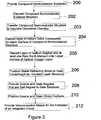
- FIG. 3is a simplified flow chart illustrating a method of manufacturing a self-aligned enhancement mode compound semiconductor MISFET in accordance with another preferred embodiment of the present invention.
- the exemplification set out hereinillustrates a preferred embodiment of the invention in one form thereof, and such exemplification is not intended to be construed as limiting in any manner.
- the present inventionprovides, among other things, a self-aligned enhancement mode metal-oxide-compound semiconductor FET and integrated circuit utilizing these FETs.
- the FETincludes an indium oxygen passivating+insulating structure that is comprised of at least two layers.
- the first layeris most preferably one monolayer in thickness or approximately 3 angstroms thick but preferably less that 25 angstroms in thickness and composed substantially of indium oxygen compounds including but not limited to stoichiometric In 2 O 3 , In 2 O, and possibly a lesser fraction of other indium oxygen compounds.
- the upper insulating layer in the gate insulating structureis composed of an insulator that does not intermix with the underlying indium gallium oxygen passivating structure.
- the upper layermust possess excellent insulating qualities, and is most typically composed of gallium oxygen and a third rare earth element
- the upper insulating layermay be comprised of gallium sulfur and a third rare earth element and that together form a ternary insulating material.
- the upper insulating layermay also be composed of gallium oxygen sulfur compounds with the addition of at least one rare earth element. Therefore the entire gate insulating structure is comprised of at least two layers where the lower layer directly adjacent to the compound semiconductor structure is comprised of indium gallium and oxygen and an upper layer comprised of at least two of the elements of indium, gallium, oxygen, sulfur, with the addition of at least one rare earth element.
- an intermediate graded layerthat is comprised of a fractional mixture of the lower and upper materials may also exist in the passivating and insulating structure for compound semiconductor structures.
- the initial indium oxygen layer, any intermediate graded layer and the top insulating regionform both a indium gallium oxide insulating structure and the gate insulator region of a metal-oxide-compound semiconductor field effect transistor.
- the initial indium oxygen layerforms an atomically abrupt interface with the top layer of the compound semiconductor wafer structure, and does not introduce midgap surface states into the compound semiconductor material.
- a refractory metal gate electrodeis preferably positioned on the upper surface of the gate insulator structure layer. The refractory metal is stable on the gate insulator structure layer at elevated temperature.
- the metal-oxide-sulfide-compound semiconductor transistorincludes multi-layer gate insulator structure including an initial indium, gallium oxygen layer, intermediate transition layer, and upper insulating layer of 30-250 angstroms in thickness positioned on upper surface of a compound semiconductor heterostructure that form the gate insulator structure.
- the preferred embodimentalso comprises a compound semiconductor heterostructure including a GaAs, Al x Ga 1 ⁇ x As and In y Ga 1 ⁇ y As layers with or without n-type and/or p-type charge supplying layers which are grown on a compound semiconductor substrate, a refractory metal gate of Pt, Ir, W, WN, or WSi, with or without self aligned donor (n-channel FET) or acceptor (p-channel FET) implants, and source and drain ohmic contacts.
- a compound semiconductor heterostructureincluding a GaAs, Al x Ga 1 ⁇ x As and In y Ga 1 ⁇ y As layers with or without n-type and/or p-type charge supplying layers which are grown on a compound semiconductor substrate, a refractory metal gate of Pt, Ir, W, WN, or WSi, with or without self aligned donor (n-channel FET) or acceptor (p-channel FET) implants, and source and drain ohmic contacts.
- the compound semiconductor heterostructurecomprises an In y Ga 1 ⁇ y As, Al x In 1 ⁇ x As, and InP compound semiconductor heterostructure and n-type and/or p-type charge supplying layers which are grown on an InP substrate, and a refractory metal gate of Pt, Ir, W, WN, or WSi, self aligned donor (n-channel FET) or acceptor (p-channel FET) implants, and source and drain ohmic contacts.
- the compound semiconductor heterostructurecomprises an GaN, Al y Ga 1 ⁇ y N, or In 1 ⁇ x Ga x N, Al y Ga 1 ⁇ y N compound semiconductor heterostructure and n-type and/or p-type charge supplying layers which are grown on an InP substrate, and a refractory metal gate of Pt, Ir, W, WN, or WSi, self aligned donor (n-channel FET) or acceptor (p-channel FET) implants, and source and drain ohmic contacts.
- the GaN/Al y Ga 1 ⁇ y N compound semiconductor structurepossess n-type charge in the channel of the structure that results from the piezoelectric strain in the compound semiconductor structure.
- FIG. 1is simplified cross sectional view of a self-aligned enhancement mode compound semiconductor MOSFET in accordance with a preferred embodiment of the present invention.
- Device 10includes a compound semiconductor material, such as any III-V material employed in any semiconductor device, represented herein by a Ill-V semiconductor or insulating substrate 11 and a compound semiconductor epitaxial layer structure 12 .
- the substrate 11 and any epitaxial layer structure 12 formed thereonwill be referred to simply as a compound semiconductor wafer structure which in FIG. 1 is designated 13 .
- Methods of fabricating semiconductor wafer structure 13include, but are not limited to, molecular beam epitaxy (MBE) and metal organic chemical vapor deposition (MOCVD), Chemical Beam Epitaxy (CBE) and the associated deposition techniques. It will of course be understood that in some specific applications, there may be no epitaxial layers present and upper surface of top layer 15 may simply be the upper surface of substrate 11 .
- Device 10further comprises a gate insulator structures ( 30 ) that includes at least two or more layers.
- the first layer of the gate insulator structure ( 31 )is composed entirely of indium oxide compounds and is directly adjacent to and deposited upon the compound semiconductor structure.
- the second layer of the gate insulator structure ( 32 )is composed of a compound of gallium, oxygen, and one or more rare earth elements, or gallium sulphur, and one or more rare earth elements from the periodic table.
- the initial indium oxygen layer ( 31 )forms an atomically abrupt interface 14 with the upper surface of top layer 15 , the top layer of the compound semiconductor structure.
- a refractory metal gate electrode 17 which is stable in the presence of top insulating material at elevated temperatureis positioned on upper surface 18 of the gate insulator structure.
- Dielectric spacers 26are positioned to cover the sidewalls of metal gate electrode 17 .
- Source and drain contacts 19 and 20are deposited on self-aligned source and drain areas 21 and 22 , respectively.
- the compound semiconductor epitaxial layer structureconsists of a ⁇ 11 angstrom GaAs top layer ( 15 ), a ⁇ 101 angstrom Al x Ga 1 ⁇ x As spacer layer ( 23 ), a ⁇ 251 angstrom In y Ga 1 ⁇ y As channel layer ( 24 ), and an Al x Ga 1 ⁇ x As buffer layer ( 25 ) grown on a GaAs substrate ( 11 ).
- Top GaAs layer ( 15 )is used to form an atomically abrupt layer with the gate insulator structure with an abrupt interface with low defect density.
- a III-V compound semiconductor wafer structure 13 with an atomically ordered pure and chemically clean upper surface of top layer 15is prepared in an ultra-high vacuum semiconductor growth chamber and transferred via a ultra high vacuum transfer chamber to a second ultra high vacuum oxide and insulator deposition chamber.
- the initial indium oxygen layer ( 31 )is deposited on upper compound semiconductor surface layer 15 using thermal evaporation from a high purity or vacuum deposition grade In 2 O 3 sources or indium gadolinium garnet, In 3 Gd 5 O 12 .
- This initial indium oxygen layeris deposited while holding the substrate temperature of the compound semiconductor structure at ⁇ 450° C., and more preferably at a substrate temperature ⁇ 405° C., and most preferably at a substrate temperature between 250° C. and 400° C.
- deposition of the second insulator layeris initiated.
- the deposition of the second insulator layerstarts by directing the flux from a low power oxygen plasma source into the ultra high vacuum system such that the molecular oxygen or oxygen plasma effluent and species are largely directed toward and impinging upon said compound semiconductor structure with initial gallium oxygen layer.
- the flux from the oxygen sourcethat may include molecular oxygen, atomic oxygen most typically produced with or without plasma, or some combination of molecular and atomic oxygen, should be directed at the surface for between 2-5 seconds, subsequently followed by the co-evaporation of gallium oxygen compounds from Ga 2 O 3 , indium oxygen compounds from In 2 O 3 , and a third thermal evaporation or e-beam source that contains a rare-earth element (e.g. Gd) or rare earth oxide compound (Gd 2 O 3 ).
- the flux beams from the oxygen source, In 2 O 3 , Ga 2 O 3 and rare-earth evaporation source thermal evaporation sourcesare carefully balanced to provide a ternary insulator layer on top of the initial indium oxygen layer on said compound semiconductor structure.
- the substrate temperatureis simultaneously adjusted to provide an optimized substrate temperature for the deposition of this layer.
- the substrate temperature required to deposit the gallium+oxygen+rare earth layeris ⁇ 510° C.
- this second insulating layeris comprised of gallium sulphur and at least and at least one rare earth element.
- this second insulating layeris comprised of gallium, oxygen, at least one rare earth element, and a fraction of indium adjusted to allow the layer to possess sufficient insulating properties.
- this second insulating layeris comprised of gallium, sulphur, at least one rare earth element, and an indium fraction adjusted to allow the layer to possess sufficient insulating properties.
- this second insulator layerproceeds until the total insulator thickness of 50-250 angstroms is achieved.
- Shutters and valvesare utilized to stop the deposition of the second insulting layer upon the deposition of the required thickness of the insulator layer.
- the substrate temperatureis cooled in-vacuum to approximately 200° C., and the deposition of a refractory metal which is stable and does not interdiffise with on the top layer of the gate insulator structure at elevated temperature such as Ir, Pt, WSi or WN is deposited on upper surface 18 of oxide layer 32 and subsequently patterned using standard lithography.
- the refractory metal layeris etched until oxide layer 31 is exposed using a refractory metal etching technique such as a fluorine based dry etching process.
- the refractory metal etching proceduredoes not etch the oxide layer 31 , thus, oxide layer 31 functions as an etch stop layer such that upper surface of top layer 15 remains protected by oxide layer 31 .
- All processing stepsare performed using low damage plasma processing.
- Self-aligned source and drain areas 21 and 22respectively are realized by lithography and possibly with or without ion implantation of Si (n-channel device) and Be/F or C/F (p-channel device) using the refractory metal gate electrode 17 and the dielectric spacers 26 as implantation masks.
- ion implantation schemesare compatible with standard processing of complementary compound semiconductor heterostructure FET technologies and are well known to those skilled in the art.
- ion implantation layersare not necessary for the formation of compound semiconductor MOSFETs if modulation doping or other doped layers are provided during the epitaxial growth of the compound semiconductor structure.
- the implants, if present in the device or circuit,are activated at 700-950° C. using rapid thermal annealing in an ultra high vacuum environment such that degradation of the interface 16 established between top layer 15 and oxide layer 31 is completely excluded.
- ohmic source and drain contacts 19 and 20are deposited on the self-aligned source and drain areas 21 and 22 , respectively.
- the devicesmay then be interconnected using the standard methods to those skilled in the art of integrated microelectronics and integrated circuit manufacture.
- FIG. 2is a simplified flow chart illustrating a method of manufacturing a self-aligned enhancement mode compound semiconductor MOSFET in accordance with a preferred embodiment of the present invention.
- a compound semiconductor wafer structureis produced using standard epitaxial growth methods in the art.
- a layer consisting of indium oxygen compounds including but not limited to In 2 O 3 and In 2 Ois deposited on upper surface of said compound semiconductor wafer structure.
- an insulating layer of gallium oxygen and one or more rare earth elementsis deposited on the upper surface of the initial gallium oxygen compound layer.
- the gallium oxide gate insulator structureis formed in steps 104 and 105 .
- a stable refractory gate metalis positioned on upper surface of said gate insulator structure.
- source and drain ion implantsare provided self-aligned to the gate electrode.
- source and drain ohmic contactsare positioned on ion implanted source and drain areas.
- step 100provides a compound semiconductor substrate such as GaAs, InP, or various GaN substrates including: GaN-on-Sapphire, GaN—AlN-on-Sapphire, GaN—AlN-on-SiC, GaN—AlN—C-Silicon, and GaN-on-GaN.
- Step 102includes the preparation and epitaxial growth of an atomically ordered and chemically clean upper surface of the compound semiconductor wafer structure.
- Step 103preferably comprises thermal evaporation from a purified and crystalline gadolinium gallium garnet or Ga 2 O 3 source on an atomically ordered and chemically clean upper surface of the compound semiconductor wafer structure.
- Step 104comprises the formation of a indium+gallium+oxygen+rare earth elemental insulating layer or a gallium+oxygen+rare earth insulating layer formed through the simultaneous vacuum evaporation of gallium oxygen species, indium oxygen species and at least one rare earth element such as gadolinium with the simultaneous oxidation using the effluent of an oxygen molecular oxygen or gas plasma source directed in simultaneous combination with other thermal evaporation sources toward substrate 100 .
- the initial indium gallium oxygen compound layer of the gate insulator structurepreferably functions as an etch stop layer such that the upper surface of the compound semiconductor wafer structure remains protected by the gate oxide during and after gate metal etching.
- the refractory gate metaldesirably does not react with or diffuse into the gate oxide layer during high temperature annealing of the self-aligned source and drain ion implants.
- the quality of the interface formed by the gate oxide layer and the upper surface of the compound semiconductor structureis desirably preserved during high temperature annealing of the self-aligned source and drain ion implants.
- the self-aligned source and drain implantsare desirably annealed at approximately 700-950° C. in an ultra high vacuum environment.
- the self-aligned source and drain implantsare desirably realized by positioning dielectric spacers on the sidewalls of the refractory gate metal.
- FIG. 3is a simplified flow chart illustrating a method of manufacturing a self-aligned enhancement mode compound semiconductor MISFET in accordance with another preferred embodiment of the present invention.
- a compound semiconductor wafer structureis produced using standard epitaxial growth methods in the art.
- a layer consisting of indium oxygen compounds including but not limited to In 2 O 3 and In 2 Oare deposited on upper surface of said compound semiconductor wafer structure.
- an insulating layer of gallium sulphur and one or more rare earth elementsis deposited on the upper surface of the initial gallium oxygen compound layer.
- the gallium oxide-sulphide gate insulator structureis formed in steps 204 and 205 .
- a stable refractory gate metalis positioned on upper surface of said gate insulator structure.
- source and drain regionsare self-aligned to the gate electrode.
- source and drain ohmic contactsare positioned source and drain areas that may or may not be formed using ion implantation.
- step 200provides a compound semiconductor substrate such as GaAs, InP, or various GaN substrates including: GaN-on-Sapphire, GaN—AlN-on-Sapphire, GaN—AlN-on-SiC, GaN—AlN—C-Silicon, and GaN-on-GaN.
- Step 202includes the preparation and epitaxial growth of an atomically ordered and chemically clean upper surface of the compound semiconductor wafer structure.
- Step 203preferably comprises thermal evaporation from a purified and crystalline gadolinium gallium garnet or Ga 2 O 3 source on an atomically ordered and chemically clean upper surface of the compound semiconductor wafer structure.
- Step 204comprises the formation of a indium+gallium+oxygen+rare earth elemental insulating layer or a gallium+oxygen+rare earth insulating layer formed through the simultaneous vacuum evaporation of gallium oxygen species, indium oxygen species and at least one rare earth element such as Gadolinium with the simultaneous oxidation using the effluent of an oxygen gas plasma source directed in simultaneous combination with other thermal evaporation sources toward substrate 200 .
- the initial indium gallium oxygen compound layer of the gate insulator structurepreferably functions as an etch stop layer such that the upper surface of the compound semiconductor wafer structure remains protected by the gate oxide during and after gate metal etching.
- the refractory gate metaldesirably does not react with or diffuse into the gate oxide layer during high temperature annealing of the self-aligned source and drain ion implants.
- the quality of the interface formed by the gate oxide layer and the upper surface of the compound semiconductor structureis desirably preserved during high temperature annealing of the self-aligned source and drain ion implants.
- the self-aligned source and drain implantsare desirably annealed at approximately 700-950° C. in an ultra high vacuum environment.
- the self-aligned source and drain implantsare desirably realized by positioning dielectric spacers on the sidewalls of the refractory gate metal.
- new and improved compound semiconductor devices and methods of fabricationare disclosed.
- the new and improved self-aligned enhancement mode metal-oxide-compound semiconductor heterostructure field effect transistorsenable stable and reliable device operation, provide optimum compound semiconductor device performance for low power/high performance complementary circuits and architectures, keep interconnection delay in VLSI and ULSI under control, and provide optimum efficiency and output power for RF and microwave applications as well as for digital integrated circuits that require very high integration densities.
Landscapes
- Insulated Gate Type Field-Effect Transistor (AREA)
- Thin Film Transistor (AREA)
Abstract
Description
- [0001] This invention was made with the support by the United States Government under US Army Aviation and Missile Command contract number DAAH01-02-C-R028. The United States may have certain rights to the invention.
- The present invention generally relates to low power and high speed integrated circuits in the compound semiconductor field utilizing field effect transistors and more specifically to enhancement mode self-aligned metal-oxide-compound semiconductor transistors, depletion mode self-aligned metal-oxide-compound semiconductor transistors, methods of materials growth and fabrication of these transistors, and the ultra large scale integration of said transistors forming integrated circuits.[0002]
- The main barrier to the realization of a desirable Complementary Metal Oxide Semiconductor (CMOS) technology in compound semiconductors is the absence of a proper gate insulator structure and gate passivation layer that passivates the surface of a compound semiconductor structure reducing the interface state trap density and simultaneously provides for sufficient insulating properties that are necessary for low gate leakage currents in the picoamp to nanoamp range required by very large scale (VLSI) and ultra large scale (ULSI) integrated circuit technology. Field effect transistor (FETs) widely used in the III-V semiconductor industry typically employ metal gates placed directly on the compound semiconductor structure forming Schottky gate contacts that are have quiescent-state leakage currents exceeding many microamps. The use of non-insulated metal gates placed directly onto compound semiconductor technology further results in individual transistors and integrated circuits that have excessively high power dissipation, reduced transconductance, low threshold voltage, reduced logic swing and the inability to operate on a single power supply, and generally limited performance characteristics. The high magnitude of the quiescent leakage current limits the maximum integration of GaAs, InP, and GaN based devices to circuits of several hundred thousand transistors.[0003]
- In contrast, conventional silicon technology has a very mature and useful complementary metal oxide semiconductor (CMOS) technology., In silicon CMOS technology an insulating layer may be formed at the silicon structure surface without the introduction or formation of an undue density of electronic traps in the combined silicon/SiO[0004]2semiconductor structure. Typically the trap density in the silicon/SiO2materials system observed before hydrogen passivation of any traps or defects is in the 1010-1011cm−2/eV at the center of the band gap. Thus, the insulating layer formed at the silicon wafer surface may act as a passivating layer that occupies dangling bonds at the silicon surface, reduces the interface state trap density in the energy gap and protects the semiconductor surface from environmental contamination, non-planar oxidation or reaction of impurities and the associated formation of electronic traps. It is well know by those skilled in the art that the electronic traps that are observed midway between the conduction band and valence band are caused by the disruption of the crystal symmetry at a semiconductor surface. Thus, excessive intermixing or disruption of the semiconductor surface at the interface between the semiconductor structure and any upper layer or layers will introduce increased electronics traps into the semiconductor structure.
- The simultaneous integration of many millions of transistors is possible at high integration densities using silicon CMOS technology. These ultra high integration densities and levels cannot be obtained using metal, Schottky-style gates that are not insulated from the compound semiconductor structure in compound semiconductor FETs. Thus Si CMOS technology offers significant advantages in terms of the low gate leakage of individual transistors, and circuit integration level and manufacturing cost.[0005]
- However when compared to silicon technology, compound semiconductors such as GaAs, InP, and GaN exhibit faster and more optimized speed/power performance and efficiency. The market acceptance of these GaAs, InP, and GaN integrated circuit technologies remains low because of high gate leakage in compound semiconductor MESFETS and MOSFETs, the lack of ability to demonstrate high integration densities with low amounts of operating power, and higher manufacturing cost. Thus, silicon CMOS dominates the field of low power high performance analog and digital integrated circuitry, and circuits based upon GaAs, InP, GaN technologies cannot successfully penetrate this market.[0006]
- What is needed is a compound semiconductor-passivation layer-insulator structure with an improved sharpness and abruptness at the semiconductor-passivation layer interface. What is needed are new and improved compound semiconductor field effect transistors (FET). What is needed is a compound semiconductor passivation layer that is conducting in a manner that allows the formation of a JFET-type junction adjacent to the channel. What is needed are p-type and n-type conducting passivation layers useful in JFET structure formation. What is needed are JFETs with a reduced gate leakage. What is also needed are new and improved compound semiconductor FETs using metal-oxide-semiconductor junctions (MOSFET). What is also needed are new and improved compound semiconductor MOSFETs using a self-aligned gate structure. What is also needed are new and improved self-aligned compound semiconductor MOSFETs using enhancement mode and depletion mode operation. What is also needed are new and improved self-aligned compound semiconductor MOSFETs with stable and reliable device operation. What is also needed are new and improved self-aligned compound semiconductor MOSFETs which enable optimum compound semiconductor device performance. What is also needed are new and improved self-aligned compound semiconductor MOSFETs with optimum efficiency and output power for RF and microwave applications. What is also needed are new and improved self-aligned compound semiconductor MOSFETs for use in complementary circuits and architectures. What is also needed are new and improved self-aligned compound semiconductor MOSFETs for low power/high performance complementary circuits and architectures. What is also needed are new and improved self-aligned compound semiconductor MOSFETs which offer the design flexibility of complementary architectures. What is also needed are new and improved self-aligned compound semiconductor MOSFETs which keep interconnection delays in ultra large scale integration under control. What is needed are new and useful complementary integrated circuits where each individual transistor has a leakage current approaching 10[0007]−12amp. What is needed is a truly useful integrated circuit technology for GaAs, InP, and GaN that allows for the useful and economical operation of ULSI digital integrated circuits in compound semiconductors. What is needed are new and improved compound semiconductor MOSFET integrated circuits with very low net power dissipation. What is needed are new and improved compound semiconductor MOSFET devices with low gate leakage currents that may be integrated together to form ultra large scale integrated circuits that include millions of transistors. What is needed are new and improved complementary MOSFET devices and circuits in compound semiconductors that allow the direct use, transfer and application of silicon CMOS design that already exits in the art.
- What is also needed are new and improved methods of fabrication of self-aligned compound semiconductor MOSFETs. What is also needed is new and improved methods of fabrication of self-aligned compound semiconductor MOSFETs that are compatible with established complementary GaAs heterostructure FETs technologies. What is also needed are new and improved compound semiconductor MOSFETs which are relatively easy to fabricate and use.[0008]
- A first aspect of the present invention generally relates to the interface between the compound semiconductor structure and the gate insulating structure. It is well known to those skilled in the art that for best results the abruptness of the interface between the compound semiconductor structure and the conductive passivating+insulating layer adjacent to the compound semiconductor structure should be reduced to one atomic layer in order to reduce the density of electronic traps in the resulting metal oxide semiconductor transistor device. If the interface between the compound semiconductor structure and the passivating and insulating layer varies by 3 or more atomic layers the electronic traps density will rise to levels that will cause the electrical behavior of the resulting transistor structure to be irreproducible due to charging and discharging of a large number of electronic traps. If the operation of a transistor is not reproducible as a function of voltage and current, the transistor is not useful. The abruptness of the interface between the compound semiconductor structure and the gate insulating structure may be improved by epitaxially growing the compound semiconductor structure before the oxide is deposited. A compound semiconductor structure with an atomically smooth upper surface is most desirable. The smoothness of a compound semiconductor growth during epitaxial growth processes such a Molecular Beam Epitaxy, Chemical Beam Epitaxy, Metal Organic Chemical Vapor Deposition, and related techniques may be improved by reducing the overall epitaxial growth rate while maintaining the substrate temperatures. For example in molecular beam epitaxy it is most common to produce compound semiconductor epitaxial layered structures at growth rates of between 2.0-3.5 angstroms per second. The interfaces produced by compound semiconductor epitaxial wafer growths that proceed at this rate and higher rates often lead to compound semiconductor surfaces that have a roughness of more than 3 atomic layers as observed by techniques such as Reflection High Energy Electron Diffraction (RHEED), atomic force microscopy, and scanning tunneling microscopy. Increased growth surface roughness have been observed in the RHEED features when the epitaxial layer growth proceeds at rates above 2.5 angstroms per second. By reducing the growth rate of GaAs and other compound semiconductors to below 1 angstrom per second for surface layers of compound semiconductor structures including GaAs, InP, GaN and other compound semiconductor semiconductors surface roughness may be reduced.[0009]
- A second aspect of the present invention generally relates to a gate insulating structure comprised of a multi-layer stack of indium and gallium containing oxides that includes indium oxide in the first passivating layer adjacent to the compound semiconductor structure and a second, third, fourth etc. insulating layer comprised of gallium, oxygen and at least one rare-earth element. A third aspect of the present invention generally relates to a gate insulating structure comprised of a multi-layer stack of indium and gallium containing oxides that include indium oxide in the first passivating layer adjacent to the compound semiconductor structure and second insulating layer comprised of gallium, sulphur, and at least one rare-earth element. A fourth aspect of this invention is that oxygen and sulphur may be used interchangably in the passivation and insulating layers placed upon the compound semiconductor structures where the other elements in the passivation and insulating layers layer remain fixed. A fifth aspect of the invention is to provide for a conducting passivation layer adjacent to the compound semiconductor structure that may possess either p-type of n-type conductivity allowing for the formation of a JFET structure utilizing n-type and p-type compound semiconductors respectively. The indium oxide compounds layer may further incorporate fractions of other elements that are able to allow the formation of the layers that are either p-type or n-type in conductivity. In addition the deposition conditions of the indium oxygen layers may be utilized to further establish the conductivity of the indium oxide layers as p-type and n-type. Parameters such as substrate temperature, oxygen overpressure, deposition rate, and the incorporation of other elements including tin may be adjusted to provide for different levels of p-type and n-type doping. Normally, an ultra high vacuum technique called molecular beam epitaxy or chemical beam epitaxy is used to form these gate insulating structures. During the epitaxial growth of such structures, interfacial smoothness may be monitored using an in-situ electron diffraction technique called Reflection High Energy Electron Diffraction (RHEED) to monitor the smoothness of the interface formed between the gate insulating structures and the compound semiconductor material. If the RHEED features are linearly sharp possessing a minimum of dots or discontinuous structure, those skilled in the art of RHEED would identify that the interface remains atomically smooth with a maximum abruptness during the deposition of oxide materials on the compound semiconductor structure. The RHEED features slowly disappear as the oxide deposition proceeds on the compound semiconductor structure showing that the materials pass from crystalline structure in the compound semiconductor, to oxide structure that has long range 2D order in the first 1-2 monolayers of oxide, to an amorphous-like structure as the deposition proceed for the next 25 angstroms, to an amorphous structure within 75 angstroms of total oxide structure growth. Previously, utilizing only Ga-oxides during deposition the RHEED pattern is observed to possess a discontinuous (i.e. non-streaky) pattern before its disappearance as the oxide thickness increases. During deposition of the initial indium, the same type of streaky RHEED pattern can be observed as in the case of Ga-oxide based passivation layers.[0010]
- A sixth aspect of the present invention generally relates to increased surface mobility of indium oxides on the epitaxial surface as compared to that of gallium oxides. Generally, species with higher surface mobilities at any given temperature may be deposited in a monolayer-by-monolayer manner at reduced substrate temperature. Thus, the increased surface mobility observed for indium oxide allows for deposition of good electrical quality in a wider temperature window than allowed by gallium oxide containing passivation layers.[0011]
- A seventh aspect of this invention generally relates to the use of indium oxide compounds for the manufacturing of a generally conductive interfaces between the top layers of the gate insulating structure and the compound semiconductor surface. The initial indium oxide passivation layer that forms the initial and lowest passivation layer of a gate insulating structure, without eliminating the nominally insulating/semiconducting properties of the gallium oxide+one rare earth layer deposited upon the initial indium oxide layer adjacent to the compound semiconductor structure surface.[0012]
- A eight aspect of the present invention generally relates to a method for improving the smoothness of the surface of the compound semiconductor structure by incorporating interruptions in the epitaxial growth under ultra high vacuum conditions, and then initiate growth by alternately exposing the surface of the compound semiconductor to ½ monolayers of a group III element (i.e. Ga, In, Al, Tl) followed by the exposure of ½ a monolayer of a group V element (i.e. As, P, Sb, N) for the case of III-V compound semiconductor structures. This aspect of compound semiconductor growth is referred to as migration enhanced epitaxy and is used by those skilled in compound semiconductor growth techniques of Molecular Beam Epitaxy, Chemical Beam Epitaxy, Metal Organic Chemical Vapor Deposition and the related epitaxial growth techniques.[0013]
- A ninth aspect of the invention is that a p-n junction may be formed between the top layer of the compound semiconductor structure and the first layer of the gate insulator structure. An example of this embodiment would be the use of an InGaAs channel in the compound semiconductor structure that transports current using electrons, while depositing a p-type indium oxide layer on top of the compound semiconductor layer. Similarly, a p-channel compound semiconductor channel and an n-type passivating+insulating structure would form a junction field effect transistor structure as well.[0014]
- There has thus been outlined features of the invention in order that the detailed description thereof that follows may be better understood, and in order that the present contribution to the art may be better appreciated. There are, of course, additional features of the invention that will form the subject matter of the claims appended hereto. In this respect, before explaining at least one embodiment of the invention in detail, it is to be understood that the invention is not limited in its application to the details of construction and to the arrangements of the components set forth above or in the following description or illustrated in the drawings. The invention is capable of other embodiments and of being practiced and carried out in various ways. Also, it is to be understood that the phraseology and terminology employed herein are for the purpose of description and should not be regarded as limiting. As such, those skilled in the art will appreciate that the conception, upon which this disclosure is based, may readily be utilized as a basis for the designing of other structures, methods and systems for carrying out the several purposes of the present invention. It is important, therefore, that the claims be regarded as including such equivalent constructions insofar as they do not depart from the spirit and scope of the present invention.[0015]
- A more complete understanding of the present invention may be derived by referring to the detailed description and claims when considered in connection with the figures, wherein like reference numbers refer to similar items throughout the figures, and:[0016]
- FIG. 1 is a simplified cross sectional view of a self-aligned enhancement mode compound semiconductor MOSFET in accordance with a preferred embodiment of the present invention;[0017]
- FIG. 2 is a simplified flow chart illustrating a method of manufacturing a self-aligned enhancement mode compound semiconductor MOSFET in accordance with a preferred embodiment of the present invention. The exemplification set out herein illustrates a preferred embodiment of the invention in one form thereof, and such exemplification is not intended to be construed as limiting in any manner.[0018]
- FIG. 3 is a simplified flow chart illustrating a method of manufacturing a self-aligned enhancement mode compound semiconductor MISFET in accordance with another preferred embodiment of the present invention. The exemplification set out herein illustrates a preferred embodiment of the invention in one form thereof, and such exemplification is not intended to be construed as limiting in any manner.[0019]
- The present invention provides, among other things, a self-aligned enhancement mode metal-oxide-compound semiconductor FET and integrated circuit utilizing these FETs. The FET includes an indium oxygen passivating+insulating structure that is comprised of at least two layers. The first layer is most preferably one monolayer in thickness or approximately 3 angstroms thick but preferably less that 25 angstroms in thickness and composed substantially of indium oxygen compounds including but not limited to stoichiometric In[0020]2O3, In2O, and possibly a lesser fraction of other indium oxygen compounds. The upper insulating layer in the gate insulating structure is composed of an insulator that does not intermix with the underlying indium gallium oxygen passivating structure. This upper layer must possess excellent insulating qualities, and is most typically composed of gallium oxygen and a third rare earth element Alternatively, the upper insulating layer may be comprised of gallium sulfur and a third rare earth element and that together form a ternary insulating material. In another embodiment the upper insulating layer may also be composed of gallium oxygen sulfur compounds with the addition of at least one rare earth element. Therefore the entire gate insulating structure is comprised of at least two layers where the lower layer directly adjacent to the compound semiconductor structure is comprised of indium gallium and oxygen and an upper layer comprised of at least two of the elements of indium, gallium, oxygen, sulfur, with the addition of at least one rare earth element. In addition an intermediate graded layer that is comprised of a fractional mixture of the lower and upper materials may also exist in the passivating and insulating structure for compound semiconductor structures. Together the initial indium oxygen layer, any intermediate graded layer and the top insulating region form both a indium gallium oxide insulating structure and the gate insulator region of a metal-oxide-compound semiconductor field effect transistor. The initial indium oxygen layer forms an atomically abrupt interface with the top layer of the compound semiconductor wafer structure, and does not introduce midgap surface states into the compound semiconductor material. A refractory metal gate electrode is preferably positioned on the upper surface of the gate insulator structure layer. The refractory metal is stable on the gate insulator structure layer at elevated temperature. Refractory metals with lower work functions such as iridium and platinum are most suitable for the formation of enhancement mode transistor devices in this metal oxide semiconductor transistor technology. Self-aligned source and drain areas, and source and drain contacts are positioned on the source and drain areas. In all embodiments preferred and otherwise, the metal-oxide-sulfide-compound semiconductor transistor includes multi-layer gate insulator structure including an initial indium, gallium oxygen layer, intermediate transition layer, and upper insulating layer of 30-250 angstroms in thickness positioned on upper surface of a compound semiconductor heterostructure that form the gate insulator structure. The preferred embodiment also comprises a compound semiconductor heterostructure including a GaAs, AlxGa1−xAs and InyGa1−yAs layers with or without n-type and/or p-type charge supplying layers which are grown on a compound semiconductor substrate, a refractory metal gate of Pt, Ir, W, WN, or WSi, with or without self aligned donor (n-channel FET) or acceptor (p-channel FET) implants, and source and drain ohmic contacts. In another preferred embodiment, the compound semiconductor heterostructure comprises an InyGa1−yAs, AlxIn1−xAs, and InP compound semiconductor heterostructure and n-type and/or p-type charge supplying layers which are grown on an InP substrate, and a refractory metal gate of Pt, Ir, W, WN, or WSi, self aligned donor (n-channel FET) or acceptor (p-channel FET) implants, and source and drain ohmic contacts. In another preferred embodiment the compound semiconductor heterostructure comprises an GaN, AlyGa1−yN, or In1−xGaxN, AlyGa1−yN compound semiconductor heterostructure and n-type and/or p-type charge supplying layers which are grown on an InP substrate, and a refractory metal gate of Pt, Ir, W, WN, or WSi, self aligned donor (n-channel FET) or acceptor (p-channel FET) implants, and source and drain ohmic contacts. In another preferred embodiment the GaN/AlyGa1−yN compound semiconductor structure possess n-type charge in the channel of the structure that results from the piezoelectric strain in the compound semiconductor structure.
- FIG. 1 is simplified cross sectional view of a self-aligned enhancement mode compound semiconductor MOSFET in accordance with a preferred embodiment of the present invention.[0021]
Device 10 includes a compound semiconductor material, such as any III-V material employed in any semiconductor device, represented herein by a Ill-V semiconductor or insulatingsubstrate 11 and a compound semiconductorepitaxial layer structure 12. For the purpose of this disclosure, thesubstrate 11 and anyepitaxial layer structure 12 formed thereon will be referred to simply as a compound semiconductor wafer structure which in FIG. 1 is designated13. Methods of fabricatingsemiconductor wafer structure 13 include, but are not limited to, molecular beam epitaxy (MBE) and metal organic chemical vapor deposition (MOCVD), Chemical Beam Epitaxy (CBE) and the associated deposition techniques. It will of course be understood that in some specific applications, there may be no epitaxial layers present and upper surface oftop layer 15 may simply be the upper surface ofsubstrate 11. - [0022]
Device 10 further comprises a gate insulator structures (30) that includes at least two or more layers. The first layer of the gate insulator structure (31) is composed entirely of indium oxide compounds and is directly adjacent to and deposited upon the compound semiconductor structure. The second layer of the gate insulator structure (32) is composed of a compound of gallium, oxygen, and one or more rare earth elements, or gallium sulphur, and one or more rare earth elements from the periodic table. The initial indium oxygen layer (31) forms an atomicallyabrupt interface 14 with the upper surface oftop layer 15, the top layer of the compound semiconductor structure. A refractorymetal gate electrode 17 which is stable in the presence of top insulating material at elevated temperature is positioned onupper surface 18 of the gate insulator structure.Dielectric spacers 26 are positioned to cover the sidewalls ofmetal gate electrode 17. Source anddrain contacts areas - In a specific embodiment, the compound semiconductor epitaxial layer structure consists of a <11 angstrom GaAs top layer ([0023]15), a <101 angstrom AlxGa1−xAs spacer layer (23), a <251 angstrom InyGa1−yAs channel layer (24), and an AlxGa1−xAs buffer layer (25) grown on a GaAs substrate (11). Top GaAs layer (15) is used to form an atomically abrupt layer with the gate insulator structure with an abrupt interface with low defect density.
- As a simplified example of fabricating a self-aligned enhancement mode compound semiconductor MOSFET in accordance with a preferred embodiment of the present invention, a III-V compound[0024]
semiconductor wafer structure 13 with an atomically ordered pure and chemically clean upper surface oftop layer 15 is prepared in an ultra-high vacuum semiconductor growth chamber and transferred via a ultra high vacuum transfer chamber to a second ultra high vacuum oxide and insulator deposition chamber. The initial indium oxygen layer (31) is deposited on upper compoundsemiconductor surface layer 15 using thermal evaporation from a high purity or vacuum deposition grade In2O3sources or indium gadolinium garnet, In3Gd5O12. This initial indium oxygen layer is deposited while holding the substrate temperature of the compound semiconductor structure at <450° C., and more preferably at a substrate temperature<405° C., and most preferably at a substrate temperature between 250° C. and 400° C. After the deposition of approximately 3 angstroms of indium oxygen compounds in the insulator deposition chamber over a 2 to 5 minute period of time, deposition of the second insulator layer is initiated. The deposition of the second insulator layer starts by directing the flux from a low power oxygen plasma source into the ultra high vacuum system such that the molecular oxygen or oxygen plasma effluent and species are largely directed toward and impinging upon said compound semiconductor structure with initial gallium oxygen layer. The flux from the oxygen source that may include molecular oxygen, atomic oxygen most typically produced with or without plasma, or some combination of molecular and atomic oxygen, should be directed at the surface for between 2-5 seconds, subsequently followed by the co-evaporation of gallium oxygen compounds from Ga2O3, indium oxygen compounds from In2O3, and a third thermal evaporation or e-beam source that contains a rare-earth element (e.g. Gd) or rare earth oxide compound (Gd2O3). The flux beams from the oxygen source, In2O3, Ga2O3and rare-earth evaporation source thermal evaporation sources are carefully balanced to provide a ternary insulator layer on top of the initial indium oxygen layer on said compound semiconductor structure. As the deposition of the second insulator layer is initiated, the substrate temperature is simultaneously adjusted to provide an optimized substrate temperature for the deposition of this layer. In this example the substrate temperature required to deposit the gallium+oxygen+rare earth layer is <510° C. In another preferred embodiment this second insulating layer is comprised of gallium sulphur and at least and at least one rare earth element. In yet another preferred embodiment, this second insulating layer is comprised of gallium, oxygen, at least one rare earth element, and a fraction of indium adjusted to allow the layer to possess sufficient insulating properties. In yet another preferred embodiment, this second insulating layer is comprised of gallium, sulphur, at least one rare earth element, and an indium fraction adjusted to allow the layer to possess sufficient insulating properties. The deposition of this second insulator layer proceeds until the total insulator thickness of 50-250 angstroms is achieved. Shutters and valves are utilized to stop the deposition of the second insulting layer upon the deposition of the required thickness of the insulator layer. The substrate temperature is cooled in-vacuum to approximately 200° C., and the deposition of a refractory metal which is stable and does not interdiffise with on the top layer of the gate insulator structure at elevated temperature such as Ir, Pt, WSi or WN is deposited onupper surface 18 ofoxide layer 32 and subsequently patterned using standard lithography. The refractory metal layer is etched untiloxide layer 31 is exposed using a refractory metal etching technique such as a fluorine based dry etching process. The refractory metal etching procedure does not etch theoxide layer 31, thus,oxide layer 31 functions as an etch stop layer such that upper surface oftop layer 15 remains protected byoxide layer 31. All processing steps are performed using low damage plasma processing. Self-aligned source and drainareas metal gate electrode 17 and thedielectric spacers 26 as implantation masks. Such ion implantation schemes are compatible with standard processing of complementary compound semiconductor heterostructure FET technologies and are well known to those skilled in the art. In addition, ion implantation layers are not necessary for the formation of compound semiconductor MOSFETs if modulation doping or other doped layers are provided during the epitaxial growth of the compound semiconductor structure. The implants, if present in the device or circuit, are activated at 700-950° C. using rapid thermal annealing in an ultra high vacuum environment such that degradation of the interface16 established betweentop layer 15 andoxide layer 31 is completely excluded. Finally, ohmic source anddrain contacts areas - FIG. 2 is a simplified flow chart illustrating a method of manufacturing a self-aligned enhancement mode compound semiconductor MOSFET in accordance with a preferred embodiment of the present invention. In[0025]
step 102, a compound semiconductor wafer structure is produced using standard epitaxial growth methods in the art. Instep 103, a layer consisting of indium oxygen compounds including but not limited to In2O3and In2O, is deposited on upper surface of said compound semiconductor wafer structure. Instep 104, an insulating layer of gallium oxygen and one or more rare earth elements is deposited on the upper surface of the initial gallium oxygen compound layer. The gallium oxide gate insulator structure is formed insteps step 106, a stable refractory gate metal is positioned on upper surface of said gate insulator structure. Instep 108, source and drain ion implants are provided self-aligned to the gate electrode. Instep 110, source and drain ohmic contacts are positioned on ion implanted source and drain areas. - In a preferred embodiment,[0026]
step 100 provides a compound semiconductor substrate such as GaAs, InP, or various GaN substrates including: GaN-on-Sapphire, GaN—AlN-on-Sapphire, GaN—AlN-on-SiC, GaN—AlN—C-Silicon, and GaN-on-GaN. Step102 includes the preparation and epitaxial growth of an atomically ordered and chemically clean upper surface of the compound semiconductor wafer structure. Step103 preferably comprises thermal evaporation from a purified and crystalline gadolinium gallium garnet or Ga2O3source on an atomically ordered and chemically clean upper surface of the compound semiconductor wafer structure. Step104 comprises the formation of a indium+gallium+oxygen+rare earth elemental insulating layer or a gallium+oxygen+rare earth insulating layer formed through the simultaneous vacuum evaporation of gallium oxygen species, indium oxygen species and at least one rare earth element such as gadolinium with the simultaneous oxidation using the effluent of an oxygen molecular oxygen or gas plasma source directed in simultaneous combination with other thermal evaporation sources towardsubstrate 100. The initial indium gallium oxygen compound layer of the gate insulator structure preferably functions as an etch stop layer such that the upper surface of the compound semiconductor wafer structure remains protected by the gate oxide during and after gate metal etching. The refractory gate metal desirably does not react with or diffuse into the gate oxide layer during high temperature annealing of the self-aligned source and drain ion implants. The quality of the interface formed by the gate oxide layer and the upper surface of the compound semiconductor structure is desirably preserved during high temperature annealing of the self-aligned source and drain ion implants. The self-aligned source and drain implants are desirably annealed at approximately 700-950° C. in an ultra high vacuum environment. The self-aligned source and drain implants are desirably realized by positioning dielectric spacers on the sidewalls of the refractory gate metal. - FIG. 3 is a simplified flow chart illustrating a method of manufacturing a self-aligned enhancement mode compound semiconductor MISFET in accordance with another preferred embodiment of the present invention. In[0027]
step 202, a compound semiconductor wafer structure is produced using standard epitaxial growth methods in the art. Instep 203, a layer consisting of indium oxygen compounds including but not limited to In2O3and In2O are deposited on upper surface of said compound semiconductor wafer structure. Instep 204, an insulating layer of gallium sulphur and one or more rare earth elements is deposited on the upper surface of the initial gallium oxygen compound layer. The gallium oxide-sulphide gate insulator structure is formed insteps step 206, a stable refractory gate metal is positioned on upper surface of said gate insulator structure. Instep 208, source and drain regions are self-aligned to the gate electrode. Instep 210, source and drain ohmic contacts are positioned source and drain areas that may or may not be formed using ion implantation. - In a preferred embodiment,[0028]
step 200 provides a compound semiconductor substrate such as GaAs, InP, or various GaN substrates including: GaN-on-Sapphire, GaN—AlN-on-Sapphire, GaN—AlN-on-SiC, GaN—AlN—C-Silicon, and GaN-on-GaN. Step202 includes the preparation and epitaxial growth of an atomically ordered and chemically clean upper surface of the compound semiconductor wafer structure. Step203 preferably comprises thermal evaporation from a purified and crystalline gadolinium gallium garnet or Ga2O3source on an atomically ordered and chemically clean upper surface of the compound semiconductor wafer structure. Step204 comprises the formation of a indium+gallium+oxygen+rare earth elemental insulating layer or a gallium+oxygen+rare earth insulating layer formed through the simultaneous vacuum evaporation of gallium oxygen species, indium oxygen species and at least one rare earth element such as Gadolinium with the simultaneous oxidation using the effluent of an oxygen gas plasma source directed in simultaneous combination with other thermal evaporation sources towardsubstrate 200. The initial indium gallium oxygen compound layer of the gate insulator structure preferably functions as an etch stop layer such that the upper surface of the compound semiconductor wafer structure remains protected by the gate oxide during and after gate metal etching. The refractory gate metal desirably does not react with or diffuse into the gate oxide layer during high temperature annealing of the self-aligned source and drain ion implants. The quality of the interface formed by the gate oxide layer and the upper surface of the compound semiconductor structure is desirably preserved during high temperature annealing of the self-aligned source and drain ion implants. The self-aligned source and drain implants are desirably annealed at approximately 700-950° C. in an ultra high vacuum environment. The self-aligned source and drain implants are desirably realized by positioning dielectric spacers on the sidewalls of the refractory gate metal. - It will now be understood that what has been disclosed herein includes new compound semiconductor devices and methods of fabrication. Those having skill in the art to which the present invention relates will now as a result of the teaching herein perceive various modifications. Accordingly, all such modifications are deemed to be within the scope of the invention that is to be limited only by the claims.[0029]
- Thus, new and improved compound semiconductor devices and methods of fabrication are disclosed. The new and improved self-aligned enhancement mode metal-oxide-compound semiconductor heterostructure field effect transistors enable stable and reliable device operation, provide optimum compound semiconductor device performance for low power/high performance complementary circuits and architectures, keep interconnection delay in VLSI and ULSI under control, and provide optimum efficiency and output power for RF and microwave applications as well as for digital integrated circuits that require very high integration densities.[0030]
- These improvements essentially solve or overcome the problems of the prior art, such as high gate leakage in compound semiconductor FET devices, low integration densities, dc electrical instability, and electrical hysteresis, and therefore provide a highly useful invention. While we have shown and described specific embodiments of the present invention, further modifications and improvements will occur to those skilled in the art. We desire it to be understood, therefore, that this invention is not limited to the particular forms shown and we intend in the appended claims to cover all modifications that do not depart from the spirit and scope of this invention.[0031]
Claims (137)
1. A metal-oxide-compound semiconductor field effect transistor comprising:
a compound semiconductor wafer structure having an upper surface;
a gate insulator structure comprising a first layer and a second layer;
said first layer substantially comprising compounds of indium and oxygen;
said second layer comprising compounds of gallium and oxygen and at least one rare earth element;
a gate electrode positioned on said gate insulator structure;
source and drain regions self-aligned to said gate electrode;
source and drain ohmic contacts positioned on said source and drain regions; and
wherein said gate electrode comprises a metal selected from the group consisting of Pt, Ir, W, WN, TiWN, WSi and combinations thereof.
2. The transistor ofclaim 1 wherein said first layer forms an atomically abrupt interface with said upper surface.
3. The transistor ofclaim 1 wherein said gate insulator structure is composed of at least three layers, including a graded layer that contains varying compositions of indium, gallium, oxygen and at least one rare-earth element.
4. The transistor ofclaim 3 wherein said gate insulator structure further comprises a third layer containing indium, gallium, and oxygen.
5. The transistor ofclaim 1 wherein said field effect transistor is an enhancement mode transistor.
6. The transistor ofclaim 1 wherein said field effect transistor is a depletion mode transistor.
7. The transistor ofclaim 1 wherein said first layer has a thickness of more than 3 angstroms and less than 25 angstroms.
8. The transistor ofclaim 1 wherein said gate insulator structure has a thickness of 20-300 angstroms.
9. The transistor ofclaim 1 wherein said first layer forms an interface with said upper surface that extends less than four atomic layers in depth of structural interface modulation.
10. The transistor ofclaim 1 wherein said first layer and said gate insulator structure protects said upper surface.
11. The transistor ofclaim 1 wherein said gate electrode comprises a refractory metal which is stable in the presence of the top layer of the gate insulator structure at 700° C.
12. The transistor ofclaim 1 wherein said source and drain regions are ion implanted to provide for one of an n-type or p-type region.
13. The transistor ofclaim 1 wherein said source and drain regions provide one of an n-channel or p-channel.
14. The transistor ofclaim 1 wherein said source and drain implants comprise at least one of Be, Si, Te, Sn, C, and Mg.
15. The transistor ofclaim 1 wherein said upper surface comprises GaAs.
16. The transistor ofclaim 1 wherein said upper surface comprises InxGa1−xAs.
17. The transistor ofclaim 1 wherein said upper surface comprises AlxGa1−xAs.
18. The transistor ofclaim 1 wherein said upper surface comprises GaN.
19. The transistor ofclaim 1 wherein said upper surface comprises InxGa1−xN.
20. The transistor ofclaim 1 wherein said upper surface comprises AlxGa1−xN.
21. The transistor ofclaim 1 wherein said upper surface comprises InzGa1−zSb.
22. A metal-oxide-compound semiconductor field effect transistor comprising:
a compound semiconductor wafer structure having an upper surface;
a gate insulator structure on said upper surface, said gate insulator structure comprising a first layer, a second layer, and a third layer;
said first layer substantially comprising compounds of indium and oxygen
said second layer comprising compounds of indium gallium and oxygen and at least one rare earth element;
said third layer above said second layer, said third layer substantially comprising gallium oxygen and at least one rare earth element, said third layer being insulating;
a gate electrode positioned on said gate insulator structure;
source and drain regions self-aligned to said gate electrode; and
source and drain ohmic contacts positioned on ion implanted source and drain areas;
wherein gate electrode comprises a metal selected from the group of Pt, Ir, W, WN, TiWN, WSi and combinations thereof.
23. The transistor ofclaim 22 wherein said first layer forms an atomically abrupt interface with said upper surface.
24. The transistor ofclaim 22 wherein said gate insulator structure is composed of at least three layers, including a graded layer that contains varying compositions of indium, gallium, oxygen and at least one rare-earth element.
25. The transistor ofclaim 22 wherein said gate insulator structure further comprises a third layer containing indium, gallium, and oxygen.
26. The transistor ofclaim 22 wherein said field effect transistor is an enhancement mode transistor.
27. The transistor ofclaim 22 wherein said field effect transistor is a depletion mode transistor.
28. The transistor ofclaim 22 wherein said first layer has a thickness of more than 3 angstroms and less than 25 angstroms.
29. The transistor ofclaim 22 wherein said gate insulator structure has a thickness of 20-300 angstroms.
30. The transistor ofclaim 22 wherein said first layer forms an interface with said upper surface that extends less than four atomic layers in depth of structural interface modulation.
31. The transistor ofclaim 22 wherein said first layer and said gate insulator structure protects said upper surface.
32. The transistor ofclaim 22 wherein said gate electrode comprises a refractory metal which is stable in the presence of the top layer of the gate insulator structure at 700° C.
33. The transistor ofclaim 22 wherein said source and drain regions are ion implanted to provide for one of an n-type or p-type region.
34. The transistor ofclaim 22 wherein said source and drain regions provide one of an n-channel or p-channel.
35. The transistor ofclaim 22 wherein said source and drain implants comprise at least one of Be, Si, Te, Sn, C, and Mg.
36. The transistor ofclaim 22 wherein said upper surface comprises GaAs.
37. The transistor ofclaim 22 wherein said upper surface comprises InxGa1−xAs.
38. The transistor ofclaim 22 wherein said upper surface comprises AlxGa1−xAs.
39. The transistor ofclaim 22 wherein said upper surface comprises GaN.
40. The transistor ofclaim 22 wherein said upper surface comprises InxGa1−xN.
41. The transistor ofclaim 22 wherein said upper surface comprises AlxGa1−xN.
42. The transistor ofclaim 22 wherein said upper surface comprises InzGa1−zSb.
43. A metal-oxide-compound semiconductor field effect transistor comprising:
a compound semiconductor wafer structure having an upper surface;
a multilayer gate insulator structure on said upper surface, said multilayer gate insulator structure substantially comprising alternating layers each of which comprise indium, gallium, oxygen, and at least one rare earth element.
a gate electrode positioned on said gate insulator structure;
source and drain regions self-aligned to said gate electrode; and
source and drain ohmic contacts positioned on ion implanted source and drain areas;
wherein gate electrode comprises a metal selected from the group of Pt, Ir, W, WN, TiWN, WSi and combinations thereof.
44. A metal-oxide-compound semiconductor field effect transistor comprising:
a compound semiconductor wafer structure having an upper surface;
a gate insulator structure positioned on upper surface of said compound semiconductor wafer structure;
a gate electrode positioned on said gate insulator structure;
source and drain regions self-aligned to said gate electrode; and
source and drain ohmic contacts positioned on ion implanted source and drain areas;
wherein said compound semiconductor structure comprises an AlxGa1−xAs, InyGa1−yAs, AlvIn1−vAs InP, InzGa1−zP, AlxGa1−xN, InyGa1−yN, GaN layer, said layer being positioned on said upper surface; a substrate on which resides said compound semiconductor wafer structure; and wherein said substrate includes an InP or GaN based semiconductor wafer.
45. A complementary metal-oxide compound semiconductor integrated circuit comprising an enhancement mode metal-oxide-compound semiconductor field effect transistor, said transistor comprising;
a compound semiconductor wafer structure having an upper surface;
a gate insulator structure positioned on said upper surface;
a gate electrode positioned on said upper surface;
source and drain self-aligned to the gate electrode; and source and drain ohmic contacts positioned on source and drain areas, wherein the compound semiconductor wafer structure comprises a wider band gap spacer layer and a narrower band gap channel layer;
wherein the narrower band gap channel layer comprises InyGa1−yAs; and wherein said transistor is integrated together with similar or complementary transistor devices to form complementary metal-oxide compound semiconductor integrated circuit
46. A metal-oxide-compound semiconductor field effect transistor comprising:
a compound semiconductor wafer structure having an upper surface;
a gate insulator structure comprising a first and second layer; said gate insulator on said upper surface;
said first layer substantially comprising compounds of indium and oxygen
said second layer comprising compounds of gallium and oxygen and at least one rare earth element;
a gate electrode positioned on said gate insulator structure.
47. A structure ofclaim 46 wherein said gate electrode comprises a refractory metal.
48. A structure ofclaim 46 wherein said gate electrode comprises a member of the group Pt, Ir, W, WN, TiWN, WSi, and combinations thereof.
49. A structure ofclaim 46 wherein said gate insulator structure further comprises a third layer.
50. A structure ofclaim 46 wherein compounds of said third layer comprising gallium and oxygen further comprise a rare earth element.
51. A structure ofclaim 50 wherein a composition of said third layer varies monotonically with depth in said third layer.
52. The structure ofclaim 50 wherein said gate insulator structure further comprises a fourth layer.
53. The structure ofclaim 46 wherein compounds of said fourth layer comprising gallium and oxygen.
54. A structure ofclaim 46 wherein compounds of said fourth layer comprising gallium and oxygen and further comprising a rare earth element.
55. A structure ofclaim 46 wherein compounds of said fourth layer comprising gallium oxygen and one rare earth and further comprising indium.
56. The structure ofclaim 46 wherein said first layer is adjacent and in contact with said upper surface.
57. The structure ofclaim 46 wherein said source and drain contacts are ion implanted.
58. The structure ofclaim 46 wherein said source and drain contacts are annealed in an ultra high vacuum environment.
59. The structure ofclaim 46 wherein said gate insulator structure passivates said upper surface.
60. A method for forming a metal-oxide-compound semiconductor field effect transistor, comprising:
providing a compound semiconductor wafer structure having an upper surface;
depositing a gate insulator structure comprising depositing a first layer and depositing a second layer, said gate insulator on said upper surface;
said first layer substantially comprising compounds of indium, gallium, and oxygen;
said second layer comprising at least one compound of gallium, oxygen and at least one rare earth element; and depositing a gate electrode positioned on said gate insulator structure.
61. The method ofclaim 60 comprising rapid thermal annealing said structure in a UHV environment.
62. The method ofclaim 58 wherein said rapid thermal annealing comprising annealing between 700 and 950 degrees Centigrade.
63. A metal-oxide-compound semiconductor field effect transistor comprising:
a compound semiconductor wafer structure having an upper surface;
a gate insulator structure comprising a first and second layer;
said first layer substantially comprising compounds of indium and oxygen
said second layer comprising compounds of gallium and sulphur and at least one rare earth element;
a gate electrode positioned on said gate insulator structure;
source and drain regions self-aligned to said gate electrode; and
source and drain ohmic contacts positioned on ion implanted source and drain areas;
wherein gate electrode comprises a metal selected from the group of Pt, Ir, W, WN, TiWN, WSi and combinations thereof.
64. The transistor ofclaim 63 wherein said first layer forms an atomically abrupt interface with said upper surface.
65. The transistor ofclaim 63 wherein said gate insulator structure is composed of at least three layers, including a graded layer that contains varying compositions of indium, gallium, oxygen and at least one rare-earth element.
66. The transistor ofclaim 65 wherein said gate insulator structure further comprises a third layer containing indium, gallium, and sulphur.
67. The transistor ofclaim 63 wherein said field effect transistor is an enhancement mode transistor.
68. The transistor ofclaim 63 wherein said field effect transistor is a depletion mode transistor.
69. The transistor ofclaim 63 wherein said first layer has a thickness of more than 3 angstroms and less than 25 angstroms.
70. The transistor ofclaim 63 wherein said gate insulator structure has a thickness of 20-300 angstroms.
71. The transistor ofclaim 63 wherein said first layer forms an interface with said upper surface that extends less than four atomic layers in depth of structural interface modulation.
72. The transistor ofclaim 63 wherein said first layer and said gate insulator structure protects said upper surface.
73. The transistor ofclaim 63 wherein said gate electrode comprises a refractory metal which is stable in the presence of the top layer of the gate insulator structure at 700° C.
74. The transistor ofclaim 63 wherein said source and drain regions are ion implanted to provide for one of an n-type or p-type region.
75. The transistor ofclaim 63 wherein said source and drain regions provide one of an n-channel or p-channel.
76. The transistor ofclaim 63 wherein said source and drain implants comprise at least one of Be, Si, Te, Sn, C, and Mg.
77. The transistor ofclaim 63 wherein said upper surface comprises GaAs.
78. The transistor ofclaim 63 wherein said upper surface comprises InxGa1−xAs.
79. The transistor ofclaim 63 wherein said upper surface comprises AlxGa1−xAs.
80. The transistor ofclaim 63 wherein said upper surface comprises GaN.
81. The transistor ofclaim 63 wherein said upper surface comprises InxGa1−xN.
82. The transistor ofclaim 63 wherein said upper surface comprises AlxGa1−xN.
83. The transistor ofclaim 63 wherein said upper surface comprises InzGa1−zSb.
84. A metal-oxide-compound semiconductor field effect transistor comprising:
a compound semiconductor wafer structure having an upper surface;
a gate insulator structure on said upper surface, said gate insulator structure comprising a first layer, a second layer, and a third layer;
said first layer substantially comprising compounds of indium and oxygen
said second layer comprising compounds of indium gallium oxygen and sulphur and at least one rare earth element;
said third layer above said second layer, said third layer substantially comprising gallium sulphur and at least one rare earth element, said third layer being insulating;
a gate electrode positioned on said gate insulator structure;
source and drain regions self-aligned to said gate electrode; and
source and drain ohmic contacts positioned on ion implanted source and drain areas;
wherein gate electrode comprises a metal selected from the group of Pt, Ir, W, WN, TiWN, WSi and combinations thereof.
85. The transistor ofclaim 84 wherein said first layer forms an atomically abrupt interface with said upper surface.
86. The transistor ofclaim 84 wherein said gate insulator structure is composed of at least three layers, including a graded layer that contains varying compositions of indium, gallium, sulphur and at least one rare-earth element.
87. The transistor ofclaim 85 wherein said gate insulator structure further comprises a third layer containing indium, gallium, and sulphur.
88. The transistor ofclaim 85 wherein said field effect transistor is an enhancement mode transistor.
89. The transistor ofclaim 85 wherein said field effect transistor is a depletion mode transistor.
90. The transistor ofclaim 85 wherein said first layer has a thickness of more than 3 angstroms and less than 25 angstroms.
91. The transistor ofclaim 85 wherein said gate insulator structure has a thickness of 20-300 angstroms.
92. The transistor ofclaim 85 wherein said first layer forms an interface with said upper surface that extends less than four atomic layers in depth of structural interface modulation.
93. The transistor ofclaim 85 wherein said first layer and said gate insulator structure protects said upper surface.
94. The transistor ofclaim 85 wherein said gate electrode comprises a refractory metal which is stable in the presence of the top layer of the gate insulator structure at 700° C.
95. The transistor ofclaim 85 wherein said source and drain regions are ion implanted to provide for one of an n-type or p-type region.
96. The transistor ofclaim 85 wherein said source and drain regions provide one of an n-channel or p-channel.
97. The transistor ofclaim 85 wherein said source and drain implants comprise at least one of Be, Si, Te, Sn, C, and Mg.
98. The transistor ofclaim 85 wherein said upper surface comprises GaAs.
99. The transistor ofclaim 85 wherein said upper surface comprises InxGa1−xAs.
100. The transistor ofclaim 85 wherein said upper surface comprises AlxGa1−xAs.
101. The transistor ofclaim 85 wherein said upper surface comprises GaN.
102. The transistor ofclaim 85 wherein said upper surface comprises InxGa1−xN.
103. The transistor ofclaim 85 wherein said upper surface comprises AlxGa1−xN.
104. The transistor ofclaim 85 wherein said upper surface comprises InzGa1−zSb.
105. A metal-oxide-compound semiconductor field effect transistor comprising:
a compound semiconductor wafer structure having an upper surface;
a multilayer gate insulator structure on said upper surface, said multilayer gate insulator structure substantially comprising alternating layers each of which comprise indium, gallium, oxygen or sulphur, and at least one rare earth element.
a gate electrode positioned on said gate insulator structure;
source and drain regions self-aligned to said gate electrode; and
source and drain ohmic contacts positioned on ion implanted source and drain areas;
wherein gate electrode comprises a metal selected from the group of Pt, Ir, W, WN, TiWN, WSi and combinations thereof.
106. A metal-oxide-sulphide-compound semiconductor field effect transistor comprising:
a compound semiconductor wafer structure having an upper surface;
a gate insulator structure positioned on upper surface of said compound semiconductor wafer structure;
a gate electrode positioned on said gate insulator structure;
source and drain regions self-aligned to said gate electrode; and
source and drain ohmic contacts positioned on ion implanted source and drain areas;
wherein said compound semiconductor structure comprises an AlxGa1−xAs, InyGa1−yAs, AlvIn1−vAs InP, InzGa1−zP, AlxGa1−xN, InyGa1−yN, GaN layer, said layer being positioned on said upper surface; a substrate on which resides said compound semiconductor wafer structure; and wherein said substrate includes an InP or GaN based semiconductor wafer.
107. A complementary metal-oxide-sulphide compound semiconductor integrated circuit comprising an enhancement mode metal-oxide-compound semiconductor field effect transistor, said transistor comprising;
a compound semiconductor wafer structure having an upper surface;
a gate insulator structure positioned on said upper surface;
a gate electrode positioned on said upper surface;
source and drain self-aligned to the gate electrode; and source and drain ohmic contacts positioned on source and drain areas, wherein the compound semiconductor wafer structure comprises a wider band gap spacer layer and a narrower band gap channel layer;
wherein the narrower band gap channel layer comprises InyGa1−yAs; and wherein said transistor is integrated together with similar or complementary transistor devices to form complementary metal-oxide compound semiconductor integrated circuit
108. A metal-oxide-sulphide-compound semiconductor field effect transistor comprising:
a compound semiconductor wafer structure having an upper surface;
a gate insulator structure comprising a first and second layer; said gate insulator on said upper surface;
said first layer substantially comprising compounds of indium and oxygen
said second layer comprising compounds of gallium and oxygen and at least one rare earth element;
a gate electrode positioned on said gate insulator structure.
109. A structure ofclaim 109 wherein said gate electrode comprises a refractory metal.
110. A structure ofclaim 109 wherein said gate electrode comprises a member of the group Pt, Ir, W, WN, TiWN, WSi, and combinations thereof.
111. A structure ofclaim 109 wherein said gate insulator structure further comprises a third layer.
112. A structure ofclaim 109 wherein compounds of said third layer comprising gallium and oxygen further comprise a rare earth element.
113. A structure ofclaim 113 wherein a composition of said third layer varies monotonically with depth in said third layer.
114. The structure ofclaim 113 wherein said gate insulator structure further comprises a fourth layer.
115. The structure ofclaim 109 wherein compounds of said fourth layer comprising gallium and oxygen.
116. A structure ofclaim 109 wherein compounds of said fourth layer comprising gallium and oxygen and further comprising a rare earth element.
117. A structure ofclaim 109 wherein compounds of said fourth layer comprising gallium oxygen and one rare earth and further comprising indium.
118. The structure ofclaim 109 wherein said first layer is adjacent and in contact with said upper surface.
119. The structure ofclaim 109 wherein said source and drain contacts are ion implanted.
120. The structure ofclaim 109 wherein said source and drain contacts are annealed in an ultra high vacuum environment.
121. The structure ofclaim 109 wherein said gate insulator structure passivates said upper surface.
122. A method for forming a metal-oxide-sulphide-compound semiconductor field effect transistor, comprising:
providing a compound semiconductor wafer structure having an upper surface;
depositing a gate insulator structure comprising depositing a first layer and depositing a second layer, said gate insulator on said upper surface;
said first layer substantially comprising compounds of indium, gallium, and oxygen;
said second layer comprising at least one compound of gallium, oxygen and at least one rare earth element; and depositing a gate electrode positioned on said gate insulator structure.
123. The method ofclaim 123 comprising rapid thermal annealing said structure in a UHV environment.
124. The method ofclaim 121 wherein said rapid thermal annealing comprising annealing between 700 and 950 degrees Centigrade.
125. A method of making a metal-oxide-compound semiconductor field effect transistor comprising:
providing a compound semiconductor wafer structure having an upper surface;
providing a gate insulator structure comprising a first layer and second layer;
said first layer substantially comprising compounds of indium and oxygen;
said second layer comprising compounds of gallium and oxygen and at least one rare earth element;
providing a gate electrode positioned on said gate insulator structure, and source and drain regions self-aligned to said gate electrode;
wherein source and drain ohmic contacts are positioned on said source and drain regions;
wherein said gate electrode comprises a metal selected from the group consisting of Pt, Ir, W, WN, TiWN, WSi and combinations thereof.
126. A method of using a metal-oxide-compound semiconductor field effect transistor comprising a compound semiconductor wafer structure having an upper surface; a gate insulator structure comprising a first layer and second layer; said first layer substantially comprising compounds of indium and oxygen; said second layer comprising compounds of gallium and oxygen and at least one rare earth element; a gate electrode positioned on said gate insulator structure, source and drain regions self-aligned to said gate electrode; and source and drain ohmic contacts positioned on said source and drain regions; wherein said gate electrode comprises a metal selected from the group consisting of Pt, Ir, W, WN, TiWN, WSi and combinations thereof, said method comprising the step of applying a voltage to said gate electrode.
127. The transistor ofclaim 1 wherein said upper surface comprises InP.
128. The transistor ofclaim 22 wherein said upper surface comprises InP.
129. The transistor ofclaim 63 wherein said upper surface comprises InP.
130. The transistor ofclaim 85 wherein said upper surface comprises InP.
131. A metal-oxide-compound semiconductor field effect transistor comprising:
a compound semiconductor wafer structure having an upper surface;
a gate insulator structure comprising a first and second layer;
said gate insulator on said upper surface;
said first layer substantially comprising at least one compound including at least indium and oxygen or sulphur;
said second layer comprising at least one of (1) a compound of gallium, oxygen, and at least one rare earth element, (2) a compound of indium, gallium, oxygen, and at least one rare earth element, (3) a compound of gallium, sulphur, and at least one rare earth element, (4) a compound of indium, gallium, oxygen, and sulphur and at least one rare earth element, (5) indium, gallium, oxygen or sulphur, and at least one rare earth; and
a gate electrode positioned on said gate insulator structure.
132. The transistor ofclaim 131 wherein said compound semiconductor wafer structure comprises a substrate comprising one of an InP and a GaN, and said substrate has an upper surface.
133. The transistor ofclaim 132 wherein said compound semiconductor wafer structure comprises a semiconductor layer positioned on said upper surface of said substrate, said semiconductor layer comprising one of AlxGa1−xAs, InyGa1−yAs, AlvIn1−vAs InP, InzGa1−zP, AlxGa1−xN, InyGa1−yN, and GaN.
134. The transistor ofclaim 131 wherein said compound semiconductor wafer structure comprises a wider band gap spacer layer and a narrower band gap channel layer, and wherein said narrower band gap channel layer comprises InyGa1−yAs.
135. A method of making a metal-oxide-compound semiconductor field effect transistor, said transistor comprising:
providing a compound semiconductor wafer structure having an upper surface;
providing a gate insulator structure comprising a first and second layer;
said gate insulator on said upper surface;
said first layer substantially comprising at least one compound including at least indium and oxygen or sulphur;
said second layer comprising at least one of (1) a compound of gallium, oxygen, and at least one rare earth element, (2) a compound of indium, gallium, oxygen, and at least one rare earth element, (3) a compound of gallium, sulphur, and at least one rare earth element, (4) a compound of indium, gallium, oxygen, and sulphur and at least one rare earth element, (5) indium, gallium, oxygen or sulphur, and at least one rare earth; and
providing a gate electrode positioned on said gate insulator structure.
136. A method of using a metal-oxide-compound semiconductor field effect transistor, said transistor comprising:
a compound semiconductor wafer structure having an upper surface;
a gate insulator structure comprising a first and second layer;
said gate insulator on said upper surface;
said first layer substantially comprising at least one compound including at least indium and oxygen or sulphur;
said second layer comprising at least one of (1) a compound of gallium, oxygen, and at least one rare earth element, (2) a compound of indium, gallium, oxygen, and at least one rare earth element, (3) a compound of gallium, sulphur, and at least one rare earth element, (4) a compound of indium, gallium, oxygen, and sulphur and at least one rare earth element, (5) indium, gallium, oxygen or sulphur, and at least one rare earth;
a gate electrode positioned on said gate insulator structure; and
said method comprising applying a voltage to said gate electrode.
137. A metal-oxide-compound semiconductor field effect transistor comprising:
a compound semiconductor wafer structure having an upper surface;
a gate insulator structure comprising a first and second layer;
said gate insulator on said upper surface;
said first layer substantially comprising at least one compound including at least indium and oxygen or sulphur;
said second layer comprising at least a substantial amount of elements of (1) gallium or indium, (2) oxygen or sulphur, and (3) a rare earth element; and
a gate electrode positioned on said gate insulator structure.
Priority Applications (1)
| Application Number | Priority Date | Filing Date | Title |
|---|---|---|---|
| US10/198,705US7187045B2 (en) | 2002-07-16 | 2002-07-16 | Junction field effect metal oxide compound semiconductor integrated transistor devices |
Applications Claiming Priority (1)
| Application Number | Priority Date | Filing Date | Title |
|---|---|---|---|
| US10/198,705US7187045B2 (en) | 2002-07-16 | 2002-07-16 | Junction field effect metal oxide compound semiconductor integrated transistor devices |
Publications (2)
| Publication Number | Publication Date |
|---|---|
| US20040207029A1true US20040207029A1 (en) | 2004-10-21 |
| US7187045B2 US7187045B2 (en) | 2007-03-06 |
Family
ID=33158272
Family Applications (1)
| Application Number | Title | Priority Date | Filing Date |
|---|---|---|---|
| US10/198,705Expired - Fee RelatedUS7187045B2 (en) | 2002-07-16 | 2002-07-16 | Junction field effect metal oxide compound semiconductor integrated transistor devices |
Country Status (1)
| Country | Link |
|---|---|
| US (1) | US7187045B2 (en) |
Cited By (15)
| Publication number | Priority date | Publication date | Assignee | Title |
|---|---|---|---|---|
| US20050136637A1 (en)* | 2003-12-18 | 2005-06-23 | Sharp Laboratories Of America, Inc. | Indium oxide conductive film structures |
| US20060071250A1 (en)* | 2004-09-24 | 2006-04-06 | Agere Systems Inc. | III-V power field effect transistors |
| US20060076630A1 (en)* | 2000-05-04 | 2006-04-13 | Braddock Walter D Iv | Integrated Transistor devices |
| US7187045B2 (en) | 2002-07-16 | 2007-03-06 | Osemi, Inc. | Junction field effect metal oxide compound semiconductor integrated transistor devices |
| US20070138506A1 (en)* | 2003-11-17 | 2007-06-21 | Braddock Walter D | Nitride metal oxide semiconductor integrated transistor devices |
| US20070148879A1 (en)* | 2005-12-22 | 2007-06-28 | Matthias Passlack | III-V compound semiconductor heterostructure MOSFET with a high workfunction metal gate electrode and process of making the same |
| WO2007136519A1 (en)* | 2006-05-16 | 2007-11-29 | Cree, Inc. | Semiconductor devices including self aligned refractory contacts and methods of fabricating the same |
| US20080013575A1 (en)* | 2006-07-14 | 2008-01-17 | Seiko Epson Corporation | Method for manufacturing optical device, and optical device wafer |
| US20080121934A1 (en)* | 2006-11-24 | 2008-05-29 | Eudyna Devices Inc. | Semiconductor device having schottky junction and method for manufacturing the same |
| US20080282983A1 (en)* | 2003-12-09 | 2008-11-20 | Braddock Iv Walter David | High Temperature Vacuum Evaporation Apparatus |
| US20080315266A1 (en)* | 2007-06-25 | 2008-12-25 | Eshun Ebenezer E | Junction field effect transistor with a hyperabrupt junction |
| US20080315129A1 (en)* | 2007-06-25 | 2008-12-25 | International Rectifier Corporation | Ion planting while growing a III-nitride layer |
| US20100171126A1 (en)* | 2007-06-25 | 2010-07-08 | International Rectifier Corporation | In situ dopant implantation and growth of a Ill-nitride semiconductor body |
| US9218991B2 (en) | 2007-06-25 | 2015-12-22 | Infineon Technologies Americas Corp. | Ion implantation at high temperature surface equilibrium conditions |
| US9997325B2 (en) | 2008-07-17 | 2018-06-12 | Verity Instruments, Inc. | Electron beam exciter for use in chemical analysis in processing systems |
Families Citing this family (6)
| Publication number | Priority date | Publication date | Assignee | Title |
|---|---|---|---|---|
| WO2010102422A1 (en)* | 2009-03-11 | 2010-09-16 | 中国科学院物理研究所 | A silicon-based luminous material and luminous device |
| FI20106181A0 (en)* | 2010-11-11 | 2010-11-11 | Pekka Laukkanen | A PROCEDURE FOR FORMING A SUBSTRATE AND SUBSTRATE |
| US9484463B2 (en) | 2014-03-05 | 2016-11-01 | International Business Machines Corporation | Fabrication process for mitigating external resistance of a multigate device |
| US9136357B1 (en) | 2014-03-05 | 2015-09-15 | International Business Machines Corporation | Fabrication process for mitigating external resistance and interface state density in a multigate device |
| JP2016111677A (en) | 2014-09-26 | 2016-06-20 | 株式会社半導体エネルギー研究所 | Semiconductor device, wireless sensor and electronic device |
| US10334196B2 (en) | 2016-01-25 | 2019-06-25 | Semiconductor Energy Laboratory Co., Ltd. | Semiconductor device |
Citations (70)
| Publication number | Priority date | Publication date | Assignee | Title |
|---|---|---|---|---|
| US2993814A (en)* | 1958-05-24 | 1961-07-25 | Foerderung Forschung Gmbh | Heating conductor and method of making the same |
| US3950273A (en)* | 1972-07-06 | 1976-04-13 | International Standard Electric Corporation | Medium temperature thermistor |
| US3950173A (en)* | 1973-02-12 | 1976-04-13 | Rca Corporation | Electron beam recording article with o-quinone diazide compound |
| US4239955A (en)* | 1978-10-30 | 1980-12-16 | Bell Telephone Laboratories, Incorporated | Effusion cells for molecular beam epitaxy apparatus |
| US4404265A (en)* | 1969-10-01 | 1983-09-13 | Rockwell International Corporation | Epitaxial composite and method of making |
| US4410902A (en)* | 1981-03-23 | 1983-10-18 | The United States Of America As Represented By The Secretary Of The Army | Planar doped barrier semiconductor device |
| US4416952A (en)* | 1978-04-01 | 1983-11-22 | Zaidan Hojin Handotai Kenkyu Shinkokai | Oxynitride film and its manufacturing method |
| US4553022A (en)* | 1984-06-04 | 1985-11-12 | The Perkin-Elmer Corporation | Effusion cell assembly |
| US4561915A (en)* | 1983-06-28 | 1985-12-31 | Nec Corporation | Process for epitaxial growth on a corrugated wafer |
| US4624901A (en)* | 1985-04-04 | 1986-11-25 | Rockwell International Corporation | Intermediary layers for epitaxial hexagonal ferrite films |
| US4671777A (en)* | 1985-05-03 | 1987-06-09 | U.S. Philips Corporation | Method of manufacturing a dispenser cathode and the use of the method |
| US4685193A (en)* | 1984-03-12 | 1987-08-11 | Thermionics Laboratory, Inc. | Seal structure for metal vacuum joint |
| US4745082A (en)* | 1986-06-12 | 1988-05-17 | Ford Microelectronics, Inc. | Method of making a self-aligned MESFET using a substitutional gate with side walls |
| US4802180A (en)* | 1986-04-30 | 1989-01-31 | American Telephone And Telegraph Company, At&T Bell Laboratories | Growth of congruently melting gadolinium scandium gallium garnet |
| US4810526A (en)* | 1986-02-06 | 1989-03-07 | Toshiba Ceramics Co., Ltd. | Method of coating a recrystallized silicon carbide body with a compact silicon carbide coating |
| US4843450A (en)* | 1986-06-16 | 1989-06-27 | International Business Machines Corporation | Compound semiconductor interface control |
| US4859253A (en)* | 1988-07-20 | 1989-08-22 | International Business Machines Corporation | Method for passivating a compound semiconductor surface and device having improved semiconductor-insulator interface |
| US4916498A (en)* | 1985-09-15 | 1990-04-10 | Trw Inc. | High electron mobility power transistor |
| US4935789A (en)* | 1985-02-19 | 1990-06-19 | Eaton Corporation | Buried channel FET with lateral growth over amorphous region |
| US4970060A (en)* | 1988-03-04 | 1990-11-13 | Litton Systems, Inc. | Pure or mixed monocrystalline boules of lanthanum orthogallate |
| US5055445A (en)* | 1989-09-25 | 1991-10-08 | Litton Systems, Inc. | Method of forming oxidic high Tc superconducting materials on substantially lattice matched monocrystalline substrates utilizing liquid phase epitaxy |
| US5124792A (en)* | 1990-02-01 | 1992-06-23 | Matsushita Electric Industrial Co., Ltd. | Multiscan receiver with ordered changeover of operating parameters |
| US5124762A (en)* | 1990-12-31 | 1992-06-23 | Honeywell Inc. | Gaas heterostructure metal-insulator-semiconductor integrated circuit technology |
| US5170407A (en)* | 1991-10-11 | 1992-12-08 | At&T Bell Laboratories | Elimination of heterojunction band discontinuities |
| US5270798A (en)* | 1990-02-20 | 1993-12-14 | Varian Associates, Inc. | High electron mobility transistor |
| US5323053A (en)* | 1992-05-28 | 1994-06-21 | At&T Bell Laboratories | Semiconductor devices using epitaxial silicides on (111) surfaces etched in (100) silicon substrates |
| US5386137A (en)* | 1990-04-20 | 1995-01-31 | Australian & Overseas Telecommunications Corp. Ltd. | Electro-optic device |
| US5425043A (en)* | 1992-08-10 | 1995-06-13 | The Board Of Trustees Of The University Of Illinois | Semiconductor laser |
| US5451548A (en)* | 1994-03-23 | 1995-09-19 | At&T Corp. | Electron beam deposition of gallium oxide thin films using a single high purity crystal source |
| US5491712A (en)* | 1994-10-31 | 1996-02-13 | Lin; Hong | Integration of surface emitting laser and photodiode for monitoring power output of surface emitting laser |
| US5550089A (en)* | 1994-03-23 | 1996-08-27 | Lucent Technologies Inc. | Gallium oxide coatings for optoelectronic devices using electron beam evaporation of a high purity single crystal Gd3 Ga5 O12 source. |
| US5597768A (en)* | 1996-03-21 | 1997-01-28 | Motorola, Inc. | Method of forming a Ga2 O3 dielectric layer |
| US5623053A (en)* | 1992-01-10 | 1997-04-22 | California Institute Of Technology | Soluble mammal-derived Fc receptor which binds at a pH ranging from about 5.5 to 6.5 and releases at a pH ranging from about 7.5 to 8.5 |
| US5640751A (en)* | 1995-07-17 | 1997-06-24 | Thermionics Laboratories, Inc. | Vacuum flange |
| US5665658A (en)* | 1996-03-21 | 1997-09-09 | Motorola | Method of forming a dielectric layer structure |
| US5693565A (en)* | 1996-07-15 | 1997-12-02 | Dow Corning Corporation | Semiconductor chips suitable for known good die testing |
| US5729563A (en)* | 1994-07-07 | 1998-03-17 | Hewlett-Packard Company | Method and apparatus for optically and thermally isolating surface emitting laser diodes |
| US5739557A (en)* | 1995-02-06 | 1998-04-14 | Motorola, Inc. | Refractory gate heterostructure field effect transistor |
| US5767388A (en)* | 1995-04-26 | 1998-06-16 | Siemens Aktiengesellschaft | Methane sensor and method for operating a sensor |
| US5805624A (en)* | 1996-07-30 | 1998-09-08 | Hewlett-Packard Company | Long-wavelength infra-red vertical cavity surface-emitting laser on a gallium arsenide substrate |
| US5896408A (en)* | 1997-08-15 | 1999-04-20 | Hewlett-Packard Company | Near planar native-oxide VCSEL devices and arrays using converging oxide ringlets |
| US5900653A (en)* | 1996-04-18 | 1999-05-04 | Honda Giken Kogyo Kabushiki Kaisha | High electron mobility transistor having thin, low resistance schottky contact layer |
| US5912498A (en)* | 1997-10-10 | 1999-06-15 | Lucent Technologies Inc. | Article comprising an oxide layer on GAN |
| US5930611A (en)* | 1997-03-05 | 1999-07-27 | Fujitsu Limited | Method for fabricating MIS device having GATE insulator of GaS or gallium sulfide |
| US5945718A (en)* | 1998-02-12 | 1999-08-31 | Motorola Inc. | Self-aligned metal-oxide-compound semiconductor device and method of fabrication |
| US5953362A (en)* | 1997-12-15 | 1999-09-14 | Pamulapati; Jagadeesh | Strain induce control of polarization states in vertical cavity surface emitting lasers and method of making same |
| US6006582A (en)* | 1998-03-17 | 1999-12-28 | Advanced Technology Materials, Inc. | Hydrogen sensor utilizing rare earth metal thin film detection element |
| US6028693A (en)* | 1998-01-14 | 2000-02-22 | University Of Alabama In Huntsville | Microresonator and associated method for producing and controlling photonic signals with a photonic bandgap delay apparatus |
| US6030453A (en)* | 1997-03-04 | 2000-02-29 | Motorola, Inc. | III-V epitaxial wafer production |
| US6045611A (en)* | 1997-01-30 | 2000-04-04 | Nippon Telegraph And Telephone Corporation | Method of manufacturing a LiGaO2 single-crystal substrate |
| US6069908A (en)* | 1998-02-09 | 2000-05-30 | Hewlwtt-Packard Company | N-drive or P-drive VCSEL array |
| US6071780A (en)* | 1996-09-19 | 2000-06-06 | Fujitsu Limited | Compound semiconductor apparatus and method for manufacturing the apparatus |
| US6094295A (en)* | 1998-02-12 | 2000-07-25 | Motorola, Inc. | Ultraviolet transmitting oxide with metallic oxide phase and method of fabrication |
| US6114079A (en)* | 1998-04-01 | 2000-09-05 | Eastman Kodak Company | Electrically-conductive layer for imaging element containing composite metal-containing particles |
| US6121153A (en)* | 1994-08-29 | 2000-09-19 | Fujitsu Limited | Semiconductor device having a regrowth crystal region |
| US6150677A (en)* | 1998-02-19 | 2000-11-21 | Sumitomo Electric Industries, Ltd. | Method of crystal growth of compound semiconductor, compound semiconductor device and method of manufacturing the device |
| US6162300A (en)* | 1998-09-25 | 2000-12-19 | Bichrt; Craig E. | Effusion cell |
| US6207976B1 (en)* | 1997-12-17 | 2001-03-27 | Fujitsu Limited | Semiconductor device with ohmic contacts on compound semiconductor and manufacture thereof |
| US6252896B1 (en)* | 1999-03-05 | 2001-06-26 | Agilent Technologies, Inc. | Long-Wavelength VCSEL using buried bragg reflectors |
| US6313511B1 (en)* | 1999-03-30 | 2001-11-06 | Kabushiki Kaisha Toshiba | Semiconductor device |
| US6347104B1 (en)* | 1999-02-04 | 2002-02-12 | Genoa Corporation | Optical signal power monitor and regulator |
| US6347049B1 (en)* | 2001-07-25 | 2002-02-12 | International Business Machines Corporation | Low resistance magnetic tunnel junction device with bilayer or multilayer tunnel barrier |
| US20020024108A1 (en)* | 2000-06-26 | 2002-02-28 | Gerald Lucovsky | Novel non-crystalline oxides for use in microelectronic, optical, and other applications |
| US20020113285A1 (en)* | 2000-10-12 | 2002-08-22 | Braddock Walter David | Detector diode with internal calibration structure |
| US6445015B1 (en)* | 2000-05-04 | 2002-09-03 | Osemi, Incorporated | Metal sulfide semiconductor transistor devices |
| US6451711B1 (en)* | 2000-05-04 | 2002-09-17 | Osemi, Incorporated | Epitaxial wafer apparatus |
| US20030137018A1 (en)* | 2002-01-18 | 2003-07-24 | Matthias Passlack | Article comprising an oxide layer on a GaAs-based semiconductor structure and method of forming same |
| US6670651B1 (en)* | 2000-05-04 | 2003-12-30 | Osemi, Inc. | Metal sulfide-oxide semiconductor transistor devices |
| US20040206979A1 (en)* | 2002-06-06 | 2004-10-21 | Braddock Walter David | Metal oxide compound semiconductor integrated transistor devices |
| US6936900B1 (en)* | 2000-05-04 | 2005-08-30 | Osemi, Inc. | Integrated transistor devices |
Family Cites Families (6)
| Publication number | Priority date | Publication date | Assignee | Title |
|---|---|---|---|---|
| GB2047113B (en) | 1979-04-12 | 1983-08-03 | Union Carbide Corp | Method for producing gadolinium gallium garnet |
| JPH0885873A (en) | 1994-09-16 | 1996-04-02 | Dowa Mining Co Ltd | Production of thin film using organometallic complex |
| JP2004507081A (en) | 2000-08-10 | 2004-03-04 | ブラドック, ウォルター, デビッド, Iv | Integrated transistor device |
| US7187045B2 (en) | 2002-07-16 | 2007-03-06 | Osemi, Inc. | Junction field effect metal oxide compound semiconductor integrated transistor devices |
| US20040205979A1 (en) | 2003-04-18 | 2004-10-21 | Hung-Chin Li | Sandal having an ethylene-vinyl acetate sock lining and the method for producing the sandal |
| WO2005048318A2 (en) | 2003-11-17 | 2005-05-26 | Osemi, Inc. | Nitride metal oxide semiconductor integrated transistor devices |
- 2002
- 2002-07-16USUS10/198,705patent/US7187045B2/ennot_activeExpired - Fee Related
Patent Citations (74)
| Publication number | Priority date | Publication date | Assignee | Title |
|---|---|---|---|---|
| US2993814A (en)* | 1958-05-24 | 1961-07-25 | Foerderung Forschung Gmbh | Heating conductor and method of making the same |
| US4404265A (en)* | 1969-10-01 | 1983-09-13 | Rockwell International Corporation | Epitaxial composite and method of making |
| US3950273A (en)* | 1972-07-06 | 1976-04-13 | International Standard Electric Corporation | Medium temperature thermistor |
| US3950173A (en)* | 1973-02-12 | 1976-04-13 | Rca Corporation | Electron beam recording article with o-quinone diazide compound |
| US4416952A (en)* | 1978-04-01 | 1983-11-22 | Zaidan Hojin Handotai Kenkyu Shinkokai | Oxynitride film and its manufacturing method |
| US4239955A (en)* | 1978-10-30 | 1980-12-16 | Bell Telephone Laboratories, Incorporated | Effusion cells for molecular beam epitaxy apparatus |
| US4410902A (en)* | 1981-03-23 | 1983-10-18 | The United States Of America As Represented By The Secretary Of The Army | Planar doped barrier semiconductor device |
| US4561915A (en)* | 1983-06-28 | 1985-12-31 | Nec Corporation | Process for epitaxial growth on a corrugated wafer |
| US4685193A (en)* | 1984-03-12 | 1987-08-11 | Thermionics Laboratory, Inc. | Seal structure for metal vacuum joint |
| US4553022A (en)* | 1984-06-04 | 1985-11-12 | The Perkin-Elmer Corporation | Effusion cell assembly |
| US4935789A (en)* | 1985-02-19 | 1990-06-19 | Eaton Corporation | Buried channel FET with lateral growth over amorphous region |
| US4624901A (en)* | 1985-04-04 | 1986-11-25 | Rockwell International Corporation | Intermediary layers for epitaxial hexagonal ferrite films |
| US4671777A (en)* | 1985-05-03 | 1987-06-09 | U.S. Philips Corporation | Method of manufacturing a dispenser cathode and the use of the method |
| US4916498A (en)* | 1985-09-15 | 1990-04-10 | Trw Inc. | High electron mobility power transistor |
| US4810526A (en)* | 1986-02-06 | 1989-03-07 | Toshiba Ceramics Co., Ltd. | Method of coating a recrystallized silicon carbide body with a compact silicon carbide coating |
| US4802180A (en)* | 1986-04-30 | 1989-01-31 | American Telephone And Telegraph Company, At&T Bell Laboratories | Growth of congruently melting gadolinium scandium gallium garnet |
| US4745082A (en)* | 1986-06-12 | 1988-05-17 | Ford Microelectronics, Inc. | Method of making a self-aligned MESFET using a substitutional gate with side walls |
| US4843450A (en)* | 1986-06-16 | 1989-06-27 | International Business Machines Corporation | Compound semiconductor interface control |
| US4970060A (en)* | 1988-03-04 | 1990-11-13 | Litton Systems, Inc. | Pure or mixed monocrystalline boules of lanthanum orthogallate |
| US4859253A (en)* | 1988-07-20 | 1989-08-22 | International Business Machines Corporation | Method for passivating a compound semiconductor surface and device having improved semiconductor-insulator interface |
| US5055445A (en)* | 1989-09-25 | 1991-10-08 | Litton Systems, Inc. | Method of forming oxidic high Tc superconducting materials on substantially lattice matched monocrystalline substrates utilizing liquid phase epitaxy |
| US5124792A (en)* | 1990-02-01 | 1992-06-23 | Matsushita Electric Industrial Co., Ltd. | Multiscan receiver with ordered changeover of operating parameters |
| US5270798A (en)* | 1990-02-20 | 1993-12-14 | Varian Associates, Inc. | High electron mobility transistor |
| US5386137A (en)* | 1990-04-20 | 1995-01-31 | Australian & Overseas Telecommunications Corp. Ltd. | Electro-optic device |
| US5124762A (en)* | 1990-12-31 | 1992-06-23 | Honeywell Inc. | Gaas heterostructure metal-insulator-semiconductor integrated circuit technology |
| US5170407A (en)* | 1991-10-11 | 1992-12-08 | At&T Bell Laboratories | Elimination of heterojunction band discontinuities |
| US5623053A (en)* | 1992-01-10 | 1997-04-22 | California Institute Of Technology | Soluble mammal-derived Fc receptor which binds at a pH ranging from about 5.5 to 6.5 and releases at a pH ranging from about 7.5 to 8.5 |
| US5323053A (en)* | 1992-05-28 | 1994-06-21 | At&T Bell Laboratories | Semiconductor devices using epitaxial silicides on (111) surfaces etched in (100) silicon substrates |
| US5425043A (en)* | 1992-08-10 | 1995-06-13 | The Board Of Trustees Of The University Of Illinois | Semiconductor laser |
| US5451548A (en)* | 1994-03-23 | 1995-09-19 | At&T Corp. | Electron beam deposition of gallium oxide thin films using a single high purity crystal source |
| US5550089A (en)* | 1994-03-23 | 1996-08-27 | Lucent Technologies Inc. | Gallium oxide coatings for optoelectronic devices using electron beam evaporation of a high purity single crystal Gd3 Ga5 O12 source. |
| US5821171A (en)* | 1994-03-23 | 1998-10-13 | Lucent Technologies Inc. | Article comprising a gallium layer on a GaAs-based semiconductor, and method of making the article |
| US5729563A (en)* | 1994-07-07 | 1998-03-17 | Hewlett-Packard Company | Method and apparatus for optically and thermally isolating surface emitting laser diodes |
| US6121153A (en)* | 1994-08-29 | 2000-09-19 | Fujitsu Limited | Semiconductor device having a regrowth crystal region |
| US5491712A (en)* | 1994-10-31 | 1996-02-13 | Lin; Hong | Integration of surface emitting laser and photodiode for monitoring power output of surface emitting laser |
| US5838708A (en)* | 1994-10-31 | 1998-11-17 | Hewlett-Packard Company | Integration of surface emitting laser and photodiode for monitoring power output of surface emitting laser |
| US5739557A (en)* | 1995-02-06 | 1998-04-14 | Motorola, Inc. | Refractory gate heterostructure field effect transistor |
| US5767388A (en)* | 1995-04-26 | 1998-06-16 | Siemens Aktiengesellschaft | Methane sensor and method for operating a sensor |
| US5640751A (en)* | 1995-07-17 | 1997-06-24 | Thermionics Laboratories, Inc. | Vacuum flange |
| US5597768A (en)* | 1996-03-21 | 1997-01-28 | Motorola, Inc. | Method of forming a Ga2 O3 dielectric layer |
| US5665658A (en)* | 1996-03-21 | 1997-09-09 | Motorola | Method of forming a dielectric layer structure |
| US5900653A (en)* | 1996-04-18 | 1999-05-04 | Honda Giken Kogyo Kabushiki Kaisha | High electron mobility transistor having thin, low resistance schottky contact layer |
| US5693565A (en)* | 1996-07-15 | 1997-12-02 | Dow Corning Corporation | Semiconductor chips suitable for known good die testing |
| US5805624A (en)* | 1996-07-30 | 1998-09-08 | Hewlett-Packard Company | Long-wavelength infra-red vertical cavity surface-emitting laser on a gallium arsenide substrate |
| US6071780A (en)* | 1996-09-19 | 2000-06-06 | Fujitsu Limited | Compound semiconductor apparatus and method for manufacturing the apparatus |
| US6045611A (en)* | 1997-01-30 | 2000-04-04 | Nippon Telegraph And Telephone Corporation | Method of manufacturing a LiGaO2 single-crystal substrate |
| US6030453A (en)* | 1997-03-04 | 2000-02-29 | Motorola, Inc. | III-V epitaxial wafer production |
| US5930611A (en)* | 1997-03-05 | 1999-07-27 | Fujitsu Limited | Method for fabricating MIS device having GATE insulator of GaS or gallium sulfide |
| US5896408A (en)* | 1997-08-15 | 1999-04-20 | Hewlett-Packard Company | Near planar native-oxide VCSEL devices and arrays using converging oxide ringlets |
| US5912498A (en)* | 1997-10-10 | 1999-06-15 | Lucent Technologies Inc. | Article comprising an oxide layer on GAN |
| US5953362A (en)* | 1997-12-15 | 1999-09-14 | Pamulapati; Jagadeesh | Strain induce control of polarization states in vertical cavity surface emitting lasers and method of making same |
| US6207976B1 (en)* | 1997-12-17 | 2001-03-27 | Fujitsu Limited | Semiconductor device with ohmic contacts on compound semiconductor and manufacture thereof |
| US6028693A (en)* | 1998-01-14 | 2000-02-22 | University Of Alabama In Huntsville | Microresonator and associated method for producing and controlling photonic signals with a photonic bandgap delay apparatus |
| US6069908A (en)* | 1998-02-09 | 2000-05-30 | Hewlwtt-Packard Company | N-drive or P-drive VCSEL array |
| US6094295A (en)* | 1998-02-12 | 2000-07-25 | Motorola, Inc. | Ultraviolet transmitting oxide with metallic oxide phase and method of fabrication |
| US5945718A (en)* | 1998-02-12 | 1999-08-31 | Motorola Inc. | Self-aligned metal-oxide-compound semiconductor device and method of fabrication |
| US6150677A (en)* | 1998-02-19 | 2000-11-21 | Sumitomo Electric Industries, Ltd. | Method of crystal growth of compound semiconductor, compound semiconductor device and method of manufacturing the device |
| US6006582A (en)* | 1998-03-17 | 1999-12-28 | Advanced Technology Materials, Inc. | Hydrogen sensor utilizing rare earth metal thin film detection element |
| US6114079A (en)* | 1998-04-01 | 2000-09-05 | Eastman Kodak Company | Electrically-conductive layer for imaging element containing composite metal-containing particles |
| US6162300A (en)* | 1998-09-25 | 2000-12-19 | Bichrt; Craig E. | Effusion cell |
| US6347104B1 (en)* | 1999-02-04 | 2002-02-12 | Genoa Corporation | Optical signal power monitor and regulator |
| US6252896B1 (en)* | 1999-03-05 | 2001-06-26 | Agilent Technologies, Inc. | Long-Wavelength VCSEL using buried bragg reflectors |
| US6313511B1 (en)* | 1999-03-30 | 2001-11-06 | Kabushiki Kaisha Toshiba | Semiconductor device |
| US6670651B1 (en)* | 2000-05-04 | 2003-12-30 | Osemi, Inc. | Metal sulfide-oxide semiconductor transistor devices |
| US6936900B1 (en)* | 2000-05-04 | 2005-08-30 | Osemi, Inc. | Integrated transistor devices |
| US6445015B1 (en)* | 2000-05-04 | 2002-09-03 | Osemi, Incorporated | Metal sulfide semiconductor transistor devices |
| US6451711B1 (en)* | 2000-05-04 | 2002-09-17 | Osemi, Incorporated | Epitaxial wafer apparatus |
| US20020024108A1 (en)* | 2000-06-26 | 2002-02-28 | Gerald Lucovsky | Novel non-crystalline oxides for use in microelectronic, optical, and other applications |
| US20020113285A1 (en)* | 2000-10-12 | 2002-08-22 | Braddock Walter David | Detector diode with internal calibration structure |
| US6573528B2 (en)* | 2000-10-12 | 2003-06-03 | Walter David Braddock | Detector diode with internal calibration structure |
| US6347049B1 (en)* | 2001-07-25 | 2002-02-12 | International Business Machines Corporation | Low resistance magnetic tunnel junction device with bilayer or multilayer tunnel barrier |
| US20030137018A1 (en)* | 2002-01-18 | 2003-07-24 | Matthias Passlack | Article comprising an oxide layer on a GaAs-based semiconductor structure and method of forming same |
| US20040206979A1 (en)* | 2002-06-06 | 2004-10-21 | Braddock Walter David | Metal oxide compound semiconductor integrated transistor devices |
| US6989556B2 (en)* | 2002-06-06 | 2006-01-24 | Osemi, Inc. | Metal oxide compound semiconductor integrated transistor devices with a gate insulator structure |
Cited By (31)
| Publication number | Priority date | Publication date | Assignee | Title |
|---|---|---|---|---|
| US20060076630A1 (en)* | 2000-05-04 | 2006-04-13 | Braddock Walter D Iv | Integrated Transistor devices |
| US7190037B2 (en) | 2000-05-04 | 2007-03-13 | Osemi, Inc. | Integrated transistor devices |
| US7187045B2 (en) | 2002-07-16 | 2007-03-06 | Osemi, Inc. | Junction field effect metal oxide compound semiconductor integrated transistor devices |
| US20070138506A1 (en)* | 2003-11-17 | 2007-06-21 | Braddock Walter D | Nitride metal oxide semiconductor integrated transistor devices |
| US20080282983A1 (en)* | 2003-12-09 | 2008-11-20 | Braddock Iv Walter David | High Temperature Vacuum Evaporation Apparatus |
| US20050136637A1 (en)* | 2003-12-18 | 2005-06-23 | Sharp Laboratories Of America, Inc. | Indium oxide conductive film structures |
| US7193280B2 (en)* | 2003-12-18 | 2007-03-20 | Sharp Laboratories Of America, Inc. | Indium oxide conductive film structures |
| US7180103B2 (en)* | 2004-09-24 | 2007-02-20 | Agere Systems Inc. | III-V power field effect transistors |
| US20070096146A1 (en)* | 2004-09-24 | 2007-05-03 | Agere Systems Inc. | III-V power field effect transistors |
| US20060071250A1 (en)* | 2004-09-24 | 2006-04-06 | Agere Systems Inc. | III-V power field effect transistors |
| US7537984B2 (en) | 2004-09-24 | 2009-05-26 | Agere Systems Inc. | III-V power field effect transistors |
| US20070148879A1 (en)* | 2005-12-22 | 2007-06-28 | Matthias Passlack | III-V compound semiconductor heterostructure MOSFET with a high workfunction metal gate electrode and process of making the same |
| WO2007136519A1 (en)* | 2006-05-16 | 2007-11-29 | Cree, Inc. | Semiconductor devices including self aligned refractory contacts and methods of fabricating the same |
| US20080013575A1 (en)* | 2006-07-14 | 2008-01-17 | Seiko Epson Corporation | Method for manufacturing optical device, and optical device wafer |
| US7482177B2 (en)* | 2006-07-14 | 2009-01-27 | Seiko Epson Corporation | Method for manufacturing optical device, and optical device wafer |
| US7875538B2 (en)* | 2006-11-24 | 2011-01-25 | Eudyna Devices Inc. | Semiconductor device having schottky junction and method for manufacturing the same |
| US20080121934A1 (en)* | 2006-11-24 | 2008-05-29 | Eudyna Devices Inc. | Semiconductor device having schottky junction and method for manufacturing the same |
| KR101137196B1 (en)* | 2007-06-25 | 2012-04-19 | 인터내셔널 비지네스 머신즈 코포레이션 | Junction field effect transistor with a hyperabrupt junction |
| US8093597B2 (en) | 2007-06-25 | 2012-01-10 | International Rectifier Corporation | In situ dopant implantation and growth of a III-nitride semiconductor body |
| US20100171126A1 (en)* | 2007-06-25 | 2010-07-08 | International Rectifier Corporation | In situ dopant implantation and growth of a Ill-nitride semiconductor body |
| US7825441B2 (en) | 2007-06-25 | 2010-11-02 | International Business Machines Corporation | Junction field effect transistor with a hyperabrupt junction |
| US20080315129A1 (en)* | 2007-06-25 | 2008-12-25 | International Rectifier Corporation | Ion planting while growing a III-nitride layer |
| US9218991B2 (en) | 2007-06-25 | 2015-12-22 | Infineon Technologies Americas Corp. | Ion implantation at high temperature surface equilibrium conditions |
| US9202687B2 (en) | 2007-06-25 | 2015-12-01 | Infineon Technologies Americas Corp. | Fabrication of III-nitride layers |
| US20080315266A1 (en)* | 2007-06-25 | 2008-12-25 | Eshun Ebenezer E | Junction field effect transistor with a hyperabrupt junction |
| WO2009003012A1 (en)* | 2007-06-25 | 2008-12-31 | International Business Machines Corporation | Junction field effect transistor with a hyperabrupt junction |
| US8395132B2 (en) | 2007-06-25 | 2013-03-12 | International Rectifier Corporation | Ion implanting while growing a III-nitride layer |
| US8692219B2 (en) | 2007-06-25 | 2014-04-08 | International Rectifier Corporation | Method and apparatus for growing a III-nitride layer |
| US9997325B2 (en) | 2008-07-17 | 2018-06-12 | Verity Instruments, Inc. | Electron beam exciter for use in chemical analysis in processing systems |
| JP2011192993A (en)* | 2010-03-16 | 2011-09-29 | Internatl Rectifier Corp | In situ dopant implantation and growth of iii-nitride semiconductor body |
| EP2369040A1 (en)* | 2010-03-16 | 2011-09-28 | International Rectifier Corporation | In situ dopant implantation and growth of a III-nitride semiconductor body |
Also Published As
| Publication number | Publication date |
|---|---|
| US7187045B2 (en) | 2007-03-06 |
Similar Documents
| Publication | Publication Date | Title |
|---|---|---|
| US7187045B2 (en) | Junction field effect metal oxide compound semiconductor integrated transistor devices | |
| US6989556B2 (en) | Metal oxide compound semiconductor integrated transistor devices with a gate insulator structure | |
| JP6357037B2 (en) | Always-off semiconductor device and manufacturing method thereof | |
| US6445015B1 (en) | Metal sulfide semiconductor transistor devices | |
| US5866925A (en) | Gallium nitride junction field-effect transistor | |
| US20070138506A1 (en) | Nitride metal oxide semiconductor integrated transistor devices | |
| US6670651B1 (en) | Metal sulfide-oxide semiconductor transistor devices | |
| US4714948A (en) | HEMT with epitaxial narrow bandgap source/drain contacts isolated from wide bandgap layer | |
| JPH03775B2 (en) | ||
| Yeo et al. | Electron mobility enhancement using ultrathin pure Ge on Si substrate | |
| KR920003799B1 (en) | Semiconductor device | |
| US20190267469A1 (en) | Integrated enhancement/depletion mode hemt and method for manufacturing the same | |
| US6936900B1 (en) | Integrated transistor devices | |
| US5895929A (en) | Low subthreshold leakage current HFET | |
| WO2002015233A2 (en) | Integrated transistor devices | |
| KR20000011954A (en) | Method of making an article comprising an oxide layer on a GaAs-based semiconductor body | |
| EP0987746B1 (en) | Method of making an integrated circuit comprising an oxide layer on a GaAs-based semiconductor substrate | |
| US5107314A (en) | Gallium antimonide field-effect transistor | |
| US10784366B2 (en) | Integrated enhancement/depletion mode HEMT and method for manufacturing the same | |
| US20040079965A1 (en) | Heterojunction field effect transistor and manufacturing method thereof | |
| JPH02111073A (en) | Insulated gate field effect transistor and its integrated circuit device | |
| KR910006698B1 (en) | Semiconductor device | |
| US20080157073A1 (en) | Integrated Transistor Devices | |
| JP2633009B2 (en) | Compound semiconductor field effect transistor and method of manufacturing the same | |
| WO2007146859A1 (en) | Integrated transistor devices |
Legal Events
| Date | Code | Title | Description |
|---|---|---|---|
| AS | Assignment | Owner name:OSEMI INC., MINNESOTA Free format text:ASSIGNMENT OF ASSIGNORS INTEREST;ASSIGNOR:BRADDOCK, WALTER D.;REEL/FRAME:014690/0467 Effective date:20031109 | |
| REMI | Maintenance fee reminder mailed | ||
| LAPS | Lapse for failure to pay maintenance fees | ||
| STCH | Information on status: patent discontinuation | Free format text:PATENT EXPIRED DUE TO NONPAYMENT OF MAINTENANCE FEES UNDER 37 CFR 1.362 | |
| FP | Lapsed due to failure to pay maintenance fee | Effective date:20110306 |