US20040203254A1 - Modulated temperature method of atomic layer deposition (ALD) of high dielectric constant films - Google Patents
Modulated temperature method of atomic layer deposition (ALD) of high dielectric constant filmsDownload PDFInfo
- Publication number
- US20040203254A1 US20040203254A1US10/412,550US41255003AUS2004203254A1US 20040203254 A1US20040203254 A1US 20040203254A1US 41255003 AUS41255003 AUS 41255003AUS 2004203254 A1US2004203254 A1US 2004203254A1
- Authority
- US
- United States
- Prior art keywords
- layer
- depositing
- metal
- ald
- metal oxide
- Prior art date
- Legal status (The legal status is an assumption and is not a legal conclusion. Google has not performed a legal analysis and makes no representation as to the accuracy of the status listed.)
- Granted
Links
Images


Classifications
- H—ELECTRICITY
- H01—ELECTRIC ELEMENTS
- H01L—SEMICONDUCTOR DEVICES NOT COVERED BY CLASS H10
- H01L21/00—Processes or apparatus adapted for the manufacture or treatment of semiconductor or solid state devices or of parts thereof
- H01L21/02—Manufacture or treatment of semiconductor devices or of parts thereof
- H01L21/02104—Forming layers
- H01L21/02107—Forming insulating materials on a substrate
- H01L21/02225—Forming insulating materials on a substrate characterised by the process for the formation of the insulating layer
- H01L21/0226—Forming insulating materials on a substrate characterised by the process for the formation of the insulating layer formation by a deposition process
- H01L21/02263—Forming insulating materials on a substrate characterised by the process for the formation of the insulating layer formation by a deposition process deposition from the gas or vapour phase
- H01L21/02271—Forming insulating materials on a substrate characterised by the process for the formation of the insulating layer formation by a deposition process deposition from the gas or vapour phase deposition by decomposition or reaction of gaseous or vapour phase compounds, i.e. chemical vapour deposition
- H01L21/0228—Forming insulating materials on a substrate characterised by the process for the formation of the insulating layer formation by a deposition process deposition from the gas or vapour phase deposition by decomposition or reaction of gaseous or vapour phase compounds, i.e. chemical vapour deposition deposition by cyclic CVD, e.g. ALD, ALE, pulsed CVD
- C—CHEMISTRY; METALLURGY
- C23—COATING METALLIC MATERIAL; COATING MATERIAL WITH METALLIC MATERIAL; CHEMICAL SURFACE TREATMENT; DIFFUSION TREATMENT OF METALLIC MATERIAL; COATING BY VACUUM EVAPORATION, BY SPUTTERING, BY ION IMPLANTATION OR BY CHEMICAL VAPOUR DEPOSITION, IN GENERAL; INHIBITING CORROSION OF METALLIC MATERIAL OR INCRUSTATION IN GENERAL
- C23C—COATING METALLIC MATERIAL; COATING MATERIAL WITH METALLIC MATERIAL; SURFACE TREATMENT OF METALLIC MATERIAL BY DIFFUSION INTO THE SURFACE, BY CHEMICAL CONVERSION OR SUBSTITUTION; COATING BY VACUUM EVAPORATION, BY SPUTTERING, BY ION IMPLANTATION OR BY CHEMICAL VAPOUR DEPOSITION, IN GENERAL
- C23C16/00—Chemical coating by decomposition of gaseous compounds, without leaving reaction products of surface material in the coating, i.e. chemical vapour deposition [CVD] processes
- C23C16/44—Chemical coating by decomposition of gaseous compounds, without leaving reaction products of surface material in the coating, i.e. chemical vapour deposition [CVD] processes characterised by the method of coating
- C23C16/455—Chemical coating by decomposition of gaseous compounds, without leaving reaction products of surface material in the coating, i.e. chemical vapour deposition [CVD] processes characterised by the method of coating characterised by the method used for introducing gases into reaction chamber or for modifying gas flows in reaction chamber
- C23C16/45523—Pulsed gas flow or change of composition over time
- C23C16/45525—Atomic layer deposition [ALD]
- C23C16/45527—Atomic layer deposition [ALD] characterized by the ALD cycle, e.g. different flows or temperatures during half-reactions, unusual pulsing sequence, use of precursor mixtures or auxiliary reactants or activations
- C—CHEMISTRY; METALLURGY
- C23—COATING METALLIC MATERIAL; COATING MATERIAL WITH METALLIC MATERIAL; CHEMICAL SURFACE TREATMENT; DIFFUSION TREATMENT OF METALLIC MATERIAL; COATING BY VACUUM EVAPORATION, BY SPUTTERING, BY ION IMPLANTATION OR BY CHEMICAL VAPOUR DEPOSITION, IN GENERAL; INHIBITING CORROSION OF METALLIC MATERIAL OR INCRUSTATION IN GENERAL
- C23C—COATING METALLIC MATERIAL; COATING MATERIAL WITH METALLIC MATERIAL; SURFACE TREATMENT OF METALLIC MATERIAL BY DIFFUSION INTO THE SURFACE, BY CHEMICAL CONVERSION OR SUBSTITUTION; COATING BY VACUUM EVAPORATION, BY SPUTTERING, BY ION IMPLANTATION OR BY CHEMICAL VAPOUR DEPOSITION, IN GENERAL
- C23C16/00—Chemical coating by decomposition of gaseous compounds, without leaving reaction products of surface material in the coating, i.e. chemical vapour deposition [CVD] processes
- C23C16/56—After-treatment
- H—ELECTRICITY
- H01—ELECTRIC ELEMENTS
- H01L—SEMICONDUCTOR DEVICES NOT COVERED BY CLASS H10
- H01L21/00—Processes or apparatus adapted for the manufacture or treatment of semiconductor or solid state devices or of parts thereof
- H01L21/02—Manufacture or treatment of semiconductor devices or of parts thereof
- H01L21/02104—Forming layers
- H01L21/02107—Forming insulating materials on a substrate
- H01L21/02109—Forming insulating materials on a substrate characterised by the type of layer, e.g. type of material, porous/non-porous, pre-cursors, mixtures or laminates
- H01L21/02205—Forming insulating materials on a substrate characterised by the type of layer, e.g. type of material, porous/non-porous, pre-cursors, mixtures or laminates the layer being characterised by the precursor material for deposition
- H—ELECTRICITY
- H01—ELECTRIC ELEMENTS
- H01L—SEMICONDUCTOR DEVICES NOT COVERED BY CLASS H10
- H01L21/00—Processes or apparatus adapted for the manufacture or treatment of semiconductor or solid state devices or of parts thereof
- H01L21/02—Manufacture or treatment of semiconductor devices or of parts thereof
- H01L21/02104—Forming layers
- H01L21/02107—Forming insulating materials on a substrate
- H01L21/02296—Forming insulating materials on a substrate characterised by the treatment performed before or after the formation of the layer
- H01L21/02318—Forming insulating materials on a substrate characterised by the treatment performed before or after the formation of the layer post-treatment
- H—ELECTRICITY
- H01—ELECTRIC ELEMENTS
- H01L—SEMICONDUCTOR DEVICES NOT COVERED BY CLASS H10
- H01L21/00—Processes or apparatus adapted for the manufacture or treatment of semiconductor or solid state devices or of parts thereof
- H01L21/02—Manufacture or treatment of semiconductor devices or of parts thereof
- H01L21/02104—Forming layers
- H01L21/02107—Forming insulating materials on a substrate
- H01L21/02109—Forming insulating materials on a substrate characterised by the type of layer, e.g. type of material, porous/non-porous, pre-cursors, mixtures or laminates
- H01L21/02112—Forming insulating materials on a substrate characterised by the type of layer, e.g. type of material, porous/non-porous, pre-cursors, mixtures or laminates characterised by the material of the layer
- H01L21/02172—Forming insulating materials on a substrate characterised by the type of layer, e.g. type of material, porous/non-porous, pre-cursors, mixtures or laminates characterised by the material of the layer the material containing at least one metal element, e.g. metal oxides, metal nitrides, metal oxynitrides or metal carbides
- H01L21/02175—Forming insulating materials on a substrate characterised by the type of layer, e.g. type of material, porous/non-porous, pre-cursors, mixtures or laminates characterised by the material of the layer the material containing at least one metal element, e.g. metal oxides, metal nitrides, metal oxynitrides or metal carbides characterised by the metal
- H01L21/02178—Forming insulating materials on a substrate characterised by the type of layer, e.g. type of material, porous/non-porous, pre-cursors, mixtures or laminates characterised by the material of the layer the material containing at least one metal element, e.g. metal oxides, metal nitrides, metal oxynitrides or metal carbides characterised by the metal the material containing aluminium, e.g. Al2O3
- H—ELECTRICITY
- H01—ELECTRIC ELEMENTS
- H01L—SEMICONDUCTOR DEVICES NOT COVERED BY CLASS H10
- H01L21/00—Processes or apparatus adapted for the manufacture or treatment of semiconductor or solid state devices or of parts thereof
- H01L21/02—Manufacture or treatment of semiconductor devices or of parts thereof
- H01L21/02104—Forming layers
- H01L21/02107—Forming insulating materials on a substrate
- H01L21/02109—Forming insulating materials on a substrate characterised by the type of layer, e.g. type of material, porous/non-porous, pre-cursors, mixtures or laminates
- H01L21/02112—Forming insulating materials on a substrate characterised by the type of layer, e.g. type of material, porous/non-porous, pre-cursors, mixtures or laminates characterised by the material of the layer
- H01L21/02172—Forming insulating materials on a substrate characterised by the type of layer, e.g. type of material, porous/non-porous, pre-cursors, mixtures or laminates characterised by the material of the layer the material containing at least one metal element, e.g. metal oxides, metal nitrides, metal oxynitrides or metal carbides
- H01L21/02175—Forming insulating materials on a substrate characterised by the type of layer, e.g. type of material, porous/non-porous, pre-cursors, mixtures or laminates characterised by the material of the layer the material containing at least one metal element, e.g. metal oxides, metal nitrides, metal oxynitrides or metal carbides characterised by the metal
- H01L21/02181—Forming insulating materials on a substrate characterised by the type of layer, e.g. type of material, porous/non-porous, pre-cursors, mixtures or laminates characterised by the material of the layer the material containing at least one metal element, e.g. metal oxides, metal nitrides, metal oxynitrides or metal carbides characterised by the metal the material containing hafnium, e.g. HfO2
- H—ELECTRICITY
- H01—ELECTRIC ELEMENTS
- H01L—SEMICONDUCTOR DEVICES NOT COVERED BY CLASS H10
- H01L21/00—Processes or apparatus adapted for the manufacture or treatment of semiconductor or solid state devices or of parts thereof
- H01L21/02—Manufacture or treatment of semiconductor devices or of parts thereof
- H01L21/02104—Forming layers
- H01L21/02107—Forming insulating materials on a substrate
- H01L21/02109—Forming insulating materials on a substrate characterised by the type of layer, e.g. type of material, porous/non-porous, pre-cursors, mixtures or laminates
- H01L21/02112—Forming insulating materials on a substrate characterised by the type of layer, e.g. type of material, porous/non-porous, pre-cursors, mixtures or laminates characterised by the material of the layer
- H01L21/02172—Forming insulating materials on a substrate characterised by the type of layer, e.g. type of material, porous/non-porous, pre-cursors, mixtures or laminates characterised by the material of the layer the material containing at least one metal element, e.g. metal oxides, metal nitrides, metal oxynitrides or metal carbides
- H01L21/02175—Forming insulating materials on a substrate characterised by the type of layer, e.g. type of material, porous/non-porous, pre-cursors, mixtures or laminates characterised by the material of the layer the material containing at least one metal element, e.g. metal oxides, metal nitrides, metal oxynitrides or metal carbides characterised by the metal
- H01L21/02189—Forming insulating materials on a substrate characterised by the type of layer, e.g. type of material, porous/non-porous, pre-cursors, mixtures or laminates characterised by the material of the layer the material containing at least one metal element, e.g. metal oxides, metal nitrides, metal oxynitrides or metal carbides characterised by the metal the material containing zirconium, e.g. ZrO2
- H—ELECTRICITY
- H01—ELECTRIC ELEMENTS
- H01L—SEMICONDUCTOR DEVICES NOT COVERED BY CLASS H10
- H01L21/00—Processes or apparatus adapted for the manufacture or treatment of semiconductor or solid state devices or of parts thereof
- H01L21/02—Manufacture or treatment of semiconductor devices or of parts thereof
- H01L21/02104—Forming layers
- H01L21/02107—Forming insulating materials on a substrate
- H01L21/02109—Forming insulating materials on a substrate characterised by the type of layer, e.g. type of material, porous/non-porous, pre-cursors, mixtures or laminates
- H01L21/02112—Forming insulating materials on a substrate characterised by the type of layer, e.g. type of material, porous/non-porous, pre-cursors, mixtures or laminates characterised by the material of the layer
- H01L21/02172—Forming insulating materials on a substrate characterised by the type of layer, e.g. type of material, porous/non-porous, pre-cursors, mixtures or laminates characterised by the material of the layer the material containing at least one metal element, e.g. metal oxides, metal nitrides, metal oxynitrides or metal carbides
- H01L21/02175—Forming insulating materials on a substrate characterised by the type of layer, e.g. type of material, porous/non-porous, pre-cursors, mixtures or laminates characterised by the material of the layer the material containing at least one metal element, e.g. metal oxides, metal nitrides, metal oxynitrides or metal carbides characterised by the metal
- H01L21/02192—Forming insulating materials on a substrate characterised by the type of layer, e.g. type of material, porous/non-porous, pre-cursors, mixtures or laminates characterised by the material of the layer the material containing at least one metal element, e.g. metal oxides, metal nitrides, metal oxynitrides or metal carbides characterised by the metal the material containing at least one rare earth metal element, e.g. oxides of lanthanides, scandium or yttrium
- H—ELECTRICITY
- H01—ELECTRIC ELEMENTS
- H01L—SEMICONDUCTOR DEVICES NOT COVERED BY CLASS H10
- H01L21/00—Processes or apparatus adapted for the manufacture or treatment of semiconductor or solid state devices or of parts thereof
- H01L21/02—Manufacture or treatment of semiconductor devices or of parts thereof
- H01L21/02104—Forming layers
- H01L21/02107—Forming insulating materials on a substrate
- H01L21/02109—Forming insulating materials on a substrate characterised by the type of layer, e.g. type of material, porous/non-porous, pre-cursors, mixtures or laminates
- H01L21/022—Forming insulating materials on a substrate characterised by the type of layer, e.g. type of material, porous/non-porous, pre-cursors, mixtures or laminates the layer being a laminate, i.e. composed of sublayers, e.g. stacks of alternating high-k metal oxides
Definitions
- This inventionrelates to a method for deposition of uniform ceramic films for a wide range of applications, such as optical coatings, passivation coatings for metallurgical and biomedical applications, and for integrated circuit fabrication, and specifically for forming a MOS gate dielectric separating a transistor gate from a channel between a source and a drain using a dual-precursor deposition and annealing process.
- Dielectric materials in semiconductor devices in integrated circuitsappear as gate dielectrics in dynamic random access memory (DRAM), field effect transistors (FET) and capacitor dielectrics.
- DRAMdynamic random access memory
- FETfield effect transistors
- capacitor dielectricsThe dimensions of these dielectrics are related directly to the performance of the semiconductor devices.
- integrated circuitsare made more compact, e.g., smaller in lateral size and thickness.
- DRAMdynamic random access memory
- the operating speed of a semiconductor deviceis directly proportional to the response of a gate dielectric in a field effect transistor (FET) after a voltage is applied.
- the response of a gate dielectricis directly proportional to the dielectric constant k and inversely proportional to the dielectric material thickness.
- Silicon dioxide(SiO 2 ) is the conventional material used for gate dielectrics, having a dielectric constant of about 4. As device dimensions are scaled down, the thickness of the silicon dioxide gate dielectric reaches its tunneling limit of between about 1.5 nm to 2 nm. Silicon dioxide films of less than 1.5 nm have a high leakage from direct tunneling currents and generally cannot be used as a gate dielectric in FET devices because of excessive power consumption. Other fabrication and reliability concerns of very thin silicon dioxide films include boron penetration and charge injection damage.
- SiO 2thermally grown SiO 2 on silicon provides the dominant gate structure.
- the Si/SiO 2 interfacehas excellent properties, including low interface and bulk trapping, thermal stability, high breakdown, etc.
- the thickness of the SiO 2is scaled down.
- problemsarise, such as excessive power consumption due to current leakage from direct tunneling, boron dopant penetration, reliability concerns, etc.
- SiO 2will likely be replaced by a higher dielectric constant (k) material.
- kdielectric constant
- a higher k materialwhich will allow the use of a greater thickness to achieve the same capacitance. Requirements for this high-k material include lower leakage, low interface traps, low trapped charge, good reliability, good thermal stability, conformal deposition, etc.
- the precursor vaporsare injected into the process chamber in alternating sequences: precursor, purge gas, reactant, purge gas.
- the precursoradsorbs onto the substrate and subsequently reacts with the reactant.
- basic ALD processesall contain two distinct properties: alternating injection of precursors and the saturation of the precursor adsorption.
- alternating precursors and reactants in the vapor stream, separated by a purge gasthe possibility of gas phase reaction is minimized, allowing a wide range of possible precursors.
- the deposited filmis extremely uniform, because once the surface is saturated, the additional precursors and reactants will not further adsorb or react and will be exhausted away.
- ALD precursorsmust exhibit a temperature range between condensation and decomposition and have a self-limiting effect, so that only a monolayer of precursor is adsorbed on the substrate.
- Precursors designed for ALD usemust readily adsorb at bonding sites on the deposited surface in a self-limiting mode. Once adsorbed, the precursors must react with the reactants to form the desired film. In CVI), the precursors and the reactants arrive at the substrate together and the film is deposited continuously from the reaction of the precursors with the reactants.
- the deposition rate in CVD processis proportional to the precursor and reactant flow rate and to the substrate temperature. In CVD, the precursor and the reactant must react at the deposited surface simultaneously to form the desired film. Thus many useful CVD precursors are not viable as ALD precursors and vice versa. It is not trivial or obvious to select a precursor for the ALD method.
- metal organicshave the potential to introduce organic contamination into the IC structure during the fabrication process, leading to degraded IC performance.
- HfO 2 and ZrO 2 films deposited using a metal halide precursordemonstrate good insulating properties, including high dielectric constant and low leakage, however, they do not provide smooth deposition directly on H-terminated silicon and require several “incubation” cycles, which may result in roughening. For uniform initiation, they require several monolayers of SiO 2 or Si 3 N 4 . Because even a very thin low-k layer can negate most of the benefits of an overlying high-k layer, the presence of several monolayers of SiO 2 makes it difficult to achieve EOT ⁇ 1.0 nm using this type of precursor. Deposition directly on hydrogen-terminated silicon is essential. This initiation problem must be solved before metal-chloride precursors can be used in production.
- a metal halide precursorsuch as [M + ]Cl 4
- the nitrate (NO 3 ) ligandis a powerful oxidizing and nitriding agent, and capable of reacting strongly with many compounds.
- a metal nitrate precursor, Hf(NO 3 ) 4has recently been demonstrated as a viable ALD precursor, in the first-above-identified related Application and in Conley et al., Atomic layer deposition of hafnium oxide using anhydrous hafnium nitrate, Electrochemical and Solid-State Letters, 5 (5), C57-59 (2002).
- the primary benefit of Hf(NO 3 ) 4is that it allows deposition initiation directly on H-terminated silicon, resulting in a uniform thin layer, without the requirement of an initial layer of low-k material.
- HfO 2 films deposited via ALD of Hf(NO 3 ) 4have a dielectric constant that is lower than expected, possibly due to the low density of the films ( ⁇ 8.5 g/cm 3 vs. a bulk value of 9.7 g/cm 3 ), even after a post deposition anneal of up to 850° C.
- the low film densitymay be a result of the low deposition temperature (170° C.) required for use of this precursor.
- the “bulk” dielectric properties of the resulting filmsmust be improved.
- films produced by all of the above-described methodssuffer from poor channel mobility when integrated into an MOS device structure.
- the second through fourth above-identified related patents and patent applicationsdescribe methods to improve the quality of the ALD metal-oxide films in which a combination of precursors is used.
- the use of a combination of precursorsprovides the advantages of each precursor while minimizing the disadvantages.
- the “dual-precursor” methods described in the related applicationsallows for more efficient ALD of HfO 2 , while negating the need for a separate oxidizing source, such as H 2 O.
- a separate oxidizing sourcesuch as H 2 O.
- the films received a post deposition densification annealit was found that the density was still only ⁇ 8.5 g/cm 3 , much lower than the reported bulk value.
- a method of forming a layer of high-k dielectric material in an integrated circuitincludes preparing a silicon substrate; forming a high-k dielectric layer by a sequence of ALD cycles including: depositing a first layer of metal ligand using ALD with an oxygen-containing first precursor; and depositing a second layer of metal ligand using ALD with a second precursor; repeating the sequence of ALD cycles N times until a near-critical thickness of metal oxide is formed; annealing the substrate and metal oxide layers every N ALD cycles in an elevated temperature anneal; repeating the sequence of ALD cycles and elevated temperature anneals until a high-k dielectric layer of desired thickness is formed; annealing the substrate and the metal oxide layers in a final annealing step; and completing the integrated circuit.
- Another object of the inventionis to provide a method of efficiently removing excess ligands before the ligand buildup is so great that the ligands cannot all be removed by a post deposition anneal.
- Another object of the inventionto provide a very uniform deposition of dense metal oxide films without use of an oxidizing species, such as oxygen or water.
- Another object of the inventionis to provide a hafnia on a H-terminated silicon surface.
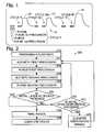
- FIG. 1is a graphical representation of the steps of the method of the invention.
- FIG. 2is a block diagram of the steps of the method of the invention.
- FIGS. 3 to 7depict successive configurations of a device constructed according to the method of the invention.
- FIG. 8depicts ALD cycles v. film thickness using the method of the invention.
- FIG. 9depicts XRR spectra for a thin film formed according to the method of the invention.
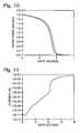
- FIGS. 10 and 11depict capacitance and current v. gate voltage for a thin film constructed according to the method of the invention, respectively.
- FIG. 12depicts a capacitance v. voltage for a thin film constructed according to the method of the invention.
- FIG. 13depicts leakage v. CET for a thin film constructed according to the method of the invention.
- the method of the inventionprovides a modified method of the invention of the above-identified related methods of the inventions, using a “no-H 2 O” technique.
- An annealis performed after every N deposition cycles, where N is an integer greater than or equal to one. This method results in films of increased density and improved dielectric quality.
- ALDis typically performed using a single precursor such as a metal halide, a metal amide, a metal organic, or an anhydrous metal nitrate. As described above, these precursors all have disadvantages.
- Hf(NO 3 ) 4 and HfCl 4were alternated to achieve high deposition rate ALD of a HfO 2 directly on H-terminated silicon. It wags demonstrated that Hf(NO 3 ) 4 could be used as an oxidizing agent for HfCl 4 , eliminating the need for H 2 O and other oxidizing agents. Although the films received a post deposition densification anneal, it was found that the density was still only ⁇ 8.5 g/cm 3 , much lower than the reported bulk value.
- Hf(NO 3 ) 4When Hf(NO 3 ) 4 is used as a precursor to deposit films via CVD, higher temperatures are used and higher densities are achieved.
- the increased densitymay be linked with improved dielectric properties because, for a given material, a higher density results in a higher refractive index and a higher dielectric constant.
- a post deposition annealresults in film densification, even when performed at high temperatures, bulk density is still not achieved.
- the “modulated temperature” method of the invention described hereinincludes ALD of dense HfO 2 films of improved dielectric quality.
- ALD filmsreceived an in-situ or ex-situ post deposition densification anneal after film deposition, i.e., after all of the ALD cycles are completed.
- the filmis annealed in-situ, after one or more ALD deposition cycles.
- the advantage of performing the anneal step after N cyclesis to efficiently remove excess ligands before the ligand buildup is so great that they cannot all be removed by the post deposition anneal.
- the inventionincludes a method of gate oxide deposition using atomic layer deposition (ALD).
- the modulated temperature profile of the method of the inventionis depicted in FIG. 1, generally at 10 , where temperature is the y-axis and time is the x-axis.
- the method of the inventionincludes, in the preferred embodiment, a pulse of an oxygen-containing first precursor, e.g., Hf(NO 3 ) 4 ; followed by a purge, e.g. with nitrogen gas, a pulse of a second precursor, e.g., HfCl 4 ; followed by another purge, e.g., nitrogen, which comprises an ALD cycle.
- the ALD cyclesare repeated until the metal oxide layer nears a critical thickness, at N cycles, at which point, an elevated temperature anneal 12 is performed.
- FIG. 1depicts the method of the invention wherein alternating ALD deposition cycles and annealing cycles are performed to fabricate a HfO 2 thin film.
- a second ALD cycle, cycle Nincludes the same precursor pulses and purges as does cycle 1 .
- ALD cycles 1 a to Naare performed until a second critical thickness is reached.
- ALD cycles and periodic elevated temperature annealsare repeated until ALD cycle Nf, when an oxide layer having a desired thickness is acquired, and a final anneal 14 at a higher temperature is performed.
- the second precursormay be a non-oxygen-containing precursor, such as HfCl 4 , or, the second precursor may be an oxygen containing precursor, and may be simply H 2 O.
- the structure prior to depositing the gate oxideis formed by any state of the art method, referred to herein as preparing the substrate.
- the example shown in the figuresis for a replacement gate process.
- the last step prior to forming the gate oxideis to expose the silicon surface to HF to prepare a H-terminated silicon surface.
- FIG. 2is a flowchart depicting the steps of the method of the invention of depositing an oxide nanolaminate thin film using a nitrate-containing first precursor as an oxidizing agent for the second precursor and annealing the substrate and the thin film after every N ALD cycles.
- a HfO 2 metal oxide layeris used as an example, however, the method of the invention will work with other metal oxides, as described later herein.
- Preparing the substrate, step 210means that the semiconductor substrate has undergone all circuit fabrication processes up to the need for a high-k dielectric film. In the case of a high-k capacitor dielectric, the substrate is prepared to have the bottom electrode ready.
- the substrateis ready to receive the gate dielectric.
- the preparationmay include the formation of device isolation structure and a gate patterning step if a metal gate process is used.
- the semiconductor substrateis prepared to have a hydrogen-terminated silicon surface.
- a hydrogen-terminated silicon surfaceis a result of many standard industry semiconductor cleaning processes. These standard cleaning processes are typically a quick immersion of the silicon wafers into an HF solution to remove any native oxide of the silicon surface and to produce a silicon surface that is hydrogen terminated.
- the hydrogen-terminated silicon surfaceis essential to remove all trace amount of native silicon oxide that could lower the effective k value of the high-k dielectric.
- Step 210provides a substrate within a process chamber.
- the substratehas undergone appropriate preparation, as described above, prior to starting the deposition, including a HF bath to provide a H-terminated silicon surface.
- the depositionnormally occurs at low pressure, typically at 1 Torr pressure, so the chamber needs to be pumped down to the base pressure, in about the milliTorr range, to reduce possible contamination.
- the substrate temperatureneeds to be prepared for the adsorption of the first precursor. Typical temperature for optimum adsorption is between 150 to 190° C., with 170° C. being a preferred temperature, however, to prevent deposition on the chamber wall, the chamber wall setting is much lower than the substrate temperature.
- the chamber wallalso needs to be at about the same temperature as the precursor vapor, typically between 50° C. and 100° C.
- An appropriate temperature for the hafnium nitrate precursoris about 88° C.
- the chamber volumeis desirably small to accelerate the saturation of precursor in the chamber volume, and the quick purging of the precursor.
- the deposition techniqueuses the chemical vapor of the precursors delivered sequentially into the process chamber, therefore the precursors need to be maintained at appropriate temperature to provide an adequate vapor pressure in the process chamber.
- gaseous precursorsi.e., precursors that are in the gaseous state at room temperature
- room temperatureis adequate.
- liquid precursorsi.e., precursors which are liquid at room temperature
- the precursor temperature settingdepends on the equilibrium vapor pressure of the liquid precursors. High volatile liquid precursors, such as alcohol and acetone, have a high equilibrium vapor pressure, so a low temperature setting at about room temperature is adequate to maintain a good vapor pressure.
- low volatile liquid precursors or solid precursorsa high temperature setting is needed. The higher the precursor temperature, the higher the precursor vapor pressure, which provides for an easier precursor delivery, so long as the temperature is set lower than a maximum precursor temperature, whereat the precursors may be damaged, such as by thermal decomposition.
- the next step, 212is the introduction of the oxygen-containing first precursor, in the preferred embodiment, a first metal nitrate-containing precursor, such as Hf(NO 3 ) 4 .
- This precursorcontains a number of nitrate ligands (NO 3 ) bonding with the first metal (Hf) which provide a source of oxygen.
- the number of nitrate ligandscan vary from 1 nitrate ligand to the maximum number of ligands to fill the valency of the metal.
- the valency of hafniumis 4 .
- the hafnium nitrate-containing precursorcan contain from 1 to 4 nitrate ligands.
- the basic concept of the method of the inventionis the use of nitrate ligands which act as oxidizers, therefore only one nitrate ligand is essential.
- the actual number of nitrate ligands in the precursormay be used as a control factor to optimize the amount of oxygen incorporated in the nanolaminate thin film.
- the precursoris purged from the process chamber, step 214 .
- the adsorption characteristicis self-limiting, therefore the precursor cannot adsorb more than one monolayer on the substrate surface, with typically only a sub-monolayer being adsorbed.
- the travel distance of the precursoris short and fairly uniform for all areas of the substrate, so the process of complete adsorption time of the precursor onto the substrate is short.
- the precursor depletion effectcan lengthen the adsorption time.
- a small chamber volumecan offer shorter adsorption time because of faster chamber saturation.
- the substrate topologycan also affect the adsorption time. In structures having deep trenches, precursor depletion effect and precursor delivery effect can lengthen the adsorption time.
- the purgingmay be accomplished by a pumping step or a replacement step to remove the first precursor from the process chamber.
- the pumping stepincludes a reduction in chamber pressure to evacuate all gases.
- the replacement stepincludes use of non-reacting gas, such as nitrogen or an inert gas, to push the remaining first precursor out of the process chamber.
- a characteristic of the replacement stepis that the chamber pressure is maintained during the purge, with the precursor turned off and the purge gas turned on.
- a combination of these two stepsmay be used in the purging step, e.g., a pumping step followed by a gas replacement step.
- a longer purge timeprovides for more complete removal of the precursor, resulting, however, in a drop in throughput. Economic reasons dictate that the shortest purging time be used, therefore the optimum purging time is such that the presence of precursor residue does not affect the overall process. Complete removal of the precursor is not required.
- the second precursorsuch as HfCl 4
- the second precursoris introduced into the process chamber in step 216 .
- the adsorbed materialseither the first metal oxide or the nitrate ligands from the first precursor or both, will react with the second metal in the second precursor to form both first metal oxide and second metal oxide in a two-oxide nanolaminate thin film structure.
- oxide nanolaminate thin filmrequires an oxidizer, such as water, oxygen, alcohol, or ozone, to form the metal oxides, and therefore requires eight separate pulses of precursor/purge/oxidizer/purge/precursor/purge/oxidizer/purge, instead of only four pulses as in the oxidizer-capable precursor/purge/precursor/purge method of the invention.
- an oxidizersuch as water, oxygen, alcohol, or ozone
- the second precursoris purged from the process chamber in step 218 .
- the purging stepmay be a pumping step, or a replacement step, or a combination of both a pumping and a replacement steps.
- Step 220asks whether the metal layer is a the desired (final) thickness. If “No,” step 222 asks whether the metal layer is near the critical thickness, e.g., that thickness where excess ligands may be efficiently removed before their buildup is so great that they can not be all removed by the post deposition (final) anneal. If the metal layer is not near the critical thickness, steps 212 to 218 are repeated, until the critical thickness is reached, at which point an in-situ, elevated temperature anneal, step 224 , is performed. The elevated temperature anneal takes place at a temperature of between about 300° C. to 850° C. for between about one second to five minutes.
- This stepis to drive off any residual ligands left over from the precursor and to density the film.
- the advantage of performing this step after N ALD cyclesis to remove the excess ligands from the just-deposited layer before the ligand buildup is too great for removal to occur in a single, post deposition annealing step.
- Steps 212 , 214 , 216 , 218 , and periodic elevated temperature anneal step 224may be repeated until a desired metal oxide layer thickness is reached, “yes” to step 220 .
- the resulting nanolaminate thin filmcan then be annealed, the final anneal, at higher temperature, such as between 400° C. to 1000° C., for between about one second to ten minutes, to improve the film quality, step 226 .
- step 228following state-of-the-art processes.
- the structure prior to depositing the gate oxideis formed by any state of the art method.
- the example shown in FIGS. 3-7is for a replacement gate process.
- a substrate 30has filled oxide regions 32 formed thereon.
- the last step prior to forming the gate oxideis to expose the silicon surface to HF to prepare a H-terminated silicon surface 34 .
- FIG. 4depicts the results of the first ALD cycle, using a pulse of Hf(NO 3 ) 4 precursor, step 212 .
- the purpose of this pulseis to initiate deposition of an HfO 2 layer 36 directly on H-terminated silicon surface 34 , without the need for an “incubation” period or a thin SiO 2 layer.
- the Hf(NO 3 ) 4 pulseis followed by a nitrogen purge, step 214 , and then pulse of HfCl 4 precursor, step 216 .
- the purpose of the HfCl 4 pulseis to complete a monolayer deposition or ALD cycle of HfO 2 layer 38 , as shown in FIG. 5. This is followed by the second purge step 218 .
- step 224is performed.
- the purpose of this stepis to drive off any residual ligands left over from the precursor and to densify the film, forming a unified, densified dielectric layer 40 , which is comprised of multiple layers 36 and 38 .
- the advantage of performing this step after every N ALD cyclesis to remove the excess ligands from the just deposited layer before the buildup is too great for removal to occur during a post deposition anneal process.
- the sequenceis repeated until the film reaches the desired, final thickness, by depositing additional unified and densified dielectric layers, such as 42 , 44 , as shown in FIG. 7, and periodic elevated temperature anneals.
- the fabrication processthen proceeds with deposition of the gate material, such as a metal gate followed by CMP.
- the remaining stepsare conventional fabrication processes.
- the process describedeliminates the need for an initial low-k interfacial layer while still achieving a film with a high dielectric constant.
- the factors which determine the critical thicknessinclude, but are not limited to, the metal oxide being deposited, chamber, substrate and precursor temperature, chamber pressure, deposition time and annealing temperature and time. It will be appreciated by those of ordinary skill in the art that N ALD cycles may be a single ALD cycle, or may be many ALD cycles, depending on the deposition conditions, the metal oxide being deposited, and the nature of the first and second precursors.
- the deposition of the first and second layers of metal ligandresults in a film having a thickness of between less than a monolayer to about 2.5 nm.
- Thicknesswas measured via spectroscopic ellipsometry.
- a plot of optical thickness at the center of the wafer vs. the number of deposition cyclesis depicted in FIG. 8, and demonstrates that thickness is linearly dependent on the number of deposition cycles. Thickness variation was less than +/ ⁇ 5% over a 6′′ wafer. The fact that the linear fit in the plot below does not intersect the x-axis confirms ease of deposition on H-terminated silicon. From the slope of the curve, a deposition rate of 0.31 nm/cycle is extracted. This deposition rate range is approximately two to four times higher than that previously reported for either Hf(NO 3 ) 4 /H 2 O or HfCl 4 /H 2 O depositions.
- Filmswere deposited via 45 cycles, with and without temperature modulation.
- the modulated temperature sampleswere annealed at ⁇ 420° C. after each deposition cycle, while the sample without temperature modulation was annealed in-situ at ⁇ 420° C. only after all of the deposition cycles were complete.
- the as-deposited thicknesswas ⁇ 14.7 nm for the film deposited with modulated temperature annealing while the thickness was ⁇ 31.8 nm for the film deposited without.
- Further post-deposition annealing at temperatures up to 650° C. for 10 min of the film deposited with out temperature modulationresulted in a thickness of 30.4 nm, a decrease of ⁇ 5%.
- the films that did not receive per cycle annealswere found to be ⁇ 8.2 g/cm 3 , indicating an increase in density of ⁇ 20% in the modulated temperature samples.
- the increased densityshould translate to improved electrical characteristics as long as crystallization is avoided.
- FIG. 13is a plot of leakage current vs. CET for modulated temperature films (squares), dual precursor film (circles), and, as a baseline, Hf(NO 3 ) 4 /H 2 O films (diamonds). It is seen that leakage of the modulated temperature films is as good as that for the baseline films. Leakage for the dual precursor films without the temperature modulation is much worse.
- FIG. 12depicts a plot of CET vs. optical thickness for modulated temperature films (squares), dual precursor film (circles), and, as a baseline, Hf(NO 3 ) 4 /H 2 O films (diamonds). It can be seen that the modulated temperatures exhibit an approximately 20% improvement in k eff . For a 5.7 nm film, with CET ⁇ 1.8, k eff ⁇ 12.5, whereas for a nitrate-only film, the effective dielectric constant is closer to 10.5.
- the “modulated temperature” ALD processshould be applicable to any ALD precursor combination for any other metal oxide, such as ZrO 2 , Gd 2 O 3 , La 2 O 3 , CeO 2 , TiO 2 , Y 2 O 3 , Ta 2 O 5 , Al 2 O 3 , HfAlO x , ZrAlO x , LaO x , etc., or a combination thereof, wherein alternating layers of oxide are deposited from nitride-containing and a chloride-containing precursors.
- any other metal oxidesuch as ZrO 2 , Gd 2 O 3 , La 2 O 3 , CeO 2 , TiO 2 , Y 2 O 3 , Ta 2 O 5 , Al 2 O 3 , HfAlO x , ZrAlO x , LaO x , etc., or a combination thereof, wherein alternating layers of oxide are deposited from nitride-containing and a chloride-containing precursors.
Landscapes
- Chemical & Material Sciences (AREA)
- Engineering & Computer Science (AREA)
- Manufacturing & Machinery (AREA)
- Chemical Kinetics & Catalysis (AREA)
- Physics & Mathematics (AREA)
- Computer Hardware Design (AREA)
- Microelectronics & Electronic Packaging (AREA)
- Power Engineering (AREA)
- Condensed Matter Physics & Semiconductors (AREA)
- General Physics & Mathematics (AREA)
- General Chemical & Material Sciences (AREA)
- Materials Engineering (AREA)
- Mechanical Engineering (AREA)
- Metallurgy (AREA)
- Organic Chemistry (AREA)
- Formation Of Insulating Films (AREA)
Abstract
Description
- This application is related to application Ser. No. 09/894,941, filed Jun. 28, 2001, for Method to initiate the atomic layer deposition of a high dielectric constant material on a silicon substrate; application Ser. No. 10/286,100, filed Oct. 31, 2002, for Method to deposit a stacked high k gate dielectric for CMOS applications, application Ser. No. 10/376,774, filed Feb. 27, 2003, for Two precursor method to perform atomic layer deposition (ALD) of a stacked high-k gate dielectric for CMOS applications, and application Ser. No. 10/376,794, filed Feb. 27, 2003, for Atomic layer deposition of nanolaminate film.[0001]
- This invention relates to a method for deposition of uniform ceramic films for a wide range of applications, such as optical coatings, passivation coatings for metallurgical and biomedical applications, and for integrated circuit fabrication, and specifically for forming a MOS gate dielectric separating a transistor gate from a channel between a source and a drain using a dual-precursor deposition and annealing process.[0002]
- Dielectric materials in semiconductor devices in integrated circuits appear as gate dielectrics in dynamic random access memory (DRAM), field effect transistors (FET) and capacitor dielectrics. The dimensions of these dielectrics are related directly to the performance of the semiconductor devices. To achieve faster responses and more complex functionality, integrated circuits are made more compact, e.g., smaller in lateral size and thickness.[0003]
- The performance of a dynamic random access memory (DRAM) device is related to the charge stored in its capacitor, which change is directly proportional to the area and dielectric constant k of the capacitor, and inversely proportional to the thickness of the capacitor. As the capacitor size decrease, a high-k dielectric is needed in the capacitor to maintain an adequate capacitance charge in a high performance DRAM device.[0004]
- The operating speed of a semiconductor device is directly proportional to the response of a gate dielectric in a field effect transistor (FET) after a voltage is applied. The response of a gate dielectric is directly proportional to the dielectric constant k and inversely proportional to the dielectric material thickness. Thus, the need for a thin and high-k dielectric is also highly desirable for a gate dielectric.[0005]
- Silicon dioxide (SiO[0006]2) is the conventional material used for gate dielectrics, having a dielectric constant of about 4. As device dimensions are scaled down, the thickness of the silicon dioxide gate dielectric reaches its tunneling limit of between about 1.5 nm to 2 nm. Silicon dioxide films of less than 1.5 nm have a high leakage from direct tunneling currents and generally cannot be used as a gate dielectric in FET devices because of excessive power consumption. Other fabrication and reliability concerns of very thin silicon dioxide films include boron penetration and charge injection damage.
- For MOS technology, thermally grown SiO[0007]2on silicon provides the dominant gate structure. The Si/SiO2interface has excellent properties, including low interface and bulk trapping, thermal stability, high breakdown, etc. With each successive generation of microelectronics technology, however, the thickness of the SiO2is scaled down. As the gate oxide thickness is scaled below 1.5 nm, problems arise, such as excessive power consumption due to current leakage from direct tunneling, boron dopant penetration, reliability concerns, etc. Because of these problems, SiO2will likely be replaced by a higher dielectric constant (k) material. A higher k material which will allow the use of a greater thickness to achieve the same capacitance. Requirements for this high-k material include lower leakage, low interface traps, low trapped charge, good reliability, good thermal stability, conformal deposition, etc.
- So far, a suitable replacement for SiO[0008]2has not been found. The most promising candidate materials are metal oxides, such as HfO2and HfxAlYOz. Because of the requirements for conformality and thickness control, atomic layer deposition (ALD) has emerged as one of the most promising deposition techniques. In this technique, dielectric material is built up layer-by-layer in a self-limiting fashion, i.e., the deposition phenomenon where only one monolayer of a chemical species will adsorb onto a given surface.
- In ALD, the precursor vapors are injected into the process chamber in alternating sequences: precursor, purge gas, reactant, purge gas. The precursor adsorbs onto the substrate and subsequently reacts with the reactant. There are various modifications of the ALD processes, however, basic ALD processes all contain two distinct properties: alternating injection of precursors and the saturation of the precursor adsorption. By alternating precursors and reactants in the vapor stream, separated by a purge gas, the possibility of gas phase reaction is minimized, allowing a wide range of possible precursors. Also, because of the self-limiting nature of the chemisorption mechanism, the deposited film is extremely uniform, because once the surface is saturated, the additional precursors and reactants will not further adsorb or react and will be exhausted away.[0009]
- The precursor requirements of ALD are different from those of CVD because of the different deposition mechanisms. ALD precursors must exhibit a temperature range between condensation and decomposition and have a self-limiting effect, so that only a monolayer of precursor is adsorbed on the substrate. Precursors designed for ALD use must readily adsorb at bonding sites on the deposited surface in a self-limiting mode. Once adsorbed, the precursors must react with the reactants to form the desired film. In CVI), the precursors and the reactants arrive at the substrate together and the film is deposited continuously from the reaction of the precursors with the reactants. The deposition rate in CVD process is proportional to the precursor and reactant flow rate and to the substrate temperature. In CVD, the precursor and the reactant must react at the deposited surface simultaneously to form the desired film. Thus many useful CVD precursors are not viable as ALD precursors and vice versa. It is not trivial or obvious to select a precursor for the ALD method.[0010]
- Currently, the leading ALD precursors for depositing metal oxides are metal organics, metal halides, metal amides, and anhydrous metal nitrates. These precursors all have serious drawbacks. Metal organics have the potential to introduce organic contamination into the IC structure during the fabrication process, leading to degraded IC performance.[0011]
- HfO[0012]2and ZrO2films deposited using a metal halide precursor, such as [M+]Cl4, demonstrate good insulating properties, including high dielectric constant and low leakage, however, they do not provide smooth deposition directly on H-terminated silicon and require several “incubation” cycles, which may result in roughening. For uniform initiation, they require several monolayers of SiO2or Si3N4. Because even a very thin low-k layer can negate most of the benefits of an overlying high-k layer, the presence of several monolayers of SiO2makes it difficult to achieve EOT<1.0 nm using this type of precursor. Deposition directly on hydrogen-terminated silicon is essential. This initiation problem must be solved before metal-chloride precursors can be used in production.
- The nitrate (NO[0013]3) ligand is a powerful oxidizing and nitriding agent, and capable of reacting strongly with many compounds. Gates et al., U.S. Pat. No. 6,203,613, granted Mar. 20, 2001, for Atomic layer deposition with nitrate containing precursors, describes an ALD method using metal nitrate precursors in conjunction with oxidizing, nitriding and reducing co-reactants to deposit oxide, nitride and metal films, respectively.
- Ono et al., in U.S. Pat. No. 6,420,279, granted Jul. 16, 2002, for Method of using atomic layer deposition to deposit a high dielectric constant material on a substrate, for example, describes ALD deposition of zirconium oxide using zirconium nitrate precursor, together with an oxidizing agent, such as water or methanol; and the ALD deposition of hafnium oxide using a hafnium nitrate precursor together with an oxidizing agent, such as water or methanol, which patent is incorporated herein by reference.[0014]
- A metal nitrate precursor, Hf(NO[0015]3)4has recently been demonstrated as a viable ALD precursor, in the first-above-identified related Application and in Conley et al., Atomic layer deposition of hafnium oxide using anhydrous hafnium nitrate, Electrochemical and Solid-State Letters, 5 (5), C57-59 (2002). The primary benefit of Hf(NO3)4is that it allows deposition initiation directly on H-terminated silicon, resulting in a uniform thin layer, without the requirement of an initial layer of low-k material. However, as previously noted, HfO2films deposited via ALD of Hf(NO3)4have a dielectric constant that is lower than expected, possibly due to the low density of the films (˜8.5 g/cm3vs. a bulk value of 9.7 g/cm3), even after a post deposition anneal of up to 850° C. The low film density may be a result of the low deposition temperature (170° C.) required for use of this precursor. Before metal-nitrate precursors can find widespread use, the “bulk” dielectric properties of the resulting films must be improved.
- In addition, films produced by all of the above-described methods suffer from poor channel mobility when integrated into an MOS device structure.[0016]
- Yet another problem with traditional method of ALD is the presence of silicon oxide at the wafer interface. This layer forms because, in addition to the requirement for a metal precursor, an oxidizing precursor is also required, which promotes formation of silicon oxide. The oxidizing precursor produces an unwanted SiO[0017]2layer between the wafer surface and the metal oxide film.
- The use of water vapor introduces a number of problems: The introduction of the necessary quantity of water vapor is difficult to control, and typically, an abundance of water vapor is introduced into the chamber. Water is a polar molecule, and adsorbs efficiently onto surfaces, i.e., the chamber walls. Desorption of water vapor, e.g., via vacuum pumping, adds considerable time to the overall process time, reducing the throughput.[0018]
- The second through fourth above-identified related patents and patent applications describe methods to improve the quality of the ALD metal-oxide films in which a combination of precursors is used. The use of a combination of precursors provides the advantages of each precursor while minimizing the disadvantages. The “dual-precursor” methods described in the related applications allows for more efficient ALD of HfO[0019]2, while negating the need for a separate oxidizing source, such as H2O. However, although the films received a post deposition densification anneal, it was found that the density was still only ˜8.5 g/cm3, much lower than the reported bulk value.
- A method of forming a layer of high-k dielectric material in an integrated circuit includes preparing a silicon substrate; forming a high-k dielectric layer by a sequence of ALD cycles including: depositing a first layer of metal ligand using ALD with an oxygen-containing first precursor; and depositing a second layer of metal ligand using ALD with a second precursor; repeating the sequence of ALD cycles N times until a near-critical thickness of metal oxide is formed; annealing the substrate and metal oxide layers every N ALD cycles in an elevated temperature anneal; repeating the sequence of ALD cycles and elevated temperature anneals until a high-k dielectric layer of desired thickness is formed; annealing the substrate and the metal oxide layers in a final annealing step; and completing the integrated circuit.[0020]
- It is an object of the invention to provide a very uniform deposition of dense metal oxide films at low temperatures.[0021]
- Another object of the invention is to provide a method of efficiently removing excess ligands before the ligand buildup is so great that the ligands cannot all be removed by a post deposition anneal.[0022]
- Another object of the invention to provide a very uniform deposition of dense metal oxide films without use of an oxidizing species, such as oxygen or water.[0023]
- It is a further object of the invention to provide a very uniform deposition of dense hafnia films at low temperature without use of an oxidizing species such as oxygen or water.[0024]
- Another object of the invention is to provide a hafnia on a H-terminated silicon surface.[0025]
- This summary and objectives of the invention are provided to enable quick comprehension of the nature of the invention. A more thorough understanding of the invention may be obtained by reference to the following detailed description of the preferred embodiment of the invention in connection with the drawings.[0026]
- FIG. 1 is a graphical representation of the steps of the method of the invention.[0027]
- FIG. 2 is a block diagram of the steps of the method of the invention.[0028]
- FIGS.[0029]3 to7 depict successive configurations of a device constructed according to the method of the invention.
- FIG. 8 depicts ALD cycles v. film thickness using the method of the invention.[0030]
- FIG. 9 depicts XRR spectra for a thin film formed according to the method of the invention.[0031]
- FIGS. 10 and 11 depict capacitance and current v. gate voltage for a thin film constructed according to the method of the invention, respectively.[0032]
- FIG. 12 depicts a capacitance v. voltage for a thin film constructed according to the method of the invention.[0033]
- FIG. 13 depicts leakage v. CET for a thin film constructed according to the method of the invention.[0034]
- The method of the invention provides a modified method of the invention of the above-identified related methods of the inventions, using a “no-H[0035]2O” technique. An anneal is performed after every N deposition cycles, where N is an integer greater than or equal to one. This method results in films of increased density and improved dielectric quality.
- The present state of the art for gate formation involves oxidation of silicon at high temperatures. It is likely, however, that in the near future, SiO[0036]2will be replaced by a metal-oxide such as HfO2, ZrO2, etc. Although a high-k deposition method has not been established yet, a leading technique is atomic layer chemical vapor deposition (ALD or ALCVD).
- ALD is typically performed using a single precursor such as a metal halide, a metal amide, a metal organic, or an anhydrous metal nitrate. As described above, these precursors all have disadvantages.[0037]
- In a related application, two precursors, Hf(NO[0038]3)4and HfCl4, were alternated to achieve high deposition rate ALD of a HfO2directly on H-terminated silicon. It wags demonstrated that Hf(NO3)4could be used as an oxidizing agent for HfCl4, eliminating the need for H2O and other oxidizing agents. Although the films received a post deposition densification anneal, it was found that the density was still only ˜8.5 g/cm3, much lower than the reported bulk value.
- When Hf(NO[0039]3)4is used as a precursor to deposit films via CVD, higher temperatures are used and higher densities are achieved. The increased density may be linked with improved dielectric properties because, for a given material, a higher density results in a higher refractive index and a higher dielectric constant. Although a post deposition anneal results in film densification, even when performed at high temperatures, bulk density is still not achieved.
- The “modulated temperature” method of the invention described herein includes ALD of dense HfO[0040]2films of improved dielectric quality. Previously, ALD films received an in-situ or ex-situ post deposition densification anneal after film deposition, i.e., after all of the ALD cycles are completed. In the present invention, the film is annealed in-situ, after one or more ALD deposition cycles. The advantage of performing the anneal step after N cycles is to efficiently remove excess ligands before the ligand buildup is so great that they cannot all be removed by the post deposition anneal. The invention includes a method of gate oxide deposition using atomic layer deposition (ALD).
- The use of “modulated temperature” ALD, in which in-situ anneals are performed after each N deposition cycle, is demonstrated to provide a better thin film than in the above-identified related applications. Each anneal allows easier ligand removal from the just-deposited layer and results in densification and a concomitant increase in dielectric constant of the resulting films. In the related cases, films were deposited using the “dual-precursor” technique, e.g., Hf(NO[0041]3)4and HfCl4precursors were used. Hf(NO3)4allows deposition directly on H-terminated silicon and serves as an oxidizing agent for HfCl4. H2O does not need to be used. The modulated temperature profile of the method of the invention is depicted in FIG. 1, generally at10, where temperature is the y-axis and time is the x-axis. The method of the invention includes, in the preferred embodiment, a pulse of an oxygen-containing first precursor, e.g., Hf(NO3)4; followed by a purge, e.g. with nitrogen gas, a pulse of a second precursor, e.g., HfCl4; followed by another purge, e.g., nitrogen, which comprises an ALD cycle. The ALD cycles are repeated until the metal oxide layer nears a critical thickness, at N cycles, at which point, an
elevated temperature anneal 12 is performed. The ALD cycle and periodic elevated temperature anneal are repeated to produce a film of desired thickness. In order to immediately initiate deposition directly on hydrogen terminated silicon, the Hf(NO3)4pulse must start the sequence. FIG. 1 depicts the method of the invention wherein alternating ALD deposition cycles and annealing cycles are performed to fabricate a HfO2thin film. A second ALD cycle, cycle N, includes the same precursor pulses and purges as doescycle 1. ALD cycles1ato Na are performed until a second critical thickness is reached. ALD cycles and periodic elevated temperature anneals are repeated until ALD cycle Nf, when an oxide layer having a desired thickness is acquired, and afinal anneal 14 at a higher temperature is performed. The second precursor may be a non-oxygen-containing precursor, such as HfCl4, or, the second precursor may be an oxygen containing precursor, and may be simply H2O. - The structure prior to depositing the gate oxide is formed by any state of the art method, referred to herein as preparing the substrate. The example shown in the figures is for a replacement gate process. The last step prior to forming the gate oxide is to expose the silicon surface to HF to prepare a H-terminated silicon surface.[0042]
- FIG. 2 is a flowchart depicting the steps of the method of the invention of depositing an oxide nanolaminate thin film using a nitrate-containing first precursor as an oxidizing agent for the second precursor and annealing the substrate and the thin film after every N ALD cycles. The formation of a HfO[0043]2metal oxide layer is used as an example, however, the method of the invention will work with other metal oxides, as described later herein. Preparing the substrate,
step 210, means that the semiconductor substrate has undergone all circuit fabrication processes up to the need for a high-k dielectric film. In the case of a high-k capacitor dielectric, the substrate is prepared to have the bottom electrode ready. In the case of a high-k gate dielectric, the substrate is ready to receive the gate dielectric. The preparation may include the formation of device isolation structure and a gate patterning step if a metal gate process is used. Then the semiconductor substrate is prepared to have a hydrogen-terminated silicon surface. A hydrogen-terminated silicon surface is a result of many standard industry semiconductor cleaning processes. These standard cleaning processes are typically a quick immersion of the silicon wafers into an HF solution to remove any native oxide of the silicon surface and to produce a silicon surface that is hydrogen terminated. The hydrogen-terminated silicon surface is essential to remove all trace amount of native silicon oxide that could lower the effective k value of the high-k dielectric. Experiments have shown that a combination of hafnium nitrate precursor and a hydrogen-terminated silicon surface can result in the initiation of the deposition of hafnium oxide directly on the hydrogen-terminated silicon surface without the need for an incubation period or the need for a thin silicon dioxide interfacial layer. Conley et al., supra. - [0044]
Step 210 provides a substrate within a process chamber. The substrate has undergone appropriate preparation, as described above, prior to starting the deposition, including a HF bath to provide a H-terminated silicon surface. The deposition normally occurs at low pressure, typically at 1 Torr pressure, so the chamber needs to be pumped down to the base pressure, in about the milliTorr range, to reduce possible contamination. The substrate temperature needs to be prepared for the adsorption of the first precursor. Typical temperature for optimum adsorption is between 150 to 190° C., with 170° C. being a preferred temperature, however, to prevent deposition on the chamber wall, the chamber wall setting is much lower than the substrate temperature. To prevent condensation of the precursor, the chamber wall also needs to be at about the same temperature as the precursor vapor, typically between 50° C. and 100° C. An appropriate temperature for the hafnium nitrate precursor is about 88° C. There are no other special settings for the chamber. Because this process uses atomic layer deposition technique, meaning a sequence of precursor pulses, the chamber volume is desirably small to accelerate the saturation of precursor in the chamber volume, and the quick purging of the precursor. - The deposition technique uses the chemical vapor of the precursors delivered sequentially into the process chamber, therefore the precursors need to be maintained at appropriate temperature to provide an adequate vapor pressure in the process chamber. For gaseous precursors, i.e., precursors that are in the gaseous state at room temperature, room temperature is adequate. For liquid precursors, i.e., precursors which are liquid at room temperature, the precursor temperature setting depends on the equilibrium vapor pressure of the liquid precursors. High volatile liquid precursors, such as alcohol and acetone, have a high equilibrium vapor pressure, so a low temperature setting at about room temperature is adequate to maintain a good vapor pressure. For low volatile liquid precursors or solid precursors, a high temperature setting is needed. The higher the precursor temperature, the higher the precursor vapor pressure, which provides for an easier precursor delivery, so long as the temperature is set lower than a maximum precursor temperature, whereat the precursors may be damaged, such as by thermal decomposition.[0045]
- After the preparation of the process chamber and the substrate, the next step,[0046]212, is the introduction of the oxygen-containing first precursor, in the preferred embodiment, a first metal nitrate-containing precursor, such as Hf(NO3)4. This precursor contains a number of nitrate ligands (NO3) bonding with the first metal (Hf) which provide a source of oxygen. Depending on the valency of the first metal, the number of nitrate ligands can vary from 1 nitrate ligand to the maximum number of ligands to fill the valency of the metal. For example, the valency of hafnium is4. Therefore, the hafnium nitrate-containing precursor can contain from 1 to 4 nitrate ligands. The basic concept of the method of the invention is the use of nitrate ligands which act as oxidizers, therefore only one nitrate ligand is essential. The actual number of nitrate ligands in the precursor may be used as a control factor to optimize the amount of oxygen incorporated in the nanolaminate thin film.
- After an appropriate time, which generally requires between about 0.1 seconds to 100 seconds, to allow the complete adsorption of the first metal nitrate-containing precursor onto the substrate, the precursor is purged from the process chamber,[0047]
step 214. The adsorption characteristic is self-limiting, therefore the precursor cannot adsorb more than one monolayer on the substrate surface, with typically only a sub-monolayer being adsorbed. In a chamber using a showerhead delivery, the travel distance of the precursor is short and fairly uniform for all areas of the substrate, so the process of complete adsorption time of the precursor onto the substrate is short. In contrast, if the precursor is designed to deliver from one end and exhaust from the other end of the process chamber, the precursor depletion effect can lengthen the adsorption time. Similarly, a small chamber volume can offer shorter adsorption time because of faster chamber saturation. The substrate topology can also affect the adsorption time. In structures having deep trenches, precursor depletion effect and precursor delivery effect can lengthen the adsorption time. - The purging may be accomplished by a pumping step or a replacement step to remove the first precursor from the process chamber. The pumping step includes a reduction in chamber pressure to evacuate all gases. The replacement step includes use of non-reacting gas, such as nitrogen or an inert gas, to push the remaining first precursor out of the process chamber. A characteristic of the replacement step is that the chamber pressure is maintained during the purge, with the precursor turned off and the purge gas turned on. A combination of these two steps may be used in the purging step, e.g., a pumping step followed by a gas replacement step.[0048]
- A longer purge time provides for more complete removal of the precursor, resulting, however, in a drop in throughput. Economic reasons dictate that the shortest purging time be used, therefore the optimum purging time is such that the presence of precursor residue does not affect the overall process. Complete removal of the precursor is not required.[0049]
- After the chamber is free from the first precursor, the second precursor, such as HfCl[0050]4, is introduced into the process chamber in
step 216. The adsorbed materials, either the first metal oxide or the nitrate ligands from the first precursor or both, will react with the second metal in the second precursor to form both first metal oxide and second metal oxide in a two-oxide nanolaminate thin film structure. The known prior art process of oxide nanolaminate thin film requires an oxidizer, such as water, oxygen, alcohol, or ozone, to form the metal oxides, and therefore requires eight separate pulses of precursor/purge/oxidizer/purge/precursor/purge/oxidizer/purge, instead of only four pulses as in the oxidizer-capable precursor/purge/precursor/purge method of the invention. - After the nanolaminate formation, the second precursor is purged from the process chamber in[0051]
step 218. Again, the purging step may be a pumping step, or a replacement step, or a combination of both a pumping and a replacement steps. - [0052]
Step 220 asks whether the metal layer is a the desired (final) thickness. If “No,”step 222 asks whether the metal layer is near the critical thickness, e.g., that thickness where excess ligands may be efficiently removed before their buildup is so great that they can not be all removed by the post deposition (final) anneal. If the metal layer is not near the critical thickness, steps212 to218 are repeated, until the critical thickness is reached, at which point an in-situ, elevated temperature anneal,step 224, is performed. The elevated temperature anneal takes place at a temperature of between about 300° C. to 850° C. for between about one second to five minutes. The purpose of this step is to drive off any residual ligands left over from the precursor and to density the film. The advantage of performing this step after N ALD cycles is to remove the excess ligands from the just-deposited layer before the ligand buildup is too great for removal to occur in a single, post deposition annealing step. - [0053]
Steps temperature anneal step 224, may be repeated until a desired metal oxide layer thickness is reached, “yes” to step220, The resulting nanolaminate thin film can then be annealed, the final anneal, at higher temperature, such as between 400° C. to 1000° C., for between about one second to ten minutes, to improve the film quality,step 226. After the final annealing step, device completion takes place,step 228, following state-of-the-art processes. - The structure prior to depositing the gate oxide is formed by any state of the art method. The example shown in FIGS. 3-7 is for a replacement gate process. Referring to FIG. 3, a[0054]
substrate 30 has filledoxide regions 32 formed thereon. The last step prior to forming the gate oxide is to expose the silicon surface to HF to prepare a H-terminatedsilicon surface 34. - FIG. 4 depicts the results of the first ALD cycle, using a pulse of Hf(NO[0055]3)4precursor,
step 212. The purpose of this pulse is to initiate deposition of an HfO2layer36 directly on H-terminatedsilicon surface 34, without the need for an “incubation” period or a thin SiO2layer. - The Hf(NO[0056]3)4pulse is followed by a nitrogen purge,
step 214, and then pulse of HfCl4precursor,step 216. The purpose of the HfCl4pulse is to complete a monolayer deposition or ALD cycle of HfO2layer38, as shown in FIG. 5. This is followed by thesecond purge step 218. - After N ALD cycles, multiple oxide layers are present on the substrate as the critical thickness is reached. An in-situ elevated temperature anneal,[0057]
step 224, is performed. The purpose of this step is to drive off any residual ligands left over from the precursor and to densify the film, forming a unified, densifieddielectric layer 40, which is comprised ofmultiple layers - The sequence is repeated until the film reaches the desired, final thickness, by depositing additional unified and densified dielectric layers, such as[0058]42,44, as shown in FIG. 7, and periodic elevated temperature anneals. The fabrication process then proceeds with deposition of the gate material, such as a metal gate followed by CMP. The remaining steps are conventional fabrication processes. The process described eliminates the need for an initial low-k interfacial layer while still achieving a film with a high dielectric constant. The factors which determine the critical thickness include, but are not limited to, the metal oxide being deposited, chamber, substrate and precursor temperature, chamber pressure, deposition time and annealing temperature and time. It will be appreciated by those of ordinary skill in the art that N ALD cycles may be a single ALD cycle, or may be many ALD cycles, depending on the deposition conditions, the metal oxide being deposited, and the nature of the first and second precursors.
- The deposition of the first and second layers of metal ligand results in a film having a thickness of between less than a monolayer to about 2.5 nm.[0059]
- An example of demonstrated utility of the method of the invention follows: HfO[0060]2films were deposited on H-terminated silicon using 10, 15, and 45 cycles of Hf(NO3)4/HfCl4/and periodic elevated temperature anneal, as described above. The resulting films were visually uniform. In this example, the films were annealed after every ALD cycle, e.g., N=1. Control films were also deposited in which the films were annealed only after the deposition was complete.
- Thickness was measured via spectroscopic ellipsometry. A plot of optical thickness at the center of the wafer vs. the number of deposition cycles is depicted in FIG. 8, and demonstrates that thickness is linearly dependent on the number of deposition cycles. Thickness variation was less than +/−5% over a 6″ wafer. The fact that the linear fit in the plot below does not intersect the x-axis confirms ease of deposition on H-terminated silicon. From the slope of the curve, a deposition rate of 0.31 nm/cycle is extracted. This deposition rate range is approximately two to four times higher than that previously reported for either Hf(NO[0061]3)4/H2O or HfCl4/H2O depositions. Based solely on Hf application, an approximate two times increase is expected. However, this rate is lower that the 0.7 nm/cycle that is observed for the dual precursor films that were annealed only after the deposition was complete. This suggests that the extra anneals, following N ALD cycles, serve to densify the film.
- Films were deposited via 45 cycles, with and without temperature modulation. The modulated temperature samples were annealed at ˜420° C. after each deposition cycle, while the sample without temperature modulation was annealed in-situ at ˜420° C. only after all of the deposition cycles were complete. The as-deposited thickness was ˜14.7 nm for the film deposited with modulated temperature annealing while the thickness was ˜31.8 nm for the film deposited without. Further post-deposition annealing at temperatures up to 650° C. for 10 min of the film deposited with out temperature modulation resulted in a thickness of 30.4 nm, a decrease of ˜5%. Another film that was deposited using the modulated temperature anneal of the method of the invention and annealed for 20 min at 600° C. decreased in thickness by only ˜8%. These results indicate that reasonable post deposition anneals are unable to achieve the same level of densification as anneals conducted after each ALD cycle.[0062]
- Referring now to FIG. 9, SE measurements revealed that the films could be modeled as transparent, with n=2.05 at K=632.8 nm. This is a higher refractive index than the n=1.96 that was found for the HfO[0063]2films that were annealed only at the end of all of the deposition cycles. A higher refractive index indicates densification of the film. As a further indication of densification, XRR spectra are shown above at right. Modeling of the XRR data indicates that the density of the modulated temperature film is approximately 9.8 g/cm3, about equal to the bulk value of 9.7 g/cm3. The films that did not receive per cycle anneals were found to be ˜8.2 g/cm3, indicating an increase in density of ˜20% in the modulated temperature samples. The increased density should translate to improved electrical characteristics as long as crystallization is avoided.
- TiN gate capacitors were formed using a photolithographic process. TiN patterning was followed by a 30 min, 450° C. anneal in N[0064]2/H2. A sample capacitance vs. voltage curve is depicted in FIG. 10. Hysteresis is fairly low. A sample leakage current vs. gate voltage is depicted in FIG. 11. Hard breakdown occurs at approximately 4.2 V for a CET=1.9 nm film, corresponding to an effective BD field of ˜22 MV/cm.
- FIG. 13 is a plot of leakage current vs. CET for modulated temperature films (squares), dual precursor film (circles), and, as a baseline, Hf(NO[0065]3)4/H2O films (diamonds). It is seen that leakage of the modulated temperature films is as good as that for the baseline films. Leakage for the dual precursor films without the temperature modulation is much worse. FIG. 12 depicts a plot of CET vs. optical thickness for modulated temperature films (squares), dual precursor film (circles), and, as a baseline, Hf(NO3)4/H2O films (diamonds). It can be seen that the modulated temperatures exhibit an approximately 20% improvement in keff. For a 5.7 nm film, with CET˜1.8, keff˜12.5, whereas for a nitrate-only film, the effective dielectric constant is closer to 10.5.
- The “modulated temperature” ALD process should be applicable to any ALD precursor combination for any other metal oxide, such as ZrO[0066]2, Gd2O3, La2O3, CeO2, TiO2, Y2O3, Ta2O5, Al2O3, HfAlOx, ZrAlOx, LaOx, etc., or a combination thereof, wherein alternating layers of oxide are deposited from nitride-containing and a chloride-containing precursors.
- Thus, a method for modulated temperature ALD has been disclosed. It will be appreciated that further variations and modifications thereof may be made within the scope of the invention as defined in the appended claims.[0067]
Claims (25)
Priority Applications (1)
| Application Number | Priority Date | Filing Date | Title |
|---|---|---|---|
| US10/412,550US7442415B2 (en) | 2003-04-11 | 2003-04-11 | Modulated temperature method of atomic layer deposition (ALD) of high dielectric constant films |
Applications Claiming Priority (1)
| Application Number | Priority Date | Filing Date | Title |
|---|---|---|---|
| US10/412,550US7442415B2 (en) | 2003-04-11 | 2003-04-11 | Modulated temperature method of atomic layer deposition (ALD) of high dielectric constant films |
Publications (2)
| Publication Number | Publication Date |
|---|---|
| US20040203254A1true US20040203254A1 (en) | 2004-10-14 |
| US7442415B2 US7442415B2 (en) | 2008-10-28 |
Family
ID=33131247
Family Applications (1)
| Application Number | Title | Priority Date | Filing Date |
|---|---|---|---|
| US10/412,550Expired - LifetimeUS7442415B2 (en) | 2003-04-11 | 2003-04-11 | Modulated temperature method of atomic layer deposition (ALD) of high dielectric constant films |
Country Status (1)
| Country | Link |
|---|---|
| US (1) | US7442415B2 (en) |
Cited By (114)
| Publication number | Priority date | Publication date | Assignee | Title |
|---|---|---|---|---|
| US20040168627A1 (en)* | 2003-02-27 | 2004-09-02 | Sharp Laboratories Of America, Inc. | Atomic layer deposition of oxide film |
| US20050142769A1 (en)* | 2003-12-25 | 2005-06-30 | Yoshiki Kamata | Semiconductor device and method for manufacturing the same |
| US20050153571A1 (en)* | 2003-11-17 | 2005-07-14 | Yoshihide Senzaki | Nitridation of high-k dielectric films |
| US20050271812A1 (en)* | 2004-05-12 | 2005-12-08 | Myo Nyi O | Apparatuses and methods for atomic layer deposition of hafnium-containing high-k dielectric materials |
| US20060081905A1 (en)* | 2004-10-15 | 2006-04-20 | Samsung Electronics Co., Ltd. | Dielectric multilayer of microelectronic device and method of fabricating the same |
| US20060138552A1 (en)* | 2004-09-30 | 2006-06-29 | Brask Justin K | Nonplanar transistors with metal gate electrodes |
| US7081421B2 (en) | 2004-08-26 | 2006-07-25 | Micron Technology, Inc. | Lanthanide oxide dielectric layer |
| US20060180879A1 (en)* | 2005-02-16 | 2006-08-17 | Maes Jan W | Method to enhance the initiation of film growth |
| EP1693888A1 (en)* | 2005-02-16 | 2006-08-23 | Interuniversitair Microelektronica Centrum ( Imec) | Method to enhance the initiation of film growth |
| US20060244100A1 (en)* | 2005-04-28 | 2006-11-02 | Micron Technology, Inc. | Atomic layer deposited zirconium silicon oxide films |
| US7135418B1 (en)* | 2005-03-09 | 2006-11-14 | Novellus Systems, Inc. | Optimal operation of conformal silica deposition reactors |
| US7160577B2 (en) | 2002-05-02 | 2007-01-09 | Micron Technology, Inc. | Methods for atomic-layer deposition of aluminum oxides in integrated circuits |
| US7163899B1 (en) | 2004-10-26 | 2007-01-16 | Novellus Systems, Inc. | Localized energy pulse rapid thermal anneal dielectric film densification method |
| US20070037415A1 (en)* | 2004-12-13 | 2007-02-15 | Micron Technology, Inc. | Lanthanum hafnium oxide dielectrics |
| US7183186B2 (en) | 2003-04-22 | 2007-02-27 | Micro Technology, Inc. | Atomic layer deposited ZrTiO4 films |
| US20070048989A1 (en)* | 2005-08-30 | 2007-03-01 | Micron Technology, Inc. | Atomic layer deposition of GdScO3 films as gate dielectrics |
| US7192892B2 (en)* | 2003-03-04 | 2007-03-20 | Micron Technology, Inc. | Atomic layer deposited dielectric layers |
| US7192824B2 (en) | 2003-06-24 | 2007-03-20 | Micron Technology, Inc. | Lanthanide oxide / hafnium oxide dielectric layers |
| US20070077776A1 (en)* | 2003-03-24 | 2007-04-05 | Tominaga Koji | Method for forming an insulating film in a semiconductor device |
| US7202185B1 (en) | 2004-06-22 | 2007-04-10 | Novellus Systems, Inc. | Silica thin films produced by rapid surface catalyzed vapor deposition (RVD) using a nucleation layer |
| US7208413B2 (en) | 2000-06-27 | 2007-04-24 | Applied Materials, Inc. | Formation of boride barrier layers using chemisorption techniques |
| US7223707B1 (en) | 2004-12-30 | 2007-05-29 | Novellus Systems, Inc. | Dynamic rapid vapor deposition process for conformal silica laminates |
| US7259434B2 (en) | 2001-08-30 | 2007-08-21 | Micron Technology, Inc. | Highly reliable amorphous high-k gate oxide ZrO2 |
| US7271112B1 (en) | 2004-12-30 | 2007-09-18 | Novellus Systems, Inc. | Methods for forming high density, conformal, silica nanolaminate films via pulsed deposition layer in structures of confined geometry |
| US20070218290A1 (en)* | 2004-06-24 | 2007-09-20 | Beneq Oy | Method for Doping Material and Doped Material |
| US7294583B1 (en) | 2004-12-23 | 2007-11-13 | Novellus Systems, Inc. | Methods for the use of alkoxysilanol precursors for vapor deposition of SiO2 films |
| US7297608B1 (en) | 2004-06-22 | 2007-11-20 | Novellus Systems, Inc. | Method for controlling properties of conformal silica nanolaminates formed by rapid vapor deposition |
| US20070269982A1 (en)* | 2006-05-18 | 2007-11-22 | Rocklein M Noel | Method and device to vary growth rate of thin films over semiconductor structures |
| US7304004B2 (en) | 2002-06-14 | 2007-12-04 | Applied Materials, Inc. | System and method for forming a gate dielectric |
| US20070277735A1 (en)* | 2006-06-02 | 2007-12-06 | Nima Mokhlesi | Systems for Atomic Layer Deposition of Oxides Using Krypton as an Ion Generating Feeding Gas |
| US20070281105A1 (en)* | 2006-06-02 | 2007-12-06 | Nima Mokhlesi | Atomic Layer Deposition of Oxides Using Krypton as an Ion Generating Feeding Gas |
| US20070281082A1 (en)* | 2006-06-02 | 2007-12-06 | Nima Mokhlesi | Flash Heating in Atomic Layer Deposition |
| US7342984B1 (en) | 2003-04-03 | 2008-03-11 | Zilog, Inc. | Counting clock cycles over the duration of a first character and using a remainder value to determine when to sample a bit of a second character |
| US7352048B2 (en) | 2001-09-26 | 2008-04-01 | Applied Materials, Inc. | Integration of barrier layer and seed layer |
| US20080081114A1 (en)* | 2006-10-03 | 2008-04-03 | Novellus Systems, Inc. | Apparatus and method for delivering uniform fluid flow in a chemical deposition system |
| US7402534B2 (en) | 2005-08-26 | 2008-07-22 | Applied Materials, Inc. | Pretreatment processes within a batch ALD reactor |
| US7402210B2 (en) | 2002-11-14 | 2008-07-22 | Applied Materials, Inc. | Apparatus and method for hybrid chemical processing |
| US7410668B2 (en) | 2001-03-01 | 2008-08-12 | Micron Technology, Inc. | Methods, systems, and apparatus for uniform chemical-vapor depositions |
| US7416979B2 (en) | 2001-07-25 | 2008-08-26 | Applied Materials, Inc. | Deposition methods for barrier and tungsten materials |
| US7429361B2 (en) | 2002-07-17 | 2008-09-30 | Applied Materials, Inc. | Method and apparatus for providing precursor gas to a processing chamber |
| US7456476B2 (en) | 2003-06-27 | 2008-11-25 | Intel Corporation | Nonplanar semiconductor device with partially or fully wrapped around gate electrode and methods of fabrication |
| US7479421B2 (en) | 2005-09-28 | 2009-01-20 | Intel Corporation | Process for integrating planar and non-planar CMOS transistors on a bulk substrate and article made thereby |
| US7491653B1 (en) | 2005-12-23 | 2009-02-17 | Novellus Systems, Inc. | Metal-free catalysts for pulsed deposition layer process for conformal silica laminates |
| US7494939B2 (en) | 2004-08-31 | 2009-02-24 | Micron Technology, Inc. | Methods for forming a lanthanum-metal oxide dielectric layer |
| US7498247B2 (en) | 2005-02-23 | 2009-03-03 | Micron Technology, Inc. | Atomic layer deposition of Hf3N4/HfO2 films as gate dielectrics |
| US7508648B2 (en) | 2005-02-08 | 2009-03-24 | Micron Technology, Inc. | Atomic layer deposition of Dy doped HfO2 films as gate dielectrics |
| US7514358B2 (en) | 2002-03-04 | 2009-04-07 | Applied Materials, Inc. | Sequential deposition of tantalum nitride using a tantalum-containing precursor and a nitrogen-containing precursor |
| US7518196B2 (en) | 2005-02-23 | 2009-04-14 | Intel Corporation | Field effect transistor with narrow bandgap source and drain regions and method of fabrication |
| US7547952B2 (en) | 2003-04-04 | 2009-06-16 | Applied Materials, Inc. | Method for hafnium nitride deposition |
| US7547637B2 (en) | 2005-06-21 | 2009-06-16 | Intel Corporation | Methods for patterning a semiconductor film |
| US7550333B2 (en) | 2004-10-25 | 2009-06-23 | Intel Corporation | Nonplanar device with thinned lower body portion and method of fabrication |
| US7560793B2 (en) | 2002-05-02 | 2009-07-14 | Micron Technology, Inc. | Atomic layer deposition and conversion |
| US7560395B2 (en) | 2005-01-05 | 2009-07-14 | Micron Technology, Inc. | Atomic layer deposited hafnium tantalum oxide dielectrics |
| EP1693889A3 (en)* | 2005-02-16 | 2009-08-12 | Imec | Method to enhance the initiation of film growth |
| US7579280B2 (en) | 2004-06-01 | 2009-08-25 | Intel Corporation | Method of patterning a film |
| US7588988B2 (en) | 2004-08-31 | 2009-09-15 | Micron Technology, Inc. | Method of forming apparatus having oxide films formed using atomic layer deposition |
| US7589028B1 (en) | 2005-11-15 | 2009-09-15 | Novellus Systems, Inc. | Hydroxyl bond removal and film densification method for oxide films using microwave post treatment |
| US7601648B2 (en) | 2006-07-31 | 2009-10-13 | Applied Materials, Inc. | Method for fabricating an integrated gate dielectric layer for field effect transistors |
| US7605030B2 (en) | 2006-08-31 | 2009-10-20 | Micron Technology, Inc. | Hafnium tantalum oxynitride high-k dielectric and metal gates |
| US7611990B2 (en) | 2001-07-25 | 2009-11-03 | Applied Materials, Inc. | Deposition methods for barrier and tungsten materials |
| US20100024732A1 (en)* | 2006-06-02 | 2010-02-04 | Nima Mokhlesi | Systems for Flash Heating in Atomic Layer Deposition |
| US7659158B2 (en) | 2008-03-31 | 2010-02-09 | Applied Materials, Inc. | Atomic layer deposition processes for non-volatile memory devices |
| US7662729B2 (en) | 2005-04-28 | 2010-02-16 | Micron Technology, Inc. | Atomic layer deposition of a ruthenium layer to a lanthanide oxide dielectric layer |
| US7682946B2 (en) | 2005-11-04 | 2010-03-23 | Applied Materials, Inc. | Apparatus and process for plasma-enhanced atomic layer deposition |
| US7687409B2 (en) | 2005-03-29 | 2010-03-30 | Micron Technology, Inc. | Atomic layer deposited titanium silicon oxide films |
| US7714397B2 (en) | 2003-06-27 | 2010-05-11 | Intel Corporation | Tri-gate transistor device with stress incorporation layer and method of fabrication |
| US7728626B2 (en) | 2002-07-08 | 2010-06-01 | Micron Technology, Inc. | Memory utilizing oxide nanolaminates |
| US7736956B2 (en) | 2005-08-17 | 2010-06-15 | Intel Corporation | Lateral undercut of metal gate in SOI device |
| US7737035B1 (en) | 2006-03-31 | 2010-06-15 | Novellus Systems, Inc. | Dual seal deposition process chamber and process |
| US20100167554A1 (en)* | 2008-12-30 | 2010-07-01 | Samsung Electronics Co., Ltd. | Methods forming high dielectric target layer |
| US7775508B2 (en) | 2006-10-31 | 2010-08-17 | Applied Materials, Inc. | Ampoule for liquid draw and vapor draw with a continuous level sensor |
| US7780788B2 (en) | 2001-10-26 | 2010-08-24 | Applied Materials, Inc. | Gas delivery apparatus for atomic layer deposition |
| US7781771B2 (en) | 2004-03-31 | 2010-08-24 | Intel Corporation | Bulk non-planar transistor having strained enhanced mobility and methods of fabrication |
| US7790633B1 (en) | 2004-10-26 | 2010-09-07 | Novellus Systems, Inc. | Sequential deposition/anneal film densification method |
| US7798096B2 (en) | 2006-05-05 | 2010-09-21 | Applied Materials, Inc. | Plasma, UV and ion/neutral assisted ALD or CVD in a batch tool |
| US7871470B2 (en) | 2003-03-12 | 2011-01-18 | Applied Materials, Inc. | Substrate support lift mechanism |
| US7879675B2 (en) | 2005-03-14 | 2011-02-01 | Intel Corporation | Field effect transistor with metal source/drain regions |
| US7898041B2 (en) | 2005-06-30 | 2011-03-01 | Intel Corporation | Block contact architectures for nanoscale channel transistors |
| US7902014B2 (en) | 2005-09-28 | 2011-03-08 | Intel Corporation | CMOS devices with a single work function gate electrode and method of fabrication |
| US7915167B2 (en) | 2004-09-29 | 2011-03-29 | Intel Corporation | Fabrication of channel wraparound gate structure for field-effect transistor |
| US7960794B2 (en) | 2004-08-10 | 2011-06-14 | Intel Corporation | Non-planar pMOS structure with a strained channel region and an integrated strained CMOS flow |
| US20110175207A1 (en)* | 2008-06-23 | 2011-07-21 | Carl Von Ossietzky Universität Oldenburg | Method for producing metal oxide layers |
| US20110177677A1 (en)* | 2010-01-19 | 2011-07-21 | Ku Ching-Shun | Method of thin film epitaxial growth using atomic layer deposition |
| US7989280B2 (en) | 2005-11-30 | 2011-08-02 | Intel Corporation | Dielectric interface for group III-V semiconductor device |
| US7993457B1 (en) | 2007-01-23 | 2011-08-09 | Novellus Systems, Inc. | Deposition sub-chamber with variable flow |
| US8084818B2 (en) | 2004-06-30 | 2011-12-27 | Intel Corporation | High mobility tri-gate devices and methods of fabrication |
| US8110469B2 (en) | 2005-08-30 | 2012-02-07 | Micron Technology, Inc. | Graded dielectric layers |
| US8110489B2 (en) | 2001-07-25 | 2012-02-07 | Applied Materials, Inc. | Process for forming cobalt-containing materials |
| US8119210B2 (en) | 2004-05-21 | 2012-02-21 | Applied Materials, Inc. | Formation of a silicon oxynitride layer on a high-k dielectric material |
| US8146896B2 (en) | 2008-10-31 | 2012-04-03 | Applied Materials, Inc. | Chemical precursor ampoule for vapor deposition processes |
| US8187970B2 (en) | 2001-07-25 | 2012-05-29 | Applied Materials, Inc. | Process for forming cobalt and cobalt silicide materials in tungsten contact applications |
| US8268709B2 (en) | 2004-09-29 | 2012-09-18 | Intel Corporation | Independently accessed double-gate and tri-gate transistors in same process flow |
| US8323754B2 (en) | 2004-05-21 | 2012-12-04 | Applied Materials, Inc. | Stabilization of high-k dielectric materials |
| CN102812155A (en)* | 2009-09-10 | 2012-12-05 | 西北大学 | Composite materials containing metals |
| US8362566B2 (en) | 2008-06-23 | 2013-01-29 | Intel Corporation | Stress in trigate devices using complimentary gate fill materials |
| US8491967B2 (en) | 2008-09-08 | 2013-07-23 | Applied Materials, Inc. | In-situ chamber treatment and deposition process |
| US8501563B2 (en) | 2005-07-20 | 2013-08-06 | Micron Technology, Inc. | Devices with nanocrystals and methods of formation |
| US20130295507A1 (en)* | 2010-12-23 | 2013-11-07 | Education On Behalf Of Oregon State University | Processes to form aqueous precursors, hafnium and zirconium oxide films, and hafnium and zirconium oxide patterns |
| US8617945B2 (en) | 2006-08-02 | 2013-12-31 | Intel Corporation | Stacking fault and twin blocking barrier for integrating III-V on Si |
| US20140094635A1 (en)* | 2011-06-03 | 2014-04-03 | Dow Global Technologies Llc | Metal catalyst composition |
| WO2014094263A1 (en)* | 2012-12-18 | 2014-06-26 | 中国科学院微电子研究所 | Method for utilizing atomic layer deposition to prepare thin film |
| US8821637B2 (en) | 2007-01-29 | 2014-09-02 | Applied Materials, Inc. | Temperature controlled lid assembly for tungsten nitride deposition |
| US9051641B2 (en) | 2001-07-25 | 2015-06-09 | Applied Materials, Inc. | Cobalt deposition on barrier surfaces |
| US20150214028A1 (en)* | 2009-11-20 | 2015-07-30 | Hitachi Kokusai Electric Inc. | Method of manufacturing semiconductor device and substrate processing apparatus |
| US9337307B2 (en) | 2005-06-15 | 2016-05-10 | Intel Corporation | Method for fabricating transistor with thinned channel |
| US9353439B2 (en) | 2013-04-05 | 2016-05-31 | Lam Research Corporation | Cascade design showerhead for transient uniformity |
| US9418890B2 (en) | 2008-09-08 | 2016-08-16 | Applied Materials, Inc. | Method for tuning a deposition rate during an atomic layer deposition process |
| US10023959B2 (en) | 2015-05-26 | 2018-07-17 | Lam Research Corporation | Anti-transient showerhead |
| US10072335B2 (en)* | 2014-08-29 | 2018-09-11 | University Of Maryland, College Park | Method of coating of object |
| US20180366427A1 (en)* | 2017-06-20 | 2018-12-20 | Infineon Technologies Ag | Method of Forming an Aluminum Oxide Layer, Metal Surface with Aluminum Oxide Layer, and Electronic Device |
| US10242894B2 (en)* | 2015-12-30 | 2019-03-26 | Mattson Technology, Inc. | Substrate breakage detection in a thermal processing system |
| US10734221B2 (en)* | 2017-07-07 | 2020-08-04 | Tokyo Electron Limited | Method of manufacturing semiconductor device and method of forming metal oxide film |
| US11450804B2 (en) | 2016-01-26 | 2022-09-20 | Cerfe Labs, Inc. | Fabricating correlated electron material (CEM) devices |
| US11769692B2 (en)* | 2018-10-31 | 2023-09-26 | Taiwan Semiconductor Manufacturing Co., Ltd. | High breakdown voltage inter-metal dielectric layer |
Families Citing this family (16)
| Publication number | Priority date | Publication date | Assignee | Title |
|---|---|---|---|---|
| US6785120B1 (en)* | 2003-07-03 | 2004-08-31 | Micron Technology, Inc. | Methods of forming hafnium-containing materials, methods of forming hafnium oxide, and capacitor constructions comprising hafnium oxide |
| US20050227003A1 (en)* | 2004-04-08 | 2005-10-13 | Carlson Chris M | Methods of forming material over substrates |
| JP2009512995A (en)* | 2005-10-20 | 2009-03-26 | アンテルユニヴェルシテール・ミクロ−エレクトロニカ・サントリュム・ヴェー・ゼッド・ドゥブルヴェ | Method for forming a high dielectric constant dielectric layer |
| US8501268B2 (en) | 2010-03-09 | 2013-08-06 | Micron Technology, Inc. | Methods of forming material over a substrate and methods of forming capacitors |
| US8722548B2 (en)* | 2010-09-24 | 2014-05-13 | International Business Machines Corporation | Structures and techniques for atomic layer deposition |
| US20150140838A1 (en)* | 2013-11-19 | 2015-05-21 | Intermolecular Inc. | Two Step Deposition of High-k Gate Dielectric Materials |
| US9613870B2 (en) | 2015-06-30 | 2017-04-04 | International Business Machines Corporation | Gate stack formed with interrupted deposition processes and laser annealing |
| US10957563B2 (en) | 2015-12-30 | 2021-03-23 | Mattson Technology, Inc. | Chamber wall heating for a millisecond anneal system |
| KR102166480B1 (en) | 2015-12-30 | 2020-10-15 | 베이징 이타운 세미컨덕터 테크놀로지 컴퍼니 리미티드 | Nitrogen injection for arc lamps |
| CN108028200B (en) | 2015-12-30 | 2022-05-27 | 玛特森技术公司 | Method for improving process uniformity in millisecond annealing systems |
| JP6633199B2 (en) | 2015-12-30 | 2020-01-22 | マットソン テクノロジー インコーポレイテッドMattson Technology, Inc. | Substrate support in millisecond annealing system |
| KR102148834B1 (en)* | 2015-12-30 | 2020-08-28 | 베이징 이타운 세미컨덕터 테크놀로지 컴퍼니 리미티드 | Gas flow control for millisecond annealing systems |
| US10727140B2 (en) | 2015-12-30 | 2020-07-28 | Mattson Technology, Inc. | Preheat processes for millisecond anneal system |
| KR102079543B1 (en) | 2015-12-30 | 2020-02-20 | 맷슨 테크놀로지, 인크. | Fluid Leakage Detection for Millisecond Anneal Systems |
| TWI688004B (en) | 2016-02-01 | 2020-03-11 | 美商瑪森科技公司 | Pre-heat processes for millisecond anneal system |
| US11927132B1 (en) | 2023-02-10 | 2024-03-12 | Rtx Corporation | Water separator for hydrogen steam injected turbine engine |
Citations (10)
| Publication number | Priority date | Publication date | Assignee | Title |
|---|---|---|---|---|
| US6203613B1 (en)* | 1999-10-19 | 2001-03-20 | International Business Machines Corporation | Atomic layer deposition with nitrate containing precursors |
| US6420279B1 (en)* | 2001-06-28 | 2002-07-16 | Sharp Laboratories Of America, Inc. | Methods of using atomic layer deposition to deposit a high dielectric constant material on a substrate |
| US20030003635A1 (en)* | 2001-05-23 | 2003-01-02 | Paranjpe Ajit P. | Atomic layer deposition for fabricating thin films |
| US20030134038A1 (en)* | 1997-08-11 | 2003-07-17 | Paranjpe Ajit P. | Method and apparatus for layer by layer deposition of thin films |
| US6686212B1 (en)* | 2002-10-31 | 2004-02-03 | Sharp Laboratories Of America, Inc. | Method to deposit a stacked high-κ gate dielectric for CMOS applications |
| US6846743B2 (en)* | 2001-05-21 | 2005-01-25 | Nec Corporation | Method for vapor deposition of a metal compound film |
| US6875677B1 (en)* | 2003-09-30 | 2005-04-05 | Sharp Laboratories Of America, Inc. | Method to control the interfacial layer for deposition of high dielectric constant films |
| US20050112874A1 (en)* | 2000-10-23 | 2005-05-26 | Jarmo Skarp | Process for producing metal oxide films at low temperatures |
| US6930059B2 (en)* | 2003-02-27 | 2005-08-16 | Sharp Laboratories Of America, Inc. | Method for depositing a nanolaminate film by atomic layer deposition |
| US6984592B2 (en)* | 2002-08-28 | 2006-01-10 | Micron Technology, Inc. | Systems and methods for forming metal-doped alumina |
- 2003
- 2003-04-11USUS10/412,550patent/US7442415B2/ennot_activeExpired - Lifetime
Patent Citations (10)
| Publication number | Priority date | Publication date | Assignee | Title |
|---|---|---|---|---|
| US20030134038A1 (en)* | 1997-08-11 | 2003-07-17 | Paranjpe Ajit P. | Method and apparatus for layer by layer deposition of thin films |
| US6203613B1 (en)* | 1999-10-19 | 2001-03-20 | International Business Machines Corporation | Atomic layer deposition with nitrate containing precursors |
| US20050112874A1 (en)* | 2000-10-23 | 2005-05-26 | Jarmo Skarp | Process for producing metal oxide films at low temperatures |
| US6846743B2 (en)* | 2001-05-21 | 2005-01-25 | Nec Corporation | Method for vapor deposition of a metal compound film |
| US20030003635A1 (en)* | 2001-05-23 | 2003-01-02 | Paranjpe Ajit P. | Atomic layer deposition for fabricating thin films |
| US6420279B1 (en)* | 2001-06-28 | 2002-07-16 | Sharp Laboratories Of America, Inc. | Methods of using atomic layer deposition to deposit a high dielectric constant material on a substrate |
| US6984592B2 (en)* | 2002-08-28 | 2006-01-10 | Micron Technology, Inc. | Systems and methods for forming metal-doped alumina |
| US6686212B1 (en)* | 2002-10-31 | 2004-02-03 | Sharp Laboratories Of America, Inc. | Method to deposit a stacked high-κ gate dielectric for CMOS applications |
| US6930059B2 (en)* | 2003-02-27 | 2005-08-16 | Sharp Laboratories Of America, Inc. | Method for depositing a nanolaminate film by atomic layer deposition |
| US6875677B1 (en)* | 2003-09-30 | 2005-04-05 | Sharp Laboratories Of America, Inc. | Method to control the interfacial layer for deposition of high dielectric constant films |
Cited By (228)
| Publication number | Priority date | Publication date | Assignee | Title |
|---|---|---|---|---|
| US7501344B2 (en) | 2000-06-27 | 2009-03-10 | Applied Materials, Inc. | Formation of boride barrier layers using chemisorption techniques |
| US7208413B2 (en) | 2000-06-27 | 2007-04-24 | Applied Materials, Inc. | Formation of boride barrier layers using chemisorption techniques |
| US7501343B2 (en) | 2000-06-27 | 2009-03-10 | Applied Materials, Inc. | Formation of boride barrier layers using chemisorption techniques |
| US7410668B2 (en) | 2001-03-01 | 2008-08-12 | Micron Technology, Inc. | Methods, systems, and apparatus for uniform chemical-vapor depositions |
| US8110489B2 (en) | 2001-07-25 | 2012-02-07 | Applied Materials, Inc. | Process for forming cobalt-containing materials |
| US8563424B2 (en) | 2001-07-25 | 2013-10-22 | Applied Materials, Inc. | Process for forming cobalt and cobalt silicide materials in tungsten contact applications |
| US8187970B2 (en) | 2001-07-25 | 2012-05-29 | Applied Materials, Inc. | Process for forming cobalt and cobalt silicide materials in tungsten contact applications |
| US9051641B2 (en) | 2001-07-25 | 2015-06-09 | Applied Materials, Inc. | Cobalt deposition on barrier surfaces |
| US9209074B2 (en) | 2001-07-25 | 2015-12-08 | Applied Materials, Inc. | Cobalt deposition on barrier surfaces |
| US7611990B2 (en) | 2001-07-25 | 2009-11-03 | Applied Materials, Inc. | Deposition methods for barrier and tungsten materials |
| US7416979B2 (en) | 2001-07-25 | 2008-08-26 | Applied Materials, Inc. | Deposition methods for barrier and tungsten materials |
| US7259434B2 (en) | 2001-08-30 | 2007-08-21 | Micron Technology, Inc. | Highly reliable amorphous high-k gate oxide ZrO2 |
| US8026161B2 (en) | 2001-08-30 | 2011-09-27 | Micron Technology, Inc. | Highly reliable amorphous high-K gate oxide ZrO2 |
| US8652957B2 (en) | 2001-08-30 | 2014-02-18 | Micron Technology, Inc. | High-K gate dielectric oxide |
| US7494908B2 (en) | 2001-09-26 | 2009-02-24 | Applied Materials, Inc. | Apparatus for integration of barrier layer and seed layer |
| US7352048B2 (en) | 2001-09-26 | 2008-04-01 | Applied Materials, Inc. | Integration of barrier layer and seed layer |
| US7780788B2 (en) | 2001-10-26 | 2010-08-24 | Applied Materials, Inc. | Gas delivery apparatus for atomic layer deposition |
| US8668776B2 (en) | 2001-10-26 | 2014-03-11 | Applied Materials, Inc. | Gas delivery apparatus and method for atomic layer deposition |
| US7867896B2 (en) | 2002-03-04 | 2011-01-11 | Applied Materials, Inc. | Sequential deposition of tantalum nitride using a tantalum-containing precursor and a nitrogen-containing precursor |
| US7514358B2 (en) | 2002-03-04 | 2009-04-07 | Applied Materials, Inc. | Sequential deposition of tantalum nitride using a tantalum-containing precursor and a nitrogen-containing precursor |
| US7560793B2 (en) | 2002-05-02 | 2009-07-14 | Micron Technology, Inc. | Atomic layer deposition and conversion |
| US7589029B2 (en) | 2002-05-02 | 2009-09-15 | Micron Technology, Inc. | Atomic layer deposition and conversion |
| US7160577B2 (en) | 2002-05-02 | 2007-01-09 | Micron Technology, Inc. | Methods for atomic-layer deposition of aluminum oxides in integrated circuits |
| US7670646B2 (en) | 2002-05-02 | 2010-03-02 | Micron Technology, Inc. | Methods for atomic-layer deposition |
| US7531468B2 (en) | 2002-06-14 | 2009-05-12 | Applied Materials, Inc. | System and method for forming a gate dielectric |
| US7304004B2 (en) | 2002-06-14 | 2007-12-04 | Applied Materials, Inc. | System and method for forming a gate dielectric |
| US7728626B2 (en) | 2002-07-08 | 2010-06-01 | Micron Technology, Inc. | Memory utilizing oxide nanolaminates |
| US8228725B2 (en) | 2002-07-08 | 2012-07-24 | Micron Technology, Inc. | Memory utilizing oxide nanolaminates |
| US7678194B2 (en) | 2002-07-17 | 2010-03-16 | Applied Materials, Inc. | Method for providing gas to a processing chamber |
| US7429361B2 (en) | 2002-07-17 | 2008-09-30 | Applied Materials, Inc. | Method and apparatus for providing precursor gas to a processing chamber |
| US7588736B2 (en) | 2002-07-17 | 2009-09-15 | Applied Materials, Inc. | Apparatus and method for generating a chemical precursor |
| US7569191B2 (en) | 2002-07-17 | 2009-08-04 | Applied Materials, Inc. | Method and apparatus for providing precursor gas to a processing chamber |
| US7402210B2 (en) | 2002-11-14 | 2008-07-22 | Applied Materials, Inc. | Apparatus and method for hybrid chemical processing |
| US7591907B2 (en) | 2002-11-14 | 2009-09-22 | Applied Materials, Inc. | Apparatus for hybrid chemical processing |
| US20040168627A1 (en)* | 2003-02-27 | 2004-09-02 | Sharp Laboratories Of America, Inc. | Atomic layer deposition of oxide film |
| US7192892B2 (en)* | 2003-03-04 | 2007-03-20 | Micron Technology, Inc. | Atomic layer deposited dielectric layers |
| US7405454B2 (en) | 2003-03-04 | 2008-07-29 | Micron Technology, Inc. | Electronic apparatus with deposited dielectric layers |
| US7871470B2 (en) | 2003-03-12 | 2011-01-18 | Applied Materials, Inc. | Substrate support lift mechanism |
| US20070077776A1 (en)* | 2003-03-24 | 2007-04-05 | Tominaga Koji | Method for forming an insulating film in a semiconductor device |
| US7342984B1 (en) | 2003-04-03 | 2008-03-11 | Zilog, Inc. | Counting clock cycles over the duration of a first character and using a remainder value to determine when to sample a bit of a second character |
| US7547952B2 (en) | 2003-04-04 | 2009-06-16 | Applied Materials, Inc. | Method for hafnium nitride deposition |
| US7183186B2 (en) | 2003-04-22 | 2007-02-27 | Micro Technology, Inc. | Atomic layer deposited ZrTiO4 films |
| US7863667B2 (en) | 2003-04-22 | 2011-01-04 | Micron Technology, Inc. | Zirconium titanium oxide films |
| US7312494B2 (en) | 2003-06-24 | 2007-12-25 | Micron Technology, Inc. | Lanthanide oxide / hafnium oxide dielectric layers |
| US7192824B2 (en) | 2003-06-24 | 2007-03-20 | Micron Technology, Inc. | Lanthanide oxide / hafnium oxide dielectric layers |
| US7456476B2 (en) | 2003-06-27 | 2008-11-25 | Intel Corporation | Nonplanar semiconductor device with partially or fully wrapped around gate electrode and methods of fabrication |
| US7820513B2 (en) | 2003-06-27 | 2010-10-26 | Intel Corporation | Nonplanar semiconductor device with partially or fully wrapped around gate electrode and methods of fabrication |
| US7714397B2 (en) | 2003-06-27 | 2010-05-11 | Intel Corporation | Tri-gate transistor device with stress incorporation layer and method of fabrication |
| US20110020987A1 (en)* | 2003-06-27 | 2011-01-27 | Hareland Scott A | Nonplanar semiconductor device with partially or fully wrapped around gate electrode and methods of fabrication |
| US8405164B2 (en) | 2003-06-27 | 2013-03-26 | Intel Corporation | Tri-gate transistor device with stress incorporation layer and method of fabrication |
| US8273626B2 (en) | 2003-06-27 | 2012-09-25 | Intel Corporationn | Nonplanar semiconductor device with partially or fully wrapped around gate electrode and methods of fabrication |
| US20050153571A1 (en)* | 2003-11-17 | 2005-07-14 | Yoshihide Senzaki | Nitridation of high-k dielectric films |
| US20080258264A1 (en)* | 2003-12-25 | 2008-10-23 | Yoshiki Kamata | Semiconductor device and method for manufacturing the same |
| US20050142769A1 (en)* | 2003-12-25 | 2005-06-30 | Yoshiki Kamata | Semiconductor device and method for manufacturing the same |
| US7781771B2 (en) | 2004-03-31 | 2010-08-24 | Intel Corporation | Bulk non-planar transistor having strained enhanced mobility and methods of fabrication |
| US8282992B2 (en) | 2004-05-12 | 2012-10-09 | Applied Materials, Inc. | Methods for atomic layer deposition of hafnium-containing high-K dielectric materials |
| US7794544B2 (en) | 2004-05-12 | 2010-09-14 | Applied Materials, Inc. | Control of gas flow and delivery to suppress the formation of particles in an MOCVD/ALD system |
| US8343279B2 (en) | 2004-05-12 | 2013-01-01 | Applied Materials, Inc. | Apparatuses for atomic layer deposition |
| US20050271812A1 (en)* | 2004-05-12 | 2005-12-08 | Myo Nyi O | Apparatuses and methods for atomic layer deposition of hafnium-containing high-k dielectric materials |
| US8323754B2 (en) | 2004-05-21 | 2012-12-04 | Applied Materials, Inc. | Stabilization of high-k dielectric materials |
| US8119210B2 (en) | 2004-05-21 | 2012-02-21 | Applied Materials, Inc. | Formation of a silicon oxynitride layer on a high-k dielectric material |
| US7579280B2 (en) | 2004-06-01 | 2009-08-25 | Intel Corporation | Method of patterning a film |
| US7202185B1 (en) | 2004-06-22 | 2007-04-10 | Novellus Systems, Inc. | Silica thin films produced by rapid surface catalyzed vapor deposition (RVD) using a nucleation layer |
| US7297608B1 (en) | 2004-06-22 | 2007-11-20 | Novellus Systems, Inc. | Method for controlling properties of conformal silica nanolaminates formed by rapid vapor deposition |
| US20070218290A1 (en)* | 2004-06-24 | 2007-09-20 | Beneq Oy | Method for Doping Material and Doped Material |
| US8084818B2 (en) | 2004-06-30 | 2011-12-27 | Intel Corporation | High mobility tri-gate devices and methods of fabrication |
| US7960794B2 (en) | 2004-08-10 | 2011-06-14 | Intel Corporation | Non-planar pMOS structure with a strained channel region and an integrated strained CMOS flow |
| US7081421B2 (en) | 2004-08-26 | 2006-07-25 | Micron Technology, Inc. | Lanthanide oxide dielectric layer |
| US8558325B2 (en) | 2004-08-26 | 2013-10-15 | Micron Technology, Inc. | Ruthenium for a dielectric containing a lanthanide |
| US8907486B2 (en) | 2004-08-26 | 2014-12-09 | Micron Technology, Inc. | Ruthenium for a dielectric containing a lanthanide |
| US7719065B2 (en) | 2004-08-26 | 2010-05-18 | Micron Technology, Inc. | Ruthenium layer for a dielectric layer containing a lanthanide oxide |
| US8237216B2 (en) | 2004-08-31 | 2012-08-07 | Micron Technology, Inc. | Apparatus having a lanthanum-metal oxide semiconductor device |
| US8154066B2 (en) | 2004-08-31 | 2012-04-10 | Micron Technology, Inc. | Titanium aluminum oxide films |
| US7867919B2 (en) | 2004-08-31 | 2011-01-11 | Micron Technology, Inc. | Method of fabricating an apparatus having a lanthanum-metal oxide dielectric layer |
| US7588988B2 (en) | 2004-08-31 | 2009-09-15 | Micron Technology, Inc. | Method of forming apparatus having oxide films formed using atomic layer deposition |
| US7494939B2 (en) | 2004-08-31 | 2009-02-24 | Micron Technology, Inc. | Methods for forming a lanthanum-metal oxide dielectric layer |
| US8541276B2 (en) | 2004-08-31 | 2013-09-24 | Micron Technology, Inc. | Methods of forming an insulating metal oxide |
| US8399922B2 (en) | 2004-09-29 | 2013-03-19 | Intel Corporation | Independently accessed double-gate and tri-gate transistors |
| US7915167B2 (en) | 2004-09-29 | 2011-03-29 | Intel Corporation | Fabrication of channel wraparound gate structure for field-effect transistor |
| US8268709B2 (en) | 2004-09-29 | 2012-09-18 | Intel Corporation | Independently accessed double-gate and tri-gate transistors in same process flow |
| US7528025B2 (en) | 2004-09-30 | 2009-05-05 | Intel Corporation | Nonplanar transistors with metal gate electrodes |
| US7326656B2 (en)* | 2004-09-30 | 2008-02-05 | Intel Corporation | Method of forming a metal oxide dielectric |
| US7531437B2 (en) | 2004-09-30 | 2009-05-12 | Intel Corporation | Method of forming metal gate electrodes using sacrificial gate electrode material and sacrificial gate dielectric material |
| US20060138553A1 (en)* | 2004-09-30 | 2006-06-29 | Brask Justin K | Nonplanar transistors with metal gate electrodes |
| US20060138552A1 (en)* | 2004-09-30 | 2006-06-29 | Brask Justin K | Nonplanar transistors with metal gate electrodes |
| US20060081905A1 (en)* | 2004-10-15 | 2006-04-20 | Samsung Electronics Co., Ltd. | Dielectric multilayer of microelectronic device and method of fabricating the same |
| DE102005049998B4 (en)* | 2004-10-15 | 2010-01-07 | Samsung Electronics Co., Ltd., Suwon | Dielectric multilayer, microelectronic device, capacitor and manufacturing process |
| US9741809B2 (en) | 2004-10-25 | 2017-08-22 | Intel Corporation | Nonplanar device with thinned lower body portion and method of fabrication |
| US9190518B2 (en) | 2004-10-25 | 2015-11-17 | Intel Corporation | Nonplanar device with thinned lower body portion and method of fabrication |
| US8067818B2 (en) | 2004-10-25 | 2011-11-29 | Intel Corporation | Nonplanar device with thinned lower body portion and method of fabrication |
| US8502351B2 (en) | 2004-10-25 | 2013-08-06 | Intel Corporation | Nonplanar device with thinned lower body portion and method of fabrication |
| US8749026B2 (en) | 2004-10-25 | 2014-06-10 | Intel Corporation | Nonplanar device with thinned lower body portion and method of fabrication |
| US7550333B2 (en) | 2004-10-25 | 2009-06-23 | Intel Corporation | Nonplanar device with thinned lower body portion and method of fabrication |
| US10236356B2 (en) | 2004-10-25 | 2019-03-19 | Intel Corporation | Nonplanar device with thinned lower body portion and method of fabrication |
| US7790633B1 (en) | 2004-10-26 | 2010-09-07 | Novellus Systems, Inc. | Sequential deposition/anneal film densification method |
| US7163899B1 (en) | 2004-10-26 | 2007-01-16 | Novellus Systems, Inc. | Localized energy pulse rapid thermal anneal dielectric film densification method |
| US7411237B2 (en) | 2004-12-13 | 2008-08-12 | Micron Technology, Inc. | Lanthanum hafnium oxide dielectrics |
| US7235501B2 (en) | 2004-12-13 | 2007-06-26 | Micron Technology, Inc. | Lanthanum hafnium oxide dielectrics |
| US7915174B2 (en) | 2004-12-13 | 2011-03-29 | Micron Technology, Inc. | Dielectric stack containing lanthanum and hafnium |
| US20070037415A1 (en)* | 2004-12-13 | 2007-02-15 | Micron Technology, Inc. | Lanthanum hafnium oxide dielectrics |
| US7294583B1 (en) | 2004-12-23 | 2007-11-13 | Novellus Systems, Inc. | Methods for the use of alkoxysilanol precursors for vapor deposition of SiO2 films |
| US7271112B1 (en) | 2004-12-30 | 2007-09-18 | Novellus Systems, Inc. | Methods for forming high density, conformal, silica nanolaminate films via pulsed deposition layer in structures of confined geometry |
| US7223707B1 (en) | 2004-12-30 | 2007-05-29 | Novellus Systems, Inc. | Dynamic rapid vapor deposition process for conformal silica laminates |
| US7602030B2 (en) | 2005-01-05 | 2009-10-13 | Micron Technology, Inc. | Hafnium tantalum oxide dielectrics |
| US8278225B2 (en) | 2005-01-05 | 2012-10-02 | Micron Technology, Inc. | Hafnium tantalum oxide dielectrics |
| US8524618B2 (en) | 2005-01-05 | 2013-09-03 | Micron Technology, Inc. | Hafnium tantalum oxide dielectrics |
| US7560395B2 (en) | 2005-01-05 | 2009-07-14 | Micron Technology, Inc. | Atomic layer deposited hafnium tantalum oxide dielectrics |
| US8742515B2 (en) | 2005-02-08 | 2014-06-03 | Micron Technology, Inc. | Memory device having a dielectric containing dysprosium doped hafnium oxide |
| US8481395B2 (en) | 2005-02-08 | 2013-07-09 | Micron Technology, Inc. | Methods of forming a dielectric containing dysprosium doped hafnium oxide |
| US7508648B2 (en) | 2005-02-08 | 2009-03-24 | Micron Technology, Inc. | Atomic layer deposition of Dy doped HfO2 films as gate dielectrics |
| US7989285B2 (en) | 2005-02-08 | 2011-08-02 | Micron Technology, Inc. | Method of forming a film containing dysprosium oxide and hafnium oxide using atomic layer deposition |
| US20060180879A1 (en)* | 2005-02-16 | 2006-08-17 | Maes Jan W | Method to enhance the initiation of film growth |
| EP1693888A1 (en)* | 2005-02-16 | 2006-08-23 | Interuniversitair Microelektronica Centrum ( Imec) | Method to enhance the initiation of film growth |
| EP1693889A3 (en)* | 2005-02-16 | 2009-08-12 | Imec | Method to enhance the initiation of film growth |
| US7927933B2 (en) | 2005-02-16 | 2011-04-19 | Imec | Method to enhance the initiation of film growth |
| US9048314B2 (en) | 2005-02-23 | 2015-06-02 | Intel Corporation | Field effect transistor with narrow bandgap source and drain regions and method of fabrication |
| US9368583B2 (en) | 2005-02-23 | 2016-06-14 | Intel Corporation | Field effect transistor with narrow bandgap source and drain regions and method of fabrication |
| US8368135B2 (en) | 2005-02-23 | 2013-02-05 | Intel Corporation | Field effect transistor with narrow bandgap source and drain regions and method of fabrication |
| US7825481B2 (en) | 2005-02-23 | 2010-11-02 | Intel Corporation | Field effect transistor with narrow bandgap source and drain regions and method of fabrication |
| US7960803B2 (en) | 2005-02-23 | 2011-06-14 | Micron Technology, Inc. | Electronic device having a hafnium nitride and hafnium oxide film |
| US8816394B2 (en) | 2005-02-23 | 2014-08-26 | Intel Corporation | Field effect transistor with narrow bandgap source and drain regions and method of fabrication |
| US8664694B2 (en) | 2005-02-23 | 2014-03-04 | Intel Corporation | Field effect transistor with narrow bandgap source and drain regions and method of fabrication |
| US9614083B2 (en) | 2005-02-23 | 2017-04-04 | Intel Corporation | Field effect transistor with narrow bandgap source and drain regions and method of fabrication |
| US10121897B2 (en) | 2005-02-23 | 2018-11-06 | Intel Corporation | Field effect transistor with narrow bandgap source and drain regions and method of fabrication |
| US7893506B2 (en) | 2005-02-23 | 2011-02-22 | Intel Corporation | Field effect transistor with narrow bandgap source and drain regions and method of fabrication |
| US7498247B2 (en) | 2005-02-23 | 2009-03-03 | Micron Technology, Inc. | Atomic layer deposition of Hf3N4/HfO2 films as gate dielectrics |
| US8183646B2 (en) | 2005-02-23 | 2012-05-22 | Intel Corporation | Field effect transistor with narrow bandgap source and drain regions and method of fabrication |
| US9748391B2 (en) | 2005-02-23 | 2017-08-29 | Intel Corporation | Field effect transistor with narrow bandgap source and drain regions and method of fabrication |
| US7518196B2 (en) | 2005-02-23 | 2009-04-14 | Intel Corporation | Field effect transistor with narrow bandgap source and drain regions and method of fabrication |
| US7135418B1 (en)* | 2005-03-09 | 2006-11-14 | Novellus Systems, Inc. | Optimal operation of conformal silica deposition reactors |
| US7879675B2 (en) | 2005-03-14 | 2011-02-01 | Intel Corporation | Field effect transistor with metal source/drain regions |
| US8399365B2 (en) | 2005-03-29 | 2013-03-19 | Micron Technology, Inc. | Methods of forming titanium silicon oxide |
| US7687409B2 (en) | 2005-03-29 | 2010-03-30 | Micron Technology, Inc. | Atomic layer deposited titanium silicon oxide films |
| US8076249B2 (en) | 2005-03-29 | 2011-12-13 | Micron Technology, Inc. | Structures containing titanium silicon oxide |
| US7662729B2 (en) | 2005-04-28 | 2010-02-16 | Micron Technology, Inc. | Atomic layer deposition of a ruthenium layer to a lanthanide oxide dielectric layer |
| US8084808B2 (en) | 2005-04-28 | 2011-12-27 | Micron Technology, Inc. | Zirconium silicon oxide films |
| US20060244100A1 (en)* | 2005-04-28 | 2006-11-02 | Micron Technology, Inc. | Atomic layer deposited zirconium silicon oxide films |
| US7390756B2 (en) | 2005-04-28 | 2008-06-24 | Micron Technology, Inc. | Atomic layer deposited zirconium silicon oxide films |
| US9337307B2 (en) | 2005-06-15 | 2016-05-10 | Intel Corporation | Method for fabricating transistor with thinned channel |
| US11978799B2 (en) | 2005-06-15 | 2024-05-07 | Tahoe Research, Ltd. | Method for fabricating transistor with thinned channel |
| US9806195B2 (en) | 2005-06-15 | 2017-10-31 | Intel Corporation | Method for fabricating transistor with thinned channel |
| US9761724B2 (en) | 2005-06-21 | 2017-09-12 | Intel Corporation | Semiconductor device structures and methods of forming semiconductor structures |
| US7547637B2 (en) | 2005-06-21 | 2009-06-16 | Intel Corporation | Methods for patterning a semiconductor film |
| US9385180B2 (en) | 2005-06-21 | 2016-07-05 | Intel Corporation | Semiconductor device structures and methods of forming semiconductor structures |
| US8581258B2 (en) | 2005-06-21 | 2013-11-12 | Intel Corporation | Semiconductor device structures and methods of forming semiconductor structures |
| US8071983B2 (en) | 2005-06-21 | 2011-12-06 | Intel Corporation | Semiconductor device structures and methods of forming semiconductor structures |
| US8933458B2 (en) | 2005-06-21 | 2015-01-13 | Intel Corporation | Semiconductor device structures and methods of forming semiconductor structures |
| US7898041B2 (en) | 2005-06-30 | 2011-03-01 | Intel Corporation | Block contact architectures for nanoscale channel transistors |
| US8501563B2 (en) | 2005-07-20 | 2013-08-06 | Micron Technology, Inc. | Devices with nanocrystals and methods of formation |
| US8921914B2 (en) | 2005-07-20 | 2014-12-30 | Micron Technology, Inc. | Devices with nanocrystals and methods of formation |
| US7736956B2 (en) | 2005-08-17 | 2010-06-15 | Intel Corporation | Lateral undercut of metal gate in SOI device |
| US7402534B2 (en) | 2005-08-26 | 2008-07-22 | Applied Materials, Inc. | Pretreatment processes within a batch ALD reactor |
| US7972978B2 (en) | 2005-08-26 | 2011-07-05 | Applied Materials, Inc. | Pretreatment processes within a batch ALD reactor |
| US8603907B2 (en) | 2005-08-30 | 2013-12-10 | Micron Technology, Inc. | Apparatus having a dielectric containing scandium and gadolinium |
| US8951903B2 (en) | 2005-08-30 | 2015-02-10 | Micron Technology, Inc. | Graded dielectric structures |
| US20070048989A1 (en)* | 2005-08-30 | 2007-03-01 | Micron Technology, Inc. | Atomic layer deposition of GdScO3 films as gate dielectrics |
| US8933449B2 (en) | 2005-08-30 | 2015-01-13 | Micron Technology, Inc. | Apparatus having a dielectric containing scandium and gadolinium |
| US8003985B2 (en) | 2005-08-30 | 2011-08-23 | Micron Technology, Inc. | Apparatus having a dielectric containing scandium and gadolinium |
| US20090152620A1 (en)* | 2005-08-30 | 2009-06-18 | Micron Technology, Inc. | ATOMIC LAYER DEPOSITION OF GdScO3 FILMS AS GATE DIELECTRICS |
| US7544596B2 (en) | 2005-08-30 | 2009-06-09 | Micron Technology, Inc. | Atomic layer deposition of GdScO3 films as gate dielectrics |
| US9627501B2 (en) | 2005-08-30 | 2017-04-18 | Micron Technology, Inc. | Graded dielectric structures |
| US8110469B2 (en) | 2005-08-30 | 2012-02-07 | Micron Technology, Inc. | Graded dielectric layers |
| US7479421B2 (en) | 2005-09-28 | 2009-01-20 | Intel Corporation | Process for integrating planar and non-planar CMOS transistors on a bulk substrate and article made thereby |
| US8193567B2 (en) | 2005-09-28 | 2012-06-05 | Intel Corporation | Process for integrating planar and non-planar CMOS transistors on a bulk substrate and article made thereby |
| US7902014B2 (en) | 2005-09-28 | 2011-03-08 | Intel Corporation | CMOS devices with a single work function gate electrode and method of fabrication |
| US8294180B2 (en) | 2005-09-28 | 2012-10-23 | Intel Corporation | CMOS devices with a single work function gate electrode and method of fabrication |
| US7850779B2 (en) | 2005-11-04 | 2010-12-14 | Applied Materisals, Inc. | Apparatus and process for plasma-enhanced atomic layer deposition |
| US9032906B2 (en) | 2005-11-04 | 2015-05-19 | Applied Materials, Inc. | Apparatus and process for plasma-enhanced atomic layer deposition |
| US7682946B2 (en) | 2005-11-04 | 2010-03-23 | Applied Materials, Inc. | Apparatus and process for plasma-enhanced atomic layer deposition |
| US7589028B1 (en) | 2005-11-15 | 2009-09-15 | Novellus Systems, Inc. | Hydroxyl bond removal and film densification method for oxide films using microwave post treatment |
| US7989280B2 (en) | 2005-11-30 | 2011-08-02 | Intel Corporation | Dielectric interface for group III-V semiconductor device |
| US7491653B1 (en) | 2005-12-23 | 2009-02-17 | Novellus Systems, Inc. | Metal-free catalysts for pulsed deposition layer process for conformal silica laminates |
| US7737035B1 (en) | 2006-03-31 | 2010-06-15 | Novellus Systems, Inc. | Dual seal deposition process chamber and process |
| US7798096B2 (en) | 2006-05-05 | 2010-09-21 | Applied Materials, Inc. | Plasma, UV and ion/neutral assisted ALD or CVD in a batch tool |
| US20070269982A1 (en)* | 2006-05-18 | 2007-11-22 | Rocklein M Noel | Method and device to vary growth rate of thin films over semiconductor structures |
| US20110067629A1 (en)* | 2006-05-18 | 2011-03-24 | Rocklein M Noel | Method and device to vary growth rate of thin films over semiconductor structures |
| US7863198B2 (en)* | 2006-05-18 | 2011-01-04 | Micron Technology, Inc. | Method and device to vary growth rate of thin films over semiconductor structures |
| US20070281082A1 (en)* | 2006-06-02 | 2007-12-06 | Nima Mokhlesi | Flash Heating in Atomic Layer Deposition |
| US20070277735A1 (en)* | 2006-06-02 | 2007-12-06 | Nima Mokhlesi | Systems for Atomic Layer Deposition of Oxides Using Krypton as an Ion Generating Feeding Gas |
| US20070281105A1 (en)* | 2006-06-02 | 2007-12-06 | Nima Mokhlesi | Atomic Layer Deposition of Oxides Using Krypton as an Ion Generating Feeding Gas |
| US20100024732A1 (en)* | 2006-06-02 | 2010-02-04 | Nima Mokhlesi | Systems for Flash Heating in Atomic Layer Deposition |
| US7601648B2 (en) | 2006-07-31 | 2009-10-13 | Applied Materials, Inc. | Method for fabricating an integrated gate dielectric layer for field effect transistors |
| US8617945B2 (en) | 2006-08-02 | 2013-12-31 | Intel Corporation | Stacking fault and twin blocking barrier for integrating III-V on Si |
| US7605030B2 (en) | 2006-08-31 | 2009-10-20 | Micron Technology, Inc. | Hafnium tantalum oxynitride high-k dielectric and metal gates |
| US8466016B2 (en) | 2006-08-31 | 2013-06-18 | Micron Technolgy, Inc. | Hafnium tantalum oxynitride dielectric |
| US8084370B2 (en) | 2006-08-31 | 2011-12-27 | Micron Technology, Inc. | Hafnium tantalum oxynitride dielectric |
| US8759170B2 (en) | 2006-08-31 | 2014-06-24 | Micron Technology, Inc. | Hafnium tantalum oxynitride dielectric |
| US20080081114A1 (en)* | 2006-10-03 | 2008-04-03 | Novellus Systems, Inc. | Apparatus and method for delivering uniform fluid flow in a chemical deposition system |
| US7775508B2 (en) | 2006-10-31 | 2010-08-17 | Applied Materials, Inc. | Ampoule for liquid draw and vapor draw with a continuous level sensor |
| US7993457B1 (en) | 2007-01-23 | 2011-08-09 | Novellus Systems, Inc. | Deposition sub-chamber with variable flow |
| US8821637B2 (en) | 2007-01-29 | 2014-09-02 | Applied Materials, Inc. | Temperature controlled lid assembly for tungsten nitride deposition |
| US8043907B2 (en) | 2008-03-31 | 2011-10-25 | Applied Materials, Inc. | Atomic layer deposition processes for non-volatile memory devices |
| US7659158B2 (en) | 2008-03-31 | 2010-02-09 | Applied Materials, Inc. | Atomic layer deposition processes for non-volatile memory devices |
| US8741733B2 (en) | 2008-06-23 | 2014-06-03 | Intel Corporation | Stress in trigate devices using complimentary gate fill materials |
| US9806193B2 (en) | 2008-06-23 | 2017-10-31 | Intel Corporation | Stress in trigate devices using complimentary gate fill materials |
| US9450092B2 (en) | 2008-06-23 | 2016-09-20 | Intel Corporation | Stress in trigate devices using complimentary gate fill materials |
| US8362566B2 (en) | 2008-06-23 | 2013-01-29 | Intel Corporation | Stress in trigate devices using complimentary gate fill materials |
| US9224754B2 (en) | 2008-06-23 | 2015-12-29 | Intel Corporation | Stress in trigate devices using complimentary gate fill materials |
| US20110175207A1 (en)* | 2008-06-23 | 2011-07-21 | Carl Von Ossietzky Universität Oldenburg | Method for producing metal oxide layers |
| US9418890B2 (en) | 2008-09-08 | 2016-08-16 | Applied Materials, Inc. | Method for tuning a deposition rate during an atomic layer deposition process |
| US8491967B2 (en) | 2008-09-08 | 2013-07-23 | Applied Materials, Inc. | In-situ chamber treatment and deposition process |
| US8146896B2 (en) | 2008-10-31 | 2012-04-03 | Applied Materials, Inc. | Chemical precursor ampoule for vapor deposition processes |
| US20100167554A1 (en)* | 2008-12-30 | 2010-07-01 | Samsung Electronics Co., Ltd. | Methods forming high dielectric target layer |
| US8361551B2 (en)* | 2008-12-30 | 2013-01-29 | Samsung Electronics Co., Ltd. | Methods forming high dielectric target layer |
| US8815766B2 (en) | 2009-09-10 | 2014-08-26 | Northwestern University | Metal containing composites |
| CN102812155A (en)* | 2009-09-10 | 2012-12-05 | 西北大学 | Composite materials containing metals |
| US9966251B2 (en)* | 2009-11-20 | 2018-05-08 | Hitachi Kokusai Electric Inc. | Method of manufacturing semiconductor device and substrate processing apparatus |
| US9966252B2 (en)* | 2009-11-20 | 2018-05-08 | Hitachi Kokusai Electric Inc. | Method of manufacturing semiconductor device and substrate processing apparatus |
| US20150214028A1 (en)* | 2009-11-20 | 2015-07-30 | Hitachi Kokusai Electric Inc. | Method of manufacturing semiconductor device and substrate processing apparatus |
| US20150214042A1 (en)* | 2009-11-20 | 2015-07-30 | Hitachi Kokusai Electric Inc. | Method of manufacturing semiconductor device and substrate processing apparatus |
| US8105922B2 (en)* | 2010-01-19 | 2012-01-31 | National Synchrotron Radiation Research Center | Method of thin film epitaxial growth using atomic layer deposition |
| US20110177677A1 (en)* | 2010-01-19 | 2011-07-21 | Ku Ching-Shun | Method of thin film epitaxial growth using atomic layer deposition |
| US20130295507A1 (en)* | 2010-12-23 | 2013-11-07 | Education On Behalf Of Oregon State University | Processes to form aqueous precursors, hafnium and zirconium oxide films, and hafnium and zirconium oxide patterns |
| US9403150B2 (en)* | 2011-06-03 | 2016-08-02 | Northwestern University | Metal catalyst composition |
| US20140094635A1 (en)* | 2011-06-03 | 2014-04-03 | Dow Global Technologies Llc | Metal catalyst composition |
| WO2014094263A1 (en)* | 2012-12-18 | 2014-06-26 | 中国科学院微电子研究所 | Method for utilizing atomic layer deposition to prepare thin film |
| US9353439B2 (en) | 2013-04-05 | 2016-05-31 | Lam Research Corporation | Cascade design showerhead for transient uniformity |
| US10072335B2 (en)* | 2014-08-29 | 2018-09-11 | University Of Maryland, College Park | Method of coating of object |
| US10023959B2 (en) | 2015-05-26 | 2018-07-17 | Lam Research Corporation | Anti-transient showerhead |
| US10242894B2 (en)* | 2015-12-30 | 2019-03-26 | Mattson Technology, Inc. | Substrate breakage detection in a thermal processing system |
| US10388552B2 (en) | 2015-12-30 | 2019-08-20 | Mattson Technology, Inc. | Substrate breakage detection in a thermal processing system |
| US11450804B2 (en) | 2016-01-26 | 2022-09-20 | Cerfe Labs, Inc. | Fabricating correlated electron material (CEM) devices |
| US11424201B2 (en)* | 2017-06-20 | 2022-08-23 | Infineon Technologies Ag | Method of forming an aluminum oxide layer, metal surface with aluminum oxide layer, and electronic device |
| US20180366427A1 (en)* | 2017-06-20 | 2018-12-20 | Infineon Technologies Ag | Method of Forming an Aluminum Oxide Layer, Metal Surface with Aluminum Oxide Layer, and Electronic Device |
| US10734221B2 (en)* | 2017-07-07 | 2020-08-04 | Tokyo Electron Limited | Method of manufacturing semiconductor device and method of forming metal oxide film |
| US11769692B2 (en)* | 2018-10-31 | 2023-09-26 | Taiwan Semiconductor Manufacturing Co., Ltd. | High breakdown voltage inter-metal dielectric layer |
| US11961803B2 (en) | 2018-10-31 | 2024-04-16 | Taiwan Semiconductor Manufacturing Co., Ltd. | Semiconductor structure having high breakdown voltage etch-stop layer |
| US12315812B2 (en) | 2018-10-31 | 2025-05-27 | Taiwan Semiconductor Manufacturing Co., Ltd. | Semiconductor structure having high breakdown voltage etch-stop layer |
Also Published As
| Publication number | Publication date |
|---|---|
| US7442415B2 (en) | 2008-10-28 |
Similar Documents
| Publication | Publication Date | Title |
|---|---|---|
| US7442415B2 (en) | Modulated temperature method of atomic layer deposition (ALD) of high dielectric constant films | |
| KR100591507B1 (en) | Atomic layer deposition of nanolaminate film | |
| KR100591508B1 (en) | Atomic layer deposition of oxide film | |
| US9178031B2 (en) | Methods of atomic-layer deposition of hafnium oxide/erbium oxide bi-layer as advanced gate dielectrics | |
| US8071452B2 (en) | Atomic layer deposition of hafnium lanthanum oxides | |
| US6806145B2 (en) | Low temperature method of forming a gate stack with a high k layer deposited over an interfacial oxide layer | |
| US7396719B2 (en) | Method of forming high dielectric film using atomic layer deposition and method of manufacturing capacitor having the high dielectric film | |
| US7999334B2 (en) | Hafnium tantalum titanium oxide films | |
| US7510983B2 (en) | Iridium/zirconium oxide structure | |
| US8143660B2 (en) | Method for manufacturing oxide film having high dielectric constant, capacitor having dielectric film formed using the method, and method for manufacturing the same | |
| KR20080003387A (en) | Multilayer, Multicomponent High-Polyfilms and Their Deposition Methods | |
| KR20090033482A (en) | Atomic Layer Deposition of Metal Silicate Films | |
| US20150140838A1 (en) | Two Step Deposition of High-k Gate Dielectric Materials | |
| US8735305B2 (en) | Methods of forming fluorinated hafnium oxide gate dielectrics by atomic layer deposition | |
| KR101078498B1 (en) | Manufacturing method of insulator thin film | |
| US20130316546A1 (en) | Methods of atomic layer deposition of hafnium oxide as gate dielectrics | |
| US7279392B2 (en) | Thin film structure, capacitor, and methods for forming the same | |
| KR20040059878A (en) | Method of forming insulating thin film for semiconductor device | |
| KR100766007B1 (en) | Hafnium oxide film formation method using hafnium metal organic material | |
| EP1425785A2 (en) | Method of fabricating a gate stack at low temperature |
Legal Events
| Date | Code | Title | Description |
|---|---|---|---|
| AS | Assignment | Owner name:SHARP LABORATORIES OF AMERICA, INC., WASHINGTON Free format text:ASSIGNMENT OF ASSIGNORS INTEREST;ASSIGNORS:CONLEY, JR., JOHN F.;ONO, YOSHI;STECKER, GREGORY M.;REEL/FRAME:013966/0972 Effective date:20030411 | |
| STCF | Information on status: patent grant | Free format text:PATENTED CASE | |
| AS | Assignment | Owner name:SHARP KABUSHIKI KAISHA, JAPAN Free format text:ASSIGNMENT OF ASSIGNORS INTEREST;ASSIGNOR:SHARP LABORATORIES OF AMERICA INC.;REEL/FRAME:021924/0406 Effective date:20081204 | |
| FPAY | Fee payment | Year of fee payment:4 | |
| FEPP | Fee payment procedure | Free format text:PAYOR NUMBER ASSIGNED (ORIGINAL EVENT CODE: ASPN); ENTITY STATUS OF PATENT OWNER: LARGE ENTITY Free format text:PAYER NUMBER DE-ASSIGNED (ORIGINAL EVENT CODE: RMPN); ENTITY STATUS OF PATENT OWNER: LARGE ENTITY | |
| FPAY | Fee payment | Year of fee payment:8 | |
| MAFP | Maintenance fee payment | Free format text:PAYMENT OF MAINTENANCE FEE, 12TH YEAR, LARGE ENTITY (ORIGINAL EVENT CODE: M1553); ENTITY STATUS OF PATENT OWNER: LARGE ENTITY Year of fee payment:12 |