US20040198031A1 - Method for forming structures in finfet devices - Google Patents
Method for forming structures in finfet devicesDownload PDFInfo
- Publication number
- US20040198031A1 US20040198031A1US10/825,175US82517504AUS2004198031A1US 20040198031 A1US20040198031 A1US 20040198031A1US 82517504 AUS82517504 AUS 82517504AUS 2004198031 A1US2004198031 A1US 2004198031A1
- Authority
- US
- United States
- Prior art keywords
- fin structure
- forming
- fin
- layer
- amorphous silicon
- Prior art date
- Legal status (The legal status is an assumption and is not a legal conclusion. Google has not performed a legal analysis and makes no representation as to the accuracy of the status listed.)
- Granted
Links
- 238000000034methodMethods0.000titleclaimsabstractdescription37
- 239000004065semiconductorSubstances0.000claimsabstractdescription24
- 239000000463materialSubstances0.000claimsabstractdescription16
- 239000003989dielectric materialSubstances0.000claimsabstractdescription15
- 229910021417amorphous siliconInorganic materials0.000claimsdescription29
- 229910021421monocrystalline siliconInorganic materials0.000claimsdescription24
- PXHVJJICTQNCMI-UHFFFAOYSA-NNickelChemical compound[Ni]PXHVJJICTQNCMI-UHFFFAOYSA-N0.000claimsdescription19
- 239000000758substrateSubstances0.000claimsdescription19
- 238000000151depositionMethods0.000claimsdescription14
- 238000005530etchingMethods0.000claimsdescription14
- 239000002184metalSubstances0.000claimsdescription14
- 229910052751metalInorganic materials0.000claimsdescription14
- 239000002210silicon-based materialSubstances0.000claimsdescription11
- 229910052759nickelInorganic materials0.000claimsdescription8
- 238000002425crystallisationMethods0.000claimsdescription6
- 230000008025crystallizationEffects0.000claimsdescription6
- 238000004519manufacturing processMethods0.000claimsdescription6
- 238000000137annealingMethods0.000claimsdescription5
- 150000004767nitridesChemical class0.000claimsdescription4
- 238000000059patterningMethods0.000claimsdescription2
- 125000006850spacer groupChemical group0.000description12
- XUIMIQQOPSSXEZ-UHFFFAOYSA-NSiliconChemical compound[Si]XUIMIQQOPSSXEZ-UHFFFAOYSA-N0.000description7
- 229910052710siliconInorganic materials0.000description7
- 239000010703siliconSubstances0.000description7
- PEUPIGGLJVUNEU-UHFFFAOYSA-Nnickel siliconChemical compound[Si].[Ni]PEUPIGGLJVUNEU-UHFFFAOYSA-N0.000description6
- 229910052732germaniumInorganic materials0.000description5
- GNPVGFCGXDBREM-UHFFFAOYSA-Ngermanium atomChemical compound[Ge]GNPVGFCGXDBREM-UHFFFAOYSA-N0.000description5
- 230000008569processEffects0.000description5
- 229910052581Si3N4Inorganic materials0.000description2
- VYPSYNLAJGMNEJ-UHFFFAOYSA-NSilicium dioxideChemical compoundO=[Si]=OVYPSYNLAJGMNEJ-UHFFFAOYSA-N0.000description2
- 229910000577Silicon-germaniumInorganic materials0.000description2
- LEVVHYCKPQWKOP-UHFFFAOYSA-N[Si].[Ge]Chemical compound[Si].[Ge]LEVVHYCKPQWKOP-UHFFFAOYSA-N0.000description2
- 230000015572biosynthetic processEffects0.000description2
- 150000001875compoundsChemical class0.000description2
- 230000001808coupling effectEffects0.000description2
- 230000000694effectsEffects0.000description2
- HQVNEWCFYHHQES-UHFFFAOYSA-Nsilicon nitrideChemical compoundN12[Si]34N5[Si]62N3[Si]51N64HQVNEWCFYHHQES-UHFFFAOYSA-N0.000description2
- 229910052814silicon oxideInorganic materials0.000description2
- 230000004913activationEffects0.000description1
- 230000015556catabolic processEffects0.000description1
- 238000006731degradation reactionMethods0.000description1
- 230000001419dependent effectEffects0.000description1
- 230000008021depositionEffects0.000description1
- 230000009977dual effectEffects0.000description1
- 230000005669field effectEffects0.000description1
- 239000012535impuritySubstances0.000description1
- 239000012212insulatorSubstances0.000description1
- 230000010354integrationEffects0.000description1
- 238000005468ion implantationMethods0.000description1
- 229910044991metal oxideInorganic materials0.000description1
- 150000004706metal oxidesChemical class0.000description1
- 150000002739metalsChemical class0.000description1
- 238000012986modificationMethods0.000description1
- 230000004048modificationEffects0.000description1
- 238000005498polishingMethods0.000description1
- 230000001681protective effectEffects0.000description1
- 230000009467reductionEffects0.000description1
- LIVNPJMFVYWSIS-UHFFFAOYSA-Nsilicon monoxideChemical compound[Si-]#[O+]LIVNPJMFVYWSIS-UHFFFAOYSA-N0.000description1
- -1structuresSubstances0.000description1
- 239000000126substanceSubstances0.000description1
Images


Classifications
- H—ELECTRICITY
- H01—ELECTRIC ELEMENTS
- H01L—SEMICONDUCTOR DEVICES NOT COVERED BY CLASS H10
- H01L21/00—Processes or apparatus adapted for the manufacture or treatment of semiconductor or solid state devices or of parts thereof
- H01L21/02—Manufacture or treatment of semiconductor devices or of parts thereof
- H01L21/04—Manufacture or treatment of semiconductor devices or of parts thereof the devices having potential barriers, e.g. a PN junction, depletion layer or carrier concentration layer
- H01L21/18—Manufacture or treatment of semiconductor devices or of parts thereof the devices having potential barriers, e.g. a PN junction, depletion layer or carrier concentration layer the devices having semiconductor bodies comprising elements of Group IV of the Periodic Table or AIIIBV compounds with or without impurities, e.g. doping materials
- H—ELECTRICITY
- H10—SEMICONDUCTOR DEVICES; ELECTRIC SOLID-STATE DEVICES NOT OTHERWISE PROVIDED FOR
- H10D—INORGANIC ELECTRIC SEMICONDUCTOR DEVICES
- H10D30/00—Field-effect transistors [FET]
- H10D30/60—Insulated-gate field-effect transistors [IGFET]
- H10D30/62—Fin field-effect transistors [FinFET]
- H—ELECTRICITY
- H10—SEMICONDUCTOR DEVICES; ELECTRIC SOLID-STATE DEVICES NOT OTHERWISE PROVIDED FOR
- H10D—INORGANIC ELECTRIC SEMICONDUCTOR DEVICES
- H10D30/00—Field-effect transistors [FET]
- H10D30/01—Manufacture or treatment
- H10D30/021—Manufacture or treatment of FETs having insulated gates [IGFET]
- H10D30/024—Manufacture or treatment of FETs having insulated gates [IGFET] of fin field-effect transistors [FinFET]
- H—ELECTRICITY
- H10—SEMICONDUCTOR DEVICES; ELECTRIC SOLID-STATE DEVICES NOT OTHERWISE PROVIDED FOR
- H10D—INORGANIC ELECTRIC SEMICONDUCTOR DEVICES
- H10D30/00—Field-effect transistors [FET]
- H10D30/60—Insulated-gate field-effect transistors [IGFET]
- H10D30/791—Arrangements for exerting mechanical stress on the crystal lattice of the channel regions
- H—ELECTRICITY
- H10—SEMICONDUCTOR DEVICES; ELECTRIC SOLID-STATE DEVICES NOT OTHERWISE PROVIDED FOR
- H10D—INORGANIC ELECTRIC SEMICONDUCTOR DEVICES
- H10D84/00—Integrated devices formed in or on semiconductor substrates that comprise only semiconducting layers, e.g. on Si wafers or on GaAs-on-Si wafers
- H10D84/01—Manufacture or treatment
- H10D84/0123—Integrating together multiple components covered by H10D12/00 or H10D30/00, e.g. integrating multiple IGBTs
- H10D84/0126—Integrating together multiple components covered by H10D12/00 or H10D30/00, e.g. integrating multiple IGBTs the components including insulated gates, e.g. IGFETs
- H10D84/0128—Manufacturing their channels
- H—ELECTRICITY
- H10—SEMICONDUCTOR DEVICES; ELECTRIC SOLID-STATE DEVICES NOT OTHERWISE PROVIDED FOR
- H10D—INORGANIC ELECTRIC SEMICONDUCTOR DEVICES
- H10D84/00—Integrated devices formed in or on semiconductor substrates that comprise only semiconducting layers, e.g. on Si wafers or on GaAs-on-Si wafers
- H10D84/01—Manufacture or treatment
- H10D84/0123—Integrating together multiple components covered by H10D12/00 or H10D30/00, e.g. integrating multiple IGBTs
- H10D84/0126—Integrating together multiple components covered by H10D12/00 or H10D30/00, e.g. integrating multiple IGBTs the components including insulated gates, e.g. IGFETs
- H10D84/0135—Manufacturing their gate conductors
- H—ELECTRICITY
- H10—SEMICONDUCTOR DEVICES; ELECTRIC SOLID-STATE DEVICES NOT OTHERWISE PROVIDED FOR
- H10D—INORGANIC ELECTRIC SEMICONDUCTOR DEVICES
- H10D84/00—Integrated devices formed in or on semiconductor substrates that comprise only semiconducting layers, e.g. on Si wafers or on GaAs-on-Si wafers
- H10D84/01—Manufacture or treatment
- H10D84/02—Manufacture or treatment characterised by using material-based technologies
- H10D84/03—Manufacture or treatment characterised by using material-based technologies using Group IV technology, e.g. silicon technology or silicon-carbide [SiC] technology
- H10D84/038—Manufacture or treatment characterised by using material-based technologies using Group IV technology, e.g. silicon technology or silicon-carbide [SiC] technology using silicon technology, e.g. SiGe
- H—ELECTRICITY
- H10—SEMICONDUCTOR DEVICES; ELECTRIC SOLID-STATE DEVICES NOT OTHERWISE PROVIDED FOR
- H10D—INORGANIC ELECTRIC SEMICONDUCTOR DEVICES
- H10D84/00—Integrated devices formed in or on semiconductor substrates that comprise only semiconducting layers, e.g. on Si wafers or on GaAs-on-Si wafers
- H10D84/80—Integrated devices formed in or on semiconductor substrates that comprise only semiconducting layers, e.g. on Si wafers or on GaAs-on-Si wafers characterised by the integration of at least one component covered by groups H10D12/00 or H10D30/00, e.g. integration of IGFETs
- H10D84/82—Integrated devices formed in or on semiconductor substrates that comprise only semiconducting layers, e.g. on Si wafers or on GaAs-on-Si wafers characterised by the integration of at least one component covered by groups H10D12/00 or H10D30/00, e.g. integration of IGFETs of only field-effect components
- H10D84/83—Integrated devices formed in or on semiconductor substrates that comprise only semiconducting layers, e.g. on Si wafers or on GaAs-on-Si wafers characterised by the integration of at least one component covered by groups H10D12/00 or H10D30/00, e.g. integration of IGFETs of only field-effect components of only insulated-gate FETs [IGFET]
Definitions
- the present inventionrelates generally to semiconductor manufacturing and, more particularly, to forming FinFET devices.
- MOSFETsplanar metal oxide semiconductor field effect transistors
- problems associated with short channel effectssuch as excessive leakage between the source and drain, become increasingly difficult to overcome.
- mobility degradation and a number of process issuesalso make it difficult to scale conventional MOSFETs to include increasingly smaller device features. New device structures are therefore being explored to improve FET performance and allow further device scaling.
- Double-gate MOSFETsrepresent new structures that have been considered as candidates for succeeding existing planar MOSFETs.
- double-gate MOSFETstwo gates may be used to control short channel effects.
- a FinFETis a double-gate structure that exhibits good short channel behavior.
- a FinFETincludes a channel formed in a vertical fin.
- the FinFET structuremay also be fabricated using layout and process techniques similar to those used for conventional planar MOSFETs.
- Implementations consistent with the principles of the inventionprovide single-crystal silicon fin structures formed on opposite sides of a dielectric fin structure.
- the material for the dielectric fin structureis chosen such that a significant stress is induced in the single-crystal silicon material. Accordingly, enhanced mobility can be achieved.
- a semiconductor deviceincludes a first fin structure that comprises a dielectric material and includes a first side surface and a second side surface; a second fin structure that comprises a single-crystal silicon material and is formed adjacent to the first side surface of the first fin structure; a third fin structure that comprises the single-crystal silicon material and is formed adjacent to the second side surface of the first fin structure; a source region that is formed at one end of the first fin structure, the second fin structure, and the third fin structure; a drain region that is formed at an opposite end of the first fin structure, the second fin structure, and the third fin structure; and at least one gate.
- a method of manufacturing a semiconductor devicethat includes a substrate and a dielectric layer formed on the substrate.
- the methodincludes etching the dielectric layer to form a first fin structure; depositing an amorphous silicon layer; etching the amorphous silicon layer to form a second fin structure adjacent a first side surface of the first fin structure and a third fin structure adjacent a second, opposite side surface of the first fin structure; depositing a metal layer on at least upper surfaces of the second fin structure and the third fin structure; performing a metal-induced crystallization operation to convert the amorphous silicon in the second and third fin structures to a single-crystal silicon material; forming a source region and a drain region; depositing a gate material over the first, second, and third fin structures; and patterning and etching the gate material to form at least one gate electrode.
- a semiconductor devicethat includes a first fin structure, a second fin structure, and a third fin structure disclosed.
- the first and second fin structuresinclude a single-crystal silicon material.
- the third fin structureis located between the first fin structure and the second fin structure and includes a dielectric material. The third fin structure causes stress to be induced in the single-crystal silicon material of the first fin structure and the second fin structure.
- FIG. 1illustrates an exemplary process for forming fin structures for a FinFET device in an implementation consistent with the principles of the invention
- FIGS. 2-9illustrate exemplary views of a FinFET device fabricated according to the processing described in FIG. 1;
- FIGS. 10-15illustrate exemplary views for forming multiple fin structures in an alternative implementation consistent with the principles of the invention.
- FIGS. 16 and 17illustrate exemplary views for creating a trench according to an alternative implementation consistent with the principles of the invention.
- Implementations consistent with the principles of the inventionprovide single-crystal silicon fin structures that are formed on opposite sides of a dielectric fin structure.
- the material for the dielectric fin structureis chosen such that a significant stress is induced in the single-crystal silicon material to enhance mobility.
- FIG. 1illustrates an exemplary process for forming fin structures for a FinFET device in an implementation consistent with the principles of the invention.
- FIGS. 2-9illustrate exemplary views of a FinFET device fabricated according to the processing described in FIG. 1. The fabrication of one FinFET device will be described hereinafter. It will be appreciated, however, that the techniques described herein are equally applicable to forming more than one FinFET device.
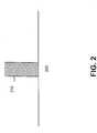
- processingmay begin by forming a dielectric fin structure 210 on a substrate 200 of a semiconductor device (act 105 ).
- substrate 200may comprise silicon.
- substrate 200may comprise other semiconducting materials, such as germanium, or combinations of semiconducting materials, such as silicon-germanium.
- substrate 200may include an insulator, such as an oxide layer, formed on a silicon or germanium substrate.
- Dielectric fin structure 210may comprise a dielectric material that causes significant tensile stress (strain) in the dual fin structures that will be formed adjacent dielectric fin structure 210 .
- dielectric fin structure 210may comprise an oxide or a nitride.
- Dielectric fin structure 210may be formed in a conventional manner. For example, a dielectric material may be deposited over substrate 200 toga thickness ranging from about 200 ⁇ to about 1000 ⁇ . A mask may be formed over a portion of the dielectric material and the dielectric material may then be etched in a conventional manner, with the etching terminating on substrate 200 to form dielectric fin structure 210 . The resulting dielectric fin structure 210 may have a width ranging from about 100 ⁇ to about 1000 ⁇ .
- an amorphous silicon layer 310may be deposited on the semiconductor device, as illustrated in FIG. 3 (act 110 ). In one implementation consistent with the principles of the invention, amorphous silicon layer 310 may be deposited to a thickness ranging from about 100 ⁇ to about 1000 ⁇ .
- Amorphous silicon layer 310may then be etched in a conventional manner, with the etching terminating at substrate 200 to form amorphous silicon spacer (fin) structures 410 , as illustrated in FIG. 4 (act 115 ).
- Each amorphous silicon fin structure 410may have a height ranging from about 200 ⁇ to about 1000 ⁇ and a width ranging from about 100 ⁇ to about 1000 ⁇ .
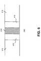
- a dielectric layer 510may be deposited on the semiconductor device, as illustrated in FIG. 5. (act 120 ). In one implementation consistent with the principles of the invention, dielectric layer 510 may be deposited to a thickness ranging from about 200 ⁇ to about 1000 ⁇ . Dielectric layer 510 may comprise an oxide or other dielectric materials.
- the semiconductor devicemay be polished via a chemical-mechanical polishing (CMP) (or other technique) to planarize the top surface of the semiconductor device such that the top surface of each of amorphous silicon fin structures 410 is exposed, as illustrated in FIG. 6 (act 120 ).
- CMPchemical-mechanical polishing
- a portion of the upper surface of dielectric fin structure 210 and amorphous silicon fin structures 410may be removed so that the upper surface of each of amorphous silicon fin structures 410 is exposed.
- the height of fins 210 and 410may range from abou 5 150 ⁇ to about 200 ⁇ .
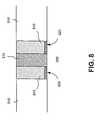
- a metal layer 710such as nickel, may be deposited on the semiconductor device, as illustrated in FIG. 7 (act 125 ).
- nickel layer 710may be deposited to a thickness of about 20 ⁇ .
- a metal-induced crystallization (MIC) operationmay then be performed.
- the MIC operationmay involve annealing nickel layer 710 at about 500° C. to about 550° C. for several hours, which acts to diffuse the nickel into the amorphous silicon to convert the amorphous silicon in fin structures 410 to single-crystal silicon 810 , as illustrated in FIG. 8 (act 130 ).
- a thin layer of a nickel silicon (NiSi) compound 820may formed between substrate 200 and single-crystal silicon fin structures 810 .
- the thickness of NiSi layer 820may range from about 20 ⁇ to about 200 ⁇ .
- single-crystal silicon fin structures 810are formed, conventional FinFET fabrication processing can be utilized to complete the transistor (e.g., forming the source and drain regions), contacts, interconnects and inter-level dielectrics for the FinFET device.
- dielectric layer 510may be removed, a protective dielectric layer, such as a silicon nitride or silicon oxide may be formed on the top surface of fins 210 and 810 , followed by the formation of a gate dielectric on the side surfaces of single-crystal silicon fin structures 810 .
- Source/drain regionsmay then be formed at the respective ends of fins 210 and 810 , followed by formation of one or more gates.
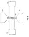
- FIG. 9illustrates an exemplary top view of the semiconductor device consistent with the principles of the invention after the source/drain regions and gate electrodes are formed.
- the semiconductor deviceincludes a double-gate structure with fins 210 and 810 , source and drain regions 910 and 920 , and gate electrodes 930 and 940 .
- Source/drain regions 910 and 920may then be doped with n-type or p-type impurities based on the particular end device requirements.
- sidewall spacersmay optionally be formed prior to the source/drain ion implantation to control the location of the source/drain junctions based on the particular circuit requirements.
- Activation annealingmay then be performed to activate source/drain regions 910 and 920 .
- single-crystal silicon fin structuresmay be formed, having a dielectric fin structure located between the single-crystal silicon fin structures.
- the material for the dielectric fin structuremay be chosen so as to induce a significant stress (strain) in the single-crystal silicon fin structures.
- strainsignificant stress
- FIGS. 10-15illustrate exemplary views for forming multiple fin structures in an alternative implementation consistent with the principles of the invention.
- processingmay begin with a semiconductor device that includes an oxide layer 1010 formed on a substrate 1000 .
- Substrate 1000may comprise silicon or other semiconducting materials, such as germanium, or combinations of semiconducting materials, such as silicon-germanium.
- Oxide layer 1010may have a height ranging from about 200 ⁇ to about 1000 ⁇ .
- Oxide layer 1010may be etched to form a trench 1020 , as illustrated in FIG. 10.
- trench 1020may have a width ranging from about 200 ⁇ to about 2000 ⁇ .
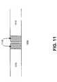
- amorphous siliconmay be deposited and etched to form amorphous silicon spacers 1110 , as illustrated in FIG. 11.
- Each of amorphous silicon spacers 1110may have a width ranging from about 100 ⁇ to about 1000 ⁇ .
- a dielectric material 1210may be deposited in the gap between amorphous silicon spacers 1110 , as illustrated in FIG. 12.
- the dielectric materialmay comprise an oxide or other dielectric materials.
- a layer of nickel 1310may deposited on a top surface of amorphous silicon spacers 1110 , as illustrated in FIG. 13.
- the thickness of nickel layer 1310may be about 20 ⁇ .
- a MIC operationmay then be performed.
- the MIC operationmay involve annealing nickel layer 1310 at about 500° C. to about 550° C. for several hours to convert amorphous silicon spacers 1110 to single-crystal silicon fin structures 1410 , as illustrated in FIG. 14.
- a thin layer of a nickel silicon (NiSi) compound 1420may be formed between substrate 1000 and single-crystal silicon fin structures 1410 .
- the thickness of NiSi layer 1420may range from about 20 ⁇ to about 200 ⁇ .
- Oxide layer 1010may then be removed in a conventional manner, as illustrated in FIG. 15. Accordingly, a spacer-induced merged FET can be produced.
- spacersmay be used to create a narrow trench that can provide a coupling effect between both sides of the trench.
- a semiconductor devicemay include an oxide layer 1610 formed on a substrate (not shown) with a silicon layer 1620 formed thereon.
- a materialsuch as a silicon nitride or a silicon oxide, may be deposited and patterned to form hard masks 1640 .
- a spacer materialsuch as SiN, SiO, or some other material, may be deposited and etched to form spacers 1630 on the side surfaces of hard masks 1640 .
- Silicon layer 1620may then be etched using spacers 1630 and hard masks 1640 as masks to form a narrow trench 1710 , as illustrated in FIG. 17.
- Trench 1710may have a width ranging from about 100 ⁇ to about 1000 ⁇ . Trench 1710 advantageously provides a coupling effect between fins 1620 located on both sides of trench 1710 .
- Implementations consistent with the principles of the inventionprovide single-crystal silicon fin structures that are formed on opposite sides of a dielectric fin structure.
- the material for the dielectric fin structureis chosen such that a significant stress is induced in the single-crystal silicon material. In this manner, enhanced mobility can be achieved.
Landscapes
- Engineering & Computer Science (AREA)
- Physics & Mathematics (AREA)
- Condensed Matter Physics & Semiconductors (AREA)
- General Physics & Mathematics (AREA)
- Manufacturing & Machinery (AREA)
- Computer Hardware Design (AREA)
- Microelectronics & Electronic Packaging (AREA)
- Power Engineering (AREA)
- Thin Film Transistor (AREA)
- Insulated Gate Type Field-Effect Transistor (AREA)
- Metal-Oxide And Bipolar Metal-Oxide Semiconductor Integrated Circuits (AREA)
- Recrystallisation Techniques (AREA)
Abstract
Description
- The present invention relates generally to semiconductor manufacturing and, more particularly, to forming FinFET devices.[0001]
- The escalating demands for high density and performance associated with ultra large scale integration semiconductor devices require design features, such as gate lengths, below 100 nanometers (nm), high reliability and increased manufacturing throughput. The reduction of design features below 100 nm challenges the limitations of conventional methodology.[0002]
- For example, when the gate length of conventional planar metal oxide semiconductor field effect transistors (MOSFETs) is scaled below 100 nm, problems associated with short channel effects, such as excessive leakage between the source and drain, become increasingly difficult to overcome. In addition, mobility degradation and a number of process issues also make it difficult to scale conventional MOSFETs to include increasingly smaller device features. New device structures are therefore being explored to improve FET performance and allow further device scaling.[0003]
- Double-gate MOSFETs represent new structures that have been considered as candidates for succeeding existing planar MOSFETs. In double-gate MOSFETs, two gates may be used to control short channel effects. A FinFET is a double-gate structure that exhibits good short channel behavior. A FinFET includes a channel formed in a vertical fin. The FinFET structure may also be fabricated using layout and process techniques similar to those used for conventional planar MOSFETs.[0004]
- Implementations consistent with the principles of the invention provide single-crystal silicon fin structures formed on opposite sides of a dielectric fin structure. The material for the dielectric fin structure is chosen such that a significant stress is induced in the single-crystal silicon material. Accordingly, enhanced mobility can be achieved.[0005]
- In accordance with the purpose of this invention as embodied and broadly described herein, a semiconductor device includes a first fin structure that comprises a dielectric material and includes a first side surface and a second side surface; a second fin structure that comprises a single-crystal silicon material and is formed adjacent to the first side surface of the first fin structure; a third fin structure that comprises the single-crystal silicon material and is formed adjacent to the second side surface of the first fin structure; a source region that is formed at one end of the first fin structure, the second fin structure, and the third fin structure; a drain region that is formed at an opposite end of the first fin structure, the second fin structure, and the third fin structure; and at least one gate.[0006]
- In another implementation consistent with the present invention, a method of manufacturing a semiconductor device that includes a substrate and a dielectric layer formed on the substrate is disclosed. The method includes etching the dielectric layer to form a first fin structure; depositing an amorphous silicon layer; etching the amorphous silicon layer to form a second fin structure adjacent a first side surface of the first fin structure and a third fin structure adjacent a second, opposite side surface of the first fin structure; depositing a metal layer on at least upper surfaces of the second fin structure and the third fin structure; performing a metal-induced crystallization operation to convert the amorphous silicon in the second and third fin structures to a single-crystal silicon material; forming a source region and a drain region; depositing a gate material over the first, second, and third fin structures; and patterning and etching the gate material to form at least one gate electrode.[0007]
- In yet another implementation consistent with the principles of the invention, a semiconductor device that includes a first fin structure, a second fin structure, and a third fin structure disclosed. The first and second fin structures include a single-crystal silicon material. The third fin structure is located between the first fin structure and the second fin structure and includes a dielectric material. The third fin structure causes stress to be induced in the single-crystal silicon material of the first fin structure and the second fin structure.[0008]
- The accompanying drawings, which are incorporated in and constitute a part of this specification, illustrate an embodiment of the invention and, together with the description, explain the invention. In the drawings,[0009]
- FIG. 1 illustrates an exemplary process for forming fin structures for a FinFET device in an implementation consistent with the principles of the invention;[0010]
- FIGS. 2-9 illustrate exemplary views of a FinFET device fabricated according to the processing described in FIG. 1;[0011]
- FIGS. 10-15 illustrate exemplary views for forming multiple fin structures in an alternative implementation consistent with the principles of the invention; and[0012]
- FIGS. 16 and 17 illustrate exemplary views for creating a trench according to an alternative implementation consistent with the principles of the invention.[0013]
- The following detailed description of implementations consistent with the present invention refers to the accompanying drawings. The same reference numbers in different drawings may identify the same or similar elements. Also, the following detailed description does not limit the invention. Instead, the scope of the invention is defined by the appended claims their equivalents.[0014]
- Implementations consistent with the principles of the invention provide single-crystal silicon fin structures that are formed on opposite sides of a dielectric fin structure. The material for the dielectric fin structure is chosen such that a significant stress is induced in the single-crystal silicon material to enhance mobility.[0015]
- FIG. 1 illustrates an exemplary process for forming fin structures for a FinFET device in an implementation consistent with the principles of the invention. FIGS. 2-9 illustrate exemplary views of a FinFET device fabricated according to the processing described in FIG. 1. The fabrication of one FinFET device will be described hereinafter. It will be appreciated, however, that the techniques described herein are equally applicable to forming more than one FinFET device.[0016]
- With reference to FIGS. 1 and 2, processing may begin by forming a[0017]
dielectric fin structure 210 on asubstrate 200 of a semiconductor device (act105). In one implementation,substrate 200 may comprise silicon. In alternative implementations consistent with the present invention,substrate 200 may comprise other semiconducting materials, such as germanium, or combinations of semiconducting materials, such as silicon-germanium. In another alternative,substrate 200 may include an insulator, such as an oxide layer, formed on a silicon or germanium substrate.Dielectric fin structure 210 may comprise a dielectric material that causes significant tensile stress (strain) in the dual fin structures that will be formed adjacentdielectric fin structure 210. In one implementation,dielectric fin structure 210 may comprise an oxide or a nitride. - [0018]
Dielectric fin structure 210 may be formed in a conventional manner. For example, a dielectric material may be deposited oversubstrate 200 toga thickness ranging from about 200 Å to about 1000 Å. A mask may be formed over a portion of the dielectric material and the dielectric material may then be etched in a conventional manner, with the etching terminating onsubstrate 200 to formdielectric fin structure 210. The resultingdielectric fin structure 210 may have a width ranging from about 100 Å to about 1000 Å. - After forming[0019]
dielectric fin structure 210, anamorphous silicon layer 310 may be deposited on the semiconductor device, as illustrated in FIG. 3 (act110). In one implementation consistent with the principles of the invention,amorphous silicon layer 310 may be deposited to a thickness ranging from about 100 Å to about 1000 Å. - [0020]
Amorphous silicon layer 310 may then be etched in a conventional manner, with the etching terminating atsubstrate 200 to form amorphous silicon spacer (fin)structures 410, as illustrated in FIG. 4 (act115). Each amorphous siliconfin structure 410 may have a height ranging from about 200 Å to about 1000 Å and a width ranging from about 100 Å to about 1000 Å. - A[0021]
dielectric layer 510 may be deposited on the semiconductor device, as illustrated in FIG. 5. (act120). In one implementation consistent with the principles of the invention,dielectric layer 510 may be deposited to a thickness ranging from about 200 Å to about 1000 Å.Dielectric layer 510 may comprise an oxide or other dielectric materials. - The semiconductor device may be polished via a chemical-mechanical polishing (CMP) (or other technique) to planarize the top surface of the semiconductor device such that the top surface of each of amorphous[0022]
silicon fin structures 410 is exposed, as illustrated in FIG. 6 (act120). During the CMP, a portion of the upper surface ofdielectric fin structure 210 and amorphoussilicon fin structures 410 may be removed so that the upper surface of each of amorphoussilicon fin structures 410 is exposed. For example, after the CMP, the height offins - A[0023]
metal layer 710, such as nickel, may be deposited on the semiconductor device, as illustrated in FIG. 7 (act125). In one implementation,nickel layer 710 may be deposited to a thickness of about 20 Å. - A metal-induced crystallization (MIC) operation may then be performed. The MIC operation may involve annealing[0024]
nickel layer 710 at about 500° C. to about 550° C. for several hours, which acts to diffuse the nickel into the amorphous silicon to convert the amorphous silicon infin structures 410 to single-crystal silicon 810, as illustrated in FIG. 8 (act130). As a result of the MIC operation, a thin layer of a nickel silicon (NiSi)compound 820 may formed betweensubstrate 200 and single-crystalsilicon fin structures 810. In one implementation, the thickness ofNiSi layer 820 may range from about 20 Å to about 200 Å. - After single-crystal[0025]
silicon fin structures 810 are formed, conventional FinFET fabrication processing can be utilized to complete the transistor (e.g., forming the source and drain regions), contacts, interconnects and inter-level dielectrics for the FinFET device. For example,dielectric layer 510 may be removed, a protective dielectric layer, such as a silicon nitride or silicon oxide may be formed on the top surface offins silicon fin structures 810. Source/drain regions may then be formed at the respective ends offins fins regions gate electrodes - Source/[0026]
drain regions drain regions - The present invention has been described above as forming a number of fin structures. It should be understood that methods consistent with the present invention may be used to form any number of fins, based on the particular circuit requirements.[0027]
- Thus, in accordance with the principles of the invention, single-crystal silicon fin structures may be formed, having a dielectric fin structure located between the single-crystal silicon fin structures. The material for the dielectric fin structure may be chosen so as to induce a significant stress (strain) in the single-crystal silicon fin structures. As a result, enhanced mobility in the single-crystal silicon fin structures is achieved.[0028]
- FIGS. 10-15 illustrate exemplary views for forming multiple fin structures in an alternative implementation consistent with the principles of the invention. With reference to FIG. 10, processing may begin with a semiconductor device that includes an[0029]
oxide layer 1010 formed on asubstrate 1000.Substrate 1000 may comprise silicon or other semiconducting materials, such as germanium, or combinations of semiconducting materials, such as silicon-germanium.Oxide layer 1010 may have a height ranging from about 200 Å to about 1000 Å. - [0030]
Oxide layer 1010 may be etched to form atrench 1020, as illustrated in FIG. 10. In one implementation,trench 1020 may have a width ranging from about 200 Å to about 2000 Å. Next, amorphous silicon may be deposited and etched to formamorphous silicon spacers 1110, as illustrated in FIG. 11. Each ofamorphous silicon spacers 1110 may have a width ranging from about 100 Å to about 1000 Å. Adielectric material 1210 may be deposited in the gap betweenamorphous silicon spacers 1110, as illustrated in FIG. 12. The dielectric material may comprise an oxide or other dielectric materials. - A layer of[0031]
nickel 1310 may deposited on a top surface ofamorphous silicon spacers 1110, as illustrated in FIG. 13. The thickness ofnickel layer 1310 may be about 20 Å. A MIC operation may then be performed. The MIC operation may involve annealingnickel layer 1310 at about 500° C. to about 550° C. for several hours to convertamorphous silicon spacers 1110 to single-crystalsilicon fin structures 1410, as illustrated in FIG. 14. As a result of the MIC operation, a thin layer of a nickel silicon (NiSi)compound 1420 may be formed betweensubstrate 1000 and single-crystalsilicon fin structures 1410. In one implementation, the thickness ofNiSi layer 1420 may range from about 20 Å to about 200 Å. - [0032]
Oxide layer 1010 may then be removed in a conventional manner, as illustrated in FIG. 15. Accordingly, a spacer-induced merged FET can be produced. - In another implementation, spacers may be used to create a narrow trench that can provide a coupling effect between both sides of the trench. As illustrated in FIG. 16, a semiconductor device may include an[0033]
oxide layer 1610 formed on a substrate (not shown) with asilicon layer 1620 formed thereon. A material, such as a silicon nitride or a silicon oxide, may be deposited and patterned to form hard masks1640. Next, a spacer material, such as SiN, SiO, or some other material, may be deposited and etched to formspacers 1630 on the side surfaces ofhard masks 1640.Silicon layer 1620 may then be etched usingspacers 1630 andhard masks 1640 as masks to form anarrow trench 1710, as illustrated in FIG. 17.Trench 1710 may have a width ranging from about 100 Å to about 1000 Å.Trench 1710 advantageously provides a coupling effect betweenfins 1620 located on both sides oftrench 1710. - Implementations consistent with the principles of the invention provide single-crystal silicon fin structures that are formed on opposite sides of a dielectric fin structure. The material for the dielectric fin structure is chosen such that a significant stress is induced in the single-crystal silicon material. In this manner, enhanced mobility can be achieved.[0034]
- The foregoing description of exemplary embodiments of the present invention provides illustration and description, but is not intended to be exhaustive or to limit the invention to the precise form disclosed. Modifications and variations are possible in light of the above teachings or may be acquired from practice of the invention. For example, in the above descriptions, numerous specific details are set forth, such as specific materials, structures, chemicals, processes, etc., in order to provide a thorough understanding of the present invention. However, the present invention can be practiced without resorting to the details specifically set forth herein. In other instances, well known processing structures have not been described in detail, in order not to unnecessarily obscure the thrust of the present invention. In practicing the present invention, conventional deposition, photolithographic and etching techniques may be employed, and hence, the details of such techniques have not been set forth herein in detail.[0035]
- While a series of acts has been described with regard to FIG. 1, the order of the acts may be varied in other implementations consistent with the present invention. Moreover, non-dependent acts may be implemented in parallel.[0036]
- No element, act, or instruction used in the description of the present application should be construed as critical or essential to the invention unless explicitly described as such. Also, as used herein, the article “a” is intended to include one or more items. Where only one item is intended, the term “one” or similar language is used.[0037]
- The scope of the invention is defined by the claims and their equivalents.[0038]
Claims (22)
1-4. (canceled)
5. A method of manufacturing a semiconductor device that includes a substrate and a dielectric layer formed on the substrate, the method comprising:
etching the dielectric layer to form a first fin structure;
depositing an amorphous silicon layer;
etching the amorphous silicon layer to form a second fin structure adjacent a first side surface of the first fin structure and a third fin structure adjacent a second, opposite side surface of the first fin structure;
depositing a metal layer on at least upper surfaces of the second fin structure and the third fin structure;
performing a metal-induced crystallization operation to convert the amorphous silicon in the second and third fin structures to a single-crystal silicon material;
forming a source region and a drain region;
depositing a gate material over the first, second, and third fin structures; and
patterning and etching the gate material to form at least one gate electrode.
6. The method ofclaim 5 wherein a width of the first fin structure ranges from about 200 Å to about 1000 Å.
7. The method ofclaim 5 wherein the dielectric layer comprises at least an oxide or a nitride.
8. The method ofclaim 5 wherein a width of each of the second fin structure and the third fin structure ranges from about 100 Å to about 1000 Å.
9. The method ofclaim 5 further comprising:
forming a second dielectric layer prior to depositing the metal layer; and
planarizing the second dielectric layer to expose upper surfaces of the second fin structure and the third fin structure.
10. The method ofclaim 5 wherein the performing a metal-induced crystallization operation forms a metal-silicon compound at a bottom surface of each of the second fin structure and the third fin structure.
11. The method ofclaim 10 wherein a thickness of the metal-silicon compound ranges from about 20 Å to about 200 Å.
12. The method ofclaim 5 wherein the depositing a metal layer includes:
depositing a nickel layer to a thickness of about 20 Å.
13. The method ofclaim 5 wherein the performing includes:
annealing the second fin structure and the third fin structure at a temperature of about 500° C. to about 550° C.
14. The method ofclaim 13 wherein the annealing is performed for at least two hours.
15-19. (canceled)
20. A method for forming fin structures for a semiconductor device, comprising:
forming a first fin structure comprising a dielectric material and including a first side surface and a second side surface;
forming a second fin structure adjacent the first side surface of the first fin structure; and
forming a third fin structure adjacent the second side surface of the first fin structure, the second fin structure and the third fin structure being formed of a different material than the first fin structure.
21. The method ofclaim 20 wherein the forming a first fin structure includes:
forming the first fin structure to a width ranging from about 200 Å to about 1000 Å.
22. The method ofclaim 20 wherein the dielectric material includes an oxide or a nitride.
23. The method ofclaim 20 wherein the forming a second fin structure includes:
forming the second fin structure to a width ranging from about 100 Å to about 1000 Å, and
wherein the forming the third fin structure includes:
forming the third fin structure to a width ranging from about 100 Å to about 1000 Å.
24. The method ofclaim 20 wherein the forming the second fin structure and the third fin structure includes:
depositing an amorphous silicon layer, and
etching the amorphous silicon layer to form the second fin structure adjacent the first side surface of the first fin structure and the third fin structure adjacent the second side surface of the first fin structure.
25. The method ofclaim 24 further comprising:
depositing a metal layer on at least upper surfaces of the second fin structure and the third fin structure; and
performing a metal-induced crystallization operation to convert the amorphous silicon in the second and third fin structures to a single-crystal silicon material.
26. A method for forming fin structures for a semiconductor device that includes a substrate and a dielectric layer formed on the substrate, the method comprising:
etching the dielectric layer to form a first fin structure;
depositing an amorphous silicon layer; and
etching the amorphous silicon layer to form a second fin structure adjacent a first side surface of the first fin structure and a third fin structure adjacent a second, opposite side surface of the first fin structure.
27. The method ofclaim 26 further comprising:
depositing a metal layer on at least upper surfaces of the second fin structure and the third fin structure; and
performing a metal-induced crystallization operation to convert the amorphous silicon in the second and third fin structures to a single-crystal silicon material.
28. The method ofclaim 26 wherein the etching the dielectric layer includes:
forming the first fin structure to a width ranging from about 200 Å to about 1000 Å, and
wherein the etching the amorphous silicon layer includes:
forming the second fin structure to a width ranging from about 100 Å to about 1000 Å, and
forming the third fin structure to a width ranging from about 100 Å to about 1000 Å.
29. The method ofclaim 26 wherein the dielectric material includes an oxide or a nitride.
Priority Applications (1)
| Application Number | Priority Date | Filing Date | Title |
|---|---|---|---|
| US10/825,175US6852576B2 (en) | 2003-04-03 | 2004-04-16 | Method for forming structures in finfet devices |
Applications Claiming Priority (2)
| Application Number | Priority Date | Filing Date | Title |
|---|---|---|---|
| US10/405,343US6762448B1 (en) | 2003-04-03 | 2003-04-03 | FinFET device with multiple fin structures |
| US10/825,175US6852576B2 (en) | 2003-04-03 | 2004-04-16 | Method for forming structures in finfet devices |
Related Parent Applications (1)
| Application Number | Title | Priority Date | Filing Date |
|---|---|---|---|
| US10/405,343DivisionUS6762448B1 (en) | 2003-04-03 | 2003-04-03 | FinFET device with multiple fin structures |
Publications (2)
| Publication Number | Publication Date |
|---|---|
| US20040198031A1true US20040198031A1 (en) | 2004-10-07 |
| US6852576B2 US6852576B2 (en) | 2005-02-08 |
Family
ID=32681857
Family Applications (2)
| Application Number | Title | Priority Date | Filing Date |
|---|---|---|---|
| US10/405,343Expired - LifetimeUS6762448B1 (en) | 2003-04-03 | 2003-04-03 | FinFET device with multiple fin structures |
| US10/825,175Expired - LifetimeUS6852576B2 (en) | 2003-04-03 | 2004-04-16 | Method for forming structures in finfet devices |
Family Applications Before (1)
| Application Number | Title | Priority Date | Filing Date |
|---|---|---|---|
| US10/405,343Expired - LifetimeUS6762448B1 (en) | 2003-04-03 | 2003-04-03 | FinFET device with multiple fin structures |
Country Status (8)
| Country | Link |
|---|---|
| US (2) | US6762448B1 (en) |
| JP (1) | JP5009611B2 (en) |
| KR (1) | KR101070845B1 (en) |
| CN (1) | CN100413038C (en) |
| DE (1) | DE112004000586B4 (en) |
| GB (1) | GB2417829B (en) |
| TW (1) | TWI384614B (en) |
| WO (1) | WO2004093197A2 (en) |
Cited By (9)
| Publication number | Priority date | Publication date | Assignee | Title |
|---|---|---|---|---|
| US20060148226A1 (en)* | 2004-12-31 | 2006-07-06 | Dongbuanam Semiconductor Inc. | Method of forming fine patterns in semiconductor device and method of forming gate using the same |
| US7101763B1 (en) | 2005-05-17 | 2006-09-05 | International Business Machines Corporation | Low capacitance junction-isolation for bulk FinFET technology |
| US20060197147A1 (en)* | 2005-02-24 | 2006-09-07 | International Business Machines Corporation | Improved double gate isolation |
| US20070063230A1 (en)* | 2005-09-19 | 2007-03-22 | International Business Machines Corporation | Asymmetrically stressed cmos finfet |
| US20080164535A1 (en)* | 2007-01-09 | 2008-07-10 | Dureseti Chidambarrao | Curved finfets |
| US7936003B2 (en) | 2005-02-03 | 2011-05-03 | Samsung Electronics Co., Ltd. | Semiconductor device having transistor with vertical gate electrode and method of fabricating the same |
| US20140225168A1 (en)* | 2013-02-11 | 2014-08-14 | Globalfoundries Inc. | Methods of forming a three-dimensional semiconductor device with a dual stress channel and the resulting device |
| US9722052B2 (en)* | 2015-10-27 | 2017-08-01 | International Business Machines Corporation | Fin cut without residual fin defects |
| US9905694B2 (en)* | 2016-07-20 | 2018-02-27 | Globalfoundries Inc. | Fin-type field-effect transistors with strained channels |
Families Citing this family (87)
| Publication number | Priority date | Publication date | Assignee | Title |
|---|---|---|---|---|
| US6709982B1 (en)* | 2002-11-26 | 2004-03-23 | Advanced Micro Devices, Inc. | Double spacer FinFET formation |
| US7105894B2 (en)* | 2003-02-27 | 2006-09-12 | Taiwan Semiconductor Manufacturing Co., Ltd. | Contacts to semiconductor fin devices |
| US6900502B2 (en) | 2003-04-03 | 2005-05-31 | Taiwan Semiconductor Manufacturing Company, Ltd. | Strained channel on insulator device |
| US6882025B2 (en)* | 2003-04-25 | 2005-04-19 | Taiwan Semiconductor Manufacturing Company, Ltd. | Strained-channel transistor and methods of manufacture |
| US7074656B2 (en)* | 2003-04-29 | 2006-07-11 | Taiwan Semiconductor Manufacturing Company, Ltd. | Doping of semiconductor fin devices |
| US6867433B2 (en) | 2003-04-30 | 2005-03-15 | Taiwan Semiconductor Manufacturing Company, Ltd. | Semiconductor-on-insulator chip incorporating strained-channel partially-depleted, fully-depleted, and multiple-gate transistors |
| US6909147B2 (en)* | 2003-05-05 | 2005-06-21 | International Business Machines Corporation | Multi-height FinFETS |
| KR100521382B1 (en)* | 2003-06-30 | 2005-10-12 | 삼성전자주식회사 | Method for fabricating a finfet in a semiconductor device |
| US6943405B2 (en)* | 2003-07-01 | 2005-09-13 | International Business Machines Corporation | Integrated circuit having pairs of parallel complementary FinFETs |
| US20050012087A1 (en)* | 2003-07-15 | 2005-01-20 | Yi-Ming Sheu | Self-aligned MOSFET having an oxide region below the channel |
| US6940705B2 (en) | 2003-07-25 | 2005-09-06 | Taiwan Semiconductor Manufacturing Company, Ltd. | Capacitor with enhanced performance and method of manufacture |
| US7078742B2 (en)* | 2003-07-25 | 2006-07-18 | Taiwan Semiconductor Manufacturing Co., Ltd. | Strained-channel semiconductor structure and method of fabricating the same |
| US6936881B2 (en)* | 2003-07-25 | 2005-08-30 | Taiwan Semiconductor Manufacturing Company, Ltd. | Capacitor that includes high permittivity capacitor dielectric |
| JP3860582B2 (en)* | 2003-07-31 | 2006-12-20 | 株式会社東芝 | Manufacturing method of semiconductor device |
| US7301206B2 (en)* | 2003-08-01 | 2007-11-27 | Taiwan Semiconductor Manufacturing Company, Ltd. | Semiconductor-on-insulator SRAM configured using partially-depleted and fully-depleted transistors |
| US7101742B2 (en)* | 2003-08-12 | 2006-09-05 | Taiwan Semiconductor Manufacturing Company, Ltd. | Strained channel complementary field-effect transistors and methods of manufacture |
| US20050035410A1 (en)* | 2003-08-15 | 2005-02-17 | Yee-Chia Yeo | Semiconductor diode with reduced leakage |
| US20050035369A1 (en)* | 2003-08-15 | 2005-02-17 | Chun-Chieh Lin | Structure and method of forming integrated circuits utilizing strained channel transistors |
| US7112495B2 (en)* | 2003-08-15 | 2006-09-26 | Taiwan Semiconductor Manufacturing Company, Ltd. | Structure and method of a strained channel transistor and a second semiconductor component in an integrated circuit |
| US7071052B2 (en)* | 2003-08-18 | 2006-07-04 | Taiwan Semiconductor Manufacturing Company, Ltd. | Resistor with reduced leakage |
| US7888201B2 (en)* | 2003-11-04 | 2011-02-15 | Taiwan Semiconductor Manufacturing Company, Ltd. | Semiconductor-on-insulator SRAM configured using partially-depleted and fully-depleted transistors |
| US6962843B2 (en)* | 2003-11-05 | 2005-11-08 | International Business Machines Corporation | Method of fabricating a finfet |
| US7498225B1 (en)* | 2003-12-04 | 2009-03-03 | Advanced Micro Devices, Inc. | Systems and methods for forming multiple fin structures using metal-induced-crystallization |
| US7198995B2 (en)* | 2003-12-12 | 2007-04-03 | International Business Machines Corporation | Strained finFETs and method of manufacture |
| US20050186722A1 (en)* | 2004-02-25 | 2005-08-25 | Kuan-Lun Cheng | Method and structure for CMOS device with stress relaxed by ion implantation of carbon or oxygen containing ions |
| KR100605104B1 (en)* | 2004-05-04 | 2006-07-26 | 삼성전자주식회사 | Fin-Pet device and its manufacturing method |
| US20050266632A1 (en)* | 2004-05-26 | 2005-12-01 | Yun-Hsiu Chen | Integrated circuit with strained and non-strained transistors, and method of forming thereof |
| US7452778B2 (en)* | 2004-06-10 | 2008-11-18 | Taiwan Semiconductor Manufacturing Company, Ltd. | Semiconductor nano-wire devices and methods of fabrication |
| JP2006128494A (en)* | 2004-10-29 | 2006-05-18 | Toshiba Corp | Semiconductor integrated circuit device and manufacturing method thereof |
| US20060118892A1 (en)* | 2004-12-02 | 2006-06-08 | Taiwan Semiconductor Manufacturing Company, Ltd. | Methods and Structures to Produce a Strain-Inducing Layer in a Semiconductor Device |
| US20070018239A1 (en)* | 2005-07-20 | 2007-01-25 | International Business Machines Corporation | Sea-of-fins structure on a semiconductor substrate and method of fabrication |
| KR100642384B1 (en)* | 2005-09-15 | 2006-11-03 | 주식회사 하이닉스반도체 | Transistor of semiconductor memory device and manufacturing method thereof |
| FR2895835B1 (en)* | 2005-12-30 | 2008-05-09 | Commissariat Energie Atomique | ACHIEVING A MULTI-BRANCH CHANNEL STRUCTURE OF A TRANSISTOR GRID AND MEANS FOR ISOLATING THIS GRID FROM THE SOURCE AND DRAIN REGIONS |
| US8734583B2 (en)* | 2006-04-04 | 2014-05-27 | Micron Technology, Inc. | Grown nanofin transistors |
| US8354311B2 (en)* | 2006-04-04 | 2013-01-15 | Micron Technology, Inc. | Method for forming nanofin transistors |
| US7491995B2 (en) | 2006-04-04 | 2009-02-17 | Micron Technology, Inc. | DRAM with nanofin transistors |
| US7425491B2 (en) | 2006-04-04 | 2008-09-16 | Micron Technology, Inc. | Nanowire transistor with surrounding gate |
| US8558278B2 (en) | 2007-01-16 | 2013-10-15 | Taiwan Semiconductor Manufacturing Company, Ltd. | Strained transistor with optimized drive current and method of forming |
| FR2921757B1 (en)* | 2007-09-28 | 2009-12-18 | Commissariat Energie Atomique | DOUBLE-GRID TRANSISTOR STRUCTURE WITH MULTI-BRANCH CHANNEL |
| JP5193583B2 (en)* | 2007-12-17 | 2013-05-08 | 株式会社東芝 | Fin type transistor |
| US7943961B2 (en) | 2008-03-13 | 2011-05-17 | Taiwan Semiconductor Manufacturing Company, Ltd. | Strain bars in stressed layers of MOS devices |
| US7808051B2 (en) | 2008-09-29 | 2010-10-05 | Taiwan Semiconductor Manufacturing Company, Ltd. | Standard cell without OD space effect in Y-direction |
| US8305829B2 (en)* | 2009-02-23 | 2012-11-06 | Taiwan Semiconductor Manufacturing Company, Ltd. | Memory power gating circuit for controlling internal voltage of a memory array, system and method for controlling the same |
| US8305790B2 (en)* | 2009-03-16 | 2012-11-06 | Taiwan Semiconductor Manufacturing Company, Ltd. | Electrical anti-fuse and related applications |
| US8957482B2 (en)* | 2009-03-31 | 2015-02-17 | Taiwan Semiconductor Manufacturing Company, Ltd. | Electrical fuse and related applications |
| US8912602B2 (en)* | 2009-04-14 | 2014-12-16 | Taiwan Semiconductor Manufacturing Company, Ltd. | FinFETs and methods for forming the same |
| US8461015B2 (en)* | 2009-07-08 | 2013-06-11 | Taiwan Semiconductor Manufacturing Company, Ltd. | STI structure and method of forming bottom void in same |
| US8264032B2 (en)* | 2009-09-01 | 2012-09-11 | Taiwan Semiconductor Manufacturing Company, Ltd. | Accumulation type FinFET, circuits and fabrication method thereof |
| US8623728B2 (en)* | 2009-07-28 | 2014-01-07 | Taiwan Semiconductor Manufacturing Company, Ltd. | Method for forming high germanium concentration SiGe stressor |
| US8440517B2 (en) | 2010-10-13 | 2013-05-14 | Taiwan Semiconductor Manufacturing Company, Ltd. | FinFET and method of fabricating the same |
| US8264021B2 (en)* | 2009-10-01 | 2012-09-11 | Taiwan Semiconductor Manufacturing Company, Ltd. | Finfets and methods for forming the same |
| US9484462B2 (en)* | 2009-09-24 | 2016-11-01 | Taiwan Semiconductor Manufacturing Company, Ltd. | Fin structure of fin field effect transistor |
| US8629478B2 (en)* | 2009-07-31 | 2014-01-14 | Taiwan Semiconductor Manufacturing Company, Ltd. | Fin structure for high mobility multiple-gate transistor |
| US8497528B2 (en) | 2010-05-06 | 2013-07-30 | Taiwan Semiconductor Manufacturing Company, Ltd. | Method for fabricating a strained structure |
| US8759943B2 (en) | 2010-10-08 | 2014-06-24 | Taiwan Semiconductor Manufacturing Company, Ltd. | Transistor having notched fin structure and method of making the same |
| US8187928B2 (en) | 2010-09-21 | 2012-05-29 | Taiwan Semiconductor Manufacturing Company, Ltd. | Methods of forming integrated circuits |
| US8482073B2 (en)* | 2010-03-25 | 2013-07-09 | Taiwan Semiconductor Manufacturing Company, Ltd. | Integrated circuit including FINFETs and methods for forming the same |
| US8980719B2 (en) | 2010-04-28 | 2015-03-17 | Taiwan Semiconductor Manufacturing Company, Ltd. | Methods for doping fin field-effect transistors |
| US8298925B2 (en) | 2010-11-08 | 2012-10-30 | Taiwan Semiconductor Manufacturing Company, Ltd. | Mechanisms for forming ultra shallow junction |
| US8472227B2 (en)* | 2010-01-27 | 2013-06-25 | Taiwan Semiconductor Manufacturing Company, Ltd. | Integrated circuits and methods for forming the same |
| US20110097867A1 (en)* | 2009-10-22 | 2011-04-28 | Taiwan Semiconductor Manufacturing Company, Ltd. | Method of controlling gate thicknesses in forming fusi gates |
| US8021949B2 (en)* | 2009-12-01 | 2011-09-20 | International Business Machines Corporation | Method and structure for forming finFETs with multiple doping regions on a same chip |
| US9040393B2 (en) | 2010-01-14 | 2015-05-26 | Taiwan Semiconductor Manufacturing Company, Ltd. | Method of forming semiconductor structure |
| CN102263131B (en)* | 2010-05-25 | 2013-05-01 | 中国科学院微电子研究所 | Semiconductor device and forming method thereof |
| US8603924B2 (en) | 2010-10-19 | 2013-12-10 | Taiwan Semiconductor Manufacturing Company, Ltd. | Methods of forming gate dielectric material |
| US9048181B2 (en) | 2010-11-08 | 2015-06-02 | Taiwan Semiconductor Manufacturing Company, Ltd. | Mechanisms for forming ultra shallow junction |
| US8769446B2 (en) | 2010-11-12 | 2014-07-01 | Taiwan Semiconductor Manufacturing Company, Ltd. | Method and device for increasing fin device density for unaligned fins |
| US8592915B2 (en) | 2011-01-25 | 2013-11-26 | Taiwan Semiconductor Manufacturing Company, Ltd. | Doped oxide for shallow trench isolation (STI) |
| US8877602B2 (en) | 2011-01-25 | 2014-11-04 | Taiwan Semiconductor Manufacturing Company, Ltd. | Mechanisms of doping oxide for forming shallow trench isolation |
| US8431453B2 (en) | 2011-03-31 | 2013-04-30 | Taiwan Semiconductor Manufacturing Company, Ltd. | Plasma doping to reduce dielectric loss during removal of dummy layers in a gate structure |
| CN102956700B (en)* | 2011-08-30 | 2015-06-24 | 中国科学院微电子研究所 | Semiconductor structure and manufacturing method thereof |
| US8872284B2 (en) | 2012-03-20 | 2014-10-28 | Taiwan Semiconductor Manufacturing Company, Ltd. | FinFET with metal gate stressor |
| CN103378129B (en)* | 2012-04-19 | 2016-03-23 | 中国科学院微电子研究所 | Semiconductor structure and manufacturing method thereof |
| US8987790B2 (en) | 2012-11-26 | 2015-03-24 | International Business Machines Corporation | Fin isolation in multi-gate field effect transistors |
| US9396931B2 (en) | 2013-08-01 | 2016-07-19 | Qualcomm Incorporated | Method of forming fins from different materials on a substrate |
| US9548213B2 (en) | 2014-02-25 | 2017-01-17 | International Business Machines Corporation | Dielectric isolated fin with improved fin profile |
| US9224605B2 (en)* | 2014-05-01 | 2015-12-29 | Globalfoundries Inc. | Forming alternative material fins with reduced defect density by performing an implantation/anneal defect generation process |
| US9123627B1 (en)* | 2014-05-01 | 2015-09-01 | Globalfoundries Inc. | Methods of forming alternative material fins with reduced defect density for a FinFET semiconductor device |
| CN105097535B (en)* | 2014-05-12 | 2018-03-13 | 中国科学院微电子研究所 | method for manufacturing FinFet device |
| US9847329B2 (en)* | 2014-09-04 | 2017-12-19 | Taiwan Semiconductor Manufacturing Company, Ltd. | Structure of fin feature and method of making same |
| US9805991B2 (en)* | 2015-08-20 | 2017-10-31 | International Business Machines Corporation | Strained finFET device fabrication |
| US10103246B2 (en) | 2016-06-09 | 2018-10-16 | International Business Machines Corporation | Fabrication of a vertical fin field effect transistor (vertical finFET) with a self-aligned gate and fin edges |
| US9773870B1 (en) | 2016-06-28 | 2017-09-26 | International Business Machines Corporation | Strained semiconductor device |
| US10559501B2 (en)* | 2016-09-20 | 2020-02-11 | Qualcomm Incorporated | Self-aligned quadruple patterning process for Fin pitch below 20nm |
| FR3089343B1 (en)* | 2018-11-29 | 2021-10-08 | Commissariat Energie Atomique | PROCESS FOR MAKING A TRANSISTOR FET |
| US11011626B2 (en) | 2019-05-07 | 2021-05-18 | International Business Machines Corporation | Fin field-effect transistor with reduced parasitic capacitance and reduced variability |
| US11476356B2 (en) | 2020-05-29 | 2022-10-18 | Taiwan Semiconductor Manufacturing Co., Ltd. | Fin field-effect transistor device with low-dimensional material and method |
Citations (21)
| Publication number | Priority date | Publication date | Assignee | Title |
|---|---|---|---|---|
| US4996574A (en)* | 1988-07-01 | 1991-02-26 | Fujitsu Limited | MIS transistor structure for increasing conductance between source and drain regions |
| US5115289A (en)* | 1988-11-21 | 1992-05-19 | Hitachi, Ltd. | Semiconductor device and semiconductor memory device |
| US5338959A (en)* | 1992-03-30 | 1994-08-16 | Samsung Electronics Co., Ltd. | Thin film transistor with three dimensional multichannel structure |
| US5545586A (en)* | 1990-11-27 | 1996-08-13 | Nec Corporation | Method of making a transistor having easily controllable impurity profile |
| US5705414A (en)* | 1995-12-21 | 1998-01-06 | Siemens Aktiengesellschaft | Method for producing a gate electrode for an MOS structure |
| US5932911A (en)* | 1996-12-13 | 1999-08-03 | Advanced Micro Devices, Inc. | Bar field effect transistor |
| US6177299B1 (en)* | 1998-01-15 | 2001-01-23 | International Business Machines Corporation | Transistor having substantially isolated body and method of making the same |
| US6232622B1 (en)* | 1998-09-30 | 2001-05-15 | Sanyo Electric Co., Ltd. | Semiconductor device with high electric field effect mobility |
| US6358827B1 (en)* | 2001-01-19 | 2002-03-19 | Taiwan Semiconductor Manufacturing Company | Method of forming a squared-off, vertically oriented polysilicon spacer gate |
| US20020043690A1 (en)* | 1997-09-29 | 2002-04-18 | Doyle Brian S. | Fabrication of deep submicron structures and quantum wire transistors using hard-mask transistor width definition |
| US20020060338A1 (en)* | 2000-11-22 | 2002-05-23 | Zhibo Zhang | Methods of fabricating vertical field effect transistors by conformal channel layer deposition on sidewalls and vertical field effect transistors fabricated thereby |
| US6413802B1 (en)* | 2000-10-23 | 2002-07-02 | The Regents Of The University Of California | Finfet transistor structures having a double gate channel extending vertically from a substrate and methods of manufacture |
| US6492212B1 (en)* | 2001-10-05 | 2002-12-10 | International Business Machines Corporation | Variable threshold voltage double gated transistors and method of fabrication |
| US6514819B1 (en)* | 1996-03-01 | 2003-02-04 | Ace Memory, Inc. | High capacity stacked DRAM device and process for making a smaller geometry |
| US6537880B1 (en)* | 2001-09-13 | 2003-03-25 | Vanguard International Semiconductor Corporation | Method of fabricating a high density NAND stacked gate flash memory device having narrow pitch isolation and large capacitance between control and floating gates |
| US6562665B1 (en)* | 2000-10-16 | 2003-05-13 | Advanced Micro Devices, Inc. | Fabrication of a field effect transistor with a recess in a semiconductor pillar in SOI technology |
| US6583469B1 (en)* | 2002-01-28 | 2003-06-24 | International Business Machines Corporation | Self-aligned dog-bone structure for FinFET applications and methods to fabricate the same |
| US6645797B1 (en)* | 2002-12-06 | 2003-11-11 | Advanced Micro Devices, Inc. | Method for forming fins in a FinFET device using sacrificial carbon layer |
| US6657259B2 (en)* | 2001-12-04 | 2003-12-02 | International Business Machines Corporation | Multiple-plane FinFET CMOS |
| US6770516B2 (en)* | 2002-09-05 | 2004-08-03 | Taiwan Semiconductor Manufacturing Company | Method of forming an N channel and P channel FINFET device on the same semiconductor substrate |
| US6794718B2 (en)* | 2002-12-19 | 2004-09-21 | International Business Machines Corporation | High mobility crystalline planes in double-gate CMOS technology |
Family Cites Families (17)
| Publication number | Priority date | Publication date | Assignee | Title |
|---|---|---|---|---|
| JPH04250667A (en)* | 1991-01-28 | 1992-09-07 | Oki Electric Ind Co Ltd | Semiconductor device and manufacture thereof |
| JP2789931B2 (en)* | 1991-05-27 | 1998-08-27 | 日本電気株式会社 | Semiconductor device |
| KR920022546A (en)* | 1991-05-31 | 1992-12-19 | 김광호 | Structure of MOS transistor and its manufacturing method |
| JPH04354138A (en)* | 1991-05-31 | 1992-12-08 | Oki Electric Ind Co Ltd | Manufacture of mis type semiconductor device |
| JP3203048B2 (en)* | 1992-04-21 | 2001-08-27 | 三菱電機株式会社 | Semiconductor device and method of manufacturing the same |
| JPH09293793A (en)* | 1996-04-26 | 1997-11-11 | Mitsubishi Electric Corp | Semiconductor device having thin film transistor and manufacturing method thereof |
| JP2001185721A (en)* | 1999-12-22 | 2001-07-06 | Nec Corp | Semiconductor device |
| US6483156B1 (en)* | 2000-03-16 | 2002-11-19 | International Business Machines Corporation | Double planar gated SOI MOSFET structure |
| US20020011612A1 (en) | 2000-07-31 | 2002-01-31 | Kabushiki Kaisha Toshiba | Semiconductor device and method for manufacturing the same |
| JP4044276B2 (en) | 2000-09-28 | 2008-02-06 | 株式会社東芝 | Semiconductor device and manufacturing method thereof |
| US7163864B1 (en)* | 2000-10-18 | 2007-01-16 | International Business Machines Corporation | Method of fabricating semiconductor side wall fin |
| US6475869B1 (en)* | 2001-02-26 | 2002-11-05 | Advanced Micro Devices, Inc. | Method of forming a double gate transistor having an epitaxial silicon/germanium channel region |
| US6635909B2 (en) | 2002-03-19 | 2003-10-21 | International Business Machines Corporation | Strained fin FETs structure and method |
| EP1383164A1 (en)* | 2002-07-17 | 2004-01-21 | Interuniversitair Micro-Elektronica Centrum (IMEC) | FinFET device and a method for manufacturing such device |
| US7358121B2 (en) | 2002-08-23 | 2008-04-15 | Intel Corporation | Tri-gate devices and methods of fabrication |
| US6864519B2 (en) | 2002-11-26 | 2005-03-08 | Taiwan Semiconductor Manufacturing Co., Ltd. | CMOS SRAM cell configured using multiple-gate transistors |
| US6716686B1 (en) | 2003-07-08 | 2004-04-06 | Advanced Micro Devices, Inc. | Method for forming channels in a finfet device |
- 2003
- 2003-04-03USUS10/405,343patent/US6762448B1/ennot_activeExpired - Lifetime
- 2004
- 2004-03-29CNCNB2004800087527Apatent/CN100413038C/ennot_activeExpired - Lifetime
- 2004-03-29DEDE112004000586Tpatent/DE112004000586B4/ennot_activeExpired - Lifetime
- 2004-03-29JPJP2006509472Apatent/JP5009611B2/ennot_activeExpired - Lifetime
- 2004-03-29WOPCT/US2004/009696patent/WO2004093197A2/enactiveSearch and Examination
- 2004-03-29GBGB0521181Apatent/GB2417829B/ennot_activeExpired - Lifetime
- 2004-03-29KRKR1020057018827Apatent/KR101070845B1/ennot_activeExpired - Lifetime
- 2004-04-01TWTW093109021Apatent/TWI384614B/ennot_activeIP Right Cessation
- 2004-04-16USUS10/825,175patent/US6852576B2/ennot_activeExpired - Lifetime
Patent Citations (22)
| Publication number | Priority date | Publication date | Assignee | Title |
|---|---|---|---|---|
| US4996574A (en)* | 1988-07-01 | 1991-02-26 | Fujitsu Limited | MIS transistor structure for increasing conductance between source and drain regions |
| US5115289A (en)* | 1988-11-21 | 1992-05-19 | Hitachi, Ltd. | Semiconductor device and semiconductor memory device |
| US5545586A (en)* | 1990-11-27 | 1996-08-13 | Nec Corporation | Method of making a transistor having easily controllable impurity profile |
| US5338959A (en)* | 1992-03-30 | 1994-08-16 | Samsung Electronics Co., Ltd. | Thin film transistor with three dimensional multichannel structure |
| US5705414A (en)* | 1995-12-21 | 1998-01-06 | Siemens Aktiengesellschaft | Method for producing a gate electrode for an MOS structure |
| US6514819B1 (en)* | 1996-03-01 | 2003-02-04 | Ace Memory, Inc. | High capacity stacked DRAM device and process for making a smaller geometry |
| US5932911A (en)* | 1996-12-13 | 1999-08-03 | Advanced Micro Devices, Inc. | Bar field effect transistor |
| US6180441B1 (en)* | 1996-12-13 | 2001-01-30 | Advanced Micro Devices, Inc. | Bar field effect transistor |
| US20020043690A1 (en)* | 1997-09-29 | 2002-04-18 | Doyle Brian S. | Fabrication of deep submicron structures and quantum wire transistors using hard-mask transistor width definition |
| US6177299B1 (en)* | 1998-01-15 | 2001-01-23 | International Business Machines Corporation | Transistor having substantially isolated body and method of making the same |
| US6232622B1 (en)* | 1998-09-30 | 2001-05-15 | Sanyo Electric Co., Ltd. | Semiconductor device with high electric field effect mobility |
| US6562665B1 (en)* | 2000-10-16 | 2003-05-13 | Advanced Micro Devices, Inc. | Fabrication of a field effect transistor with a recess in a semiconductor pillar in SOI technology |
| US6413802B1 (en)* | 2000-10-23 | 2002-07-02 | The Regents Of The University Of California | Finfet transistor structures having a double gate channel extending vertically from a substrate and methods of manufacture |
| US20020060338A1 (en)* | 2000-11-22 | 2002-05-23 | Zhibo Zhang | Methods of fabricating vertical field effect transistors by conformal channel layer deposition on sidewalls and vertical field effect transistors fabricated thereby |
| US6358827B1 (en)* | 2001-01-19 | 2002-03-19 | Taiwan Semiconductor Manufacturing Company | Method of forming a squared-off, vertically oriented polysilicon spacer gate |
| US6537880B1 (en)* | 2001-09-13 | 2003-03-25 | Vanguard International Semiconductor Corporation | Method of fabricating a high density NAND stacked gate flash memory device having narrow pitch isolation and large capacitance between control and floating gates |
| US6492212B1 (en)* | 2001-10-05 | 2002-12-10 | International Business Machines Corporation | Variable threshold voltage double gated transistors and method of fabrication |
| US6657259B2 (en)* | 2001-12-04 | 2003-12-02 | International Business Machines Corporation | Multiple-plane FinFET CMOS |
| US6583469B1 (en)* | 2002-01-28 | 2003-06-24 | International Business Machines Corporation | Self-aligned dog-bone structure for FinFET applications and methods to fabricate the same |
| US6770516B2 (en)* | 2002-09-05 | 2004-08-03 | Taiwan Semiconductor Manufacturing Company | Method of forming an N channel and P channel FINFET device on the same semiconductor substrate |
| US6645797B1 (en)* | 2002-12-06 | 2003-11-11 | Advanced Micro Devices, Inc. | Method for forming fins in a FinFET device using sacrificial carbon layer |
| US6794718B2 (en)* | 2002-12-19 | 2004-09-21 | International Business Machines Corporation | High mobility crystalline planes in double-gate CMOS technology |
Cited By (18)
| Publication number | Priority date | Publication date | Assignee | Title |
|---|---|---|---|---|
| US20060148226A1 (en)* | 2004-12-31 | 2006-07-06 | Dongbuanam Semiconductor Inc. | Method of forming fine patterns in semiconductor device and method of forming gate using the same |
| US7601622B2 (en)* | 2004-12-31 | 2009-10-13 | Dongbu Electronics Co., Ltd. | Method of forming fine patterns in semiconductor device and method of forming gate using the same |
| US7936003B2 (en) | 2005-02-03 | 2011-05-03 | Samsung Electronics Co., Ltd. | Semiconductor device having transistor with vertical gate electrode and method of fabricating the same |
| US7537985B2 (en) | 2005-02-24 | 2009-05-26 | International Business Machines Corporation | Double gate isolation |
| US7288805B2 (en) | 2005-02-24 | 2007-10-30 | International Business Machines Corporation | Double gate isolation |
| US20060197147A1 (en)* | 2005-02-24 | 2006-09-07 | International Business Machines Corporation | Improved double gate isolation |
| US7101763B1 (en) | 2005-05-17 | 2006-09-05 | International Business Machines Corporation | Low capacitance junction-isolation for bulk FinFET technology |
| US20080217692A1 (en)* | 2005-09-19 | 2008-09-11 | International Business Machines Corporation | Asymmetrically stressed cmos finfet |
| US20070063230A1 (en)* | 2005-09-19 | 2007-03-22 | International Business Machines Corporation | Asymmetrically stressed cmos finfet |
| US7400031B2 (en) | 2005-09-19 | 2008-07-15 | International Business Machines Corporation | Asymmetrically stressed CMOS FinFET |
| US8039929B2 (en) | 2005-09-19 | 2011-10-18 | International Business Machines Corporation | Asymmetrically stressed CMOS FinFET |
| US7538391B2 (en) | 2007-01-09 | 2009-05-26 | International Business Machines Corporation | Curved FINFETs |
| US20080164535A1 (en)* | 2007-01-09 | 2008-07-10 | Dureseti Chidambarrao | Curved finfets |
| US20140225168A1 (en)* | 2013-02-11 | 2014-08-14 | Globalfoundries Inc. | Methods of forming a three-dimensional semiconductor device with a dual stress channel and the resulting device |
| US8877588B2 (en)* | 2013-02-11 | 2014-11-04 | Globalfoundries Inc. | Methods of forming a three-dimensional semiconductor device with a dual stress channel and the resulting device |
| US9722052B2 (en)* | 2015-10-27 | 2017-08-01 | International Business Machines Corporation | Fin cut without residual fin defects |
| US10211320B2 (en) | 2015-10-27 | 2019-02-19 | International Business Machines Corporation | Fin cut without residual fin defects |
| US9905694B2 (en)* | 2016-07-20 | 2018-02-27 | Globalfoundries Inc. | Fin-type field-effect transistors with strained channels |
Also Published As
| Publication number | Publication date |
|---|---|
| TWI384614B (en) | 2013-02-01 |
| US6852576B2 (en) | 2005-02-08 |
| WO2004093197A2 (en) | 2004-10-28 |
| TW200501393A (en) | 2005-01-01 |
| WO2004093197A3 (en) | 2005-02-10 |
| JP5009611B2 (en) | 2012-08-22 |
| GB0521181D0 (en) | 2005-11-23 |
| GB2417829B (en) | 2006-08-30 |
| DE112004000586T5 (en) | 2006-02-16 |
| JP2006522488A (en) | 2006-09-28 |
| CN1768419A (en) | 2006-05-03 |
| KR20050118717A (en) | 2005-12-19 |
| US6762448B1 (en) | 2004-07-13 |
| DE112004000586B4 (en) | 2010-04-08 |
| GB2417829A (en) | 2006-03-08 |
| KR101070845B1 (en) | 2011-10-10 |
| CN100413038C (en) | 2008-08-20 |
Similar Documents
| Publication | Publication Date | Title |
|---|---|---|
| US6852576B2 (en) | Method for forming structures in finfet devices | |
| US6645797B1 (en) | Method for forming fins in a FinFET device using sacrificial carbon layer | |
| US7679134B1 (en) | FinFET device with multiple fin structures | |
| US6872647B1 (en) | Method for forming multiple fins in a semiconductor device | |
| TWI485848B (en) | Semiconductor device and method of manufacturing same | |
| US8008136B2 (en) | Fully silicided gate structure for FinFET devices | |
| US6998301B1 (en) | Method for forming a tri-gate MOSFET | |
| US6787854B1 (en) | Method for forming a fin in a finFET device | |
| US6686231B1 (en) | Damascene gate process with sacrificial oxide in semiconductor devices | |
| US6787439B2 (en) | Method using planarizing gate material to improve gate critical dimension in semiconductor devices | |
| KR101066975B1 (en) | Triple-gate and gate-around MOSF device, and method of manufacturing the same | |
| KR101112046B1 (en) | Self aligned damascene gate | |
| US7186599B2 (en) | Narrow-body damascene tri-gate FinFET | |
| US7084018B1 (en) | Sacrificial oxide for minimizing box undercut in damascene FinFET | |
| US7416925B2 (en) | Doped structure for finfet devices | |
| US6894337B1 (en) | System and method for forming stacked fin structure using metal-induced-crystallization | |
| US6967175B1 (en) | Damascene gate semiconductor processing with local thinning of channel region | |
| KR20230004951A (en) | Horizontal gaa nano-wire and nano-slab transistors | |
| US7498225B1 (en) | Systems and methods for forming multiple fin structures using metal-induced-crystallization | |
| US7091068B1 (en) | Planarizing sacrificial oxide to improve gate critical dimension in semiconductor devices | |
| US6995438B1 (en) | Semiconductor device with fully silicided source/drain and damascence metal gate | |
| CN114792731A (en) | Semiconductor structure and forming method thereof |
Legal Events
| Date | Code | Title | Description |
|---|---|---|---|
| FEPP | Fee payment procedure | Free format text:PAYOR NUMBER ASSIGNED (ORIGINAL EVENT CODE: ASPN); ENTITY STATUS OF PATENT OWNER: LARGE ENTITY | |
| STCF | Information on status: patent grant | Free format text:PATENTED CASE | |
| FPAY | Fee payment | Year of fee payment:4 | |
| FPAY | Fee payment | Year of fee payment:8 | |
| FPAY | Fee payment | Year of fee payment:12 |