US20040197579A1 - Magnetic element with insulating veils and fabricating method thereof - Google Patents
Magnetic element with insulating veils and fabricating method thereofDownload PDFInfo
- Publication number
- US20040197579A1 US20040197579A1US10/830,264US83026404AUS2004197579A1US 20040197579 A1US20040197579 A1US 20040197579A1US 83026404 AUS83026404 AUS 83026404AUS 2004197579 A1US2004197579 A1US 2004197579A1
- Authority
- US
- United States
- Prior art keywords
- electrode
- layer
- magnetic
- magnetic element
- veils
- Prior art date
- Legal status (The legal status is an assumption and is not a legal conclusion. Google has not performed a legal analysis and makes no representation as to the accuracy of the status listed.)
- Granted
Links
- 230000005291magnetic effectEffects0.000titleclaimsabstractdescription100
- 238000000034methodMethods0.000titleabstractdescription21
- 230000005294ferromagnetic effectEffects0.000claimsabstractdescription40
- 125000006850spacer groupChemical group0.000claimsabstractdescription21
- 230000005415magnetizationEffects0.000claimsdescription7
- 239000003989dielectric materialSubstances0.000claimsdescription5
- 229910001030Iron–nickel alloyInorganic materials0.000claimsdescription2
- 239000004020conductorSubstances0.000claimsdescription2
- 239000000463materialSubstances0.000claimsdescription2
- 229910003321CoFeInorganic materials0.000claims1
- -1NiFeCoInorganic materials0.000claims1
- 238000004519manufacturing processMethods0.000abstractdescription17
- 229910052760oxygenInorganic materials0.000abstractdescription6
- 239000001301oxygenSubstances0.000abstractdescription6
- QVGXLLKOCUKJST-UHFFFAOYSA-Natomic oxygenChemical compound[O]QVGXLLKOCUKJST-UHFFFAOYSA-N0.000abstractdescription5
- 238000004380ashingMethods0.000abstractdescription4
- 230000005641tunnelingEffects0.000abstractdescription2
- 239000010410layerSubstances0.000description104
- 230000004888barrier functionEffects0.000description11
- PXHVJJICTQNCMI-UHFFFAOYSA-NNickelChemical compound[Ni]PXHVJJICTQNCMI-UHFFFAOYSA-N0.000description9
- 230000005290antiferromagnetic effectEffects0.000description6
- 230000008569processEffects0.000description6
- 239000000758substrateSubstances0.000description6
- 229910045601alloyInorganic materials0.000description5
- 239000000956alloySubstances0.000description5
- 230000003466anti-cipated effectEffects0.000description5
- 239000010953base metalSubstances0.000description5
- 238000005530etchingMethods0.000description5
- XEEYBQQBJWHFJM-UHFFFAOYSA-NIronChemical compound[Fe]XEEYBQQBJWHFJM-UHFFFAOYSA-N0.000description3
- 239000010941cobaltSubstances0.000description3
- 229910017052cobaltInorganic materials0.000description3
- GUTLYIVDDKVIGB-UHFFFAOYSA-Ncobalt atomChemical compound[Co]GUTLYIVDDKVIGB-UHFFFAOYSA-N0.000description3
- 230000008878couplingEffects0.000description3
- 238000010168coupling processMethods0.000description3
- 238000005859coupling reactionMethods0.000description3
- 239000000696magnetic materialSubstances0.000description3
- 229910052759nickelInorganic materials0.000description3
- 230000009466transformationEffects0.000description3
- 239000013598vectorSubstances0.000description3
- KJTLSVCANCCWHF-UHFFFAOYSA-NRutheniumChemical compound[Ru]KJTLSVCANCCWHF-UHFFFAOYSA-N0.000description2
- 229910052782aluminiumInorganic materials0.000description2
- XAGFODPZIPBFFR-UHFFFAOYSA-NaluminiumChemical compound[Al]XAGFODPZIPBFFR-UHFFFAOYSA-N0.000description2
- 238000009792diffusion processMethods0.000description2
- 238000001312dry etchingMethods0.000description2
- 230000009977dual effectEffects0.000description2
- SHMWNGFNWYELHA-UHFFFAOYSA-Niridium manganeseChemical compound[Mn].[Ir]SHMWNGFNWYELHA-UHFFFAOYSA-N0.000description2
- 229910052751metalInorganic materials0.000description2
- 239000002184metalSubstances0.000description2
- 239000007769metal materialSubstances0.000description2
- 238000001020plasma etchingMethods0.000description2
- 230000004044responseEffects0.000description2
- 229910052707rutheniumInorganic materials0.000description2
- 239000004065semiconductorSubstances0.000description2
- 238000000992sputter etchingMethods0.000description2
- MZLGASXMSKOWSE-UHFFFAOYSA-Ntantalum nitrideChemical compound[Ta]#NMZLGASXMSKOWSE-UHFFFAOYSA-N0.000description2
- 238000001039wet etchingMethods0.000description2
- 229910017107AlOxInorganic materials0.000description1
- 229910004156TaNxInorganic materials0.000description1
- 229910003070TaOxInorganic materials0.000description1
- KGWWEXORQXHJJQ-UHFFFAOYSA-N[Fe].[Co].[Ni]Chemical compound[Fe].[Co].[Ni]KGWWEXORQXHJJQ-UHFFFAOYSA-N0.000description1
- 239000002885antiferromagnetic materialSubstances0.000description1
- 230000015572biosynthetic processEffects0.000description1
- 230000000903blocking effectEffects0.000description1
- 230000015556catabolic processEffects0.000description1
- 230000008859changeEffects0.000description1
- 230000000295complement effectEffects0.000description1
- 238000006731degradation reactionMethods0.000description1
- 230000001419dependent effectEffects0.000description1
- 238000001514detection methodMethods0.000description1
- 238000005516engineering processMethods0.000description1
- 238000000407epitaxyMethods0.000description1
- 230000008020evaporationEffects0.000description1
- 238000001704evaporationMethods0.000description1
- 230000003993interactionEffects0.000description1
- UGKDIUIOSMUOAW-UHFFFAOYSA-Niron nickelChemical compound[Fe].[Ni]UGKDIUIOSMUOAW-UHFFFAOYSA-N0.000description1
- 229910044991metal oxideInorganic materials0.000description1
- 150000004706metal oxidesChemical class0.000description1
- 150000002926oxygenChemical class0.000description1
- 238000000059patterningMethods0.000description1
- 230000001681protective effectEffects0.000description1
- 239000011241protective layerSubstances0.000description1
- 238000004544sputter depositionMethods0.000description1
- 238000003860storageMethods0.000description1
- 239000000126substanceSubstances0.000description1
- 229910052715tantalumInorganic materials0.000description1
- GUVRBAGPIYLISA-UHFFFAOYSA-Ntantalum atomChemical compound[Ta]GUVRBAGPIYLISA-UHFFFAOYSA-N0.000description1
Images

Classifications
- G—PHYSICS
- G11—INFORMATION STORAGE
- G11C—STATIC STORES
- G11C11/00—Digital stores characterised by the use of particular electric or magnetic storage elements; Storage elements therefor
- G11C11/02—Digital stores characterised by the use of particular electric or magnetic storage elements; Storage elements therefor using magnetic elements
- G11C11/14—Digital stores characterised by the use of particular electric or magnetic storage elements; Storage elements therefor using magnetic elements using thin-film elements
- G11C11/15—Digital stores characterised by the use of particular electric or magnetic storage elements; Storage elements therefor using magnetic elements using thin-film elements using multiple magnetic layers
- B—PERFORMING OPERATIONS; TRANSPORTING
- B82—NANOTECHNOLOGY
- B82Y—SPECIFIC USES OR APPLICATIONS OF NANOSTRUCTURES; MEASUREMENT OR ANALYSIS OF NANOSTRUCTURES; MANUFACTURE OR TREATMENT OF NANOSTRUCTURES
- B82Y25/00—Nanomagnetism, e.g. magnetoimpedance, anisotropic magnetoresistance, giant magnetoresistance or tunneling magnetoresistance
- B—PERFORMING OPERATIONS; TRANSPORTING
- B82—NANOTECHNOLOGY
- B82Y—SPECIFIC USES OR APPLICATIONS OF NANOSTRUCTURES; MEASUREMENT OR ANALYSIS OF NANOSTRUCTURES; MANUFACTURE OR TREATMENT OF NANOSTRUCTURES
- B82Y40/00—Manufacture or treatment of nanostructures
- H—ELECTRICITY
- H01—ELECTRIC ELEMENTS
- H01F—MAGNETS; INDUCTANCES; TRANSFORMERS; SELECTION OF MATERIALS FOR THEIR MAGNETIC PROPERTIES
- H01F10/00—Thin magnetic films, e.g. of one-domain structure
- H01F10/32—Spin-exchange-coupled multilayers, e.g. nanostructured superlattices
- H01F10/324—Exchange coupling of magnetic film pairs via a very thin non-magnetic spacer, e.g. by exchange with conduction electrons of the spacer
- H—ELECTRICITY
- H01—ELECTRIC ELEMENTS
- H01F—MAGNETS; INDUCTANCES; TRANSFORMERS; SELECTION OF MATERIALS FOR THEIR MAGNETIC PROPERTIES
- H01F41/00—Apparatus or processes specially adapted for manufacturing or assembling magnets, inductances or transformers; Apparatus or processes specially adapted for manufacturing materials characterised by their magnetic properties
- H01F41/14—Apparatus or processes specially adapted for manufacturing or assembling magnets, inductances or transformers; Apparatus or processes specially adapted for manufacturing materials characterised by their magnetic properties for applying magnetic films to substrates
- H01F41/30—Apparatus or processes specially adapted for manufacturing or assembling magnets, inductances or transformers; Apparatus or processes specially adapted for manufacturing materials characterised by their magnetic properties for applying magnetic films to substrates for applying nanostructures, e.g. by molecular beam epitaxy [MBE]
- H01F41/302—Apparatus or processes specially adapted for manufacturing or assembling magnets, inductances or transformers; Apparatus or processes specially adapted for manufacturing materials characterised by their magnetic properties for applying magnetic films to substrates for applying nanostructures, e.g. by molecular beam epitaxy [MBE] for applying spin-exchange-coupled multilayers, e.g. nanostructured superlattices
- H—ELECTRICITY
- H10—SEMICONDUCTOR DEVICES; ELECTRIC SOLID-STATE DEVICES NOT OTHERWISE PROVIDED FOR
- H10N—ELECTRIC SOLID-STATE DEVICES NOT OTHERWISE PROVIDED FOR
- H10N50/00—Galvanomagnetic devices
- H10N50/01—Manufacture or treatment
- Y—GENERAL TAGGING OF NEW TECHNOLOGICAL DEVELOPMENTS; GENERAL TAGGING OF CROSS-SECTIONAL TECHNOLOGIES SPANNING OVER SEVERAL SECTIONS OF THE IPC; TECHNICAL SUBJECTS COVERED BY FORMER USPC CROSS-REFERENCE ART COLLECTIONS [XRACs] AND DIGESTS
- Y10—TECHNICAL SUBJECTS COVERED BY FORMER USPC
- Y10T—TECHNICAL SUBJECTS COVERED BY FORMER US CLASSIFICATION
- Y10T29/00—Metal working
- Y10T29/49—Method of mechanical manufacture
- Y10T29/49002—Electrical device making
- Y10T29/4902—Electromagnet, transformer or inductor
- Y10T29/49021—Magnetic recording reproducing transducer [e.g., tape head, core, etc.]
- Y10T29/49032—Fabricating head structure or component thereof
- Y10T29/49036—Fabricating head structure or component thereof including measuring or testing
- Y10T29/49043—Depositing magnetic layer or coating
- Y10T29/49044—Plural magnetic deposition layers
- Y—GENERAL TAGGING OF NEW TECHNOLOGICAL DEVELOPMENTS; GENERAL TAGGING OF CROSS-SECTIONAL TECHNOLOGIES SPANNING OVER SEVERAL SECTIONS OF THE IPC; TECHNICAL SUBJECTS COVERED BY FORMER USPC CROSS-REFERENCE ART COLLECTIONS [XRACs] AND DIGESTS
- Y10—TECHNICAL SUBJECTS COVERED BY FORMER USPC
- Y10T—TECHNICAL SUBJECTS COVERED BY FORMER US CLASSIFICATION
- Y10T29/00—Metal working
- Y10T29/49—Method of mechanical manufacture
- Y10T29/49002—Electrical device making
- Y10T29/4902—Electromagnet, transformer or inductor
- Y10T29/49021—Magnetic recording reproducing transducer [e.g., tape head, core, etc.]
- Y10T29/49032—Fabricating head structure or component thereof
- Y10T29/49036—Fabricating head structure or component thereof including measuring or testing
- Y10T29/49043—Depositing magnetic layer or coating
- Y10T29/49046—Depositing magnetic layer or coating with etching or machining of magnetic material
- Y—GENERAL TAGGING OF NEW TECHNOLOGICAL DEVELOPMENTS; GENERAL TAGGING OF CROSS-SECTIONAL TECHNOLOGIES SPANNING OVER SEVERAL SECTIONS OF THE IPC; TECHNICAL SUBJECTS COVERED BY FORMER USPC CROSS-REFERENCE ART COLLECTIONS [XRACs] AND DIGESTS
- Y10—TECHNICAL SUBJECTS COVERED BY FORMER USPC
- Y10T—TECHNICAL SUBJECTS COVERED BY FORMER US CLASSIFICATION
- Y10T29/00—Metal working
- Y10T29/49—Method of mechanical manufacture
- Y10T29/49002—Electrical device making
- Y10T29/4902—Electromagnet, transformer or inductor
- Y10T29/49021—Magnetic recording reproducing transducer [e.g., tape head, core, etc.]
- Y10T29/49032—Fabricating head structure or component thereof
- Y10T29/49048—Machining magnetic material [e.g., grinding, etching, polishing]
- Y10T29/49052—Machining magnetic material [e.g., grinding, etching, polishing] by etching
- Y—GENERAL TAGGING OF NEW TECHNOLOGICAL DEVELOPMENTS; GENERAL TAGGING OF CROSS-SECTIONAL TECHNOLOGIES SPANNING OVER SEVERAL SECTIONS OF THE IPC; TECHNICAL SUBJECTS COVERED BY FORMER USPC CROSS-REFERENCE ART COLLECTIONS [XRACs] AND DIGESTS
- Y10—TECHNICAL SUBJECTS COVERED BY FORMER USPC
- Y10T—TECHNICAL SUBJECTS COVERED BY FORMER US CLASSIFICATION
- Y10T428/00—Stock material or miscellaneous articles
- Y10T428/24—Structurally defined web or sheet [e.g., overall dimension, etc.]
- Y10T428/24802—Discontinuous or differential coating, impregnation or bond [e.g., artwork, printing, retouched photograph, etc.]
- Y10T428/24917—Discontinuous or differential coating, impregnation or bond [e.g., artwork, printing, retouched photograph, etc.] including metal layer
Definitions
- the present inventionrelates to magnetic elements for information storage and/or sensing and a fabricating method thereof, and more particularly, to a device and method of fabricating the magnetic element to include insulative veils.
- a magnetic elementsuch as a magnetic memory element
- a magnetic memory elementhas a structure that includes ferromagnetic layers separated by a non-magnetic layer.
- Informationis stored as directions of magnetization vectors in magnetic layers.
- Magnetic vectors in one magnetic layerfor instance, are magnetically fixed or pinned, while the magnetization direction of the other magnetic layer is free to switch between the same and opposite directions that are called “parallel” and “anti-parallel” states, respectively.
- the magnetic memory elementrepresents two different resistances.
- the resistancehas minimum and maximum values when the magnetization vectors of the two magnetic layers point in substantially the same and opposite directions, respectively. Accordingly, a detection of change in resistance allows a device, such as an MRAM device, to provide information stored in the magnetic memory element.
- the difference between the minimum and maximum resistance values, divided by the minimum resistanceis known as the magnetoresistance ratio (MR).
- MRmagnetoresistance ratio
- An MRAM deviceintegrates magnetic elements, more particularly magnetic memory elements, and other circuits, for example, a control circuit for magnetic memory elements, comparators for detecting states in a magnetic memory element, input/output circuits, etc. These circuits are fabricated in the process of CMOS (complementary metal-oxide semiconductor) technology in order to lower the power consumption of the device.
- CMOScomplementary metal-oxide semiconductor
- One such magnetic element structureincludes a substrate, a base electrode multilayer stack, a synthetic antiferromagnetic (SAF) structure, an insulating tunnel barrier layer, and a top electrode stack.
- the base electrode layer stackis formed on the substrate and includes a first seed layer deposited on the substrate, a template layer formed on the seed layer, a layer of an antiferromagnetic material on the template layer and a pinned ferromagnetic layer formed on and exchange coupled with the underlying antiferromagnetic layer.
- the ferromagnetic layeris called the pinned layer because its magnetic moment (magnetization direction) is prevented from rotation in the presence of an applied magnetic field.
- the SAF structureincludes a pinned ferromagnetic layer, and a fixed ferromagnetic layer, separated by a layer of ruthenium, or the like.
- the top electrode stackincludes a free ferromagnetic layer and a protective layer formed on the free layer. The magnetic moment of the free ferromagnetic layer is not pinned by exchange coupling, and is thus free to rotate in the presence of applied magnetic fields.
- ion millingis commonly used for the dry etching of the magnetic materials.
- conducting veilsare left remaining on the sides of the magnetic tunnel junction (MTJ). These remaining veils lead to electrical shorting of the device between the bottom and top electrodes, more particularly across the insulating tunnel barrier.
- wet etching techniquesare used in the semiconductor industry to etch away the veils, but are not amenable for use in conjunction with magnetic materials due to their chemical attack on the magnetic materials leading to device performance degradation.
- the current etching processis done in two steps. First the top magnetic layer of the magnetic element is etched or defined, then the whole stack is etched using a dry etch technique; or vice versa. Veils may be minimized by varying the etching beam angle relative to the wafer surface. Since the edges of the top and bottom magnetic layers do not overlap, the veils do not cause a shorting problem between the top and bottom magnetic layers. However, this is a very complex etching process. Stopping the etch of the top magnetic layer without over-etching through the ultra thin tunnel barrier, and into the bottom magnetic layer is very difficult to do. Over-etching into the bottom magnetic layer will cause unwanted magnetic poles shifting the resistance-magnetic field response of the magnetic element. This technique also limits the free magnetic layer to be placed on top of the tunnel barrier.
- a magnetic elementincluding a base metal layer, a first electrode, a second electrode and a spacer layer.
- the base metal layeris positioned on an uppermost surface of a substrate element.
- a spacer layeris located between the ferromagnetic layers for permitting tunneling current in a direction generally perpendicular to the ferromagnetic layers.
- the structureis described as including a SAF structure to allow for proper balancing of magnetostatic interaction in the magnetic element.
- the deviceincludes insulative veils characterized as electrically isolating the first electrode and the second electrode, the insulative veils including non-magnetic and insulating dielectric properties. Additionally disclosed is a method of fabricating the magnetic element with insulative veils that have been transformed from having conductive properties to having insulative properties through oxygen plasma ashing techniques.
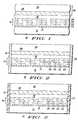
- FIGS. 1-3illustrate in cross-sectional views, the steps in fabricating a magnetic element with insulative veils according to the present invention.
- FIGS. 1-3illustrate in cross-sectional views a magnetic element according to the present invention. More particularly, illustrated in FIG. 1, is a first step in the fabrication of a patterned magnetic element 10 . Illustrated in FIG. 1, is a fully patterned magnetic element structure 10 . The structure includes a substrate 12 , a first electrode multilayer stack 14 , a spacer layer 16 including oxidized aluminum, and a second electrode multilayer stack 18 . It should be understood that spacer layer 16 is formed dependent upon the type of magnetic element being fabricated.
- spacer layer 16is formed of a dielectric material, and in a spin valve structure, spacer layer 16 is formed of a conductive material.
- First electrode multilayer stack 14 and second electrode multilayer stack 18include ferromagnetic layers.
- First electrode layers 14are formed on a base metal layer 13 , which is formed on substrate 12 .
- Base metal layer 13is disclosed as composed of a single metal material or layer or a stack of more than one metal material or layer.
- First electrode layer 14includes a first seed layer 20 , deposited on base metal layer 13 , a template layer 22 , a layer of antiferromagnetic pinning material 24 , and a fixed ferromagnetic layer 26 formed on and exchange coupled with the underlying antiferromagnetic pinning layer 24 .
- the pseudo spin-valve structurewould include a first electrode and a second electrode including a first switching field and a second switching field thereby defining the pseudo spin-valve structure.
- seed layer 20is formed of tantalum nitride (TaNx) having template layer 22 formed thereon.
- Template layer 22 in this particular embodimentis formed of ruthenium (Ru).
- Pinning layer 24is typically formed of iridium manganese (IrMn).
- ferromagnetic layer 26is described as fixed, or pinned, in that its magnetic moment is prevented from rotation in the presence of an applied magnetic field.
- Ferromagnetic layer 26is typically formed of alloys of one or more of the following: nickel (Ni), iron (Fe), and cobalt (Co).
- Second electrode stack 18includes a free ferromagnetic layer 28 and a protective contact layer 30 .
- the magnetic moment of the free ferromagnetic layer 28is not fixed, or pinned, by exchange coupling, and is free to rotate in the presence of an applied magnetic field.
- Free ferromagnetic layer 28is typically formed of a nickel iron (NiFe) alloy or a nickel iron cobalt (NiFeCo) alloy. It should be understood that a reversed, or flipped, structure is anticipated by this disclosure. More particularly, it is anticipated that the disclosed magnetic element can be formed to include a top fixed, or pinned layer, and thus described as a top pinned structure. In addition, a device including dual spacer layers is anticipated by this structure.
- magnetic element 10would structurally include a bottom pinned magnetic layer, a bottom spacer, or tunnel barrier layer, a free magnetic layer, a top spacer, or tunnel barrier layer, and a top pinned magnetic layer.
- the bottom pinned magnetic layer, the free magnetic layer and the top pinned magnetic layerinclude ferromagnetic layers.
- the bottom magnetic layeris optionally formed on a diffusion barrier layer which is formed on a metal lead which in turn is typically formed on some type of dielectric material.
- the diffusion barrier layeris typically formed of tantalum nitride (TaN), and aids in the thermal stability of the magnetic element.
- Fixed ferromagnetic layer 26is described as pinned, or fixed, in that its magnetic moment is prevented from rotation in the presence of an applied magnetic field.
- Ferromagnetic layer 26as previously stated is typically formed of alloys of one or more of the following: nickel (Ni), iron (Fe), and cobalt (Co).
- Magnetic layer 28is described as a free ferromagnetic layer. Accordingly, the magnetic moment of free ferromagnetic layer 28 is not fixed, or pinned, by exchange coupling, and is free to rotate in the presence of an applied magnetic field.
- Free ferromagnetic layer 28is formed co-linear with fixed magnetic layer 26 and of alloys of one or more of the following: nickel (Ni), iron (Fe), and cobalt (Co).
- Fixed ferromagnetic layer 26is described as having a thickness within a range of 5-500 ⁇ .
- Free ferromagnetic layer 28is described as having a thickness generally in the range of 5-500 ⁇ .
- spacer layer 16is formed of aluminum (Al) and oxygen (O). More particularly, spacer layer 16 is formed having a general formula of AlO x , where O ⁇ 1.5. It should be understood that when device 10 includes dual spacer layers, as previously discussed, that the second spacer layer would be formed of oxidized tantalum (Ta), generally having the formula TaO x , where O ⁇ 2.5.
- the next step in the method of fabricating device 10 according to the present inventionis etched to define device 10 having included as a part thereof conductive veils 32 .
- Conductive veils 32are formed subsequent to ion milling or reactive ion etching which is utilized to form device 10 .
- Conductive veils 32provide an electrical path between first electrode 14 and second electrode 18 and thereby cause device 10 to fail, due to the shorting out of the device across insulative spacer layer 16 .
- these veilsare etched off utilizing a wet etch process, which causes degraded device performance, and thus not suitable for MRAM device fabrication.
- wet etching away conductive veils 32is hard to utilize for deep submicron features, results in a non-uniform lateral over-etch, causing switching fields to vary, and results in an inability to make every cell the same shape and having the same switching field.
- conductive veils 32are next dry etched, using oxygen plasma ashing at either room temperature, more particularly at temperature of 150° C., or a higher temperature.
- This oxygen plasma etching of conductive veils 32provides for the transformation of conductive veils 32 into insulative veils 34 .
- Insulative veils 34are thus described as inactive having non-magnetic, dielectric properties.
- the fabrication of insulative veils 32results in a device having electrically isolated, first electrode 14 and second electrode 18 ;
- free magnetic layer 28can be formed anywhere in device 10 .
- Prior artdictates the fabrication of the free magnetic layer on the top of the device stack due to its fabrication as a thin layer, and the ability to turn portions of it into a dielectric material, thus electrically isolating the electrodes.
- This transformation of the thin free magnetic layer as disclosed and claimed hereinprovides for the blocking of the conduction path through the naturally formed conductive veil between the first electrode and the second electrode.
- free magnetic layer 28can be formed anywhere in the device stack.
- device 10may include a synthetic antiferromagnetic (SAF) structure that is formed between two tunnel barrier, or spacer, layers, or alternatively below a first spacer or tunnel barrier layer, or on a surface of a top spacer or tunnel barrier layer.
- SAFsynthetic antiferromagnetic
- a magnetic element with insulative veils and fabricating method thereofis disclosed in which the device structure and method of fabricating the device is improved based on the transformation of conductive veils to insulative veils.
- this techniquecan be applied to devices using patterned magnetic elements, such as magnetic sensors, magnetic recording heads, magnetic recording media, or the like. Accordingly, such instances are intended to be covered by this disclosure
Landscapes
- Engineering & Computer Science (AREA)
- Chemical & Material Sciences (AREA)
- Nanotechnology (AREA)
- Crystallography & Structural Chemistry (AREA)
- Power Engineering (AREA)
- Manufacturing & Machinery (AREA)
- Physics & Mathematics (AREA)
- General Physics & Mathematics (AREA)
- Spectroscopy & Molecular Physics (AREA)
- Condensed Matter Physics & Semiconductors (AREA)
- Computer Hardware Design (AREA)
- Hall/Mr Elements (AREA)
- Magnetic Heads (AREA)
- Soft Magnetic Materials (AREA)
- Thin Magnetic Films (AREA)
- Mram Or Spin Memory Techniques (AREA)
- Semiconductor Memories (AREA)
- Magnetic Treatment Devices (AREA)
- Treatment Of Fiber Materials (AREA)
Abstract
Description
- The present invention relates to magnetic elements for information storage and/or sensing and a fabricating method thereof, and more particularly, to a device and method of fabricating the magnetic element to include insulative veils.[0001]
- This application is related to a co-pending application that bears Motorola docket number CR97-133 and U.S. Ser. No. 09/144,686, entitled “MAGNETIC RANDOM ACCESS MEMORY AND FABRICATING METHOD THEREOF,” filed on Aug. 31, 1998, assigned to the same assignee and incorporated herein by this reference, co-pending application that bears Motorola docket number CR 97-158 and U.S. Ser. No. 08/986,764, entitled “PROCESS OF PATTERNING MAGNETIC FILMS” filed on Dec. 8, 1997, assigned to the same assignee and incorporated herein by this reference and issued U.S. Pat. No. 5,768,181, entitled “MAGNETIC DEVICE HAVING MULT-LAYER WITH INSULATING AND CONDUCTIVE LAYERS”, issued Jun. 16, 1998, assigned to the same assignee and incorporated herein by.[0002]
- Typically, a magnetic element, such as a magnetic memory element, has a structure that includes ferromagnetic layers separated by a non-magnetic layer. Information is stored as directions of magnetization vectors in magnetic layers. Magnetic vectors in one magnetic layer, for instance, are magnetically fixed or pinned, while the magnetization direction of the other magnetic layer is free to switch between the same and opposite directions that are called “parallel” and “anti-parallel” states, respectively. In response to parallel and anti-parallel states, the magnetic memory element represents two different resistances. The resistance has minimum and maximum values when the magnetization vectors of the two magnetic layers point in substantially the same and opposite directions, respectively. Accordingly, a detection of change in resistance allows a device, such as an MRAM device, to provide information stored in the magnetic memory element. The difference between the minimum and maximum resistance values, divided by the minimum resistance is known as the magnetoresistance ratio (MR).[0003]
- An MRAM device integrates magnetic elements, more particularly magnetic memory elements, and other circuits, for example, a control circuit for magnetic memory elements, comparators for detecting states in a magnetic memory element, input/output circuits, etc. These circuits are fabricated in the process of CMOS (complementary metal-oxide semiconductor) technology in order to lower the power consumption of the device.[0004]
- During typical magnetic element fabrication, such as MRAM element fabrication, metal films are grown by sputter deposition, evaporation, or epitaxy techniques. One such magnetic element structure includes a substrate, a base electrode multilayer stack, a synthetic antiferromagnetic (SAF) structure, an insulating tunnel barrier layer, and a top electrode stack. The base electrode layer stack is formed on the substrate and includes a first seed layer deposited on the substrate, a template layer formed on the seed layer, a layer of an antiferromagnetic material on the template layer and a pinned ferromagnetic layer formed on and exchange coupled with the underlying antiferromagnetic layer. The ferromagnetic layer is called the pinned layer because its magnetic moment (magnetization direction) is prevented from rotation in the presence of an applied magnetic field. The SAF structure includes a pinned ferromagnetic layer, and a fixed ferromagnetic layer, separated by a layer of ruthenium, or the like. The top electrode stack includes a free ferromagnetic layer and a protective layer formed on the free layer. The magnetic moment of the free ferromagnetic layer is not pinned by exchange coupling, and is thus free to rotate in the presence of applied magnetic fields.[0005]
- During fabrication of these magnetic elements, ion milling is commonly used for the dry etching of the magnetic materials. However, during the process of dry etching, conducting veils are left remaining on the sides of the magnetic tunnel junction (MTJ). These remaining veils lead to electrical shorting of the device between the bottom and top electrodes, more particularly across the insulating tunnel barrier. Currently, wet etching techniques are used in the semiconductor industry to etch away the veils, but are not amenable for use in conjunction with magnetic materials due to their chemical attack on the magnetic materials leading to device performance degradation.[0006]
- To avoid the shorting problem caused by veils, the current etching process is done in two steps. First the top magnetic layer of the magnetic element is etched or defined, then the whole stack is etched using a dry etch technique; or vice versa. Veils may be minimized by varying the etching beam angle relative to the wafer surface. Since the edges of the top and bottom magnetic layers do not overlap, the veils do not cause a shorting problem between the top and bottom magnetic layers. However, this is a very complex etching process. Stopping the etch of the top magnetic layer without over-etching through the ultra thin tunnel barrier, and into the bottom magnetic layer is very difficult to do. Over-etching into the bottom magnetic layer will cause unwanted magnetic poles shifting the resistance-magnetic field response of the magnetic element. This technique also limits the free magnetic layer to be placed on top of the tunnel barrier.[0007]
- Accordingly, it is a purpose of the present invention to provide for a magnetic element having formed as a part thereof, insulating veils, which no longer include conductive or magnetic properties.[0008]
- It is a still further purpose of the present invention to provide a method of forming a magnetic element with insulating veils.[0009]
- It is another purpose of the present invention to provide a method of fabricating a magnetic element that includes plasma oxygen ashing of the magnetic stack to transform conducting veils into insulating veils.[0010]
- It is another purpose of the present invention to provide a method of forming a magnetic element with insulating veils which is amenable to simple and high throughput manufacturing.[0011]
- It is still a further purpose of the present invention to provide a method of forming a magnetic element with insulating veils that allows for the formation of the free magnetic layer anywhere within the magnetic element stack.[0012]
- These needs and others are substantially met through provision of a magnetic element including a base metal layer, a first electrode, a second electrode and a spacer layer. The base metal layer is positioned on an uppermost surface of a substrate element. A spacer layer is located between the ferromagnetic layers for permitting tunneling current in a direction generally perpendicular to the ferromagnetic layers. In an alternative embodiment, the structure is described as including a SAF structure to allow for proper balancing of magnetostatic interaction in the magnetic element. The device includes insulative veils characterized as electrically isolating the first electrode and the second electrode, the insulative veils including non-magnetic and insulating dielectric properties. Additionally disclosed is a method of fabricating the magnetic element with insulative veils that have been transformed from having conductive properties to having insulative properties through oxygen plasma ashing techniques.[0013]
- FIGS. 1-3 illustrate in cross-sectional views, the steps in fabricating a magnetic element with insulative veils according to the present invention.[0014]
- During the course of this description, like numbers are used to identify like elements according to the different figures that illustrate the invention. FIGS. 1-3 illustrate in cross-sectional views a magnetic element according to the present invention. More particularly, illustrated in FIG. 1, is a first step in the fabrication of a patterned[0015]
magnetic element 10. Illustrated in FIG. 1, is a fully patternedmagnetic element structure 10. The structure includes asubstrate 12, a firstelectrode multilayer stack 14, aspacer layer 16 including oxidized aluminum, and a secondelectrode multilayer stack 18. It should be understood thatspacer layer 16 is formed dependent upon the type of magnetic element being fabricated. More particularly, in a MTJ structure,spacer layer 16 is formed of a dielectric material, and in a spin valve structure,spacer layer 16 is formed of a conductive material. Firstelectrode multilayer stack 14 and secondelectrode multilayer stack 18 include ferromagnetic layers.First electrode layers 14 are formed on abase metal layer 13, which is formed onsubstrate 12.Base metal layer 13 is disclosed as composed of a single metal material or layer or a stack of more than one metal material or layer.First electrode layer 14 includes afirst seed layer 20, deposited onbase metal layer 13, atemplate layer 22, a layer ofantiferromagnetic pinning material 24, and a fixedferromagnetic layer 26 formed on and exchange coupled with the underlyingantiferromagnetic pinning layer 24. It should be understood that anticipated by this disclosure is a pseudo spin-valve structure that would not include the antiferromagnetic pinning layer. In this instance, the pseudo spin-valve structure would include a first electrode and a second electrode including a first switching field and a second switching field thereby defining the pseudo spin-valve structure. - Typically,[0016]
seed layer 20 is formed of tantalum nitride (TaNx) havingtemplate layer 22 formed thereon.Template layer 22 in this particular embodiment is formed of ruthenium (Ru). Pinninglayer 24 is typically formed of iridium manganese (IrMn). - In this particular embodiment,[0017]
ferromagnetic layer 26 is described as fixed, or pinned, in that its magnetic moment is prevented from rotation in the presence of an applied magnetic field.Ferromagnetic layer 26 is typically formed of alloys of one or more of the following: nickel (Ni), iron (Fe), and cobalt (Co). - [0018]
Second electrode stack 18 includes a freeferromagnetic layer 28 and aprotective contact layer 30. The magnetic moment of the freeferromagnetic layer 28 is not fixed, or pinned, by exchange coupling, and is free to rotate in the presence of an applied magnetic field. Freeferromagnetic layer 28 is typically formed of a nickel iron (NiFe) alloy or a nickel iron cobalt (NiFeCo) alloy. It should be understood that a reversed, or flipped, structure is anticipated by this disclosure. More particularly, it is anticipated that the disclosed magnetic element can be formed to include a top fixed, or pinned layer, and thus described as a top pinned structure. In addition, a device including dual spacer layers is anticipated by this structure. In this instance,magnetic element 10 would structurally include a bottom pinned magnetic layer, a bottom spacer, or tunnel barrier layer, a free magnetic layer, a top spacer, or tunnel barrier layer, and a top pinned magnetic layer. The bottom pinned magnetic layer, the free magnetic layer and the top pinned magnetic layer include ferromagnetic layers. The bottom magnetic layer is optionally formed on a diffusion barrier layer which is formed on a metal lead which in turn is typically formed on some type of dielectric material. The diffusion barrier layer is typically formed of tantalum nitride (TaN), and aids in the thermal stability of the magnetic element. - Fixed[0019]
ferromagnetic layer 26 is described as pinned, or fixed, in that its magnetic moment is prevented from rotation in the presence of an applied magnetic field.Ferromagnetic layer 26 as previously stated is typically formed of alloys of one or more of the following: nickel (Ni), iron (Fe), and cobalt (Co).Magnetic layer 28 is described as a free ferromagnetic layer. Accordingly, the magnetic moment of freeferromagnetic layer 28 is not fixed, or pinned, by exchange coupling, and is free to rotate in the presence of an applied magnetic field. Freeferromagnetic layer 28 is formed co-linear with fixedmagnetic layer 26 and of alloys of one or more of the following: nickel (Ni), iron (Fe), and cobalt (Co). Fixedferromagnetic layer 26 is described as having a thickness within a range of 5-500 Å. Freeferromagnetic layer 28 is described as having a thickness generally in the range of 5-500Å. - In this particular embodiment,[0020]
spacer layer 16 is formed of aluminum (Al) and oxygen (O). More particularly,spacer layer 16 is formed having a general formula of AlOx, where O<×≦1.5. It should be understood that whendevice 10 includes dual spacer layers, as previously discussed, that the second spacer layer would be formed of oxidized tantalum (Ta), generally having the formula TaOx, where O<×≦2.5. - Illustrated in FIG. 2, the next step in the method of fabricating[0021]
device 10 according to the present invention. More particularly, as illustrated, the plurality of epitaxially deposited layers are etched to definedevice 10 having included as a part thereofconductive veils 32.Conductive veils 32 are formed subsequent to ion milling or reactive ion etching which is utilized to formdevice 10.Conductive veils 32 provide an electrical path betweenfirst electrode 14 andsecond electrode 18 and thereby causedevice 10 to fail, due to the shorting out of the device acrossinsulative spacer layer 16. Typically these veils are etched off utilizing a wet etch process, which causes degraded device performance, and thus not suitable for MRAM device fabrication. In addition, wet etching awayconductive veils 32 is hard to utilize for deep submicron features, results in a non-uniform lateral over-etch, causing switching fields to vary, and results in an inability to make every cell the same shape and having the same switching field. - Referring now to FIG. 3, illustrated is the next step in the method of fabricating[0022]
device 10 according to the present invention. More particularly, as illustrated,conductive veils 32 are next dry etched, using oxygen plasma ashing at either room temperature, more particularly at temperature of 150° C., or a higher temperature. This oxygen plasma etching ofconductive veils 32 provides for the transformation ofconductive veils 32 intoinsulative veils 34.Insulative veils 34 are thus described as inactive having non-magnetic, dielectric properties. The fabrication ofinsulative veils 32 results in a device having electrically isolated,first electrode 14 andsecond electrode 18; - It should be understood that due to the ability to electrically isolate[0023]
first electrode 14 andsecond electrode 18, that freemagnetic layer 28 can be formed anywhere indevice 10. Prior art dictates the fabrication of the free magnetic layer on the top of the device stack due to its fabrication as a thin layer, and the ability to turn portions of it into a dielectric material, thus electrically isolating the electrodes. This transformation of the thin free magnetic layer as disclosed and claimed herein provides for the blocking of the conduction path through the naturally formed conductive veil between the first electrode and the second electrode. In this particular invention, in that the conductive veils have been transformed intoinsulative veils 34, freemagnetic layer 28 can be formed anywhere in the device stack. It should be understood that it is anticipated by this disclosure thatdevice 10 may include a synthetic antiferromagnetic (SAF) structure that is formed between two tunnel barrier, or spacer, layers, or alternatively below a first spacer or tunnel barrier layer, or on a surface of a top spacer or tunnel barrier layer. - Thus, a magnetic element with insulative veils and fabricating method thereof is disclosed in which the device structure and method of fabricating the device is improved based on the transformation of conductive veils to insulative veils. As disclosed, this technique can be applied to devices using patterned magnetic elements, such as magnetic sensors, magnetic recording heads, magnetic recording media, or the like. Accordingly, such instances are intended to be covered by this disclosure[0024]
Claims (8)
Priority Applications (1)
| Application Number | Priority Date | Filing Date | Title |
|---|---|---|---|
| US10/830,264US6912107B2 (en) | 2000-04-28 | 2004-04-21 | Magnetic element with insulating veils and fabricating method thereof |
Applications Claiming Priority (3)
| Application Number | Priority Date | Filing Date | Title |
|---|---|---|---|
| US56073800A | 2000-04-28 | 2000-04-28 | |
| US10/349,702US6835423B2 (en) | 2000-04-28 | 2003-01-22 | Method of fabricating a magnetic element with insulating veils |
| US10/830,264US6912107B2 (en) | 2000-04-28 | 2004-04-21 | Magnetic element with insulating veils and fabricating method thereof |
Related Parent Applications (1)
| Application Number | Title | Priority Date | Filing Date |
|---|---|---|---|
| US10/349,702DivisionUS6835423B2 (en) | 2000-04-28 | 2003-01-22 | Method of fabricating a magnetic element with insulating veils |
Publications (2)
| Publication Number | Publication Date |
|---|---|
| US20040197579A1true US20040197579A1 (en) | 2004-10-07 |
| US6912107B2 US6912107B2 (en) | 2005-06-28 |
Family
ID=24239151
Family Applications (2)
| Application Number | Title | Priority Date | Filing Date |
|---|---|---|---|
| US10/349,702Expired - LifetimeUS6835423B2 (en) | 2000-04-28 | 2003-01-22 | Method of fabricating a magnetic element with insulating veils |
| US10/830,264Expired - Fee RelatedUS6912107B2 (en) | 2000-04-28 | 2004-04-21 | Magnetic element with insulating veils and fabricating method thereof |
Family Applications Before (1)
| Application Number | Title | Priority Date | Filing Date |
|---|---|---|---|
| US10/349,702Expired - LifetimeUS6835423B2 (en) | 2000-04-28 | 2003-01-22 | Method of fabricating a magnetic element with insulating veils |
Country Status (9)
| Country | Link |
|---|---|
| US (2) | US6835423B2 (en) |
| EP (1) | EP1279176B1 (en) |
| JP (1) | JP2003534647A (en) |
| KR (1) | KR20030014209A (en) |
| AT (1) | ATE363719T1 (en) |
| AU (1) | AU2001255555A1 (en) |
| DE (1) | DE60128678T2 (en) |
| TW (1) | TW504713B (en) |
| WO (1) | WO2001084570A2 (en) |
Cited By (15)
| Publication number | Priority date | Publication date | Assignee | Title |
|---|---|---|---|---|
| US20100090300A1 (en)* | 2008-10-09 | 2010-04-15 | Seagate Technology Llc | Mram cells including coupled free ferromagnetic layers for stabilization |
| US7985994B2 (en) | 2008-09-29 | 2011-07-26 | Seagate Technology Llc | Flux-closed STRAM with electronically reflective insulative spacer |
| US20110194335A1 (en)* | 2008-10-09 | 2011-08-11 | Seagate Technology Llc | Magnetic memory with phonon glass electron crystal material |
| US7999338B2 (en) | 2009-07-13 | 2011-08-16 | Seagate Technology Llc | Magnetic stack having reference layers with orthogonal magnetization orientation directions |
| US8039913B2 (en) | 2008-10-09 | 2011-10-18 | Seagate Technology Llc | Magnetic stack with laminated layer |
| US8045366B2 (en) | 2008-11-05 | 2011-10-25 | Seagate Technology Llc | STRAM with composite free magnetic element |
| US8043732B2 (en) | 2008-11-11 | 2011-10-25 | Seagate Technology Llc | Memory cell with radial barrier |
| US8169810B2 (en) | 2008-10-08 | 2012-05-01 | Seagate Technology Llc | Magnetic memory with asymmetric energy barrier |
| US8179716B2 (en) | 2008-05-23 | 2012-05-15 | Seagate Technology Llc | Non-volatile programmable logic gates and adders |
| US8203871B2 (en) | 2008-05-23 | 2012-06-19 | Seagate Technology Llc | Reconfigurable magnetic logic device using spin torque |
| US8203874B2 (en) | 2009-01-29 | 2012-06-19 | Seagate Technology Llc | Staggered magnetic tunnel junction |
| US8289756B2 (en) | 2008-11-25 | 2012-10-16 | Seagate Technology Llc | Non volatile memory including stabilizing structures |
| US8400823B2 (en) | 2008-08-26 | 2013-03-19 | Seagate Technology Llc | Memory with separate read and write paths |
| US8456903B2 (en) | 2008-11-12 | 2013-06-04 | Seagate Technology Llc | Magnetic memory with porous non-conductive current confinement layer |
| US8659852B2 (en) | 2008-04-21 | 2014-02-25 | Seagate Technology Llc | Write-once magentic junction memory array |
Families Citing this family (88)
| Publication number | Priority date | Publication date | Assignee | Title |
|---|---|---|---|---|
| JP4729109B2 (en)* | 2000-09-11 | 2011-07-20 | 株式会社東芝 | Ferromagnetic tunnel junction device and manufacturing method thereof |
| US7394626B2 (en)* | 2002-11-01 | 2008-07-01 | Nec Corporation | Magnetoresistance device with a diffusion barrier between a conductor and a magnetoresistance element and method of fabricating the same |
| JP2004200245A (en)* | 2002-12-16 | 2004-07-15 | Nec Corp | Magnetoresistive element and manufacturing method therefor |
| US8755222B2 (en) | 2003-08-19 | 2014-06-17 | New York University | Bipolar spin-transfer switching |
| US7573737B2 (en)* | 2003-08-19 | 2009-08-11 | New York University | High speed low power magnetic devices based on current induced spin-momentum transfer |
| US7911832B2 (en) | 2003-08-19 | 2011-03-22 | New York University | High speed low power magnetic devices based on current induced spin-momentum transfer |
| US7602000B2 (en)* | 2003-11-19 | 2009-10-13 | International Business Machines Corporation | Spin-current switched magnetic memory element suitable for circuit integration and method of fabricating the memory element |
| US6974708B2 (en)* | 2004-04-08 | 2005-12-13 | Headway Technologies, Inc. | Oxidation structure/method to fabricate a high-performance magnetic tunneling junction MRAM |
| US7265404B2 (en)* | 2005-08-30 | 2007-09-04 | Magic Technologies, Inc. | Bottom conductor for integrated MRAM |
| US9812184B2 (en) | 2007-10-31 | 2017-11-07 | New York University | Current induced spin-momentum transfer stack with dual insulating layers |
| JP5514256B2 (en)* | 2012-05-18 | 2014-06-04 | 株式会社東芝 | Magnetic memory element and manufacturing method thereof |
| US9082888B2 (en) | 2012-10-17 | 2015-07-14 | New York University | Inverted orthogonal spin transfer layer stack |
| US9082950B2 (en) | 2012-10-17 | 2015-07-14 | New York University | Increased magnetoresistance in an inverted orthogonal spin transfer layer stack |
| US8982613B2 (en) | 2013-06-17 | 2015-03-17 | New York University | Scalable orthogonal spin transfer magnetic random access memory devices with reduced write error rates |
| US9263667B1 (en) | 2014-07-25 | 2016-02-16 | Spin Transfer Technologies, Inc. | Method for manufacturing MTJ memory device |
| US9337412B2 (en) | 2014-09-22 | 2016-05-10 | Spin Transfer Technologies, Inc. | Magnetic tunnel junction structure for MRAM device |
| US9728712B2 (en) | 2015-04-21 | 2017-08-08 | Spin Transfer Technologies, Inc. | Spin transfer torque structure for MRAM devices having a spin current injection capping layer |
| US10468590B2 (en) | 2015-04-21 | 2019-11-05 | Spin Memory, Inc. | High annealing temperature perpendicular magnetic anisotropy structure for magnetic random access memory |
| US9853206B2 (en) | 2015-06-16 | 2017-12-26 | Spin Transfer Technologies, Inc. | Precessional spin current structure for MRAM |
| US9773974B2 (en) | 2015-07-30 | 2017-09-26 | Spin Transfer Technologies, Inc. | Polishing stop layer(s) for processing arrays of semiconductor elements |
| US10163479B2 (en) | 2015-08-14 | 2018-12-25 | Spin Transfer Technologies, Inc. | Method and apparatus for bipolar memory write-verify |
| US9741926B1 (en) | 2016-01-28 | 2017-08-22 | Spin Transfer Technologies, Inc. | Memory cell having magnetic tunnel junction and thermal stability enhancement layer |
| US10991410B2 (en) | 2016-09-27 | 2021-04-27 | Spin Memory, Inc. | Bi-polar write scheme |
| US11119936B2 (en) | 2016-09-27 | 2021-09-14 | Spin Memory, Inc. | Error cache system with coarse and fine segments for power optimization |
| US10628316B2 (en) | 2016-09-27 | 2020-04-21 | Spin Memory, Inc. | Memory device with a plurality of memory banks where each memory bank is associated with a corresponding memory instruction pipeline and a dynamic redundancy register |
| US10437723B2 (en) | 2016-09-27 | 2019-10-08 | Spin Memory, Inc. | Method of flushing the contents of a dynamic redundancy register to a secure storage area during a power down in a memory device |
| US10366774B2 (en) | 2016-09-27 | 2019-07-30 | Spin Memory, Inc. | Device with dynamic redundancy registers |
| US10818331B2 (en) | 2016-09-27 | 2020-10-27 | Spin Memory, Inc. | Multi-chip module for MRAM devices with levels of dynamic redundancy registers |
| US10437491B2 (en) | 2016-09-27 | 2019-10-08 | Spin Memory, Inc. | Method of processing incomplete memory operations in a memory device during a power up sequence and a power down sequence using a dynamic redundancy register |
| US11119910B2 (en) | 2016-09-27 | 2021-09-14 | Spin Memory, Inc. | Heuristics for selecting subsegments for entry in and entry out operations in an error cache system with coarse and fine grain segments |
| US10446210B2 (en) | 2016-09-27 | 2019-10-15 | Spin Memory, Inc. | Memory instruction pipeline with a pre-read stage for a write operation for reducing power consumption in a memory device that uses dynamic redundancy registers |
| US10546625B2 (en) | 2016-09-27 | 2020-01-28 | Spin Memory, Inc. | Method of optimizing write voltage based on error buffer occupancy |
| US10360964B2 (en) | 2016-09-27 | 2019-07-23 | Spin Memory, Inc. | Method of writing contents in memory during a power up sequence using a dynamic redundancy register in a memory device |
| US10460781B2 (en) | 2016-09-27 | 2019-10-29 | Spin Memory, Inc. | Memory device with a dual Y-multiplexer structure for performing two simultaneous operations on the same row of a memory bank |
| US11151042B2 (en) | 2016-09-27 | 2021-10-19 | Integrated Silicon Solution, (Cayman) Inc. | Error cache segmentation for power reduction |
| US10665777B2 (en) | 2017-02-28 | 2020-05-26 | Spin Memory, Inc. | Precessional spin current structure with non-magnetic insertion layer for MRAM |
| US10672976B2 (en) | 2017-02-28 | 2020-06-02 | Spin Memory, Inc. | Precessional spin current structure with high in-plane magnetization for MRAM |
| US10032978B1 (en) | 2017-06-27 | 2018-07-24 | Spin Transfer Technologies, Inc. | MRAM with reduced stray magnetic fields |
| US10489245B2 (en) | 2017-10-24 | 2019-11-26 | Spin Memory, Inc. | Forcing stuck bits, waterfall bits, shunt bits and low TMR bits to short during testing and using on-the-fly bit failure detection and bit redundancy remapping techniques to correct them |
| US10529439B2 (en) | 2017-10-24 | 2020-01-07 | Spin Memory, Inc. | On-the-fly bit failure detection and bit redundancy remapping techniques to correct for fixed bit defects |
| US10481976B2 (en) | 2017-10-24 | 2019-11-19 | Spin Memory, Inc. | Forcing bits as bad to widen the window between the distributions of acceptable high and low resistive bits thereby lowering the margin and increasing the speed of the sense amplifiers |
| US10656994B2 (en) | 2017-10-24 | 2020-05-19 | Spin Memory, Inc. | Over-voltage write operation of tunnel magnet-resistance (“TMR”) memory device and correcting failure bits therefrom by using on-the-fly bit failure detection and bit redundancy remapping techniques |
| US10679685B2 (en) | 2017-12-27 | 2020-06-09 | Spin Memory, Inc. | Shared bit line array architecture for magnetoresistive memory |
| US10424726B2 (en) | 2017-12-28 | 2019-09-24 | Spin Memory, Inc. | Process for improving photoresist pillar adhesion during MRAM fabrication |
| US10395712B2 (en) | 2017-12-28 | 2019-08-27 | Spin Memory, Inc. | Memory array with horizontal source line and sacrificial bitline per virtual source |
| US10395711B2 (en) | 2017-12-28 | 2019-08-27 | Spin Memory, Inc. | Perpendicular source and bit lines for an MRAM array |
| US10360962B1 (en) | 2017-12-28 | 2019-07-23 | Spin Memory, Inc. | Memory array with individually trimmable sense amplifiers |
| US10811594B2 (en) | 2017-12-28 | 2020-10-20 | Spin Memory, Inc. | Process for hard mask development for MRAM pillar formation using photolithography |
| US10891997B2 (en) | 2017-12-28 | 2021-01-12 | Spin Memory, Inc. | Memory array with horizontal source line and a virtual source line |
| US10516094B2 (en) | 2017-12-28 | 2019-12-24 | Spin Memory, Inc. | Process for creating dense pillars using multiple exposures for MRAM fabrication |
| US10840439B2 (en) | 2017-12-29 | 2020-11-17 | Spin Memory, Inc. | Magnetic tunnel junction (MTJ) fabrication methods and systems |
| US10236047B1 (en) | 2017-12-29 | 2019-03-19 | Spin Memory, Inc. | Shared oscillator (STNO) for MRAM array write-assist in orthogonal STT-MRAM |
| US10236048B1 (en) | 2017-12-29 | 2019-03-19 | Spin Memory, Inc. | AC current write-assist in orthogonal STT-MRAM |
| US10784439B2 (en) | 2017-12-29 | 2020-09-22 | Spin Memory, Inc. | Precessional spin current magnetic tunnel junction devices and methods of manufacture |
| US10546624B2 (en) | 2017-12-29 | 2020-01-28 | Spin Memory, Inc. | Multi-port random access memory |
| US10199083B1 (en) | 2017-12-29 | 2019-02-05 | Spin Transfer Technologies, Inc. | Three-terminal MRAM with ac write-assist for low read disturb |
| US10270027B1 (en) | 2017-12-29 | 2019-04-23 | Spin Memory, Inc. | Self-generating AC current assist in orthogonal STT-MRAM |
| US10886330B2 (en) | 2017-12-29 | 2021-01-05 | Spin Memory, Inc. | Memory device having overlapping magnetic tunnel junctions in compliance with a reference pitch |
| US10424723B2 (en) | 2017-12-29 | 2019-09-24 | Spin Memory, Inc. | Magnetic tunnel junction devices including an optimization layer |
| US10367139B2 (en) | 2017-12-29 | 2019-07-30 | Spin Memory, Inc. | Methods of manufacturing magnetic tunnel junction devices |
| US10840436B2 (en) | 2017-12-29 | 2020-11-17 | Spin Memory, Inc. | Perpendicular magnetic anisotropy interface tunnel junction devices and methods of manufacture |
| US10360961B1 (en) | 2017-12-29 | 2019-07-23 | Spin Memory, Inc. | AC current pre-charge write-assist in orthogonal STT-MRAM |
| US10236439B1 (en) | 2017-12-30 | 2019-03-19 | Spin Memory, Inc. | Switching and stability control for perpendicular magnetic tunnel junction device |
| US10141499B1 (en) | 2017-12-30 | 2018-11-27 | Spin Transfer Technologies, Inc. | Perpendicular magnetic tunnel junction device with offset precessional spin current layer |
| US10255962B1 (en) | 2017-12-30 | 2019-04-09 | Spin Memory, Inc. | Microwave write-assist in orthogonal STT-MRAM |
| US10319900B1 (en) | 2017-12-30 | 2019-06-11 | Spin Memory, Inc. | Perpendicular magnetic tunnel junction device with precessional spin current layer having a modulated moment density |
| US10229724B1 (en) | 2017-12-30 | 2019-03-12 | Spin Memory, Inc. | Microwave write-assist in series-interconnected orthogonal STT-MRAM devices |
| US10339993B1 (en) | 2017-12-30 | 2019-07-02 | Spin Memory, Inc. | Perpendicular magnetic tunnel junction device with skyrmionic assist layers for free layer switching |
| US10468588B2 (en) | 2018-01-05 | 2019-11-05 | Spin Memory, Inc. | Perpendicular magnetic tunnel junction device with skyrmionic enhancement layers for the precessional spin current magnetic layer |
| US10438995B2 (en) | 2018-01-08 | 2019-10-08 | Spin Memory, Inc. | Devices including magnetic tunnel junctions integrated with selectors |
| US10438996B2 (en) | 2018-01-08 | 2019-10-08 | Spin Memory, Inc. | Methods of fabricating magnetic tunnel junctions integrated with selectors |
| US10446744B2 (en) | 2018-03-08 | 2019-10-15 | Spin Memory, Inc. | Magnetic tunnel junction wafer adaptor used in magnetic annealing furnace and method of using the same |
| US10388861B1 (en) | 2018-03-08 | 2019-08-20 | Spin Memory, Inc. | Magnetic tunnel junction wafer adaptor used in magnetic annealing furnace and method of using the same |
| US11107978B2 (en) | 2018-03-23 | 2021-08-31 | Spin Memory, Inc. | Methods of manufacturing three-dimensional arrays with MTJ devices including a free magnetic trench layer and a planar reference magnetic layer |
| US10784437B2 (en) | 2018-03-23 | 2020-09-22 | Spin Memory, Inc. | Three-dimensional arrays with MTJ devices including a free magnetic trench layer and a planar reference magnetic layer |
| US11107974B2 (en) | 2018-03-23 | 2021-08-31 | Spin Memory, Inc. | Magnetic tunnel junction devices including a free magnetic trench layer and a planar reference magnetic layer |
| US20190296220A1 (en) | 2018-03-23 | 2019-09-26 | Spin Transfer Technologies, Inc. | Magnetic Tunnel Junction Devices Including an Annular Free Magnetic Layer and a Planar Reference Magnetic Layer |
| US10411185B1 (en) | 2018-05-30 | 2019-09-10 | Spin Memory, Inc. | Process for creating a high density magnetic tunnel junction array test platform |
| US10593396B2 (en) | 2018-07-06 | 2020-03-17 | Spin Memory, Inc. | Multi-bit cell read-out techniques for MRAM cells with mixed pinned magnetization orientations |
| US10559338B2 (en) | 2018-07-06 | 2020-02-11 | Spin Memory, Inc. | Multi-bit cell read-out techniques |
| US10600478B2 (en) | 2018-07-06 | 2020-03-24 | Spin Memory, Inc. | Multi-bit cell read-out techniques for MRAM cells with mixed pinned magnetization orientations |
| US10692569B2 (en) | 2018-07-06 | 2020-06-23 | Spin Memory, Inc. | Read-out techniques for multi-bit cells |
| US10650875B2 (en) | 2018-08-21 | 2020-05-12 | Spin Memory, Inc. | System for a wide temperature range nonvolatile memory |
| US10699761B2 (en) | 2018-09-18 | 2020-06-30 | Spin Memory, Inc. | Word line decoder memory architecture |
| US11621293B2 (en) | 2018-10-01 | 2023-04-04 | Integrated Silicon Solution, (Cayman) Inc. | Multi terminal device stack systems and methods |
| US10971680B2 (en) | 2018-10-01 | 2021-04-06 | Spin Memory, Inc. | Multi terminal device stack formation methods |
| US10580827B1 (en) | 2018-11-16 | 2020-03-03 | Spin Memory, Inc. | Adjustable stabilizer/polarizer method for MRAM with enhanced stability and efficient switching |
| US11107979B2 (en) | 2018-12-28 | 2021-08-31 | Spin Memory, Inc. | Patterned silicide structures and methods of manufacture |
Citations (3)
| Publication number | Priority date | Publication date | Assignee | Title |
|---|---|---|---|---|
| US6165803A (en)* | 1999-05-17 | 2000-12-26 | Motorola, Inc. | Magnetic random access memory and fabricating method thereof |
| US6238582B1 (en)* | 1999-03-30 | 2001-05-29 | Veeco Instruments, Inc. | Reactive ion beam etching method and a thin film head fabricated using the method |
| US6277762B1 (en)* | 1997-03-13 | 2001-08-21 | Applied Materials, Inc. | Method for removing redeposited veils from etched platinum |
Family Cites Families (15)
| Publication number | Priority date | Publication date | Assignee | Title |
|---|---|---|---|---|
| US5284701A (en)* | 1991-02-11 | 1994-02-08 | Ashland Oil, Inc. | Carbon fiber reinforced coatings |
| KR0172408B1 (en) | 1995-12-11 | 1999-03-30 | 김광호 | Non-volatile semiconductor memory and method driving the same |
| US5764567A (en) | 1996-11-27 | 1998-06-09 | International Business Machines Corporation | Magnetic tunnel junction device with nonferromagnetic interface layer for improved magnetic field response |
| US5650958A (en) | 1996-03-18 | 1997-07-22 | International Business Machines Corporation | Magnetic tunnel junctions with controlled magnetic response |
| JPH10270776A (en)* | 1997-03-25 | 1998-10-09 | Sanyo Electric Co Ltd | Method for manufacturing magnetoresistance effect film |
| US6008129A (en) | 1997-08-28 | 1999-12-28 | Motorola, Inc. | Process for forming a semiconductor device |
| US5966012A (en) | 1997-10-07 | 1999-10-12 | International Business Machines Corporation | Magnetic tunnel junction device with improved fixed and free ferromagnetic layers |
| US6005753A (en) | 1998-05-29 | 1999-12-21 | International Business Machines Corporation | Magnetic tunnel junction magnetoresistive read head with longitudinal and transverse bias |
| US6114719A (en) | 1998-05-29 | 2000-09-05 | International Business Machines Corporation | Magnetic tunnel junction memory cell with in-stack biasing of the free ferromagnetic layer and memory array using the cell |
| JP3606738B2 (en) | 1998-06-05 | 2005-01-05 | 東京応化工業株式会社 | Treatment liquid after ashing and treatment method using the same |
| US6330136B1 (en)* | 1998-10-14 | 2001-12-11 | Read-Rite Corporation | Magnetic read sensor with SDT tri-layer and method for making same |
| US6242350B1 (en) | 1999-03-18 | 2001-06-05 | Taiwan Semiconductor Manufacturing Company | Post gate etch cleaning process for self-aligned gate mosfets |
| JP3446720B2 (en)* | 1999-05-31 | 2003-09-16 | 日本電気株式会社 | Magnetoresistive element, method of manufacturing the same, and magnetic recording apparatus using the same |
| JP2001196659A (en)* | 2000-01-12 | 2001-07-19 | Tdk Corp | Tunnel magnetoresistive effect element, thin magnetic film head, memory element, and manufacturing method for them |
| US6281538B1 (en) | 2000-03-22 | 2001-08-28 | Motorola, Inc. | Multi-layer tunneling device with a graded stoichiometry insulating layer |
- 2001
- 2001-04-13TWTW090108916Apatent/TW504713B/ennot_activeIP Right Cessation
- 2001-04-20DEDE60128678Tpatent/DE60128678T2/ennot_activeExpired - Fee Related
- 2001-04-20EPEP01928727Apatent/EP1279176B1/ennot_activeExpired - Lifetime
- 2001-04-20JPJP2001581295Apatent/JP2003534647A/enactivePending
- 2001-04-20WOPCT/US2001/012953patent/WO2001084570A2/enactiveIP Right Grant
- 2001-04-20KRKR1020027014490Apatent/KR20030014209A/ennot_activeCeased
- 2001-04-20AUAU2001255555Apatent/AU2001255555A1/ennot_activeAbandoned
- 2001-04-20ATAT01928727Tpatent/ATE363719T1/ennot_activeIP Right Cessation
- 2003
- 2003-01-22USUS10/349,702patent/US6835423B2/ennot_activeExpired - Lifetime
- 2004
- 2004-04-21USUS10/830,264patent/US6912107B2/ennot_activeExpired - Fee Related
Patent Citations (3)
| Publication number | Priority date | Publication date | Assignee | Title |
|---|---|---|---|---|
| US6277762B1 (en)* | 1997-03-13 | 2001-08-21 | Applied Materials, Inc. | Method for removing redeposited veils from etched platinum |
| US6238582B1 (en)* | 1999-03-30 | 2001-05-29 | Veeco Instruments, Inc. | Reactive ion beam etching method and a thin film head fabricated using the method |
| US6165803A (en)* | 1999-05-17 | 2000-12-26 | Motorola, Inc. | Magnetic random access memory and fabricating method thereof |
Cited By (32)
| Publication number | Priority date | Publication date | Assignee | Title |
|---|---|---|---|---|
| US8659852B2 (en) | 2008-04-21 | 2014-02-25 | Seagate Technology Llc | Write-once magentic junction memory array |
| US8179716B2 (en) | 2008-05-23 | 2012-05-15 | Seagate Technology Llc | Non-volatile programmable logic gates and adders |
| US8203871B2 (en) | 2008-05-23 | 2012-06-19 | Seagate Technology Llc | Reconfigurable magnetic logic device using spin torque |
| US8422278B2 (en) | 2008-08-26 | 2013-04-16 | Seagate Technology Llc | Memory with separate read and write paths |
| US8400823B2 (en) | 2008-08-26 | 2013-03-19 | Seagate Technology Llc | Memory with separate read and write paths |
| US8711608B2 (en) | 2008-08-26 | 2014-04-29 | Seagate Technology Llc | Memory with separate read and write paths |
| US7985994B2 (en) | 2008-09-29 | 2011-07-26 | Seagate Technology Llc | Flux-closed STRAM with electronically reflective insulative spacer |
| US9041083B2 (en) | 2008-09-29 | 2015-05-26 | Seagate Technology Llc | Flux-closed STRAM with electronically reflective insulative spacer |
| US8362534B2 (en) | 2008-09-29 | 2013-01-29 | Seagate Technology Llc | Flux-closed STRAM with electronically reflective insulative spacer |
| US8169810B2 (en) | 2008-10-08 | 2012-05-01 | Seagate Technology Llc | Magnetic memory with asymmetric energy barrier |
| US8634223B2 (en) | 2008-10-08 | 2014-01-21 | Seagate Technology Llc | Magnetic memory with asymmetric energy barrier |
| US8039913B2 (en) | 2008-10-09 | 2011-10-18 | Seagate Technology Llc | Magnetic stack with laminated layer |
| US20100090300A1 (en)* | 2008-10-09 | 2010-04-15 | Seagate Technology Llc | Mram cells including coupled free ferromagnetic layers for stabilization |
| US8766382B2 (en) | 2008-10-09 | 2014-07-01 | Seagate Technology Llc | MRAM cells including coupled free ferromagnetic layers for stabilization |
| US8687413B2 (en) | 2008-10-09 | 2014-04-01 | Seagate Technology Llc | Magnetic memory with phonon glass electron crystal material |
| US8089132B2 (en) | 2008-10-09 | 2012-01-03 | Seagate Technology Llc | Magnetic memory with phonon glass electron crystal material |
| US20110194335A1 (en)* | 2008-10-09 | 2011-08-11 | Seagate Technology Llc | Magnetic memory with phonon glass electron crystal material |
| US8416619B2 (en) | 2008-10-09 | 2013-04-09 | Seagate Technology Llc | Magnetic memory with phonon glass electron crystal material |
| US20110121418A1 (en)* | 2008-10-09 | 2011-05-26 | Seagate Technology Llc | MRAM Cells Including Coupled Free Ferromagnetic Layers for Stabilization |
| US7880209B2 (en)* | 2008-10-09 | 2011-02-01 | Seagate Technology Llc | MRAM cells including coupled free ferromagnetic layers for stabilization |
| US8045366B2 (en) | 2008-11-05 | 2011-10-25 | Seagate Technology Llc | STRAM with composite free magnetic element |
| US8422279B2 (en) | 2008-11-05 | 2013-04-16 | Seagate Technology Llc | STRAM with composite free magnetic element |
| US8681539B2 (en) | 2008-11-05 | 2014-03-25 | Seagate Technology Llc | STRAM with composite free magnetic element |
| US8043732B2 (en) | 2008-11-11 | 2011-10-25 | Seagate Technology Llc | Memory cell with radial barrier |
| US8440330B2 (en) | 2008-11-11 | 2013-05-14 | Seagate Technology, Llc | Memory cell with radial barrier |
| US8456903B2 (en) | 2008-11-12 | 2013-06-04 | Seagate Technology Llc | Magnetic memory with porous non-conductive current confinement layer |
| US8289756B2 (en) | 2008-11-25 | 2012-10-16 | Seagate Technology Llc | Non volatile memory including stabilizing structures |
| US8537607B2 (en) | 2009-01-29 | 2013-09-17 | Seagate Technology Llc | Staggered magnetic tunnel junction |
| US8203874B2 (en) | 2009-01-29 | 2012-06-19 | Seagate Technology Llc | Staggered magnetic tunnel junction |
| US8519498B2 (en) | 2009-07-13 | 2013-08-27 | Seagate Technology Llc | Magnetic stack having reference layers with orthogonal magnetization orientation directions |
| US8294227B2 (en) | 2009-07-13 | 2012-10-23 | Seagate Technology Llc | Magnetic stack having reference layers with orthogonal magnetization orientation directions |
| US7999338B2 (en) | 2009-07-13 | 2011-08-16 | Seagate Technology Llc | Magnetic stack having reference layers with orthogonal magnetization orientation directions |
Also Published As
| Publication number | Publication date |
|---|---|
| ATE363719T1 (en) | 2007-06-15 |
| AU2001255555A1 (en) | 2001-11-12 |
| US6912107B2 (en) | 2005-06-28 |
| WO2001084570A3 (en) | 2002-03-28 |
| EP1279176A2 (en) | 2003-01-29 |
| EP1279176B1 (en) | 2007-05-30 |
| DE60128678T2 (en) | 2007-10-04 |
| KR20030014209A (en) | 2003-02-15 |
| TW504713B (en) | 2002-10-01 |
| WO2001084570A2 (en) | 2001-11-08 |
| JP2003534647A (en) | 2003-11-18 |
| DE60128678D1 (en) | 2007-07-12 |
| US6835423B2 (en) | 2004-12-28 |
| US20030134096A1 (en) | 2003-07-17 |
Similar Documents
| Publication | Publication Date | Title |
|---|---|---|
| US6912107B2 (en) | Magnetic element with insulating veils and fabricating method thereof | |
| US12369495B2 (en) | Magnetoresistive stack/structure and method of manufacturing same | |
| US6205052B1 (en) | Magnetic element with improved field response and fabricating method thereof | |
| US6852550B2 (en) | MRAM sense layer area control | |
| US7528457B2 (en) | Method to form a nonmagnetic cap for the NiFe(free) MTJ stack to enhance dR/R | |
| EP2366199B1 (en) | Magnetic memory cells with radial barrier | |
| EP1607980B1 (en) | A novel capping structure for enhancing dR/R of the MTJ device | |
| US8652856B2 (en) | Method for use in making electronic devices having thin-film magnetic components | |
| US7861401B2 (en) | Method of forming a high performance tunneling magnetoresistive (TMR) element | |
| EP1547101B1 (en) | Amorphous alloys for magnetic devices | |
| US8138561B2 (en) | Structure and method to fabricate high performance MTJ devices for spin-transfer torque (STT)-RAM | |
| US7602032B2 (en) | Memory having cap structure for magnetoresistive junction and method for structuring the same | |
| US6756239B1 (en) | Method for constructing a magneto-resistive element |
Legal Events
| Date | Code | Title | Description |
|---|---|---|---|
| FEPP | Fee payment procedure | Free format text:PAYOR NUMBER ASSIGNED (ORIGINAL EVENT CODE: ASPN); ENTITY STATUS OF PATENT OWNER: LARGE ENTITY | |
| AS | Assignment | Owner name:CITIBANK, N.A. AS COLLATERAL AGENT, NEW YORK Free format text:SECURITY AGREEMENT;ASSIGNORS:FREESCALE SEMICONDUCTOR, INC.;FREESCALE ACQUISITION CORPORATION;FREESCALE ACQUISITION HOLDINGS CORP.;AND OTHERS;REEL/FRAME:018855/0129 Effective date:20061201 Owner name:CITIBANK, N.A. AS COLLATERAL AGENT, NEW YORK Free format text:SECURITY AGREEMENT;ASSIGNORS:FREESCALE SEMICONDUCTOR, INC.;FREESCALE ACQUISITION CORPORATION;FREESCALE ACQUISITION HOLDINGS CORP.;AND OTHERS;REEL/FRAME:018855/0129C Effective date:20061201 Owner name:CITIBANK, N.A. AS COLLATERAL AGENT,NEW YORK Free format text:SECURITY AGREEMENT;ASSIGNORS:FREESCALE SEMICONDUCTOR, INC.;FREESCALE ACQUISITION CORPORATION;FREESCALE ACQUISITION HOLDINGS CORP.;AND OTHERS;REEL/FRAME:018855/0129 Effective date:20061201 | |
| REMI | Maintenance fee reminder mailed | ||
| LAPS | Lapse for failure to pay maintenance fees | ||
| STCH | Information on status: patent discontinuation | Free format text:PATENT EXPIRED DUE TO NONPAYMENT OF MAINTENANCE FEES UNDER 37 CFR 1.362 | |
| FP | Lapsed due to failure to pay maintenance fee | Effective date:20090628 | |
| AS | Assignment | Owner name:FREESCALE SEMICONDUCTOR, INC., TEXAS Free format text:PATENT RELEASE;ASSIGNOR:CITIBANK, N.A., AS COLLATERAL AGENT;REEL/FRAME:037354/0225 Effective date:20151207 |