US20040196239A1 - Light emitting display, display panel, and driving method thereof - Google Patents
Light emitting display, display panel, and driving method thereofDownload PDFInfo
- Publication number
- US20040196239A1 US20040196239A1US10/729,256US72925603AUS2004196239A1US 20040196239 A1US20040196239 A1US 20040196239A1US 72925603 AUS72925603 AUS 72925603AUS 2004196239 A1US2004196239 A1US 2004196239A1
- Authority
- US
- United States
- Prior art keywords
- transistor
- control signal
- signal
- select signal
- switch
- Prior art date
- Legal status (The legal status is an assumption and is not a legal conclusion. Google has not performed a legal analysis and makes no representation as to the accuracy of the status listed.)
- Granted
Links
- 238000000034methodMethods0.000titleclaimsdescription44
- 230000004044responseEffects0.000claimsabstractdescription51
- 230000008878couplingEffects0.000claimsabstractdescription23
- 238000010168coupling processMethods0.000claimsabstractdescription23
- 238000005859coupling reactionMethods0.000claimsabstractdescription23
- 239000003990capacitorSubstances0.000claimsdescription66
- 239000000758substrateSubstances0.000claimsdescription6
- 230000011664signalingEffects0.000claims1
- 238000010586diagramMethods0.000description14
- 239000011521glassSubstances0.000description6
- 239000011159matrix materialSubstances0.000description5
- 239000010409thin filmSubstances0.000description4
- 230000008569processEffects0.000description3
- 239000010408filmSubstances0.000description2
- 230000008901benefitEffects0.000description1
- 230000005669field effectEffects0.000description1
- 230000005525hole transportEffects0.000description1
- AMGQUBHHOARCQH-UHFFFAOYSA-Nindium;oxotinChemical compound[In].[Sn]=OAMGQUBHHOARCQH-UHFFFAOYSA-N0.000description1
- 239000002184metalSubstances0.000description1
- 229910052751metalInorganic materials0.000description1
- 229910044991metal oxideInorganic materials0.000description1
- 150000004706metal oxidesChemical class0.000description1
- 230000004048modificationEffects0.000description1
- 238000012986modificationMethods0.000description1
- -1phosphorous organic compoundChemical class0.000description1
- 239000004065semiconductorSubstances0.000description1
Images


Classifications
- G—PHYSICS
- G09—EDUCATION; CRYPTOGRAPHY; DISPLAY; ADVERTISING; SEALS
- G09G—ARRANGEMENTS OR CIRCUITS FOR CONTROL OF INDICATING DEVICES USING STATIC MEANS TO PRESENT VARIABLE INFORMATION
- G09G3/00—Control arrangements or circuits, of interest only in connection with visual indicators other than cathode-ray tubes
- G09G3/20—Control arrangements or circuits, of interest only in connection with visual indicators other than cathode-ray tubes for presentation of an assembly of a number of characters, e.g. a page, by composing the assembly by combination of individual elements arranged in a matrix no fixed position being assigned to or needed to be assigned to the individual characters or partial characters
- G09G3/22—Control arrangements or circuits, of interest only in connection with visual indicators other than cathode-ray tubes for presentation of an assembly of a number of characters, e.g. a page, by composing the assembly by combination of individual elements arranged in a matrix no fixed position being assigned to or needed to be assigned to the individual characters or partial characters using controlled light sources
- G09G3/30—Control arrangements or circuits, of interest only in connection with visual indicators other than cathode-ray tubes for presentation of an assembly of a number of characters, e.g. a page, by composing the assembly by combination of individual elements arranged in a matrix no fixed position being assigned to or needed to be assigned to the individual characters or partial characters using controlled light sources using electroluminescent panels
- G09G3/32—Control arrangements or circuits, of interest only in connection with visual indicators other than cathode-ray tubes for presentation of an assembly of a number of characters, e.g. a page, by composing the assembly by combination of individual elements arranged in a matrix no fixed position being assigned to or needed to be assigned to the individual characters or partial characters using controlled light sources using electroluminescent panels semiconductive, e.g. using light-emitting diodes [LED]
- G09G3/3208—Control arrangements or circuits, of interest only in connection with visual indicators other than cathode-ray tubes for presentation of an assembly of a number of characters, e.g. a page, by composing the assembly by combination of individual elements arranged in a matrix no fixed position being assigned to or needed to be assigned to the individual characters or partial characters using controlled light sources using electroluminescent panels semiconductive, e.g. using light-emitting diodes [LED] organic, e.g. using organic light-emitting diodes [OLED]
- G09G3/3225—Control arrangements or circuits, of interest only in connection with visual indicators other than cathode-ray tubes for presentation of an assembly of a number of characters, e.g. a page, by composing the assembly by combination of individual elements arranged in a matrix no fixed position being assigned to or needed to be assigned to the individual characters or partial characters using controlled light sources using electroluminescent panels semiconductive, e.g. using light-emitting diodes [LED] organic, e.g. using organic light-emitting diodes [OLED] using an active matrix
- G09G3/3233—Control arrangements or circuits, of interest only in connection with visual indicators other than cathode-ray tubes for presentation of an assembly of a number of characters, e.g. a page, by composing the assembly by combination of individual elements arranged in a matrix no fixed position being assigned to or needed to be assigned to the individual characters or partial characters using controlled light sources using electroluminescent panels semiconductive, e.g. using light-emitting diodes [LED] organic, e.g. using organic light-emitting diodes [OLED] using an active matrix with pixel circuitry controlling the current through the light-emitting element
- G09G3/3241—Control arrangements or circuits, of interest only in connection with visual indicators other than cathode-ray tubes for presentation of an assembly of a number of characters, e.g. a page, by composing the assembly by combination of individual elements arranged in a matrix no fixed position being assigned to or needed to be assigned to the individual characters or partial characters using controlled light sources using electroluminescent panels semiconductive, e.g. using light-emitting diodes [LED] organic, e.g. using organic light-emitting diodes [OLED] using an active matrix with pixel circuitry controlling the current through the light-emitting element the current through the light-emitting element being set using a data current provided by the data driver, e.g. by using a two-transistor current mirror
- G09G3/325—Control arrangements or circuits, of interest only in connection with visual indicators other than cathode-ray tubes for presentation of an assembly of a number of characters, e.g. a page, by composing the assembly by combination of individual elements arranged in a matrix no fixed position being assigned to or needed to be assigned to the individual characters or partial characters using controlled light sources using electroluminescent panels semiconductive, e.g. using light-emitting diodes [LED] organic, e.g. using organic light-emitting diodes [OLED] using an active matrix with pixel circuitry controlling the current through the light-emitting element the current through the light-emitting element being set using a data current provided by the data driver, e.g. by using a two-transistor current mirror the data current flowing through the driving transistor during a setting phase, e.g. by using a switch for connecting the driving transistor to the data driver
- G—PHYSICS
- G09—EDUCATION; CRYPTOGRAPHY; DISPLAY; ADVERTISING; SEALS
- G09G—ARRANGEMENTS OR CIRCUITS FOR CONTROL OF INDICATING DEVICES USING STATIC MEANS TO PRESENT VARIABLE INFORMATION
- G09G2300/00—Aspects of the constitution of display devices
- G09G2300/08—Active matrix structure, i.e. with use of active elements, inclusive of non-linear two terminal elements, in the pixels together with light emitting or modulating elements
- G09G2300/0809—Several active elements per pixel in active matrix panels
- G09G2300/0842—Several active elements per pixel in active matrix panels forming a memory circuit, e.g. a dynamic memory with one capacitor
- G09G2300/0852—Several active elements per pixel in active matrix panels forming a memory circuit, e.g. a dynamic memory with one capacitor being a dynamic memory with more than one capacitor
- G—PHYSICS
- G09—EDUCATION; CRYPTOGRAPHY; DISPLAY; ADVERTISING; SEALS
- G09G—ARRANGEMENTS OR CIRCUITS FOR CONTROL OF INDICATING DEVICES USING STATIC MEANS TO PRESENT VARIABLE INFORMATION
- G09G2300/00—Aspects of the constitution of display devices
- G09G2300/08—Active matrix structure, i.e. with use of active elements, inclusive of non-linear two terminal elements, in the pixels together with light emitting or modulating elements
- G09G2300/0809—Several active elements per pixel in active matrix panels
- G09G2300/0842—Several active elements per pixel in active matrix panels forming a memory circuit, e.g. a dynamic memory with one capacitor
- G09G2300/0861—Several active elements per pixel in active matrix panels forming a memory circuit, e.g. a dynamic memory with one capacitor with additional control of the display period without amending the charge stored in a pixel memory, e.g. by means of additional select electrodes
- G—PHYSICS
- G09—EDUCATION; CRYPTOGRAPHY; DISPLAY; ADVERTISING; SEALS
- G09G—ARRANGEMENTS OR CIRCUITS FOR CONTROL OF INDICATING DEVICES USING STATIC MEANS TO PRESENT VARIABLE INFORMATION
- G09G2310/00—Command of the display device
- G09G2310/02—Addressing, scanning or driving the display screen or processing steps related thereto
- G09G2310/0243—Details of the generation of driving signals
- G09G2310/0251—Precharge or discharge of pixel before applying new pixel voltage
- G—PHYSICS
- G09—EDUCATION; CRYPTOGRAPHY; DISPLAY; ADVERTISING; SEALS
- G09G—ARRANGEMENTS OR CIRCUITS FOR CONTROL OF INDICATING DEVICES USING STATIC MEANS TO PRESENT VARIABLE INFORMATION
- G09G2310/00—Command of the display device
- G09G2310/02—Addressing, scanning or driving the display screen or processing steps related thereto
- G09G2310/0262—The addressing of the pixel, in a display other than an active matrix LCD, involving the control of two or more scan electrodes or two or more data electrodes, e.g. pixel voltage dependent on signals of two data electrodes
- G—PHYSICS
- G09—EDUCATION; CRYPTOGRAPHY; DISPLAY; ADVERTISING; SEALS
- G09G—ARRANGEMENTS OR CIRCUITS FOR CONTROL OF INDICATING DEVICES USING STATIC MEANS TO PRESENT VARIABLE INFORMATION
- G09G2320/00—Control of display operating conditions
- G09G2320/02—Improving the quality of display appearance
- G09G2320/0223—Compensation for problems related to R-C delay and attenuation in electrodes of matrix panels, e.g. in gate electrodes or on-substrate video signal electrodes
- G—PHYSICS
- G09—EDUCATION; CRYPTOGRAPHY; DISPLAY; ADVERTISING; SEALS
- G09G—ARRANGEMENTS OR CIRCUITS FOR CONTROL OF INDICATING DEVICES USING STATIC MEANS TO PRESENT VARIABLE INFORMATION
- G09G2320/00—Control of display operating conditions
- G09G2320/02—Improving the quality of display appearance
- G09G2320/0233—Improving the luminance or brightness uniformity across the screen
Definitions
- the present inventionrelates to a light emitting display, a display panel, and a driving method thereof. More specifically, the present invention relates to an organic electroluminescent (EL) display.
- ELorganic electroluminescent
- an organic EL displayelectrically excites a phosphorous organic compound to emit light, and it voltage- or current-drives N ⁇ M organic emitting cells to display images.
- the organic emitting cellincludes an anode of indium tin oxide (ITO), an organic thin film, and a cathode layer of metal.
- the organic thin filmhas a multi-layer structure including an emitting layer (EML), an electron transport layer (ETL), and a hole transport layer (HTL) for maintaining balance between electrons and holes and improving emitting efficiencies, and it further includes an electron injecting layer (EIL) and a hole injecting layer (HIL).
- Methods for driving the organic emitting cellsinclude the passive matrix method, and the active matrix method using thin film transistors (TFTs) or metal oxide semiconductor field effect transistors (MOSFETs).
- TFTsthin film transistors
- MOSFETsmetal oxide semiconductor field effect transistors
- the passive matrix methodforms cathodes and anodes to cross with each other, and selectively drives lines.
- the active matrix methodconnects a TFT and a capacitor with each ITO pixel electrode to thereby maintain a predetermined voltage according to capacitance.
- the active matrix methodis classified as a voltage programming method or a current programming method according to signal forms supplied for maintaining a voltage at a capacitor.
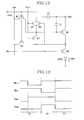
- FIG. 2shows a conventional voltage programming type pixel circuit for driving an organic EL element, representing one of N ⁇ M pixels.
- transistor M 1is coupled to an organic EL element (referred to as an OLED hereinafter) to thus supply current for light emission.
- the current of transistor M 1is controlled by a data voltage applied through switching transistor M 2 .
- capacitor C 1 for maintaining the applied voltage for a predetermined periodis coupled between a source and a gate of transistor M 1 .
- Scan line S nis coupled to a gate of transistor M 2
- data line Dmis coupled to a source thereof.
- I OLEDis the current flowing to the OLED
- V GSis a voltage between the source and the gate of transistor M 1
- V THis a threshold voltage at transistor M 1
- ⁇is a constant.
- the current corresponding to the applied data voltageis supplied to the OLED, and the OLED gives light in correspondence to the supplied current, according to the pixel circuit of FIG. 2.
- the applied data voltagehas multi-stage values within a predetermined range so as to represent gray.
- the conventional pixel circuit following the voltage programming methodhas a problem in that it is difficult to obtain high gray because of deviation of a threshold voltage V TH of a TFT and deviations of electron mobility caused by non-uniformity of an assembly process.
- V THthreshold voltage
- V 2568-bit
- the pixel circuit of the current programming methodcan achieve uniform display features even though a driving transistor in each pixel has non-uniform voltage-current characteristics.
- FIG. 3shows a pixel circuit of a conventional current programming method for driving the OLED, representing one of N ⁇ M pixels.
- transistor M 1is coupled to the OLED to supply the current for light emission, and the current of transistor M 1 is controlled by the data current applied through transistor M 2 .
- V GSis a voltage between the source and the gate of transistor M 1
- V THis a threshold voltage at transistor M 1
- ⁇is a constant
- a light emitting displayis provided for compensating for the threshold voltage of transistors or for electron mobility, and sufficiently charging the data line.
- a light emitting displayincludes a display panel on which a plurality of data lines for transmitting the data current that displays video signals, a plurality of scan lines for transmitting a select signal, and a plurality of pixel circuits formed at a plurality of pixels defined by the data lines and the scan lines are formed.
- the pixel circuitincludes: a light emitting element for emitting light corresponding to the applied current; a first transistor, having first and second main electrodes and a control electrode, for supplying a driving current for the light emitting element; a first switch for diode-connecting the first transistor in response to a first control signal; a first storage unit for storing a first voltage corresponding to a threshold voltage of the first transistor in response to a second control signal; a second switch for transmitting a data signal from the data line in response to the select signal from the scan line; a second storage unit for storing a second voltage corresponding to the data current from the first switch; and a third switch for transmitting the driving current from the first transistor to the light emitting element in response to a third control signal.
- a third voltage determined by coupling of the first and second storage units respectively storing the first and second voltagesis applied to the first transistor to supply the driving current to the light emitting element.
- the second control signalis enabled, the select signal is enabled, and the third control signal is then enabled in order.
- the pixel circuitfurther includes a fourth switch turned on in response to the second control signal, and coupled to a control electrode of the first transistor.
- the second storage unitis formed by a first capacitor coupled between the control electrode and the first main electrode of the first transistor.
- the first storage unitis formed by parallel coupling of a second capacitor coupled between the first main electrode of the first transistor and a second end of the fourth switch, and the first capacitor.
- the second control signalis the select signal from the scan line, and the fourth switch responds in the disable interval of the select signal.
- the first control signalincludes a select signal from the previous scan line and a select signal from the current scan line.
- the first switchincludes a second transistor for diode-connecting the first transistor in response to the select signal from the previous scan line, and a third transistor for diode-connecting the first transistor in response to the select signal from the current scan line.
- the second control signalincludes a select signal from the previous scan line, and the third control signal.
- the pixel circuitfurther includes a fifth switch coupled in parallel to the fourth switch. The fourth and fifth transistors are respectively turned on in response to the select signal from the previous scan line and the third control signal.
- a display panel of a light emitting displayon which a plurality of data lines for transmitting the data current that displays video signals, a plurality of scan lines for transmitting a select signal, and a plurality of pixel circuits formed at a plurality of pixels defined by the data lines and the scan lines are formed.
- the pixel circuitincludes: a first transistor having a first main electrode coupled to a first power supplying a first voltage; a first switch coupled between a second main electrode of the first transistor and the data line, and being controlled by a first select signal from the scan line; a second switch controlled by a first control signal to diode-connect the first transistor; a third switch having a first end coupled to a control electrode of the first transistor, and being controlled by a second control signal; a fourth switch having a first end coupled to a second main electrode of the first transistor, and being controlled by a third control signal; a light emitting element, coupled between a second end of the fourth switch and a second power supplying a second voltage, for emitting light corresponding to the applied current; a first storage unit coupled between the control electrode and the first main electrode of the first transistor when the third switch is turned on; and a second storage unit coupled between the control electrode and the first main electrode of the first transistor when the third switch is turned off.
- a method for driving a light emitting displayincluding a pixel circuit including a switch for transmitting a data current from a data line in response to a select signal from a scan line, a transistor including first and second main electrodes and a control electrode for outputting the driving current in response to the data current, and a light emitting element for emitting light corresponding to the driving current from the transistor.
- a first voltage corresponding to a threshold voltage of the transistoris stored in a first storage unit formed between the control electrode and the first main electrode of the transistor.
- a second voltage corresponding to the data current from the switchis stored in a second storage unit formed between the control electrode and the first main electrode of the transistor.
- the first and second storage unitsare coupled to establish the voltage between the control electrode and the first main electrode of the transistor as a third voltage.
- the driving currentis transmitted from the transistor to the light emitting display, wherein the driving current from the transistor is determined corresponding to the third voltage.
- a method for driving a light emitting displayincluding a pixel circuit including a switch for transmitting a data current from a data line in response to a select signal from a scan line, a transistor including first and second main electrodes and a control electrode for outputting the driving current in response to the data current, and a light emitting element for emitting light corresponding to the driving current from the transistor.
- the transistoris diode-connected in response to a first control signal.
- a first storage unitis coupled between the control electrode and the first main electrode of the transistor in response to a first level of a second control signal to store a first voltage corresponding to a threshold voltage of the transistor in the first storage unit.
- the transistoris diode-connected by the first control signal.
- a second storage unitis coupled between the control electrode and the first main electrode of the transistor in response to a second level of the second control signal.
- a second voltage corresponding to the data currentis stored in the second storage unit in response to the first select signal.
- the first and second storage unitsare coupled in response to the first level of the second control signal to establish the voltage between the control electrode and the first main electrode of the transistor as a third voltage.
- a driving currentis provided corresponding to the third voltage to the transistor.
- the driving currentis provided to the light emitting element in response to a third control signal.
- a method for driving a light emitting displayin a method for transmitting a data current showing video signals to a transistor in response to a first select signal to drive a light emitting element, a method for driving a light emitting display is provided.
- First and second control signalsare established respectively applied to first and second switches as an enable level to store a first voltage corresponding to a threshold voltage of the transistor.
- a third control signalis established applied to a third switch as a disable level to electrically intercept the transistor and the light emitting element.
- the first select signalis established as a disable level to intercept the data current.
- the first select signalis established as an enable level to supply the data current.
- the first and second control signalsare respectively established as enable and disable levels to store a second voltage corresponding to the data current.
- the first select signalis established as a disable level to intercept the data current.
- the first and second control signalsare respectively established as disable and enable levels to apply a third voltage to a main electrode and a gate electrode of the transistor.
- the third control signalis established as an enable level to transmit the current from the transistor to the light emitting element, wherein the third voltage is determined by the first and second voltages.
- FIG. 1shows a concept diagram of an OLED.
- FIG. 2shows an equivalent circuit of a conventional pixel circuit following the voltage programming method.
- FIG. 3shows an equivalent circuit of a conventional pixel circuit following the current programming method.
- FIG. 4shows a brief plane diagram of an organic EL display according to an embodiment of the present invention
- FIGS. 5, 7, 9 , 11 , 13 , 14 , and 15respectively show an equivalent circuit of a pixel circuit according to first through seventh embodiments of the present invention.
- FIGS. 6, 8, 10 , 12 , and 16respectively show a driving waveform for driving the pixel circuit of FIGS. 5, 7, 9 , 11 , and 15 .
- FIG. 4shows a brief ground plan of the OLED.
- the organic EL displayincludes organic EL display panel 10 , scan driver 20 , and data driver 30 .
- Organic EL display panel 10includes a plurality of data lines D 1 through D m in the row direction, a plurality of scan lines S 1 through S n , E 1 through E n , X 1 through X n , and Y 1 through Y n , and a plurality of pixel circuits 11 .
- Data lines D 1 through D mtransmit data signals that represent video signals to pixel circuit 11
- scan lines S 1 through S ntransmit select signals to pixel circuit 11 .
- Pixel circuit 11is formed at a pixel region defined by two adjacent data lines D 1 through D m and two adjacent scan lines S 1 through S n .
- scan lines E 1 through E ntransmit emit signals for controlling emission of pixel circuits 11
- scan lines X 1 through X n and Y 1 through Y nrespectively transmit control signals for controlling operation of pixel circuits 11 .
- Scan driver 20sequentially applies respective select signals and emit signals to scan lines S 1 through S n and E 1 through E n , and control signals to scan lines X 1 through X n and Y 1 through Y n .
- Data driver 30applies the data current that represents video signals to data lines D 1 through D m .
- Scan driver 20 and/or data driver 30can be coupled to display panel 10 , or can be installed, in a chip format, in a tape carrier package (TCP) coupled to display panel 10 .
- TCPtape carrier package
- the samecan be attached to display panel 10 , and installed, in a chip format, on a flexible printed circuit (FPC) or a film coupled to display panel 10 , which is referred to as a chip on flexible (CoF) board, or chip on film method.
- FPCflexible printed circuit
- CoFchip on flexible
- scan driver 20 and/or data driver 30can be installed on the glass substrate of the display panel, and further, the same can be substituted for the driving circuit formed in the same layers of the scan lines, the data lines, and TFTs on the glass substrate, or directly installed on the glass substrate, which is referred to as a chip on glass (CoG) method.
- CoGchip on glass
- FIG. 5shows an equivalent circuit diagram of the pixel circuit according to the first embodiment
- FIG. 6shows a driving waveform diagram for driving the pixel circuit of FIG. 5.
- FIG. 5shows a pixel circuit coupled to an m-th data line D m and an n-th scan line S n .
- pixel circuit 11includes an OLED, PMOS transistors M 1 through M 5 , and capacitors C 1 and C 2 .
- the transistoris preferably a thin film transistor having a gate electrode, a drain electrode, and a source electrode formed on the glass substrate as a control electrode and two main electrodes.
- Transistor M 1has a source coupled to power supply voltage VDD, and a gate coupled to transistor M 5 , and transistor M 3 is coupled between the gate and a drain of transistor M 1 .
- Transistor M 1outputs current I OLED corresponding to a voltage V GS at the gate and the source thereof.
- Transistor M 3diode-connects transistor M 1 in response to a control signal CS 1 n from scan line X n .
- Capacitor C 1is coupled between power supply voltage VDD and the gate of transistor M 1
- capacitor C 2is coupled between power supply voltage VDD and a first end of transistor M 5 .
- Capacitors C 1 and C 2operate as storage elements for storing the voltage between the gate and the source of the transistor.
- a second end of transistor M 5is coupled to the gate of transistor M 1 , and transistor M 5 couples capacitors C 1 and C 2 in response to a control signal CS 2 n from scan line Y n .
- Transistor M 2transmits data current I DATA from data line D m to transistor M 1 in response to a select signal SE n from scan line S n .
- Transistor M 4coupled between the drain of transistor M 1 and the OLED, transmits current I OLED of transistor M 1 to the OLED in response to an emit signal EM n of scan line E n .
- the OLEDis coupled between transistor M 4 and the reference voltage, and emits light corresponding to applied current I OLED .
- transistor M 5is turned on because of low-level control signal CS 2 n , and capacitors C 1 and C 2 are coupled in parallel between the gate and the source of transistor M 1 .
- Transistor M 3is turned on because of low-level control signal CS 1 n , transistor M 1 is diode-connected, and the threshold voltage V TH of transistor M 1 is stored in capacitors C 1 and C 2 coupled in parallel because of diode-connected transistor M 1 .
- Transistor M 4is turned off because of high-level emit signal EM n , and the current to the OLED is intercepted. That is, in interval T 1 , the threshold voltage V TH of transistor M 1 is sampled to capacitors C 1 and C 2 .
- control signal CS 2 nbecomes high level to turn off transistor M 5
- select signal SE nbecomes low level to turn on transistor M 2
- Capacitor C 2is floated while charged with voltage, because of turned-off transistor M 5 .
- Data current I DATA from data line D mflows to transistor M 1 because of turned-on transistor M 2 .
- the gate-source voltage V GS (T 2 ) at transistor M 1is determined corresponding to data current I DATA
- the gate-source voltage V GS (T 2 )is stored in capacitor C 1 .
- data current I DATAflows to transistor M 1 , data current I DATA can be expressed as Equation 3, and the gate-source voltage V GS (T 2 ) in interval T 2 is given as Equation 4 derived from Equation 3. That is, the gate-source voltage corresponding to data current I DATA is programmed to capacitor C 1 of the pixel circuit in interval T 2 .
- transistors M 3 and M 2are turned off in response to high-level control signal CS 1 n and select signal SE n , and transistors M 5 and M 4 are turned off because of low-level control signal CS 2 n and emit signal EM n .
- the gate-source voltage V GS (T 3 ) at transistor M 1 in interval T 3becomes Equation 5 because of coupling of capacitors C 1 and C 2 .
- ⁇ V GS ⁇ ( T3 ) ⁇⁇ V TH ⁇ + C 1 C 1 + C 2 ⁇ ( ⁇ V GS ⁇ ( T2 ) ⁇ - ⁇ V TH ⁇ ) Equation ⁇ ⁇ 5
- C 1 and C 2are respectively the capacitance of capacitors C 1 and C 2 .
- PMOS transistorsare used for transistors M 1 through M 5 .
- NMOS transistorscan also be implemented, which will now be described referring to FIGS. 7 and 8.
- FIG. 7shows an equivalent circuit diagram of the pixel circuit according to a second embodiment of the present invention
- FIG. 8shows a driving waveform diagram for driving the pixel circuit of FIG. 7.
- the pixel circuit of FIG. 7includes NMOS transistors M 1 through M 5 , and their coupling structure is symmetric with the pixel circuit of FIG. 5.
- transistor M 1has a source coupled to the reference voltage, a gate coupled to transistor M 5 , and transistor M 3 is coupled between the gate and a drain of transistor M 1 .
- Capacitor C 1is coupled between the reference voltage and the gate of transistor M 1
- capacitor C 2is coupled between the reference voltage and a first end of transistor M 5 .
- a second end of transistor M 5is coupled to the gate of transistor M 1 , and control signals CS 1 n and CS 2 n from scan lines X n and Y n are respectively applied to the gates of transistors M 3 and M 5 .
- Transistor M 2transmits data current I DATA from data line D m to transistor M 1 in response to select signal SE n from scan line S n .
- Transistor M 4is coupled between the drain of transistor M 1 and the OLED, and emit signal EM n from scan line E n is applied to the gate of transistor M 4 .
- the OLEDis coupled between transistor M 4 and power supply voltage VDD.
- the driving waveform for driving the pixel circuit of FIG. 7has an inverse form of the driving waveform of FIG. 6, as shown in FIG. 8. Since the detailed operation of the pixel circuit according to the second embodiment of the present invention can be easily obtained from the description of the first embodiment and FIGS. 7 and 8, no further detailed description will be provided.
- transistors M 1 through M 5are the same type transistors, a process for forming TFTs on the glass substrate of display panel 10 can be easily executed.
- Transistors M 1 through M 5are PMOS or NMOS types in the first and second embodiments, but without being restricted to this, they can be realized using combination of PMOS and NMOS transistors, or other switches having similar functions.
- Two control signals CS 1 n and CS 2 nare used to control the pixel circuit in the first and second embodiments, and in addition, the pixel circuit can be controlled using a single control signal, which will now be described with reference to FIGS. 9 through 12.
- FIG. 9shows an equivalent circuit diagram of the pixel circuit according to a third embodiment of the present invention
- FIG. 10shows a driving waveform diagram for driving the pixel circuit of FIG. 9.
- the pixel circuithas the same configuration as the first embodiment except for transistors M 2 and M 5 .
- Transistor M 2includes an NMOS transistor, and gates of transistors M 2 and M 5 are coupled in common to scan line S n . That is, transistor M 5 is driven by select signal SE n from scan line S n .
- transistors M 3 and M 5are turned on because of low-level control signal CS 1 n and select signal SE n .
- Transistor M 1is diode-connected because of turned-on transistor M 3 , and the threshold voltage V TH at transistor M 1 is stored in capacitors C 1 and C 2 .
- transistor M 4is turned off because of high-level emit signal EM n , and the current flow to the OLED is intercepted.
- select signal SE nbecomes high level to turn transistor M 2 on and transistor M 5 off. Then, the voltage V GS (T 2 ) expressed in Equation 4 is charged in capacitor C 1 . In this instance, since the voltage charged in capacitor C 2 can be changed when transistor M 2 is turned on because of select signal SE n , in order to prevent this, transistor M 3 is turned off before transistor M 2 is turned on, and again, transistor M 3 is turned on after transistor M 2 is turned on. That is, control signal CS 1 n is inverted to high level for a short time before select signal SE n becomes high level.
- scan lines Y 1 through Y n for supplying control signal CS 2 ncan be removed, thereby increasing the aperture ratio of the pixels.
- transistors M 1 and M 3 through M 5are realized with PMOS transistors, and transistor M 2 with an NMOS transistor, and further, the opposite realization of the transistors are possible, which will be described with reference to FIGS. 11 and 12.
- FIG. 11shows an equivalent circuit diagram of the pixel circuit according to a fourth embodiment of the present invention
- FIG. 12shows a driving waveform diagram for driving the pixel circuit of FIG. 11.
- the pixel circuitrealizes transistor M 2 with a PMOS transistor, and transistors M 1 and M 3 through M 5 with NMOS transistors, and their coupling structure is symmetric with that of the pixel circuit of FIG. 9.
- the driving waveform for driving the pixel circuit of FIG. 11has an inverse form of that of FIG. 10. Since the coupling structure and the operation of the pixel circuit according to the fourth embodiment can be easily obtained from the description of the third embodiment, no detailed description will be provided.
- capacitors C 1 and C 2are coupled in parallel to power supply voltage VDD, and differing from this, capacitors C 1 and C 2 can be coupled in series to power supply voltage VDD, which will now be described referring to FIGS. 13 and 14.
- FIG. 13shows an equivalent circuit diagram of the pixel circuit according to a fifth embodiment of the present invention.
- the pixel circuithas the same structure as that of the first embodiment except for the coupling states of capacitors C 1 and C 2 , and transistor M 5 .
- capacitors C 1 and C 2are coupled in series between power supply voltage VDD and transistor M 3
- transistor M 5is coupled between the common node of capacitors C 1 and C 2 and the gate of transistor M 1 .
- the pixel circuit according to the fifth embodimentis driven with the same driving waveform as that of the first embodiment, which will now be described referring to FIGS. 6 and 13.
- transistor M 3is turned on because of low-level control signal CS 1 n to diode-connect transistor M 1 .
- the threshold voltage V TH of transistor M 1is stored in capacitor C 1 because of diode-connected transistor M 1 , and the voltage at capacitor C 2 becomes 0V.
- transistor M 4is turned off because of high-level emit signal EM n to intercept the current flow to the OLED.
- control signal CS 2 nbecomes high level to turn off transistor M 5
- select SE nbecomes low level to turn on transistor M 2
- Data current I DATA from data line D mflows to transistor M 1 because of turned-on transistor M 2
- the gate-source voltage V GS (T 2 ) at transistor M 1becomes as shown in Equation 4.
- the voltage V C1 at capacitor C 1 charging the threshold voltage V THbecomes as shown in Equation 7 because of coupling of capacitors C 1 and C 2 .
- V C1⁇ V TH ⁇ + C 2 C 1 + C 2 ⁇ ( ⁇ V GS ⁇ ( T2 ) ⁇ - ⁇ V TH ⁇ ) Equation ⁇ ⁇ 7
- transistors M 3 and M 2are turned off in response to high-level control signal CS 1 n and select signal SE n , and transistors M 5 and M 4 are turned on because of low-level control signal CS 2 n and emit signal EM n .
- transistor M 3is turned off, and transistor M 5 is turned on, the voltage V C1 at capacitor C 1 becomes the gate-source voltage V GS (T 3 ) of transistor M 1 . Therefore, current I OLED flowing to transistor M 1 becomes as shown in Equation 8, and current I OLED is supplied to the OLED according to transistor M 4 thereby emitting light.
- current I OLED supplied to the OLEDis determined with no relation to the threshold voltage V TH of transistor M 1 or the mobility. Also, since the fine current flowing to the OLED using data current I DATA that is (C 1 +C 2 )/C 2 squared times current I OLED can be controlled, high gray can be represented. By supplying large data current I DATA to data lines D 1 through D M , sufficient charging time of the data lines can be obtained.
- Transistors M 1 through M 5are realized with PMOS transistors in the fifth embodiment, and they can also be realized with NMOS transistors, which will now be described with reference to FIG. 14.
- FIG. 14shows an equivalent circuit diagram of the pixel circuit according to a sixth embodiment of the present invention.
- the pixel circuitrealizes transistors M 1 through M 5 with NMOS transistors, and their coupling structure is symmetric with that of the pixel circuit of FIG. 13.
- the driving waveform for driving the pixel circuit of FIG. 14has an inverse driving waveform of the pixel circuit of FIG. 14, and it is the same driving waveform as that of FIG. 8. Since the coupling structure and the operation of the pixel circuit according to the sixth embodiment can be easily derived from the description of the fifth embodiment, no further detailed description will be provided.
- Two or one control signalis used to control the pixel circuit in the first through sixth embodiments, and differing from this, the pixel circuit can be controlled by using a select signal of a previous scan line without using the control signal, which will now be described in detail with reference to FIGS. 15 and 16.
- FIG. 15shows an equivalent circuit diagram of the pixel circuit according to a seventh embodiment of the present invention
- FIG. 16shows a driving waveform diagram for driving the pixel circuit of FIG. 15.
- the pixel circuithas the same structure as that of the first embodiment except for transistors M 3 , M 5 , M 6 , and M 7 .
- transistor M 3diode-connects transistor M 1 in response to select signal SE n-1 from previous scan line S n-1
- transistor M 7diode-connects transistor M 1 in response to select signal SE n from current scan line S n .
- Transistor M 7is coupled between data line D m and the gate of transistor M 1 in FIG. 15, and it can also be coupled between the gate and the drain of transistor M 1 .
- Transistors M 5 and M 6are coupled in parallel between capacitor C 2 and the gate of transistor M 1 .
- Transistor M 5responds to select signal SE n-1 from previous scan line S n-1
- transistor M 6responds to emit signal EM n from scan line E n .
- transistors M 3 and M 5are turned on because of low-level select signal SE n-1 .
- Capacitors C 1 and C 2are coupled in parallel between the gate and the source of transistor M 1 because of turned-on transistor M 5 .
- Transistor M 1is diode-connected because of turned-on transistor M 3 to store the threshold voltage V TH of transistor M 1 in capacitors C 1 and C 2 coupled in parallel.
- Transistors M 2 , M 7 , M 4 , and M 6are turned off because of high-level select signal SE n and emit signal EM n .
- select signal SE n-1becomes high level to turn off transistor M 3
- transistor M 7is turned on because of low-level select signal SE n to diode-connect transistor M 1 and maintain the diode-connected state of transistor M 1 .
- Transistor M 5is turned off because of select signal SE n-1 to have capacitor C 2 be floated while storing the voltage.
- Transistor M 2is turned on because of select signal SE n to make data current I DATA from data line D m flow to transistor M 1 .
- the gate-source voltage V GS (T 2 ) of transistor M 1is determined corresponding to data current I DATA , and the gate-source voltage V GS (T 2 ) is given as Equation 4 in the same manner of the first embodiment.
- select signal SE nbecomes high level to turn off transistors M 2 and M 7 , and transistors M 4 and M 6 are turned off because of low-level emit signal EM n .
- the gate-source voltage V GS (T 3 ) of transistor M 1is given as Equation 5 because of coupling of capacitors C 1 and C 2 in the like manner of the first embodiment. Therefore, current I OLED shown in Equation 6 is supplied to the OLED because of turned-on transistor M 4 to emit light.
- control signals CS 1 n and CS 2 nare removed in the seventh embodiment, and differing from this, one of control signals CS 1 n and CS 2 n can be removed.
- transistor M 7is removed from the pixel circuit of FIG. 15, and transistor M 3 is driven by not select signal SE n-1 but by control signal CS 1 n .
- transistor M 6is removed from the pixel circuit of FIG. 15, and transistor M 5 is not driven by the select signal SE n-1 and emit signal EM n but by control signal CS 2 n . Accordingly, the number of wires increases compared to FIG. 15, but the number of transistors can be reduced.
- PMOS and/or NMOS transistorsare used to realize a pixel circuit in the first through seventh embodiments, and without being restricted to this, the pixel circuit can be realized by PMOS transistors, NMOS transistors, or a combination of PMOS and NMOS transistors, and by other switches having similar functions.
- the current flowing to the OLEDcan be controlled using the large data current, the data line can be sufficiently charged during a single line time frame. Also, the deviation of the threshold voltage of the transistor or the deviation of the mobility is corrected, and a light emission display with high resolution and a wide screen can be realized.
Landscapes
- Engineering & Computer Science (AREA)
- Physics & Mathematics (AREA)
- Computer Hardware Design (AREA)
- General Physics & Mathematics (AREA)
- Theoretical Computer Science (AREA)
- Control Of Indicators Other Than Cathode Ray Tubes (AREA)
- Control Of El Displays (AREA)
- Electroluminescent Light Sources (AREA)
- Shift Register Type Memory (AREA)
- Illuminated Signs And Luminous Advertising (AREA)
Abstract
Description
- This application claims priority to and the benefit of Korea Patent Application No. 2003-20432 filed on Apr. 1, 2003 in the Korean Intellectual Property Office, the content of which is incorporated herein by reference.[0001]
- (a) Field of the Invention[0002]
- The present invention relates to a light emitting display, a display panel, and a driving method thereof. More specifically, the present invention relates to an organic electroluminescent (EL) display.[0003]
- (b) Description of the Related Art[0004]
- In general, an organic EL display electrically excites a phosphorous organic compound to emit light, and it voltage- or current-drives N×M organic emitting cells to display images. As shown in FIG. 1, the organic emitting cell includes an anode of indium tin oxide (ITO), an organic thin film, and a cathode layer of metal. The organic thin film has a multi-layer structure including an emitting layer (EML), an electron transport layer (ETL), and a hole transport layer (HTL) for maintaining balance between electrons and holes and improving emitting efficiencies, and it further includes an electron injecting layer (EIL) and a hole injecting layer (HIL).[0005]
- Methods for driving the organic emitting cells include the passive matrix method, and the active matrix method using thin film transistors (TFTs) or metal oxide semiconductor field effect transistors (MOSFETs). The passive matrix method forms cathodes and anodes to cross with each other, and selectively drives lines. The active matrix method connects a TFT and a capacitor with each ITO pixel electrode to thereby maintain a predetermined voltage according to capacitance. The active matrix method is classified as a voltage programming method or a current programming method according to signal forms supplied for maintaining a voltage at a capacitor.[0006]
- Referring to FIGS. 2 and 3, conventional organic EL displays of the voltage programming and current programming methods will be described.[0007]
- FIG. 2 shows a conventional voltage programming type pixel circuit for driving an organic EL element, representing one of N×M pixels. Referring to FIG. 2, transistor M[0008]1 is coupled to an organic EL element (referred to as an OLED hereinafter) to thus supply current for light emission. The current of transistor M1 is controlled by a data voltage applied through switching transistor M2. In this instance, capacitor C1 for maintaining the applied voltage for a predetermined period is coupled between a source and a gate of transistor M1. Scan line Snis coupled to a gate of transistor M2, and data line Dm is coupled to a source thereof.
- As to an operation of the above-configured pixel, when transistor M[0009]2 is turned on according to a select signal applied to the gate of switching transistor M2, a data voltage from data line Dm is applied to the gate of transistor M1. Accordingly, current IOLEDflows to transistor M2 in correspondence to a voltage VGScharged between the gate and the source by capacitor C1, and the OLED emits light in correspondence to current IOLED.
- where I[0011]OLEDis the current flowing to the OLED, VGSis a voltage between the source and the gate of transistor M1, VTHis a threshold voltage at transistor M1, and β is a constant.
- As given in[0012]
Equation 1, the current corresponding to the applied data voltage is supplied to the OLED, and the OLED gives light in correspondence to the supplied current, according to the pixel circuit of FIG. 2. In this instance, the applied data voltage has multi-stage values within a predetermined range so as to represent gray. - However, the conventional pixel circuit following the voltage programming method has a problem in that it is difficult to obtain high gray because of deviation of a threshold voltage V[0013]THof a TFT and deviations of electron mobility caused by non-uniformity of an assembly process. For example, in the case of driving a TFT of a pixel through 3 volts (3V), voltages are to be supplied to the gate of the TFT for each interval of 12 mV (=3V/256) so as to represent 8-bit (256) grays, and if the threshold voltage of the TFT caused by the non-uniformity of the assembly process deviates, it is difficult to represent high gray. Also, since the value β in
Equation 1 changes because of the deviation of the mobility, it becomes even more difficult to represent the high gray. - On assuming that the current source for supplying the current to the pixel circuit is uniform over the whole panel, the pixel circuit of the current programming method can achieve uniform display features even though a driving transistor in each pixel has non-uniform voltage-current characteristics.[0014]
- FIG. 3 shows a pixel circuit of a conventional current programming method for driving the OLED, representing one of N×M pixels. Referring to FIG. 3, transistor M[0015]1 is coupled to the OLED to supply the current for light emission, and the current of transistor M1 is controlled by the data current applied through transistor M2.
- First, when transistors M[0016]2 and M3 are turned on because of the select signal from scan line Sn, transistor M1 becomes diode-connected, and the voltage matched with data current IDATAfrom data line Dm is stored in capacitor C1. Next, the select signal from scan line Snbecomes high-level to turn on transistor M4. Then, the power is supplied from power supply voltage VDD, and the current matched with the voltage stored in capacitor C1 flows to the OLED to emit light. In this instance, the current flowing to the OLED is as follows.

- where V[0017]GSis a voltage between the source and the gate of transistor M1, VTHis a threshold voltage at transistor M1, and β is a constant.
- As given in Equation 2, since current I[0018]OLEDflowing to the OLED is the same as data current IDATAin the conventional current pixel circuit, uniform characteristics can be obtained when the programming current source is set to be uniform over the whole panel. However, since current IOLEDflowing to the OLED is a fine current, control over the pixel circuit by fine current IDATAproblematically requires much time to charge the data line. For example, assuming that the load capacitance of the data line is 30 pF, it requires several milliseconds of time to charge the load of the data line with the data current of several tens to hundreds of nA. This causes a problem that the charging time is not sufficient in consideration of the line time of several tens of microseconds.
- In accordance with the present invention a light emitting display is provided for compensating for the threshold voltage of transistors or for electron mobility, and sufficiently charging the data line.[0019]
- In one aspect of the present invention, a light emitting display is provided that includes a display panel on which a plurality of data lines for transmitting the data current that displays video signals, a plurality of scan lines for transmitting a select signal, and a plurality of pixel circuits formed at a plurality of pixels defined by the data lines and the scan lines are formed. The pixel circuit includes: a light emitting element for emitting light corresponding to the applied current; a first transistor, having first and second main electrodes and a control electrode, for supplying a driving current for the light emitting element; a first switch for diode-connecting the first transistor in response to a first control signal; a first storage unit for storing a first voltage corresponding to a threshold voltage of the first transistor in response to a second control signal; a second switch for transmitting a data signal from the data line in response to the select signal from the scan line; a second storage unit for storing a second voltage corresponding to the data current from the first switch; and a third switch for transmitting the driving current from the first transistor to the light emitting element in response to a third control signal. A third voltage determined by coupling of the first and second storage units respectively storing the first and second voltages is applied to the first transistor to supply the driving current to the light emitting element. The second control signal is enabled, the select signal is enabled, and the third control signal is then enabled in order. The pixel circuit further includes a fourth switch turned on in response to the second control signal, and coupled to a control electrode of the first transistor. The second storage unit is formed by a first capacitor coupled between the control electrode and the first main electrode of the first transistor. The first storage unit is formed by parallel coupling of a second capacitor coupled between the first main electrode of the first transistor and a second end of the fourth switch, and the first capacitor. The second control signal is the select signal from the scan line, and the fourth switch responds in the disable interval of the select signal. The first control signal includes a select signal from the previous scan line and a select signal from the current scan line. The first switch includes a second transistor for diode-connecting the first transistor in response to the select signal from the previous scan line, and a third transistor for diode-connecting the first transistor in response to the select signal from the current scan line. The second control signal includes a select signal from the previous scan line, and the third control signal. The pixel circuit further includes a fifth switch coupled in parallel to the fourth switch. The fourth and fifth transistors are respectively turned on in response to the select signal from the previous scan line and the third control signal.[0020]
- In another aspect of the present invention, a display panel of a light emitting display, on which a plurality of data lines for transmitting the data current that displays video signals, a plurality of scan lines for transmitting a select signal, and a plurality of pixel circuits formed at a plurality of pixels defined by the data lines and the scan lines are formed. The pixel circuit includes: a first transistor having a first main electrode coupled to a first power supplying a first voltage; a first switch coupled between a second main electrode of the first transistor and the data line, and being controlled by a first select signal from the scan line; a second switch controlled by a first control signal to diode-connect the first transistor; a third switch having a first end coupled to a control electrode of the first transistor, and being controlled by a second control signal; a fourth switch having a first end coupled to a second main electrode of the first transistor, and being controlled by a third control signal; a light emitting element, coupled between a second end of the fourth switch and a second power supplying a second voltage, for emitting light corresponding to the applied current; a first storage unit coupled between the control electrode and the first main electrode of the first transistor when the third switch is turned on; and a second storage unit coupled between the control electrode and the first main electrode of the first transistor when the third switch is turned off.[0021]
- In still another aspect of the present invention, a method is provided for driving a light emitting display including a pixel circuit including a switch for transmitting a data current from a data line in response to a select signal from a scan line, a transistor including first and second main electrodes and a control electrode for outputting the driving current in response to the data current, and a light emitting element for emitting light corresponding to the driving current from the transistor. A first voltage corresponding to a threshold voltage of the transistor is stored in a first storage unit formed between the control electrode and the first main electrode of the transistor. A second voltage corresponding to the data current from the switch is stored in a second storage unit formed between the control electrode and the first main electrode of the transistor. The first and second storage units are coupled to establish the voltage between the control electrode and the first main electrode of the transistor as a third voltage. The driving current is transmitted from the transistor to the light emitting display, wherein the driving current from the transistor is determined corresponding to the third voltage.[0022]
- In still yet another aspect of the present invention, a method is provided for driving a light emitting display including a pixel circuit including a switch for transmitting a data current from a data line in response to a select signal from a scan line, a transistor including first and second main electrodes and a control electrode for outputting the driving current in response to the data current, and a light emitting element for emitting light corresponding to the driving current from the transistor. The transistor is diode-connected in response to a first control signal. A first storage unit is coupled between the control electrode and the first main electrode of the transistor in response to a first level of a second control signal to store a first voltage corresponding to a threshold voltage of the transistor in the first storage unit. The transistor is diode-connected by the first control signal. A second storage unit is coupled between the control electrode and the first main electrode of the transistor in response to a second level of the second control signal. A second voltage corresponding to the data current is stored in the second storage unit in response to the first select signal. The first and second storage units are coupled in response to the first level of the second control signal to establish the voltage between the control electrode and the first main electrode of the transistor as a third voltage. A driving current is provided corresponding to the third voltage to the transistor. The driving current is provided to the light emitting element in response to a third control signal.[0023]
- In a still further another aspect of the present invention, in a method for transmitting a data current showing video signals to a transistor in response to a first select signal to drive a light emitting element, a method for driving a light emitting display is provided. First and second control signals are established respectively applied to first and second switches as an enable level to store a first voltage corresponding to a threshold voltage of the transistor. A third control signal is established applied to a third switch as a disable level to electrically intercept the transistor and the light emitting element. The first select signal is established as a disable level to intercept the data current. The first select signal is established as an enable level to supply the data current. The first and second control signals are respectively established as enable and disable levels to store a second voltage corresponding to the data current. The first select signal is established as a disable level to intercept the data current. The first and second control signals are respectively established as disable and enable levels to apply a third voltage to a main electrode and a gate electrode of the transistor. The third control signal is established as an enable level to transmit the current from the transistor to the light emitting element, wherein the third voltage is determined by the first and second voltages.[0024]
- FIG. 1 shows a concept diagram of an OLED.[0025]
- FIG. 2 shows an equivalent circuit of a conventional pixel circuit following the voltage programming method.[0026]
- FIG. 3 shows an equivalent circuit of a conventional pixel circuit following the current programming method.[0027]
- FIG. 4 shows a brief plane diagram of an organic EL display according to an embodiment of the present invention,[0028]
- FIGS. 5, 7,[0029]9,11,13,14, and15 respectively show an equivalent circuit of a pixel circuit according to first through seventh embodiments of the present invention.
- FIGS. 6, 8,[0030]10,12, and16 respectively show a driving waveform for driving the pixel circuit of FIGS. 5, 7,9,11, and15.
- An organic EL display, a corresponding pixel circuit, and a driving method thereof will be described in detail with reference to drawings.[0031]
- First, referring to FIG. 4, the organic EL display will be described. FIG. 4 shows a brief ground plan of the OLED.[0032]
- As shown, the organic EL display includes organic[0033]
EL display panel 10, scandriver 20, anddata driver 30. - Organic[0034]
EL display panel 10 includes a plurality of data lines D1through Dmin the row direction, a plurality of scan lines S1through Sn, E1through En, X1through Xn, and Y1through Yn, and a plurality ofpixel circuits 11. Data lines D1through Dmtransmit data signals that represent video signals topixel circuit 11, and scan lines S1through Sntransmit select signals topixel circuit 11.Pixel circuit 11 is formed at a pixel region defined by two adjacent data lines D1through Dmand two adjacent scan lines S1through Sn. Also, scan lines E1through Entransmit emit signals for controlling emission ofpixel circuits 11, and scan lines X1through Xnand Y1through Ynrespectively transmit control signals for controlling operation ofpixel circuits 11. - [0035]
Scan driver 20 sequentially applies respective select signals and emit signals to scan lines S1through Snand E1through En, and control signals to scan lines X1through Xnand Y1through Yn.Data driver 30 applies the data current that represents video signals to data lines D1through Dm. - [0036]
Scan driver 20 and/ordata driver 30 can be coupled todisplay panel 10, or can be installed, in a chip format, in a tape carrier package (TCP) coupled to displaypanel 10. The same can be attached to displaypanel 10, and installed, in a chip format, on a flexible printed circuit (FPC) or a film coupled to displaypanel 10, which is referred to as a chip on flexible (CoF) board, or chip on film method. Differing from this, scandriver 20 and/ordata driver 30 can be installed on the glass substrate of the display panel, and further, the same can be substituted for the driving circuit formed in the same layers of the scan lines, the data lines, and TFTs on the glass substrate, or directly installed on the glass substrate, which is referred to as a chip on glass (CoG) method. - Referring to FIGS. 5 and 6,[0037]
pixel circuit 11 of the organic EL display according to the first embodiment of the present invention will now be described. FIG. 5 shows an equivalent circuit diagram of the pixel circuit according to the first embodiment, and FIG. 6 shows a driving waveform diagram for driving the pixel circuit of FIG. 5. In this instance, for ease of description, FIG. 5 shows a pixel circuit coupled to an m-th data line Dmand an n-th scan line Sn. - As shown in FIG. 5,[0038]
pixel circuit 11 includes an OLED, PMOS transistors M1 through M5, and capacitors C1 and C2. The transistor is preferably a thin film transistor having a gate electrode, a drain electrode, and a source electrode formed on the glass substrate as a control electrode and two main electrodes. - Transistor M[0039]1 has a source coupled to power supply voltage VDD, and a gate coupled to transistor M5, and transistor M3 is coupled between the gate and a drain of transistor M1. Transistor M1 outputs current IOLEDcorresponding to a voltage VGSat the gate and the source thereof. Transistor M3 diode-connects transistor M1 in response to a control signal CS1nfrom scan line Xn. Capacitor C1 is coupled between power supply voltage VDD and the gate of transistor M1, and capacitor C2 is coupled between power supply voltage VDD and a first end of transistor M5. Capacitors C1 and C2 operate as storage elements for storing the voltage between the gate and the source of the transistor. A second end of transistor M5 is coupled to the gate of transistor M1, and transistor M5 couples capacitors C1 and C2 in response to a control signal CS2nfrom scan line Yn.
- Transistor M[0040]2 transmits data current IDATAfrom data line Dmto transistor M1 in response to a select signal SEnfrom scan line Sn. Transistor M4 coupled between the drain of transistor M1 and the OLED, transmits current IOLEDof transistor M1 to the OLED in response to an emit signal EMnof scan line En. The OLED is coupled between transistor M4 and the reference voltage, and emits light corresponding to applied current IOLED.
- Referring to FIG. 6, an operation of the pixel circuit according to the first embodiment of the present invention will now be described in detail.[0041]
- As shown, in interval T[0042]1, transistor M5 is turned on because of low-level control signal CS2n, and capacitors C1 and C2 are coupled in parallel between the gate and the source of transistor M1. Transistor M3 is turned on because of low-level control signal CS1n, transistor M1 is diode-connected, and the threshold voltage VTHof transistor M1 is stored in capacitors C1 and C2 coupled in parallel because of diode-connected transistor M1. Transistor M4 is turned off because of high-level emit signal EMn, and the current to the OLED is intercepted. That is, in interval T1, the threshold voltage VTHof transistor M1 is sampled to capacitors C1 and C2.
- In interval T[0043]2, control signal CS2nbecomes high level to turn off transistor M5, and select signal SEnbecomes low level to turn on transistor M2. Capacitor C2 is floated while charged with voltage, because of turned-off transistor M5. Data current IDATAfrom data line Dmflows to transistor M1 because of turned-on transistor M2. Accordingly, the gate-source voltage VGS(T2) at transistor M1 is determined corresponding to data current IDATA, and the gate-source voltage VGS(T2) is stored in capacitor C1. Since data current IDATAflows to transistor M1, data current IDATAcan be expressed as Equation 3, and the gate-source voltage VGS(T2) in interval T2 is given as Equation 4 derived from Equation 3. That is, the gate-source voltage corresponding to data current IDATAis programmed to capacitor C1 of the pixel circuit in interval T2.


- where β is a constant.[0044]
- Next, in interval T[0045]3, transistors M3 and M2 are turned off in response to high-level control signal CS1nand select signal SEn, and transistors M5 and M4 are turned off because of low-level control signal CS2nand emit signal EMn. When transistor M5 is turned on, the gate-source voltage VGS(T3) at transistor M1 in interval T3 becomes Equation 5 because of coupling of capacitors C1 and C2.

- where C[0046]1 and C2 are respectively the capacitance of capacitors C1 and C2.
- As expressed in Equation 6, since current I[0048]OLEDsupplied to the OLED is determined with no relation to the threshold voltage VTHof transistor M1 or the mobility, the deviation of the threshold voltage or the deviation of the mobility can be corrected. Also, current IOLEDsupplied to the OLED is C1/(C1+C2) squared times smaller than the data current IDATA. For example, if C2 is M times greater than C1 (C2=M×C1), the fine current flowing to the OLED can be controlled by data current IDATAwhich is (M+1)2times greater than current IOLED, thereby enabling representation of high gray. Further, since the large data current IDATAis supplied to data lines D1through Dm, charging time for the data lines can be sufficiently obtained.
- In the first embodiment, PMOS transistors are used for transistors M[0049]1 through M5. However, NMOS transistors can also be implemented, which will now be described referring to FIGS. 7 and 8.
- FIG. 7 shows an equivalent circuit diagram of the pixel circuit according to a second embodiment of the present invention, and FIG. 8 shows a driving waveform diagram for driving the pixel circuit of FIG. 7.[0050]
- The pixel circuit of FIG. 7 includes NMOS transistors M[0051]1 through M5, and their coupling structure is symmetric with the pixel circuit of FIG. 5. In detail, transistor M1 has a source coupled to the reference voltage, a gate coupled to transistor M5, and transistor M3 is coupled between the gate and a drain of transistor M1. Capacitor C1 is coupled between the reference voltage and the gate of transistor M1, and capacitor C2 is coupled between the reference voltage and a first end of transistor M5. A second end of transistor M5 is coupled to the gate of transistor M1, and control signals CS1nand CS2nfrom scan lines Xnand Ynare respectively applied to the gates of transistors M3 and M5. Transistor M2 transmits data current IDATAfrom data line Dmto transistor M1 in response to select signal SEnfrom scan line Sn. Transistor M4 is coupled between the drain of transistor M1 and the OLED, and emit signal EMnfrom scan line Enis applied to the gate of transistor M4. The OLED is coupled between transistor M4 and power supply voltage VDD.
- Since the pixel circuit of FIG. 7 includes NMOS transistors, the driving waveform for driving the pixel circuit of FIG. 7 has an inverse form of the driving waveform of FIG. 6, as shown in FIG. 8. Since the detailed operation of the pixel circuit according to the second embodiment of the present invention can be easily obtained from the description of the first embodiment and FIGS. 7 and 8, no further detailed description will be provided.[0052]
- According to the first and second embodiments, since transistors M[0053]1 through M5 are the same type transistors, a process for forming TFTs on the glass substrate of
display panel 10 can be easily executed. - Transistors M[0054]1 through M5 are PMOS or NMOS types in the first and second embodiments, but without being restricted to this, they can be realized using combination of PMOS and NMOS transistors, or other switches having similar functions.
- Two control signals CS[0055]1nand CS2nare used to control the pixel circuit in the first and second embodiments, and in addition, the pixel circuit can be controlled using a single control signal, which will now be described with reference to FIGS. 9 through 12.
- FIG. 9 shows an equivalent circuit diagram of the pixel circuit according to a third embodiment of the present invention, and FIG. 10 shows a driving waveform diagram for driving the pixel circuit of FIG. 9.[0056]
- As shown in FIG. 9, the pixel circuit has the same configuration as the first embodiment except for transistors M[0057]2 and M5. Transistor M2 includes an NMOS transistor, and gates of transistors M2 and M5 are coupled in common to scan line Sn. That is, transistor M5 is driven by select signal SEnfrom scan line Sn.
- Referring to FIG. 10, in interval T[0058]1, transistors M3 and M5 are turned on because of low-level control signal CS1nand select signal SEn. Transistor M1 is diode-connected because of turned-on transistor M3, and the threshold voltage VTHat transistor M1 is stored in capacitors C1 and C2. Also, transistor M4 is turned off because of high-level emit signal EMn, and the current flow to the OLED is intercepted.
- In interval T[0059]2, select signal SEnbecomes high level to turn transistor M2 on and transistor M5 off. Then, the voltage VGS(T2) expressed in Equation 4 is charged in capacitor C1. In this instance, since the voltage charged in capacitor C2 can be changed when transistor M2 is turned on because of select signal SEn, in order to prevent this, transistor M3 is turned off before transistor M2 is turned on, and again, transistor M3 is turned on after transistor M2 is turned on. That is, control signal CS1nis inverted to high level for a short time before select signal SEnbecomes high level.
- Since other operations in the third embodiment of the present invention are matched with those of the first embodiment, no further corresponding description will be provided. According to the third embodiment, scan lines Y[0060]1through Ynfor supplying control signal CS2ncan be removed, thereby increasing the aperture ratio of the pixels.
- In the third embodiment, transistors M[0061]1 and M3 through M5 are realized with PMOS transistors, and transistor M2 with an NMOS transistor, and further, the opposite realization of the transistors are possible, which will be described with reference to FIGS. 11 and 12.
- FIG. 11 shows an equivalent circuit diagram of the pixel circuit according to a fourth embodiment of the present invention, and FIG. 12 shows a driving waveform diagram for driving the pixel circuit of FIG. 11.[0062]
- As shown in FIG. 11, the pixel circuit realizes transistor M[0063]2 with a PMOS transistor, and transistors M1 and M3 through M5 with NMOS transistors, and their coupling structure is symmetric with that of the pixel circuit of FIG. 9. Also, as shown in FIG. 12, the driving waveform for driving the pixel circuit of FIG. 11 has an inverse form of that of FIG. 10. Since the coupling structure and the operation of the pixel circuit according to the fourth embodiment can be easily obtained from the description of the third embodiment, no detailed description will be provided.
- In the first through fourth embodiments, capacitors C[0064]1 and C2 are coupled in parallel to power supply voltage VDD, and differing from this, capacitors C1 and C2 can be coupled in series to power supply voltage VDD, which will now be described referring to FIGS. 13 and 14.
- FIG. 13 shows an equivalent circuit diagram of the pixel circuit according to a fifth embodiment of the present invention.[0065]
- As shown, the pixel circuit has the same structure as that of the first embodiment except for the coupling states of capacitors C[0066]1 and C2, and transistor M5. In detail, capacitors C1 and C2 are coupled in series between power supply voltage VDD and transistor M3, and transistor M5 is coupled between the common node of capacitors C1 and C2 and the gate of transistor M1.
- The pixel circuit according to the fifth embodiment is driven with the same driving waveform as that of the first embodiment, which will now be described referring to FIGS. 6 and 13.[0067]
- In interval T[0068]1, transistor M3 is turned on because of low-level control signal CS1nto diode-connect transistor M1. The threshold voltage VTHof transistor M1 is stored in capacitor C1 because of diode-connected transistor M1, and the voltage at capacitor C2 becomes 0V. Also, transistor M4 is turned off because of high-level emit signal EMnto intercept the current flow to the OLED.
- In interval T[0069]2, control signal CS2nbecomes high level to turn off transistor M5, and select SEnbecomes low level to turn on transistor M2. Data current IDATAfrom data line Dmflows to transistor M1 because of turned-on transistor M2, and the gate-source voltage VGS(T2) at transistor M1 becomes as shown in Equation 4. Hence, the voltage VC1at capacitor C1 charging the threshold voltage VTHbecomes as shown in Equation 7 because of coupling of capacitors C1 and C2.

- Next, in interval T[0070]3, transistors M3 and M2 are turned off in response to high-level control signal CS1nand select signal SEn, and transistors M5 and M4 are turned on because of low-level control signal CS2nand emit signal EMn. When transistor M3 is turned off, and transistor M5 is turned on, the voltage VC1at capacitor C1 becomes the gate-source voltage VGS(T3) of transistor M1. Therefore, current IOLEDflowing to transistor M1 becomes as shown in Equation 8, and current IOLEDis supplied to the OLED according to transistor M4 thereby emitting light.

- In the like manner of the first embodiment, current I[0071]OLEDsupplied to the OLED is determined with no relation to the threshold voltage VTHof transistor M1 or the mobility. Also, since the fine current flowing to the OLED using data current IDATAthat is (C1+C2)/C2 squared times current IOLEDcan be controlled, high gray can be represented. By supplying large data current IDATAto data lines D1through DM, sufficient charging time of the data lines can be obtained.
- Transistors M[0072]1 through M5 are realized with PMOS transistors in the fifth embodiment, and they can also be realized with NMOS transistors, which will now be described with reference to FIG. 14.
- FIG. 14 shows an equivalent circuit diagram of the pixel circuit according to a sixth embodiment of the present invention.[0073]
- As shown, the pixel circuit realizes transistors M[0074]1 through M5 with NMOS transistors, and their coupling structure is symmetric with that of the pixel circuit of FIG. 13. The driving waveform for driving the pixel circuit of FIG. 14 has an inverse driving waveform of the pixel circuit of FIG. 14, and it is the same driving waveform as that of FIG. 8. Since the coupling structure and the operation of the pixel circuit according to the sixth embodiment can be easily derived from the description of the fifth embodiment, no further detailed description will be provided.
- Two or one control signal is used to control the pixel circuit in the first through sixth embodiments, and differing from this, the pixel circuit can be controlled by using a select signal of a previous scan line without using the control signal, which will now be described in detail with reference to FIGS. 15 and 16.[0075]
- FIG. 15 shows an equivalent circuit diagram of the pixel circuit according to a seventh embodiment of the present invention, and FIG. 16 shows a driving waveform diagram for driving the pixel circuit of FIG. 15.[0076]
- As shown in FIG. 15, the pixel circuit has the same structure as that of the first embodiment except for transistors M[0077]3, M5, M6, and M7. In detail, transistor M3 diode-connects transistor M1 in response to select signal SEn-1from previous scan line Sn-1, and transistor M7 diode-connects transistor M1 in response to select signal SEnfrom current scan line Sn. Transistor M7 is coupled between data line Dmand the gate of transistor M1 in FIG. 15, and it can also be coupled between the gate and the drain of transistor M1. Transistors M5 and M6 are coupled in parallel between capacitor C2 and the gate of transistor M1. Transistor M5 responds to select signal SEn-1from previous scan line Sn-1, and transistor M6 responds to emit signal EMnfrom scan line En.
- Next, the operation of the pixel circuit of FIG. 15 will be described referring to FIG. 16.[0078]
- As shown, in interval T[0079]1, transistors M3 and M5 are turned on because of low-level select signal SEn-1. Capacitors C1 and C2 are coupled in parallel between the gate and the source of transistor M1 because of turned-on transistor M5. Transistor M1 is diode-connected because of turned-on transistor M3 to store the threshold voltage VTHof transistor M1 in capacitors C1 and C2 coupled in parallel. Transistors M2, M7, M4, and M6 are turned off because of high-level select signal SEnand emit signal EMn.
- In interval T[0080]2, select signal SEn-1becomes high level to turn off transistor M3, and transistor M7 is turned on because of low-level select signal SEnto diode-connect transistor M1 and maintain the diode-connected state of transistor M1. Transistor M5 is turned off because of select signal SEn-1to have capacitor C2 be floated while storing the voltage. Transistor M2 is turned on because of select signal SEnto make data current IDATAfrom data line Dmflow to transistor M1. The gate-source voltage VGS(T2) of transistor M1 is determined corresponding to data current IDATA, and the gate-source voltage VGS(T2) is given as Equation 4 in the same manner of the first embodiment.
- Next, in interval T[0081]3, select signal SEnbecomes high level to turn off transistors M2 and M7, and transistors M4 and M6 are turned off because of low-level emit signal EMn. When transistor M6 is turned on, the gate-source voltage VGS(T3) of transistor M1 is given as Equation 5 because of coupling of capacitors C1 and C2 in the like manner of the first embodiment. Therefore, current IOLEDshown in Equation 6 is supplied to the OLED because of turned-on transistor M4 to emit light.
- The two control signals CS[0082]1nand CS2nare removed in the seventh embodiment, and differing from this, one of control signals CS1nand CS2ncan be removed. In detail, in the case of additionally using control signal CS1nin the seventh embodiment, transistor M7 is removed from the pixel circuit of FIG. 15, and transistor M3 is driven by not select signal SEn-1but by control signal CS1n. In the case of additionally using control signal CS2nin the seventh embodiment, transistor M6 is removed from the pixel circuit of FIG. 15, and transistor M5 is not driven by the select signal SEn-1and emit signal EMnbut by control signal CS2n. Accordingly, the number of wires increases compared to FIG. 15, but the number of transistors can be reduced.
- In the above, PMOS and/or NMOS transistors are used to realize a pixel circuit in the first through seventh embodiments, and without being restricted to this, the pixel circuit can be realized by PMOS transistors, NMOS transistors, or a combination of PMOS and NMOS transistors, and by other switches having similar functions.[0083]
- Accordingly, since the current flowing to the OLED can be controlled using the large data current, the data line can be sufficiently charged during a single line time frame. Also, the deviation of the threshold voltage of the transistor or the deviation of the mobility is corrected, and a light emission display with high resolution and a wide screen can be realized.[0084]
- While this invention has been described in connection with what is presently considered to be practical embodiments, it is to be understood that the invention is not limited to the disclosed embodiments, but, on the contrary, is intended to cover various modifications and equivalent arrangements included within the spirit and scope of the appended claims.[0085]


Claims (40)
Priority Applications (5)
| Application Number | Priority Date | Filing Date | Title |
|---|---|---|---|
| US11/140,013US7573441B2 (en) | 2003-04-01 | 2005-05-27 | Light emitting display, display panel, and driving method thereof |
| US11/139,148US7518580B2 (en) | 2003-04-01 | 2005-05-27 | Light emitting display, display panel, and driving method thereof |
| US12/495,710US8289240B2 (en) | 2003-04-01 | 2009-06-30 | Light emitting display, display panel, and driving method thereof |
| US12/495,713US20090267935A1 (en) | 2003-04-01 | 2009-06-30 | Light emitting display, display panel, and driving method thereof |
| US12/495,715US8217863B2 (en) | 2003-04-01 | 2009-06-30 | Light emitting display, display panel, and driving method thereof |
Applications Claiming Priority (3)
| Application Number | Priority Date | Filing Date | Title |
|---|---|---|---|
| KR10-2003-0020432AKR100502912B1 (en) | 2003-04-01 | 2003-04-01 | Light emitting display device and display panel and driving method thereof |
| KR2003-0020432 | 2003-04-01 | ||
| KR10-2003-0020432 | 2003-04-01 |
Related Child Applications (2)
| Application Number | Title | Priority Date | Filing Date |
|---|---|---|---|
| US11/140,013ContinuationUS7573441B2 (en) | 2003-04-01 | 2005-05-27 | Light emitting display, display panel, and driving method thereof |
| US11/139,148ContinuationUS7518580B2 (en) | 2003-04-01 | 2005-05-27 | Light emitting display, display panel, and driving method thereof |
Publications (2)
| Publication Number | Publication Date |
|---|---|
| US20040196239A1true US20040196239A1 (en) | 2004-10-07 |
| US6919871B2 US6919871B2 (en) | 2005-07-19 |
Family
ID=32844897
Family Applications (6)
| Application Number | Title | Priority Date | Filing Date |
|---|---|---|---|
| US10/729,256Expired - LifetimeUS6919871B2 (en) | 2003-04-01 | 2003-12-04 | Light emitting display, display panel, and driving method thereof |
| US11/139,148Expired - LifetimeUS7518580B2 (en) | 2003-04-01 | 2005-05-27 | Light emitting display, display panel, and driving method thereof |
| US11/140,013Active2026-11-07US7573441B2 (en) | 2003-04-01 | 2005-05-27 | Light emitting display, display panel, and driving method thereof |
| US12/495,710Expired - LifetimeUS8289240B2 (en) | 2003-04-01 | 2009-06-30 | Light emitting display, display panel, and driving method thereof |
| US12/495,713AbandonedUS20090267935A1 (en) | 2003-04-01 | 2009-06-30 | Light emitting display, display panel, and driving method thereof |
| US12/495,715Expired - LifetimeUS8217863B2 (en) | 2003-04-01 | 2009-06-30 | Light emitting display, display panel, and driving method thereof |
Family Applications After (5)
| Application Number | Title | Priority Date | Filing Date |
|---|---|---|---|
| US11/139,148Expired - LifetimeUS7518580B2 (en) | 2003-04-01 | 2005-05-27 | Light emitting display, display panel, and driving method thereof |
| US11/140,013Active2026-11-07US7573441B2 (en) | 2003-04-01 | 2005-05-27 | Light emitting display, display panel, and driving method thereof |
| US12/495,710Expired - LifetimeUS8289240B2 (en) | 2003-04-01 | 2009-06-30 | Light emitting display, display panel, and driving method thereof |
| US12/495,713AbandonedUS20090267935A1 (en) | 2003-04-01 | 2009-06-30 | Light emitting display, display panel, and driving method thereof |
| US12/495,715Expired - LifetimeUS8217863B2 (en) | 2003-04-01 | 2009-06-30 | Light emitting display, display panel, and driving method thereof |
Country Status (7)
| Country | Link |
|---|---|
| US (6) | US6919871B2 (en) |
| EP (1) | EP1465143B1 (en) |
| JP (1) | JP4153842B2 (en) |
| KR (1) | KR100502912B1 (en) |
| CN (1) | CN100369096C (en) |
| AT (1) | ATE341069T1 (en) |
| DE (1) | DE60308641T2 (en) |
Cited By (49)
| Publication number | Priority date | Publication date | Assignee | Title |
|---|---|---|---|---|
| US20050062685A1 (en)* | 2003-06-09 | 2005-03-24 | Masashi Nogawa | Drive circuit and display system with said drive circuit |
| US20050140605A1 (en)* | 2003-11-24 | 2005-06-30 | Jin-Tae Jung | Image display device and driving method thereof |
| US20050219172A1 (en)* | 2004-03-30 | 2005-10-06 | Li-Wei Shih | Display array and display panel utilizing the same |
| US20060028409A1 (en)* | 2004-08-05 | 2006-02-09 | Takaji Numao | Display device and driving method thereof |
| US20060044230A1 (en)* | 2004-08-30 | 2006-03-02 | Ki-Myeong Eom | Signal driving method and apparatus for a light emitting display |
| US20060055336A1 (en)* | 2004-08-30 | 2006-03-16 | Jeong Jin T | Organic light emitting display |
| US20060145989A1 (en)* | 2004-12-03 | 2006-07-06 | Seoul National University Industry Foundation | Picture element structure of current programming method type active matrix organic emitting diode display and driving method of data line |
| US20060186822A1 (en)* | 2005-02-18 | 2006-08-24 | Samsung Sdi Co., Ltd. | Time-divisional driving organic electroluminescence display |
| US20060256057A1 (en)* | 2005-04-29 | 2006-11-16 | Min-Koo Han | Pixel structure using voltage programming-type for active matrix organic light emitting device |
| US20070018917A1 (en)* | 2005-07-15 | 2007-01-25 | Seiko Epson Corporation | Electronic device, method of driving the same, electro-optical device, and electronic apparatus |
| US20070040786A1 (en)* | 2005-08-17 | 2007-02-22 | Samsung Sdi Co., Ltd. | Emission control driver and organic light emitting display device having the same and a logical or circuit for an emission control driver for outputting an emission control signal |
| US20070046593A1 (en)* | 2005-08-26 | 2007-03-01 | Dong-Yong Shin | Organic light emitting diode display device and driving method thereof |
| US20070063935A1 (en)* | 2005-09-15 | 2007-03-22 | Semiconductor Energy Laboratory Co., Ltd. | Display device and driving method thereof |
| US20070124633A1 (en)* | 2005-11-09 | 2007-05-31 | Kim Yang W | Scan driver and organic light emitting display device |
| US20070200793A1 (en)* | 2006-02-28 | 2007-08-30 | Oh Kyong Kwon | Organic light emitting display device and driving method |
| US20070200814A1 (en)* | 2006-02-28 | 2007-08-30 | Oh Kyong Kwon | Organic light emitting display device and driving method |
| US20070268217A1 (en)* | 2006-05-18 | 2007-11-22 | Tae Joon Ahn | Pixel circuit of organic light emitting display |
| US20080042941A1 (en)* | 2006-08-16 | 2008-02-21 | Tpo Displays Corp. | System for displaying image and driving method for organic light-emitting element |
| US20080074412A1 (en)* | 2006-07-03 | 2008-03-27 | Seiko Epson Corporation | Light emitting device, method of driving pixel circuit, and driving circuit |
| US20080143653A1 (en)* | 2006-12-15 | 2008-06-19 | Semiconductor Energy Laboratory Co., Ltd. | Semiconductor device and driving method thereof |
| US20080158114A1 (en)* | 2006-12-27 | 2008-07-03 | Hyung-Soo Kim | Organic electroluminescent display device and method of driving the same |
| US20080238835A1 (en)* | 2007-03-30 | 2008-10-02 | Sony Corporation | Display apparatus and driving method therefor |
| CN100444230C (en)* | 2005-01-10 | 2008-12-17 | 三星Sdi株式会社 | Emission control driver and organic light emitting display using same |
| US20090101912A1 (en)* | 2007-10-23 | 2009-04-23 | Chunghwa Picture Tubes, Ltd. | Active device array for reducing delay of scan signal and flat panel display using the same |
| US20090135107A1 (en)* | 2007-11-23 | 2009-05-28 | Hyung-Soo Kim | Organic light emitting display |
| US20090273725A1 (en)* | 2008-04-30 | 2009-11-05 | Lu Ying-Chi | Liquid crystal display panel and pixel structure thereof |
| US20100110055A1 (en)* | 2007-12-19 | 2010-05-06 | Shinya Ono | Active matrix type display apparatus |
| US20100245219A1 (en)* | 2005-09-16 | 2010-09-30 | Semiconductor Energy Laboratory Co., Ltd. | Display device and driving method of display device |
| US7995009B2 (en) | 2005-09-16 | 2011-08-09 | Semiconductor Energy Laboratory Co., Ltd. | Display device having pixel including transistor and driving method of the same |
| US20110209567A1 (en)* | 2005-07-04 | 2011-09-01 | National University Corporation Tohoku University | Display apparatus |
| US20120062608A1 (en)* | 2010-09-14 | 2012-03-15 | Dong-Hwi Kim | Emission control driver and organic light emitting display using the same |
| US20120062525A1 (en)* | 2010-09-14 | 2012-03-15 | Dong-Hwi Kim | Scan driver and organic light emitting display using the same |
| US20130033475A1 (en)* | 2011-08-05 | 2013-02-07 | Semiconductor Energy Laboratory Co., Ltd. | Display Device |
| US20130113779A1 (en)* | 2011-11-08 | 2013-05-09 | Lg Display Co., Ltd. | Organic light emitting diode display device |
| US20130187554A1 (en)* | 2011-08-09 | 2013-07-25 | Panasonic Corporation | Image display device |
| US20140118653A1 (en)* | 2005-07-14 | 2014-05-01 | Semiconductor Energy Laboratory Co., Ltd. | Semiconductor device and driving method thereof |
| US20140168180A1 (en)* | 2012-12-13 | 2014-06-19 | Samsung Display Co., Ltd. | Pixel and organic light emitting display device using the same |
| CN103927969A (en)* | 2013-06-28 | 2014-07-16 | 上海天马微电子有限公司 | Pixel compensation circuit and display |
| TWI464724B (en)* | 2006-06-19 | 2014-12-11 | Seiko Epson Corp | Electronic circuit, method for driving the saem, electronic device, and electronic apparatus |
| US20150097762A1 (en)* | 2013-10-07 | 2015-04-09 | Samsung Display Co., Ltd. | Pixel and organic light emitting display using the same |
| US9105213B2 (en) | 2012-08-17 | 2015-08-11 | Lg Display Co., Ltd. | Organic light emitting diode display and method of driving the same |
| US9311852B2 (en)* | 2013-04-27 | 2016-04-12 | Boe Technology Group Co., Ltd. | Pixel circuit and organic light-emitting display comprising the same |
| US20160210896A1 (en)* | 2015-01-19 | 2016-07-21 | Samsung Display Co., Ltd. | Organic light-emitting diode display |
| US9734762B2 (en) | 2011-11-02 | 2017-08-15 | Sharp Kabushiki Kaisha | Color display device with pixel circuits including two capacitors |
| US20180286308A1 (en)* | 2017-04-04 | 2018-10-04 | Samsung Display Co., Ltd. | Organic light-emitting display device and method of driving the same |
| US20190156755A1 (en)* | 2017-11-20 | 2019-05-23 | Seiko Epson Corporation | Electro-optical device and electronic apparatus |
| CN109817161A (en)* | 2017-11-20 | 2019-05-28 | 精工爱普生株式会社 | Electro-optical devices and electronic equipment |
| US11069295B2 (en)* | 2018-10-04 | 2021-07-20 | Samsung Display Co., Ltd. | Display apparatus and method of driving display panel using the same |
| US11263980B2 (en)* | 2018-12-18 | 2022-03-01 | Samsung Display Co., Ltd. | Display apparatus and method of driving display panel using the same |
Families Citing this family (156)
| Publication number | Priority date | Publication date | Assignee | Title |
|---|---|---|---|---|
| US7569849B2 (en) | 2001-02-16 | 2009-08-04 | Ignis Innovation Inc. | Pixel driver circuit and pixel circuit having the pixel driver circuit |
| CA2419704A1 (en) | 2003-02-24 | 2004-08-24 | Ignis Innovation Inc. | Method of manufacturing a pixel with organic light-emitting diode |
| KR100502912B1 (en)* | 2003-04-01 | 2005-07-21 | 삼성에스디아이 주식회사 | Light emitting display device and display panel and driving method thereof |
| CA2443206A1 (en) | 2003-09-23 | 2005-03-23 | Ignis Innovation Inc. | Amoled display backplanes - pixel driver circuits, array architecture, and external compensation |
| JP4107240B2 (en)* | 2004-01-21 | 2008-06-25 | セイコーエプソン株式会社 | Driving circuit, electro-optical device, driving method of electro-optical device, and electronic apparatus |
| GB2411758A (en)* | 2004-03-04 | 2005-09-07 | Seiko Epson Corp | Pixel circuit |
| CA2472671A1 (en) | 2004-06-29 | 2005-12-29 | Ignis Innovation Inc. | Voltage-programming scheme for current-driven amoled displays |
| KR101087417B1 (en)* | 2004-08-13 | 2011-11-25 | 엘지디스플레이 주식회사 | Driving circuit of organic light emitting display |
| KR100592636B1 (en)* | 2004-10-08 | 2006-06-26 | 삼성에스디아이 주식회사 | LED display device |
| KR100606416B1 (en)* | 2004-11-17 | 2006-07-31 | 엘지.필립스 엘시디 주식회사 | Driving device and driving method of organic light emitting diode |
| KR100602352B1 (en)* | 2004-11-22 | 2006-07-18 | 삼성에스디아이 주식회사 | Pixel and light emitting display device using same |
| CA2490858A1 (en)* | 2004-12-07 | 2006-06-07 | Ignis Innovation Inc. | Driving method for compensated voltage-programming of amoled displays |
| US9799246B2 (en) | 2011-05-20 | 2017-10-24 | Ignis Innovation Inc. | System and methods for extraction of threshold and mobility parameters in AMOLED displays |
| TWI402790B (en) | 2004-12-15 | 2013-07-21 | Ignis Innovation Inc | Method and system for programming, calibrating and driving a light-emitting element display |
| US9275579B2 (en) | 2004-12-15 | 2016-03-01 | Ignis Innovation Inc. | System and methods for extraction of threshold and mobility parameters in AMOLED displays |
| US20140111567A1 (en) | 2005-04-12 | 2014-04-24 | Ignis Innovation Inc. | System and method for compensation of non-uniformities in light emitting device displays |
| US9171500B2 (en) | 2011-05-20 | 2015-10-27 | Ignis Innovation Inc. | System and methods for extraction of parasitic parameters in AMOLED displays |
| US10012678B2 (en) | 2004-12-15 | 2018-07-03 | Ignis Innovation Inc. | Method and system for programming, calibrating and/or compensating, and driving an LED display |
| US8576217B2 (en) | 2011-05-20 | 2013-11-05 | Ignis Innovation Inc. | System and methods for extraction of threshold and mobility parameters in AMOLED displays |
| US10013907B2 (en) | 2004-12-15 | 2018-07-03 | Ignis Innovation Inc. | Method and system for programming, calibrating and/or compensating, and driving an LED display |
| US9280933B2 (en) | 2004-12-15 | 2016-03-08 | Ignis Innovation Inc. | System and methods for extraction of threshold and mobility parameters in AMOLED displays |
| CA2495726A1 (en) | 2005-01-28 | 2006-07-28 | Ignis Innovation Inc. | Locally referenced voltage programmed pixel for amoled displays |
| KR101152119B1 (en) | 2005-02-07 | 2012-06-15 | 삼성전자주식회사 | Display device and driving method thereof |
| CA2496642A1 (en) | 2005-02-10 | 2006-08-10 | Ignis Innovation Inc. | Fast settling time driving method for organic light-emitting diode (oled) displays based on current programming |
| US7907137B2 (en)* | 2005-03-31 | 2011-03-15 | Casio Computer Co., Ltd. | Display drive apparatus, display apparatus and drive control method thereof |
| TW200701167A (en) | 2005-04-15 | 2007-01-01 | Seiko Epson Corp | Electronic circuit, and driving method, electrooptical device, and electronic apparatus thereof |
| JP2006300980A (en)* | 2005-04-15 | 2006-11-02 | Seiko Epson Corp | Electronic circuit, driving method thereof, electro-optical device, and electronic apparatus |
| JP5355080B2 (en) | 2005-06-08 | 2013-11-27 | イグニス・イノベイション・インコーポレーテッド | Method and system for driving a light emitting device display |
| KR100698700B1 (en)* | 2005-08-01 | 2007-03-23 | 삼성에스디아이 주식회사 | Light emitting display |
| KR100635509B1 (en)* | 2005-08-16 | 2006-10-17 | 삼성에스디아이 주식회사 | Organic electroluminescent display |
| KR100624137B1 (en)* | 2005-08-22 | 2006-09-13 | 삼성에스디아이 주식회사 | Pixel circuit of organic electroluminescent display and driving method thereof |
| CA2518276A1 (en) | 2005-09-13 | 2007-03-13 | Ignis Innovation Inc. | Compensation technique for luminance degradation in electro-luminance devices |
| JP5041772B2 (en)* | 2005-09-15 | 2012-10-03 | 株式会社半導体エネルギー研究所 | Display device |
| KR100666640B1 (en)* | 2005-09-15 | 2007-01-09 | 삼성에스디아이 주식회사 | Organic electroluminescent display |
| JP5057731B2 (en)* | 2005-09-16 | 2012-10-24 | 株式会社半導体エネルギー研究所 | Display device, module, and electronic device |
| EP1777689B1 (en)* | 2005-10-18 | 2016-08-10 | Semiconductor Energy Laboratory Co., Ltd. | Semiconductor device, and display device and electronic equipment each having the same |
| JP5013697B2 (en) | 2005-10-19 | 2012-08-29 | 三洋電機株式会社 | Display device |
| US20070126663A1 (en)* | 2005-12-07 | 2007-06-07 | Gyu Hyun Kim | Pixel driving circuit with threshold voltage compensation circuit |
| WO2007079572A1 (en)* | 2006-01-09 | 2007-07-19 | Ignis Innovation Inc. | Method and system for driving an active matrix display circuit |
| US9269322B2 (en) | 2006-01-09 | 2016-02-23 | Ignis Innovation Inc. | Method and system for driving an active matrix display circuit |
| US9489891B2 (en) | 2006-01-09 | 2016-11-08 | Ignis Innovation Inc. | Method and system for driving an active matrix display circuit |
| CN100495485C (en)* | 2006-01-24 | 2009-06-03 | 友达光电股份有限公司 | Organic Light Emitting Diode Display |
| TW200746022A (en) | 2006-04-19 | 2007-12-16 | Ignis Innovation Inc | Stable driving scheme for active matrix displays |
| KR20070111638A (en)* | 2006-05-18 | 2007-11-22 | 엘지.필립스 엘시디 주식회사 | Pixel circuit of organic light emitting display device |
| KR101279115B1 (en)* | 2006-06-27 | 2013-06-26 | 엘지디스플레이 주식회사 | Pixel Circuit of Organic Light Emitting Display |
| CA2556961A1 (en) | 2006-08-15 | 2008-02-15 | Ignis Innovation Inc. | Oled compensation technique based on oled capacitance |
| TWI442368B (en)* | 2006-10-26 | 2014-06-21 | Semiconductor Energy Lab | Electronic device, display device, and semiconductor device, and driving method thereof |
| TW200822787A (en) | 2006-11-02 | 2008-05-16 | Chunghwa Picture Tubes Ltd | Organic light emitting diode driving device |
| CN100542362C (en)* | 2006-11-09 | 2009-09-16 | 中华映管股份有限公司 | Organic light emitting diode driving device |
| US7782278B2 (en)* | 2006-12-14 | 2010-08-24 | Himax Technologies Limited | Intra-pixel convolution for AMOLED |
| KR100833760B1 (en)* | 2007-01-16 | 2008-05-29 | 삼성에스디아이 주식회사 | Organic electroluminescent display |
| JP4508205B2 (en)* | 2007-03-26 | 2010-07-21 | ソニー株式会社 | Display device, display device driving method, and electronic apparatus |
| JP2008256916A (en)* | 2007-04-04 | 2008-10-23 | Sony Corp | Driving method of organic electroluminescence light emission part |
| KR100840100B1 (en)* | 2007-07-04 | 2008-06-20 | 삼성에스디아이 주식회사 | Organic light emitting display device and manufacturing method |
| JP5119889B2 (en)* | 2007-11-26 | 2013-01-16 | ソニー株式会社 | Display device, driving method thereof, and electronic apparatus |
| KR100906140B1 (en) | 2008-02-21 | 2009-07-07 | 한국전자통신연구원 | Active organic light emitting diode pixel circuit and its driving method |
| JPWO2009110132A1 (en)* | 2008-03-06 | 2011-07-14 | 富士電機株式会社 | Active matrix display device |
| EP2277163B1 (en) | 2008-04-18 | 2018-11-21 | Ignis Innovation Inc. | System and driving method for light emitting device display |
| CA2637343A1 (en) | 2008-07-29 | 2010-01-29 | Ignis Innovation Inc. | Improving the display source driver |
| US9370075B2 (en) | 2008-12-09 | 2016-06-14 | Ignis Innovation Inc. | System and method for fast compensation programming of pixels in a display |
| JP2010145578A (en)* | 2008-12-17 | 2010-07-01 | Sony Corp | Display device, method of driving display device, and electronic apparatus |
| US9384698B2 (en) | 2009-11-30 | 2016-07-05 | Ignis Innovation Inc. | System and methods for aging compensation in AMOLED displays |
| CA2669367A1 (en) | 2009-06-16 | 2010-12-16 | Ignis Innovation Inc | Compensation technique for color shift in displays |
| US10319307B2 (en) | 2009-06-16 | 2019-06-11 | Ignis Innovation Inc. | Display system with compensation techniques and/or shared level resources |
| US9311859B2 (en) | 2009-11-30 | 2016-04-12 | Ignis Innovation Inc. | Resetting cycle for aging compensation in AMOLED displays |
| CA2688870A1 (en) | 2009-11-30 | 2011-05-30 | Ignis Innovation Inc. | Methode and techniques for improving display uniformity |
| BR112012000498A2 (en)* | 2009-07-10 | 2020-08-11 | Sharp Kabushiki Kaisha | display device |
| US8497828B2 (en) | 2009-11-12 | 2013-07-30 | Ignis Innovation Inc. | Sharing switch TFTS in pixel circuits |
| US10996258B2 (en) | 2009-11-30 | 2021-05-04 | Ignis Innovation Inc. | Defect detection and correction of pixel circuits for AMOLED displays |
| US8803417B2 (en) | 2009-12-01 | 2014-08-12 | Ignis Innovation Inc. | High resolution pixel architecture |
| CA2687631A1 (en) | 2009-12-06 | 2011-06-06 | Ignis Innovation Inc | Low power driving scheme for display applications |
| US9984617B2 (en)* | 2010-01-20 | 2018-05-29 | Semiconductor Energy Laboratory Co., Ltd. | Display device including light emitting element |
| US10089921B2 (en) | 2010-02-04 | 2018-10-02 | Ignis Innovation Inc. | System and methods for extracting correlation curves for an organic light emitting device |
| US9881532B2 (en) | 2010-02-04 | 2018-01-30 | Ignis Innovation Inc. | System and method for extracting correlation curves for an organic light emitting device |
| US20140313111A1 (en) | 2010-02-04 | 2014-10-23 | Ignis Innovation Inc. | System and methods for extracting correlation curves for an organic light emitting device |
| US10163401B2 (en) | 2010-02-04 | 2018-12-25 | Ignis Innovation Inc. | System and methods for extracting correlation curves for an organic light emitting device |
| CA2692097A1 (en) | 2010-02-04 | 2011-08-04 | Ignis Innovation Inc. | Extracting correlation curves for light emitting device |
| US10176736B2 (en) | 2010-02-04 | 2019-01-08 | Ignis Innovation Inc. | System and methods for extracting correlation curves for an organic light emitting device |
| KR101125571B1 (en)* | 2010-02-05 | 2012-03-22 | 삼성모바일디스플레이주식회사 | Pixel, display device and driving method thereof |
| CA2696778A1 (en) | 2010-03-17 | 2011-09-17 | Ignis Innovation Inc. | Lifetime, uniformity, parameter extraction methods |
| KR101682690B1 (en)* | 2010-07-20 | 2016-12-07 | 삼성디스플레이 주식회사 | Pixel and Organic Light Emitting Display Device Using the same |
| KR101681097B1 (en)* | 2010-07-27 | 2016-12-02 | 삼성디스플레이 주식회사 | Pixel and Organic Light Emitting Display Device Using the same |
| KR101681210B1 (en)* | 2010-07-27 | 2016-12-13 | 삼성디스플레이 주식회사 | Organic light emitting display device |
| KR101296908B1 (en)* | 2010-08-26 | 2013-08-14 | 엘지디스플레이 주식회사 | Organic Light Emitting Diode Display And 3D Image Display Device Using The Same |
| US8907991B2 (en) | 2010-12-02 | 2014-12-09 | Ignis Innovation Inc. | System and methods for thermal compensation in AMOLED displays |
| KR20120065139A (en)* | 2010-12-10 | 2012-06-20 | 삼성모바일디스플레이주식회사 | Pixel for display device, display device and driving method thereof |
| KR101323493B1 (en)* | 2010-12-22 | 2013-10-31 | 엘지디스플레이 주식회사 | Organic light emitting diode display |
| JP5982147B2 (en) | 2011-04-01 | 2016-08-31 | 株式会社半導体エネルギー研究所 | Light emitting device |
| US8922464B2 (en) | 2011-05-11 | 2014-12-30 | Semiconductor Energy Laboratory Co., Ltd. | Active matrix display device and driving method thereof |
| US9606607B2 (en) | 2011-05-17 | 2017-03-28 | Ignis Innovation Inc. | Systems and methods for display systems with dynamic power control |
| CN109272933A (en) | 2011-05-17 | 2019-01-25 | 伊格尼斯创新公司 | The method for operating display |
| US9351368B2 (en) | 2013-03-08 | 2016-05-24 | Ignis Innovation Inc. | Pixel circuits for AMOLED displays |
| US9886899B2 (en) | 2011-05-17 | 2018-02-06 | Ignis Innovation Inc. | Pixel Circuits for AMOLED displays |
| US20140368491A1 (en) | 2013-03-08 | 2014-12-18 | Ignis Innovation Inc. | Pixel circuits for amoled displays |
| US9530349B2 (en) | 2011-05-20 | 2016-12-27 | Ignis Innovations Inc. | Charged-based compensation and parameter extraction in AMOLED displays |
| US9466240B2 (en) | 2011-05-26 | 2016-10-11 | Ignis Innovation Inc. | Adaptive feedback system for compensating for aging pixel areas with enhanced estimation speed |
| US9773439B2 (en) | 2011-05-27 | 2017-09-26 | Ignis Innovation Inc. | Systems and methods for aging compensation in AMOLED displays |
| US9881587B2 (en) | 2011-05-28 | 2018-01-30 | Ignis Innovation Inc. | Systems and methods for operating pixels in a display to mitigate image flicker |
| KR101813192B1 (en)* | 2011-05-31 | 2017-12-29 | 삼성디스플레이 주식회사 | Pixel, diplay device comprising the pixel and driving method of the diplay device |
| US8901579B2 (en) | 2011-08-03 | 2014-12-02 | Ignis Innovation Inc. | Organic light emitting diode and method of manufacturing |
| US9070775B2 (en) | 2011-08-03 | 2015-06-30 | Ignis Innovations Inc. | Thin film transistor |
| US8710505B2 (en) | 2011-08-05 | 2014-04-29 | Semiconductor Energy Laboratory Co., Ltd. | Semiconductor device |
| JP6050054B2 (en) | 2011-09-09 | 2016-12-21 | 株式会社半導体エネルギー研究所 | Semiconductor device |
| US9095031B2 (en)* | 2011-11-01 | 2015-07-28 | Boe Technology Group Co., Ltd. | Organic light emitting diode driving circuit, display panel, display and driving method |
| WO2013065596A1 (en)* | 2011-11-02 | 2013-05-10 | シャープ株式会社 | Pixel circuit, display device provided therewith, and pixel circuit control method |
| WO2013065595A1 (en)* | 2011-11-02 | 2013-05-10 | シャープ株式会社 | Pixel circuit, display device provided therewith, and pixel circuit control method |
| US9385169B2 (en) | 2011-11-29 | 2016-07-05 | Ignis Innovation Inc. | Multi-functional active matrix organic light-emitting diode display |
| US10089924B2 (en) | 2011-11-29 | 2018-10-02 | Ignis Innovation Inc. | Structural and low-frequency non-uniformity compensation |
| US9324268B2 (en) | 2013-03-15 | 2016-04-26 | Ignis Innovation Inc. | Amoled displays with multiple readout circuits |
| US8937632B2 (en) | 2012-02-03 | 2015-01-20 | Ignis Innovation Inc. | Driving system for active-matrix displays |
| US10043794B2 (en) | 2012-03-22 | 2018-08-07 | Semiconductor Energy Laboratory Co., Ltd. | Semiconductor device and electronic device |
| CN102655703B (en)* | 2012-03-23 | 2014-09-24 | 华映视讯(吴江)有限公司 | Driving circuit of organic light-emitting diode |
| US9747834B2 (en) | 2012-05-11 | 2017-08-29 | Ignis Innovation Inc. | Pixel circuits including feedback capacitors and reset capacitors, and display systems therefore |
| US8922544B2 (en) | 2012-05-23 | 2014-12-30 | Ignis Innovation Inc. | Display systems with compensation for line propagation delay |
| CN103489399B (en)* | 2012-11-21 | 2015-09-02 | 友达光电股份有限公司 | Electroluminescent pixel circuit |
| US9336717B2 (en) | 2012-12-11 | 2016-05-10 | Ignis Innovation Inc. | Pixel circuits for AMOLED displays |
| US9786223B2 (en) | 2012-12-11 | 2017-10-10 | Ignis Innovation Inc. | Pixel circuits for AMOLED displays |
| US9830857B2 (en) | 2013-01-14 | 2017-11-28 | Ignis Innovation Inc. | Cleaning common unwanted signals from pixel measurements in emissive displays |
| CN108665836B (en) | 2013-01-14 | 2021-09-03 | 伊格尼斯创新公司 | Method and system for compensating for deviations of a measured device current from a reference current |
| US9721505B2 (en) | 2013-03-08 | 2017-08-01 | Ignis Innovation Inc. | Pixel circuits for AMOLED displays |
| CA2894717A1 (en) | 2015-06-19 | 2016-12-19 | Ignis Innovation Inc. | Optoelectronic device characterization in array with shared sense line |
| EP3043338A1 (en) | 2013-03-14 | 2016-07-13 | Ignis Innovation Inc. | Re-interpolation with edge detection for extracting an aging pattern for amoled displays |
| US9952698B2 (en) | 2013-03-15 | 2018-04-24 | Ignis Innovation Inc. | Dynamic adjustment of touch resolutions on an AMOLED display |
| WO2014174427A1 (en) | 2013-04-22 | 2014-10-30 | Ignis Innovation Inc. | Inspection system for oled display panels |
| CN105474296B (en) | 2013-08-12 | 2017-08-18 | 伊格尼斯创新公司 | A method and device for driving a display using image data |
| US9818765B2 (en) | 2013-08-26 | 2017-11-14 | Apple Inc. | Displays with silicon and semiconducting oxide thin-film transistors |
| US9741282B2 (en) | 2013-12-06 | 2017-08-22 | Ignis Innovation Inc. | OLED display system and method |
| US9761170B2 (en) | 2013-12-06 | 2017-09-12 | Ignis Innovation Inc. | Correction for localized phenomena in an image array |
| US9502653B2 (en) | 2013-12-25 | 2016-11-22 | Ignis Innovation Inc. | Electrode contacts |
| US10997901B2 (en) | 2014-02-28 | 2021-05-04 | Ignis Innovation Inc. | Display system |
| US10176752B2 (en) | 2014-03-24 | 2019-01-08 | Ignis Innovation Inc. | Integrated gate driver |
| DE102015206281A1 (en) | 2014-04-08 | 2015-10-08 | Ignis Innovation Inc. | Display system with shared level resources for portable devices |
| CN105225636B (en)* | 2014-06-13 | 2017-05-31 | 京东方科技集团股份有限公司 | Pixel-driving circuit, driving method, array base palte and display device |
| CN104361857A (en)* | 2014-11-04 | 2015-02-18 | 深圳市华星光电技术有限公司 | Pixel driving circuit of organic light-emitting display |
| CA2872563A1 (en) | 2014-11-28 | 2016-05-28 | Ignis Innovation Inc. | High pixel density array architecture |
| CA2873476A1 (en) | 2014-12-08 | 2016-06-08 | Ignis Innovation Inc. | Smart-pixel display architecture |
| CA2879462A1 (en) | 2015-01-23 | 2016-07-23 | Ignis Innovation Inc. | Compensation for color variation in emissive devices |
| CA2886862A1 (en) | 2015-04-01 | 2016-10-01 | Ignis Innovation Inc. | Adjusting display brightness for avoiding overheating and/or accelerated aging |
| CA2889870A1 (en) | 2015-05-04 | 2016-11-04 | Ignis Innovation Inc. | Optical feedback system |
| CA2892714A1 (en) | 2015-05-27 | 2016-11-27 | Ignis Innovation Inc | Memory bandwidth reduction in compensation system |
| US10657895B2 (en) | 2015-07-24 | 2020-05-19 | Ignis Innovation Inc. | Pixels and reference circuits and timing techniques |
| CA2898282A1 (en) | 2015-07-24 | 2017-01-24 | Ignis Innovation Inc. | Hybrid calibration of current sources for current biased voltage progra mmed (cbvp) displays |
| US10373554B2 (en) | 2015-07-24 | 2019-08-06 | Ignis Innovation Inc. | Pixels and reference circuits and timing techniques |
| CA2900170A1 (en) | 2015-08-07 | 2017-02-07 | Gholamreza Chaji | Calibration of pixel based on improved reference values |
| CA2908285A1 (en) | 2015-10-14 | 2017-04-14 | Ignis Innovation Inc. | Driver with multiple color pixel structure |
| CA2909813A1 (en) | 2015-10-26 | 2017-04-26 | Ignis Innovation Inc | High ppi pattern orientation |
| US9818344B2 (en) | 2015-12-04 | 2017-11-14 | Apple Inc. | Display with light-emitting diodes |
| KR102458968B1 (en)* | 2016-05-18 | 2022-10-27 | 삼성디스플레이 주식회사 | Display device |
| US10586491B2 (en) | 2016-12-06 | 2020-03-10 | Ignis Innovation Inc. | Pixel circuits for mitigation of hysteresis |
| CN106782313B (en)* | 2016-12-15 | 2019-04-12 | 上海天马有机发光显示技术有限公司 | Organic light emissive pixels driving circuit, driving method and organic light emitting display panel |
| US10714018B2 (en) | 2017-05-17 | 2020-07-14 | Ignis Innovation Inc. | System and method for loading image correction data for displays |
| US11025899B2 (en) | 2017-08-11 | 2021-06-01 | Ignis Innovation Inc. | Optical correction systems and methods for correcting non-uniformity of emissive display devices |
| US10971078B2 (en) | 2018-02-12 | 2021-04-06 | Ignis Innovation Inc. | Pixel measurement through data line |
| CN109243397B (en)* | 2018-11-12 | 2021-03-19 | 惠科股份有限公司 | Display control device and display apparatus |
| CN110197644A (en)* | 2019-06-10 | 2019-09-03 | 武汉华星光电半导体显示技术有限公司 | Pixel-driving circuit |
| CN112908267B (en)* | 2021-02-02 | 2022-05-20 | 成都京东方光电科技有限公司 | Pixel circuit and driving method, and display device |
Citations (8)
| Publication number | Priority date | Publication date | Assignee | Title |
|---|---|---|---|---|
| US5714968A (en)* | 1994-08-09 | 1998-02-03 | Nec Corporation | Current-dependent light-emitting element drive circuit for use in active matrix display device |
| US6229506B1 (en)* | 1997-04-23 | 2001-05-08 | Sarnoff Corporation | Active matrix light emitting diode pixel structure and concomitant method |
| US20010026251A1 (en)* | 2000-03-31 | 2001-10-04 | U.S. Philips Corporation | Display device having current-addressed pixels |
| US6348906B1 (en)* | 1998-09-03 | 2002-02-19 | Sarnoff Corporation | Line scanning circuit for a dual-mode display |
| US6535185B2 (en)* | 2000-03-06 | 2003-03-18 | Lg Electronics Inc. | Active driving circuit for display panel |
| US6542142B2 (en)* | 1997-12-26 | 2003-04-01 | Sony Corporation | Voltage generating circuit, spatial light modulating element, display system, and driving method for display system |
| US20030132931A1 (en)* | 2001-10-30 | 2003-07-17 | Hajime Kimura | Semiconductor device and driving method thereof |
| US6753655B2 (en)* | 2002-09-19 | 2004-06-22 | Industrial Technology Research Institute | Pixel structure for an active matrix OLED |
Family Cites Families (11)
| Publication number | Priority date | Publication date | Assignee | Title |
|---|---|---|---|---|
| JP2743762B2 (en)* | 1992-09-30 | 1998-04-22 | 三菱電機株式会社 | Large current circuit board |
| EP1130565A4 (en)* | 1999-07-14 | 2006-10-04 | Sony Corp | Current drive circuit and display comprising the same, pixel circuit, and drive method |
| WO2002047062A1 (en)* | 2000-12-08 | 2002-06-13 | Matsushita Electric Industrial Co., Ltd. | El display device |
| KR100370286B1 (en)* | 2000-12-29 | 2003-01-29 | 삼성에스디아이 주식회사 | circuit of electroluminescent display pixel for voltage driving |
| JP2003177709A (en) | 2001-12-13 | 2003-06-27 | Seiko Epson Corp | Pixel circuit for light emitting element |
| KR100870004B1 (en) | 2002-03-08 | 2008-11-21 | 삼성전자주식회사 | Organic electroluminescent display and its driving method |
| KR100490622B1 (en)* | 2003-01-21 | 2005-05-17 | 삼성에스디아이 주식회사 | Organic electroluminescent display and driving method and pixel circuit thereof |
| JP4197287B2 (en) | 2003-03-28 | 2008-12-17 | シャープ株式会社 | Display device |
| KR100497246B1 (en) | 2003-04-01 | 2005-06-23 | 삼성에스디아이 주식회사 | Light emitting display device and display panel and driving method thereof |
| KR100502912B1 (en)* | 2003-04-01 | 2005-07-21 | 삼성에스디아이 주식회사 | Light emitting display device and display panel and driving method thereof |
| KR20070111638A (en)* | 2006-05-18 | 2007-11-22 | 엘지.필립스 엘시디 주식회사 | Pixel circuit of organic light emitting display device |
- 2003
- 2003-04-01KRKR10-2003-0020432Apatent/KR100502912B1/ennot_activeExpired - Lifetime
- 2003-07-30JPJP2003282534Apatent/JP4153842B2/ennot_activeExpired - Fee Related
- 2003-11-13EPEP03090385Apatent/EP1465143B1/ennot_activeExpired - Lifetime
- 2003-11-13ATAT03090385Tpatent/ATE341069T1/ennot_activeIP Right Cessation
- 2003-11-13DEDE60308641Tpatent/DE60308641T2/ennot_activeExpired - Lifetime
- 2003-11-28CNCNB200310118840XApatent/CN100369096C/ennot_activeExpired - Lifetime
- 2003-12-04USUS10/729,256patent/US6919871B2/ennot_activeExpired - Lifetime
- 2005
- 2005-05-27USUS11/139,148patent/US7518580B2/ennot_activeExpired - Lifetime
- 2005-05-27USUS11/140,013patent/US7573441B2/enactiveActive
- 2009
- 2009-06-30USUS12/495,710patent/US8289240B2/ennot_activeExpired - Lifetime
- 2009-06-30USUS12/495,713patent/US20090267935A1/ennot_activeAbandoned
- 2009-06-30USUS12/495,715patent/US8217863B2/ennot_activeExpired - Lifetime
Patent Citations (8)
| Publication number | Priority date | Publication date | Assignee | Title |
|---|---|---|---|---|
| US5714968A (en)* | 1994-08-09 | 1998-02-03 | Nec Corporation | Current-dependent light-emitting element drive circuit for use in active matrix display device |
| US6229506B1 (en)* | 1997-04-23 | 2001-05-08 | Sarnoff Corporation | Active matrix light emitting diode pixel structure and concomitant method |
| US6542142B2 (en)* | 1997-12-26 | 2003-04-01 | Sony Corporation | Voltage generating circuit, spatial light modulating element, display system, and driving method for display system |
| US6348906B1 (en)* | 1998-09-03 | 2002-02-19 | Sarnoff Corporation | Line scanning circuit for a dual-mode display |
| US6535185B2 (en)* | 2000-03-06 | 2003-03-18 | Lg Electronics Inc. | Active driving circuit for display panel |
| US20010026251A1 (en)* | 2000-03-31 | 2001-10-04 | U.S. Philips Corporation | Display device having current-addressed pixels |
| US20030132931A1 (en)* | 2001-10-30 | 2003-07-17 | Hajime Kimura | Semiconductor device and driving method thereof |
| US6753655B2 (en)* | 2002-09-19 | 2004-06-22 | Industrial Technology Research Institute | Pixel structure for an active matrix OLED |
Cited By (96)
| Publication number | Priority date | Publication date | Assignee | Title |
|---|---|---|---|---|
| US7483003B2 (en)* | 2003-06-09 | 2009-01-27 | Texas Instruments Incorporated | Drive circuit and display system with said drive circuit |
| US20050062685A1 (en)* | 2003-06-09 | 2005-03-24 | Masashi Nogawa | Drive circuit and display system with said drive circuit |
| US20050140605A1 (en)* | 2003-11-24 | 2005-06-30 | Jin-Tae Jung | Image display device and driving method thereof |
| US7446740B2 (en)* | 2003-11-24 | 2008-11-04 | Samsung Sdi Co., Ltd. | Image display device and driving method thereof |
| US20050219172A1 (en)* | 2004-03-30 | 2005-10-06 | Li-Wei Shih | Display array and display panel utilizing the same |
| US8253664B2 (en)* | 2004-03-30 | 2012-08-28 | Au Optronics Corp. | Display array with a plurality of display units corresponding to one set of the data and scan lines and each comprising a control unit |
| US7511708B2 (en) | 2004-08-05 | 2009-03-31 | Sharp Kabushiki Kaisha | Display device and driving method thereof |
| US20060028409A1 (en)* | 2004-08-05 | 2006-02-09 | Takaji Numao | Display device and driving method thereof |
| US7180486B2 (en)* | 2004-08-30 | 2007-02-20 | Samsung Sdi Co., Ltd | Organic light emitting display |
| US20060055336A1 (en)* | 2004-08-30 | 2006-03-16 | Jeong Jin T | Organic light emitting display |
| US20060044230A1 (en)* | 2004-08-30 | 2006-03-02 | Ki-Myeong Eom | Signal driving method and apparatus for a light emitting display |
| US20090153459A9 (en)* | 2004-12-03 | 2009-06-18 | Seoul National University Industry Foundation | Picture element structure of current programming method type active matrix organic emitting diode display and driving method of data line |
| US20060145989A1 (en)* | 2004-12-03 | 2006-07-06 | Seoul National University Industry Foundation | Picture element structure of current programming method type active matrix organic emitting diode display and driving method of data line |
| US8427398B2 (en)* | 2004-12-03 | 2013-04-23 | Seoul National University Industry Foundation | Picture element structure of current programming method type active and driving method of data line |
| US7710368B2 (en) | 2005-01-10 | 2010-05-04 | Samsung Mobile Display Co., Ltd. | Emission control driver and organic light emitting display using the same |
| CN100444230C (en)* | 2005-01-10 | 2008-12-17 | 三星Sdi株式会社 | Emission control driver and organic light emitting display using same |
| US20060186822A1 (en)* | 2005-02-18 | 2006-08-24 | Samsung Sdi Co., Ltd. | Time-divisional driving organic electroluminescence display |
| US9349314B2 (en)* | 2005-02-18 | 2016-05-24 | Samsung Display Co., Ltd. | Time-divisional driving organic electroluminescence display |
| US7872620B2 (en)* | 2005-04-29 | 2011-01-18 | Seoul National University Industry Foundation | Pixel structure using voltage programming-type for active matrix organic light emitting device |
| US20060256057A1 (en)* | 2005-04-29 | 2006-11-16 | Min-Koo Han | Pixel structure using voltage programming-type for active matrix organic light emitting device |
| US20110209567A1 (en)* | 2005-07-04 | 2011-09-01 | National University Corporation Tohoku University | Display apparatus |
| US20140118653A1 (en)* | 2005-07-14 | 2014-05-01 | Semiconductor Energy Laboratory Co., Ltd. | Semiconductor device and driving method thereof |
| US9613568B2 (en)* | 2005-07-14 | 2017-04-04 | Semiconductor Energy Laboratory Co., Ltd. | Semiconductor device and driving method thereof |
| US20070018917A1 (en)* | 2005-07-15 | 2007-01-25 | Seiko Epson Corporation | Electronic device, method of driving the same, electro-optical device, and electronic apparatus |
| US7623097B2 (en) | 2005-08-17 | 2009-11-24 | Samsung Mobile Display Co., Ltd. | Emission control driver and organic light emitting display device having the same and a logical or circuit for an emission control driver for outputting an emission control signal |
| US20070040786A1 (en)* | 2005-08-17 | 2007-02-22 | Samsung Sdi Co., Ltd. | Emission control driver and organic light emitting display device having the same and a logical or circuit for an emission control driver for outputting an emission control signal |
| US7760164B2 (en)* | 2005-08-26 | 2010-07-20 | Samsung Mobile Display Co., Ltd. | Organic light emitting diode display device and driving method thereof |
| US20070046593A1 (en)* | 2005-08-26 | 2007-03-01 | Dong-Yong Shin | Organic light emitting diode display device and driving method thereof |
| US20070063935A1 (en)* | 2005-09-15 | 2007-03-22 | Semiconductor Energy Laboratory Co., Ltd. | Display device and driving method thereof |
| US8698709B2 (en) | 2005-09-15 | 2014-04-15 | Semiconductor Energy Laboratory Co., Ltd. | Display device and driving method thereof |
| US7969390B2 (en) | 2005-09-15 | 2011-06-28 | Semiconductor Energy Laboratory Co., Ltd. | Display device and driving method thereof |
| US8743030B2 (en)* | 2005-09-16 | 2014-06-03 | Semiconductor Energy Laboratory Co., Ltd. | Display device and driving method of display device |
| US9972647B2 (en) | 2005-09-16 | 2018-05-15 | Semiconductor Energy Laboratory Co., Ltd. | Display device having pixel including transistors |
| US8749453B2 (en) | 2005-09-16 | 2014-06-10 | Semiconductor Energy Laboratory Co., Ltd. | Semiconductor device including transistors |
| US20110227067A1 (en)* | 2005-09-16 | 2011-09-22 | Semiconductor Energy Laboratory Co., Ltd. | Display device and driving method of the same |
| US7995009B2 (en) | 2005-09-16 | 2011-08-09 | Semiconductor Energy Laboratory Co., Ltd. | Display device having pixel including transistor and driving method of the same |
| US20100245219A1 (en)* | 2005-09-16 | 2010-09-30 | Semiconductor Energy Laboratory Co., Ltd. | Display device and driving method of display device |
| US20070124633A1 (en)* | 2005-11-09 | 2007-05-31 | Kim Yang W | Scan driver and organic light emitting display device |
| US8717272B2 (en)* | 2005-11-09 | 2014-05-06 | Samsung Display Co., Ltd. | Scan driver and organic light emitting display device |
| US7737927B2 (en)* | 2006-02-28 | 2010-06-15 | Samsung Mobile Display Co., Ltd. | Organic light emitting display device and driving method |
| US7760171B2 (en)* | 2006-02-28 | 2010-07-20 | Samsung Mobile Display Co., Ltd. | Organic light emitting display using a current sink driver to set the voltage of the driving transistor |
| US20070200814A1 (en)* | 2006-02-28 | 2007-08-30 | Oh Kyong Kwon | Organic light emitting display device and driving method |
| US20070200793A1 (en)* | 2006-02-28 | 2007-08-30 | Oh Kyong Kwon | Organic light emitting display device and driving method |
| US7839364B2 (en) | 2006-05-18 | 2010-11-23 | Lg Display Co., Ltd. | Pixel circuit of organic light emitting display |
| US20070268217A1 (en)* | 2006-05-18 | 2007-11-22 | Tae Joon Ahn | Pixel circuit of organic light emitting display |
| TWI464724B (en)* | 2006-06-19 | 2014-12-11 | Seiko Epson Corp | Electronic circuit, method for driving the saem, electronic device, and electronic apparatus |
| US20080074412A1 (en)* | 2006-07-03 | 2008-03-27 | Seiko Epson Corporation | Light emitting device, method of driving pixel circuit, and driving circuit |
| US9013376B2 (en)* | 2006-07-03 | 2015-04-21 | Seiko Epson Corporation | Light emitting device, method of driving pixel circuit, and driving circuit |
| US20130134896A1 (en)* | 2006-07-03 | 2013-05-30 | Seiko Epson Corporation | Light emitting device, method of driving pixel circuit, and driving circuit |
| US20080042941A1 (en)* | 2006-08-16 | 2008-02-21 | Tpo Displays Corp. | System for displaying image and driving method for organic light-emitting element |
| US20080143653A1 (en)* | 2006-12-15 | 2008-06-19 | Semiconductor Energy Laboratory Co., Ltd. | Semiconductor device and driving method thereof |
| US8477085B2 (en)* | 2006-12-15 | 2013-07-02 | Semiconductor Energy Laboratory Co., Ltd. | Semiconductor device and driving method thereof |
| TWI384449B (en)* | 2006-12-27 | 2013-02-01 | Samsung Display Co Ltd | Organic light emitting diode display device and method of driving the same |
| US20080158114A1 (en)* | 2006-12-27 | 2008-07-03 | Hyung-Soo Kim | Organic electroluminescent display device and method of driving the same |
| US20080238835A1 (en)* | 2007-03-30 | 2008-10-02 | Sony Corporation | Display apparatus and driving method therefor |
| US9293086B2 (en) | 2007-03-30 | 2016-03-22 | Joled Inc. | Display apparatus and driving method therefor |
| US9262967B2 (en)* | 2007-03-30 | 2016-02-16 | Joled Inc. | Display apparatus and driving method therefor |
| KR101569633B1 (en) | 2007-03-30 | 2015-11-16 | 가부시키가이샤 제이올레드 | Display apparatus and driving method therefor |
| US20090101912A1 (en)* | 2007-10-23 | 2009-04-23 | Chunghwa Picture Tubes, Ltd. | Active device array for reducing delay of scan signal and flat panel display using the same |
| US20090135107A1 (en)* | 2007-11-23 | 2009-05-28 | Hyung-Soo Kim | Organic light emitting display |
| US8643575B2 (en)* | 2007-11-23 | 2014-02-04 | Samsung Display Co., Ltd. | Organic light emitting display comprising a sink current generator that generates an initialization current corresponding to bit values of initialization data |
| US9336722B2 (en) | 2007-11-23 | 2016-05-10 | Samsung Display Co., Ltd. | Organic light emitting display comprising a sink current generator that generates an initialization current corresponding to bit values of initialization data |
| US20100110055A1 (en)* | 2007-12-19 | 2010-05-06 | Shinya Ono | Active matrix type display apparatus |
| US8421717B2 (en)* | 2007-12-19 | 2013-04-16 | Panasonic Corporation | Active matrix type display apparatus |
| US20090273725A1 (en)* | 2008-04-30 | 2009-11-05 | Lu Ying-Chi | Liquid crystal display panel and pixel structure thereof |
| US7924354B2 (en)* | 2008-04-30 | 2011-04-12 | Au Optronics Corp. | Liquid crystal display panel and pixel structure thereof |
| US20120062525A1 (en)* | 2010-09-14 | 2012-03-15 | Dong-Hwi Kim | Scan driver and organic light emitting display using the same |
| US8717257B2 (en)* | 2010-09-14 | 2014-05-06 | Samsung Display Co., Ltd. | Scan driver and organic light emitting display using the same |
| US20120062608A1 (en)* | 2010-09-14 | 2012-03-15 | Dong-Hwi Kim | Emission control driver and organic light emitting display using the same |
| US8743024B2 (en)* | 2010-09-14 | 2014-06-03 | Samsung Display Co., Ltd. | Emission control driver and organic light emitting display using the same |
| US20130033475A1 (en)* | 2011-08-05 | 2013-02-07 | Semiconductor Energy Laboratory Co., Ltd. | Display Device |
| US8836689B2 (en)* | 2011-08-05 | 2014-09-16 | Semiconductor Energy Laboratory Co., Ltd. | Display device |
| US9183782B2 (en)* | 2011-08-09 | 2015-11-10 | Joled Inc. | Image display device |
| US20130187554A1 (en)* | 2011-08-09 | 2013-07-25 | Panasonic Corporation | Image display device |
| US9734762B2 (en) | 2011-11-02 | 2017-08-15 | Sharp Kabushiki Kaisha | Color display device with pixel circuits including two capacitors |
| US9837023B2 (en) | 2011-11-02 | 2017-12-05 | Sharp Kabushiki Kaisha | Color display device with pixel circuits including two capacitors |
| US20130113779A1 (en)* | 2011-11-08 | 2013-05-09 | Lg Display Co., Ltd. | Organic light emitting diode display device |
| US9007281B2 (en)* | 2011-11-08 | 2015-04-14 | Lg Display Co., Ltd. | Organic light emitting diode display device capable of compensating a threshold voltage of a driving TFT |
| US9105213B2 (en) | 2012-08-17 | 2015-08-11 | Lg Display Co., Ltd. | Organic light emitting diode display and method of driving the same |
| US9215777B2 (en)* | 2012-12-13 | 2015-12-15 | Samsung Display Co., Ltd. | Pixel and organic light emitting display device using the same |
| US20140168180A1 (en)* | 2012-12-13 | 2014-06-19 | Samsung Display Co., Ltd. | Pixel and organic light emitting display device using the same |
| US9311852B2 (en)* | 2013-04-27 | 2016-04-12 | Boe Technology Group Co., Ltd. | Pixel circuit and organic light-emitting display comprising the same |
| CN103927969A (en)* | 2013-06-28 | 2014-07-16 | 上海天马微电子有限公司 | Pixel compensation circuit and display |
| US20150097762A1 (en)* | 2013-10-07 | 2015-04-09 | Samsung Display Co., Ltd. | Pixel and organic light emitting display using the same |
| US20160210896A1 (en)* | 2015-01-19 | 2016-07-21 | Samsung Display Co., Ltd. | Organic light-emitting diode display |
| US9799266B2 (en)* | 2015-01-19 | 2017-10-24 | Samsung Display Co., Ltd. | Organic light-emitting diode display |
| US10692428B2 (en)* | 2017-04-04 | 2020-06-23 | Samsung Display Co., Ltd. | Organic light-emitting display device and method of driving the same |
| US20180286308A1 (en)* | 2017-04-04 | 2018-10-04 | Samsung Display Co., Ltd. | Organic light-emitting display device and method of driving the same |
| US20190156755A1 (en)* | 2017-11-20 | 2019-05-23 | Seiko Epson Corporation | Electro-optical device and electronic apparatus |
| CN109817161A (en)* | 2017-11-20 | 2019-05-28 | 精工爱普生株式会社 | Electro-optical devices and electronic equipment |
| US10755641B2 (en)* | 2017-11-20 | 2020-08-25 | Seiko Epson Corporation | Electro-optical device and electronic apparatus |
| US11151942B2 (en)* | 2017-11-20 | 2021-10-19 | Seiko Epson Corporation | Electro-optical device and electronic apparatus |
| US11069295B2 (en)* | 2018-10-04 | 2021-07-20 | Samsung Display Co., Ltd. | Display apparatus and method of driving display panel using the same |
| US20210343245A1 (en)* | 2018-10-04 | 2021-11-04 | Samsung Display Co., Ltd. | Display apparatus and method of driving display panel using the same |
| US11615749B2 (en)* | 2018-10-04 | 2023-03-28 | Samsung Display Co., Ltd. | Display apparatus and method of driving display panel using the same |
| US11263980B2 (en)* | 2018-12-18 | 2022-03-01 | Samsung Display Co., Ltd. | Display apparatus and method of driving display panel using the same |
Also Published As
| Publication number | Publication date |
|---|---|
| CN100369096C (en) | 2008-02-13 |
| JP4153842B2 (en) | 2008-09-24 |
| KR100502912B1 (en) | 2005-07-21 |
| EP1465143A2 (en) | 2004-10-06 |
| US7518580B2 (en) | 2009-04-14 |
| US8289240B2 (en) | 2012-10-16 |
| US20090262105A1 (en) | 2009-10-22 |
| US20050206593A1 (en) | 2005-09-22 |
| ATE341069T1 (en) | 2006-10-15 |
| EP1465143A3 (en) | 2004-12-22 |
| US20090267935A1 (en) | 2009-10-29 |
| US20050265071A1 (en) | 2005-12-01 |
| CN1534568A (en) | 2004-10-06 |
| JP2004310006A (en) | 2004-11-04 |
| US6919871B2 (en) | 2005-07-19 |
| KR20040085653A (en) | 2004-10-08 |
| EP1465143B1 (en) | 2006-09-27 |
| DE60308641D1 (en) | 2006-11-09 |
| US7573441B2 (en) | 2009-08-11 |
| US20090267936A1 (en) | 2009-10-29 |
| DE60308641T2 (en) | 2007-08-23 |
| US8217863B2 (en) | 2012-07-10 |
Similar Documents
| Publication | Publication Date | Title |
|---|---|---|
| US6919871B2 (en) | Light emitting display, display panel, and driving method thereof | |
| US7187351B2 (en) | Light emitting display, display panel, and driving method thereof | |
| US7164401B2 (en) | Light emitting display, display panel, and driving method thereof | |
| US7109952B2 (en) | Light emitting display, light emitting display panel, and driving method thereof | |
| US7446740B2 (en) | Image display device and driving method thereof | |
| US8717258B2 (en) | Light emitting display, display panel, and driving method thereof | |
| US7382340B2 (en) | Light emission display, display panel, and driving method thereof | |
| US7489290B2 (en) | Light emitting display device and driving method thereof | |
| US20040145547A1 (en) | Luminescent display, and driving method and pixel circuit thereof, and display device | |
| US20070076496A1 (en) | Image display device and driving method thereof | |
| EP1533782A2 (en) | Light emitting display and driving method thereof | |
| US7109982B2 (en) | Display panel and driving method thereof | |
| US7973743B2 (en) | Display panel, light emitting display device using the same, and driving method thereof |
Legal Events
| Date | Code | Title | Description |
|---|---|---|---|
| AS | Assignment | Owner name:SAMSUNG SDI CO., LTD., KOREA, REPUBLIC OF Free format text:ASSIGNMENT OF ASSIGNORS INTEREST;ASSIGNOR:KWON, OH-KYONG;REEL/FRAME:014779/0194 Effective date:20031027 | |
| STCF | Information on status: patent grant | Free format text:PATENTED CASE | |
| FEPP | Fee payment procedure | Free format text:PAYOR NUMBER ASSIGNED (ORIGINAL EVENT CODE: ASPN); ENTITY STATUS OF PATENT OWNER: LARGE ENTITY Free format text:PAYER NUMBER DE-ASSIGNED (ORIGINAL EVENT CODE: RMPN); ENTITY STATUS OF PATENT OWNER: LARGE ENTITY | |
| AS | Assignment | Owner name:SAMSUNG MOBILE DISPLAY CO., LTD., KOREA, REPUBLIC Free format text:ASSIGNMENT OF ASSIGNORS INTEREST;ASSIGNOR:SAMSUNG SDI CO., LTD.;REEL/FRAME:021965/0750 Effective date:20081210 | |
| FPAY | Fee payment | Year of fee payment:4 | |
| FEPP | Fee payment procedure | Free format text:PAYOR NUMBER ASSIGNED (ORIGINAL EVENT CODE: ASPN); ENTITY STATUS OF PATENT OWNER: LARGE ENTITY Free format text:PAYER NUMBER DE-ASSIGNED (ORIGINAL EVENT CODE: RMPN); ENTITY STATUS OF PATENT OWNER: LARGE ENTITY | |
| AS | Assignment | Owner name:SAMSUNG DISPLAY CO., LTD., KOREA, REPUBLIC OF Free format text:MERGER;ASSIGNOR:SAMSUNG MOBILE DISPLAY CO., LTD.;REEL/FRAME:028840/0224 Effective date:20120702 | |
| FPAY | Fee payment | Year of fee payment:8 | |
| FPAY | Fee payment | Year of fee payment:12 |