US20040194799A1 - Apparatus and method for surface cleaning using plasma - Google Patents
Apparatus and method for surface cleaning using plasmaDownload PDFInfo
- Publication number
- US20040194799A1 US20040194799A1US10/831,252US83125204AUS2004194799A1US 20040194799 A1US20040194799 A1US 20040194799A1US 83125204 AUS83125204 AUS 83125204AUS 2004194799 A1US2004194799 A1US 2004194799A1
- Authority
- US
- United States
- Prior art keywords
- processing gas
- plasma
- oxide layer
- chamber
- introducing
- Prior art date
- Legal status (The legal status is an assumption and is not a legal conclusion. Google has not performed a legal analysis and makes no representation as to the accuracy of the status listed.)
- Abandoned
Links
- 238000000034methodMethods0.000titleclaimsabstractdescription53
- 238000004140cleaningMethods0.000titleclaimsabstractdescription26
- XUIMIQQOPSSXEZ-UHFFFAOYSA-NSiliconChemical compound[Si]XUIMIQQOPSSXEZ-UHFFFAOYSA-N0.000claimsabstractdescription63
- 229910052710siliconInorganic materials0.000claimsabstractdescription63
- 239000010703siliconSubstances0.000claimsabstractdescription63
- 239000000758substrateSubstances0.000claimsabstractdescription52
- 238000005530etchingMethods0.000claimsabstractdescription19
- 239000007789gasSubstances0.000claimsdescription73
- 229910052731fluorineInorganic materials0.000claimsdescription24
- 229920000642polymerPolymers0.000claimsdescription20
- YCKRFDGAMUMZLT-UHFFFAOYSA-NFluorine atomChemical compound[F]YCKRFDGAMUMZLT-UHFFFAOYSA-N0.000claimsdescription16
- 238000000137annealingMethods0.000claimsdescription16
- 239000011737fluorineSubstances0.000claimsdescription16
- 229910052760oxygenInorganic materials0.000claimsdescription14
- 230000015572biosynthetic processEffects0.000claimsdescription8
- 238000004519manufacturing processMethods0.000claimsdescription8
- 229910020323ClF3Inorganic materials0.000claimsdescription7
- 101100441092Danio rerio crlf3 geneProteins0.000claimsdescription7
- 229910052736halogenInorganic materials0.000claimsdescription7
- 150000002367halogensChemical class0.000claimsdescription7
- 229910052739hydrogenInorganic materials0.000claimsdescription7
- JOHWNGGYGAVMGU-UHFFFAOYSA-NtrifluorochlorineChemical compoundFCl(F)FJOHWNGGYGAVMGU-UHFFFAOYSA-N0.000claimsdescription7
- 229910015844BCl3Inorganic materials0.000claimsdescription6
- VEXZGXHMUGYJMC-UHFFFAOYSA-NHydrochloric acidChemical compoundClVEXZGXHMUGYJMC-UHFFFAOYSA-N0.000claimsdescription6
- CPELXLSAUQHCOX-UHFFFAOYSA-NHydrogen bromideChemical compoundBrCPELXLSAUQHCOX-UHFFFAOYSA-N0.000claimsdescription6
- 229910000042hydrogen bromideInorganic materials0.000claimsdescription6
- 229910000041hydrogen chlorideInorganic materials0.000claimsdescription6
- 229910052757nitrogenInorganic materials0.000claimsdescription6
- FAQYAMRNWDIXMY-UHFFFAOYSA-NtrichloroboraneChemical compoundClB(Cl)ClFAQYAMRNWDIXMY-UHFFFAOYSA-N0.000claimsdescription6
- 239000012159carrier gasSubstances0.000claimsdescription5
- 238000009413insulationMethods0.000claimsdescription5
- 238000011065in-situ storageMethods0.000claimsdescription4
- 238000001914filtrationMethods0.000claimsdescription3
- 238000012423maintenanceMethods0.000claimsdescription3
- 239000002184metalSubstances0.000abstractdescription14
- 239000000356contaminantSubstances0.000abstractdescription11
- 239000000126substanceSubstances0.000abstractdescription10
- 230000003750conditioning effectEffects0.000abstractdescription5
- 239000010410layerSubstances0.000description73
- 239000002253acidSubstances0.000description11
- 238000001020plasma etchingMethods0.000description11
- QVGXLLKOCUKJST-UHFFFAOYSA-Natomic oxygenChemical compound[O]QVGXLLKOCUKJST-UHFFFAOYSA-N0.000description7
- 239000001301oxygenSubstances0.000description7
- 239000006227byproductSubstances0.000description4
- 238000006243chemical reactionMethods0.000description4
- 238000005108dry cleaningMethods0.000description4
- 239000004065semiconductorSubstances0.000description4
- 239000007921spraySubstances0.000description4
- 239000011229interlayerSubstances0.000description3
- 239000000203mixtureSubstances0.000description3
- 150000004767nitridesChemical class0.000description3
- 239000000243solutionSubstances0.000description3
- 239000005380borophosphosilicate glassSubstances0.000description2
- 239000012141concentrateSubstances0.000description2
- 239000004020conductorSubstances0.000description2
- 238000011109contaminationMethods0.000description2
- 238000000151depositionMethods0.000description2
- 230000008021depositionEffects0.000description2
- 230000006866deteriorationEffects0.000description2
- 238000005516engineering processMethods0.000description2
- 150000002500ionsChemical class0.000description2
- 239000000463materialSubstances0.000description2
- 238000001465metallisationMethods0.000description2
- MHAJPDPJQMAIIY-UHFFFAOYSA-NHydrogen peroxideChemical compoundOOMHAJPDPJQMAIIY-UHFFFAOYSA-N0.000description1
- CBENFWSGALASAD-UHFFFAOYSA-NOzoneChemical compound[O-][O+]=OCBENFWSGALASAD-UHFFFAOYSA-N0.000description1
- 229910052581Si3N4Inorganic materials0.000description1
- 229910004014SiF4Inorganic materials0.000description1
- VYPSYNLAJGMNEJ-UHFFFAOYSA-NSilicium dioxideChemical compoundO=[Si]=OVYPSYNLAJGMNEJ-UHFFFAOYSA-N0.000description1
- QAOWNCQODCNURD-UHFFFAOYSA-NSulfuric acidChemical compoundOS(O)(=O)=OQAOWNCQODCNURD-UHFFFAOYSA-N0.000description1
- 230000004913activationEffects0.000description1
- 230000002411adverseEffects0.000description1
- 239000003990capacitorSubstances0.000description1
- 238000010276constructionMethods0.000description1
- 230000002498deadly effectEffects0.000description1
- 230000000593degrading effectEffects0.000description1
- 239000008367deionised waterSubstances0.000description1
- 229910021641deionized waterInorganic materials0.000description1
- 238000010494dissociation reactionMethods0.000description1
- 230000005593dissociationsEffects0.000description1
- 238000001312dry etchingMethods0.000description1
- 239000010408filmSubstances0.000description1
- 125000001153fluoro groupChemical groupF*0.000description1
- 230000006870functionEffects0.000description1
- 238000010438heat treatmentMethods0.000description1
- 230000002209hydrophobic effectEffects0.000description1
- 239000011261inert gasSubstances0.000description1
- 239000004973liquid crystal related substanceSubstances0.000description1
- 239000011259mixed solutionSubstances0.000description1
- GQPLMRYTRLFLPF-UHFFFAOYSA-Nnitrous oxideInorganic materials[O-][N+]#NGQPLMRYTRLFLPF-UHFFFAOYSA-N0.000description1
- 230000003647oxidationEffects0.000description1
- 238000007254oxidation reactionMethods0.000description1
- 229910021420polycrystalline siliconInorganic materials0.000description1
- 229920005591polysiliconPolymers0.000description1
- HQVNEWCFYHHQES-UHFFFAOYSA-Nsilicon nitrideChemical compoundN12[Si]34N5[Si]62N3[Si]51N64HQVNEWCFYHHQES-UHFFFAOYSA-N0.000description1
- 229910052814silicon oxideInorganic materials0.000description1
- ABTOQLMXBSRXSM-UHFFFAOYSA-Nsilicon tetrafluorideChemical compoundF[Si](F)(F)FABTOQLMXBSRXSM-UHFFFAOYSA-N0.000description1
- 235000011149sulphuric acidNutrition0.000description1
- 230000003746surface roughnessEffects0.000description1
- 239000010409thin filmSubstances0.000description1
- XLYOFNOQVPJJNP-UHFFFAOYSA-NwaterChemical compoundOXLYOFNOQVPJJNP-UHFFFAOYSA-N0.000description1
Images


Classifications
- H—ELECTRICITY
- H01—ELECTRIC ELEMENTS
- H01L—SEMICONDUCTOR DEVICES NOT COVERED BY CLASS H10
- H01L21/00—Processes or apparatus adapted for the manufacture or treatment of semiconductor or solid state devices or of parts thereof
- H01L21/02—Manufacture or treatment of semiconductor devices or of parts thereof
- H01L21/02041—Cleaning
- H01L21/02057—Cleaning during device manufacture
- H01L21/0206—Cleaning during device manufacture during, before or after processing of insulating layers
- H01L21/02063—Cleaning during device manufacture during, before or after processing of insulating layers the processing being the formation of vias or contact holes
- B—PERFORMING OPERATIONS; TRANSPORTING
- B08—CLEANING
- B08B—CLEANING IN GENERAL; PREVENTION OF FOULING IN GENERAL
- B08B7/00—Cleaning by methods not provided for in a single other subclass or a single group in this subclass
- H—ELECTRICITY
- H01—ELECTRIC ELEMENTS
- H01L—SEMICONDUCTOR DEVICES NOT COVERED BY CLASS H10
- H01L21/00—Processes or apparatus adapted for the manufacture or treatment of semiconductor or solid state devices or of parts thereof
- H01L21/02—Manufacture or treatment of semiconductor devices or of parts thereof
- H01L21/04—Manufacture or treatment of semiconductor devices or of parts thereof the devices having potential barriers, e.g. a PN junction, depletion layer or carrier concentration layer
- H01L21/18—Manufacture or treatment of semiconductor devices or of parts thereof the devices having potential barriers, e.g. a PN junction, depletion layer or carrier concentration layer the devices having semiconductor bodies comprising elements of Group IV of the Periodic Table or AIIIBV compounds with or without impurities, e.g. doping materials
- H01L21/30—Treatment of semiconductor bodies using processes or apparatus not provided for in groups H01L21/20 - H01L21/26
- H01L21/31—Treatment of semiconductor bodies using processes or apparatus not provided for in groups H01L21/20 - H01L21/26 to form insulating layers thereon, e.g. for masking or by using photolithographic techniques; After treatment of these layers; Selection of materials for these layers
- H01L21/3105—After-treatment
- H01L21/311—Etching the insulating layers by chemical or physical means
- H01L21/31105—Etching inorganic layers
- H01L21/31111—Etching inorganic layers by chemical means
- H01L21/31116—Etching inorganic layers by chemical means by dry-etching
- H—ELECTRICITY
- H01—ELECTRIC ELEMENTS
- H01L—SEMICONDUCTOR DEVICES NOT COVERED BY CLASS H10
- H01L21/00—Processes or apparatus adapted for the manufacture or treatment of semiconductor or solid state devices or of parts thereof
- H01L21/67—Apparatus specially adapted for handling semiconductor or electric solid state devices during manufacture or treatment thereof; Apparatus specially adapted for handling wafers during manufacture or treatment of semiconductor or electric solid state devices or components ; Apparatus not specifically provided for elsewhere
- H01L21/67005—Apparatus not specifically provided for elsewhere
- H01L21/67011—Apparatus for manufacture or treatment
- H01L21/67017—Apparatus for fluid treatment
- H01L21/67063—Apparatus for fluid treatment for etching
- H01L21/67069—Apparatus for fluid treatment for etching for drying etching
- H—ELECTRICITY
- H01—ELECTRIC ELEMENTS
- H01L—SEMICONDUCTOR DEVICES NOT COVERED BY CLASS H10
- H01L21/00—Processes or apparatus adapted for the manufacture or treatment of semiconductor or solid state devices or of parts thereof
- H01L21/70—Manufacture or treatment of devices consisting of a plurality of solid state components formed in or on a common substrate or of parts thereof; Manufacture of integrated circuit devices or of parts thereof
- H01L21/71—Manufacture of specific parts of devices defined in group H01L21/70
- H01L21/768—Applying interconnections to be used for carrying current between separate components within a device comprising conductors and dielectrics
- H01L21/76801—Applying interconnections to be used for carrying current between separate components within a device comprising conductors and dielectrics characterised by the formation and the after-treatment of the dielectrics, e.g. smoothing
- H01L21/76802—Applying interconnections to be used for carrying current between separate components within a device comprising conductors and dielectrics characterised by the formation and the after-treatment of the dielectrics, e.g. smoothing by forming openings in dielectrics
- H01L21/76814—Applying interconnections to be used for carrying current between separate components within a device comprising conductors and dielectrics characterised by the formation and the after-treatment of the dielectrics, e.g. smoothing by forming openings in dielectrics post-treatment or after-treatment, e.g. cleaning or removal of oxides on underlying conductors
Definitions
- the present inventionrelates generally to a surface cleaning apparatus and method using plasma, and in particular, to a surface cleaning apparatus and method for, using plasma, removing a native oxide layer resulting from reaction between oxygen in the air and a silicon surface in fabrication of an integrated circuit such as a semiconductor device or TFT (Thin Film Transistor) LCD (Liquid Crystal Display), an oxide layer chemically formed on the silicon surface during processing, a damaged portion on the silicon surface, or contaminants on the silicon surface and the sidewalls of a contact hole.
- TFTThin Film Transistor
- LCDLiquid Crystal Display
- metalizationis needed to connect devices formed on an underlying silicon substrate by a metal layer in fabrication of an integrated circuit such as a semiconductor, TFT LCD, or FPD (Flat Panel Display).
- Formation of a contact holeis requisite for the metalization.
- the contact holeis formed usually by dry-etching an oxide layer using plasma.
- the underlying silicon surfaceis exposed.
- contaminants including materials dissociated from etching gases and etched materialsstick to a silicon surface and sidewalls. Because the damaged portion and contaminants may increase contact resistance or leakage current that is deadly adverse to device characteristics, they are removed by dry cleaning or wet cleaning during fabrication of an integrated circuit.
- a native oxide layeris formed due to reaction between oxygen in the air and the silicon surface. Therefore, the native oxide layer should also be removed by dry cleaning or wet cleaning before deposition of a conductive material after the contact hole is formed.
- an oxide layercan be chemically formed by reaction between the silicon surface and a mixed solution of H2O2, H2SO4, and deionized water used for post-etch processing.
- the oxide layerinfluences subsequent steps and deteriorates electrical connection characteristics, thereby degrading the characteristics of a resulting semiconductor or TFT LCD circuit.
- a self-aligned contacthas recently been used widely.
- SACself-aligned contact
- an etch stopper layer formed of a silicon nitride layeris exposed.
- either sidewalls formed of a silicon oxide layer or the nitride layershould not be etched during surface cleaning in order to prevent short between an electrode surrounded by the nitride film and a conductive material filled in a contact hole, or leakage current.
- a metalis used for a gate electrode or bit lines of a memory when necessary.
- the top portion of the metalis exposed during etching a contact hole.
- contaminants on the metal and sidewallsmust be removed and much attention should be paid to the removal because etched metal components are contained in the contaminants and are difficult to remove.
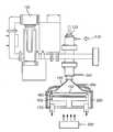
- FIG. 1is a schematic view of a conventional fluorine acid spray apparatus.
- the conventional fluorine acid spray apparatusis comprised of a fluorine acid solution 10 , a heating chamber 20 , a substrate 30 , a substrate mount 40 , a fluorine solution tank 50 filled with a fluorine acid solution 60 , and fluorine acid supply pipes 70 and 80 .
- oxygenis preliminarily removed by forming a fluorine layer on a silicon surface to react with the oxygen.
- a fluorine acid layeris formed on a silicon surface by generating fluorine acid vapor using the fluorine acid spray apparatus and hardened by heat.
- Oxygen introduced into an etching device to etch the fluorine acid layer-having substrate or oxygen remaining in the etching devicereacts chemically with the fluorine acid layer on the surface of the substrate and thus the oxygen is removed.
- UV (UltraViolet) light and ozone (O3)can be used for surface cleaning. That is, a silicon surface is oxidized by reaction between silicon and O3 dissociated by UV light and the oxide layer is removed by wet etch. However, oxidation takes a long time, leading to slow processing.
- FIG. 2is a schematic view of a conventional plasma etching apparatus plasma is generated in a plasma generator 100 by introducing H2 and N2 through a first processing gas inlet 90 and then NF3 is introduced through a second processing gas inlet 110 , thereby etching a silicon substrate 120 in a chamber 140 with gases exhausted through an outlet 130 .
- the NF3 gas as a main processing gasaccelerates plasma dissociation and activation, so that excess fluorine atoms and ions involved in the etching are generated.
- the silicon surfaceis over-etched deeper than a damaged portion, or a BPSG (Borophosphosilicate glass) oxide layer or a nitride layer that must avoid etching may also be etched.
- HSGshemispherical grains
- the surface cleaning apparatus using plasmahas a chamber that can be maintained in a vacuum state, a substrate mount in the chamber, for mounting a silicon substrate, a first processing gas inlet for introducing a carrier gas into the chamber to generate and maintain plasma, a plasma generator for forming plasma out of the first processing gas, a filter between the plasma generator and the substrate mount, for passing only radicals to the substrate, and a second processing gas inlet between the plasma generator and the filter, for introducing a second processing gas into the chamber.
- the plasma generatoruses a microwave generator as an energy source for plasma generation.
- a wall heat jacketis further provided for maintaining the walls of the chamber at a predetermined temperature to concentrate the radicals on the surface of the substrate by preventing deposition of the radicals and formation of a byproduct layer with the radicals.
- the filteris grounded, or a grid or baffle with a square-wave or sine-wave AC (alternating current) voltage applied is used as the filter.
- a third processing gas inletis further provided for introducing a conditioning gas into the chamber to maintain the environment of the chamber constant after processing each wafer.
- a polymer layeris first formed on the oxide layer.
- the polymer layer and the oxide layerare removed by annealing, and the damaged portion of the surface of the silicon substrate is removed.
- plasmais formed by introducing a first processing gas containing H2 or N2, only radicals are passed to the silicon substrate by filtering the plasma, and a second processing gas containing a halogen element is introduced.
- the second processing gasis at least one of HF, HCl, BCl3, HBr, and ClF3.
- the polymer layer and the oxide layerare removed by annealing using a UV lamp or IR lamp, or by annealing in a heat chamber.
- the damaged portion of the silicon substrate surfaceis removed by annealing in a heat chamber.
- the damaged portion removal stepis performed in-situ in the same chamber as the polymer layer and the oxide layer are removed.
- a substrate mountfor mounting a silicon substrate
- a first processing gas inletfor introducing a carrier gas for generation and maintenance of plasma
- a plasma generatorfor passing only radicals to the substrate
- a second processing gas inletthe first processing gas is introduced into the chamber
- plasmais formed out of the first processing gas in the plasma generator
- a second processing gasis introduced into the chamber
- a third processing gasis introduced into the chamber to maintain the environment of the chamber constant after processing each wafer.
- the first processing gascontains one of H2 and N2.
- the filteris grounded or receives an AC voltage.
- the second processing gascontains a halogen element.
- the second processing gasis at least one of HF, HCl, BCl3, HBr, and ClF3.
- the third processing gascontains at least of H, F, O and N.
- FIG. 1is a schematic view of a conventional fluorine acid spray device
- FIG. 2is a schematic view of a conventional plasma etching apparatus
- FIG. 3is a schematic view of an embodiment of plasma etching apparatus according to the present invention.
- FIG. 4is a schematic view of another embodiment of the plasma etching apparatus according to the present invention.
- FIGS. 5A to 5 Eare sectional views sequentially illustrating an embodiment of a process of removing a native oxide layer and a damaged portion of a silicon substrate surface
- FIGS. 6A and 6Bare SEM (Scanning Electro Microscope) images illustrating contact profiles.
- FIG. 3illustrates the structure of an embodiment of plasma etching apparatus according to the present invention.
- the plasma etching apparatusperforms dry cleaning using a microwave plasma.
- a silicon substrate 180is mounted on a substrate mount 160 under a chamber 140 that can be maintained in a vacuum state
- N2, H2, or a mixture of the gasesis introduced through a first processing gas inlet 130 .
- the N2, H2, or mixture gasserves as a carrier gas for generating and maintaining plasma.
- plasmais generated by operating a microwave source module 110 and a plasma applicator 120 and HF gas is introduced through a second processing gas inlet 190 .
- a fluorine-containing halogen element, or a halogen element such as HCl, BCl3, HBr, or ClF3can be a substitute for HF.
- the plasmapasses through a filter 150 , while moving down toward the substrate 180 .
- the filter 150being a grounded baffle or grid, absorbs potential so that only radicals reach the silicon substrate 180 .
- a wall heat jacket 220maintains the walls of the chamber 140 at an appropriate temperature to prevent the radicals from sticking to the walls of the chamber 140 and forming a byproduct layer and to concentrate the radicals on the surface of the silicon substrate 180 .
- H or F gas as a conditioning gasis introduced through a third processing gas inlet 200 to maintain the environment inside the chamber 140 constant and thus increase etch reproducibility after etching.
- the conditioning gasis H, F, O or N, or a mixture of the gases.
- the used processing gasesare exhausted through an outlet 170 .
- FIG. 4illustrates the structure of another embodiment of the plasma etching apparatus according to the present invention.
- the plasma etching apparatusperforms dry cleaning using a remote plasma.
- this plasma etching apparatusis similar to the plasma etching apparatus using a microwave plasma except that RF power is supplied to generate plasma.
- the plasma etching apparatusis well known to those skilled in the field and thus its description is avoided here.
- FIGS. 5A to 5 Eare sectional views sequentially illustrating a process of removing a native oxide layer and a damaged portion of a silicon substrate surface according to an embodiment of the present invention.
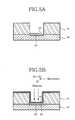
- FIG. 5Aillustrates the step of forming an interlayer insulation layer 41 on a silicon substrate 40 and then forming a contact hole by etching the interlayer insulation layer 41 in a contact area.
- the surface of the silicon substrate 40 exposed in the contact areais damaged during the etching.
- a damaged portion 42 and a native oxide layer 43are sequentially formed on the silicon substrate 40 . Since the native oxide layer 43 and the damaged portion 42 increase contact resistance or leakage current and as a result, deteriorates device characteristics, they must be removed.
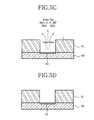
- FIG. 5Billustrates the step of forming an NxHyFz polymer layer 44 or a byproduct on the native oxide layer 43 , the interlayer insulation layer 41 and the sidewalls of a contact hole using plasma generated out of H2 or N2 gas, and HF gas as a second processing gas.
- FIG. 5Cillustrates the step of removing the polymer layer 44 by annealing.
- the decomposed componentare combined with the components of the underlying native oxide layer 43 and excited to N2O, O, F, HT, NH3, SiF4, etc and then removed.
- the polymer layer or byproductcan be removed using a UV lamp or IR (InfraRed) lamp.
- FIG. 5Dillustrates the step of performing hydrophobic cleaning on the silicon substrate surface after the native oxide layer 43 is removed by annealing.
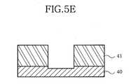
- FIG. 5Eillustrates the step of removing the silicon damaged portion 42 in-situ in the same chamber.
- the silicon damaged portion 42can be removed using a remote plasma of at least one of HF/H2, HF/O2, NF3/O2, SF6/O2, and CF4/O2 or appropriately combining a gas such as NF3, CF4, and C2F2, a gas such as O2, CO2, NO2, and N2, and an inert gas such as He, Ne, Xe, and Ar.
- a remote plasmaincluding Cl, like HCL, ClF3 and so on.
- a table shown belowis a comparison between the present invention using HF as a second processing gas and the conventional technology using NF3 as a second processing gas. As seen from the table, the present invention is much improved in etch rate, silicon substrate roughness, and metal contamination.
- FIG. 6Aillustrates a contact profile before removing a native oxide layer
- FIG. 6Billustrates a contact profile during processing the native oxide layer for 60 seconds. There are little changes in the contact profiles in terms of CD and substrate damage.
Landscapes
- Engineering & Computer Science (AREA)
- Microelectronics & Electronic Packaging (AREA)
- Condensed Matter Physics & Semiconductors (AREA)
- General Physics & Mathematics (AREA)
- Manufacturing & Machinery (AREA)
- Computer Hardware Design (AREA)
- Physics & Mathematics (AREA)
- Power Engineering (AREA)
- Chemical & Material Sciences (AREA)
- Chemical Kinetics & Catalysis (AREA)
- General Chemical & Material Sciences (AREA)
- Inorganic Chemistry (AREA)
- Drying Of Semiconductors (AREA)
- Cleaning Or Drying Semiconductors (AREA)
- Plasma Technology (AREA)
Abstract
Description
- This application claims priority to an application entitled Method of Manufacturing Semiconductor Integrated Circuit and Apparatus Thereof filed in the Korean Industrial Property Office on Jan. 8, 2001 and assigned Serial No. 2001-1018, and to an application entitled Apparatus and Method for Dry Surface Cleaning Using Plasma filed in the Korean Industrial Property Office on Dec. 14, 2001 and assigned Serial No. 2001-79425, the contents of both of which are hereby incorporated by reference.[0001]
- 1. Field of the Invention[0002]
- The present invention relates generally to a surface cleaning apparatus and method using plasma, and in particular, to a surface cleaning apparatus and method for, using plasma, removing a native oxide layer resulting from reaction between oxygen in the air and a silicon surface in fabrication of an integrated circuit such as a semiconductor device or TFT (Thin Film Transistor) LCD (Liquid Crystal Display), an oxide layer chemically formed on the silicon surface during processing, a damaged portion on the silicon surface, or contaminants on the silicon surface and the sidewalls of a contact hole.[0003]
- 2. Description of the Related Art[0004]
- In general, metalization is needed to connect devices formed on an underlying silicon substrate by a metal layer in fabrication of an integrated circuit such as a semiconductor, TFT LCD, or FPD (Flat Panel Display). Formation of a contact hole is requisite for the metalization. The contact hole is formed usually by dry-etching an oxide layer using plasma. In the course of forming the contact hole, the underlying silicon surface is exposed. After the dry etch, a damaged portion is formed due to ion impact from the plasma, and contaminants including materials dissociated from etching gases and etched materials stick to a silicon surface and sidewalls. Because the damaged portion and contaminants may increase contact resistance or leakage current that is deadly adverse to device characteristics, they are removed by dry cleaning or wet cleaning during fabrication of an integrated circuit. Aside from the damaged portion and contaminants, a native oxide layer is formed due to reaction between oxygen in the air and the silicon surface. Therefore, the native oxide layer should also be removed by dry cleaning or wet cleaning before deposition of a conductive material after the contact hole is formed.[0005]
- In addition, an oxide layer can be chemically formed by reaction between the silicon surface and a mixed solution of H2O2, H2SO4, and deionized water used for post-etch processing. The oxide layer influences subsequent steps and deteriorates electrical connection characteristics, thereby degrading the characteristics of a resulting semiconductor or TFT LCD circuit.[0006]
- Along with the decrease of CD(Critical Dimension) in an integrated circuit, a self-aligned contact (SAC) has recently been used widely. During an SAC etch, an etch stopper layer formed of a silicon nitride layer is exposed. Thus, either sidewalls formed of a silicon oxide layer or the nitride layer should not be etched during surface cleaning in order to prevent short between an electrode surrounded by the nitride film and a conductive material filled in a contact hole, or leakage current.[0007]
- Even if the silicon substrate surface underlying the contact hole is not exposed, a gate, a polysilicon electrode for a capacitor, or a connection line can be exposed. In this case, a damaged portion, an oxide layer, or contaminants should be removed as in the case where the silicon substrate surface is exposed.[0008]
- A metal is used for a gate electrode or bit lines of a memory when necessary. The top portion of the metal is exposed during etching a contact hole. Similarly, contaminants on the metal and sidewalls must be removed and much attention should be paid to the removal because etched metal components are contained in the contaminants and are difficult to remove.[0009]
- FIG. 1 is a schematic view of a conventional fluorine acid spray apparatus. Referring to FIG. 1, the conventional fluorine acid spray apparatus is comprised of a[0010]
fluorine acid solution 10, aheating chamber 20, asubstrate 30, asubstrate mount 40, afluorine solution tank 50 filled with afluorine acid solution 60, and fluorineacid supply pipes - Despite the advantage of simplicity in device configuration and concept, however, the above conventional technology has a shortcoming in that it is difficult to effectively control fine process parameters.[0011]
- UV (UltraViolet) light and ozone (O3) can be used for surface cleaning. That is, a silicon surface is oxidized by reaction between silicon and O3 dissociated by UV light and the oxide layer is removed by wet etch. However, oxidation takes a long time, leading to slow processing.[0012]
- FIG. 2 is a schematic view of a conventional plasma etching apparatus plasma is generated in a[0013]
plasma generator 100 by introducing H2 and N2 through a firstprocessing gas inlet 90 and then NF3 is introduced through a secondprocessing gas inlet 110, thereby etching asilicon substrate 120 in achamber 140 with gases exhausted through anoutlet 130. - The NF3 gas as a main processing gas accelerates plasma dissociation and activation, so that excess fluorine atoms and ions involved in the etching are generated. As a result, the silicon surface is over-etched deeper than a damaged portion, or a BPSG (Borophosphosilicate glass) oxide layer or a nitride layer that must avoid etching may also be etched.[0014]
- It is, therefore, an object of the present invention to provide a surface cleaning apparatus and method using plasma, for removing a native oxide layer or a chemical oxide layer formed on a silicon surface before growth of a gate oxide layer in order to prevent deterioration in the characteristics of the gate oxide layer.[0015]
- It is another object of the present invention to provide a surface cleaning apparatus and method using plasma, for removing a native oxide layer/a chemical oxide layer, a damaged portion, and contaminants from a silicon surface exposed during etching a oxide layer for formation of a contact hole in order to prevent the increase of contact resistance and leakage current.[0016]
- It is also another object of the present invention to provide a surface cleaning apparatus and method using plasma, for removing contaminants such as polymers on the sidewalls of a contact hole and the upper surface of an underlying metal layer when the contact hole is etched for connection to the metal layer.[0017]
- It is a further object of the present invention to provide a surface cleaning apparatus and method using plasma, for growing good quality epitaxial silicon by removing a native oxide layer or a chemical oxide layer from a silicon surface during an epitaxial silicon growing process in fabrication of an integrated circuit.[0018]
- It is still another object of the present invention to provide a surface cleaning apparatus and method using plasma, for growing good quality hemispherical grains (HSGs) by removing a native oxide layer or a chemical oxide layer from an underlying silicon surface in an HSG silicon formation process.[0019]
- It is yet another object of the present invention to provide a surface cleaning apparatus and method using plasma, for improving process uniformity.[0020]
- The foregoing and other objects of the present invention can be achieved by providing a surface cleaning apparatus and method using plasma. According to one aspect of the present invention, the surface cleaning apparatus using plasma has a chamber that can be maintained in a vacuum state, a substrate mount in the chamber, for mounting a silicon substrate, a first processing gas inlet for introducing a carrier gas into the chamber to generate and maintain plasma, a plasma generator for forming plasma out of the first processing gas, a filter between the plasma generator and the substrate mount, for passing only radicals to the substrate, and a second processing gas inlet between the plasma generator and the filter, for introducing a second processing gas into the chamber.[0021]
- Preferably, the plasma generator uses a microwave generator as an energy source for plasma generation.[0022]
- Preferably, a wall heat jacket is further provided for maintaining the walls of the chamber at a predetermined temperature to concentrate the radicals on the surface of the substrate by preventing deposition of the radicals and formation of a byproduct layer with the radicals.[0023]
- Preferably, the filter is grounded, or a grid or baffle with a square-wave or sine-wave AC (alternating current) voltage applied is used as the filter.[0024]
- More preferably, a third processing gas inlet is further provided for introducing a conditioning gas into the chamber to maintain the environment of the chamber constant after processing each wafer.[0025]
- According to another aspect of the present invention, in the surface cleaning method using plasma, for removing a damaged portion and an unwanted oxide layer formed during etching for a contact hole on a silicon substrate having at least one layer including an insulation layer, a polymer layer is first formed on the oxide layer. The polymer layer and the oxide layer are removed by annealing, and the damaged portion of the surface of the silicon substrate is removed.[0026]
- Preferably, in the polymer layer formation step, plasma is formed by introducing a first processing gas containing H2 or N2, only radicals are passed to the silicon substrate by filtering the plasma, and a second processing gas containing a halogen element is introduced.[0027]
- Preferably, the second processing gas is at least one of HF, HCl, BCl3, HBr, and ClF3.[0028]
- Preferably, the polymer layer and the oxide layer are removed by annealing using a UV lamp or IR lamp, or by annealing in a heat chamber.[0029]
- Preferably, the damaged portion of the silicon substrate surface is removed by annealing in a heat chamber.[0030]
- More preferably, the damaged portion removal step is performed in-situ in the same chamber as the polymer layer and the oxide layer are removed.[0031]
- According to a further aspect of the present invention, in the surface cleaning method using plasma for fabrication of an integrated circuit in a surface cleaning apparatus having a chamber that can be maintained in a vacuum state, a substrate mount for mounting a silicon substrate, a first processing gas inlet for introducing a carrier gas for generation and maintenance of plasma, a plasma generator, a filter for passing only radicals to the substrate, and a second processing gas inlet, the first processing gas is introduced into the chamber, plasma is formed out of the first processing gas in the plasma generator, a second processing gas is introduced into the chamber, and then a third processing gas is introduced into the chamber to maintain the environment of the chamber constant after processing each wafer.[0032]
- Preferably, the first processing gas contains one of H2 and N2.[0033]
- Preferably, the filter is grounded or receives an AC voltage.[0034]
- Preferably, the second processing gas contains a halogen element.[0035]
- More preferably, the second processing gas is at least one of HF, HCl, BCl3, HBr, and ClF3.[0036]
- Preferably, the third processing gas contains at least of H, F, O and N.[0037]
- The above and other objects, features and advantages of the present invention will become more apparent from the following detailed description when taken in conjunction with the accompanying drawings in which:[0038]
- FIG. 1 is a schematic view of a conventional fluorine acid spray device;[0039]
- FIG. 2 is a schematic view of a conventional plasma etching apparatus;[0040]
- FIG. 3 is a schematic view of an embodiment of plasma etching apparatus according to the present invention;[0041]
- FIG. 4 is a schematic view of another embodiment of the plasma etching apparatus according to the present invention;[0042]
- FIGS. 5A to[0043]5E are sectional views sequentially illustrating an embodiment of a process of removing a native oxide layer and a damaged portion of a silicon substrate surface; and
- FIGS. 6A and 6B are SEM (Scanning Electro Microscope) images illustrating contact profiles.[0044]
- Preferred embodiments of the present invention will be described hereinbelow with reference to the accompanying drawings. In the following description, well-known functions or constructions are not described in detail since they would obscure the invention in unnecessary detail.[0045]
- FIG. 3 illustrates the structure of an embodiment of plasma etching apparatus according to the present invention. The plasma etching apparatus performs dry cleaning using a microwave plasma. Referring to FIG. 3, after a[0046]
silicon substrate 180 is mounted on asubstrate mount 160 under achamber 140 that can be maintained in a vacuum state, N2, H2, or a mixture of the gases is introduced through a firstprocessing gas inlet 130. The N2, H2, or mixture gas serves as a carrier gas for generating and maintaining plasma. Subsequently, plasma is generated by operating amicrowave source module 110 and aplasma applicator 120 and HF gas is introduced through a secondprocessing gas inlet 190. A fluorine-containing halogen element, or a halogen element such as HCl, BCl3, HBr, or ClF3 can be a substitute for HF. The plasma passes through afilter 150, while moving down toward thesubstrate 180. Thefilter 150, being a grounded baffle or grid, absorbs potential so that only radicals reach thesilicon substrate 180. Aheater 210 for annealing, where in the damaged portion of the silicon substrate surface is removed by annealing in a heat chamber. Awall heat jacket 220 maintains the walls of thechamber 140 at an appropriate temperature to prevent the radicals from sticking to the walls of thechamber 140 and forming a byproduct layer and to concentrate the radicals on the surface of thesilicon substrate 180. H or F gas as a conditioning gas is introduced through a thirdprocessing gas inlet 200 to maintain the environment inside thechamber 140 constant and thus increase etch reproducibility after etching. The conditioning gas is H, F, O or N, or a mixture of the gases. - The used processing gases are exhausted through an[0047]
outlet 170. - FIG. 4 illustrates the structure of another embodiment of the plasma etching apparatus according to the present invention. The plasma etching apparatus performs dry cleaning using a remote plasma. Referring to FIG. 4, this plasma etching apparatus is similar to the plasma etching apparatus using a microwave plasma except that RF power is supplied to generate plasma. The plasma etching apparatus is well known to those skilled in the field and thus its description is avoided here.[0048]
- FIGS. 5A to[0049]5E are sectional views sequentially illustrating a process of removing a native oxide layer and a damaged portion of a silicon substrate surface according to an embodiment of the present invention.
- FIG. 5A illustrates the step of forming an[0050]
interlayer insulation layer 41 on asilicon substrate 40 and then forming a contact hole by etching theinterlayer insulation layer 41 in a contact area. The surface of thesilicon substrate 40 exposed in the contact area is damaged during the etching. As a result, a damagedportion 42 and anative oxide layer 43 are sequentially formed on thesilicon substrate 40. Since thenative oxide layer 43 and the damagedportion 42 increase contact resistance or leakage current and as a result, deteriorates device characteristics, they must be removed. - FIG. 5B illustrates the step of forming an[0051]
NxHyFz polymer layer 44 or a byproduct on thenative oxide layer 43, theinterlayer insulation layer 41 and the sidewalls of a contact hole using plasma generated out of H2 or N2 gas, and HF gas as a second processing gas. By grounding a grid or baffle for filtering the plasma, or applying AC voltage, only radicals in the plasma reach the substrate surface. - FIG. 5C illustrates the step of removing the[0052]
polymer layer 44 by annealing. As the components of thepolymer layer 44 are decomposed by annealing, the decomposed component are combined with the components of the underlyingnative oxide layer 43 and excited to N2O, O, F, HT, NH3, SiF4, etc and then removed. Instead of annealing, the polymer layer or byproduct can be removed using a UV lamp or IR (InfraRed) lamp. - FIG. 5D illustrates the step of performing hydrophobic cleaning on the silicon substrate surface after the[0053]
native oxide layer 43 is removed by annealing. - FIG. 5E illustrates the step of removing the silicon damaged[0054]
portion 42 in-situ in the same chamber. The silicon damagedportion 42 can be removed using a remote plasma of at least one of HF/H2, HF/O2, NF3/O2, SF6/O2, and CF4/O2 or appropriately combining a gas such as NF3, CF4, and C2F2, a gas such as O2, CO2, NO2, and N2, and an inert gas such as He, Ne, Xe, and Ar. When removing the silicon damaged portion of a silicon substrate caused during processing including metal etching such as etching for formation of a metal contact window, it is more effective to use a remote plasma including Cl, like HCL, ClF3 and so on. - A table shown below is a comparison between the present invention using HF as a second processing gas and the conventional technology using NF3 as a second processing gas. As seen from the table, the present invention is much improved in etch rate, silicon substrate roughness, and metal contamination.[0055]
Items HF NF3 Reference Etch Rate (/min) 42 30 — Selectivity of Oxide to >8 >6 — Nitride (or Si-sub) SI Surface Roughness 0.2803 0.3623 0.1043 (RMS: nm) Metal Al 7.91E+10 4.38E+12 3.44E+09 Contamination Cr 1.79E+09 5.36E+09 1.79E+09 (/cm3) Fe 3.98E+10 1.43E+11 1.66E+09 Ni 1.60E+09 9.61E+09 1.60E+09 - FIG. 6A illustrates a contact profile before removing a native oxide layer and FIG. 6B illustrates a contact profile during processing the native oxide layer for 60 seconds. There are little changes in the contact profiles in terms of CD and substrate damage.[0056]
- In accordance with the present invention as described above, (1) deterioration of the characteristics of a gate oxide layer is prevented by removing a native oxide layer or a chemical oxide layer formed on a silicon surface before growth of the gate oxide layer; (2) the increase of contact resistance and leakage at a contact are prevented by removing a native oxide layer or a chemical oxide layer formed on a silicon surface exposed after etching for a contact hole and a portion of the silicon surface damaged during etching; (3) metal contact resistance is reduced by removing organic contaminants such as polymers existing at the boundary between the sidewalls of a contact and an underlying metal during etching the metal contact hole; (4) good quality epitaxial silicon is grown by removing a native oxide layer or a chemical oxide layer from a silicon surface in an epitaxial silicon growing process; (5) good quality HSGs are grown by removing a native oxide layer or a chemical oxide layer from a silicon surface in an HSG silicon forming process; and (6) process uniformity is improved by introducing a conditioning gas after processing each wafer and thus maintaining the environment of a chamber constant.[0057]
- While the invention has been shown and described with reference to certain preferred embodiments thereof, it will be understood by those skilled in the art that various changes in form and details may be made therein without departing from the spirit and scope of the invention as defined by the appended claims.[0058]
Claims (26)
1. A surface cleaning method using plasma, for removing a damaged portion and an unwanted oxide layer formed during etching for a contact hole on a silicon substrate having at least one layer including an insulation layer, the method comprising the steps of:
forming a polymer layer on the oxide layer;
removing the polymer layer and the oxide layer by annealing; and
removing the damaged portion of the surface of the silicon substrate.
2. The method ofclaim 1 , the polymer layer formation step comprises the steps of:
forming plasma by introducing a first processing gas containing H2 or N2;
passing only radicals to the silicon substrate by filtering the plasma; and
introducing a second processing gas containing a halogen element.
3. The method ofclaim 2 , wherein the second processing gas is at least one of HF, HCl, BCl3, HBr, and ClF3.
4. The method ofclaim 1 , wherein the polymer layer and the oxide layer are removed by annealing using a UV lamp or IR lamp.
5. The method ofclaim 2 , wherein the polymer layer and the oxide layer are removed by annealing using a UV lamp or IR lamp.
6. The method ofclaim 1 , wherein the polymer layer and the oxide layer are removed by annealing in a heat chamber.
7. The method ofclaim 2 , wherein the polymer layer and the oxide layer are removed by annealing in a heat chamber.
8. The method ofclaim 1 , wherein the damaged portion of the silicon substrate surface is removed using remote plasma formed out of a fluorine (F)-containing gas.
9. The method ofclaim 8 , wherein the fluorine-containing gas is at least one of HF/H2, HF/O2, NF3/O2, SF6/O2, and CF4/O2.
10. The method ofclaim 1 , wherein the damaged portion of the silicon substrate surface is removed using remote plasma formed out of a Cl-containing gas.
11. The method ofclaim 1 , wherein the damaged portion of the silicon substrate surface is removed by annealing in a heat chamber.
12. The method ofclaim 6 , wherein the damaged portion removal step is performed in-situ in the same chamber after removing the polymer layer and the oxide layer.
13. The method ofclaim 7 , wherein the damaged portion removal step is performed in-situ in the same chamber after removing the polymer layer and the oxide layer.
14. A surface cleaning method using plasma for fabrication of an integrated circuit in a surface cleaning apparatus having a chamber that can be maintained in a vacuum state, a substrate mount for mounting a silicon substrate, a first processing gas inlet for introducing a carrier gas for generation and maintenance of plasma, a plasma generator, a filter for passing only radicals to the substrate, and a second processing gas inlet, the method comprising the steps of:
introducing the first processing gas into the chamber;
forming plasma out of the first processing gas in the plasma generator; and
introducing a second processing gas into the chamber.
15. The method ofclaim 14 , wherein the first processing gas contains one of H2 and N2.
16. The method ofclaim 14 , wherein the second processing gas contains a halogen element.
17. The method ofclaim 14 , wherein the second processing gas is at least one of HF, HCl, BCl3, HBr, and ClF3.
18. A surface cleaning method using plasma for fabrication of an integrated circuit in a surface cleaning apparatus having a chamber that can be maintained in a vacuum state, a substrate mount for mounting a silicon substrate, a first processing gas inlet for introducing a carrier gas for generation and maintenance of plasma, a plasma generator, a filter for passing only radicals to the substrate, a second processing gas inlet, and a third processing gas inlet for introducing a third processing gas to maintain the environment of the chamber constant after processing each wafer, the method comprising the steps of:
introducing the first processing gas into the chamber;
forming plasma out of the first processing gas in the plasma generator;
introducing a second processing gas into the chamber; and
introducing the third processing gas into the chamber to maintain the environment of the chamber constant after processing each wafer
19. The method ofclaim 18 , wherein the first processing gas contains one of H2 and N2.
20. The method ofclaim 18 , wherein the second processing gas contains a halogen element.
21. The method ofclaim 18 , wherein the second processing gas is at least one of HF, HCl, BCl3, HBr, and ClF3.
22. The method ofclaim 18 , wherein the third processing gas contains at least of H, F, O and N.
23-31 (cancelled)
32. The method ofclaim 19 , wherein the third processing gas contains at least one of H, F, O and N.
33. The method ofclaim 20 , wherein the third processing gas contains at least one of H, F, O and N.
34. The method ofclaim 21 , wherein the third processing gas contains at least one of H, F, O and N.
Priority Applications (3)
| Application Number | Priority Date | Filing Date | Title |
|---|---|---|---|
| US10/831,252US20040194799A1 (en) | 2001-01-08 | 2004-04-23 | Apparatus and method for surface cleaning using plasma |
| US10/850,261US7111629B2 (en) | 2001-01-08 | 2004-05-20 | Method for cleaning substrate surface |
| US11/385,391US20060157079A1 (en) | 2001-01-08 | 2006-03-21 | Method for cleaning substrate surface |
Applications Claiming Priority (6)
| Application Number | Priority Date | Filing Date | Title |
|---|---|---|---|
| KR2001-1018 | 2001-01-08 | ||
| KR10-2001-0001018AKR100404956B1 (en) | 2001-01-08 | 2001-01-08 | Method of manufacturing semiconductor integrated circuits and apparatus thereof |
| KR2001-79425 | 2001-12-14 | ||
| KR1020010079425AKR100573929B1 (en) | 2001-12-14 | 2001-12-14 | Surface cleaning apparatus and method using plasma |
| US10/038,553US20020124867A1 (en) | 2001-01-08 | 2002-01-04 | Apparatus and method for surface cleaning using plasma |
| US10/831,252US20040194799A1 (en) | 2001-01-08 | 2004-04-23 | Apparatus and method for surface cleaning using plasma |
Related Parent Applications (1)
| Application Number | Title | Priority Date | Filing Date |
|---|---|---|---|
| US10/038,553DivisionUS20020124867A1 (en) | 2001-01-08 | 2002-01-04 | Apparatus and method for surface cleaning using plasma |
Related Child Applications (1)
| Application Number | Title | Priority Date | Filing Date |
|---|---|---|---|
| US10/850,261Continuation-In-PartUS7111629B2 (en) | 2001-01-08 | 2004-05-20 | Method for cleaning substrate surface |
Publications (1)
| Publication Number | Publication Date |
|---|---|
| US20040194799A1true US20040194799A1 (en) | 2004-10-07 |
Family
ID=26638709
Family Applications (2)
| Application Number | Title | Priority Date | Filing Date |
|---|---|---|---|
| US10/038,553AbandonedUS20020124867A1 (en) | 2001-01-08 | 2002-01-04 | Apparatus and method for surface cleaning using plasma |
| US10/831,252AbandonedUS20040194799A1 (en) | 2001-01-08 | 2004-04-23 | Apparatus and method for surface cleaning using plasma |
Family Applications Before (1)
| Application Number | Title | Priority Date | Filing Date |
|---|---|---|---|
| US10/038,553AbandonedUS20020124867A1 (en) | 2001-01-08 | 2002-01-04 | Apparatus and method for surface cleaning using plasma |
Country Status (2)
| Country | Link |
|---|---|
| US (2) | US20020124867A1 (en) |
| JP (1) | JP2002289596A (en) |
Cited By (162)
| Publication number | Priority date | Publication date | Assignee | Title |
|---|---|---|---|---|
| US20070181057A1 (en)* | 2006-02-03 | 2007-08-09 | Applied Materials, Inc. | Epitaxial deposition process and apparatus |
| US20080160210A1 (en)* | 2004-02-26 | 2008-07-03 | Haichun Yang | Passivation layer formation by plasma clean process to reduce native oxide growth |
| US20080190446A1 (en)* | 2007-02-13 | 2008-08-14 | Ranade Rajiv M | Control of dry clean process in wafer processing |
| US20080268645A1 (en)* | 2004-02-26 | 2008-10-30 | Chien-Teh Kao | Method for front end of line fabrication |
| US20090023241A1 (en)* | 2007-07-17 | 2009-01-22 | Gaku Furuta | Clean rate improvement by pressure controlled remote plasma source |
| US20090056746A1 (en)* | 2007-08-29 | 2009-03-05 | Sandhu Gurtej S | Methods For Treating Surfaces, And Apparatuses For Treating Surfaces |
| US20090209107A1 (en)* | 2008-02-14 | 2009-08-20 | Spansion Llc | Method of forming an electronic device including forming features within a mask and a selective removal process |
| US20100221895A1 (en)* | 2007-11-02 | 2010-09-02 | Canon Anelva Corporation | Surface treatment apparatus and surface treatment method |
| US7867900B2 (en) | 2007-09-28 | 2011-01-11 | Applied Materials, Inc. | Aluminum contact integration on cobalt silicide junction |
| US8187970B2 (en) | 2001-07-25 | 2012-05-29 | Applied Materials, Inc. | Process for forming cobalt and cobalt silicide materials in tungsten contact applications |
| US8679982B2 (en) | 2011-08-26 | 2014-03-25 | Applied Materials, Inc. | Selective suppression of dry-etch rate of materials containing both silicon and oxygen |
| US8679983B2 (en) | 2011-09-01 | 2014-03-25 | Applied Materials, Inc. | Selective suppression of dry-etch rate of materials containing both silicon and nitrogen |
| US8765574B2 (en) | 2012-11-09 | 2014-07-01 | Applied Materials, Inc. | Dry etch process |
| US8771539B2 (en) | 2011-02-22 | 2014-07-08 | Applied Materials, Inc. | Remotely-excited fluorine and water vapor etch |
| US8801952B1 (en) | 2013-03-07 | 2014-08-12 | Applied Materials, Inc. | Conformal oxide dry etch |
| US8808563B2 (en) | 2011-10-07 | 2014-08-19 | Applied Materials, Inc. | Selective etch of silicon by way of metastable hydrogen termination |
| US8895449B1 (en) | 2013-05-16 | 2014-11-25 | Applied Materials, Inc. | Delicate dry clean |
| US8921234B2 (en) | 2012-12-21 | 2014-12-30 | Applied Materials, Inc. | Selective titanium nitride etching |
| US8927390B2 (en) | 2011-09-26 | 2015-01-06 | Applied Materials, Inc. | Intrench profile |
| US8951429B1 (en) | 2013-10-29 | 2015-02-10 | Applied Materials, Inc. | Tungsten oxide processing |
| US8956980B1 (en) | 2013-09-16 | 2015-02-17 | Applied Materials, Inc. | Selective etch of silicon nitride |
| US8969212B2 (en) | 2012-11-20 | 2015-03-03 | Applied Materials, Inc. | Dry-etch selectivity |
| US8975152B2 (en) | 2011-11-08 | 2015-03-10 | Applied Materials, Inc. | Methods of reducing substrate dislocation during gapfill processing |
| US8980763B2 (en) | 2012-11-30 | 2015-03-17 | Applied Materials, Inc. | Dry-etch for selective tungsten removal |
| US8999856B2 (en) | 2011-03-14 | 2015-04-07 | Applied Materials, Inc. | Methods for etch of sin films |
| CN104576316A (en)* | 2013-09-16 | 2015-04-29 | Spts技术有限公司 | Pre-cleaning a semiconductor structure |
| US9023732B2 (en) | 2013-03-15 | 2015-05-05 | Applied Materials, Inc. | Processing systems and methods for halide scavenging |
| US9023734B2 (en) | 2012-09-18 | 2015-05-05 | Applied Materials, Inc. | Radical-component oxide etch |
| US9034770B2 (en) | 2012-09-17 | 2015-05-19 | Applied Materials, Inc. | Differential silicon oxide etch |
| US9040422B2 (en) | 2013-03-05 | 2015-05-26 | Applied Materials, Inc. | Selective titanium nitride removal |
| US9064815B2 (en) | 2011-03-14 | 2015-06-23 | Applied Materials, Inc. | Methods for etch of metal and metal-oxide films |
| US9064816B2 (en) | 2012-11-30 | 2015-06-23 | Applied Materials, Inc. | Dry-etch for selective oxidation removal |
| US9111877B2 (en) | 2012-12-18 | 2015-08-18 | Applied Materials, Inc. | Non-local plasma oxide etch |
| US9114438B2 (en) | 2013-05-21 | 2015-08-25 | Applied Materials, Inc. | Copper residue chamber clean |
| US9117855B2 (en) | 2013-12-04 | 2015-08-25 | Applied Materials, Inc. | Polarity control for remote plasma |
| US9132436B2 (en) | 2012-09-21 | 2015-09-15 | Applied Materials, Inc. | Chemical control features in wafer process equipment |
| US9136273B1 (en) | 2014-03-21 | 2015-09-15 | Applied Materials, Inc. | Flash gate air gap |
| US9159606B1 (en) | 2014-07-31 | 2015-10-13 | Applied Materials, Inc. | Metal air gap |
| US9165786B1 (en) | 2014-08-05 | 2015-10-20 | Applied Materials, Inc. | Integrated oxide and nitride recess for better channel contact in 3D architectures |
| US9190293B2 (en) | 2013-12-18 | 2015-11-17 | Applied Materials, Inc. | Even tungsten etch for high aspect ratio trenches |
| US9236266B2 (en) | 2011-08-01 | 2016-01-12 | Applied Materials, Inc. | Dry-etch for silicon-and-carbon-containing films |
| US9236265B2 (en) | 2013-11-04 | 2016-01-12 | Applied Materials, Inc. | Silicon germanium processing |
| US9245762B2 (en) | 2013-12-02 | 2016-01-26 | Applied Materials, Inc. | Procedure for etch rate consistency |
| US9263278B2 (en) | 2013-12-17 | 2016-02-16 | Applied Materials, Inc. | Dopant etch selectivity control |
| US9269590B2 (en) | 2014-04-07 | 2016-02-23 | Applied Materials, Inc. | Spacer formation |
| US9287134B2 (en) | 2014-01-17 | 2016-03-15 | Applied Materials, Inc. | Titanium oxide etch |
| US9287095B2 (en) | 2013-12-17 | 2016-03-15 | Applied Materials, Inc. | Semiconductor system assemblies and methods of operation |
| US9293568B2 (en) | 2014-01-27 | 2016-03-22 | Applied Materials, Inc. | Method of fin patterning |
| US9299537B2 (en) | 2014-03-20 | 2016-03-29 | Applied Materials, Inc. | Radial waveguide systems and methods for post-match control of microwaves |
| US9299575B2 (en) | 2014-03-17 | 2016-03-29 | Applied Materials, Inc. | Gas-phase tungsten etch |
| US9299538B2 (en) | 2014-03-20 | 2016-03-29 | Applied Materials, Inc. | Radial waveguide systems and methods for post-match control of microwaves |
| US9299583B1 (en) | 2014-12-05 | 2016-03-29 | Applied Materials, Inc. | Aluminum oxide selective etch |
| US9309598B2 (en) | 2014-05-28 | 2016-04-12 | Applied Materials, Inc. | Oxide and metal removal |
| US9324576B2 (en) | 2010-05-27 | 2016-04-26 | Applied Materials, Inc. | Selective etch for silicon films |
| US9343272B1 (en) | 2015-01-08 | 2016-05-17 | Applied Materials, Inc. | Self-aligned process |
| US9349605B1 (en) | 2015-08-07 | 2016-05-24 | Applied Materials, Inc. | Oxide etch selectivity systems and methods |
| US9355862B2 (en) | 2014-09-24 | 2016-05-31 | Applied Materials, Inc. | Fluorine-based hardmask removal |
| US9355856B2 (en) | 2014-09-12 | 2016-05-31 | Applied Materials, Inc. | V trench dry etch |
| US9362130B2 (en) | 2013-03-01 | 2016-06-07 | Applied Materials, Inc. | Enhanced etching processes using remote plasma sources |
| US9368364B2 (en) | 2014-09-24 | 2016-06-14 | Applied Materials, Inc. | Silicon etch process with tunable selectivity to SiO2 and other materials |
| US9373522B1 (en) | 2015-01-22 | 2016-06-21 | Applied Mateials, Inc. | Titanium nitride removal |
| US9373517B2 (en) | 2012-08-02 | 2016-06-21 | Applied Materials, Inc. | Semiconductor processing with DC assisted RF power for improved control |
| US9378969B2 (en) | 2014-06-19 | 2016-06-28 | Applied Materials, Inc. | Low temperature gas-phase carbon removal |
| US9378978B2 (en) | 2014-07-31 | 2016-06-28 | Applied Materials, Inc. | Integrated oxide recess and floating gate fin trimming |
| US9385028B2 (en) | 2014-02-03 | 2016-07-05 | Applied Materials, Inc. | Air gap process |
| US9390937B2 (en) | 2012-09-20 | 2016-07-12 | Applied Materials, Inc. | Silicon-carbon-nitride selective etch |
| US9396989B2 (en) | 2014-01-27 | 2016-07-19 | Applied Materials, Inc. | Air gaps between copper lines |
| US9406523B2 (en) | 2014-06-19 | 2016-08-02 | Applied Materials, Inc. | Highly selective doped oxide removal method |
| US9425058B2 (en) | 2014-07-24 | 2016-08-23 | Applied Materials, Inc. | Simplified litho-etch-litho-etch process |
| US9449846B2 (en) | 2015-01-28 | 2016-09-20 | Applied Materials, Inc. | Vertical gate separation |
| US9472417B2 (en) | 2013-11-12 | 2016-10-18 | Applied Materials, Inc. | Plasma-free metal etch |
| US9478432B2 (en) | 2014-09-25 | 2016-10-25 | Applied Materials, Inc. | Silicon oxide selective removal |
| US9493879B2 (en) | 2013-07-12 | 2016-11-15 | Applied Materials, Inc. | Selective sputtering for pattern transfer |
| US9496167B2 (en) | 2014-07-31 | 2016-11-15 | Applied Materials, Inc. | Integrated bit-line airgap formation and gate stack post clean |
| US9502258B2 (en) | 2014-12-23 | 2016-11-22 | Applied Materials, Inc. | Anisotropic gap etch |
| US9499898B2 (en) | 2014-03-03 | 2016-11-22 | Applied Materials, Inc. | Layered thin film heater and method of fabrication |
| US9553102B2 (en) | 2014-08-19 | 2017-01-24 | Applied Materials, Inc. | Tungsten separation |
| US9576809B2 (en) | 2013-11-04 | 2017-02-21 | Applied Materials, Inc. | Etch suppression with germanium |
| US9659753B2 (en) | 2014-08-07 | 2017-05-23 | Applied Materials, Inc. | Grooved insulator to reduce leakage current |
| US9691645B2 (en) | 2015-08-06 | 2017-06-27 | Applied Materials, Inc. | Bolted wafer chuck thermal management systems and methods for wafer processing systems |
| US9721789B1 (en) | 2016-10-04 | 2017-08-01 | Applied Materials, Inc. | Saving ion-damaged spacers |
| US9728437B2 (en) | 2015-02-03 | 2017-08-08 | Applied Materials, Inc. | High temperature chuck for plasma processing systems |
| US9741593B2 (en) | 2015-08-06 | 2017-08-22 | Applied Materials, Inc. | Thermal management systems and methods for wafer processing systems |
| US9768034B1 (en) | 2016-11-11 | 2017-09-19 | Applied Materials, Inc. | Removal methods for high aspect ratio structures |
| US9773648B2 (en) | 2013-08-30 | 2017-09-26 | Applied Materials, Inc. | Dual discharge modes operation for remote plasma |
| US9847289B2 (en) | 2014-05-30 | 2017-12-19 | Applied Materials, Inc. | Protective via cap for improved interconnect performance |
| US9865484B1 (en) | 2016-06-29 | 2018-01-09 | Applied Materials, Inc. | Selective etch using material modification and RF pulsing |
| US9881805B2 (en) | 2015-03-02 | 2018-01-30 | Applied Materials, Inc. | Silicon selective removal |
| US9885117B2 (en) | 2014-03-31 | 2018-02-06 | Applied Materials, Inc. | Conditioned semiconductor system parts |
| US9934942B1 (en) | 2016-10-04 | 2018-04-03 | Applied Materials, Inc. | Chamber with flow-through source |
| US9947549B1 (en) | 2016-10-10 | 2018-04-17 | Applied Materials, Inc. | Cobalt-containing material removal |
| US10026621B2 (en) | 2016-11-14 | 2018-07-17 | Applied Materials, Inc. | SiN spacer profile patterning |
| US10043674B1 (en) | 2017-08-04 | 2018-08-07 | Applied Materials, Inc. | Germanium etching systems and methods |
| US10043684B1 (en) | 2017-02-06 | 2018-08-07 | Applied Materials, Inc. | Self-limiting atomic thermal etching systems and methods |
| US10049891B1 (en) | 2017-05-31 | 2018-08-14 | Applied Materials, Inc. | Selective in situ cobalt residue removal |
| US10062585B2 (en) | 2016-10-04 | 2018-08-28 | Applied Materials, Inc. | Oxygen compatible plasma source |
| US10062579B2 (en) | 2016-10-07 | 2018-08-28 | Applied Materials, Inc. | Selective SiN lateral recess |
| US10062587B2 (en) | 2012-07-18 | 2018-08-28 | Applied Materials, Inc. | Pedestal with multi-zone temperature control and multiple purge capabilities |
| US10062575B2 (en) | 2016-09-09 | 2018-08-28 | Applied Materials, Inc. | Poly directional etch by oxidation |
| CN108682636A (en)* | 2018-05-16 | 2018-10-19 | 汪玉洁 | A kind of wafer etching device |
| US10128086B1 (en) | 2017-10-24 | 2018-11-13 | Applied Materials, Inc. | Silicon pretreatment for nitride removal |
| US10163696B2 (en) | 2016-11-11 | 2018-12-25 | Applied Materials, Inc. | Selective cobalt removal for bottom up gapfill |
| US10170336B1 (en) | 2017-08-04 | 2019-01-01 | Applied Materials, Inc. | Methods for anisotropic control of selective silicon removal |
| US10170282B2 (en) | 2013-03-08 | 2019-01-01 | Applied Materials, Inc. | Insulated semiconductor faceplate designs |
| US10224210B2 (en) | 2014-12-09 | 2019-03-05 | Applied Materials, Inc. | Plasma processing system with direct outlet toroidal plasma source |
| US10242908B2 (en) | 2016-11-14 | 2019-03-26 | Applied Materials, Inc. | Airgap formation with damage-free copper |
| US10256079B2 (en) | 2013-02-08 | 2019-04-09 | Applied Materials, Inc. | Semiconductor processing systems having multiple plasma configurations |
| US10256112B1 (en) | 2017-12-08 | 2019-04-09 | Applied Materials, Inc. | Selective tungsten removal |
| US10283321B2 (en) | 2011-01-18 | 2019-05-07 | Applied Materials, Inc. | Semiconductor processing system and methods using capacitively coupled plasma |
| US10283324B1 (en) | 2017-10-24 | 2019-05-07 | Applied Materials, Inc. | Oxygen treatment for nitride etching |
| US10297458B2 (en) | 2017-08-07 | 2019-05-21 | Applied Materials, Inc. | Process window widening using coated parts in plasma etch processes |
| US10319739B2 (en) | 2017-02-08 | 2019-06-11 | Applied Materials, Inc. | Accommodating imperfectly aligned memory holes |
| US10319600B1 (en) | 2018-03-12 | 2019-06-11 | Applied Materials, Inc. | Thermal silicon etch |
| US10319649B2 (en) | 2017-04-11 | 2019-06-11 | Applied Materials, Inc. | Optical emission spectroscopy (OES) for remote plasma monitoring |
| US10354889B2 (en) | 2017-07-17 | 2019-07-16 | Applied Materials, Inc. | Non-halogen etching of silicon-containing materials |
| US10403507B2 (en) | 2017-02-03 | 2019-09-03 | Applied Materials, Inc. | Shaped etch profile with oxidation |
| US10431429B2 (en) | 2017-02-03 | 2019-10-01 | Applied Materials, Inc. | Systems and methods for radial and azimuthal control of plasma uniformity |
| US10468267B2 (en) | 2017-05-31 | 2019-11-05 | Applied Materials, Inc. | Water-free etching methods |
| US10490418B2 (en) | 2014-10-14 | 2019-11-26 | Applied Materials, Inc. | Systems and methods for internal surface conditioning assessment in plasma processing equipment |
| US10490406B2 (en) | 2018-04-10 | 2019-11-26 | Appled Materials, Inc. | Systems and methods for material breakthrough |
| US10497573B2 (en) | 2018-03-13 | 2019-12-03 | Applied Materials, Inc. | Selective atomic layer etching of semiconductor materials |
| US10504754B2 (en) | 2016-05-19 | 2019-12-10 | Applied Materials, Inc. | Systems and methods for improved semiconductor etching and component protection |
| US10504700B2 (en) | 2015-08-27 | 2019-12-10 | Applied Materials, Inc. | Plasma etching systems and methods with secondary plasma injection |
| US10522371B2 (en) | 2016-05-19 | 2019-12-31 | Applied Materials, Inc. | Systems and methods for improved semiconductor etching and component protection |
| US10541246B2 (en) | 2017-06-26 | 2020-01-21 | Applied Materials, Inc. | 3D flash memory cells which discourage cross-cell electrical tunneling |
| US10541184B2 (en) | 2017-07-11 | 2020-01-21 | Applied Materials, Inc. | Optical emission spectroscopic techniques for monitoring etching |
| US10546729B2 (en) | 2016-10-04 | 2020-01-28 | Applied Materials, Inc. | Dual-channel showerhead with improved profile |
| US10566206B2 (en) | 2016-12-27 | 2020-02-18 | Applied Materials, Inc. | Systems and methods for anisotropic material breakthrough |
| US10573527B2 (en) | 2018-04-06 | 2020-02-25 | Applied Materials, Inc. | Gas-phase selective etching systems and methods |
| US10573496B2 (en) | 2014-12-09 | 2020-02-25 | Applied Materials, Inc. | Direct outlet toroidal plasma source |
| US10593560B2 (en) | 2018-03-01 | 2020-03-17 | Applied Materials, Inc. | Magnetic induction plasma source for semiconductor processes and equipment |
| US10593523B2 (en) | 2014-10-14 | 2020-03-17 | Applied Materials, Inc. | Systems and methods for internal surface conditioning in plasma processing equipment |
| US10615047B2 (en) | 2018-02-28 | 2020-04-07 | Applied Materials, Inc. | Systems and methods to form airgaps |
| US10629473B2 (en) | 2016-09-09 | 2020-04-21 | Applied Materials, Inc. | Footing removal for nitride spacer |
| US10672642B2 (en) | 2018-07-24 | 2020-06-02 | Applied Materials, Inc. | Systems and methods for pedestal configuration |
| US10679870B2 (en) | 2018-02-15 | 2020-06-09 | Applied Materials, Inc. | Semiconductor processing chamber multistage mixing apparatus |
| US10699879B2 (en) | 2018-04-17 | 2020-06-30 | Applied Materials, Inc. | Two piece electrode assembly with gap for plasma control |
| US10727080B2 (en) | 2017-07-07 | 2020-07-28 | Applied Materials, Inc. | Tantalum-containing material removal |
| US10755941B2 (en) | 2018-07-06 | 2020-08-25 | Applied Materials, Inc. | Self-limiting selective etching systems and methods |
| US10854426B2 (en) | 2018-01-08 | 2020-12-01 | Applied Materials, Inc. | Metal recess for semiconductor structures |
| US10872778B2 (en) | 2018-07-06 | 2020-12-22 | Applied Materials, Inc. | Systems and methods utilizing solid-phase etchants |
| US10886137B2 (en) | 2018-04-30 | 2021-01-05 | Applied Materials, Inc. | Selective nitride removal |
| US10892198B2 (en) | 2018-09-14 | 2021-01-12 | Applied Materials, Inc. | Systems and methods for improved performance in semiconductor processing |
| US10903054B2 (en) | 2017-12-19 | 2021-01-26 | Applied Materials, Inc. | Multi-zone gas distribution systems and methods |
| US10920319B2 (en) | 2019-01-11 | 2021-02-16 | Applied Materials, Inc. | Ceramic showerheads with conductive electrodes |
| US10920320B2 (en) | 2017-06-16 | 2021-02-16 | Applied Materials, Inc. | Plasma health determination in semiconductor substrate processing reactors |
| US10943834B2 (en) | 2017-03-13 | 2021-03-09 | Applied Materials, Inc. | Replacement contact process |
| US10964512B2 (en) | 2018-02-15 | 2021-03-30 | Applied Materials, Inc. | Semiconductor processing chamber multistage mixing apparatus and methods |
| US11049755B2 (en) | 2018-09-14 | 2021-06-29 | Applied Materials, Inc. | Semiconductor substrate supports with embedded RF shield |
| US11062887B2 (en) | 2018-09-17 | 2021-07-13 | Applied Materials, Inc. | High temperature RF heater pedestals |
| US11121002B2 (en) | 2018-10-24 | 2021-09-14 | Applied Materials, Inc. | Systems and methods for etching metals and metal derivatives |
| US11257693B2 (en) | 2015-01-09 | 2022-02-22 | Applied Materials, Inc. | Methods and systems to improve pedestal temperature control |
| US11276590B2 (en) | 2017-05-17 | 2022-03-15 | Applied Materials, Inc. | Multi-zone semiconductor substrate supports |
| US11276559B2 (en) | 2017-05-17 | 2022-03-15 | Applied Materials, Inc. | Semiconductor processing chamber for multiple precursor flow |
| US11328909B2 (en) | 2017-12-22 | 2022-05-10 | Applied Materials, Inc. | Chamber conditioning and removal processes |
| US11417534B2 (en) | 2018-09-21 | 2022-08-16 | Applied Materials, Inc. | Selective material removal |
| US11437242B2 (en) | 2018-11-27 | 2022-09-06 | Applied Materials, Inc. | Selective removal of silicon-containing materials |
| US11594428B2 (en) | 2015-02-03 | 2023-02-28 | Applied Materials, Inc. | Low temperature chuck for plasma processing systems |
| US11637002B2 (en) | 2014-11-26 | 2023-04-25 | Applied Materials, Inc. | Methods and systems to enhance process uniformity |
| US11682560B2 (en) | 2018-10-11 | 2023-06-20 | Applied Materials, Inc. | Systems and methods for hafnium-containing film removal |
| US11721527B2 (en) | 2019-01-07 | 2023-08-08 | Applied Materials, Inc. | Processing chamber mixing systems |
| US12340979B2 (en) | 2017-05-17 | 2025-06-24 | Applied Materials, Inc. | Semiconductor processing chamber for improved precursor flow |
Families Citing this family (61)
| Publication number | Priority date | Publication date | Assignee | Title |
|---|---|---|---|---|
| US7111629B2 (en)* | 2001-01-08 | 2006-09-26 | Apl Co., Ltd. | Method for cleaning substrate surface |
| US7497922B2 (en) | 2002-05-08 | 2009-03-03 | Btu International, Inc. | Plasma-assisted gas production |
| US7494904B2 (en) | 2002-05-08 | 2009-02-24 | Btu International, Inc. | Plasma-assisted doping |
| US7432470B2 (en) | 2002-05-08 | 2008-10-07 | Btu International, Inc. | Surface cleaning and sterilization |
| AU2003230265A1 (en) | 2002-05-08 | 2003-11-11 | Dana Corporation | Methods and apparatus for forming and using plasma jets |
| US7498066B2 (en) | 2002-05-08 | 2009-03-03 | Btu International Inc. | Plasma-assisted enhanced coating |
| US7638727B2 (en) | 2002-05-08 | 2009-12-29 | Btu International Inc. | Plasma-assisted heat treatment |
| US7560657B2 (en) | 2002-05-08 | 2009-07-14 | Btu International Inc. | Plasma-assisted processing in a manufacturing line |
| US7445817B2 (en) | 2002-05-08 | 2008-11-04 | Btu International Inc. | Plasma-assisted formation of carbon structures |
| US7465362B2 (en) | 2002-05-08 | 2008-12-16 | Btu International, Inc. | Plasma-assisted nitrogen surface-treatment |
| JP2004022902A (en)* | 2002-06-18 | 2004-01-22 | Fujitsu Ltd | Method for manufacturing semiconductor device |
| US7189940B2 (en)* | 2002-12-04 | 2007-03-13 | Btu International Inc. | Plasma-assisted melting |
| KR101276694B1 (en)* | 2003-02-14 | 2013-06-19 | 어플라이드 머티어리얼스, 인코포레이티드 | Cleaning of native oxide with hydrogen-containing radicals |
| US7232766B2 (en)* | 2003-03-14 | 2007-06-19 | Lam Research Corporation | System and method for surface reduction, passivation, corrosion prevention and activation of copper surface |
| US7078344B2 (en)* | 2003-03-14 | 2006-07-18 | Lam Research Corporation | Stress free etch processing in combination with a dynamic liquid meniscus |
| US7009281B2 (en)* | 2003-03-14 | 2006-03-07 | Lam Corporation | Small volume process chamber with hot inner surfaces |
| US7217649B2 (en)* | 2003-03-14 | 2007-05-15 | Lam Research Corporation | System and method for stress free conductor removal |
| US20040182315A1 (en)* | 2003-03-17 | 2004-09-23 | Tokyo Electron Limited | Reduced maintenance chemical oxide removal (COR) processing system |
| US7173305B2 (en)* | 2003-04-08 | 2007-02-06 | Taiwan Semiconductor Manufacturing Company, Ltd. | Self-aligned contact for silicon-on-insulator devices |
| US8092643B2 (en)* | 2003-06-16 | 2012-01-10 | Ionfield Systems, Llc | Method and apparatus for cleaning and surface conditioning objects using plasma |
| US20060272674A1 (en)* | 2005-06-02 | 2006-12-07 | Cerionx, Inc. | Method and apparatus for cleaning and surface conditioning objects using plasma |
| US8092644B2 (en)* | 2003-06-16 | 2012-01-10 | Ionfield Systems, Llc | Method and apparatus for cleaning and surface conditioning objects using plasma |
| US20060162741A1 (en)* | 2005-01-26 | 2006-07-27 | Cerionx, Inc. | Method and apparatus for cleaning and surface conditioning objects with plasma |
| CA2528194A1 (en)* | 2003-06-16 | 2005-01-06 | Cerionx, Inc. | Atmospheric pressure non-thermal plasma device to clean and sterilize the surface of probes, cannulas, pin tools, pipettes and spray heads |
| US20060272675A1 (en)* | 2005-06-02 | 2006-12-07 | Cerionx, Inc. | Method and apparatus for cleaning and surface conditioning objects using plasma |
| US8366871B2 (en)* | 2003-06-16 | 2013-02-05 | Ionfield Holdings, Llc | Method and apparatus for cleaning and surface conditioning objects using plasma |
| US20060162740A1 (en)* | 2005-01-21 | 2006-07-27 | Cerionx, Inc. | Method and apparatus for cleaning and surface conditioning objects using non-equilibrium atmospheric pressure plasma |
| US6958286B2 (en)* | 2004-01-02 | 2005-10-25 | International Business Machines Corporation | Method of preventing surface roughening during hydrogen prebake of SiGe substrates |
| US20070123051A1 (en)* | 2004-02-26 | 2007-05-31 | Reza Arghavani | Oxide etch with nh4-nf3 chemistry |
| US7030035B2 (en)* | 2004-05-14 | 2006-04-18 | Hitachi Global Storage Technologies Netherlands, B.V. | Prevention of electrostatic wafer sticking in plasma deposition/etch tools |
| US7161247B2 (en)* | 2004-07-28 | 2007-01-09 | Cabot Microelectronics Corporation | Polishing composition for noble metals |
| US7157375B2 (en)* | 2004-08-25 | 2007-01-02 | Agere Systems, Inc. | Methods of downstream microwave photoresist removal and via clean, particularly following Stop-On TiN etching |
| US20070272270A1 (en)* | 2004-12-27 | 2007-11-29 | Kun-Yuan Liao | Single-wafer cleaning procedure |
| WO2006091285A2 (en)* | 2005-01-20 | 2006-08-31 | Cerionx, Inc. | Method and apparatus for cleaning and surface conditioning objects using plasma |
| JP4475136B2 (en)* | 2005-02-18 | 2010-06-09 | 東京エレクトロン株式会社 | Processing system, pre-processing apparatus and storage medium |
| WO2006130779A2 (en)* | 2005-06-02 | 2006-12-07 | Cerionx, Inc. | Method and apparatus for cleaning and surface conditioning objects using plasma |
| US7789965B2 (en) | 2006-09-19 | 2010-09-07 | Asm Japan K.K. | Method of cleaning UV irradiation chamber |
| US20080289650A1 (en)* | 2007-05-24 | 2008-11-27 | Asm America, Inc. | Low-temperature cleaning of native oxide |
| KR101423554B1 (en) | 2007-07-31 | 2014-07-25 | (주)소슬 | Plasma etching apparatus and wafer etching method using the same |
| US7871937B2 (en) | 2008-05-16 | 2011-01-18 | Asm America, Inc. | Process and apparatus for treating wafers |
| EP2200073A4 (en)* | 2008-05-30 | 2012-12-05 | Canon Anelva Corp | PROCESS FOR FORMING SILICIDE AND DEVICE FOR FORMING THE SILICIDE |
| JP2010074065A (en)* | 2008-09-22 | 2010-04-02 | Canon Anelva Corp | Substrate cleaning method for removing oxide film |
| JP5140608B2 (en)* | 2009-01-16 | 2013-02-06 | 株式会社アルバック | Vacuum processing apparatus and vacuum processing method |
| US20100270262A1 (en)* | 2009-04-22 | 2010-10-28 | Applied Materials, Inc. | Etching low-k dielectric or removing resist with a filtered ionized gas |
| KR101041142B1 (en)* | 2009-11-06 | 2011-06-13 | 삼성모바일디스플레이주식회사 | Thin film transistor and its manufacturing method, organic light emitting display device comprising same and manufacturing method thereof |
| CN103443906B (en)* | 2011-03-04 | 2016-03-30 | 应用材料公司 | How to clean the contacts |
| US9396992B2 (en)* | 2014-03-04 | 2016-07-19 | Taiwan Semiconductor Manufacturing Co., Ltd. | Method of using a barrier-seed tool for forming fine-pitched metal interconnects |
| US9299557B2 (en) | 2014-03-19 | 2016-03-29 | Asm Ip Holding B.V. | Plasma pre-clean module and process |
| CN104550133B (en)* | 2014-12-11 | 2017-02-22 | 河北同光晶体有限公司 | Method for removing organic pollutants in hollow micro-defect and on surface of wafer of silicon carbide single crystal |
| US9474163B2 (en) | 2014-12-30 | 2016-10-18 | Asm Ip Holding B.V. | Germanium oxide pre-clean module and process |
| US10373850B2 (en) | 2015-03-11 | 2019-08-06 | Asm Ip Holding B.V. | Pre-clean chamber and process with substrate tray for changing substrate temperature |
| US9761488B2 (en)* | 2015-07-17 | 2017-09-12 | Taiwan Semiconductor Manufacturing Company, Ltd. | Method for cleaning via of interconnect structure of semiconductor device structure |
| US9653310B1 (en)* | 2015-11-11 | 2017-05-16 | Applied Materials, Inc. | Methods for selective etching of a silicon material |
| TWI692799B (en)* | 2015-12-18 | 2020-05-01 | 美商應用材料股份有限公司 | Cleaning method |
| JP6757162B2 (en)* | 2016-03-31 | 2020-09-16 | 芝浦メカトロニクス株式会社 | Plasma processing method and plasma processing equipment |
| KR102363121B1 (en)* | 2018-06-11 | 2022-02-15 | 매슨 테크놀로지 인크 | Generation of hydrogen-reactive species for processing of workpieces |
| US10720337B2 (en)* | 2018-07-20 | 2020-07-21 | Asm Ip Holding B.V. | Pre-cleaning for etching of dielectric materials |
| KR102311907B1 (en)* | 2018-12-26 | 2021-10-14 | 주식회사 테스 | Treatment method for removing an oxide layer of an electrode and etching the electrode |
| JP7030915B2 (en)* | 2020-08-28 | 2022-03-07 | 芝浦メカトロニクス株式会社 | Plasma processing method and plasma processing equipment |
| CN114388350B (en)* | 2022-03-23 | 2022-06-21 | 湖北三维半导体集成创新中心有限责任公司 | Wafer cleaning method and device |
| WO2025090650A1 (en)* | 2023-10-23 | 2025-05-01 | Surfx Technologies Llc | Hydrogen plasma reduction of metal oxide films to metal |
Citations (13)
| Publication number | Priority date | Publication date | Assignee | Title |
|---|---|---|---|---|
| US3923559A (en)* | 1975-01-13 | 1975-12-02 | Bell Telephone Labor Inc | Use of trapped hydrogen for annealing metal-oxide-semiconductor devices |
| US4828369A (en)* | 1986-05-28 | 1989-05-09 | Minolta Camera Kabushiki Kaisha | Electrochromic device |
| US5192717A (en)* | 1989-04-28 | 1993-03-09 | Canon Kabushiki Kaisha | Process for the formation of a polycrystalline semiconductor film by microwave plasma chemical vapor deposition method |
| US5217501A (en)* | 1989-07-25 | 1993-06-08 | Tokyo Electron Limited | Vertical wafer heat treatment apparatus having dual load lock chambers |
| US5284544A (en)* | 1990-02-23 | 1994-02-08 | Hitachi, Ltd. | Apparatus for and method of surface treatment for microelectronic devices |
| US5403434A (en)* | 1994-01-06 | 1995-04-04 | Texas Instruments Incorporated | Low-temperature in-situ dry cleaning process for semiconductor wafer |
| US6055927A (en)* | 1997-01-14 | 2000-05-02 | Applied Komatsu Technology, Inc. | Apparatus and method for white powder reduction in silicon nitride deposition using remote plasma source cleaning technology |
| US6342436B1 (en)* | 1998-01-04 | 2002-01-29 | Sony Corporation | Method of manufacturing semiconductor substrate and method of manufacturing solid-state image-pickup device |
| US6352049B1 (en)* | 1998-02-09 | 2002-03-05 | Applied Materials, Inc. | Plasma assisted processing chamber with separate control of species density |
| US6410991B1 (en)* | 1998-06-15 | 2002-06-25 | Mitsubishi Denki Kabushiki Kaisha | Semiconductor device and method of manufacturing the same |
| US6544900B2 (en)* | 1999-12-23 | 2003-04-08 | Asm America, Inc. | In situ dielectric stacks |
| US6629538B2 (en)* | 2001-01-16 | 2003-10-07 | Hitachi, Ltd. | Method for cleaning semiconductor wafers in a vacuum environment |
| US20050079717A1 (en)* | 1999-10-20 | 2005-04-14 | Savas Stephen E. | Systems and methods for photoresist strip and residue treatment in integrated circuit manufacturing |
- 2002
- 2002-01-04USUS10/038,553patent/US20020124867A1/ennot_activeAbandoned
- 2002-01-07JPJP2002000292Apatent/JP2002289596A/enactivePending
- 2004
- 2004-04-23USUS10/831,252patent/US20040194799A1/ennot_activeAbandoned
Patent Citations (13)
| Publication number | Priority date | Publication date | Assignee | Title |
|---|---|---|---|---|
| US3923559A (en)* | 1975-01-13 | 1975-12-02 | Bell Telephone Labor Inc | Use of trapped hydrogen for annealing metal-oxide-semiconductor devices |
| US4828369A (en)* | 1986-05-28 | 1989-05-09 | Minolta Camera Kabushiki Kaisha | Electrochromic device |
| US5192717A (en)* | 1989-04-28 | 1993-03-09 | Canon Kabushiki Kaisha | Process for the formation of a polycrystalline semiconductor film by microwave plasma chemical vapor deposition method |
| US5217501A (en)* | 1989-07-25 | 1993-06-08 | Tokyo Electron Limited | Vertical wafer heat treatment apparatus having dual load lock chambers |
| US5284544A (en)* | 1990-02-23 | 1994-02-08 | Hitachi, Ltd. | Apparatus for and method of surface treatment for microelectronic devices |
| US5403434A (en)* | 1994-01-06 | 1995-04-04 | Texas Instruments Incorporated | Low-temperature in-situ dry cleaning process for semiconductor wafer |
| US6055927A (en)* | 1997-01-14 | 2000-05-02 | Applied Komatsu Technology, Inc. | Apparatus and method for white powder reduction in silicon nitride deposition using remote plasma source cleaning technology |
| US6342436B1 (en)* | 1998-01-04 | 2002-01-29 | Sony Corporation | Method of manufacturing semiconductor substrate and method of manufacturing solid-state image-pickup device |
| US6352049B1 (en)* | 1998-02-09 | 2002-03-05 | Applied Materials, Inc. | Plasma assisted processing chamber with separate control of species density |
| US6410991B1 (en)* | 1998-06-15 | 2002-06-25 | Mitsubishi Denki Kabushiki Kaisha | Semiconductor device and method of manufacturing the same |
| US20050079717A1 (en)* | 1999-10-20 | 2005-04-14 | Savas Stephen E. | Systems and methods for photoresist strip and residue treatment in integrated circuit manufacturing |
| US6544900B2 (en)* | 1999-12-23 | 2003-04-08 | Asm America, Inc. | In situ dielectric stacks |
| US6629538B2 (en)* | 2001-01-16 | 2003-10-07 | Hitachi, Ltd. | Method for cleaning semiconductor wafers in a vacuum environment |
Cited By (243)
| Publication number | Priority date | Publication date | Assignee | Title |
|---|---|---|---|---|
| US8187970B2 (en) | 2001-07-25 | 2012-05-29 | Applied Materials, Inc. | Process for forming cobalt and cobalt silicide materials in tungsten contact applications |
| US8563424B2 (en) | 2001-07-25 | 2013-10-22 | Applied Materials, Inc. | Process for forming cobalt and cobalt silicide materials in tungsten contact applications |
| US8343307B2 (en) | 2004-02-26 | 2013-01-01 | Applied Materials, Inc. | Showerhead assembly |
| US20080268645A1 (en)* | 2004-02-26 | 2008-10-30 | Chien-Teh Kao | Method for front end of line fabrication |
| US10593539B2 (en) | 2004-02-26 | 2020-03-17 | Applied Materials, Inc. | Support assembly |
| US8846163B2 (en) | 2004-02-26 | 2014-09-30 | Applied Materials, Inc. | Method for removing oxides |
| US20080160210A1 (en)* | 2004-02-26 | 2008-07-03 | Haichun Yang | Passivation layer formation by plasma clean process to reduce native oxide growth |
| US7767024B2 (en) | 2004-02-26 | 2010-08-03 | Appplied Materials, Inc. | Method for front end of line fabrication |
| US7780793B2 (en) | 2004-02-26 | 2010-08-24 | Applied Materials, Inc. | Passivation layer formation by plasma clean process to reduce native oxide growth |
| US7494545B2 (en)* | 2006-02-03 | 2009-02-24 | Applied Materials, Inc. | Epitaxial deposition process and apparatus |
| US20070181057A1 (en)* | 2006-02-03 | 2007-08-09 | Applied Materials, Inc. | Epitaxial deposition process and apparatus |
| US20080190446A1 (en)* | 2007-02-13 | 2008-08-14 | Ranade Rajiv M | Control of dry clean process in wafer processing |
| US20090023241A1 (en)* | 2007-07-17 | 2009-01-22 | Gaku Furuta | Clean rate improvement by pressure controlled remote plasma source |
| US7837805B2 (en) | 2007-08-29 | 2010-11-23 | Micron Technology, Inc. | Methods for treating surfaces |
| US20090056746A1 (en)* | 2007-08-29 | 2009-03-05 | Sandhu Gurtej S | Methods For Treating Surfaces, And Apparatuses For Treating Surfaces |
| US7867900B2 (en) | 2007-09-28 | 2011-01-11 | Applied Materials, Inc. | Aluminum contact integration on cobalt silicide junction |
| US20100255667A1 (en)* | 2007-11-02 | 2010-10-07 | Canon Anelva Corporation | Substrate cleaning method for removing oxide film |
| US20100221895A1 (en)* | 2007-11-02 | 2010-09-02 | Canon Anelva Corporation | Surface treatment apparatus and surface treatment method |
| US10083830B2 (en) | 2007-11-02 | 2018-09-25 | Canon Anelva Corporation | Substrate cleaning method for removing oxide film |
| US20090209107A1 (en)* | 2008-02-14 | 2009-08-20 | Spansion Llc | Method of forming an electronic device including forming features within a mask and a selective removal process |
| US8003545B2 (en)* | 2008-02-14 | 2011-08-23 | Spansion Llc | Method of forming an electronic device including forming features within a mask and a selective removal process |
| US9324576B2 (en) | 2010-05-27 | 2016-04-26 | Applied Materials, Inc. | Selective etch for silicon films |
| US9754800B2 (en) | 2010-05-27 | 2017-09-05 | Applied Materials, Inc. | Selective etch for silicon films |
| US10283321B2 (en) | 2011-01-18 | 2019-05-07 | Applied Materials, Inc. | Semiconductor processing system and methods using capacitively coupled plasma |
| US8771539B2 (en) | 2011-02-22 | 2014-07-08 | Applied Materials, Inc. | Remotely-excited fluorine and water vapor etch |
| US9842744B2 (en) | 2011-03-14 | 2017-12-12 | Applied Materials, Inc. | Methods for etch of SiN films |
| US9064815B2 (en) | 2011-03-14 | 2015-06-23 | Applied Materials, Inc. | Methods for etch of metal and metal-oxide films |
| US10062578B2 (en) | 2011-03-14 | 2018-08-28 | Applied Materials, Inc. | Methods for etch of metal and metal-oxide films |
| US8999856B2 (en) | 2011-03-14 | 2015-04-07 | Applied Materials, Inc. | Methods for etch of sin films |
| US9236266B2 (en) | 2011-08-01 | 2016-01-12 | Applied Materials, Inc. | Dry-etch for silicon-and-carbon-containing films |
| US8679982B2 (en) | 2011-08-26 | 2014-03-25 | Applied Materials, Inc. | Selective suppression of dry-etch rate of materials containing both silicon and oxygen |
| US8679983B2 (en) | 2011-09-01 | 2014-03-25 | Applied Materials, Inc. | Selective suppression of dry-etch rate of materials containing both silicon and nitrogen |
| US8927390B2 (en) | 2011-09-26 | 2015-01-06 | Applied Materials, Inc. | Intrench profile |
| US9012302B2 (en) | 2011-09-26 | 2015-04-21 | Applied Materials, Inc. | Intrench profile |
| US9418858B2 (en) | 2011-10-07 | 2016-08-16 | Applied Materials, Inc. | Selective etch of silicon by way of metastable hydrogen termination |
| US8808563B2 (en) | 2011-10-07 | 2014-08-19 | Applied Materials, Inc. | Selective etch of silicon by way of metastable hydrogen termination |
| US8975152B2 (en) | 2011-11-08 | 2015-03-10 | Applied Materials, Inc. | Methods of reducing substrate dislocation during gapfill processing |
| US10062587B2 (en) | 2012-07-18 | 2018-08-28 | Applied Materials, Inc. | Pedestal with multi-zone temperature control and multiple purge capabilities |
| US10032606B2 (en) | 2012-08-02 | 2018-07-24 | Applied Materials, Inc. | Semiconductor processing with DC assisted RF power for improved control |
| US9373517B2 (en) | 2012-08-02 | 2016-06-21 | Applied Materials, Inc. | Semiconductor processing with DC assisted RF power for improved control |
| US9887096B2 (en) | 2012-09-17 | 2018-02-06 | Applied Materials, Inc. | Differential silicon oxide etch |
| US9034770B2 (en) | 2012-09-17 | 2015-05-19 | Applied Materials, Inc. | Differential silicon oxide etch |
| US9023734B2 (en) | 2012-09-18 | 2015-05-05 | Applied Materials, Inc. | Radical-component oxide etch |
| US9437451B2 (en) | 2012-09-18 | 2016-09-06 | Applied Materials, Inc. | Radical-component oxide etch |
| US9390937B2 (en) | 2012-09-20 | 2016-07-12 | Applied Materials, Inc. | Silicon-carbon-nitride selective etch |
| US9132436B2 (en) | 2012-09-21 | 2015-09-15 | Applied Materials, Inc. | Chemical control features in wafer process equipment |
| US10354843B2 (en) | 2012-09-21 | 2019-07-16 | Applied Materials, Inc. | Chemical control features in wafer process equipment |
| US11264213B2 (en) | 2012-09-21 | 2022-03-01 | Applied Materials, Inc. | Chemical control features in wafer process equipment |
| US9978564B2 (en) | 2012-09-21 | 2018-05-22 | Applied Materials, Inc. | Chemical control features in wafer process equipment |
| US8765574B2 (en) | 2012-11-09 | 2014-07-01 | Applied Materials, Inc. | Dry etch process |
| US8969212B2 (en) | 2012-11-20 | 2015-03-03 | Applied Materials, Inc. | Dry-etch selectivity |
| US9384997B2 (en) | 2012-11-20 | 2016-07-05 | Applied Materials, Inc. | Dry-etch selectivity |
| US9064816B2 (en) | 2012-11-30 | 2015-06-23 | Applied Materials, Inc. | Dry-etch for selective oxidation removal |
| US8980763B2 (en) | 2012-11-30 | 2015-03-17 | Applied Materials, Inc. | Dry-etch for selective tungsten removal |
| US9412608B2 (en) | 2012-11-30 | 2016-08-09 | Applied Materials, Inc. | Dry-etch for selective tungsten removal |
| US9355863B2 (en) | 2012-12-18 | 2016-05-31 | Applied Materials, Inc. | Non-local plasma oxide etch |
| US9111877B2 (en) | 2012-12-18 | 2015-08-18 | Applied Materials, Inc. | Non-local plasma oxide etch |
| US8921234B2 (en) | 2012-12-21 | 2014-12-30 | Applied Materials, Inc. | Selective titanium nitride etching |
| US9449845B2 (en) | 2012-12-21 | 2016-09-20 | Applied Materials, Inc. | Selective titanium nitride etching |
| US11024486B2 (en) | 2013-02-08 | 2021-06-01 | Applied Materials, Inc. | Semiconductor processing systems having multiple plasma configurations |
| US10256079B2 (en) | 2013-02-08 | 2019-04-09 | Applied Materials, Inc. | Semiconductor processing systems having multiple plasma configurations |
| US10424485B2 (en) | 2013-03-01 | 2019-09-24 | Applied Materials, Inc. | Enhanced etching processes using remote plasma sources |
| US9362130B2 (en) | 2013-03-01 | 2016-06-07 | Applied Materials, Inc. | Enhanced etching processes using remote plasma sources |
| US9607856B2 (en) | 2013-03-05 | 2017-03-28 | Applied Materials, Inc. | Selective titanium nitride removal |
| US9040422B2 (en) | 2013-03-05 | 2015-05-26 | Applied Materials, Inc. | Selective titanium nitride removal |
| US8801952B1 (en) | 2013-03-07 | 2014-08-12 | Applied Materials, Inc. | Conformal oxide dry etch |
| US9093390B2 (en) | 2013-03-07 | 2015-07-28 | Applied Materials, Inc. | Conformal oxide dry etch |
| US10170282B2 (en) | 2013-03-08 | 2019-01-01 | Applied Materials, Inc. | Insulated semiconductor faceplate designs |
| US9991134B2 (en) | 2013-03-15 | 2018-06-05 | Applied Materials, Inc. | Processing systems and methods for halide scavenging |
| US9449850B2 (en) | 2013-03-15 | 2016-09-20 | Applied Materials, Inc. | Processing systems and methods for halide scavenging |
| US9184055B2 (en) | 2013-03-15 | 2015-11-10 | Applied Materials, Inc. | Processing systems and methods for halide scavenging |
| US9023732B2 (en) | 2013-03-15 | 2015-05-05 | Applied Materials, Inc. | Processing systems and methods for halide scavenging |
| US9704723B2 (en) | 2013-03-15 | 2017-07-11 | Applied Materials, Inc. | Processing systems and methods for halide scavenging |
| US9153442B2 (en) | 2013-03-15 | 2015-10-06 | Applied Materials, Inc. | Processing systems and methods for halide scavenging |
| US9659792B2 (en) | 2013-03-15 | 2017-05-23 | Applied Materials, Inc. | Processing systems and methods for halide scavenging |
| US9093371B2 (en) | 2013-03-15 | 2015-07-28 | Applied Materials, Inc. | Processing systems and methods for halide scavenging |
| US8895449B1 (en) | 2013-05-16 | 2014-11-25 | Applied Materials, Inc. | Delicate dry clean |
| US9114438B2 (en) | 2013-05-21 | 2015-08-25 | Applied Materials, Inc. | Copper residue chamber clean |
| US9493879B2 (en) | 2013-07-12 | 2016-11-15 | Applied Materials, Inc. | Selective sputtering for pattern transfer |
| US9773648B2 (en) | 2013-08-30 | 2017-09-26 | Applied Materials, Inc. | Dual discharge modes operation for remote plasma |
| US9209012B2 (en) | 2013-09-16 | 2015-12-08 | Applied Materials, Inc. | Selective etch of silicon nitride |
| CN104576316A (en)* | 2013-09-16 | 2015-04-29 | Spts技术有限公司 | Pre-cleaning a semiconductor structure |
| US8956980B1 (en) | 2013-09-16 | 2015-02-17 | Applied Materials, Inc. | Selective etch of silicon nitride |
| US8951429B1 (en) | 2013-10-29 | 2015-02-10 | Applied Materials, Inc. | Tungsten oxide processing |
| US9236265B2 (en) | 2013-11-04 | 2016-01-12 | Applied Materials, Inc. | Silicon germanium processing |
| US9576809B2 (en) | 2013-11-04 | 2017-02-21 | Applied Materials, Inc. | Etch suppression with germanium |
| US9520303B2 (en) | 2013-11-12 | 2016-12-13 | Applied Materials, Inc. | Aluminum selective etch |
| US9711366B2 (en) | 2013-11-12 | 2017-07-18 | Applied Materials, Inc. | Selective etch for metal-containing materials |
| US9472417B2 (en) | 2013-11-12 | 2016-10-18 | Applied Materials, Inc. | Plasma-free metal etch |
| US9245762B2 (en) | 2013-12-02 | 2016-01-26 | Applied Materials, Inc. | Procedure for etch rate consistency |
| US9472412B2 (en) | 2013-12-02 | 2016-10-18 | Applied Materials, Inc. | Procedure for etch rate consistency |
| US9117855B2 (en) | 2013-12-04 | 2015-08-25 | Applied Materials, Inc. | Polarity control for remote plasma |
| US9263278B2 (en) | 2013-12-17 | 2016-02-16 | Applied Materials, Inc. | Dopant etch selectivity control |
| US9287095B2 (en) | 2013-12-17 | 2016-03-15 | Applied Materials, Inc. | Semiconductor system assemblies and methods of operation |
| US9190293B2 (en) | 2013-12-18 | 2015-11-17 | Applied Materials, Inc. | Even tungsten etch for high aspect ratio trenches |
| US9287134B2 (en) | 2014-01-17 | 2016-03-15 | Applied Materials, Inc. | Titanium oxide etch |
| US9396989B2 (en) | 2014-01-27 | 2016-07-19 | Applied Materials, Inc. | Air gaps between copper lines |
| US9293568B2 (en) | 2014-01-27 | 2016-03-22 | Applied Materials, Inc. | Method of fin patterning |
| US9385028B2 (en) | 2014-02-03 | 2016-07-05 | Applied Materials, Inc. | Air gap process |
| US9499898B2 (en) | 2014-03-03 | 2016-11-22 | Applied Materials, Inc. | Layered thin film heater and method of fabrication |
| US9299575B2 (en) | 2014-03-17 | 2016-03-29 | Applied Materials, Inc. | Gas-phase tungsten etch |
| US9837249B2 (en) | 2014-03-20 | 2017-12-05 | Applied Materials, Inc. | Radial waveguide systems and methods for post-match control of microwaves |
| US9299538B2 (en) | 2014-03-20 | 2016-03-29 | Applied Materials, Inc. | Radial waveguide systems and methods for post-match control of microwaves |
| US9564296B2 (en) | 2014-03-20 | 2017-02-07 | Applied Materials, Inc. | Radial waveguide systems and methods for post-match control of microwaves |
| US9299537B2 (en) | 2014-03-20 | 2016-03-29 | Applied Materials, Inc. | Radial waveguide systems and methods for post-match control of microwaves |
| US9136273B1 (en) | 2014-03-21 | 2015-09-15 | Applied Materials, Inc. | Flash gate air gap |
| US9903020B2 (en) | 2014-03-31 | 2018-02-27 | Applied Materials, Inc. | Generation of compact alumina passivation layers on aluminum plasma equipment components |
| US9885117B2 (en) | 2014-03-31 | 2018-02-06 | Applied Materials, Inc. | Conditioned semiconductor system parts |
| US9269590B2 (en) | 2014-04-07 | 2016-02-23 | Applied Materials, Inc. | Spacer formation |
| US9309598B2 (en) | 2014-05-28 | 2016-04-12 | Applied Materials, Inc. | Oxide and metal removal |
| US10465294B2 (en) | 2014-05-28 | 2019-11-05 | Applied Materials, Inc. | Oxide and metal removal |
| US9847289B2 (en) | 2014-05-30 | 2017-12-19 | Applied Materials, Inc. | Protective via cap for improved interconnect performance |
| US9378969B2 (en) | 2014-06-19 | 2016-06-28 | Applied Materials, Inc. | Low temperature gas-phase carbon removal |
| US9406523B2 (en) | 2014-06-19 | 2016-08-02 | Applied Materials, Inc. | Highly selective doped oxide removal method |
| US9425058B2 (en) | 2014-07-24 | 2016-08-23 | Applied Materials, Inc. | Simplified litho-etch-litho-etch process |
| US9773695B2 (en) | 2014-07-31 | 2017-09-26 | Applied Materials, Inc. | Integrated bit-line airgap formation and gate stack post clean |
| US9378978B2 (en) | 2014-07-31 | 2016-06-28 | Applied Materials, Inc. | Integrated oxide recess and floating gate fin trimming |
| US9159606B1 (en) | 2014-07-31 | 2015-10-13 | Applied Materials, Inc. | Metal air gap |
| US9496167B2 (en) | 2014-07-31 | 2016-11-15 | Applied Materials, Inc. | Integrated bit-line airgap formation and gate stack post clean |
| US9165786B1 (en) | 2014-08-05 | 2015-10-20 | Applied Materials, Inc. | Integrated oxide and nitride recess for better channel contact in 3D architectures |
| US9659753B2 (en) | 2014-08-07 | 2017-05-23 | Applied Materials, Inc. | Grooved insulator to reduce leakage current |
| US9553102B2 (en) | 2014-08-19 | 2017-01-24 | Applied Materials, Inc. | Tungsten separation |
| US9355856B2 (en) | 2014-09-12 | 2016-05-31 | Applied Materials, Inc. | V trench dry etch |
| US9368364B2 (en) | 2014-09-24 | 2016-06-14 | Applied Materials, Inc. | Silicon etch process with tunable selectivity to SiO2 and other materials |
| US9355862B2 (en) | 2014-09-24 | 2016-05-31 | Applied Materials, Inc. | Fluorine-based hardmask removal |
| US9478434B2 (en) | 2014-09-24 | 2016-10-25 | Applied Materials, Inc. | Chlorine-based hardmask removal |
| US9613822B2 (en) | 2014-09-25 | 2017-04-04 | Applied Materials, Inc. | Oxide etch selectivity enhancement |
| US9837284B2 (en) | 2014-09-25 | 2017-12-05 | Applied Materials, Inc. | Oxide etch selectivity enhancement |
| US9478432B2 (en) | 2014-09-25 | 2016-10-25 | Applied Materials, Inc. | Silicon oxide selective removal |
| US10490418B2 (en) | 2014-10-14 | 2019-11-26 | Applied Materials, Inc. | Systems and methods for internal surface conditioning assessment in plasma processing equipment |
| US10593523B2 (en) | 2014-10-14 | 2020-03-17 | Applied Materials, Inc. | Systems and methods for internal surface conditioning in plasma processing equipment |
| US10707061B2 (en) | 2014-10-14 | 2020-07-07 | Applied Materials, Inc. | Systems and methods for internal surface conditioning in plasma processing equipment |
| US10796922B2 (en) | 2014-10-14 | 2020-10-06 | Applied Materials, Inc. | Systems and methods for internal surface conditioning assessment in plasma processing equipment |
| US11637002B2 (en) | 2014-11-26 | 2023-04-25 | Applied Materials, Inc. | Methods and systems to enhance process uniformity |
| US9299583B1 (en) | 2014-12-05 | 2016-03-29 | Applied Materials, Inc. | Aluminum oxide selective etch |
| US10224210B2 (en) | 2014-12-09 | 2019-03-05 | Applied Materials, Inc. | Plasma processing system with direct outlet toroidal plasma source |
| US10573496B2 (en) | 2014-12-09 | 2020-02-25 | Applied Materials, Inc. | Direct outlet toroidal plasma source |
| US9502258B2 (en) | 2014-12-23 | 2016-11-22 | Applied Materials, Inc. | Anisotropic gap etch |
| US9343272B1 (en) | 2015-01-08 | 2016-05-17 | Applied Materials, Inc. | Self-aligned process |
| US11257693B2 (en) | 2015-01-09 | 2022-02-22 | Applied Materials, Inc. | Methods and systems to improve pedestal temperature control |
| US9373522B1 (en) | 2015-01-22 | 2016-06-21 | Applied Mateials, Inc. | Titanium nitride removal |
| US9449846B2 (en) | 2015-01-28 | 2016-09-20 | Applied Materials, Inc. | Vertical gate separation |
| US11594428B2 (en) | 2015-02-03 | 2023-02-28 | Applied Materials, Inc. | Low temperature chuck for plasma processing systems |
| US9728437B2 (en) | 2015-02-03 | 2017-08-08 | Applied Materials, Inc. | High temperature chuck for plasma processing systems |
| US10468285B2 (en) | 2015-02-03 | 2019-11-05 | Applied Materials, Inc. | High temperature chuck for plasma processing systems |
| US12009228B2 (en) | 2015-02-03 | 2024-06-11 | Applied Materials, Inc. | Low temperature chuck for plasma processing systems |
| US9881805B2 (en) | 2015-03-02 | 2018-01-30 | Applied Materials, Inc. | Silicon selective removal |
| US9741593B2 (en) | 2015-08-06 | 2017-08-22 | Applied Materials, Inc. | Thermal management systems and methods for wafer processing systems |
| US11158527B2 (en) | 2015-08-06 | 2021-10-26 | Applied Materials, Inc. | Thermal management systems and methods for wafer processing systems |
| US10607867B2 (en) | 2015-08-06 | 2020-03-31 | Applied Materials, Inc. | Bolted wafer chuck thermal management systems and methods for wafer processing systems |
| US9691645B2 (en) | 2015-08-06 | 2017-06-27 | Applied Materials, Inc. | Bolted wafer chuck thermal management systems and methods for wafer processing systems |
| US10147620B2 (en) | 2015-08-06 | 2018-12-04 | Applied Materials, Inc. | Bolted wafer chuck thermal management systems and methods for wafer processing systems |
| US10468276B2 (en) | 2015-08-06 | 2019-11-05 | Applied Materials, Inc. | Thermal management systems and methods for wafer processing systems |
| US9349605B1 (en) | 2015-08-07 | 2016-05-24 | Applied Materials, Inc. | Oxide etch selectivity systems and methods |
| US10424463B2 (en) | 2015-08-07 | 2019-09-24 | Applied Materials, Inc. | Oxide etch selectivity systems and methods |
| US10424464B2 (en) | 2015-08-07 | 2019-09-24 | Applied Materials, Inc. | Oxide etch selectivity systems and methods |
| US10504700B2 (en) | 2015-08-27 | 2019-12-10 | Applied Materials, Inc. | Plasma etching systems and methods with secondary plasma injection |
| US11476093B2 (en) | 2015-08-27 | 2022-10-18 | Applied Materials, Inc. | Plasma etching systems and methods with secondary plasma injection |
| US10522371B2 (en) | 2016-05-19 | 2019-12-31 | Applied Materials, Inc. | Systems and methods for improved semiconductor etching and component protection |
| US10504754B2 (en) | 2016-05-19 | 2019-12-10 | Applied Materials, Inc. | Systems and methods for improved semiconductor etching and component protection |
| US11735441B2 (en) | 2016-05-19 | 2023-08-22 | Applied Materials, Inc. | Systems and methods for improved semiconductor etching and component protection |
| US12057329B2 (en) | 2016-06-29 | 2024-08-06 | Applied Materials, Inc. | Selective etch using material modification and RF pulsing |
| US9865484B1 (en) | 2016-06-29 | 2018-01-09 | Applied Materials, Inc. | Selective etch using material modification and RF pulsing |
| US10062575B2 (en) | 2016-09-09 | 2018-08-28 | Applied Materials, Inc. | Poly directional etch by oxidation |
| US10629473B2 (en) | 2016-09-09 | 2020-04-21 | Applied Materials, Inc. | Footing removal for nitride spacer |
| US10062585B2 (en) | 2016-10-04 | 2018-08-28 | Applied Materials, Inc. | Oxygen compatible plasma source |
| US9721789B1 (en) | 2016-10-04 | 2017-08-01 | Applied Materials, Inc. | Saving ion-damaged spacers |
| US10541113B2 (en) | 2016-10-04 | 2020-01-21 | Applied Materials, Inc. | Chamber with flow-through source |
| US9934942B1 (en) | 2016-10-04 | 2018-04-03 | Applied Materials, Inc. | Chamber with flow-through source |
| US11049698B2 (en) | 2016-10-04 | 2021-06-29 | Applied Materials, Inc. | Dual-channel showerhead with improved profile |
| US10546729B2 (en) | 2016-10-04 | 2020-01-28 | Applied Materials, Inc. | Dual-channel showerhead with improved profile |
| US10224180B2 (en) | 2016-10-04 | 2019-03-05 | Applied Materials, Inc. | Chamber with flow-through source |
| US10319603B2 (en) | 2016-10-07 | 2019-06-11 | Applied Materials, Inc. | Selective SiN lateral recess |
| US10062579B2 (en) | 2016-10-07 | 2018-08-28 | Applied Materials, Inc. | Selective SiN lateral recess |
| US9947549B1 (en) | 2016-10-10 | 2018-04-17 | Applied Materials, Inc. | Cobalt-containing material removal |
| US9768034B1 (en) | 2016-11-11 | 2017-09-19 | Applied Materials, Inc. | Removal methods for high aspect ratio structures |
| US10186428B2 (en) | 2016-11-11 | 2019-01-22 | Applied Materials, Inc. | Removal methods for high aspect ratio structures |
| US10163696B2 (en) | 2016-11-11 | 2018-12-25 | Applied Materials, Inc. | Selective cobalt removal for bottom up gapfill |
| US10770346B2 (en) | 2016-11-11 | 2020-09-08 | Applied Materials, Inc. | Selective cobalt removal for bottom up gapfill |
| US10600639B2 (en) | 2016-11-14 | 2020-03-24 | Applied Materials, Inc. | SiN spacer profile patterning |
| US10242908B2 (en) | 2016-11-14 | 2019-03-26 | Applied Materials, Inc. | Airgap formation with damage-free copper |
| US10026621B2 (en) | 2016-11-14 | 2018-07-17 | Applied Materials, Inc. | SiN spacer profile patterning |
| US10566206B2 (en) | 2016-12-27 | 2020-02-18 | Applied Materials, Inc. | Systems and methods for anisotropic material breakthrough |
| US10403507B2 (en) | 2017-02-03 | 2019-09-03 | Applied Materials, Inc. | Shaped etch profile with oxidation |
| US10431429B2 (en) | 2017-02-03 | 2019-10-01 | Applied Materials, Inc. | Systems and methods for radial and azimuthal control of plasma uniformity |
| US10903052B2 (en) | 2017-02-03 | 2021-01-26 | Applied Materials, Inc. | Systems and methods for radial and azimuthal control of plasma uniformity |
| US10043684B1 (en) | 2017-02-06 | 2018-08-07 | Applied Materials, Inc. | Self-limiting atomic thermal etching systems and methods |
| US10529737B2 (en) | 2017-02-08 | 2020-01-07 | Applied Materials, Inc. | Accommodating imperfectly aligned memory holes |
| US10319739B2 (en) | 2017-02-08 | 2019-06-11 | Applied Materials, Inc. | Accommodating imperfectly aligned memory holes |
| US10325923B2 (en) | 2017-02-08 | 2019-06-18 | Applied Materials, Inc. | Accommodating imperfectly aligned memory holes |
| US10943834B2 (en) | 2017-03-13 | 2021-03-09 | Applied Materials, Inc. | Replacement contact process |
| US10319649B2 (en) | 2017-04-11 | 2019-06-11 | Applied Materials, Inc. | Optical emission spectroscopy (OES) for remote plasma monitoring |
| US11361939B2 (en) | 2017-05-17 | 2022-06-14 | Applied Materials, Inc. | Semiconductor processing chamber for multiple precursor flow |
| US11915950B2 (en) | 2017-05-17 | 2024-02-27 | Applied Materials, Inc. | Multi-zone semiconductor substrate supports |
| US11276590B2 (en) | 2017-05-17 | 2022-03-15 | Applied Materials, Inc. | Multi-zone semiconductor substrate supports |
| US11276559B2 (en) | 2017-05-17 | 2022-03-15 | Applied Materials, Inc. | Semiconductor processing chamber for multiple precursor flow |
| US12340979B2 (en) | 2017-05-17 | 2025-06-24 | Applied Materials, Inc. | Semiconductor processing chamber for improved precursor flow |
| US10049891B1 (en) | 2017-05-31 | 2018-08-14 | Applied Materials, Inc. | Selective in situ cobalt residue removal |
| US10468267B2 (en) | 2017-05-31 | 2019-11-05 | Applied Materials, Inc. | Water-free etching methods |
| US10497579B2 (en) | 2017-05-31 | 2019-12-03 | Applied Materials, Inc. | Water-free etching methods |
| US10920320B2 (en) | 2017-06-16 | 2021-02-16 | Applied Materials, Inc. | Plasma health determination in semiconductor substrate processing reactors |
| US10541246B2 (en) | 2017-06-26 | 2020-01-21 | Applied Materials, Inc. | 3D flash memory cells which discourage cross-cell electrical tunneling |
| US10727080B2 (en) | 2017-07-07 | 2020-07-28 | Applied Materials, Inc. | Tantalum-containing material removal |
| US10541184B2 (en) | 2017-07-11 | 2020-01-21 | Applied Materials, Inc. | Optical emission spectroscopic techniques for monitoring etching |
| US10354889B2 (en) | 2017-07-17 | 2019-07-16 | Applied Materials, Inc. | Non-halogen etching of silicon-containing materials |
| US10593553B2 (en) | 2017-08-04 | 2020-03-17 | Applied Materials, Inc. | Germanium etching systems and methods |
| US10043674B1 (en) | 2017-08-04 | 2018-08-07 | Applied Materials, Inc. | Germanium etching systems and methods |
| US10170336B1 (en) | 2017-08-04 | 2019-01-01 | Applied Materials, Inc. | Methods for anisotropic control of selective silicon removal |
| US10297458B2 (en) | 2017-08-07 | 2019-05-21 | Applied Materials, Inc. | Process window widening using coated parts in plasma etch processes |
| US11101136B2 (en) | 2017-08-07 | 2021-08-24 | Applied Materials, Inc. | Process window widening using coated parts in plasma etch processes |
| US10283324B1 (en) | 2017-10-24 | 2019-05-07 | Applied Materials, Inc. | Oxygen treatment for nitride etching |
| US10128086B1 (en) | 2017-10-24 | 2018-11-13 | Applied Materials, Inc. | Silicon pretreatment for nitride removal |
| US10256112B1 (en) | 2017-12-08 | 2019-04-09 | Applied Materials, Inc. | Selective tungsten removal |
| US10903054B2 (en) | 2017-12-19 | 2021-01-26 | Applied Materials, Inc. | Multi-zone gas distribution systems and methods |
| US12148597B2 (en) | 2017-12-19 | 2024-11-19 | Applied Materials, Inc. | Multi-zone gas distribution systems and methods |
| US11328909B2 (en) | 2017-12-22 | 2022-05-10 | Applied Materials, Inc. | Chamber conditioning and removal processes |
| US10861676B2 (en) | 2018-01-08 | 2020-12-08 | Applied Materials, Inc. | Metal recess for semiconductor structures |
| US10854426B2 (en) | 2018-01-08 | 2020-12-01 | Applied Materials, Inc. | Metal recess for semiconductor structures |
| US10964512B2 (en) | 2018-02-15 | 2021-03-30 | Applied Materials, Inc. | Semiconductor processing chamber multistage mixing apparatus and methods |
| US10679870B2 (en) | 2018-02-15 | 2020-06-09 | Applied Materials, Inc. | Semiconductor processing chamber multistage mixing apparatus |
| US10699921B2 (en) | 2018-02-15 | 2020-06-30 | Applied Materials, Inc. | Semiconductor processing chamber multistage mixing apparatus |
| US10615047B2 (en) | 2018-02-28 | 2020-04-07 | Applied Materials, Inc. | Systems and methods to form airgaps |
| US10593560B2 (en) | 2018-03-01 | 2020-03-17 | Applied Materials, Inc. | Magnetic induction plasma source for semiconductor processes and equipment |
| US11004689B2 (en) | 2018-03-12 | 2021-05-11 | Applied Materials, Inc. | Thermal silicon etch |
| US10319600B1 (en) | 2018-03-12 | 2019-06-11 | Applied Materials, Inc. | Thermal silicon etch |
| US10497573B2 (en) | 2018-03-13 | 2019-12-03 | Applied Materials, Inc. | Selective atomic layer etching of semiconductor materials |
| US10573527B2 (en) | 2018-04-06 | 2020-02-25 | Applied Materials, Inc. | Gas-phase selective etching systems and methods |
| US10490406B2 (en) | 2018-04-10 | 2019-11-26 | Appled Materials, Inc. | Systems and methods for material breakthrough |
| US10699879B2 (en) | 2018-04-17 | 2020-06-30 | Applied Materials, Inc. | Two piece electrode assembly with gap for plasma control |
| US10886137B2 (en) | 2018-04-30 | 2021-01-05 | Applied Materials, Inc. | Selective nitride removal |
| CN108682636A (en)* | 2018-05-16 | 2018-10-19 | 汪玉洁 | A kind of wafer etching device |
| US10872778B2 (en) | 2018-07-06 | 2020-12-22 | Applied Materials, Inc. | Systems and methods utilizing solid-phase etchants |
| US10755941B2 (en) | 2018-07-06 | 2020-08-25 | Applied Materials, Inc. | Self-limiting selective etching systems and methods |
| US10672642B2 (en) | 2018-07-24 | 2020-06-02 | Applied Materials, Inc. | Systems and methods for pedestal configuration |
| US11049755B2 (en) | 2018-09-14 | 2021-06-29 | Applied Materials, Inc. | Semiconductor substrate supports with embedded RF shield |
| US10892198B2 (en) | 2018-09-14 | 2021-01-12 | Applied Materials, Inc. | Systems and methods for improved performance in semiconductor processing |
| US11062887B2 (en) | 2018-09-17 | 2021-07-13 | Applied Materials, Inc. | High temperature RF heater pedestals |
| US11417534B2 (en) | 2018-09-21 | 2022-08-16 | Applied Materials, Inc. | Selective material removal |
| US11682560B2 (en) | 2018-10-11 | 2023-06-20 | Applied Materials, Inc. | Systems and methods for hafnium-containing film removal |
| US11121002B2 (en) | 2018-10-24 | 2021-09-14 | Applied Materials, Inc. | Systems and methods for etching metals and metal derivatives |
| US11437242B2 (en) | 2018-11-27 | 2022-09-06 | Applied Materials, Inc. | Selective removal of silicon-containing materials |
| US11721527B2 (en) | 2019-01-07 | 2023-08-08 | Applied Materials, Inc. | Processing chamber mixing systems |
| US10920319B2 (en) | 2019-01-11 | 2021-02-16 | Applied Materials, Inc. | Ceramic showerheads with conductive electrodes |
Also Published As
| Publication number | Publication date |
|---|---|
| JP2002289596A (en) | 2002-10-04 |
| US20020124867A1 (en) | 2002-09-12 |
Similar Documents
| Publication | Publication Date | Title |
|---|---|---|
| US20040194799A1 (en) | Apparatus and method for surface cleaning using plasma | |
| US7111629B2 (en) | Method for cleaning substrate surface | |
| US6692903B2 (en) | Substrate cleaning apparatus and method | |
| US6380095B1 (en) | Silicon trench etch using silicon-containing precursors to reduce or avoid mask erosion | |
| US6440864B1 (en) | Substrate cleaning process | |
| US6638855B1 (en) | Method of filling contact hole of semiconductor device | |
| EP0801606B1 (en) | Method for treating a surface | |
| KR100316721B1 (en) | Method of manufacturing semiconductor device having a silicide layer | |
| US8716143B1 (en) | Plasma based photoresist removal system for cleaning post ash residue | |
| US20060252265A1 (en) | Etching high-kappa dielectric materials with good high-kappa foot control and silicon recess control | |
| EP0651434A2 (en) | Oxide etch process with high selectivity to nitride suitable for use on surfaces of uneven topography | |
| US20090176375A1 (en) | Method of Etching a High Aspect Ratio Contact | |
| TWI658508B (en) | Plasma treatment method | |
| KR100360399B1 (en) | Method of manufacturing semiconductor capacitor having a hemispherical grain layer | |
| US6303513B1 (en) | Method for controlling a profile of a structure formed on a substrate | |
| US6194325B1 (en) | Oxide etch process with high selectivity to nitride suitable for use on surfaces of uneven topography | |
| KR100573929B1 (en) | Surface cleaning apparatus and method using plasma | |
| KR100404956B1 (en) | Method of manufacturing semiconductor integrated circuits and apparatus thereof | |
| KR20030049086A (en) | System and method for dry cleaning of substrate | |
| KR100271763B1 (en) | Apparatus and method for etching polysilicon layer | |
| KR101333831B1 (en) | Surface processing method of semiconductor device and surface processing method thereof | |
| TWI892833B (en) | Systems and methods for selective metal-containing hardmask removal | |
| Ooka et al. | Contact-hole etching with NH3-added C5F8 pulse-modulated plasma | |
| TW202503844A (en) | Systems and methods for titanium-containing film removal | |
| JPH0888223A (en) | Method for manufacturing semiconductor device |
Legal Events
| Date | Code | Title | Description |
|---|---|---|---|
| STCB | Information on status: application discontinuation | Free format text:ABANDONED -- FAILURE TO RESPOND TO AN OFFICE ACTION |