US20040189585A1 - Shift register and display device having the same - Google Patents
Shift register and display device having the sameDownload PDFInfo
- Publication number
- US20040189585A1 US20040189585A1US10/783,252US78325204AUS2004189585A1US 20040189585 A1US20040189585 A1US 20040189585A1US 78325204 AUS78325204 AUS 78325204AUS 2004189585 A1US2004189585 A1US 2004189585A1
- Authority
- US
- United States
- Prior art keywords
- transistor
- clock signal
- pull
- driving part
- signal
- Prior art date
- Legal status (The legal status is an assumption and is not a legal conclusion. Google has not performed a legal analysis and makes no representation as to the accuracy of the status listed.)
- Granted
Links
Images


Classifications
- G—PHYSICS
- G11—INFORMATION STORAGE
- G11C—STATIC STORES
- G11C19/00—Digital stores in which the information is moved stepwise, e.g. shift registers
- G11C19/18—Digital stores in which the information is moved stepwise, e.g. shift registers using capacitors as main elements of the stages
- G11C19/182—Digital stores in which the information is moved stepwise, e.g. shift registers using capacitors as main elements of the stages in combination with semiconductor elements, e.g. bipolar transistors, diodes
- G11C19/184—Digital stores in which the information is moved stepwise, e.g. shift registers using capacitors as main elements of the stages in combination with semiconductor elements, e.g. bipolar transistors, diodes with field-effect transistors, e.g. MOS-FET
- G—PHYSICS
- G11—INFORMATION STORAGE
- G11C—STATIC STORES
- G11C19/00—Digital stores in which the information is moved stepwise, e.g. shift registers
- G11C19/28—Digital stores in which the information is moved stepwise, e.g. shift registers using semiconductor elements
- G—PHYSICS
- G09—EDUCATION; CRYPTOGRAPHY; DISPLAY; ADVERTISING; SEALS
- G09G—ARRANGEMENTS OR CIRCUITS FOR CONTROL OF INDICATING DEVICES USING STATIC MEANS TO PRESENT VARIABLE INFORMATION
- G09G3/00—Control arrangements or circuits, of interest only in connection with visual indicators other than cathode-ray tubes
- G09G3/20—Control arrangements or circuits, of interest only in connection with visual indicators other than cathode-ray tubes for presentation of an assembly of a number of characters, e.g. a page, by composing the assembly by combination of individual elements arranged in a matrix no fixed position being assigned to or needed to be assigned to the individual characters or partial characters
- G09G3/34—Control arrangements or circuits, of interest only in connection with visual indicators other than cathode-ray tubes for presentation of an assembly of a number of characters, e.g. a page, by composing the assembly by combination of individual elements arranged in a matrix no fixed position being assigned to or needed to be assigned to the individual characters or partial characters by control of light from an independent source
- G09G3/36—Control arrangements or circuits, of interest only in connection with visual indicators other than cathode-ray tubes for presentation of an assembly of a number of characters, e.g. a page, by composing the assembly by combination of individual elements arranged in a matrix no fixed position being assigned to or needed to be assigned to the individual characters or partial characters by control of light from an independent source using liquid crystals
- G09G3/3611—Control of matrices with row and column drivers
- G09G3/3674—Details of drivers for scan electrodes
- G09G3/3677—Details of drivers for scan electrodes suitable for active matrices only
Definitions
- the present inventionrelates to a gate driver generating scan signals in a display device, and more particularly to a shift register in a gate driver, which operates with a reduced number of external bus lines, and a display device employing such a shift register.
- Image display devicessuch as liquid crystal display devices, are generally equipped with a gate driver using a tape carrier package (TCP), a chip on glass (COG), etc.
- TCPtape carrier package
- COGchip on glass
- a display devicehas a gate driving part which is not installed in the form of an IC on a display panel but is integrally formed at a portion of a display panel.
- the structure of such gate driving partis called “gate-IC-less structure” in this description.
- amorphous silicon thin film transistorsa-Si TFTs
- Examples of a-Si TFTcan be found in U.S. Pat. No. 5,517,542 and commonly assigned Korean Patent Application No. 2002-3398 (or Korean Laid Open Publication No. 2002-66962).
- the conventional gate driving part with the gate-IC-less structureincludes one or more shift registers to provide scan signals to a display panel.
- FIG. 1is a circuit diagram illustrating a unit stage of a conventional shift register.
- the stage 100 of a conventional shift registerincludes a pull-up part 110 , a pull-down part 120 , a pull-up driving part 130 , and a pull-down driving part 140 .
- the stage 100generates a gate signal (or scan signal) in response to a scan start signal STV or an output signal of a previous stage.
- the stage 100receives the scan start signal STV to output the gate signal.
- the stage 100receives a gate signal generated from a previous stage to output the gate signal.
- a shift register having such stage(s)is mounted on a TFT panel of a display device.
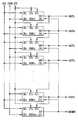
- FIG. 2is a block diagram illustrating a conventional shift register including multiple stages as shown in FIG. 1.
- the shift register 174has ‘N’ stages SRC 1 -SRC N for generating ‘N’ gate signals (or scan signals) GOUT 1 -GOUT N , respectively, and a dummy stage SRC N+1 for providing a control signal to the previous stage.
- the stages SRC 1 -SRC Neach receive first and second clock signals CKV, CKVB, high and ground level voltages VDD, VSS as gate turn-on and -off voltages VON, VOFF, and a control signal from an output of the next stage.
- the first stagereceives a scan start signal STV in addition to the above mentioned signals to output the first gate signal GOUT 1 for selecting the first gate line.
- the first gate signal GOUT 1is also provided to an input terminal IN of the second stage.
- the second stage SRC 2receives the first gate signal GOUT 1 from the first stage in addition to the above mentioned signals to output the second gate signal GOUT 2 for selecting the second gate line.
- the second gate signal GOUT 2is also provided to an input terminal IN of the third stage SRC 3 .
- the N-th stage SRC Nreceives the (N ⁇ 1)-th gate signal from an (N ⁇ 1)-th stage and a control signal from the dummy stage SRC N+1 in addition to the other clock and voltage signals to output the N-th gate signal GOUT N for selecting N-th gate line.
- FIG. 3is a graphical view of signal waveforms of the shift register in FIG. 1.
- a stage in the shift register 174receives the first or second clock signal CKV/CKVB, that is, the odd numbered ones of the stages receive the first clock signal CKV, and the even numbered ones receive the second clock signal CKVB that has an inverted phase with respect to the first clock signal CKV.
- the shift register 174generates the gate signals to the gate lines of a TFT substrate in sequence.
- the first and second clock signals CKV, CKVBare obtained from an output signal of a timing controller (not shown).
- the output signal of the timing controllerhas an amplitude in the range from 0V to 3V and is amplified to be in the range from ⁇ 8V to 24V to drive a-Si TFT.
- the first and second clock signalsuse the amplified output signal.
- a conventional shift register having the gate-IC-less structure with a-Si transistorrequires at least five bus lines: a bus line for transferring the scan start signal STV that is a start signal in a horizontal direction, a bus line for transferring the first clock signal CKV to apply the gate off voltage, which is connected to odd numbered gate lines, a bus line for transferring the second clock signal CKVB to apply the gate off voltage, which is connected to even numbered gate lines, and bus lines for providing the high and ground level voltages VDD, VSS to each of the stages.
- the five bus linesare connected to a gate driver region of a display panel via a dummy pin of TCP having source driver IC mounted thereon, or the five bus lines are attached on the display panel to be connected to the gate driver region.
- the conventional shift registershave problems including the followings.
- a separate space for forming a jumper that transfers signals and power to each of the stagesis required.
- the space for the bus linesis more limited.
- the five or more bus linesare formed via TCP or FPC, a dummy space of the TCP and a width of the FPC are increased so that the manufacturing cost increases and the space for the bus lines is more limited.
- the a-Si transistorwhen the a-Si transistor is used for a gate driver circuit, the a-Si transistor may be damaged in DC bias state such as the gate on and off voltages VON, VOFF. As a result, the a-Si transistor malfunctions.
- the a-Si transistorneeds a large voltage difference such as ⁇ 14V to 20V, so that metal pads of the display panel may be damaged due to the large voltage difference.
- the metal padsmay be eroded or undesirable electric paths may be formed between the metal pads due to the humidity.
- a shift register for providing gate signals to corresponding gate lines in a display deviceincludes a plurality of stages respectively generating the gate signals in sequence, in which each of the stages includes a first pull-up driving part to generate a first control signal in response to an output signal of an adjacent previous stage or a control signal, a pull-up part to generate a current output signal in response to a first clock signal and the first control signal, a second pull-up driving part to generate at least one second control signal in response to the first clock signal and a second clock signal, and a third pull-up driving part connected to a low level terminal to operate in response to an output signal of an adjacent following stage.
- the stagealso includes a pull-down part to operate in response to the second clock signal.
- the shift registermay be integrally formed with the display panel at a selected region of the display panel.
- the second pull-up driving partmay include a first transistor having a gate electrode receiving the gate signal and a conduction path connected between a terminal receiving the first clock signal and a terminal receiving the second clock signal, a second transistor connected between the terminal receiving the first clock signal and the first transistor, the second transistor operating as a diode, and a third transistor having a gate electrode receiving the second clock signal and a conduction path connected between the terminal receiving the first clock signal and the common node of the first and second transistors of the second pull-up driving part, in which the common node is connected to the third pull-up driving part.
- the third pull-up driving partincludes a first transistor having two terminals connected to the first control signal, a second transistor having a gate electrode connected to the common node of the second pull-up driving part and a conduction path connected between the first transistor and the second clock signal, a third transistor having a gate electrode connected to the output signal of the adjacent following stage and a conduction path connected between the pull-up part and the low level terminal, and a capacitor connected between the pull-up part and the current output signal.
- the second pull-up driving partmay include a first transistor having a gate electrode receiving the gate signal and a conduction path connected between a terminal receiving the first clock signal and a terminal receiving the second clock signal, a second transistor having a gate electrode receiving a second transistor control signal and a conduction path connected between the terminal receiving the first clock signal and the first transistor of the second pull-up driving part, in which a common node of the first and second transistors of the second pull-up driving part is connected to the gate electrode of the hold transistor of the first pull-up driving part, a third transistor having a gate electrode receiving the second clock signal and a conduction path connected between the terminal receiving the first clock signal and the common node of the first and second transistors of the second pull-up driving part, a fourth transistor having a gate electrode receiving the gate signal and a conduction path connected between the terminal receiving the first clock signal and the terminal receiving the second clock signal, a fifth transistor connected between the terminal receiving the first clock signal and the fourth transistor of the control member, in which the fifth transistor
- the second pull-up driving partmay include a first transistor having a gate electrode receiving the gate signal and a conduction path connected between a terminal receiving the first clock signal and a terminal receiving the second clock signal, a second transistor having a gate electrode receiving a second transistor control signal and a conduction path connected between the terminal receiving the first clock signal and the first transistor of the second pull-up driving part, in which a common node of the first and second transistors of the second pull-up driving part is connected to the gate electrode of the hold transistor of the first pull-up driving part, a third transistor having a gate electrode receiving the second clock signal and a conduction path connected between the terminal receiving the first clock signal and the common node of the first and second transistors of the second pull-up driving part, a fourth transistor having a gate electrode receiving the gate signal and a conduction path connected between the terminal receiving the first clock signal and the terminal receiving the second clock signal, a fifth transistor connected between the terminal receiving the first clock signal and the fourth transistor of the control member, in which the fifth transistor
- the second pull-up driving partmay include a first transistor having a gate electrode receiving the gate signal and a conduction path connected between a terminal receiving the first clock signal and a terminal receiving the second clock signal, a second transistor having a gate electrode receiving a second transistor control signal and a conduction path connected between the terminal receiving the first clock signal and the first transistor of the second pull-up driving part, in which a common node of the first and second transistors of the second pull-up driving part is connected to the gate electrode of the hold transistor of the first pull-up driving part, a third transistor having a gate electrode receiving the second clock signal and a conduction path connected between the terminal receiving the first clock signal and the common node of the first and second transistors of the second pull-up driving part, a fourth transistor having a gate electrode receiving the gate signal and a conduction path connected between the terminal receiving the first clock signal and the terminal receiving the second clock signal, a fifth transistor connected between the terminal receiving the first clock signal and the fourth transistor of the control member, in which the fifth
- FIG. 1is a circuit diagram illustrating a unit stage of a conventional shift register
- FIG. 2is a block diagram illustrating a conventional shift register
- FIG. 3is a graphical view of signal waveforms of the shift register in FIG. 1;
- FIG. 4is a block diagram illustrating a shift register according to an exemplary embodiment of the present invention.
- FIG. 5is a circuit diagram illustrating a unit stage of the shift register in FIG. 4;
- FIG. 6is a circuit diagram illustrating the shift register in FIG. 4;
- FIG. 7is a circuit diagram illustrating a unit stage of a shift register according to another exemplary embodiment of the present invention.
- FIG. 8is a circuit diagram illustrating a shift register including the unit stage in FIG.7;
- FIG. 9is a circuit diagram illustrating a unit stage of a shift register according to another exemplary embodiment of the present invention.
- FIG. 10is a circuit diagram illustrating a shift register including the unit stage in FIG. 9;
- FIG. 11is a circuit diagram illustrating a unit stage of a shift register according to another exemplary embodiment of the present invention.
- FIG. 12is a circuit diagram illustrating a shift register including the unit stage in FIG. 11;
- FIG. 13is a circuit diagram illustrating a unit stage of a shift register according to another exemplary embodiment of the present invention.
- FIG. 14is a circuit diagram illustrating a shift register including the unit stage in FIG. 13;
- FIG. 15is a circuit diagram illustrating a unit stage of a shift register according to another exemplary embodiment of the present invention.
- FIG. 16is a circuit diagram illustrating a shift register including the unit stage in FIG. 15;
- FIG. 17is a circuit diagram illustrating a unit stage of a shift register according to another exemplary embodiment of the present invention.
- FIG. 18is a circuit diagram illustrating a shift register including the unit stage in FIG. 17.
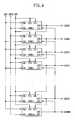
- FIG. 4is a block diagram illustrating a shift register according to an exemplary embodiment of the present invention.
- the shift registerincludes ‘N’ stages ASRC 1 -ASRC N for generating gate signals (or scan signals) GOUT 1 -GOUT N , respectively, and a dummy stage ASRC N+1 for generating a dummy gate signal GDUMMY that is provided to the previous stage ASRC N as a control signal.
- the shift registeris formed on the same plane as a display panel (e.g., a liquid crystal display panel) is formed.
- the display planehas switching devices formed at a region defined by gate lines (or scan lines) and data lines.
- the shift registeroutputs the gate signals GOUT 1 -GOUT N each of which is provided to corresponding one of the switching devices as a scan signal.
- the stages ASRC 1 -ASRC Neach have first and second clock terminals CK 1 , CK 2 for receiving first and second clock signals CKV, CKVB externally provided.
- the first and second clock signals CKV, CKVeach have a phase inverted with respect to each other.
- the respective stages ASRC 1 -ASRC Nalso have first to third control signals CT 1 -CT 3 for receiving corresponding control signals and an output terminal OUT generating the respective gate signals GOUT 1 -GOUT N .
- the first stage ASRC 1receives the first and second clock signals CKV, CKVB via the first and second clock terminals CK 1 , CK 2 , respectively.
- the first stage ASRC 1also receives a scan start signal STV via the first and third control terminals CT 1 , CT 3 and a second gate signal GOUT 2 generated from the next stage ASRC 2 via the second control terminal CT 2 .
- the first stage ASRC 1outputs a first gate signal GOUT 1 for selecting the first gate line.
- the first gate signal GOUT 1is also provided to the first control terminal CT 1 of the second stage ASRC 2 .
- the second stage ASRC 2receives the first and second clock signals CKV, CKVB via the second and first clock terminals CK 2 , CK 1 , respectively.
- the second stage ASRC 2receives the first gate signal GOUT 1 generated from the first stage ASRC 1 via the first control terminal CT 1 and a third gate signal GOUT 3 generated from a third stage ASRC 3 via the second control terminal CT 2 .
- the second stage ASRC 2also receives the scan start signal STV via the third control terminal CT 3 . Then, the second stage ASRC 2 outputs the second gate signal GOUT 2 for selecting the second gate line.
- the second gate signal GOUT 2is provided to the first control terminal CT 1 of the third stage ASRC 3 .
- the N-th stage ASRC Nreceives the first and second clock signals CKV, CKVB via the second and first clock terminals CK 2 , CK 1 , respectively.
- the N-th stage ASRC Nreceives the dummy gate signal GDUMMY generated from the dummy stage ASRC N+1 via the second control terminal CT 2 .
- the N-th stage ASRC Nalso receives the scan start signal STV via the third control terminal CT 3 .
- the N-th stage ASRC Noutputs the N-th gate signal GOUT N for selecting the N-th gate line.
- the N-th gate signal GOUT Nis also provided to a first control terminal CT 1 of the dummy stage ASRC N+1 .
- the shift registerrequires only three bus lines for receiving the scan start signal STV and the first and second clock signals CK, CKVB to output the gate signals GOUT 1 -GOUT N for selecting gate lines. In other words, the shift register does not necessitate the bus lines for receiving ground level and high level voltages that are required in the conventional shift registers.
- FIG. 5is a circuit diagram illustrating a unit stage of the shift register in FIG. 4, and FIG. 6 is a circuit diagram illustrating a shift register having the unit stage of FIG. 5.
- the stage 200 of the shift registerincludes a pull-up part 210 , a pull-down part 220 , and first, second, third second pull-up driving parts 230 , 250 , 240 .
- the stage 200outputs a gate signal (or scan signal) by using the scan start signal STV and the output signals of the previous and next stages.
- the pull-up part 210includes a first NMOS transistor M 1 having a drain electrode (or a second current electrode) electrically connected to a first clock signal terminal CK 1 , a source electrode (or a first current electrode) electrically connected to an output terminal GOUT.
- the pull-up part 210outputs the gate signal GOUT[N].
- the pull-down part 220includes second and third NMOS transistors M 2 , M 3 .
- the second NMOS transistor M 2has a drain electrode and a gate electrode both of which are electrically connected to the output terminal GOUT.
- the third NMOS transistor M 3has a drain electrode electrically connected to a source electrode of the second NMOS transistor M 2 , a source electrode electrically connected to the drain electrode of the first NMOS transistor M 1 , and a gate electrode electrically connected to the second clock signal terminal CK 2 .
- the second NMOS transistor M 2operates as a diode.
- the first pull-up driving part 230includes a fourth NMOS transistor M 4 . Both the gate and drain electrodes of the fourth NMOS transistor M 4 are electrically connected to a first control terminal CT 1 . A source electrode of the fourth NMOS transistor M 4 is electrically connected to the capacitor C at a first node N 1 .
- the second pull-up driving part 250includes eighth to tenth NMOS transistors M 8 -M 10 .
- the eighth NMOS transistor M 8includes a source electrode electrically connected to the second clock signal terminal CK 2 via the second node N 2 and a gate electrode electrically connected to the output terminal GOUT.
- the ninth NMOS transistor M 9includes drain and gate electrodes which are commonly connected to the first clock signal terminal CK 1 .
- a source electrode of the ninth NMOS transistor M 9is electrically connected to the drain electrode of the eighth NMOS transistor M 8 .
- the tenth NMOS transistor M 10includes a drain electrode electrically connected to the first clock signal terminal CK 1 , a gate electrode electrically connected to the second clock signal terminal CK 2 , and a source electrode electrically connected to the drain electrode of the eighth NMOS transistor M 8 and the source electrode of the ninth NMOS transistor M 9 .
- the eighth NMOS transistor M 8has a larger size than that of the ninth NMOS transistor M 9 .
- the eighth NMOS transistor M 8has a ratio (W/L) of channel width (W) to channel length (L) that is larger than that of the ninth NMOS transistor M 9 .
- the gate signal GOUT Nis in a high level state
- the eighth NMOS transistor M 8 and the ninth NMOS transistor M 9may be turned on simultaneously. In this case, a low level input needs to be maintained at the gate of the sixth NMOS transistor M 6 to perform the hold function.
- the eighth NMOS transistor M 8has a W/L ratio larger than that of the ninth NMOS transistor M 9 .
- the third pull-up driving part 240includes a capacitor C and fourth to seventh NMOS transistors M 5 -M 7 .
- the capacitor Cis electrically connected to a gate electrode of the first NMOS transistor M 1 and the output terminal GOUT. Drain and gate electrodes of the fifth NMOS transistor M 5 are electrically connected to the capacitor C at the first node N 1 .
- a drain electrode of the sixth NMOS transistor M 6is electrically connected to a source electrode of the fifth NMOS transistor M 5 .
- a gate electrode of the sixth NMOS transistor M 6is electrically connected to the first clock signal terminal CK 1 .
- a source electrode of the sixth NMOS transistor M 6is electrically connected to a second node N 2 that is connected to a second clock signal terminal CK 2 .
- a drain electrode of the seventh NMOS transistor M 7is electrically connected to the capacitor C at the first node N 1 .
- a gate electrode of the seventh NMOS transistor M 7is electrically connected to a second control terminal CT 2 .
- a source electrode of the seventh NMOS transistor M 7is electrically connected to a low level terminal CT 3 or a STV signal.
- the fourth and fifth NMOS transistors M 5operate as a diode.
- the first NMOS transistor M 1When the first NMOS transistor M 1 is implemented with an a-Si transistor, it has low electron mobility so that the first NMOS transistor M 1 needs to have a large size enough to provide the gate lines of a display device with scan signals having a high voltage difference in the range, for example, from about 20V to about ⁇ 14V.
- parasitic capacitance of a gate lineis from about 250 pF to about 300 pF.
- the first NMOS transistor M 1is implemented with a-Si transistor designed in accordance with the minimum design rule of 4 ⁇ m, the first NMOS transistor M 1 requires about 4 ⁇ m channel length (L) and about 5500 ⁇ m channel width (W). Thus, parasitic capacitance between the gate and drain electrodes of the first NMOS transistor M 1 increases.
- the first NMOS transistor M 1In case that the parasitic capacitance between the gate and drain electrodes of the first NMOS transistor M 1 is about 3 pF, the first NMOS transistor M 1 would operate improperly because the parasitic capacitance is electrically coupled with the clock signals CKV, CKVB that are in the range from about 20V to about ⁇ 14V and it operates as a coupling capacitor so as to apply a gate signal to the first NMOS transistor M 1 .
- a gate voltage of the first NMOS transistor M 1is in the range from about 20V to about ⁇ 14V and the first NMOS transistor M 1 generates an output having a maximum value of ‘20V-Vth’ (here, Vth is a threshold voltage of the first NMOS transistor M 1 ).
- Vthis a threshold voltage of the first NMOS transistor M 1 .
- the shift register of the present inventionsolves such a problem by employing the sixth NMOS transistor M 6 and the third NMOS transistor M 3 which operates to maintain the gate off voltage VOFF at the gate of the first NMOS transistor M 1 .
- the sixth NMOS transistor M 6performs a holding operation in which the gate off voltage VOFF is maintained at the gate of the first NMOS transistor Ml.
- the third NMOS transistor M 3pulls down the gate signal GOUT[N] output from the first NMOS transistor M 1 to the gate off voltage VOFF level (or the ground voltage level) during the time other than a time period in which the first NMOS transistor M 1 generates an active gate signal to activate a corresponding pixel.
- the fourth NMOS transistor M 4when to the previous gate signal GOUT[N ⁇ 1] provided from a previous stage is applied to the fourth NMOS transistor M 4 operating as a diode.
- the fourth NMOS transistor M 4receives the previous gate signal GOUT[N ⁇ 1] as a carry signal.
- the eighth NMOS transistor M 8is turned on by the current gate signal GOUT[N] of a high level, and ,consequently, the sixth NMOS transistor M 6 is turned off.
- the eighth NMOS transistor M 8maintains a turned-off state.
- the ninth NMOS transistor M 9operates as a diode, so that a high level signal is applied to the sixth NMOS transistor M 6 .
- the tenth NMOS transistor M 10is turned on so that a low level signal is applied to the sixth NMOS transistor M 6 .
- the second pull-up driving part 240provides the sixth NMOS transistor M 6 with a control signal having the same phase as the first clock signal CK 1 .
- the first NMOS transistor M 1performs a function maintaining a low level due to a large capacitance of the NMOS transistor.
- the sixth NMOS transistor M 6performs the hold operation to prevent a gate voltage of the first NMOS transistor M 1 from becoming a higher threshold voltage.
- the current gate signal GOUT[N]is in a high level state and thereby the eighth NMOS transistor M 8 is turned on.
- the sixth NMOS transistor M 6 electrically connected to the drain electrode of the eighth NMOS transistor M 8is turned off, since the gate electrode of the sixth NMOS transistor M 6 is in a low level state.
- the seventh NMOS transistor M 7receives the next gate signal GOUT[N+1] via its gate electrode and discharges the capacitor C to the gate-off voltage level VOFF in response to the next gate signal GOUT[N+1].
- the scan start signal STV of the gate-off voltage level VOFFis applied to the source electrode of the seventh NMOS transistor M 7 .
- the shift register having the a-Si transistorgenerates the gate signal without having separate voltage lines for supplying the gate-off voltage VOFF and the gate-on voltage VON.
- FIG. 7is a circuit diagram illustrating a unit stage of a shift register according to another exemplary embodiment of the present invention
- FIG. 8is a circuit diagram illustrating a shift register including the unit stage in FIG. 7.
- the same parts as those shown in FIG. 5are represented with like reference numerals and to avoid description duplication, accordingly, a detailed description thereof will be omitted.
- the unit stage of a shift register of the present inventionincludes a pull-up part 210 , a pull-down part 220 , a first pull-up driving part 230 , a second pull-up driving part 350 , and a third pull-up driving part 240 .
- the unit stage 300outputs a gate signal (or scan signal) by using a scan start signal STV, a previous output signal GOUT[N ⁇ 1] of a previous stage, and a next output signal GOUT[N+1] of a next stage.
- the pull-up part 210 , the pull-down part 220 , the first pull-up driving part 230 , and the third pull-up driving part 240have the substantially same function and structure as those of the pull-up part 210 , the pull-down part 220 , the first pull-up driving part 230 , and the third pull-up driving part 240 in FIG. 5, respectively.
- further explanation about the pull-up part 210 , the pull-down part 220 and the first pull-up driving part 230 in FIG. 7will be omitted.
- the second pull-up driving part 350includes eighth to thirteenth NMOS transistors M 8 -M 13 .
- the eighth NMOS transistor M 8includes a source electrode electrically connected to the second node N 2 that is connected to the second clock signal terminal CK 2 , and a gate electrode electrically connected to the output terminal GOUT.
- the ninth NMOS transistor M 9includes a drain electrode electrically connected to the first clock signal terminal CK 1 and a source electrode electrically connected to a drain electrode of the eighth NMOS transistor M 8 .
- the tenth NMOS transistor M 10includes a drain electrode electrically connected to the first clock signal terminal CK 1 , a gate electrode electrically connected to the second clock signal terminal CK 2 , and a source electrode electrically connected to the drain electrode of the eighth NMOS transistor M 8 and the source electrode of the ninth NMOS transistor M 9 .
- the eleventh NMOS transistor M 11includes a source electrode electrically connected to the second clock signal terminal CK 2 and a gate electrode electrically connected to the gate electrode of the eighth NMOS transistor M 8 .
- the twelfth NMOS transistor M 12includes drain and gate electrodes which are commonly connected to the first clock signal terminal CK 1 , and a source electrode that is electrically connected to the gate electrode of the ninth NMOS transistor M 9 and the drain electrode of the eleventh NMOS transistor M 11 .
- the thirteenth NMOS transistor M 13includes a drain electrode electrically connected to the first clock signal terminal CK 1 , a gate electrode electrically connected to the second clock signal terminal CK 2 , and a source electrode electrically connected to the drain electrode of the eleventh NMOS transistor M 11 and the source electrode of the twelfth NMOS transistor M 12 .
- the eighth NMOS transistor M 8maintains the turned-off state and the sixth NMOS transistor M 6 receives at its gate electrode a control signal that has the same phase as that of the first clock signal CKV. Specifically, since the second clock signal terminal CK 2 is in an active state, the tenth NMOS transistor M 10 and the thirteenth NMOS transistor M 13 electrically connected to the second clock signal terminal CK 2 are turned on. Thus, the gate electrode of the ninth NMOS transistor M 9 is a low level and thereby the sixth NMOS transistor M 6 is turned off.
- the second pull-up driving part 350 having the eighth to thirteenth NMOS transistors M 8 -M 13generates the control signal that turns on the sixth NMOS transistor M 6 to perform a holding operation.
- the first NMOS transistor M 1performs a function of sampling the first clock signal CKV. In other words, the first NMOS transistor M 1 performs a function of the first clock signal CKV maintaining a low level by the parasitic capacitance. Also, when the first clock signal CKV is changed from a low level to a high level, the sixth NMOS transistor M 6 performs the holding operation. In other words, the sixth NMOS transistor M 6 prevents the gate electrode of the first NMOS transistor M 1 from exceeding the threshold voltage of the first NMOS transistor Ml.
- the ninth NMOS transistor M 9When the W/L ratio of the ninth NMOS transistor M 9 increases, a time constant for turning on the sixth NMOS transistor M 6 decreases.
- the ninth NMOS transistor M 9has the W/L ratio larger than that of the eighth NMOS transistor M 8 so as to reduce the time constant of the sixth NMOS transistor M 6 .
- FIG. 9is a circuit diagram illustrating a unit stage of a shift register according to another exemplary embodiment of the present invention
- FIG. 10is a circuit diagram illustrating a shift register including the unit stage in FIG. 9.
- the unit stage 400includes a pull-up part 210 , a pull-down part 220 , a first pull-up driving part 430 , a second pull-up driving part 440 , and a third pull-up driving part 450 .
- the unit stage 400receives the first and second clock signals CKV, CKVB, the gate signals output from the previous and next stages GOUT[N ⁇ 1], GOUT[N+1], and the scan start signal STV to output the gate signal GOUT[N].
- the pull-up part 210 and the pull-down part 220have the substantially same function and structure as those of the pull-up part 210 and the pull-down part 220 in FIG. 5, and thus, a detailed description thereof is omitted.
- the first pull-up driving part 430includes a sixth NMOS transistor M 6 , a seventh NMOS transistor M 7 , and a capacitor C. Compared with the shift register stage in FIG. 5, the fifth NMOS transistor M 5 of the third pull-up driving part 240 in FIG. 5 is excluded in the embodiment of FIG. 9.
- the fourth NMOS transistor M 4has gate and drain electrodes that are commonly connected to the first control terminal CT 1 receiving the previous gate signal GOUT[N ⁇ 1] and a source electrode electrically connected to the first node N 1 that is connected to the gate electrode of the first NMOS transistor M 1 in the pull-up part 210 .
- the sixth NMOS transistor M 6includes a drain electrode electrically connected to the first node N 1 , a source electrode electrically connected to the output terminal GOUT 1 , and a gate electrode receiving a control signal from the second pull-up driving part 440 .
- the seventh NMOS transistor M 7includes a drain electrode electrically connected to the first node N 1 , a source electrode connected to the third control terminal CT 3 receiving the scan start signal STV, and a gate electrode connected to the second control terminal CT 2 receiving the next gate signal GOUT[N+1] from a next stage.
- the capacitor Cis electrically connected between the first node N 1 and the output terminal GOUT.
- the second pull-up driving part 440includes eighth, ninth and tenth NMOS transistors M 8 , M 9 , M 10 .
- the eighth NMOS transistor M 8includes a source electrode electrically connected to the second node N 2 that is connected to the second clock signal terminal CK 2 receiving the second clock signal CKVB, and a gate electrode electrically connected to the output terminal GOUT and the source electrode of sixth NMOS transistor M 6 .
- the ninth NMOS transistor M 9includes a source electrode electrically connected to a drain electrode of the eighth NMOS transistor M 8 , and drain and gate electrodes that are commonly connected to the first clock signal terminal CK 1 receiving the first clock signal CKV.
- the tenth NMOS transistor M 10includes a drain electrode electrically connected to the first clock signal terminal CK 1 , a gate electrode electrically connected to the second clock signal terminal CK 2 , and a source electrode electrically connected to the drain electrode of the eighth NMOS transistor M 8 and the source electrode of the ninth NMOS transistor M 9 .
- the source electrode of the tenth NMOS transistor M 10is also electrically connected to the gate electrode of the sixth NMOS transistor M 6 .
- the eighth NMOS transistor M 8is turned on or off in response to the current gate signal GOUT[N].
- the current gate signal GOUT[N]is in an active state (i.e., a high level)
- the eight NMOS transistor M 8maintains a turned-on state so that the sixth NMOS transistor M 6 is turned off.
- the current gate signal GOUT[N]is in an inactive state (i.e., a low level)
- the eight NMOS transistor M 8maintains a turned-off state.
- a control signal having the same phase as that of the first clock signal CKVis applied to the sixth NMOS transistor M 6 from the second pull-up driving part 440 .
- the second pull-up driving part 440provides a control signal having the same phase as that the first clock signal CKV to the gate electrode of the sixth NMOS transistor M 6 .
- FIG. 11is a circuit diagram illustrating a unit stage of a shift register according to another exemplary embodiment of the present invention
- FIG. 12is a circuit diagram illustrating a shift register including the unit stage in FIG. 11.
- the unit stage 500includes a pull-up part 210 , a pull-down part 220 , a first pull-up driving part 430 , a second pull-up driving part 350 and a third pull-up driving part 440 .
- the unit stage 500receives the first and second clock signals CKV, CKVB, the gate signals output from the previous and next stages GOUT[N ⁇ 1], GOUT[N+1], and the scan start signal STV to output the gate signal GOUT[N].
- the pull-up part 210 and the pull-down part 220have the substantially same function and structure as those of the pull-up part 210 and the pull-down part 220 in FIG. 5.
- the first pull-up driving part 430 and the third pull-up driving part 440 in FIG. 11has the substantially same function and structure as those of the first pull-up driving part 430 and the third pull-up driving part 450 in FIG. 9.
- the second pull-up driving part 350 in FIG. 11has the substantially same function and structure as those of the second pull-up driving part 350 in FIG. 7.
- the ninth NMOS transistor M 9has a size (i.e., a W/L ratio) larger than that of the eighth NMOS transistor M 8 . This is because a time constant of turning on the sixth NMOS transistor M 6 may increase if the ninth NMOS transistor M 9 has a size smaller that of the eighth NMOS transistor M 8 . Thus, the ninth NMOS transistor M 9 has a larger size than that of the eighth NMOS transistor M 8 to decrease the time constant.
- FIG. 13is a circuit diagram illustrating a unit stage of a shift register according to another exemplary embodiment of the present invention
- FIG. 14is a circuit diagram illustrating a shift register including the unit stage in FIG. 13.
- the unit stage 600includes a pull-up part 210 , a pull-down part 220 , a first pull-up driving part 230 , a second pull-up driving part 640 and a third pull-up driving part 240 .
- the unit stage 600receives the first and second clock signals CKV, CKVB, the gate signals output from the previous and next stages GOUT[N ⁇ 1], GOUT[N+1], and the scan start signal STV to output the gate signal GOUT[N].
- the pull-up part 210 , the pull-down part 220 , the first pull-up driving part 230 and the third pull-up driving part 240have the substantially same function and structure as those of the pull-down part 220 , the first pull-up driving part 230 and a third pull-up driving part 240 in FIG. 5. Thus, the detailed description thereof is omitted to avoid duplication.
- the second pull-up driving part 640includes eighth to fourteenth NMOS transistors M 8 -M 14 .
- the eighth NMOS transistor M 8includes a source electrode electrically connected to the second node N 2 that is connected to the second clock signal terminal CK 2 receiving the second clock signal CKVB, and a gate electrode electrically connected to the output terminal GOUT.
- the ninth NMOS transistor M 9includes a drain electrode electrically connected to the first clock signal terminal CK 1 receiving the first clock signal CKV and a source electrode electrically connected to a drain electrode of the eighth NMOS transistor M 8 .
- the tenth NMOS transistor M 10includes a drain electrode electrically connected to the first clock signal terminal CK 1 , a gate electrode electrically connected to the second clock signal terminal CK 2 at the second node N 2 , and a source electrode electrically connected to the drain electrode of the eighth NMOS transistor M 8 and the source electrode of the ninth NMOS transistor M 9 .
- the source of the tenth NMOS transistor M 10is also connected to the gate of the sixth NMOS transistor M 6 .
- the eleventh NMOS transistor M 11includes a source electrode electrically connected to the second clock signal terminal CK 2 and a gate electrode electrically connected to the gate electrode of the eighth NMOS transistor M 8 .
- the twelfth NMOS transistor M 12includes a source electrode electrically connected to the gate electrode of the ninth NMOS transistor M 9 and the drain electrode of the eleventh NMOS transistor M 11 , and drain and gate electrodes commonly connected to the first clock signal terminal CK 1 .
- the thirteenth NMOS transistor M 13includes a drain electrode electrically connected to the first clock signal CK 1 , a gate electrode electrically connected to the second clock signal CK 2 , and a source electrode electrically connected to a drain electrode of eleventh NMOS transistor M 11 and a source electrode of the twelfth NMOS transistor M 12 .
- the fourteenth NMOS transistor M 14includes a drain electrode electrically connected to the first node N 1 , a gate electrode electrically connected to source electrodes of the twelfth and thirteenth NMOS transistors M 12 , M 13 and the gate electrode of the ninth NMOS transistor M 9 , and a source electrode electrically connected to the output terminal GOUT.
- the first NMOS transistor M 1performs a function of sampling the first clock signal CKV.
- the first NMOS transistor Mlperforms a sampling function maintaining low level due to a capacitance of the NMOS transistor.
- the sixth NMOS transistor M 6performs the holding operation such as preventing the gate electrode of the first NMOS transistor M 1 from exceeding a threshold voltage of the first NMOS transistor M 1 .
- FIG. 15is a circuit diagram illustrating a unit stage of a shift register according to another exemplary embodiment of the present invention
- FIG. 16is a circuit diagram illustrating a shift register including the unit stage of FIG. 15.
- the unit stage 700includes a pull-up part 210 , a pull-down part 220 , a first pull-up driving part 230 , a second pull-up driving part 740 and a third pull-up driving part 240 .
- the unit stage 700receives the first and second clock signals CKV, CKVB, the gate signals output from the previous and next stages GOUT[N ⁇ 1], GOUT[N+1], and the scan start signal STV to output the gate signal GOUT[N].
- the pull-up part 210 , the pull-down part 220 , the first pull-up driving part 230 and a third pull-up driving part 240have the substantially same function and structure as those of the pull-up part 210 , the pull-down part 220 , the first pull-up driving part 230 and the third pull-up driving part 240 in FIG. 5.
- the detailed description thereofis omitted to avoid duplication.
- the second pull-up driving part 740includes eighth to fourteenth NMOS transistors M 8 -M 14 .
- the eighth NMOS transistor M 8includes a source electrode electrically connected to the second clock signal terminal CK 2 and a gate electrode electrically connected to the output terminal GOUT.
- the ninth NMOS transistor M 9includes a drain electrode electrically connected to the first clock signal terminal CK 1 and a source electrode electrically connected to a drain electrode of the eighth NMOS transistor M 8 .
- the tenth NMOS transistorincludes a drain electrode electrically connected to the first clock signal terminal CK 1 , a gate electrode electrically connected to the second clock signal terminal CK 2 , and a source electrode electrically connected to the drain electrode of eighth NMOS transistor M 8 and the source electrode of the ninth NMOS transistor M 9 .
- the eleventh NMOS transistor M 11includes a source electrode electrically connected to the second clock signal terminal CK 2 and a gate electrode electrically connected to the gate electrode of the eighth NMOS transistor M 8 .
- the twelfth NMOS transistor M 12includes a source electrode electrically connected to the gate electrode of the ninth NMOS transistor M 9 and drain and gate electrodes commonly connected to the first clock signal terminal CK 1 .
- the thirteenth NMOS transistor M 13includes a drain electrode electrically connected to the first clock signal terminal CK 1 , a gate electrode electrically connected to the second clock signal terminal CK 2 , and a source electrode electrically connected to the drain electrode of the eleventh NMOS transistor M 11 and the source electrode of the twelfth NMOS transistor M 12 .
- the fourteenth NMOS transistor M 14includes a drain electrode electrically connected to the output terminal GOUT, a gate electrode electrically connected to the source electrodes of the ninth and tenth NMOS transistors M 9 and M 10 , and a source electrode electrically connected to the drain of fourth NMOS transistor M 4 of the third pull-up driving part and an end portion of the capacitor (C).
- the first NMOS transistor M 1performs a function of sampling the first clock signal CKV.
- the first NMOS transistor M 1performs a sampling function maintaining low level due to a capacitance of the NMOS transistor.
- the sixth NMOS transistor M 6prevents the gate electrode of the first NMOS transistor M 1 from exceeding a threshold voltage.
- FIG. 17is a circuit diagram illustrating of a shift register according to another exemplary embodiment of the present invention.
- the shift registerincludes ‘N’ stages BSRC 1 -BSRC N , and a dummy stage BSRC N+1 .
- the stages BSRC 1 -BSRC Noutput gate signals (or scan signals) GOUT 1 -GOUT N , respectively, and the dummy stage BSRC N+1 generates a dummy gate signal GDUMMY.
- the first stage BSRC 1receives first and second clock signals CKV, CKVB from an external device via first and second clock signal terminals CK 1 , CK 2 , respectively.
- the first stage BSRC 1also receives a scan start signal STV via first and third control terminals CT 1 , CT 3 .
- the first stage BSRC 1also receives the second gate signal GOUT 2 generated from the second stage BSRC 2 via a second control terminal CT 2 . Then, the first stage BSRC 1 generates the first gate signal GOUT 1 through the output terminal OUT.
- the first gate signal GOUT 1is also provided to the first control terminal CT 1 of the second stage BSRC 2 .
- the second stage BSRC 2receives the first and second clock signals CKV, CKVB generated from an external device via the second and first clock signal terminals CK 2 , CK 1 , respectively.
- the second stage BSRC 2also receives the first gate signal GOUT 1 provided from the first stage BSRC 1 via the first control terminal CT 1 .
- the second stage BSRC 2also receives the third gate signal GOUT 3 generated from the third stage BSRC 3 via a second control terminal CT 2 .
- the second stage BSRC 2also receives a gate-off voltage VOFF via a third control terminal CT 3 . Then, the second stage BSRC 2 generates the second gate signal GOUT 2 through the output terminal OUT.
- the second gate signal GOUT 2is also provided to a first control terminal CT 1 of the third stage BSRC 3 .
- the N-th stage BSRC Nreceives the first and second clock signals CKV, CKVB from an external device via first and second clock signal terminals CK 1 , CK 2 .
- the N-th stage BSRC Nalso receives the gate signal from the previous stage via a first control terminal CT 1 .
- the N-th stage BSRC Nalso receives the dummy gate signal GDUMMY generated from the dummy stage BSRC N+1 via a second control terminal CT 2 .
- the N-th stage BSRC Nalso receives the gate-off voltage VOFF via a third control terminal CT 3 .
- the N-th stage BSRC Ngenerates N-th gate signal GOUT N through the output terminal OUT, and the gate signal GOUT N is provided to a first control terminal CT 1 of the dummy stage BSRC N+1 .
- the shift registerreceives only the scan start signal STV, the first and second clock signals CKV, CKVB, and the gate-off voltage signal VOFF to output the gate signals for selecting gate lines.
- the number of bus linesis reduced because the number of external voltage lines is reduced.
- the stages of the shift registermay be implemented with one of the stages described above referring to FIGS. 5 to 16 .
- the stage shown in FIG. 5is employed in the shift register of FIG. 17, the second through (N+1)-th stages each receive the gate-off voltage signal VOFF instead of the scan start signal STV.
- FIG. 18is a circuit diagram illustrating a display panel including the unit stage of the present invention.
- the display panel 1000includes a display region DA and a peripheral region PA.
- the display panel 1000displays images on the display region DA.
- Driver circuits for driving the display panel 1000are disposed at the peripheral region PA.
- the liquid crystal display panel 1000also includes lower and upper substrates that face each other and a liquid crystal layer interposed between the lower and upper substrates.
- a plurality of data lines DL and gate lines GLare formed in the display region DA.
- the data lines DLare arranged in a first direction
- the gate lines GLare arranged in a second direction that is substantially perpendicular to the first direction.
- a thin film transistor 1100 operating as a switching deviceis electrically connected to each of the data lines DL and each of the gate lines GL.
- the switching device 1100includes a drain electrode electrically connected to a pixel electrode 1200 , a gate electrode electrically connected to corresponding one of the gate lines GL, and a source electrode electrically connected to corresponding one of the data lines DL.
- Image datais transferred to the pixel electrode 1200 via the data lines DL and the switching devices 1100 .
- a data driving part 1400is disposed at the peripheral region PA.
- the data driving part 1400is electrically connected to the data lines DL to apply the image data to the source electrodes of the switching devices 1100 .
- a gate driving part 1300is also disposed at the peripheral region PA.
- the gate driving part 1300for example, is implemented by the shift register shown in FIG. 4 or FIG. 17.
- the gate driving part 1300is electrically connected to the gate lines GL, so that a gate driving signal from the gate driving part 1300 is applied to the corresponding switching device 1100 .
- the gate driving part (i.e., a shift register) 1300includes a plurality of stages.
- Each of the stagesis electrically connected to corresponding one of the gate lines GL, so that a scan signal (or gate driving signal) output from a stage is applied to a gate electrode of corresponding one of the switching devices 1100 via corresponding one of the gate lines GL.
- the data driving part 1400provides the image data to the corresponding pixel electrode 1200 in response to the scan signal.
- the shift register 1300 of the display panelhas stages of one of the embodiments above described in reference to FIGS. 5-16.
- the above described shift registermay be used for an organic electroluminescence display panel as well as a liquid crystal display panel with the gate-IC-less structure.
Landscapes
- Engineering & Computer Science (AREA)
- Microelectronics & Electronic Packaging (AREA)
- Power Engineering (AREA)
- Liquid Crystal (AREA)
- Shift Register Type Memory (AREA)
- Liquid Crystal Display Device Control (AREA)
- Control Of Indicators Other Than Cathode Ray Tubes (AREA)
Abstract
Description
- 1. Field of the Invention[0001]
- The present invention relates to a gate driver generating scan signals in a display device, and more particularly to a shift register in a gate driver, which operates with a reduced number of external bus lines, and a display device employing such a shift register.[0002]
- 2. Description of the Related Art[0003]
- Image display devices, such as liquid crystal display devices, are generally equipped with a gate driver using a tape carrier package (TCP), a chip on glass (COG), etc. In such display devices, however, there have been difficulties in improving design effectiveness and reducing manufacturing cost of the gate driver circuit and the display devices.[0004]
- To alleviate such difficulties, there haven been developments such as the gate driving technology without having a gate driver IC (integrated circuit). In other words, a display device has a gate driving part which is not installed in the form of an IC on a display panel but is integrally formed at a portion of a display panel. The structure of such gate driving part is called “gate-IC-less structure” in this description. In the gate-IC-less structure, amorphous silicon thin film transistors (a-Si TFTs) are generally used. Examples of a-Si TFT can be found in U.S. Pat. No. 5,517,542 and commonly assigned Korean Patent Application No. 2002-3398 (or Korean Laid Open Publication No. 2002-66962). The conventional gate driving part with the gate-IC-less structure includes one or more shift registers to provide scan signals to a display panel.[0005]
- FIG. 1 is a circuit diagram illustrating a unit stage of a conventional shift register. Referring to FIG. 1, the[0006]
stage 100 of a conventional shift register includes a pull-up part 110, a pull-downpart 120, a pull-up driving part 130, and a pull-downdriving part 140. Thestage 100 generates a gate signal (or scan signal) in response to a scan start signal STV or an output signal of a previous stage. In case that thestage 100 is the first stage of a shift register, thestage 100 receives the scan start signal STV to output the gate signal. In contrast, in case that thestage 100 is not the first stage of a shift register, thestage 100 receives a gate signal generated from a previous stage to output the gate signal. A shift register having such stage(s) is mounted on a TFT panel of a display device. - FIG. 2 is a block diagram illustrating a conventional shift register including multiple stages as shown in FIG. 1. Referring to FIGS. 1 and 2, the[0007]
shift register 174 has ‘N’ stages SRC1-SRCNfor generating ‘N’ gate signals (or scan signals) GOUT1-GOUTN, respectively, and a dummy stage SRCN+1for providing a control signal to the previous stage. The stages SRC1-SRCNeach receive first and second clock signals CKV, CKVB, high and ground level voltages VDD, VSS as gate turn-on and -off voltages VON, VOFF, and a control signal from an output of the next stage. - In particular, the first stage receives a scan start signal STV in addition to the above mentioned signals to output the first gate signal GOUT[0008]1for selecting the first gate line. The first gate signal GOUT1is also provided to an input terminal IN of the second stage. The second stage SRC2receives the first gate signal GOUT1from the first stage in addition to the above mentioned signals to output the second gate signal GOUT2for selecting the second gate line. The second gate signal GOUT2is also provided to an input terminal IN of the third stage SRC3. In like manner, the N-th stage SRCNreceives the (N−1)-th gate signal from an (N−1)-th stage and a control signal from the dummy stage SRCN+1in addition to the other clock and voltage signals to output the N-th gate signal GOUTNfor selecting N-th gate line.
- FIG. 3 is a graphical view of signal waveforms of the shift register in FIG. 1. Referring to FIGS. 1-3, a stage in the[0009]
shift register 174 receives the first or second clock signal CKV/CKVB, that is, the odd numbered ones of the stages receive the first clock signal CKV, and the even numbered ones receive the second clock signal CKVB that has an inverted phase with respect to the first clock signal CKV. Theshift register 174 generates the gate signals to the gate lines of a TFT substrate in sequence. The first and second clock signals CKV, CKVB are obtained from an output signal of a timing controller (not shown). Generally, the output signal of the timing controller has an amplitude in the range from 0V to 3V and is amplified to be in the range from −8V to 24V to drive a-Si TFT. The first and second clock signals use the amplified output signal. - As described above, a conventional shift register having the gate-IC-less structure with a-Si transistor requires at least five bus lines: a bus line for transferring the scan start signal STV that is a start signal in a horizontal direction, a bus line for transferring the first clock signal CKV to apply the gate off voltage, which is connected to odd numbered gate lines, a bus line for transferring the second clock signal CKVB to apply the gate off voltage, which is connected to even numbered gate lines, and bus lines for providing the high and ground level voltages VDD, VSS to each of the stages. The five bus lines are connected to a gate driver region of a display panel via a dummy pin of TCP having source driver IC mounted thereon, or the five bus lines are attached on the display panel to be connected to the gate driver region.[0010]
- However, the conventional shift registers have problems including the followings. A separate space for forming a jumper that transfers signals and power to each of the stages is required. Especially, in a liquid crystal display panel having a narrow bezel an increased effective display region, the space for the bus lines is more limited. Also, when the five or more bus lines are formed via TCP or FPC, a dummy space of the TCP and a width of the FPC are increased so that the manufacturing cost increases and the space for the bus lines is more limited. Further, when the a-Si transistor is used for a gate driver circuit, the a-Si transistor may be damaged in DC bias state such as the gate on and off voltages VON, VOFF. As a result, the a-Si transistor malfunctions. Furthermore, the a-Si transistor needs a large voltage difference such as −14V to 20V, so that metal pads of the display panel may be damaged due to the large voltage difference. Especially, when the display panel is subjected to a high temperature and humidity, the metal pads may be eroded or undesirable electric paths may be formed between the metal pads due to the humidity.[0011]
- The above-discussed and other drawbacks and deficiencies of the prior art are overcome or alleviated by the shift register and the display device employing the same according to the present invention. In one embodiment, a shift register for providing gate signals to corresponding gate lines in a display device, includes a plurality of stages respectively generating the gate signals in sequence, in which each of the stages includes a first pull-up driving part to generate a first control signal in response to an output signal of an adjacent previous stage or a control signal, a pull-up part to generate a current output signal in response to a first clock signal and the first control signal, a second pull-up driving part to generate at least one second control signal in response to the first clock signal and a second clock signal, and a third pull-up driving part connected to a low level terminal to operate in response to an output signal of an adjacent following stage. The stage also includes a pull-down part to operate in response to the second clock signal. The shift register may be integrally formed with the display panel at a selected region of the display panel.[0012]
- The second pull-up driving part may include a first transistor having a gate electrode receiving the gate signal and a conduction path connected between a terminal receiving the first clock signal and a terminal receiving the second clock signal, a second transistor connected between the terminal receiving the first clock signal and the first transistor, the second transistor operating as a diode, and a third transistor having a gate electrode receiving the second clock signal and a conduction path connected between the terminal receiving the first clock signal and the common node of the first and second transistors of the second pull-up driving part, in which the common node is connected to the third pull-up driving part. The third pull-up driving part includes a first transistor having two terminals connected to the first control signal, a second transistor having a gate electrode connected to the common node of the second pull-up driving part and a conduction path connected between the first transistor and the second clock signal, a third transistor having a gate electrode connected to the output signal of the adjacent following stage and a conduction path connected between the pull-up part and the low level terminal, and a capacitor connected between the pull-up part and the current output signal.[0013]
- In another embodiment, the second pull-up driving part may include a first transistor having a gate electrode receiving the gate signal and a conduction path connected between a terminal receiving the first clock signal and a terminal receiving the second clock signal, a second transistor having a gate electrode receiving a second transistor control signal and a conduction path connected between the terminal receiving the first clock signal and the first transistor of the second pull-up driving part, in which a common node of the first and second transistors of the second pull-up driving part is connected to the gate electrode of the hold transistor of the first pull-up driving part, a third transistor having a gate electrode receiving the second clock signal and a conduction path connected between the terminal receiving the first clock signal and the common node of the first and second transistors of the second pull-up driving part, a fourth transistor having a gate electrode receiving the gate signal and a conduction path connected between the terminal receiving the first clock signal and the terminal receiving the second clock signal, a fifth transistor connected between the terminal receiving the first clock signal and the fourth transistor of the control member, in which the fifth transistor operates as a diode and a common node of the fourth and fifth transistors is connected to the gate electrode of the second transistor, and a sixth transistor having a gate electrode connected to the second node and a conduction path connected between the terminal receiving the first clock signal and the common node of the fourth and fifth transistors.[0014]
- In another embodiment, the second pull-up driving part may include a first transistor having a gate electrode receiving the gate signal and a conduction path connected between a terminal receiving the first clock signal and a terminal receiving the second clock signal, a second transistor having a gate electrode receiving a second transistor control signal and a conduction path connected between the terminal receiving the first clock signal and the first transistor of the second pull-up driving part, in which a common node of the first and second transistors of the second pull-up driving part is connected to the gate electrode of the hold transistor of the first pull-up driving part, a third transistor having a gate electrode receiving the second clock signal and a conduction path connected between the terminal receiving the first clock signal and the common node of the first and second transistors of the second pull-up driving part, a fourth transistor having a gate electrode receiving the gate signal and a conduction path connected between the terminal receiving the first clock signal and the terminal receiving the second clock signal, a fifth transistor connected between the terminal receiving the first clock signal and the fourth transistor of the control member, in which the fifth transistor operates as a diode and a common node of the fourth and fifth transistors is connected to the gate electrode of the second transistor, a sixth transistor having a gate electrode connected to the second node and a conduction path connected between the terminal receiving the first clock signal and the common node of the fourth and fifth transistors, and a seventh transistor having a gate electrode connected to the common node of the fourth and fifth transistors and a conduction path connected between the first node and a terminal outputting the gate signal.[0015]
- In still another embodiment, the second pull-up driving part may include a first transistor having a gate electrode receiving the gate signal and a conduction path connected between a terminal receiving the first clock signal and a terminal receiving the second clock signal, a second transistor having a gate electrode receiving a second transistor control signal and a conduction path connected between the terminal receiving the first clock signal and the first transistor of the second pull-up driving part, in which a common node of the first and second transistors of the second pull-up driving part is connected to the gate electrode of the hold transistor of the first pull-up driving part, a third transistor having a gate electrode receiving the second clock signal and a conduction path connected between the terminal receiving the first clock signal and the common node of the first and second transistors of the second pull-up driving part, a fourth transistor having a gate electrode receiving the gate signal and a conduction path connected between the terminal receiving the first clock signal and the terminal receiving the second clock signal, a fifth transistor connected between the terminal receiving the first clock signal and the fourth transistor of the control member, in which the fifth transistor operates as a diode and a common node of the fourth and fifth transistors is connected to the gate electrode of the second transistor, a sixth transistor having a gate electrode connected to the second node and a conduction path connected between the terminal receiving the first clock signal and the common node of the fourth and fifth transistors, and a seventh transistor having a gate electrode connected to the common node of the first and second transistors and a conduction path connected between the first node and a terminal outputting the gate signal.[0016]
- These and other objects, features and advantages of the present invention will become apparent from the following detailed description of illustrative embodiments thereof, which is to be read in connection with the accompanying drawings.[0017]
- This disclosure will present in detail the following description of exemplary embodiments with reference to the following figures wherein:[0018]
- FIG. 1 is a circuit diagram illustrating a unit stage of a conventional shift register;[0019]
- FIG. 2 is a block diagram illustrating a conventional shift register;[0020]
- FIG. 3 is a graphical view of signal waveforms of the shift register in FIG. 1;[0021]
- FIG. 4 is a block diagram illustrating a shift register according to an exemplary embodiment of the present invention;[0022]
- FIG. 5 is a circuit diagram illustrating a unit stage of the shift register in FIG. 4;[0023]
- FIG. 6 is a circuit diagram illustrating the shift register in FIG. 4;[0024]
- FIG. 7 is a circuit diagram illustrating a unit stage of a shift register according to another exemplary embodiment of the present invention;[0025]
- FIG. 8 is a circuit diagram illustrating a shift register including the unit stage in FIG.7;[0026]
- FIG. 9 is a circuit diagram illustrating a unit stage of a shift register according to another exemplary embodiment of the present invention;[0027]
- FIG. 10 is a circuit diagram illustrating a shift register including the unit stage in FIG. 9;[0028]
- FIG. 11 is a circuit diagram illustrating a unit stage of a shift register according to another exemplary embodiment of the present invention;[0029]
- FIG. 12 is a circuit diagram illustrating a shift register including the unit stage in FIG. 11;[0030]
- FIG. 13 is a circuit diagram illustrating a unit stage of a shift register according to another exemplary embodiment of the present invention;[0031]
- FIG. 14 is a circuit diagram illustrating a shift register including the unit stage in FIG. 13;[0032]
- FIG. 15 is a circuit diagram illustrating a unit stage of a shift register according to another exemplary embodiment of the present invention;[0033]
- FIG. 16 is a circuit diagram illustrating a shift register including the unit stage in FIG. 15;[0034]
- FIG. 17 is a circuit diagram illustrating a unit stage of a shift register according to another exemplary embodiment of the present invention; and[0035]
- FIG. 18 is a circuit diagram illustrating a shift register including the unit stage in FIG. 17.[0036]
- Detailed illustrative embodiments of the present invention are disclosed herein. However, specific structural and functional details disclosed herein are merely representative for purposes of describing exemplary embodiments of the present invention.[0037]
- FIG. 4 is a block diagram illustrating a shift register according to an exemplary embodiment of the present invention. The shift register includes ‘N’ stages ASRC[0038]1-ASRCNfor generating gate signals (or scan signals) GOUT1-GOUTN, respectively, and a dummy stage ASRCN+1for generating a dummy gate signal GDUMMY that is provided to the previous stage ASRCNas a control signal.
- The shift register is formed on the same plane as a display panel (e.g., a liquid crystal display panel) is formed. The display plane has switching devices formed at a region defined by gate lines (or scan lines) and data lines. The shift register outputs the gate signals GOUT[0039]1-GOUTNeach of which is provided to corresponding one of the switching devices as a scan signal.
- In the shift register, the stages ASRC[0040]1-ASRCNeach have first and second clock terminals CK1, CK2for receiving first and second clock signals CKV, CKVB externally provided. The first and second clock signals CKV, CKV each have a phase inverted with respect to each other. The respective stages ASRC1-ASRCNalso have first to third control signals CT1-CT3for receiving corresponding control signals and an output terminal OUT generating the respective gate signals GOUT1-GOUTN.
- In particular, the first stage ASRC[0041]1receives the first and second clock signals CKV, CKVB via the first and second clock terminals CK1, CK2, respectively. The first stage ASRC1also receives a scan start signal STV via the first and third control terminals CT1, CT3and a second gate signal GOUT2generated from the next stage ASRC2via the second control terminal CT2. Then, the first stage ASRC1outputs a first gate signal GOUT1for selecting the first gate line. The first gate signal GOUT1is also provided to the first control terminal CT1of the second stage ASRC2.
- The second stage ASRC[0042]2receives the first and second clock signals CKV, CKVB via the second and first clock terminals CK2, CK1, respectively. The second stage ASRC2receives the first gate signal GOUT1generated from the first stage ASRC1via the first control terminal CT1and a third gate signal GOUT3generated from a third stage ASRC3via the second control terminal CT2. The second stage ASRC2also receives the scan start signal STV via the third control terminal CT3. Then, the second stage ASRC2outputs the second gate signal GOUT2for selecting the second gate line. The second gate signal GOUT2is provided to the first control terminal CT1of the third stage ASRC3.
- In like manner, the N-th stage ASRC[0043]Nreceives the first and second clock signals CKV, CKVB via the second and first clock terminals CK2, CK1, respectively. The N-th stage ASRCNreceives the dummy gate signal GDUMMY generated from the dummy stage ASRCN+1via the second control terminal CT2. The N-th stage ASRCNalso receives the scan start signal STV via the third control terminal CT3. The N-th stage ASRCNoutputs the N-th gate signal GOUTNfor selecting the N-th gate line. The N-th gate signal GOUTNis also provided to a first control terminal CT1of the dummy stage ASRCN+1.
- In this embodiment of the present invention, the shift register requires only three bus lines for receiving the scan start signal STV and the first and second clock signals CK, CKVB to output the gate signals GOUT[0044]1-GOUTNfor selecting gate lines. In other words, the shift register does not necessitate the bus lines for receiving ground level and high level voltages that are required in the conventional shift registers.
- By reducing the number of the bus lines in a shift register, noise due to coupling between the bus lines is reduced and a margin for designing the gate driver circuit (or scan driver circuit) may be obtained. Also, damage on the connection pad caused by the humidity may be reduced.[0045]
- FIG. 5 is a circuit diagram illustrating a unit stage of the shift register in FIG. 4, and FIG. 6 is a circuit diagram illustrating a shift register having the unit stage of FIG. 5. Referring to FIGS. 5 and 6, the[0046]
stage 200 of the shift register includes a pull-uppart 210, a pull-downpart 220, and first, second, third second pull-up drivingparts stage 200 outputs a gate signal (or scan signal) by using the scan start signal STV and the output signals of the previous and next stages. - The pull-up[0047]
part 210 includes a first NMOS transistor M1 having a drain electrode (or a second current electrode) electrically connected to a first clock signal terminal CK1, a source electrode (or a first current electrode) electrically connected to an output terminal GOUT. The pull-uppart 210 outputs the gate signal GOUT[N]. - The pull-down[0048]
part 220 includes second and third NMOS transistors M2, M3. The second NMOS transistor M2 has a drain electrode and a gate electrode both of which are electrically connected to the output terminal GOUT. The third NMOS transistor M3 has a drain electrode electrically connected to a source electrode of the second NMOS transistor M2, a source electrode electrically connected to the drain electrode of the first NMOS transistor M1, and a gate electrode electrically connected to the second clock signal terminal CK2. In the pull-downpart 220, the second NMOS transistor M2 operates as a diode. - The first pull-up driving[0049]
part 230 includes a fourth NMOS transistor M4. Both the gate and drain electrodes of the fourth NMOS transistor M4 are electrically connected to a first control terminal CT1. A source electrode of the fourth NMOS transistor M4 is electrically connected to the capacitor C at a first node N1. - The second pull-up driving[0050]
part 250 includes eighth to tenth NMOS transistors M8-M10. The eighth NMOS transistor M8 includes a source electrode electrically connected to the second clock signal terminal CK2 via the second node N2 and a gate electrode electrically connected to the output terminal GOUT. The ninth NMOS transistor M9 includes drain and gate electrodes which are commonly connected to the first clock signal terminal CK1. A source electrode of the ninth NMOS transistor M9 is electrically connected to the drain electrode of the eighth NMOS transistor M8. The tenth NMOS transistor M10 includes a drain electrode electrically connected to the first clock signal terminal CK1, a gate electrode electrically connected to the second clock signal terminal CK2, and a source electrode electrically connected to the drain electrode of the eighth NMOS transistor M8 and the source electrode of the ninth NMOS transistor M9. - In this embodiment, the eighth NMOS transistor M[0051]8 has a larger size than that of the ninth NMOS transistor M9. In other words, the eighth NMOS transistor M8 has a ratio (W/L) of channel width (W) to channel length (L) that is larger than that of the ninth NMOS transistor M9. When the gate signal GOUTNis in a high level state, the eighth NMOS transistor M8 and the ninth NMOS transistor M9 may be turned on simultaneously. In this case, a low level input needs to be maintained at the gate of the sixth NMOS transistor M6 to perform the hold function. In order to do that, the eighth NMOS transistor M8 has a W/L ratio larger than that of the ninth NMOS transistor M9.
- The third pull-up driving[0052]
part 240 includes a capacitor C and fourth to seventh NMOS transistors M5-M7. The capacitor C is electrically connected to a gate electrode of the first NMOS transistor M1 and the output terminal GOUT. Drain and gate electrodes of the fifth NMOS transistor M5 are electrically connected to the capacitor C at the first node N1. A drain electrode of the sixth NMOS transistor M6 is electrically connected to a source electrode of the fifth NMOS transistor M5. A gate electrode of the sixth NMOS transistor M6 is electrically connected to the first clock signal terminal CK1. A source electrode of the sixth NMOS transistor M6 is electrically connected to a second node N2 that is connected to a second clock signal terminal CK2. - A drain electrode of the seventh NMOS transistor M[0053]7 is electrically connected to the capacitor C at the first node N1. A gate electrode of the seventh NMOS transistor M7 is electrically connected to a second control terminal CT2. A source electrode of the seventh NMOS transistor M7 is electrically connected to a low level terminal CT3 or a STV signal. In the third pull-up driving
part 240, the fourth and fifth NMOS transistors M5 operate as a diode. - When the first NMOS transistor M[0054]1 is implemented with an a-Si transistor, it has low electron mobility so that the first NMOS transistor M1 needs to have a large size enough to provide the gate lines of a display device with scan signals having a high voltage difference in the range, for example, from about 20V to about −14V. For example, in case of a liquid crystal display device of about 12.1 inch (30.734 cm) size, parasitic capacitance of a gate line is from about 250 pF to about 300 pF. In case that the first NMOS transistor M1 is implemented with a-Si transistor designed in accordance with the minimum design rule of 4 μm, the first NMOS transistor M1 requires about 4 μm channel length (L) and about 5500 μm channel width (W). Thus, parasitic capacitance between the gate and drain electrodes of the first NMOS transistor M1 increases.
- In case that the parasitic capacitance between the gate and drain electrodes of the first NMOS transistor M[0055]1 is about 3 pF, the first NMOS transistor M1 would operate improperly because the parasitic capacitance is electrically coupled with the clock signals CKV, CKVB that are in the range from about 20V to about −14V and it operates as a coupling capacitor so as to apply a gate signal to the first NMOS transistor M1. If there is no means of maintaining the coupling capacitor to have the gate off voltage VOFF, a gate voltage of the first NMOS transistor M1 is in the range from about 20V to about −14V and the first NMOS transistor M1 generates an output having a maximum value of ‘20V-Vth’ (here, Vth is a threshold voltage of the first NMOS transistor M1). When such an output is provided to the gate line of a liquid crystal display panel, the display quality is deteriorated.
- The shift register of the present invention solves such a problem by employing the sixth NMOS transistor M[0056]6 and the third NMOS transistor M3 which operates to maintain the gate off voltage VOFF at the gate of the first NMOS transistor M1. The sixth NMOS transistor M6 performs a holding operation in which the gate off voltage VOFF is maintained at the gate of the first NMOS transistor Ml. Also, the third NMOS transistor M3 pulls down the gate signal GOUT[N] output from the first NMOS transistor M1 to the gate off voltage VOFF level (or the ground voltage level) during the time other than a time period in which the first NMOS transistor M1 generates an active gate signal to activate a corresponding pixel.
- During the operation, when to the previous gate signal GOUT[N−1] provided from a previous stage is applied to the fourth NMOS transistor M[0057]4 operating as a diode. The fourth NMOS transistor M4 receives the previous gate signal GOUT[N−1] as a carry signal. The eighth NMOS transistor M8 is turned on by the current gate signal GOUT[N] of a high level, and ,consequently, the sixth NMOS transistor M6 is turned off. On the other hand, when the current gate signal GOUT[N] is in an inactive state (i.e., a low level), the eighth NMOS transistor M8 maintains a turned-off state. In this case, the ninth NMOS transistor M9 operates as a diode, so that a high level signal is applied to the sixth NMOS transistor M6. When the first clock signal CK1 is in a low level state and the second clock signal CK2 is in a high level state, the tenth NMOS transistor M10 is turned on so that a low level signal is applied to the sixth NMOS transistor M6. As a result, the second pull-up driving
part 240 provides the sixth NMOS transistor M6 with a control signal having the same phase as the first clock signal CK1. - The first NMOS transistor M[0058]1 performs a function maintaining a low level due to a large capacitance of the NMOS transistor. When the first clock signal CKV is changed from a low level state to a high level state, the sixth NMOS transistor M6 performs the hold operation to prevent a gate voltage of the first NMOS transistor M1 from becoming a higher threshold voltage. Specifically, When the first clock signal CKV is changed from a low level state to a high level state, the current gate signal GOUT[N] is in a high level state and thereby the eighth NMOS transistor M8 is turned on. Thus, the sixth NMOS transistor M6 electrically connected to the drain electrode of the eighth NMOS transistor M8 is turned off, since the gate electrode of the sixth NMOS transistor M6 is in a low level state.
- The seventh NMOS transistor M[0059]7 receives the next gate signal GOUT[N+1] via its gate electrode and discharges the capacitor C to the gate-off voltage level VOFF in response to the next gate signal GOUT[N+1]. When the seventh NMOS transistor M7 is turned on, the scan start signal STV of the gate-off voltage level VOFF is applied to the source electrode of the seventh NMOS transistor M7.
- As described above, the shift register having the a-Si transistor generates the gate signal without having separate voltage lines for supplying the gate-off voltage VOFF and the gate-on voltage VON.[0060]
- FIG. 7 is a circuit diagram illustrating a unit stage of a shift register according to another exemplary embodiment of the present invention, and FIG. 8 is a circuit diagram illustrating a shift register including the unit stage in FIG. 7. In FIG. 7, the same parts as those shown in FIG. 5 are represented with like reference numerals and to avoid description duplication, accordingly, a detailed description thereof will be omitted.[0061]
- Referring to FIGS. 7 and 8, the unit stage of a shift register of the present invention includes a pull-up[0062]
part 210, a pull-downpart 220, a first pull-up drivingpart 230, a second pull-up drivingpart 350, and a third pull-up drivingpart 240. Theunit stage 300 outputs a gate signal (or scan signal) by using a scan start signal STV, a previous output signal GOUT[N−1] of a previous stage, and a next output signal GOUT[N+1] of a next stage. In this embodiment, the pull-uppart 210, the pull-downpart 220, the first pull-up drivingpart 230, and the third pull-up drivingpart 240 have the substantially same function and structure as those of the pull-uppart 210, the pull-downpart 220, the first pull-up drivingpart 230, and the third pull-up drivingpart 240 in FIG. 5, respectively. Thus, further explanation about the pull-uppart 210, the pull-downpart 220 and the first pull-up drivingpart 230 in FIG. 7 will be omitted. - The second pull-up driving[0063]
part 350 includes eighth to thirteenth NMOS transistors M8-M13. The eighth NMOS transistor M8 includes a source electrode electrically connected to the second node N2 that is connected to the second clock signal terminal CK2, and a gate electrode electrically connected to the output terminal GOUT. The ninth NMOS transistor M9 includes a drain electrode electrically connected to the first clock signal terminal CK1 and a source electrode electrically connected to a drain electrode of the eighth NMOS transistor M8. The tenth NMOS transistor M10 includes a drain electrode electrically connected to the first clock signal terminal CK1, a gate electrode electrically connected to the second clock signal terminal CK2, and a source electrode electrically connected to the drain electrode of the eighth NMOS transistor M8 and the source electrode of the ninth NMOS transistor M9. - The eleventh NMOS transistor M[0064]11 includes a source electrode electrically connected to the second clock signal terminal CK2 and a gate electrode electrically connected to the gate electrode of the eighth NMOS transistor M8. The twelfth NMOS transistor M12 includes drain and gate electrodes which are commonly connected to the first clock signal terminal CK1, and a source electrode that is electrically connected to the gate electrode of the ninth NMOS transistor M9 and the drain electrode of the eleventh NMOS transistor M11. The thirteenth NMOS transistor M13 includes a drain electrode electrically connected to the first clock signal terminal CK1, a gate electrode electrically connected to the second clock signal terminal CK2, and a source electrode electrically connected to the drain electrode of the eleventh NMOS transistor M11 and the source electrode of the twelfth NMOS transistor M12.
- In operation, when the current gate signal GOUT[N] is in an active state (i.e., a high level state) so that the eighth NMOS transistor M[0065]8 is turned on, the sixth NMOS transistor M6 maintains the turned-off state. In this case, a low voltage is applied to the gate electrode of the ninth NMOS transistor M9. Specifically, since the gate electrodes of the eighth NMOS transistor M8 and the eleventh
NMOS transistor M1 1 receive the current output signal GOUT[N], they are turned on. Thus, the ninth NMOS transistor M9 electrically connected to the drain electrodes of the eighth NMOS transistor M8 and the eleventh NMOS transistor M11 is turned off and thereby channel resistance increases. Thus, even when the ninth NMOS transistor M9 and the eighth NMOS transistor M8 are turned on simultaneously, a low level signal is applied to the sixth NMOS transistor M6. - When the current gate signal GOUT[N] is in an inactive state (i.e., a low level state), the eighth NMOS transistor M[0066]8 maintains the turned-off state and the sixth NMOS transistor M6 receives at its gate electrode a control signal that has the same phase as that of the first clock signal CKV. Specifically, since the second clock signal terminal CK2 is in an active state, the tenth NMOS transistor M10 and the thirteenth NMOS transistor M13 electrically connected to the second clock signal terminal CK2 are turned on. Thus, the gate electrode of the ninth NMOS transistor M9 is a low level and thereby the sixth NMOS transistor M6 is turned off.
- In this embodiment, the second pull-up driving[0067]
part 350 having the eighth to thirteenth NMOS transistors M8-M13 generates the control signal that turns on the sixth NMOS transistor M6 to perform a holding operation. - The first NMOS transistor M[0068]1 performs a function of sampling the first clock signal CKV. In other words, the first NMOS transistor M1 performs a function of the first clock signal CKV maintaining a low level by the parasitic capacitance. Also, when the first clock signal CKV is changed from a low level to a high level, the sixth NMOS transistor M6 performs the holding operation. In other words, the sixth NMOS transistor M6 prevents the gate electrode of the first NMOS transistor M1 from exceeding the threshold voltage of the first NMOS transistor Ml.
- When the W/L ratio of the ninth NMOS transistor M[0069]9 increases, a time constant for turning on the sixth NMOS transistor M6 decreases. In this embodiment, the ninth NMOS transistor M9 has the W/L ratio larger than that of the eighth NMOS transistor M8 so as to reduce the time constant of the sixth NMOS transistor M6.
- FIG. 9 is a circuit diagram illustrating a unit stage of a shift register according to another exemplary embodiment of the present invention, and FIG. 10 is a circuit diagram illustrating a shift register including the unit stage in FIG. 9. Referring to FIGS. 9 and 10, the[0070]
unit stage 400 includes a pull-uppart 210, a pull-downpart 220, a first pull-up drivingpart 430, a second pull-up drivingpart 440, and a third pull-up drivingpart 450. Theunit stage 400 receives the first and second clock signals CKV, CKVB, the gate signals output from the previous and next stages GOUT[N−1], GOUT[N+1], and the scan start signal STV to output the gate signal GOUT[N]. In this embodiment, the pull-uppart 210 and the pull-downpart 220 have the substantially same function and structure as those of the pull-uppart 210 and the pull-downpart 220 in FIG. 5, and thus, a detailed description thereof is omitted. - The first pull-up driving[0071]
part 430 includes a sixth NMOS transistor M6, a seventh NMOS transistor M7, and a capacitor C. Compared with the shift register stage in FIG. 5, the fifth NMOS transistor M5 of the third pull-up drivingpart 240 in FIG. 5 is excluded in the embodiment of FIG. 9. - In the third pull-up driving[0072]
part 450, the fourth NMOS transistor M4 has gate and drain electrodes that are commonly connected to the first control terminal CT1 receiving the previous gate signal GOUT[N−1] and a source electrode electrically connected to the first node N1 that is connected to the gate electrode of the first NMOS transistor M1 in the pull-uppart 210. The sixth NMOS transistor M6 includes a drain electrode electrically connected to the first node N1, a source electrode electrically connected to the output terminal GOUT1, and a gate electrode receiving a control signal from the second pull-up drivingpart 440. - The seventh NMOS transistor M[0073]7 includes a drain electrode electrically connected to the first node N1, a source electrode connected to the third control terminal CT3 receiving the scan start signal STV, and a gate electrode connected to the second control terminal CT2 receiving the next gate signal GOUT[N+1] from a next stage. The capacitor C is electrically connected between the first node N1 and the output terminal GOUT.
- The second pull-up driving[0074]
part 440 includes eighth, ninth and tenth NMOS transistors M8, M9, M10. The eighth NMOS transistor M8 includes a source electrode electrically connected to the second node N2 that is connected to the second clock signal terminal CK2 receiving the second clock signal CKVB, and a gate electrode electrically connected to the output terminal GOUT and the source electrode of sixth NMOS transistor M6. - The ninth NMOS transistor M[0075]9 includes a source electrode electrically connected to a drain electrode of the eighth NMOS transistor M8, and drain and gate electrodes that are commonly connected to the first clock signal terminal CK1 receiving the first clock signal CKV. The tenth NMOS transistor M10 includes a drain electrode electrically connected to the first clock signal terminal CK1, a gate electrode electrically connected to the second clock signal terminal CK2, and a source electrode electrically connected to the drain electrode of the eighth NMOS transistor M8 and the source electrode of the ninth NMOS transistor M9. The source electrode of the tenth NMOS transistor M10 is also electrically connected to the gate electrode of the sixth NMOS transistor M6.
- In operation, the eighth NMOS transistor M[0076]8 is turned on or off in response to the current gate signal GOUT[N]. When the current gate signal GOUT[N] is in an active state (i.e., a high level), the eight NMOS transistor M8 maintains a turned-on state so that the sixth NMOS transistor M6 is turned off. On the other hand, when the current gate signal GOUT[N] is in an inactive state (i.e., a low level), the eight NMOS transistor M8 maintains a turned-off state. In this case, a control signal having the same phase as that of the first clock signal CKV is applied to the sixth NMOS transistor M6 from the second pull-up driving
part 440. In other words, when the first clock signal CKV is in a high level state, the high level signal is applied to the sixth NMOS transistor M6 since the ninth NMOS transistor M9 operates as a diode. When the first clock signal CKV is in a low level state, the second clock signal CKVB, which is inverse to the first clock signal CKV, is in a high level state so that the tenth NMOS transistor M10 is turned on. As a result, a low level signal is applied to the sixth NMOS transistor M6. Thus, the second pull-up drivingpart 440 provides a control signal having the same phase as that the first clock signal CKV to the gate electrode of the sixth NMOS transistor M6. - In this embodiment, when the sixth NMOS transistor M[0077]6 maintains the turned-off state, a high level voltage is applied to the source electrode of the sixth NMOS transistor M6, and when the sixth NMOS transistor M6 maintains the turned-on state, a low level voltage is applied to the source electrode of the sixth NMOS transistor M6.
- FIG. 11 is a circuit diagram illustrating a unit stage of a shift register according to another exemplary embodiment of the present invention, and FIG. 12 is a circuit diagram illustrating a shift register including the unit stage in FIG. 11. Referring to FIGS. 11 and 12, the[0078]
unit stage 500 includes a pull-uppart 210, a pull-downpart 220, a first pull-up drivingpart 430,a second pull-up drivingpart 350 and a third pull-up drivingpart 440. Theunit stage 500 receives the first and second clock signals CKV, CKVB, the gate signals output from the previous and next stages GOUT[N−1], GOUT[N+1], and the scan start signal STV to output the gate signal GOUT[N]. - In this embodiment, the pull-up[0079]
part 210 and the pull-downpart 220 have the substantially same function and structure as those of the pull-uppart 210 and the pull-downpart 220 in FIG. 5. The first pull-up drivingpart 430 and the third pull-up drivingpart 440 in FIG. 11 has the substantially same function and structure as those of the first pull-up drivingpart 430 and the third pull-up drivingpart 450 in FIG. 9. The second pull-up drivingpart 350 in FIG. 11 has the substantially same function and structure as those of the second pull-up drivingpart 350 in FIG. 7. Thus, the detailed description of the pull-uppart 210, the pull-downpart 220, the first pull-up drivingpart 430 and the third pull-up drivingpart 440 is omitted to avoid description duplication. - In this embodiment, the ninth NMOS transistor M[0080]9 has a size (i.e., a W/L ratio) larger than that of the eighth NMOS transistor M8. This is because a time constant of turning on the sixth NMOS transistor M6 may increase if the ninth NMOS transistor M9 has a size smaller that of the eighth NMOS transistor M8. Thus, the ninth NMOS transistor M9 has a larger size than that of the eighth NMOS transistor M8 to decrease the time constant.
- FIG. 13 is a circuit diagram illustrating a unit stage of a shift register according to another exemplary embodiment of the present invention, and FIG. 14 is a circuit diagram illustrating a shift register including the unit stage in FIG. 13. Referring to FIGS. 13 and 14, the[0081]
unit stage 600 includes a pull-uppart 210, a pull-downpart 220, a first pull-up drivingpart 230, a second pull-up drivingpart 640 and a third pull-up drivingpart 240. Theunit stage 600 receives the first and second clock signals CKV, CKVB, the gate signals output from the previous and next stages GOUT[N−1], GOUT[N+1], and the scan start signal STV to output the gate signal GOUT[N]. - In this embodiment, the pull-up[0082]
part 210, the pull-downpart 220, the first pull-up drivingpart 230 and the third pull-up drivingpart 240 have the substantially same function and structure as those of the pull-downpart 220, the first pull-up drivingpart 230 and a third pull-up drivingpart 240 in FIG. 5. Thus, the detailed description thereof is omitted to avoid duplication. - The second pull-up driving[0083]
part 640 includes eighth to fourteenth NMOS transistors M8-M14. The eighth NMOS transistor M8 includes a source electrode electrically connected to the second node N2 that is connected to the second clock signal terminal CK2 receiving the second clock signal CKVB, and a gate electrode electrically connected to the output terminal GOUT. The ninth NMOS transistor M9 includes a drain electrode electrically connected to the first clock signal terminal CK1 receiving the first clock signal CKV and a source electrode electrically connected to a drain electrode of the eighth NMOS transistor M8. The tenth NMOS transistor M10 includes a drain electrode electrically connected to the first clock signal terminal CK1, a gate electrode electrically connected to the second clock signal terminal CK2 at the second node N2, and a source electrode electrically connected to the drain electrode of the eighth NMOS transistor M8 and the source electrode of the ninth NMOS transistor M9. The source of the tenth NMOS transistor M10 is also connected to the gate of the sixth NMOS transistor M6. - The eleventh NMOS transistor M[0084]11 includes a source electrode electrically connected to the second clock signal terminal CK2 and a gate electrode electrically connected to the gate electrode of the eighth NMOS transistor M8. The twelfth NMOS transistor M12 includes a source electrode electrically connected to the gate electrode of the ninth NMOS transistor M9 and the drain electrode of the eleventh NMOS transistor M11, and drain and gate electrodes commonly connected to the first clock signal terminal CK1.
- The thirteenth NMOS transistor M[0085]13 includes a drain electrode electrically connected to the first clock signal CK1, a gate electrode electrically connected to the second clock signal CK2, and a source electrode electrically connected to a drain electrode of eleventh NMOS transistor M11 and a source electrode of the twelfth NMOS transistor M12. The fourteenth NMOS transistor M14 includes a drain electrode electrically connected to the first node N1, a gate electrode electrically connected to source electrodes of the twelfth and thirteenth NMOS transistors M12, M13 and the gate electrode of the ninth NMOS transistor M9, and a source electrode electrically connected to the output terminal GOUT.
- As shown in FIG. 13, even when a voltage that is applied to the gate electrode of the fourteenth NMOS transistor M[0086]14 electrically connected to the output terminal GOUT, is different from a voltage that is applied to the gate electrode of the sixth NMOS transistor M6, a voltage for turning on the sixth NMOS transistor M6 may be generated.
- In this embodiment, the first NMOS transistor M[0087]1 performs a function of sampling the first clock signal CKV. In other words, the first NMOS transistor Ml performs a sampling function maintaining low level due to a capacitance of the NMOS transistor. When the first clock signal CKV is changed from a low level to a high level, the sixth NMOS transistor M6 performs the holding operation such as preventing the gate electrode of the first NMOS transistor M1 from exceeding a threshold voltage of the first NMOS transistor M1.
- FIG. 15 is a circuit diagram illustrating a unit stage of a shift register according to another exemplary embodiment of the present invention, and FIG. 16 is a circuit diagram illustrating a shift register including the unit stage of FIG. 15.[0088]
- Referring to FIGS. 15 and 16, the[0089]
unit stage 700 includes a pull-uppart 210, a pull-downpart 220, a first pull-up drivingpart 230, a second pull-up drivingpart 740 and a third pull-up drivingpart 240. Theunit stage 700 receives the first and second clock signals CKV, CKVB, the gate signals output from the previous and next stages GOUT[N−1], GOUT[N+1], and the scan start signal STV to output the gate signal GOUT[N]. In this embodiment, the pull-uppart 210, the pull-downpart 220, the first pull-up drivingpart 230 and a third pull-up drivingpart 240 have the substantially same function and structure as those of the pull-uppart 210, the pull-downpart 220, the first pull-up drivingpart 230 and the third pull-up drivingpart 240 in FIG. 5. Thus, the detailed description thereof is omitted to avoid duplication. - The second pull-up driving[0090]
part 740 includes eighth to fourteenth NMOS transistors M8-M14. The eighth NMOS transistor M8 includes a source electrode electrically connected to the second clock signal terminal CK2 and a gate electrode electrically connected to the output terminal GOUT. The ninth NMOS transistor M9 includes a drain electrode electrically connected to the first clock signal terminal CK1 and a source electrode electrically connected to a drain electrode of the eighth NMOS transistor M8. - The tenth NMOS transistor includes a drain electrode electrically connected to the first clock signal terminal CK[0091]1, a gate electrode electrically connected to the second clock signal terminal CK2, and a source electrode electrically connected to the drain electrode of eighth NMOS transistor M8 and the source electrode of the ninth NMOS transistor M9. The eleventh NMOS transistor M11 includes a source electrode electrically connected to the second clock signal terminal CK2 and a gate electrode electrically connected to the gate electrode of the eighth NMOS transistor M8.
- The twelfth NMOS transistor M[0092]12 includes a source electrode electrically connected to the gate electrode of the ninth NMOS transistor M9 and drain and gate electrodes commonly connected to the first clock signal terminal CK1. The thirteenth NMOS transistor M13 includes a drain electrode electrically connected to the first clock signal terminal CK1, a gate electrode electrically connected to the second clock signal terminal CK2, and a source electrode electrically connected to the drain electrode of the eleventh NMOS transistor M11 and the source electrode of the twelfth NMOS transistor M12.
- The fourteenth NMOS transistor M[0093]14 includes a drain electrode electrically connected to the output terminal GOUT, a gate electrode electrically connected to the source electrodes of the ninth and tenth NMOS transistors M9 and M10, and a source electrode electrically connected to the drain of fourth NMOS transistor M4 of the third pull-up driving part and an end portion of the capacitor (C).
- As shown in FIG. 15, even when a voltage that is applied to the gate electrode of the fourteenth NMOS transistor M[0094]14 electrically connected to the output terminal GOUT[N] is different from a voltage that is applied to the gate electrode of the sixth NMOS transistor M6 electrically connected to the fifth NMOS transistor M5 that operates as a diode, a voltage for turning on the sixth NMOS transistor M6 may be generated.
- In this embodiment, the first NMOS transistor M[0095]1 performs a function of sampling the first clock signal CKV. In other words, the first NMOS transistor M1 performs a sampling function maintaining low level due to a capacitance of the NMOS transistor. When the first clock signal CKV is changed from a low level to a high level, the sixth NMOS transistor M6 prevents the gate electrode of the first NMOS transistor M1 from exceeding a threshold voltage.
- FIG. 17 is a circuit diagram illustrating of a shift register according to another exemplary embodiment of the present invention. Referring to FIG. 17, the shift register includes ‘N’ stages BSRC[0096]1-BSRCN, and a dummy stage BSRCN+1. The stages BSRC1-BSRCNoutput gate signals (or scan signals) GOUT1-GOUTN, respectively, and the dummy stage BSRCN+1generates a dummy gate signal GDUMMY.
- The first stage BSRC[0097]1receives first and second clock signals CKV, CKVB from an external device via first and second clock signal terminals CK1, CK2, respectively. The first stage BSRC1also receives a scan start signal STV via first and third control terminals CT1, CT3. The first stage BSRC1also receives the second gate signal GOUT2generated from the second stage BSRC2via a second control terminal CT2. Then, the first stage BSRC1generates the first gate signal GOUT1through the output terminal OUT. The first gate signal GOUT1is also provided to the first control terminal CT1of the second stage BSRC2.
- The second stage BSRC[0098]2receives the first and second clock signals CKV, CKVB generated from an external device via the second and first clock signal terminals CK2, CK1, respectively. The second stage BSRC2also receives the first gate signal GOUT1provided from the first stage BSRC1via the first control terminal CT1. The second stage BSRC2also receives the third gate signal GOUT3generated from the third stage BSRC3via a second control terminal CT2. The second stage BSRC2also receives a gate-off voltage VOFF via a third control terminal CT3. Then, the second stage BSRC2generates the second gate signal GOUT2through the output terminal OUT. The second gate signal GOUT2is also provided to a first control terminal CT1of the third stage BSRC3.
- In like manner, the N-th stage BSRC[0099]Nreceives the first and second clock signals CKV, CKVB from an external device via first and second clock signal terminals CK1, CK2. The N-th stage BSRCNalso receives the gate signal from the previous stage via a first control terminal CT1. The N-th stage BSRCNalso receives the dummy gate signal GDUMMY generated from the dummy stage BSRCN+1via a second control terminal CT2. The N-th stage BSRCNalso receives the gate-off voltage VOFF via a third control terminal CT3. Then, the N-th stage BSRCNgenerates N-th gate signal GOUTNthrough the output terminal OUT, and the gate signal GOUTNis provided to a first control terminal CT1of the dummy stage BSRCN+1.
- In this embodiment, the shift register receives only the scan start signal STV, the first and second clock signals CKV, CKVB, and the gate-off voltage signal VOFF to output the gate signals for selecting gate lines. By employing the shift register of this embodiment, the number of bus lines is reduced because the number of external voltage lines is reduced. Further, it would be advantageous to provide a margin for designing the gate driver circuit (or scan driver circuit) in a display panel and to reduce or prevent any damage in the connection pad due to humidity.[0100]
- In this embodiment, the stages of the shift register may be implemented with one of the stages described above referring to FIGS.[0101]5 to16. In case that the stage shown in FIG. 5 is employed in the shift register of FIG. 17, the second through (N+1)-th stages each receive the gate-off voltage signal VOFF instead of the scan start signal STV.
- FIG. 18 is a circuit diagram illustrating a display panel including the unit stage of the present invention. Referring to FIG. 18, the[0102]
display panel 1000 includes a display region DA and a peripheral region PA. Thedisplay panel 1000 displays images on the display region DA. Driver circuits for driving thedisplay panel 1000 are disposed at the peripheral region PA. The liquidcrystal display panel 1000 also includes lower and upper substrates that face each other and a liquid crystal layer interposed between the lower and upper substrates. - A plurality of data lines DL and gate lines GL are formed in the display region DA. The data lines DL are arranged in a first direction, and the gate lines GL are arranged in a second direction that is substantially perpendicular to the first direction. A[0103]
thin film transistor 1100 operating as a switching device is electrically connected to each of the data lines DL and each of the gate lines GL. Theswitching device 1100 includes a drain electrode electrically connected to apixel electrode 1200, a gate electrode electrically connected to corresponding one of the gate lines GL, and a source electrode electrically connected to corresponding one of the data lines DL. Image data is transferred to thepixel electrode 1200 via the data lines DL and theswitching devices 1100. - A[0104]
data driving part 1400 is disposed at the peripheral region PA. Thedata driving part 1400 is electrically connected to the data lines DL to apply the image data to the source electrodes of theswitching devices 1100. Agate driving part 1300 is also disposed at the peripheral region PA. Thegate driving part 1300, for example, is implemented by the shift register shown in FIG. 4 or FIG. 17. Thegate driving part 1300 is electrically connected to the gate lines GL, so that a gate driving signal from thegate driving part 1300 is applied to thecorresponding switching device 1100. - The gate driving part (i.e., a shift register)[0105]1300 includes a plurality of stages.
- Each of the stages is electrically connected to corresponding one of the gate lines GL, so that a scan signal (or gate driving signal) output from a stage is applied to a gate electrode of corresponding one of the[0106]
switching devices 1100 via corresponding one of the gate lines GL. When the scan signal is applied to the gate electrode of theswitching device 1100, thedata driving part 1400 provides the image data to thecorresponding pixel electrode 1200 in response to the scan signal. Theshift register 1300 of the display panel has stages of one of the embodiments above described in reference to FIGS. 5-16. - Further, the above described shift register may be used for an organic electroluminescence display panel as well as a liquid crystal display panel with the gate-IC-less structure.[0107]
- Having described the exemplary embodiments of the shift register and the display device employing the same according to the present invention, modifications and variations can be readily made by those skilled in the art in light of the above teachings. It is therefore to be understood that, within the scope of the appended claims, the present invention can be practiced in a manner other than as specifically described herein.[0108]
Claims (22)
Applications Claiming Priority (4)
| Application Number | Priority Date | Filing Date | Title |
|---|---|---|---|
| KR20030018353 | 2003-03-25 | ||
| KR2003-18353 | 2003-03-25 | ||
| KR1020040004764AKR101022293B1 (en) | 2003-03-25 | 2004-01-26 | Shift register and display device having same |
| KR2004-4764 | 2004-01-26 |
Publications (2)
| Publication Number | Publication Date |
|---|---|
| US20040189585A1true US20040189585A1 (en) | 2004-09-30 |
| US7319452B2 US7319452B2 (en) | 2008-01-15 |
Family
ID=32993166
Family Applications (1)
| Application Number | Title | Priority Date | Filing Date |
|---|---|---|---|
| US10/783,252Expired - LifetimeUS7319452B2 (en) | 2003-03-25 | 2004-02-20 | Shift register and display device having the same |
Country Status (2)
| Country | Link |
|---|---|
| US (1) | US7319452B2 (en) |
| JP (1) | JP4854929B2 (en) |
Cited By (52)
| Publication number | Priority date | Publication date | Assignee | Title |
|---|---|---|---|---|
| US20040217935A1 (en)* | 2003-04-29 | 2004-11-04 | Jin Jeon | Gate driving circuit and display apparatus having the same |
| US20050275614A1 (en)* | 2004-06-10 | 2005-12-15 | Kim Sung-Man | Gate driving portion and display device having the same |
| US20060017686A1 (en)* | 2004-07-26 | 2006-01-26 | Haeng-Won Park | Display device |
| US20060022920A1 (en)* | 2004-07-28 | 2006-02-02 | Lg.Philips Lcd Co., Ltd. | Display device and driving method thereof |
| US20060187175A1 (en)* | 2005-02-23 | 2006-08-24 | Wintek Corporation | Method of arranging embedded gate driver circuit for display panel |
| US20060221040A1 (en)* | 2005-03-30 | 2006-10-05 | Sang-Jin Pak | Gate driver circuit and display device having the same |
| US20060279511A1 (en)* | 2005-06-13 | 2006-12-14 | Samsung Electronics Co., Ltd. | Shift register and a display device including the shift register |
| US20070007557A1 (en)* | 2005-07-05 | 2007-01-11 | Yun-Hee Kwak | Gate driver circuit and display device having the same |
| US20070085809A1 (en)* | 2005-10-18 | 2007-04-19 | Au Optronics Corporation | Backup shift register module for a gateline driving circuit |
| US20080018572A1 (en)* | 2006-07-21 | 2008-01-24 | Ae Shin | Display substrate and display device having the same |
| EP1887554A1 (en)* | 2006-08-08 | 2008-02-13 | Samsung Electronics Co., Ltd. | Gate driver and display apparatus having the same |
| US20080055225A1 (en)* | 2006-09-01 | 2008-03-06 | Samsung Electronics Co., Ltd. | Display device capable of displaying partial picture and driving method of the same |
| US20100007653A1 (en)* | 2008-07-08 | 2010-01-14 | Samsung Electronics Co., Ltd | Gate driver and display apparatus having the same |
| US20100079363A1 (en)* | 2008-09-28 | 2010-04-01 | Infovision Optoelectronics (Kushan) Co., Ltd. | Liquid Crystal Panel, Liquid Crystal Display Apparatus and Driving Apparatus of Liquid Crystal Panel |
| US20100085083A1 (en)* | 2008-10-08 | 2010-04-08 | Lee-Hsun Chang | Gate driving circuit having a low leakage current control mechanism |
| US20100214279A1 (en)* | 2009-02-25 | 2010-08-26 | Binn Kim | Shift register |
| US20100245337A1 (en)* | 2009-03-27 | 2010-09-30 | Beijing Boe Optoelectronics Technology Co., Ltd. | Shift register and a gate-line drive device therefor |
| US20110142191A1 (en)* | 2009-12-11 | 2011-06-16 | Mitsubishi Electric Corporation | Shift register circuit |
| US8031160B2 (en) | 2006-09-14 | 2011-10-04 | Au Optronics Corp. | Shift register, shift register array, and flat display apparatus |
| US20120068994A1 (en)* | 2010-09-21 | 2012-03-22 | Chunghwa Picture Tubes, Ltd. | Display device |
| US20120098804A1 (en)* | 2009-06-25 | 2012-04-26 | Sharp Kabushiki Kaisha | Shift register, display device provided with same, and method of driving shift register |
| CN102479477A (en)* | 2010-11-26 | 2012-05-30 | 京东方科技集团股份有限公司 | Shifting register unit and grid drive circuit as well as display device |
| US20130162508A1 (en)* | 2011-12-21 | 2013-06-27 | Shenzhen China Star Optoelectronics Technology Co., Ltd. | Driving Circuit of a Liquid Crystal Panel and an LCD |
| CN103310755A (en)* | 2013-07-03 | 2013-09-18 | 深圳市华星光电技术有限公司 | Array substrate row driving circuit |
| US20130241541A1 (en)* | 2012-03-19 | 2013-09-19 | Hitachi, Ltd. | Eddy Current Inspection Device, Eddy Current Inspection Probe, and Eddy Current Inspection Method |
| US20140028534A1 (en)* | 2012-07-24 | 2014-01-30 | Samsung Display Co., Ltd. | Display device |
| TWI451383B (en)* | 2011-12-05 | 2014-09-01 | Au Optronics Corp | Flat panel display, shift register and method of controlling the shift register |
| US8866751B2 (en) | 2006-06-09 | 2014-10-21 | Samsung Electronics Co., Ltd. | Display device and method of driving the same |
| US20150009113A1 (en)* | 2013-07-03 | 2015-01-08 | Shenzhen China Star Optoelectronics Technology Co., Ltd. | Gate Driver on Array Circuit |
| CN104699350A (en)* | 2015-04-01 | 2015-06-10 | 上海天马微电子有限公司 | Touch display panel and driving method and driving circuit thereof |
| EP2667376A4 (en)* | 2012-03-29 | 2015-06-10 | Beijing Boe Optoelectronics | GATE ELECTRODE CONTROL CIRCUIT, GATE ELECTRODE CONTROL METHOD, AND LIQUID CRYSTAL DISPLAY DEVICE |
| TWI493557B (en)* | 2011-04-28 | 2015-07-21 | Au Optronics Corp | Shift register circuit |
| US9240781B2 (en) | 2013-03-14 | 2016-01-19 | Boe Technology Group Co., Ltd. | Shift register, display apparatus, gate driving circuit, and driving method |
| CN105513530A (en)* | 2015-12-23 | 2016-04-20 | 友达光电股份有限公司 | Shift register and control method thereof |
| WO2016106802A1 (en)* | 2014-12-31 | 2016-07-07 | 深圳市华星光电技术有限公司 | Goa circuit for liquid crystal display device |
| US20160240265A1 (en)* | 2015-02-13 | 2016-08-18 | Hannstar Display (Nanjing) Corporation | Shift register circuit |
| WO2016161679A1 (en)* | 2015-04-07 | 2016-10-13 | 深圳市华星光电技术有限公司 | Goa circuit and liquid crystal display |
| WO2016165162A1 (en)* | 2015-04-17 | 2016-10-20 | 深圳市华星光电技术有限公司 | Goa circuit and liquid crystal display |
| US9530345B2 (en)* | 2014-10-31 | 2016-12-27 | Boe Technology Group Co., Ltd. | Gate drive on array unit and method for driving the same, gate drive on array circuit and display apparatus |
| CN106297639A (en)* | 2016-09-27 | 2017-01-04 | 上海天马微电子有限公司 | Cuttable shift register unit and gate drive circuit comprising same |
| CN106409207A (en)* | 2016-10-27 | 2017-02-15 | 京东方科技集团股份有限公司 | Shifting register unit, driving method, gate electrode driving circuit and display device |
| CN106935206A (en)* | 2017-05-09 | 2017-07-07 | 京东方科技集团股份有限公司 | Shift register cell, shift-register circuit and driving method, display panel |
| US20180122322A1 (en)* | 2016-10-31 | 2018-05-03 | Lg Display Co., Ltd. | Gate driver and display device using the same |
| US10109238B2 (en)* | 2016-01-04 | 2018-10-23 | Boe Technology Group Co., Ltd. | Shift register unit, driving method thereof, scan driving circuit and display apparatus |
| TWI643178B (en)* | 2009-03-26 | 2018-12-01 | 日商半導體能源研究所股份有限公司 | Liquid crystal display device, driving method thereof, and electronic device including the same |
| TWI658455B (en)* | 2009-07-24 | 2019-05-01 | 日商半導體能源研究所股份有限公司 | Semiconductor device |
| US10714511B2 (en) | 2018-08-28 | 2020-07-14 | Wuhan China Star Optoelectronics Technology Co., Ltd. | Pull-down circuit of gate driving unit and display device |
| JP2021061083A (en)* | 2005-10-18 | 2021-04-15 | 株式会社半導体エネルギー研究所 | Semiconductor device |
| CN114023277A (en)* | 2021-10-19 | 2022-02-08 | 京东方科技集团股份有限公司 | Chip on film, GOA driving method and display device |
| CN114520654A (en)* | 2020-11-20 | 2022-05-20 | 美光科技公司 | Charge transfer between gate terminals of sub-threshold current reducing circuit transistors and related apparatus |
| US20230059832A1 (en)* | 2020-05-29 | 2023-02-23 | Xiamen Tianma Micro-Electronics Co., Ltd. | Display panel and display device |
| WO2025000606A1 (en)* | 2023-06-27 | 2025-01-02 | 惠州华星光电显示有限公司 | Gate driving circuit and display panel |
Families Citing this family (31)
| Publication number | Priority date | Publication date | Assignee | Title |
|---|---|---|---|---|
| US8605027B2 (en)* | 2004-06-30 | 2013-12-10 | Samsung Display Co., Ltd. | Shift register, display device having the same and method of driving the same |
| JP4896420B2 (en)* | 2005-03-30 | 2012-03-14 | 株式会社 日立ディスプレイズ | Display device |
| KR101157981B1 (en)* | 2005-06-30 | 2012-07-03 | 엘지디스플레이 주식회사 | Display Apparatus |
| KR100729099B1 (en) | 2005-09-20 | 2007-06-14 | 삼성에스디아이 주식회사 | Scan Driving Circuit and Organic Electroluminescent Device Using the Same |
| KR100658269B1 (en)* | 2005-09-20 | 2006-12-14 | 삼성에스디아이 주식회사 | Scan Driving Circuit and Organic Electroluminescent Device Using the Same |
| US7430268B2 (en)* | 2006-01-05 | 2008-09-30 | Au Optronics Corporation | Dynamic shift register with built-in disable circuit |
| CN100399410C (en)* | 2006-04-05 | 2008-07-02 | 友达光电股份有限公司 | shift register circuit |
| JP5079350B2 (en) | 2006-04-25 | 2012-11-21 | 三菱電機株式会社 | Shift register circuit |
| US8330492B2 (en)* | 2006-06-02 | 2012-12-11 | Semiconductor Energy Laboratory Co., Ltd. | Liquid crystal display device and electronic device |
| US7936332B2 (en)* | 2006-06-21 | 2011-05-03 | Samsung Electronics Co., Ltd. | Gate driving circuit having reduced ripple effect and display apparatus having the same |
| EP1895545B1 (en) | 2006-08-31 | 2014-04-23 | Semiconductor Energy Laboratory Co., Ltd. | Liquid crystal display device |
| JP5116277B2 (en) | 2006-09-29 | 2013-01-09 | 株式会社半導体エネルギー研究所 | Semiconductor device, display device, liquid crystal display device, display module, and electronic apparatus |
| CN101377956B (en)* | 2007-08-31 | 2010-12-29 | 群康科技(深圳)有限公司 | Shift register and LCD |
| CN101604551B (en)* | 2008-06-10 | 2012-05-30 | 北京京东方光电科技有限公司 | Shift register and grid line drive device thereof |
| FR2934919B1 (en)* | 2008-08-08 | 2012-08-17 | Thales Sa | FIELD EFFECT TRANSISTOR SHIFT REGISTER |
| KR101511126B1 (en)* | 2008-10-30 | 2015-04-13 | 삼성디스플레이 주식회사 | Gate driving circuit and display device having the gate driving circuit |
| US7872506B2 (en)* | 2008-11-04 | 2011-01-18 | Au Optronics Corporation | Gate driver and method for making same |
| KR101752640B1 (en)* | 2009-03-27 | 2017-06-30 | 가부시키가이샤 한도오따이 에네루기 켄큐쇼 | Semiconductor device |
| CN102012591B (en)* | 2009-09-04 | 2012-05-30 | 北京京东方光电科技有限公司 | Shift register unit and liquid crystal display gate drive device |
| TWI402817B (en) | 2009-09-07 | 2013-07-21 | Au Optronics Corp | Shift register circuit and gate signal generation method thereof |
| CN102763332B (en)* | 2010-02-23 | 2016-04-13 | 株式会社半导体能源研究所 | Display device, semiconductor device, and their driving method |
| JP5435481B2 (en)* | 2010-02-26 | 2014-03-05 | 株式会社ジャパンディスプレイ | Shift register, scanning line driving circuit, electro-optical device, and electronic apparatus |
| TWI437822B (en)* | 2010-12-06 | 2014-05-11 | Au Optronics Corp | Shift register circuit |
| TWI415052B (en)* | 2010-12-29 | 2013-11-11 | Au Optronics Corp | Switch device and shift register circuit using the same |
| TWI443624B (en) | 2010-12-30 | 2014-07-01 | Au Optronics Corp | Resetting circuit |
| KR101891651B1 (en)* | 2011-11-14 | 2018-08-27 | 삼성디스플레이 주식회사 | Scan driving device and driving method thereof |
| JP5312621B2 (en)* | 2012-01-30 | 2013-10-09 | 株式会社半導体エネルギー研究所 | Semiconductor device, display device, liquid crystal display device, display module, and electronic apparatus |
| JP5521061B2 (en)* | 2013-01-17 | 2014-06-11 | 株式会社半導体エネルギー研究所 | Semiconductor device, display device, and electronic device |
| JP5521090B2 (en)* | 2013-06-05 | 2014-06-11 | 株式会社半導体エネルギー研究所 | Semiconductor device, display device, liquid crystal display device, and electronic device |
| JP5470492B2 (en)* | 2013-07-08 | 2014-04-16 | 株式会社半導体エネルギー研究所 | Semiconductor device and electronic equipment |
| CN104517575B (en)* | 2014-12-15 | 2017-04-12 | 深圳市华星光电技术有限公司 | Shifting register and level-transmission gate drive circuit |
Citations (4)
| Publication number | Priority date | Publication date | Assignee | Title |
|---|---|---|---|---|
| US5701136A (en)* | 1995-03-06 | 1997-12-23 | Thomson Consumer Electronics S.A. | Liquid crystal display driver with threshold voltage drift compensation |
| US6300928B1 (en)* | 1997-08-09 | 2001-10-09 | Lg Electronics Inc. | Scanning circuit for driving liquid crystal display |
| US20020186196A1 (en)* | 2001-02-27 | 2002-12-12 | Park Jae Deok | Bi-directional driving circuit of liquid crystal display panel |
| US20030128180A1 (en)* | 2001-12-12 | 2003-07-10 | Kim Byeong Koo | Shift register with a built in level shifter |
Family Cites Families (8)
| Publication number | Priority date | Publication date | Assignee | Title |
|---|---|---|---|---|
| JPH02246097A (en)* | 1989-03-17 | 1990-10-01 | Fujitsu Ltd | Semiconductor circuit |
| JP3189990B2 (en)* | 1991-09-27 | 2001-07-16 | キヤノン株式会社 | Electronic circuit device |
| US5410583A (en)* | 1993-10-28 | 1995-04-25 | Rca Thomson Licensing Corporation | Shift register useful as a select line scanner for a liquid crystal display |
| JP2002133890A (en)* | 2000-10-24 | 2002-05-10 | Alps Electric Co Ltd | Shift register |
| TW525139B (en)* | 2001-02-13 | 2003-03-21 | Samsung Electronics Co Ltd | Shift register, liquid crystal display using the same and method for driving gate line and data line blocks thereof |
| KR100752602B1 (en) | 2001-02-13 | 2007-08-29 | 삼성전자주식회사 | Shift resister and liquid crystal display using the same |
| KR100803163B1 (en)* | 2001-09-03 | 2008-02-14 | 삼성전자주식회사 | LCD Display |
| US7486269B2 (en)* | 2003-07-09 | 2009-02-03 | Samsung Electronics Co., Ltd. | Shift register, scan driving circuit and display apparatus having the same |
- 2004
- 2004-02-20USUS10/783,252patent/US7319452B2/ennot_activeExpired - Lifetime
- 2004-03-25JPJP2004088168Apatent/JP4854929B2/ennot_activeExpired - Lifetime
Patent Citations (4)
| Publication number | Priority date | Publication date | Assignee | Title |
|---|---|---|---|---|
| US5701136A (en)* | 1995-03-06 | 1997-12-23 | Thomson Consumer Electronics S.A. | Liquid crystal display driver with threshold voltage drift compensation |
| US6300928B1 (en)* | 1997-08-09 | 2001-10-09 | Lg Electronics Inc. | Scanning circuit for driving liquid crystal display |
| US20020186196A1 (en)* | 2001-02-27 | 2002-12-12 | Park Jae Deok | Bi-directional driving circuit of liquid crystal display panel |
| US20030128180A1 (en)* | 2001-12-12 | 2003-07-10 | Kim Byeong Koo | Shift register with a built in level shifter |
Cited By (113)
| Publication number | Priority date | Publication date | Assignee | Title |
|---|---|---|---|---|
| US10847111B2 (en) | 2003-04-29 | 2020-11-24 | Samsung Display Co., Ltd. | Gate driving circuit and display apparatus having the same |
| US7369111B2 (en)* | 2003-04-29 | 2008-05-06 | Samsung Electronics Co., Ltd. | Gate driving circuit and display apparatus having the same |
| US10283070B2 (en) | 2003-04-29 | 2019-05-07 | Samsung Display Co., Ltd. | Gate driving circuit and display apparatus having the same |
| US20080165095A1 (en)* | 2003-04-29 | 2008-07-10 | Samsung Electronics Co., Ltd. | Gate driving circuit and display apparatus having the same |
| US11361728B2 (en) | 2003-04-29 | 2022-06-14 | Samsung Display Co., Ltd. | Gate driving circuit and display apparatus having the same |
| US9269317B2 (en) | 2003-04-29 | 2016-02-23 | Samsung Display Co., Ltd. | Gate driving circuit and display apparatus having the same |
| US20040217935A1 (en)* | 2003-04-29 | 2004-11-04 | Jin Jeon | Gate driving circuit and display apparatus having the same |
| US8085235B2 (en) | 2003-04-29 | 2011-12-27 | Samsung Electronics Co., Ltd. | Gate driving circuit and display apparatus having the same |
| US20050275614A1 (en)* | 2004-06-10 | 2005-12-15 | Kim Sung-Man | Gate driving portion and display device having the same |
| US8686979B2 (en) | 2004-07-26 | 2014-04-01 | Samsung Display Co., Ltd. | Display device having improved gate driver |
| US8094142B2 (en)* | 2004-07-26 | 2012-01-10 | Samsung Electronics Co., Ltd. | Display device |
| US20060017686A1 (en)* | 2004-07-26 | 2006-01-26 | Haeng-Won Park | Display device |
| US20060022920A1 (en)* | 2004-07-28 | 2006-02-02 | Lg.Philips Lcd Co., Ltd. | Display device and driving method thereof |
| US7782282B2 (en)* | 2004-07-28 | 2010-08-24 | Lg Display Co., Ltd. | Display device and driving method thereof |
| US20060187175A1 (en)* | 2005-02-23 | 2006-08-24 | Wintek Corporation | Method of arranging embedded gate driver circuit for display panel |
| US20060221040A1 (en)* | 2005-03-30 | 2006-10-05 | Sang-Jin Pak | Gate driver circuit and display device having the same |
| US7548228B2 (en)* | 2005-03-30 | 2009-06-16 | Samsung Electronics Co., Ltd. | Gate driver circuit and display device having the same |
| US20060279511A1 (en)* | 2005-06-13 | 2006-12-14 | Samsung Electronics Co., Ltd. | Shift register and a display device including the shift register |
| US7936331B2 (en)* | 2005-06-13 | 2011-05-03 | Samsung Electronics Co., Ltd. | Shift register and a display device including the shift register |
| US20100033455A1 (en)* | 2005-07-05 | 2010-02-11 | Samsung Electronics Co., Ltd. | Gate driver circuit and display device having the same |
| US8564515B2 (en)* | 2005-07-05 | 2013-10-22 | Samsung Display Co., Ltd. | Gate driver circuit and display device having the same |
| US20070007557A1 (en)* | 2005-07-05 | 2007-01-11 | Yun-Hee Kwak | Gate driver circuit and display device having the same |
| US11699497B2 (en) | 2005-10-18 | 2023-07-11 | Semiconductor Energy Laboratory Co., Ltd. | Shift register, semiconductor device, display device, and electronic device |
| US7636077B2 (en) | 2005-10-18 | 2009-12-22 | Au Optronics Corporation | Backup shift register module for a gateline driving circuit |
| JP2021061083A (en)* | 2005-10-18 | 2021-04-15 | 株式会社半導体エネルギー研究所 | Semiconductor device |
| US12002529B2 (en) | 2005-10-18 | 2024-06-04 | Semiconductor Energy Laboratory Co., Ltd. | Shift register, semiconductor device, display device, and electronic device |
| US20070085809A1 (en)* | 2005-10-18 | 2007-04-19 | Au Optronics Corporation | Backup shift register module for a gateline driving circuit |
| US9507452B2 (en) | 2006-06-09 | 2016-11-29 | Samsung Display Co., Ltd. | Display device and method of driving the same |
| US8866751B2 (en) | 2006-06-09 | 2014-10-21 | Samsung Electronics Co., Ltd. | Display device and method of driving the same |
| US20080018572A1 (en)* | 2006-07-21 | 2008-01-24 | Ae Shin | Display substrate and display device having the same |
| EP1881365A3 (en)* | 2006-07-21 | 2009-03-25 | Samsung Electronics Co., Ltd. | Display substrate and display device having the same |
| US8194026B2 (en) | 2006-08-08 | 2012-06-05 | Samsung Electronics Co., Ltd. | Gate driver and display apparatus having the same |
| US20080036725A1 (en)* | 2006-08-08 | 2008-02-14 | Samsung Electronics Co., Ltd | Gate driver and display apparatus having the same |
| EP1887554A1 (en)* | 2006-08-08 | 2008-02-13 | Samsung Electronics Co., Ltd. | Gate driver and display apparatus having the same |
| US8089446B2 (en)* | 2006-09-01 | 2012-01-03 | Samsung Electronics Co., Ltd. | Display device capable of displaying partial picture and driving method of the same |
| US20080055225A1 (en)* | 2006-09-01 | 2008-03-06 | Samsung Electronics Co., Ltd. | Display device capable of displaying partial picture and driving method of the same |
| US8031160B2 (en) | 2006-09-14 | 2011-10-04 | Au Optronics Corp. | Shift register, shift register array, and flat display apparatus |
| US20100007653A1 (en)* | 2008-07-08 | 2010-01-14 | Samsung Electronics Co., Ltd | Gate driver and display apparatus having the same |
| US9153190B2 (en)* | 2008-07-08 | 2015-10-06 | Samsung Display Co., Ltd. | Gate driver and display apparatus having the same |
| US20100079363A1 (en)* | 2008-09-28 | 2010-04-01 | Infovision Optoelectronics (Kushan) Co., Ltd. | Liquid Crystal Panel, Liquid Crystal Display Apparatus and Driving Apparatus of Liquid Crystal Panel |
| US8223109B2 (en)* | 2008-10-08 | 2012-07-17 | Au Optronics Corp. | Gate driving circuit having a low leakage current control mechanism |
| US20100085083A1 (en)* | 2008-10-08 | 2010-04-08 | Lee-Hsun Chang | Gate driving circuit having a low leakage current control mechanism |
| US20100214279A1 (en)* | 2009-02-25 | 2010-08-26 | Binn Kim | Shift register |
| US8633888B2 (en) | 2009-02-25 | 2014-01-21 | Lg Display Co., Ltd. | Shift register |
| US10964281B2 (en) | 2009-03-26 | 2021-03-30 | Semiconductor Energy Laboratory Co., Ltd. | Liquid crystal display device, driving method of the same, and electronic device including the same |
| US12183301B2 (en) | 2009-03-26 | 2024-12-31 | Semiconductor Energy Laboratory Co., Ltd. | Liquid crystal display device, driving method of the same, and electronic device including the same |
| TWI643178B (en)* | 2009-03-26 | 2018-12-01 | 日商半導體能源研究所股份有限公司 | Liquid crystal display device, driving method thereof, and electronic device including the same |
| US11514871B2 (en) | 2009-03-26 | 2022-11-29 | Semiconductor Energy Laboratory Co., Ltd. | Liquid crystal display device, driving method of the same, and electronic device including the same |
| US20100245337A1 (en)* | 2009-03-27 | 2010-09-30 | Beijing Boe Optoelectronics Technology Co., Ltd. | Shift register and a gate-line drive device therefor |
| US8552959B2 (en)* | 2009-03-27 | 2013-10-08 | Beijing Boe Optoelectronics Technology Co., Ltd. | Shift register and a gate-line drive device used for a liquid crystal display |
| US8605029B2 (en)* | 2009-06-25 | 2013-12-10 | Sharp Kabushiki Kaisha | Shift register, display device provided with same, and method of driving shift register |
| US20120098804A1 (en)* | 2009-06-25 | 2012-04-26 | Sharp Kabushiki Kaisha | Shift register, display device provided with same, and method of driving shift register |
| US10810961B2 (en) | 2009-07-24 | 2020-10-20 | Semiconductor Energy Laboratory Co., Ltd. | Semiconductor device |
| US12183302B2 (en) | 2009-07-24 | 2024-12-31 | Semiconductor Energy Laboratory Co., Ltd. | Semiconductor device |
| US11663989B2 (en) | 2009-07-24 | 2023-05-30 | Semiconductor Energy Laboratory Co., Ltd. | Semiconductor device |
| TWI658455B (en)* | 2009-07-24 | 2019-05-01 | 日商半導體能源研究所股份有限公司 | Semiconductor device |
| TWI698854B (en)* | 2009-07-24 | 2020-07-11 | 日商半導體能源研究所股份有限公司 | Semiconductor device |
| US11373615B2 (en) | 2009-07-24 | 2022-06-28 | Semiconductor Energy Laboratory Co., Ltd. | Semiconductor device |
| US8194817B2 (en) | 2009-12-11 | 2012-06-05 | Mitsubishi Electric Corporation | Shift register circuit |
| US20110142191A1 (en)* | 2009-12-11 | 2011-06-16 | Mitsubishi Electric Corporation | Shift register circuit |
| US9336897B2 (en) | 2009-12-11 | 2016-05-10 | Mitsubishi Electric Corporation | Shift register circuit |
| US20120068994A1 (en)* | 2010-09-21 | 2012-03-22 | Chunghwa Picture Tubes, Ltd. | Display device |
| US8816951B2 (en) | 2010-11-26 | 2014-08-26 | Boe Technology Group Co., Ltd. | Shift register unit, gate drive circuit, and display apparatus |
| CN102479477A (en)* | 2010-11-26 | 2012-05-30 | 京东方科技集团股份有限公司 | Shifting register unit and grid drive circuit as well as display device |
| TWI493557B (en)* | 2011-04-28 | 2015-07-21 | Au Optronics Corp | Shift register circuit |
| TWI451383B (en)* | 2011-12-05 | 2014-09-01 | Au Optronics Corp | Flat panel display, shift register and method of controlling the shift register |
| US9847138B2 (en) | 2011-12-05 | 2017-12-19 | Au Optronics Corp. | Shift register |
| US9318064B2 (en) | 2011-12-05 | 2016-04-19 | Au Optronics Corporation | Shift register and method of controlling the shift register |
| US20130162508A1 (en)* | 2011-12-21 | 2013-06-27 | Shenzhen China Star Optoelectronics Technology Co., Ltd. | Driving Circuit of a Liquid Crystal Panel and an LCD |
| US9274085B2 (en)* | 2012-03-19 | 2016-03-01 | Hitachi, Ltd. | Eddy current inspection device, eddy current inspection probe, and eddy current inspection method |
| US20130241541A1 (en)* | 2012-03-19 | 2013-09-19 | Hitachi, Ltd. | Eddy Current Inspection Device, Eddy Current Inspection Probe, and Eddy Current Inspection Method |
| US9378692B2 (en) | 2012-03-29 | 2016-06-28 | Beijing Boe Optoelectronics Technology Co., Ltd. | Gate driving circuit and method, and liquid crystal display |
| EP2667376A4 (en)* | 2012-03-29 | 2015-06-10 | Beijing Boe Optoelectronics | GATE ELECTRODE CONTROL CIRCUIT, GATE ELECTRODE CONTROL METHOD, AND LIQUID CRYSTAL DISPLAY DEVICE |
| US9495932B2 (en) | 2012-07-24 | 2016-11-15 | Samsung Display Co., Ltd. | Display device |
| US20140028534A1 (en)* | 2012-07-24 | 2014-01-30 | Samsung Display Co., Ltd. | Display device |
| US9305508B2 (en)* | 2012-07-24 | 2016-04-05 | Samsung Display Co., Ltd. | Display device |
| US9240781B2 (en) | 2013-03-14 | 2016-01-19 | Boe Technology Group Co., Ltd. | Shift register, display apparatus, gate driving circuit, and driving method |
| US9171516B2 (en)* | 2013-07-03 | 2015-10-27 | Shenzhen China Star Optoelectronics Technology Co., Ltd | Gate driver on array circuit |
| CN103310755A (en)* | 2013-07-03 | 2013-09-18 | 深圳市华星光电技术有限公司 | Array substrate row driving circuit |
| WO2015000187A1 (en)* | 2013-07-03 | 2015-01-08 | 深圳市华星光电技术有限公司 | Array substrate row driving circuit |
| US20150009113A1 (en)* | 2013-07-03 | 2015-01-08 | Shenzhen China Star Optoelectronics Technology Co., Ltd. | Gate Driver on Array Circuit |
| US9530345B2 (en)* | 2014-10-31 | 2016-12-27 | Boe Technology Group Co., Ltd. | Gate drive on array unit and method for driving the same, gate drive on array circuit and display apparatus |
| EA033138B1 (en)* | 2014-12-31 | 2019-08-30 | Шэньчжэнь Чайна Стар Оптоэлектроникс Текнолоджи Ко., Лтд. | Goa circuit for liquid crystal display device |
| WO2016106802A1 (en)* | 2014-12-31 | 2016-07-07 | 深圳市华星光电技术有限公司 | Goa circuit for liquid crystal display device |
| GB2550729B (en)* | 2014-12-31 | 2021-09-22 | Shenzhen China Star Optoelect | GOA circuit applied to liquid crystal display device |
| GB2550729A (en)* | 2014-12-31 | 2017-11-29 | Shenzhen China Star Optoelect | GOA circuit for liquid crystal display device |
| CN105989811A (en)* | 2015-02-13 | 2016-10-05 | 南京瀚宇彩欣科技有限责任公司 | Shift register circuit |
| US10181303B2 (en)* | 2015-02-13 | 2019-01-15 | Hannstar Display (Nanjing) Corporation | Shift register circuit with two discharging modules |
| US20160240265A1 (en)* | 2015-02-13 | 2016-08-18 | Hannstar Display (Nanjing) Corporation | Shift register circuit |
| CN104699350A (en)* | 2015-04-01 | 2015-06-10 | 上海天马微电子有限公司 | Touch display panel and driving method and driving circuit thereof |
| US20160291772A1 (en)* | 2015-04-01 | 2016-10-06 | Shanghai Tianma Micro-electronics Co., Ltd. | Touch display panel, and driving method and driving circuit for the same |
| US9766744B2 (en)* | 2015-04-01 | 2017-09-19 | Shanghai Tianma Micro-electronics Co., Ltd. | Touch display panel, and driving method and driving circuit for the same |
| WO2016161679A1 (en)* | 2015-04-07 | 2016-10-13 | 深圳市华星光电技术有限公司 | Goa circuit and liquid crystal display |
| GB2548274B (en)* | 2015-04-07 | 2021-04-28 | Shenzhen China Star Optoelect | GOA circuit and liquid crystal display |
| GB2548274A (en)* | 2015-04-07 | 2017-09-13 | Shenzhen China Star Optoelect | GOA circuit and liquid crystal display |
| WO2016165162A1 (en)* | 2015-04-17 | 2016-10-20 | 深圳市华星光电技术有限公司 | Goa circuit and liquid crystal display |
| GB2548275B (en)* | 2015-04-17 | 2021-08-18 | Shenzhen China Star Optoelect | GOA circuit and liquid crystal display |
| GB2548275A (en)* | 2015-04-17 | 2017-09-13 | Shenzhen China Star Optoelect | GOA circuit and liquid crystal display |
| CN105513530A (en)* | 2015-12-23 | 2016-04-20 | 友达光电股份有限公司 | Shift register and control method thereof |
| US10109238B2 (en)* | 2016-01-04 | 2018-10-23 | Boe Technology Group Co., Ltd. | Shift register unit, driving method thereof, scan driving circuit and display apparatus |
| CN106297639A (en)* | 2016-09-27 | 2017-01-04 | 上海天马微电子有限公司 | Cuttable shift register unit and gate drive circuit comprising same |
| CN106409207A (en)* | 2016-10-27 | 2017-02-15 | 京东方科技集团股份有限公司 | Shifting register unit, driving method, gate electrode driving circuit and display device |
| US11024245B2 (en)* | 2016-10-31 | 2021-06-01 | Lg Display Co., Ltd. | Gate driver and display device using the same |
| US20180122322A1 (en)* | 2016-10-31 | 2018-05-03 | Lg Display Co., Ltd. | Gate driver and display device using the same |
| US10984700B1 (en) | 2017-05-09 | 2021-04-20 | Boe Technology Group Co., Ltd. | Shift register unit, shift register circuit and driving method, and display panel |
| CN106935206A (en)* | 2017-05-09 | 2017-07-07 | 京东方科技集团股份有限公司 | Shift register cell, shift-register circuit and driving method, display panel |
| WO2018205535A1 (en)* | 2017-05-09 | 2018-11-15 | 京东方科技集团股份有限公司 | Shift register unit, shift register circuit and drive method, and display panel |
| US10714511B2 (en) | 2018-08-28 | 2020-07-14 | Wuhan China Star Optoelectronics Technology Co., Ltd. | Pull-down circuit of gate driving unit and display device |
| US20230059832A1 (en)* | 2020-05-29 | 2023-02-23 | Xiamen Tianma Micro-Electronics Co., Ltd. | Display panel and display device |
| US11823625B2 (en)* | 2020-05-29 | 2023-11-21 | Xiamen Tianma Micro-Electronics Co., Ltd. | Display panel and display device |
| CN114520654A (en)* | 2020-11-20 | 2022-05-20 | 美光科技公司 | Charge transfer between gate terminals of sub-threshold current reducing circuit transistors and related apparatus |
| CN114023277A (en)* | 2021-10-19 | 2022-02-08 | 京东方科技集团股份有限公司 | Chip on film, GOA driving method and display device |
| WO2025000606A1 (en)* | 2023-06-27 | 2025-01-02 | 惠州华星光电显示有限公司 | Gate driving circuit and display panel |
Also Published As
| Publication number | Publication date |
|---|---|
| JP4854929B2 (en) | 2012-01-18 |
| JP2004295126A (en) | 2004-10-21 |
| US7319452B2 (en) | 2008-01-15 |
Similar Documents
| Publication | Publication Date | Title |
|---|---|---|
| US7319452B2 (en) | Shift register and display device having the same | |
| US11361728B2 (en) | Gate driving circuit and display apparatus having the same | |
| US7221197B2 (en) | Driver circuit of display device | |
| US10078983B2 (en) | Scan driver, display device, and method of driving display device | |
| KR101409110B1 (en) | Display device | |
| JP4761643B2 (en) | Shift register, drive circuit, electrode substrate, and flat display device | |
| US8243058B2 (en) | Gate driving circuit and display device having the gate driving circuit | |
| US9076370B2 (en) | Scanning signal line drive circuit, display device having the same, and drive method for scanning signal line | |
| US8456409B2 (en) | Gate drive circuit and display apparatus having the same | |
| KR100970269B1 (en) | Shift registers, scan drive circuits and displays with them | |
| KR101022293B1 (en) | Shift register and display device having same | |
| US20180149911A1 (en) | Drive circuit of display device | |
| US20080042950A1 (en) | Display substrate and display device having the same | |
| US20070052656A1 (en) | Flat panel display and manufacturing method thereof | |
| KR20140136254A (en) | Scan Driver and Display Device Using the same | |
| US20070195078A1 (en) | Display device and electronic device having the same | |
| CN118571145A (en) | Display panel and display device | |
| KR20160089937A (en) | Gate driving circuit, driving metohd for gate driving circuit and display panel using the same | |
| KR20140131448A (en) | Scan Driver and Display Device Using the same | |
| KR102666874B1 (en) | Gate driver and organic light emitting display device including the same | |
| JP2014191836A (en) | Shift register circuit and image display device | |
| KR20050006624A (en) | Shift register, and scan drive circuit and display device having the same |
Legal Events
| Date | Code | Title | Description |
|---|---|---|---|
| AS | Assignment | Owner name:SAMSUNG ELECTRONICS CO., LTD., KOREA, REPUBLIC OF Free format text:ASSIGNMENT OF ASSIGNORS INTEREST;ASSIGNOR:MOON, SEUNG-HWAN;REEL/FRAME:015024/0019 Effective date:20031231 | |
| FEPP | Fee payment procedure | Free format text:PAYOR NUMBER ASSIGNED (ORIGINAL EVENT CODE: ASPN); ENTITY STATUS OF PATENT OWNER: LARGE ENTITY | |
| STCF | Information on status: patent grant | Free format text:PATENTED CASE | |
| FEPP | Fee payment procedure | Free format text:PAYOR NUMBER ASSIGNED (ORIGINAL EVENT CODE: ASPN); ENTITY STATUS OF PATENT OWNER: LARGE ENTITY Free format text:PAYER NUMBER DE-ASSIGNED (ORIGINAL EVENT CODE: RMPN); ENTITY STATUS OF PATENT OWNER: LARGE ENTITY | |
| FPAY | Fee payment | Year of fee payment:4 | |
| AS | Assignment | Owner name:SAMSUNG DISPLAY CO., LTD., KOREA, REPUBLIC OF Free format text:ASSIGNMENT OF ASSIGNORS INTEREST;ASSIGNOR:SAMSUNG ELECTRONICS CO., LTD.;REEL/FRAME:028984/0774 Effective date:20120904 | |
| FPAY | Fee payment | Year of fee payment:8 | |
| MAFP | Maintenance fee payment | Free format text:PAYMENT OF MAINTENANCE FEE, 12TH YEAR, LARGE ENTITY (ORIGINAL EVENT CODE: M1553); ENTITY STATUS OF PATENT OWNER: LARGE ENTITY Year of fee payment:12 |