US20040188759A1 - MOS device and process for manufacturing MOS devices using dual-polysilicon layer technology - Google Patents
MOS device and process for manufacturing MOS devices using dual-polysilicon layer technologyDownload PDFInfo
- Publication number
- US20040188759A1 US20040188759A1US10/745,295US74529503AUS2004188759A1US 20040188759 A1US20040188759 A1US 20040188759A1US 74529503 AUS74529503 AUS 74529503AUS 2004188759 A1US2004188759 A1US 2004188759A1
- Authority
- US
- United States
- Prior art keywords
- region
- polysilicon
- passivation layer
- electrical connection
- stack
- Prior art date
- Legal status (The legal status is an assumption and is not a legal conclusion. Google has not performed a legal analysis and makes no representation as to the accuracy of the status listed.)
- Granted
Links
- 229910021420polycrystalline siliconInorganic materials0.000titleclaimsabstractdescription46
- 229920005591polysiliconPolymers0.000titleclaimsabstractdescription44
- 238000004519manufacturing processMethods0.000titleclaimsabstractdescription16
- 238000000034methodMethods0.000titleclaimsdescription22
- 230000008569processEffects0.000titleclaimsdescription21
- 238000005516engineering processMethods0.000titledescription4
- 238000002161passivationMethods0.000claimsabstractdescription24
- 229910021332silicideInorganic materials0.000claimsdescription13
- FVBUAEGBCNSCDD-UHFFFAOYSA-Nsilicide(4-)Chemical group[Si-4]FVBUAEGBCNSCDD-UHFFFAOYSA-N0.000claimsdescription13
- 238000009413insulationMethods0.000claimsdescription12
- 238000000151depositionMethods0.000claimsdescription9
- 238000005530etchingMethods0.000claimsdescription6
- 239000000463materialSubstances0.000claimsdescription5
- 239000004065semiconductorSubstances0.000claimsdescription5
- 230000004888barrier functionEffects0.000claimsdescription3
- 229910052581Si3N4Inorganic materials0.000claims2
- HQVNEWCFYHHQES-UHFFFAOYSA-Nsilicon nitrideChemical compoundN12[Si]34N5[Si]62N3[Si]51N64HQVNEWCFYHHQES-UHFFFAOYSA-N0.000claims2
- 206010010144Completed suicideDiseases0.000claims1
- VYPSYNLAJGMNEJ-UHFFFAOYSA-NSilicium dioxideChemical compoundO=[Si]=OVYPSYNLAJGMNEJ-UHFFFAOYSA-N0.000claims1
- 239000007769metal materialSubstances0.000claims1
- 229910052814silicon oxideInorganic materials0.000claims1
- 150000004767nitridesChemical class0.000description7
- 229910052751metalInorganic materials0.000description6
- 239000002184metalSubstances0.000description6
- 238000001311chemical methods and processMethods0.000description2
- 230000004048modificationEffects0.000description2
- 238000012986modificationMethods0.000description2
- XUIMIQQOPSSXEZ-UHFFFAOYSA-NSiliconChemical compound[Si]XUIMIQQOPSSXEZ-UHFFFAOYSA-N0.000description1
- 230000002411adverseEffects0.000description1
- 239000011248coating agentSubstances0.000description1
- 238000000576coating methodMethods0.000description1
- 230000008021depositionEffects0.000description1
- 239000003989dielectric materialSubstances0.000description1
- 230000009977dual effectEffects0.000description1
- 230000008030eliminationEffects0.000description1
- 238000003379elimination reactionMethods0.000description1
- 239000007943implantSubstances0.000description1
- 230000000670limiting effectEffects0.000description1
- 230000000873masking effectEffects0.000description1
- 239000011159matrix materialSubstances0.000description1
- 238000001465metallisationMethods0.000description1
- 230000036961partial effectEffects0.000description1
- 229920002120photoresistant polymerPolymers0.000description1
- 230000009467reductionEffects0.000description1
- 230000002829reductive effectEffects0.000description1
- 229910052710siliconInorganic materials0.000description1
- 239000010703siliconSubstances0.000description1
- 125000006850spacer groupChemical group0.000description1
- WFKWXMTUELFFGS-UHFFFAOYSA-NtungstenChemical compound[W]WFKWXMTUELFFGS-UHFFFAOYSA-N0.000description1
- 229910052721tungstenInorganic materials0.000description1
- 239000010937tungstenSubstances0.000description1
- WQJQOUPTWCFRMM-UHFFFAOYSA-Ntungsten disilicideChemical compound[Si]#[W]#[Si]WQJQOUPTWCFRMM-UHFFFAOYSA-N0.000description1
- 229910021342tungsten silicideInorganic materials0.000description1
Images


Classifications
- H—ELECTRICITY
- H10—SEMICONDUCTOR DEVICES; ELECTRIC SOLID-STATE DEVICES NOT OTHERWISE PROVIDED FOR
- H10B—ELECTRONIC MEMORY DEVICES
- H10B41/00—Electrically erasable-and-programmable ROM [EEPROM] devices comprising floating gates
- H10B41/40—Electrically erasable-and-programmable ROM [EEPROM] devices comprising floating gates characterised by the peripheral circuit region
- H10B41/42—Simultaneous manufacture of periphery and memory cells
- H10B41/43—Simultaneous manufacture of periphery and memory cells comprising only one type of peripheral transistor
- H—ELECTRICITY
- H10—SEMICONDUCTOR DEVICES; ELECTRIC SOLID-STATE DEVICES NOT OTHERWISE PROVIDED FOR
- H10B—ELECTRONIC MEMORY DEVICES
- H10B41/00—Electrically erasable-and-programmable ROM [EEPROM] devices comprising floating gates
- H10B41/30—Electrically erasable-and-programmable ROM [EEPROM] devices comprising floating gates characterised by the memory core region
- H10B41/35—Electrically erasable-and-programmable ROM [EEPROM] devices comprising floating gates characterised by the memory core region with a cell select transistor, e.g. NAND
- H—ELECTRICITY
- H10—SEMICONDUCTOR DEVICES; ELECTRIC SOLID-STATE DEVICES NOT OTHERWISE PROVIDED FOR
- H10D—INORGANIC ELECTRIC SEMICONDUCTOR DEVICES
- H10D64/00—Electrodes of devices having potential barriers
- H10D64/01—Manufacture or treatment
- H10D64/031—Manufacture or treatment of data-storage electrodes
- H10D64/035—Manufacture or treatment of data-storage electrodes comprising conductor-insulator-conductor-insulator-semiconductor structures
Definitions
- the present inventionrelates to an MOS device and to a process for manufacturing MOS devices using dual-polysilicon layer technology.
- connection regionthe production of which requires two masking and etching steps.
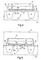
- FIGS. 1 and 2illustrate, respectively, a top view and a cross-section of a MOS transistor obtained using the process described.
- a body 1of semiconductor material, has an insulation region 2 surrounding an active area 3 (FIG. 1).
- a stack 4extends on top of the body 1 and comprises (FIG. 2): a gate oxide region 5 ; a poly1 region 6 ; an interpoly dielectric region 7 ; a poly2 region 8 ; and a silicide region 9 .
- Spacing regions 10are formed at the sides of the stack 4 , and a passivation layer 11 extends on top of the body 1 .
- a plug 12extends through the passivation layer 11 as far as the stack 4 .
- FIG. 1moreover illustrates the shape of the mask for forming the first hole, which has an opening 15 that allows the removal of a portion of the silicide region 9 , the poly2 region 8 , and the interpoly region 7 .
- these regionshave a width smaller than the poly1 region 6 , as may be seen in the cross-section of FIG. 2.
- FIG. 1illustrates the shape of the mask for forming the first hole, which has an opening 15 that allows the removal of a portion of the silicide region 9 , the poly2 region 8 , and the interpoly region 7 .
- these regionshave a width smaller than the poly1 region 6 , as may be seen in the cross-section of FIG. 2.
- FIG. 1moreover illustrates the shape of the mask for forming the first hole, which has an opening 15 that allows the removal of a portion of the silicide region 9 , the poly2 region 8 , and the interpoly region 7 .
- these regionshave a width smaller than the poly1 region 6 , as may be seen
- FIG. 1moreover illustrates the contact mask which has, inter alia, an opening 12 a for the plug 12 , which is staggered with respect to the opening 15 , and in particular is arranged on top of both the remaining portions of the silicide region 9 and the poly2 region 8 and on top of the portion of the poly1 region 6 not overlaid by the silicide region 9 and the poly2 region 8 to ensure that the plug 12 to be electrically connected by the plug 12 .
- the plug 12thus has a step at the silicide layer 9 and, in its bottom part, alongside the regions 7 to 9 , has a cross-sectional area much smaller than that of the top part (on top of the stack 4 ).
- One aim of the present inventionis to provide a manufacturing process which does not require specially designed masks for contacting the two polysilicon layers in the circuitry transistors built using dual polysilicon layer technology.
- MOS deviceand a process for manufacturing MOS devices, as defined in claims 1 and 9 , respectively.
- FIG. 1illustrates the layout of an MOS transistor made with a dedicated mask for connecting the two polysilicon layers
- FIG. 2is a cross-sectional view of the transistor of FIG. 1;
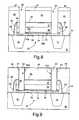
- FIG. 3illustrates the layout of a first embodiment of the transistor according to the invention.
- FIGS. 4 to 9illustrate cross-sectional views, taken along line IX-IX of FIG. 3, in successive manufacturing steps of the transistor of FIG. 3.
- a manufacturing process of self-aligned typecomprising initially standard manufacturing steps, which include: defining the active areas, to form field insulation regions, for example using the shallow-trench technique; depositing a gate oxide layer; depositing a first polycrystalline silicon layer (poly1 layer); depositing an interpoly dielectric layer; depositing a second polycrystalline silicon layer (poly2 layer); depositing a silicide layer; and defining the gate stack, with selective removal of portions of the silicide layer, poly2 layer, interpoly dielectric layer, poly1 layer, and gate oxide layer.
- an LDDlow-doped drain
- spacersare formed on the sides of the gate stack.
- the source and drain regionsare implanted.
- FIG. 4The structure thus obtained is illustrated in FIG. 4 and comprises: a semiconductor body 30 ; a field insulation region 31 delimiting, inside the semiconductor body 30 , an active area 32 ; and a stack 40 , extending on top and at the sides of the active area 32 and on top of the field insulation region 31 .
- the stack 40comprises: a gate oxide region 33 ; a poly1 region 34 , arranged on top of the gate oxide region 33 ; an interpoly dielectric region 35 , arranged on top of the poly1 region 34 and formed by a triple ONO (oxide-nitride-oxide) layer, the triple ONO layer including a first oxide layer 35 a , a nitride layer 35 b , and a second oxide layer 35 c ; a poly2 region 36 , arranged on top of the interpoly dielectric region 35 ; and a silicide region 37 , for example of tungsten silicide, arranged on top of the poly2 region 36 . Spacing regions 38 , for example of oxide and/or nitride, extend at the sides of the stack 40 .
- the stack 40has an elongated shape extending transverse to the active area 32 ; in particular, the stack 40 has a central portion extending on top of the active area 32 and end portions extending on top of the field insulation region 31 .
- the source and drain regions 41are formed, which are illustrated schematically in FIG. 3.
- an etch-stop layer 44is deposited, for instance of nitride, completely coating the stack 40 (and hence the silicide region 37 and the spacing regions 38 ).
- the contact maskis formed, and the contacts are opened.
- a photoresist layeris deposited and defined, so as to have openings where the contacts are to be formed, as illustrated in FIGS. 3 and 6, showing the resist mask 47 and the contact openings 48 .
- the openings for connecting the poly1 region 34 to the poly2 region 36are designated by 48 a .
- the openings 48 aare formed on top of the field insulation region 31 , outside the active area 32 .
- the passivation layer 45is initially etched employing a dedicated chemical process that is highly selective in respect to nitride. Said etch stops on the etch-stop layer 44 on top of the stack 40 . Elsewhere, and hence also at the contacts on the active area, a passivation thickness equal to the height of the gate stack remains. The structure of FIG. 7 is thus obtained.
- a second etchis carried out, using once again the resist mask 47 but with different chemical processes so as to remove, in sequence, the etch-stop nitride layer 44 on top of the stack 40 , portions of the silicide layer 37 , of the poly2 layer 36 and of the interpoly dielectric layer 35 , stopping on the poly1 layer 34 .
- paths 50are formed that extend from the surface of the passivation layer 45 as far as the poly1 layer 34 .
- the residual portion of the passivation layer 45 on top of the contact opening region in the active area (source and drain)is removed by the etch used for the second oxide layer 35 c of the interpoly dielectric 35 .
- the etch-stop nitride layer 44is removed at the contacts, simultaneously with the nitride layer 35 b of the interpoly dielectric 35 , thus uncovering silicon for source and drain contacts.
- a barrier layer 51for example of Ti/TiN
- a metal layer 52for example of tungsten
- the metal layer 52fills the paths 50 to form, together with the barrier layer 51 , first plugs 53 for contacting the various regions of the transistor, and second plugs 53 a in the paths 50 .
- the metal layer 52is then removed from the surface of the passivation layer 45 .
- metal layeris deposited to obtain metal connection regions (metal 1); if envisaged, connections are formed at more than one metallization level, and the customary final operations of fabrication are carried out.
- the plugs 53 aconnect the poly1 region 34 and poly2 region 36 by contacting the poly2 region 36 on the sides of the paths 50 and the poly1 region 34 on the bottom of the paths 50 .
- the plugs 53 aare column-like shaped with a substantially constant cross section without any evident steps due to the staggering between the two masks.
- the contact thus obtainedcan tolerate possible misalignments between the contact mask 47 and the mask for defining the stack 40 as well as any possible process variations.
- the second etching stepetching of layers 34 - 37 and 44 ) is selective with respect to the oxide and, in the case of misalignment, over-etching of the field insulation region 31 is prevented, provided that the area of the plug 53 a lies on top of the stack 40 .
- a possible partial removal of the poly1 region 34does not, on the other hand, adversely affect the electrical connection between the regions 34 , 36 . It follows that the process is reliable and does not present any particular critical aspects.
- Elimination of one maskmoreover enables saving on a manufacture step which has a far from negligible cost, and hence a reduction in fabrication costs.
- the number of poly connection plugs 53 amay vary, and poly connection plugs 53 a may be provided on both sides of the active area 32 .
- the same solutionmay be used for electrically connecting two polysilicon layers in other types of devices integrated together with dual-polysilicon-layer memory cells.
- the path 50may be made also on the edge of the stack 40 , instead of inside the stack 40 .
Landscapes
- Engineering & Computer Science (AREA)
- Manufacturing & Machinery (AREA)
- Internal Circuitry In Semiconductor Integrated Circuit Devices (AREA)
- Semiconductor Memories (AREA)
- Thin Film Transistor (AREA)
Abstract
Description
- This application claims priority to Italian Patent Application No. T02002A 001119 entitled “MOS DEVICE AND PROCESS FOR MANUFACTURING MOS DEVICES USING DUAL-POLYSILICON LAYER TECHNOLOGY”, filed on Dec. 24, 2002, which is incorporated herein by reference in its entirety.[0001]
- 1. Field of the Invention[0002]
- The present invention relates to an MOS device and to a process for manufacturing MOS devices using dual-polysilicon layer technology.[0003]
- 2. Description of the Related Art[0004]
- As is known, simultaneous fabrication in an integrated device of dual-polysilicon layer memory cells and transistors requires removing the polysilicon layer overlying the dielectric and the intermediate dielectric layer in the circuitry area, where the transistors or the electrical connection are made, or forming an electrical connection between the first and the second polysilicon layers for the individual transistors.[0005]
- In particular, U.S. Pat. No. 4,719,184, filed in the name of the present applicant, describes a process, referred to as the double-poly-short-circuited (DPCC) process, which enables short-circuiting the first and second polysilicon layers. According to the aforesaid process, after deposition of the first polysilicon layer and of an interpoly dielectric layer, part of the interpoly dielectric layer is removed in the circuitry area, using a purposely designed mask referred to as “matrix mask”. This mask enables removal of all of the interpoly dielectric on top of the active area of the transistors, or in preset portions, on top of or outside the active area. In this way, when the second polysilicon layer is deposited, it directly contacts the first polysilicon layer in the areas where the interpoly dielectric has been removed.[0006]
- According to a further possibility, the electrical connection between the first and second polysilicon layers is obtained by using a connection region, the production of which requires two masking and etching steps. In fact, first it is necessary to remove part of the second polysilicon layer and of the interpoly dielectric layer so as to expose part of the first polysilicon layer, and then to open the vias through the passivation layer, for forming the connection region.[0007]
- The above solution is represented in FIGS. 1 and 2, which illustrate, respectively, a top view and a cross-section of a MOS transistor obtained using the process described. In FIGS. 1 and 2, a[0008]
body 1, of semiconductor material, has aninsulation region 2 surrounding an active area3 (FIG. 1). Astack 4 extends on top of thebody 1 and comprises (FIG. 2): agate oxide region 5; apoly1 region 6; an interpolydielectric region 7; apoly2 region 8; and asilicide region 9.Spacing regions 10 are formed at the sides of thestack 4, and apassivation layer 11 extends on top of thebody 1. Aplug 12 extends through thepassivation layer 11 as far as thestack 4. - FIG. 1 moreover illustrates the shape of the mask for forming the first hole, which has an[0009]
opening 15 that allows the removal of a portion of thesilicide region 9, thepoly2 region 8, and theinterpoly region 7. Thus, these regions have a width smaller than thepoly1 region 6, as may be seen in the cross-section of FIG. 2. FIG. 1 moreover illustrates the contact mask which has, inter alia, anopening 12afor theplug 12, which is staggered with respect to the opening15, and in particular is arranged on top of both the remaining portions of thesilicide region 9 and thepoly2 region 8 and on top of the portion of thepoly1 region 6 not overlaid by thesilicide region 9 and thepoly2 region 8 to ensure that theplug 12 to be electrically connected by theplug 12. Theplug 12 thus has a step at thesilicide layer 9 and, in its bottom part, alongside theregions 7 to9, has a cross-sectional area much smaller than that of the top part (on top of the stack4). - Both for the solution just described and for the solution described in U.S. Pat. No. 4,719,184, it is disadvantageous that two masks are necessary for electrically connecting poly1 and poly2, and hence the costs of fabrication are high.[0010]
- One aim of the present invention is to provide a manufacturing process which does not require specially designed masks for contacting the two polysilicon layers in the circuitry transistors built using dual polysilicon layer technology.[0011]
- According to the present invention, there are provided a MOS device and a process for manufacturing MOS devices, as defined in[0012]
claims - For a better understanding of the invention, an embodiment thereof is now described, purely by way of non-limiting example, with reference to the attached drawings, wherein:[0013]
- FIG. 1 illustrates the layout of an MOS transistor made with a dedicated mask for connecting the two polysilicon layers;[0014]
- FIG. 2 is a cross-sectional view of the transistor of FIG. 1;[0015]
- FIG. 3 illustrates the layout of a first embodiment of the transistor according to the invention; and[0016]
- FIGS.[0017]4 to9 illustrate cross-sectional views, taken along line IX-IX of FIG. 3, in successive manufacturing steps of the transistor of FIG. 3.
- According to an embodiment of the invention, for electrical connection of the polysilicon layers, just one mask is used, and precisely the mask already used for opening the contacts, as described with reference to FIGS.[0018]3 to9.
- In detail, a manufacturing process of self-aligned type is described herein, comprising initially standard manufacturing steps, which include: defining the active areas, to form field insulation regions, for example using the shallow-trench technique; depositing a gate oxide layer; depositing a first polycrystalline silicon layer (poly1 layer); depositing an interpoly dielectric layer; depositing a second polycrystalline silicon layer (poly2 layer); depositing a silicide layer; and defining the gate stack, with selective removal of portions of the silicide layer, poly2 layer, interpoly dielectric layer, poly1 layer, and gate oxide layer. In the process described, an LDD (low-doped drain) implant is performed, and spacers are formed on the sides of the gate stack. Next, the source and drain regions are implanted.[0019]
- The structure thus obtained is illustrated in FIG. 4 and comprises: a[0020]
semiconductor body 30; afield insulation region 31 delimiting, inside thesemiconductor body 30, anactive area 32; and astack 40, extending on top and at the sides of theactive area 32 and on top of thefield insulation region 31. - The[0021]
stack 40 comprises: agate oxide region 33; apoly1 region 34, arranged on top of thegate oxide region 33; an interpolydielectric region 35, arranged on top of thepoly1 region 34 and formed by a triple ONO (oxide-nitride-oxide) layer, the triple ONO layer including afirst oxide layer 35a, anitride layer 35b, and asecond oxide layer 35c; apoly2 region 36, arranged on top of the interpolydielectric region 35; and asilicide region 37, for example of tungsten silicide, arranged on top of thepoly2 region 36.Spacing regions 38, for example of oxide and/or nitride, extend at the sides of thestack 40. - As is evident from FIG. 3, the[0022]
stack 40 has an elongated shape extending transverse to theactive area 32; in particular, thestack 40 has a central portion extending on top of theactive area 32 and end portions extending on top of thefield insulation region 31. - On the sides of the[0023]
stack 40, inside theactive area 32, the source anddrain regions 41 are formed, which are illustrated schematically in FIG. 3. - Next (see FIG. 5), an etch-[0024]
stop layer 44 is deposited, for instance of nitride, completely coating the stack40 (and hence thesilicide region 37 and the spacing regions38). Subsequently, apassivation layer 45 of dielectric material, for example oxide, is deposited. - Next, the contact mask is formed, and the contacts are opened. To this end, a photoresist layer is deposited and defined, so as to have openings where the contacts are to be formed, as illustrated in FIGS. 3 and 6, showing the[0025]
resist mask 47 and thecontact openings 48. In particular, the openings for connecting thepoly1 region 34 to thepoly2 region 36 are designated by48a. As may be noted, theopenings 48aare formed on top of thefield insulation region 31, outside theactive area 32. - Using the[0026]
resist mask 47, thepassivation layer 45 is initially etched employing a dedicated chemical process that is highly selective in respect to nitride. Said etch stops on the etch-stop layer 44 on top of thestack 40. Elsewhere, and hence also at the contacts on the active area, a passivation thickness equal to the height of the gate stack remains. The structure of FIG. 7 is thus obtained. - Then (see FIG. 8), a second etch is carried out, using once again the[0027]
resist mask 47 but with different chemical processes so as to remove, in sequence, the etch-stop nitride layer 44 on top of thestack 40, portions of thesilicide layer 37, of thepoly2 layer 36 and of the interpolydielectric layer 35, stopping on thepoly1 layer 34. Thereby, at thestack 40,paths 50 are formed that extend from the surface of thepassivation layer 45 as far as thepoly1 layer 34. The residual portion of thepassivation layer 45 on top of the contact opening region in the active area (source and drain), is removed by the etch used for thesecond oxide layer 35cof the interpoly dielectric35. Subsequently, the etch-stop nitride layer 44 is removed at the contacts, simultaneously with thenitride layer 35bof the interpoly dielectric35, thus uncovering silicon for source and drain contacts. - Next (FIG. 9), a[0028]
barrier layer 51, for example of Ti/TiN, and ametal layer 52, for example of tungsten, are deposited in succession. Themetal layer 52 fills thepaths 50 to form, together with thebarrier layer 51, firstplugs 53 for contacting the various regions of the transistor, andsecond plugs 53ain thepaths 50. Themetal layer 52 is then removed from the surface of thepassivation layer 45. - Finally, in a known way, a metal layer is deposited to obtain metal connection regions (metal 1); if envisaged, connections are formed at more than one metallization level, and the customary final operations of fabrication are carried out.[0029]
- In this way, as may be seen from FIG. 9, the[0030]
plugs 53aconnect thepoly1 region 34 andpoly2 region 36 by contacting thepoly2 region 36 on the sides of thepaths 50 and thepoly1 region 34 on the bottom of thepaths 50. - Unlike the[0031]
plugs 12 of FIG. 2, theplugs 53aare column-like shaped with a substantially constant cross section without any evident steps due to the staggering between the two masks. - The device and the process described herein have the advantages outlined hereinafter.[0032]
- Connecting the poly1 and poly2 regions through a plug formed in a single opening of the[0033]
passivation layer 45 and in thestack 40 enables the size of thepath 50 to be reduced down to a lithographic minimum, and in particular plugs to be formed of the same size as the plugs used for the active area and for the gate region of the memory cells. - The contact thus obtained can tolerate possible misalignments between the[0034]
contact mask 47 and the mask for defining thestack 40 as well as any possible process variations. In fact, the second etching step (etching of layers34-37 and44) is selective with respect to the oxide and, in the case of misalignment, over-etching of thefield insulation region 31 is prevented, provided that the area of theplug 53alies on top of thestack 40. - A possible partial removal of the[0035]
poly1 region 34 does not, on the other hand, adversely affect the electrical connection between theregions - Elimination of one mask moreover enables saving on a manufacture step which has a far from negligible cost, and hence a reduction in fabrication costs.[0036]
- Finally, it is evident that modifications and variations may be made to the transistor and to the process described herein, without thereby departing from the scope of the present invention.[0037]
- For example, the number of poly connection plugs[0038]53amay vary, and poly connection plugs53amay be provided on both sides of the
active area 32. Furthermore, the same solution may be used for electrically connecting two polysilicon layers in other types of devices integrated together with dual-polysilicon-layer memory cells. In addition, thepath 50 may be made also on the edge of thestack 40, instead of inside thestack 40. - All of the above U.S. patents, U.S. patent application publications, U.S. patent applications, foreign patents, foreign patent applications and non-patent publications referred to in this specification and/or listed in the Application Data Sheet, are incorporated herein by reference, in their entirety.[0039]
- From the foregoing it will be appreciated that, although specific embodiments of the invention have been described herein for purposes of illustration, various modifications may be made without deviating from the spirit and scope of the invention. Accordingly, the invention is not limited except as by the appended claims.[0040]
Claims (16)
Applications Claiming Priority (2)
| Application Number | Priority Date | Filing Date | Title |
|---|---|---|---|
| ITTO2002A001119 | 2002-12-24 | ||
| IT001119AITTO20021119A1 (en) | 2002-12-24 | 2002-12-24 | MOS DEVICE AND MANUFACTURING PROCEDURE OF |
Publications (2)
| Publication Number | Publication Date |
|---|---|
| US20040188759A1true US20040188759A1 (en) | 2004-09-30 |
| US7023047B2 US7023047B2 (en) | 2006-04-04 |
Family
ID=32448952
Family Applications (1)
| Application Number | Title | Priority Date | Filing Date |
|---|---|---|---|
| US10/745,295Expired - LifetimeUS7023047B2 (en) | 2002-12-24 | 2003-12-23 | MOS device and process for manufacturing MOS devices using dual-polysilicon layer technology |
Country Status (4)
| Country | Link |
|---|---|
| US (1) | US7023047B2 (en) |
| EP (1) | EP1434257B1 (en) |
| DE (1) | DE60334188D1 (en) |
| IT (1) | ITTO20021119A1 (en) |
Cited By (2)
| Publication number | Priority date | Publication date | Assignee | Title |
|---|---|---|---|---|
| US7091570B2 (en) | 2002-12-24 | 2006-08-15 | Stmicroelectronics S.R.L. | MOS device and a process for manufacturing MOS devices using a dual-polysilicon layer technology with side contact |
| US20110298032A1 (en)* | 2009-12-04 | 2011-12-08 | Semiconductor Manufacturing International (Shanghai) Corporation | Array architecture for embedded flash memory devices |
Families Citing this family (1)
| Publication number | Priority date | Publication date | Assignee | Title |
|---|---|---|---|---|
| US7306552B2 (en)* | 2004-12-03 | 2007-12-11 | Samsung Electronics Co., Ltd. | Semiconductor device having load resistor and method of fabricating the same |
Citations (7)
| Publication number | Priority date | Publication date | Assignee | Title |
|---|---|---|---|---|
| US4719184A (en)* | 1984-11-26 | 1988-01-12 | Sgs Microelettronica S.P.A. | Process for the fabrication of integrated structures including nonvolatile memory cells with layers of self-aligned silicon and associated transistors |
| US5326999A (en)* | 1991-11-19 | 1994-07-05 | Samsung Electronics, Co., Ltd. | Non-volatile semiconductor memory device and manufacturing method thereof |
| US5851880A (en)* | 1996-06-14 | 1998-12-22 | Oki Electric Industry Co., Ltd. | Method of making nonvolatile memory elements with selector transistors |
| US6387745B1 (en)* | 1998-02-06 | 2002-05-14 | Mitsubishi Denki Kabushiki Kaisha | Method of making a semiconductor device having a polydiode element |
| US20020127802A1 (en)* | 1999-04-26 | 2002-09-12 | Akira Goda | Nonvolatile semiconductor memory device and method for manufacturing the same |
| US6548857B2 (en)* | 1998-10-21 | 2003-04-15 | Stmicroelectronics S.R.L. | Low resistance contact structure for a select transistor of EEPROM memory cells in a NO-DPCC process |
| US6680514B1 (en)* | 2000-12-20 | 2004-01-20 | International Business Machines Corporation | Contact capping local interconnect |
- 2002
- 2002-12-24ITIT001119Apatent/ITTO20021119A1/enunknown
- 2003
- 2003-12-23USUS10/745,295patent/US7023047B2/ennot_activeExpired - Lifetime
- 2003-12-23EPEP03104939Apatent/EP1434257B1/ennot_activeExpired - Lifetime
- 2003-12-23DEDE60334188Tpatent/DE60334188D1/ennot_activeExpired - Lifetime
Patent Citations (7)
| Publication number | Priority date | Publication date | Assignee | Title |
|---|---|---|---|---|
| US4719184A (en)* | 1984-11-26 | 1988-01-12 | Sgs Microelettronica S.P.A. | Process for the fabrication of integrated structures including nonvolatile memory cells with layers of self-aligned silicon and associated transistors |
| US5326999A (en)* | 1991-11-19 | 1994-07-05 | Samsung Electronics, Co., Ltd. | Non-volatile semiconductor memory device and manufacturing method thereof |
| US5851880A (en)* | 1996-06-14 | 1998-12-22 | Oki Electric Industry Co., Ltd. | Method of making nonvolatile memory elements with selector transistors |
| US6387745B1 (en)* | 1998-02-06 | 2002-05-14 | Mitsubishi Denki Kabushiki Kaisha | Method of making a semiconductor device having a polydiode element |
| US6548857B2 (en)* | 1998-10-21 | 2003-04-15 | Stmicroelectronics S.R.L. | Low resistance contact structure for a select transistor of EEPROM memory cells in a NO-DPCC process |
| US20020127802A1 (en)* | 1999-04-26 | 2002-09-12 | Akira Goda | Nonvolatile semiconductor memory device and method for manufacturing the same |
| US6680514B1 (en)* | 2000-12-20 | 2004-01-20 | International Business Machines Corporation | Contact capping local interconnect |
Cited By (4)
| Publication number | Priority date | Publication date | Assignee | Title |
|---|---|---|---|---|
| US7091570B2 (en) | 2002-12-24 | 2006-08-15 | Stmicroelectronics S.R.L. | MOS device and a process for manufacturing MOS devices using a dual-polysilicon layer technology with side contact |
| US20060246646A1 (en)* | 2002-12-24 | 2006-11-02 | Stmicroelectronics S.R.L. | MOS device and a process for manufacturing MOS devices using a dual-polysilicon layer technology with side contact |
| US20110298032A1 (en)* | 2009-12-04 | 2011-12-08 | Semiconductor Manufacturing International (Shanghai) Corporation | Array architecture for embedded flash memory devices |
| US8536637B2 (en)* | 2009-12-04 | 2013-09-17 | Semiconductor Manufacturing International (Shanghai) Corporation | Array architecture for embedded flash memory devices |
Also Published As
| Publication number | Publication date |
|---|---|
| US7023047B2 (en) | 2006-04-04 |
| EP1434257B1 (en) | 2010-09-15 |
| EP1434257A2 (en) | 2004-06-30 |
| DE60334188D1 (en) | 2010-10-28 |
| ITTO20021119A1 (en) | 2004-06-25 |
| EP1434257A3 (en) | 2004-12-15 |
Similar Documents
| Publication | Publication Date | Title |
|---|---|---|
| US8951860B2 (en) | Manufacturing method of semiconductor device | |
| US6627491B2 (en) | Method of manufacturing non volatile memory device having two charge storage regions | |
| US20030132471A1 (en) | Semiconductor device and method of manufacturing the same | |
| US7829414B2 (en) | Method for manufacturing non-volatile semiconductor memory device, and non-volatile semiconductor memory device | |
| KR19980018838A (en) | A semiconductor device having a tapered isolation insulating film and a method of manufacturing the same. | |
| US6790721B2 (en) | Metal local interconnect self-aligned source flash cell | |
| US7928494B2 (en) | Semiconductor device | |
| US6744139B2 (en) | Semiconductor device | |
| JPH10223770A (en) | Semiconductor device and manufacturing method thereof | |
| US6281076B1 (en) | Method for manufacturing nonvolatile memory device capable of preventing damage to side walls of stacked gate and active region | |
| US7015087B2 (en) | Gate-contact structure and method for forming the same | |
| US20060246646A1 (en) | MOS device and a process for manufacturing MOS devices using a dual-polysilicon layer technology with side contact | |
| US7023047B2 (en) | MOS device and process for manufacturing MOS devices using dual-polysilicon layer technology | |
| US8836008B2 (en) | Semiconductor device and method of manufacturing same | |
| US20040014323A1 (en) | Method of fabricating semiconductor device | |
| US7642595B2 (en) | Nonvolatile semiconductor memory and method of fabrication thereof | |
| US7195968B2 (en) | Method of fabricating semiconductor device | |
| US6458659B1 (en) | Method of fabricating non-volatile memory devices integrated in a semiconductor substrate and organized into memory matrices | |
| US20080197402A1 (en) | Methods of Forming Nonvolatile Memory Devices and Memory Devices Formed Thereby | |
| US7300745B2 (en) | Use of pedestals to fabricate contact openings | |
| JPH088349A (en) | Fabrication of semiconductor device | |
| KR100825770B1 (en) | Self-aligned Common Source Line Fabrication Method in NAND Flash Memory Devices |
Legal Events
| Date | Code | Title | Description |
|---|---|---|---|
| AS | Assignment | Owner name:STMICROELECTRONICS S.R.L., ITALY Free format text:ASSIGNMENT OF ASSIGNORS INTEREST;ASSIGNORS:CONTIN, VALENTINA TESSA;CAIMI, CARLO;MERLANI, DAVIDE;AND OTHERS;REEL/FRAME:014708/0895 Effective date:20040504 | |
| FEPP | Fee payment procedure | Free format text:PAYOR NUMBER ASSIGNED (ORIGINAL EVENT CODE: ASPN); ENTITY STATUS OF PATENT OWNER: LARGE ENTITY | |
| STCF | Information on status: patent grant | Free format text:PATENTED CASE | |
| CC | Certificate of correction | ||
| FPAY | Fee payment | Year of fee payment:4 | |
| AS | Assignment | Owner name:MICRON TECHNOLOGY, INC., IDAHO Free format text:ASSIGNMENT OF ASSIGNORS INTEREST;ASSIGNOR:STMICROELECTRONICS S.R.L.;REEL/FRAME:029186/0761 Effective date:20080206 | |
| FPAY | Fee payment | Year of fee payment:8 | |
| AS | Assignment | Owner name:U.S. BANK NATIONAL ASSOCIATION, AS COLLATERAL AGENT, CALIFORNIA Free format text:SECURITY INTEREST;ASSIGNOR:MICRON TECHNOLOGY, INC.;REEL/FRAME:038669/0001 Effective date:20160426 Owner name:U.S. BANK NATIONAL ASSOCIATION, AS COLLATERAL AGEN Free format text:SECURITY INTEREST;ASSIGNOR:MICRON TECHNOLOGY, INC.;REEL/FRAME:038669/0001 Effective date:20160426 | |
| AS | Assignment | Owner name:MORGAN STANLEY SENIOR FUNDING, INC., AS COLLATERAL AGENT, MARYLAND Free format text:PATENT SECURITY AGREEMENT;ASSIGNOR:MICRON TECHNOLOGY, INC.;REEL/FRAME:038954/0001 Effective date:20160426 Owner name:MORGAN STANLEY SENIOR FUNDING, INC., AS COLLATERAL Free format text:PATENT SECURITY AGREEMENT;ASSIGNOR:MICRON TECHNOLOGY, INC.;REEL/FRAME:038954/0001 Effective date:20160426 | |
| AS | Assignment | Owner name:U.S. BANK NATIONAL ASSOCIATION, AS COLLATERAL AGENT, CALIFORNIA Free format text:CORRECTIVE ASSIGNMENT TO CORRECT THE REPLACE ERRONEOUSLY FILED PATENT #7358718 WITH THE CORRECT PATENT #7358178 PREVIOUSLY RECORDED ON REEL 038669 FRAME 0001. ASSIGNOR(S) HEREBY CONFIRMS THE SECURITY INTEREST;ASSIGNOR:MICRON TECHNOLOGY, INC.;REEL/FRAME:043079/0001 Effective date:20160426 Owner name:U.S. BANK NATIONAL ASSOCIATION, AS COLLATERAL AGEN Free format text:CORRECTIVE ASSIGNMENT TO CORRECT THE REPLACE ERRONEOUSLY FILED PATENT #7358718 WITH THE CORRECT PATENT #7358178 PREVIOUSLY RECORDED ON REEL 038669 FRAME 0001. ASSIGNOR(S) HEREBY CONFIRMS THE SECURITY INTEREST;ASSIGNOR:MICRON TECHNOLOGY, INC.;REEL/FRAME:043079/0001 Effective date:20160426 | |
| MAFP | Maintenance fee payment | Free format text:PAYMENT OF MAINTENANCE FEE, 12TH YEAR, LARGE ENTITY (ORIGINAL EVENT CODE: M1553) Year of fee payment:12 | |
| AS | Assignment | Owner name:JPMORGAN CHASE BANK, N.A., AS COLLATERAL AGENT, ILLINOIS Free format text:SECURITY INTEREST;ASSIGNORS:MICRON TECHNOLOGY, INC.;MICRON SEMICONDUCTOR PRODUCTS, INC.;REEL/FRAME:047540/0001 Effective date:20180703 Owner name:JPMORGAN CHASE BANK, N.A., AS COLLATERAL AGENT, IL Free format text:SECURITY INTEREST;ASSIGNORS:MICRON TECHNOLOGY, INC.;MICRON SEMICONDUCTOR PRODUCTS, INC.;REEL/FRAME:047540/0001 Effective date:20180703 | |
| AS | Assignment | Owner name:MICRON TECHNOLOGY, INC., IDAHO Free format text:RELEASE BY SECURED PARTY;ASSIGNOR:U.S. BANK NATIONAL ASSOCIATION, AS COLLATERAL AGENT;REEL/FRAME:047243/0001 Effective date:20180629 | |
| AS | Assignment | Owner name:MICRON TECHNOLOGY, INC., IDAHO Free format text:RELEASE BY SECURED PARTY;ASSIGNOR:MORGAN STANLEY SENIOR FUNDING, INC., AS COLLATERAL AGENT;REEL/FRAME:050937/0001 Effective date:20190731 | |
| AS | Assignment | Owner name:MICRON TECHNOLOGY, INC., IDAHO Free format text:RELEASE BY SECURED PARTY;ASSIGNOR:JPMORGAN CHASE BANK, N.A., AS COLLATERAL AGENT;REEL/FRAME:051028/0001 Effective date:20190731 Owner name:MICRON SEMICONDUCTOR PRODUCTS, INC., IDAHO Free format text:RELEASE BY SECURED PARTY;ASSIGNOR:JPMORGAN CHASE BANK, N.A., AS COLLATERAL AGENT;REEL/FRAME:051028/0001 Effective date:20190731 |