US20040187917A1 - Transparent electrode, optoelectronic apparatus and devices - Google Patents
Transparent electrode, optoelectronic apparatus and devicesDownload PDFInfo
- Publication number
- US20040187917A1 US20040187917A1US10/403,997US40399703AUS2004187917A1US 20040187917 A1US20040187917 A1US 20040187917A1US 40399703 AUS40399703 AUS 40399703AUS 2004187917 A1US2004187917 A1US 2004187917A1
- Authority
- US
- United States
- Prior art keywords
- layer
- wires
- transparent
- array
- electrode
- Prior art date
- Legal status (The legal status is an assumption and is not a legal conclusion. Google has not performed a legal analysis and makes no representation as to the accuracy of the status listed.)
- Granted
Links
- 230000005693optoelectronicsEffects0.000titleclaimsabstractdescription44
- 239000000463materialSubstances0.000claimsabstractdescription149
- 229920001940conductive polymerPolymers0.000claimsabstractdescription100
- 238000000034methodMethods0.000claimsabstractdescription91
- 239000002322conducting polymerSubstances0.000claimsabstractdescription33
- 229910052751metalInorganic materials0.000claimsdescription52
- 239000002184metalSubstances0.000claimsdescription52
- 230000008569processEffects0.000claimsdescription51
- 239000000758substrateSubstances0.000claimsdescription37
- 239000011148porous materialSubstances0.000claimsdescription34
- 238000011049fillingMethods0.000claimsdescription33
- 239000004065semiconductorSubstances0.000claimsdescription30
- 239000002861polymer materialSubstances0.000claimsdescription18
- 239000011368organic materialSubstances0.000claimsdescription15
- 229910045601alloyInorganic materials0.000claimsdescription14
- 239000000956alloySubstances0.000claimsdescription14
- 230000015572biosynthetic processEffects0.000claimsdescription14
- 230000000295complement effectEffects0.000claimsdescription14
- 238000012546transferMethods0.000claimsdescription14
- 229920001609Poly(3,4-ethylenedioxythiophene)Polymers0.000claimsdescription13
- 239000000853adhesiveSubstances0.000claimsdescription11
- 230000001070adhesive effectEffects0.000claimsdescription11
- 238000003786synthesis reactionMethods0.000claimsdescription11
- 229920000767polyanilinePolymers0.000claimsdescription10
- 239000004020conductorSubstances0.000claimsdescription9
- 229910010272inorganic materialInorganic materials0.000claimsdescription9
- 239000002105nanoparticleSubstances0.000claimsdescription9
- 229920000128polypyrrolePolymers0.000claimsdescription9
- 239000011147inorganic materialSubstances0.000claimsdescription8
- 229910052500inorganic mineralInorganic materials0.000claimsdescription8
- 239000011707mineralSubstances0.000claimsdescription8
- 150000004703alkoxidesChemical class0.000claimsdescription7
- 239000000499gelSubstances0.000claimsdescription7
- 229920000123polythiophenePolymers0.000claimsdescription7
- 239000003795chemical substances by applicationSubstances0.000claimsdescription5
- 150000004820halidesChemical class0.000claimsdescription4
- 229920002521macromoleculePolymers0.000claimsdescription4
- 239000002086nanomaterialSubstances0.000claimsdescription4
- 230000000712assemblyEffects0.000claimsdescription3
- 238000000429assemblyMethods0.000claimsdescription3
- 238000005470impregnationMethods0.000claimsdescription3
- 230000002687intercalationEffects0.000claimsdescription3
- 238000009830intercalationMethods0.000claimsdescription3
- 229920000642polymerPolymers0.000abstractdescription38
- 239000010410layerSubstances0.000description298
- 210000004027cellAnatomy0.000description51
- 239000000243solutionSubstances0.000description35
- GWEVSGVZZGPLCZ-UHFFFAOYSA-NTitan oxideChemical compoundO=[Ti]=OGWEVSGVZZGPLCZ-UHFFFAOYSA-N0.000description31
- 239000010408filmSubstances0.000description31
- -1for exampleSubstances0.000description24
- 230000005855radiationEffects0.000description24
- 239000008393encapsulating agentSubstances0.000description20
- 238000004519manufacturing processMethods0.000description19
- 238000012545processingMethods0.000description17
- 238000000576coating methodMethods0.000description16
- 238000010586diagramMethods0.000description16
- 239000011248coating agentSubstances0.000description15
- 239000007772electrode materialSubstances0.000description13
- 239000011888foilSubstances0.000description13
- 239000000203mixtureSubstances0.000description13
- 239000004094surface-active agentSubstances0.000description13
- 238000013459approachMethods0.000description12
- 239000000975dyeSubstances0.000description12
- 239000010949copperSubstances0.000description11
- 238000000151depositionMethods0.000description10
- 229910052802copperInorganic materials0.000description9
- 238000007639printingMethods0.000description9
- 238000003491arrayMethods0.000description8
- 150000001875compoundsChemical class0.000description8
- 229920000547conjugated polymerPolymers0.000description8
- 238000007646gravure printingMethods0.000description8
- 238000003475laminationMethods0.000description8
- 239000002243precursorSubstances0.000description8
- 229910052710siliconInorganic materials0.000description8
- 239000010703siliconSubstances0.000description8
- 239000010409thin filmSubstances0.000description8
- XUIMIQQOPSSXEZ-UHFFFAOYSA-NSiliconChemical compound[Si]XUIMIQQOPSSXEZ-UHFFFAOYSA-N0.000description7
- 239000012790adhesive layerSubstances0.000description7
- 238000000137annealingMethods0.000description7
- 238000005538encapsulationMethods0.000description7
- 229910052709silverInorganic materials0.000description7
- OKTJSMMVPCPJKN-UHFFFAOYSA-NCarbonChemical compound[C]OKTJSMMVPCPJKN-UHFFFAOYSA-N0.000description6
- RYGMFSIKBFXOCR-UHFFFAOYSA-NCopperChemical compound[Cu]RYGMFSIKBFXOCR-UHFFFAOYSA-N0.000description6
- HEMHJVSKTPXQMS-UHFFFAOYSA-MSodium hydroxideChemical compound[OH-].[Na+]HEMHJVSKTPXQMS-UHFFFAOYSA-M0.000description6
- 229910052782aluminiumInorganic materials0.000description6
- 229910052799carbonInorganic materials0.000description6
- 230000006835compressionEffects0.000description6
- 238000007906compressionMethods0.000description6
- 229920001577copolymerPolymers0.000description6
- 239000000835fiberSubstances0.000description6
- 239000002904solventSubstances0.000description6
- 238000004544sputter depositionMethods0.000description6
- 230000008021depositionEffects0.000description5
- 239000011521glassSubstances0.000description5
- 238000010438heat treatmentMethods0.000description5
- 150000002739metalsChemical class0.000description5
- 229920003023plasticPolymers0.000description5
- 239000004033plasticSubstances0.000description5
- 239000000725suspensionSubstances0.000description5
- 239000012780transparent materialSubstances0.000description5
- MARUHZGHZWCEQU-UHFFFAOYSA-N5-phenyl-2h-tetrazoleChemical compoundC1=CC=CC=C1C1=NNN=N1MARUHZGHZWCEQU-UHFFFAOYSA-N0.000description4
- VEXZGXHMUGYJMC-UHFFFAOYSA-NHydrochloric acidChemical compoundClVEXZGXHMUGYJMC-UHFFFAOYSA-N0.000description4
- BQCADISMDOOEFD-UHFFFAOYSA-NSilverChemical compound[Ag]BQCADISMDOOEFD-UHFFFAOYSA-N0.000description4
- XLOMVQKBTHCTTD-UHFFFAOYSA-NZinc monoxideChemical compound[Zn]=OXLOMVQKBTHCTTD-UHFFFAOYSA-N0.000description4
- 229920001400block copolymerPolymers0.000description4
- 239000006185dispersionSubstances0.000description4
- PCHJSUWPFVWCPO-UHFFFAOYSA-NgoldChemical compound[Au]PCHJSUWPFVWCPO-UHFFFAOYSA-N0.000description4
- 229910052737goldInorganic materials0.000description4
- 239000010931goldSubstances0.000description4
- 238000007641inkjet printingMethods0.000description4
- 239000011810insulating materialSubstances0.000description4
- 239000012212insulatorSubstances0.000description4
- 230000003993interactionEffects0.000description4
- 239000000178monomerSubstances0.000description4
- 150000002979perylenesChemical class0.000description4
- 229920002959polymer blendPolymers0.000description4
- 229920005989resinPolymers0.000description4
- 239000011347resinSubstances0.000description4
- 238000007650screen-printingMethods0.000description4
- 239000004332silverSubstances0.000description4
- 238000010129solution processingMethods0.000description4
- 238000005507sprayingMethods0.000description4
- 239000000126substanceSubstances0.000description4
- XLYOFNOQVPJJNP-UHFFFAOYSA-NwaterSubstancesOXLYOFNOQVPJJNP-UHFFFAOYSA-N0.000description4
- WUPHOULIZUERAE-UHFFFAOYSA-N3-(oxolan-2-yl)propanoic acidChemical compoundOC(=O)CCC1CCCO1WUPHOULIZUERAE-UHFFFAOYSA-N0.000description3
- 229920002799BoPETPolymers0.000description3
- PXHVJJICTQNCMI-UHFFFAOYSA-NNickelChemical compound[Ni]PXHVJJICTQNCMI-UHFFFAOYSA-N0.000description3
- QAOWNCQODCNURD-UHFFFAOYSA-NSulfuric acidChemical compoundOS(O)(=O)=OQAOWNCQODCNURD-UHFFFAOYSA-N0.000description3
- ZMANZCXQSJIPKH-UHFFFAOYSA-NTriethylamineChemical compoundCCN(CC)CCZMANZCXQSJIPKH-UHFFFAOYSA-N0.000description3
- XAGFODPZIPBFFR-UHFFFAOYSA-NaluminiumChemical compound[Al]XAGFODPZIPBFFR-UHFFFAOYSA-N0.000description3
- 125000004429atomChemical group0.000description3
- QVGXLLKOCUKJST-UHFFFAOYSA-Natomic oxygenChemical compound[O]QVGXLLKOCUKJST-UHFFFAOYSA-N0.000description3
- 230000005540biological transmissionEffects0.000description3
- 229910052980cadmium sulfideInorganic materials0.000description3
- 239000000919ceramicSubstances0.000description3
- 239000002800charge carrierSubstances0.000description3
- 238000006243chemical reactionMethods0.000description3
- 239000013078crystalSubstances0.000description3
- 238000003618dip coatingMethods0.000description3
- 238000001035dryingMethods0.000description3
- 239000000839emulsionSubstances0.000description3
- 238000001704evaporationMethods0.000description3
- 239000003292glueSubstances0.000description3
- 238000004770highest occupied molecular orbitalMethods0.000description3
- 229910052739hydrogenInorganic materials0.000description3
- 239000001257hydrogenSubstances0.000description3
- 238000004768lowest unoccupied molecular orbitalMethods0.000description3
- 150000004767nitridesChemical class0.000description3
- QGLKJKCYBOYXKC-UHFFFAOYSA-NnonaoxidotritungstenChemical compoundO=[W]1(=O)O[W](=O)(=O)O[W](=O)(=O)O1QGLKJKCYBOYXKC-UHFFFAOYSA-N0.000description3
- 229910052760oxygenInorganic materials0.000description3
- 239000001301oxygenSubstances0.000description3
- 239000000049pigmentSubstances0.000description3
- 229920001197polyacetylenePolymers0.000description3
- 238000004528spin coatingMethods0.000description3
- 150000003413spiro compoundsChemical class0.000description3
- BFKJFAAPBSQJPD-UHFFFAOYSA-NtetrafluoroetheneChemical groupFC(F)=C(F)FBFKJFAAPBSQJPD-UHFFFAOYSA-N0.000description3
- 229910052718tinInorganic materials0.000description3
- 239000011135tinSubstances0.000description3
- 229910001930tungsten oxideInorganic materials0.000description3
- IJGRMHOSHXDMSA-UHFFFAOYSA-NAtomic nitrogenChemical compoundN#NIJGRMHOSHXDMSA-UHFFFAOYSA-N0.000description2
- LZZYPRNAOMGNLH-UHFFFAOYSA-MCetrimonium bromideChemical compound[Br-].CCCCCCCCCCCCCCCC[N+](C)(C)CLZZYPRNAOMGNLH-UHFFFAOYSA-M0.000description2
- 229910016553CuOxInorganic materials0.000description2
- RTZKZFJDLAIYFH-UHFFFAOYSA-NDiethyl etherChemical compoundCCOCCRTZKZFJDLAIYFH-UHFFFAOYSA-N0.000description2
- 239000004593EpoxySubstances0.000description2
- LFQSCWFLJHTTHZ-UHFFFAOYSA-NEthanolChemical compoundCCOLFQSCWFLJHTTHZ-UHFFFAOYSA-N0.000description2
- 229910001111Fine metalInorganic materials0.000description2
- YCKRFDGAMUMZLT-UHFFFAOYSA-NFluorine atomChemical compound[F]YCKRFDGAMUMZLT-UHFFFAOYSA-N0.000description2
- UFHFLCQGNIYNRP-UHFFFAOYSA-NHydrogenChemical compound[H][H]UFHFLCQGNIYNRP-UHFFFAOYSA-N0.000description2
- VVQNEPGJFQJSBK-UHFFFAOYSA-NMethyl methacrylateChemical compoundCOC(=O)C(C)=CVVQNEPGJFQJSBK-UHFFFAOYSA-N0.000description2
- 239000005041Mylar™Substances0.000description2
- GRYLNZFGIOXLOG-UHFFFAOYSA-NNitric acidChemical compoundO[N+]([O-])=OGRYLNZFGIOXLOG-UHFFFAOYSA-N0.000description2
- 229910019142PO4Inorganic materials0.000description2
- KDLHZDBZIXYQEI-UHFFFAOYSA-NPalladiumChemical compound[Pd]KDLHZDBZIXYQEI-UHFFFAOYSA-N0.000description2
- ABLZXFCXXLZCGV-UHFFFAOYSA-NPhosphorous acidChemical classOP(O)=OABLZXFCXXLZCGV-UHFFFAOYSA-N0.000description2
- 229920000265PolyparaphenylenePolymers0.000description2
- 239000004793PolystyreneSubstances0.000description2
- VYPSYNLAJGMNEJ-UHFFFAOYSA-NSilicium dioxideChemical compoundO=[Si]=OVYPSYNLAJGMNEJ-UHFFFAOYSA-N0.000description2
- 229910006854SnOxInorganic materials0.000description2
- 229910000831SteelInorganic materials0.000description2
- BOTDANWDWHJENH-UHFFFAOYSA-NTetraethyl orthosilicateChemical compoundCCO[Si](OCC)(OCC)OCCBOTDANWDWHJENH-UHFFFAOYSA-N0.000description2
- ATJFFYVFTNAWJD-UHFFFAOYSA-NTinChemical compound[Sn]ATJFFYVFTNAWJD-UHFFFAOYSA-N0.000description2
- MCMNRKCIXSYSNV-UHFFFAOYSA-NZirconium dioxideChemical compoundO=[Zr]=OMCMNRKCIXSYSNV-UHFFFAOYSA-N0.000description2
- 229910007667ZnOxInorganic materials0.000description2
- YRKCREAYFQTBPV-UHFFFAOYSA-NacetylacetoneChemical compoundCC(=O)CC(C)=OYRKCREAYFQTBPV-UHFFFAOYSA-N0.000description2
- HSFWRNGVRCDJHI-UHFFFAOYSA-Nalpha-acetyleneNatural productsC#CHSFWRNGVRCDJHI-UHFFFAOYSA-N0.000description2
- DQXBYHZEEUGOBF-UHFFFAOYSA-Nbut-3-enoic acid;etheneChemical compoundC=C.OC(=O)CC=CDQXBYHZEEUGOBF-UHFFFAOYSA-N0.000description2
- AQCDIIAORKRFCD-UHFFFAOYSA-Ncadmium selenideChemical compound[Cd]=[Se]AQCDIIAORKRFCD-UHFFFAOYSA-N0.000description2
- 238000005253claddingMethods0.000description2
- 238000009833condensationMethods0.000description2
- 230000005494condensationEffects0.000description2
- 238000010276constructionMethods0.000description2
- 230000007797corrosionEffects0.000description2
- 238000005260corrosionMethods0.000description2
- 238000005137deposition processMethods0.000description2
- GNTDGMZSJNCJKK-UHFFFAOYSA-Ndivanadium pentaoxideChemical compoundO=[V](=O)O[V](=O)=OGNTDGMZSJNCJKK-UHFFFAOYSA-N0.000description2
- 238000007606doctor blade methodMethods0.000description2
- 230000000694effectsEffects0.000description2
- 238000004070electrodepositionMethods0.000description2
- 238000005566electron beam evaporationMethods0.000description2
- 238000004146energy storageMethods0.000description2
- 239000005038ethylene vinyl acetateSubstances0.000description2
- 230000008020evaporationEffects0.000description2
- 238000000605extractionMethods0.000description2
- 238000001125extrusionMethods0.000description2
- 239000004744fabricSubstances0.000description2
- 239000011737fluorineSubstances0.000description2
- 229910052731fluorineInorganic materials0.000description2
- 125000000524functional groupChemical group0.000description2
- 230000007062hydrolysisEffects0.000description2
- 238000006460hydrolysis reactionMethods0.000description2
- 230000006872improvementEffects0.000description2
- AMGQUBHHOARCQH-UHFFFAOYSA-Nindium;oxotinChemical compound[In].[Sn]=OAMGQUBHHOARCQH-UHFFFAOYSA-N0.000description2
- 239000003112inhibitorSubstances0.000description2
- 238000002347injectionMethods0.000description2
- 239000007924injectionSubstances0.000description2
- MRELNEQAGSRDBK-UHFFFAOYSA-Nlanthanum(3+);oxygen(2-)Chemical compound[O-2].[O-2].[O-2].[La+3].[La+3]MRELNEQAGSRDBK-UHFFFAOYSA-N0.000description2
- 239000004973liquid crystal related substanceSubstances0.000description2
- 239000011244liquid electrolyteSubstances0.000description2
- 230000008018meltingEffects0.000description2
- 238000002844meltingMethods0.000description2
- 229910001092metal group alloyInorganic materials0.000description2
- 229910052750molybdenumInorganic materials0.000description2
- 229910052759nickelInorganic materials0.000description2
- 229910052758niobiumInorganic materials0.000description2
- 239000010955niobiumSubstances0.000description2
- 229910017604nitric acidInorganic materials0.000description2
- 230000003287optical effectEffects0.000description2
- 239000012044organic layerSubstances0.000description2
- 239000002245particleSubstances0.000description2
- 235000021317phosphateNutrition0.000description2
- 150000003013phosphoric acid derivativesChemical class0.000description2
- BASFCYQUMIYNBI-UHFFFAOYSA-NplatinumChemical compound[Pt]BASFCYQUMIYNBI-UHFFFAOYSA-N0.000description2
- 229920001200poly(ethylene-vinyl acetate)Polymers0.000description2
- 229920000139polyethylene terephthalatePolymers0.000description2
- 239000005020polyethylene terephthalateSubstances0.000description2
- 229920002098polyfluorenePolymers0.000description2
- 238000006116polymerization reactionMethods0.000description2
- 229920002223polystyrenePolymers0.000description2
- 229920002620polyvinyl fluoridePolymers0.000description2
- 239000002356single layerSubstances0.000description2
- 241000894007speciesSpecies0.000description2
- 239000007921spraySubstances0.000description2
- 239000010959steelSubstances0.000description2
- 229910052712strontiumInorganic materials0.000description2
- IATRAKWUXMZMIY-UHFFFAOYSA-Nstrontium oxideChemical compound[O-2].[Sr+2]IATRAKWUXMZMIY-UHFFFAOYSA-N0.000description2
- 239000012815thermoplastic materialSubstances0.000description2
- 229910052719titaniumInorganic materials0.000description2
- 239000010936titaniumSubstances0.000description2
- 229910052721tungstenInorganic materials0.000description2
- 235000012431wafersNutrition0.000description2
- 229910052725zincInorganic materials0.000description2
- 239000011701zincSubstances0.000description2
- 239000011787zinc oxideSubstances0.000description2
- 229910052726zirconiumInorganic materials0.000description2
- NLMKTBGFQGKQEV-UHFFFAOYSA-N2-[2-[2-[2-[2-[2-[2-[2-[2-[2-[2-[2-[2-[2-[2-[2-[2-[2-[2-(2-hexadecoxyethoxy)ethoxy]ethoxy]ethoxy]ethoxy]ethoxy]ethoxy]ethoxy]ethoxy]ethoxy]ethoxy]ethoxy]ethoxy]ethoxy]ethoxy]ethoxy]ethoxy]ethoxy]ethoxy]ethanolChemical compoundCCCCCCCCCCCCCCCCOCCOCCOCCOCCOCCOCCOCCOCCOCCOCCOCCOCCOCCOCCOCCOCCOCCOCCOCCOCCONLMKTBGFQGKQEV-UHFFFAOYSA-N0.000description1
- OYPRJOBELJOOCE-UHFFFAOYSA-NCalciumChemical compound[Ca]OYPRJOBELJOOCE-UHFFFAOYSA-N0.000description1
- 229910002535CuZnInorganic materials0.000description1
- 102000004190EnzymesHuman genes0.000description1
- 108090000790EnzymesProteins0.000description1
- VGGSQFUCUMXWEO-UHFFFAOYSA-NEtheneChemical compoundC=CVGGSQFUCUMXWEO-UHFFFAOYSA-N0.000description1
- 239000005977EthyleneSubstances0.000description1
- 206010073306Exposure to radiationDiseases0.000description1
- 229910001218Gallium arsenideInorganic materials0.000description1
- 241000264877Hippospongia communisSpecies0.000description1
- ZOKXTWBITQBERF-UHFFFAOYSA-NMolybdenumChemical compound[Mo]ZOKXTWBITQBERF-UHFFFAOYSA-N0.000description1
- 229920006367NeoflonPolymers0.000description1
- 229910000943NiAlInorganic materials0.000description1
- 229910001252Pd alloyInorganic materials0.000description1
- 229920002415Pluronic P-123Polymers0.000description1
- 239000004952PolyamideSubstances0.000description1
- 229920002873PolyethyleniminePolymers0.000description1
- 239000004743PolypropyleneSubstances0.000description1
- NPXOKRUENSOPAO-UHFFFAOYSA-NRaney nickelChemical compound[Al].[Ni]NPXOKRUENSOPAO-UHFFFAOYSA-N0.000description1
- KJTLSVCANCCWHF-UHFFFAOYSA-NRutheniumChemical compound[Ru]KJTLSVCANCCWHF-UHFFFAOYSA-N0.000description1
- 229910052581Si3N4Inorganic materials0.000description1
- 239000004809TeflonSubstances0.000description1
- 229920006362Teflon®Polymers0.000description1
- 229920006355TefzelPolymers0.000description1
- 229920004933Terylene®Polymers0.000description1
- RTAQQCXQSZGOHL-UHFFFAOYSA-NTitaniumChemical compound[Ti]RTAQQCXQSZGOHL-UHFFFAOYSA-N0.000description1
- HCHKCACWOHOZIP-UHFFFAOYSA-NZincChemical compound[Zn]HCHKCACWOHOZIP-UHFFFAOYSA-N0.000description1
- QCWXUUIWCKQGHC-UHFFFAOYSA-NZirconiumChemical compound[Zr]QCWXUUIWCKQGHC-UHFFFAOYSA-N0.000description1
- 239000006096absorbing agentSubstances0.000description1
- 239000002253acidSubstances0.000description1
- 239000003929acidic solutionSubstances0.000description1
- 150000007513acidsChemical class0.000description1
- 230000009471actionEffects0.000description1
- 125000003545alkoxy groupChemical group0.000description1
- 230000004075alterationEffects0.000description1
- PNEYBMLMFCGWSK-UHFFFAOYSA-Naluminium oxideInorganic materials[O-2].[O-2].[O-2].[Al+3].[Al+3]PNEYBMLMFCGWSK-UHFFFAOYSA-N0.000description1
- 150000001412aminesChemical class0.000description1
- 229920000469amphiphilic block copolymerPolymers0.000description1
- 230000003667anti-reflective effectEffects0.000description1
- 125000003118aryl groupChemical group0.000description1
- 239000000987azo dyeSubstances0.000description1
- 229910052788bariumInorganic materials0.000description1
- 230000004888barrier functionEffects0.000description1
- 229910052793cadmiumInorganic materials0.000description1
- 239000011575calciumSubstances0.000description1
- ODINCKMPIJJUCX-UHFFFAOYSA-Ncalcium oxideInorganic materials[Ca]=OODINCKMPIJJUCX-UHFFFAOYSA-N0.000description1
- 239000003990capacitorSubstances0.000description1
- 150000005323carbonate saltsChemical class0.000description1
- 239000002738chelating agentSubstances0.000description1
- 229910052729chemical elementInorganic materials0.000description1
- 238000001311chemical methods and processMethods0.000description1
- 239000011247coating layerSubstances0.000description1
- 229910052681coesiteInorganic materials0.000description1
- 239000000084colloidal systemSubstances0.000description1
- 230000002860competitive effectEffects0.000description1
- 238000006482condensation reactionMethods0.000description1
- 239000000470constituentSubstances0.000description1
- 238000010924continuous productionMethods0.000description1
- PMHQVHHXPFUNSP-UHFFFAOYSA-Mcopper(1+);methylsulfanylmethane;bromideChemical compoundBr[Cu].CSCPMHQVHHXPFUNSP-UHFFFAOYSA-M0.000description1
- 238000005536corrosion preventionMethods0.000description1
- 229910052906cristobaliteInorganic materials0.000description1
- 238000004132cross linkingMethods0.000description1
- 238000005520cutting processMethods0.000description1
- 238000013461designMethods0.000description1
- 238000011161developmentMethods0.000description1
- 230000018109developmental processEffects0.000description1
- 239000003989dielectric materialSubstances0.000description1
- 239000002019doping agentSubstances0.000description1
- 239000012777electrically insulating materialSubstances0.000description1
- 230000005611electricityEffects0.000description1
- 238000005868electrolysis reactionMethods0.000description1
- 239000003822epoxy resinSubstances0.000description1
- QHSJIZLJUFMIFP-UHFFFAOYSA-Nethene;1,1,2,2-tetrafluoroetheneChemical compoundC=C.FC(F)=C(F)FQHSJIZLJUFMIFP-UHFFFAOYSA-N0.000description1
- 229920001038ethylene copolymerPolymers0.000description1
- 229920000840ethylene tetrafluoroethylene copolymerPolymers0.000description1
- 230000002349favourable effectEffects0.000description1
- 239000000945fillerSubstances0.000description1
- 229920001519homopolymerPolymers0.000description1
- 150000002431hydrogenChemical class0.000description1
- 238000001764infiltrationMethods0.000description1
- 230000008595infiltrationEffects0.000description1
- 150000002484inorganic compoundsChemical class0.000description1
- 239000013385inorganic frameworkSubstances0.000description1
- 229920000592inorganic polymerPolymers0.000description1
- 229910000765intermetallicInorganic materials0.000description1
- 238000007733ion platingMethods0.000description1
- 150000002500ionsChemical class0.000description1
- 229910052742ironInorganic materials0.000description1
- 230000001788irregularEffects0.000description1
- 238000010030laminatingMethods0.000description1
- 229910052746lanthanumInorganic materials0.000description1
- FZLIPJUXYLNCLC-UHFFFAOYSA-Nlanthanum atomChemical compound[La]FZLIPJUXYLNCLC-UHFFFAOYSA-N0.000description1
- 239000004816latexSubstances0.000description1
- 229920000126latexPolymers0.000description1
- 229910052745leadInorganic materials0.000description1
- 239000011133leadSubstances0.000description1
- 239000007788liquidSubstances0.000description1
- 238000001459lithographyMethods0.000description1
- 239000012528membraneSubstances0.000description1
- 230000005499meniscusEffects0.000description1
- 150000001247metal acetylidesChemical class0.000description1
- 239000007769metal materialSubstances0.000description1
- 229910044991metal oxideInorganic materials0.000description1
- 150000004706metal oxidesChemical class0.000description1
- 239000002923metal particleSubstances0.000description1
- 238000001465metallisationMethods0.000description1
- 239000004530micro-emulsionSubstances0.000description1
- 230000004048modificationEffects0.000description1
- 238000012986modificationMethods0.000description1
- 238000004776molecular orbitalMethods0.000description1
- AIPBSZJAQGGCPD-UHFFFAOYSA-Nmolport-035-677-503Chemical compoundC=12C3=CC=C(C(N(C(CC)CC)C4=O)=O)C2=C4C=CC=1C1=CC=C2C(=O)N(C(CC)CC)C(=O)C4=CC=C3C1=C42AIPBSZJAQGGCPD-UHFFFAOYSA-N0.000description1
- 239000011733molybdenumSubstances0.000description1
- 239000002159nanocrystalSubstances0.000description1
- 239000002073nanorodSubstances0.000description1
- 239000002071nanotubeSubstances0.000description1
- GUCVJGMIXFAOAE-UHFFFAOYSA-Nniobium atomChemical compound[Nb]GUCVJGMIXFAOAE-UHFFFAOYSA-N0.000description1
- 229910000484niobium oxideInorganic materials0.000description1
- URLJKFSTXLNXLG-UHFFFAOYSA-Nniobium(5+);oxygen(2-)Chemical compound[O-2].[O-2].[O-2].[O-2].[O-2].[Nb+5].[Nb+5]URLJKFSTXLNXLG-UHFFFAOYSA-N0.000description1
- 229910052757nitrogenInorganic materials0.000description1
- 239000013384organic frameworkSubstances0.000description1
- 239000012860organic pigmentSubstances0.000description1
- 239000003960organic solventSubstances0.000description1
- 125000002524organometallic groupChemical group0.000description1
- 230000003647oxidationEffects0.000description1
- 238000007254oxidation reactionMethods0.000description1
- TWNQGVIAIRXVLR-UHFFFAOYSA-Noxo(oxoalumanyloxy)alumaneChemical compoundO=[Al]O[Al]=OTWNQGVIAIRXVLR-UHFFFAOYSA-N0.000description1
- RVTZCBVAJQQJTK-UHFFFAOYSA-Noxygen(2-);zirconium(4+)Chemical compound[O-2].[O-2].[Zr+4]RVTZCBVAJQQJTK-UHFFFAOYSA-N0.000description1
- 229910052763palladiumInorganic materials0.000description1
- SWELZOZIOHGSPA-UHFFFAOYSA-Npalladium silverChemical compound[Pd].[Ag]SWELZOZIOHGSPA-UHFFFAOYSA-N0.000description1
- 150000002978peroxidesChemical class0.000description1
- IEQIEDJGQAUEQZ-UHFFFAOYSA-NphthalocyanineChemical compoundN1C(N=C2C3=CC=CC=C3C(N=C3C4=CC=CC=C4C(=N4)N3)=N2)=C(C=CC=C2)C2=C1N=C1C2=CC=CC=C2C4=N1IEQIEDJGQAUEQZ-UHFFFAOYSA-N0.000description1
- 238000007747platingMethods0.000description1
- 229910052697platinumInorganic materials0.000description1
- 229920001983poloxamerPolymers0.000description1
- 229920001992poloxamer 407Polymers0.000description1
- 229920000548poly(silane) polymerPolymers0.000description1
- 229920002647polyamidePolymers0.000description1
- 229920000515polycarbonatePolymers0.000description1
- 239000004417polycarbonateSubstances0.000description1
- 238000006068polycondensation reactionMethods0.000description1
- 229920000647polyepoxidePolymers0.000description1
- 229920000728polyesterPolymers0.000description1
- 239000005518polymer electrolyteSubstances0.000description1
- 229920001155polypropylenePolymers0.000description1
- 229920001296polysiloxanePolymers0.000description1
- 229920002635polyurethanePolymers0.000description1
- 239000004814polyurethaneSubstances0.000description1
- UKDIAJWKFXFVFG-UHFFFAOYSA-Npotassium;oxido(dioxo)niobiumChemical compound[K+].[O-][Nb](=O)=OUKDIAJWKFXFVFG-UHFFFAOYSA-N0.000description1
- 238000010248power generationMethods0.000description1
- 239000010970precious metalSubstances0.000description1
- 230000002265preventionEffects0.000description1
- 238000005546reactive sputteringMethods0.000description1
- 238000012552reviewMethods0.000description1
- 229910052707rutheniumInorganic materials0.000description1
- 230000001235sensitizing effectEffects0.000description1
- 239000005266side chain polymerSubstances0.000description1
- 229910002028silica xerogelInorganic materials0.000description1
- HBMJWWWQQXIZIP-UHFFFAOYSA-Nsilicon carbideChemical compound[Si+]#[C-]HBMJWWWQQXIZIP-UHFFFAOYSA-N0.000description1
- 229910010271silicon carbideInorganic materials0.000description1
- 239000000377silicon dioxideSubstances0.000description1
- HQVNEWCFYHHQES-UHFFFAOYSA-Nsilicon nitrideChemical compoundN12[Si]34N5[Si]62N3[Si]51N64HQVNEWCFYHHQES-UHFFFAOYSA-N0.000description1
- GROMGGTZECPEKN-UHFFFAOYSA-Nsodium metatitanateChemical compound[Na+].[Na+].[O-][Ti](=O)O[Ti](=O)O[Ti]([O-])=OGROMGGTZECPEKN-UHFFFAOYSA-N0.000description1
- 229910000679solderInorganic materials0.000description1
- 239000007787solidSubstances0.000description1
- 239000007784solid electrolyteSubstances0.000description1
- 125000006850spacer groupChemical group0.000description1
- 125000003003spiro groupChemical group0.000description1
- 229910001220stainless steelInorganic materials0.000description1
- 239000010935stainless steelSubstances0.000description1
- 229910052682stishoviteInorganic materials0.000description1
- 238000003860storageMethods0.000description1
- CIOAGBVUUVVLOB-UHFFFAOYSA-Nstrontium atomChemical compound[Sr]CIOAGBVUUVVLOB-UHFFFAOYSA-N0.000description1
- 150000004763sulfidesChemical class0.000description1
- BDHFUVZGWQCTTF-UHFFFAOYSA-Nsulfonic acidChemical compoundOS(=O)=OBDHFUVZGWQCTTF-UHFFFAOYSA-N0.000description1
- 230000003746surface roughnessEffects0.000description1
- 229920001897terpolymerPolymers0.000description1
- XOLBLPGZBRYERU-UHFFFAOYSA-Ntin dioxideChemical compoundO=[Sn]=OXOLBLPGZBRYERU-UHFFFAOYSA-N0.000description1
- 229910001887tin oxideInorganic materials0.000description1
- OGIDPMRJRNCKJF-UHFFFAOYSA-Ntitanium oxideInorganic materials[Ti]=OOGIDPMRJRNCKJF-UHFFFAOYSA-N0.000description1
- 229910052723transition metalInorganic materials0.000description1
- 150000003624transition metalsChemical class0.000description1
- 229910052905tridymiteInorganic materials0.000description1
- WFKWXMTUELFFGS-UHFFFAOYSA-NtungstenChemical compound[W]WFKWXMTUELFFGS-UHFFFAOYSA-N0.000description1
- 239000010937tungstenSubstances0.000description1
- 238000001771vacuum depositionMethods0.000description1
- 229910052720vanadiumInorganic materials0.000description1
- 229910052727yttriumInorganic materials0.000description1
- 239000010457zeoliteSubstances0.000description1
- 229910001928zirconium oxideInorganic materials0.000description1
Images


Classifications
- H—ELECTRICITY
- H10—SEMICONDUCTOR DEVICES; ELECTRIC SOLID-STATE DEVICES NOT OTHERWISE PROVIDED FOR
- H10F—INORGANIC SEMICONDUCTOR DEVICES SENSITIVE TO INFRARED RADIATION, LIGHT, ELECTROMAGNETIC RADIATION OF SHORTER WAVELENGTH OR CORPUSCULAR RADIATION
- H10F77/00—Constructional details of devices covered by this subclass
- H10F77/20—Electrodes
- H10F77/244—Electrodes made of transparent conductive layers, e.g. transparent conductive oxide [TCO] layers
- G—PHYSICS
- G02—OPTICS
- G02F—OPTICAL DEVICES OR ARRANGEMENTS FOR THE CONTROL OF LIGHT BY MODIFICATION OF THE OPTICAL PROPERTIES OF THE MEDIA OF THE ELEMENTS INVOLVED THEREIN; NON-LINEAR OPTICS; FREQUENCY-CHANGING OF LIGHT; OPTICAL LOGIC ELEMENTS; OPTICAL ANALOGUE/DIGITAL CONVERTERS
- G02F1/00—Devices or arrangements for the control of the intensity, colour, phase, polarisation or direction of light arriving from an independent light source, e.g. switching, gating or modulating; Non-linear optics
- G02F1/01—Devices or arrangements for the control of the intensity, colour, phase, polarisation or direction of light arriving from an independent light source, e.g. switching, gating or modulating; Non-linear optics for the control of the intensity, phase, polarisation or colour
- G02F1/15—Devices or arrangements for the control of the intensity, colour, phase, polarisation or direction of light arriving from an independent light source, e.g. switching, gating or modulating; Non-linear optics for the control of the intensity, phase, polarisation or colour based on an electrochromic effect
- G02F1/153—Constructional details
- G02F1/155—Electrodes
- H—ELECTRICITY
- H10—SEMICONDUCTOR DEVICES; ELECTRIC SOLID-STATE DEVICES NOT OTHERWISE PROVIDED FOR
- H10F—INORGANIC SEMICONDUCTOR DEVICES SENSITIVE TO INFRARED RADIATION, LIGHT, ELECTROMAGNETIC RADIATION OF SHORTER WAVELENGTH OR CORPUSCULAR RADIATION
- H10F71/00—Manufacture or treatment of devices covered by this subclass
- H10F71/138—Manufacture of transparent electrodes, e.g. transparent conductive oxides [TCO] or indium tin oxide [ITO] electrodes
- H—ELECTRICITY
- H10—SEMICONDUCTOR DEVICES; ELECTRIC SOLID-STATE DEVICES NOT OTHERWISE PROVIDED FOR
- H10F—INORGANIC SEMICONDUCTOR DEVICES SENSITIVE TO INFRARED RADIATION, LIGHT, ELECTROMAGNETIC RADIATION OF SHORTER WAVELENGTH OR CORPUSCULAR RADIATION
- H10F77/00—Constructional details of devices covered by this subclass
- H10F77/20—Electrodes
- H10F77/206—Electrodes for devices having potential barriers
- H10F77/211—Electrodes for devices having potential barriers for photovoltaic cells
- H—ELECTRICITY
- H01—ELECTRIC ELEMENTS
- H01L—SEMICONDUCTOR DEVICES NOT COVERED BY CLASS H10
- H01L2924/00—Indexing scheme for arrangements or methods for connecting or disconnecting semiconductor or solid-state bodies as covered by H01L24/00
- H01L2924/0001—Technical content checked by a classifier
- H01L2924/0002—Not covered by any one of groups H01L24/00, H01L24/00 and H01L2224/00
- H—ELECTRICITY
- H10—SEMICONDUCTOR DEVICES; ELECTRIC SOLID-STATE DEVICES NOT OTHERWISE PROVIDED FOR
- H10H—INORGANIC LIGHT-EMITTING SEMICONDUCTOR DEVICES HAVING POTENTIAL BARRIERS
- H10H20/00—Individual inorganic light-emitting semiconductor devices having potential barriers, e.g. light-emitting diodes [LED]
- H10H20/80—Constructional details
- H10H20/83—Electrodes
- H10H20/832—Electrodes characterised by their material
- H10H20/833—Transparent materials
- H—ELECTRICITY
- H10—SEMICONDUCTOR DEVICES; ELECTRIC SOLID-STATE DEVICES NOT OTHERWISE PROVIDED FOR
- H10K—ORGANIC ELECTRIC SOLID-STATE DEVICES
- H10K30/00—Organic devices sensitive to infrared radiation, light, electromagnetic radiation of shorter wavelength or corpuscular radiation
- H10K30/80—Constructional details
- H10K30/81—Electrodes
- H10K30/82—Transparent electrodes, e.g. indium tin oxide [ITO] electrodes
- Y—GENERAL TAGGING OF NEW TECHNOLOGICAL DEVELOPMENTS; GENERAL TAGGING OF CROSS-SECTIONAL TECHNOLOGIES SPANNING OVER SEVERAL SECTIONS OF THE IPC; TECHNICAL SUBJECTS COVERED BY FORMER USPC CROSS-REFERENCE ART COLLECTIONS [XRACs] AND DIGESTS
- Y02—TECHNOLOGIES OR APPLICATIONS FOR MITIGATION OR ADAPTATION AGAINST CLIMATE CHANGE
- Y02E—REDUCTION OF GREENHOUSE GAS [GHG] EMISSIONS, RELATED TO ENERGY GENERATION, TRANSMISSION OR DISTRIBUTION
- Y02E10/00—Energy generation through renewable energy sources
- Y02E10/50—Photovoltaic [PV] energy
Definitions
- This inventiongenerally relates to optoelectronic devices and more particularly to transparent conducting electrodes for such devices.
- PV cells/devicestypically employ a substrate or carrier (wafer, film, foil, etc.), a bottom electrode, one or more layers of PV material and a top electrode. Either the bottom electrode or the top electrode may be the anode and the opposite the cathode and vice versa.
- PV materials and layer structuresare, broadly speaking, materials that create a voltage and current between the two electrodes when the PV material/layer structure is exposed to light.
- PV materialswere limited to inorganic materials, for example, silicon (crystalline, poly-crystalline, amorphous), GaAs, CdTe, CIGS, or nano/meso-porous titania-based dye +liquid electrolyte cells (‘Graetzel cell’).
- organic materialsinclude semiconducting gels, conjugated polymers, molecules, and oligomers.
- Organic PV materialsmay also include porous films of sintered particles such as titania particles. These materials may or may not be doped to improve performance (e.g. reduce resistance to improve efficiency). Examples of such organic PV materials are described, e.g., in Brabec, Christoph J. Sariciftci, N. S.
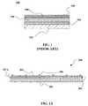
- FIG. 1depicts a schematic diagram of a typical solar cell according to the prior art.
- the solar cell 100generally includes a substrate 102 , a bottom electrode 104 disposed on the substrate 102 , and one or more active layers 106 disposed between the bottom electrode 104 and a top electrode 108 .
- large currentshave to be carried from the PV cell(s) to an outside electrical circuit or device.
- a top surface 109has to be at least semi-transparent to collect this outside light but this light also has to penetrate through the electrode on this side.
- Thisis often achieved by using semi-transparent conducting material in at least one of the top and bottom electrodes 104 , 108 .
- the substrate 102may be transparent or opaque. In cases in which the light of e.g. a PV cell penetrates into the device through the bottom substrate 102 the top electrode 108 does not normally have to be transparent. In cases in which the bottom substrate 102 is opaque the light needs to reach the device (electronically/optically active layer(s)) through the top electrode 108 . Naturally, both the top and bottom electrodes 104 , 108 and the substrate 102 must be at least partly transparent for the case in which the light is desired to reach the active layer(s) 106 from both sides.
- TCEstransparent conducting electrodes
- TCOtransparent conducting oxide
- ITOindium-tin-oxide
- SnO xwith or without fluorine doping
- Al-doped ZnO xetc.
- Such TCO layershave often been combined with metallic grids of additional lower resistance materials, such as e.g. screen-printed metal-particle pastes (e.g. silver-paste).
- screen-printed metal-particle pastese.g. silver-paste.
- U.S. Pat. No. 6,472,594 to Ichinose et aldescribes coating metal with a conductive adhesive in order to attach the wires to and make electrical contact with an underlying TCO.
- Such approachesare still far from optimal as limited light transmission and residual resistances limit device efficiency and manufacturing is costly.
- Such approachesare not compatible with the use of organic PV cells.
- Ichinosein particular does not address applications involving organic PV cells.
- TCO materialsmay not form good ohmic or near-ohmic contacts with organic p-type materials such as those employed in organic or partly-organic solar cells.
- organic or partly organic solar cellsare often more sensitive to ‘process conditions’. For example, depositing a TCO layer (e.g. via the typical sputtering processes or even reactive sputtering processes that create UV and/or plasma conditions) can damage the organic layers such that cells may, for example have electrical shorts.
- any damage and/or surface modification due to the TCO deposition processcan, hence, be relatively much more relevant and damaging in an organic PV cell.
- TCO deposition processestypically employ vacuum-coating steps that are difficult and costly, even in a web-based roll-to-roll process.
- Conductive polymer filmsrepresent an alternative to TCO electrodes.
- Such polymer materialsare far more suitable for roll-to-roll processing, as they can be solution processed/coated.
- such conductive polymer materialsdo not require sputtering or plasma processes to put them on an active layer.
- conductive polymer filmshave sheet resistances significantly higher than TCOs; e.g., about 200 Ohms/square. Because of this, the resistive power loss would be far too high. Thus, pure conductive polymer transparent electrodes are unacceptable for PV approaches.
- an optoelectronic apparatusincludes a transparent conducting electrode having a layer of transparent electrically conducting polymer material and an array of electrically conductive wires distributed across the layer of transparent electrically conducting polymer material.
- the wire array and conducting polymer materialare configured such that the wires are in electrical contact with the polymer material.
- the wireshave small diameters, e.g., typically less than about 200 microns.
- the conductive polymer materialis conductive polythiophene, conductive polyaniline, conductive polypyrroles, PSS-doped PEDOT (e.g. BaytronTM), a derivative of PEDOT, a derivative of polyaniline, a derivative of polypyrrole.
- the conductive polymermay be a conjugated spiro compound, a spiro polymer, a polymer blend or a polymer mixed/doped with other conjugated materials, e.g., dyes.
- the wire arraye.g., in the form of parallel wires or a mesh, may have an open area greater than about 80%.
- the transparent conducting electrodemay also include a thin layer of metal. Such transparent conducting electrodes may be used, e.g., in photovoltaic devices such as solar cells.
- the optoelectronic apparatusmay further comprise an active layer in electrical contact with the transparent conducting electrode.
- the active layermay include two semiconducting materials having different electron affinities, so that the first and second materials have complementary charge transfer properties. The presence of the first and second semiconducting materials may alternate within distances of between about 5 nm and about 100 nm.
- the two semiconducting materialsmay be arrayed using nanostructures such as filled pores, nanolamellas, or matrixed nanostructures.
- the apparatusmay further include a base electrode with the active layer disposed between the base electrode and the transparent conducting electrode.
- a conductive electrodemay be made by distributing an array of conductive wires across a layer of transparent conducting polymer and attaching a transparent conductive polymer layer to the wire array.
- the wires and conductive polymerare attached such that they make electrical contact with each other.
- the wire array and/or conductive polymermay be provided in the form of substantially continuous sheets in a roll-to-roll process.
- Embodiments of the present inventionprovide new and useful electrodes and devices that may be formed relatively inexpensively and on a large scale.
- FIG. 1depicts an optoelectronic device according to the prior art
- FIGS. 2A-2Ddepict cross-sectional schematic diagrams of examples of optoclectronic apparatus that incorporate embodiments of transparent conducting electrodes according to embodiments of the present invention.
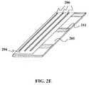
- FIG. 2Edepicts an isometric schematic diagram of an example of an optoelectronic apparatus according to another embodiment of the present invention.
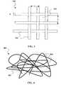
- FIG. 3depicts a diagram of one possible array of wires for a transparent conducting electrode according to an embodiment of the present invention
- FIG. 4depicts a diagram of another possible array of wires for a transparent conducting electrode according to an embodiment of the present invention.
- FIG. 5depicts a cross-sectional schematic diagram illustrating an example of an optoelectronic device according to an embodiment of the present invention.
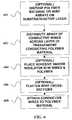
- FIG. 6depicts a flow diagram of a method for making transparent conducting electrodes according to an embodiment of the present invention.
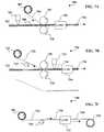
- FIGS. 7A-7Cdepicts schematic diagrams of roll-to-roll processes for producing transparent conducting electrodes according to an embodiment of the present invention.
- FIG. 8depicts a flow diagram of a method for making optoelectronic apparatus and devices according to an embodiment of the present invention.
- FIG. 9depicts an isometric close-up view of a portion of a possible porous film structure.
- FIGS. 10A-10Bdepicts a schematic diagrams of a roll-to-roll processes for making optoelectronic devices according to an embodiment of the present invention.
- DeviceAn assembly or sub-assembly having one or more layers of material.
- semiconductorAs used herein, semiconductor generally refers to a material characterized by an electronic bandgap typically between about 0.5 eV and about 3.5 eV.
- Hole-Acceptor, Electron-AcceptorIn the case of semiconductor materials, hole-acceptor and electron-acceptor are relative terms for describing charge transfer between two materials. For two semiconductor materials wherein a first material has a valence band edge or highest occupied molecular orbital (HOMO) that is higher than the corresponding valence band edge or HOMO for a second material, and wherein the first material has a conduction band edge or lowest unoccupied molecular orbital (LUMO) that is higher than the corresponding conduction band edge or LUMO for the second material, the first material is a hole-acceptor with respect to the second material and the second material is an electron-acceptor with respect to the first material.
- HOMOvalence band edge or highest occupied molecular orbital
- LUMOconduction band edge or lowest unoccupied molecular orbital
- a particular band edge or molecular orbitalis said to be “higher” when it is closer the vacuum level.
- a first and second semiconductor or conductor materialare said to have complementary charge-transfer properties with respect to each other when the first material is a hole-acceptor and/or hole-transporter with respect to the second and the second is an electron-acceptor and/or electron-transporter with respect to the first or vice versa.
- Nano-Architected Porous Filmgenerally refers to a film of material having features characterized by a width, or other characteristic dimension, on the order of several nanometers (10 ⁇ 9 m) across. Nano-architected porous films may be produced by several techniques, including:
- a silica xerogelcan be formed by hydrolysis and polycondensation of silicon alkoxides with organic monomers (e.g. with monomers that are susceptible to polymerization within the porous gel structure).
- organic monomerse.g. with monomers that are susceptible to polymerization within the porous gel structure.
- Methylmethacrylate (MMA)is an example of a suitable organic monomer and the inorganic-organic hybrid obtained after polymerization of the MMA has optical and mechanical properties often superior to the individual components.
- Precursors of this kindhave the formula R x M(OR′) n-x or 3(R′O)Si—R′′—Si(OR′)3, where R and R′ are either hydrogen (H), any organic functional group or a halide, R′′ can be oxygen or an organic functional group, and M is a metal.
- R and R′involve oxygen, e.g., —O—R and — 0 —R′.
- Mmay be any transition metal, e.g., titanium, zinc, zirconium, copper, lanthanum, niobium, strontium, or silicon, etc.
- the hydrolysis of alkoxy groups (OR′) followed by a condensation reactionwill form the mineral network and the R groups will imprint in the network the organic function.
- the pre-formatted species or building blockscould be in this case oxo-metallic clusters, nanoparticles, nano-rods, nano-tubes, nano-whiskers (CdS, CdSe, . . . ), metallic or oxides colloids, organic molecules or oligomers. These blocks are functionalized during or after their synthesis with complementary species for tailoring the interface between organic and inorganic domains.
- (f)Templated growth of inorganic or hybrid networks by using organic molecules and macromolecules as structure directing agents.
- molecules like amines, alkyl ammonium ions, amphiphilic molecules or surfactantscan be used as templates to build a structured mineral network.
- Materials of the zeolites familiesare among the most intensively investigated systems.
- Molecular and supramolecular interactions between template molecules (surfactants, amphiphilic block copolymers, organogelators, etc. . . . ) and the growing hybrid or metal-oxo based networkpermit the construction of complex hybrid hierarchical architectures.
- (g)Templated growth using nanoparticles, as structuring agents followed by removal of the nanoparticles, leaving behind a porous network.
- the nanoparticlesmay be made, e.g., of latex, and removed, e.g., by heating the templated film to a sufficient temperature to “burn off” the nanoparticles.
- Surfactant TemplationIn general, surfactant temptation is a particular subcategory of templated growth. As used herein, surfactant temptation refers an approach toward achieving pore size control of inorganic or organic frameworks, e.g., by using surfactants or block copolymers as templates to build a structured mineral network. Surfactant temptation may be used to prepare a high-porosity surfactant-templated porous thin film. Surfactant temptation includes the sol-gel approach described below.
- Optoelectronic DeviceA device that interacts with radiation and electric current.
- a radiation-emitting devicee.g. a light-emitting diode (LED) or laser
- a radiation absorbing devicee.g. a photodetector/counter, photovoltaic cell (solar cell) or radiation-driven electrolysis cell.
- Solar CellA photovoltaic device that interacts with radiation (often in the form of sunlight) impinging on the device to produce electric power/voltage/current
- Organic Solar CellA type of solar cell wherein an active photoelectric layer is fabricated, either partly or entirely, using organic materials comprising, e.g., polymers, oligomers, molecules, dyes, pigments (including mixtures) that are predominantly carbon based compounds. These materials may be insulating, conductive or semiconductive or mixes thereof.
- RadiationEnergy which may be selectively applied including electromagnetic energy having a wavelength between 10 ⁇ 14 and 10 4 meters including, for example, gamma radiation, x-ray radiation, ultraviolet radiation, visible light, infrared radiation, microwave radiation and radio waves.
- Materialis used herein to refer to solid-state compounds, extended solids, extended solutions, clusters of molecules or atoms, crystals, polymers, dyes, particularly including conjugated polymers and dyes.
- inorganic MaterialsMaterials which do not contain carbon as a principal element.
- the oxides and sulphides of carbon and the metallic carbidesare considered inorganic materials.
- examples of inorganic compoundsinclude, but are not restricted to, the following:
- Intermetallicsconstitute a unique class of metallic materials that form long-range ordered crystal structures below a critical temperature. Such materials form when atoms of two metals combine in certain proportions to form crystals with a different structure from that of either of the two metals (e.g., NiAl, CrBe 2 , CuZn, etc.).
- Metal AlloysA substance having metallic properties and which is composed of a mixture of two or more chemical elements of which at least one is a metal.
- Inorganic polymerssuch as polysilanes or other non-carbon based polymers or monomers.
- a ceramicis a metal oxide, boride, carbide, nitride, or a mixture of such materials.
- examples of such materialsinclude, among others, alumina, zirconia, Titania (TiO 2 ) silicon carbide, aluminum nitride, silicon nitride
- Organic MaterialsCompounds, which principally consist of carbon and hydrogen, with or without oxygen, nitrogen or other elements, except those in which carbon does not play a critical role (e.g., carbonate salts).
- organic materialsthat can be synthesized using the methods of the present invention include, but are not restricted to, the following:
- PolymersMaterials consisting of large macromolecules composed of more than one repeating units. Polymers, composed of 2-8 repeating units are often referred to as oligomers. Examples of such repeating units include, e.g., dyes or pigments. Polymers can be natural or synthetic, cross-linked or non-crosslinked, and they may be homopolymers, copolymers, block-copolymers, or higher-ordered polymers (e.g., terpolymers, etc.). Polymers may be synthesized or grafted onto one another using either classical organic chemistry techniques or using enzymes to catalyze specific reactions.
- polymersinclude, but are not limited to, the following: (polyurethanes, polyesters, polycarbonates, polyethyleneimines, polyacetates, polystyrenes, polyamides,). Although the preceding are examples of electrically insulating polymer materials, some types of polymers may act as semiconducting or conducting materials.
- semiconductive polymerssuch as polyphenylvinylene (and derivatives), polythiophene (and derivatives), polyfluorenes (and derivatives), polyparaphenylene and polymers containing C 60 or dyes such as perylenes or phthalocyanines), conjugated polymers such as polyanilines, polyacetylenes, polypyrroles, and conjugated spiro-compounds, spiro-polymers, polymer blends and polymers mixed/doped with other conjugated materials (e.g. dyes).
- Conjugated polymerssuch as PEDOT (Baytron), polyaniline or polyacetylene may be doped to act as conducting polymers.
- These polymerscan be regular polymers, polymer blends, copolymers (regular or random), block-copolymers (regular or random), side-chain polymers, etc.
- Shadow Lossrefers generally to the losses in photovoltaic efficiency associated with wire mesh transparent electrodes in a photovoltaic cell.
- the wires in the meshtrend to cover an area through which radiation would otherwise pass, thereby reducing the amount of radiation that penetrates to the active layer of the cell.
- Solution processingrefers to forming a film on a substrate by applying a solution (or suspension, dispersion, emulsion; from organic solvents, acidic solutions or water-based solutions) to the substrate with some subsequent drying/baking/cure step in which the solvent(s) is/are removed.
- Embodiments of the electrode of the present inventionis achieved by a combination of a thin-film highly transparent conductive polymer material such as—PEDOT (PEDOT is polyethylene-dioxythiophene doped with polystyrene sulphonic acid (PSS)) or polyaniline (Pani) (typically also doped with e.g. PSS) or doped polypyrroles or any combinations of these or their derivatives and a highly conductive array very fine metal wires with large pitch or a metal mesh with a large ratio of metal to openings. The wires are in electrical contact with the conductive polymer thin-film.
- PEDOTis polyethylene-dioxythiophene doped with polystyrene sulphonic acid (PSS)) or polyaniline (Pani) (typically also doped with e.g. PSS) or doped polypyrroles or any combinations of these or their derivatives
- PSSpolystyrene sulphonic acid
- Panipolyaniline
- the array of metal wiresmay be laminated or ‘woven into’ or extruded into/onto the surface a thin film device (in particular PV cell).
- the metal wiresmay include a conductive epoxy or meltable cladding to provide electrical contact with the conductive polymer material.
- a transparent conductive oxide (TCO)may optionally be disposed over the wires and conductive polymer. The TCO could also be disposed between the wire array/conducting polymer combination and an underlying active layer.
- Transparent conductive electrodes of the type described hereinmay be incorporated into organic PV cells and optoelectronic devices.
- such electrodesmay be incorporated in optoelectronic devices having one or more nanostructured active layers.
- Embodiments of the inventioncan be applied where radiation penetrates the active layer(s) of an optoelectronic device from one side, e.g., through a top electrode or from two sides, e.g., through a top AND a bottom electrode.
- Embodiments of the present inventionhave several advantages over previous transparent electrodes and optoelectronic devices and apparatus. Such advantages include relatively low sheet resistance, relatively low cost and more convenient manufacture compared to prior art transparent electrodes.
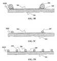
- FIGS. 2A-2Edepicts schematic diagrams of embodiments of an apparatus 200 according to an embodiment of the present invention.
- the apparatus 200generally includes a transparent conducting electrode (TCE) 202 A disposed on an active layer 201 .
- the TCE 202 Agenerally includes an array of metal wires 206 distributed across a layer of transparent conductive polymer 204 The metal wires 206 are in electrical contact with the transparent conductive polymer layer 204 .
- the wire array 206may also be in direct physical contact with the transparent conductive polymer layer 204 .
- the equivalent sheet resistance of the conductive TCE 202is typically less than 100 Ohms/square, preferably less than 10 Ohms/square, more preferably less than 1 Ohms/square and most preferably less than 0.1 Ohms/square.
- the active layer 201interacts with radiation and electric current or voltage. Such an interaction may be a photovoltaic or light-emitting interaction.
- the active layer 201may be a multi-layer structure having two or more sub-layers stacked on top of one another. Alternatively, the presence of two or more materials may alternate with the plane of the active layer.
- the active layer 201may include one or more semiconductor materials.
- active layer 201may include silicon, which may be doped with p-type and/or n-type dopant.
- the siliconmay be crystalline, poly-crystalline or amorphous.
- Other materials suitable for the active layer 201include inorganic semiconductors (crystalline, poly-crystalline or amorphous) such as CdTe, CIGS, etc.
- the active layer 201may be a PV-active layer that converts incident radiant energy to electrical energy.
- the active layer 201could include one or more organic materials (molecules, oligomers, polymers, co-polymers, blends) of one or more layers or phase-separated blends.
- suitable polymersinclude conjugated polymers, (e.g., semiconductive polymers such as polyphenylvinylene, polythiophene, polyfluorenes, polyparaphenylene and polymers containing C 60 or dyes such as perylenes or phthalocyanines) or conductive polymers such as doped PEDOT (Baytron), polyaniline or polyacetylene.
- the active layer 201may include a nano-architected porous film.
- the active layer 201may include a combination of a nanostructured grid of porous inorganic conductive oxide such as, but not exclusively limited, to titania (in its various phases) wherein the pores in the nanostructured grid are filled with combinations of pore-filling materials such as conjugated organic materials (molecules, oligomers, polymers, copolymers, blends, spiro-compounds), organo-metallic sensitizing dyes (such as ruthenium complexes), solid or liquid electrolytes and/or ionic or electronic charge transporting compounds, inorganic semiconductive compounds (e.g. CuO x , CIGS) and the like.
- the porous conductive oxide and the pore filling materialhave complementary charge-transfer properties.
- a negative-charge transporting porous titania gridmay be filled with a positive charge transporting material such as CuO x .
- the transparent conductive polymer layer 204may be made from any of a number of conductive polymers.
- the conductive polymer layer 204is made from conductive polythiophenes, conductive polyanilines or conductive polypyrroles, PSS-doped PEDOT (e.g. BaytronTM), a derivative of PEDOT, a derivative of polyaniline, a derivative of polypyrrole,
- the conductive polymer layeris typically between about 50 nm and about 5000 nm thick, preferably between about 100 nm and about 1000 nm and more preferably between about 100 nm and about 500 nm thick.
- the conductive polymer material for the conductive polymer layer 204is solution-processible. Solution processing is advantageous for several reasons, e.g. in that one can e.g. roll-to-roll-coat the solution (or suspension, dispersion, emulsion, etc.) onto a substrate to form the polymer layer 204 .
- the TCE 202 Amay include an optional first layer 203 (e.g. a very thin metal layer or transparent conductive oxide) may defines the charge injection/extraction efficiency (e.g. via its work-function) and the conductive polymer layer may increase the electrical conductivity of the TCE 202 A and provide electrical contact with the array metal wires 206 .
- the first layer 203may be a transparent conductive oxide (TCO) such as indium-tin-oxide, Al-doped ZnO x , F-doped SnO x , or the like that fills the spaces between the wires 206 .
- TCOtransparent conductive oxide
- the first layer 203may be a very thin layer of a metal or alloy.
- the thin metal or alloy layer used as the first layer 203must be thin enough that it is sufficiently transparent, e.g., less than about 15 nm thick.
- the first layer 203could be a different conductive polymer layer, i.e. different from the transparent conductive polymer layer 204 .
- the first layer 203could be a conductive polymer layer optimized for charge injection/extraction whereas the transparent conductive polymer layer 204 may be optimized for transparency and conductivity and contact with the wire array 206 .
- the TCE 202incorporates an optional first layer 203 , e.g., as a TCO or thin metal (or metal alloy) layer in electrical contact with the conductive polymer layer 204 and/or wire array 206 .
- the wire array 206may be disposed between the first layer 203 and the conductive polymer layer 204 .
- the TCO or thin metal layermay be disposed between the wire array 206 and the conductive polymer layer 204 .
- the conductive polymer layer 204may be disposed between the first layer 203 and the wire array 206 as shown in FIG. 2A. This configuration is especially preferable when using a thin metal or alloy as the first layer 203 .
- the first layermay have either a higher or lower work function than the transparent conducting polymer layer 204 depending on the desired application for the TCE 202 A.
- a higher work function for the first layer 203may be desirable in some applications where the TCE 202 A acts as an anode (i.e., a positive charge carrier collecting electrode for a PV cell or detector or a positive charge injecting electrode for other devices).
- the TCE 202 A acts as a cathodei.e., a negative charge carrier collecting electrode for a PV cell or detector or a negative charge injecting electrode for other devices
- a lower work functionmay be desirable for the first layer 203 .
- the array of wires 206may be placed between the transparent conductive polymer layer 204 and the active layer 201 .
- direct electrical contact between the wires 206 and the active layer 201is undesirable.
- the under-side of the array of wires 206may be partially or fully coated to protect against such undesirable electrical contact.
- FIG. 2Bdepicts a variation on the apparatus 200 in which a TCE 202 B includes a layer of short-proofing material 205 disposed between the wires 206 and active layer 201 .
- the short proofing material 205may be an insulating layer 205 e.g. a plastic, a resin such as an epoxy-resin or an inorganic insulator (oxide, nitride, oxy-nitride, etc.) to protect against such undesirable short circuits.
- the short-proofing material 205may be pre-deposited on the wire 206 or deposited during the lamination process.
- the short-proofing material 205may also be pre-deposited on the active layer 201 before the wire 206 is put down.
- FIG. 2Balso shows that portions of the conductive polymer layer 204 may “creep-up” the sides of the wire 206 , e.g., under the influence of surface tension forces, to provide contact between the wire 206 and the conductive polymer layer 204 .
- the short-proofing material 205may be deposited in a paste or solution/suspension/dispersion form or be laminated (e.g. in the form of a tape).
- the metal wires 206it is desirable for the metal wires 206 to be made from wire material for which an industrially stable supply is available and which may be readily formed into wires or meshes. It is also desirable that the metal composing the metal wires 206 possess a low resistivity, e.g., 10 ⁇ 4 ⁇ cm or less, more preferably below 10 ⁇ 5 Ohm cm.
- a low resistivitye.g. 10 ⁇ 4 ⁇ cm or less, more preferably below 10 ⁇ 5 Ohm cm.
- copper, silver, gold, platinum, aluminum, molybdenum and tungstenare suitable because of their low electric resistance. Of these, copper, silver, and gold are the most desirable due to their low electric resistance.
- the wires 206may be made of aluminum or steel. In particular, Al, Cu, Ag etc have resistivities in the range of around 3 ⁇ 10 ⁇ 6 Ohm cm.
- the wires 206can be made from alloys of two or more metals.
- the wires 206may also be made from a low melting point or reflowable/remeltable low temperature alloy/metal (such as a solder alloy) that can be melted onto or into the underlying conductive polymer layer 204 .
- thin metal layersmay be formed on the surface of the metal wires 206 , e.g., by plating or cladding, for purposes such as corrosion prevention, oxidation prevention, improvement of adhesion, and improvement of electric conductivity.
- precious metalssuch as silver, palladium, silver-palladium alloy, and gold
- other metalssuch as nickel and tin
- gold, silver, and tinoffer good corrosion resistance.
- gold, silver, and tinare not readily affected by moisture, therefore making them suitable for corrosion resistant metal layers. It is also possible to create a coating of conductive resin in which the metals are used as fillers and distributed throughout the resin.
- the wire/meshcould also be pre-coated (before or during the lamination process) with a conductive polymer.
- the thickness of the coatingwill depend on individual preferences, the coating thickness for metal wires with a circular cross section may lie in a range of about 1 % to about 10% of the diameter of the underlying wire.
- the sheet resistance for a TCE the type shown in FIGS. 2A-2Ecan be quite low.
- a TCE using 50-micron diameter Cu or Ag or Al wire with a thread count of one wire per millimeterthis would equate (not counting the much more resistive conductive polymer) to an equivalent sheet resistance of about 0.01 Ohms/square.
- the diameter of the wire 206is chosen to minimize or substantially reduce the effects of electric resistance loss and shadow loss.
- the wires 206desirably have a diameter that is less than about 200 microns and preferably less than about 100 microns and could be less than about 50 microns.
- the percentage of open area (i.e., area not covered by wire 206 ) compared to the wire-covered areais preferably better than about 80%, more preferably higher than about 90% and even more preferably higher than about 95%.
- the cross section of the wire 206can be substantially circular as shown in FIGS. 2A-2B or, as shown in FIG. 2C, wires 207 with cross sections flattened into an oval or elliptical shape may be used in an alternative TCE 202 C.
- the wire 206can have a rectangular, irregular or arbitrary cross-section.
- the wire 206may be brought into contact with the transparent conductive polymer layer 204 by proximity, pressure, heat-treatment (partial or more complete melting or re-flow), or by surface tension forces, etc.
- another alternative TCE 202 Dmay incorporate an adhesive layer 209 between the array of wires 206 and the conductive polymer layer 204 .
- Such an adhesive layer 209could be a conductive paste or epoxy deposited by extrusion, dispensing, spray-coating, printing such as screen-printing, ink-jet printing, flexographic printing, gravure printing, micro-gravure printing, and the like.
- Tape-automated bondingmay also be used.
- the adhesive layer 209could be pre-coated on the wire/mesh (or substrate) or be deposited onto the mesh during the lamination/assembly process e.g. via a roll-to-roll coating technique.
- the adhesive layer 209may be continuous or not.
- the use of certain adhesives in the adhesive layer 209may be incompatible with an organic active layer 201 .
- a high temperature conductive adhesive or meltable or reflowable substancemay melt through and/or into the organic layer(s) and cause damage.
- a short-proofing layer 211may be disposed between the wire 206 and the active layer 201 or pre-patterned on the active layer such that the insulating layer protects the conductive polymer layer 204 while the latter still makes contact between the active layer 201 and the wire 206 .
- the short-proofing layer 211is typically made from an electrically insulating material, e.g., an oxide, glass, or insulating polymer.
- the short-proofing layer 211covers only a small area that provides the direct contact between the wire 206 and the active layer 201 such that the conductive polymer coating 204 still provides sufficient contact from the ‘open areas’ to the wires 206 .
- the adhesive layer 209 described abovecould be used for a conductive adhesive layer as well as an insulating layer between the wire 206 and the active layer 201 .
- the short-proofing layer 211may be in the form of one or more strips of insulating material disposed between the conducting polymer layer 204 and the wire 206 .
- the short-proofing layer 211can also help to protect against shorts between the top and bottom electrodes of an optoelectronic device during a subsequent singulation/cutting/stamping/etc. step, e.g. to create individual sheets of devices originally fabricated in a roll-to-roll process.
- the scope of the present inventionincludes various combinations of the features illustrated in FIGS. 2A-2E. Furthermore, although the first layer 203 (thin metal/alloy or TCO or other conductive polymer) is not shown in FIGS. 2B-2E, such a layer may of course be included in any or all of these variations.
- the wires 206may be in the form of an array of parallel wires that are substantially uniformly spaced apart from each other, as shown in FIG. 2E.
- the wires 206may be arranged in a grid or mesh as shown in FIG. 3.
- a rectangular mesh 300is depicted in FIG. 3, the mesh 300 may have wires 302 arranged in any suitable pattern such as square grid, honey-comb/hexagonal etc.
- the mesh 300may be made of wires of the types described above with respect to FIGS. 2A-2E.
- the wire/meshIn roll-to-roll manufacturing the wire/mesh may be continuous or semi-continuous, may be (if wire form) deposited parallel to the roll-to-roll direction or perpendicular or at an angle in between.
- the wires 302are generally characterized by a diameter d, and are spaced apart to define one or more openings 304 having a characteristic dimension L.
- the characteristic dimension Lmay be a spacing between adjacent wires 302 .
- the number of wires per unit length in the mesh 300may be calculated as 1/L.
- the spacing L between vertical fibersis the same as that for horizontal fibers although the spacings may be different if desired.
- a substantially rectangular web patternis depicted in FIG. 3, other patterns with openings having differently defined characteristic dimensions may be used.
- the wires 302may be woven, knitted or otherwise fashioned into a fabric having useful properties using conventional fabric forming equipment. In the example depicted in FIG. 3, the wires 302 are depicted as being fashioned in a “woven” pattern, wherein fibers running in one direction alternately pass over and under fibers running in a substantially perpendicular direction.
- wires 302may be used when fashioning the mesh 300 .
- a woven meshis undesirable because it provides an uneven surface for adhering the mesh 300 to an underlying layer.
- a fabric-type meshcan have higher and lower points that may increase the risk of shorting during a lamination process.
- the mesh 300may be fabricated or pre-treated so that it is essentially flat on at least one side (that in contact with the active layer or other underlying layer(s).
- the transparency of the resulting web 300depends on the ratio of open area between the wires 302 to the area L 2 , which includes the area covered by the wires 302 .
- the open areacan be determined by subtracting the area covered by the wires 302 (approximately 2dL in this example) from the total area L 2 .
- the open area ratiodepends on the both the fiber spacing L and the fiber diameter d. For the mesh example depicted in FIG. 3, the open area ratio may be given approximately by:
- OPEN AREA RATIO[1-2 d/L ]
- the open area ratiomay be given by:
- OPEN AREA RATIO[1- d/L ]
- a desired open area ratiomay be obtained by fashioning a mesh 300 with an appropriate thread count (1/L)
- the wires 302may be a few tens of microns in diameter and the thread count may be of order 1 wire per mm and the open area ratio may be about 80% or more.
- the array of wires 206may alternatively be fashioned in the form of a web with randomly sized and/or randomly shaped openings.
- FIG. 4depicts a portion of a web 400 with randomly sized and shaped openings 404 may be fashioned from one or more strands of wire 402 , made from an electrically conducting material as described above.
- the wire 402may be placed on a substrate or roller in a random pattern and subjected to pressure, and possibly heat, to compress it into a 2-dimensional or 3-dimensional web 400 . This is a fairly simple process well suited to forming a web 400 from wires 402 that are between a few microns to a few millimeters in diameter.
- the array of wires 206generally lies within a surface that substantially conforms to a surface on which the TCE 202 is disposed.
- the TCE( 202 A, 202 B, 202 C, 202 D, etc.) is disposed on the surface of the active layer 201 , which may be substantially planar.
- the wires 206lie substantially within a plane.
- the TCE 202it is also possible for the TCE 202 to coat an object of arbitrary shape or regular shape, e.g., cylindrical, spherical, etc.
- embodiments of the present inventionare not limited to planar TCE's, planar optoelectronic apparatus, and planar optoelectronic devices.
- Transparent conducting electrodes of the types described above with respect to FIGS. 2A-2E, 3 , and 4may be incorporated into a number of optoelectronic devices.
- Examples of such devicesinclude passive devices such as antistatic films, antireflective stacks, electromagnetic shielding, heat-efficient electrochemical windows, electrochromic windows and electroluminescent lamps. Additional examples include active devices such as flat panel displays (FPD), light emitting diodes and light-sources, laser diodes, transparent membrane switches, touch screens, and solar cells.
- active devicessuch as flat panel displays (FPD), light emitting diodes and light-sources, laser diodes, transparent membrane switches, touch screens, and solar cells.
- Examples of solar cellsinclude thin-film organic, inorganic or hybrid organic/inorganic solar cells as well as conventional non-thin-film solar cells, e.g. based on Si wafers. In each of these types of devices, energy savings can be generated during device operation through the lower resistivity of the transparent conductive electrode.
- an optoelectronic deviceincludes an active layer sandwiched between two electrodes, at least one of which is a transparent conducting electrode having a thin-film highly transparent conductive polymer material and a highly conductive array fine metal wires, as described above.
- FIG. 5depicts an example of a device structure for an optoelectronic device 500 according to an embodiment of the present invention.
- the optoelectronic device 500generally includes an active layer 501 disposed between a transparent conducting electrode (TCE) 502 a base electrode 508 .
- TCEtransparent conducting electrode
- the device 500may be modularized by well-known encapsulation in order to improve weather resistance and mechanical strength e.g., with optional substrate and/or encapsulant layers 510 , 512 .
- the TCE 502has features in common with those described above with respect to FIGS. 2A-2E and FIGS. 4-5.
- the TCE 502generally includes a layer of transparent conductive polymer 504 covered with an array of metal wires 506 .
- the layer of transparent conductive polymermay 504 be, e.g., a layer of PEDOT or any of the other polymer materials described above.
- the array of wires 506may be in the form of a fine copper mesh having wires about 50 ⁇ m in diameter and an open area of about 79%.
- the wires 506may have a circular cross-section or a flattened cross-section as described above with respect to FIG. 2C.
- the lateral spaces between the wires 506may be filled with a transparent material 503 .
- suitable transparent material 503include clear thermoplastic materials.
- the transparent material 503could be used to glue the whole underlying structure to the encapsulation sheet 512 to the TCE 502 .
- the transparent material 503may include a transparent conducting oxide (TCO) that his been deposited over the wires 506 and conductive polymer material 504 .
- TCOtransparent conducting oxide
- the TCOmay not fill the whole space between the wires 506 , polymer 504 and encapsulant 512 . In such a case, the remainder of the space may be filled with a clear glue or other fill material.
- the TCE 502may optionally include an insulator layer as described above with respect to FIGS. 2B and/or 2 E or an adhesion layer as described above with respect to FIG. 2D.
- the base electrode 508may optionally be a TCE, e.g., of the type described above. Whether the base electrode 508 is transparent or not depends partly on the nature of the device 500 . For example, if the device 500 is a window (e.g., an electrochemical or electrochromic window) both electrodes 502 , 510 need to be transparent. On the other hand for radiation emitting devices such as LED's or laser diodes or radiation absorbing devices such as PV cells the base electrode 508 need not be transparent.
- the base electrode 508may be in the form of a commercially available sheet material such as such as C-, Au-, Ag-, Al-, or Cu-coated Steel Foil or metal/alloy-coated plastic foils, including metal or metallised plastic substrates/foils that are planarized to reduce surface roughness.
- a commercially available sheet materialsuch as C-, Au-, Ag-, Al-, or Cu-coated Steel Foil or metal/alloy-coated plastic foils, including metal or metallised plastic substrates/foils that are planarized to reduce surface roughness.
- the active layer 501may include a single layer of material or multiple layers.
- the active layer 501may generate, absorb, or transmit radiation that passes through the transparent electrode 502 .
- the active layermay comprise a polymer electrolyte disposed between a layer of vanadium pentoxide and a layer of tungsten oxide. The passage of a small current between the electrodes 502 , 508 changes the tungsten oxide from transparent to substantially opaque.
- the active layer 504may include a liquid crystal layer disposed between to alignment layers. Such structures may be used, e.g. in liquid crystal displays.
- the active layer 501may be in the form of an exciton-splitting and charge transporting network.
- an exciton-splitting networktypically includes two complementary semiconductor materials.
- the two semiconducting materialswill have different electron affinities. Interaction between radiation and charge occurs in the vicinity of an interface between the two different materials in the active layer 501 .
- the two complementary semiconductor materialsmay be in the form of a nanoscale grid network 505 and a network-filling material 507 .
- two semiconducting materialsmay be regularly arrayed such that presence of the two semiconducting materials alternates within distances of between about 5 nm and about 100 nm.
- the active layer 501may include an optional first interface layer 509 that contacts the TCE 502 .
- One function of the first interface layer 509is to avoid e.g. shorts between the TCE 502 and the nanoscale grid network 505 .
- the interface layer 509may also include a metal or alloy layer having a lower work-function than the TCE 502 as described above with respect to the first layer 203 of FIG. 2A.
- the first interface layer 509may also improve mechanical properties such as flexibility.
- the active layer 501may also include a second optional interface layer 511 that contacts the base electrode 508 .
- the second interface layer 511may inhibit electrical shorts between the base electrode 508 and the network filling material 507 .
- the second interface layermay optionally include a metal or alloy layer with a lower work-function than the base electrode 508 .
- the nanoscale grid network 505 and network filling material 507are shown in simplified form for the sake of clarity.
- the structures in the grid network 505may be aligned substantially parallel to each other as shown in FIG. 5, the structures may also be interconnected and, most importantly, accessible from both neighboring layers, e.g. electrodes 502 , 508 or interface layers 509 , 511 .
- One possible variation, among others, of a possible configuration of the structures in a nanoscale grid networkis that shown in FIG. 9.
- a nanostructured active layer 501is depicted in FIG. 5, the active layer 501 may alternatively be of conventional design.
- the nanoscale grid network 505may contain substantially uniformly distributed, e.g., regularly spaced, structures roughly 1 nm to 100 nm in diameter and more preferably, about 5 nm to about 25 nm in diameter.
- neighboring structuresare between about 1 nm and about 100 nm apart, measured, e.g., from nearest edge to nearest edge. More preferably, the pores are between about 5 nm apart and 25 nm apart, edge to edge.
- the nanoscale grid network 505may be made from an electron-accepting material, e.g., Titania, (TiO 2 ) zinc oxide (ZnO 2 ), zirconium oxide, lanthanum oxide, niobium oxide, aluminum oxide, tungsten oxide, strontium oxide, calcium/titanium oxide, sodium titanate, potassium niobate, Cadmium Selenide (CdSe), Cadmium Sulfide (CdS), or Cadmium Telluride (CdTe) as well as blends of two or more such materials such as TiO 2 /SiO 2 blends/hybrids.
- an electron-accepting materiale.g., Titania, (TiO 2 ) zinc oxide (ZnO 2 ), zirconium oxide, lanthanum oxide, niobium oxide, aluminum oxide, tungsten oxide, strontium oxide, calcium/titanium oxide, sodium titanate, potassium niobate, Cadmium Sel
- the network filling materialmay be made from a hole accepting material.
- the first optional interface layer 509may inhibit or prevent direct contact between the nanoscale grid network 505 and the transparent electrode 502 .
- the first interface layer 509may be made from the same material as the network filling material 507 .
- the network-filling material 507fills the spaces between the structures in the nanoscale grid network 505 .
- the spaces between the structuresmay be in the form of pores in layer of porous material.
- the spaces between the structuresmay be gaps left behind when pores in a porous material have been filled with a pore-filling material and the porous material etched away leaving behind structures made from the pore-filling material.
- the second optional interface layer 511may inhibit or prevent direct contact between the network filling material and the base electrode 508 .
- the second interface layer 511may be made from the same material as the nanoscale grid network 505 .
- the network-filling material 507is a complementary, i.e., hole-accepting and hole-transporting, organic semiconducting material.
- suitable semiconducting organic materialsinclude those set forth above with respect to the active layer 201 .
- the optional encapsulants 510 , 512protect the device 500 from the surrounding environment.
- the encapsulants 510 , 512may also absorb UV-light to protect organic materials disposed between the encapsulants 510 , 512 .
- suitable encapsulant materialsinclude one or more layers of glass or polymers, such as polyethylene terephthalate (PET) and/or Mylar®.
- PETpolyethylene terephthalate
- Mylaris a registered trademark of E. I. du Pont de Nemours and Company of Wilmington, Del.
- Either encapsulant layers 510 , 512may include EVA (ethylene vinyl acetate), which has favorable adhesive, weather resistance, and buffer effect properties.
- a fluorine resinmay laminated the encapsulant layers 510 , 512 as a surface protecting layer.
- tetra-fluoro ethylene copolymer(TFE, Du Pont TEFLON), copolymer of tetra-fluoroethylene and ethylene (ETFE, Du Pont TEFZEL), polyvinyl fluoride (Du Pont TEDLAR), polychlorofluoroethylene (CTFEC, Daikin Industries Neoflon) are cited.
- Weather resistancecan also be improved by adding a well-known UV absorber.
- the encapsulants 510 , 512may also include nitrides, oxides, oxynitrides or other inorganic materials that protect against exposure to water or air.
- the encapsulantmay be a multi-layer stack or a foil comprising a multi-layer stack of organic materials with inorganic dielectrics.
- Transparent conducting electrodes, apparatus and devices of the types described abovemay be manufactured in accordance with an inventive method.
- An example of a method 600 for fabricating a transparent conducing electrodeis illustrated generally by the flow diagram of FIG. 6 and the schematic diagrains shown in FIG. 7A and FIG. 7B.
- the method 600begins at 602 by distributing an array of conductive wires across a layer of transparent conducting polymer material.
- adhesives and/or insulating materialmay optionally be placed between the wires and polymer material as described with respect to FIGS. 2B and 2D.
- the cross-sections of the wiresmay be flattened as described above with respect to FIG. 2C.
- this flatteningis done prior to any lamination of the wire array to the transparent conductive polymer layer.
- the conductive wiresare attached to the layer of conductive polymer material to form a transparent conducting electrode.
- the attaching process in 608is such that the conductive wires are brought into electrical contact with the layer of transparent conducting polymer material to produce a transparent conductive electrode.
- the order of the stepsdepends on the nature of the fabrication process. Some of the steps may occur sequentially, others may occur simultaneously.
- the wires or the polymer materialare first disposed on an underlying sheet, e.g., a substrate or active layer at step 601 .
- the underlying sheetmay be a partially fabricated optoelectronic device, e.g., like the device 500 of FIG. 5 with all layers up to the first interface layer 509 .
- the conducting polymer materialmay be formed on the sheet first, e.g., by applying a solution or suspension to the sheet.
- the wiresmay be embedded in the wet solution and the solution may be cured.
- the wiresmay be disposed on the sheet first and the solution disposed over the wires at and then cured at step 602 .
- FIG. 7Adepicts a schematic diagram of an embodiment of one possible apparatus 700 for forming a TCE on an underlying sheet.
- a dispenser 703applies a process solution 704 to an underlying sheet 702 .
- the sheet 702may be a substrate material or a partially completed optoelectronic device sheet.
- a roll 705supplies a wire array 706 .
- Rollers 707 , 708laminate (with or without the application of pressure) the wire array 706 into the wet solution 704 .
- the sheet 702carries the solution 704 and wire array 706 to a curing unit 709 .
- the curing unit 709dries, heats, and/or irradiates the solution 704 to set it into a transparent conducting polymer to form a TCE 710 attached to the underlying sheet 702 .
- the sheet 702 with the attached TCE 710may then be encapsulated and/or cut into smaller individual sections.
- the apparatus 700may optionally include a deposition stage for depositing a TCO, thin metal layer or second layer of conductive polymer.
- Such a deposition stagemay implement sputtering or electron beam evaporation or the like for TCO deposition or thermal/resistive evaporation, electron beam evaporation, ion plating, sputtering and the like for thin metal layer deposition.
- the TCO or thin metal layermay be deposited on the sheet 702 before applying the process solution 704 or on the TCE 710 after curing the process solution 704 .
- a second conductive polymer layermay be deposited on the underlying sheet 702 , e.g., from a process solution or dry coating process, before depositing the process solution 704 and/or wire array 706 .
- FIG. 7Bdepicts an alternative apparatus 720 , which is a variation on the apparatus 700 .
- the apparatus 720forms a TCE 738 attached to an underlying sheet 722 such as a substrate or partially completed device.
- a roll 724provides a wire array 726 .
- An applicator 727e.g., a roller
- rollers 728 , 730laminate (with or without the application of pressure and/or heat) the wire array to the sheet 722 .
- An applicator 732then applies a process solution 734 to the wire array 726 and through spaces between the wires in the array to the sheet 722 .
- a curing unit 736then cures the process solution 734 to form a transparent conductive polymer layer.
- the conductive polymer layer and the wire array 726form the TCE 738 attached to the underlying sheet 722 .
- the sheet 722 with the attached TCE 738may then be encapsulated and/or cut into smaller individual sections.
- the apparatus 720may also include a stage (not shown) for depositing (e.g., sputtering) a TCO or thin metal layer on the sheet 722 before or after attaching the wire array 726 or after curing the process solution 734 .
- the applicator roller 727may apply a second conductive polymer layer to the underside of the wire array 726 .
- a conductive polymer coating layer(as additional option on top of the adhesive and/or insulating layers discussed earlier) could provide an effective conductive ‘glue’ with little or reduced risk of causing damage to the underlying active layer(s) by the wire lamination.
- Processing of the type depicted in FIG. 7A and FIG. 7Bis particularly advantageous because of the economies of scale associated with roll-to-roll production.
- the fabrication schemes depicted in FIG. 7A and 7Bare particularly advantageous when using solution processing. Both schemes allow the TCE to be baked to remove solvents prior to encapsulation or lamination of other layers on top of the TCE.
- the transparent electrode described hereinfacilitates the ‘rolling-up’ (e.g. for temporary storage, curing, baking, transport, etc.) of the laminate whereby the wire array 706 provide a spacer and protection for the active device during and in the ‘rolled-up’ state.
- transparent conducting electrodes of the type described abovemay be manufactured by a roll-to-roll process without an underlying sheet. e.g., by coating a mesh foil with a transparent conductive polymer.
- FIG. 7Cschematically illustrates roll-to-roll processing to produce a transparent conducting electrode of the type described above.
- a feeder roll 742provides an array of conductive wire 744 , preferably in the form of a regular screen, mesh, grid or the like.
- An applicator roller 745may apply a process solution 746 the wire array 744 that will form a transparent conductive polymer material to implement the features described above with respect to FIG. 2B and/or FIG. 2D. After the process solution 746 is applied, the wire array 744 may pass through a curing stage 747 . Prior to the applicator roller 745 , the wire array 744 may also pass between an optional pair of compression rollers (not shown) to provide the wires 744 with flattened cross-sections as described with respect to FIG. 2C.
- the curing stage 747may apply some combination of heat, drying and/or radiation to the polymer process solution 746 and/or wire arrays 744 .
- the curing processattaches the wire array to the transparent conductive polymer layer to from a transparent conductive electrode sheet 748 .
- a take-up roller 750may then collect the transparent conductive electrode sheet 748 .
- the transparent conductive electrode sheet 748may move to a further processing stage in which it may be laminated directly to a substrate and/or other parts of a semi-finished device.
- FIGS. 7A-7COther alternative fabrication schemes may combine various features described above with respect to FIGS. 7A-7C. Such alternatives include (a) doing all the fabrication steps on a sheet basis and (b) doing some steps on a sheet basis (e.g. up to layer 502 in FIG. 5) on a roll-to-roll and doing the final lamination to a sheet encapsulation layer ( 512 in FIG. 5) after ‘singulation’ of the roll (i.e., after forming the TCE and/or device into a single sheet).
- a sheet basise.g. up to layer 502 in FIG. 5
- a sheet encapsulation layer512 in FIG. 5
- ‘singulation’ of the rolli.e., after forming the TCE and/or device into a single sheet.
- FIG. 8depicts a flow diagram of a method 800 for fabricating an apparatus of the type shown in FIGS. 2A-2E and optionally incorporating such an apparatus into a device of the type shown in FIG. 5.
- the method 800begins at 802 by providing a TCE having an array of conductive wires distributed across and in electrical contact with a layer of transparent conducting polymer material.
- an active layeris disposed in electrical contact with the TCE. This step may involve bringing the TCE and active layer into close proximity or physical contact. This step may also involve disposing an interface layer between the TCE and active layer. In the most likely scenario, is to start out with a substrate foil; form the active layer on the substrate foil at 804 and then form the TCE at 802 . This could all be done in one continuous process.
- an optional insulator materialmay be disposed between the active layer and either the wires or polymer layer of the transparent conductive electrode as described with respect to FIG. 2E. As a practical matter, this step may occur before step 804 by attaching the insulator material to the polymer layer or wires. Alternatively, the insulating material may be disposed in a pattern on the active layer.
- the active layeris attached to the TCE to form the optoelectronic apparatus.
- the attachment processmakes a mechanical attachment between the TCE and the active layer.
- the active layermay include organic and/or nanostructured semiconductor materials as described below.
- the attaching processmay be part of the process by which the conductive wires are brought into electrical contact with the layer of transparent conducting polymer material to produce the TCE.
- the active layermay be disposed between the TCE and an optional base electrode and the base electrode is attached to the active layer to form the device.
- the base electrodeis attached to the free surface of the active layer (i.e., the surface to which the transparent conductive electrode is not attached).
- the base electrodemay be attached to the active layer either before, after or concurrent with attaching the TCE to the active layer.
- the devicemay optionally be encapsulated at 812 . Again, the most likely scenario is: substrate then base electrode then active layer then TCE.
- the active layer 501may be built on the base electrode 508 and the transparent conducing electrode 502 may be separately fabricated as described above with respect to FIG. 6.
- the transparent conducting electrode 502 and the active layer 501may then be laminated together to complete the apparatus or device.
- the base electrode 508may then be laminated to the exposed surface of the active layer 501 .
- the encapsulant layers 510 , 512may be laminated to the rest of the device 500 e.g., by heating and compression in a vacuum.
- a commercially available device, such as a vacuum laminator, for example,can be used.
- the preferred assembly sequenceis as follows: First the base electrode 508 is attached to the substrate (e.g., encapsulant layer 510 ; then the active layer 501 is built up from the base electrode then the TCE 502 is formed on the active layer 501 , e.g., as described with respect to FIG. 7A or FIG. 7B; finally, the encapsulant layer 512 is applied to the TCE.
- the substratee.g., encapsulant layer 510
- the active layer 501is built up from the base electrode
- the TCE 502is formed on the active layer 501 , e.g., as described with respect to FIG. 7A or FIG. 7B
- the encapsulant layer 512is applied to the TCE.
- the device 500may be constructed as follows.
- a commercially available sheet materialsuch as such as C- or Cu-coated steel foil is used as a base for the device and the base electrode 508 .
- a coating of a sol-gel based non-porous Titania filmbe disposed on the sheet material as the interface layer 511 .
- the nanoscale grid network 505may be a nanostructured porous Titania film formed on the interface layer 511 .
- the porous titania filmis dried and pores in the film are then filled with a hole accepting polymer such as polythiophene as the network filling material 507 .
- the nanostructured porous titania film and hole-accepting polymercreate a nanoscale, high-interfacial area charge-splitting and transporting network.
- a second, flat coating of polythiopheneis then applied as the interface layer 509 , followed by a layer of PEDOT, a transparent conducting polymer 504 .
- the wire array 502a fine copper mesh (50 ⁇ m wire diameter, 79% open area), is applied on top of the PEDOT. Lateral spaces between the wires 502 are filled with a clear thermoplastic material, , which serves as the transparent material 503 .
- Thin glass encapsulating layers 510 , 512may then be laminated to the device 500 .
- One approach, among othersis simply to dispose a two-layer structure between the base electrode and the transparent conducting electrode.
- the two-layer structureincludes two semiconducting or conducting charge transfer layers having complementary charge transfer properties with respect to each other.
- Such an approachmay be extended to active layers having more than two semiconducting or conducting layers.
- charge transfer layersmay be layers of different conjugated polymers that are laminated to each other to form the active layer.
- a single layer of a blend or mixture of organic or organic and inorganic materialsmay be applied, for example a polymer blend or a polymer inorganic nano-crystal mixture.
- Such an active layermay be subsequently or simultaneously laminated between the TCE and base electrode to form the device.
- the two layers forming the active layermay be deposited on a sheet of base electrode material or the conductive polymer layer of the TCE, e.g., by spray coating, printing such as screen-printing, ink-jet printing, flexographic printing, gravure printing, micro-gravure printing, or the like, web coating, doctor blade coating, spin coating or dip coating.
- nano-architected porous filmsAnother approach to forming the active layer involves forming a nano-architected porous film.
- techniques for forming nano-architected porous filmsinclude (a) Intercalation and/or grafting of organic or polymeric molecules within a mineral lamellar network comprised, e.g., of clays, phosphates, phosphonates, etc.; (b) synthesis by electrocrystallisation of hybrid molecular assemblies; (c) impregnation of preformed inorganic gels; (d) synthesis from heterofunctional metallic alkoxides metallic halides or silsesquioxannes; (e) synthesis of hybrid networks through the connection of well-defined functional nanobuilding blocks; (f) Templated growth of inorganic or hybrid networks by using organic molecules and macromolecules as structure directing agents; and (g)
- FIG. 9depicts a simplified and somewhat idealized diagram of a desirable morphology for the nano-architected porous film 900 having numerous pores 901 that are interconnected with each other.
- the poresrun along x, y and z directions and intersect with each other as shown in the inset in FIG. 9.
- the pores 901provide continuous paths between opposite surfaces of the nano-architected porous film 900 .
- the path through the pores 901provides access to the pores from a layer overlying or a layer underlying the surfactant-templated porous film 900 .
- chargeshave a path to migrate through the pore filling material from the overlying layer to the underlying layer and/or vice versa.
- a nano-architected porous filmmay be fabricated by surfactant temptation using a precursor sol containing a mixture of one or more alkoxides, one or more surfactants one or more condensation inhibitors, water, and ethanol.
- suitable alkoxides where the central element in the alkoxides is silicon (Si)include polysiloxanes such as tetraethylorthosilicate (TEOS).
- the central element or inorganic network atom in the alkoxidemay be e.g., Ag, Al, Au, B, Ba, Cd, Co, Cu, Fe, Tr, Mo, Nb, Ni, Pb, Se, Si, Sn, Sr, Ti, V, W, Y, Zn, Zr, etc.
- Suitable surfactantsinclude compounds of the type: HO(CH 2 CH 2 O) n (CH 2 CHCH 3 O) m (CH 2 CH 2 O) n H, where the subscripts m and n are integers.
- a particular surfactant of this typeis the block copolymer poly(ethyleneoxide)-b-poly(propyleneoxide)-b-poly(ethyleneoxide) (EO20-PO70EO20), sometimes known commercially as Pluronic P123.
- Pluronicis a registered trademark of BASF Corporation of Ludwigshafen, Germany.
- Other suitable surfactantsinclude hexadecyl trimethylammonium bromide (CTAB), polyoxyalkylene ether (e.g. Pluronic F127), and poly(oxyethylene) cetyl ether (e.g., Brij56 or Brij58). Brij is a registered trademark of Atlas Chemicals of Wilmington Del.
- condensation inhibitorsinclude acids such as hydrochloric acid (HCl), sulfuric acid (H 2 SO 4 ), nitric acid (HNO 3 ), etc., bases such as sodium hydroxide (NaOH), triethylamine, etc., and chelating agents, including acetyl acetone, alcohol amines, peroxides, etc.
- acidssuch as hydrochloric acid (HCl), sulfuric acid (H 2 SO 4 ), nitric acid (HNO 3 ), etc.
- basessuch as sodium hydroxide (NaOH), triethylamine, etc.
- chelating agentsincluding acetyl acetone, alcohol amines, peroxides, etc.
- a thin filmmay be prepared from the sol by spin-coating, web-coating, dip-coating, spray-coating, printing such as screen-printing, ink-jet printing, flexographic printing, gravure printing, micro-gravure printing, etc. onto a substrate.
- evaporation of the solventcauses the formation of surfactant-stabilized polypropylene microemulsions incorporated into a surfactant-templated material, which can be permanently fixed by annealing through exposure to heat and/or radiation. The annealing preferably occurs before the deposition of any material into the porous template film. Formation of nanostructured porous films is described in greater detail in commonly assigned U.S. patent applications Ser. Nos. 10/290,119, 10/303,665, 10/319,406 and 10/338,079, all of which have been incorporated herein by reference.
- the pores within the nano-architected porous films described abovemay be substantially filled with a conducting or semiconducting material having complementary charge transfer properties with respect to the material of the nano-architected porous film.
- suitable materialsinclude those described above with respect to the active layers in FIGS. 2A-2E and FIG. 5.
- Techniquessuch as web coating, spray coating, spin coating, printing such as screen-printing, ink-jet printing, flexographic printing, gravure printing, micro-gravure printing, or the like, doctor blade coating, dip-coating, and the like may be used to deposit the material that fills the pores in the nano-architected film.
- the same techniquesmay be used to fill the spaces in a network grid where the nano-architected porous film has been etched away after filling the pores.
- Thisis a desirable scheme where, e.g., either the network grid, the network-filling material, or both are to be made from organic materials such as conjugated polymers.
- the porescan be substantially filled by electrochemically growing metal or semiconductor within the pore channels of the nano-architected porous film.
- electrodepositioneither the base electrode or the TCE may serve as a working electrode, which serves to attract ions from a solution and thus drive the formation of material within the pores.
- FIG. 10Adepicts a schematic diagram of a preferred example, of the use of roll-to-roll processing to produce apparatus of the types shown in FIGS. 2A-2E and devices of the type shown in FIG. 5.
- arrowsindicate the directions of travel of sheet material and the directions of rotation of rollers. The number and configuration of the rollers in FIG. 10A has been simplified for the sake of clarity.
- a feeder roller 1001supplies base electrode material 1002 that is attached to a substrate 1003 .
- the feeder roller 1001may supply a substrate 1003 with the base electrode material 1002 already attached.
- the base electrode material 1002may be in the form of a commercially available sheet material such as copper, stainless steel or aluminum foil, metalized plastic foils, foils with transparent electrodes such as TCOs or conductive polymers with or without additional resistance-lowering metal traces that could be pre-deposited/patterned onto the substrate. Note that such polymer/metal or TCO/metal traces can be produced using means other than described herein (e.g.
- the base electrode material 1002 materialmay be a completed transparent conducting electrode sheet, manufactured, e.g., as described above with respect to FIGS. 7A-7C.
- the substrate 1003may be a glass or polymer material, which can serve as an encapsulant for the completed device.
- the substrate 1003 and base electrode material 1002may be provide as a single sheet, e.g., a sheet/foil/roll with a pre-deposited base electrode (metal, TCO etc.).
- a conveyor belt (or a series of conveyor belts) or the likemay carry the substrate 1003 through the subsequent stages of the apparatus 1000 .
- the substrate 1003carries the electrode material 1002 past one or more dispensers, e.g., first and second dispensers 1004 , 1006 .
- the dispensers 1004 , 1006dispense materials that will form an interface layer 1005 and a nanostructured porous layer 1009 .
- the dispensers 1004 , 1006may be conventional rollers, spray coaters, meniscus coater, bar-coater, gravure coater, Mayer rod, doctor blade, extrusion, micro-gravure, web coaters, doctor blade coaters, in-line printers (as above: screen, flexo, etc.)
- the materials that form the interface layer 1005 and nanostructured porous layer 1009may be in the form of liquids (solutions, dispersions, emulsions, suspensions, etc) which may be applied by well-known web-coating techniques and the like.
- the first dispenser 1004may deposit the interface layer 1005 as a substantially continuous layer of semiconducting material, such as TiO 2 .
- a subsequent annealing stage(not shown) to anneal or otherwise process the interface layer 1005 , e.g., by heating, exposure to radiation, a corona discharge or a plasma or some combination of these.
- the second dispenser 1006then applies a precursor sol 1007 that will become the nanostructured porous layer 1009 . Examples of precursor sols are described above.
- the sheet material 1003then passes though an annealing stage 1008 to process the precursor sol 1007 into the nanostructured porous layer 1009 .
- the annealing stage 1008may subject the precursor sol 1007 to heat irradiation corona discharge, plasma (also as above) to provide the desired level of cross-linking.
- a third dispenser 1010provides pore-filling material that fills the pores in the nanostructured porous layer 1009 to form a nanostructured active layer 1011 .
- the third dispenser 1010may be a web-coater, doctor blade coater, spray coater, or a printer such as printing such as screen-printer, ink-jet printer, flexographic printer, gravure printer, micro-gravure printer, etc.
- the substrate 1003may pass through a curing unit (not shown) to evaporate solvents and set the pore-filling material and/or to assist material infiltration, e.g., through capillary action.
- Additional dispensers (not shown) or the third dispenser 1010may deposit additional material onto the active layer 1011 to form a second interface layer as described above with respect to FIG. 5.
- An additional curing stage(not shown) may set and cure the interface layer.
- a TCE 1019may be formed on top of the active layer in the manner described above with respect to FIG. 7A, 7B, or 7 C.
- a fourth dispenser 1012applies to the active layer 1011 a process solution 1013 for forming a layer of transparent conducting polymer material.
- a feeder roller 1014supplies a wire array 1015 that is laminated (with or without pressure) into the process solution 1013 , e.g., by rollers 1016 , 1017 .
- the wire array 1015may pass between an optional pair of compression rollers (not shown) to flatten the cross-sections of the wires.
- the substrate 1003passes through a curing unit 1018 that evaporates solvent from the process solution 1013 and cures the process solution to attach the wire array 1015 to the layer of transparent conductive polymer to form the TCE 1019 .
- the TCE 1019may alternatively be formed as shown in FIG. 7B, i.e., by adhering the wire array 1015 to the device layer first; applying the process solution 1013 over the active layer 1011 and the wire array 1015 ; and then curing in the curing unit 1018 .
- the devicemay be encapsulated.
- an encapsulation unit 1020may laminate an encapsulant layer 1021 over the TCE 1019 to from a completed device sheet 1022 .
- the device sheet 1022may be cut into smaller sections after encapsulation.
- the substrate 1003may be cut into smaller sections at an earlier stage in the processing depicted in FIG. 10A.
- the device sheet 1022is shown as being built up from a substrate 1003 it is also possible to build the device sheet up starting from the base electrode sheet 1002 ; then build the active layer 1011 and TCE 1019 ; and then add encapsulant layers over both the base electrode 1002 and TCE 1019 .
- Another variation of the process described with respect to FIG. 10Ais to fabricate the active layer 1011 using two organic semiconducting materials.
- organic semiconducting materialsmay be deposited on the base electrode 1002 in either single or multi-layers, with or without blends, etc.).
- the use of two organic semiconductor materials, e.g. polymerscan make the active layer 1011 more flexible.
- the substrate 1003is made from a flexible material, e.g., a polymer
- the unencapsulated device sheetcan be rolled up into a roll after forming the TCE 1019 .
- flexible materialssuch as Mylar (e.g. with one or more dielectric barrier layers) are used as the encapsulant layer 1021 , then the encapsulated device sheet 1022 may be rolled up into a roll.
- active layer 1011may be formed as a hybrid organic/inorganic layer as follows.
- the pores in the nanostructured porous layer 1009may be filled with an inorganic material, e.g., by electrodeposition. After filling the pores and before forming TCE 1019 , the nanostructured porous layer 1009 may be etched away and the spaces left behind may be filled with an organic semiconductor having complementary charge-transfer properties with respect to the material that filled the pores.
- FIG. 10Bdepicts a roll-to-roll apparatus that incorporates features from FIG. 7C and FIG. 10A.
- the roll-to-roll apparatus 1030includes a TCE-making section 1031 and an active-layer-making section 1051 .
- a feeder roll 1032provides arrays of conductive wire 1034 .
- An optional applicator roller 1035may apply a polymer process solution that will form a layer of transparent conducting polymer.
- the applicator roller 1035(or a different one) may also apply an adhesive and/or insulating material to the side of wire arrays 1034 to implement the features described above with respect to FIG. 2B and/or FIG. 2D.
- the wire arrays 1034may pass between an optional pair of compression rollers (not shown) to flatten the cross-sections of the wires in the wire arrays 1034 .
- the wire arrays 1034 and process solution 1036pass through a curing unit 1038 , as described above, to set the process solution into the transparent conductive polymer to form a transparent conducting electrode sheet 1040 .
- the active-layer-making section 1051operates substantially as described above with respect to FIG. 10A.
- a feeder roll 1052supplies base electrode material 1054
- One or more dispensers 1055 , 1056dispense materials for forming an interface layer 1057 and a nanostuctured porous layer 1059 .
- a first dispenser 1055may deposit the interface layer 1057 as a substantially continuous layer of semiconducting material, such as TiO 2
- the electrode material 1054may pass through an annealing stage (not shown) to anneal or otherwise process the interface layer 1057 .
- the base electrode material 1054then passes a second dispenser 1056 , which dispenses a precursor sol 1058 for forming the nanostructured porous layer 1059 .
- the base electrode material 1054next passes through an annealing stage 1060 to process the precursor sol 1058 into the nanostructured porous layer 1059 as described above.
- a third dispenser 1061provides pore-filling material that fills the pores in the nanostructured porous layer 1059 to form a nanostructured active layer 1052 .
- the base electrode material 1054may pass through a curing unit (not shown) to evaporate solvents and set the pore-filling material.
- the third 1062 dispenseris depicted as being a roller-based dispenser.
- the transparent conductive electrode sheet 1040 and the base electrode sheet 1054are laminated or otherwise attached to each other with the active layer 1062 disposed between them, e.g., by some combination of heat and compression between a pair of rollers 1064 , 1065 .
- An optional second interface layermay be disposed between the nanostructured active layer and the conductive transparent electrode 1054 before laminating the transparent conductive electrode sheet 1054 and the base electrode sheet 1054 to form a device sheet 1066 .
- the interface layer materiale.g., the same type of material used as the pore-filling material, may be applied to the exposed surface of the nanostructured active layer 1062 .
- the interface layer materialmay be applied to an exposed surface of the transparent conductive electrode 1064 , e.g., the conductive polymer layer 1036 . It is also possible to apply the interface layer material to both the exposed surface of the nanostructured active layer 1062 and the transparent conductive electrode sheet 1040 .
- encapsulant layers 1068 , 1069may be attached to opposite sides of the device sheet 1066 e.g., by heating and compression in a vacuum to form an encapsulated device sheet 1070 .
- a commercially available devicesuch as a vacuum laminator, for example, can be used for this stage of processing.
- the device sheet 1066may be cut into individual optoelectronic devices and then encapsulated or encapsulated first and later cut into individual optoelectronic devices.
- FIGS. 10A-10Bdepicts but two possible roll-to-roll processing schemes. Other variations on these schemes are within the scope of the present invention.
- the active layers 1011 , 1062may be built up from a transparent conductive electrode instead of a base electrode.
- One way to do thisis to start with a prefabricated conductive electrode on the feeder rollers 1001 , 1052 in the place of the base electrode sheets 1002 , 1054 . Note that in this represents one way of producing an optoelectronic apparatus of the type described with respect to FIGS. 2A-2D.
- additional feeder rollers or metal deposition apparatusmay be integrated into the roll-to-roll apparatus 1000 or 1030 to provide a thin metal layer for the TCEs 1019 , 1040 .
- the transparent conductive electrode 1040may be prefabricated into a roll, e.g., as shown in FIG. 7C, prior to processing in the roll-to-roll apparatus 1030 .
- the TCE-making section 1031may be replaced with a feeder roller that feeds the completed TCE towards attachment to the active layer 1062 .
- the location of the applicator roller 1035may be switched, such that the wire arrays 1034 are sandwiched between the active layer 1062 and the transparent conductive polymer layer formed from the process solution 1036 .
- an additional applicator roller(not shown) may apply a conducting or insulating adhesive to the wire arrays 1034 before attaching the transparent conductive electrode sheet 1040 to the active layer 1036 .
- Alternative embodiments of the present inventioninclude systems that incorporate multiple optoelectronic apparatus and devices of the types described herein.
- two or more photovoltaic cells that incorporate transparent conducting electrodes of the types described abovemay be combined together in solar power generation systems.
- Such a power systemmay generally comprises an array of photovoltaic cells, at least one of which includes a transparent conducting electrode having a layer of transparent conducting polymer material, an array of wires distributed across the conducting polymer layer as described above.
- two or more cellsmay be electrically connected in series.
- two or more cellsmay be electrically connected in parallel.
- two or more series-wired stacks of cellsmay be connected together in parallel.
- two or more parallel-wired stacks of cellsmay be connected together in series.
- the systemmay optionally include an energy storage device connected to the array.
- the energy storage systemmay be in the form of one or more batteries, capacitors, or electrolytic cells for producing hydrogen from water using electricity generated by the cells.
- the systemmay include an optional DC-AC converter so that electric power produced by the system may be distributed over a conventional electric power grid. Because of the improved efficiency and lower manufacturing cost of photovoltaic cells that use transparent electrodes of the type described herein the system is potentially capable of producing electric power at a cost per kilowatt hour (kWh) competitive with conventional electric grid rates.
- Embodiments of the present inventionprovide novel and useful transparent conducting electrodes and optoelectronic devices as well as methods for the manufacture of such electrodes and optoelectronic devices using such electrodes.
- the transparent conducting electrodes described hereinare potentially less expensive to manufacture than conventional TCE's.
- TCEs of the type described hereincan provide both increased optical transmission as well as lower resistance than prior art approaches.
Landscapes
- Physics & Mathematics (AREA)
- Nonlinear Science (AREA)
- General Physics & Mathematics (AREA)
- Optics & Photonics (AREA)
- Photovoltaic Devices (AREA)
- Electroluminescent Light Sources (AREA)
- Non-Insulated Conductors (AREA)
Abstract
Description
- This application is related to commonly assigned copending U.S. patent applications Ser. Nos. 10/290,119, 10/303,665, 10/319,406 and 10/338,079, all of which are incorporated herein by reference.[0001]
- This invention generally relates to optoelectronic devices and more particularly to transparent conducting electrodes for such devices.[0002]
- Optoelectronic devices interact with radiation and electric current. Such devices can be light-emitting devices that produce radiation as a result of an applied electric voltage/current or photovoltaic devices that produce an electric voltage/current as a result of applied radiation. Photovoltaic (PV) cells/devices typically employ a substrate or carrier (wafer, film, foil, etc.), a bottom electrode, one or more layers of PV material and a top electrode. Either the bottom electrode or the top electrode may be the anode and the opposite the cathode and vice versa. PV materials and layer structures are, broadly speaking, materials that create a voltage and current between the two electrodes when the PV material/layer structure is exposed to light.[0003]
- In the past PV materials were limited to inorganic materials, for example, silicon (crystalline, poly-crystalline, amorphous), GaAs, CdTe, CIGS, or nano/meso-porous titania-based dye +liquid electrolyte cells (‘Graetzel cell’). Recently, organic materials have been used as PV materials. Such organic materials include semiconducting gels, conjugated polymers, molecules, and oligomers. Organic PV materials may also include porous films of sintered particles such as titania particles. These materials may or may not be doped to improve performance (e.g. reduce resistance to improve efficiency). Examples of such organic PV materials are described, e.g., in Brabec, Christoph J. Sariciftci, N. S. “Recent Developments in Conjugated Polymer Based Plastic Solar Cells” 2001, Chemical Monthly, V132, 421-431. One of the great advantages of organic or partly organic solar cells is that they can be made much thinner than e.g. silicon-based PV cells (few 100 nm as opposed to several micrometers).[0004]
- PV cells may be optimized for solar-cell applications, i.e. applications in which typically outside sun/day-light impinges on the cell and the voltage and current output from the PV cell is optimized/maximized. FIG. 1 depicts a schematic diagram of a typical solar cell according to the prior art. The[0005]
solar cell 100 generally includes asubstrate 102, abottom electrode 104 disposed on thesubstrate 102, and one or moreactive layers 106 disposed between thebottom electrode 104 and atop electrode 108. In such solar cell applications large currents have to be carried from the PV cell(s) to an outside electrical circuit or device. One of the PV cell surfaces, e.g., atop surface 109 has to be at least semi-transparent to collect this outside light but this light also has to penetrate through the electrode on this side. Thus one faces the problem of maximizing light transmission into the cell while minimizing the resistance of said electrode to efficiently (at low power loss) carry the collected current to the outside circuit or device. This is often achieved by using semi-transparent conducting material in at least one of the top andbottom electrodes - The[0006]
substrate 102 may be transparent or opaque. In cases in which the light of e.g. a PV cell penetrates into the device through thebottom substrate 102 thetop electrode 108 does not normally have to be transparent. In cases in which thebottom substrate 102 is opaque the light needs to reach the device (electronically/optically active layer(s)) through thetop electrode 108. Naturally, both the top andbottom electrodes substrate 102 must be at least partly transparent for the case in which the light is desired to reach the active layer(s)106 from both sides. - In the prior art, transparent conducting electrodes (TCEs) have typically been made using a transparent conducting oxide (TCO) such as indium-tin-oxide, ITO, or tin oxide, SnO[0007]x(with or without fluorine doping), Al-doped ZnOx, etc.). Such TCO layers have often been combined with metallic grids of additional lower resistance materials, such as e.g. screen-printed metal-particle pastes (e.g. silver-paste). For example, U.S. Pat. No. 6,472,594 to Ichinose et al describes coating metal with a conductive adhesive in order to attach the wires to and make electrical contact with an underlying TCO. Such approaches are still far from optimal as limited light transmission and residual resistances limit device efficiency and manufacturing is costly. Furthermore, such approaches are not compatible with the use of organic PV cells. Ichinose, in particular does not address applications involving organic PV cells.
- It is known in the prior art that TCO materials, particularly where they act as anodes to extract and/or inject positive charge carriers, may not form good ohmic or near-ohmic contacts with organic p-type materials such as those employed in organic or partly-organic solar cells. Furthermore, organic or partly organic solar cells are often more sensitive to ‘process conditions’. For example, depositing a TCO layer (e.g. via the typical sputtering processes or even reactive sputtering processes that create UV and/or plasma conditions) can damage the organic layers such that cells may, for example have electrical shorts. Because organic solar cells tend to be much thinner than silicon-based PV cells, any damage and/or surface modification due to the TCO deposition process can, hence, be relatively much more relevant and damaging in an organic PV cell. Furthermore, TCO deposition processes typically employ vacuum-coating steps that are difficult and costly, even in a web-based roll-to-roll process.[0008]
- Conductive polymer films, e.g. Pedot ,Pani or polypyrrole, represent an alternative to TCO electrodes. Such polymer materials are far more suitable for roll-to-roll processing, as they can be solution processed/coated. Furthermore, such conductive polymer materials do not require sputtering or plasma processes to put them on an active layer. Unfortunately, after processing such as coating and drying, such conductive polymer films have sheet resistances significantly higher than TCOs; e.g., about 200 Ohms/square. Because of this, the resistive power loss would be far too high. Thus, pure conductive polymer transparent electrodes are unacceptable for PV approaches.[0009]
- Therefore, a need exists in the art for an improved transparent conducting electrode that overcomes the above disadvantages and a corresponding method for making it.[0010]
- The disadvantages associated with the prior art are overcome by embodiments of the present invention directed to optoelectronic apparatus, and methods for making and such apparatus.[0011]
- According to an embodiment of the invention, an optoelectronic apparatus includes a transparent conducting electrode having a layer of transparent electrically conducting polymer material and an array of electrically conductive wires distributed across the layer of transparent electrically conducting polymer material. The wire array and conducting polymer material are configured such that the wires are in electrical contact with the polymer material. The wires have small diameters, e.g., typically less than about 200 microns. Preferably, the conductive polymer material is conductive polythiophene, conductive polyaniline, conductive polypyrroles, PSS-doped PEDOT (e.g. Baytron™), a derivative of PEDOT, a derivative of polyaniline, a derivative of polypyrrole. Alternatively, the conductive polymer may be a conjugated spiro compound, a spiro polymer, a polymer blend or a polymer mixed/doped with other conjugated materials, e.g., dyes. The wire array, e.g., in the form of parallel wires or a mesh, may have an open area greater than about 80%. The transparent conducting electrode may also include a thin layer of metal. Such transparent conducting electrodes may be used, e.g., in photovoltaic devices such as solar cells.[0012]
- The optoelectronic apparatus may further comprise an active layer in electrical contact with the transparent conducting electrode. The active layer may include two semiconducting materials having different electron affinities, so that the first and second materials have complementary charge transfer properties. The presence of the first and second semiconducting materials may alternate within distances of between about 5 nm and about 100 nm. The two semiconducting materials may be arrayed using nanostructures such as filled pores, nanolamellas, or matrixed nanostructures. The apparatus may further include a base electrode with the active layer disposed between the base electrode and the transparent conducting electrode.[0013]
- According to another embodiment of the invention a conductive electrode may be made by distributing an array of conductive wires across a layer of transparent conducting polymer and attaching a transparent conductive polymer layer to the wire array. The wires and conductive polymer are attached such that they make electrical contact with each other. The wire array and/or conductive polymer may be provided in the form of substantially continuous sheets in a roll-to-roll process.[0014]
- Embodiments of the present invention provide new and useful electrodes and devices that may be formed relatively inexpensively and on a large scale.[0015]
- FIG. 1 depicts an optoelectronic device according to the prior art[0016]
- FIGS. 2A-2D depict cross-sectional schematic diagrams of examples of optoclectronic apparatus that incorporate embodiments of transparent conducting electrodes according to embodiments of the present invention.[0017]
- FIG. 2E depicts an isometric schematic diagram of an example of an optoelectronic apparatus according to another embodiment of the present invention.[0018]
- FIG. 3 depicts a diagram of one possible array of wires for a transparent conducting electrode according to an embodiment of the present invention[0019]
- FIG. 4 depicts a diagram of another possible array of wires for a transparent conducting electrode according to an embodiment of the present invention.[0020]
- FIG. 5 depicts a cross-sectional schematic diagram illustrating an example of an optoelectronic device according to an embodiment of the present invention.[0021]
- FIG. 6 depicts a flow diagram of a method for making transparent conducting electrodes according to an embodiment of the present invention.[0022]
- FIGS. 7A-7C depicts schematic diagrams of roll-to-roll processes for producing transparent conducting electrodes according to an embodiment of the present invention.[0023]
- FIG. 8 depicts a flow diagram of a method for making optoelectronic apparatus and devices according to an embodiment of the present invention.[0024]
- FIG. 9 depicts an isometric close-up view of a portion of a possible porous film structure.[0025]
- FIGS. 10A-10B depicts a schematic diagrams of a roll-to-roll processes for making optoelectronic devices according to an embodiment of the present invention.[0026]
- I. Glossary[0027]
- II. General Overview[0028]
- III. Apparatus Using Transparent Conducting Electrodes[0029]
- IV. Optoelectronic Devices using Transparent Conducting Electrodes[0030]
- V. Fabrication of Transparent Conducting Electrodes[0031]
- VI. Fabrication of Apparatus, and Devices[0032]
- VII. Alternative Embodiments[0033]
- VIII. Conclusion[0034]
- The following terms are intended to have the following general meanings as they are used herein:[0035]
- Device: An assembly or sub-assembly having one or more layers of material.[0036]
- Semiconductor: As used herein, semiconductor generally refers to a material characterized by an electronic bandgap typically between about 0.5 eV and about 3.5 eV.[0037]
- Hole-Acceptor, Electron-Acceptor: In the case of semiconductor materials, hole-acceptor and electron-acceptor are relative terms for describing charge transfer between two materials. For two semiconductor materials wherein a first material has a valence band edge or highest occupied molecular orbital (HOMO) that is higher than the corresponding valence band edge or HOMO for a second material, and wherein the first material has a conduction band edge or lowest unoccupied molecular orbital (LUMO) that is higher than the corresponding conduction band edge or LUMO for the second material, the first material is a hole-acceptor with respect to the second material and the second material is an electron-acceptor with respect to the first material. A particular band edge or molecular orbital is said to be “higher” when it is closer the vacuum level.[0038]
- Complementary charge-transfer properties: As used herein, a first and second semiconductor or conductor material are said to have complementary charge-transfer properties with respect to each other when the first material is a hole-acceptor and/or hole-transporter with respect to the second and the second is an electron-acceptor and/or electron-transporter with respect to the first or vice versa.[0039]
- Nano-Architected Porous Film: As used herein “nano-architected porous film” generally refers to a film of material having features characterized by a width, or other characteristic dimension, on the order of several nanometers (10[0040]−9m) across. Nano-architected porous films may be produced by several techniques, including:
- (a) Intercalation and/or grafting of organic or polymeric molecules within a mineral lamellar network comprised of clays, phosphates, phosphonates, etc. The lamellar compounds serve as a network host that preserves the pre-established structural order. Organic molecules are then inserted or grafted into this pre-structured network (which is comprised of mineral(s)).[0041]
- (b) Synthesis by electrocrystallisation of hybrid molecular assemblies. This synthesis technique drives the construction of highly organized mineral networks with relatively long-range order that can be controlled and adjusted for electronic intermolecular transfer.[0042]
- (c) Impregnation of preformed inorganic gels. In an example of this technique, a silica xerogel can be formed by hydrolysis and polycondensation of silicon alkoxides with organic monomers (e.g. with monomers that are susceptible to polymerization within the porous gel structure). Methylmethacrylate (MMA) is an example of a suitable organic monomer and the inorganic-organic hybrid obtained after polymerization of the MMA has optical and mechanical properties often superior to the individual components.[0043]
- (d) Synthesis from heterofunctional metallic alkoxides metallic halides or silsesquioxannes: Precursors of this kind have the formula R[0044]xM(OR′)n-xor 3(R′O)Si—R″—Si(OR′)3, where R and R′ are either hydrogen (H), any organic functional group or a halide, R″ can be oxygen or an organic functional group, and M is a metal. Typically R and R′ involve oxygen, e.g., —O—R and —0—R′. M may be any transition metal, e.g., titanium, zinc, zirconium, copper, lanthanum, niobium, strontium, or silicon, etc. The hydrolysis of alkoxy groups (OR′) followed by a condensation reaction will form the mineral network and the R groups will imprint in the network the organic function.
- (e) Synthesis of hybrid networks through the connection of well-defined functional nanobuilding Blocks. The pre-formatted species or building blocks could be in this case oxo-metallic clusters, nanoparticles, nano-rods, nano-tubes, nano-whiskers (CdS, CdSe, . . . ), metallic or oxides colloids, organic molecules or oligomers. These blocks are functionalized during or after their synthesis with complementary species for tailoring the interface between organic and inorganic domains.[0045]
- (f) Templated growth of inorganic or hybrid networks by using organic molecules and macromolecules as structure directing agents. In general, molecules like amines, alkyl ammonium ions, amphiphilic molecules or surfactants can be used as templates to build a structured mineral network. Materials of the zeolites families are among the most intensively investigated systems. Molecular and supramolecular interactions between template molecules (surfactants, amphiphilic block copolymers, organogelators, etc. . . . ) and the growing hybrid or metal-oxo based network permit the construction of complex hybrid hierarchical architectures.[0046]
- (g) Templated growth using nanoparticles, as structuring agents followed by removal of the nanoparticles, leaving behind a porous network. The nanoparticles may be made, e.g., of latex, and removed, e.g., by heating the templated film to a sufficient temperature to “burn off” the nanoparticles.[0047]
- Surfactant Templation: In general, surfactant temptation is a particular subcategory of templated growth. As used herein, surfactant temptation refers an approach toward achieving pore size control of inorganic or organic frameworks, e.g., by using surfactants or block copolymers as templates to build a structured mineral network. Surfactant temptation may be used to prepare a high-porosity surfactant-templated porous thin film. Surfactant temptation includes the sol-gel approach described below.[0048]
- Optoelectronic Device: A device that interacts with radiation and electric current. Such a device could be a radiation-emitting device, e.g. a light-emitting diode (LED) or laser, or a radiation absorbing device, e.g. a photodetector/counter, photovoltaic cell (solar cell) or radiation-driven electrolysis cell.[0049]
- Solar Cell: A photovoltaic device that interacts with radiation (often in the form of sunlight) impinging on the device to produce electric power/voltage/current[0050]
- Organic Solar Cell: A type of solar cell wherein an active photoelectric layer is fabricated, either partly or entirely, using organic materials comprising, e.g., polymers, oligomers, molecules, dyes, pigments (including mixtures) that are predominantly carbon based compounds. These materials may be insulating, conductive or semiconductive or mixes thereof.[0051]
- Radiation: Energy which may be selectively applied including electromagnetic energy having a wavelength between 10[0052]−14and 104meters including, for example, gamma radiation, x-ray radiation, ultraviolet radiation, visible light, infrared radiation, microwave radiation and radio waves.
- Material: The term “material” is used herein to refer to solid-state compounds, extended solids, extended solutions, clusters of molecules or atoms, crystals, polymers, dyes, particularly including conjugated polymers and dyes.[0053]
- Inorganic Materials: Materials which do not contain carbon as a principal element. The oxides and sulphides of carbon and the metallic carbides are considered inorganic materials. Examples of inorganic compounds include, but are not restricted to, the following:[0054]
- (a) Intermetallics (or Intermediate Constituents): Intermietallic compounds constitute a unique class of metallic materials that form long-range ordered crystal structures below a critical temperature. Such materials form when atoms of two metals combine in certain proportions to form crystals with a different structure from that of either of the two metals (e.g., NiAl, CrBe[0055]2, CuZn, etc.).
- (b) Metal Alloys: A substance having metallic properties and which is composed of a mixture of two or more chemical elements of which at least one is a metal.[0056]
- (c) Inorganic polymers such as polysilanes or other non-carbon based polymers or monomers.[0057]
- (e) Ceramics: Typically, a ceramic is a metal oxide, boride, carbide, nitride, or a mixture of such materials. Examples of such materials include, among others, alumina, zirconia, Titania (TiO[0058]2) silicon carbide, aluminum nitride, silicon nitride
- Organic Materials: Compounds, which principally consist of carbon and hydrogen, with or without oxygen, nitrogen or other elements, except those in which carbon does not play a critical role (e.g., carbonate salts). Examples of organic materials that can be synthesized using the methods of the present invention include, but are not restricted to, the following:[0059]
- (a) Organic Dyes and pigments such as perylenes, phthalocyanines, merocyanines, terylenes and squaraines and their derivatives.[0060]
- (b) Polymers: Materials consisting of large macromolecules composed of more than one repeating units. Polymers, composed of 2-8 repeating units are often referred to as oligomers. Examples of such repeating units include, e.g., dyes or pigments. Polymers can be natural or synthetic, cross-linked or non-crosslinked, and they may be homopolymers, copolymers, block-copolymers, or higher-ordered polymers (e.g., terpolymers, etc.). Polymers may be synthesized or grafted onto one another using either classical organic chemistry techniques or using enzymes to catalyze specific reactions. Examples of polymers include, but are not limited to, the following: (polyurethanes, polyesters, polycarbonates, polyethyleneimines, polyacetates, polystyrenes, polyamides,). Although the preceding are examples of electrically insulating polymer materials, some types of polymers may act as semiconducting or conducting materials. These include semiconductive polymers such as polyphenylvinylene (and derivatives), polythiophene (and derivatives), polyfluorenes (and derivatives), polyparaphenylene and polymers containing C[0061]60or dyes such as perylenes or phthalocyanines), conjugated polymers such as polyanilines, polyacetylenes, polypyrroles, and conjugated spiro-compounds, spiro-polymers, polymer blends and polymers mixed/doped with other conjugated materials (e.g. dyes). Conjugated polymers such as PEDOT (Baytron), polyaniline or polyacetylene may be doped to act as conducting polymers. These polymers can be regular polymers, polymer blends, copolymers (regular or random), block-copolymers (regular or random), side-chain polymers, etc.
- Shadow Loss: As used herein, shadow loss refers generally to the losses in photovoltaic efficiency associated with wire mesh transparent electrodes in a photovoltaic cell. The wires in the mesh trend to cover an area through which radiation would otherwise pass, thereby reducing the amount of radiation that penetrates to the active layer of the cell.[0062]
- Solution processing: As used herein, solution processing refers to forming a film on a substrate by applying a solution (or suspension, dispersion, emulsion; from organic solvents, acidic solutions or water-based solutions) to the substrate with some subsequent drying/baking/cure step in which the solvent(s) is/are removed.[0063]
- Although the following detailed description contains many specific details for the purposes of illustration, anyone of ordinary skill in the art will appreciate that many variations and alterations to the following details are within the scope of the invention. Accordingly, the examples of embodiments of the invention described below are set forth without any loss of generality to, and without imposing limitations upon, the claimed invention.[0064]
- Embodiments of the electrode of the present invention is achieved by a combination of a thin-film highly transparent conductive polymer material such as—PEDOT (PEDOT is polyethylene-dioxythiophene doped with polystyrene sulphonic acid (PSS)) or polyaniline (Pani) (typically also doped with e.g. PSS) or doped polypyrroles or any combinations of these or their derivatives and a highly conductive array very fine metal wires with large pitch or a metal mesh with a large ratio of metal to openings. The wires are in electrical contact with the conductive polymer thin-film. The array of metal wires may be laminated or ‘woven into’ or extruded into/onto the surface a thin film device (in particular PV cell). The metal wires may include a conductive epoxy or meltable cladding to provide electrical contact with the conductive polymer material. A transparent conductive oxide (TCO) may optionally be disposed over the wires and conductive polymer. The TCO could also be disposed between the wire array/conducting polymer combination and an underlying active layer.[0065]
- Transparent conductive electrodes of the type described herein may be incorporated into organic PV cells and optoelectronic devices. In particular, such electrodes may be incorporated in optoelectronic devices having one or more nanostructured active layers.[0066]
- Embodiments of the invention can be applied where radiation penetrates the active layer(s) of an optoelectronic device from one side, e.g., through a top electrode or from two sides, e.g., through a top AND a bottom electrode.[0067]
- Embodiments of the present invention have several advantages over previous transparent electrodes and optoelectronic devices and apparatus. Such advantages include relatively low sheet resistance, relatively low cost and more convenient manufacture compared to prior art transparent electrodes.[0068]
- FIGS. 2A-2E depicts schematic diagrams of embodiments of an[0069]
apparatus 200 according to an embodiment of the present invention. Theapparatus 200 generally includes a transparent conducting electrode (TCE)202A disposed on anactive layer 201. TheTCE 202A generally includes an array ofmetal wires 206 distributed across a layer of transparentconductive polymer 204 Themetal wires 206 are in electrical contact with the transparentconductive polymer layer 204. Thewire array 206 may also be in direct physical contact with the transparentconductive polymer layer 204. The equivalent sheet resistance of the conductive TCE202 is typically less than 100 Ohms/square, preferably less than 10 Ohms/square, more preferably less than 1 Ohms/square and most preferably less than 0.1 Ohms/square. - The[0070]
active layer 201 interacts with radiation and electric current or voltage. Such an interaction may be a photovoltaic or light-emitting interaction. Theactive layer 201 may be a multi-layer structure having two or more sub-layers stacked on top of one another. Alternatively, the presence of two or more materials may alternate with the plane of the active layer. In general, theactive layer 201 may include one or more semiconductor materials. By way of exampleactive layer 201 may include silicon, which may be doped with p-type and/or n-type dopant. The silicon may be crystalline, poly-crystalline or amorphous. Other materials suitable for theactive layer 201 include inorganic semiconductors (crystalline, poly-crystalline or amorphous) such as CdTe, CIGS, etc. Theactive layer 201 may be a PV-active layer that converts incident radiant energy to electrical energy. - Alternatively the[0071]
active layer 201 could include one or more organic materials (molecules, oligomers, polymers, co-polymers, blends) of one or more layers or phase-separated blends. By way of example, suitable polymers include conjugated polymers, (e.g., semiconductive polymers such as polyphenylvinylene, polythiophene, polyfluorenes, polyparaphenylene and polymers containing C60or dyes such as perylenes or phthalocyanines) or conductive polymers such as doped PEDOT (Baytron), polyaniline or polyacetylene. Other suitable organic materials include organic pigments or dyes, azo-dyes having azo chromofores (—N=N—) linking aromatic groups, phthalocyanines including metal-free phthalocyanine; (HPc), perylenes, naphthalocyanines, squaraines, merocyanines and their respective derivatives, poly(silanes), poly(germinates), 2,9-Di(pent-3-yl)-anthra[2,1,9-def:6,5,10-d′e′f′]diisoquinoline-1,3,8,10-tetrone, and 2,9-Bis-(1-hexyl-hept-1-yl)-anthra[2,1,9-def:6,5,10-d′e′f′]diisoquinoline-1,3,8,10-tetrone. - The[0072]
active layer 201 may include a nano-architected porous film. For example, theactive layer 201 may include a combination of a nanostructured grid of porous inorganic conductive oxide such as, but not exclusively limited, to titania (in its various phases) wherein the pores in the nanostructured grid are filled with combinations of pore-filling materials such as conjugated organic materials (molecules, oligomers, polymers, copolymers, blends, spiro-compounds), organo-metallic sensitizing dyes (such as ruthenium complexes), solid or liquid electrolytes and/or ionic or electronic charge transporting compounds, inorganic semiconductive compounds (e.g. CuOx, CIGS) and the like. The porous conductive oxide and the pore filling material have complementary charge-transfer properties. For example, a negative-charge transporting porous titania grid may be filled with a positive charge transporting material such as CuOx. - The transparent[0073]
conductive polymer layer 204 may be made from any of a number of conductive polymers. Preferably, theconductive polymer layer 204 is made from conductive polythiophenes, conductive polyanilines or conductive polypyrroles, PSS-doped PEDOT (e.g. Baytron™), a derivative of PEDOT, a derivative of polyaniline, a derivative of polypyrrole, The conductive polymer layer is typically between about 50 nm and about 5000 nm thick, preferably between about 100 nm and about 1000 nm and more preferably between about 100 nm and about 500 nm thick. Preferably, the conductive polymer material for theconductive polymer layer 204 is solution-processible. Solution processing is advantageous for several reasons, e.g. in that one can e.g. roll-to-roll-coat the solution (or suspension, dispersion, emulsion, etc.) onto a substrate to form thepolymer layer 204. - The[0074]
TCE 202A may include an optional first layer203 (e.g. a very thin metal layer or transparent conductive oxide) may defines the charge injection/extraction efficiency (e.g. via its work-function) and the conductive polymer layer may increase the electrical conductivity of theTCE 202A and provide electrical contact with thearray metal wires 206. For example, thefirst layer 203 may be a transparent conductive oxide (TCO) such as indium-tin-oxide, Al-doped ZnOx, F-doped SnOx, or the like that fills the spaces between thewires 206. Alternatively thefirst layer 203 may be a very thin layer of a metal or alloy. In general, the thin metal or alloy layer used as thefirst layer 203 must be thin enough that it is sufficiently transparent, e.g., less than about 15 nm thick. Thefirst layer 203 could be a different conductive polymer layer, i.e. different from the transparentconductive polymer layer 204. Specifically, thefirst layer 203 could be a conductive polymer layer optimized for charge injection/extraction whereas the transparentconductive polymer layer 204 may be optimized for transparency and conductivity and contact with thewire array 206. - There are several different configurations for the TCE[0075]202 that incorporate an optional
first layer 203, e.g., as a TCO or thin metal (or metal alloy) layer in electrical contact with theconductive polymer layer 204 and/orwire array 206. For example, thewire array 206 may be disposed between thefirst layer 203 and theconductive polymer layer 204. Alternatively, the TCO or thin metal layer may be disposed between thewire array 206 and theconductive polymer layer 204. More preferably, theconductive polymer layer 204 may be disposed between thefirst layer 203 and thewire array 206 as shown in FIG. 2A. This configuration is especially preferable when using a thin metal or alloy as thefirst layer 203. - The first layer may have either a higher or lower work function than the transparent[0076]
conducting polymer layer 204 depending on the desired application for theTCE 202A. For example, a higher work function for thefirst layer 203 may be desirable in some applications where theTCE 202A acts as an anode (i.e., a positive charge carrier collecting electrode for a PV cell or detector or a positive charge injecting electrode for other devices). In some applications where theTCE 202A acts as a cathode (i.e., a negative charge carrier collecting electrode for a PV cell or detector or a negative charge injecting electrode for other devices) a lower work function may be desirable for thefirst layer 203. - There are several variations on the[0077]
TCE 202A of FIG. 2A. For example, in an alternative embodiment, the array ofwires 206 may be placed between the transparentconductive polymer layer 204 and theactive layer 201. In some situations, direct electrical contact between thewires 206 and theactive layer 201 is undesirable. In such cases the under-side of the array ofwires 206 may be partially or fully coated to protect against such undesirable electrical contact. - Other variations on the[0078]
TCE 202A are possible. For example FIG. 2B depicts a variation on theapparatus 200 in which aTCE 202B includes a layer of short-proofingmaterial 205 disposed between thewires 206 andactive layer 201. Theshort proofing material 205 may be an insulatinglayer 205 e.g. a plastic, a resin such as an epoxy-resin or an inorganic insulator (oxide, nitride, oxy-nitride, etc.) to protect against such undesirable short circuits. The short-proofingmaterial 205 may be pre-deposited on thewire 206 or deposited during the lamination process. The short-proofingmaterial 205 may also be pre-deposited on theactive layer 201 before thewire 206 is put down. FIG. 2B also shows that portions of theconductive polymer layer 204 may “creep-up” the sides of thewire 206, e.g., under the influence of surface tension forces, to provide contact between thewire 206 and theconductive polymer layer 204. The short-proofingmaterial 205 may be deposited in a paste or solution/suspension/dispersion form or be laminated (e.g. in the form of a tape). - It is desirable for the[0079]
metal wires 206 to be made from wire material for which an industrially stable supply is available and which may be readily formed into wires or meshes. It is also desirable that the metal composing themetal wires 206 possess a low resistivity, e.g.,10−4Ω cm or less, more preferably below 10−5Ohm cm. For example, copper, silver, gold, platinum, aluminum, molybdenum and tungsten are suitable because of their low electric resistance. Of these, copper, silver, and gold are the most desirable due to their low electric resistance. Alternatively, thewires 206 may be made of aluminum or steel. In particular, Al, Cu, Ag etc have resistivities in the range of around 3 ×10⁻⁶Ohm cm. Thewires 206 can be made from alloys of two or more metals. Thewires 206 may also be made from a low melting point or reflowable/remeltable low temperature alloy/metal (such as a solder alloy) that can be melted onto or into the underlyingconductive polymer layer 204. - If desired, thin metal layers may be formed on the surface of the[0080]
metal wires 206, e.g., by plating or cladding, for purposes such as corrosion prevention, oxidation prevention, improvement of adhesion, and improvement of electric conductivity. For example, precious metals, such as silver, palladium, silver-palladium alloy, and gold, as well other metals, such as nickel and tin, offer good corrosion resistance. Of these, gold, silver, and tin are not readily affected by moisture, therefore making them suitable for corrosion resistant metal layers. It is also possible to create a coating of conductive resin in which the metals are used as fillers and distributed throughout the resin. The wire/mesh could also be pre-coated (before or during the lamination process) with a conductive polymer. Though the thickness of the coating will depend on individual preferences, the coating thickness for metal wires with a circular cross section may lie in a range of about1% to about 10% of the diameter of the underlying wire. - The sheet resistance for a TCE the type shown in FIGS. 2A-2E can be quite low. For example, for a TCE using 50-micron diameter Cu or Ag or Al wire with a thread count of one wire per millimeter this would equate (not counting the much more resistive conductive polymer) to an equivalent sheet resistance of about 0.01 Ohms/square.[0081]
- The diameter of the[0082]
wire 206 is chosen to minimize or substantially reduce the effects of electric resistance loss and shadow loss. Thewires 206 desirably have a diameter that is less than about 200 microns and preferably less than about 100 microns and could be less than about 50 microns. The percentage of open area (i.e., area not covered by wire206) compared to the wire-covered area is preferably better than about 80%, more preferably higher than about 90% and even more preferably higher than about 95%. The cross section of thewire 206 can be substantially circular as shown in FIGS. 2A-2B or, as shown in FIG. 2C,wires 207 with cross sections flattened into an oval or elliptical shape may be used in analternative TCE 202C. Alternatively, thewire 206 can have a rectangular, irregular or arbitrary cross-section. - The[0083]
wire 206 may be brought into contact with the transparentconductive polymer layer 204 by proximity, pressure, heat-treatment (partial or more complete melting or re-flow), or by surface tension forces, etc. Alternatively as shown in FIG. 2D, anotheralternative TCE 202D may incorporate anadhesive layer 209 between the array ofwires 206 and theconductive polymer layer 204. Such anadhesive layer 209 could be a conductive paste or epoxy deposited by extrusion, dispensing, spray-coating, printing such as screen-printing, ink-jet printing, flexographic printing, gravure printing, micro-gravure printing, and the like. Tape-automated bonding (TAB) may also be used. Theadhesive layer 209 could be pre-coated on the wire/mesh (or substrate) or be deposited onto the mesh during the lamination/assembly process e.g. via a roll-to-roll coating technique. Theadhesive layer 209 may be continuous or not. - The use of certain adhesives in the[0084]
adhesive layer 209 may be incompatible with an organicactive layer 201. For example, a high temperature conductive adhesive or meltable or reflowable substance may melt through and/or into the organic layer(s) and cause damage. To overcome this, a short-proofing layer 211 may be disposed between thewire 206 and theactive layer 201 or pre-patterned on the active layer such that the insulating layer protects theconductive polymer layer 204 while the latter still makes contact between theactive layer 201 and thewire 206. The short-proofing layer 211 is typically made from an electrically insulating material, e.g., an oxide, glass, or insulating polymer. In a preferred embodiment the short-proofing layer 211 covers only a small area that provides the direct contact between thewire 206 and theactive layer 201 such that theconductive polymer coating 204 still provides sufficient contact from the ‘open areas’ to thewires 206. Note that theadhesive layer 209 described above could be used for a conductive adhesive layer as well as an insulating layer between thewire 206 and theactive layer 201. For example, as shown in FIG. 2E, the short-proofing layer 211 may be in the form of one or more strips of insulating material disposed between the conductingpolymer layer 204 and thewire 206. The short-proofing layer 211 can also help to protect against shorts between the top and bottom electrodes of an optoelectronic device during a subsequent singulation/cutting/stamping/etc. step, e.g. to create individual sheets of devices originally fabricated in a roll-to-roll process. - The scope of the present invention includes various combinations of the features illustrated in FIGS. 2A-2E. Furthermore, although the first layer[0085]203 (thin metal/alloy or TCO or other conductive polymer) is not shown in FIGS. 2B-2E, such a layer may of course be included in any or all of these variations.
- The[0086]
wires 206 may be in the form of an array of parallel wires that are substantially uniformly spaced apart from each other, as shown in FIG. 2E. Alternatively, thewires 206 may be arranged in a grid or mesh as shown in FIG. 3. Although arectangular mesh 300 is depicted in FIG. 3, themesh 300 may havewires 302 arranged in any suitable pattern such as square grid, honey-comb/hexagonal etc. Themesh 300 may be made of wires of the types described above with respect to FIGS. 2A-2E. In roll-to-roll manufacturing the wire/mesh may be continuous or semi-continuous, may be (if wire form) deposited parallel to the roll-to-roll direction or perpendicular or at an angle in between. - The[0087]
wires 302 are generally characterized by a diameter d, and are spaced apart to define one ormore openings 304 having a characteristic dimension L. As shown in the example of FIG. 3, the characteristic dimension L may be a spacing betweenadjacent wires 302. The number of wires per unit length in themesh 300 may be calculated as 1/L. In the example depicted in FIG. 3, the spacing L between vertical fibers is the same as that for horizontal fibers although the spacings may be different if desired. Furthermore, although a substantially rectangular web pattern is depicted in FIG. 3, other patterns with openings having differently defined characteristic dimensions may be used. Thewires 302 may be woven, knitted or otherwise fashioned into a fabric having useful properties using conventional fabric forming equipment. In the example depicted in FIG. 3, thewires 302 are depicted as being fashioned in a “woven” pattern, wherein fibers running in one direction alternately pass over and under fibers running in a substantially perpendicular direction. - Other configurations of the[0088]
wires 302 may be used when fashioning themesh 300. For example, in some applications a woven mesh is undesirable because it provides an uneven surface for adhering themesh 300 to an underlying layer. In particular, a fabric-type mesh can have higher and lower points that may increase the risk of shorting during a lamination process. To overcome this, themesh 300 may be fabricated or pre-treated so that it is essentially flat on at least one side (that in contact with the active layer or other underlying layer(s). - Where the wire spacing L is roughly the same as or substantially larger than the wavelength of radiation incident upon it, the transparency of the resulting[0089]
web 300 depends on the ratio of open area between thewires 302 to the area L2, which includes the area covered by thewires 302. The open area can be determined by subtracting the area covered by the wires302 (approximately 2dL in this example) from the total area L2. The open area ratio depends on the both the fiber spacing L and the fiber diameter d. For the mesh example depicted in FIG. 3, the open area ratio may be given approximately by: - OPEN AREA RATIO =[1-2d/L]
- For an array of parallel wires of diameter d separated by a spacing L, e.g., like that shown in FIG. 2E, the open area ratio may be given by:[0090]
- OPEN AREA RATIO =[1-d/L]
- Thus, for wires of a given diameter d, a desired open area ratio may be obtained by fashioning a[0091]
mesh 300 with an appropriate thread count (1/L) By way of example, thewires 302 may be a few tens of microns in diameter and the thread count may be of order 1 wire per mm and the open area ratio may be about 80% or more. - In an alternative embodiment the array of[0092]
wires 206 may alternatively be fashioned in the form of a web with randomly sized and/or randomly shaped openings. For example, FIG. 4 depicts a portion of aweb 400 with randomly sized and shapedopenings 404 may be fashioned from one or more strands ofwire 402, made from an electrically conducting material as described above. Thewire 402 may be placed on a substrate or roller in a random pattern and subjected to pressure, and possibly heat, to compress it into a 2-dimensional or 3-dimensional web 400. This is a fairly simple process well suited to forming aweb 400 fromwires 402 that are between a few microns to a few millimeters in diameter. - Whether in the form of a parallel array, mesh or web, the array of[0093]
wires 206 generally lies within a surface that substantially conforms to a surface on which the TCE202 is disposed. In the examples of FIGS. 2A-2E, the TCE (202A,202B,202C,202D, etc.) is disposed on the surface of theactive layer 201, which may be substantially planar. In such cases, thewires 206 lie substantially within a plane. Of course it is also possible for the TCE202 to coat an object of arbitrary shape or regular shape, e.g., cylindrical, spherical, etc. As such, embodiments of the present invention are not limited to planar TCE's, planar optoelectronic apparatus, and planar optoelectronic devices. - A. Examples of Devices[0094]
- Transparent conducting electrodes of the types described above with respect to FIGS. 2A-2E,[0095]3, and4 may be incorporated into a number of optoelectronic devices. Examples of such devices include passive devices such as antistatic films, antireflective stacks, electromagnetic shielding, heat-efficient electrochemical windows, electrochromic windows and electroluminescent lamps. Additional examples include active devices such as flat panel displays (FPD), light emitting diodes and light-sources, laser diodes, transparent membrane switches, touch screens, and solar cells. Examples of solar cells include thin-film organic, inorganic or hybrid organic/inorganic solar cells as well as conventional non-thin-film solar cells, e.g. based on Si wafers. In each of these types of devices, energy savings can be generated during device operation through the lower resistivity of the transparent conductive electrode.
- B. Optoelectronic Device Architecture[0096]
- According to an embodiment of the present invention, an optoelectronic device includes an active layer sandwiched between two electrodes, at least one of which is a transparent conducting electrode having a thin-film highly transparent conductive polymer material and a highly conductive array fine metal wires, as described above.[0097]
- FIG. 5 depicts an example of a device structure for an[0098]
optoelectronic device 500 according to an embodiment of the present invention. Theoptoelectronic device 500 generally includes anactive layer 501 disposed between a transparent conducting electrode (TCE)502 abase electrode 508. Thedevice 500 may be modularized by well-known encapsulation in order to improve weather resistance and mechanical strength e.g., with optional substrate and/orencapsulant layers - The[0099]
TCE 502 has features in common with those described above with respect to FIGS. 2A-2E and FIGS. 4-5. In particular, theTCE 502 generally includes a layer of transparentconductive polymer 504 covered with an array ofmetal wires 506. The layer of transparent conductive polymer may504 be, e.g., a layer of PEDOT or any of the other polymer materials described above. By way of example, and without loss of generality, the array ofwires 506 may be in the form of a fine copper mesh having wires about 50 μm in diameter and an open area of about 79%. Thewires 506 may have a circular cross-section or a flattened cross-section as described above with respect to FIG. 2C. The lateral spaces between thewires 506 may be filled with atransparent material 503. Examples of suitabletransparent material 503 include clear thermoplastic materials. Thetransparent material 503 could be used to glue the whole underlying structure to theencapsulation sheet 512 to theTCE 502. Alternatively, thetransparent material 503 may include a transparent conducting oxide (TCO) that his been deposited over thewires 506 andconductive polymer material 504. The TCO may not fill the whole space between thewires 506,polymer 504 andencapsulant 512. In such a case, the remainder of the space may be filled with a clear glue or other fill material. TheTCE 502 may optionally include an insulator layer as described above with respect to FIGS. 2B and/or2E or an adhesion layer as described above with respect to FIG. 2D. - The[0100]
base electrode 508 may optionally be a TCE, e.g., of the type described above. Whether thebase electrode 508 is transparent or not depends partly on the nature of thedevice 500. For example, if thedevice 500 is a window (e.g., an electrochemical or electrochromic window) bothelectrodes base electrode 508 need not be transparent. In such a case, thebase electrode 508, may be in the form of a commercially available sheet material such as such as C-, Au-, Ag-, Al-, or Cu-coated Steel Foil or metal/alloy-coated plastic foils, including metal or metallised plastic substrates/foils that are planarized to reduce surface roughness. - In general, the[0101]
active layer 501 may include a single layer of material or multiple layers. Theactive layer 501 may generate, absorb, or transmit radiation that passes through thetransparent electrode 502. For example, in an electrochromic window, the active layer may comprise a polymer electrolyte disposed between a layer of vanadium pentoxide and a layer of tungsten oxide. The passage of a small current between theelectrodes active layer 504 may include a liquid crystal layer disposed between to alignment layers. Such structures may be used, e.g. in liquid crystal displays. - In the particular example shown in FIG. 5, the[0102]
active layer 501 may be in the form of an exciton-splitting and charge transporting network. Such an exciton-splitting network typically includes two complementary semiconductor materials. In general, the two semiconducting materials will have different electron affinities. Interaction between radiation and charge occurs in the vicinity of an interface between the two different materials in theactive layer 501. To increase the effective area of the interface, the two complementary semiconductor materials may be in the form of ananoscale grid network 505 and a network-fillingmaterial 507. In such a case, two semiconducting materials may be regularly arrayed such that presence of the two semiconducting materials alternates within distances of between about 5 nm and about 100 nm. - The[0103]
active layer 501 may include an optionalfirst interface layer 509 that contacts theTCE 502. One function of thefirst interface layer 509 is to avoid e.g. shorts between theTCE 502 and thenanoscale grid network 505. Theinterface layer 509 may also include a metal or alloy layer having a lower work-function than theTCE 502 as described above with respect to thefirst layer 203 of FIG. 2A. Thefirst interface layer 509 may also improve mechanical properties such as flexibility. Theactive layer 501 may also include a secondoptional interface layer 511 that contacts thebase electrode 508. Thesecond interface layer 511 may inhibit electrical shorts between thebase electrode 508 and thenetwork filling material 507. The second interface layer may optionally include a metal or alloy layer with a lower work-function than thebase electrode 508. - The[0104]
nanoscale grid network 505 andnetwork filling material 507 are shown in simplified form for the sake of clarity. Although the structures in thegrid network 505 may be aligned substantially parallel to each other as shown in FIG. 5, the structures may also be interconnected and, most importantly, accessible from both neighboring layers,e.g. electrodes interface layers active layer 501 is depicted in FIG. 5, theactive layer 501 may alternatively be of conventional design. - The[0105]
nanoscale grid network 505 may contain substantially uniformly distributed, e.g., regularly spaced, structures roughly 1 nm to 100 nm in diameter and more preferably, about 5 nm to about 25 nm in diameter. In general, neighboring structures are between about 1 nm and about 100 nm apart, measured, e.g., from nearest edge to nearest edge. More preferably, the pores are between about 5 nm apart and 25 nm apart, edge to edge. By way of example, and without loss of generality, thenanoscale grid network 505 may be made from an electron-accepting material, e.g., Titania, (TiO2) zinc oxide (ZnO2), zirconium oxide, lanthanum oxide, niobium oxide, aluminum oxide, tungsten oxide, strontium oxide, calcium/titanium oxide, sodium titanate, potassium niobate, Cadmium Selenide (CdSe), Cadmium Sulfide (CdS), or Cadmium Telluride (CdTe) as well as blends of two or more such materials such as TiO2/SiO2blends/hybrids. In such a case, the network filling material may be made from a hole accepting material. The firstoptional interface layer 509 may inhibit or prevent direct contact between thenanoscale grid network 505 and thetransparent electrode 502. Thefirst interface layer 509 may be made from the same material as thenetwork filling material 507. - The network-filling[0106]
material 507 fills the spaces between the structures in thenanoscale grid network 505. The spaces between the structures may be in the form of pores in layer of porous material. Alternatively, the spaces between the structures may be gaps left behind when pores in a porous material have been filled with a pore-filling material and the porous material etched away leaving behind structures made from the pore-filling material. The secondoptional interface layer 511 may inhibit or prevent direct contact between the network filling material and thebase electrode 508. Thesecond interface layer 511 may be made from the same material as thenanoscale grid network 505. Where thenanoscale grid network 505 is an electron accepting material, the network-fillingmaterial 507 is a complementary, i.e., hole-accepting and hole-transporting, organic semiconducting material. Examples of suitable semiconducting organic materials include those set forth above with respect to theactive layer 201. - The[0107]
optional encapsulants device 500 from the surrounding environment. Theencapsulants encapsulants - In order to further improve moisture resistance and scratch resistance, a fluorine resin may laminated the encapsulant layers[0108]510,512 as a surface protecting layer. For example, tetra-fluoro ethylene copolymer (TFE, Du Pont TEFLON), copolymer of tetra-fluoroethylene and ethylene (ETFE, Du Pont TEFZEL), polyvinyl fluoride (Du Pont TEDLAR), polychlorofluoroethylene (CTFEC, Daikin Industries Neoflon) are cited. Weather resistance can also be improved by adding a well-known UV absorber. In addition to glass, other inorganic materials, such as ceramics and metal foils may also be used for the
encapsulants encapsulants - A. General Approach[0109]
- Transparent conducting electrodes, apparatus and devices of the types described above may be manufactured in accordance with an inventive method. An example of a method[0110]600 for fabricating a transparent conducing electrode is illustrated generally by the flow diagram of FIG. 6 and the schematic diagrains shown in FIG. 7A and FIG. 7B. The method600 begins at602 by distributing an array of conductive wires across a layer of transparent conducting polymer material. At604, adhesives and/or insulating material may optionally be placed between the wires and polymer material as described with respect to FIGS. 2B and 2D. At606, the cross-sections of the wires may be flattened as described above with respect to FIG. 2C. Preferably, this flattening is done prior to any lamination of the wire array to the transparent conductive polymer layer. At608 the conductive wires are attached to the layer of conductive polymer material to form a transparent conducting electrode. The attaching process in608 is such that the conductive wires are brought into electrical contact with the layer of transparent conducting polymer material to produce a transparent conductive electrode. The order of the steps depends on the nature of the fabrication process. Some of the steps may occur sequentially, others may occur simultaneously.
- In a preferred embodiment, prior to step[0111]602 either the wires or the polymer material are first disposed on an underlying sheet, e.g., a substrate or active layer at
step 601. The underlying sheet may be a partially fabricated optoelectronic device, e.g., like thedevice 500 of FIG. 5 with all layers up to thefirst interface layer 509. The conducting polymer material may be formed on the sheet first, e.g., by applying a solution or suspension to the sheet. Then atstep 602 the wires may be embedded in the wet solution and the solution may be cured. Alternatively, the wires may be disposed on the sheet first and the solution disposed over the wires at and then cured atstep 602. - B. Roll-to-roll Processing[0112]
- The fabrication process described in FIG. 6 may be implemented in a number of different ways. For example, FIG. 7A depicts a schematic diagram of an embodiment of one[0113]
possible apparatus 700 for forming a TCE on an underlying sheet. In this embodiment adispenser 703 applies aprocess solution 704 to anunderlying sheet 702. Thesheet 702 may be a substrate material or a partially completed optoelectronic device sheet. Aroll 705 supplies awire array 706.Rollers wire array 706 into thewet solution 704. Thesheet 702 carries thesolution 704 andwire array 706 to acuring unit 709. Thecuring unit 709 dries, heats, and/or irradiates thesolution 704 to set it into a transparent conducting polymer to form aTCE 710 attached to theunderlying sheet 702. Thesheet 702 with the attachedTCE 710 may then be encapsulated and/or cut into smaller individual sections. Theapparatus 700 may optionally include a deposition stage for depositing a TCO, thin metal layer or second layer of conductive polymer. Such a deposition stage may implement sputtering or electron beam evaporation or the like for TCO deposition or thermal/resistive evaporation, electron beam evaporation, ion plating, sputtering and the like for thin metal layer deposition. The TCO or thin metal layer may be deposited on thesheet 702 before applying theprocess solution 704 or on theTCE 710 after curing theprocess solution 704. A second conductive polymer layer may be deposited on theunderlying sheet 702, e.g., from a process solution or dry coating process, before depositing theprocess solution 704 and/orwire array 706. - FIG. 7B depicts an[0114]
alternative apparatus 720, which is a variation on theapparatus 700. Theapparatus 720 forms aTCE 738 attached to anunderlying sheet 722 such as a substrate or partially completed device. In theapparatus 720, aroll 724 provides awire array 726. An applicator727 (e.g., a roller) applies an adhesive to an underside of thewire array 726.Rollers sheet 722. Anapplicator 732 then applies aprocess solution 734 to thewire array 726 and through spaces between the wires in the array to thesheet 722. Acuring unit 736 then cures theprocess solution 734 to form a transparent conductive polymer layer. The conductive polymer layer and thewire array 726 form theTCE 738 attached to theunderlying sheet 722. Thesheet 722 with the attachedTCE 738 may then be encapsulated and/or cut into smaller individual sections. Theapparatus 720 may also include a stage (not shown) for depositing (e.g., sputtering) a TCO or thin metal layer on thesheet 722 before or after attaching thewire array 726 or after curing theprocess solution 734. - Alternatively, the[0115]
applicator roller 727 may apply a second conductive polymer layer to the underside of thewire array 726. A conductive polymer coating layer (as additional option on top of the adhesive and/or insulating layers discussed earlier) could provide an effective conductive ‘glue’ with little or reduced risk of causing damage to the underlying active layer(s) by the wire lamination. - Processing of the type depicted in FIG. 7A and FIG. 7B is particularly advantageous because of the economies of scale associated with roll-to-roll production. The fabrication schemes depicted in FIG. 7A and 7B are particularly advantageous when using solution processing. Both schemes allow the TCE to be baked to remove solvents prior to encapsulation or lamination of other layers on top of the TCE. In addition, the transparent electrode described herein facilitates the ‘rolling-up’ (e.g. for temporary storage, curing, baking, transport, etc.) of the laminate whereby the[0116]
wire array 706 provide a spacer and protection for the active device during and in the ‘rolled-up’ state. - In an alternative embodiment, transparent conducting electrodes of the type described above may be manufactured by a roll-to-roll process without an underlying sheet. e.g., by coating a mesh foil with a transparent conductive polymer. For example, FIG. 7C schematically illustrates roll-to-roll processing to produce a transparent conducting electrode of the type described above. Specifically, in a roll-to-roll apparatus[0117]740 a
feeder roll 742 provides an array ofconductive wire 744, preferably in the form of a regular screen, mesh, grid or the like. - An[0118]
applicator roller 745 may apply aprocess solution 746 thewire array 744 that will form a transparent conductive polymer material to implement the features described above with respect to FIG. 2B and/or FIG. 2D. After theprocess solution 746 is applied, thewire array 744 may pass through acuring stage 747. Prior to theapplicator roller 745, thewire array 744 may also pass between an optional pair of compression rollers (not shown) to provide thewires 744 with flattened cross-sections as described with respect to FIG. 2C. - The[0119]
curing stage 747, may apply some combination of heat, drying and/or radiation to thepolymer process solution 746 and/orwire arrays 744. The curing process attaches the wire array to the transparent conductive polymer layer to from a transparentconductive electrode sheet 748. After thecuring stage 747, a take-uproller 750 may then collect the transparentconductive electrode sheet 748. Alternatively, the transparentconductive electrode sheet 748 may move to a further processing stage in which it may be laminated directly to a substrate and/or other parts of a semi-finished device. - Other alternative fabrication schemes may combine various features described above with respect to FIGS. 7A-7C. Such alternatives include (a) doing all the fabrication steps on a sheet basis and (b) doing some steps on a sheet basis (e.g. up to[0120]
layer 502 in FIG. 5) on a roll-to-roll and doing the final lamination to a sheet encapsulation layer (512 in FIG. 5) after ‘singulation’ of the roll (i.e., after forming the TCE and/or device into a single sheet). - A. General Approach[0121]
- The method of FIG. 6 may be extended to the production of apparatus of the type described above with respect to FIGS. 2A-2E and devices of the type described above with respect to FIG. 5. For example, FIG. 8 depicts a flow diagram of a[0122]
method 800 for fabricating an apparatus of the type shown in FIGS. 2A-2E and optionally incorporating such an apparatus into a device of the type shown in FIG. 5. Themethod 800 begins at802 by providing a TCE having an array of conductive wires distributed across and in electrical contact with a layer of transparent conducting polymer material. At804 an active layer is disposed in electrical contact with the TCE. This step may involve bringing the TCE and active layer into close proximity or physical contact. This step may also involve disposing an interface layer between the TCE and active layer. In the most likely scenario, is to start out with a substrate foil; form the active layer on the substrate foil at804 and then form the TCE at802. This could all be done in one continuous process. - At[0123]806 an optional insulator material may be disposed between the active layer and either the wires or polymer layer of the transparent conductive electrode as described with respect to FIG. 2E. As a practical matter, this step may occur before
step 804 by attaching the insulator material to the polymer layer or wires. Alternatively, the insulating material may be disposed in a pattern on the active layer. - At[0124]808 the active layer is attached to the TCE to form the optoelectronic apparatus. The attachment process makes a mechanical attachment between the TCE and the active layer. The active layer may include organic and/or nanostructured semiconductor materials as described below. The attaching process may be part of the process by which the conductive wires are brought into electrical contact with the layer of transparent conducting polymer material to produce the TCE. To make an optoelectronic device, at810, the active layer may be disposed between the TCE and an optional base electrode and the base electrode is attached to the active layer to form the device. The base electrode is attached to the free surface of the active layer (i.e., the surface to which the transparent conductive electrode is not attached). The base electrode may be attached to the active layer either before, after or concurrent with attaching the TCE to the active layer. The device may optionally be encapsulated at812. Again, the most likely scenario is: substrate then base electrode then active layer then TCE.
- The order of the steps in the[0125]
method 800 depends on the nature of the fabrication process and, to some extent, on the nature of the active layer. Some of the steps may occur sequentially, others may occur simultaneously. For example, referring to FIG. 5, theactive layer 501 may be built on thebase electrode 508 and thetransparent conducing electrode 502 may be separately fabricated as described above with respect to FIG. 6. Thetransparent conducting electrode 502 and theactive layer 501 may then be laminated together to complete the apparatus or device. Alternatively it is possible build the transparentconductive electrode 502 first and then form theactive layer 501 on thetransparent electrode 502. Thebase electrode 508 may then be laminated to the exposed surface of theactive layer 501. The encapsulant layers510,512 may be laminated to the rest of thedevice 500 e.g., by heating and compression in a vacuum. A commercially available device, such as a vacuum laminator, for example, can be used. - The preferred assembly sequence is as follows: First the[0126]
base electrode 508 is attached to the substrate (e.g.,encapsulant layer 510; then theactive layer 501 is built up from the base electrode then theTCE 502 is formed on theactive layer 501, e.g., as described with respect to FIG. 7A or FIG. 7B; finally, theencapsulant layer 512 is applied to the TCE. - By way of example, the[0127]
device 500 may be constructed as follows. A commercially available sheet material such as such as C- or Cu-coated steel foil is used as a base for the device and thebase electrode 508. A coating of a sol-gel based non-porous Titania film be disposed on the sheet material as theinterface layer 511. Thenanoscale grid network 505 may be a nanostructured porous Titania film formed on theinterface layer 511. The porous titania film is dried and pores in the film are then filled with a hole accepting polymer such as polythiophene as thenetwork filling material 507. The nanostructured porous titania film and hole-accepting polymer create a nanoscale, high-interfacial area charge-splitting and transporting network. A second, flat coating of polythiophene is then applied as theinterface layer 509, followed by a layer of PEDOT, atransparent conducting polymer 504. Thewire array 502, a fine copper mesh (50 μm wire diameter, 79% open area), is applied on top of the PEDOT. Lateral spaces between thewires 502 are filled with a clear thermoplastic material, , which serves as thetransparent material 503. Thin glass encapsulating layers510,512 may then be laminated to thedevice 500. - B. Forming the Active Layer[0128]
- There are several approaches to forming the active layers referred to in FIGS. 2A-2E, FIG. 5 and[0129]
steps - Another approach to forming the active layer involves forming a nano-architected porous film. Examples of techniques for forming nano-architected porous films include (a) Intercalation and/or grafting of organic or polymeric molecules within a mineral lamellar network comprised, e.g., of clays, phosphates, phosphonates, etc.; (b) synthesis by electrocrystallisation of hybrid molecular assemblies; (c) impregnation of preformed inorganic gels; (d) synthesis from heterofunctional metallic alkoxides metallic halides or silsesquioxannes; (e) synthesis of hybrid networks through the connection of well-defined functional nanobuilding blocks; (f) Templated growth of inorganic or hybrid networks by using organic molecules and macromolecules as structure directing agents; and (g)[0130]
- Templated growth using nanoparticles as structuring agents followed by removal of the nanoparticles, leaving behind a porous network.[0131]
- FIG. 9 depicts a simplified and somewhat idealized diagram of a desirable morphology for the nano-architected[0132]
porous film 900 havingnumerous pores 901 that are interconnected with each other. The pores run along x, y and z directions and intersect with each other as shown in the inset in FIG. 9. Thepores 901 provide continuous paths between opposite surfaces of the nano-architectedporous film 900. The path through thepores 901 provides access to the pores from a layer overlying or a layer underlying the surfactant-templatedporous film 900. When the pores are filled with a semiconducting or conducting pore-filling material, charges have a path to migrate through the pore filling material from the overlying layer to the underlying layer and/or vice versa. - In one embodiment, among others, a nano-architected porous film may be fabricated by surfactant temptation using a precursor sol containing a mixture of one or more alkoxides, one or more surfactants one or more condensation inhibitors, water, and ethanol. Examples of suitable alkoxides where the central element in the alkoxides is silicon (Si) include polysiloxanes such as tetraethylorthosilicate (TEOS). Alternatively, the central element or inorganic network atom in the alkoxide may be e.g., Ag, Al, Au, B, Ba, Cd, Co, Cu, Fe, Tr, Mo, Nb, Ni, Pb, Se, Si, Sn, Sr, Ti, V, W, Y, Zn, Zr, etc.[0133]
- Examples of suitable surfactants include compounds of the type: HO(CH[0134]2CH2O)n(CH2CHCH3O)m(CH2CH2O)nH, where the subscripts m and n are integers. A particular surfactant of this type is the block copolymer poly(ethyleneoxide)-b-poly(propyleneoxide)-b-poly(ethyleneoxide) (EO20-PO70EO20), sometimes known commercially as Pluronic P123. Pluronic is a registered trademark of BASF Corporation of Ludwigshafen, Germany. Other suitable surfactants include hexadecyl trimethylammonium bromide (CTAB), polyoxyalkylene ether (e.g. Pluronic F127), and poly(oxyethylene) cetyl ether (e.g., Brij56 or Brij58). Brij is a registered trademark of Atlas Chemicals of Wilmington Del.
- Examples of suitable condensation inhibitors include acids such as hydrochloric acid (HCl), sulfuric acid (H[0135]2SO4), nitric acid (HNO3), etc., bases such as sodium hydroxide (NaOH), triethylamine, etc., and chelating agents, including acetyl acetone, alcohol amines, peroxides, etc.
- A thin film may be prepared from the sol by spin-coating, web-coating, dip-coating, spray-coating, printing such as screen-printing, ink-jet printing, flexographic printing, gravure printing, micro-gravure printing, etc. onto a substrate. During the coating procedure, evaporation of the solvent causes the formation of surfactant-stabilized polypropylene microemulsions incorporated into a surfactant-templated material, which can be permanently fixed by annealing through exposure to heat and/or radiation. The annealing preferably occurs before the deposition of any material into the porous template film. Formation of nanostructured porous films is described in greater detail in commonly assigned U.S. patent applications Ser. Nos. 10/290,119, 10/303,665, 10/319,406 and 10/338,079, all of which have been incorporated herein by reference.[0136]
- To form a charge-splitting network for the active layer, the pores within the nano-architected porous films described above may be substantially filled with a conducting or semiconducting material having complementary charge transfer properties with respect to the material of the nano-architected porous film. Examples suitable materials include those described above with respect to the active layers in FIGS. 2A-2E and FIG. 5. Techniques such as web coating, spray coating, spin coating, printing such as screen-printing, ink-jet printing, flexographic printing, gravure printing, micro-gravure printing, or the like, doctor blade coating, dip-coating, and the like may be used to deposit the material that fills the pores in the nano-architected film. The same techniques may be used to fill the spaces in a network grid where the nano-architected porous film has been etched away after filling the pores. This is a desirable scheme where, e.g., either the network grid, the network-filling material, or both are to be made from organic materials such as conjugated polymers.[0137]
- Alternatively, the pores can be substantially filled by electrochemically growing metal or semiconductor within the pore channels of the nano-architected porous film. In such a technique, often referred to as electrodeposition, either the base electrode or the TCE may serve as a working electrode, which serves to attract ions from a solution and thus drive the formation of material within the pores.[0138]
- B. Roll-to-roll processing[0139]
- Sheet processing or roll-to-roll processing of the type described with respect to FIGS. 7A-7C may be extended to the production of apparatus of the type described above with respect to FIGS. 2A-2E and devices of the type described above with respect to FIG. 5. FIG. 10A depicts a schematic diagram of a preferred example, of the use of roll-to-roll processing to produce apparatus of the types shown in FIGS. 2A-2E and devices of the type shown in FIG. 5. In FIG. -[0140]10A, arrows indicate the directions of travel of sheet material and the directions of rotation of rollers. The number and configuration of the rollers in FIG. 10A has been simplified for the sake of clarity.
- Specifically in a sheet processing apparatus[0141]1000 a
feeder roller 1001 suppliesbase electrode material 1002 that is attached to asubstrate 1003. Alternatively thefeeder roller 1001 may supply asubstrate 1003 with thebase electrode material 1002 already attached. Thebase electrode material 1002 may be in the form of a commercially available sheet material such as copper, stainless steel or aluminum foil, metalized plastic foils, foils with transparent electrodes such as TCOs or conductive polymers with or without additional resistance-lowering metal traces that could be pre-deposited/patterned onto the substrate. Note that such polymer/metal or TCO/metal traces can be produced using means other than described herein (e.g. by sputtering, evaporating or electro-depositing a metal or alloy with subsequent lithographic patterning). Alternatively, thebase electrode material 1002 material may be a completed transparent conducting electrode sheet, manufactured, e.g., as described above with respect to FIGS. 7A-7C. Thesubstrate 1003 may be a glass or polymer material, which can serve as an encapsulant for the completed device. Thesubstrate 1003 andbase electrode material 1002 may be provide as a single sheet, e.g., a sheet/foil/roll with a pre-deposited base electrode (metal, TCO etc.). A conveyor belt (or a series of conveyor belts) or the like may carry thesubstrate 1003 through the subsequent stages of theapparatus 1000. - The[0142]
substrate 1003 carries theelectrode material 1002 past one or more dispensers, e.g., first andsecond dispensers dispensers interface layer 1005 and a nanostructuredporous layer 1009. Thedispensers interface layer 1005 and nanostructuredporous layer 1009 may be in the form of liquids (solutions, dispersions, emulsions, suspensions, etc) which may be applied by well-known web-coating techniques and the like. If theinterface layer 1005 is to be deposited between thebase electrode material 1002 and the nanostructuredporous layer 1009, thefirst dispenser 1004 may deposit theinterface layer 1005 as a substantially continuous layer of semiconducting material, such as TiO2. A subsequent annealing stage (not shown) to anneal or otherwise process theinterface layer 1005, e.g., by heating, exposure to radiation, a corona discharge or a plasma or some combination of these. Thesecond dispenser 1006 then applies aprecursor sol 1007 that will become the nanostructuredporous layer 1009. Examples of precursor sols are described above. - The[0143]
sheet material 1003 then passes though anannealing stage 1008 to process theprecursor sol 1007 into the nanostructuredporous layer 1009. As described above, theannealing stage 1008 may subject theprecursor sol 1007 to heat irradiation corona discharge, plasma (also as above) to provide the desired level of cross-linking. After the nanostructuredporous layer 1009 has been annealed, athird dispenser 1010 provides pore-filling material that fills the pores in the nanostructuredporous layer 1009 to form a nanostructuredactive layer 1011. Thethird dispenser 1010 may be a web-coater, doctor blade coater, spray coater, or a printer such as printing such as screen-printer, ink-jet printer, flexographic printer, gravure printer, micro-gravure printer, etc. Thesubstrate 1003 may pass through a curing unit (not shown) to evaporate solvents and set the pore-filling material and/or to assist material infiltration, e.g., through capillary action. Additional dispensers (not shown) or thethird dispenser 1010 may deposit additional material onto theactive layer 1011 to form a second interface layer as described above with respect to FIG. 5. An additional curing stage (not shown) may set and cure the interface layer. - Once the nanostructured[0144]
active layer 1011 is complete, aTCE 1019 may be formed on top of the active layer in the manner described above with respect to FIG. 7A, 7B, or7C. In the Example shown in FIG. 10A, afourth dispenser 1012 applies to the active layer1011 aprocess solution 1013 for forming a layer of transparent conducting polymer material. Afeeder roller 1014 supplies awire array 1015 that is laminated (with or without pressure) into theprocess solution 1013, e.g., byrollers wire array 1015 may pass between an optional pair of compression rollers (not shown) to flatten the cross-sections of the wires. Thesubstrate 1003 passes through acuring unit 1018 that evaporates solvent from theprocess solution 1013 and cures the process solution to attach thewire array 1015 to the layer of transparent conductive polymer to form theTCE 1019. - The[0145]
TCE 1019 may alternatively be formed as shown in FIG. 7B, i.e., by adhering thewire array 1015 to the device layer first; applying theprocess solution 1013 over theactive layer 1011 and thewire array 1015; and then curing in thecuring unit 1018. - Once the[0146]
TCE 1019 is in place, the device may be encapsulated. For example, anencapsulation unit 1020 may laminate anencapsulant layer 1021 over theTCE 1019 to from a completeddevice sheet 1022. Thedevice sheet 1022 may be cut into smaller sections after encapsulation. Alternatively, thesubstrate 1003 may be cut into smaller sections at an earlier stage in the processing depicted in FIG. 10A. Furthermore, although thedevice sheet 1022 is shown as being built up from asubstrate 1003 it is also possible to build the device sheet up starting from thebase electrode sheet 1002; then build theactive layer 1011 andTCE 1019; and then add encapsulant layers over both thebase electrode 1002 andTCE 1019. - Another variation of the process described with respect to FIG. 10A is to fabricate the[0147]
active layer 1011 using two organic semiconducting materials. For example organic semiconducting materials may be deposited on thebase electrode 1002 in either single or multi-layers, with or without blends, etc.). The use of two organic semiconductor materials, e.g. polymers can make theactive layer 1011 more flexible. If thesubstrate 1003 is made from a flexible material, e.g., a polymer, the unencapsulated device sheet can be rolled up into a roll after forming theTCE 1019. If flexible materials such as Mylar (e.g. with one or more dielectric barrier layers) are used as theencapsulant layer 1021, then the encapsulateddevice sheet 1022 may be rolled up into a roll. - In another variation,[0148]
active layer 1011 may be formed as a hybrid organic/inorganic layer as follows. The pores in the nanostructuredporous layer 1009 may be filled with an inorganic material, e.g., by electrodeposition. After filling the pores and before formingTCE 1019, the nanostructuredporous layer 1009 may be etched away and the spaces left behind may be filled with an organic semiconductor having complementary charge-transfer properties with respect to the material that filled the pores. - There are other variations on the[0149]
apparatus 1000. For example, FIG. 10B depicts a roll-to-roll apparatus that incorporates features from FIG. 7C and FIG. 10A. The roll-to-roll apparatus 1030 includes a TCE-makingsection 1031 and an active-layer-making section 1051. In the TCE-making section, a feeder roll1032provides arrays ofconductive wire 1034. Anoptional applicator roller 1035 may apply a polymer process solution that will form a layer of transparent conducting polymer. The applicator roller1035 (or a different one) may also apply an adhesive and/or insulating material to the side ofwire arrays 1034 to implement the features described above with respect to FIG. 2B and/or FIG. 2D. Thewire arrays 1034 may pass between an optional pair of compression rollers (not shown) to flatten the cross-sections of the wires in thewire arrays 1034. - The[0150]
wire arrays 1034 andprocess solution 1036 pass through acuring unit 1038, as described above, to set the process solution into the transparent conductive polymer to form a transparentconducting electrode sheet 1040. - The active-layer-[0151]
making section 1051 operates substantially as described above with respect to FIG. 10A. Afeeder roll 1052 suppliesbase electrode material 1054 One ormore dispensers interface layer 1057 and a nanostucturedporous layer 1059. For example, afirst dispenser 1055 may deposit theinterface layer 1057 as a substantially continuous layer of semiconducting material, such as TiO2Theelectrode material 1054 may pass through an annealing stage (not shown) to anneal or otherwise process theinterface layer 1057. Thebase electrode material 1054 then passes asecond dispenser 1056, which dispenses aprecursor sol 1058 for forming the nanostructuredporous layer 1059. - The[0152]
base electrode material 1054 next passes through anannealing stage 1060 to process theprecursor sol 1058 into the nanostructuredporous layer 1059 as described above. After the nanostructuredporous layer 1059 has been annealed, athird dispenser 1061 provides pore-filling material that fills the pores in the nanostructuredporous layer 1059 to form a nanostructuredactive layer 1052. Thebase electrode material 1054 may pass through a curing unit (not shown) to evaporate solvents and set the pore-filling material. In the example of FIG. 10B, the third1062 dispenser is depicted as being a roller-based dispenser. - The transparent[0153]
conductive electrode sheet 1040 and thebase electrode sheet 1054 are laminated or otherwise attached to each other with theactive layer 1062 disposed between them, e.g., by some combination of heat and compression between a pair ofrollers transparent electrode 1054 before laminating the transparentconductive electrode sheet 1054 and thebase electrode sheet 1054 to form adevice sheet 1066. The interface layer material, e.g., the same type of material used as the pore-filling material, may be applied to the exposed surface of the nanostructuredactive layer 1062. Alternatively, the interface layer material may be applied to an exposed surface of the transparentconductive electrode 1064, e.g., theconductive polymer layer 1036. It is also possible to apply the interface layer material to both the exposed surface of the nanostructuredactive layer 1062 and the transparentconductive electrode sheet 1040. - In an encapsulation unit,[0154]1067,
encapsulant layers device sheet 1066 e.g., by heating and compression in a vacuum to form an encapsulateddevice sheet 1070. A commercially available device, such as a vacuum laminator, for example, can be used for this stage of processing. Depending on the nature of the encapsulating process and encapsulant materials, thedevice sheet 1066 may be cut into individual optoelectronic devices and then encapsulated or encapsulated first and later cut into individual optoelectronic devices. - FIGS. 10A-10B depicts but two possible roll-to-roll processing schemes. Other variations on these schemes are within the scope of the present invention. For example, as described above, the[0155]
active layers feeder rollers base electrode sheets - In other variations, additional feeder rollers or metal deposition apparatus may be integrated into the roll-to-[0156]
roll apparatus TCEs conductive electrode 1040 may be prefabricated into a roll, e.g., as shown in FIG. 7C, prior to processing in the roll-to-roll apparatus 1030. In such a case the TCE-makingsection 1031 may be replaced with a feeder roller that feeds the completed TCE towards attachment to theactive layer 1062. Furthermore, in theapparatus 1030, the location of the applicator roller1035may be switched, such that thewire arrays 1034 are sandwiched between theactive layer 1062 and the transparent conductive polymer layer formed from theprocess solution 1036. In such a case, an additional applicator roller (not shown) may apply a conducting or insulating adhesive to thewire arrays 1034 before attaching the transparentconductive electrode sheet 1040 to theactive layer 1036. - Alternative embodiments of the present invention include systems that incorporate multiple optoelectronic apparatus and devices of the types described herein. For example, two or more photovoltaic cells that incorporate transparent conducting electrodes of the types described above may be combined together in solar power generation systems. Such a power system may generally comprises an array of photovoltaic cells, at least one of which includes a transparent conducting electrode having a layer of transparent conducting polymer material, an array of wires distributed across the conducting polymer layer as described above.[0157]
- To obtain higher aggregate voltages, two or more cells may be electrically connected in series. To obtain higher aggregate currents, two or more cells may be electrically connected in parallel. Furthermore, two or more series-wired stacks of cells may be connected together in parallel. Alternatively, two or more parallel-wired stacks of cells may be connected together in series.[0158]
- The system may optionally include an energy storage device connected to the array. By way of example, the energy storage system may be in the form of one or more batteries, capacitors, or electrolytic cells for producing hydrogen from water using electricity generated by the cells. The system may include an optional DC-AC converter so that electric power produced by the system may be distributed over a conventional electric power grid. Because of the improved efficiency and lower manufacturing cost of photovoltaic cells that use transparent electrodes of the type described herein the system is potentially capable of producing electric power at a cost per kilowatt hour (kWh) competitive with conventional electric grid rates.[0159]
- Embodiments of the present invention provide novel and useful transparent conducting electrodes and optoelectronic devices as well as methods for the manufacture of such electrodes and optoelectronic devices using such electrodes. The transparent conducting electrodes described herein are potentially less expensive to manufacture than conventional TCE's. Furthermore, TCEs of the type described herein can provide both increased optical transmission as well as lower resistance than prior art approaches.[0160]
- It is to be understood that the above description is intended to be illustrative and not restrictive. Many embodiments and variations of the invention will become apparent to those of skill in the art upon review of this disclosure. Merely by way of example a wide variety of process times, reaction temperatures and other reaction conditions may be utilized, as well as a different ordering of certain processing steps. The scope of the invention should, therefore, be determined not with reference to the above description, but instead should be determined with reference to the appended claims along with the full scope of equivalents to which such claims are entitled.[0161]
Claims (48)
Priority Applications (2)
| Application Number | Priority Date | Filing Date | Title |
|---|---|---|---|
| US10/403,997US6936761B2 (en) | 2003-03-29 | 2003-03-29 | Transparent electrode, optoelectronic apparatus and devices |
| PCT/US2004/006818WO2004095535A2 (en) | 2003-03-29 | 2004-03-05 | Improved transparent electrode, optoelectronic apparatus and devices |
Applications Claiming Priority (1)
| Application Number | Priority Date | Filing Date | Title |
|---|---|---|---|
| US10/403,997US6936761B2 (en) | 2003-03-29 | 2003-03-29 | Transparent electrode, optoelectronic apparatus and devices |
Publications (2)
| Publication Number | Publication Date |
|---|---|
| US20040187917A1true US20040187917A1 (en) | 2004-09-30 |
| US6936761B2 US6936761B2 (en) | 2005-08-30 |
Family
ID=32990092
Family Applications (1)
| Application Number | Title | Priority Date | Filing Date |
|---|---|---|---|
| US10/403,997Expired - Fee RelatedUS6936761B2 (en) | 2003-03-29 | 2003-03-29 | Transparent electrode, optoelectronic apparatus and devices |
Country Status (2)
| Country | Link |
|---|---|
| US (1) | US6936761B2 (en) |
| WO (1) | WO2004095535A2 (en) |
Cited By (145)
| Publication number | Priority date | Publication date | Assignee | Title |
|---|---|---|---|---|
| US20030230337A1 (en)* | 2002-03-29 | 2003-12-18 | Gaudiana Russell A. | Photovoltaic cells utilizing mesh electrodes |
| US20040056589A1 (en)* | 2002-09-20 | 2004-03-25 | Shunpei Yamazaki | Light-emitting apparatus |
| US20040079950A1 (en)* | 2002-09-20 | 2004-04-29 | Toru Takayama | Light-emitting apparatus and fabrication method of the same |
| US20040099926A1 (en)* | 2002-11-22 | 2004-05-27 | Semiconductor Energy Laboratory Co., Ltd. | Semiconductor device, display device, and light-emitting device, and methods of manufacturing the same |
| US20050067007A1 (en)* | 2001-11-08 | 2005-03-31 | Nils Toft | Photovoltaic element and production methods |
| US20050183769A1 (en)* | 2003-11-10 | 2005-08-25 | Hiroki Nakagawa | Method of producing substrate for dye-sensitized solar cell and dye-sensitized solar cell |
| US20060016473A1 (en)* | 2004-06-29 | 2006-01-26 | Jae-Man Choi | Dye-sensitized solar cell employing photoelectric transformation electrode and a method of manufacturing thereof |
| US20060090791A1 (en)* | 2003-03-24 | 2006-05-04 | Russell Gaudiana | Photovoltaic cell with mesh electrode |
| US20060157105A1 (en)* | 2005-01-14 | 2006-07-20 | Semiconductor Energy Laboratory Co., Ltd. | Solar cell and semiconductor device, and manufacturing method thereof |
| US20060219294A1 (en)* | 2005-03-30 | 2006-10-05 | Dai Nippon Printing Co., Ltd. | Oxide semiconductor electrode, dye-sensitized solar cell, and, method of producing the same |
| US20060243587A1 (en)* | 2004-05-05 | 2006-11-02 | Sustainable Technologies International Pty Ltd | Photoelectrochemical device |
| DE102005027961A1 (en)* | 2005-06-16 | 2007-01-04 | Siemens Ag | Semitransparent multilayer electrode |
| US20070037302A1 (en)* | 2005-06-24 | 2007-02-15 | Russell Gaudiana | Method of preparing electrode |
| US20070102694A1 (en)* | 2005-02-07 | 2007-05-10 | Louisiana Tech University Foundation, Inc. | Polymer-nanocrystal quantum dot composites and optoelectronic devices |
| US20070193621A1 (en)* | 2005-12-21 | 2007-08-23 | Konarka Technologies, Inc. | Photovoltaic cells |
| US20070224464A1 (en)* | 2005-03-21 | 2007-09-27 | Srini Balasubramanian | Dye-sensitized photovoltaic cells |
| US20070251570A1 (en)* | 2002-03-29 | 2007-11-01 | Konarka Technologies, Inc. | Photovoltaic cells utilizing mesh electrodes |
| US20070262693A1 (en)* | 2004-10-29 | 2007-11-15 | Satoshi Seo | Composite Material, Light-Emitting Element, Light-Emitting Device and Manufacturing Method Thereof |
| US20070272995A1 (en)* | 2006-05-23 | 2007-11-29 | Ya-Chin King | Photosensitive device |
| DE102006038577A1 (en)* | 2006-08-17 | 2008-02-21 | Siemens Ag | Photo detector for optical position sensor, comprises two laminar electrodes, where photo-active layer is arranged between two electrodes, where surface of electrode is tapered monotonously with respect to longitudinal axis of detector |
| US20080074048A1 (en)* | 2006-05-25 | 2008-03-27 | Washington, University Of | Electroluminescent device having a surfactant-coated cathode |
| US20080103256A1 (en)* | 2006-10-30 | 2008-05-01 | Kim Ho-Cheol | Self-assembled lamellar microdomains and method of alignment |
| US20080135835A1 (en)* | 2004-10-22 | 2008-06-12 | Satoshi Seo | Composite Material and Light Emitting Element |
| US20080149178A1 (en)* | 2006-06-27 | 2008-06-26 | Marisol Reyes-Reyes | Composite organic materials and applications thereof |
| WO2008093125A1 (en)* | 2007-02-02 | 2008-08-07 | G24 Innovations Limited | Injecting fluids |
| US20080236657A1 (en)* | 2007-04-02 | 2008-10-02 | Christoph Brabec | Novel Electrode |
| US20080271675A1 (en)* | 2007-05-01 | 2008-11-06 | Applied Materials, Inc. | Method of forming thin film solar cells |
| US20080308148A1 (en)* | 2005-08-16 | 2008-12-18 | Leidholm Craig R | Photovoltaic Devices With Conductive Barrier Layers and Foil Substrates |
| DE202007018756U1 (en) | 2006-03-18 | 2009-03-26 | Solyndra, Inc., Santa Clara | Elongated photovoltaic cells in housings |
| DE202007018755U1 (en) | 2006-03-18 | 2009-04-30 | Solyndra, Inc., Santa Clara | Monolithic integration of non-planar solar cells |
| US20090173372A1 (en)* | 2006-05-01 | 2009-07-09 | David Loren Carroll | Organic Optoelectronic Devices And Applications Thereof |
| WO2009067526A3 (en)* | 2007-11-19 | 2009-08-13 | James R Sheats | High-efficiency, high current solar cell and solar module |
| US20090235979A1 (en)* | 2008-03-20 | 2009-09-24 | Mulugeta Zerfu Wudu | Interconnect assembly |
| US20100003781A1 (en)* | 2008-02-28 | 2010-01-07 | Van Duren Jeroen K J | Roll-to-roll non-vacuum deposition of transparent conductive electrodes |
| WO2010006988A1 (en)* | 2008-07-15 | 2010-01-21 | Dritte Patentportfolio Beteiligungsgesellschaft Mbh & Co. Kg | Solar panel |
| US20100024876A1 (en)* | 2008-08-04 | 2010-02-04 | Mcclary Richard L | Photon trapping solar cell |
| FR2934715A1 (en)* | 2008-07-30 | 2010-02-05 | Serge Crasnianski | Solar cells i.e. photovoltaic solar cells, fabricating installation for generating electricity, has encapsulation station performing encapsulation on conditioned substrate, and cutting station cutting cells from substrate |
| US20100058582A1 (en)* | 2008-09-11 | 2010-03-11 | Dominik Hofmann | Method and device for the application of an elongated conductor to a solar element |
| DE102008038043A1 (en)* | 2008-08-16 | 2010-04-22 | Leonhard Kurz Stiftung & Co. Kg | Electronic component e.g. field-effect transistor, has strip electrodes with longitudinal axis running perpendicular to width extension of strip electrodes, so that thickness of electrodes increases or decreases along longitudinal axis |
| US20100101830A1 (en)* | 2008-10-24 | 2010-04-29 | Applied Materials, Inc. | Magnetic nanoparticles for tco replacement |
| US20100101832A1 (en)* | 2008-10-24 | 2010-04-29 | Applied Materials, Inc. | Compound magnetic nanowires for tco replacement |
| US20100101829A1 (en)* | 2008-10-24 | 2010-04-29 | Steven Verhaverbeke | Magnetic nanowires for tco replacement |
| DE202008017616U1 (en) | 2007-04-30 | 2010-04-29 | Solyndra, Inc., Fremont | Photovoltaic device with a container having a volume compensation |
| US20100127385A1 (en)* | 2007-04-17 | 2010-05-27 | Nxp, B.V. | Method for manufacturing an element having electrically conductive members for application in a microelectronic package |
| US20100244010A1 (en)* | 2007-11-29 | 2010-09-30 | Dai Nippon Printing Co., Ltd. | Organic el device, color filter, and organic el display |
| US20100295028A1 (en)* | 2007-10-18 | 2010-11-25 | Novalia Ltd | Method of Fabricating an Electronic Device |
| US20100300529A1 (en)* | 2008-01-08 | 2010-12-02 | Konica Minolta Holdings, Inc. | Dye-sensitized solar cell |
| US20100307580A1 (en)* | 2007-11-01 | 2010-12-09 | David Loren Carroll | Lateral Organic Optoelectronic Devices And Applications Thereof |
| DE102009024050A1 (en)* | 2009-06-05 | 2010-12-09 | Schott Solar Ag | Thin section solar cell has transparent substrate, transparent front electrode, photovoltaic active layer system, transparent back electrode and electrically non-conductive reflector |
| JP2010283353A (en)* | 2009-06-05 | 2010-12-16 | Centre National D'etudes Spatiales | Structural element of solar cell panel and structure including them |
| CN101924167A (en)* | 2010-08-06 | 2010-12-22 | 李卫卫 | Method for producing film laminating block and method for producing positive electrode |
| US20110000527A1 (en)* | 2007-09-26 | 2011-01-06 | Yasuteru Saito | Method for producing electroconductive polymer electrode, and dye-sensitized solar cell equipped with the same |
| US20110048534A1 (en)* | 2008-01-24 | 2011-03-03 | University Of Toledo | Nanodipole Photovoltaic Devices, Methods of Making and Methods of Use Thereof |
| US20110059231A1 (en)* | 2007-12-06 | 2011-03-10 | Brent Bollman | Methods and devices for processing a precursor layer in a group via environment |
| US20110070688A1 (en)* | 2008-09-30 | 2011-03-24 | Stion Corporation | Thermal management and method for large scale processing of cis and/or cigs based thin films overlying glass substrates |
| US20110089850A1 (en)* | 2009-10-15 | 2011-04-21 | Sharp Kabushiki Kaisha | Light emitting device and manufacturing method therefor |
| US20110094573A1 (en)* | 2009-10-23 | 2011-04-28 | Industrial Technology Research Institute | Solar cell and method for fabricating the same |
| US20110180133A1 (en)* | 2008-10-24 | 2011-07-28 | Applied Materials, Inc. | Enhanced Silicon-TCO Interface in Thin Film Silicon Solar Cells Using Nickel Nanowires |
| WO2011090706A2 (en) | 2009-12-29 | 2011-07-28 | Solyndra, Inc. | Hermetically sealed solar cells |
| US20110203654A1 (en)* | 2008-12-04 | 2011-08-25 | Takeshi Kihara | Organic thin-film solar cell and method for manufacture thereof |
| US20110209902A1 (en)* | 2008-08-12 | 2011-09-01 | Dyesol Ltd. | Current collector systems for use in flexible photo electrical and display devices and methods of fabrication |
| US20110254043A1 (en)* | 2009-10-19 | 2011-10-20 | Sharp Kabushiki Kaisha | Rod-like light-emitting device, method of manufacturing rod-like light-emitting device, backlight, illuminating device, and display device |
| US20120028406A1 (en)* | 2007-04-25 | 2012-02-02 | James Harris | Hybrid photovoltaic cells and related methods |
| US20120038564A1 (en)* | 2008-11-14 | 2012-02-16 | Lg Innotek Co., Ltd. | Touch Screen and Method of Manufacturing the Same |
| US8158450B1 (en) | 2006-05-05 | 2012-04-17 | Nanosolar, Inc. | Barrier films and high throughput manufacturing processes for photovoltaic devices |
| US20120090679A1 (en)* | 2009-03-17 | 2012-04-19 | Konarka Technologies, Inc. | Metal substrate for a dye sensitized photovoltaic cell |
| WO2012061514A1 (en)* | 2010-11-02 | 2012-05-10 | Cambrios Technologies Corporation | Grid and nanostructure transparent conductor for low sheet resistance applications |
| US8193028B2 (en) | 2008-10-06 | 2012-06-05 | Stion Corporation | Sulfide species treatment of thin film photovoltaic cell and manufacturing method |
| US20120138894A1 (en)* | 2009-07-07 | 2012-06-07 | University Of Florida Research Foundation Inc. | Stable and all solution processable quantum dot light-emitting diodes |
| US8198122B2 (en) | 2008-09-29 | 2012-06-12 | Stion Corporation | Bulk chloride species treatment of thin film photovoltaic cell and manufacturing method |
| US8236597B1 (en) | 2008-09-29 | 2012-08-07 | Stion Corporation | Bulk metal species treatment of thin film photovoltaic cell and manufacturing method |
| US8247243B2 (en) | 2009-05-22 | 2012-08-21 | Nanosolar, Inc. | Solar cell interconnection |
| US8258000B2 (en) | 2008-09-29 | 2012-09-04 | Stion Corporation | Bulk sodium species treatment of thin film photovoltaic cell and manufacturing method |
| WO2012095812A3 (en)* | 2011-01-12 | 2012-09-07 | Sioen Industries | Method for embedding a led network |
| US8263494B2 (en) | 2010-01-25 | 2012-09-11 | Stion Corporation | Method for improved patterning accuracy for thin film photovoltaic panels |
| US20120235411A1 (en)* | 2010-09-10 | 2012-09-20 | Robert Hunka | Low Profile Solar Energy Conversion System |
| US8287942B1 (en) | 2007-09-28 | 2012-10-16 | Stion Corporation | Method for manufacture of semiconductor bearing thin film material |
| US8309949B2 (en) | 2005-01-20 | 2012-11-13 | Nanosolar, Inc. | Optoelectronic architecture having compound conducting substrate |
| US8314326B2 (en) | 2006-05-15 | 2012-11-20 | Stion Corporation | Method and structure for thin film photovoltaic materials using bulk semiconductor materials |
| US8344243B2 (en) | 2008-11-20 | 2013-01-01 | Stion Corporation | Method and structure for thin film photovoltaic cell using similar material junction |
| US8356640B1 (en) | 2010-01-14 | 2013-01-22 | Mia Solé | Apparatuses and methods for fabricating wire current collectors and interconnects for solar cells |
| US8377736B2 (en) | 2008-10-02 | 2013-02-19 | Stion Corporation | System and method for transferring substrates in large scale processing of CIGS and/or CIS devices |
| US8383450B2 (en) | 2008-09-30 | 2013-02-26 | Stion Corporation | Large scale chemical bath system and method for cadmium sulfide processing of thin film photovoltaic materials |
| US8394662B1 (en) | 2008-09-29 | 2013-03-12 | Stion Corporation | Chloride species surface treatment of thin film photovoltaic cell and manufacturing method |
| US8398772B1 (en) | 2009-08-18 | 2013-03-19 | Stion Corporation | Method and structure for processing thin film PV cells with improved temperature uniformity |
| JP2013055167A (en)* | 2011-09-02 | 2013-03-21 | Hitachi Zosen Corp | Thin-film solar cell manufacturing device and manufacturing method |
| US8414961B1 (en)* | 2006-12-13 | 2013-04-09 | Nanosolar, Inc. | Solution deposited transparent conductors |
| US8425739B1 (en) | 2008-09-30 | 2013-04-23 | Stion Corporation | In chamber sodium doping process and system for large scale cigs based thin film photovoltaic materials |
| US20130104956A1 (en)* | 2011-10-27 | 2013-05-02 | Motech Industries Inc. | Solar cell and solar cell module |
| US8436445B2 (en) | 2011-08-15 | 2013-05-07 | Stion Corporation | Method of manufacture of sodium doped CIGS/CIGSS absorber layers for high efficiency photovoltaic devices |
| US8435826B1 (en) | 2008-10-06 | 2013-05-07 | Stion Corporation | Bulk sulfide species treatment of thin film photovoltaic cell and manufacturing method |
| US8435825B2 (en)* | 2007-01-11 | 2013-05-07 | General Electric Company | Methods for fabrication of nanowall solar cells and optoelectronic devices |
| US8435822B2 (en) | 2008-09-30 | 2013-05-07 | Stion Corporation | Patterning electrode materials free from berm structures for thin film photovoltaic cells |
| US8461061B2 (en) | 2010-07-23 | 2013-06-11 | Stion Corporation | Quartz boat method and apparatus for thin film thermal treatment |
| US8476104B1 (en) | 2008-09-29 | 2013-07-02 | Stion Corporation | Sodium species surface treatment of thin film photovoltaic cell and manufacturing method |
| US8501521B1 (en) | 2008-09-29 | 2013-08-06 | Stion Corporation | Copper species surface treatment of thin film photovoltaic cell and manufacturing method |
| US8501507B2 (en) | 2007-11-14 | 2013-08-06 | Stion Corporation | Method for large scale manufacture of thin film photovoltaic devices using multi-chamber configuration |
| US8507786B1 (en) | 2009-06-27 | 2013-08-13 | Stion Corporation | Manufacturing method for patterning CIGS/CIS solar cells |
| US8557625B1 (en) | 2008-10-17 | 2013-10-15 | Stion Corporation | Zinc oxide film method and structure for cigs cell |
| US20130276855A1 (en)* | 2008-03-20 | 2013-10-24 | Miasole | Interconnect assembly |
| US20130284257A1 (en)* | 2010-08-19 | 2013-10-31 | Lehigh University | Microlens array for solar cells |
| US20130284242A1 (en)* | 2011-02-01 | 2013-10-31 | University Of South Florida | Partially-sprayed layer organic solar photovoltaic cell using a self-assembled monolayer and method of manufacture |
| US8617917B2 (en) | 2008-06-25 | 2013-12-31 | Stion Corporation | Consumable adhesive layer for thin film photovoltaic material |
| US20140004767A1 (en)* | 2012-07-02 | 2014-01-02 | Jun NAMKUNG | Manufacturing apparatus and method of organic light emitting diode display |
| US20140007925A1 (en)* | 2011-03-08 | 2014-01-09 | University Of South Florida | Inverted organic solar microarray for applications in microelectromechanical systems |
| US8628997B2 (en) | 2010-10-01 | 2014-01-14 | Stion Corporation | Method and device for cadmium-free solar cells |
| US8642138B2 (en) | 2008-06-11 | 2014-02-04 | Stion Corporation | Processing method for cleaning sulfur entities of contact regions |
| US8673675B2 (en) | 2008-09-30 | 2014-03-18 | Stion Corporation | Humidity control and method for thin film photovoltaic materials |
| US8691618B2 (en) | 2008-09-29 | 2014-04-08 | Stion Corporation | Metal species surface treatment of thin film photovoltaic cell and manufacturing method |
| US8728200B1 (en) | 2011-01-14 | 2014-05-20 | Stion Corporation | Method and system for recycling processing gas for selenization of thin film photovoltaic materials |
| US8741689B2 (en) | 2008-10-01 | 2014-06-03 | Stion Corporation | Thermal pre-treatment process for soda lime glass substrate for thin film photovoltaic materials |
| US8759671B2 (en)* | 2007-09-28 | 2014-06-24 | Stion Corporation | Thin film metal oxide bearing semiconductor material for single junction solar cell devices |
| US20140182652A1 (en)* | 2012-12-28 | 2014-07-03 | Hyundai Motor Corporation | Roof panel having dye-sensitized solar cell |
| US8772629B2 (en) | 2006-05-01 | 2014-07-08 | Wake Forest University | Fiber photovoltaic devices and applications thereof |
| US20140224321A1 (en)* | 2011-09-20 | 2014-08-14 | Lg Innotek Co., Ltd. | Solar cell and method of fabricating the same |
| US8809096B1 (en) | 2009-10-22 | 2014-08-19 | Stion Corporation | Bell jar extraction tool method and apparatus for thin film photovoltaic materials |
| CN104037265A (en)* | 2014-06-18 | 2014-09-10 | 陕西众森电能科技有限公司 | HIT (Heterojunction with Intrinsic Thin Layer) solar cell and electrode preparation and series connection methods thereof |
| US20140261655A1 (en)* | 2013-03-13 | 2014-09-18 | Wafertech, Llc | Solar cell with absorber layer with three dimensional projections for energy harvesting, and method for forming the same |
| US8859880B2 (en) | 2010-01-22 | 2014-10-14 | Stion Corporation | Method and structure for tiling industrial thin-film solar devices |
| US8871305B2 (en) | 2007-06-29 | 2014-10-28 | Stion Corporation | Methods for infusing one or more materials into nano-voids of nanoporous or nanostructured materials |
| US8941132B2 (en) | 2008-09-10 | 2015-01-27 | Stion Corporation | Application specific solar cell and method for manufacture using thin film photovoltaic materials |
| US8951824B1 (en)* | 2011-04-08 | 2015-02-10 | Apollo Precision (Fujian) Limited | Adhesives for attaching wire network to photovoltaic cells |
| US8998606B2 (en) | 2011-01-14 | 2015-04-07 | Stion Corporation | Apparatus and method utilizing forced convection for uniform thermal treatment of thin film devices |
| US9061344B1 (en) | 2010-05-26 | 2015-06-23 | Apollo Precision (Fujian) Limited | Apparatuses and methods for fabricating wire current collectors and interconnects for solar cells |
| US9087943B2 (en) | 2008-06-25 | 2015-07-21 | Stion Corporation | High efficiency photovoltaic cell and manufacturing method free of metal disulfide barrier material |
| US9096930B2 (en) | 2010-03-29 | 2015-08-04 | Stion Corporation | Apparatus for manufacturing thin film photovoltaic devices |
| US9105848B2 (en) | 2006-08-07 | 2015-08-11 | Wake Forest University | Composite organic materials and applications thereof |
| US20150357569A1 (en)* | 2011-02-14 | 2015-12-10 | University Of South Florida | Organic photovoltaic array and method of manufacture |
| US9246031B1 (en) | 2013-08-30 | 2016-01-26 | Stc.Unm | Supressing optical loss in nanostructured metals by increasing self-inductance and electron path length |
| KR20160136357A (en)* | 2014-04-04 | 2016-11-29 | 신닛테츠스미킨 카부시키카이샤 | Transparent electrode, and organic electronic device |
| US9722180B2 (en) | 2013-03-15 | 2017-08-01 | University Of South Florida | Mask-stack-shift method to fabricate organic solar array by spray |
| US20170250317A1 (en)* | 2016-02-26 | 2017-08-31 | Lite-On Opto Technology (Changzhou) Co., Ltd. | Photoelectric semiconductor device |
| EP3281710A1 (en)* | 2016-08-10 | 2018-02-14 | voestalpine Stahl GmbH | Coil coating method and metal strip |
| WO2018063889A1 (en)* | 2016-09-30 | 2018-04-05 | Sunpower Corporation | Metallization of conductive wires for solar cells |
| US10026859B2 (en) | 2010-10-04 | 2018-07-17 | Beijing Apollo Ding Rong Solar Technology Co., Ltd. | Small gauge wire solar cell interconnect |
| US10056521B2 (en) | 2008-03-20 | 2018-08-21 | Beijing Apollo Ding Rong Solar Technology Co., Ltd. | Wire network for interconnecting photovoltaic cells |
| US10131129B2 (en)* | 2015-04-22 | 2018-11-20 | Henghao Technology Co., Ltd. | Stack film roll and stack film sheet obtained therefrom |
| US20190047258A1 (en)* | 2016-02-26 | 2019-02-14 | Konica Minolta, Inc. | Transparent electrode and organic electronic device including the same |
| PL425043A1 (en)* | 2018-03-28 | 2019-10-07 | Uniwersytet Jagielloński | Method for producing active polymer layers for optoelectronic equipment |
| US20210183897A1 (en)* | 2019-12-11 | 2021-06-17 | Beijing Boe Display Technology Co., Ltd. | Substrate and method for manufacturing the same, display panel, and display apparatus |
| US11208322B2 (en)* | 2016-07-21 | 2021-12-28 | The Regents Of The University Of California | Solar fuel generator including a catalytic mesh |
| WO2022026882A1 (en)* | 2020-07-31 | 2022-02-03 | The University Of Southern Mississippi | Infrared detection with intrinsically conductive conjugated polymers |
| US11649320B2 (en) | 2018-09-21 | 2023-05-16 | University Of Southern Mississippi | Thiol-based post-modification of conjugated polymers |
| US11773211B2 (en) | 2018-05-05 | 2023-10-03 | University Of Southern Mississippi | Open-shell conjugated polymer conductors, composites, and compositions |
| US11781986B2 (en) | 2019-12-31 | 2023-10-10 | University Of Southern Mississippi | Methods for detecting analytes using conjugated polymers and the inner filter effect |
Families Citing this family (114)
| Publication number | Priority date | Publication date | Assignee | Title |
|---|---|---|---|---|
| US20100108118A1 (en)* | 2008-06-02 | 2010-05-06 | Daniel Luch | Photovoltaic power farm structure and installation |
| US7368659B2 (en)* | 2002-11-26 | 2008-05-06 | General Electric Company | Electrodes mitigating effects of defects in organic electronic devices |
| IL153895A (en)* | 2003-01-12 | 2013-01-31 | Orion Solar Systems Ltd | Solar cell device |
| US8586861B2 (en)* | 2003-01-12 | 2013-11-19 | 3Gsolar Photovoltaics Ltd. | Solar cell device |
| US7511217B1 (en) | 2003-04-19 | 2009-03-31 | Nanosolar, Inc. | Inter facial architecture for nanostructured optoelectronic devices |
| US7462774B2 (en)* | 2003-05-21 | 2008-12-09 | Nanosolar, Inc. | Photovoltaic devices fabricated from insulating nanostructured template |
| US7605327B2 (en)* | 2003-05-21 | 2009-10-20 | Nanosolar, Inc. | Photovoltaic devices fabricated from nanostructured template |
| US7185960B2 (en)* | 2003-07-30 | 2007-03-06 | Hewlett-Packard Development Company, L.P. | Printing device having a printing fluid detector |
| US20060211272A1 (en)* | 2005-03-17 | 2006-09-21 | The Regents Of The University Of California | Architecture for high efficiency polymer photovoltaic cells using an optical spacer |
| US20100193768A1 (en)* | 2005-06-20 | 2010-08-05 | Illuminex Corporation | Semiconducting nanowire arrays for photovoltaic applications |
| US20090050204A1 (en)* | 2007-08-03 | 2009-02-26 | Illuminex Corporation. | Photovoltaic device using nanostructured material |
| EP2477230B1 (en) | 2005-08-12 | 2015-02-25 | Cambrios Technologies Corporation | Nanowires-based transparent conductors on a flexible donor substrate |
| JP2009506546A (en) | 2005-08-24 | 2009-02-12 | ザ トラスティーズ オブ ボストン カレッジ | Apparatus and method for solar energy conversion using nanoscale co-metallic structures |
| WO2007086903A2 (en) | 2005-08-24 | 2007-08-02 | The Trustees Of Boston College | Apparatus and methods for solar energy conversion using nanocoax structures |
| US8553364B1 (en) | 2005-09-09 | 2013-10-08 | Magnecomp Corporation | Low impedance, high bandwidth disk drive suspension circuit |
| US7829793B2 (en)* | 2005-09-09 | 2010-11-09 | Magnecomp Corporation | Additive disk drive suspension manufacturing using tie layers for vias and product thereof |
| US7781679B1 (en)* | 2005-09-09 | 2010-08-24 | Magnecomp Corporation | Disk drive suspension via formation using a tie layer and product |
| US8166649B2 (en) | 2005-12-12 | 2012-05-01 | Nupix, LLC | Method of forming an electroded sheet |
| US8106853B2 (en) | 2005-12-12 | 2012-01-31 | Nupix, LLC | Wire-based flat panel displays |
| US8089434B2 (en)* | 2005-12-12 | 2012-01-03 | Nupix, LLC | Electroded polymer substrate with embedded wires for an electronic display |
| JP2009522818A (en)* | 2006-01-04 | 2009-06-11 | ザ リージェンツ オブ ザ ユニバーシティ オブ カリフォルニア | Passivation layer for photovoltaic cells |
| US8084685B2 (en)* | 2006-01-12 | 2011-12-27 | Heliovolt Corporation | Apparatus for making controlled segregated phase domain structures |
| US7767904B2 (en)* | 2006-01-12 | 2010-08-03 | Heliovolt Corporation | Compositions including controlled segregated phase domain structures |
| US20070160763A1 (en)* | 2006-01-12 | 2007-07-12 | Stanbery Billy J | Methods of making controlled segregated phase domain structures |
| US20070176167A1 (en)* | 2006-01-27 | 2007-08-02 | General Electric Company | Method of making organic light emitting devices |
| US8729385B2 (en) | 2006-04-13 | 2014-05-20 | Daniel Luch | Collector grid and interconnect structures for photovoltaic arrays and modules |
| US9865758B2 (en) | 2006-04-13 | 2018-01-09 | Daniel Luch | Collector grid and interconnect structures for photovoltaic arrays and modules |
| US8884155B2 (en) | 2006-04-13 | 2014-11-11 | Daniel Luch | Collector grid and interconnect structures for photovoltaic arrays and modules |
| US9236512B2 (en) | 2006-04-13 | 2016-01-12 | Daniel Luch | Collector grid and interconnect structures for photovoltaic arrays and modules |
| KR20080006800A (en)* | 2006-07-13 | 2008-01-17 | 삼성전자주식회사 | Display panel, liquid crystal display having same and manufacturing method thereof |
| US20090126779A1 (en)* | 2006-09-14 | 2009-05-21 | The Regents Of The University Of California | Photovoltaic devices in tandem architecture |
| US8018568B2 (en)* | 2006-10-12 | 2011-09-13 | Cambrios Technologies Corporation | Nanowire-based transparent conductors and applications thereof |
| EP2082436B1 (en)* | 2006-10-12 | 2019-08-28 | Cambrios Film Solutions Corporation | Nanowire-based transparent conductors and method of making them |
| JP5009993B2 (en)* | 2006-11-09 | 2012-08-29 | ナノシス・インク. | Nanowire arrangement method and deposition method |
| US9040816B2 (en)* | 2006-12-08 | 2015-05-26 | Nanocopoeia, Inc. | Methods and apparatus for forming photovoltaic cells using electrospray |
| JP2010512662A (en) | 2006-12-11 | 2010-04-22 | ザ リージェンツ オブ ザ ユニバーシティ オブ カリフォルニア | Transparent light emitting diode |
| TW200830565A (en)* | 2007-01-10 | 2008-07-16 | Ritek Corp | Organic solar cell |
| US8734621B2 (en)* | 2007-01-16 | 2014-05-27 | Alliance For Sustainable Energy, Llc | Transparent conducting oxides and production thereof |
| US8747630B2 (en)* | 2007-01-16 | 2014-06-10 | Alliance For Sustainable Energy, Llc | Transparent conducting oxides and production thereof |
| JP4524689B2 (en)* | 2007-02-20 | 2010-08-18 | ソニー株式会社 | Hologram reproducing apparatus, hologram reproducing method, and phase modulation element |
| KR101352779B1 (en)* | 2007-02-28 | 2014-01-16 | 주식회사 동진쎄미켐 | Transparent electrode for solar cell and method for preparing the same |
| TWI556456B (en)* | 2007-04-20 | 2016-11-01 | 坎畢歐科技公司 | Composite transparent conductor and method of forming same |
| US20100147367A1 (en)* | 2007-04-30 | 2010-06-17 | Cumpston Brian H | Volume Compensation Within a Photovoltaic Device |
| US8106292B2 (en)* | 2007-04-30 | 2012-01-31 | Solyndra Llc | Volume compensation within a photovoltaic device |
| US20080292979A1 (en)* | 2007-05-22 | 2008-11-27 | Zhe Ding | Transparent conductive materials and coatings, methods of production and uses thereof |
| US8034317B2 (en) | 2007-06-18 | 2011-10-11 | Heliovolt Corporation | Assemblies of anisotropic nanoparticles |
| WO2009004560A2 (en) | 2007-07-04 | 2009-01-08 | Koninklijke Philips Electronics N.V. | A method for forming a patterned layer on a substrate |
| US7782191B2 (en)* | 2007-07-25 | 2010-08-24 | Tomas Flores | Portable alarm apparatus for warning persons |
| US20090107549A1 (en)* | 2007-10-24 | 2009-04-30 | Peter Borden | Percolating amorphous silicon solar cell |
| WO2009064661A1 (en) | 2007-11-15 | 2009-05-22 | Nitto Denko Corporation | Light emitting devices and compositions |
| US20090194149A1 (en)* | 2008-02-04 | 2009-08-06 | General Electric Company | Low band gap semiconductor oxides, processes for making the same, and dye sensitized solar cells containing the same |
| US20090229667A1 (en)* | 2008-03-14 | 2009-09-17 | Solarmer Energy, Inc. | Translucent solar cell |
| US8253012B2 (en) | 2008-03-17 | 2012-08-28 | Alliance For Sustainable Energy, Llc | High quality transparent conducting oxide thin films |
| US8367798B2 (en)* | 2008-09-29 | 2013-02-05 | The Regents Of The University Of California | Active materials for photoelectric devices and devices that use the materials |
| EP2393955A4 (en)* | 2009-02-04 | 2015-04-22 | Heliovolt Corp | METHOD FOR MANUFACTURING TRANSPARENT CONDUCTIVE OXIDE FILM CONTAINING INDIUM, METALLIC TARGETS USED IN THE METHOD, AND PHOTOVOLTAIC DEVICES USING THE SAME |
| EP2216866A3 (en) | 2009-02-06 | 2011-07-13 | HID Global GmbH | Method to strip a portion of an insulated wire |
| US8115095B2 (en)* | 2009-02-20 | 2012-02-14 | Miasole | Protective layer for large-scale production of thin-film solar cells |
| US8110738B2 (en) | 2009-02-20 | 2012-02-07 | Miasole | Protective layer for large-scale production of thin-film solar cells |
| US8134069B2 (en)* | 2009-04-13 | 2012-03-13 | Miasole | Method and apparatus for controllable sodium delivery for thin film photovoltaic materials |
| US7785921B1 (en) | 2009-04-13 | 2010-08-31 | Miasole | Barrier for doped molybdenum targets |
| US7897020B2 (en)* | 2009-04-13 | 2011-03-01 | Miasole | Method for alkali doping of thin film photovoltaic materials |
| US20100276071A1 (en)* | 2009-04-29 | 2010-11-04 | Solarmer Energy, Inc. | Tandem solar cell |
| US8418418B2 (en) | 2009-04-29 | 2013-04-16 | 3Form, Inc. | Architectural panels with organic photovoltaic interlayers and methods of forming the same |
| JP5609008B2 (en)* | 2009-05-12 | 2014-10-22 | コニカミノルタ株式会社 | Transparent conductive film, method for producing transparent conductive film, and transparent electrode for electronic device |
| US20100301737A1 (en)* | 2009-05-26 | 2010-12-02 | Alex Mann | Low work function electrode |
| US20120135158A1 (en) | 2009-05-26 | 2012-05-31 | Sharp Kabushiki Kaisha | Methods and systems for electric field deposition of nanowires and other devices |
| CA2708193A1 (en)* | 2009-06-05 | 2010-12-05 | Heliovolt Corporation | Process for synthesizing a thin film or composition layer via non-contact pressure containment |
| US8440496B2 (en)* | 2009-07-08 | 2013-05-14 | Solarmer Energy, Inc. | Solar cell with conductive material embedded substrate |
| US8372945B2 (en) | 2009-07-24 | 2013-02-12 | Solarmer Energy, Inc. | Conjugated polymers with carbonyl substituted thieno[3,4-B]thiophene units for polymer solar cell active layer materials |
| US9284639B2 (en)* | 2009-07-30 | 2016-03-15 | Apollo Precision Kunming Yuanhong Limited | Method for alkali doping of thin film photovoltaic materials |
| US8256621B2 (en)* | 2009-09-11 | 2012-09-04 | Pro-Pak Industries, Inc. | Load tray and method for unitizing a palletized load |
| US20110067998A1 (en)* | 2009-09-20 | 2011-03-24 | Miasole | Method of making an electrically conductive cadmium sulfide sputtering target for photovoltaic manufacturing |
| WO2011041232A1 (en)* | 2009-09-29 | 2011-04-07 | Plextronics, Inc. | Organic electronic devices, compositions, and methods |
| US8709335B1 (en) | 2009-10-20 | 2014-04-29 | Hanergy Holding Group Ltd. | Method of making a CIG target by cold spraying |
| US8709548B1 (en) | 2009-10-20 | 2014-04-29 | Hanergy Holding Group Ltd. | Method of making a CIG target by spray forming |
| US8399889B2 (en) | 2009-11-09 | 2013-03-19 | Solarmer Energy, Inc. | Organic light emitting diode and organic solar cell stack |
| US20110162696A1 (en)* | 2010-01-05 | 2011-07-07 | Miasole | Photovoltaic materials with controllable zinc and sodium content and method of making thereof |
| US8021641B2 (en)* | 2010-02-04 | 2011-09-20 | Alliance For Sustainable Energy, Llc | Methods of making copper selenium precursor compositions with a targeted copper selenide content and precursor compositions and thin films resulting therefrom |
| WO2011097470A2 (en)* | 2010-02-05 | 2011-08-11 | Cambrios Technologies Corporation | Photosensitive ink compositions and transparent conductors and method of using the same |
| WO2011146115A1 (en) | 2010-05-21 | 2011-11-24 | Heliovolt Corporation | Liquid precursor for deposition of copper selenide and method of preparing the same |
| US8802479B2 (en) | 2010-06-03 | 2014-08-12 | NuvoSun, Inc. | Solar cell interconnection method using a flat metallic mesh |
| US8525019B2 (en) | 2010-07-01 | 2013-09-03 | Primestar Solar, Inc. | Thin film article and method for forming a reduced conductive area in transparent conductive films for photovoltaic modules |
| US9136406B2 (en)* | 2010-07-07 | 2015-09-15 | Toyota Motor Engineering & Manufacturing North America, Inc. | Solar cell assembly with diffraction gratings |
| EP2598942A4 (en)* | 2010-07-30 | 2014-07-23 | Univ Leland Stanford Junior | CONDUCTIVE FILMS |
| WO2012023973A2 (en) | 2010-08-16 | 2012-02-23 | Heliovolt Corporation | Liquid precursor for deposition of indium selenide and method of preparing the same |
| WO2012023992A1 (en) | 2010-08-20 | 2012-02-23 | Rhodia Operations | Films containing electrically conductive polymers |
| WO2012033657A2 (en) | 2010-09-07 | 2012-03-15 | Dow Global Technologies Llc | Improved photovoltaic cell assembly |
| US8048707B1 (en) | 2010-10-19 | 2011-11-01 | Miasole | Sulfur salt containing CIG targets, methods of making and methods of use thereof |
| US9169548B1 (en) | 2010-10-19 | 2015-10-27 | Apollo Precision Fujian Limited | Photovoltaic cell with copper poor CIGS absorber layer and method of making thereof |
| US7935558B1 (en) | 2010-10-19 | 2011-05-03 | Miasole | Sodium salt containing CIG targets, methods of making and methods of use thereof |
| TWI474524B (en)* | 2010-11-29 | 2015-02-21 | Univ Kun Shan | Preparation of the high efferent flexible polymeric solar cell |
| US10424678B2 (en) | 2011-01-10 | 2019-09-24 | Toyota Motor Engineering & Manufacturing North America, Inc. | Solar cell with double groove diffraction grating |
| TWI433331B (en) | 2011-05-17 | 2014-04-01 | Neo Solar Power Corp | Electrode tape making machine |
| CN102786883A (en) | 2011-05-17 | 2012-11-21 | 旺能光电股份有限公司 | Electrode adhesive tape, solar cell module and manufacturing method thereof |
| BR112014007097A8 (en) | 2011-09-29 | 2017-06-20 | Dow Global Technologies Llc | photovoltaic article |
| US20140352753A1 (en) | 2011-09-29 | 2014-12-04 | Dow Global Technologies Llc | Photovoltaic cell interconnect |
| TWI443846B (en)* | 2011-11-01 | 2014-07-01 | Ind Tech Res Inst | Transparent conductive layer structure |
| WO2013082091A2 (en) | 2011-11-29 | 2013-06-06 | Dow Global Technologies Llc | Method of forming a photovoltaic cell |
| WO2013086233A1 (en)* | 2011-12-07 | 2013-06-13 | NuvoSun, Inc. | Automated flexible solar cell fabrication and interconnection utilizing rolls expanded metallic mesh |
| US20150000720A1 (en) | 2011-12-08 | 2015-01-01 | Dow Global Technologies Llc | Method of forming a photovoltaic cell |
| US10043921B1 (en) | 2011-12-21 | 2018-08-07 | Beijing Apollo Ding Rong Solar Technology Co., Ltd. | Photovoltaic cell with high efficiency cigs absorber layer with low minority carrier lifetime and method of making thereof |
| WO2013119550A1 (en) | 2012-02-10 | 2013-08-15 | Alliance For Sustainable Energy, Llc | Thin film photovoltaic devices with a minimally conductive buffer layer |
| US9105797B2 (en) | 2012-05-31 | 2015-08-11 | Alliance For Sustainable Energy, Llc | Liquid precursor inks for deposition of In—Se, Ga—Se and In—Ga—Se |
| KR101462864B1 (en)* | 2012-07-18 | 2014-11-19 | 성균관대학교산학협력단 | Flexible conductive film and method of fabricating the same |
| TWI592843B (en)* | 2012-11-09 | 2017-07-21 | 恆顥科技股份有限公司 | Touch electrode device |
| WO2014077895A1 (en) | 2012-11-19 | 2014-05-22 | Alliance For Sustainable Energy, Llc | Devices and methods featuring the addition of refractory metals to contact interface layers |
| US20140262443A1 (en)* | 2013-03-14 | 2014-09-18 | Cambrios Technologies Corporation | Hybrid patterned nanostructure transparent conductors |
| SG11201601614YA (en)* | 2013-09-10 | 2016-04-28 | Univ Nanyang Tech | Electrochromic device |
| US10707526B2 (en) | 2015-03-27 | 2020-07-07 | New Dominion Enterprises Inc. | All-inorganic solvents for electrolytes |
| US10707531B1 (en) | 2016-09-27 | 2020-07-07 | New Dominion Enterprises Inc. | All-inorganic solvents for electrolytes |
| US10782014B2 (en) | 2016-11-11 | 2020-09-22 | Habib Technologies LLC | Plasmonic energy conversion device for vapor generation |
| RU172396U1 (en)* | 2016-12-28 | 2017-07-06 | Федеральное государственное бюджетное учреждение науки Физико-технический институт им. А.Ф. Иоффе Российской академии наук | SUN ELEMENT |
| US11592166B2 (en) | 2020-05-12 | 2023-02-28 | Feit Electric Company, Inc. | Light emitting device having improved illumination and manufacturing flexibility |
| US11876042B2 (en) | 2020-08-03 | 2024-01-16 | Feit Electric Company, Inc. | Omnidirectional flexible light emitting device |
Citations (14)
| Publication number | Priority date | Publication date | Assignee | Title |
|---|---|---|---|---|
| US4939050A (en)* | 1987-11-12 | 1990-07-03 | Bridgestone Corporation | Electric cells |
| US5571612A (en)* | 1990-03-27 | 1996-11-05 | Kabushiki Kaisha Toyota Chuo Kenkyusho | Anisotropic nanophase composite material and method of producing same |
| US6291763B1 (en)* | 1999-04-06 | 2001-09-18 | Fuji Photo Film Co., Ltd. | Photoelectric conversion device and photo cell |
| US20020192441A1 (en)* | 2000-05-30 | 2002-12-19 | The Penn State Research Foundation | Electronic and opto-electronic devices fabricated from nanostructured high surface to volume ratio thin films |
| US20030005955A1 (en)* | 2001-05-09 | 2003-01-09 | Hidenori Shiotsuka | Photovoltaic elements |
| US6517958B1 (en)* | 2000-07-14 | 2003-02-11 | Canon Kabushiki Kaisha | Organic-inorganic hybrid light emitting devices (HLED) |
| US6586764B2 (en)* | 2001-04-17 | 2003-07-01 | Koninklijke Philips Electronics N.V. | Led comprising a conductive transparent polymer layer with low sulfate and high metal ion content |
| US20030204038A1 (en)* | 2002-04-16 | 2003-10-30 | Steven Xiao | Hybrid organic-inorganic light emitting polymers |
| US6706962B2 (en)* | 2000-11-24 | 2004-03-16 | Sony International (Europe) Gmbh | Hybrid solar cells with thermal deposited semiconductive oxide layer |
| US20040084080A1 (en)* | 2002-06-22 | 2004-05-06 | Nanosolar, Inc. | Optoelectronic device and fabrication method |
| US20040103936A1 (en)* | 2002-09-12 | 2004-06-03 | Agfa-Gevaert | Metal chalcogenide composite nano-particles and layers therewith |
| US20040146560A1 (en)* | 2002-09-05 | 2004-07-29 | Nanosys, Inc. | Oriented nanostructures and methods of preparing |
| US20040178390A1 (en)* | 2002-09-05 | 2004-09-16 | Nanosys, Inc. | Organic species that facilitate charge transfer to or from nanostructures |
| US6852920B2 (en)* | 2002-06-22 | 2005-02-08 | Nanosolar, Inc. | Nano-architected/assembled solar electricity cell |
Family Cites Families (9)
| Publication number | Priority date | Publication date | Assignee | Title |
|---|---|---|---|---|
| DE2741954A1 (en) | 1977-09-17 | 1979-03-29 | Karl Hertel | Solar cell prodn. - by depositing semiconductor pn junctions in anodised aluminium pores during electron beam irradiation |
| US4865999A (en) | 1987-07-08 | 1989-09-12 | Glasstech Solar, Inc. | Solar cell fabrication method |
| JP2992464B2 (en) | 1994-11-04 | 1999-12-20 | キヤノン株式会社 | Covering wire for current collecting electrode, photovoltaic element using the covering wire for current collecting electrode, and method of manufacturing the same |
| JP3955156B2 (en) | 1998-08-31 | 2007-08-08 | エルジー フィリップス エルシーディー カンパニー リミテッド | Electronic equipment component board and electronic equipment |
| EP1028475A1 (en) | 1999-02-09 | 2000-08-16 | Sony International (Europe) GmbH | Electronic device comprising a columnar discotic phase |
| US6239352B1 (en) | 1999-03-30 | 2001-05-29 | Daniel Luch | Substrate and collector grid structures for electrically interconnecting photovoltaic arrays and process of manufacture of such arrays |
| US6649824B1 (en) | 1999-09-22 | 2003-11-18 | Canon Kabushiki Kaisha | Photoelectric conversion device and method of production thereof |
| JP4441102B2 (en) | 1999-11-22 | 2010-03-31 | キヤノン株式会社 | Photovoltaic element and manufacturing method thereof |
| US20040013936A1 (en)* | 2001-06-18 | 2004-01-22 | Barrett Jr James H. | Vent cap |
- 2003
- 2003-03-29USUS10/403,997patent/US6936761B2/ennot_activeExpired - Fee Related
- 2004
- 2004-03-05WOPCT/US2004/006818patent/WO2004095535A2/enactiveApplication Filing
Patent Citations (14)
| Publication number | Priority date | Publication date | Assignee | Title |
|---|---|---|---|---|
| US4939050A (en)* | 1987-11-12 | 1990-07-03 | Bridgestone Corporation | Electric cells |
| US5571612A (en)* | 1990-03-27 | 1996-11-05 | Kabushiki Kaisha Toyota Chuo Kenkyusho | Anisotropic nanophase composite material and method of producing same |
| US6291763B1 (en)* | 1999-04-06 | 2001-09-18 | Fuji Photo Film Co., Ltd. | Photoelectric conversion device and photo cell |
| US20020192441A1 (en)* | 2000-05-30 | 2002-12-19 | The Penn State Research Foundation | Electronic and opto-electronic devices fabricated from nanostructured high surface to volume ratio thin films |
| US6517958B1 (en)* | 2000-07-14 | 2003-02-11 | Canon Kabushiki Kaisha | Organic-inorganic hybrid light emitting devices (HLED) |
| US6706962B2 (en)* | 2000-11-24 | 2004-03-16 | Sony International (Europe) Gmbh | Hybrid solar cells with thermal deposited semiconductive oxide layer |
| US6586764B2 (en)* | 2001-04-17 | 2003-07-01 | Koninklijke Philips Electronics N.V. | Led comprising a conductive transparent polymer layer with low sulfate and high metal ion content |
| US20030005955A1 (en)* | 2001-05-09 | 2003-01-09 | Hidenori Shiotsuka | Photovoltaic elements |
| US20030204038A1 (en)* | 2002-04-16 | 2003-10-30 | Steven Xiao | Hybrid organic-inorganic light emitting polymers |
| US20040084080A1 (en)* | 2002-06-22 | 2004-05-06 | Nanosolar, Inc. | Optoelectronic device and fabrication method |
| US6852920B2 (en)* | 2002-06-22 | 2005-02-08 | Nanosolar, Inc. | Nano-architected/assembled solar electricity cell |
| US20040146560A1 (en)* | 2002-09-05 | 2004-07-29 | Nanosys, Inc. | Oriented nanostructures and methods of preparing |
| US20040178390A1 (en)* | 2002-09-05 | 2004-09-16 | Nanosys, Inc. | Organic species that facilitate charge transfer to or from nanostructures |
| US20040103936A1 (en)* | 2002-09-12 | 2004-06-03 | Agfa-Gevaert | Metal chalcogenide composite nano-particles and layers therewith |
Cited By (216)
| Publication number | Priority date | Publication date | Assignee | Title |
|---|---|---|---|---|
| US20050067007A1 (en)* | 2001-11-08 | 2005-03-31 | Nils Toft | Photovoltaic element and production methods |
| US20070251570A1 (en)* | 2002-03-29 | 2007-11-01 | Konarka Technologies, Inc. | Photovoltaic cells utilizing mesh electrodes |
| US20030230337A1 (en)* | 2002-03-29 | 2003-12-18 | Gaudiana Russell A. | Photovoltaic cells utilizing mesh electrodes |
| US7022910B2 (en)* | 2002-03-29 | 2006-04-04 | Konarka Technologies, Inc. | Photovoltaic cells utilizing mesh electrodes |
| US20040056589A1 (en)* | 2002-09-20 | 2004-03-25 | Shunpei Yamazaki | Light-emitting apparatus |
| US20040079950A1 (en)* | 2002-09-20 | 2004-04-29 | Toru Takayama | Light-emitting apparatus and fabrication method of the same |
| US7268487B2 (en) | 2002-09-20 | 2007-09-11 | Semiconductor Energy Laboratory Co., Ltd. | Light-emitting apparatus |
| US7453094B2 (en)* | 2002-09-20 | 2008-11-18 | Semiconductor Energy Laboratory Co., Ltd. | Light-emitting apparatus and fabrication method of the same |
| US20040099926A1 (en)* | 2002-11-22 | 2004-05-27 | Semiconductor Energy Laboratory Co., Ltd. | Semiconductor device, display device, and light-emitting device, and methods of manufacturing the same |
| US20040187911A1 (en)* | 2003-03-24 | 2004-09-30 | Russell Gaudiana | Photovoltaic cell with mesh electrode |
| US20060090791A1 (en)* | 2003-03-24 | 2006-05-04 | Russell Gaudiana | Photovoltaic cell with mesh electrode |
| US20070131277A1 (en)* | 2003-03-24 | 2007-06-14 | Konarka Technologies, Inc. | Photovoltaic cell with mesh electrode |
| US20050183769A1 (en)* | 2003-11-10 | 2005-08-25 | Hiroki Nakagawa | Method of producing substrate for dye-sensitized solar cell and dye-sensitized solar cell |
| US20060243587A1 (en)* | 2004-05-05 | 2006-11-02 | Sustainable Technologies International Pty Ltd | Photoelectrochemical device |
| US20060016473A1 (en)* | 2004-06-29 | 2006-01-26 | Jae-Man Choi | Dye-sensitized solar cell employing photoelectric transformation electrode and a method of manufacturing thereof |
| US8525152B2 (en) | 2004-09-18 | 2013-09-03 | Nanosolar, Inc. | Formation of solar cells with conductive barrier layers and foil substrates |
| US7952089B2 (en)* | 2004-10-22 | 2011-05-31 | Semiconductor Energy Laboratory Co., Ltd. | Composite material and light emitting element |
| US20080135835A1 (en)* | 2004-10-22 | 2008-06-12 | Satoshi Seo | Composite Material and Light Emitting Element |
| US10134996B2 (en) | 2004-10-29 | 2018-11-20 | Semicondcutor Energy Laboratory Co., Ltd. | Composite material, light-emitting element, light-emitting device, and manufacturing method thereof |
| US20070262693A1 (en)* | 2004-10-29 | 2007-11-15 | Satoshi Seo | Composite Material, Light-Emitting Element, Light-Emitting Device and Manufacturing Method Thereof |
| US8455753B2 (en)* | 2005-01-14 | 2013-06-04 | Semiconductor Energy Laboratory Co., Ltd. | Solar cell and semiconductor device, and manufacturing method thereof |
| US20060157105A1 (en)* | 2005-01-14 | 2006-07-20 | Semiconductor Energy Laboratory Co., Ltd. | Solar cell and semiconductor device, and manufacturing method thereof |
| US8309949B2 (en) | 2005-01-20 | 2012-11-13 | Nanosolar, Inc. | Optoelectronic architecture having compound conducting substrate |
| US20070102694A1 (en)* | 2005-02-07 | 2007-05-10 | Louisiana Tech University Foundation, Inc. | Polymer-nanocrystal quantum dot composites and optoelectronic devices |
| US7887720B2 (en) | 2005-02-07 | 2011-02-15 | The Trustees Of The University Of Pennsylvania | Polymer-nanocrystal quantum dot composites and optoelectronic devices |
| US7811479B2 (en) | 2005-02-07 | 2010-10-12 | The Trustees Of The University Of Pennsylvania | Polymer-nanocrystal quantum dot composites and optoelectronic devices |
| US20100207066A1 (en)* | 2005-02-07 | 2010-08-19 | The Trustees Of The University Of Pennsylvania | Polymer-nanocrystal quantum dot composites and optoelectronic devices |
| US20070224464A1 (en)* | 2005-03-21 | 2007-09-27 | Srini Balasubramanian | Dye-sensitized photovoltaic cells |
| US20060219294A1 (en)* | 2005-03-30 | 2006-10-05 | Dai Nippon Printing Co., Ltd. | Oxide semiconductor electrode, dye-sensitized solar cell, and, method of producing the same |
| DE102005027961A1 (en)* | 2005-06-16 | 2007-01-04 | Siemens Ag | Semitransparent multilayer electrode |
| US20070037302A1 (en)* | 2005-06-24 | 2007-02-15 | Russell Gaudiana | Method of preparing electrode |
| US7749794B2 (en)* | 2005-06-24 | 2010-07-06 | Konarka Technologies, Inc. | Method of preparing electrode |
| KR101316479B1 (en)* | 2005-06-24 | 2013-10-08 | 레오나르트 쿠르츠 스티프퉁 운트 코. 카게 | Method of preparing electrode |
| WO2007002376A3 (en)* | 2005-06-24 | 2007-09-13 | Konarka Technologies Inc | Method of preparing electrode |
| US8198117B2 (en)* | 2005-08-16 | 2012-06-12 | Nanosolar, Inc. | Photovoltaic devices with conductive barrier layers and foil substrates |
| US20080308148A1 (en)* | 2005-08-16 | 2008-12-18 | Leidholm Craig R | Photovoltaic Devices With Conductive Barrier Layers and Foil Substrates |
| US20070193621A1 (en)* | 2005-12-21 | 2007-08-23 | Konarka Technologies, Inc. | Photovoltaic cells |
| DE202007018756U1 (en) | 2006-03-18 | 2009-03-26 | Solyndra, Inc., Santa Clara | Elongated photovoltaic cells in housings |
| DE202007018755U1 (en) | 2006-03-18 | 2009-04-30 | Solyndra, Inc., Santa Clara | Monolithic integration of non-planar solar cells |
| EP2720268A2 (en) | 2006-03-18 | 2014-04-16 | Solyndra LLC | Monolithic integration of nonplanar solar cells |
| US20090173372A1 (en)* | 2006-05-01 | 2009-07-09 | David Loren Carroll | Organic Optoelectronic Devices And Applications Thereof |
| US8558105B2 (en) | 2006-05-01 | 2013-10-15 | Wake Forest University | Organic optoelectronic devices and applications thereof |
| US8772629B2 (en) | 2006-05-01 | 2014-07-08 | Wake Forest University | Fiber photovoltaic devices and applications thereof |
| US8158450B1 (en) | 2006-05-05 | 2012-04-17 | Nanosolar, Inc. | Barrier films and high throughput manufacturing processes for photovoltaic devices |
| US8314326B2 (en) | 2006-05-15 | 2012-11-20 | Stion Corporation | Method and structure for thin film photovoltaic materials using bulk semiconductor materials |
| US20070272995A1 (en)* | 2006-05-23 | 2007-11-29 | Ya-Chin King | Photosensitive device |
| US20080074048A1 (en)* | 2006-05-25 | 2008-03-27 | Washington, University Of | Electroluminescent device having a surfactant-coated cathode |
| US20080149178A1 (en)* | 2006-06-27 | 2008-06-26 | Marisol Reyes-Reyes | Composite organic materials and applications thereof |
| US9105848B2 (en) | 2006-08-07 | 2015-08-11 | Wake Forest University | Composite organic materials and applications thereof |
| DE102006038577B4 (en)* | 2006-08-17 | 2016-09-01 | Siemens Healthcare Gmbh | Photodetector for an optical position sensor and optical position sensor |
| DE102006038577A1 (en)* | 2006-08-17 | 2008-02-21 | Siemens Ag | Photo detector for optical position sensor, comprises two laminar electrodes, where photo-active layer is arranged between two electrodes, where surface of electrode is tapered monotonously with respect to longitudinal axis of detector |
| US20080103256A1 (en)* | 2006-10-30 | 2008-05-01 | Kim Ho-Cheol | Self-assembled lamellar microdomains and method of alignment |
| US8343578B2 (en) | 2006-10-30 | 2013-01-01 | International Business Machines Corporation | Self-assembled lamellar microdomains and method of alignment |
| US8414961B1 (en)* | 2006-12-13 | 2013-04-09 | Nanosolar, Inc. | Solution deposited transparent conductors |
| US8435825B2 (en)* | 2007-01-11 | 2013-05-07 | General Electric Company | Methods for fabrication of nanowall solar cells and optoelectronic devices |
| WO2008093125A1 (en)* | 2007-02-02 | 2008-08-07 | G24 Innovations Limited | Injecting fluids |
| WO2008093111A3 (en)* | 2007-02-02 | 2008-12-31 | G24 Innovations Ltd | Apparatus for manufacturing photovoltaic cell arrays |
| WO2008093117A3 (en)* | 2007-02-02 | 2008-12-31 | G24 Innovations Ltd | Apparatus for manufacturing flexible photovoltaic array |
| EP2139616A4 (en)* | 2007-04-02 | 2016-09-21 | Merck Patent Gmbh | NEW ELECTRODE |
| US20080236657A1 (en)* | 2007-04-02 | 2008-10-02 | Christoph Brabec | Novel Electrode |
| US9184317B2 (en) | 2007-04-02 | 2015-11-10 | Merck Patent Gmbh | Electrode containing a polymer and an additive |
| US20100127385A1 (en)* | 2007-04-17 | 2010-05-27 | Nxp, B.V. | Method for manufacturing an element having electrically conductive members for application in a microelectronic package |
| US8138596B2 (en)* | 2007-04-17 | 2012-03-20 | Nxp B.V. | Method for manufacturing an element having electrically conductive members for application in a microelectronic package |
| US20120028406A1 (en)* | 2007-04-25 | 2012-02-02 | James Harris | Hybrid photovoltaic cells and related methods |
| US8394663B2 (en)* | 2007-04-25 | 2013-03-12 | Nanoco Technologies, Ltd. | Hybrid photovoltaic cells and related methods |
| DE202008017616U1 (en) | 2007-04-30 | 2010-04-29 | Solyndra, Inc., Fremont | Photovoltaic device with a container having a volume compensation |
| US20080271675A1 (en)* | 2007-05-01 | 2008-11-06 | Applied Materials, Inc. | Method of forming thin film solar cells |
| US8871305B2 (en) | 2007-06-29 | 2014-10-28 | Stion Corporation | Methods for infusing one or more materials into nano-voids of nanoporous or nanostructured materials |
| US8377504B2 (en)* | 2007-09-26 | 2013-02-19 | Dai-Ichi Kogyo Seiyaku Co., Ltd. | Method for producing electroconductive polymer electrode, and dye-sensitized solar cell equipped with the same |
| US20110000527A1 (en)* | 2007-09-26 | 2011-01-06 | Yasuteru Saito | Method for producing electroconductive polymer electrode, and dye-sensitized solar cell equipped with the same |
| US8287942B1 (en) | 2007-09-28 | 2012-10-16 | Stion Corporation | Method for manufacture of semiconductor bearing thin film material |
| US8759671B2 (en)* | 2007-09-28 | 2014-06-24 | Stion Corporation | Thin film metal oxide bearing semiconductor material for single junction solar cell devices |
| US8969127B2 (en)* | 2007-10-18 | 2015-03-03 | Novalia Ltd | Apparatus for and method of fabricating an electronic device by transfer of material onto a substrate |
| US20100295028A1 (en)* | 2007-10-18 | 2010-11-25 | Novalia Ltd | Method of Fabricating an Electronic Device |
| US20100307580A1 (en)* | 2007-11-01 | 2010-12-09 | David Loren Carroll | Lateral Organic Optoelectronic Devices And Applications Thereof |
| US8501507B2 (en) | 2007-11-14 | 2013-08-06 | Stion Corporation | Method for large scale manufacture of thin film photovoltaic devices using multi-chamber configuration |
| US8642361B2 (en) | 2007-11-14 | 2014-02-04 | Stion Corporation | Method and system for large scale manufacture of thin film photovoltaic devices using multi-chamber configuration |
| US8623677B2 (en) | 2007-11-14 | 2014-01-07 | Stion Corporation | Method and system for large scale manufacture of thin film photovoltaic devices using multi-chamber configuration |
| US8512528B2 (en) | 2007-11-14 | 2013-08-20 | Stion Corporation | Method and system for large scale manufacture of thin film photovoltaic devices using single-chamber configuration |
| WO2009067526A3 (en)* | 2007-11-19 | 2009-08-13 | James R Sheats | High-efficiency, high current solar cell and solar module |
| US8946681B2 (en)* | 2007-11-29 | 2015-02-03 | Dai Nippon Printing Co., Ltd. | Organic el device with color filter, and organic EL display |
| US20100244010A1 (en)* | 2007-11-29 | 2010-09-30 | Dai Nippon Printing Co., Ltd. | Organic el device, color filter, and organic el display |
| US20110065224A1 (en)* | 2007-12-06 | 2011-03-17 | Brent Bollman | Methods and devices for processing a precursor layer in a group via environment |
| US20110059231A1 (en)* | 2007-12-06 | 2011-03-10 | Brent Bollman | Methods and devices for processing a precursor layer in a group via environment |
| US20100300529A1 (en)* | 2008-01-08 | 2010-12-02 | Konica Minolta Holdings, Inc. | Dye-sensitized solar cell |
| US20110048534A1 (en)* | 2008-01-24 | 2011-03-03 | University Of Toledo | Nanodipole Photovoltaic Devices, Methods of Making and Methods of Use Thereof |
| US8530262B2 (en)* | 2008-02-28 | 2013-09-10 | Nanosolar, Inc. | Roll-to-roll non-vacuum deposition of transparent conductive electrodes |
| US20100003781A1 (en)* | 2008-02-28 | 2010-01-07 | Van Duren Jeroen K J | Roll-to-roll non-vacuum deposition of transparent conductive electrodes |
| US10056521B2 (en) | 2008-03-20 | 2018-08-21 | Beijing Apollo Ding Rong Solar Technology Co., Ltd. | Wire network for interconnecting photovoltaic cells |
| US20090235979A1 (en)* | 2008-03-20 | 2009-09-24 | Mulugeta Zerfu Wudu | Interconnect assembly |
| US20150136199A1 (en)* | 2008-03-20 | 2015-05-21 | Hanergy Holding Group Ltd. | Interconnect assembly |
| US10158031B2 (en)* | 2008-03-20 | 2018-12-18 | Beijing Apollo Ding Rong Solar Technology Co., Ltd. | Interconnect assembly |
| US9620660B2 (en)* | 2008-03-20 | 2017-04-11 | Beijing Apollo Ding Rong Solar Technology Co., Ltd. | Interconnect assembly |
| US20130276855A1 (en)* | 2008-03-20 | 2013-10-24 | Miasole | Interconnect assembly |
| US8642138B2 (en) | 2008-06-11 | 2014-02-04 | Stion Corporation | Processing method for cleaning sulfur entities of contact regions |
| US8617917B2 (en) | 2008-06-25 | 2013-12-31 | Stion Corporation | Consumable adhesive layer for thin film photovoltaic material |
| US9087943B2 (en) | 2008-06-25 | 2015-07-21 | Stion Corporation | High efficiency photovoltaic cell and manufacturing method free of metal disulfide barrier material |
| WO2010006988A1 (en)* | 2008-07-15 | 2010-01-21 | Dritte Patentportfolio Beteiligungsgesellschaft Mbh & Co. Kg | Solar panel |
| US20110214711A1 (en)* | 2008-07-15 | 2011-09-08 | Dritte Patentportfolio Beteiligungsgesellschaft mbH &Co. KG | Solar panel |
| FR2934715A1 (en)* | 2008-07-30 | 2010-02-05 | Serge Crasnianski | Solar cells i.e. photovoltaic solar cells, fabricating installation for generating electricity, has encapsulation station performing encapsulation on conditioned substrate, and cutting station cutting cells from substrate |
| US20100024876A1 (en)* | 2008-08-04 | 2010-02-04 | Mcclary Richard L | Photon trapping solar cell |
| US20110209902A1 (en)* | 2008-08-12 | 2011-09-01 | Dyesol Ltd. | Current collector systems for use in flexible photo electrical and display devices and methods of fabrication |
| DE102008038043A1 (en)* | 2008-08-16 | 2010-04-22 | Leonhard Kurz Stiftung & Co. Kg | Electronic component e.g. field-effect transistor, has strip electrodes with longitudinal axis running perpendicular to width extension of strip electrodes, so that thickness of electrodes increases or decreases along longitudinal axis |
| US8941132B2 (en) | 2008-09-10 | 2015-01-27 | Stion Corporation | Application specific solar cell and method for manufacture using thin film photovoltaic materials |
| US20100058582A1 (en)* | 2008-09-11 | 2010-03-11 | Dominik Hofmann | Method and device for the application of an elongated conductor to a solar element |
| EP2164106A1 (en)* | 2008-09-11 | 2010-03-17 | komax Holding AG | Device and method for attaching a long conductor to a solar element |
| US8258000B2 (en) | 2008-09-29 | 2012-09-04 | Stion Corporation | Bulk sodium species treatment of thin film photovoltaic cell and manufacturing method |
| US8198122B2 (en) | 2008-09-29 | 2012-06-12 | Stion Corporation | Bulk chloride species treatment of thin film photovoltaic cell and manufacturing method |
| US8501521B1 (en) | 2008-09-29 | 2013-08-06 | Stion Corporation | Copper species surface treatment of thin film photovoltaic cell and manufacturing method |
| US8476104B1 (en) | 2008-09-29 | 2013-07-02 | Stion Corporation | Sodium species surface treatment of thin film photovoltaic cell and manufacturing method |
| US8236597B1 (en) | 2008-09-29 | 2012-08-07 | Stion Corporation | Bulk metal species treatment of thin film photovoltaic cell and manufacturing method |
| US8691618B2 (en) | 2008-09-29 | 2014-04-08 | Stion Corporation | Metal species surface treatment of thin film photovoltaic cell and manufacturing method |
| US8394662B1 (en) | 2008-09-29 | 2013-03-12 | Stion Corporation | Chloride species surface treatment of thin film photovoltaic cell and manufacturing method |
| US20110070688A1 (en)* | 2008-09-30 | 2011-03-24 | Stion Corporation | Thermal management and method for large scale processing of cis and/or cigs based thin films overlying glass substrates |
| US8435822B2 (en) | 2008-09-30 | 2013-05-07 | Stion Corporation | Patterning electrode materials free from berm structures for thin film photovoltaic cells |
| US8076176B2 (en) | 2008-09-30 | 2011-12-13 | Stion Corporation | Thermal management and method for large scale processing of CIS and/or CIGS based thin films overlying glass substrates |
| US8084291B2 (en) | 2008-09-30 | 2011-12-27 | Stion Corporation | Thermal management and method for large scale processing of CIS and/or CIGS based thin films overlying glass substrates |
| US8425739B1 (en) | 2008-09-30 | 2013-04-23 | Stion Corporation | In chamber sodium doping process and system for large scale cigs based thin film photovoltaic materials |
| US8383450B2 (en) | 2008-09-30 | 2013-02-26 | Stion Corporation | Large scale chemical bath system and method for cadmium sulfide processing of thin film photovoltaic materials |
| US8088640B2 (en) | 2008-09-30 | 2012-01-03 | Stion Corporation | Thermal management and method for large scale processing of CIS and/or CIGS based thin films overlying glass substrates |
| US8071421B2 (en) | 2008-09-30 | 2011-12-06 | Stion Corporation | Thermal management and method for large scale processing of CIS and/or CIGS based thin films overlying glass substrates |
| US8084292B2 (en) | 2008-09-30 | 2011-12-27 | Stion Corporation | Thermal management and method for large scale processing of CIS and/or CIGS based thin films overlying glass substrates |
| US8067263B2 (en) | 2008-09-30 | 2011-11-29 | Stion Corporation | Thermal management and method for large scale processing of CIS and/or CIGS based thin films overlying glass substrates |
| US8318531B2 (en) | 2008-09-30 | 2012-11-27 | Stion Corporation | Thermal management and method for large scale processing of CIS and/or CIGS based thin films overlying glass substrates |
| US8673675B2 (en) | 2008-09-30 | 2014-03-18 | Stion Corporation | Humidity control and method for thin film photovoltaic materials |
| US8741689B2 (en) | 2008-10-01 | 2014-06-03 | Stion Corporation | Thermal pre-treatment process for soda lime glass substrate for thin film photovoltaic materials |
| US8377736B2 (en) | 2008-10-02 | 2013-02-19 | Stion Corporation | System and method for transferring substrates in large scale processing of CIGS and/or CIS devices |
| US8193028B2 (en) | 2008-10-06 | 2012-06-05 | Stion Corporation | Sulfide species treatment of thin film photovoltaic cell and manufacturing method |
| US8435826B1 (en) | 2008-10-06 | 2013-05-07 | Stion Corporation | Bulk sulfide species treatment of thin film photovoltaic cell and manufacturing method |
| US8557625B1 (en) | 2008-10-17 | 2013-10-15 | Stion Corporation | Zinc oxide film method and structure for cigs cell |
| US20100101829A1 (en)* | 2008-10-24 | 2010-04-29 | Steven Verhaverbeke | Magnetic nanowires for tco replacement |
| US20100101832A1 (en)* | 2008-10-24 | 2010-04-29 | Applied Materials, Inc. | Compound magnetic nanowires for tco replacement |
| US20100101830A1 (en)* | 2008-10-24 | 2010-04-29 | Applied Materials, Inc. | Magnetic nanoparticles for tco replacement |
| US20110180133A1 (en)* | 2008-10-24 | 2011-07-28 | Applied Materials, Inc. | Enhanced Silicon-TCO Interface in Thin Film Silicon Solar Cells Using Nickel Nanowires |
| US20120038564A1 (en)* | 2008-11-14 | 2012-02-16 | Lg Innotek Co., Ltd. | Touch Screen and Method of Manufacturing the Same |
| US9152256B2 (en)* | 2008-11-14 | 2015-10-06 | Lg Innotek Co., Ltd. | Touch screen and method of manufacturing the same |
| US8344243B2 (en) | 2008-11-20 | 2013-01-01 | Stion Corporation | Method and structure for thin film photovoltaic cell using similar material junction |
| US20110203654A1 (en)* | 2008-12-04 | 2011-08-25 | Takeshi Kihara | Organic thin-film solar cell and method for manufacture thereof |
| US20120090679A1 (en)* | 2009-03-17 | 2012-04-19 | Konarka Technologies, Inc. | Metal substrate for a dye sensitized photovoltaic cell |
| US8247243B2 (en) | 2009-05-22 | 2012-08-21 | Nanosolar, Inc. | Solar cell interconnection |
| DE102009024050A1 (en)* | 2009-06-05 | 2010-12-09 | Schott Solar Ag | Thin section solar cell has transparent substrate, transparent front electrode, photovoltaic active layer system, transparent back electrode and electrically non-conductive reflector |
| US20110061709A1 (en)* | 2009-06-05 | 2011-03-17 | Denis Payan | Structural element for a solar panel, and structure comprising such an element |
| JP2010283353A (en)* | 2009-06-05 | 2010-12-16 | Centre National D'etudes Spatiales | Structural element of solar cell panel and structure including them |
| US8507786B1 (en) | 2009-06-27 | 2013-08-13 | Stion Corporation | Manufacturing method for patterning CIGS/CIS solar cells |
| US9054330B2 (en)* | 2009-07-07 | 2015-06-09 | University Of Florida Research Foundation, Inc. | Stable and all solution processable quantum dot light-emitting diodes |
| US20120138894A1 (en)* | 2009-07-07 | 2012-06-07 | University Of Florida Research Foundation Inc. | Stable and all solution processable quantum dot light-emitting diodes |
| US8398772B1 (en) | 2009-08-18 | 2013-03-19 | Stion Corporation | Method and structure for processing thin film PV cells with improved temperature uniformity |
| US20110089850A1 (en)* | 2009-10-15 | 2011-04-21 | Sharp Kabushiki Kaisha | Light emitting device and manufacturing method therefor |
| US8872214B2 (en)* | 2009-10-19 | 2014-10-28 | Sharp Kabushiki Kaisha | Rod-like light-emitting device, method of manufacturing rod-like light-emitting device, backlight, illuminating device, and display device |
| US20110254043A1 (en)* | 2009-10-19 | 2011-10-20 | Sharp Kabushiki Kaisha | Rod-like light-emitting device, method of manufacturing rod-like light-emitting device, backlight, illuminating device, and display device |
| US8809096B1 (en) | 2009-10-22 | 2014-08-19 | Stion Corporation | Bell jar extraction tool method and apparatus for thin film photovoltaic materials |
| US20110094573A1 (en)* | 2009-10-23 | 2011-04-28 | Industrial Technology Research Institute | Solar cell and method for fabricating the same |
| WO2011090706A2 (en) | 2009-12-29 | 2011-07-28 | Solyndra, Inc. | Hermetically sealed solar cells |
| US8356640B1 (en) | 2010-01-14 | 2013-01-22 | Mia Solé | Apparatuses and methods for fabricating wire current collectors and interconnects for solar cells |
| US8859880B2 (en) | 2010-01-22 | 2014-10-14 | Stion Corporation | Method and structure for tiling industrial thin-film solar devices |
| US8263494B2 (en) | 2010-01-25 | 2012-09-11 | Stion Corporation | Method for improved patterning accuracy for thin film photovoltaic panels |
| US9096930B2 (en) | 2010-03-29 | 2015-08-04 | Stion Corporation | Apparatus for manufacturing thin film photovoltaic devices |
| US9061344B1 (en) | 2010-05-26 | 2015-06-23 | Apollo Precision (Fujian) Limited | Apparatuses and methods for fabricating wire current collectors and interconnects for solar cells |
| US8461061B2 (en) | 2010-07-23 | 2013-06-11 | Stion Corporation | Quartz boat method and apparatus for thin film thermal treatment |
| CN101924167A (en)* | 2010-08-06 | 2010-12-22 | 李卫卫 | Method for producing film laminating block and method for producing positive electrode |
| US20130284257A1 (en)* | 2010-08-19 | 2013-10-31 | Lehigh University | Microlens array for solar cells |
| US9970418B2 (en)* | 2010-09-10 | 2018-05-15 | Robert Hunka | Solar energy conversion system |
| US20120235411A1 (en)* | 2010-09-10 | 2012-09-20 | Robert Hunka | Low Profile Solar Energy Conversion System |
| US8628997B2 (en) | 2010-10-01 | 2014-01-14 | Stion Corporation | Method and device for cadmium-free solar cells |
| US10026859B2 (en) | 2010-10-04 | 2018-07-17 | Beijing Apollo Ding Rong Solar Technology Co., Ltd. | Small gauge wire solar cell interconnect |
| WO2012061514A1 (en)* | 2010-11-02 | 2012-05-10 | Cambrios Technologies Corporation | Grid and nanostructure transparent conductor for low sheet resistance applications |
| WO2012095812A3 (en)* | 2011-01-12 | 2012-09-07 | Sioen Industries | Method for embedding a led network |
| US9275980B2 (en) | 2011-01-12 | 2016-03-01 | Sioen Industries | Method for embedding a LED network |
| BE1019763A3 (en)* | 2011-01-12 | 2012-12-04 | Sioen Ind | METHOD FOR EMBEDDING LED NETWORKS. |
| US8998606B2 (en) | 2011-01-14 | 2015-04-07 | Stion Corporation | Apparatus and method utilizing forced convection for uniform thermal treatment of thin film devices |
| US8728200B1 (en) | 2011-01-14 | 2014-05-20 | Stion Corporation | Method and system for recycling processing gas for selenization of thin film photovoltaic materials |
| US9401437B2 (en)* | 2011-02-01 | 2016-07-26 | University Of South Florida | Partially-sprayed layer organic solar photovoltaic cell using a self-assembled monolayer and method of manufacture |
| US20130284242A1 (en)* | 2011-02-01 | 2013-10-31 | University Of South Florida | Partially-sprayed layer organic solar photovoltaic cell using a self-assembled monolayer and method of manufacture |
| US9831429B2 (en) | 2011-02-01 | 2017-11-28 | University Of South Florida | Method of manufacture for a partially-sprayed layer organic solar photovoltaic cell |
| US10008669B2 (en)* | 2011-02-14 | 2018-06-26 | University Of South Florida | Organic photovoltaic array and method of manufacture |
| US20150357569A1 (en)* | 2011-02-14 | 2015-12-10 | University Of South Florida | Organic photovoltaic array and method of manufacture |
| US10615342B2 (en)* | 2011-03-08 | 2020-04-07 | University Of South Florida | Inverted organic solar microarray for applications in microelectromechanical systems |
| US20140007925A1 (en)* | 2011-03-08 | 2014-01-09 | University Of South Florida | Inverted organic solar microarray for applications in microelectromechanical systems |
| US9647160B2 (en) | 2011-04-08 | 2017-05-09 | Beijing Apollo Ding Rong Solar Technology Co., Ltd. | Adhesives for attaching wire network to photovoltaic cells |
| US8951824B1 (en)* | 2011-04-08 | 2015-02-10 | Apollo Precision (Fujian) Limited | Adhesives for attaching wire network to photovoltaic cells |
| US8436445B2 (en) | 2011-08-15 | 2013-05-07 | Stion Corporation | Method of manufacture of sodium doped CIGS/CIGSS absorber layers for high efficiency photovoltaic devices |
| JP2013055167A (en)* | 2011-09-02 | 2013-03-21 | Hitachi Zosen Corp | Thin-film solar cell manufacturing device and manufacturing method |
| US20140224321A1 (en)* | 2011-09-20 | 2014-08-14 | Lg Innotek Co., Ltd. | Solar cell and method of fabricating the same |
| US20130104956A1 (en)* | 2011-10-27 | 2013-05-02 | Motech Industries Inc. | Solar cell and solar cell module |
| US8926778B2 (en)* | 2012-07-02 | 2015-01-06 | Samsung Display Co., Ltd. | Manufacturing apparatus and method of organic light emitting diode display |
| US20140004767A1 (en)* | 2012-07-02 | 2014-01-02 | Jun NAMKUNG | Manufacturing apparatus and method of organic light emitting diode display |
| US20140182652A1 (en)* | 2012-12-28 | 2014-07-03 | Hyundai Motor Corporation | Roof panel having dye-sensitized solar cell |
| US9362443B2 (en)* | 2013-03-13 | 2016-06-07 | Wafertech, Llc | Solar cell with absorber layer with three dimensional projections for energy harvesting, and method for forming the same |
| US20140261655A1 (en)* | 2013-03-13 | 2014-09-18 | Wafertech, Llc | Solar cell with absorber layer with three dimensional projections for energy harvesting, and method for forming the same |
| US9722180B2 (en) | 2013-03-15 | 2017-08-01 | University Of South Florida | Mask-stack-shift method to fabricate organic solar array by spray |
| US9246031B1 (en) | 2013-08-30 | 2016-01-26 | Stc.Unm | Supressing optical loss in nanostructured metals by increasing self-inductance and electron path length |
| KR20160136357A (en)* | 2014-04-04 | 2016-11-29 | 신닛테츠스미킨 카부시키카이샤 | Transparent electrode, and organic electronic device |
| EP3128519A4 (en)* | 2014-04-04 | 2017-12-06 | Nippon Steel & Sumitomo Metal Corporation | Transparent electrode, and organic electronic device |
| KR101899226B1 (en)* | 2014-04-04 | 2018-09-14 | 신닛테츠스미킨 카부시키카이샤 | Transparent electrode, and organic electronic device |
| US10033006B2 (en) | 2014-04-04 | 2018-07-24 | Nippon Steel & Sumitomo Metal Corporation | Carbon fiber-conductive polymer transparent electrode |
| CN104037265A (en)* | 2014-06-18 | 2014-09-10 | 陕西众森电能科技有限公司 | HIT (Heterojunction with Intrinsic Thin Layer) solar cell and electrode preparation and series connection methods thereof |
| US10131129B2 (en)* | 2015-04-22 | 2018-11-20 | Henghao Technology Co., Ltd. | Stack film roll and stack film sheet obtained therefrom |
| US20170250317A1 (en)* | 2016-02-26 | 2017-08-31 | Lite-On Opto Technology (Changzhou) Co., Ltd. | Photoelectric semiconductor device |
| US20190047258A1 (en)* | 2016-02-26 | 2019-02-14 | Konica Minolta, Inc. | Transparent electrode and organic electronic device including the same |
| US10675842B2 (en)* | 2016-02-26 | 2020-06-09 | Konica Minolta, Inc. | Transparent electrode and organic electronic device including the same |
| US11208322B2 (en)* | 2016-07-21 | 2021-12-28 | The Regents Of The University Of California | Solar fuel generator including a catalytic mesh |
| WO2018029323A1 (en)* | 2016-08-10 | 2018-02-15 | Voestalpine Stahl Gmbh | Continuous metal strip and coil coating process for multi-layer coating of said continuous metal strip |
| EP3281710A1 (en)* | 2016-08-10 | 2018-02-14 | voestalpine Stahl GmbH | Coil coating method and metal strip |
| US11004987B2 (en) | 2016-09-30 | 2021-05-11 | Sunpower Corporation | Metallization of conductive wires for solar cells |
| US10644170B2 (en) | 2016-09-30 | 2020-05-05 | Sunpower Corporation | Metallization of conductive wires for solar cells |
| WO2018063889A1 (en)* | 2016-09-30 | 2018-04-05 | Sunpower Corporation | Metallization of conductive wires for solar cells |
| US10084098B2 (en) | 2016-09-30 | 2018-09-25 | Sunpower Corporation | Metallization of conductive wires for solar cells |
| PL425043A1 (en)* | 2018-03-28 | 2019-10-07 | Uniwersytet Jagielloński | Method for producing active polymer layers for optoelectronic equipment |
| US11773211B2 (en) | 2018-05-05 | 2023-10-03 | University Of Southern Mississippi | Open-shell conjugated polymer conductors, composites, and compositions |
| US12043698B2 (en) | 2018-05-05 | 2024-07-23 | University Of Southern Mississippi | Open-shell conjugated polymer conductors, composites, and compositions |
| US11649320B2 (en) | 2018-09-21 | 2023-05-16 | University Of Southern Mississippi | Thiol-based post-modification of conjugated polymers |
| US20210183897A1 (en)* | 2019-12-11 | 2021-06-17 | Beijing Boe Display Technology Co., Ltd. | Substrate and method for manufacturing the same, display panel, and display apparatus |
| US11942485B2 (en)* | 2019-12-11 | 2024-03-26 | Beijing Boe Display Technology Co., Ltd. | Substrate having dual edge connection line and method for manufacturing the same, display panel, and display apparatus |
| US11781986B2 (en) | 2019-12-31 | 2023-10-10 | University Of Southern Mississippi | Methods for detecting analytes using conjugated polymers and the inner filter effect |
| WO2022026882A1 (en)* | 2020-07-31 | 2022-02-03 | The University Of Southern Mississippi | Infrared detection with intrinsically conductive conjugated polymers |
| US12232340B2 (en) | 2020-07-31 | 2025-02-18 | The University Of Southern Mississippi | Infrared detection with intrinsically conductive conjugated polymers |
Also Published As
| Publication number | Publication date |
|---|---|
| WO2004095535A3 (en) | 2005-02-17 |
| WO2004095535A2 (en) | 2004-11-04 |
| US6936761B2 (en) | 2005-08-30 |
Similar Documents
| Publication | Publication Date | Title |
|---|---|---|
| US6936761B2 (en) | Transparent electrode, optoelectronic apparatus and devices | |
| US7594982B1 (en) | Nanostructured transparent conducting electrode | |
| US9040816B2 (en) | Methods and apparatus for forming photovoltaic cells using electrospray | |
| US7253017B1 (en) | Molding technique for fabrication of optoelectronic devices | |
| AU741400B2 (en) | Method for making a photovoltaic cell containing a dye | |
| US7462774B2 (en) | Photovoltaic devices fabricated from insulating nanostructured template | |
| US8093489B2 (en) | Photovoltaic devices fabricated from nanostructured template | |
| US20100294350A1 (en) | Photo-electrode comprising conductive non-metal film, and dye-sensitized solar cell comprising the same | |
| EP3195371B1 (en) | Flexible substrate material and method of fabricating an electronic thin film device | |
| US8257788B2 (en) | Nanostructured layer and fabrication methods | |
| WO2009004560A2 (en) | A method for forming a patterned layer on a substrate | |
| WO2004044948A2 (en) | Photovoltaic devices fabricated by growth from porous template | |
| WO2004042432A2 (en) | Photovoltaic devices fabricated by growth from porous template | |
| US20120279549A1 (en) | Organic photovoltaic cell and module comprising such a cell | |
| WO2016023064A1 (en) | A photovoltaic cell and a method of forming a photovoltaic cell | |
| KR20110087077A (en) | Dye-Sensitized Solar Cell and Manufacturing Method Thereof | |
| JP2005285473A (en) | Photoelectric conversion device | |
| JP5870862B2 (en) | Photoelectric conversion element, method for producing the same, and solar cell using the same | |
| US12376443B2 (en) | Photovoltaic structures having a composite conductor | |
| CN103299434A (en) | A photovoltaic device and method for the production of a photovoltaic device |
Legal Events
| Date | Code | Title | Description |
|---|---|---|---|
| AS | Assignment | Owner name:NANOSOLAR, INC., CALIFORNIA Free format text:ASSIGNMENT OF ASSIGNORS INTEREST;ASSIGNOR:PICHLER, KARL;REEL/FRAME:014405/0146 Effective date:20030731 | |
| FPAY | Fee payment | Year of fee payment:4 | |
| AS | Assignment | Owner name:AERIS CAPITAL SUSTAINABLE IMPACT PRIVATE INVESTMEN Free format text:SECURITY AGREE,EMT;ASSIGNOR:NANOSOLAR, INC.;REEL/FRAME:029556/0418 Effective date:20121109 | |
| FEPP | Fee payment procedure | Free format text:PAYOR NUMBER ASSIGNED (ORIGINAL EVENT CODE: ASPN); ENTITY STATUS OF PATENT OWNER: SMALL ENTITY | |
| FPAY | Fee payment | Year of fee payment:8 | |
| AS | Assignment | Owner name:AERIS CAPITAL SUSTAINABLE IP LTD., CAYMAN ISLANDS Free format text:ASSIGNMENT OF ASSIGNORS INTEREST;ASSIGNOR:NANOSOLAR, INC.;REEL/FRAME:033145/0242 Effective date:20131223 | |
| REMI | Maintenance fee reminder mailed | ||
| LAPS | Lapse for failure to pay maintenance fees | Free format text:PATENT EXPIRED FOR FAILURE TO PAY MAINTENANCE FEES (ORIGINAL EVENT CODE: EXP.) | |
| STCH | Information on status: patent discontinuation | Free format text:PATENT EXPIRED DUE TO NONPAYMENT OF MAINTENANCE FEES UNDER 37 CFR 1.362 | |
| FP | Lapsed due to failure to pay maintenance fee | Effective date:20170830 |