US20040185641A1 - Thin film transistor having high mobility and high on-current and method for manufacturing the same - Google Patents
Thin film transistor having high mobility and high on-current and method for manufacturing the sameDownload PDFInfo
- Publication number
- US20040185641A1 US20040185641A1US10/815,393US81539304AUS2004185641A1US 20040185641 A1US20040185641 A1US 20040185641A1US 81539304 AUS81539304 AUS 81539304AUS 2004185641 A1US2004185641 A1US 2004185641A1
- Authority
- US
- United States
- Prior art keywords
- polycrystalline silicon
- silicon layer
- thin film
- laser line
- amorphous silicon
- Prior art date
- Legal status (The legal status is an assumption and is not a legal conclusion. Google has not performed a legal analysis and makes no representation as to the accuracy of the status listed.)
- Granted
Links
Images


Classifications
- H—ELECTRICITY
- H10—SEMICONDUCTOR DEVICES; ELECTRIC SOLID-STATE DEVICES NOT OTHERWISE PROVIDED FOR
- H10D—INORGANIC ELECTRIC SEMICONDUCTOR DEVICES
- H10D86/00—Integrated devices formed in or on insulating or conducting substrates, e.g. formed in silicon-on-insulator [SOI] substrates or on stainless steel or glass substrates
- H10D86/01—Manufacture or treatment
- H10D86/021—Manufacture or treatment of multiple TFTs
- H10D86/0221—Manufacture or treatment of multiple TFTs comprising manufacture, treatment or patterning of TFT semiconductor bodies
- H10D86/0223—Manufacture or treatment of multiple TFTs comprising manufacture, treatment or patterning of TFT semiconductor bodies comprising crystallisation of amorphous, microcrystalline or polycrystalline semiconductor materials
- H10D86/0229—Manufacture or treatment of multiple TFTs comprising manufacture, treatment or patterning of TFT semiconductor bodies comprising crystallisation of amorphous, microcrystalline or polycrystalline semiconductor materials characterised by control of the annealing or irradiation parameters
- H—ELECTRICITY
- H10—SEMICONDUCTOR DEVICES; ELECTRIC SOLID-STATE DEVICES NOT OTHERWISE PROVIDED FOR
- H10D—INORGANIC ELECTRIC SEMICONDUCTOR DEVICES
- H10D30/00—Field-effect transistors [FET]
- H10D30/01—Manufacture or treatment
- H10D30/021—Manufacture or treatment of FETs having insulated gates [IGFET]
- H10D30/031—Manufacture or treatment of FETs having insulated gates [IGFET] of thin-film transistors [TFT]
- H10D30/0312—Manufacture or treatment of FETs having insulated gates [IGFET] of thin-film transistors [TFT] characterised by the gate electrodes
- H10D30/0314—Manufacture or treatment of FETs having insulated gates [IGFET] of thin-film transistors [TFT] characterised by the gate electrodes of lateral top-gate TFTs comprising only a single gate
- H—ELECTRICITY
- H10—SEMICONDUCTOR DEVICES; ELECTRIC SOLID-STATE DEVICES NOT OTHERWISE PROVIDED FOR
- H10D—INORGANIC ELECTRIC SEMICONDUCTOR DEVICES
- H10D30/00—Field-effect transistors [FET]
- H10D30/01—Manufacture or treatment
- H10D30/021—Manufacture or treatment of FETs having insulated gates [IGFET]
- H10D30/031—Manufacture or treatment of FETs having insulated gates [IGFET] of thin-film transistors [TFT]
- H10D30/0321—Manufacture or treatment of FETs having insulated gates [IGFET] of thin-film transistors [TFT] comprising silicon, e.g. amorphous silicon or polysilicon
- H—ELECTRICITY
- H10—SEMICONDUCTOR DEVICES; ELECTRIC SOLID-STATE DEVICES NOT OTHERWISE PROVIDED FOR
- H10D—INORGANIC ELECTRIC SEMICONDUCTOR DEVICES
- H10D30/00—Field-effect transistors [FET]
- H10D30/60—Insulated-gate field-effect transistors [IGFET]
- H10D30/67—Thin-film transistors [TFT]
- H10D30/6729—Thin-film transistors [TFT] characterised by the electrodes
- H10D30/673—Thin-film transistors [TFT] characterised by the electrodes characterised by the shapes, relative sizes or dispositions of the gate electrodes
- H10D30/6731—Top-gate only TFTs
- H—ELECTRICITY
- H10—SEMICONDUCTOR DEVICES; ELECTRIC SOLID-STATE DEVICES NOT OTHERWISE PROVIDED FOR
- H10D—INORGANIC ELECTRIC SEMICONDUCTOR DEVICES
- H10D30/00—Field-effect transistors [FET]
- H10D30/60—Insulated-gate field-effect transistors [IGFET]
- H10D30/67—Thin-film transistors [TFT]
- H10D30/6729—Thin-film transistors [TFT] characterised by the electrodes
- H10D30/6737—Thin-film transistors [TFT] characterised by the electrodes characterised by the electrode materials
- H10D30/6739—Conductor-insulator-semiconductor electrodes
- H—ELECTRICITY
- H10—SEMICONDUCTOR DEVICES; ELECTRIC SOLID-STATE DEVICES NOT OTHERWISE PROVIDED FOR
- H10D—INORGANIC ELECTRIC SEMICONDUCTOR DEVICES
- H10D30/00—Field-effect transistors [FET]
- H10D30/60—Insulated-gate field-effect transistors [IGFET]
- H10D30/67—Thin-film transistors [TFT]
- H10D30/674—Thin-film transistors [TFT] characterised by the active materials
- H10D30/6741—Group IV materials, e.g. germanium or silicon carbide
- H10D30/6743—Silicon
- H10D30/6745—Polycrystalline or microcrystalline silicon
- H—ELECTRICITY
- H10—SEMICONDUCTOR DEVICES; ELECTRIC SOLID-STATE DEVICES NOT OTHERWISE PROVIDED FOR
- H10D—INORGANIC ELECTRIC SEMICONDUCTOR DEVICES
- H10D86/00—Integrated devices formed in or on insulating or conducting substrates, e.g. formed in silicon-on-insulator [SOI] substrates or on stainless steel or glass substrates
- H10D86/40—Integrated devices formed in or on insulating or conducting substrates, e.g. formed in silicon-on-insulator [SOI] substrates or on stainless steel or glass substrates characterised by multiple TFTs
- H10D86/60—Integrated devices formed in or on insulating or conducting substrates, e.g. formed in silicon-on-insulator [SOI] substrates or on stainless steel or glass substrates characterised by multiple TFTs wherein the TFTs are in active matrices
- H—ELECTRICITY
- H10—SEMICONDUCTOR DEVICES; ELECTRIC SOLID-STATE DEVICES NOT OTHERWISE PROVIDED FOR
- H10F—INORGANIC SEMICONDUCTOR DEVICES SENSITIVE TO INFRARED RADIATION, LIGHT, ELECTROMAGNETIC RADIATION OF SHORTER WAVELENGTH OR CORPUSCULAR RADIATION
- H10F39/00—Integrated devices, or assemblies of multiple devices, comprising at least one element covered by group H10F30/00, e.g. radiation detectors comprising photodiode arrays
- H10F39/10—Integrated devices
- H10F39/12—Image sensors
- H10F39/18—Complementary metal-oxide-semiconductor [CMOS] image sensors; Photodiode array image sensors
Definitions
- the present inventionrelates to a thin film transistor (TFT), a method for manufacturing the TFT, and apparatuses using the TFT.
- TFTthin film transistor
- TFTsare manufactured on an insulating substrate by using a hydrogen-passivated amorphous silicon technology and a polycrystalline silicon technology.
- an insulating substratecan be a glass substrate having a low melting temperature, which would decrease the manufacturing cost.
- TFTs manufactured by the hydrogen-passivated amorphous silicon technologyare used as the switching elements of pixels of a display panel of the LCD apparatus, and the TFTs are driven by a driver of an integrated circuit apparatus connected to a periphery of the display panel.
- TABtape automated bonding
- the mobility of carriersis about 30 to 100 cm 2 /V ⁇ sec.
- a high temperature annealing processis required to convert amorphous silicon into polycrystalline silicon.
- a driver for driving the display panelcan also be formed on the same substrate of the display panel, so that the above-mentioned theremocompressing bonding process or wire bonding process is unnecessary.
- the insulating substratehas to be a fused quart substrate having a high melting temperature, for example. This would increase the manufacturing cost.
- a substrate covering layer made of silicon oxideis deposited on a glass substrate by a low pressure chemical vapor deposition (LPCVD) process or the like.
- LPCVDlow pressure chemical vapor deposition
- an amorphous silicon (a-Si) layeris deposited on the substrate covering layer by an LPCVD process or the like.
- the amorphous silicon layeris irradiated with a laser beam by moving the glass substrate along X-and Y-directions. This will be explained later in detail.
- the laser beamhas a rectangular size of several millimeters or several hundred micrometers. Additionally, the energy of the laser beam is relatively low, for example, 300 mJ/cm 2 , and also, the slope of the energy with respect to the X- or Y-direction is relatively gentle. As a result, the amorphous silicon layer is converted into a polycrystalline silicon layer which has a randomly-small grain size. Thus, since the polycrystalline silicon layer forming a source region, a channel region and a drain region has a randomly-small grain size, the mobility of carriers is so low that the ON-current is low.
- Another objectis to provide various kinds of apparatuses using such a TFT.
- a grain size of the polycrystalline silicon islandis elongated along one direction.
- a source region, a channel region and a drain regionare arranged in the polycrystalline silicon island in parallel with the direction.
- an amorphous silicon layeris formed oh an insulating substrate. Then, the amorphous silicon layer is irradiated with a laser line beam along one direction, so that a portion of the amorphous silicon layer irradiated with the laser line beam is converted into a polycrystalline silicon layer. Then, the polycrystalline silicon layer is patterned into a polycrystalline silicon island. Then, a source region, a channel region and a drain region of the TFT are formed in the polycrystalline silicon island.
- FIG. 1is a cross-sectional views illustrating a prior art TFT
- FIG. 2is a diagram illustrating a pulse laser apparatus for manufacturing the polycrystalline silicon island of FIG. 1;
- FIGS. 3A and 3Bare plan views for explaining a prior art method for manufacturing the TFT of FIG. 1;
- FIGS. 4A, 5A, 6 A, 7 A and 8 Bare cross-sectional views for explaining an embodiment of the method for manufacturing a TFT according to the present invention
- FIGS. 4B, 5B, 6 B, 7 B and 8 Bare plan views of the TFT of FIGS. 4A, 5A, 6 A, 7 A and BA, respectively;
- FIGS. 9 and 10are cross-sectional view illustrating modifications of FIGS. 7A and 8A, respectively;
- FIGS. 11A and 11Bare scanning electron microscope (SEM) photographs showing the polycrystalline silicon layer of FIGS. 5A and 5B;
- FIG. 12is a diagram illustrating a digital camera to which the TFT according to the present invention is applied.
- FIG. 13is a detailed plan view of the image input unit of FIG. 12;
- FIG. 14is a timing diagram for showing the operation of the image input unit of FIG. 13;
- FIG. 15is a cross-sectional view of the photodiode and the reset TFT of FIG. 13;
- FIG. 16is a circuit diagram illustrating a static random access memory (SRAM) cell to which the TFT according to the present invention is applied.
- SRAMstatic random access memory
- FIG. 17Ais a diagram illustrating a projector to which the TFT according to the present invention is applied.
- FIG. 17Bis a circuit diagram of the light valve of FIG. 17A.
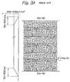
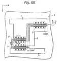
- reference numeral 1designates a glass substrate on which a substrate covering layer 2 made of silicon oxide is formed. Also, a polycrystalline silicon island 3 ′ including a source region S, a channel region C and a drain region D is formed on the substrate covering layer 2 . The polycrystalline silicon island 3 ′ is covered by gate insulating layers 4 - 1 and 4 - 2 . Note that the gate insulating layers 4 - 1 and 4 - 2 can be formed by a single layer.
- patterned gate electrode layers 5 - 1 and 5 - 2are formed on the gate insulating layers 4 - 1 and 4 - 2 .
- the patterned gate electrode layers 5 - 1 and 5 - 2are covered by a passivation layer 6 . Note that the patterned gate electrode layers 5 - 1 and 5 - 2 can be formed by a single layer.
- contact holesare perforated in the gate insulating layers 4 - 1 and 4 - 2 and the passivation layer 6 .
- a metal layer 7is buried in the contact holes.
- the polycrystalline silicon island 3 ′ of FIG. 1is formed by using a pulse layer irradiation apparatus as illustrated in FIG. 2.
- laser beams emitted from a pulse laser source 201passes through mirrors 202 and 203 , a beam homogenizer 204 and a mirror 205 to reach a target 206 .
- the target 206is formed by a glass substrate 2061 , a substrate covering layer 2062 and an amorphous silicon layer 2063 .
- a substrate covering layer 2 made of silicon oxideis deposited on a glass substrate 1 by a low pressure chemical vapor deposition (LPCVD) process or the like.
- LPCVDlow pressure chemical vapor deposition
- an amorphous silicon (a-Si) layeris deposited on the substrate covering layer 2 by an LPCVD process or the like.
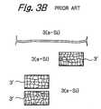
- the amorphous silicon layeris irradiated with a laser beam emitted from the pulse laser apparatus of FIG. 2 by moving the glass substrate 1 along X- and Y-directions.
- the laser beamhas a square size of several millimeters or several hundred micrometers.
- the energy of the laser beamis relatively low, for example, about 300 to 500 mJ/cm 2 , and also, the slope of the energy with respect to the X- or Y-direction is relatively gentle.
- the amorphous silicon layeris converted into a polycrystalline silicon layer which has a randomly-small grain size as shown in FIG. 3A.
- polycrystalline silicon islands 3 ′are formed by performing a photolithography and etching process upon the polycrystalline silicon layer.
- gate insulating layers 4 - 1 and 4 - 2patterned gate electrode layers 5 - 1 and 5 - 2 , a passivation layer 6 , and a metal layer 7 are formed to complete the TFT of FIG. 1.
- FIGS. 4A, 4B, 5 A, 5 B, 6 A, 6 B, 7 A, 7 B, 8 A and 8 Bare cross-sectional views taken along the line A-A of FIGS. 4B, 5B, 6 B, 7 B and 8 B, respectively.
- an about 0.5 to 1.1 mm thick glass substrate 1is subject to a cleaning and rinsing process to remove contaminants such as organic matter, metal or small particles from the surface of the glass substrate 1 .
- an about 1 ⁇ m thick substrate covering layer 2 made of silicon oxideis deposited on the glass substrate 1 by an LPCVD process using silane gas and oxygen gas.
- the substrate covering layer 2can be deposited by a plasma CVD process using tetraethoxysilane (TEOS) gas and oxygen gas an atmospheric pressure CVD (APCVD) process using TEOS gas and ozone gas, or a remote plasma CVD process where a deposition area is separated from a plasma gas generation area. Then, an about 60 to 80 nm thick amorphous silicon layer 3 is deposited on the substrate covering layer 2 by an LPCVD process using disilane gas at a temperature of about 500° C. In this case, the hydrogen concentration of the amorphous silicon layer 3 is less than 1 atom percent to prevent the emission of hydrogen atoms from the amorphous silicon layer 3 by a laser irradiation process which will be carried out later.
- TEOStetraethoxysilane
- APCVDatmospheric pressure CVD
- the surface of a polycrystalline silicon layer converted therefromgreatly fluctuates.
- the above-mentioned amorphous silicon layer 3 having a low hydrogen concentrationcan be deposited by a plasma CVD process using silane gas and hydrogen gas, or tetrafluoro-silane gas and hydrogen gas.
- the glass substrate 1is again subject to a cleaning and rinsing process to remove contaminants such as organic matter, metal, small particles and silicon oxide from the surface of the amorphous silicon layer 3 .
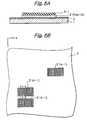
- the glass substrate 1is entered into the pulse laser apparatus of FIG. 2 where the amorphous silicon layer 3 is irradiated with laser line beams under an atmosphere of pure nitrogen gas at a 700 Torr (8.33 ⁇ 10 4 Pa).
- the laser line beamshave a rectangular size of 5 ⁇ m ⁇ 100 ⁇ m.
- the energy of the laser beamsis relatively high, for example, about 400 to 900 mJ/am 2 , and also, the slope of the energy with respect to the Y-direction is relatively sharp.
- the growth of polycrystalline silicon stops at YY 3 and Y 3 ′.
- a polycrystalline silicon layer 3 ′is obtained to include elongated grains having a length of an approximately half of the width of the laser line beams.
- the polycrystalline silicon layer 3 ′has stripes each of which is divided into two regions 31 and 32 . Then, nitrogen is exhausted from the pulse laser apparatus, and then, oxygen gas is introduced thereinto.
- an about 10 nm thick gate insulating layer 4 - 1 made of silicon oxideis deposited on the entire surface by a plasma CVD process using silane gas, helium gas and oxygen gas at a temperature of about 350° C.
- the gate insulating layer 4 - 1can be deposited by a plasma CVD process using TEOS gas and oxygen gas or an APCVD process using TEOS gas and ozone gas. Thereafter, as occasion demands, a hydrogen plasma process and an annealing process are carried out.
- the gate insulating layer 4 - 1 and the polycrystalline silicon layer 3 ′are patterned by a photolithography and etching process, so that islands formed by the gate insulating layer 4 - 1 and the polycrystalline silicon layer 3 ′ are formed.
- the sides of the islands ( 3 ′, 4 - 1 )are tapered to suppress gate leakage currents.
- the gate insulating layer 4 - 1can be deleted.
- the glass substrate 1is again subject to a cleaning and rinsing process to remove contaminants such as organic matter, metal and small particles from the surface of the gate insulating layer 4 - 1 and the like.
- an about 30 nm thick gate insulating layer 4 - 2 made of silicon oxideis deposited on the entire surface by a plasma CVD process using silane gas and oxygen gas at a temperature of about 450° C.
- the gate insulating layer 4 - 2can be deposited by a plasma CVD process using TEOS gas and oxygen gas or an APCVD process using TEOS gas and ozone gas.
- gate electrode layer 5 - 1made of phosphorus-doped polycrystalline silicon is deposited on the gate insulating layer 4 - 2 by a plasma CVD process or an LPCVD process, and an about 110 nm thick gate electrode layer 5 - 2 made of tungsten silicide is deposited on the gate electrode layer 5 - 1 by a sputtering process.
- the gate electrode layers 5 - 1 and 5 - 2are patterned by a photolithography and etching process.
- impurity ionsare implanted into the polycrystalline silicon islands 3 ′ in self-alignment with the patterned gate electrode layers 5 - 1 and 5 - 2 .
- source regions S and drain regions D of an n + -typeare formed within the polycrystalline silicon islands 3 ′.
- the impurity ionsare of a p-type, source regions S and drain regions D of a p + -type are formed within the polycrystalline silicon islands 3 ′.
- undoped regions of the polycrystalline silicon islands 3 ′serve as channel regions C.
- a passivation layer 6 made of silicon oxideis deposited on the entire surface by a plasma CVD process using TEOS gas and oxygen gas or an APCVD process using TEOS gas and ozone gas.
- the passivation layer 6can be made of silica coating material or organic coating material, silicon nitride.
- the passivation layer 6is flatten by an annealing process or the like.
- contact holes CONTare perforated in the gate insulating layers 4 - 1 and 4 - 2 and the passivation layer 6 by a photolithography and etching process thereupon.
- a metal layer 7 made of aluminum, aluminum alloy, copper, copper alloy or refractory metal such as tungsten or molybdenumis deposited on the entire surface by a sputtering process or the like, and the metal layer 7 is patterned by a photolithography and etching process.
- CMOS inverterformed by a P-channel TFT and two N-channel TFTs.
- FIGS. 9 and 10which are cross-sectional views of modifications of FIGS. 7A and 8A, respectively, the implantion of impurity ions is performed directly upon the polycrystalline silicon islands 3 ′.
- the gate insulating layers 4 - 1 and 4 - 2are etched by using the gate electrode layers. 5 - 1 and 5 - 2 as an etching mask before the implantation of impurity ions.
- the irradiation of laser line beams to the amorphous silicon layer 3can be carried out by using alignment marks.
- the alignment marks made of tungsten silicide or the likeare formed on the substrate covering layer 2 before the irradiation of laser beams to the amorphous silicon layer 3 .
- alignment marksare formed on the amorphous silicon layer 3 simultaneously with the irradiation of laser line beams to the amorphous silicon layer 3 .
- the patterning of the polycrystalline silicon layer 3 ′ into the islandsis carried out by using the above-mentioned alignment marks.
- FIGS. 11A and 11Bare SEM photographs as shown in FIGS. 11A and 11B.
- FIG. 11Bis an enlargement of FIG. 11A.
- the polycrystalline silicon layer 3 ′has elongated grains along the Y direction and is divided into the two regions 31 and 32 .
- the TFTsare formed so that the running direction of carriers is along the Y direction, i.e., the growth direction of crystal, the mobility of carriers is so high that the ON current is high. Additionally, since each of the TFTs are formed within either of the regions 31 and 32 , the mobility of carriers is further increased, so that the ON current is further increased. Note that if each of the TFTs is formed across the regions 31 and 32 , the mobility of carriers is a little decreased so that the ON current is a little decreased.
- a first exampleis a digital camera as illustrated in FIGS. 12, 13, 14 and 15 .
- a digital camerais constructed by a camera body 1201 on which a lens 1202 is mounted.
- An image input unit 1203is incorporated into the camera body 1201 .
- the image input unit 1203has the same size as the size of a 35-mm photographic film. Therefore, in the digital camera of FIG. 12, the image input unit 1203 can be replaced with 35-mm photographic films.
- a microcomputer 1204formed by a central processing unit (CPU), a flash memory, an encoder, an interface and the like is incorporated into the camera body 1201 , and can be connected by a flexible cable 1205 to the image input unit 1203 .
- FIG. 13which is a detailed plan view of the image input unit 1203 of FIG. 12, the image input unit 1203 is constructed by a glass substrate 1301 corresponding to the glass substrate 1 of the embodiment of the TFT according to the present invention, a pixel array section 1302 , and peripheral circuits such as an X-scanning circuit 1303 , a Y-scanning circuit 1304 and a reset circuit 1305 .
- the glass substrate 1301is 1.1 mm, 0.7 mm or 0.5 mm thick, and has a size of 48 mm ⁇ 35 mm.
- the pixel array section 1302has a size of 36 mm ⁇ 24 mm.
- the pixel array section 1302is constructed by a plurality of photodiode-type active pixels each including a 20 ⁇ m ⁇ 20 ⁇ m photodiode PD such as a Schottky barrier diode buffered by a source follower TFT Q 1 , a selection TFT Q 2 and a reset TFT Q 3 .
- the TFT Q 1is selected by the X-scanning circuit 1303
- the TFT Q 2is selected by the Y-scanning circuit 1304 .
- the TFT Q 3is turned ON by a reset signal RST of the reset circuit 1305 , thereby resetting the voltage of the photodiodePD at V cc , (see: Eric R. Fossum, FIG.
- CMOS Image SensorElectronic Camera On A Chip ”, IEDM Digest, pp. 17-25, 1995.
- a PIN diodecan be used as the photodiode PD.
- the TFTs Q 1 , Q 2 and Q 3are those according to the embodiment of the present invention.
- a photodiode 1302 asuch as a Schottky barrier diode is provided at a periphery area of the pixels to detect whether or not a shutter (not shown) in the camera body 1201 is opened. That is, as shown in FIG. 14(A), when the shutter is opened, the photodiode 1302 a generates a detection signal D as shown in FIG. 14(B). As a result, the reset circuit 1305 receives the detection signal D and generates a reset signal RST as shown in FIG. 14(C) in response to a rising edge of the detection signal D. Therefore, the TFTs Q 3 of all the pixels are turned ON, so that the voltage of the photodiode PD are reset at V cc .
- a photodiode 1302 asuch as a Schottky barrier diode is provided at a periphery area of the pixels to detect whether or not a shutter (not shown) in the camera body 1201 is opened. That is, as shown in FIG. 14
- the scanning circuits 1303 and 1304are operated as shown in FIG. 14(D) so that image information stored in the photodiodes PD of all the pixels are transmitted to the microcomputer 1204 which performs data processing thereupon.
- a PIN diodecan be used as the photodiode 1302 a.
- FIG. 15which is a detailed cross-sectional view of the photodiode PD and the TFT Q 3 of FIG. 13, the TFT Q 3 is formed on the glass substrate 1301 in accordance with the embodiment of the present invention. That is, the TFT Q 3 is constructed by a polycrystalline silicon island 1501 , a source region S, a channel region C and a drain region D corresponding to the polycrystalline silicon island 3 ′ of FIG. 8A or 10 , a gate electrode 1502 corresponding to the gate electrode layers 5 - 1 and 5 - 2 of FIG. 8A or 10 , and an insulating layer 1503 corresponding to the gate insulating layers 4 - 1 and 4 - 2 and the passivation layer 6 of FIG. 8A or 10 .
- a contact holeis perforated in the insulating layer 1503 above the source region S of the polycrystalline silicon island 1501 .
- a Cr lower electrode layer 1504 , an intrinsic amorphous silicon layer 1505 , a P + -type amorphous silicon layer 1506 and an upper indium tin oxide (ITO) upper transparent electrode layer 1507are sequentially formed to form the photodiode PD. Note that, if the photodiode PD is replaced by a PIN diode, an n-type amorphous silicon layer is inserted between the Cr under electrode layer 1504 and the intrinsic amorphous silicon layer 1505 .
- the TFTs Q 1 and Q 2are also formed in the same way as the TFT Q 1 , so that the photodiode PD is formed over the TFTs Q 1 , Q 2 and Q 3 .
- a second exampleis an SRAM cell as illustrated in FIG. 16.
- one memory cellis provided at each intersection between two word lines WL 1 and WL 2 and two complementary date lines DL 1 and DL 2 .
- memory cellis constructed by a flip-flop formed by two cross-coupled inverters, and two N-channel transfer MOS transistors Q t1 and Q t2 connected between the flip-flop and the data lines DL 1 and DL 2 .
- the transfer. transistors Q t1 and Q t2are controlled by voltages at the word lines WL 1 and WL 2 , respectively.
- Each of the invertersincludes a P-channel load TFT Q p1 (Q p2 ) and an N-channel driving bulk MOS transistor Q d1 (Q d2 ) between a power supply voltage line V cc and a ground voltage line V ss .
- the P-channel TFTs Q p1 and Q p2are those according to the present invention.
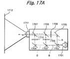
- a third exampleis a projector as illustrated in FIGS. 17A and 17B.
- the projectoris constructed by a halogen lamp 1701 , dichotic lenses 1702 to 1707 , light valves 1708 , 1709 and 1710 , a projection lens 1711 and a screen 1712 .
- a red component Ris generated by the lenses 1702 , 1705 , 1706 and 1707 and the light valve 1708 ;
- a blue component Bis generated by the lenses 1702 , 1703 , 1706 and 1707 and the light valve 1709 ;
- a green component Gis generated by the lenses 1702 , 1703 , 1704 and 1707 and the light valve 1710 .
- each of the light valves 1708 , 1709 and 1710is an active matrix-type liquid crystal display (LCD) apparatus which is constructed by a plurality of pixels P ij at intersections between data bus lines DL i and gate bus lines GL j .
- One of the data bus lines SL iis driven by a data driver 1721 and one of the gate bus lines GL j is driven by a gate driver 1722 .
- each of the pixels P ijis constructed by one TFT Q and one liquid crystal cell C.
- the TFT Qis one according to the embodiment of the present invention.
- the mobility of carrierscan be increased, and accordingly, the ON current can be increased.
Landscapes
- Thin Film Transistor (AREA)
Abstract
Description
- 1. Field of the Invention[0001]
- The present invention relates to a thin film transistor (TFT), a method for manufacturing the TFT, and apparatuses using the TFT.[0002]
- 2. Description of the Related Art[0003]
- Generally, TFTs are manufactured on an insulating substrate by using a hydrogen-passivated amorphous silicon technology and a polycrystalline silicon technology.[0004]
- According to the hydrogen-passivated amorphous silicon technology, since the maximum temperature during the manufacturing steps thereof is low, i.e., about 300° C., the mobility of carriers is low,i.e., about 1 cm[0005]2/V·sec. Also, an insulating substrate can be a glass substrate having a low melting temperature, which would decrease the manufacturing cost.
- However, in an active matrix-type liquid crystal display (LCD) apparatus manufactured by the hydrogen-passivated amorphous silicon technology, TFTs manufactured by the hydrogen-passivated amorphous silicon technology are used as the switching elements of pixels of a display panel of the LCD apparatus, and the TFTs are driven by a driver of an integrated circuit apparatus connected to a periphery of the display panel. As a result, since the display panel is connected to the driver for driving the display panel by a tape automated bonding (TAB) process or a wire bonding process, if the connection pitch between the display panel and the driver becomes small, it is actually impossible to connect the display panel to the driver.[0006]
- On the other hand, according to the polycrystalline silicon technology, since the maximum temperature during the manufacturing steps thereof is high, i.e., about 1000° C., the mobility of carriers is about 30 to 100 cm[0007]2/V·sec. For example, a high temperature annealing process is required to convert amorphous silicon into polycrystalline silicon. Also, if TFTs manufactured by the polycrystalline silicon technology are used as the switching elements of pixels of a display panel of an active matrix-type LCD apparatus, a driver for driving the display panel can also be formed on the same substrate of the display panel, so that the above-mentioned theremocompressing bonding process or wire bonding process is unnecessary.
- In the polycrystalline silicon technology, since the maximum temperature is high as stated above, the insulating substrate has to be a fused quart substrate having a high melting temperature, for example. This would increase the manufacturing cost.[0008]
- In order to decrease the manufacturing cost, i.e., in order to decrease the temperature for converting amorphous silicon into polycrystalline silicon to adopt a glass substrate having a low melting temperature, a laser technology has been combined with the polycrystalline silicon technology.[0009]
- In a prior art method for manufacturing a TFT by the polycrystalline silicon technology combined with the laser technology, first, a substrate covering layer made of silicon oxide is deposited on a glass substrate by a low pressure chemical vapor deposition (LPCVD) process or the like. Next, an amorphous silicon (a-Si) layer is deposited on the substrate covering layer by an LPCVD process or the like. Next, the amorphous silicon layer is irradiated with a laser beam by moving the glass substrate along X-and Y-directions. This will be explained later in detail.[0010]
- In the above-described prior art method, however, the laser beam has a rectangular size of several millimeters or several hundred micrometers. Additionally, the energy of the laser beam is relatively low, for example, 300 mJ/cm[0011]2, and also, the slope of the energy with respect to the X- or Y-direction is relatively gentle. As a result, the amorphous silicon layer is converted into a polycrystalline silicon layer which has a randomly-small grain size. Thus, since the polycrystalline silicon layer forming a source region, a channel region and a drain region has a randomly-small grain size, the mobility of carriers is so low that the ON-current is low.
- It is an object of the present invention to provide a TFT having a high mobility of carriers and a high ON-current and a method for manufacturing such a TFT.[0012]
- Another object is to provide various kinds of apparatuses using such a TFT.[0013]
- According to the present invention, in a TFT including an insulating substrate and a polycrystalline silicon island formed on the insulating layer, a grain size of the polycrystalline silicon island is elongated along one direction. A source region, a channel region and a drain region are arranged in the polycrystalline silicon island in parallel with the direction.[0014]
- Also, in a method for manufacturing a TFT, an amorphous silicon layer is formed oh an insulating substrate. Then, the amorphous silicon layer is irradiated with a laser line beam along one direction, so that a portion of the amorphous silicon layer irradiated with the laser line beam is converted into a polycrystalline silicon layer. Then, the polycrystalline silicon layer is patterned into a polycrystalline silicon island. Then, a source region, a channel region and a drain region of the TFT are formed in the polycrystalline silicon island.[0015]
- The present invention will be more clearly understood from the description set forth below, as compared with the prior art, with reference to the accompanying drawings, wherein:[0016]
- FIG. 1 is a cross-sectional views illustrating a prior art TFT;[0017]
- FIG. 2 is a diagram illustrating a pulse laser apparatus for manufacturing the polycrystalline silicon island of FIG. 1;[0018]
- FIGS. 3A and 3B are plan views for explaining a prior art method for manufacturing the TFT of FIG. 1;[0019]
- FIGS. 4A, 5A,[0020]6A,7A and8B are cross-sectional views for explaining an embodiment of the method for manufacturing a TFT according to the present invention;
- FIGS. 4B, 5B,[0021]6B,7B and8B are plan views of the TFT of FIGS. 4A, 5A,6A,7A and BA, respectively;
- FIGS. 9 and 10 are cross-sectional view illustrating modifications of FIGS. 7A and 8A, respectively;[0022]
- FIGS. 11A and 11B are scanning electron microscope (SEM) photographs showing the polycrystalline silicon layer of FIGS. 5A and 5B;[0023]
- FIG. 12 is a diagram illustrating a digital camera to which the TFT according to the present invention is applied;[0024]
- FIG. 13 is a detailed plan view of the image input unit of FIG. 12;[0025]
- FIG. 14 is a timing diagram for showing the operation of the image input unit of FIG. 13;[0026]
- FIG. 15 is a cross-sectional view of the photodiode and the reset TFT of FIG. 13;[0027]
- FIG. 16 is a circuit diagram illustrating a static random access memory (SRAM) cell to which the TFT according to the present invention is applied; and[0028]
- FIG. 17A is a diagram illustrating a projector to which the TFT according to the present invention is applied; and[0029]
- FIG. 17B is a circuit diagram of the light valve of FIG. 17A.[0030]
- Before the description of the preferred embodiment, a prior art method for manufacturing a TFT will be explained with reference to FIGS. 1, 2,[0031]3A and3B.
- In FIG. 1, which illustrates a prior art TFT,[0032]
reference numeral 1 designates a glass substrate on which a substrate coveringlayer 2 made of silicon oxide is formed. Also, apolycrystalline silicon island 3′ including a source region S, a channel region C and a drain region D is formed on thesubstrate covering layer 2. Thepolycrystalline silicon island 3′ is covered by gate insulating layers4-1 and4-2. Note that the gate insulating layers4-1 and4-2 can be formed by a single layer. - Additionally, patterned gate electrode layers[0033]5-1 and5-2 are formed on the gate insulating layers4-1 and4-2. The patterned gate electrode layers5-1 and5-2 are covered by a
passivation layer 6. Note that the patterned gate electrode layers5-1 and5-2 can be formed by a single layer. - Further, contact holes are perforated in the gate insulating layers[0034]4-1 and4-2 and the
passivation layer 6. Ametal layer 7 is buried in the contact holes. - The[0035]
polycrystalline silicon island 3′ of FIG. 1 is formed by using a pulse layer irradiation apparatus as illustrated in FIG. 2. - In FIG. 2, laser beams emitted from a[0036]
pulse laser source 201 passes throughmirrors beam homogenizer 204 and amirror 205 to reach atarget 206. For example, thetarget 206 is formed by aglass substrate 2061, asubstrate covering layer 2062 and anamorphous silicon layer 2063. - A prior art method for manufacturing the TFT of FIG. 1 will be explained next with reference to FIGS. 3A and 3B.[0037]
- First, a[0038]
substrate covering layer 2 made of silicon oxide is deposited on aglass substrate 1 by a low pressure chemical vapor deposition (LPCVD) process or the like. - Next, an amorphous silicon (a-Si) layer is deposited on the[0039]
substrate covering layer 2 by an LPCVD process or the like. - Next, referring to FIG. 3A, the amorphous silicon layer is irradiated with a laser beam emitted from the pulse laser apparatus of FIG. 2 by moving the[0040]
glass substrate 1 along X- and Y-directions. In this case, the laser beam has a square size of several millimeters or several hundred micrometers. Additionally, the energy of the laser beam is relatively low, for example, about 300 to 500 mJ/cm2, and also, the slope of the energy with respect to the X- or Y-direction is relatively gentle. As a result, the amorphous silicon layer is converted into a polycrystalline silicon layer which has a randomly-small grain size as shown in FIG. 3A. - Next, referring to FIG. 3B,[0041]
polycrystalline silicon islands 3′ are formed by performing a photolithography and etching process upon the polycrystalline silicon layer. - Thereafter, gate insulating layers[0042]4-1 and4-2, patterned gate electrode layers5-1 and5-2, a
passivation layer 6, and ametal layer 7 are formed to complete the TFT of FIG. 1. - In the manufacturing method as shown in FIGS. 3A and 3B, however, since the[0043]
polycrystalline silicon island 3 has a randomly-small grain size, the mobility of carriers is so low that the ON-current is low. - An embodiment of the method for manufacturing a TFT according to the present invention will be explained next with reference to FIGS. 4A, 4B,[0044]5A,5B,6A,6B,7A,7B,8A and8B. Note that FIGS. 4A, 5A,6A,7A and8A are cross-sectional views taken along the line A-A of FIGS. 4B, 5B,6B,7B and8B, respectively.
- First, referring to FIGS. 4A and 4B, an about 0.5 to 1.1 mm[0045]
thick glass substrate 1 is subject to a cleaning and rinsing process to remove contaminants such as organic matter, metal or small particles from the surface of theglass substrate 1. Then, in order to prevent harmful impurities from diffusing from theglass substrate 1, an about 1 μm thicksubstrate covering layer 2 made of silicon oxide is deposited on theglass substrate 1 by an LPCVD process using silane gas and oxygen gas. Note that thesubstrate covering layer 2 can be deposited by a plasma CVD process using tetraethoxysilane (TEOS) gas and oxygen gas an atmospheric pressure CVD (APCVD) process using TEOS gas and ozone gas, or a remote plasma CVD process where a deposition area is separated from a plasma gas generation area. Then, an about 60 to 80 nm thickamorphous silicon layer 3 is deposited on thesubstrate covering layer 2 by an LPCVD process using disilane gas at a temperature of about 500° C. In this case, the hydrogen concentration of theamorphous silicon layer 3 is less than 1 atom percent to prevent the emission of hydrogen atoms from theamorphous silicon layer 3 by a laser irradiation process which will be carried out later. If a large number of hydrogen atoms are emitted from theamorphous silicon layer 3, the surface of a polycrystalline silicon layer converted therefrom greatly fluctuates. Also, the above-mentionedamorphous silicon layer 3 having a low hydrogen concentration can be deposited by a plasma CVD process using silane gas and hydrogen gas, or tetrafluoro-silane gas and hydrogen gas. - Next, referring to FIGS. 5A and 5B, the[0046]
glass substrate 1 is again subject to a cleaning and rinsing process to remove contaminants such as organic matter, metal, small particles and silicon oxide from the surface of theamorphous silicon layer 3. Then, theglass substrate 1 is entered into the pulse laser apparatus of FIG. 2 where theamorphous silicon layer 3 is irradiated with laser line beams under an atmosphere of pure nitrogen gas at a 700 Torr (8.33×10⁴Pa). In this case, the laser line beams have a rectangular size of 5 μm×100 μm. Also, the energy of the laser beams is relatively high, for example, about 400 to 900 mJ/am2, and also, the slope of the energy with respect to the Y-direction is relatively sharp. As a result, as illustrated in FIG. 5B, crystalline silicon seeds (not shown) are randomly generated at portions of theamorphous silicon layer 3 at Y=Y1, Y2, Y1′ and Y2′ where the temperature is close to a melting point of silicon. Then, polycrystalline silicon is grown from the crystalline silicon seeds toward the center of each of the laser line beams at Y=Y3 and Y3′. Finally, the growth of polycrystalline silicon stops at Y=Y3 and Y3′. Thus, apolycrystalline silicon layer 3′ is obtained to include elongated grains having a length of an approximately half of the width of the laser line beams. As a result, thepolycrystalline silicon layer 3′ has stripes each of which is divided into tworegions - Next, referring to FIGS. 6A and 6B, an about 10 nm thick gate insulating layer[0047]4-1 made of silicon oxide is deposited on the entire surface by a plasma CVD process using silane gas, helium gas and oxygen gas at a temperature of about 350° C. Note that the gate insulating layer4-1 can be deposited by a plasma CVD process using TEOS gas and oxygen gas or an APCVD process using TEOS gas and ozone gas. Thereafter, as occasion demands, a hydrogen plasma process and an annealing process are carried out. Then, the gate insulating layer4-1 and the
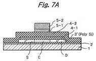
polycrystalline silicon layer 3′ are patterned by a photolithography and etching process, so that islands formed by the gate insulating layer4-1 and thepolycrystalline silicon layer 3′ are formed. In this case, the sides of the islands (3′,4-1) are tapered to suppress gate leakage currents. However, the gate insulating layer4-1 can be deleted. - Next, referring to FIGS. 7A and 7B, the[0048]
glass substrate 1 is again subject to a cleaning and rinsing process to remove contaminants such as organic matter, metal and small particles from the surface of the gate insulating layer4-1 and the like. Then, an about 30 nm thick gate insulating layer4-2 made of silicon oxide is deposited on the entire surface by a plasma CVD process using silane gas and oxygen gas at a temperature of about 450° C. Note that the gate insulating layer4-2 can be deposited by a plasma CVD process using TEOS gas and oxygen gas or an APCVD process using TEOS gas and ozone gas. Then, an about 80 nm thick gate electrode layer5-1 made of phosphorus-doped polycrystalline silicon is deposited on the gate insulating layer4-2 by a plasma CVD process or an LPCVD process, and an about 110 nm thick gate electrode layer5-2 made of tungsten silicide is deposited on the gate electrode layer5-1 by a sputtering process. Then, the gate electrode layers5-1 and5-2 are patterned by a photolithography and etching process. Then, impurity ions are implanted into thepolycrystalline silicon islands 3′ in self-alignment with the patterned gate electrode layers5-1 and5-2. For example, if the impurity ions are of an n-type, source regions S and drain regions D of an n+-type are formed within thepolycrystalline silicon islands 3′. On the other hand, if the impurity ions are of a p-type, source regions S and drain regions D of a p+-type are formed within thepolycrystalline silicon islands 3′. Note that undoped regions of thepolycrystalline silicon islands 3′ serve as channel regions C. - Finally, referring to FIGS. 8A and 8B, a[0049]
passivation layer 6 made of silicon oxide is deposited on the entire surface by a plasma CVD process using TEOS gas and oxygen gas or an APCVD process using TEOS gas and ozone gas. Note that, thepassivation layer 6 can be made of silica coating material or organic coating material, silicon nitride. As occasion demands, thepassivation layer 6 is flatten by an annealing process or the like. Then, contact holes CONT are perforated in the gate insulating layers4-1 and4-2 and thepassivation layer 6 by a photolithography and etching process thereupon. Then, ametal layer 7 made of aluminum, aluminum alloy, copper, copper alloy or refractory metal such as tungsten or molybdenum is deposited on the entire surface by a sputtering process or the like, and themetal layer 7 is patterned by a photolithography and etching process. - In FIG. 8B, note that a CMOS inverter formed by a P-channel TFT and two N-channel TFTs.[0050]
- In FIGS. 9 and 10, which are cross-sectional views of modifications of FIGS. 7A and 8A, respectively, the implantion of impurity ions is performed directly upon the[0051]
polycrystalline silicon islands 3′. In this case, the gate insulating layers4-1 and4-2 are etched by using the gate electrode layers.5-1 and5-2 as an etching mask before the implantation of impurity ions. - In the above-described embodiment, the irradiation of laser line beams to the[0052]
amorphous silicon layer 3 can be carried out by using alignment marks. For example, the alignment marks made of tungsten silicide or the like are formed on thesubstrate covering layer 2 before the irradiation of laser beams to theamorphous silicon layer 3. On the other hand, alignment marks are formed on theamorphous silicon layer 3 simultaneously with the irradiation of laser line beams to theamorphous silicon layer 3. Thereafter, the patterning of thepolycrystalline silicon layer 3′ into the islands is carried out by using the above-mentioned alignment marks. - The inventors have actually obtained the[0053]
polycrystalline silicon layer 3′ of FIGS. 5A and 5B as shown in SEM photographs as shown in FIGS. 11A and 11B. Note that FIG. 11B is an enlargement of FIG. 11A. Apparently, thepolycrystalline silicon layer 3′ has elongated grains along the Y direction and is divided into the tworegions - In the above-described embodiments, since the TFTs are formed so that the running direction of carriers is along the Y direction, i.e., the growth direction of crystal, the mobility of carriers is so high that the ON current is high. Additionally, since each of the TFTs are formed within either of the[0054]
regions regions - Apparatuses to which the TFT of the present invention is applied will be explained next with reference to FIGS. 12, 13,[0055]14,15,16,17A and17B.
- A first example is a digital camera as illustrated in FIGS. 12, 13,[0056]14 and15.
- In FIG. 12, a digital camera is constructed by a[0057]
camera body 1201 on which alens 1202 is mounted. Animage input unit 1203 is incorporated into thecamera body 1201. For example, theimage input unit 1203 has the same size as the size of a 35-mm photographic film. Therefore, in the digital camera of FIG. 12, theimage input unit 1203 can be replaced with 35-mm photographic films. Also, amicrocomputer 1204 formed by a central processing unit (CPU), a flash memory, an encoder, an interface and the like is incorporated into thecamera body 1201, and can be connected by aflexible cable 1205 to theimage input unit 1203. - In FIG. 13, which is a detailed plan view of the[0058]
image input unit 1203 of FIG. 12, theimage input unit 1203 is constructed by aglass substrate 1301 corresponding to theglass substrate 1 of the embodiment of the TFT according to the present invention, apixel array section 1302, and peripheral circuits such as anX-scanning circuit 1303, a Y-scanning circuit 1304 and areset circuit 1305. In this case, theglass substrate 1301 is 1.1 mm, 0.7 mm or 0.5 mm thick, and has a size of 48 mm×35 mm. Also, thepixel array section 1302 has a size of 36 mm×24 mm. - The[0059]
pixel array section 1302 is constructed by a plurality of photodiode-type active pixels each including a 20 μm×20 μm photodiode PD such as a Schottky barrier diode buffered by a source follower TFT Q1, a selection TFT Q2 and a reset TFT Q3. The TFT Q1 is selected by theX-scanning circuit 1303, while the TFT Q2 is selected by the Y-scanning circuit 1304. Also, the TFT Q3 is turned ON by a reset signal RST of thereset circuit 1305, thereby resetting the voltage of the photodiodePD at Vcc, (see: Eric R. Fossum, FIG. 4 of “CMOS Image Sensor: Electronic Camera On A Chip ”, IEDM Digest, pp. 17-25, 1995). Note that a PIN diode can be used as the photodiode PD. The TFTs Q1, Q2 and Q3 are those according to the embodiment of the present invention. - Also, a[0060]
photodiode 1302asuch as a Schottky barrier diode is provided at a periphery area of the pixels to detect whether or not a shutter (not shown) in thecamera body 1201 is opened. That is, as shown in FIG. 14(A), when the shutter is opened, thephotodiode 1302agenerates a detection signal D as shown in FIG. 14(B). As a result, thereset circuit 1305 receives the detection signal D and generates a reset signal RST as shown in FIG. 14(C) in response to a rising edge of the detection signal D. Therefore, the TFTs Q3 of all the pixels are turned ON, so that the voltage of the photodiode PD are reset at Vcc. Then, when a predetermined time period has passed after the reset signal RST is generated, thescanning circuits microcomputer 1204 which performs data processing thereupon. Note that a PIN diode can be used as thephotodiode 1302a. - In FIG. 15, which is a detailed cross-sectional view of the photodiode PD and the TFT Q[0061]3 of FIG. 13, the TFT Q3 is formed on the
glass substrate 1301 in accordance with the embodiment of the present invention. That is, the TFT Q3 is constructed by apolycrystalline silicon island 1501, a source region S, a channel region C and a drain region D corresponding to thepolycrystalline silicon island 3′ of FIG. 8A or10, agate electrode 1502 corresponding to the gate electrode layers5-1 and5-2 of FIG. 8A or10, and an insulatinglayer 1503 corresponding to the gate insulating layers4-1 and4-2 and thepassivation layer 6 of FIG. 8A or10. Also, a contact hole is perforated in the insulatinglayer 1503 above the source region S of thepolycrystalline silicon island 1501. Further, a Crlower electrode layer 1504, an intrinsicamorphous silicon layer 1505, a P+-typeamorphous silicon layer 1506 and an upper indium tin oxide (ITO) uppertransparent electrode layer 1507 are sequentially formed to form the photodiode PD. Note that, if the photodiode PD is replaced by a PIN diode, an n-type amorphous silicon layer is inserted between the Cr underelectrode layer 1504 and the intrinsicamorphous silicon layer 1505. - In FIG. 15, only the TFT Q[0062]3 is illustrated, however, the TFTs Q1 and Q2 are also formed in the same way as the TFT Q1, so that the photodiode PD is formed over the TFTs Q1, Q2 and Q3.
- A second example is an SRAM cell as illustrated in FIG. 16. In FIG. 16, one memory cell is provided at each intersection between two word lines WL[0063]1 and WL2 and two complementary date lines DL1 and DL2. Thus memory cell is constructed by a flip-flop formed by two cross-coupled inverters, and two N-channel transfer MOS transistors Qt1and Qt2connected between the flip-flop and the data lines DL1 and DL2. The transfer. transistors Qt1and Qt2are controlled by voltages at the word lines WL1 and WL2, respectively. Each of the inverters includes a P-channel load TFT Qp1(Qp2) and an N-channel driving bulk MOS transistor Qd1(Qd2) between a power supply voltage line Vccand a ground voltage line Vss.
- The P-channel TFTs Q[0064]p1and Qp2are those according to the present invention.
- A third example is a projector as illustrated in FIGS. 17A and 17B.[0065]
- In FIG. 17A, the projector is constructed by a[0066]
halogen lamp 1701,dichotic lenses 1702 to1707,light valves projection lens 1711 and ascreen 1712. In this case, a red component R is generated by thelenses light valve 1708; a blue component B is generated by thelenses light valve 1709; and a green component G is generated by thelenses light valve 1710. - As illustrated in FIG. 17B, each of the[0067]
light valves data driver 1721 and one of the gate bus lines GLjis driven by agate driver 1722. Also, each of the pixels Pijis constructed by one TFT Q and one liquid crystal cell C. The TFT Q is one according to the embodiment of the present invention. - As explained hereinabove according to the present invention, in a TFT, the mobility of carriers can be increased, and accordingly, the ON current can be increased.[0068]
Claims (24)
Priority Applications (2)
| Application Number | Priority Date | Filing Date | Title |
|---|---|---|---|
| US10/815,393US7138303B2 (en) | 2000-11-20 | 2004-04-01 | Method for manufacturing a thin film transistor having high mobility and high on-current |
| US11/410,184US7285809B2 (en) | 2000-11-20 | 2006-04-24 | Thin film transistor having high mobility and high on-current |
Applications Claiming Priority (4)
| Application Number | Priority Date | Filing Date | Title |
|---|---|---|---|
| JP2000-353031 | 2000-11-20 | ||
| JP2000353031 | 2000-11-20 | ||
| US09/988,962US20020060322A1 (en) | 2000-11-20 | 2001-11-19 | Thin film transistor having high mobility and high on-current and method for manufacturing the same |
| US10/815,393US7138303B2 (en) | 2000-11-20 | 2004-04-01 | Method for manufacturing a thin film transistor having high mobility and high on-current |
Related Parent Applications (1)
| Application Number | Title | Priority Date | Filing Date |
|---|---|---|---|
| US09/988,962DivisionUS20020060322A1 (en) | 2000-11-20 | 2001-11-19 | Thin film transistor having high mobility and high on-current and method for manufacturing the same |
Related Child Applications (1)
| Application Number | Title | Priority Date | Filing Date |
|---|---|---|---|
| US11/410,184DivisionUS7285809B2 (en) | 2000-11-20 | 2006-04-24 | Thin film transistor having high mobility and high on-current |
Publications (2)
| Publication Number | Publication Date |
|---|---|
| US20040185641A1true US20040185641A1 (en) | 2004-09-23 |
| US7138303B2 US7138303B2 (en) | 2006-11-21 |
Family
ID=18825852
Family Applications (3)
| Application Number | Title | Priority Date | Filing Date |
|---|---|---|---|
| US09/988,962AbandonedUS20020060322A1 (en) | 2000-11-20 | 2001-11-19 | Thin film transistor having high mobility and high on-current and method for manufacturing the same |
| US10/815,393Expired - Fee RelatedUS7138303B2 (en) | 2000-11-20 | 2004-04-01 | Method for manufacturing a thin film transistor having high mobility and high on-current |
| US11/410,184Expired - Fee RelatedUS7285809B2 (en) | 2000-11-20 | 2006-04-24 | Thin film transistor having high mobility and high on-current |
Family Applications Before (1)
| Application Number | Title | Priority Date | Filing Date |
|---|---|---|---|
| US09/988,962AbandonedUS20020060322A1 (en) | 2000-11-20 | 2001-11-19 | Thin film transistor having high mobility and high on-current and method for manufacturing the same |
Family Applications After (1)
| Application Number | Title | Priority Date | Filing Date |
|---|---|---|---|
| US11/410,184Expired - Fee RelatedUS7285809B2 (en) | 2000-11-20 | 2006-04-24 | Thin film transistor having high mobility and high on-current |
Country Status (1)
| Country | Link |
|---|---|
| US (3) | US20020060322A1 (en) |
Cited By (41)
| Publication number | Priority date | Publication date | Assignee | Title |
|---|---|---|---|---|
| US20070164284A1 (en)* | 2005-12-29 | 2007-07-19 | Lg Philips Lcd Co., Ltd | Thin film transistor array substrate and method for manufacturing the same |
| US20070277734A1 (en)* | 2006-05-30 | 2007-12-06 | Applied Materials, Inc. | Process chamber for dielectric gapfill |
| US20080026597A1 (en)* | 2006-05-30 | 2008-01-31 | Applied Materials, Inc. | Method for depositing and curing low-k films for gapfill and conformal film applications |
| US20090061647A1 (en)* | 2007-08-27 | 2009-03-05 | Applied Materials, Inc. | Curing methods for silicon dioxide thin films deposited from alkoxysilane precursor with harp ii process |
| US20090104790A1 (en)* | 2007-10-22 | 2009-04-23 | Applied Materials, Inc. | Methods for Forming a Dielectric Layer Within Trenches |
| US20090104791A1 (en)* | 2007-10-22 | 2009-04-23 | Applied Materials, Inc. A Delaware Corporation | Methods for Forming a Silicon Oxide Layer Over a Substrate |
| US20090104789A1 (en)* | 2007-10-22 | 2009-04-23 | Applied Materials, Inc. | Method and system for improving dielectric film quality for void free gap fill |
| US7825038B2 (en) | 2006-05-30 | 2010-11-02 | Applied Materials, Inc. | Chemical vapor deposition of high quality flow-like silicon dioxide using a silicon containing precursor and atomic oxygen |
| US7867923B2 (en) | 2007-10-22 | 2011-01-11 | Applied Materials, Inc. | High quality silicon oxide films by remote plasma CVD from disilane precursors |
| US7902080B2 (en) | 2006-05-30 | 2011-03-08 | Applied Materials, Inc. | Deposition-plasma cure cycle process to enhance film quality of silicon dioxide |
| US7935643B2 (en) | 2009-08-06 | 2011-05-03 | Applied Materials, Inc. | Stress management for tensile films |
| US7989365B2 (en) | 2009-08-18 | 2011-08-02 | Applied Materials, Inc. | Remote plasma source seasoning |
| US7994019B1 (en) | 2010-04-01 | 2011-08-09 | Applied Materials, Inc. | Silicon-ozone CVD with reduced pattern loading using incubation period deposition |
| US8232176B2 (en) | 2006-06-22 | 2012-07-31 | Applied Materials, Inc. | Dielectric deposition and etch back processes for bottom up gapfill |
| US8236708B2 (en) | 2010-03-09 | 2012-08-07 | Applied Materials, Inc. | Reduced pattern loading using bis(diethylamino)silane (C8H22N2Si) as silicon precursor |
| US8304351B2 (en) | 2010-01-07 | 2012-11-06 | Applied Materials, Inc. | In-situ ozone cure for radical-component CVD |
| US8318584B2 (en) | 2010-07-30 | 2012-11-27 | Applied Materials, Inc. | Oxide-rich liner layer for flowable CVD gapfill |
| US8329262B2 (en) | 2010-01-05 | 2012-12-11 | Applied Materials, Inc. | Dielectric film formation using inert gas excitation |
| US8357435B2 (en) | 2008-05-09 | 2013-01-22 | Applied Materials, Inc. | Flowable dielectric equipment and processes |
| US8445078B2 (en) | 2011-04-20 | 2013-05-21 | Applied Materials, Inc. | Low temperature silicon oxide conversion |
| US8449942B2 (en) | 2009-11-12 | 2013-05-28 | Applied Materials, Inc. | Methods of curing non-carbon flowable CVD films |
| US8450191B2 (en) | 2011-01-24 | 2013-05-28 | Applied Materials, Inc. | Polysilicon films by HDP-CVD |
| US8466073B2 (en) | 2011-06-03 | 2013-06-18 | Applied Materials, Inc. | Capping layer for reduced outgassing |
| US8476142B2 (en) | 2010-04-12 | 2013-07-02 | Applied Materials, Inc. | Preferential dielectric gapfill |
| US8524004B2 (en) | 2010-06-16 | 2013-09-03 | Applied Materials, Inc. | Loadlock batch ozone cure |
| US8551891B2 (en) | 2011-10-04 | 2013-10-08 | Applied Materials, Inc. | Remote plasma burn-in |
| US8563445B2 (en) | 2010-03-05 | 2013-10-22 | Applied Materials, Inc. | Conformal layers by radical-component CVD |
| US8617989B2 (en) | 2011-09-26 | 2013-12-31 | Applied Materials, Inc. | Liner property improvement |
| US8629067B2 (en) | 2009-12-30 | 2014-01-14 | Applied Materials, Inc. | Dielectric film growth with radicals produced using flexible nitrogen/hydrogen ratio |
| US8647992B2 (en) | 2010-01-06 | 2014-02-11 | Applied Materials, Inc. | Flowable dielectric using oxide liner |
| US8664127B2 (en) | 2010-10-15 | 2014-03-04 | Applied Materials, Inc. | Two silicon-containing precursors for gapfill enhancing dielectric liner |
| US8716154B2 (en) | 2011-03-04 | 2014-05-06 | Applied Materials, Inc. | Reduced pattern loading using silicon oxide multi-layers |
| US8741788B2 (en) | 2009-08-06 | 2014-06-03 | Applied Materials, Inc. | Formation of silicon oxide using non-carbon flowable CVD processes |
| US8889566B2 (en) | 2012-09-11 | 2014-11-18 | Applied Materials, Inc. | Low cost flowable dielectric films |
| US8980382B2 (en) | 2009-12-02 | 2015-03-17 | Applied Materials, Inc. | Oxygen-doping for non-carbon radical-component CVD films |
| US9018108B2 (en) | 2013-01-25 | 2015-04-28 | Applied Materials, Inc. | Low shrinkage dielectric films |
| US9285168B2 (en) | 2010-10-05 | 2016-03-15 | Applied Materials, Inc. | Module for ozone cure and post-cure moisture treatment |
| US9404178B2 (en) | 2011-07-15 | 2016-08-02 | Applied Materials, Inc. | Surface treatment and deposition for reduced outgassing |
| US9412581B2 (en) | 2014-07-16 | 2016-08-09 | Applied Materials, Inc. | Low-K dielectric gapfill by flowable deposition |
| US10283321B2 (en) | 2011-01-18 | 2019-05-07 | Applied Materials, Inc. | Semiconductor processing system and methods using capacitively coupled plasma |
| US12009228B2 (en) | 2015-02-03 | 2024-06-11 | Applied Materials, Inc. | Low temperature chuck for plasma processing systems |
Families Citing this family (25)
| Publication number | Priority date | Publication date | Assignee | Title |
|---|---|---|---|---|
| US7057256B2 (en) | 2001-05-25 | 2006-06-06 | President & Fellows Of Harvard College | Silicon-based visible and near-infrared optoelectric devices |
| US7442629B2 (en) | 2004-09-24 | 2008-10-28 | President & Fellows Of Harvard College | Femtosecond laser-induced formation of submicrometer spikes on a semiconductor substrate |
| US6933527B2 (en)* | 2001-12-28 | 2005-08-23 | Semiconductor Energy Laboratory Co., Ltd. | Semiconductor device and semiconductor device production system |
| DE10340731A1 (en)* | 2003-09-04 | 2005-03-31 | Zf Friedrichshafen Ag | Multi-speed transmission |
| DE10340734A1 (en)* | 2003-09-04 | 2005-03-31 | Zf Friedrichshafen Ag | Multi-speed transmission |
| KR100573225B1 (en)* | 2003-09-24 | 2006-04-24 | 엘지.필립스 엘시디 주식회사 | Crystallization Method of Amorphous Silicon Layer |
| JP2007305698A (en)* | 2006-05-09 | 2007-11-22 | Nec Corp | Semiconductor device and manufacturing method thereof |
| JP2008177419A (en)* | 2007-01-19 | 2008-07-31 | Nissin Electric Co Ltd | Silicon thin film formation method |
| US20090219403A1 (en)* | 2008-02-29 | 2009-09-03 | Sionyx, Inc. | Compact passive low-light imaging apparatus |
| EP2629590A1 (en)* | 2008-06-17 | 2013-08-21 | Hitachi Ltd. | An organic light-emitting device |
| US20090325391A1 (en)* | 2008-06-30 | 2009-12-31 | Asm International Nv | Ozone and teos process for silicon oxide deposition |
| US9673243B2 (en) | 2009-09-17 | 2017-06-06 | Sionyx, Llc | Photosensitive imaging devices and associated methods |
| US9911781B2 (en) | 2009-09-17 | 2018-03-06 | Sionyx, Llc | Photosensitive imaging devices and associated methods |
| US8692198B2 (en) | 2010-04-21 | 2014-04-08 | Sionyx, Inc. | Photosensitive imaging devices and associated methods |
| WO2011160130A2 (en) | 2010-06-18 | 2011-12-22 | Sionyx, Inc | High speed photosensitive devices and associated methods |
| US9496308B2 (en) | 2011-06-09 | 2016-11-15 | Sionyx, Llc | Process module for increasing the response of backside illuminated photosensitive imagers and associated methods |
| WO2013010127A2 (en) | 2011-07-13 | 2013-01-17 | Sionyx, Inc. | Biometric imaging devices and associated methods |
| KR101903445B1 (en)* | 2012-01-10 | 2018-10-05 | 삼성디스플레이 주식회사 | Semiconductor device and method for manufacturing thereof |
| US9064764B2 (en) | 2012-03-22 | 2015-06-23 | Sionyx, Inc. | Pixel isolation elements, devices, and associated methods |
| US9762830B2 (en) | 2013-02-15 | 2017-09-12 | Sionyx, Llc | High dynamic range CMOS image sensor having anti-blooming properties and associated methods |
| WO2014151093A1 (en) | 2013-03-15 | 2014-09-25 | Sionyx, Inc. | Three dimensional imaging utilizing stacked imager devices and associated methods |
| US9209345B2 (en) | 2013-06-29 | 2015-12-08 | Sionyx, Inc. | Shallow trench textured regions and associated methods |
| US10141357B2 (en) | 2015-04-10 | 2018-11-27 | Sharp Kabushiki Kaisha | Photosensor substrate |
| US10756132B2 (en) | 2016-03-29 | 2020-08-25 | Sony Corporation | Solid-state imaging device, method of manufacturing the same, and electronic apparatus |
| CN106783869B (en)* | 2016-09-07 | 2019-11-22 | 武汉华星光电技术有限公司 | Thin film transistor array substrate and manufacturing method thereof |
Citations (7)
| Publication number | Priority date | Publication date | Assignee | Title |
|---|---|---|---|---|
| US4528480A (en)* | 1981-12-28 | 1985-07-09 | Nippon Telegraph & Telephone | AC Drive type electroluminescent display device |
| US5776803A (en)* | 1995-10-25 | 1998-07-07 | U.S. Philips Corporation | Manufacture of electronic devices comprising thin-film circuitry on a polymer substrate |
| US6025217A (en)* | 1994-11-24 | 2000-02-15 | Sony Corporation | Method of forming polycrystalline semiconductor thin film |
| US6177301B1 (en)* | 1998-06-09 | 2001-01-23 | Lg.Philips Lcd Co., Ltd. | Method of fabricating thin film transistors for a liquid crystal display |
| US6184541B1 (en)* | 1997-12-04 | 2001-02-06 | Matsushita Electronics Corporation | Thin film transistor and method of producing the same |
| US6479837B1 (en)* | 1998-07-06 | 2002-11-12 | Matsushita Electric Industrial Co., Ltd. | Thin film transistor and liquid crystal display unit |
| US6504175B1 (en)* | 1998-04-28 | 2003-01-07 | Xerox Corporation | Hybrid polycrystalline and amorphous silicon structures on a shared substrate |
Family Cites Families (8)
| Publication number | Priority date | Publication date | Assignee | Title |
|---|---|---|---|---|
| JP2522470B2 (en)* | 1993-02-25 | 1996-08-07 | 日本電気株式会社 | Method of manufacturing thin film integrated circuit |
| JP3066944B2 (en)* | 1993-12-27 | 2000-07-17 | キヤノン株式会社 | Photoelectric conversion device, driving method thereof, and system having the same |
| JP3216861B2 (en) | 1995-04-10 | 2001-10-09 | シャープ株式会社 | Method for forming polycrystalline silicon film and method for manufacturing thin film transistor |
| CA2256699C (en) | 1996-05-28 | 2003-02-25 | The Trustees Of Columbia University In The City Of New York | Crystallization processing of semiconductor film regions on a substrate, and devices made therewith |
| JPH1041244A (en) | 1996-07-24 | 1998-02-13 | Sony Corp | Laser treating apparatus and manufacturing method of semiconductor device |
| JP4044187B2 (en) | 1997-10-20 | 2008-02-06 | 株式会社半導体エネルギー研究所 | Active matrix display device and manufacturing method thereof |
| JPH11186163A (en) | 1997-12-18 | 1999-07-09 | Matsushita Electric Ind Co Ltd | Thin film forming method and thin film forming apparatus |
| JPH11326954A (en)* | 1998-05-15 | 1999-11-26 | Semiconductor Energy Lab Co Ltd | Semiconductor device |
- 2001
- 2001-11-19USUS09/988,962patent/US20020060322A1/ennot_activeAbandoned
- 2004
- 2004-04-01USUS10/815,393patent/US7138303B2/ennot_activeExpired - Fee Related
- 2006
- 2006-04-24USUS11/410,184patent/US7285809B2/ennot_activeExpired - Fee Related
Patent Citations (7)
| Publication number | Priority date | Publication date | Assignee | Title |
|---|---|---|---|---|
| US4528480A (en)* | 1981-12-28 | 1985-07-09 | Nippon Telegraph & Telephone | AC Drive type electroluminescent display device |
| US6025217A (en)* | 1994-11-24 | 2000-02-15 | Sony Corporation | Method of forming polycrystalline semiconductor thin film |
| US5776803A (en)* | 1995-10-25 | 1998-07-07 | U.S. Philips Corporation | Manufacture of electronic devices comprising thin-film circuitry on a polymer substrate |
| US6184541B1 (en)* | 1997-12-04 | 2001-02-06 | Matsushita Electronics Corporation | Thin film transistor and method of producing the same |
| US6504175B1 (en)* | 1998-04-28 | 2003-01-07 | Xerox Corporation | Hybrid polycrystalline and amorphous silicon structures on a shared substrate |
| US6177301B1 (en)* | 1998-06-09 | 2001-01-23 | Lg.Philips Lcd Co., Ltd. | Method of fabricating thin film transistors for a liquid crystal display |
| US6479837B1 (en)* | 1998-07-06 | 2002-11-12 | Matsushita Electric Industrial Co., Ltd. | Thin film transistor and liquid crystal display unit |
Cited By (51)
| Publication number | Priority date | Publication date | Assignee | Title |
|---|---|---|---|---|
| US20100213463A1 (en)* | 2005-12-29 | 2010-08-26 | Lg Display Co., Ltd. | Thin film transistor array substrate and method for manufacturing the same |
| US20070164284A1 (en)* | 2005-12-29 | 2007-07-19 | Lg Philips Lcd Co., Ltd | Thin film transistor array substrate and method for manufacturing the same |
| US8058651B2 (en) | 2005-12-29 | 2011-11-15 | Lg Display Co., Ltd. | Thin film transistor array substrate and method for manufacturing the same |
| US7923309B2 (en)* | 2005-12-29 | 2011-04-12 | Lg Display Co., Ltd. | Thin film transistor array substrate and method for manufacturing the same |
| US7902080B2 (en) | 2006-05-30 | 2011-03-08 | Applied Materials, Inc. | Deposition-plasma cure cycle process to enhance film quality of silicon dioxide |
| US20070277734A1 (en)* | 2006-05-30 | 2007-12-06 | Applied Materials, Inc. | Process chamber for dielectric gapfill |
| US20080026597A1 (en)* | 2006-05-30 | 2008-01-31 | Applied Materials, Inc. | Method for depositing and curing low-k films for gapfill and conformal film applications |
| US7790634B2 (en)* | 2006-05-30 | 2010-09-07 | Applied Materials, Inc | Method for depositing and curing low-k films for gapfill and conformal film applications |
| KR101046968B1 (en) | 2006-05-30 | 2011-07-06 | 어플라이드 머티어리얼스, 인코포레이티드 | Deposition and Curing of Low Dielectric Constant Films for Gap Fill and Conformal Film Applications |
| US7825038B2 (en) | 2006-05-30 | 2010-11-02 | Applied Materials, Inc. | Chemical vapor deposition of high quality flow-like silicon dioxide using a silicon containing precursor and atomic oxygen |
| US8232176B2 (en) | 2006-06-22 | 2012-07-31 | Applied Materials, Inc. | Dielectric deposition and etch back processes for bottom up gapfill |
| US20090061647A1 (en)* | 2007-08-27 | 2009-03-05 | Applied Materials, Inc. | Curing methods for silicon dioxide thin films deposited from alkoxysilane precursor with harp ii process |
| US7745352B2 (en) | 2007-08-27 | 2010-06-29 | Applied Materials, Inc. | Curing methods for silicon dioxide thin films deposited from alkoxysilane precursor with harp II process |
| US7943531B2 (en) | 2007-10-22 | 2011-05-17 | Applied Materials, Inc. | Methods for forming a silicon oxide layer over a substrate |
| US7541297B2 (en) | 2007-10-22 | 2009-06-02 | Applied Materials, Inc. | Method and system for improving dielectric film quality for void free gap fill |
| US7867923B2 (en) | 2007-10-22 | 2011-01-11 | Applied Materials, Inc. | High quality silicon oxide films by remote plasma CVD from disilane precursors |
| US20090104789A1 (en)* | 2007-10-22 | 2009-04-23 | Applied Materials, Inc. | Method and system for improving dielectric film quality for void free gap fill |
| US20090104791A1 (en)* | 2007-10-22 | 2009-04-23 | Applied Materials, Inc. A Delaware Corporation | Methods for Forming a Silicon Oxide Layer Over a Substrate |
| US7803722B2 (en) | 2007-10-22 | 2010-09-28 | Applied Materials, Inc | Methods for forming a dielectric layer within trenches |
| US8242031B2 (en) | 2007-10-22 | 2012-08-14 | Applied Materials, Inc. | High quality silicon oxide films by remote plasma CVD from disilane precursors |
| US20090104790A1 (en)* | 2007-10-22 | 2009-04-23 | Applied Materials, Inc. | Methods for Forming a Dielectric Layer Within Trenches |
| US8357435B2 (en) | 2008-05-09 | 2013-01-22 | Applied Materials, Inc. | Flowable dielectric equipment and processes |
| US8741788B2 (en) | 2009-08-06 | 2014-06-03 | Applied Materials, Inc. | Formation of silicon oxide using non-carbon flowable CVD processes |
| US7935643B2 (en) | 2009-08-06 | 2011-05-03 | Applied Materials, Inc. | Stress management for tensile films |
| US7989365B2 (en) | 2009-08-18 | 2011-08-02 | Applied Materials, Inc. | Remote plasma source seasoning |
| US8449942B2 (en) | 2009-11-12 | 2013-05-28 | Applied Materials, Inc. | Methods of curing non-carbon flowable CVD films |
| US8980382B2 (en) | 2009-12-02 | 2015-03-17 | Applied Materials, Inc. | Oxygen-doping for non-carbon radical-component CVD films |
| US8629067B2 (en) | 2009-12-30 | 2014-01-14 | Applied Materials, Inc. | Dielectric film growth with radicals produced using flexible nitrogen/hydrogen ratio |
| US8329262B2 (en) | 2010-01-05 | 2012-12-11 | Applied Materials, Inc. | Dielectric film formation using inert gas excitation |
| US8647992B2 (en) | 2010-01-06 | 2014-02-11 | Applied Materials, Inc. | Flowable dielectric using oxide liner |
| US8304351B2 (en) | 2010-01-07 | 2012-11-06 | Applied Materials, Inc. | In-situ ozone cure for radical-component CVD |
| US8563445B2 (en) | 2010-03-05 | 2013-10-22 | Applied Materials, Inc. | Conformal layers by radical-component CVD |
| US8236708B2 (en) | 2010-03-09 | 2012-08-07 | Applied Materials, Inc. | Reduced pattern loading using bis(diethylamino)silane (C8H22N2Si) as silicon precursor |
| US7994019B1 (en) | 2010-04-01 | 2011-08-09 | Applied Materials, Inc. | Silicon-ozone CVD with reduced pattern loading using incubation period deposition |
| US8476142B2 (en) | 2010-04-12 | 2013-07-02 | Applied Materials, Inc. | Preferential dielectric gapfill |
| US8524004B2 (en) | 2010-06-16 | 2013-09-03 | Applied Materials, Inc. | Loadlock batch ozone cure |
| US8318584B2 (en) | 2010-07-30 | 2012-11-27 | Applied Materials, Inc. | Oxide-rich liner layer for flowable CVD gapfill |
| US9285168B2 (en) | 2010-10-05 | 2016-03-15 | Applied Materials, Inc. | Module for ozone cure and post-cure moisture treatment |
| US8664127B2 (en) | 2010-10-15 | 2014-03-04 | Applied Materials, Inc. | Two silicon-containing precursors for gapfill enhancing dielectric liner |
| US10283321B2 (en) | 2011-01-18 | 2019-05-07 | Applied Materials, Inc. | Semiconductor processing system and methods using capacitively coupled plasma |
| US8450191B2 (en) | 2011-01-24 | 2013-05-28 | Applied Materials, Inc. | Polysilicon films by HDP-CVD |
| US8716154B2 (en) | 2011-03-04 | 2014-05-06 | Applied Materials, Inc. | Reduced pattern loading using silicon oxide multi-layers |
| US8445078B2 (en) | 2011-04-20 | 2013-05-21 | Applied Materials, Inc. | Low temperature silicon oxide conversion |
| US8466073B2 (en) | 2011-06-03 | 2013-06-18 | Applied Materials, Inc. | Capping layer for reduced outgassing |
| US9404178B2 (en) | 2011-07-15 | 2016-08-02 | Applied Materials, Inc. | Surface treatment and deposition for reduced outgassing |
| US8617989B2 (en) | 2011-09-26 | 2013-12-31 | Applied Materials, Inc. | Liner property improvement |
| US8551891B2 (en) | 2011-10-04 | 2013-10-08 | Applied Materials, Inc. | Remote plasma burn-in |
| US8889566B2 (en) | 2012-09-11 | 2014-11-18 | Applied Materials, Inc. | Low cost flowable dielectric films |
| US9018108B2 (en) | 2013-01-25 | 2015-04-28 | Applied Materials, Inc. | Low shrinkage dielectric films |
| US9412581B2 (en) | 2014-07-16 | 2016-08-09 | Applied Materials, Inc. | Low-K dielectric gapfill by flowable deposition |
| US12009228B2 (en) | 2015-02-03 | 2024-06-11 | Applied Materials, Inc. | Low temperature chuck for plasma processing systems |
Also Published As
| Publication number | Publication date |
|---|---|
| US20060186475A1 (en) | 2006-08-24 |
| US20020060322A1 (en) | 2002-05-23 |
| US7138303B2 (en) | 2006-11-21 |
| US7285809B2 (en) | 2007-10-23 |
Similar Documents
| Publication | Publication Date | Title |
|---|---|---|
| US7138303B2 (en) | Method for manufacturing a thin film transistor having high mobility and high on-current | |
| US7164164B2 (en) | Display device and photoelectric conversion device | |
| US9070718B2 (en) | Thin film transistor having semiconductor with different crystallinities and manufacturing method thereof | |
| US8093112B2 (en) | Method for manufacturing display device | |
| US7612375B2 (en) | Semiconductor device and method for fabricating the same | |
| US6677609B2 (en) | Thin film transistor, manufacturing method thereof, and circuit and liquid crystal display device using the thin film transistor | |
| US6333520B1 (en) | Thin film transistor, manufacturing method thereof, and circuit and liquid crystal display device using the thin film transistor | |
| US8921858B2 (en) | Light-emitting device | |
| US6924528B2 (en) | Semiconductor device and method of manufacturing the same | |
| US7612378B2 (en) | Semiconductor device with multiple impurity regions and image display apparatus | |
| US6355940B1 (en) | Display device and semiconductor device having laser annealed semiconductor elements | |
| US7195960B2 (en) | Thin film transistor, manufacturing method thereof, and circuit and liquid crystal display device using the thin film transistor | |
| US7432138B2 (en) | Thin film transistor substrate and manufacturing method for the same | |
| US7052944B2 (en) | Thin-film transistor and method of manufacture thereof | |
| US6818922B2 (en) | Thin film transistor array and driving circuit structure | |
| US20090085039A1 (en) | Image display system and fabrication method thereof | |
| US7262433B2 (en) | Semiconductor device | |
| US6703266B1 (en) | Method for fabricating thin film transistor array and driving circuit | |
| JP2002217206A (en) | Thin-film transistor, manufacturing method for thin-film transistor and image input device using thin-film transistor | |
| JP4274127B2 (en) | Image input device | |
| JP4421197B2 (en) | Method for manufacturing semiconductor device | |
| TW560001B (en) | Method of forming reflective liquid crystal display and driving circuit | |
| JP3433192B2 (en) | Semiconductor device manufacturing method and display device | |
| JP2001274413A (en) | Method for manufacturing thin film transistor | |
| JPH0555255A (en) | Method of manufacturing thin film semiconductor device |
Legal Events
| Date | Code | Title | Description |
|---|---|---|---|
| FEPP | Fee payment procedure | Free format text:PAYOR NUMBER ASSIGNED (ORIGINAL EVENT CODE: ASPN); ENTITY STATUS OF PATENT OWNER: LARGE ENTITY | |
| FPAY | Fee payment | Year of fee payment:4 | |
| FEPP | Fee payment procedure | Free format text:PAYER NUMBER DE-ASSIGNED (ORIGINAL EVENT CODE: RMPN); ENTITY STATUS OF PATENT OWNER: LARGE ENTITY | |
| AS | Assignment | Owner name:GETNER FOUNDATION LLC, DELAWARE Free format text:ASSIGNMENT OF ASSIGNORS INTEREST;ASSIGNOR:NEC CORPORATION;REEL/FRAME:026254/0381 Effective date:20110418 | |
| AS | Assignment | Owner name:NEC CORPORATION, JAPAN Free format text:ASSIGNMENT OF ASSIGNORS INTEREST;ASSIGNORS:TANABE, HIROSHI;HAGA, HIROSHI;REEL/FRAME:026354/0394 Effective date:20011109 | |
| FPAY | Fee payment | Year of fee payment:8 | |
| AS | Assignment | Owner name:VISTA PEAK VENTURES, LLC, TEXAS Free format text:ASSIGNMENT OF ASSIGNORS INTEREST;ASSIGNOR:GETNER FOUNDATION LLC;REEL/FRAME:045469/0023 Effective date:20180213 | |
| FEPP | Fee payment procedure | Free format text:MAINTENANCE FEE REMINDER MAILED (ORIGINAL EVENT CODE: REM.) | |
| LAPS | Lapse for failure to pay maintenance fees | Free format text:PATENT EXPIRED FOR FAILURE TO PAY MAINTENANCE FEES (ORIGINAL EVENT CODE: EXP.); ENTITY STATUS OF PATENT OWNER: LARGE ENTITY | |
| STCH | Information on status: patent discontinuation | Free format text:PATENT EXPIRED DUE TO NONPAYMENT OF MAINTENANCE FEES UNDER 37 CFR 1.362 | |
| FP | Lapsed due to failure to pay maintenance fee | Effective date:20181121 | |
| AS | Assignment | Owner name:GETNER FOUNDATION LLC, DELAWARE Free format text:SECURITY INTEREST;ASSIGNOR:VISTA PEAK VENTURES, LLC;REEL/FRAME:060654/0430 Effective date:20180213 |