US20040185625A1 - Graded GexSe100-x concentration in PCRAM - Google Patents
Graded GexSe100-x concentration in PCRAMDownload PDFInfo
- Publication number
- US20040185625A1 US20040185625A1US10/787,121US78712104AUS2004185625A1US 20040185625 A1US20040185625 A1US 20040185625A1US 78712104 AUS78712104 AUS 78712104AUS 2004185625 A1US2004185625 A1US 2004185625A1
- Authority
- US
- United States
- Prior art keywords
- glass layer
- germanium
- silver
- selenide
- value
- Prior art date
- Legal status (The legal status is an assumption and is not a legal conclusion. Google has not performed a legal analysis and makes no representation as to the accuracy of the status listed.)
- Granted
Links
Images


Classifications
- H—ELECTRICITY
- H10—SEMICONDUCTOR DEVICES; ELECTRIC SOLID-STATE DEVICES NOT OTHERWISE PROVIDED FOR
- H10N—ELECTRIC SOLID-STATE DEVICES NOT OTHERWISE PROVIDED FOR
- H10N70/00—Solid-state devices having no potential barriers, and specially adapted for rectifying, amplifying, oscillating or switching
- H10N70/20—Multistable switching devices, e.g. memristors
- H10N70/24—Multistable switching devices, e.g. memristors based on migration or redistribution of ionic species, e.g. anions, vacancies
- H10N70/245—Multistable switching devices, e.g. memristors based on migration or redistribution of ionic species, e.g. anions, vacancies the species being metal cations, e.g. programmable metallization cells
- H—ELECTRICITY
- H10—SEMICONDUCTOR DEVICES; ELECTRIC SOLID-STATE DEVICES NOT OTHERWISE PROVIDED FOR
- H10N—ELECTRIC SOLID-STATE DEVICES NOT OTHERWISE PROVIDED FOR
- H10N70/00—Solid-state devices having no potential barriers, and specially adapted for rectifying, amplifying, oscillating or switching
- H10N70/011—Manufacture or treatment of multistable switching devices
- H10N70/061—Shaping switching materials
- H10N70/066—Shaping switching materials by filling of openings, e.g. damascene method
- H—ELECTRICITY
- H10—SEMICONDUCTOR DEVICES; ELECTRIC SOLID-STATE DEVICES NOT OTHERWISE PROVIDED FOR
- H10N—ELECTRIC SOLID-STATE DEVICES NOT OTHERWISE PROVIDED FOR
- H10N70/00—Solid-state devices having no potential barriers, and specially adapted for rectifying, amplifying, oscillating or switching
- H10N70/011—Manufacture or treatment of multistable switching devices
- H10N70/041—Modification of switching materials after formation, e.g. doping
- H10N70/046—Modification of switching materials after formation, e.g. doping by diffusion, e.g. photo-dissolution
- H—ELECTRICITY
- H10—SEMICONDUCTOR DEVICES; ELECTRIC SOLID-STATE DEVICES NOT OTHERWISE PROVIDED FOR
- H10N—ELECTRIC SOLID-STATE DEVICES NOT OTHERWISE PROVIDED FOR
- H10N70/00—Solid-state devices having no potential barriers, and specially adapted for rectifying, amplifying, oscillating or switching
- H10N70/801—Constructional details of multistable switching devices
- H10N70/821—Device geometry
- H10N70/826—Device geometry adapted for essentially vertical current flow, e.g. sandwich or pillar type devices
- H—ELECTRICITY
- H10—SEMICONDUCTOR DEVICES; ELECTRIC SOLID-STATE DEVICES NOT OTHERWISE PROVIDED FOR
- H10N—ELECTRIC SOLID-STATE DEVICES NOT OTHERWISE PROVIDED FOR
- H10N70/00—Solid-state devices having no potential barriers, and specially adapted for rectifying, amplifying, oscillating or switching
- H10N70/801—Constructional details of multistable switching devices
- H10N70/881—Switching materials
- H10N70/882—Compounds of sulfur, selenium or tellurium, e.g. chalcogenides
- H10N70/8825—Selenides, e.g. GeSe
Definitions
- the inventionrelates to the field of random access memory (RAM) devices formed using chalcogenide glass layers, and in particular to an improved programmable conductor random access memory (PCRAM) element design utilizing germanium-selenide glass layers.
- RAMrandom access memory
- PCRAMprogrammable conductor random access memory
- PCRAM element compositionutilizes a germanium-selenide chalcogenide glass of Ge x Se 100 ⁇ x stoichiometry.
- a metalsuch as silver, is incorporated into the germanium-selenide glass. It is believed that the metal provides conductivity to the element thus allowing the element to be switched between two resistance states.
- a silver-containing Ge x Se 100 ⁇ x glass layeris positioned between two electrodes utilized in a PCRAM element.
- the resistance of the silver-containing germanium-selenide glass layercan be changed between high resistance and low resistance states.
- the programmable conductor memory elementis normally in a high resistance state when at rest.
- a write operation to a low resistance stateis performed by applying a voltage potential across the two electrodes.
- the memory elementcan be returned to its high resistance state by applying a reverse voltage potential between the electrodes as used to write the element to the low resistance state. Again, the highly resistant state is maintained once the voltage potential is removed.
- a devicecan function, for example, as a resistance variable memory element having two resistance states, which can represent two logic states.
- Ge x Se 100 ⁇ x glassesthat are selenium-rich, i.e., glasses having a stoichiometry whereby x is less than or equal to 20, have a loose or open glass matrix as a result of the higher proportion of Se-Se bonds which occur when the relative number of germanium atoms is low.
- Ge x Se 100 ⁇ x glass with values of x greater than 26have a tight or rigid glass matrix due to the greater proportion of Ge-Se bonds present in the glass.
- Ge x Se 100 ⁇ x glass with values of x between 20 and 26has an intermediate glass matrix.
- Rigidityis relative and based on the stoichiometry of the Ge x Se 100 ⁇ x glass. Accordingly, a Ge 40 Se 60 glass is more rigid than a Ge 33 Se 67 glass, and Ge 25 Se 75 glass is more rigid than Ge 20 Se 80 glass. Glass matrix structure is also relative and a function of the value of x. Therefore, a Ge 40 Se 60 glass has a tighter glass matrix structure than a Ge 33 Se 67 glass, and Ge 25 Se 75 glass has a tighter glass matrix structure than Ge 20 Se 80 glass.
- the structure of the glass matrixaffects the switching characteristics of the memory element. If the Ge x Se 100 ⁇ x glass has a tight matrix, then a larger resistance change is inhibited when a memory element switches from an on to an off state. On the other hand, if the germanium-selenide glass matrix is looser, or more open, then a larger resistance change is more easily facilitated. Accordingly, since glasses having a tight matrix inhibit a large resistance change, a PCRAM element utilizing a glass with a tight matrix will keep the programmed state longer than a PCRAM element utilizing a glass with an open matrix.
- PCRAM elementcomprised exclusively of a glass with an open matrix
- glass with an open matrix used by itselfis also not ideal.
- a PCRAM element utilizing glass with an open matrixmay allow multiple low resistive pathways to be formed during programming.
- the tighter glass matrixwill allow formation of a preferred conductive pathway with the properties of improved switching reliability and reduced resistance drift because there are fewer resistively decaying conductive pathways.
- the low melting point of selenium-rich glass, i.e., glass with an open matrixmakes fabrication of PCRAM elements containing only glass with an open matrix difficult and complicated.
- the present inventionprovides a new structure for a PCRAM element which utilizes Ge x Se 100 ⁇ x glass layers of varying stoichiometry.
- the present inventionadditionally provides a method for making a PCRAM element comprising Ge x Se 100 ⁇ x glass layers of varying stoichiometry.
- the PCRAM element structurecomprises a first electrode positioned beneath a first germanium-selenide glass layer with a stoichiometry providing a certain glass matrix structure.
- a second germanium-selenide glass layerLocated above this first germanium-selenide glass layer is a second germanium-selenide glass layer with a different stoichiometry providing a different glass matrix structure than the stoichiometry of the first germanium-selenide glass layer provides.
- a metalis introduced into each of these germanium-selenide glass layers.
- a second electrodeis disposed on top of the second germanium-selenide glass layer.
- the preferred embodiment of the method of fabricating the present inventionincludes: forming an insulating layer over a first electrode; forming an opening in the insulating layer to expose a portion of the first electrode; forming a first germanium-selenide glass layer of a specific stoichiometry in the opening; introducing a metal into the first germanium-selenide glass layer; forming a second germanium-selenide glass layer of a stoichiometry different from that of the first germanium-selenide glass layer, and hence a different glass structure; introducing a metal into the second germanium-selenide glass layer; and forming a second electrode over the insulating layer and over the second metal-containing germanium-selenide glass layer.
- FIG. 1shows the values of x in the formula Ge x Se 100 ⁇ x which provide for an open matrix (“floppy”) and a tight matrix (“rigid”);
- FIG. 2is a flowchart showing the steps of fabricating a memory element in accordance with the preferred embodiment of the present invention
- FIG. 3is a cross-sectional view of a semiconductor substrate having a first insulating layer, a bottom electrode and second insulating layer;
- FIG. 4shows the substrate of FIG. 3 undergoing the process of the preferred embodiment of the present invention
- FIG. 5shows the substrate of FIG. 4 at a processing step subsequent to that shown in FIG. 4;
- FIG. 6shows the substrate of FIG. 5 at a processing step subsequent to that shown in FIG. 5;
- FIG. 6Ashows the substrate of FIG. 5 at an alternative processing step subsequent to that shown in FIG. 5;
- FIG. 7shows the substrate of FIG. 6 at a processing step subsequent to that shown in FIG. 6;
- FIG. 7Ashows the substrate of FIG. 6A at a processing step subsequent to that shown in FIG. 6A;
- FIG. 8shows the substrate of FIG. 7 at a processing step subsequent to that shown in FIG. 7;
- FIG. 9shows the substrate of FIG. 8 at a processing step subsequent to that shown in FIG. 8;
- FIG. 10shows the substrate of FIG. 9 at a processing step subsequent to that shown in FIG. 9;
- FIG. 11shows the substrate of FIG. 10 at a processing step subsequent to that shown in FIG. 10;
- FIG. 11Ashows an alternative embodiment of the substrate shown in FIG. 11;
- FIG. 12is a flowchart showing the steps of fabricating a memory element in accordance with a second preferred embodiment of the present invention.
- FIG. 13shows the substrate of FIG. 10 undergoing the process of the second preferred embodiment of the present invention
- FIG. 14shows the substrate of FIG. 13 at a processing step subsequent to that shown in FIG. 13;
- FIG. 15shows the substrate of FIG. 14 at a processing step subsequent to that shown in FIG. 14;
- FIG. 16shows the substrate of FIG. 15 at a processing step subsequent to that shown in FIG. 15;
- FIG. 16Ashows an alternative embodiment of the substrate shown in FIG. 16;
- FIG. 17shows an additional memory element according to second preferred embodiment of the present invention.
- FIG. 17Ashows and alternative embodiment of the substrate shown in FIG. 17.
- substrateused in the following description may include any supporting structure including, but not limited to, a plastic or a semiconductor substrate that has an exposed substrate surface.
- Semiconductor substratesshould be understood to include silicon, silicon-on-insulator (SOI), silicon-on-sapphire (SOS), doped and undoped semiconductors, epitaxial layers of silicon supported by a base semiconductor foundation, and other semiconductor structures.
- SOIsilicon-on-insulator
- SOSsilicon-on-sapphire
- doped and undoped semiconductorsepitaxial layers of silicon supported by a base semiconductor foundation, and other semiconductor structures.
- silveris intended to include not only elemental silver, but silver with other trace metals or in various alloyed combinations with other metals as known in the semiconductor industry, as long as such silver alloy is conductive, and as long as the physical and electrical properties of the silver remain unchanged.
- silver-selenideis intended to include various species of silver-selenide, including some species which have a slight excess or deficit of silver, for instance, Ag 2 Se, Ag 2+x Se, and Ag 2 ⁇ x Se.
- semi-volatile memory deviceis intended to include any memory device which is capable of maintaining its memory state after power is removed from the device for a prolonged period of time. Thus, semi-volatile memory devices are capable of retaining stored data after the power source is disconnected or removed.
- semi-volatile memory deviceas used herein includes not only semi-volatile memory devices, but also non-volatile memory devices.
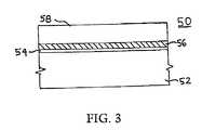
- FIG. 3shows a memory element 50 at a stage of the fabrication process known in the art.
- a first insulating layer 54has been formed on a substrate 52 , which can be made of a material such as a silicon substrate or a variety of other materials such as plastic.
- Insulating layer 54may be formed by any known deposition method, such as sputtering by chemical vapor deposition (CVD), plasma enhanced CVD (PECVS), or physical vapor deposition (PVD).
- First insulating layer 54may be formed of a conventional insulating oxide, such as silicon oxide (SiO 2 ), silicon nitride (Si 3 N 4 ), or any other low dielectric constant material.
- FIG. 3further provides a bottom electrode 56 formed over first insulating layer 54 .
- the bottom electrode 56preferably comprises tungsten, but may comprise any conductive material.
- a second insulating layer 58is formed over bottom electrode 56 , as shown in FIG. 3.
- the second insulating layer 58may comprise the same materials as first insulating layer 54 , such as SiO 2 and Si 3 N 4 .
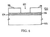
- an opening 60is formed in second insulating layer 58 to provide the structure shown in FIG. 4. Opening 60 may be formed by known methods in the art, such as a conventional patterning and etching process. Opening 60 is formed such that the surface of bottom electrode 56 is exposed in opening 60 . After the patterning and etch back process any masking material used is stripped away to leave the structure at a state represented in FIG. 4.
- a first chalcogenide glasspreferably a germanium-selenide glass layer 62 , is formed in opening 60 on top of bottom electrode 58 .
- the first germanium-selenide glass layer 62is preferably germanium-selenide of Ge x Se 100 ⁇ x stoichiometry. More preferably germanium-selenide glass layer 62 has formula Ge x Se 100 ⁇ x where x is between about 18 and about 33 or about 38 and about 43
- first germanium-selenide glass layer 62 having the preferred stoichiometric formulamay be accomplished by any appropriate method. Evaporation, co-sputtering germanium and selenium in appropriate ratios, sputtering using a germanium-selenide target having the desired stoichiometry, or chemical vapor deposition with stoichiometric amounts of GeH 4 and SeH 2 gases (or various compositions of these gases), which result in a germanium-selenide layer of the desired stoichiometry are methods which may be used to form germanium-selenide glass layer 62 . First germanium-selenide glass layer 62 is then planarized and etched back by techniques known in the art to provide a structure such as a that shown in FIG. 5.
- a metalpreferably silver is incorporated into the first germanium-selenide glass layer 62 at step 330 .
- a metalpreferably silver
- the method by which the metal is incorporated into the first germanium-selenide glass layer 62depends on the stoichiometry of the germanium-selenide glass.
- germanium-selenide glass layer having a stoichiometry of Ge x Se 100 ⁇ xthe value of x determines the method by which metal is incorporated into the germanium-selenide glass layer.
- metalmay be introduced into first germanium-selenide glass layer 62 by treatment with light irradiation.
- a metal-containing layer 64(preferably containing silver (Ag) or silver-selenide) is deposited over first germanium-selenide glass layer 62 .
- metal and metal-containing layer 64will be further described herein as silver and a silver-containing layer.
- the method of incorporating silver into germanium-selenide glass layer 62varies according to the silver-containing layer 64 utilized. Where silver-containing layer 64 is silver, for example, incorporation of silver into the first germanium-selenide glass layer 62 may be accomplished by irradiating the layers with light. The layers are irradiated for about 5 to 30 minutes at between about 1 mW/cm 2 to about 10 mW/cm 2 with electromagnetic radiation from a wavelength of about 200 nm to about 600 nm.
- the irradiation processbreaks Ge-Se and Se-Se bonds in the first germanium-selenide glass layer 62 , allowing Se from germanium-selenide layer 62 to combine with Ag provided in silver-containing layer 64 and forming silver-selenide first germanium-selenide glass layer 62 .
- irradiationmay be used in combination with a thermal process using a temperature of about 50° C. to about 350° C., and preferably about 110° C. for about 5 to about 15 minutes, and more preferably about 10 minutes. This heating drives silver from silver-containing layer 64 into first germanium-selenide glass layer 62 , which may provide an additional source of Ag to bond with Se after the light treatment. Removing excess silver-containing layer 64 from device 50 leaves a first silver-containing germanium-selenide glass layer 68 , as shown in FIG. 7. Other embodiments of the present invention may retain silver-containing layer 64 .
- first silver-containing germanium-selenide layer 68may alternatively be obtained by virtue of adjacent placement of germanium-selenide glass layer 62 and silver-containing layer 64 without the irradiation step described above.
- silvermay be introduced to the germanium-selenide glass layer by utilizing a silver-selenide layer as described above.
- a metal-chalcogenide layer 66is deposited on first germanium-selenide glass layer 62 .
- the metal chalcogenideincludes silver-selenide.
- the metal chalcogenide layer 66will be further described herein as a silver-selenide layer.
- Silver-selenide layer 66may be deposited by any suitable method known in the art, with dry plasma deposition (DPD) preferred. Silver-selenide migrates into first germanium-selenide glass layer 62 . Referring to FIG. 7A, this migration of silver into the germanium-selenide glass changes the composition of the first germanium-selenide glass layer to that of a first silver-containing germanium-selenide glass layer 68 . Silver-selenide layer 66 may then be removed by any method known in the art.
- DPDdry plasma deposition
- a second silver-containing germanium-selenide glass layeris subsequently formed in the present invention.
- a second chalcogenide glasspreferably a second germanium-selenide glass layer 70
- This second germanium-selenide glass layer 70preferably has a stoichiometry of Ge x Se 100 ⁇ x .
- the second germanium-selenide glass layer 70preferably has more of an open glass matrix than the first germanium-selenide glass layer 62 , i.e., the second germanium-selenide glass layer preferably contains a smaller proportion of germanium as demonstrated by a smaller value of x.
- One preferred embodimentincludes a first germanium-selenide glass layer 62 having a value of x of about 38 to about 43 (preferably with a value of x of about 40 ), and a second germanium-selenide glass layer 70 having a value of x of about 18 to about 33 with a value of about 25 preferable.
- This particular embodimentutilizes a first glass with a tight matrix and a second glass with an open matrix as defined by the value of x. It must be understood, however, that both glass can have open matrices and both can have tight matrices.
- a first germanium-selenide glass layer 62may be utilized that has a more open matrix than second germanium-selenide glass layer 70 .
- the present inventionrequires only that there be a diversity in the value of x between the first and second germanium-selenide glass layers 62 , 70 .
- the stoichiometry of second germanium-selenide glass layer 70 and its relative stoichiometry and glass matrix structure with respect to first germanium-selenide glass layer 62is wholly dependent on the desired electrical character of the PCRAM element.
- step 350 of FIG. 2silver is introduced into the second germanium-selenide glass layer 70 .
- Thismay be carried out in accordance with the description of step 330 where silver is introduced into the first germanium-selenide glass layer 62 .
- a second silver-containing layer 72is silver
- incorporation of silver into the second germanium-selenide glass layer 70may be accomplished by irradiating the layers with light, as described above. The thermal process described above may also be used with the irradiation process. Removing excess silver-containing layer 72 from device 50 leaves a second silver-containing germanium-selenide glass layer 74 , as shown in FIG. 10.
- Other embodiments of the present inventionmay retain silver-containing layer 72 .
- second silver-containing germanium-selenide layer 74may alternatively be obtained by virtue of adjacent placement of germanium-selenide glass layer 62 and silver-containing layer 64 without the irradiation step described above.
- xhas a value between about 38 and 43
- a silver-containing layer(preferably comprising silver-selenide) is deposited over second germanium-selenide glass layer 70 , and silver is allowed to migrate from the silver-containing layer to the second germanium-selenide glass layer 70 , as in step 330 .
- Either method of incorporating silver into the germanium-selenide glass layerresults in a second silver-containing germanium-selenide glass layer 74 , as shown in FIG. 10 (where silver-containing layer 72 has been stripped).
- an upper electrodeis deposited over the previous layer to form a semiconductor device 50 as shown in FIG. 11.
- the upper electrodeis preferably silver, but may comprise any suitable conductive material.
- the present inventionmay be utilized in any of a number of memory cell configurations known in the art.
- the memory cell 50 A shown in FIG. 11Ais provided where bottom electrode 56 is deposited in an opening formed in first insulating layer 54 , rather than on top of first insulating layer 54 , as shown in FIG. 11.
- the specific memory cell configurationwill vary according to the specific application of the desired memory cell by altering, among other factors, the deposition and etching processes employed.
- a second embodiment of the present inventionincludes forming at least one additional silver-containing germanium-selenide glass layer above second silver-containing germanium-selenide glass layer 74 .
- Thisis accomplished in the same way that second silver-containing germanium-selenide glass layer 74 is formed over first silver-containing germanium-selenide glass layer 68 .
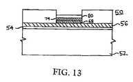
- a chalcogenide glasspreferably an additional germanium-selenide glass layer 80 , is deposited in opening 60 as shown in FIG. 13. This may be accomplished in the same ways that second germanium-selenide glass layer 70 is deposited at step 340 .
- the additional germanium-selenide glass layer 80preferably has a stoichiometry of Ge x Se 100 ⁇ x
- the additional germanium-selenide glass layer 80has a glass matrix structure distinct from any adjacently placed germanium-selenide glass layer, including second silver-containing germanium-selenide glass layer 74 in the case of a first additional silver-containing germanium-selenide glass layer.
- the additional germanium-selenide glass layer 80may have the same glass matrix structure as any germanium-selenide glass layer not adjacent to additional germanium-selenide glass layer 80 , such as first silver-containing germanium-selenide glass layer 68 .
- step 350 B of FIG. 12silver is introduced into the additional germanium-selenide glass layer 80 .
- Thismay be carried Out in accordance with the description of step 330 where silver is introduced into the first germanium-selenide glass layer 62 .
- an additional silver-containing layer 82is silver
- incorporation of silver into the additional germanium-selenide glass layer 80may be accomplished by irradiating the layers with light, as described above. The thermal process described above may also be used with the irradiation process. Removing excess silver-containing layer 82 from device 50 leaves an additional silver-containing germanium-selenide glass layer 84 , as shown in FIG. 15.
- Other embodiments of the present inventionmay retain silver-containing layer 82 .
- additional silver-containing germanium-selenide layer 84may alternatively be obtained by virtue of adjacent placement of additional germanium-selenide glass layer 80 and additional silver-containing layer 82 without the irradiation step described above.
- xhas a value between about 38 and 43
- a silver-containing layer(preferably comprising silver-selenide) is deposited over additional germanium-selenide glass layer 80 , and silver is allowed to migrate from the silver-containing layer to the additional germanium-selenide glass layer 80 , as in step 330 .
- Either method of incorporating silver into the germanium-selenide glass layerresults in an additional silver-containing germanium-selenide glass layer 84 , as shown in FIG. 15 (where silver-containing layer 82 has been stripped).
- an upper electrode 76is deposited over the previous layer (in this case 84 ) to form a semiconductor device 50 as shown in FIG. 16.
- the upper electrodeis preferably silver, but may comprise any suitable conductive material.
- one preferred embodiment of the memory element comprising at least one additional germanium-selenide layerincludes a first silver-containing germanium-selenide glass layer 68 having a value of x of about 38 to about 43 (preferably with a value of x of about 40), and a second silver-containing germanium-selenide glass layer 74 having a value of x of about 18 to about 33 with a value of about 25 preferable.
- the at least one additional silver-containing germanium-selenide layer 84has a value of x different from the value of x for the second silver-containing germanium-selenide glass layer 74 , and preferably from about 38 to about 43, more preferably 40, the same value as x for the first silver-containing germanium-selenide glass layer 68 .
- first silver-containing germanium-selenide glass layer 68 and additional silver-containing germanium-selenide glass layer 84have equal stoichiometries providing a tight glass matrix structure, while second silver-containing germanium-selenide glass layer 74 has a stoichiometry providing an open glass matrix structure.
- first silver-containing germanium-selenide glass layer 68 and additional silver-containing germanium-selenide glass layer 84have equal stoichiometries providing a tight glass matrix structure
- second silver-containing germanium-selenide glass layer 74has a stoichiometry providing an open glass matrix structure.
- first and second germanium-selenide glass layers 62 , 70need only have diverse values of x, without a requirement that the first germanium-selenide glass layer 62 have a higher value of x or a tighter glass matrix structure than second germanium-selenide glass layer 70 .
- the present inventionlikewise does not require that additional germanium-selenide glass layer 80 (and consequently additional silver-containing germanium-selenide glass layer 84 ) have any particular value of x or glass matrix structure.
- Additional silver-containing germanium-selenide glass layer 84must only have a value of x and a glass matrix structure different from adjacent silver-containing germanium-selenide glass layers, such as the second silver-containing germanium-selenide glass layer 74 .
- the memory cell 50 A shown in FIG. 16Ais provided where bottom electrode 56 is deposited in an opening formed in first insulating layer 54 , rather than on top of first insulating layer 54 , as shown in FIG. 16.
- the specific memory cell configurationwill vary according to the specific application of the desired memory cell by altering, among other factors, the deposition and etching processes employed.
- first and additional silver-containing germanium-selenide glass layers 68 , 84may have equal values of x providing more open glass matrix structure compared to second silver-containing germanium-selenide glass layer 74 having a more tight glass matrix structure.
- first silver-containing germanium-selenide glass layer 68may have a more tight glass matrix structure than second silver-containing germanium-selenide glass layer 74 , which in turn may have a more tight glass matrix structure than additional silver-containing germanium-selenide glass layer 84 , providing a stack of silver-containing germanium-selenide glass layers with descendingly graded stoichiometries. These values of x can be inverted to provide a stack of silver-containing germanium-selenide glass layers with ascendingly graded stoichiometries.
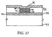
- FIG. 17provides four distinct silver-containing germanium-selenide glass layers 68 , 74 , 84 , and 86 .
- Stoichiometries which may be usedare those included in the above description of forming memory elements comprising at least one additional silver-containing germanium-selenide glass layer.
- bottom electrode 56is deposited in an opening formed in first insulating layer 54 , rather than on top of first insulating layer 54 , as shown in FIG. 17.
- the specific memory cell configurationwill vary according to the specific application of the desired memory cell by altering, among other factors, the deposition and etching processes employed.
- the combination of silver-containing germanium-selenide glass layers 68 , 74 (and 84 , 86 in embodiments comprising at least one additional silver-containing germanium-selenide glass layer)may be selected according to the desired electronic characteristics of the memory element being fabricated. Additionally, utilizing a relatively open-matrix germanium-selenide glass layers with tighter-matrix rigid glass layers provides increased adhesion between the glass and the semiconductor side walls. This is because a more open-matrix glass has greater ability to deform to surface defects and therefore provides greater surface area for contact. The increased presence of free selenium in open-matrix glass may also form bonds with side wall constituents such as silicon, thus aiding in adhesion.
- PCRAM performance with respect to both electrical characteristics and side wall adhesionwill vary depending on the germanium-selenide glass composition, the order of silver-containing germanium-selenide glass layers, and the number of silver-containing germanium-selenide glass layers. It should therefore be readily understood that the invention can be modified in these specific respects as well as to any number of variations, alterations, substitutions or equivalent arrangements not heretofore described, but which are commensurate with the spirit and scope of the invention in order to obtain a desired memory functionality. Accordingly, the invention is not to be seen as limited by the foregoing description, but is only limited by the scope of the appended claims.
Landscapes
- Engineering & Computer Science (AREA)
- Manufacturing & Machinery (AREA)
- Semiconductor Memories (AREA)
Abstract
Description
- 1. Field of the Invention[0001]
- The invention relates to the field of random access memory (RAM) devices formed using chalcogenide glass layers, and in particular to an improved programmable conductor random access memory (PCRAM) element design utilizing germanium-selenide glass layers.[0002]
- 2. Description of the Related Art[0003]
- Programmable conductor memory elements recently have been investigated for suitability as semi-volatile and non-volatile random access memory devices. One known PCRAM element composition utilizes a germanium-selenide chalcogenide glass of Ge[0004]xSe100−xstoichiometry. A metal, such as silver, is incorporated into the germanium-selenide glass. It is believed that the metal provides conductivity to the element thus allowing the element to be switched between two resistance states. Particularly, a silver-containing GexSe100−xglass layer is positioned between two electrodes utilized in a PCRAM element.
- The resistance of the silver-containing germanium-selenide glass layer can be changed between high resistance and low resistance states. The programmable conductor memory element is normally in a high resistance state when at rest. A write operation to a low resistance state is performed by applying a voltage potential across the two electrodes. When set in a low resistance state, the state of the memory element will remain intact for days or weeks after the voltage potentials are removed. The memory element can be returned to its high resistance state by applying a reverse voltage potential between the electrodes as used to write the element to the low resistance state. Again, the highly resistant state is maintained once the voltage potential is removed. This way, such a device can function, for example, as a resistance variable memory element having two resistance states, which can represent two logic states.[0005]
- The stoichiometry of a Ge[0006]xSe100−xglass inherently provides many different glass compositions depending on the value of x. Certain structural characteristics of GexSe100−xhave been observed with a change in the value of x. Specifically, referring now to prior art FIG. 1 (adapted from Boolchand, P., et al. “Onset of Rigidity in Steps in Chalcogenide Glasses—The Intermediate Phase” in M. Thorpe (ed.)Properties and Applications of Amorphous Materials, NATO Science Series (Plenum/Kluwer, 2001)), GexSe100−xglasses that are selenium-rich, i.e., glasses having a stoichiometry whereby x is less than or equal to 20, have a loose or open glass matrix as a result of the higher proportion of Se-Se bonds which occur when the relative number of germanium atoms is low. By contrast, GexSe100−xglass with values of x greater than 26 have a tight or rigid glass matrix due to the greater proportion of Ge-Se bonds present in the glass. GexSe100−xglass with values of x between 20 and 26 has an intermediate glass matrix. Rigidity is relative and based on the stoichiometry of the GexSe100−xglass. Accordingly, a Ge40Se60glass is more rigid than a Ge33Se67glass, and Ge25Se75glass is more rigid than Ge20Se80glass. Glass matrix structure is also relative and a function of the value of x. Therefore, a Ge40Se60glass has a tighter glass matrix structure than a Ge33Se67glass, and Ge25Se75glass has a tighter glass matrix structure than Ge20Se80glass.
- The structure of the glass matrix, i.e., tight versus open, affects the switching characteristics of the memory element. If the Ge[0007]xSe100−xglass has a tight matrix, then a larger resistance change is inhibited when a memory element switches from an on to an off state. On the other hand, if the germanium-selenide glass matrix is looser, or more open, then a larger resistance change is more easily facilitated. Accordingly, since glasses having a tight matrix inhibit a large resistance change, a PCRAM element utilizing a glass with a tight matrix will keep the programmed state longer than a PCRAM element utilizing a glass with an open matrix.
- While a PCRAM element comprised exclusively of a glass with an open matrix will be placed in a low resistance state or a high resistance state more quickly than a PCRAM element comprised exclusively of a glass with a tight matrix, glass with an open matrix used by itself is also not ideal. First, a PCRAM element utilizing glass with an open matrix may allow multiple low resistive pathways to be formed during programming. The tighter glass matrix will allow formation of a preferred conductive pathway with the properties of improved switching reliability and reduced resistance drift because there are fewer resistively decaying conductive pathways. Furthermore, the low melting point of selenium-rich glass, i.e., glass with an open matrix makes fabrication of PCRAM elements containing only glass with an open matrix difficult and complicated.[0008]
- What is needed is a design for a PCRAM element which provides faster operation and better data retention than that which can be obtained with either open-matrix or tight-matrix glass.[0009]
- The present invention provides a new structure for a PCRAM element which utilizes Ge[0010]xSe100−xglass layers of varying stoichiometry. The present invention additionally provides a method for making a PCRAM element comprising GexSe100−xglass layers of varying stoichiometry. In the preferred embodiment, the PCRAM element structure comprises a first electrode positioned beneath a first germanium-selenide glass layer with a stoichiometry providing a certain glass matrix structure. Located above this first germanium-selenide glass layer is a second germanium-selenide glass layer with a different stoichiometry providing a different glass matrix structure than the stoichiometry of the first germanium-selenide glass layer provides. A metal is introduced into each of these germanium-selenide glass layers. A second electrode is disposed on top of the second germanium-selenide glass layer.
- The preferred embodiment of the method of fabricating the present invention includes: forming an insulating layer over a first electrode; forming an opening in the insulating layer to expose a portion of the first electrode; forming a first germanium-selenide glass layer of a specific stoichiometry in the opening; introducing a metal into the first germanium-selenide glass layer; forming a second germanium-selenide glass layer of a stoichiometry different from that of the first germanium-selenide glass layer, and hence a different glass structure; introducing a metal into the second germanium-selenide glass layer; and forming a second electrode over the insulating layer and over the second metal-containing germanium-selenide glass layer.[0011]
- Additional advantages and features of the present invention will be apparent from the following detailed description provided in connection with the accompanying drawings which illustrate exemplary embodiments of the invention.[0012]
- FIG. 1 shows the values of x in the formula Ge[0013]xSe100−xwhich provide for an open matrix (“floppy”) and a tight matrix (“rigid”);
- FIG. 2 is a flowchart showing the steps of fabricating a memory element in accordance with the preferred embodiment of the present invention;[0014]
- FIG. 3 is a cross-sectional view of a semiconductor substrate having a first insulating layer, a bottom electrode and second insulating layer;[0015]
- FIG. 4 shows the substrate of FIG. 3 undergoing the process of the preferred embodiment of the present invention;[0016]
- FIG. 5 shows the substrate of FIG. 4 at a processing step subsequent to that shown in FIG. 4;[0017]
- FIG. 6 shows the substrate of FIG. 5 at a processing step subsequent to that shown in FIG. 5;[0018]
- FIG. 6A shows the substrate of FIG. 5 at an alternative processing step subsequent to that shown in FIG. 5;[0019]
- FIG. 7 shows the substrate of FIG. 6 at a processing step subsequent to that shown in FIG. 6;[0020]
- FIG. 7A shows the substrate of FIG. 6A at a processing step subsequent to that shown in FIG. 6A;[0021]
- FIG. 8 shows the substrate of FIG. 7 at a processing step subsequent to that shown in FIG. 7;[0022]
- FIG. 9 shows the substrate of FIG. 8 at a processing step subsequent to that shown in FIG. 8;[0023]
- FIG. 10 shows the substrate of FIG. 9 at a processing step subsequent to that shown in FIG. 9;[0024]
- FIG. 11 shows the substrate of FIG. 10 at a processing step subsequent to that shown in FIG. 10;[0025]
- FIG. 11A shows an alternative embodiment of the substrate shown in FIG. 11;[0026]
- FIG. 12 is a flowchart showing the steps of fabricating a memory element in accordance with a second preferred embodiment of the present invention;[0027]
- FIG. 13 shows the substrate of FIG. 10 undergoing the process of the second preferred embodiment of the present invention;[0028]
- FIG. 14 shows the substrate of FIG. 13 at a processing step subsequent to that shown in FIG. 13;[0029]
- FIG. 15 shows the substrate of FIG. 14 at a processing step subsequent to that shown in FIG. 14;[0030]
- FIG. 16 shows the substrate of FIG. 15 at a processing step subsequent to that shown in FIG. 15;[0031]
- FIG. 16A shows an alternative embodiment of the substrate shown in FIG. 16;[0032]
- FIG. 17 shows an additional memory element according to second preferred embodiment of the present invention;[0033]
- FIG. 17A shows and alternative embodiment of the substrate shown in FIG. 17.[0034]
- In the following description, reference is made to the accompanying drawings which will serve to illustrate exemplary embodiments of the invention. The description provides sufficient detail to enable those skilled in the art to practice the invention. Of course other embodiments may be used and various changes may be made without departing from the scope of the present invention. The scope of this invention is defined by the appended claims.[0035]
- The term “substrate” used in the following description may include any supporting structure including, but not limited to, a plastic or a semiconductor substrate that has an exposed substrate surface. Semiconductor substrates should be understood to include silicon, silicon-on-insulator (SOI), silicon-on-sapphire (SOS), doped and undoped semiconductors, epitaxial layers of silicon supported by a base semiconductor foundation, and other semiconductor structures. When reference is made to a semiconductor substrate or wafer in the following description, previous process steps may have been utilized to form regions or junctions in or over the base semiconductor or foundation.[0036]
- The term “silver” is intended to include not only elemental silver, but silver with other trace metals or in various alloyed combinations with other metals as known in the semiconductor industry, as long as such silver alloy is conductive, and as long as the physical and electrical properties of the silver remain unchanged.[0037]
- The term “silver-selenide” is intended to include various species of silver-selenide, including some species which have a slight excess or deficit of silver, for instance, Ag[0038]2Se, Ag2+xSe, and Ag2−xSe.
- The term “semi-volatile memory device” is intended to include any memory device which is capable of maintaining its memory state after power is removed from the device for a prolonged period of time. Thus, semi-volatile memory devices are capable of retaining stored data after the power source is disconnected or removed. The term “semi-volatile memory device” as used herein includes not only semi-volatile memory devices, but also non-volatile memory devices.[0039]
- FIG. 3 shows a[0040]
memory element 50 at a stage of the fabrication process known in the art. A first insulatinglayer 54 has been formed on asubstrate 52, which can be made of a material such as a silicon substrate or a variety of other materials such as plastic. Insulatinglayer 54 may be formed by any known deposition method, such as sputtering by chemical vapor deposition (CVD), plasma enhanced CVD (PECVS), or physical vapor deposition (PVD). First insulatinglayer 54 may be formed of a conventional insulating oxide, such as silicon oxide (SiO2), silicon nitride (Si3N4), or any other low dielectric constant material. FIG. 3 further provides abottom electrode 56 formed over first insulatinglayer 54. Thebottom electrode 56 preferably comprises tungsten, but may comprise any conductive material. - Using the FIG. 3 structure containing[0041]
bottom electrode 56 as a starting point and referring to the processing sequence shown in FIG. 2, a first embodiment of the invention will now be explained. Atstep 300 in FIG. 2, a second insulatinglayer 58 is formed overbottom electrode 56, as shown in FIG. 3. The second insulatinglayer 58 may comprise the same materials as first insulatinglayer 54, such as SiO2and Si3N4. Atstep 310 anopening 60 is formed in second insulatinglayer 58 to provide the structure shown in FIG. 4.Opening 60 may be formed by known methods in the art, such as a conventional patterning and etching process.Opening 60 is formed such that the surface ofbottom electrode 56 is exposed inopening 60. After the patterning and etch back process any masking material used is stripped away to leave the structure at a state represented in FIG. 4. - At step[0042]320 a first chalcogenide glass, preferably a germanium-
selenide glass layer 62, is formed in opening60 on top ofbottom electrode 58. The first germanium-selenide glass layer 62 is preferably germanium-selenide of GexSe100−xstoichiometry. More preferably germanium-selenide glass layer 62 has formula GexSe100−xwhere x is between about 18 and about 33 or about 38 and about 43 - The formation of the first germanium-[0043]
selenide glass layer 62 having the preferred stoichiometric formula may be accomplished by any appropriate method. Evaporation, co-sputtering germanium and selenium in appropriate ratios, sputtering using a germanium-selenide target having the desired stoichiometry, or chemical vapor deposition with stoichiometric amounts of GeH4and SeH2gases (or various compositions of these gases), which result in a germanium-selenide layer of the desired stoichiometry are methods which may be used to form germanium-selenide glass layer 62. First germanium-selenide glass layer 62 is then planarized and etched back by techniques known in the art to provide a structure such as a that shown in FIG. 5. - Referring back to FIG. 2, a metal, preferably silver, is incorporated into the first germanium-[0044]
selenide glass layer 62 atstep 330. Preferably, about 1% to about 10% less than the maximum amount of silver necessary to keep first germanium-selenide glass layer 62 in an amorphous state is ultimately incorporated into the glass layer, totaling less than or equal to about 33% of the glass layer. The method by which the metal is incorporated into the first germanium-selenide glass layer 62 depends on the stoichiometry of the germanium-selenide glass. For example, when a germanium-selenide glass layer having a stoichiometry of GexSe100−xthe value of x determines the method by which metal is incorporated into the germanium-selenide glass layer. For germanium-selenide glass of formula GexSe100−xwhere x is less than or equal to 33, for example, metal may be introduced into first germanium-selenide glass layer 62 by treatment with light irradiation. - Specifically, referring now to FIG. 6, a metal-containing layer[0045]64 (preferably containing silver (Ag) or silver-selenide) is deposited over first germanium-
selenide glass layer 62. For purposes of simplified discussion, metal and metal-containinglayer 64 will be further described herein as silver and a silver-containing layer. - The method of incorporating silver into germanium-[0046]
selenide glass layer 62 varies according to the silver-containinglayer 64 utilized. Where silver-containinglayer 64 is silver, for example, incorporation of silver into the first germanium-selenide glass layer 62 may be accomplished by irradiating the layers with light. The layers are irradiated for about 5 to 30 minutes at between about 1 mW/cm2to about 10 mW/cm2with electromagnetic radiation from a wavelength of about 200 nm to about 600 nm. The irradiation process breaks Ge-Se and Se-Se bonds in the first germanium-selenide glass layer 62, allowing Se from germanium-selenide layer 62 to combine with Ag provided in silver-containinglayer 64 and forming silver-selenide first germanium-selenide glass layer 62. In addition, irradiation may be used in combination with a thermal process using a temperature of about 50° C. to about 350° C., and preferably about 110° C. for about 5 to about 15 minutes, and more preferably about 10 minutes. This heating drives silver from silver-containinglayer 64 into first germanium-selenide glass layer 62, which may provide an additional source of Ag to bond with Se after the light treatment. Removing excess silver-containinglayer 64 fromdevice 50 leaves a first silver-containing germanium-selenide glass layer 68, as shown in FIG. 7. Other embodiments of the present invention may retain silver-containinglayer 64. - Referring back to FIG. 6, if silver-containing[0047]
layer 64 is silver-selenide, first silver-containing germanium-selenide layer 68 may alternatively be obtained by virtue of adjacent placement of germanium-selenide glass layer 62 and silver-containinglayer 64 without the irradiation step described above. - For embodiments of the present invention utilizing a first germanium-[0048]
selenide glass layer 62 with GexSe100−xstoichiometry and x between about 38 and about43, silver may be introduced to the germanium-selenide glass layer by utilizing a silver-selenide layer as described above. Specifically, referring now to FIG. 6A, a metal-chalcogenide layer 66 is deposited on first germanium-selenide glass layer 62. Preferably the metal chalcogenide includes silver-selenide. For the purposes of simplified discussion, themetal chalcogenide layer 66 will be further described herein as a silver-selenide layer. Silver-selenide layer 66 may be deposited by any suitable method known in the art, with dry plasma deposition (DPD) preferred. Silver-selenide migrates into first germanium-selenide glass layer 62. Referring to FIG. 7A, this migration of silver into the germanium-selenide glass changes the composition of the first germanium-selenide glass layer to that of a first silver-containing germanium-selenide glass layer 68. Silver-selenide layer 66 may then be removed by any method known in the art. - Regardless of which method is employed to incorporate silver into first germanium-[0049]
selenide glass layer 62 to form a first silver-containing germanium-selenide glass layer 68, a second silver-containing germanium-selenide glass layer is subsequently formed in the present invention. Referring to FIG. 2, at step340 a second chalcogenide glass, preferably a second germanium-selenide glass layer 70, is deposited in opening60, as shown in FIG. 8. This may be accomplished in the same ways that first germanium-selenide glass layer 62 is deposited atstep 320. This second germanium-selenide glass layer 70 preferably has a stoichiometry of GexSe100−x. The second germanium-selenide glass layer 70 preferably has more of an open glass matrix than the first germanium-selenide glass layer 62, i.e., the second germanium-selenide glass layer preferably contains a smaller proportion of germanium as demonstrated by a smaller value of x. - One preferred embodiment includes a first germanium-[0050]
selenide glass layer 62 having a value of x of about 38 to about 43 (preferably with a value of x of about40), and a second germanium-selenide glass layer 70 having a value of x of about 18 to about 33 with a value of about 25 preferable. This particular embodiment utilizes a first glass with a tight matrix and a second glass with an open matrix as defined by the value of x. It must be understood, however, that both glass can have open matrices and both can have tight matrices. In addition, a first germanium-selenide glass layer 62 may be utilized that has a more open matrix than second germanium-selenide glass layer 70. The present invention requires only that there be a diversity in the value of x between the first and second germanium-selenide glass layers62,70. As with first germanium-selenide glass layer 62, the stoichiometry of second germanium-selenide glass layer 70 and its relative stoichiometry and glass matrix structure with respect to first germanium-selenide glass layer 62 is wholly dependent on the desired electrical character of the PCRAM element. - At[0051]
step 350 of FIG. 2 silver is introduced into the second germanium-selenide glass layer 70. This may be carried out in accordance with the description ofstep 330 where silver is introduced into the first germanium-selenide glass layer 62. Referring to FIG. 8 and FIG. 9, where a second silver-containing layer72 is silver, for example, incorporation of silver into the second germanium-selenide glass layer 70 may be accomplished by irradiating the layers with light, as described above. The thermal process described above may also be used with the irradiation process. Removing excess silver-containing layer72 fromdevice 50 leaves a second silver-containing germanium-selenide glass layer 74, as shown in FIG. 10. Other embodiments of the present invention may retain silver-containing layer72. - Referring back to FIG. 9, if second silver-containing layer[0052]72 is silver-selenide, second silver-containing germanium-
selenide layer 74 may alternatively be obtained by virtue of adjacent placement of germanium-selenide glass layer 62 and silver-containinglayer 64 without the irradiation step described above. Where x has a value between about 38 and 43, a silver-containing layer (preferably comprising silver-selenide) is deposited over second germanium-selenide glass layer 70, and silver is allowed to migrate from the silver-containing layer to the second germanium-selenide glass layer 70, as instep 330. - Either method of incorporating silver into the germanium-selenide glass layer results in a second silver-containing germanium-[0053]
selenide glass layer 74, as shown in FIG. 10 (where silver-containing layer72 has been stripped). Atstep 360, an upper electrode is deposited over the previous layer to form asemiconductor device 50 as shown in FIG. 11. The upper electrode is preferably silver, but may comprise any suitable conductive material. - It should be recognized that the present invention may be utilized in any of a number of memory cell configurations known in the art. For example, the[0054]
memory cell 50A shown in FIG. 11A is provided wherebottom electrode 56 is deposited in an opening formed in first insulatinglayer 54, rather than on top of first insulatinglayer 54, as shown in FIG. 11. The specific memory cell configuration will vary according to the specific application of the desired memory cell by altering, among other factors, the deposition and etching processes employed. - Referring now to FIG. 12, a second embodiment of the present invention includes forming at least one additional silver-containing germanium-selenide glass layer above second silver-containing germanium-[0055]
selenide glass layer 74. This is accomplished in the same way that second silver-containing germanium-selenide glass layer 74 is formed over first silver-containing germanium-selenide glass layer 68. Specifically, atstep 350A, a chalcogenide glass, preferably an additional germanium-selenide glass layer80, is deposited in opening60 as shown in FIG. 13. This may be accomplished in the same ways that second germanium-selenide glass layer 70 is deposited atstep 340. The additional germanium-selenide glass layer80 preferably has a stoichiometry of GexSe100−xThe additional germanium-selenide glass layer80 has a glass matrix structure distinct from any adjacently placed germanium-selenide glass layer, including second silver-containing germanium-selenide glass layer 74 in the case of a first additional silver-containing germanium-selenide glass layer. The additional germanium-selenide glass layer80 may have the same glass matrix structure as any germanium-selenide glass layer not adjacent to additional germanium-selenide glass layer80, such as first silver-containing germanium-selenide glass layer 68. - At[0056]
step 350B of FIG. 12, silver is introduced into the additional germanium-selenide glass layer80. This may be carried Out in accordance with the description ofstep 330 where silver is introduced into the first germanium-selenide glass layer 62. Referring to FIG. 8 and FIG. 9, where an additional silver-containinglayer 82 is silver, for example, incorporation of silver into the additional germanium-selenide glass layer80 may be accomplished by irradiating the layers with light, as described above. The thermal process described above may also be used with the irradiation process. Removing excess silver-containinglayer 82 fromdevice 50 leaves an additional silver-containing germanium-selenide glass layer 84, as shown in FIG. 15. Other embodiments of the present invention may retain silver-containinglayer 82. - Referring back to FIG. 14, if additional silver-containing[0057]
layer 82 is silver-selenide, additional silver-containing germanium-selenide layer 84 may alternatively be obtained by virtue of adjacent placement of additional germanium-selenide glass layer80 and additional silver-containinglayer 82 without the irradiation step described above. Where x has a value between about 38 and 43, a silver-containing layer (preferably comprising silver-selenide) is deposited over additional germanium-selenide glass layer80, and silver is allowed to migrate from the silver-containing layer to the additional germanium-selenide glass layer80, as instep 330. Either method of incorporating silver into the germanium-selenide glass layer results in an additional silver-containing germanium-selenide glass layer 84, as shown in FIG. 15 (where silver-containinglayer 82 has been stripped). - At[0058]
step 360, anupper electrode 76 is deposited over the previous layer (in this case84) to form asemiconductor device 50 as shown in FIG. 16. The upper electrode is preferably silver, but may comprise any suitable conductive material. - Referring to FIG. 16, one preferred embodiment of the memory element comprising at least one additional germanium-selenide layer includes a first silver-containing germanium-[0059]
selenide glass layer 68 having a value of x of about 38 to about 43 (preferably with a value of x of about 40), and a second silver-containing germanium-selenide glass layer 74 having a value of x of about 18 to about 33 with a value of about 25 preferable. The at least one additional silver-containing germanium-selenide layer 84 has a value of x different from the value of x for the second silver-containing germanium-selenide glass layer 74, and preferably from about 38 to about 43, more preferably 40, the same value as x for the first silver-containing germanium-selenide glass layer 68. - In the resulting memory element, first silver-containing germanium-[0060]
selenide glass layer 68 and additional silver-containing germanium-selenide glass layer 84 have equal stoichiometries providing a tight glass matrix structure, while second silver-containing germanium-selenide glass layer 74 has a stoichiometry providing an open glass matrix structure. However, as discussed above with reference to the first embodiment of the present invention, and FIG. 5 and FIG. 8, first and second germanium-selenide glass layers62,70 (and consequently first and second silver-containing germanium-selenide layers 68,74) need only have diverse values of x, without a requirement that the first germanium-selenide glass layer 62 have a higher value of x or a tighter glass matrix structure than second germanium-selenide glass layer 70. The present invention likewise does not require that additional germanium-selenide glass layer80 (and consequently additional silver-containing germanium-selenide glass layer84) have any particular value of x or glass matrix structure. Additional silver-containing germanium-selenide glass layer 84 must only have a value of x and a glass matrix structure different from adjacent silver-containing germanium-selenide glass layers, such as the second silver-containing germanium-selenide glass layer 74. - As with FIG. 11A, the[0061]
memory cell 50A shown in FIG. 16A is provided wherebottom electrode 56 is deposited in an opening formed in first insulatinglayer 54, rather than on top of first insulatinglayer 54, as shown in FIG. 16. The specific memory cell configuration will vary according to the specific application of the desired memory cell by altering, among other factors, the deposition and etching processes employed. - Referring to FIG. 16, this allows for many embodiments provided by the present invention. For example, in addition to the previously disclosed embodiment where first and additional silver-containing germanium-selenide glass layers[0062]68,84 had equal values of x providing tighter glass matrix structures and second silver-containing germanium-
selenide glass layer 74 had a more open glass structure, first and additional silver-containing germanium-selenide glass layers68,84 may have equal values of x providing more open glass matrix structure compared to second silver-containing germanium-selenide glass layer 74 having a more tight glass matrix structure. Furthermore, first silver-containing germanium-selenide glass layer 68 may have a more tight glass matrix structure than second silver-containing germanium-selenide glass layer 74, which in turn may have a more tight glass matrix structure than additional silver-containing germanium-selenide glass layer 84, providing a stack of silver-containing germanium-selenide glass layers with descendingly graded stoichiometries. These values of x can be inverted to provide a stack of silver-containing germanium-selenide glass layers with ascendingly graded stoichiometries. - It should be readily apparent to a person of ordinary skill in the art that the present invention provides many combinations of silver-containing germanium-selenide stacks for use in memory fabrication. Referring now to FIG. 17, it is clear that a memory element fabricated according to the present invention also is not limited in the number of silver-containing germanium-selenide layers included. FIG. 17 provides four distinct silver-containing germanium-selenide glass layers[0063]68,74,84, and86. Stoichiometries which may be used are those included in the above description of forming memory elements comprising at least one additional silver-containing germanium-selenide glass layer. As with FIG. 11A and FIG. 16A above,
memory cell 50A shown in FIG. 17A is provided wherebottom electrode 56 is deposited in an opening formed in first insulatinglayer 54, rather than on top of first insulatinglayer 54, as shown in FIG. 17. The specific memory cell configuration will vary according to the specific application of the desired memory cell by altering, among other factors, the deposition and etching processes employed. - The combination of silver-containing germanium-selenide glass layers[0064]68,74 (and84,86 in embodiments comprising at least one additional silver-containing germanium-selenide glass layer) may be selected according to the desired electronic characteristics of the memory element being fabricated. Additionally, utilizing a relatively open-matrix germanium-selenide glass layers with tighter-matrix rigid glass layers provides increased adhesion between the glass and the semiconductor side walls. This is because a more open-matrix glass has greater ability to deform to surface defects and therefore provides greater surface area for contact. The increased presence of free selenium in open-matrix glass may also form bonds with side wall constituents such as silicon, thus aiding in adhesion.
- PCRAM performance with respect to both electrical characteristics and side wall adhesion will vary depending on the germanium-selenide glass composition, the order of silver-containing germanium-selenide glass layers, and the number of silver-containing germanium-selenide glass layers. It should therefore be readily understood that the invention can be modified in these specific respects as well as to any number of variations, alterations, substitutions or equivalent arrangements not heretofore described, but which are commensurate with the spirit and scope of the invention in order to obtain a desired memory functionality. Accordingly, the invention is not to be seen as limited by the foregoing description, but is only limited by the scope of the appended claims.[0065]
Claims (70)
Priority Applications (2)
| Application Number | Priority Date | Filing Date | Title |
|---|---|---|---|
| US10/787,121US6953720B2 (en) | 2002-08-29 | 2004-02-27 | Methods for forming chalcogenide glass-based memory elements |
| US11/195,642US7518212B2 (en) | 2002-08-29 | 2005-08-03 | Graded GexSe100-x concentration in PCRAM |
Applications Claiming Priority (2)
| Application Number | Priority Date | Filing Date | Title |
|---|---|---|---|
| US10/230,327US6856002B2 (en) | 2002-08-29 | 2002-08-29 | Graded GexSe100-x concentration in PCRAM |
| US10/787,121US6953720B2 (en) | 2002-08-29 | 2004-02-27 | Methods for forming chalcogenide glass-based memory elements |
Related Parent Applications (1)
| Application Number | Title | Priority Date | Filing Date |
|---|---|---|---|
| US10/230,327DivisionUS6856002B2 (en) | 2002-08-29 | 2002-08-29 | Graded GexSe100-x concentration in PCRAM |
Related Child Applications (1)
| Application Number | Title | Priority Date | Filing Date |
|---|---|---|---|
| US11/195,642ContinuationUS7518212B2 (en) | 2002-08-29 | 2005-08-03 | Graded GexSe100-x concentration in PCRAM |
Publications (2)
| Publication Number | Publication Date |
|---|---|
| US20040185625A1true US20040185625A1 (en) | 2004-09-23 |
| US6953720B2 US6953720B2 (en) | 2005-10-11 |
Family
ID=31990383
Family Applications (3)
| Application Number | Title | Priority Date | Filing Date |
|---|---|---|---|
| US10/230,327Expired - LifetimeUS6856002B2 (en) | 2002-08-29 | 2002-08-29 | Graded GexSe100-x concentration in PCRAM |
| US10/787,121Expired - LifetimeUS6953720B2 (en) | 2002-08-29 | 2004-02-27 | Methods for forming chalcogenide glass-based memory elements |
| US11/195,642Expired - LifetimeUS7518212B2 (en) | 2002-08-29 | 2005-08-03 | Graded GexSe100-x concentration in PCRAM |
Family Applications Before (1)
| Application Number | Title | Priority Date | Filing Date |
|---|---|---|---|
| US10/230,327Expired - LifetimeUS6856002B2 (en) | 2002-08-29 | 2002-08-29 | Graded GexSe100-x concentration in PCRAM |
Family Applications After (1)
| Application Number | Title | Priority Date | Filing Date |
|---|---|---|---|
| US11/195,642Expired - LifetimeUS7518212B2 (en) | 2002-08-29 | 2005-08-03 | Graded GexSe100-x concentration in PCRAM |
Country Status (1)
| Country | Link |
|---|---|
| US (3) | US6856002B2 (en) |
Families Citing this family (32)
| Publication number | Priority date | Publication date | Assignee | Title |
|---|---|---|---|---|
| US6881623B2 (en)* | 2001-08-29 | 2005-04-19 | Micron Technology, Inc. | Method of forming chalcogenide comprising devices, method of forming a programmable memory cell of memory circuitry, and a chalcogenide comprising device |
| US7319057B2 (en)* | 2001-10-30 | 2008-01-15 | Ovonyx, Inc. | Phase change material memory device |
| US6856002B2 (en)* | 2002-08-29 | 2005-02-15 | Micron Technology, Inc. | Graded GexSe100-x concentration in PCRAM |
| US7115927B2 (en) | 2003-02-24 | 2006-10-03 | Samsung Electronics Co., Ltd. | Phase changeable memory devices |
| US7425735B2 (en)* | 2003-02-24 | 2008-09-16 | Samsung Electronics Co., Ltd. | Multi-layer phase-changeable memory devices |
| DE102004025615B4 (en)* | 2004-05-25 | 2008-09-04 | Qimonda Ag | Method for producing a solid electrolyte memory cell |
| US7190048B2 (en)* | 2004-07-19 | 2007-03-13 | Micron Technology, Inc. | Resistance variable memory device and method of fabrication |
| EP1675183A1 (en)* | 2004-12-21 | 2006-06-28 | STMicroelectronics S.r.l. | Phase change memory cell with diode junction selection and manufacturing method thereof |
| KR100650753B1 (en)* | 2005-06-10 | 2006-11-27 | 주식회사 하이닉스반도체 | Phase change memory device and manufacturing method thereof |
| KR100637235B1 (en)* | 2005-08-26 | 2006-10-20 | 삼성에스디아이 주식회사 | Plasma display panel |
| KR100682952B1 (en)* | 2005-08-31 | 2007-02-15 | 삼성전자주식회사 | Nanoelastic memory device and manufacturing method thereof |
| US7973384B2 (en)* | 2005-11-02 | 2011-07-05 | Qimonda Ag | Phase change memory cell including multiple phase change material portions |
| US7723712B2 (en)* | 2006-03-17 | 2010-05-25 | Micron Technology, Inc. | Reduced power consumption phase change memory and methods for forming the same |
| KR100782482B1 (en)* | 2006-05-19 | 2007-12-05 | 삼성전자주식회사 | A phase change memory cell employing a thin film as a phase change material film, a phase change memory device having the same, an electronic device having the same, and a manufacturing method thereof |
| US7825033B2 (en)* | 2006-06-09 | 2010-11-02 | Micron Technology, Inc. | Methods of forming variable resistance memory cells, and methods of etching germanium, antimony, and tellurium-comprising materials |
| WO2008088599A2 (en) | 2006-10-19 | 2008-07-24 | Boise State University | Forced ion migration for chalcogenide phase change memory device |
| KR20080095683A (en)* | 2007-04-25 | 2008-10-29 | 삼성전자주식회사 | Phase change memory device and method of forming the same |
| US8373148B2 (en)* | 2007-04-26 | 2013-02-12 | Spansion Llc | Memory device with improved performance |
| KR100883412B1 (en)* | 2007-05-09 | 2009-02-11 | 삼성전자주식회사 | Method for manufacturing phase change memory device having self-aligned electrode, related device and electronic system |
| KR100881055B1 (en)* | 2007-06-20 | 2009-01-30 | 삼성전자주식회사 | Phase change memory unit, manufacturing method thereof, phase change memory device including same and manufacturing method thereof |
| FR2922368A1 (en)* | 2007-10-16 | 2009-04-17 | Commissariat Energie Atomique | METHOD FOR MANUFACTURING A CBRAM MEMORY HAVING IMPROVED RELIABILITY |
| FR2934711B1 (en)* | 2008-07-29 | 2011-03-11 | Commissariat Energie Atomique | MEMORY DEVICE AND CBRAM MEMORY WITH IMPROVED RELIABILITY. |
| US8467236B2 (en) | 2008-08-01 | 2013-06-18 | Boise State University | Continuously variable resistor |
| US8238146B2 (en)* | 2008-08-01 | 2012-08-07 | Boise State University | Variable integrated analog resistor |
| US7825479B2 (en) | 2008-08-06 | 2010-11-02 | International Business Machines Corporation | Electrical antifuse having a multi-thickness dielectric layer |
| US20110079709A1 (en)* | 2009-10-07 | 2011-04-07 | Campbell Kristy A | Wide band sensor |
| US8284590B2 (en) | 2010-05-06 | 2012-10-09 | Boise State University | Integratable programmable capacitive device |
| US8624217B2 (en) | 2010-06-25 | 2014-01-07 | International Business Machines Corporation | Planar phase-change memory cell with parallel electrical paths |
| US8575008B2 (en) | 2010-08-31 | 2013-11-05 | International Business Machines Corporation | Post-fabrication self-aligned initialization of integrated devices |
| KR101431656B1 (en)* | 2013-04-05 | 2014-08-21 | 한국과학기술연구원 | Chacogenide switching device using germanium and selenium and manufacture method thereof |
| US9583699B2 (en) | 2015-06-01 | 2017-02-28 | Boise State University | Tunable variable resistance memory device |
| US9583703B2 (en) | 2015-06-01 | 2017-02-28 | Boise State University | Tunable variable resistance memory device |
Citations (87)
| Publication number | Priority date | Publication date | Assignee | Title |
|---|---|---|---|---|
| US666A (en)* | 1838-04-02 | Sfbing-bock for coagh and railroad-gab | ||
| US168820A (en)* | 1875-10-11 | Improvement in violins | ||
| US3271591A (en)* | 1963-09-20 | 1966-09-06 | Energy Conversion Devices Inc | Symmetrical current controlling device |
| US3961314A (en)* | 1974-03-05 | 1976-06-01 | Energy Conversion Devices, Inc. | Structure and method for producing an image |
| US3966317A (en)* | 1974-04-08 | 1976-06-29 | Energy Conversion Devices, Inc. | Dry process production of archival microform records from hard copy |
| US3983542A (en)* | 1970-08-13 | 1976-09-28 | Energy Conversion Devices, Inc. | Method and apparatus for recording information |
| US4267261A (en)* | 1971-07-15 | 1981-05-12 | Energy Conversion Devices, Inc. | Method for full format imaging |
| US4597162A (en)* | 1983-01-18 | 1986-07-01 | Energy Conversion Devices, Inc. | Method for making, parallel preprogramming or field programming of electronic matrix arrays |
| US4608296A (en)* | 1983-12-06 | 1986-08-26 | Energy Conversion Devices, Inc. | Superconducting films and devices exhibiting AC to DC conversion |
| US4637895A (en)* | 1985-04-01 | 1987-01-20 | Energy Conversion Devices, Inc. | Gas mixtures for the vapor deposition of semiconductor material |
| US4646266A (en)* | 1984-09-28 | 1987-02-24 | Energy Conversion Devices, Inc. | Programmable semiconductor structures and methods for using the same |
| US4664939A (en)* | 1985-04-01 | 1987-05-12 | Energy Conversion Devices, Inc. | Vertical semiconductor processor |
| US4668968A (en)* | 1984-05-14 | 1987-05-26 | Energy Conversion Devices, Inc. | Integrated circuit compatible thin film field effect transistor and method of making same |
| US4670763A (en)* | 1984-05-14 | 1987-06-02 | Energy Conversion Devices, Inc. | Thin film field effect transistor |
| US4673957A (en)* | 1984-05-14 | 1987-06-16 | Energy Conversion Devices, Inc. | Integrated circuit compatible thin film field effect transistor and method of making same |
| US4678679A (en)* | 1984-06-25 | 1987-07-07 | Energy Conversion Devices, Inc. | Continuous deposition of activated process gases |
| US4728406A (en)* | 1986-08-18 | 1988-03-01 | Energy Conversion Devices, Inc. | Method for plasma - coating a semiconductor body |
| US4737379A (en)* | 1982-09-24 | 1988-04-12 | Energy Conversion Devices, Inc. | Plasma deposited coatings, and low temperature plasma method of making same |
| US4766471A (en)* | 1986-01-23 | 1988-08-23 | Energy Conversion Devices, Inc. | Thin film electro-optical devices |
| US4769338A (en)* | 1984-05-14 | 1988-09-06 | Energy Conversion Devices, Inc. | Thin film field effect transistor and method of making same |
| US4775425A (en)* | 1987-07-27 | 1988-10-04 | Energy Conversion Devices, Inc. | P and n-type microcrystalline semiconductor alloy material including band gap widening elements, devices utilizing same |
| US4809044A (en)* | 1986-08-22 | 1989-02-28 | Energy Conversion Devices, Inc. | Thin film overvoltage protection devices |
| US4818717A (en)* | 1986-06-27 | 1989-04-04 | Energy Conversion Devices, Inc. | Method for making electronic matrix arrays |
| US4843443A (en)* | 1984-05-14 | 1989-06-27 | Energy Conversion Devices, Inc. | Thin film field effect transistor and method of making same |
| US4845533A (en)* | 1986-08-22 | 1989-07-04 | Energy Conversion Devices, Inc. | Thin film electrical devices with amorphous carbon electrodes and method of making same |
| US4853785A (en)* | 1986-10-15 | 1989-08-01 | Energy Conversion Devices, Inc. | Electronic camera including electronic signal storage cartridge |
| US4891330A (en)* | 1987-07-27 | 1990-01-02 | Energy Conversion Devices, Inc. | Method of fabricating n-type and p-type microcrystalline semiconductor alloy material including band gap widening elements |
| US5128099A (en)* | 1991-02-15 | 1992-07-07 | Energy Conversion Devices, Inc. | Congruent state changeable optical memory material and device |
| US5159661A (en)* | 1990-10-05 | 1992-10-27 | Energy Conversion Devices, Inc. | Vertically interconnected parallel distributed processor |
| US5296716A (en)* | 1991-01-18 | 1994-03-22 | Energy Conversion Devices, Inc. | Electrically erasable, directly overwritable, multibit single cell memory elements and arrays fabricated therefrom |
| US5335219A (en)* | 1991-01-18 | 1994-08-02 | Ovshinsky Stanford R | Homogeneous composition of microcrystalline semiconductor material, semiconductor devices and directly overwritable memory elements fabricated therefrom, and arrays fabricated from the memory elements |
| US5341328A (en)* | 1991-01-18 | 1994-08-23 | Energy Conversion Devices, Inc. | Electrically erasable memory elements having reduced switching current requirements and increased write/erase cycle life |
| US5359205A (en)* | 1991-11-07 | 1994-10-25 | Energy Conversion Devices, Inc. | Electrically erasable memory elements characterized by reduced current and improved thermal stability |
| US5406509A (en)* | 1991-01-18 | 1995-04-11 | Energy Conversion Devices, Inc. | Electrically erasable, directly overwritable, multibit single cell memory elements and arrays fabricated therefrom |
| US5414271A (en)* | 1991-01-18 | 1995-05-09 | Energy Conversion Devices, Inc. | Electrically erasable memory elements having improved set resistance stability |
| US5500532A (en)* | 1994-08-18 | 1996-03-19 | Arizona Board Of Regents | Personal electronic dosimeter |
| US5534712A (en)* | 1991-01-18 | 1996-07-09 | Energy Conversion Devices, Inc. | Electrically erasable memory elements characterized by reduced current and improved thermal stability |
| US5534711A (en)* | 1991-01-18 | 1996-07-09 | Energy Conversion Devices, Inc. | Electrically erasable, directly overwritable, multibit single cell memory elements and arrays fabricated therefrom |
| US5536947A (en)* | 1991-01-18 | 1996-07-16 | Energy Conversion Devices, Inc. | Electrically erasable, directly overwritable, multibit single cell memory element and arrays fabricated therefrom |
| US5543737A (en)* | 1995-02-10 | 1996-08-06 | Energy Conversion Devices, Inc. | Logical operation circuit employing two-terminal chalcogenide switches |
| US5591501A (en)* | 1995-12-20 | 1997-01-07 | Energy Conversion Devices, Inc. | Optical recording medium having a plurality of discrete phase change data recording points |
| US5596522A (en)* | 1991-01-18 | 1997-01-21 | Energy Conversion Devices, Inc. | Homogeneous compositions of microcrystalline semiconductor material, semiconductor devices and directly overwritable memory elements fabricated therefrom, and arrays fabricated from the memory elements |
| US5714768A (en)* | 1995-10-24 | 1998-02-03 | Energy Conversion Devices, Inc. | Second-layer phase change memory array on top of a logic device |
| US5751012A (en)* | 1995-06-07 | 1998-05-12 | Micron Technology, Inc. | Polysilicon pillar diode for use in a non-volatile memory cell |
| US5761115A (en)* | 1996-05-30 | 1998-06-02 | Axon Technologies Corporation | Programmable metallization cell structure and method of making same |
| US5789277A (en)* | 1996-07-22 | 1998-08-04 | Micron Technology, Inc. | Method of making chalogenide memory device |
| US5825046A (en)* | 1996-10-28 | 1998-10-20 | Energy Conversion Devices, Inc. | Composite memory material comprising a mixture of phase-change memory material and dielectric material |
| US5912839A (en)* | 1998-06-23 | 1999-06-15 | Energy Conversion Devices, Inc. | Universal memory element and method of programming same |
| US5933365A (en)* | 1997-06-19 | 1999-08-03 | Energy Conversion Devices, Inc. | Memory element with energy control mechanism |
| US6011757A (en)* | 1998-01-27 | 2000-01-04 | Ovshinsky; Stanford R. | Optical recording media having increased erasability |
| US6087674A (en)* | 1996-10-28 | 2000-07-11 | Energy Conversion Devices, Inc. | Memory element with memory material comprising phase-change material and dielectric material |
| USRE37259E1 (en)* | 1996-04-19 | 2001-07-03 | Energy Conversion Devices, Inc. | Multibit single cell memory element having tapered contact |
| US6339544B1 (en)* | 2000-09-29 | 2002-01-15 | Intel Corporation | Method to enhance performance of thermal resistor device |
| US6348365B1 (en)* | 2001-03-02 | 2002-02-19 | Micron Technology, Inc. | PCRAM cell manufacturing |
| US6388324B2 (en)* | 1998-08-31 | 2002-05-14 | Arizona Board Of Regents | Self-repairing interconnections for electrical circuits |
| US6404665B1 (en)* | 2000-09-29 | 2002-06-11 | Intel Corporation | Compositionally modified resistive electrode |
| US6418049B1 (en)* | 1997-12-04 | 2002-07-09 | Arizona Board Of Regents | Programmable sub-surface aggregating metallization structure and method of making same |
| US6429064B1 (en)* | 2000-09-29 | 2002-08-06 | Intel Corporation | Reduced contact area of sidewall conductor |
| US6437383B1 (en)* | 2000-12-21 | 2002-08-20 | Intel Corporation | Dual trench isolation for a phase-change memory cell and method of making same |
| US6507061B1 (en)* | 2001-08-31 | 2003-01-14 | Intel Corporation | Multiple layer phase-change memory |
| US6511862B2 (en)* | 2001-06-30 | 2003-01-28 | Ovonyx, Inc. | Modified contact for programmable devices |
| US6511867B2 (en)* | 2001-06-30 | 2003-01-28 | Ovonyx, Inc. | Utilizing atomic layer deposition for programmable device |
| US6512241B1 (en)* | 2001-12-31 | 2003-01-28 | Intel Corporation | Phase change material memory device |
| US6514805B2 (en)* | 2001-06-30 | 2003-02-04 | Intel Corporation | Trench sidewall profile for device isolation |
| US6531373B2 (en)* | 2000-12-27 | 2003-03-11 | Ovonyx, Inc. | Method of forming a phase-change memory cell using silicon on insulator low electrode in charcogenide elements |
| US20030048744A1 (en)* | 2001-09-01 | 2003-03-13 | Ovshinsky Stanford R. | Increased data storage in optical data storage and retrieval systems using blue lasers and/or plasmon lenses |
| US6534781B2 (en)* | 2000-12-26 | 2003-03-18 | Ovonyx, Inc. | Phase-change memory bipolar array utilizing a single shallow trench isolation for creating an individual active area region for two memory array elements and one bipolar base contact |
| US6545907B1 (en)* | 2001-10-30 | 2003-04-08 | Ovonyx, Inc. | Technique and apparatus for performing write operations to a phase change material memory device |
| US6545287B2 (en)* | 2001-09-07 | 2003-04-08 | Intel Corporation | Using selective deposition to form phase-change memory cells |
| US6555860B2 (en)* | 2000-09-29 | 2003-04-29 | Intel Corporation | Compositionally modified resistive electrode |
| US6563164B2 (en)* | 2000-09-29 | 2003-05-13 | Ovonyx, Inc. | Compositionally modified resistive electrode |
| US6567293B1 (en)* | 2000-09-29 | 2003-05-20 | Ovonyx, Inc. | Single level metal memory cell using chalcogenide cladding |
| US6566700B2 (en)* | 2001-10-11 | 2003-05-20 | Ovonyx, Inc. | Carbon-containing interfacial layer for phase-change memory |
| US6570784B2 (en)* | 2001-06-29 | 2003-05-27 | Ovonyx, Inc. | Programming a phase-change material memory |
| US6569705B2 (en)* | 2000-12-21 | 2003-05-27 | Intel Corporation | Metal structure for a phase-change memory device |
| US6576921B2 (en)* | 2001-11-08 | 2003-06-10 | Intel Corporation | Isolating phase change material memory cells |
| US6586761B2 (en)* | 2001-09-07 | 2003-07-01 | Intel Corporation | Phase change material memory device |
| US6589714B2 (en)* | 2001-06-26 | 2003-07-08 | Ovonyx, Inc. | Method for making programmable resistance memory element using silylated photoresist |
| US6590807B2 (en)* | 2001-08-02 | 2003-07-08 | Intel Corporation | Method for reading a structural phase-change memory |
| US6605527B2 (en)* | 2001-06-30 | 2003-08-12 | Intel Corporation | Reduced area intersection between electrode and programming element |
| US6613604B2 (en)* | 2001-08-02 | 2003-09-02 | Ovonyx, Inc. | Method for making small pore for use in programmable resistance memory element |
| US6673700B2 (en)* | 2001-06-30 | 2004-01-06 | Ovonyx, Inc. | Reduced area intersection between electrode and programming element |
| US6687427B2 (en)* | 2000-12-29 | 2004-02-03 | Intel Corporation | Optic switch |
| US6690026B2 (en)* | 2001-09-28 | 2004-02-10 | Intel Corporation | Method of fabricating a three-dimensional array of active media |
| US6696355B2 (en)* | 2000-12-14 | 2004-02-24 | Ovonyx, Inc. | Method to selectively increase the top resistance of the lower programming electrode in a phase-change memory |
| US20040035401A1 (en)* | 2002-08-26 | 2004-02-26 | Subramanian Ramachandran | Hydrogen powered scooter |
| US6714954B2 (en)* | 2002-05-10 | 2004-03-30 | Energy Conversion Devices, Inc. | Methods of factoring and modular arithmetic |
Family Cites Families (32)
| Publication number | Priority date | Publication date | Assignee | Title |
|---|---|---|---|---|
| US48744A (en)* | 1865-07-11 | Improved artificial building-block | ||
| US212724A (en)* | 1879-02-25 | Improvement in type-writing machines | ||
| US35401A (en)* | 1862-05-27 | Improvement in buckles | ||
| US212725A (en)* | 1879-02-25 | Improvement in spindles for spinning-machines | ||
| US4177474A (en) | 1977-05-18 | 1979-12-04 | Energy Conversion Devices, Inc. | High temperature amorphous semiconductor member and method of making the same |
| US4368099A (en)* | 1982-02-05 | 1983-01-11 | Rca Corporation | Development of germanium selenide photoresist |
| GB8409434D0 (en)* | 1984-04-11 | 1984-05-23 | Fordath Ltd | Foundry moulds and cores |
| US4710899A (en) | 1985-06-10 | 1987-12-01 | Energy Conversion Devices, Inc. | Data storage medium incorporating a transition metal for increased switching speed |
| US4788594A (en) | 1986-10-15 | 1988-11-29 | Energy Conversion Devices, Inc. | Solid state electronic camera including thin film matrix of photosensors |
| US5166758A (en) | 1991-01-18 | 1992-11-24 | Energy Conversion Devices, Inc. | Electrically erasable phase change memory |
| US5177567A (en) | 1991-07-19 | 1993-01-05 | Energy Conversion Devices, Inc. | Thin-film structure for chalcogenide electrical switching devices and process therefor |
| US5694054A (en) | 1995-11-28 | 1997-12-02 | Energy Conversion Devices, Inc. | Integrated drivers for flat panel displays employing chalcogenide logic elements |
| US6141241A (en) | 1998-06-23 | 2000-10-31 | Energy Conversion Devices, Inc. | Universal memory element with systems employing same and apparatus and method for reading, writing and programming same |
| US6469364B1 (en) | 1998-08-31 | 2002-10-22 | Arizona Board Of Regents | Programmable interconnection system for electrical circuits |
| US6635914B2 (en) | 2000-09-08 | 2003-10-21 | Axon Technologies Corp. | Microelectronic programmable device and methods of forming and programming the same |
| CA2362283A1 (en) | 1999-02-11 | 2000-08-17 | Arizona Board Of Regents | Programmable microelectronic devices and methods of forming and programming same |
| US6501111B1 (en) | 2000-06-30 | 2002-12-31 | Intel Corporation | Three-dimensional (3D) programmable device |
| WO2002021542A1 (en) | 2000-09-08 | 2002-03-14 | Axon Technologies Corporation | Microelectronic programmable device and methods of forming and programming the same |
| US6649928B2 (en) | 2000-12-13 | 2003-11-18 | Intel Corporation | Method to selectively remove one side of a conductive bottom electrode of a phase-change memory cell and structure obtained thereby |
| US6646297B2 (en) | 2000-12-26 | 2003-11-11 | Ovonyx, Inc. | Lower electrode isolation in a double-wide trench |
| US6638820B2 (en)* | 2001-02-08 | 2003-10-28 | Micron Technology, Inc. | Method of forming chalcogenide comprising devices, method of precluding diffusion of a metal into adjacent chalcogenide material, and chalcogenide comprising devices |
| US6514788B2 (en)* | 2001-05-29 | 2003-02-04 | Bae Systems Information And Electronic Systems Integration Inc. | Method for manufacturing contacts for a Chalcogenide memory device |
| US6480438B1 (en) | 2001-06-12 | 2002-11-12 | Ovonyx, Inc. | Providing equal cell programming conditions across a large and high density array of phase-change memory cells |
| US6487113B1 (en) | 2001-06-29 | 2002-11-26 | Ovonyx, Inc. | Programming a phase-change memory with slow quench time |
| US6462984B1 (en) | 2001-06-29 | 2002-10-08 | Intel Corporation | Biasing scheme of floating unselected wordlines and bitlines of a diode-based memory array |
| US6574921B2 (en)* | 2001-06-29 | 2003-06-10 | Eric Zimmermann | Closure operator having a handle that rotates as the closure rotates |
| US6642102B2 (en) | 2001-06-30 | 2003-11-04 | Intel Corporation | Barrier material encapsulation of programmable material |
| US20030047765A1 (en)* | 2001-08-30 | 2003-03-13 | Campbell Kristy A. | Stoichiometry for chalcogenide glasses useful for memory devices and method of formation |
| US6667900B2 (en) | 2001-12-28 | 2003-12-23 | Ovonyx, Inc. | Method and apparatus to operate a memory cell |
| US6625054B2 (en) | 2001-12-28 | 2003-09-23 | Intel Corporation | Method and apparatus to program a phase change memory |
| US6660136B2 (en)* | 2002-03-27 | 2003-12-09 | Micron Technology, Inc. | Method of forming a non-volatile resistance variable device and method of forming a metal layer comprising silver and tungsten |
| US6856002B2 (en)* | 2002-08-29 | 2005-02-15 | Micron Technology, Inc. | Graded GexSe100-x concentration in PCRAM |
- 2002
- 2002-08-29USUS10/230,327patent/US6856002B2/ennot_activeExpired - Lifetime
- 2004
- 2004-02-27USUS10/787,121patent/US6953720B2/ennot_activeExpired - Lifetime
- 2005
- 2005-08-03USUS11/195,642patent/US7518212B2/ennot_activeExpired - Lifetime
Patent Citations (99)
| Publication number | Priority date | Publication date | Assignee | Title |
|---|---|---|---|---|
| US666A (en)* | 1838-04-02 | Sfbing-bock for coagh and railroad-gab | ||
| US168820A (en)* | 1875-10-11 | Improvement in violins | ||
| US3271591A (en)* | 1963-09-20 | 1966-09-06 | Energy Conversion Devices Inc | Symmetrical current controlling device |
| US3983542A (en)* | 1970-08-13 | 1976-09-28 | Energy Conversion Devices, Inc. | Method and apparatus for recording information |
| US3988720A (en)* | 1970-08-13 | 1976-10-26 | Energy Conversion Devices, Inc. | Recording and retrieving information in an amorphous memory material using a catalytic material |
| US4267261A (en)* | 1971-07-15 | 1981-05-12 | Energy Conversion Devices, Inc. | Method for full format imaging |
| US3961314A (en)* | 1974-03-05 | 1976-06-01 | Energy Conversion Devices, Inc. | Structure and method for producing an image |
| US3966317A (en)* | 1974-04-08 | 1976-06-29 | Energy Conversion Devices, Inc. | Dry process production of archival microform records from hard copy |
| US4737379A (en)* | 1982-09-24 | 1988-04-12 | Energy Conversion Devices, Inc. | Plasma deposited coatings, and low temperature plasma method of making same |
| US4597162A (en)* | 1983-01-18 | 1986-07-01 | Energy Conversion Devices, Inc. | Method for making, parallel preprogramming or field programming of electronic matrix arrays |
| US4608296A (en)* | 1983-12-06 | 1986-08-26 | Energy Conversion Devices, Inc. | Superconducting films and devices exhibiting AC to DC conversion |
| US4673957A (en)* | 1984-05-14 | 1987-06-16 | Energy Conversion Devices, Inc. | Integrated circuit compatible thin film field effect transistor and method of making same |
| US4668968A (en)* | 1984-05-14 | 1987-05-26 | Energy Conversion Devices, Inc. | Integrated circuit compatible thin film field effect transistor and method of making same |
| US4670763A (en)* | 1984-05-14 | 1987-06-02 | Energy Conversion Devices, Inc. | Thin film field effect transistor |
| US4843443A (en)* | 1984-05-14 | 1989-06-27 | Energy Conversion Devices, Inc. | Thin film field effect transistor and method of making same |
| US4769338A (en)* | 1984-05-14 | 1988-09-06 | Energy Conversion Devices, Inc. | Thin film field effect transistor and method of making same |
| US4678679A (en)* | 1984-06-25 | 1987-07-07 | Energy Conversion Devices, Inc. | Continuous deposition of activated process gases |
| US4646266A (en)* | 1984-09-28 | 1987-02-24 | Energy Conversion Devices, Inc. | Programmable semiconductor structures and methods for using the same |
| US4664939A (en)* | 1985-04-01 | 1987-05-12 | Energy Conversion Devices, Inc. | Vertical semiconductor processor |
| US4696758A (en)* | 1985-04-01 | 1987-09-29 | Energy Conversion Devices, Inc. | Gas mixtures for the vapor deposition of semiconductor material |
| US4698234A (en)* | 1985-04-01 | 1987-10-06 | Energy Conversion Devices, Inc. | Vapor deposition of semiconductor material |
| US4637895A (en)* | 1985-04-01 | 1987-01-20 | Energy Conversion Devices, Inc. | Gas mixtures for the vapor deposition of semiconductor material |
| US4766471A (en)* | 1986-01-23 | 1988-08-23 | Energy Conversion Devices, Inc. | Thin film electro-optical devices |
| US4818717A (en)* | 1986-06-27 | 1989-04-04 | Energy Conversion Devices, Inc. | Method for making electronic matrix arrays |
| US4728406A (en)* | 1986-08-18 | 1988-03-01 | Energy Conversion Devices, Inc. | Method for plasma - coating a semiconductor body |
| US4845533A (en)* | 1986-08-22 | 1989-07-04 | Energy Conversion Devices, Inc. | Thin film electrical devices with amorphous carbon electrodes and method of making same |
| US4809044A (en)* | 1986-08-22 | 1989-02-28 | Energy Conversion Devices, Inc. | Thin film overvoltage protection devices |
| US4853785A (en)* | 1986-10-15 | 1989-08-01 | Energy Conversion Devices, Inc. | Electronic camera including electronic signal storage cartridge |
| US4775425A (en)* | 1987-07-27 | 1988-10-04 | Energy Conversion Devices, Inc. | P and n-type microcrystalline semiconductor alloy material including band gap widening elements, devices utilizing same |
| US4891330A (en)* | 1987-07-27 | 1990-01-02 | Energy Conversion Devices, Inc. | Method of fabricating n-type and p-type microcrystalline semiconductor alloy material including band gap widening elements |
| US5159661A (en)* | 1990-10-05 | 1992-10-27 | Energy Conversion Devices, Inc. | Vertically interconnected parallel distributed processor |
| US5296716A (en)* | 1991-01-18 | 1994-03-22 | Energy Conversion Devices, Inc. | Electrically erasable, directly overwritable, multibit single cell memory elements and arrays fabricated therefrom |
| US5596522A (en)* | 1991-01-18 | 1997-01-21 | Energy Conversion Devices, Inc. | Homogeneous compositions of microcrystalline semiconductor material, semiconductor devices and directly overwritable memory elements fabricated therefrom, and arrays fabricated from the memory elements |
| US5335219A (en)* | 1991-01-18 | 1994-08-02 | Ovshinsky Stanford R | Homogeneous composition of microcrystalline semiconductor material, semiconductor devices and directly overwritable memory elements fabricated therefrom, and arrays fabricated from the memory elements |
| US5341328A (en)* | 1991-01-18 | 1994-08-23 | Energy Conversion Devices, Inc. | Electrically erasable memory elements having reduced switching current requirements and increased write/erase cycle life |
| US5406509A (en)* | 1991-01-18 | 1995-04-11 | Energy Conversion Devices, Inc. | Electrically erasable, directly overwritable, multibit single cell memory elements and arrays fabricated therefrom |
| US5414271A (en)* | 1991-01-18 | 1995-05-09 | Energy Conversion Devices, Inc. | Electrically erasable memory elements having improved set resistance stability |
| US5534712A (en)* | 1991-01-18 | 1996-07-09 | Energy Conversion Devices, Inc. | Electrically erasable memory elements characterized by reduced current and improved thermal stability |
| US5534711A (en)* | 1991-01-18 | 1996-07-09 | Energy Conversion Devices, Inc. | Electrically erasable, directly overwritable, multibit single cell memory elements and arrays fabricated therefrom |
| US5536947A (en)* | 1991-01-18 | 1996-07-16 | Energy Conversion Devices, Inc. | Electrically erasable, directly overwritable, multibit single cell memory element and arrays fabricated therefrom |
| US5128099A (en)* | 1991-02-15 | 1992-07-07 | Energy Conversion Devices, Inc. | Congruent state changeable optical memory material and device |
| US5359205A (en)* | 1991-11-07 | 1994-10-25 | Energy Conversion Devices, Inc. | Electrically erasable memory elements characterized by reduced current and improved thermal stability |
| US5500532A (en)* | 1994-08-18 | 1996-03-19 | Arizona Board Of Regents | Personal electronic dosimeter |
| US5543737A (en)* | 1995-02-10 | 1996-08-06 | Energy Conversion Devices, Inc. | Logical operation circuit employing two-terminal chalcogenide switches |
| US5751012A (en)* | 1995-06-07 | 1998-05-12 | Micron Technology, Inc. | Polysilicon pillar diode for use in a non-volatile memory cell |
| US5714768A (en)* | 1995-10-24 | 1998-02-03 | Energy Conversion Devices, Inc. | Second-layer phase change memory array on top of a logic device |
| US5591501A (en)* | 1995-12-20 | 1997-01-07 | Energy Conversion Devices, Inc. | Optical recording medium having a plurality of discrete phase change data recording points |
| USRE37259E1 (en)* | 1996-04-19 | 2001-07-03 | Energy Conversion Devices, Inc. | Multibit single cell memory element having tapered contact |
| US5761115A (en)* | 1996-05-30 | 1998-06-02 | Axon Technologies Corporation | Programmable metallization cell structure and method of making same |
| US5914893A (en)* | 1996-05-30 | 1999-06-22 | Axon Technologies Corporation | Programmable metallization cell structure and method of making same |
| US5896312A (en)* | 1996-05-30 | 1999-04-20 | Axon Technologies Corporation | Programmable metallization cell structure and method of making same |
| US6084796A (en)* | 1996-05-30 | 2000-07-04 | Axon Technologies Corporation | Programmable metallization cell structure and method of making same |
| US5789277A (en)* | 1996-07-22 | 1998-08-04 | Micron Technology, Inc. | Method of making chalogenide memory device |
| US6087674A (en)* | 1996-10-28 | 2000-07-11 | Energy Conversion Devices, Inc. | Memory element with memory material comprising phase-change material and dielectric material |
| US5825046A (en)* | 1996-10-28 | 1998-10-20 | Energy Conversion Devices, Inc. | Composite memory material comprising a mixture of phase-change memory material and dielectric material |
| US5933365A (en)* | 1997-06-19 | 1999-08-03 | Energy Conversion Devices, Inc. | Memory element with energy control mechanism |
| US6418049B1 (en)* | 1997-12-04 | 2002-07-09 | Arizona Board Of Regents | Programmable sub-surface aggregating metallization structure and method of making same |
| US6011757A (en)* | 1998-01-27 | 2000-01-04 | Ovshinsky; Stanford R. | Optical recording media having increased erasability |
| US5912839A (en)* | 1998-06-23 | 1999-06-15 | Energy Conversion Devices, Inc. | Universal memory element and method of programming same |
| US6388324B2 (en)* | 1998-08-31 | 2002-05-14 | Arizona Board Of Regents | Self-repairing interconnections for electrical circuits |
| US6597009B2 (en)* | 2000-09-29 | 2003-07-22 | Intel Corporation | Reduced contact area of sidewall conductor |
| US6404665B1 (en)* | 2000-09-29 | 2002-06-11 | Intel Corporation | Compositionally modified resistive electrode |
| US6555860B2 (en)* | 2000-09-29 | 2003-04-29 | Intel Corporation | Compositionally modified resistive electrode |
| US6429064B1 (en)* | 2000-09-29 | 2002-08-06 | Intel Corporation | Reduced contact area of sidewall conductor |
| US6563164B2 (en)* | 2000-09-29 | 2003-05-13 | Ovonyx, Inc. | Compositionally modified resistive electrode |
| US6567293B1 (en)* | 2000-09-29 | 2003-05-20 | Ovonyx, Inc. | Single level metal memory cell using chalcogenide cladding |
| US6339544B1 (en)* | 2000-09-29 | 2002-01-15 | Intel Corporation | Method to enhance performance of thermal resistor device |
| US6696355B2 (en)* | 2000-12-14 | 2004-02-24 | Ovonyx, Inc. | Method to selectively increase the top resistance of the lower programming electrode in a phase-change memory |
| US6437383B1 (en)* | 2000-12-21 | 2002-08-20 | Intel Corporation | Dual trench isolation for a phase-change memory cell and method of making same |
| US6569705B2 (en)* | 2000-12-21 | 2003-05-27 | Intel Corporation | Metal structure for a phase-change memory device |
| US6534781B2 (en)* | 2000-12-26 | 2003-03-18 | Ovonyx, Inc. | Phase-change memory bipolar array utilizing a single shallow trench isolation for creating an individual active area region for two memory array elements and one bipolar base contact |
| US6593176B2 (en)* | 2000-12-26 | 2003-07-15 | Ovonyx, Inc. | Method for forming phase-change memory bipolar array utilizing a single shallow trench isolation for creating an individual active area region for two memory array elements and one bipolar base contact |
| US6531373B2 (en)* | 2000-12-27 | 2003-03-11 | Ovonyx, Inc. | Method of forming a phase-change memory cell using silicon on insulator low electrode in charcogenide elements |
| US6687427B2 (en)* | 2000-12-29 | 2004-02-03 | Intel Corporation | Optic switch |
| US6348365B1 (en)* | 2001-03-02 | 2002-02-19 | Micron Technology, Inc. | PCRAM cell manufacturing |
| US6589714B2 (en)* | 2001-06-26 | 2003-07-08 | Ovonyx, Inc. | Method for making programmable resistance memory element using silylated photoresist |
| US6570784B2 (en)* | 2001-06-29 | 2003-05-27 | Ovonyx, Inc. | Programming a phase-change material memory |
| US6687153B2 (en)* | 2001-06-29 | 2004-02-03 | Ovonyx, Inc. | Programming a phase-change material memory |
| US6605527B2 (en)* | 2001-06-30 | 2003-08-12 | Intel Corporation | Reduced area intersection between electrode and programming element |
| US6514805B2 (en)* | 2001-06-30 | 2003-02-04 | Intel Corporation | Trench sidewall profile for device isolation |
| US6511862B2 (en)* | 2001-06-30 | 2003-01-28 | Ovonyx, Inc. | Modified contact for programmable devices |
| US6673700B2 (en)* | 2001-06-30 | 2004-01-06 | Ovonyx, Inc. | Reduced area intersection between electrode and programming element |
| US6511867B2 (en)* | 2001-06-30 | 2003-01-28 | Ovonyx, Inc. | Utilizing atomic layer deposition for programmable device |
| US6590807B2 (en)* | 2001-08-02 | 2003-07-08 | Intel Corporation | Method for reading a structural phase-change memory |
| US6613604B2 (en)* | 2001-08-02 | 2003-09-02 | Ovonyx, Inc. | Method for making small pore for use in programmable resistance memory element |
| US6707712B2 (en)* | 2001-08-02 | 2004-03-16 | Intel Corporation | Method for reading a structural phase-change memory |
| US6507061B1 (en)* | 2001-08-31 | 2003-01-14 | Intel Corporation | Multiple layer phase-change memory |
| US6674115B2 (en)* | 2001-08-31 | 2004-01-06 | Intel Corporation | Multiple layer phrase-change memory |
| US20030048744A1 (en)* | 2001-09-01 | 2003-03-13 | Ovshinsky Stanford R. | Increased data storage in optical data storage and retrieval systems using blue lasers and/or plasmon lenses |
| US6545287B2 (en)* | 2001-09-07 | 2003-04-08 | Intel Corporation | Using selective deposition to form phase-change memory cells |
| US6586761B2 (en)* | 2001-09-07 | 2003-07-01 | Intel Corporation | Phase change material memory device |
| US6690026B2 (en)* | 2001-09-28 | 2004-02-10 | Intel Corporation | Method of fabricating a three-dimensional array of active media |
| US6566700B2 (en)* | 2001-10-11 | 2003-05-20 | Ovonyx, Inc. | Carbon-containing interfacial layer for phase-change memory |
| US6545907B1 (en)* | 2001-10-30 | 2003-04-08 | Ovonyx, Inc. | Technique and apparatus for performing write operations to a phase change material memory device |
| US6576921B2 (en)* | 2001-11-08 | 2003-06-10 | Intel Corporation | Isolating phase change material memory cells |
| US6673648B2 (en)* | 2001-11-08 | 2004-01-06 | Intel Corporation | Isolating phase change material memory cells |
| US6512241B1 (en)* | 2001-12-31 | 2003-01-28 | Intel Corporation | Phase change material memory device |
| US6714954B2 (en)* | 2002-05-10 | 2004-03-30 | Energy Conversion Devices, Inc. | Methods of factoring and modular arithmetic |
| US20040035401A1 (en)* | 2002-08-26 | 2004-02-26 | Subramanian Ramachandran | Hydrogen powered scooter |
Also Published As
| Publication number | Publication date |
|---|---|
| US6953720B2 (en) | 2005-10-11 |
| US7518212B2 (en) | 2009-04-14 |
| US20040053461A1 (en) | 2004-03-18 |
| US20050266635A1 (en) | 2005-12-01 |
| US6856002B2 (en) | 2005-02-15 |
Similar Documents
| Publication | Publication Date | Title |
|---|---|---|
| US6856002B2 (en) | Graded GexSe100-x concentration in PCRAM | |
| US7087919B2 (en) | Layered resistance variable memory device and method of fabrication | |
| US8263958B2 (en) | Layered resistance variable memory device and method of fabrication | |
| US7087454B2 (en) | Fabrication of single polarity programmable resistance structure | |
| EP1483795B1 (en) | Manufacturing methods for resistance variable material cells | |
| US6867114B2 (en) | Methods to form a memory cell with metal-rich metal chalcogenide | |
| US7863597B2 (en) | Resistance variable memory devices with passivating material | |
| US20040029351A1 (en) | Methods of forming non-volatile resistance variable devices and methods of forming silver selenide comprising structures | |
| US7374174B2 (en) | Small electrode for resistance variable devices | |
| US7294527B2 (en) | Method of forming a memory cell |
Legal Events
| Date | Code | Title | Description |
|---|---|---|---|
| STCF | Information on status: patent grant | Free format text:PATENTED CASE | |
| CC | Certificate of correction | ||
| FEPP | Fee payment procedure | Free format text:PAYOR NUMBER ASSIGNED (ORIGINAL EVENT CODE: ASPN); ENTITY STATUS OF PATENT OWNER: LARGE ENTITY | |
| FPAY | Fee payment | Year of fee payment:4 | |
| FPAY | Fee payment | Year of fee payment:8 | |
| AS | Assignment | Owner name:U.S. BANK NATIONAL ASSOCIATION, AS COLLATERAL AGENT, CALIFORNIA Free format text:SECURITY INTEREST;ASSIGNOR:MICRON TECHNOLOGY, INC.;REEL/FRAME:038669/0001 Effective date:20160426 Owner name:U.S. BANK NATIONAL ASSOCIATION, AS COLLATERAL AGEN Free format text:SECURITY INTEREST;ASSIGNOR:MICRON TECHNOLOGY, INC.;REEL/FRAME:038669/0001 Effective date:20160426 | |
| AS | Assignment | Owner name:MORGAN STANLEY SENIOR FUNDING, INC., AS COLLATERAL AGENT, MARYLAND Free format text:PATENT SECURITY AGREEMENT;ASSIGNOR:MICRON TECHNOLOGY, INC.;REEL/FRAME:038954/0001 Effective date:20160426 Owner name:MORGAN STANLEY SENIOR FUNDING, INC., AS COLLATERAL Free format text:PATENT SECURITY AGREEMENT;ASSIGNOR:MICRON TECHNOLOGY, INC.;REEL/FRAME:038954/0001 Effective date:20160426 | |
| FPAY | Fee payment | Year of fee payment:12 | |
| AS | Assignment | Owner name:U.S. BANK NATIONAL ASSOCIATION, AS COLLATERAL AGENT, CALIFORNIA Free format text:CORRECTIVE ASSIGNMENT TO CORRECT THE REPLACE ERRONEOUSLY FILED PATENT #7358718 WITH THE CORRECT PATENT #7358178 PREVIOUSLY RECORDED ON REEL 038669 FRAME 0001. ASSIGNOR(S) HEREBY CONFIRMS THE SECURITY INTEREST;ASSIGNOR:MICRON TECHNOLOGY, INC.;REEL/FRAME:043079/0001 Effective date:20160426 Owner name:U.S. BANK NATIONAL ASSOCIATION, AS COLLATERAL AGEN Free format text:CORRECTIVE ASSIGNMENT TO CORRECT THE REPLACE ERRONEOUSLY FILED PATENT #7358718 WITH THE CORRECT PATENT #7358178 PREVIOUSLY RECORDED ON REEL 038669 FRAME 0001. ASSIGNOR(S) HEREBY CONFIRMS THE SECURITY INTEREST;ASSIGNOR:MICRON TECHNOLOGY, INC.;REEL/FRAME:043079/0001 Effective date:20160426 | |
| AS | Assignment | Owner name:JPMORGAN CHASE BANK, N.A., AS COLLATERAL AGENT, ILLINOIS Free format text:SECURITY INTEREST;ASSIGNORS:MICRON TECHNOLOGY, INC.;MICRON SEMICONDUCTOR PRODUCTS, INC.;REEL/FRAME:047540/0001 Effective date:20180703 Owner name:JPMORGAN CHASE BANK, N.A., AS COLLATERAL AGENT, IL Free format text:SECURITY INTEREST;ASSIGNORS:MICRON TECHNOLOGY, INC.;MICRON SEMICONDUCTOR PRODUCTS, INC.;REEL/FRAME:047540/0001 Effective date:20180703 | |
| AS | Assignment | Owner name:MICRON TECHNOLOGY, INC., IDAHO Free format text:RELEASE BY SECURED PARTY;ASSIGNOR:U.S. BANK NATIONAL ASSOCIATION, AS COLLATERAL AGENT;REEL/FRAME:047243/0001 Effective date:20180629 | |
| AS | Assignment | Owner name:MICRON TECHNOLOGY, INC., IDAHO Free format text:RELEASE BY SECURED PARTY;ASSIGNOR:MORGAN STANLEY SENIOR FUNDING, INC., AS COLLATERAL AGENT;REEL/FRAME:050937/0001 Effective date:20190731 | |
| AS | Assignment | Owner name:MICRON SEMICONDUCTOR PRODUCTS, INC., IDAHO Free format text:RELEASE BY SECURED PARTY;ASSIGNOR:JPMORGAN CHASE BANK, N.A., AS COLLATERAL AGENT;REEL/FRAME:051028/0001 Effective date:20190731 Owner name:MICRON TECHNOLOGY, INC., IDAHO Free format text:RELEASE BY SECURED PARTY;ASSIGNOR:JPMORGAN CHASE BANK, N.A., AS COLLATERAL AGENT;REEL/FRAME:051028/0001 Effective date:20190731 |