US20040183182A1 - Apparatus incorporating small-feature-size and large-feature-size components and method for making same - Google Patents
Apparatus incorporating small-feature-size and large-feature-size components and method for making sameDownload PDFInfo
- Publication number
- US20040183182A1 US20040183182A1US10/769,572US76957204AUS2004183182A1US 20040183182 A1US20040183182 A1US 20040183182A1US 76957204 AUS76957204 AUS 76957204AUS 2004183182 A1US2004183182 A1US 2004183182A1
- Authority
- US
- United States
- Prior art keywords
- conductor
- conductive
- substrate
- conductors
- integrated circuit
- Prior art date
- Legal status (The legal status is an assumption and is not a legal conclusion. Google has not performed a legal analysis and makes no representation as to the accuracy of the status listed.)
- Granted
Links
Images


Classifications
- G—PHYSICS
- G06—COMPUTING OR CALCULATING; COUNTING
- G06K—GRAPHICAL DATA READING; PRESENTATION OF DATA; RECORD CARRIERS; HANDLING RECORD CARRIERS
- G06K19/00—Record carriers for use with machines and with at least a part designed to carry digital markings
- G06K19/06—Record carriers for use with machines and with at least a part designed to carry digital markings characterised by the kind of the digital marking, e.g. shape, nature, code
- G06K19/067—Record carriers with conductive marks, printed circuits or semiconductor circuit elements, e.g. credit or identity cards also with resonating or responding marks without active components
- G06K19/07—Record carriers with conductive marks, printed circuits or semiconductor circuit elements, e.g. credit or identity cards also with resonating or responding marks without active components with integrated circuit chips
- G06K19/077—Constructional details, e.g. mounting of circuits in the carrier
- G06K19/07749—Constructional details, e.g. mounting of circuits in the carrier the record carrier being capable of non-contact communication, e.g. constructional details of the antenna of a non-contact smart card
- G06K19/0775—Constructional details, e.g. mounting of circuits in the carrier the record carrier being capable of non-contact communication, e.g. constructional details of the antenna of a non-contact smart card arrangements for connecting the integrated circuit to the antenna
- G06K19/07752—Constructional details, e.g. mounting of circuits in the carrier the record carrier being capable of non-contact communication, e.g. constructional details of the antenna of a non-contact smart card arrangements for connecting the integrated circuit to the antenna using an interposer
- H—ELECTRICITY
- H01—ELECTRIC ELEMENTS
- H01L—SEMICONDUCTOR DEVICES NOT COVERED BY CLASS H10
- H01L25/00—Assemblies consisting of a plurality of semiconductor or other solid state devices
- H01L25/16—Assemblies consisting of a plurality of semiconductor or other solid state devices the devices being of types provided for in two or more different subclasses of H10B, H10D, H10F, H10H, H10K or H10N, e.g. forming hybrid circuits
- G—PHYSICS
- G06—COMPUTING OR CALCULATING; COUNTING
- G06K—GRAPHICAL DATA READING; PRESENTATION OF DATA; RECORD CARRIERS; HANDLING RECORD CARRIERS
- G06K19/00—Record carriers for use with machines and with at least a part designed to carry digital markings
- G06K19/06—Record carriers for use with machines and with at least a part designed to carry digital markings characterised by the kind of the digital marking, e.g. shape, nature, code
- G06K19/067—Record carriers with conductive marks, printed circuits or semiconductor circuit elements, e.g. credit or identity cards also with resonating or responding marks without active components
- G06K19/07—Record carriers with conductive marks, printed circuits or semiconductor circuit elements, e.g. credit or identity cards also with resonating or responding marks without active components with integrated circuit chips
- G06K19/077—Constructional details, e.g. mounting of circuits in the carrier
- H—ELECTRICITY
- H01—ELECTRIC ELEMENTS
- H01L—SEMICONDUCTOR DEVICES NOT COVERED BY CLASS H10
- H01L23/00—Details of semiconductor or other solid state devices
- H01L23/48—Arrangements for conducting electric current to or from the solid state body in operation, e.g. leads, terminal arrangements ; Selection of materials therefor
- H01L23/488—Arrangements for conducting electric current to or from the solid state body in operation, e.g. leads, terminal arrangements ; Selection of materials therefor consisting of soldered or bonded constructions
- H01L23/498—Leads, i.e. metallisations or lead-frames on insulating substrates, e.g. chip carriers
- H01L23/49855—Leads, i.e. metallisations or lead-frames on insulating substrates, e.g. chip carriers for flat-cards, e.g. credit cards
- H—ELECTRICITY
- H01—ELECTRIC ELEMENTS
- H01L—SEMICONDUCTOR DEVICES NOT COVERED BY CLASS H10
- H01L23/00—Details of semiconductor or other solid state devices
- H01L23/52—Arrangements for conducting electric current within the device in operation from one component to another, i.e. interconnections, e.g. wires, lead frames
- H01L23/538—Arrangements for conducting electric current within the device in operation from one component to another, i.e. interconnections, e.g. wires, lead frames the interconnection structure between a plurality of semiconductor chips being formed on, or in, insulating substrates
- H01L23/5389—Arrangements for conducting electric current within the device in operation from one component to another, i.e. interconnections, e.g. wires, lead frames the interconnection structure between a plurality of semiconductor chips being formed on, or in, insulating substrates the chips being integrally enclosed by the interconnect and support structures
- H—ELECTRICITY
- H01—ELECTRIC ELEMENTS
- H01L—SEMICONDUCTOR DEVICES NOT COVERED BY CLASS H10
- H01L24/00—Arrangements for connecting or disconnecting semiconductor or solid-state bodies; Methods or apparatus related thereto
- H01L24/01—Means for bonding being attached to, or being formed on, the surface to be connected, e.g. chip-to-package, die-attach, "first-level" interconnects; Manufacturing methods related thereto
- H01L24/10—Bump connectors ; Manufacturing methods related thereto
- H01L24/12—Structure, shape, material or disposition of the bump connectors prior to the connecting process
- H01L24/13—Structure, shape, material or disposition of the bump connectors prior to the connecting process of an individual bump connector
- H—ELECTRICITY
- H01—ELECTRIC ELEMENTS
- H01L—SEMICONDUCTOR DEVICES NOT COVERED BY CLASS H10
- H01L24/00—Arrangements for connecting or disconnecting semiconductor or solid-state bodies; Methods or apparatus related thereto
- H01L24/01—Means for bonding being attached to, or being formed on, the surface to be connected, e.g. chip-to-package, die-attach, "first-level" interconnects; Manufacturing methods related thereto
- H01L24/18—High density interconnect [HDI] connectors; Manufacturing methods related thereto
- H01L24/19—Manufacturing methods of high density interconnect preforms
- H—ELECTRICITY
- H01—ELECTRIC ELEMENTS
- H01L—SEMICONDUCTOR DEVICES NOT COVERED BY CLASS H10
- H01L24/00—Arrangements for connecting or disconnecting semiconductor or solid-state bodies; Methods or apparatus related thereto
- H01L24/01—Means for bonding being attached to, or being formed on, the surface to be connected, e.g. chip-to-package, die-attach, "first-level" interconnects; Manufacturing methods related thereto
- H01L24/18—High density interconnect [HDI] connectors; Manufacturing methods related thereto
- H01L24/23—Structure, shape, material or disposition of the high density interconnect connectors after the connecting process
- H01L24/24—Structure, shape, material or disposition of the high density interconnect connectors after the connecting process of an individual high density interconnect connector
- H—ELECTRICITY
- H01—ELECTRIC ELEMENTS
- H01L—SEMICONDUCTOR DEVICES NOT COVERED BY CLASS H10
- H01L24/00—Arrangements for connecting or disconnecting semiconductor or solid-state bodies; Methods or apparatus related thereto
- H01L24/01—Means for bonding being attached to, or being formed on, the surface to be connected, e.g. chip-to-package, die-attach, "first-level" interconnects; Manufacturing methods related thereto
- H01L24/26—Layer connectors, e.g. plate connectors, solder or adhesive layers; Manufacturing methods related thereto
- H01L24/28—Structure, shape, material or disposition of the layer connectors prior to the connecting process
- H01L24/29—Structure, shape, material or disposition of the layer connectors prior to the connecting process of an individual layer connector
- H—ELECTRICITY
- H01—ELECTRIC ELEMENTS
- H01L—SEMICONDUCTOR DEVICES NOT COVERED BY CLASS H10
- H01L24/00—Arrangements for connecting or disconnecting semiconductor or solid-state bodies; Methods or apparatus related thereto
- H01L24/80—Methods for connecting semiconductor or other solid state bodies using means for bonding being attached to, or being formed on, the surface to be connected
- H01L24/81—Methods for connecting semiconductor or other solid state bodies using means for bonding being attached to, or being formed on, the surface to be connected using a bump connector
- H—ELECTRICITY
- H01—ELECTRIC ELEMENTS
- H01L—SEMICONDUCTOR DEVICES NOT COVERED BY CLASS H10
- H01L24/00—Arrangements for connecting or disconnecting semiconductor or solid-state bodies; Methods or apparatus related thereto
- H01L24/80—Methods for connecting semiconductor or other solid state bodies using means for bonding being attached to, or being formed on, the surface to be connected
- H01L24/82—Methods for connecting semiconductor or other solid state bodies using means for bonding being attached to, or being formed on, the surface to be connected by forming build-up interconnects at chip-level, e.g. for high density interconnects [HDI]
- H—ELECTRICITY
- H01—ELECTRIC ELEMENTS
- H01L—SEMICONDUCTOR DEVICES NOT COVERED BY CLASS H10
- H01L24/00—Arrangements for connecting or disconnecting semiconductor or solid-state bodies; Methods or apparatus related thereto
- H01L24/80—Methods for connecting semiconductor or other solid state bodies using means for bonding being attached to, or being formed on, the surface to be connected
- H01L24/83—Methods for connecting semiconductor or other solid state bodies using means for bonding being attached to, or being formed on, the surface to be connected using a layer connector
- H—ELECTRICITY
- H01—ELECTRIC ELEMENTS
- H01L—SEMICONDUCTOR DEVICES NOT COVERED BY CLASS H10
- H01L24/00—Arrangements for connecting or disconnecting semiconductor or solid-state bodies; Methods or apparatus related thereto
- H01L24/90—Methods for connecting semiconductor or solid state bodies using means for bonding not being attached to, or not being formed on, the body surface to be connected, e.g. pressure contacts using springs or clips
- H—ELECTRICITY
- H01—ELECTRIC ELEMENTS
- H01L—SEMICONDUCTOR DEVICES NOT COVERED BY CLASS H10
- H01L24/00—Arrangements for connecting or disconnecting semiconductor or solid-state bodies; Methods or apparatus related thereto
- H01L24/93—Batch processes
- H01L24/95—Batch processes at chip-level, i.e. with connecting carried out on a plurality of singulated devices, i.e. on diced chips
- H01L24/97—Batch processes at chip-level, i.e. with connecting carried out on a plurality of singulated devices, i.e. on diced chips the devices being connected to a common substrate, e.g. interposer, said common substrate being separable into individual assemblies after connecting
- B—PERFORMING OPERATIONS; TRANSPORTING
- B82—NANOTECHNOLOGY
- B82Y—SPECIFIC USES OR APPLICATIONS OF NANOSTRUCTURES; MEASUREMENT OR ANALYSIS OF NANOSTRUCTURES; MANUFACTURE OR TREATMENT OF NANOSTRUCTURES
- B82Y30/00—Nanotechnology for materials or surface science, e.g. nanocomposites
- H—ELECTRICITY
- H01—ELECTRIC ELEMENTS
- H01L—SEMICONDUCTOR DEVICES NOT COVERED BY CLASS H10
- H01L2224/00—Indexing scheme for arrangements for connecting or disconnecting semiconductor or solid-state bodies and methods related thereto as covered by H01L24/00
- H01L2224/01—Means for bonding being attached to, or being formed on, the surface to be connected, e.g. chip-to-package, die-attach, "first-level" interconnects; Manufacturing methods related thereto
- H01L2224/02—Bonding areas; Manufacturing methods related thereto
- H01L2224/04—Structure, shape, material or disposition of the bonding areas prior to the connecting process
- H01L2224/05—Structure, shape, material or disposition of the bonding areas prior to the connecting process of an individual bonding area
- H01L2224/0554—External layer
- H01L2224/0556—Disposition
- H01L2224/05568—Disposition the whole external layer protruding from the surface
- H—ELECTRICITY
- H01—ELECTRIC ELEMENTS
- H01L—SEMICONDUCTOR DEVICES NOT COVERED BY CLASS H10
- H01L2224/00—Indexing scheme for arrangements for connecting or disconnecting semiconductor or solid-state bodies and methods related thereto as covered by H01L24/00
- H01L2224/01—Means for bonding being attached to, or being formed on, the surface to be connected, e.g. chip-to-package, die-attach, "first-level" interconnects; Manufacturing methods related thereto
- H01L2224/02—Bonding areas; Manufacturing methods related thereto
- H01L2224/04—Structure, shape, material or disposition of the bonding areas prior to the connecting process
- H01L2224/05—Structure, shape, material or disposition of the bonding areas prior to the connecting process of an individual bonding area
- H01L2224/0554—External layer
- H01L2224/05573—Single external layer
- H—ELECTRICITY
- H01—ELECTRIC ELEMENTS
- H01L—SEMICONDUCTOR DEVICES NOT COVERED BY CLASS H10
- H01L2224/00—Indexing scheme for arrangements for connecting or disconnecting semiconductor or solid-state bodies and methods related thereto as covered by H01L24/00
- H01L2224/01—Means for bonding being attached to, or being formed on, the surface to be connected, e.g. chip-to-package, die-attach, "first-level" interconnects; Manufacturing methods related thereto
- H01L2224/10—Bump connectors; Manufacturing methods related thereto
- H01L2224/12—Structure, shape, material or disposition of the bump connectors prior to the connecting process
- H01L2224/13—Structure, shape, material or disposition of the bump connectors prior to the connecting process of an individual bump connector
- H01L2224/13001—Core members of the bump connector
- H01L2224/1301—Shape
- H01L2224/13016—Shape in side view
- H01L2224/13018—Shape in side view comprising protrusions or indentations
- H01L2224/13019—Shape in side view comprising protrusions or indentations at the bonding interface of the bump connector, i.e. on the surface of the bump connector
- H—ELECTRICITY
- H01—ELECTRIC ELEMENTS
- H01L—SEMICONDUCTOR DEVICES NOT COVERED BY CLASS H10
- H01L2224/00—Indexing scheme for arrangements for connecting or disconnecting semiconductor or solid-state bodies and methods related thereto as covered by H01L24/00
- H01L2224/01—Means for bonding being attached to, or being formed on, the surface to be connected, e.g. chip-to-package, die-attach, "first-level" interconnects; Manufacturing methods related thereto
- H01L2224/10—Bump connectors; Manufacturing methods related thereto
- H01L2224/12—Structure, shape, material or disposition of the bump connectors prior to the connecting process
- H01L2224/13—Structure, shape, material or disposition of the bump connectors prior to the connecting process of an individual bump connector
- H01L2224/13001—Core members of the bump connector
- H01L2224/13099—Material
- H01L2224/1319—Material with a principal constituent of the material being a polymer, e.g. polyester, phenolic based polymer, epoxy
- H—ELECTRICITY
- H01—ELECTRIC ELEMENTS
- H01L—SEMICONDUCTOR DEVICES NOT COVERED BY CLASS H10
- H01L2224/00—Indexing scheme for arrangements for connecting or disconnecting semiconductor or solid-state bodies and methods related thereto as covered by H01L24/00
- H01L2224/01—Means for bonding being attached to, or being formed on, the surface to be connected, e.g. chip-to-package, die-attach, "first-level" interconnects; Manufacturing methods related thereto
- H01L2224/10—Bump connectors; Manufacturing methods related thereto
- H01L2224/12—Structure, shape, material or disposition of the bump connectors prior to the connecting process
- H01L2224/13—Structure, shape, material or disposition of the bump connectors prior to the connecting process of an individual bump connector
- H01L2224/13001—Core members of the bump connector
- H01L2224/13099—Material
- H01L2224/13198—Material with a principal constituent of the material being a combination of two or more materials in the form of a matrix with a filler, i.e. being a hybrid material, e.g. segmented structures, foams
- H01L2224/13298—Fillers
- H01L2224/13499—Shape or distribution of the fillers
- H—ELECTRICITY
- H01—ELECTRIC ELEMENTS
- H01L—SEMICONDUCTOR DEVICES NOT COVERED BY CLASS H10
- H01L2224/00—Indexing scheme for arrangements for connecting or disconnecting semiconductor or solid-state bodies and methods related thereto as covered by H01L24/00
- H01L2224/01—Means for bonding being attached to, or being formed on, the surface to be connected, e.g. chip-to-package, die-attach, "first-level" interconnects; Manufacturing methods related thereto
- H01L2224/10—Bump connectors; Manufacturing methods related thereto
- H01L2224/15—Structure, shape, material or disposition of the bump connectors after the connecting process
- H01L2224/16—Structure, shape, material or disposition of the bump connectors after the connecting process of an individual bump connector
- H01L2224/161—Disposition
- H01L2224/16151—Disposition the bump connector connecting between a semiconductor or solid-state body and an item not being a semiconductor or solid-state body, e.g. chip-to-substrate, chip-to-passive
- H01L2224/16221—Disposition the bump connector connecting between a semiconductor or solid-state body and an item not being a semiconductor or solid-state body, e.g. chip-to-substrate, chip-to-passive the body and the item being stacked
- H01L2224/16225—Disposition the bump connector connecting between a semiconductor or solid-state body and an item not being a semiconductor or solid-state body, e.g. chip-to-substrate, chip-to-passive the body and the item being stacked the item being non-metallic, e.g. insulating substrate with or without metallisation
- H01L2224/16227—Disposition the bump connector connecting between a semiconductor or solid-state body and an item not being a semiconductor or solid-state body, e.g. chip-to-substrate, chip-to-passive the body and the item being stacked the item being non-metallic, e.g. insulating substrate with or without metallisation the bump connector connecting to a bond pad of the item
- H—ELECTRICITY
- H01—ELECTRIC ELEMENTS
- H01L—SEMICONDUCTOR DEVICES NOT COVERED BY CLASS H10
- H01L2224/00—Indexing scheme for arrangements for connecting or disconnecting semiconductor or solid-state bodies and methods related thereto as covered by H01L24/00
- H01L2224/01—Means for bonding being attached to, or being formed on, the surface to be connected, e.g. chip-to-package, die-attach, "first-level" interconnects; Manufacturing methods related thereto
- H01L2224/18—High density interconnect [HDI] connectors; Manufacturing methods related thereto
- H01L2224/23—Structure, shape, material or disposition of the high density interconnect connectors after the connecting process
- H01L2224/24—Structure, shape, material or disposition of the high density interconnect connectors after the connecting process of an individual high density interconnect connector
- H01L2224/2401—Structure
- H01L2224/24011—Deposited, e.g. MCM-D type
- H—ELECTRICITY
- H01—ELECTRIC ELEMENTS
- H01L—SEMICONDUCTOR DEVICES NOT COVERED BY CLASS H10
- H01L2224/00—Indexing scheme for arrangements for connecting or disconnecting semiconductor or solid-state bodies and methods related thereto as covered by H01L24/00
- H01L2224/01—Means for bonding being attached to, or being formed on, the surface to be connected, e.g. chip-to-package, die-attach, "first-level" interconnects; Manufacturing methods related thereto
- H01L2224/18—High density interconnect [HDI] connectors; Manufacturing methods related thereto
- H01L2224/23—Structure, shape, material or disposition of the high density interconnect connectors after the connecting process
- H01L2224/24—Structure, shape, material or disposition of the high density interconnect connectors after the connecting process of an individual high density interconnect connector
- H01L2224/2401—Structure
- H01L2224/2402—Laminated, e.g. MCM-L type
- H—ELECTRICITY
- H01—ELECTRIC ELEMENTS
- H01L—SEMICONDUCTOR DEVICES NOT COVERED BY CLASS H10
- H01L2224/00—Indexing scheme for arrangements for connecting or disconnecting semiconductor or solid-state bodies and methods related thereto as covered by H01L24/00
- H01L2224/01—Means for bonding being attached to, or being formed on, the surface to be connected, e.g. chip-to-package, die-attach, "first-level" interconnects; Manufacturing methods related thereto
- H01L2224/18—High density interconnect [HDI] connectors; Manufacturing methods related thereto
- H01L2224/23—Structure, shape, material or disposition of the high density interconnect connectors after the connecting process
- H01L2224/24—Structure, shape, material or disposition of the high density interconnect connectors after the connecting process of an individual high density interconnect connector
- H01L2224/241—Disposition
- H01L2224/24135—Connecting between different semiconductor or solid-state bodies, i.e. chip-to-chip
- H01L2224/24137—Connecting between different semiconductor or solid-state bodies, i.e. chip-to-chip the bodies being arranged next to each other, e.g. on a common substrate
- H—ELECTRICITY
- H01—ELECTRIC ELEMENTS
- H01L—SEMICONDUCTOR DEVICES NOT COVERED BY CLASS H10
- H01L2224/00—Indexing scheme for arrangements for connecting or disconnecting semiconductor or solid-state bodies and methods related thereto as covered by H01L24/00
- H01L2224/01—Means for bonding being attached to, or being formed on, the surface to be connected, e.g. chip-to-package, die-attach, "first-level" interconnects; Manufacturing methods related thereto
- H01L2224/18—High density interconnect [HDI] connectors; Manufacturing methods related thereto
- H01L2224/23—Structure, shape, material or disposition of the high density interconnect connectors after the connecting process
- H01L2224/24—Structure, shape, material or disposition of the high density interconnect connectors after the connecting process of an individual high density interconnect connector
- H01L2224/241—Disposition
- H01L2224/24151—Connecting between a semiconductor or solid-state body and an item not being a semiconductor or solid-state body, e.g. chip-to-substrate, chip-to-passive
- H01L2224/24221—Connecting between a semiconductor or solid-state body and an item not being a semiconductor or solid-state body, e.g. chip-to-substrate, chip-to-passive the body and the item being stacked
- H01L2224/24225—Connecting between a semiconductor or solid-state body and an item not being a semiconductor or solid-state body, e.g. chip-to-substrate, chip-to-passive the body and the item being stacked the item being non-metallic, e.g. insulating substrate with or without metallisation
- H01L2224/24227—Connecting between a semiconductor or solid-state body and an item not being a semiconductor or solid-state body, e.g. chip-to-substrate, chip-to-passive the body and the item being stacked the item being non-metallic, e.g. insulating substrate with or without metallisation the HDI interconnect not connecting to the same level of the item at which the semiconductor or solid-state body is mounted, e.g. the semiconductor or solid-state body being mounted in a cavity or on a protrusion of the item
- H—ELECTRICITY
- H01—ELECTRIC ELEMENTS
- H01L—SEMICONDUCTOR DEVICES NOT COVERED BY CLASS H10
- H01L2224/00—Indexing scheme for arrangements for connecting or disconnecting semiconductor or solid-state bodies and methods related thereto as covered by H01L24/00
- H01L2224/01—Means for bonding being attached to, or being formed on, the surface to be connected, e.g. chip-to-package, die-attach, "first-level" interconnects; Manufacturing methods related thereto
- H01L2224/26—Layer connectors, e.g. plate connectors, solder or adhesive layers; Manufacturing methods related thereto
- H01L2224/28—Structure, shape, material or disposition of the layer connectors prior to the connecting process
- H01L2224/29—Structure, shape, material or disposition of the layer connectors prior to the connecting process of an individual layer connector
- H01L2224/29001—Core members of the layer connector
- H01L2224/29099—Material
- H01L2224/291—Material with a principal constituent of the material being a metal or a metalloid, e.g. boron [B], silicon [Si], germanium [Ge], arsenic [As], antimony [Sb], tellurium [Te] and polonium [Po], and alloys thereof
- H01L2224/29101—Material with a principal constituent of the material being a metal or a metalloid, e.g. boron [B], silicon [Si], germanium [Ge], arsenic [As], antimony [Sb], tellurium [Te] and polonium [Po], and alloys thereof the principal constituent melting at a temperature of less than 400°C
- H—ELECTRICITY
- H01—ELECTRIC ELEMENTS
- H01L—SEMICONDUCTOR DEVICES NOT COVERED BY CLASS H10
- H01L2224/00—Indexing scheme for arrangements for connecting or disconnecting semiconductor or solid-state bodies and methods related thereto as covered by H01L24/00
- H01L2224/01—Means for bonding being attached to, or being formed on, the surface to be connected, e.g. chip-to-package, die-attach, "first-level" interconnects; Manufacturing methods related thereto
- H01L2224/26—Layer connectors, e.g. plate connectors, solder or adhesive layers; Manufacturing methods related thereto
- H01L2224/28—Structure, shape, material or disposition of the layer connectors prior to the connecting process
- H01L2224/29—Structure, shape, material or disposition of the layer connectors prior to the connecting process of an individual layer connector
- H01L2224/29001—Core members of the layer connector
- H01L2224/29099—Material
- H01L2224/29198—Material with a principal constituent of the material being a combination of two or more materials in the form of a matrix with a filler, i.e. being a hybrid material, e.g. segmented structures, foams
- H01L2224/29199—Material of the matrix
- H01L2224/2929—Material of the matrix with a principal constituent of the material being a polymer, e.g. polyester, phenolic based polymer, epoxy
- H—ELECTRICITY
- H01—ELECTRIC ELEMENTS
- H01L—SEMICONDUCTOR DEVICES NOT COVERED BY CLASS H10
- H01L2224/00—Indexing scheme for arrangements for connecting or disconnecting semiconductor or solid-state bodies and methods related thereto as covered by H01L24/00
- H01L2224/01—Means for bonding being attached to, or being formed on, the surface to be connected, e.g. chip-to-package, die-attach, "first-level" interconnects; Manufacturing methods related thereto
- H01L2224/26—Layer connectors, e.g. plate connectors, solder or adhesive layers; Manufacturing methods related thereto
- H01L2224/28—Structure, shape, material or disposition of the layer connectors prior to the connecting process
- H01L2224/29—Structure, shape, material or disposition of the layer connectors prior to the connecting process of an individual layer connector
- H01L2224/29001—Core members of the layer connector
- H01L2224/29099—Material
- H01L2224/29198—Material with a principal constituent of the material being a combination of two or more materials in the form of a matrix with a filler, i.e. being a hybrid material, e.g. segmented structures, foams
- H01L2224/29298—Fillers
- H01L2224/29299—Base material
- H01L2224/293—Base material with a principal constituent of the material being a metal or a metalloid, e.g. boron [B], silicon [Si], germanium [Ge], arsenic [As], antimony [Sb], tellurium [Te] and polonium [Po], and alloys thereof
- H01L2224/29338—Base material with a principal constituent of the material being a metal or a metalloid, e.g. boron [B], silicon [Si], germanium [Ge], arsenic [As], antimony [Sb], tellurium [Te] and polonium [Po], and alloys thereof the principal constituent melting at a temperature of greater than or equal to 950°C and less than 1550°C
- H01L2224/29339—Silver [Ag] as principal constituent
- H—ELECTRICITY
- H01—ELECTRIC ELEMENTS
- H01L—SEMICONDUCTOR DEVICES NOT COVERED BY CLASS H10
- H01L2224/00—Indexing scheme for arrangements for connecting or disconnecting semiconductor or solid-state bodies and methods related thereto as covered by H01L24/00
- H01L2224/73—Means for bonding being of different types provided for in two or more of groups H01L2224/10, H01L2224/18, H01L2224/26, H01L2224/34, H01L2224/42, H01L2224/50, H01L2224/63, H01L2224/71
- H01L2224/731—Location prior to the connecting process
- H01L2224/73101—Location prior to the connecting process on the same surface
- H01L2224/73103—Bump and layer connectors
- H01L2224/73104—Bump and layer connectors the bump connector being embedded into the layer connector
- H—ELECTRICITY
- H01—ELECTRIC ELEMENTS
- H01L—SEMICONDUCTOR DEVICES NOT COVERED BY CLASS H10
- H01L2224/00—Indexing scheme for arrangements for connecting or disconnecting semiconductor or solid-state bodies and methods related thereto as covered by H01L24/00
- H01L2224/73—Means for bonding being of different types provided for in two or more of groups H01L2224/10, H01L2224/18, H01L2224/26, H01L2224/34, H01L2224/42, H01L2224/50, H01L2224/63, H01L2224/71
- H01L2224/732—Location after the connecting process
- H01L2224/73201—Location after the connecting process on the same surface
- H01L2224/73203—Bump and layer connectors
- H01L2224/73204—Bump and layer connectors the bump connector being embedded into the layer connector
- H—ELECTRICITY
- H01—ELECTRIC ELEMENTS
- H01L—SEMICONDUCTOR DEVICES NOT COVERED BY CLASS H10
- H01L2224/00—Indexing scheme for arrangements for connecting or disconnecting semiconductor or solid-state bodies and methods related thereto as covered by H01L24/00
- H01L2224/74—Apparatus for manufacturing arrangements for connecting or disconnecting semiconductor or solid-state bodies and for methods related thereto
- H01L2224/76—Apparatus for connecting with build-up interconnects
- H01L2224/7615—Means for depositing
- H01L2224/76151—Means for direct writing
- H01L2224/76155—Jetting means, e.g. ink jet
- H—ELECTRICITY
- H01—ELECTRIC ELEMENTS
- H01L—SEMICONDUCTOR DEVICES NOT COVERED BY CLASS H10
- H01L2224/00—Indexing scheme for arrangements for connecting or disconnecting semiconductor or solid-state bodies and methods related thereto as covered by H01L24/00
- H01L2224/80—Methods for connecting semiconductor or other solid state bodies using means for bonding being attached to, or being formed on, the surface to be connected
- H01L2224/81—Methods for connecting semiconductor or other solid state bodies using means for bonding being attached to, or being formed on, the surface to be connected using a bump connector
- H01L2224/812—Applying energy for connecting
- H01L2224/81201—Compression bonding
- H01L2224/81205—Ultrasonic bonding
- H01L2224/81207—Thermosonic bonding
- H—ELECTRICITY
- H01—ELECTRIC ELEMENTS
- H01L—SEMICONDUCTOR DEVICES NOT COVERED BY CLASS H10
- H01L2224/00—Indexing scheme for arrangements for connecting or disconnecting semiconductor or solid-state bodies and methods related thereto as covered by H01L24/00
- H01L2224/80—Methods for connecting semiconductor or other solid state bodies using means for bonding being attached to, or being formed on, the surface to be connected
- H01L2224/81—Methods for connecting semiconductor or other solid state bodies using means for bonding being attached to, or being formed on, the surface to be connected using a bump connector
- H01L2224/812—Applying energy for connecting
- H01L2224/8122—Applying energy for connecting with energy being in the form of electromagnetic radiation
- H01L2224/81224—Applying energy for connecting with energy being in the form of electromagnetic radiation using a laser
- H—ELECTRICITY
- H01—ELECTRIC ELEMENTS
- H01L—SEMICONDUCTOR DEVICES NOT COVERED BY CLASS H10
- H01L2224/00—Indexing scheme for arrangements for connecting or disconnecting semiconductor or solid-state bodies and methods related thereto as covered by H01L24/00
- H01L2224/80—Methods for connecting semiconductor or other solid state bodies using means for bonding being attached to, or being formed on, the surface to be connected
- H01L2224/81—Methods for connecting semiconductor or other solid state bodies using means for bonding being attached to, or being formed on, the surface to be connected using a bump connector
- H01L2224/818—Bonding techniques
- H01L2224/81801—Soldering or alloying
- H—ELECTRICITY
- H01—ELECTRIC ELEMENTS
- H01L—SEMICONDUCTOR DEVICES NOT COVERED BY CLASS H10
- H01L2224/00—Indexing scheme for arrangements for connecting or disconnecting semiconductor or solid-state bodies and methods related thereto as covered by H01L24/00
- H01L2224/80—Methods for connecting semiconductor or other solid state bodies using means for bonding being attached to, or being formed on, the surface to be connected
- H01L2224/81—Methods for connecting semiconductor or other solid state bodies using means for bonding being attached to, or being formed on, the surface to be connected using a bump connector
- H01L2224/818—Bonding techniques
- H01L2224/81897—Mechanical interlocking, e.g. anchoring, hook and loop-type fastening or the like
- H01L2224/81898—Press-fitting, i.e. pushing the parts together and fastening by friction, e.g. by compression of one part against the other
- H—ELECTRICITY
- H01—ELECTRIC ELEMENTS
- H01L—SEMICONDUCTOR DEVICES NOT COVERED BY CLASS H10
- H01L2224/00—Indexing scheme for arrangements for connecting or disconnecting semiconductor or solid-state bodies and methods related thereto as covered by H01L24/00
- H01L2224/80—Methods for connecting semiconductor or other solid state bodies using means for bonding being attached to, or being formed on, the surface to be connected
- H01L2224/81—Methods for connecting semiconductor or other solid state bodies using means for bonding being attached to, or being formed on, the surface to be connected using a bump connector
- H01L2224/819—Methods for connecting semiconductor or other solid state bodies using means for bonding being attached to, or being formed on, the surface to be connected using a bump connector with the bump connector not providing any mechanical bonding
- H01L2224/81901—Pressing the bump connector against the bonding areas by means of another connector
- H01L2224/81903—Pressing the bump connector against the bonding areas by means of another connector by means of a layer connector
- H—ELECTRICITY
- H01—ELECTRIC ELEMENTS
- H01L—SEMICONDUCTOR DEVICES NOT COVERED BY CLASS H10
- H01L2224/00—Indexing scheme for arrangements for connecting or disconnecting semiconductor or solid-state bodies and methods related thereto as covered by H01L24/00
- H01L2224/80—Methods for connecting semiconductor or other solid state bodies using means for bonding being attached to, or being formed on, the surface to be connected
- H01L2224/82—Methods for connecting semiconductor or other solid state bodies using means for bonding being attached to, or being formed on, the surface to be connected by forming build-up interconnects at chip-level, e.g. for high density interconnects [HDI]
- H01L2224/821—Forming a build-up interconnect
- H01L2224/82101—Forming a build-up interconnect by additive methods, e.g. direct writing
- H01L2224/82102—Forming a build-up interconnect by additive methods, e.g. direct writing using jetting, e.g. ink jet
- H—ELECTRICITY
- H01—ELECTRIC ELEMENTS
- H01L—SEMICONDUCTOR DEVICES NOT COVERED BY CLASS H10
- H01L2224/00—Indexing scheme for arrangements for connecting or disconnecting semiconductor or solid-state bodies and methods related thereto as covered by H01L24/00
- H01L2224/80—Methods for connecting semiconductor or other solid state bodies using means for bonding being attached to, or being formed on, the surface to be connected
- H01L2224/83—Methods for connecting semiconductor or other solid state bodies using means for bonding being attached to, or being formed on, the surface to be connected using a layer connector
- H01L2224/8319—Arrangement of the layer connectors prior to mounting
- H01L2224/83191—Arrangement of the layer connectors prior to mounting wherein the layer connectors are disposed only on the semiconductor or solid-state body
- H—ELECTRICITY
- H01—ELECTRIC ELEMENTS
- H01L—SEMICONDUCTOR DEVICES NOT COVERED BY CLASS H10
- H01L2224/00—Indexing scheme for arrangements for connecting or disconnecting semiconductor or solid-state bodies and methods related thereto as covered by H01L24/00
- H01L2224/80—Methods for connecting semiconductor or other solid state bodies using means for bonding being attached to, or being formed on, the surface to be connected
- H01L2224/83—Methods for connecting semiconductor or other solid state bodies using means for bonding being attached to, or being formed on, the surface to be connected using a layer connector
- H01L2224/8319—Arrangement of the layer connectors prior to mounting
- H01L2224/83192—Arrangement of the layer connectors prior to mounting wherein the layer connectors are disposed only on another item or body to be connected to the semiconductor or solid-state body
- H—ELECTRICITY
- H01—ELECTRIC ELEMENTS
- H01L—SEMICONDUCTOR DEVICES NOT COVERED BY CLASS H10
- H01L2224/00—Indexing scheme for arrangements for connecting or disconnecting semiconductor or solid-state bodies and methods related thereto as covered by H01L24/00
- H01L2224/80—Methods for connecting semiconductor or other solid state bodies using means for bonding being attached to, or being formed on, the surface to be connected
- H01L2224/83—Methods for connecting semiconductor or other solid state bodies using means for bonding being attached to, or being formed on, the surface to be connected using a layer connector
- H01L2224/838—Bonding techniques
- H01L2224/8385—Bonding techniques using a polymer adhesive, e.g. an adhesive based on silicone, epoxy, polyimide, polyester
- H01L2224/83855—Hardening the adhesive by curing, i.e. thermosetting
- H01L2224/83865—Microwave curing
- H—ELECTRICITY
- H01—ELECTRIC ELEMENTS
- H01L—SEMICONDUCTOR DEVICES NOT COVERED BY CLASS H10
- H01L2224/00—Indexing scheme for arrangements for connecting or disconnecting semiconductor or solid-state bodies and methods related thereto as covered by H01L24/00
- H01L2224/80—Methods for connecting semiconductor or other solid state bodies using means for bonding being attached to, or being formed on, the surface to be connected
- H01L2224/83—Methods for connecting semiconductor or other solid state bodies using means for bonding being attached to, or being formed on, the surface to be connected using a layer connector
- H01L2224/838—Bonding techniques
- H01L2224/8385—Bonding techniques using a polymer adhesive, e.g. an adhesive based on silicone, epoxy, polyimide, polyester
- H01L2224/83855—Hardening the adhesive by curing, i.e. thermosetting
- H01L2224/83868—Infrared [IR] curing
- H—ELECTRICITY
- H01—ELECTRIC ELEMENTS
- H01L—SEMICONDUCTOR DEVICES NOT COVERED BY CLASS H10
- H01L2224/00—Indexing scheme for arrangements for connecting or disconnecting semiconductor or solid-state bodies and methods related thereto as covered by H01L24/00
- H01L2224/80—Methods for connecting semiconductor or other solid state bodies using means for bonding being attached to, or being formed on, the surface to be connected
- H01L2224/83—Methods for connecting semiconductor or other solid state bodies using means for bonding being attached to, or being formed on, the surface to be connected using a layer connector
- H01L2224/838—Bonding techniques
- H01L2224/8385—Bonding techniques using a polymer adhesive, e.g. an adhesive based on silicone, epoxy, polyimide, polyester
- H01L2224/83855—Hardening the adhesive by curing, i.e. thermosetting
- H01L2224/83871—Visible light curing
- H—ELECTRICITY
- H01—ELECTRIC ELEMENTS
- H01L—SEMICONDUCTOR DEVICES NOT COVERED BY CLASS H10
- H01L2224/00—Indexing scheme for arrangements for connecting or disconnecting semiconductor or solid-state bodies and methods related thereto as covered by H01L24/00
- H01L2224/80—Methods for connecting semiconductor or other solid state bodies using means for bonding being attached to, or being formed on, the surface to be connected
- H01L2224/83—Methods for connecting semiconductor or other solid state bodies using means for bonding being attached to, or being formed on, the surface to be connected using a layer connector
- H01L2224/838—Bonding techniques
- H01L2224/8385—Bonding techniques using a polymer adhesive, e.g. an adhesive based on silicone, epoxy, polyimide, polyester
- H01L2224/83855—Hardening the adhesive by curing, i.e. thermosetting
- H01L2224/83874—Ultraviolet [UV] curing
- H—ELECTRICITY
- H01—ELECTRIC ELEMENTS
- H01L—SEMICONDUCTOR DEVICES NOT COVERED BY CLASS H10
- H01L2224/00—Indexing scheme for arrangements for connecting or disconnecting semiconductor or solid-state bodies and methods related thereto as covered by H01L24/00
- H01L2224/93—Batch processes
- H01L2224/95—Batch processes at chip-level, i.e. with connecting carried out on a plurality of singulated devices, i.e. on diced chips
- H01L2224/95053—Bonding environment
- H01L2224/95085—Bonding environment being a liquid, e.g. for fluidic self-assembly
- H—ELECTRICITY
- H01—ELECTRIC ELEMENTS
- H01L—SEMICONDUCTOR DEVICES NOT COVERED BY CLASS H10
- H01L2224/00—Indexing scheme for arrangements for connecting or disconnecting semiconductor or solid-state bodies and methods related thereto as covered by H01L24/00
- H01L2224/93—Batch processes
- H01L2224/95—Batch processes at chip-level, i.e. with connecting carried out on a plurality of singulated devices, i.e. on diced chips
- H01L2224/9512—Aligning the plurality of semiconductor or solid-state bodies
- H01L2224/95136—Aligning the plurality of semiconductor or solid-state bodies involving guiding structures, e.g. shape matching, spacers or supporting members
- H—ELECTRICITY
- H01—ELECTRIC ELEMENTS
- H01L—SEMICONDUCTOR DEVICES NOT COVERED BY CLASS H10
- H01L2224/00—Indexing scheme for arrangements for connecting or disconnecting semiconductor or solid-state bodies and methods related thereto as covered by H01L24/00
- H01L2224/93—Batch processes
- H01L2224/95—Batch processes at chip-level, i.e. with connecting carried out on a plurality of singulated devices, i.e. on diced chips
- H01L2224/97—Batch processes at chip-level, i.e. with connecting carried out on a plurality of singulated devices, i.e. on diced chips the devices being connected to a common substrate, e.g. interposer, said common substrate being separable into individual assemblies after connecting
- H—ELECTRICITY
- H01—ELECTRIC ELEMENTS
- H01L—SEMICONDUCTOR DEVICES NOT COVERED BY CLASS H10
- H01L24/00—Arrangements for connecting or disconnecting semiconductor or solid-state bodies; Methods or apparatus related thereto
- H01L24/01—Means for bonding being attached to, or being formed on, the surface to be connected, e.g. chip-to-package, die-attach, "first-level" interconnects; Manufacturing methods related thereto
- H01L24/10—Bump connectors ; Manufacturing methods related thereto
- H01L24/15—Structure, shape, material or disposition of the bump connectors after the connecting process
- H01L24/16—Structure, shape, material or disposition of the bump connectors after the connecting process of an individual bump connector
- H—ELECTRICITY
- H01—ELECTRIC ELEMENTS
- H01L—SEMICONDUCTOR DEVICES NOT COVERED BY CLASS H10
- H01L2924/00—Indexing scheme for arrangements or methods for connecting or disconnecting semiconductor or solid-state bodies as covered by H01L24/00
- H01L2924/0001—Technical content checked by a classifier
- H01L2924/00013—Fully indexed content
- H—ELECTRICITY
- H01—ELECTRIC ELEMENTS
- H01L—SEMICONDUCTOR DEVICES NOT COVERED BY CLASS H10
- H01L2924/00—Indexing scheme for arrangements or methods for connecting or disconnecting semiconductor or solid-state bodies as covered by H01L24/00
- H01L2924/0001—Technical content checked by a classifier
- H01L2924/00014—Technical content checked by a classifier the subject-matter covered by the group, the symbol of which is combined with the symbol of this group, being disclosed without further technical details
- H—ELECTRICITY
- H01—ELECTRIC ELEMENTS
- H01L—SEMICONDUCTOR DEVICES NOT COVERED BY CLASS H10
- H01L2924/00—Indexing scheme for arrangements or methods for connecting or disconnecting semiconductor or solid-state bodies as covered by H01L24/00
- H01L2924/01—Chemical elements
- H01L2924/01004—Beryllium [Be]
- H—ELECTRICITY
- H01—ELECTRIC ELEMENTS
- H01L—SEMICONDUCTOR DEVICES NOT COVERED BY CLASS H10
- H01L2924/00—Indexing scheme for arrangements or methods for connecting or disconnecting semiconductor or solid-state bodies as covered by H01L24/00
- H01L2924/01—Chemical elements
- H01L2924/01005—Boron [B]
- H—ELECTRICITY
- H01—ELECTRIC ELEMENTS
- H01L—SEMICONDUCTOR DEVICES NOT COVERED BY CLASS H10
- H01L2924/00—Indexing scheme for arrangements or methods for connecting or disconnecting semiconductor or solid-state bodies as covered by H01L24/00
- H01L2924/01—Chemical elements
- H01L2924/01006—Carbon [C]
- H—ELECTRICITY
- H01—ELECTRIC ELEMENTS
- H01L—SEMICONDUCTOR DEVICES NOT COVERED BY CLASS H10
- H01L2924/00—Indexing scheme for arrangements or methods for connecting or disconnecting semiconductor or solid-state bodies as covered by H01L24/00
- H01L2924/01—Chemical elements
- H01L2924/01013—Aluminum [Al]
- H—ELECTRICITY
- H01—ELECTRIC ELEMENTS
- H01L—SEMICONDUCTOR DEVICES NOT COVERED BY CLASS H10
- H01L2924/00—Indexing scheme for arrangements or methods for connecting or disconnecting semiconductor or solid-state bodies as covered by H01L24/00
- H01L2924/01—Chemical elements
- H01L2924/01015—Phosphorus [P]
- H—ELECTRICITY
- H01—ELECTRIC ELEMENTS
- H01L—SEMICONDUCTOR DEVICES NOT COVERED BY CLASS H10
- H01L2924/00—Indexing scheme for arrangements or methods for connecting or disconnecting semiconductor or solid-state bodies as covered by H01L24/00
- H01L2924/01—Chemical elements
- H01L2924/01027—Cobalt [Co]
- H—ELECTRICITY
- H01—ELECTRIC ELEMENTS
- H01L—SEMICONDUCTOR DEVICES NOT COVERED BY CLASS H10
- H01L2924/00—Indexing scheme for arrangements or methods for connecting or disconnecting semiconductor or solid-state bodies as covered by H01L24/00
- H01L2924/01—Chemical elements
- H01L2924/01029—Copper [Cu]
- H—ELECTRICITY
- H01—ELECTRIC ELEMENTS
- H01L—SEMICONDUCTOR DEVICES NOT COVERED BY CLASS H10
- H01L2924/00—Indexing scheme for arrangements or methods for connecting or disconnecting semiconductor or solid-state bodies as covered by H01L24/00
- H01L2924/01—Chemical elements
- H01L2924/01033—Arsenic [As]
- H—ELECTRICITY
- H01—ELECTRIC ELEMENTS
- H01L—SEMICONDUCTOR DEVICES NOT COVERED BY CLASS H10
- H01L2924/00—Indexing scheme for arrangements or methods for connecting or disconnecting semiconductor or solid-state bodies as covered by H01L24/00
- H01L2924/01—Chemical elements
- H01L2924/01047—Silver [Ag]
- H—ELECTRICITY
- H01—ELECTRIC ELEMENTS
- H01L—SEMICONDUCTOR DEVICES NOT COVERED BY CLASS H10
- H01L2924/00—Indexing scheme for arrangements or methods for connecting or disconnecting semiconductor or solid-state bodies as covered by H01L24/00
- H01L2924/01—Chemical elements
- H01L2924/01055—Cesium [Cs]
- H—ELECTRICITY
- H01—ELECTRIC ELEMENTS
- H01L—SEMICONDUCTOR DEVICES NOT COVERED BY CLASS H10
- H01L2924/00—Indexing scheme for arrangements or methods for connecting or disconnecting semiconductor or solid-state bodies as covered by H01L24/00
- H01L2924/01—Chemical elements
- H01L2924/01077—Iridium [Ir]
- H—ELECTRICITY
- H01—ELECTRIC ELEMENTS
- H01L—SEMICONDUCTOR DEVICES NOT COVERED BY CLASS H10
- H01L2924/00—Indexing scheme for arrangements or methods for connecting or disconnecting semiconductor or solid-state bodies as covered by H01L24/00
- H01L2924/01—Chemical elements
- H01L2924/01078—Platinum [Pt]
- H—ELECTRICITY
- H01—ELECTRIC ELEMENTS
- H01L—SEMICONDUCTOR DEVICES NOT COVERED BY CLASS H10
- H01L2924/00—Indexing scheme for arrangements or methods for connecting or disconnecting semiconductor or solid-state bodies as covered by H01L24/00
- H01L2924/01—Chemical elements
- H01L2924/01079—Gold [Au]
- H—ELECTRICITY
- H01—ELECTRIC ELEMENTS
- H01L—SEMICONDUCTOR DEVICES NOT COVERED BY CLASS H10
- H01L2924/00—Indexing scheme for arrangements or methods for connecting or disconnecting semiconductor or solid-state bodies as covered by H01L24/00
- H01L2924/01—Chemical elements
- H01L2924/01082—Lead [Pb]
- H—ELECTRICITY
- H01—ELECTRIC ELEMENTS
- H01L—SEMICONDUCTOR DEVICES NOT COVERED BY CLASS H10
- H01L2924/00—Indexing scheme for arrangements or methods for connecting or disconnecting semiconductor or solid-state bodies as covered by H01L24/00
- H01L2924/013—Alloys
- H01L2924/014—Solder alloys
- H—ELECTRICITY
- H01—ELECTRIC ELEMENTS
- H01L—SEMICONDUCTOR DEVICES NOT COVERED BY CLASS H10
- H01L2924/00—Indexing scheme for arrangements or methods for connecting or disconnecting semiconductor or solid-state bodies as covered by H01L24/00
- H01L2924/06—Polymers
- H01L2924/078—Adhesive characteristics other than chemical
- H01L2924/07802—Adhesive characteristics other than chemical not being an ohmic electrical conductor
- H—ELECTRICITY
- H01—ELECTRIC ELEMENTS
- H01L—SEMICONDUCTOR DEVICES NOT COVERED BY CLASS H10
- H01L2924/00—Indexing scheme for arrangements or methods for connecting or disconnecting semiconductor or solid-state bodies as covered by H01L24/00
- H01L2924/06—Polymers
- H01L2924/078—Adhesive characteristics other than chemical
- H01L2924/0781—Adhesive characteristics other than chemical being an ohmic electrical conductor
- H—ELECTRICITY
- H01—ELECTRIC ELEMENTS
- H01L—SEMICONDUCTOR DEVICES NOT COVERED BY CLASS H10
- H01L2924/00—Indexing scheme for arrangements or methods for connecting or disconnecting semiconductor or solid-state bodies as covered by H01L24/00
- H01L2924/10—Details of semiconductor or other solid state devices to be connected
- H01L2924/1015—Shape
- H01L2924/10155—Shape being other than a cuboid
- H01L2924/10158—Shape being other than a cuboid at the passive surface
- H—ELECTRICITY
- H01—ELECTRIC ELEMENTS
- H01L—SEMICONDUCTOR DEVICES NOT COVERED BY CLASS H10
- H01L2924/00—Indexing scheme for arrangements or methods for connecting or disconnecting semiconductor or solid-state bodies as covered by H01L24/00
- H01L2924/10—Details of semiconductor or other solid state devices to be connected
- H01L2924/11—Device type
- H01L2924/12—Passive devices, e.g. 2 terminal devices
- H01L2924/1204—Optical Diode
- H01L2924/12042—LASER
- H—ELECTRICITY
- H01—ELECTRIC ELEMENTS
- H01L—SEMICONDUCTOR DEVICES NOT COVERED BY CLASS H10
- H01L2924/00—Indexing scheme for arrangements or methods for connecting or disconnecting semiconductor or solid-state bodies as covered by H01L24/00
- H01L2924/10—Details of semiconductor or other solid state devices to be connected
- H01L2924/11—Device type
- H01L2924/14—Integrated circuits
- H—ELECTRICITY
- H01—ELECTRIC ELEMENTS
- H01L—SEMICONDUCTOR DEVICES NOT COVERED BY CLASS H10
- H01L2924/00—Indexing scheme for arrangements or methods for connecting or disconnecting semiconductor or solid-state bodies as covered by H01L24/00
- H01L2924/15—Details of package parts other than the semiconductor or other solid state devices to be connected
- H01L2924/151—Die mounting substrate
- H01L2924/1515—Shape
- H01L2924/15153—Shape the die mounting substrate comprising a recess for hosting the device
- H01L2924/15155—Shape the die mounting substrate comprising a recess for hosting the device the shape of the recess being other than a cuboid
- H—ELECTRICITY
- H01—ELECTRIC ELEMENTS
- H01L—SEMICONDUCTOR DEVICES NOT COVERED BY CLASS H10
- H01L2924/00—Indexing scheme for arrangements or methods for connecting or disconnecting semiconductor or solid-state bodies as covered by H01L24/00
- H01L2924/15—Details of package parts other than the semiconductor or other solid state devices to be connected
- H01L2924/151—Die mounting substrate
- H01L2924/15165—Monolayer substrate
- H—ELECTRICITY
- H01—ELECTRIC ELEMENTS
- H01L—SEMICONDUCTOR DEVICES NOT COVERED BY CLASS H10
- H01L2924/00—Indexing scheme for arrangements or methods for connecting or disconnecting semiconductor or solid-state bodies as covered by H01L24/00
- H01L2924/30—Technical effects
- H01L2924/301—Electrical effects
- H01L2924/3011—Impedance
- H—ELECTRICITY
- H10—SEMICONDUCTOR DEVICES; ELECTRIC SOLID-STATE DEVICES NOT OTHERWISE PROVIDED FOR
- H10D—INORGANIC ELECTRIC SEMICONDUCTOR DEVICES
- H10D62/00—Semiconductor bodies, or regions thereof, of devices having potential barriers
- H10D62/10—Shapes, relative sizes or dispositions of the regions of the semiconductor bodies; Shapes of the semiconductor bodies
- H10D62/117—Shapes of semiconductor bodies
Definitions
- the field of the inventiongenerally relates to apparatuses having both large-feature-size components and small-feature-size components, and methods of making such apparatuses.
- the inventionmore particularly relates to combination of VLSI integrated circuits and macro-scale components to form a single device.
- VLSIprovides many effective methods for creation of microscopic-scale and smaller components. Such miniaturization provides many advantages in terms of speed of operation, size of footprint, amount of necessary resources, and speed of manufacture for electronic devices.
- VLSIVery large-scale
- One such componentis an antenna, which may need to have a characteristic length to allow for adequate transmission on a preferred frequency, and for which the characteristic length in question may be appropriately measured in centimeters or meters, for example.
- Formation of a conductor for use as an antenna using VLSItends to waste time and material resources, as a 30 cm conductor (for example) can easily be formed through less expensive processes.
- Prior techniquescan be generally divided into two types: deterministic methods or random methods.
- Deterministic methodssuch as pick and place, use a human or robot arm to pick each element and place it into its corresponding location in a different substrate.
- Pick and place methodsplace devices generally one at a time, and are generally not applicable to very small or numerous elements such as those needed for large arrays, such as an active matrix liquid crystal display. Random placement techniques are more effective and result in high yields if the elements to be placed have the right shape.
- U.S. Pat. No. 5,545,291 and U.S. Pat. No. 5,904,545describe methods that use random placement.
- microstructuresare assembled onto a different substrate through fluid transport.
- Thisis sometimes referred to as fluidic self assembly (FSA).
- FSAfluidic self assembly
- various integrated circuitseach containing a functional component, may be fabricated on one substrate and then separated from that substrate and assembled onto a separate substrate through the fluidic self assembly process.
- the processinvolves combining the integrated circuits with a fluid, and dispensing the fluid and integrated circuits over the surface of a receiving substrate that has receptor regions or openings.
- the integrated circuitsflow in the fluid over the surface and randomly align into receptor regions, thereby becoming embedded in the substrate.
- the remainder of the devicecan be assembled. Typically, this involves coating the substrate with a planarization layer to provide electrical insulation and physical retention for the integrated circuits.
- the planarization layercreates a level surface on top of the substrate by filling in the portions of the receptor regions that are not filled by integrated circuits.
- other elementsincluding pixel electrodes and traces for example, may be installed.
- the functional components of the devicecan be manufactured and tested separately from the rest of the device.
- the embodiments of the present inventionrelates generally to the field of fabricating elements on a substrate.
- One embodimentpertains to an apparatus that includes a substrate having embedded, contained, or incorporated therein an integrated circuit.
- the integrated circuitis attached to a first conductor disposed on the substrate.
- the first conductorcan be a thermosetting or a thermoplastic material.
- the apparatusalso includes a large-scale component attached to the first conductor; the large-scale component is thus electrically coupled to the integrated circuit.
- the large-scale componentincludes a second substrate.
- Another embodimentpertains to a method that includes attaching a conductive medium to a substrate having embedded or contained therein an integrated circuit such that the conductive medium is connected electrically to the integrated circuit.
- the methodfurther includes a conductive medium attached to the first conductor of the integrated circuit.
- the methodalso includes attaching a large-scale component to the conductive medium such that the large-scale component is electrically connected to the integrated circuit.
- anisotropically conductive materialsare used to attach the conductor from the large-scale component to the first conductor on the substrate that has an integrated circuit (IC) contained or embedded therein so that there is electrical and physical connection between the large-scale component and the IC.
- isotropically conductive materialsare used to attach the conductor from the large-scale component to the first conductor on the substrate that has the IC contained or embedded therein so that there is an electrical and physical connection between the IC and the large-scale component.
- the conductor on the substrate that has the IC contained or embedded therein and the conductor of the large-scale componentare connected using mechanical methods to keep the conductors in intimate contact.
- mechanical methodsinclude crimping, clinching, pressing, ultrasonic energy, heat and pressure, taping, compressing, stapling, punching, riveting, thermosonic bonding, and thermo-compression bonding methods. These mechanical methods bring the conductors into an immediate contact to allow for the necessary electrical interconnection between the large-scale component and the IC.
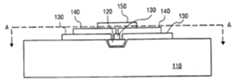
- FIG. 1illustrates a side view of an embodiment of a strap.
- FIG. 2illustrates a side view of an embodiment of the strap of FIG. 1 as attached to a large-scale component.
- FIG. 3Aillustrates a view of an embodiment of the apparatus of FIG. 1 along the line A-A in the direction indicated.
- FIG. 3Billustrates a view of an embodiment of the apparatus of FIG. 2 along the line B-B in the direction indicated.
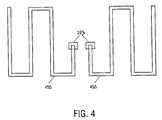
- FIG. 4illustrates an embodiment of an antenna.
- FIG. 5illustrates an embodiment of a web section having adhered thereon straps including functional blocks such as NanoBlock ®ICs (NanoBlock is a trademark and/or trade name of ALIEN technology Corporation).
- FIG. 6illustrates an embodiment of a method of forming an apparatus including both small-feature-size and large-feature-size components.
- FIG. 7illustrates an alternate embodiment of a method of forming an apparatus including both small-feature-size and large-feature-size components.
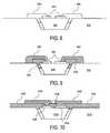
- FIG. 8illustrates an alternate embodiment of a strap from a side view.
- FIG. 9illustrates yet another alternate embodiment of a strap from a side view.
- FIG. 10illustrates a side view of still another alternate embodiment of a strap.
- FIG. 11illustrates another alternate embodiment of a method of forming an apparatus including both small-feature-size and large-feature-size components.
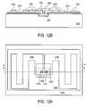
- FIG. 12Aillustrates a top view of another embodiment of a substrate.
- FIG. 12Billustrates a side view of another embodiment of a substrate.
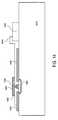
- FIG. 13illustrates a side view of yet another embodiment of a substrate.
- FIG. 14illustrates a side view of still another embodiment of a substrate.
- FIG. 15illustrates a side view of an embodiment of connecting conductors of a strap to conductors of a large-scale component.
- FIG. 16illustrates a side view of another embodiment of connecting conductors of a strap to conductors of a large-scale component.
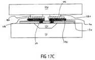
- FIGS. 17A-17Cillustrate side view of other embodiments of connecting conductors of a strap to conductors of a large-scale component.
- Embodiments of the present inventionrelate generally to the field of fabricating elements on a substrate.
- the inventionis an apparatus.
- the apparatusincludes a strap, comprising a substrate with an embedded integrated circuit (IC) embedded or contained therein.
- a first conductoris disposed on the substrate and attached to the IC.
- a conductive mediumis attached to the strap at the first conductor.
- the apparatusalso includes a large-scale component attached to the conductive medium, which allows the large-scale component to be electrically coupled to the integrated circuit.
- the large-scale componentmay include a second conductor that attaches to the conductive medium to electrically couple the large-scale component to the IC.
- the large-scale componentmay be included in another substrate.
- the substrate of the strap and the substrate carrying the large-scale componentmay be flipped over on top of one another to facilitate the coupling of the large-scale component to the IC.
- the IChas an active surface.
- the active surfacecan be the IC surface where the first conductor can be attached to the IC. In one embodiment, the active surface faces the large scale component.
- Some embodiments of the inventionrelate to a method of making an assembly.
- the methodincludes creating a strap by attaching a first conductor to a substrate that has an integrated circuit contained or embedded therein such that the first conductor is connected electrically to the integrated circuit.
- the methodalso includes attaching a large-scale component to the first conductor such that the large-scale component is electrically connected to the integrated circuit.
- a second conductoris included in the large-scale component. The second conductor connects electrically to the first conductor.
- a conductive mediumis used to connect the first conductor to the second conductor.
- the first conductor and/or the conductive mediumcan be formed.
- the materials used to form the first conductor and/or the conductive mediummay be applied by screen printing (e.g., flat bed screen printing or rotary screen printing), stencil printing, ink jet printing, gravure printing, flexography printing, pad stamping, electrostatic printing, laminating, hot pressing, laser assisted chemical vapor deposition, physical vapor deposition (e.g., sputtering), shadow masking, evaporating, extrusion coating, curtain coating, electroplating, or other additive techniques.
- the materialsmay also be applied by metering an appropriate amount of material (e.g., through a needle, nozzle, or pipette, or another convenient metering tool) onto a particular substrate or surface.
- the conductive mediummay be a fluid, ink (silver ink, of a thermoplastic or thermoset resin base), electrically conductive tape (thermoplastic or thermosetting polymer with conductive fillers), electrically conductive paste (solder paste or conductive fillers in a polymer matrix), solder, metal film, metal particles suspended in a carrier, conductive polymer, carbon-based conductor, or other thick-film material for example.
- a conductive medium productis Acheson Colloids 479SS.
- the inventionis an apparatus.
- the apparatusincludes an integrated circuit embedded within a substrate.
- the apparatusalso includes a dielectric layer formed over a portion of the integrated circuit and a portion of the substrate.
- the apparatusfurther includes a first conductor formed over a portion of the dielectric layer, the first conductor having direct electrical connection with the integrated circuit.
- the apparatusis called a strap.
- the inventionis a method.
- the methodincludes forming a dielectric on a portion of an integrated circuit and a portion of a substrate, the integrated circuit embedded within the substrate.
- the methodalso includes attaching a first conductor to the dielectric and to the integrated circuit, the first conductor electrically connected to the integrated circuit.
- the inventionis an apparatus.
- the apparatusincludes a substrate having embedded or contained therein an integrated circuit.
- a first conductoris attached to the substrate and the integrated circuit is attached to the first conductor.
- This apparatusis referred to as a strap.
- the apparatusalso includes a conductive medium attached to the first conductor of the integrated circuit.
- the inventionis an apparatus.
- the apparatusincludes a strap having embedded therein a functional block such as a NanoBlock IC.
- a functional blockis a small structure or a microstructure that includes an integrated circuit that can drive a particular device and a first conductor electrically coupled to the NanoBlock IC.
- the NanoBlock ICmay have been produced using conventional VLSI procedures and embedded using fluidic self-assembly (FSA), for example.
- FSAfluidic self-assembly
- the NanoBlock ICmay also be attached or contained in the substrate by other transferring methods.
- the substratehas attached thereon a conductive medium, allowing for electrical coupling between the NanoBlock IC and the first conductor.
- NanoBlock ICAs the IC that is being incorporated, contained, embedded, or included in the substrate, it is to be expected that other functional blocks can be used instead.
- the inventionis a method.
- the methodincludes attaching a first conductor to a substrate having embedded therein a NanoBlock IC such that the first conductor is coupled electrically to the NanoBlock IC, thereby forming a strap.
- the methodfurther includes attaching a large-scale component to the first conductor such that the large-scale component is electrically connected or coupled to the first conductor.
- the methodmay also include a conductive medium disposed between the first conductor and the large-scale component to interconnect the NanoBlock IC to the large-scale component.
- the methodmay further include fabricating the NanoBlock IC and performing FSA to embed the NanoBlock IC into the substrate, in one embodiment.
- the methodmay also involve a large-scale component which may be an antenna, a power source such as a battery or a button cell, or a thick-film cell printed on the strap or other substrate; a display electrode or a display; a logic device, or a sensor; among other examples.
- a large-scale componentwhich may be an antenna, a power source such as a battery or a button cell, or a thick-film cell printed on the strap or other substrate; a display electrode or a display; a logic device, or a sensor; among other examples.
- the inventionis an apparatus.
- the apparatusincludes a substrate having embedded or contained therein a NanoBlock IC.
- the substratehas attached thereto a first conductor, which allows for electrical connection between the NanoBlock IC and a conductive medium.
- the conductive mediumis attached to another a substrate such as an antenna. The conductive medium allows for electrical coupling between the antenna and the NanoBlock IC.
- the embodimentsmay involve a strap having a NanoBlock IC deposited therein.
- other functional blocks or other IC devicesmay be used instead without affecting the scope of the embodiments.
- the NanoBlock IC or other IC devicesmay be embedded within the strap or otherwise contained, included, or incorporated in the strap.
- FIG. 1illustrates a side view of an embodiment of a strap, including a substrate with an embedded functional block IC such as a NanoBlock IC, planarizing layer, and first conductor that contacts the NanoBlockTM IC.
- the NanoBlock ICincludes at least one conducting pad as is known in the art.
- the first conductorcontacts the NanoBlock IC by contacting the conducting pad.
- the substrate 110has an opening in it to contain a functional block or the NanoBlock IC 120 , and may be a flexible plastic substrate for example.
- the IC 120is a NanoBlock IC formed via conventional VLSI.
- the NanoBlock IC 120may be embedded or deposited in the opening of the substrate 110 through FSA in one embodiment, or by other transferring methods in other embodiments.
- the IC 120can also be transferred to the substrate 110 by other methods such as pick-and-place.
- the ICcan also be contained in the substrate 110 using other methods such as using a tool that can press the IC 120 into the substrate 110 or attaching the IC 120 to the substrate 110 by other convenient methods.
- the NanoBlock IC 120may have a variety of functions or structures consistent with an integrated circuit.
- the NanoBlock IC 120includes circuitry suitable for receiving radio signals from an external antenna and sending radio signals via the external antenna.
- the NanoBlock IC 120also has an active surface such as the surface that has the circuitry of the NanoBlock IC 120 .
- the NanoBlock IC 120may receive power from an external source via an external antenna, and use such power to send a radio signal via the external antenna. It is to be appreciated that even though the discussion focuses on the NanoBlock IC 120 , other IC can be used instead and that the embodiments are not limited to the NanoBlock 120 .
- a planarization layer 130Formed above the NanoBlock IC 120 is a planarization layer 130 , which may be formed through a conventional lamination or coating of an organic dielectric, pattern and etch or other similar method, for example.
- a planarization layer 130Formed above the planarization layer 130 are two first conductors 140 , which may be formed from a screen-printed electrically conductive paste for example, and which occupy two contact holes in the planarization layer 130 .
- the two first conductors 140attach to the conductive pads of NanoBlock IC 120 , and the two first conductors 140 preferably do not directly connect to each other.
- the first conductors 140are formed from a thermosetting ink that contains conductive fillers (e.g., conductive metals such as silver or polymers that are intrinsically conducting polymers (ICP), such as polyaniline) dispersed in a thermosetting polymer.
- first conductors 140are formed from a thermoplastic ink that contains similar conductive fillers as the thermosetting ink dispersed in a thermoplastic polymer.
- conductive fillersare not needed such as when the thermosetting material or the thermoplastic material is inherently conductive.
- the conductive thermosetting ink used to form the first conductors 140may be a one-part starting material, a two-part starting material or a multiple-part polymerizable starting material. After the thermosetting ink is deposited, it can be cured by exposure to reactive species such as oxygen, to heat, to moisture, or by exposure to an electromagnetic radiation such as IR, visible, UV, electron beams, RF, and microwave frequency.
- the conductive thermoplastic ink used to form the first conductors 140can be deposited as a softened polymer (by applying heat) and allowed to solidify.
- the first conductors 140may be formed with the conductive thermoplastic ink and solidified to form the first conductor 140 .
- the first conductors 140are being bonded to other conductors (such as conductors of a large-scale component). These embodiments allow for a direct electrical connection between the first conductors 140 and other conductors.
- the conductive thermoplastic inkmay be softened with an appropriate solvent in order to transfer/deposit the conductive thermoplastic ink in its softened form and then allow the softened thermoplastic ink to solidify to form the first conductors 140 .
- thermoplastic inkmay eliminate the need for an intermediate conductive medium 270 to electrically connect the first conductors 140 to other conductors (e.g., conductors 280 of a large-scale component below) since the thermoplastic material can be directly bonded to another conductor as it solidifies. These embodiments allow a direct electrical connection between the first conductors 140 and the other conductors.
- the first conductors 140can also be formed by other conductive materials such as silver, aluminum, or copper.
- the first conductors 140can be deposited by various techniques known in the art such as physical vapor deposition (e.g., sputtering), chemical vapor deposition or low-pressure vapor deposition, screen printing (e.g., flat bed screen printing or rotary screen printing), stencil printing, ink jet printing, gravure printing, flexography printing, electrostatic printing, laminating, hot pressing, laser assisted chemical vapor deposition, shadow masking, evaporating, extrusion coating, curtain coating, electroplating, or other additive techniques.
- physical vapor depositione.g., sputtering
- chemical vapor deposition or low-pressure vapor depositione.g., screen printing (e.g., flat bed screen printing or rotary screen printing), stencil printing, ink jet printing, gravure printing, flexography printing, electrostatic printing, laminating, hot pressing, laser assisted chemical vapor deposition, shadow masking,
- the first conductor 140is made from a conductive paste (such as those available from Acheson, including 479SS) and can be formed or deposited on the substrate 110 through a screen printing process, for example.
- the first conductors 140can be formed by pad transferring where preformed conductive pads are picked up by a robotic tool and transferred to the substrate 110 to form the first conductors 140 .
- the conductive padsare typically transferred in their softened state and allowed to be cured or solidified after being transferred onto the substrate 110 .
- an insulating layer 150is formed above the first conductors 140 .
- This insulating layer 150may be formed through a thin-film or thick-film process for example, and may fill in space between the two first conductors 140 .
- the first conductor 140may in some instances connect to multiple pads of an integrated circuit by design. One example of such a situation is connecting all ground pads of an IC to a single conductor to achieve a common ground potential.
- thin filmsare applied through use of vacuum or low-pressure processes. Thick films are applied using non-vacuum processes, typically at or near atmospheric pressure.
- non-vacuum processestypically at or near atmospheric pressure.
- the NanoBlock IC 120are formed with sufficiently large pads as to allow for direct connection between the first conductors 140 and other conductors (e.g., second conductors 280 of a large-scale component 281 , FIG. 2) and the NanoBlock IC, thereby avoiding the requirement of an intermediate or intervening conductor.
- direct (vertical) connection between any large-scale component and the NanoBlock ICis made through conductors that have isotropic conductivity.
- FIG. 2illustrates a side view of an embodiment of the strap of FIG. 1 as attached to a large-scale component 281 .
- the large-scale component discussed in this applicationmay be an antenna, an electronic display or display electrode, a sensor, a power source such as a battery or solar cell, or another logic or memory device (such as but not limited to microprocessors, memory, and other logic devices), for example.
- the first conductors 140are electrically coupled to other conductors provided on the large-scale components and in one embodiment, electrically coupled to second conductors 280 .
- the first conductors 140are electrically coupled to the second conductors 280 through a conductive medium 270 .
- the conductive medium 270includes two conductors 270 or alternatively, at least two conductors 270 .
- the conductors 270each have a direct connection to one of the first conductors 140 , and potentially having a contact to one or more of the insulating layer 150 , the planarization layer 130 , and the substrate 110 .
- Attached to each of the conductive media 270are one of the second conductors 280 , which may be conductive pads of an antenna or conductive ends of an antenna for example.
- the second conductormay be a conductor of other devices such as an electronic device, display electrode, sensor, power source, and logic/memory device.
- each of the second conductors 280may be said to be coupled (electrically) to the NanoBlock IC 120 .
- the conductive medium 270acts as an intermediate conductor for the first conductors 140 and the second conductors 280 .
- a substrate 290is the material in which the conductors 280 are embedded or to which the conductors 280 are attached, and is preferably insulating in nature. The substrate 290 and the second conductors 280 thus constitute the large-scale component 281 in one embodiment.
- a space 260is a space between the two conductors 270 , which may be occupied by the substrate 290 and/or the insulator 150 , may be left as a void in the structure, or may be filled by the conductive medium 270 if anisotropic in nature, for example. It is important to note that in most applications, each of the two conductive media 270 would not be connected directly to the other conductive media 270 , and a similar statement may be made with respect to the two second conductors 280 .
- areas that need not be conductivecan be deactivated using appropriate chemicals or using conventional patterning techniques (e.g., etching). For instance, a layer of an isotropic material can be blanket-deposited over the first conductors 140 to form a conductive layer for the conductive medium 270 . The isotropic material deposited over the area that need not be conductive, such as the space 260 , can be deactivated leaving the conductive area referred to as the conductive medium 270 .
- the conductive medium 270is an electrically conductive tape (such as those available from the 3M Corporation, including 3M Z-Axis 7303, for example).
- the conductive tapemay be isotropically or anisotropically conductive.
- Such a conductive tapemay be applied (adhered) by rolling the tape along a row of straps, applying sufficient pressure and possibly heat to adhere the tape to the straps, and then cutting the through the tape and the strap to separate the individual straps. This may be done in various manners.
- the conductive medium 270may be made from a conductive paste (such as those available from Acheson, including 479SS), which is deposited through a screen printing process, for example.
- the conductive pasteis screen printed on to the straps (e.g., on the substrate 110 portion of the strap and on at least portions of the first conductor 140 ) at moderate resolutions relative to overall manufacturing tolerances, thereby allowing for useful connection of the conductive medium 270 to the first conductors 140 .
- the conductive medium 270may also be made using metal particles suspended in a polymer carrier such as a thermoplastic material or a thermosetting material, a conductive polymer, a carbon-based conductor, a solder, or other conductive medium as will be appreciated by those skilled in the art.
- a polymer carriersuch as a thermoplastic material or a thermosetting material, a conductive polymer, a carbon-based conductor, a solder, or other conductive medium as will be appreciated by those skilled in the art.
- the conductive medium 270is a polymerized film having conductive particles suspended therein.
- the conductive particlescan be metals or conductive fibers (e.g., carbon).
- the conductive particlescan have a nonconductive core of various shapes, such as spheres or long continuous fibers that are coated with a conductive material.
- the conductive particlescan be carbon nanotubes.
- the polymerized filmcan be a thermosetting material or a thermoplastic material.
- the conductive medium 270is made of particles suspended in a carrier, conductive polymers, pastes, silver inks, carbon-base conductors, solders, and other suitable conductive materials.
- the conductive medium 270is a pressure sensitive adhesive (PSA) with conductive fillers (e.g., silver flake or particle, metals, fibers coated with conductive materials, or glass beads coated with conductive materials). Having the conductive medium 270 being a PSA with the conductive fillers provides a soft conformal layer between two rigid layers (e.g., the first conductor 140 and another conductor (e.g., the second conductors 280 ) to facilitate better contact.
- PSApressure sensitive adhesive
- One advantage of using a PSA film having the conductive fibersis that only a small amount of pressure (e.g., less than 25 psig) is needed to cause the connection between the first conductors 140 and the conductive medium 270 and or between the conductive medium 270 and the second conductors 280 .
- the conductive medium 270is replaced with a non-conductive adhesive 271 as shown in FIG. 15.
- heat and pressureare used to “rupture” a portion of the non-conductive adhesive 271 as shown in FIG. 15 so that the second conductors 280 and the first conductors 140 are brought into immediate contact with each other.
- portions of the non-conductive adhesive 271are locally pressed and heated so that they are thinned out or ruptured to allow the second conductors 280 to contact the first conductors 140 .
- the non-conductive adhesive 271functions to hold together substrate 290 (a substrate of a large-scale component 281 ) and substrate 110 while being ruptured at the portions that are dedicated for contact between the second conductors 280 and the first conductors 140 .
- the non-conductive adhesive 271functions to hold together portions of the first conductors 140 and the conductor second 280 as shown in FIG. 15 and are capacitively coupled.
- crimping or pressingcan be used to selectively press down on the substrate 290 to cause rupture in the non-conductive adhesive 271 at the crimped or pressed portions.
- the second conductors 280get pressed into the ruptured part and are pressed in contact with the first conductors 140 as shown in FIG. 15.
- the non-conductive adhesive 271is a thin layer of adhesive that can be ruptured when selectively crimped or pressed.
- the first conductors 140are formed on the substrate 110 as previously described.
- the non-conductive adhesive 271is disposed between the second conductors 280 and the first conductors 140 as an intervening layer.
- the non-conductive adhesive 271can be a hot melt or pressure sensitive adhesive film, for example.
- the assemblyis then mechanically crimped together, with or without heat and pressure, in such a fashion to cause the second conductors 280 to bend and pierce or penetrate through the non-conductive adhesive 271 creating an intimate connection between the first conductors 140 and the second conductors 280 .
- the non-conductive adhesive 271is used to form an edge-seal for the second conductors 280 and the first conductors 140 as shown in FIG. 16.
- the edge-sealwill keep the second conductors 280 and the first conductors 140 in intimate contact and as such, an intermediate conductor (e.g., the conductive medium 270 ) is not necessary.
- a thin layer of adhesiveis first deposited between the second conductors 280 and the first conductors 140 .
- a mechanical technique that will press the substrate 290 close to the substrate 110is then used to press down on the assembly.
- the non-conductive adhesive 271is pressed to the sides or edges of the first conductors 140 and second conductors 280 .
- the non-conductive adhesive 271is selectively pressed or compressed to cause it to migrate or flow to the edges of the first conductors 140 and second conductors 280 to allow the first conductors 140 and second conductors 280 to electrically connect as shown in FIG. 10.
- the non-conductive adhesive 271can be a hot-melt adhesive, a pressure sensitive adhesive, an electromagnetic radiation curable adhesive, (e.g., UV, IR, visible, RF, or microwave curable adhesive), a heat curable adhesive, a thermosetting material, a thermoplastic material, or a material that can flow out under pressure and/or heat to form an edge-seal upon solidifying.
- the non-conductive adhesive 271can be deposited either directly on the second conductors 280 and/or the first conductors 140 in its uncured or softened state and allowed to cure or solidify after the substrate 110 and the substrate 290 are pressed together. As the non-conductive adhesive 271 solidifies, it forms edge-seals around the first conductors 140 and second conductors 280 to keep these two conductors in immediate contact with each other for the electrical connection.
- small and sharp particles 291 as shown in FIG. 17A-17Ccan be incorporated to enhance the physical interconnection and/or the electrical interconnection between the first conductors 140 and the second conductors 280 , either directly or through the use of the intermediate layer (e.g., the conductive medium 270 or the non-conductive adhesive 271 ).
- the particles 291are especially advantageous when the first conductors 140 and the second conductors 280 may contain a small residue of either contaminates or oxide that may hinder the connection.
- the small and sharp particlese.g., fine diamond, glass, or any other hard, small particles that have irregular shapes
- the conductive ink/paste or the non-conductive adhesivecan then be screen-printed or stencil printed or dispensed as previously described.
- the particleswill penetrate through the surface and abrade the contamination and thus improve the contact or connection made to the first conductors 140 and the second conductors 280 .
- the small and sharp particles 291can act as mechanical interlocks to enhance the connection as shown in FIGS. 17A-17C.
- the small and sharp particles (e.g., diamonds) 291are dispensed in the conductive pastes or inks that are used to form the first conductors 140 or the second conductors 280 .
- the first conductors 140 and second conductors 280are to be directly connected to each other without the use of an intermediate layer.
- the small and sharp particles (e.g., diamonds) 291are dispensed in a thermosetting ink having conductive fillers that is used to form the first conductors 140 or the second conductors 280 .
- the small and sharp particles (e.g., diamonds) 291are dispensed in a thermoplastic ink having conductive fillers that is used to form the first conductors 140 or the second conductors 280 .
- the particles 291 for the thermoplastic inkmay be slightly larger in size to compensate for the softening of the ink.
- the thermosetting ink having the particles 291 or the thermoplastic ink having the particles 291is then allowed to solidify using methods previously mentioned or other convenient methods to form the first conductors 140 or the second conductors 280 . After the first conductors 140 or the second conductors 280 are solidified, the small and sharp particles 291 reside at the surfaces of the first conductors 140 or the second conductors 280 .
- particles 291then act as mechanical interlock to help maintaining the contact between the first conductors 140 and the second conductors 280 .
- the particles 291are coated with a conductive material to further enhance or ensure the electrical interconnection between the first conductors 140 and the second conductors 280 .
- the sharp and small particles 291are incorporated into a non-conductive adhesive 271 and the substrate 110 and the substrate 290 are pressed together such that the non-conductive adhesive 271 are pushed to the outer edges of the first conductors 140 and the second conductors 280 as shown in FIG. 17B.
- the first conductors 140 and second conductors 280are directly connected to each other without the use of an intermediate layer.
- the non-conductive adhesive 271can be a thin layer of adhesive and can first be deposited between the second conductors 280 and the first conductors 140 .
- a mechanical technique that will press the substrate 290 close to the substrate 110is then used to press down on the assembly.
- the non-conductive adhesive 271is pressed to the sides or edges of the first conductors 140 and second conductors 280 .
- the non-conductive adhesive 271is selectively pressed or compressed to cause it to migrate/flow to the edges of the first conductors 140 and second conductors 280 to allow the first conductors 140 and second conductors 280 to electrically connect.
- the non-conductive adhesive 271can be a hot-melt adhesive, a pressure sensitive adhesive, an electromagnetic radiation curable adhesive, (e.g., UV, IR, visible, RF, or microwave curable adhesive), a thermosetting material, or a thermoplastic material.
- the non-conductive adhesive 271can be deposited either directly on the second conductors 280 and/or the first conductors 140 in its uncured or softened state and allowed to solidify after the substrate 110 and the substrate 290 are pressed together. As the nonconductive adhesive 271 solidifies, it forms edge-seals around the first conductors 140 and second conductors 280 to keep these two conductors in immediate contact with each other for the electrical connection.
- the small particles 291function as the mechanical interlock that further maintains that attachment between the first conductors 140 and the second conductors 280 .
- the particles 291are incorporated into a conductive medium 270 .
- the particles 291will reside at the surfaces of the conductive medium 270 , as shown in FIG. 17C.
- the particles 291provide an added mechanical interlocking feature for the conductive medium 270 .
- the conductive medium 270can be a polymerized film having conductive particles suspended therein such as a thermosetting ink having conductive fillers or a thermoplastic having conductive fillers.
- the conductive medium 271acts as an intermediate conductor for the first conductors 140 and the second conductors 280 .
- the particles (e.g., diamonds) 291 dispensed in the conductive medium 270provide an extra mechanical interlock for the conductive medium 270 to the first conductors 140 and/or second conductors 280 .
- the particles 291can also be coated with a conductive material to increase conductivity.
- the first conductors 140 and second conductors 280are directly connected to each other.
- solderingis used to directly attach the first conductors 140 to the conductors 280 .
- Conventional soldering technique or laser solderingcan be used to solder the first conductors 140 to the second conductors 280 .
- Conventional solder joiningtypically uses a low melting point metallic alloy to join two metallic surfaces (e.g., the first conductors 140 and second conductors 280 ).
- solderis heated up to its melting point and placed between the two metallic surfaces to be joined while still in its molten state. It is usually important that both metallic surfaces be specially prepared to promote adhesion with the solder. Thus, both the first conductors 140 and second conductors 280 need to be prepared to promote adhesion with the solder.
- a small bit of solderin paste form, for example
- a laseris used to heat up the solder to bond the first conductors 140 and the second conductors 280 together.
- Laser solderingoffers the use of a solder as a strap attach method even though plastic substrates (e.g., the substrate 110 and/or 290 ) are involved in the process.
- the lasercan heat up the solder so fast and with such positional accuracy that the plastic substrates can potentially survive the operation.
- laser weldingis used to directly attach the first conductors 140 to the second conductors 280 .
- a high energy IR laseris used to provide a precisely positioned heat source to fuse two compatible metals together. It is envisioned that the high speed, high precision of a laser can be used in the attachment process to melt/fuse the first conductors 140 and the second conductors 280 together to form a strong conductive bond.
- One way this might be accomplishedis to appropriately position the substrate 110 over the substrate 290 and use the laser to heat the attachment area (e.g., the area where the first conductors 140 and second conductors 280 need to contact or connect) to a temperature high enough to fuse the surfaces of the two first conductors 140 and second conductors 280 together. It is conceivable that the heat required might actually burn a hole through the supporting plastic materials. This is acceptable as long as a mechanical/electrical bond is formed for the first conductors 140 and second conductors 280 .
- the first conductors 140 and the second conductors 280are typically made of conductive materials that are compatible to one another.
- holesmay be created through the substrate 290 or 110 as the first conductors 140 and second conductors 280 are being soldered or welded together. This is acceptable as these holes are not significantly large so as to affect the function of the assembly.
- crimpingis used to cause the first conductors 140 to electrically couple to the second conductors 280 .
- a crimping toole.g., pliers, die and plate
- pliers, die and platecan be used to compress the first conductors 140 to the second conductors 280 .
- the first conductors 140can be coupled to the second conductors 280 directly and without the addition of any conductive medium/adhesive or non-conductive adhesives as previous discussed. These embodiments can use mechanical bonding techniques to create the connection for the first conductors 140 and second conductors 280 .
- a metallic rivet, rod, staple, or wirecan be used to punch through the first conductors 140 and the second conductors 280 to establish the mechanical attachment to allow for the electrical interconnection between the first conductors 140 and the second conductors 280 .
- a rivet gun, pressurized air gun, hammer, robotic actuator, stapler, air gun, mechanical impulse device, or other convenient toolis used to accomplish the mechanical attachment.
- the first conductors 140are placed in temporary contact with the second conductors 280 and then crimped together to create a long-lived electrical connection.
- the crimpingcould be accomplished in a variety of ways.
- the first conductors 140 and second conductors 280could be compressed between the teeth of a pair of pliers, a crimp die and a flat plate, or a crimp die and a complementary plate.
- the crimp diecould have a variety of component features on it designed to drive a portion of either the first conductors 140 on one component feature, and the second conductors 280 on the other component feature.
- An impulse below, such as from a hammer, air piston, or mechanical actuatorcould also be used to facilitate the crimping.
- a pin-shaped die with a corresponding plates on the opposite sideis used to mechanically bond the first conductors 140 and 280 together. Pushing the die into the plate causes the conductor in the topmost plate to deform into the conductor on the bottom plate. When this deformation is sufficiently large, a portion of the top conductor will stay partially deformed within the bottom conductor, such that electrical contact is established.
- Electrical connection of the first conductors 140 and the second conductors 280could also be connected together using a wire (not shown) that is sewn into the first conductors 140 and second conductors 280 .
- the wirecould be pulled through the conductors or stitched into the conductors with a purely manual system, such as sewing, or a more automated system, such as conductive filament attachment.
- the sewn connectioncould be one stitch or a number of stitches, depending on the required strength of the connection.
- the substrate 110can simply be taped to the substrate 290 that could be a substrate of a large-scale component using conventional taping technique to tightly hold the two substrates together such that the first conductors 140 and the second conductors 280 are in contact with each other to allow for the electrical connection.
- the substrate 110 supporting the first conductors 140is laid over the substrate 240 supporting the second conductors 280 . Then an adhesive tape is applied over the substrate 110 and onto the substrate 290 , such that the substrate 110 is held against the substrate 290 with the first conductors 140 and second conductors 280 in intimate contact with each other.
- the adhesive tapecould be a pressure sensitive adhesive film, a dry film with a B-staged thermoset adhesive, a UV-curing adhesive, to name a few possibilities.
- the adhesive tapecould be applied to the substrate 110 on the substrate 290 , or, alternatively, the substrate 110 could be placed on the adhesive tape to begin with, and then the adhesive tape could be applied to the substrate 290 such that the first conductors 140 on the substrate 110 is appropriately aligned with respect to the second conductors 280 on the substrate 290 .
- first conductors 140 and the second conductors 280can be electrically connected through various mechanical methods.
- thermosonic bondingis used to bond the first conductors 140 and the conductors 280 together. Thermosonic bonding is useful when the first conductors 140 and the second conductors 280 are made of materials that easily fuse together.
- either the substrate 110 or the substrate 290will need to be heated. This can be done by placing the substrate to be heated on a heated stage. If necessary, the substrate ( 110 or 290 ) can be heated by heating the pick-up tool. Other methods of heating the substrate may be used, such as heated gas.
- the substrate 110is then placed on the substrate 290 such that the first conductors 140 touch the second conductors 280 . Pressure is then applied to the assembly to ensure good contact. Ultrasonic energy (vibration) is next applied to the assembly for a predetermine length of time.
- a polymer layermay be introduced between the bonding head of the bonding tool and the substrate 110 or substrate 290 .
- Thermosonic bondingrequires less time than some of the other methods.
- Thermosonic bondingcan be used to fuse metals (e.g., Au—Au) and thus can offer lower contact resistance.
- the addition of ultrasonic energyallows for interface temperature to be lower than otherwise may be required.
- thermocompression bondingis used to bond the first conductors 140 and the second conductors 280 together.
- Thermocompression bondingis also useful when the first conductors 140 and the second conductors 280 are made of materials that do not easily fuse together.
- Thermocompression bondingis similar to thermosonic bonding except that instead of having the ultrasonic energy, thermocompression uses pressure to get the physical contact.
- thermosonic bonding and thermocompression bondingcan be used to bond the first conductors 140 and the second conductors 280 together when an intermediate medium (e.g., conductive medium 270 or non-conductive adhesive 271 ) is deposited between the first conductors 140 and the second conductors 280 as previously described.
- an intermediate mediume.g., conductive medium 270 or non-conductive adhesive 271
- FIG. 3Aillustrates a view of an embodiment of the strap of FIG. 1 along the line A-A in the direction indicated.
- the various overlaps between the substrate 110 , the NanoBlock IC 120 , the planarization layer 130 , the first conductors 140 and the insulating layer 150are all illustrated.
- contact holes 315 in the planarization layer 130are illustrated, thus making apparent the connection between the first conductors 140 and the NanoBlock IC 120 .
- FIG. 3Billustrates a view of an embodiment of the apparatus of FIG. 2 along the line B-B in the direction indicated. Illustrated are overlaps between the first conductors 140 , the insulating layer 150 , and the second conductors 280 . For clarity, the substrate 110 is also shown and the substrate 290 is not shown.
- FIG. 4illustrates an embodiment of an antenna.
- Each arm 455is connected to antenna conductor pad 283 , which is the same as the second conductor 280 in one embodiment.
- the arms 455may simply form the antenna conductor that includes the antenna conductor pads 283 , making them a single unitary structure of both arm and pad.
- FIG. 5illustrates an embodiment of a web section having adhered thereon straps including NanoBlock ICs.
- Each strap 505(of which one exemplary strap 505 is labeled) is adhered to a pair of electrically conductive tape strips 515 .
- the tape strips 515form part of a larger spool, which also includes through-holes 525 for purposes of spooling.
- the tape strips 515may be anisotropically conductive film (ACF), with the conductors (e.g., the first conductors 140 ) of the straps 505 adhered to the ACF.
- the tape spoolsmay be formed with gaps between columns of straps 515 allowing for slitting the tape through the gap to produce a single column of straps.
- ACFanisotropically conductive film
- FIG. 6illustrates an embodiment of a method of forming an apparatus including both small-feature-size and large-feature-size components.
- the integrated circuitsare fabricated, such as through a conventional VLSI method.
- the integrated circuitsare embedded into substrate(s).
- processing for purposes of forming planarization and insulation layersoccurs, and an insulator is formed (one skilled in the art will appreciate that a thin-film or a thick-film insulation layer may also be formed).
- a conductive mediumis applied to the substrate, such as by screen printing on paste or through other additive processes.
- a large-scale componentis attached to the conductive medium.
- the tape spool of FIG. 5may be used to attach a large volume of straps to large-scale components by attaching each strap individually and then cutting the tape after attachment.
- the conductive medium 640is applied directly to the substrate that contains ICs 620 , omitting the insulating layer.
- FIG. 7illustrates an alternative embodiment of a method of forming an apparatus including both small-feature-size and large-feature-size components, with particular reference to fabrication of RF-ID tags using functional blocks such as NanoBlock ICs.
- NanoBlock ICsare fabricated, such as through conventional VLSI methods. It is to be appreciated that the NanoBlock IC can be deposited, attached, or otherwise contained in the substrate by other suitable methods.
- NanoBlock ICsare embedded in substrates through FSA.
- any necessary post-FSA processing for purposes of forming planarization layers, and/or insulation layers,occurs. In particular, at least one thin-film dielectric is formed.
- the thin-film dielectricmay not be necessary in alternative embodiments.
- a first conductive mediumis applied to the substrates, such as in the form of a paste screened on to the substrates for example, thus creating straps.
- an electrically conductive tapeis adhered to the conductive medium on the straps.
- antennasare attached to the straps, such that the antennas are electrically coupled to the NanoBlock ICs of the corresponding straps.
- FIG. 8illustrates an alternate embodiment of a strap from a side view.
- the embodiment of FIG. 8is similar to the embodiment of FIG. 1.
- FIG. 8illustrates a substrate 810 , having embedded or contained therein (in an opening) an integrated circuit 820 , with pads 825 .
- Each of the pads 825has deposited thereon through use of an additive process a first conductor 840 , such as a silver ink for example.
- the first conductor 840is deposited such that it contacts one and only one pad 825 directly, thus allowing for separate conductors for each electrical contact of a circuit.
- the size of the pads 825may be greater than the size of similar pads on an integrated circuit such as the NanoBlock IC 120 of FIG. 1, in that the pads 825 must interface directly with material (the first conductor 840 ) having a much larger feature size than is common for VLSI devices.
- the first conductor 840may be expected to have an as-deposited thickness of approximately 10-15 ⁇ ms and a final thickness on the order of 1 ⁇ m or less, and that pads 825 may have minimum dimensions on the order of 20 ⁇ 20 ⁇ ms or more.
- FIG. 9illustrates yet another alternate embodiment of a strap from a side view.
- FIG. 9illustrates a similar embodiment to that of FIG. 8, which further incorporates an insulator.
- a substrate 910 including an integrated circuit 920 embedded or contained thereinis provided.
- Pads 925are a part of the integrated circuit 920 , and may be expected to have similar dimensions to the pads 825 .
- An insulating layer (dielectric) 930is deposited on the integrated circuit 920 through use of a thick film process. The insulating layer 930 may be expected to have a thickness on the order of 10 microns.
- first conductor 940which covers both the insulating layer 930 and some portion of a pad 925 , thus, allowing for electrical contact between the integrated circuit 920 and a large-scale component (e.g., through a second conductor included with the large-scale component).
- the first conductor 940may be expected to have similar characteristics to the first conductor 840 .
- FIG. 10illustrates a side view of still another alternate embodiment of a strap.
- a substrate 1010 including an integrated circuit 1020 incorporated or contained thereinis provided.
- an insulator 1030is formed on top of the substrate 1010 .
- the insulator 1030is a patterned with vias through which the first conductors 1040 may achieve contact with the conductive pads 1025 of the integrated circuit 1020 .
- the viasrequire greater precision in patterning than do any of the insulators of conductor components of FIGS. 8 and 9.
- the substrate 1010may have the insulator 1030 covering nearly its whole surface, rather than the limited areas of FIG. 9.
- the pads 1025may be smaller on the integrated circuit 1020 than similar pads of the integrated circuits 920 and 820 .
- FIG. 11illustrates another alternate embodiment of a method of forming an apparatus including both small-feature-size and large-feature-size components.
- an integrated circuitis embedded within a supporting substrate.
- an insulatoris applied to the substrate.
- the insulatoris patterned such as through a photolithographic thin-film process, whereby portions of the insulator are removed to expose portions of the substrate or integrated circuit, such as bond or conductive pads. Further cleaning, such as washing away photoresist for example, may be involved as part of application, patterning, or even in a post-etch phase.
- a photosensitive insulator or dielectricmay be used, thereby eliminating the need for photoresist for example.
- a conductive materialis applied to the substrate, coating all or part of the insulator to form first conductors.
- the conductive materialis processed (such as by heat curing, for example) as necessary to form a proper conductor (e.g., the first conductors).
- a proper conductore.g., the first conductors.
- curing of silver inkis known in the art to be possible at 90-100° C. for some formulations with a reasonable cure time for various manufacturing processes. It will be appreciated that cure times do vary, and that those skilled in the art may adapt cure processes to the needs of a surrounding manufacturing process and the devices to be produced.
- the large-scale componentis attached to the first conductor, thereby achieving electrical coupling with the integrated circuit.
- the large-scale componentincludes second conductors wherein the first conductors and the second conductors (either directly or through a conductive medium as previously discussed) electrically interconnect the IC to the large-scale component. Also note that the final processing of the first conductor of block 1160 may be performed after the large-scale component is attached at block 1170 .
- a large-feature-size componentmay be incorporated as part of the strap, such as an embedded conductor acting as an antenna, or may be formed on the strap as illustrated in FIGS. 12A and 12B. Printing or otherwise using additive processing technology to form an antenna 1240 of the conductive medium on the strap is one option.
- NanoBlock ICor other small or micro functional blocks with such large-feature-size components on the strap may be accomplished through use of a conductors 1440 , allowing for electrical coupling between a large-feature-size components 1460 and a small-feature-size (NanoBlock IC for example) components 1420 , as in FIG. 14.
- a conductive medium 1340may be used to interconnect two or more small-feature-size components embedded in a single substrate, such as two NanoBlock ICs for example, as illustrated in FIG. 13.
- FIG. 12Aillustrates a top view of another embodiment of a substrate.
- a substrate 1210may be a substrate such as those discussed previously, including a flexible or rigid material.
- An IC 1220is embedded in an opening in the substrate 1210 .
- An insulator 1230is a layer of insulating material (or a dielectric layer) formed on top of both the substrate 1210 and the IC 1220 and may have planarizing properties.
- Contact holes 1215are holes in the insulator 1230 above contact pads of the IC 1220 , allowing for physical contact and electrical connection between the IC 1220 and a first conductor 1240 .
- An insulating layer 1250is another insulator or dielectric above portions of the first conductor 1240 , the insulator 1220 and the substrate 1210 , and above all of the IC 1220 .
- first conductor 1240is formed into two arms of an antenna, such as may be useful for radio frequency applications.
- batteries, sensors, power supplies, button cells, and displays and display electrodesmay also be formed through use of conductors and/or conductive media and other materials.
- FIG. 12Billustrates a side view of another embodiment of a substrate.
- the first conductor 1240occupies contact holes 1215 of FIG. 12A to contact directly with the IC 1220 .
- the segments illustrated with respect to the first conductor 1240correspond to the various segments of the antenna as it traces its path along the surface of the insulator 1230 .
- the presence of the insulator 1230may not be necessary in some instances.
- FIG. 13illustrates a side view of yet another embodiment of a substrate.
- a substrate 1310includes a first IC 1320 and a second IC 1325 .
- An insulator 1330is formed above the IC 1320 , the IC 1325 and the substrate 1310 .
- a first conductor 1340is formed the above insulator 1330 , and contacts both the IC 1320 and the IC 1325 .
- One portion of the first conductor 1340forms an electrical connection between the IC 1320 and the IC 1325 , thereby electrically coupling the IC 1320 to the IC 1325 .
- Above both of the IC 1320 and IC 1325are formed insulator layers 1350 .
- FIG. 14illustrates a side view of still another embodiment of a substrate.
- a substrate 1410has embedded or contained in an opening therein an IC 1420 .
- Formed above the substrate 1410 and the IC 1420is an insulator 1430 .
- Formed above the insulator 1430 and, connected to the IC 1420is a conductor 1440 , a portion of which is connected to a sensor 1460 , thereby electrically coupling the IC 1420 to the sensor 1460 .
- insulator 1450Formed above a portion of the conductor 1440 and the insulator 1430 is an insulator 1450 , which may or may not be of the same material as the insulator 1430 .
Landscapes
- Engineering & Computer Science (AREA)
- Microelectronics & Electronic Packaging (AREA)
- Computer Hardware Design (AREA)
- Power Engineering (AREA)
- Physics & Mathematics (AREA)
- General Physics & Mathematics (AREA)
- Condensed Matter Physics & Semiconductors (AREA)
- Theoretical Computer Science (AREA)
- Manufacturing & Machinery (AREA)
- Combinations Of Printed Boards (AREA)
- Wire Bonding (AREA)
Abstract
Description
- This is a continuation in part of U.S. patent application Ser. No. 10/056,192, filed on Jan. 23, 2002 entitled “Apparatus incorporating small-feature-size and large-feature-size components and method for making same” which has the Attorney Docket No. 003424.P056. The mentioned Application is hereby incorporated by reference in its entirety.[0001]
- 1. Field of the Invention[0002]
- The field of the invention generally relates to apparatuses having both large-feature-size components and small-feature-size components, and methods of making such apparatuses. The invention more particularly relates to combination of VLSI integrated circuits and macro-scale components to form a single device.[0003]
- 2. Description of the Related Art[0004]
- VLSI provides many effective methods for creation of microscopic-scale and smaller components. Such miniaturization provides many advantages in terms of speed of operation, size of footprint, amount of necessary resources, and speed of manufacture for electronic devices.[0005]
- Unfortunately, some components of electronic devices are not well-suited to formation through well-known VLSI processes. These components often are necessarily very large (macroscopic-scale) relative to devices or components of devices formed through VLSI. One such component is an antenna, which may need to have a characteristic length to allow for adequate transmission on a preferred frequency, and for which the characteristic length in question may be appropriately measured in centimeters or meters, for example. Formation of a conductor for use as an antenna using VLSI tends to waste time and material resources, as a 30 cm conductor (for example) can easily be formed through less expensive processes.[0006]
- Thus, the problem then becomes a matter of combining a large-scale component such as an antenna with a small-scale component such as an integrated circuit. For a conventional radio, this may involve use of packaging for the integrated circuit, conductors on a printed circuit board, a connector attached to the printed circuit board, and an antenna attached to the connector. This approach is simple enough for a device having rigid packaging and flexible size constraints. However, other applications may have more demanding requirements for size and materials cost.[0007]
- In particular, it may be useful to have a small radio-transmitter with flexible materials allowing for bending and other abusive actions without degradation in functionality. Similarly, such a small radio-transmitter may need to be producible rapidly in quantities of millions or billions, thus requiring ease of assembly and relatively inexpensive materials on a per-unit basis. Using a printed-circuit board approach for such a radio-transmitter will likely not succeed. Moreover, avoiding such time (and/or space) consuming processing operations as thermal cure may be advantageous.[0008]
- It is possible to separately produce elements, such as integrated circuits and then place them where desired on a different and perhaps larger substrate. Prior techniques can be generally divided into two types: deterministic methods or random methods. Deterministic methods, such as pick and place, use a human or robot arm to pick each element and place it into its corresponding location in a different substrate. Pick and place methods place devices generally one at a time, and are generally not applicable to very small or numerous elements such as those needed for large arrays, such as an active matrix liquid crystal display. Random placement techniques are more effective and result in high yields if the elements to be placed have the right shape. U.S. Pat. No. 5,545,291 and U.S. Pat. No. 5,904,545 describe methods that use random placement. In this method, microstructures are assembled onto a different substrate through fluid transport. This is sometimes referred to as fluidic self assembly (FSA). Using this technique, various integrated circuits, each containing a functional component, may be fabricated on one substrate and then separated from that substrate and assembled onto a separate substrate through the fluidic self assembly process. The process involves combining the integrated circuits with a fluid, and dispensing the fluid and integrated circuits over the surface of a receiving substrate that has receptor regions or openings. The integrated circuits flow in the fluid over the surface and randomly align into receptor regions, thereby becoming embedded in the substrate.[0009]
- Once the integrated circuits have been deposited into the receptor regions, the remainder of the device can be assembled. Typically, this involves coating the substrate with a planarization layer to provide electrical insulation and physical retention for the integrated circuits. The planarization layer creates a level surface on top of the substrate by filling in the portions of the receptor regions that are not filled by integrated circuits. After the planarization layer has been deposited, other elements, including pixel electrodes and traces for example, may be installed.[0010]
- Using FSA, the functional components of the device can be manufactured and tested separately from the rest of the device.[0011]
- The embodiments of the present invention relates generally to the field of fabricating elements on a substrate. One embodiment pertains to an apparatus that includes a substrate having embedded, contained, or incorporated therein an integrated circuit. The integrated circuit is attached to a first conductor disposed on the substrate. The first conductor can be a thermosetting or a thermoplastic material. The apparatus also includes a large-scale component attached to the first conductor; the large-scale component is thus electrically coupled to the integrated circuit. The large-scale component includes a second substrate.[0012]
- Another embodiment pertains to a method that includes attaching a conductive medium to a substrate having embedded or contained therein an integrated circuit such that the conductive medium is connected electrically to the integrated circuit. The method further includes a conductive medium attached to the first conductor of the integrated circuit. The method also includes attaching a large-scale component to the conductive medium such that the large-scale component is electrically connected to the integrated circuit.[0013]
- In other embodiments, various methods and materials used to attach the large-scale component to the first conductor are described. In some embodiments, anisotropically conductive materials are used to attach the conductor from the large-scale component to the first conductor on the substrate that has an integrated circuit (IC) contained or embedded therein so that there is electrical and physical connection between the large-scale component and the IC. In other embodiments, isotropically conductive materials are used to attach the conductor from the large-scale component to the first conductor on the substrate that has the IC contained or embedded therein so that there is an electrical and physical connection between the IC and the large-scale component. In some embodiments, the conductor on the substrate that has the IC contained or embedded therein and the conductor of the large-scale component are connected using mechanical methods to keep the conductors in intimate contact. Such mechanical methods include crimping, clinching, pressing, ultrasonic energy, heat and pressure, taping, compressing, stapling, punching, riveting, thermosonic bonding, and thermo-compression bonding methods. These mechanical methods bring the conductors into an immediate contact to allow for the necessary electrical interconnection between the large-scale component and the IC.[0014]
- The present invention is illustrated by way of example and not limitation in the accompanying figures.[0015]
- FIG. 1 illustrates a side view of an embodiment of a strap.[0016]
- FIG. 2 illustrates a side view of an embodiment of the strap of FIG. 1 as attached to a large-scale component.[0017]
- FIG. 3A illustrates a view of an embodiment of the apparatus of FIG. 1 along the line A-A in the direction indicated.[0018]
- FIG. 3B illustrates a view of an embodiment of the apparatus of FIG. 2 along the line B-B in the direction indicated.[0019]
- FIG. 4 illustrates an embodiment of an antenna.[0020]
- FIG. 5 illustrates an embodiment of a web section having adhered thereon straps including functional blocks such as NanoBlock ®ICs (NanoBlock is a trademark and/or trade name of ALIEN technology Corporation).[0021]
- FIG. 6 illustrates an embodiment of a method of forming an apparatus including both small-feature-size and large-feature-size components.[0022]
- FIG. 7 illustrates an alternate embodiment of a method of forming an apparatus including both small-feature-size and large-feature-size components.[0023]
- FIG. 8 illustrates an alternate embodiment of a strap from a side view.[0024]
- FIG. 9 illustrates yet another alternate embodiment of a strap from a side view.[0025]
- FIG. 10 illustrates a side view of still another alternate embodiment of a strap.[0026]
- FIG. 11 illustrates another alternate embodiment of a method of forming an apparatus including both small-feature-size and large-feature-size components.[0027]
- FIG. 12A illustrates a top view of another embodiment of a substrate.[0028]
- FIG. 12B illustrates a side view of another embodiment of a substrate.[0029]
- FIG. 13 illustrates a side view of yet another embodiment of a substrate.[0030]
- FIG. 14 illustrates a side view of still another embodiment of a substrate.[0031]
- FIG. 15 illustrates a side view of an embodiment of connecting conductors of a strap to conductors of a large-scale component.[0032]
- FIG. 16 illustrates a side view of another embodiment of connecting conductors of a strap to conductors of a large-scale component.[0033]
- FIGS. 17A-17C illustrate side view of other embodiments of connecting conductors of a strap to conductors of a large-scale component.[0034]
- An apparatus incorporating small-feature-size and large-feature-size components and method for making same is described. In the following description, for purposes of explanation, numerous specific details are set forth in order to provide a thorough understanding of the invention. It will be apparent to one skilled in the art, however, that the invention can be practiced without these specific details. In other instances, structures and devices are shown in block diagram form to avoid obscuring the invention.[0035]
- Reference in the specification to “one embodiment” or “an embodiment” means that a particular feature, structure, or characteristic described in connection with the embodiment is included in at least one embodiment of the invention. The appearances of the phrase “in one embodiment” in various places in the specification are not necessarily all referring to the same embodiment, nor are separate or alternative embodiments mutually exclusive of other embodiments.[0036]
- Embodiments of the present invention relate generally to the field of fabricating elements on a substrate. In one embodiment, the invention is an apparatus. The apparatus includes a strap, comprising a substrate with an embedded integrated circuit (IC) embedded or contained therein. A first conductor is disposed on the substrate and attached to the IC. A conductive medium is attached to the strap at the first conductor. The apparatus also includes a large-scale component attached to the conductive medium, which allows the large-scale component to be electrically coupled to the integrated circuit. The large-scale component may include a second conductor that attaches to the conductive medium to electrically couple the large-scale component to the IC. The large-scale component may be included in another substrate. The substrate of the strap and the substrate carrying the large-scale component may be flipped over on top of one another to facilitate the coupling of the large-scale component to the IC. In one embodiment, the IC has an active surface. The active surface can be the IC surface where the first conductor can be attached to the IC. In one embodiment, the active surface faces the large scale component.[0037]
- Some embodiments of the invention relate to a method of making an assembly. The method includes creating a strap by attaching a first conductor to a substrate that has an integrated circuit contained or embedded therein such that the first conductor is connected electrically to the integrated circuit. The method also includes attaching a large-scale component to the first conductor such that the large-scale component is electrically connected to the integrated circuit. In some embodiments, a second conductor is included in the large-scale component. The second conductor connects electrically to the first conductor. In some embodiments, a conductive medium is used to connect the first conductor to the second conductor.[0038]
- There are many ways that the first conductor and/or the conductive medium can be formed. The materials used to form the first conductor and/or the conductive medium may be applied by screen printing (e.g., flat bed screen printing or rotary screen printing), stencil printing, ink jet printing, gravure printing, flexography printing, pad stamping, electrostatic printing, laminating, hot pressing, laser assisted chemical vapor deposition, physical vapor deposition (e.g., sputtering), shadow masking, evaporating, extrusion coating, curtain coating, electroplating, or other additive techniques. The materials may also be applied by metering an appropriate amount of material (e.g., through a needle, nozzle, or pipette, or another convenient metering tool) onto a particular substrate or surface.[0039]
- The conductive medium may be a fluid, ink (silver ink, of a thermoplastic or thermoset resin base), electrically conductive tape (thermoplastic or thermosetting polymer with conductive fillers), electrically conductive paste (solder paste or conductive fillers in a polymer matrix), solder, metal film, metal particles suspended in a carrier, conductive polymer, carbon-based conductor, or other thick-film material for example. One exemplary conductive medium product is Acheson Colloids 479SS.[0040]
- In another alternate embodiment, the invention is an apparatus. The apparatus includes an integrated circuit embedded within a substrate. The apparatus also includes a dielectric layer formed over a portion of the integrated circuit and a portion of the substrate. The apparatus further includes a first conductor formed over a portion of the dielectric layer, the first conductor having direct electrical connection with the integrated circuit. The apparatus is called a strap.[0041]
- In yet another alternate embodiment, the invention is a method. The method includes forming a dielectric on a portion of an integrated circuit and a portion of a substrate, the integrated circuit embedded within the substrate. The method also includes attaching a first conductor to the dielectric and to the integrated circuit, the first conductor electrically connected to the integrated circuit.[0042]
- In still another alternate embodiment, the invention is an apparatus. The apparatus includes a substrate having embedded or contained therein an integrated circuit. A first conductor is attached to the substrate and the integrated circuit is attached to the first conductor. This apparatus is referred to as a strap. The apparatus also includes a conductive medium attached to the first conductor of the integrated circuit.[0043]
- In yet another alternate embodiment, the invention is an apparatus. The apparatus includes a strap having embedded therein a functional block such as a NanoBlock IC. A functional block is a small structure or a microstructure that includes an integrated circuit that can drive a particular device and a first conductor electrically coupled to the NanoBlock IC. The NanoBlock IC may have been produced using conventional VLSI procedures and embedded using fluidic self-assembly (FSA), for example. The NanoBlock IC may also be attached or contained in the substrate by other transferring methods. The substrate has attached thereon a conductive medium, allowing for electrical coupling between the NanoBlock IC and the first conductor. The conductive medium is electrically connected to the first conductor. Attached to the conductive medium is a substrate including an antenna, allowing for electrical coupling between the antenna and the NanoBlock IC.[0044]
- Although the discussion herein focuses on the NanoBlock IC as the IC that is being incorporated, contained, embedded, or included in the substrate, it is to be expected that other functional blocks can be used instead.[0045]
- In still another alternate embodiment, the invention is a method. The method includes attaching a first conductor to a substrate having embedded therein a NanoBlock IC such that the first conductor is coupled electrically to the NanoBlock IC, thereby forming a strap. The method further includes attaching a large-scale component to the first conductor such that the large-scale component is electrically connected or coupled to the first conductor. The method may also include a conductive medium disposed between the first conductor and the large-scale component to interconnect the NanoBlock IC to the large-scale component. The method may further include fabricating the NanoBlock IC and performing FSA to embed the NanoBlock IC into the substrate, in one embodiment. The method may also involve a large-scale component which may be an antenna, a power source such as a battery or a button cell, or a thick-film cell printed on the strap or other substrate; a display electrode or a display; a logic device, or a sensor; among other examples.[0046]
- In a further alternate embodiment, the invention is an apparatus. The apparatus includes a substrate having embedded or contained therein a NanoBlock IC. The substrate has attached thereto a first conductor, which allows for electrical connection between the NanoBlock IC and a conductive medium. The conductive medium is attached to another a substrate such as an antenna. The conductive medium allows for electrical coupling between the antenna and the NanoBlock IC.[0047]
- For purposes of the discussion in this document, the embodiments may involve a strap having a NanoBlock IC deposited therein. However, other functional blocks or other IC devices may be used instead without affecting the scope of the embodiments. In addition, the NanoBlock IC or other IC devices may be embedded within the strap or otherwise contained, included, or incorporated in the strap.[0048]
- FIG. 1 illustrates a side view of an embodiment of a strap, including a substrate with an embedded functional block IC such as a NanoBlock IC, planarizing layer, and first conductor that contacts the NanoBlock™ IC. The NanoBlock IC includes at least one conducting pad as is known in the art. The first conductor contacts the NanoBlock IC by contacting the conducting pad. The[0049]
substrate 110 has an opening in it to contain a functional block or theNanoBlock IC 120, and may be a flexible plastic substrate for example. In one embodiment, theIC 120 is a NanoBlock IC formed via conventional VLSI. TheNanoBlock IC 120 may be embedded or deposited in the opening of thesubstrate 110 through FSA in one embodiment, or by other transferring methods in other embodiments. TheIC 120 can also be transferred to thesubstrate 110 by other methods such as pick-and-place. The IC can also be contained in thesubstrate 110 using other methods such as using a tool that can press theIC 120 into thesubstrate 110 or attaching theIC 120 to thesubstrate 110 by other convenient methods. - The[0050]
NanoBlock IC 120 may have a variety of functions or structures consistent with an integrated circuit. In one embodiment, theNanoBlock IC 120 includes circuitry suitable for receiving radio signals from an external antenna and sending radio signals via the external antenna. TheNanoBlock IC 120 also has an active surface such as the surface that has the circuitry of theNanoBlock IC 120. Moreover, in one embodiment, theNanoBlock IC 120 may receive power from an external source via an external antenna, and use such power to send a radio signal via the external antenna. It is to be appreciated that even though the discussion focuses on theNanoBlock IC 120, other IC can be used instead and that the embodiments are not limited to theNanoBlock 120. - Formed above the[0051]
NanoBlock IC 120 is aplanarization layer 130, which may be formed through a conventional lamination or coating of an organic dielectric, pattern and etch or other similar method, for example. Formed above theplanarization layer 130 are twofirst conductors 140, which may be formed from a screen-printed electrically conductive paste for example, and which occupy two contact holes in theplanarization layer 130. In one embodiment, the twofirst conductors 140 attach to the conductive pads ofNanoBlock IC 120, and the twofirst conductors 140 preferably do not directly connect to each other. - In one embodiment, the[0052]
first conductors 140 are formed from a thermosetting ink that contains conductive fillers (e.g., conductive metals such as silver or polymers that are intrinsically conducting polymers (ICP), such as polyaniline) dispersed in a thermosetting polymer. Alternatively,first conductors 140 are formed from a thermoplastic ink that contains similar conductive fillers as the thermosetting ink dispersed in a thermoplastic polymer. In some embodiments, conductive fillers are not needed such as when the thermosetting material or the thermoplastic material is inherently conductive. - The conductive thermosetting ink used to form the[0053]
first conductors 140 may be a one-part starting material, a two-part starting material or a multiple-part polymerizable starting material. After the thermosetting ink is deposited, it can be cured by exposure to reactive species such as oxygen, to heat, to moisture, or by exposure to an electromagnetic radiation such as IR, visible, UV, electron beams, RF, and microwave frequency. - The conductive thermoplastic ink used to form the[0054]
first conductors 140 can be deposited as a softened polymer (by applying heat) and allowed to solidify. In some embodiments, thefirst conductors 140 may be formed with the conductive thermoplastic ink and solidified to form thefirst conductor 140. Thefirst conductors 140 are being bonded to other conductors (such as conductors of a large-scale component). These embodiments allow for a direct electrical connection between thefirst conductors 140 and other conductors. In other embodiments, the conductive thermoplastic ink may be softened with an appropriate solvent in order to transfer/deposit the conductive thermoplastic ink in its softened form and then allow the softened thermoplastic ink to solidify to form thefirst conductors 140. Using the conductive thermoplastic ink may eliminate the need for an intermediate conductive medium270 to electrically connect thefirst conductors 140 to other conductors (e.g.,conductors 280 of a large-scale component below) since the thermoplastic material can be directly bonded to another conductor as it solidifies. These embodiments allow a direct electrical connection between thefirst conductors 140 and the other conductors. - The[0055]
first conductors 140 can also be formed by other conductive materials such as silver, aluminum, or copper. Thefirst conductors 140 can be deposited by various techniques known in the art such as physical vapor deposition (e.g., sputtering), chemical vapor deposition or low-pressure vapor deposition, screen printing (e.g., flat bed screen printing or rotary screen printing), stencil printing, ink jet printing, gravure printing, flexography printing, electrostatic printing, laminating, hot pressing, laser assisted chemical vapor deposition, shadow masking, evaporating, extrusion coating, curtain coating, electroplating, or other additive techniques. In one embodiment, thefirst conductor 140 is made from a conductive paste (such as those available from Acheson, including 479SS) and can be formed or deposited on thesubstrate 110 through a screen printing process, for example. In another embodiment, thefirst conductors 140 can be formed by pad transferring where preformed conductive pads are picked up by a robotic tool and transferred to thesubstrate 110 to form thefirst conductors 140. The conductive pads are typically transferred in their softened state and allowed to be cured or solidified after being transferred onto thesubstrate 110. - In one embodiment, an insulating[0056]
layer 150 is formed above thefirst conductors 140. This insulatinglayer 150 may be formed through a thin-film or thick-film process for example, and may fill in space between the twofirst conductors 140. As will be appreciated, thefirst conductor 140 may in some instances connect to multiple pads of an integrated circuit by design. One example of such a situation is connecting all ground pads of an IC to a single conductor to achieve a common ground potential. - In some embodiments, thin films are applied through use of vacuum or low-pressure processes. Thick films are applied using non-vacuum processes, typically at or near atmospheric pressure. One having skill in the art will appreciate that exact magnitudes of ambient pressure for low-pressure of vacuum as opposed to atmospheric pressure may be difficult to state. However, one having skill in the art will also appreciate that the differences between low-pressure and atmospheric pressure are relatively large compared to atmospheric pressure.[0057]
- In some embodiments, the[0058]
NanoBlock IC 120 are formed with sufficiently large pads as to allow for direct connection between thefirst conductors 140 and other conductors (e.g.,second conductors 280 of a large-scale component 281, FIG. 2) and the NanoBlock IC, thereby avoiding the requirement of an intermediate or intervening conductor. In other embodiments, direct (vertical) connection between any large-scale component and the NanoBlock IC is made through conductors that have isotropic conductivity. - FIG. 2 illustrates a side view of an embodiment of the strap of FIG. 1 as attached to a large-[0059]
scale component 281. The large-scale component discussed in this application may be an antenna, an electronic display or display electrode, a sensor, a power source such as a battery or solar cell, or another logic or memory device (such as but not limited to microprocessors, memory, and other logic devices), for example. - In attaching the strap to the large-[0060]
scale component 281, thefirst conductors 140 are electrically coupled to other conductors provided on the large-scale components and in one embodiment, electrically coupled tosecond conductors 280. In one embodiment, thefirst conductors 140 are electrically coupled to thesecond conductors 280 through aconductive medium 270. In one embodiment, theconductive medium 270 includes twoconductors 270 or alternatively, at least twoconductors 270. - In one embodiment, the[0061]
conductors 270 each have a direct connection to one of thefirst conductors 140, and potentially having a contact to one or more of the insulatinglayer 150, theplanarization layer 130, and thesubstrate 110. Attached to each of theconductive media 270 are one of thesecond conductors 280, which may be conductive pads of an antenna or conductive ends of an antenna for example. Alternatively, the second conductor may be a conductor of other devices such as an electronic device, display electrode, sensor, power source, and logic/memory device. In one embodiment, there are two or alternatively, at least twosecond conductors 280. Thus, as illustrated, each of thesecond conductors 280 may be said to be coupled (electrically) to theNanoBlock IC 120. The conductive medium270 acts as an intermediate conductor for thefirst conductors 140 and thesecond conductors 280. In one embodiment, asubstrate 290 is the material in which theconductors 280 are embedded or to which theconductors 280 are attached, and is preferably insulating in nature. Thesubstrate 290 and thesecond conductors 280 thus constitute the large-scale component 281 in one embodiment. - A[0062]
space 260 is a space between the twoconductors 270, which may be occupied by thesubstrate 290 and/or theinsulator 150, may be left as a void in the structure, or may be filled by theconductive medium 270 if anisotropic in nature, for example. It is important to note that in most applications, each of the twoconductive media 270 would not be connected directly to the otherconductive media 270, and a similar statement may be made with respect to the twosecond conductors 280. - In embodiments where the[0063]
conductive medium 270 is isotropic, areas that need not be conductive can be deactivated using appropriate chemicals or using conventional patterning techniques (e.g., etching). For instance, a layer of an isotropic material can be blanket-deposited over thefirst conductors 140 to form a conductive layer for theconductive medium 270. The isotropic material deposited over the area that need not be conductive, such as thespace 260, can be deactivated leaving the conductive area referred to as theconductive medium 270. - In one embodiment, the[0064]
conductive medium 270 is an electrically conductive tape (such as those available from the 3M Corporation, including 3M Z-Axis 7303, for example). Moreover, the conductive tape may be isotropically or anisotropically conductive. Such a conductive tape may be applied (adhered) by rolling the tape along a row of straps, applying sufficient pressure and possibly heat to adhere the tape to the straps, and then cutting the through the tape and the strap to separate the individual straps. This may be done in various manners. - Alternatively, the[0065]
conductive medium 270 may be made from a conductive paste (such as those available from Acheson, including 479SS), which is deposited through a screen printing process, for example. In one embodiment, the conductive paste is screen printed on to the straps (e.g., on thesubstrate 110 portion of the strap and on at least portions of the first conductor140) at moderate resolutions relative to overall manufacturing tolerances, thereby allowing for useful connection of theconductive medium 270 to thefirst conductors 140. Furthermore, theconductive medium 270 may also be made using metal particles suspended in a polymer carrier such as a thermoplastic material or a thermosetting material, a conductive polymer, a carbon-based conductor, a solder, or other conductive medium as will be appreciated by those skilled in the art. - In an alternative embodiment, the[0066]
conductive medium 270 is a polymerized film having conductive particles suspended therein. The conductive particles can be metals or conductive fibers (e.g., carbon). Alternatively, the conductive particles can have a nonconductive core of various shapes, such as spheres or long continuous fibers that are coated with a conductive material. Alternatively, the conductive particles can be carbon nanotubes. In addition, the polymerized film can be a thermosetting material or a thermoplastic material. - In some embodiment, the[0067]
conductive medium 270 is made of particles suspended in a carrier, conductive polymers, pastes, silver inks, carbon-base conductors, solders, and other suitable conductive materials. - In another embodiment, the[0068]
conductive medium 270 is a pressure sensitive adhesive (PSA) with conductive fillers (e.g., silver flake or particle, metals, fibers coated with conductive materials, or glass beads coated with conductive materials). Having theconductive medium 270 being a PSA with the conductive fillers provides a soft conformal layer between two rigid layers (e.g., thefirst conductor 140 and another conductor (e.g., the second conductors280) to facilitate better contact. One advantage of using a PSA film having the conductive fibers is that only a small amount of pressure (e.g., less than 25 psig) is needed to cause the connection between thefirst conductors 140 and theconductive medium 270 and or between theconductive medium 270 and thesecond conductors 280. - In another embodiment, instead of using the[0069]
conductive medium 270 as the intermediate conductor to connect thefirst conductors 140 and thesecond conductor 280, theconductive medium 270 is replaced with anon-conductive adhesive 271 as shown in FIG. 15. In this embodiment, heat and pressure are used to “rupture” a portion of thenon-conductive adhesive 271 as shown in FIG. 15 so that thesecond conductors 280 and thefirst conductors 140 are brought into immediate contact with each other. Thus, portions of thenon-conductive adhesive 271 are locally pressed and heated so that they are thinned out or ruptured to allow thesecond conductors 280 to contact thefirst conductors 140. In one embodiment, the non-conductive adhesive271 functions to hold together substrate290 (a substrate of a large-scale component281) andsubstrate 110 while being ruptured at the portions that are dedicated for contact between thesecond conductors 280 and thefirst conductors 140. In another embodiment, the non-conductive adhesive271 functions to hold together portions of thefirst conductors 140 and the conductor second280 as shown in FIG. 15 and are capacitively coupled. In one embodiment, crimping or pressing can be used to selectively press down on thesubstrate 290 to cause rupture in thenon-conductive adhesive 271 at the crimped or pressed portions. Thesecond conductors 280 get pressed into the ruptured part and are pressed in contact with thefirst conductors 140 as shown in FIG. 15. In one embodiment, thenon-conductive adhesive 271 is a thin layer of adhesive that can be ruptured when selectively crimped or pressed. - In one embodiment, the[0070]
first conductors 140 are formed on thesubstrate 110 as previously described. Thenon-conductive adhesive 271 is disposed between thesecond conductors 280 and thefirst conductors 140 as an intervening layer. Thenon-conductive adhesive 271 can be a hot melt or pressure sensitive adhesive film, for example. The assembly is then mechanically crimped together, with or without heat and pressure, in such a fashion to cause thesecond conductors 280 to bend and pierce or penetrate through thenon-conductive adhesive 271 creating an intimate connection between thefirst conductors 140 and thesecond conductors 280. - In another embodiment, the[0071]
non-conductive adhesive 271 is used to form an edge-seal for thesecond conductors 280 and thefirst conductors 140 as shown in FIG. 16. The edge-seal will keep thesecond conductors 280 and thefirst conductors 140 in intimate contact and as such, an intermediate conductor (e.g., the conductive medium270) is not necessary. In this embodiment, a thin layer of adhesive is first deposited between thesecond conductors 280 and thefirst conductors 140. A mechanical technique that will press thesubstrate 290 close to thesubstrate 110 is then used to press down on the assembly. As thesubstrate 290 and thesubstrate 110 are pressed together, thenon-conductive adhesive 271 is pressed to the sides or edges of thefirst conductors 140 andsecond conductors 280. In one embodiment, where thefirst conductors 140 andsecond conductors 280 contact, thenon-conductive adhesive 271 is selectively pressed or compressed to cause it to migrate or flow to the edges of thefirst conductors 140 andsecond conductors 280 to allow thefirst conductors 140 andsecond conductors 280 to electrically connect as shown in FIG. 10. - The[0072]
non-conductive adhesive 271 can be a hot-melt adhesive, a pressure sensitive adhesive, an electromagnetic radiation curable adhesive, (e.g., UV, IR, visible, RF, or microwave curable adhesive), a heat curable adhesive, a thermosetting material, a thermoplastic material, or a material that can flow out under pressure and/or heat to form an edge-seal upon solidifying. Thenon-conductive adhesive 271 can be deposited either directly on thesecond conductors 280 and/or thefirst conductors 140 in its uncured or softened state and allowed to cure or solidify after thesubstrate 110 and thesubstrate 290 are pressed together. As thenon-conductive adhesive 271 solidifies, it forms edge-seals around thefirst conductors 140 andsecond conductors 280 to keep these two conductors in immediate contact with each other for the electrical connection. - In any of the embodiments previously discussed, small and[0073]
sharp particles 291 as shown in FIG. 17A-17C can be incorporated to enhance the physical interconnection and/or the electrical interconnection between thefirst conductors 140 and thesecond conductors 280, either directly or through the use of the intermediate layer (e.g., theconductive medium 270 or the non-conductive adhesive271). Theparticles 291 are especially advantageous when thefirst conductors 140 and thesecond conductors 280 may contain a small residue of either contaminates or oxide that may hinder the connection. The small and sharp particles (e.g., fine diamond, glass, or any other hard, small particles that have irregular shapes) can be blended with the conductive ink or paste or the non-conductive adhesives. The conductive ink/paste or the non-conductive adhesive can then be screen-printed or stencil printed or dispensed as previously described. In one embodiment, during the bonding process of thefirst conductors 140 to thesecond conductors 280, the particles will penetrate through the surface and abrade the contamination and thus improve the contact or connection made to thefirst conductors 140 and thesecond conductors 280. In another embodiment, the small andsharp particles 291 can act as mechanical interlocks to enhance the connection as shown in FIGS. 17A-17C. - In one embodiment, as shown in FIG. 17A, the small and sharp particles (e.g., diamonds)[0074]291 are dispensed in the conductive pastes or inks that are used to form the
first conductors 140 or thesecond conductors 280. In this embodiment, thefirst conductors 140 andsecond conductors 280 are to be directly connected to each other without the use of an intermediate layer. In one embodiment, the small and sharp particles (e.g., diamonds)291 are dispensed in a thermosetting ink having conductive fillers that is used to form thefirst conductors 140 or thesecond conductors 280. In another embodiment, the small and sharp particles (e.g., diamonds)291 are dispensed in a thermoplastic ink having conductive fillers that is used to form thefirst conductors 140 or thesecond conductors 280. Theparticles 291 for the thermoplastic ink may be slightly larger in size to compensate for the softening of the ink. The thermosetting ink having theparticles 291 or the thermoplastic ink having theparticles 291 is then allowed to solidify using methods previously mentioned or other convenient methods to form thefirst conductors 140 or thesecond conductors 280. After thefirst conductors 140 or thesecond conductors 280 are solidified, the small andsharp particles 291 reside at the surfaces of thefirst conductors 140 or thesecond conductors 280. Theseparticles 291 then act as mechanical interlock to help maintaining the contact between thefirst conductors 140 and thesecond conductors 280. In an alternative embodiment, theparticles 291 are coated with a conductive material to further enhance or ensure the electrical interconnection between thefirst conductors 140 and thesecond conductors 280. - In another embodiment, the sharp and[0075]
small particles 291 are incorporated into anon-conductive adhesive 271 and thesubstrate 110 and thesubstrate 290 are pressed together such that thenon-conductive adhesive 271 are pushed to the outer edges of thefirst conductors 140 and thesecond conductors 280 as shown in FIG. 17B. In this embodiment, thefirst conductors 140 andsecond conductors 280 are directly connected to each other without the use of an intermediate layer. Thenon-conductive adhesive 271 can be a thin layer of adhesive and can first be deposited between thesecond conductors 280 and thefirst conductors 140. A mechanical technique that will press thesubstrate 290 close to thesubstrate 110 is then used to press down on the assembly. As thesubstrate 290 and thesubstrate 110 are pressed together, thenon-conductive adhesive 271 is pressed to the sides or edges of thefirst conductors 140 andsecond conductors 280. In one embodiment, where thefirst conductors 140 andsecond conductors 280 contact, thenon-conductive adhesive 271 is selectively pressed or compressed to cause it to migrate/flow to the edges of thefirst conductors 140 andsecond conductors 280 to allow thefirst conductors 140 andsecond conductors 280 to electrically connect. - The[0076]
non-conductive adhesive 271 can be a hot-melt adhesive, a pressure sensitive adhesive, an electromagnetic radiation curable adhesive, (e.g., UV, IR, visible, RF, or microwave curable adhesive), a thermosetting material, or a thermoplastic material. Thenon-conductive adhesive 271 can be deposited either directly on thesecond conductors 280 and/or thefirst conductors 140 in its uncured or softened state and allowed to solidify after thesubstrate 110 and thesubstrate 290 are pressed together. As thenonconductive adhesive 271 solidifies, it forms edge-seals around thefirst conductors 140 andsecond conductors 280 to keep these two conductors in immediate contact with each other for the electrical connection. In addition, thesmall particles 291 function as the mechanical interlock that further maintains that attachment between thefirst conductors 140 and thesecond conductors 280. - In one embodiment, the[0077]
particles 291 are incorporated into aconductive medium 270. Theparticles 291 will reside at the surfaces of theconductive medium 270, as shown in FIG. 17C. Theparticles 291 provide an added mechanical interlocking feature for theconductive medium 270. As previously described, theconductive medium 270 can be a polymerized film having conductive particles suspended therein such as a thermosetting ink having conductive fillers or a thermoplastic having conductive fillers. The conductive medium271 acts as an intermediate conductor for thefirst conductors 140 and thesecond conductors 280. In addition, the particles (e.g., diamonds)291 dispensed in theconductive medium 270 provide an extra mechanical interlock for theconductive medium 270 to thefirst conductors 140 and/orsecond conductors 280. Theparticles 291 can also be coated with a conductive material to increase conductivity. - In another embodiment, instead of using the[0078]
conductive medium 270,non-conductive adhesive 271, or sharp andsmall particles 291 to create and/or enhance the electrical and mechanical connection between thefirst conductors 140 and thesecond conductors 280, thefirst conductors 140 andsecond conductors 280 are directly connected to each other. In one embodiment, soldering is used to directly attach thefirst conductors 140 to theconductors 280. Conventional soldering technique or laser soldering can be used to solder thefirst conductors 140 to thesecond conductors 280. Conventional solder joining typically uses a low melting point metallic alloy to join two metallic surfaces (e.g., thefirst conductors 140 and second conductors280). The solder is heated up to its melting point and placed between the two metallic surfaces to be joined while still in its molten state. It is usually important that both metallic surfaces be specially prepared to promote adhesion with the solder. Thus, both thefirst conductors 140 andsecond conductors 280 need to be prepared to promote adhesion with the solder. In the laser soldering technique, a small bit of solder (in paste form, for example) can be placed between thefirst conductors 140 and thesecond conductors 280 and a laser is used to heat up the solder to bond thefirst conductors 140 and thesecond conductors 280 together. Laser soldering offers the use of a solder as a strap attach method even though plastic substrates (e.g., thesubstrate 110 and/or290) are involved in the process. The laser can heat up the solder so fast and with such positional accuracy that the plastic substrates can potentially survive the operation. - In an alternative embodiment, laser welding is used to directly attach the[0079]
first conductors 140 to thesecond conductors 280. Typically in laser welding, a high energy IR laser is used to provide a precisely positioned heat source to fuse two compatible metals together. It is envisioned that the high speed, high precision of a laser can be used in the attachment process to melt/fuse thefirst conductors 140 and thesecond conductors 280 together to form a strong conductive bond. One way this might be accomplished is to appropriately position thesubstrate 110 over thesubstrate 290 and use the laser to heat the attachment area (e.g., the area where thefirst conductors 140 andsecond conductors 280 need to contact or connect) to a temperature high enough to fuse the surfaces of the twofirst conductors 140 andsecond conductors 280 together. It is conceivable that the heat required might actually burn a hole through the supporting plastic materials. This is acceptable as long as a mechanical/electrical bond is formed for thefirst conductors 140 andsecond conductors 280. - When using the soldering or welding method, the[0080]
first conductors 140 and thesecond conductors 280 are typically made of conductive materials that are compatible to one another. In some embodiment, holes may be created through thesubstrate first conductors 140 andsecond conductors 280 are being soldered or welded together. This is acceptable as these holes are not significantly large so as to affect the function of the assembly. - In another embodiment, crimping is used to cause the[0081]
first conductors 140 to electrically couple to thesecond conductors 280. In this embodiment, a crimping tool (e.g., pliers, die and plate) can be used to compress thefirst conductors 140 to thesecond conductors 280. - In other embodiments, the[0082]
first conductors 140 can be coupled to thesecond conductors 280 directly and without the addition of any conductive medium/adhesive or non-conductive adhesives as previous discussed. These embodiments can use mechanical bonding techniques to create the connection for thefirst conductors 140 andsecond conductors 280. A metallic rivet, rod, staple, or wire can be used to punch through thefirst conductors 140 and thesecond conductors 280 to establish the mechanical attachment to allow for the electrical interconnection between thefirst conductors 140 and thesecond conductors 280. A rivet gun, pressurized air gun, hammer, robotic actuator, stapler, air gun, mechanical impulse device, or other convenient tool is used to accomplish the mechanical attachment. - In one embodiment, the[0083]
first conductors 140 are placed in temporary contact with thesecond conductors 280 and then crimped together to create a long-lived electrical connection. The crimping could be accomplished in a variety of ways. For example, thefirst conductors 140 andsecond conductors 280 could be compressed between the teeth of a pair of pliers, a crimp die and a flat plate, or a crimp die and a complementary plate. The crimp die could have a variety of component features on it designed to drive a portion of either thefirst conductors 140 on one component feature, and thesecond conductors 280 on the other component feature. An impulse below, such as from a hammer, air piston, or mechanical actuator could also be used to facilitate the crimping. - In another embodiment, a pin-shaped die with a corresponding plates on the opposite side is used to mechanically bond the[0084]
first conductors - Electrical connection of the[0085]
first conductors 140 and thesecond conductors 280 could also be connected together using a wire (not shown) that is sewn into thefirst conductors 140 andsecond conductors 280. The wire could be pulled through the conductors or stitched into the conductors with a purely manual system, such as sewing, or a more automated system, such as conductive filament attachment. The sewn connection could be one stitch or a number of stitches, depending on the required strength of the connection. - In one embodiment, the[0086]
substrate 110 can simply be taped to thesubstrate 290 that could be a substrate of a large-scale component using conventional taping technique to tightly hold the two substrates together such that thefirst conductors 140 and thesecond conductors 280 are in contact with each other to allow for the electrical connection. In one embodiment, thesubstrate 110 supporting thefirst conductors 140 is laid over the substrate240 supporting thesecond conductors 280. Then an adhesive tape is applied over thesubstrate 110 and onto thesubstrate 290, such that thesubstrate 110 is held against thesubstrate 290 with thefirst conductors 140 andsecond conductors 280 in intimate contact with each other. The adhesive tape could be a pressure sensitive adhesive film, a dry film with a B-staged thermoset adhesive, a UV-curing adhesive, to name a few possibilities. The adhesive tape could be applied to thesubstrate 110 on thesubstrate 290, or, alternatively, thesubstrate 110 could be placed on the adhesive tape to begin with, and then the adhesive tape could be applied to thesubstrate 290 such that thefirst conductors 140 on thesubstrate 110 is appropriately aligned with respect to thesecond conductors 280 on thesubstrate 290. - In another embodiment, the[0087]
first conductors 140 and thesecond conductors 280 can be electrically connected through various mechanical methods. In one embodiment, thermosonic bonding is used to bond thefirst conductors 140 and theconductors 280 together. Thermosonic bonding is useful when thefirst conductors 140 and thesecond conductors 280 are made of materials that easily fuse together. In one embodiment, either thesubstrate 110 or thesubstrate 290 will need to be heated. This can be done by placing the substrate to be heated on a heated stage. If necessary, the substrate (110 or290) can be heated by heating the pick-up tool. Other methods of heating the substrate may be used, such as heated gas. Thesubstrate 110 is then placed on thesubstrate 290 such that thefirst conductors 140 touch thesecond conductors 280. Pressure is then applied to the assembly to ensure good contact. Ultrasonic energy (vibration) is next applied to the assembly for a predetermine length of time. In one embodiment, to accommodate for any planarity angle between the bonding tool and the part a polymer layer may be introduced between the bonding head of the bonding tool and thesubstrate 110 orsubstrate 290. Thermosonic bonding requires less time than some of the other methods. Thermosonic bonding can be used to fuse metals (e.g., Au—Au) and thus can offer lower contact resistance. The addition of ultrasonic energy allows for interface temperature to be lower than otherwise may be required. - In one embodiment, thermocompression bonding is used to bond the[0088]
first conductors 140 and thesecond conductors 280 together. Thermocompression bonding is also useful when thefirst conductors 140 and thesecond conductors 280 are made of materials that do not easily fuse together. Thermocompression bonding is similar to thermosonic bonding except that instead of having the ultrasonic energy, thermocompression uses pressure to get the physical contact. - In addition, thermosonic bonding and thermocompression bonding can be used to bond the[0089]
first conductors 140 and thesecond conductors 280 together when an intermediate medium (e.g.,conductive medium 270 or non-conductive adhesive271) is deposited between thefirst conductors 140 and thesecond conductors 280 as previously described. - FIG. 3A illustrates a view of an embodiment of the strap of FIG. 1 along the line A-A in the direction indicated. The various overlaps between the[0090]
substrate 110, theNanoBlock IC 120, theplanarization layer 130, thefirst conductors 140 and the insulatinglayer 150 are all illustrated. Moreover, contact holes315 in theplanarization layer 130 are illustrated, thus making apparent the connection between thefirst conductors 140 and theNanoBlock IC 120. - FIG. 3B illustrates a view of an embodiment of the apparatus of FIG. 2 along the line B-B in the direction indicated. Illustrated are overlaps between the[0091]
first conductors 140, the insulatinglayer 150, and thesecond conductors 280. For clarity, thesubstrate 110 is also shown and thesubstrate 290 is not shown. - FIG. 4 illustrates an embodiment of an antenna. Each[0092]
arm 455 is connected toantenna conductor pad 283, which is the same as thesecond conductor 280 in one embodiment. Note that in an alternate embodiment, thearms 455 may simply form the antenna conductor that includes theantenna conductor pads 283, making them a single unitary structure of both arm and pad. - FIG. 5 illustrates an embodiment of a web section having adhered thereon straps including NanoBlock ICs. Each strap[0093]505 (of which one
exemplary strap 505 is labeled) is adhered to a pair of electrically conductive tape strips515. The tape strips515 form part of a larger spool, which also includes through-holes 525 for purposes of spooling. In one embodiment, the tape strips515 may be anisotropically conductive film (ACF), with the conductors (e.g., the first conductors140) of thestraps 505 adhered to the ACF. Moreover, the tape spools may be formed with gaps between columns ofstraps 515 allowing for slitting the tape through the gap to produce a single column of straps. - FIG. 6 illustrates an embodiment of a method of forming an apparatus including both small-feature-size and large-feature-size components. At[0094]
block 610, the integrated circuits are fabricated, such as through a conventional VLSI method. Atblock 620, the integrated circuits are embedded into substrate(s). Atblock 630, processing for purposes of forming planarization and insulation layers occurs, and an insulator is formed (one skilled in the art will appreciate that a thin-film or a thick-film insulation layer may also be formed). Atblock 640, a conductive medium is applied to the substrate, such as by screen printing on paste or through other additive processes. Atblock 650, a large-scale component is attached to the conductive medium. Note that in one embodiment, the tape spool of FIG. 5 may be used to attach a large volume of straps to large-scale components by attaching each strap individually and then cutting the tape after attachment. In an alternate embodiment, theconductive medium 640 is applied directly to the substrate that containsICs 620, omitting the insulating layer. - FIG. 7 illustrates an alternative embodiment of a method of forming an apparatus including both small-feature-size and large-feature-size components, with particular reference to fabrication of RF-ID tags using functional blocks such as NanoBlock ICs. At[0095]
block 710, NanoBlock ICs are fabricated, such as through conventional VLSI methods. It is to be appreciated that the NanoBlock IC can be deposited, attached, or otherwise contained in the substrate by other suitable methods. At block720, NanoBlock ICs are embedded in substrates through FSA. Atblock 730, any necessary post-FSA processing for purposes of forming planarization layers, and/or insulation layers, occurs. In particular, at least one thin-film dielectric is formed. As will be appreciated by one skilled in the art, the thin-film dielectric may not be necessary in alternative embodiments. Atblock 740, a first conductive medium is applied to the substrates, such as in the form of a paste screened on to the substrates for example, thus creating straps. Atblock 750, an electrically conductive tape is adhered to the conductive medium on the straps. Atblock 760, antennas are attached to the straps, such that the antennas are electrically coupled to the NanoBlock ICs of the corresponding straps. - FIG. 8 illustrates an alternate embodiment of a strap from a side view. As will be appreciated, the embodiment of FIG. 8 is similar to the embodiment of FIG. 1. However, FIG. 8 illustrates a[0096]
substrate 810, having embedded or contained therein (in an opening) anintegrated circuit 820, withpads 825. Each of thepads 825 has deposited thereon through use of an additive process afirst conductor 840, such as a silver ink for example. Usually, but not always, thefirst conductor 840 is deposited such that it contacts one and only onepad 825 directly, thus allowing for separate conductors for each electrical contact of a circuit. - Moreover, it will be appreciated that the size of the[0097]
pads 825 may be greater than the size of similar pads on an integrated circuit such as theNanoBlock IC 120 of FIG. 1, in that thepads 825 must interface directly with material (the first conductor840) having a much larger feature size than is common for VLSI devices. Note that in one embodiment, thefirst conductor 840 may be expected to have an as-deposited thickness of approximately 10-15 μms and a final thickness on the order of 1 μm or less, and thatpads 825 may have minimum dimensions on the order of 20×20 μms or more. - FIG. 9 illustrates yet another alternate embodiment of a strap from a side view. FIG. 9 illustrates a similar embodiment to that of FIG. 8, which further incorporates an insulator. A[0098]
substrate 910 including anintegrated circuit 920 embedded or contained therein is provided.Pads 925 are a part of theintegrated circuit 920, and may be expected to have similar dimensions to thepads 825. An insulating layer (dielectric)930 is deposited on theintegrated circuit 920 through use of a thick film process. The insulatinglayer 930 may be expected to have a thickness on the order of 10 microns. Also deposited with an additive process is afirst conductor 940, which covers both the insulatinglayer 930 and some portion of apad 925, thus, allowing for electrical contact between theintegrated circuit 920 and a large-scale component (e.g., through a second conductor included with the large-scale component). Thefirst conductor 940 may be expected to have similar characteristics to thefirst conductor 840. - FIG. 10 illustrates a side view of still another alternate embodiment of a strap. In this embodiment, a[0099]
substrate 1010 including an integratedcircuit 1020 incorporated or contained therein is provided. On top of thesubstrate 1010, aninsulator 1030 is formed. Theinsulator 1030 is a patterned with vias through which thefirst conductors 1040 may achieve contact with theconductive pads 1025 of theintegrated circuit 1020. As will be appreciated, the vias require greater precision in patterning than do any of the insulators of conductor components of FIGS. 8 and 9. Moreover, as will be appreciated, thesubstrate 1010 may have theinsulator 1030 covering nearly its whole surface, rather than the limited areas of FIG. 9. Additionally, it will be appreciated that thepads 1025 may be smaller on theintegrated circuit 1020 than similar pads of theintegrated circuits - FIG. 11 illustrates another alternate embodiment of a method of forming an apparatus including both small-feature-size and large-feature-size components. At[0100]
block 1110, an integrated circuit is embedded within a supporting substrate. Atblock 1120, an insulator is applied to the substrate. Atblock 1130, the insulator is patterned such as through a photolithographic thin-film process, whereby portions of the insulator are removed to expose portions of the substrate or integrated circuit, such as bond or conductive pads. Further cleaning, such as washing away photoresist for example, may be involved as part of application, patterning, or even in a post-etch phase. Alternatively, as will be appreciated, a photosensitive insulator or dielectric may be used, thereby eliminating the need for photoresist for example. - At[0101]
block 1140, a conductive material is applied to the substrate, coating all or part of the insulator to form first conductors. Atblock 1150, the conductive material is processed (such as by heat curing, for example) as necessary to form a proper conductor (e.g., the first conductors). Note that curing of silver ink is known in the art to be possible at 90-100° C. for some formulations with a reasonable cure time for various manufacturing processes. It will be appreciated that cure times do vary, and that those skilled in the art may adapt cure processes to the needs of a surrounding manufacturing process and the devices to be produced. Atblock 1160, the large-scale component is attached to the first conductor, thereby achieving electrical coupling with the integrated circuit. In one embodiment, the large-scale component includes second conductors wherein the first conductors and the second conductors (either directly or through a conductive medium as previously discussed) electrically interconnect the IC to the large-scale component. Also note that the final processing of the first conductor ofblock 1160 may be performed after the large-scale component is attached at block1170. - For the most part, the previous description has concentrated on use of the invention in conjunction with attaching a strap having embedded, contained, or incorporated therein an integrated circuit to a separate large-scale component. It will be appreciated that other embodiments exist in which the separate large-scale component is not involved. In particular, a large-feature-size component may be incorporated as part of the strap, such as an embedded conductor acting as an antenna, or may be formed on the strap as illustrated in FIGS. 12A and 12B. Printing or otherwise using additive processing technology to form an[0102]
antenna 1240 of the conductive medium on the strap is one option. - Alternately, other large-feature-size components, such as power sources, sensors, or logic devices for example may either be formed on the strap or attached to the strap. Interconnecting a NanoBlock IC or other small or micro functional blocks with such large-feature-size components on the strap may be accomplished through use of a[0103]
conductors 1440, allowing for electrical coupling between a large-feature-size components 1460 and a small-feature-size (NanoBlock IC for example)components 1420, as in FIG. 14. Moreover, a conductive medium1340 may be used to interconnect two or more small-feature-size components embedded in a single substrate, such as two NanoBlock ICs for example, as illustrated in FIG. 13. - FIG. 12A illustrates a top view of another embodiment of a substrate. A[0104]
substrate 1210 may be a substrate such as those discussed previously, including a flexible or rigid material. AnIC 1220 is embedded in an opening in thesubstrate 1210. Aninsulator 1230 is a layer of insulating material (or a dielectric layer) formed on top of both thesubstrate 1210 and theIC 1220 and may have planarizing properties. Contact holes1215 are holes in theinsulator 1230 above contact pads of theIC 1220, allowing for physical contact and electrical connection between theIC 1220 and afirst conductor 1240. An insulatinglayer 1250 is another insulator or dielectric above portions of thefirst conductor 1240, theinsulator 1220 and thesubstrate 1210, and above all of theIC 1220. Note that the actual configuration of the various layers may vary considerably. For example,first conductor 1240 is formed into two arms of an antenna, such as may be useful for radio frequency applications. However, batteries, sensors, power supplies, button cells, and displays and display electrodes may also be formed through use of conductors and/or conductive media and other materials. - FIG. 12B illustrates a side view of another embodiment of a substrate. As is illustrated, the[0105]
first conductor 1240 occupiescontact holes 1215 of FIG. 12A to contact directly with theIC 1220. Furthermore, as will be appreciated, the segments illustrated with respect to thefirst conductor 1240 correspond to the various segments of the antenna as it traces its path along the surface of theinsulator 1230. Along these lines, it will be appreciated that the presence of theinsulator 1230 may not be necessary in some instances. - FIG. 13 illustrates a side view of yet another embodiment of a substrate. A[0106]
substrate 1310 includes afirst IC 1320 and asecond IC 1325. Aninsulator 1330 is formed above theIC 1320, theIC 1325 and thesubstrate 1310. Afirst conductor 1340 is formed theabove insulator 1330, and contacts both theIC 1320 and theIC 1325. One portion of thefirst conductor 1340 forms an electrical connection between theIC 1320 and theIC 1325, thereby electrically coupling theIC 1320 to theIC 1325. Above both of theIC 1320 andIC 1325 are formed insulator layers1350. - FIG. 14 illustrates a side view of still another embodiment of a substrate. A[0107]
substrate 1410 has embedded or contained in an opening therein anIC 1420. Formed above thesubstrate 1410 and theIC 1420 is aninsulator 1430. Formed above theinsulator 1430 and, connected to theIC 1420 is aconductor 1440, a portion of which is connected to asensor 1460, thereby electrically coupling theIC 1420 to thesensor 1460. Formed above a portion of theconductor 1440 and theinsulator 1430 is aninsulator 1450, which may or may not be of the same material as theinsulator 1430. - In the foregoing detailed description, the method and apparatus of the present invention has been described with reference to specific exemplary embodiments thereof. It will, however, be evident that various modifications and changes may be made thereto without departing from the scope of the embodiments of the present invention. In particular, the separate blocks of the various block diagrams represent functional blocks of methods or apparatuses and are not necessarily indicative of physical or logical separations or of an order of operation inherent in the scope of the embodiments of the present invention. For example, the various blocks of FIG. 1 may be integrated into components, or may be subdivided into components, and may alternately be formed in different physical shapes from those illustrated. Similarly, the blocks of FIG. 6 (for example) represent portions of a method that, in some embodiments, may be reordered or may be organized in parallel rather than in a linear or step-wise fashion. The present specification and figures are accordingly to be regarded as illustrative rather than restrictive.[0108]
Claims (57)
Priority Applications (8)
| Application Number | Priority Date | Filing Date | Title |
|---|---|---|---|
| US10/769,572US7214569B2 (en) | 2002-01-23 | 2004-01-30 | Apparatus incorporating small-feature-size and large-feature-size components and method for making same |
| CNA2005800034543ACN1914730A (en) | 2004-01-30 | 2005-01-28 | Apparatus incorporating small-feature-size and large-feature-size components and method for making same |
| PCT/US2005/002534WO2005076353A2 (en) | 2004-01-30 | 2005-01-28 | Apparatus incorporating small-feature-size and large-feature-size components and method for making same |
| JP2006551455AJP2007520085A (en) | 2004-01-30 | 2005-01-28 | Apparatus incorporating small and large dimension parts and method of making the same |
| AU2005211112AAU2005211112A1 (en) | 2004-01-30 | 2005-01-28 | Apparatus incorporating small-feature-size and large-feature-size components and method for making same |
| EP05726384AEP1709686A2 (en) | 2004-01-30 | 2005-01-28 | Apparatus incorporating small-feature-size and large-feature-size components and method for making same |
| KR1020067017383AKR20060132708A (en) | 2004-01-30 | 2005-01-28 | Apparatus incorporating small-feature-size and large-feature-size components and method for making same |
| US11/654,312US20070117274A1 (en) | 2002-01-23 | 2007-01-16 | Apparatus incorporating small-feature-size and large-feature-size components and method for making same |
Applications Claiming Priority (2)
| Application Number | Priority Date | Filing Date | Title |
|---|---|---|---|
| US5619202A | 2002-01-23 | 2002-01-23 | |
| US10/769,572US7214569B2 (en) | 2002-01-23 | 2004-01-30 | Apparatus incorporating small-feature-size and large-feature-size components and method for making same |
Related Parent Applications (1)
| Application Number | Title | Priority Date | Filing Date |
|---|---|---|---|
| US5619202AContinuation-In-Part | 2002-01-23 | 2002-01-23 |
Related Child Applications (1)
| Application Number | Title | Priority Date | Filing Date |
|---|---|---|---|
| US11/654,312ContinuationUS20070117274A1 (en) | 2002-01-23 | 2007-01-16 | Apparatus incorporating small-feature-size and large-feature-size components and method for making same |
Publications (2)
| Publication Number | Publication Date |
|---|---|
| US20040183182A1true US20040183182A1 (en) | 2004-09-23 |
| US7214569B2 US7214569B2 (en) | 2007-05-08 |
Family
ID=34837820
Family Applications (2)
| Application Number | Title | Priority Date | Filing Date |
|---|---|---|---|
| US10/769,572Expired - Fee RelatedUS7214569B2 (en) | 2002-01-23 | 2004-01-30 | Apparatus incorporating small-feature-size and large-feature-size components and method for making same |
| US11/654,312AbandonedUS20070117274A1 (en) | 2002-01-23 | 2007-01-16 | Apparatus incorporating small-feature-size and large-feature-size components and method for making same |
Family Applications After (1)
| Application Number | Title | Priority Date | Filing Date |
|---|---|---|---|
| US11/654,312AbandonedUS20070117274A1 (en) | 2002-01-23 | 2007-01-16 | Apparatus incorporating small-feature-size and large-feature-size components and method for making same |
Country Status (7)
| Country | Link |
|---|---|
| US (2) | US7214569B2 (en) |
| EP (1) | EP1709686A2 (en) |
| JP (1) | JP2007520085A (en) |
| KR (1) | KR20060132708A (en) |
| CN (1) | CN1914730A (en) |
| AU (1) | AU2005211112A1 (en) |
| WO (1) | WO2005076353A2 (en) |
Cited By (30)
| Publication number | Priority date | Publication date | Assignee | Title |
|---|---|---|---|---|
| US20050001785A1 (en)* | 2002-12-31 | 2005-01-06 | Ferguson Scott Wayne | RFID device and method of forming |
| US6951596B2 (en) | 2002-01-18 | 2005-10-04 | Avery Dennison Corporation | RFID label technique |
| US20060148166A1 (en)* | 2004-11-08 | 2006-07-06 | Craig Gordon S | Assembly comprising functional devices and method of making same |
| WO2006120309A3 (en)* | 2005-05-11 | 2007-03-08 | St Microelectronics Sa | Silicon chips provided with inclined contact pads and an electronic module comprising said silicon chip |
| US20070057796A1 (en)* | 2005-09-15 | 2007-03-15 | Craig Gordon S W | Apparatuses and methods for high speed bonding |
| WO2007057467A1 (en)* | 2005-11-21 | 2007-05-24 | Gemplus | Method of producing a contactless transponder by stitching the contactless module to an antenna, and transponder obtained |
| US20070219285A1 (en)* | 2006-03-17 | 2007-09-20 | 3M Innovative Properties Company | Uv b-stageable, moisture curable composition useful for rapid electronic device assembly |
| US20080272885A1 (en)* | 2004-01-22 | 2008-11-06 | Mikoh Corporation | Modular Radio Frequency Identification Tagging Method |
| US7452748B1 (en) | 2004-11-08 | 2008-11-18 | Alien Technology Corporation | Strap assembly comprising functional block deposited therein and method of making same |
| US7500307B2 (en) | 2004-09-22 | 2009-03-10 | Avery Dennison Corporation | High-speed RFID circuit placement method |
| US7551141B1 (en) | 2004-11-08 | 2009-06-23 | Alien Technology Corporation | RFID strap capacitively coupled and method of making same |
| US7555826B2 (en) | 2005-12-22 | 2009-07-07 | Avery Dennison Corporation | Method of manufacturing RFID devices |
| US7623034B2 (en) | 2005-04-25 | 2009-11-24 | Avery Dennison Corporation | High-speed RFID circuit placement method and device |
| US7968426B1 (en)* | 2005-10-24 | 2011-06-28 | Microwave Bonding Instruments, Inc. | Systems and methods for bonding semiconductor substrates to metal substrates using microwave energy |
| US20110189821A1 (en)* | 2007-06-04 | 2011-08-04 | Infineon Technologies Ag | Semiconductor device |
| US8511569B1 (en)* | 2010-11-02 | 2013-08-20 | Impinj, Inc. | RFID integrated circuit to strap mounting system |
| WO2014023287A3 (en)* | 2012-08-10 | 2014-04-03 | Smartrac Technology Gmbh | Contact bump connection and contact bump and method for producing a contact bump connection |
| US20150179866A1 (en)* | 2013-12-20 | 2015-06-25 | Taeseok Kim | Metal bond and contact formation for solar cells |
| CN104931082A (en)* | 2014-03-21 | 2015-09-23 | 罗伯特·博世有限公司 | Sensor device and method for producing a sensor device |
| CN105374812A (en)* | 2014-08-13 | 2016-03-02 | 埃塞力达技术新加坡有限私人贸易公司 | Digital radiation sensor package |
| US9495631B1 (en)* | 2011-03-22 | 2016-11-15 | Impinj Inc. | RFID integrated circuits with contact islands |
| US20170150610A1 (en)* | 2015-11-20 | 2017-05-25 | Fu Tai Hua Industry (Shenzhen) Co., Ltd. | Method for stencil printing during manufacture of printed circuit board |
| US9953198B2 (en) | 2015-12-09 | 2018-04-24 | Smartrac Technology Gmbh | Systems and methods for a cloud connected transponder |
| US10116033B1 (en)* | 2008-03-11 | 2018-10-30 | Impinj, Inc. | RFID tag assembly methods |
| US10331993B1 (en) | 2011-03-22 | 2019-06-25 | Impinj, Inc. | RFID integrated circuits with large contact pads |
| US10846583B1 (en) | 2013-02-25 | 2020-11-24 | Impinj, Inc. | High-speed RFID tag assembly using impulse heating |
| US11288564B1 (en) | 2008-03-11 | 2022-03-29 | Impinj, Inc. | High-speed RFID tag assembly using impulse heating |
| US11423278B1 (en)* | 2010-06-11 | 2022-08-23 | Impinj, Inc. | RFID integrated circuits with large contact pads |
| WO2023148222A1 (en)* | 2022-02-01 | 2023-08-10 | Ams-Osram International Gmbh | Target carrier, semiconductor assembly, method for transferring a semiconductor component, and holding structure |
| CN119197318A (en)* | 2024-11-11 | 2024-12-27 | 江苏时代新能源科技有限公司 | Battery cell detection method, electronic device and detection system |
Families Citing this family (46)
| Publication number | Priority date | Publication date | Assignee | Title |
|---|---|---|---|---|
| US6623579B1 (en)* | 1999-11-02 | 2003-09-23 | Alien Technology Corporation | Methods and apparatus for fluidic self assembly |
| US6479395B1 (en)* | 1999-11-02 | 2002-11-12 | Alien Technology Corporation | Methods for forming openings in a substrate and apparatuses with these openings and methods for creating assemblies with openings |
| USD587691S1 (en) | 2004-03-29 | 2009-03-03 | Impinj, Inc. | Radio frequency identification tag antenna assembly |
| US7528728B2 (en)* | 2004-03-29 | 2009-05-05 | Impinj Inc. | Circuits for RFID tags with multiple non-independently driven RF ports |
| US7667589B2 (en)* | 2004-03-29 | 2010-02-23 | Impinj, Inc. | RFID tag uncoupling one of its antenna ports and methods |
| US7423539B2 (en) | 2004-03-31 | 2008-09-09 | Impinj, Inc. | RFID tags combining signals received from multiple RF ports |
| CN100468740C (en) | 2004-04-02 | 2009-03-11 | 株式会社半导体能源研究所 | Semiconductor device and driving method thereof |
| AU2005322072A1 (en) | 2004-12-27 | 2006-07-06 | Quantum Paper, Inc. | Addressable and printable emissive display |
| US7301458B2 (en) | 2005-05-11 | 2007-11-27 | Alien Technology Corporation | Method and apparatus for testing RFID devices |
| US20070031992A1 (en)* | 2005-08-05 | 2007-02-08 | Schatz Kenneth D | Apparatuses and methods facilitating functional block deposition |
| US20080227294A1 (en)* | 2007-03-12 | 2008-09-18 | Daewoong Suh | Method of making an interconnect structure |
| US8415879B2 (en) | 2007-05-31 | 2013-04-09 | Nthdegree Technologies Worldwide Inc | Diode for a printable composition |
| US9419179B2 (en) | 2007-05-31 | 2016-08-16 | Nthdegree Technologies Worldwide Inc | Diode for a printable composition |
| US8809126B2 (en) | 2007-05-31 | 2014-08-19 | Nthdegree Technologies Worldwide Inc | Printable composition of a liquid or gel suspension of diodes |
| US8384630B2 (en) | 2007-05-31 | 2013-02-26 | Nthdegree Technologies Worldwide Inc | Light emitting, photovoltaic or other electronic apparatus and system |
| US9343593B2 (en) | 2007-05-31 | 2016-05-17 | Nthdegree Technologies Worldwide Inc | Printable composition of a liquid or gel suspension of diodes |
| US9018833B2 (en) | 2007-05-31 | 2015-04-28 | Nthdegree Technologies Worldwide Inc | Apparatus with light emitting or absorbing diodes |
| US8846457B2 (en) | 2007-05-31 | 2014-09-30 | Nthdegree Technologies Worldwide Inc | Printable composition of a liquid or gel suspension of diodes |
| US8877101B2 (en) | 2007-05-31 | 2014-11-04 | Nthdegree Technologies Worldwide Inc | Method of manufacturing a light emitting, power generating or other electronic apparatus |
| US9534772B2 (en) | 2007-05-31 | 2017-01-03 | Nthdegree Technologies Worldwide Inc | Apparatus with light emitting diodes |
| US8852467B2 (en) | 2007-05-31 | 2014-10-07 | Nthdegree Technologies Worldwide Inc | Method of manufacturing a printable composition of a liquid or gel suspension of diodes |
| US8889216B2 (en) | 2007-05-31 | 2014-11-18 | Nthdegree Technologies Worldwide Inc | Method of manufacturing addressable and static electronic displays |
| US8674593B2 (en) | 2007-05-31 | 2014-03-18 | Nthdegree Technologies Worldwide Inc | Diode for a printable composition |
| US8133768B2 (en) | 2007-05-31 | 2012-03-13 | Nthdegree Technologies Worldwide Inc | Method of manufacturing a light emitting, photovoltaic or other electronic apparatus and system |
| US9425357B2 (en) | 2007-05-31 | 2016-08-23 | Nthdegree Technologies Worldwide Inc. | Diode for a printable composition |
| US20090033495A1 (en)* | 2007-08-03 | 2009-02-05 | Akash Abraham | Moldable radio frequency identification device |
| US20090056576A1 (en)* | 2007-08-30 | 2009-03-05 | Kriha James A | Apparatus for printing using high performance two-component reactive inks and coatings with flexographic printing processes |
| KR101143837B1 (en)* | 2007-10-15 | 2012-07-12 | 삼성테크윈 주식회사 | Electronic chip embedded circuit board and method of manufacturing the same |
| US20090188105A1 (en)* | 2008-01-28 | 2009-07-30 | Ming-Chin Chien | Slim battery packaging method |
| US7992332B2 (en) | 2008-05-13 | 2011-08-09 | Nthdegree Technologies Worldwide Inc. | Apparatuses for providing power for illumination of a display object |
| US8127477B2 (en) | 2008-05-13 | 2012-03-06 | Nthdegree Technologies Worldwide Inc | Illuminating display systems |
| TW201008542A (en)* | 2008-08-26 | 2010-03-01 | Everest Display Inc | Capsule endoscope with embedded metal contacts |
| DE102009032219A1 (en)* | 2009-07-06 | 2011-02-24 | Institut Für Mikroelektronik Stuttgart | Method for producing an integrated circuit and resulting film chip |
| US10672748B1 (en) | 2010-06-02 | 2020-06-02 | Maxim Integrated Products, Inc. | Use of device assembly for a generalization of three-dimensional heterogeneous technologies integration |
| US8349653B2 (en) | 2010-06-02 | 2013-01-08 | Maxim Integrated Products, Inc. | Use of device assembly for a generalization of three-dimensional metal interconnect technologies |
| US9997467B2 (en)* | 2016-08-19 | 2018-06-12 | Taiwan Semiconductor Manufacturing Company, Ltd. | Semiconductor packages and methods of forming the same |
| DE102016219557B4 (en)* | 2016-10-07 | 2019-05-29 | Continental Automotive Gmbh | Method for printing connection materials on contact surfaces on a circuit carrier |
| JP6613293B2 (en) | 2016-12-29 | 2019-11-27 | エイヴェリー デニソン リテール インフォメーション サービシズ リミテッド ライアビリティ カンパニー | RFID tag having a shielding structure for incorporation into a food container for microwave ovens |
| KR101938976B1 (en)* | 2017-06-05 | 2019-01-16 | 한국과학기술원 | Method for interconnecting ultra-fine pitch semiconductor chip to substrates using thin film metallization |
| SE542007C2 (en)* | 2017-10-13 | 2020-02-11 | Stora Enso Oyj | A method and an apparatus for producing a radio-frequency identification transponder |
| CN112334913B (en) | 2018-04-20 | 2024-05-17 | 艾利丹尼森零售信息服务公司 | Shielded RFID tag for incorporation into microwaveable food packaging |
| BR112020021423A2 (en)* | 2018-04-20 | 2021-01-19 | Avery Dennison Retail Information Services, Llc | METHOD OF USING ARMORED RFID BELTS WITH RFID LABEL DESIGNS |
| CN112236900B (en) | 2018-04-20 | 2024-06-07 | 艾利丹尼森零售信息服务公司 | RFID carrier tape with top and bottom conductors |
| WO2020006219A1 (en) | 2018-06-27 | 2020-01-02 | Avery Dennison Retail Information Services, Llc | Rfid tags operating in the high frequency band resistant to microwave oven |
| JP7183651B2 (en)* | 2018-09-18 | 2022-12-06 | 大日本印刷株式会社 | RF tag label |
| EP4085381B1 (en) | 2019-12-30 | 2025-03-19 | Avery Dennison Retail Information Services LLC | Metal detector resistant rfid tags |
Citations (96)
| Publication number | Priority date | Publication date | Assignee | Title |
|---|---|---|---|---|
| US4670770A (en)* | 1984-02-21 | 1987-06-02 | American Telephone And Telegraph Company | Integrated circuit chip-and-substrate assembly |
| US4857893A (en)* | 1986-07-18 | 1989-08-15 | Bi Inc. | Single chip transponder device |
| US4918811A (en)* | 1986-09-26 | 1990-04-24 | General Electric Company | Multichip integrated circuit packaging method |
| US4937653A (en)* | 1988-07-21 | 1990-06-26 | American Telephone And Telegraph Company | Semiconductor integrated circuit chip-to-chip interconnection scheme |
| US4990462A (en)* | 1989-04-12 | 1991-02-05 | Advanced Micro Devices, Inc. | Method for coplanar integration of semiconductor ic devices |
| US5008213A (en)* | 1988-12-09 | 1991-04-16 | The United States Of America As Represented By The Secretary Of The Air Force | Hybrid wafer scale microcircuit integration |
| US5032896A (en)* | 1989-08-31 | 1991-07-16 | Hughes Aircraft Company | 3-D integrated circuit assembly employing discrete chips |
| US5135433A (en)* | 1990-08-10 | 1992-08-04 | Laurel Bank Machines Co., Ltd. | Coin sorting apparatus |
| US5138436A (en)* | 1990-11-16 | 1992-08-11 | Ball Corporation | Interconnect package having means for waveguide transmission of rf signals |
| US5188984A (en)* | 1987-04-21 | 1993-02-23 | Sumitomo Electric Industries, Ltd. | Semiconductor device and production method thereof |
| US5205032A (en)* | 1990-09-28 | 1993-04-27 | Kabushiki Kaisha Toshiba | Electronic parts mounting apparatus |
| US5216254A (en)* | 1989-05-09 | 1993-06-01 | Olympus Optical Co., Ltd. | Circuit pattern forming apparatus using mu-stm |
| US5231751A (en)* | 1991-10-29 | 1993-08-03 | International Business Machines Corporation | Process for thin film interconnect |
| US5241456A (en)* | 1990-07-02 | 1993-08-31 | General Electric Company | Compact high density interconnect structure |
| US5298685A (en)* | 1990-10-30 | 1994-03-29 | International Business Machines Corporation | Interconnection method and structure for organic circuit boards |
| US5422513A (en)* | 1992-10-16 | 1995-06-06 | Martin Marietta Corporation | Integrated circuit chip placement in a high density interconnect structure |
| US5430441A (en)* | 1993-10-12 | 1995-07-04 | Motorola, Inc. | Transponding tag and method |
| US5434751A (en)* | 1994-04-11 | 1995-07-18 | Martin Marietta Corporation | Reworkable high density interconnect structure incorporating a release layer |
| US5444223A (en)* | 1994-01-11 | 1995-08-22 | Blama; Michael J. | Radio frequency identification tag and method |
| US5514613A (en)* | 1994-01-27 | 1996-05-07 | Integrated Device Technology | Parallel manufacturing of semiconductor devices and the resulting structure |
| US5528222A (en)* | 1994-09-09 | 1996-06-18 | International Business Machines Corporation | Radio frequency circuit and memory in thin flexible package |
| US5545291A (en)* | 1993-12-17 | 1996-08-13 | The Regents Of The University Of California | Method for fabricating self-assembling microstructures |
| US5627931A (en)* | 1996-05-28 | 1997-05-06 | Motorola | Optoelectronic transducer |
| US5707902A (en)* | 1995-02-13 | 1998-01-13 | Industrial Technology Research Institute | Composite bump structure and methods of fabrication |
| US5708419A (en)* | 1996-07-22 | 1998-01-13 | Checkpoint Systems, Inc. | Method of wire bonding an integrated circuit to an ultraflexible substrate |
| US5715594A (en)* | 1994-07-15 | 1998-02-10 | National Semiconductor Corporation | Method of making removable computer peripheral cards having a solid one-piece housing |
| US5735040A (en)* | 1991-12-26 | 1998-04-07 | Mitsubishi Denki Kabushiki Kaisha | Method of making IC card |
| US5745984A (en)* | 1995-07-10 | 1998-05-05 | Martin Marietta Corporation | Method for making an electronic module |
| US5754110A (en)* | 1996-03-07 | 1998-05-19 | Checkpoint Systems, Inc. | Security tag and manufacturing method |
| US5779839A (en)* | 1992-06-17 | 1998-07-14 | Micron Communications, Inc. | Method of manufacturing an enclosed transceiver |
| US5904545A (en)* | 1993-12-17 | 1999-05-18 | The Regents Of The University Of California | Apparatus for fabricating self-assembling microstructures |
| US5910770A (en)* | 1997-08-22 | 1999-06-08 | Uni Electronics Industry Co., Ltd. | Tag for theft prevention |
| US5914862A (en)* | 1995-05-19 | 1999-06-22 | Kasten Chase Applied Research Limited | Radio frequency identification tag |
| US6018299A (en)* | 1998-06-09 | 2000-01-25 | Motorola, Inc. | Radio frequency identification tag having a printed antenna and method |
| US6019332A (en)* | 1996-06-07 | 2000-02-01 | Ergotron, Inc. | Pivot/ratchet assembly and support system |
| US6019284A (en)* | 1998-01-27 | 2000-02-01 | Viztec Inc. | Flexible chip card with display |
| US6031450A (en)* | 1999-02-03 | 2000-02-29 | Huang; Tien-Tsai | Tire pressure alarm system with centrifugal force-controlled power switch |
| US6044046A (en)* | 1996-04-26 | 2000-03-28 | Giesecke & Devrient Gmbh | CD with built-in chip |
| US6064116A (en)* | 1997-06-06 | 2000-05-16 | Micron Technology, Inc. | Device for electrically or thermally coupling to the backsides of integrated circuit dice in chip-on-board applications |
| US6078791A (en)* | 1992-06-17 | 2000-06-20 | Micron Communications, Inc. | Radio frequency identification transceiver and antenna |
| US6091332A (en)* | 1998-06-09 | 2000-07-18 | Motorola, Inc. | Radio frequency identification tag having printed circuit interconnections |
| US6094138A (en)* | 1998-02-27 | 2000-07-25 | Motorola, Inc. | Integrated circuit assembly and method of assembly |
| US6100804A (en)* | 1998-10-29 | 2000-08-08 | Intecmec Ip Corp. | Radio frequency identification system |
| US6181287B1 (en)* | 1997-03-10 | 2001-01-30 | Precision Dynamics Corporation | Reactively coupled elements in circuits on flexible substrates |
| US6189208B1 (en)* | 1998-09-11 | 2001-02-20 | Polymer Flip Chip Corp. | Flip chip mounting technique |
| US6194119B1 (en)* | 1999-01-15 | 2001-02-27 | 3M Innovative Properties Company | Thermal transfer element and process for forming organic electroluminescent devices |
| US6204163B1 (en)* | 1998-04-13 | 2001-03-20 | Harris Corporation | Integrated circuit package for flip chip with alignment preform feature and method of forming same |
| US6206282B1 (en)* | 1998-03-03 | 2001-03-27 | Pyper Products Corporation | RF embedded identification device |
| US6211572B1 (en)* | 1995-10-31 | 2001-04-03 | Tessera, Inc. | Semiconductor chip package with fan-in leads |
| US6219911B1 (en)* | 1998-03-23 | 2001-04-24 | Polymer Flip Chip Corp. | Flip chip mounting technique |
| US6222212B1 (en)* | 1994-01-27 | 2001-04-24 | Integrated Device Technology, Inc. | Semiconductor device having programmable interconnect layers |
| US20010000631A1 (en)* | 1999-09-13 | 2001-05-03 | Felix Zandman | Chip scale surface mount package for semiconductor device and process of fabricating the same |
| US6229203B1 (en)* | 1997-03-12 | 2001-05-08 | General Electric Company | Semiconductor interconnect structure for high temperature applications |
| US6246327B1 (en)* | 1998-06-09 | 2001-06-12 | Motorola, Inc. | Radio frequency identification tag circuit chip having printed interconnection pads |
| US6262692B1 (en)* | 1999-01-13 | 2001-07-17 | Brady Worldwide, Inc. | Laminate RFID label and method of manufacture |
| US6268796B1 (en)* | 1997-12-12 | 2001-07-31 | Alfred Gnadinger | Radio frequency identification transponder having integrated antenna |
| US20020001046A1 (en)* | 1999-02-05 | 2002-01-03 | Jacobsen Jeffrey Jay | Apparatuses and methods for forming assemblies |
| US20020018357A1 (en)* | 2000-07-07 | 2002-02-14 | Seiko Epson Corporation | Ferroelectric memory device and method of manufacturing the same |
| US6357005B1 (en)* | 1996-07-26 | 2002-03-12 | Oberthur Card Systems Sa | System for the secure CD-ROM storage of data |
| US6366468B1 (en)* | 2000-04-28 | 2002-04-02 | Hewlett-Packard Company | Self-aligned common carrier |
| US20020041234A1 (en)* | 2000-05-22 | 2002-04-11 | Kuzma Peter J. | Trackable files and systems for using the same |
| US6392213B1 (en)* | 2000-10-12 | 2002-05-21 | The Charles Stark Draper Laboratory, Inc. | Flyer assembly |
| US20020061392A1 (en)* | 1999-03-16 | 2002-05-23 | Jeffrey Jay Jacobsen | Web process interconnect in electronic assemblies |
| US6410415B1 (en)* | 1999-03-23 | 2002-06-25 | Polymer Flip Chip Corporation | Flip chip mounting technique |
| US6417025B1 (en)* | 2001-04-02 | 2002-07-09 | Alien Technology Corporation | Integrated circuit packages assembled utilizing fluidic self-assembly |
| US6420266B1 (en)* | 1999-11-02 | 2002-07-16 | Alien Technology Corporation | Methods for creating elements of predetermined shape and apparatuses using these elements |
| US20020093396A1 (en)* | 2000-11-30 | 2002-07-18 | Regents Of The University Of California | Fluidic self-assembly of active antenna |
| US20020097664A1 (en)* | 1998-10-22 | 2002-07-25 | Hiroaki Ono | Optical disk and recording/reproduction apparatus using the same |
| US20030029921A1 (en)* | 2000-02-22 | 2003-02-13 | Masanori Akita | Noncontact id card or the like and method of manufacturing the same |
| US20030034400A1 (en)* | 1998-11-12 | 2003-02-20 | Wenyu Han | Method and apparatus for impeding the counterfeiting of discs |
| US6528351B1 (en)* | 2001-09-24 | 2003-03-04 | Jigsaw Tek, Inc. | Integrated package and methods for making same |
| US6530649B1 (en)* | 2001-08-16 | 2003-03-11 | Hewlett-Packard Company | Hermetic seal in microelectronic devices |
| US20030054881A1 (en)* | 2001-08-03 | 2003-03-20 | Igt | Player tracking communication mechanisms in a gaming machine |
| US6536674B2 (en)* | 1999-11-29 | 2003-03-25 | Ask S.A. | Process for manufacturing a contactless smart card with an antenna support made of fibrous material |
| US6542444B1 (en)* | 1999-03-29 | 2003-04-01 | Omd Productions Ag | Carrier card capable of storing information data in CD or DVD formats |
| US6559666B2 (en)* | 1998-03-30 | 2003-05-06 | International Business Machines Corporation | Method and device for semiconductor testing using electrically conductive adhesives |
| US20030112192A1 (en)* | 2000-07-18 | 2003-06-19 | King Patrick F. | Wireless communication device and method |
| US6590346B1 (en)* | 2001-07-16 | 2003-07-08 | Alien Technology Corporation | Double-metal background driven displays |
| US20040005494A1 (en)* | 2002-07-05 | 2004-01-08 | Drake Javit A. | Chemical sensing in fuel cell systems |
| US6677186B1 (en)* | 1999-03-12 | 2004-01-13 | Gemplus | Method for making an electronic device such as a contactless card |
| US6696785B2 (en)* | 2000-07-07 | 2004-02-24 | Seiko Epson Corporation | Organic EL display and manufacturing method thereof, multi-holed substrate, electro-optic device and manufacturing method thereof, and electronic device |
| US20040037053A1 (en)* | 2002-03-18 | 2004-02-26 | Masanori Akita | Noncontact ID card and method of manufacturing the same |
| US20040052203A1 (en)* | 2002-09-13 | 2004-03-18 | Brollier Brian W. | Light enabled RFID in information disks |
| US20040052202A1 (en)* | 2002-09-13 | 2004-03-18 | Brollier Brian W. | RFID enabled information disks |
| US6727970B2 (en)* | 2001-06-25 | 2004-04-27 | Avery Dennison Corporation | Method of making a hybrid display device having a rigid substrate and a flexible substrate |
| US6841419B2 (en)* | 2000-04-04 | 2005-01-11 | Toray Engineering Company, Limited | Method of fabricating a COF utilizing a tapered IC chip and chip mounting hole |
| US6844673B1 (en)* | 2001-12-06 | 2005-01-18 | Alien Technology Corporation | Split-fabrication for light emitting display structures |
| US6853087B2 (en)* | 2000-09-19 | 2005-02-08 | Nanopierce Technologies, Inc. | Component and antennae assembly in radio frequency identification devices |
| US6856086B2 (en)* | 2001-06-25 | 2005-02-15 | Avery Dennison Corporation | Hybrid display device |
| US6864570B2 (en)* | 1993-12-17 | 2005-03-08 | The Regents Of The University Of California | Method and apparatus for fabricating self-assembling microstructures |
| US6863219B1 (en)* | 2001-08-17 | 2005-03-08 | Alien Technology Corporation | Apparatuses and methods for forming electronic assemblies |
| US6867983B2 (en)* | 2002-08-07 | 2005-03-15 | Avery Dennison Corporation | Radio frequency identification device and method |
| US20050093678A1 (en)* | 2003-11-04 | 2005-05-05 | Forster Ian J. | RFID tag with enhanced readability |
| US6908295B2 (en)* | 2000-06-16 | 2005-06-21 | Avery Dennison Corporation | Process and apparatus for embossing precise microstructures and embossing tool for making same |
| US6919680B2 (en)* | 2000-07-07 | 2005-07-19 | Seiko Epson Corporation | Organic electroluminescent display and manufacturing method thereof, electro-optic device and manufacturing method thereof, and electronic device |
| US7158037B2 (en)* | 2004-03-22 | 2007-01-02 | Avery Dennison Corporation | Low cost method of producing radio frequency identification tags with straps without antenna patterning |
Family Cites Families (100)
| Publication number | Priority date | Publication date | Assignee | Title |
|---|---|---|---|---|
| JPS49131863U (en)* | 1973-03-10 | 1974-11-13 | ||
| US4246595A (en) | 1977-03-08 | 1981-01-20 | Matsushita Electric Industrial Co., Ltd. | Electronics circuit device and method of making the same |
| DE2810005A1 (en) | 1978-03-08 | 1979-09-20 | Egon P Schubert | Clothes line assembly - pivots on ceiling mountings to give upper and lower positions to free room space |
| CH642594A5 (en)* | 1979-06-25 | 1984-04-30 | Hunkeler Jos Ag Fabrik Fuer Gr | METHOD AND DEVICE FOR AUTOMATICALLY APPLYING STICKERS ON A CONTINUOUS RAILWAY. |
| US4818855A (en) | 1985-01-11 | 1989-04-04 | Indala Corporation | Identification system |
| FR2599893B1 (en)* | 1986-05-23 | 1996-08-02 | Ricoh Kk | METHOD FOR MOUNTING AN ELECTRONIC MODULE ON A SUBSTRATE AND INTEGRATED CIRCUIT CARD |
| EP0286660B1 (en) | 1986-09-26 | 1992-03-04 | General Electric Company | Method and configuration for testing electronic circuits and integrated circuit chips using a removable overlay layer |
| US4783695A (en) | 1986-09-26 | 1988-11-08 | General Electric Company | Multichip integrated circuit packaging configuration and method |
| US4766670A (en) | 1987-02-02 | 1988-08-30 | International Business Machines Corporation | Full panel electronic packaging structure and method of making same |
| JP2517341B2 (en) | 1988-01-14 | 1996-07-24 | 三洋電機株式会社 | Method for manufacturing optical information recording disk |
| US5212625A (en) | 1988-12-01 | 1993-05-18 | Akzo Nv | Semiconductor module having projecting cooling fin groups |
| US5099227A (en) | 1989-07-18 | 1992-03-24 | Indala Corporation | Proximity detecting apparatus |
| US5083697A (en) | 1990-02-14 | 1992-01-28 | Difrancesco Louis | Particle-enhanced joining of metal surfaces |
| JPH0777258B2 (en) | 1990-03-16 | 1995-08-16 | 株式会社東芝 | Semiconductor device |
| JP3280394B2 (en) | 1990-04-05 | 2002-05-13 | ロックヒード マーティン コーポレーション | Electronic equipment |
| FR2672428B1 (en) | 1991-02-04 | 1993-05-28 | Schiltz Andre | METHOD AND DEVICE FOR INSERTING CHIPS INTO HOUSINGS OF A SUBSTRATE BY SIZING HEAD. |
| USD343261S (en) | 1991-07-11 | 1994-01-11 | Indala Corporation | Transponder tag housing for attachment to the ear of an animal |
| US5221831A (en) | 1991-11-29 | 1993-06-22 | Indala Corporation | Flap-type portal reader |
| US5382952A (en) | 1992-01-22 | 1995-01-17 | Indala Corporation | Transponder for proximity identification system |
| USD353343S (en) | 1992-03-17 | 1994-12-13 | Indala Corporation | Identification transponder tag for fabric-type articles |
| US5517752A (en) | 1992-05-13 | 1996-05-21 | Fujitsu Limited | Method of connecting a pressure-connector terminal of a device with a terminal electrode of a substrate |
| US5612254A (en) | 1992-06-29 | 1997-03-18 | Intel Corporation | Methods of forming an interconnect on a semiconductor substrate |
| US6274391B1 (en)* | 1992-10-26 | 2001-08-14 | Texas Instruments Incorporated | HDI land grid array packaged device having electrical and optical interconnects |
| US5382784A (en) | 1993-02-08 | 1995-01-17 | Indala Corporation | Hand-held dual technology identification tag reading head |
| US5353498A (en)* | 1993-02-08 | 1994-10-11 | General Electric Company | Method for fabricating an integrated circuit module |
| US5420757A (en) | 1993-02-11 | 1995-05-30 | Indala Corporation | Method of producing a radio frequency transponder with a molded environmentally sealed package |
| ZA941671B (en) | 1993-03-11 | 1994-10-12 | Csir | Attaching an electronic circuit to a substrate. |
| JPH06337354A (en) | 1993-05-27 | 1994-12-06 | Nikon Corp | Zoom lens |
| US5378880A (en) | 1993-08-20 | 1995-01-03 | Indala Corporation | Housing structure for an access control RFID reader |
| US5373627A (en) | 1993-11-23 | 1994-12-20 | Grebe; Kurt R. | Method of forming multi-chip module with high density interconnections |
| US5824186A (en)* | 1993-12-17 | 1998-10-20 | The Regents Of The University Of California | Method and apparatus for fabricating self-assembling microstructures |
| USD378578S (en) | 1994-02-25 | 1997-03-25 | Indala Corporation | Identification transponder tag |
| US5565846A (en) | 1994-04-25 | 1996-10-15 | Indala Corporation | Reader system for waste bin pickup vehicles |
| CA2152860A1 (en) | 1994-07-15 | 1996-01-16 | Argyrios A. Chatzipetros | Antenna for communication device |
| US5682143A (en) | 1994-09-09 | 1997-10-28 | International Business Machines Corporation | Radio frequency identification tag |
| US5574470A (en) | 1994-09-30 | 1996-11-12 | Palomar Technologies Corporation | Radio frequency identification transponder apparatus and method |
| WO1996028941A1 (en) | 1995-03-13 | 1996-09-19 | Motorola Inc. | Radio frequency identification system for reliable communication |
| GB2305075A (en) | 1995-09-05 | 1997-03-26 | Ibm | Radio Frequency Tag for Electronic Apparatus |
| US6040773A (en) | 1995-10-11 | 2000-03-21 | Motorola, Inc. | Radio frequency identification tag arranged for magnetically storing tag state information |
| US6252508B1 (en) | 1995-10-11 | 2001-06-26 | Motorola, Inc. | Radio frequency identification tag arranged for magnetically storing tag state information |
| DE19703057A1 (en) | 1996-12-20 | 1998-07-02 | Siemens Ag | Carrier element for semiconductor chip esp. for combination chip card |
| US5910641A (en) | 1997-01-10 | 1999-06-08 | International Business Machines Corporation | Selectively filled adhesives for compliant, reworkable, and solder-free flip chip interconnection and encapsulation |
| DE69822791T2 (en) | 1997-01-25 | 2005-01-13 | Leonard, Philip Noel, Chepstow | IDENTIFICATION OR CONTROL REGARD |
| US6094173A (en) | 1997-04-18 | 2000-07-25 | Motorola, Inc. | Method and apparatus for detecting an RFID tag signal |
| FR2769389B1 (en)* | 1997-10-07 | 2000-01-28 | Rue Cartes Et Systemes De | MICROCIRCUIT CARD COMBINING EXTERIOR CONTACT RANGES AND AN ANTENNA, AND METHOD FOR MANUFACTURING SUCH A CARD |
| US6164551A (en) | 1997-10-29 | 2000-12-26 | Meto International Gmbh | Radio frequency identification transponder having non-encapsulated IC chip |
| JP2001510670A (en) | 1997-12-05 | 2001-07-31 | コーニンクレッカ フィリップス エレクトロニクス エヌ ヴィ | Identification transponder |
| DE19805282A1 (en) | 1998-02-10 | 1999-08-19 | Siemens Ag | Flat carrier with a display device |
| FR2775810B1 (en)* | 1998-03-09 | 2000-04-28 | Gemplus Card Int | NON-CONTACT CARD MANUFACTURING PROCESS |
| US6275681B1 (en) | 1998-04-16 | 2001-08-14 | Motorola, Inc. | Wireless electrostatic charging and communicating system |
| US6107921A (en) | 1998-04-16 | 2000-08-22 | Motorola, Inc. | Conveyor bed with openings for capacitive coupled readers |
| US6282407B1 (en) | 1998-04-16 | 2001-08-28 | Motorola, Inc. | Active electrostatic transceiver and communicating system |
| EP0951068A1 (en)* | 1998-04-17 | 1999-10-20 | Interuniversitair Micro-Elektronica Centrum Vzw | Method of fabrication of a microstructure having an inside cavity |
| JP4043601B2 (en) | 1998-06-04 | 2008-02-06 | 大日本印刷株式会社 | Non-contact type IC card and manufacturing method thereof, non-contact type IC card substrate |
| US6107920A (en) | 1998-06-09 | 2000-08-22 | Motorola, Inc. | Radio frequency identification tag having an article integrated antenna |
| US6459588B1 (en) | 1998-07-08 | 2002-10-01 | Dai Nippon Printing Co., Ltd. | Noncontact IC card and fabrication method thereof |
| DE19840210A1 (en)* | 1998-09-03 | 2000-03-09 | Fraunhofer Ges Forschung | Method for handling a plurality of circuit chips |
| KR100437007B1 (en) | 1998-09-11 | 2004-06-23 | 모토로라 인코포레이티드 | Radio frequency identification tag apparatus and related method |
| US6147605A (en) | 1998-09-11 | 2000-11-14 | Motorola, Inc. | Method and apparatus for an optimized circuit for an electrostatic radio frequency identification tag |
| JP2002525904A (en) | 1998-09-17 | 2002-08-13 | トラクス, インコーポレイテッド | Moldable transceiver used with apparel |
| DE19846237A1 (en) | 1998-10-07 | 2000-04-13 | Fraunhofer Ges Forschung | Process for the production of a microtransponder |
| US6274508B1 (en) | 1999-02-05 | 2001-08-14 | Alien Technology Corporation | Apparatuses and methods used in forming assemblies |
| US6281038B1 (en) | 1999-02-05 | 2001-08-28 | Alien Technology Corporation | Methods for forming assemblies |
| US6122492A (en) | 1999-02-08 | 2000-09-19 | Motorola, Inc. | Adjustable radio frequency power amplifier and transmitter |
| US6291896B1 (en) | 1999-02-16 | 2001-09-18 | Alien Technology Corporation | Functionally symmetric integrated circuit die |
| US6133833A (en) | 1999-02-25 | 2000-10-17 | Motorola, Inc. | Wireless add-on keyboard system and method |
| WO2000052109A1 (en) | 1999-03-02 | 2000-09-08 | Motorola Inc. | Electronic tag assembly and method therefor |
| JP2000278009A (en)* | 1999-03-24 | 2000-10-06 | Nec Corp | Microwave/millimeter wave circuit device |
| JP3928682B2 (en)* | 1999-06-22 | 2007-06-13 | オムロン株式会社 | Wiring board bonded body, wiring board bonding method, data carrier manufacturing method, and electronic component module mounting apparatus |
| DE19929610C1 (en) | 1999-06-28 | 2000-10-12 | Giesecke & Devrient Gmbh | Chip module for chip card has electrical component and contact bridge on one side of module carrier each coupled to contact surfaces on opposite side of module carrier via respective openings in latter |
| US6134130A (en) | 1999-07-19 | 2000-10-17 | Motorola, Inc. | Power reception circuits for a device receiving an AC power signal |
| US6147662A (en) | 1999-09-10 | 2000-11-14 | Moore North America, Inc. | Radio frequency identification tags and labels |
| CA2350705C (en) | 1999-10-08 | 2008-01-15 | Dai Nippon Printing Co., Ltd. | Non-contact data carrier and ic chip |
| US6479395B1 (en) | 1999-11-02 | 2002-11-12 | Alien Technology Corporation | Methods for forming openings in a substrate and apparatuses with these openings and methods for creating assemblies with openings |
| EP1232477A1 (en) | 1999-11-18 | 2002-08-21 | Siemens Aktiengesellschaft | Mobile data carrier with a transponder made from a surface wave component with a slot antenna |
| DE19957647A1 (en) | 1999-11-30 | 2001-06-28 | Siemens Ag | Annular data mobile memory with coupling coil, in particular for an identification system, preferably for identifying gas cylinders |
| JP3390389B2 (en) | 1999-12-08 | 2003-03-24 | チェックポイント・マニュファクチュアリング・ジャパン株式会社 | Resonance tag |
| JP2001175837A (en) | 1999-12-22 | 2001-06-29 | Toppan Printing Co Ltd | IC card |
| US6275156B1 (en) | 2000-02-07 | 2001-08-14 | Westvaco Corporation | EAS ready paperboard |
| ATE459099T1 (en) | 2000-03-10 | 2010-03-15 | Chippac Inc | FLIPCHIP CONNECTION STRUCTURE AND PROCESS OF PRODUCTION THEREOF |
| US6229442B1 (en) | 2000-03-14 | 2001-05-08 | Motorola, Inc, | Radio frequency identification device having displacement current control and method thereof |
| DE10017431C2 (en)* | 2000-04-07 | 2002-05-23 | Melzer Maschinenbau Gmbh | Method and device for producing data carriers with an integrated transponder |
| US6309912B1 (en)* | 2000-06-20 | 2001-10-30 | Motorola, Inc. | Method of interconnecting an embedded integrated circuit |
| JP4239439B2 (en)* | 2000-07-06 | 2009-03-18 | セイコーエプソン株式会社 | OPTICAL DEVICE, ITS MANUFACTURING METHOD, AND OPTICAL TRANSMISSION DEVICE |
| US6780696B1 (en)* | 2000-09-12 | 2004-08-24 | Alien Technology Corporation | Method and apparatus for self-assembly of functional blocks on a substrate facilitated by electrode pairs |
| US6448109B1 (en)* | 2000-11-15 | 2002-09-10 | Analog Devices, Inc. | Wafer level method of capping multiple MEMS elements |
| US20020149107A1 (en)* | 2001-02-02 | 2002-10-17 | Avery Dennison Corporation | Method of making a flexible substrate containing self-assembling microstructures |
| US6794221B2 (en)* | 2000-11-29 | 2004-09-21 | Hrl Laboratories, Llc | Method of placing elements into receptors in a substrate |
| US6951596B2 (en)* | 2002-01-18 | 2005-10-04 | Avery Dennison Corporation | RFID label technique |
| US7101091B2 (en) | 2001-02-21 | 2006-09-05 | Zarlink Semiconductor, Inc. | Apparatus for coupling a fiber optic cable to an optoelectronic device, a system including the apparatus, and a method of forming the same |
| DE10120269C1 (en)* | 2001-04-25 | 2002-07-25 | Muehlbauer Ag | Microchip transponder manufacturing method has chip module carrier band combined with antenna carrier band with chip module terminals coupled to antenna |
| US6606247B2 (en) | 2001-05-31 | 2003-08-12 | Alien Technology Corporation | Multi-feature-size electronic structures |
| US20030036249A1 (en)* | 2001-08-06 | 2003-02-20 | Bauer Donald G. | Chip alignment and placement apparatus for integrated circuit, MEMS, photonic or other devices |
| DE10150458A1 (en) | 2001-10-16 | 2003-04-17 | Ident Gmbh X | Opto-electronic data carrier with applied transponder |
| KR20040105705A (en) | 2002-01-23 | 2004-12-16 | 에이리언 테크놀로지 코포레이션 | Apparatus incorporating small-feature-size and large-feature-size components and method for making same |
| EP1537577A1 (en) | 2002-07-08 | 2005-06-08 | Koninklijke Philips Electronics N.V. | Information carrier drive device provided with a double antenna |
| GB0309498D0 (en) | 2003-04-25 | 2003-06-04 | Avery Dennison Corp | Extended range RFID system |
| US7017807B2 (en)* | 2003-09-08 | 2006-03-28 | Francis M. Claessens | Apparatus and method for detecting tampering with containers and preventing counterfeiting thereof |
| US7353598B2 (en)* | 2004-11-08 | 2008-04-08 | Alien Technology Corporation | Assembly comprising functional devices and method of making same |
| US20070031992A1 (en)* | 2005-08-05 | 2007-02-08 | Schatz Kenneth D | Apparatuses and methods facilitating functional block deposition |
- 2004
- 2004-01-30USUS10/769,572patent/US7214569B2/ennot_activeExpired - Fee Related
- 2005
- 2005-01-28JPJP2006551455Apatent/JP2007520085A/enactivePending
- 2005-01-28CNCNA2005800034543Apatent/CN1914730A/enactivePending
- 2005-01-28AUAU2005211112Apatent/AU2005211112A1/ennot_activeAbandoned
- 2005-01-28KRKR1020067017383Apatent/KR20060132708A/ennot_activeWithdrawn
- 2005-01-28EPEP05726384Apatent/EP1709686A2/ennot_activeWithdrawn
- 2005-01-28WOPCT/US2005/002534patent/WO2005076353A2/enactiveApplication Filing
- 2007
- 2007-01-16USUS11/654,312patent/US20070117274A1/ennot_activeAbandoned
Patent Citations (99)
| Publication number | Priority date | Publication date | Assignee | Title |
|---|---|---|---|---|
| US4670770A (en)* | 1984-02-21 | 1987-06-02 | American Telephone And Telegraph Company | Integrated circuit chip-and-substrate assembly |
| US4857893A (en)* | 1986-07-18 | 1989-08-15 | Bi Inc. | Single chip transponder device |
| US4918811A (en)* | 1986-09-26 | 1990-04-24 | General Electric Company | Multichip integrated circuit packaging method |
| US5188984A (en)* | 1987-04-21 | 1993-02-23 | Sumitomo Electric Industries, Ltd. | Semiconductor device and production method thereof |
| US4937653A (en)* | 1988-07-21 | 1990-06-26 | American Telephone And Telegraph Company | Semiconductor integrated circuit chip-to-chip interconnection scheme |
| US5008213A (en)* | 1988-12-09 | 1991-04-16 | The United States Of America As Represented By The Secretary Of The Air Force | Hybrid wafer scale microcircuit integration |
| US4990462A (en)* | 1989-04-12 | 1991-02-05 | Advanced Micro Devices, Inc. | Method for coplanar integration of semiconductor ic devices |
| US5216254A (en)* | 1989-05-09 | 1993-06-01 | Olympus Optical Co., Ltd. | Circuit pattern forming apparatus using mu-stm |
| US5032896A (en)* | 1989-08-31 | 1991-07-16 | Hughes Aircraft Company | 3-D integrated circuit assembly employing discrete chips |
| US5241456A (en)* | 1990-07-02 | 1993-08-31 | General Electric Company | Compact high density interconnect structure |
| US5135433A (en)* | 1990-08-10 | 1992-08-04 | Laurel Bank Machines Co., Ltd. | Coin sorting apparatus |
| US5205032A (en)* | 1990-09-28 | 1993-04-27 | Kabushiki Kaisha Toshiba | Electronic parts mounting apparatus |
| US5435057A (en)* | 1990-10-30 | 1995-07-25 | International Business Machines Corporation | Interconnection method and structure for organic circuit boards |
| US5298685A (en)* | 1990-10-30 | 1994-03-29 | International Business Machines Corporation | Interconnection method and structure for organic circuit boards |
| US5138436A (en)* | 1990-11-16 | 1992-08-11 | Ball Corporation | Interconnect package having means for waveguide transmission of rf signals |
| US5231751A (en)* | 1991-10-29 | 1993-08-03 | International Business Machines Corporation | Process for thin film interconnect |
| US5735040A (en)* | 1991-12-26 | 1998-04-07 | Mitsubishi Denki Kabushiki Kaisha | Method of making IC card |
| US5779839A (en)* | 1992-06-17 | 1998-07-14 | Micron Communications, Inc. | Method of manufacturing an enclosed transceiver |
| US6078791A (en)* | 1992-06-17 | 2000-06-20 | Micron Communications, Inc. | Radio frequency identification transceiver and antenna |
| US5422513A (en)* | 1992-10-16 | 1995-06-06 | Martin Marietta Corporation | Integrated circuit chip placement in a high density interconnect structure |
| US5430441A (en)* | 1993-10-12 | 1995-07-04 | Motorola, Inc. | Transponding tag and method |
| US5783856A (en)* | 1993-12-17 | 1998-07-21 | The Regents Of The University Of California | Method for fabricating self-assembling microstructures |
| US6864570B2 (en)* | 1993-12-17 | 2005-03-08 | The Regents Of The University Of California | Method and apparatus for fabricating self-assembling microstructures |
| US5545291A (en)* | 1993-12-17 | 1996-08-13 | The Regents Of The University Of California | Method for fabricating self-assembling microstructures |
| US5904545A (en)* | 1993-12-17 | 1999-05-18 | The Regents Of The University Of California | Apparatus for fabricating self-assembling microstructures |
| US5444223A (en)* | 1994-01-11 | 1995-08-22 | Blama; Michael J. | Radio frequency identification tag and method |
| US6222212B1 (en)* | 1994-01-27 | 2001-04-24 | Integrated Device Technology, Inc. | Semiconductor device having programmable interconnect layers |
| US5514613A (en)* | 1994-01-27 | 1996-05-07 | Integrated Device Technology | Parallel manufacturing of semiconductor devices and the resulting structure |
| US5434751A (en)* | 1994-04-11 | 1995-07-18 | Martin Marietta Corporation | Reworkable high density interconnect structure incorporating a release layer |
| US5715594A (en)* | 1994-07-15 | 1998-02-10 | National Semiconductor Corporation | Method of making removable computer peripheral cards having a solid one-piece housing |
| US5528222A (en)* | 1994-09-09 | 1996-06-18 | International Business Machines Corporation | Radio frequency circuit and memory in thin flexible package |
| US5707902A (en)* | 1995-02-13 | 1998-01-13 | Industrial Technology Research Institute | Composite bump structure and methods of fabrication |
| US5914862A (en)* | 1995-05-19 | 1999-06-22 | Kasten Chase Applied Research Limited | Radio frequency identification tag |
| US6195858B1 (en)* | 1995-05-19 | 2001-03-06 | Kasten Chase Applied Research Limited | Method of making a radio frequency identification tag |
| US5745984A (en)* | 1995-07-10 | 1998-05-05 | Martin Marietta Corporation | Method for making an electronic module |
| US6211572B1 (en)* | 1995-10-31 | 2001-04-03 | Tessera, Inc. | Semiconductor chip package with fan-in leads |
| US5754110A (en)* | 1996-03-07 | 1998-05-19 | Checkpoint Systems, Inc. | Security tag and manufacturing method |
| US6044046A (en)* | 1996-04-26 | 2000-03-28 | Giesecke & Devrient Gmbh | CD with built-in chip |
| US5627931A (en)* | 1996-05-28 | 1997-05-06 | Motorola | Optoelectronic transducer |
| US6019332A (en)* | 1996-06-07 | 2000-02-01 | Ergotron, Inc. | Pivot/ratchet assembly and support system |
| US5708419A (en)* | 1996-07-22 | 1998-01-13 | Checkpoint Systems, Inc. | Method of wire bonding an integrated circuit to an ultraflexible substrate |
| US6357005B1 (en)* | 1996-07-26 | 2002-03-12 | Oberthur Card Systems Sa | System for the secure CD-ROM storage of data |
| US6181287B1 (en)* | 1997-03-10 | 2001-01-30 | Precision Dynamics Corporation | Reactively coupled elements in circuits on flexible substrates |
| US6229203B1 (en)* | 1997-03-12 | 2001-05-08 | General Electric Company | Semiconductor interconnect structure for high temperature applications |
| US6064116A (en)* | 1997-06-06 | 2000-05-16 | Micron Technology, Inc. | Device for electrically or thermally coupling to the backsides of integrated circuit dice in chip-on-board applications |
| US5910770A (en)* | 1997-08-22 | 1999-06-08 | Uni Electronics Industry Co., Ltd. | Tag for theft prevention |
| US6268796B1 (en)* | 1997-12-12 | 2001-07-31 | Alfred Gnadinger | Radio frequency identification transponder having integrated antenna |
| US6019284A (en)* | 1998-01-27 | 2000-02-01 | Viztec Inc. | Flexible chip card with display |
| US6094138A (en)* | 1998-02-27 | 2000-07-25 | Motorola, Inc. | Integrated circuit assembly and method of assembly |
| US6206282B1 (en)* | 1998-03-03 | 2001-03-27 | Pyper Products Corporation | RF embedded identification device |
| US6219911B1 (en)* | 1998-03-23 | 2001-04-24 | Polymer Flip Chip Corp. | Flip chip mounting technique |
| US6559666B2 (en)* | 1998-03-30 | 2003-05-06 | International Business Machines Corporation | Method and device for semiconductor testing using electrically conductive adhesives |
| US6204163B1 (en)* | 1998-04-13 | 2001-03-20 | Harris Corporation | Integrated circuit package for flip chip with alignment preform feature and method of forming same |
| US6246327B1 (en)* | 1998-06-09 | 2001-06-12 | Motorola, Inc. | Radio frequency identification tag circuit chip having printed interconnection pads |
| US6018299A (en)* | 1998-06-09 | 2000-01-25 | Motorola, Inc. | Radio frequency identification tag having a printed antenna and method |
| US6091332A (en)* | 1998-06-09 | 2000-07-18 | Motorola, Inc. | Radio frequency identification tag having printed circuit interconnections |
| US6189208B1 (en)* | 1998-09-11 | 2001-02-20 | Polymer Flip Chip Corp. | Flip chip mounting technique |
| US20020097664A1 (en)* | 1998-10-22 | 2002-07-25 | Hiroaki Ono | Optical disk and recording/reproduction apparatus using the same |
| US6100804A (en)* | 1998-10-29 | 2000-08-08 | Intecmec Ip Corp. | Radio frequency identification system |
| US20030034400A1 (en)* | 1998-11-12 | 2003-02-20 | Wenyu Han | Method and apparatus for impeding the counterfeiting of discs |
| US6262692B1 (en)* | 1999-01-13 | 2001-07-17 | Brady Worldwide, Inc. | Laminate RFID label and method of manufacture |
| US6194119B1 (en)* | 1999-01-15 | 2001-02-27 | 3M Innovative Properties Company | Thermal transfer element and process for forming organic electroluminescent devices |
| US6031450A (en)* | 1999-02-03 | 2000-02-29 | Huang; Tien-Tsai | Tire pressure alarm system with centrifugal force-controlled power switch |
| US20020001046A1 (en)* | 1999-02-05 | 2002-01-03 | Jacobsen Jeffrey Jay | Apparatuses and methods for forming assemblies |
| US6677186B1 (en)* | 1999-03-12 | 2004-01-13 | Gemplus | Method for making an electronic device such as a contactless card |
| US20020061392A1 (en)* | 1999-03-16 | 2002-05-23 | Jeffrey Jay Jacobsen | Web process interconnect in electronic assemblies |
| US6410415B1 (en)* | 1999-03-23 | 2002-06-25 | Polymer Flip Chip Corporation | Flip chip mounting technique |
| US6542444B1 (en)* | 1999-03-29 | 2003-04-01 | Omd Productions Ag | Carrier card capable of storing information data in CD or DVD formats |
| US20010000631A1 (en)* | 1999-09-13 | 2001-05-03 | Felix Zandman | Chip scale surface mount package for semiconductor device and process of fabricating the same |
| US6420266B1 (en)* | 1999-11-02 | 2002-07-16 | Alien Technology Corporation | Methods for creating elements of predetermined shape and apparatuses using these elements |
| US6536674B2 (en)* | 1999-11-29 | 2003-03-25 | Ask S.A. | Process for manufacturing a contactless smart card with an antenna support made of fibrous material |
| US20030029921A1 (en)* | 2000-02-22 | 2003-02-13 | Masanori Akita | Noncontact id card or the like and method of manufacturing the same |
| US6841419B2 (en)* | 2000-04-04 | 2005-01-11 | Toray Engineering Company, Limited | Method of fabricating a COF utilizing a tapered IC chip and chip mounting hole |
| US6366468B1 (en)* | 2000-04-28 | 2002-04-02 | Hewlett-Packard Company | Self-aligned common carrier |
| US20020041234A1 (en)* | 2000-05-22 | 2002-04-11 | Kuzma Peter J. | Trackable files and systems for using the same |
| US6908295B2 (en)* | 2000-06-16 | 2005-06-21 | Avery Dennison Corporation | Process and apparatus for embossing precise microstructures and embossing tool for making same |
| US20020018357A1 (en)* | 2000-07-07 | 2002-02-14 | Seiko Epson Corporation | Ferroelectric memory device and method of manufacturing the same |
| US6696785B2 (en)* | 2000-07-07 | 2004-02-24 | Seiko Epson Corporation | Organic EL display and manufacturing method thereof, multi-holed substrate, electro-optic device and manufacturing method thereof, and electronic device |
| US6919680B2 (en)* | 2000-07-07 | 2005-07-19 | Seiko Epson Corporation | Organic electroluminescent display and manufacturing method thereof, electro-optic device and manufacturing method thereof, and electronic device |
| US20030112192A1 (en)* | 2000-07-18 | 2003-06-19 | King Patrick F. | Wireless communication device and method |
| US6853087B2 (en)* | 2000-09-19 | 2005-02-08 | Nanopierce Technologies, Inc. | Component and antennae assembly in radio frequency identification devices |
| US6392213B1 (en)* | 2000-10-12 | 2002-05-21 | The Charles Stark Draper Laboratory, Inc. | Flyer assembly |
| US20020093396A1 (en)* | 2000-11-30 | 2002-07-18 | Regents Of The University Of California | Fluidic self-assembly of active antenna |
| US6417025B1 (en)* | 2001-04-02 | 2002-07-09 | Alien Technology Corporation | Integrated circuit packages assembled utilizing fluidic self-assembly |
| US6727970B2 (en)* | 2001-06-25 | 2004-04-27 | Avery Dennison Corporation | Method of making a hybrid display device having a rigid substrate and a flexible substrate |
| US6856086B2 (en)* | 2001-06-25 | 2005-02-15 | Avery Dennison Corporation | Hybrid display device |
| US6590346B1 (en)* | 2001-07-16 | 2003-07-08 | Alien Technology Corporation | Double-metal background driven displays |
| US20030054881A1 (en)* | 2001-08-03 | 2003-03-20 | Igt | Player tracking communication mechanisms in a gaming machine |
| US6530649B1 (en)* | 2001-08-16 | 2003-03-11 | Hewlett-Packard Company | Hermetic seal in microelectronic devices |
| US6863219B1 (en)* | 2001-08-17 | 2005-03-08 | Alien Technology Corporation | Apparatuses and methods for forming electronic assemblies |
| US6528351B1 (en)* | 2001-09-24 | 2003-03-04 | Jigsaw Tek, Inc. | Integrated package and methods for making same |
| US6844673B1 (en)* | 2001-12-06 | 2005-01-18 | Alien Technology Corporation | Split-fabrication for light emitting display structures |
| US20040037053A1 (en)* | 2002-03-18 | 2004-02-26 | Masanori Akita | Noncontact ID card and method of manufacturing the same |
| US20040005494A1 (en)* | 2002-07-05 | 2004-01-08 | Drake Javit A. | Chemical sensing in fuel cell systems |
| US6867983B2 (en)* | 2002-08-07 | 2005-03-15 | Avery Dennison Corporation | Radio frequency identification device and method |
| US20040052202A1 (en)* | 2002-09-13 | 2004-03-18 | Brollier Brian W. | RFID enabled information disks |
| US20040052203A1 (en)* | 2002-09-13 | 2004-03-18 | Brollier Brian W. | Light enabled RFID in information disks |
| US20050093678A1 (en)* | 2003-11-04 | 2005-05-05 | Forster Ian J. | RFID tag with enhanced readability |
| US7158037B2 (en)* | 2004-03-22 | 2007-01-02 | Avery Dennison Corporation | Low cost method of producing radio frequency identification tags with straps without antenna patterning |
Cited By (57)
| Publication number | Priority date | Publication date | Assignee | Title |
|---|---|---|---|---|
| US9495632B2 (en) | 2001-02-02 | 2016-11-15 | Avery Dennison Corporation | RFID label technique |
| US7361251B2 (en) | 2002-01-18 | 2008-04-22 | Avery Dennison Corporation | RFID label technique |
| US6951596B2 (en) | 2002-01-18 | 2005-10-04 | Avery Dennison Corporation | RFID label technique |
| US8246773B2 (en) | 2002-01-18 | 2012-08-21 | Avery Dennison Corporation | RFID label technique |
| US7368032B2 (en) | 2002-01-18 | 2008-05-06 | Avery Dennison Corporation | RFID label technique |
| US20050001785A1 (en)* | 2002-12-31 | 2005-01-06 | Ferguson Scott Wayne | RFID device and method of forming |
| US7224280B2 (en) | 2002-12-31 | 2007-05-29 | Avery Dennison Corporation | RFID device and method of forming |
| US20070216534A1 (en)* | 2002-12-31 | 2007-09-20 | Ferguson Scott W | Rfid device and method of forming |
| US8072333B2 (en) | 2002-12-31 | 2011-12-06 | Avery Dennison Corporation | RFID device and method of forming |
| US20080272885A1 (en)* | 2004-01-22 | 2008-11-06 | Mikoh Corporation | Modular Radio Frequency Identification Tagging Method |
| US7669318B2 (en) | 2004-09-22 | 2010-03-02 | Avery Dennison Corporation | High-speed RFID circuit placement method |
| US7500307B2 (en) | 2004-09-22 | 2009-03-10 | Avery Dennison Corporation | High-speed RFID circuit placement method |
| US8020283B2 (en) | 2004-09-22 | 2011-09-20 | Avery Dennison Corporation | High-speed RFID circuit placement device |
| US7967204B2 (en) | 2004-11-08 | 2011-06-28 | Alien Technology Corporation | Assembly comprising a functional device and a resonator and method of making same |
| US20060148166A1 (en)* | 2004-11-08 | 2006-07-06 | Craig Gordon S | Assembly comprising functional devices and method of making same |
| US7452748B1 (en) | 2004-11-08 | 2008-11-18 | Alien Technology Corporation | Strap assembly comprising functional block deposited therein and method of making same |
| US7500610B1 (en) | 2004-11-08 | 2009-03-10 | Alien Technology Corporation | Assembly comprising a functional device and a resonator and method of making same |
| WO2006052955A3 (en)* | 2004-11-08 | 2007-04-19 | Alien Technologies Inc | Method of manufacturing rfid devices using fluidic self assembly and a local |
| US7551141B1 (en) | 2004-11-08 | 2009-06-23 | Alien Technology Corporation | RFID strap capacitively coupled and method of making same |
| US7623034B2 (en) | 2005-04-25 | 2009-11-24 | Avery Dennison Corporation | High-speed RFID circuit placement method and device |
| US8531297B2 (en) | 2005-04-25 | 2013-09-10 | Avery Dennison Corporation | High-speed RFID circuit placement method and device |
| US20080224320A1 (en)* | 2005-05-11 | 2008-09-18 | Stmicroelectronics Sa | Silicon chip having inclined contact pads and electronic module comprising such a chip |
| US7823322B2 (en) | 2005-05-11 | 2010-11-02 | Stmicroelectronics Sa | Silicon chip having inclined contact pads and electronic module comprising such a chip |
| WO2006120309A3 (en)* | 2005-05-11 | 2007-03-08 | St Microelectronics Sa | Silicon chips provided with inclined contact pads and an electronic module comprising said silicon chip |
| US20070057796A1 (en)* | 2005-09-15 | 2007-03-15 | Craig Gordon S W | Apparatuses and methods for high speed bonding |
| US7576656B2 (en) | 2005-09-15 | 2009-08-18 | Alien Technology Corporation | Apparatuses and methods for high speed bonding |
| US7968426B1 (en)* | 2005-10-24 | 2011-06-28 | Microwave Bonding Instruments, Inc. | Systems and methods for bonding semiconductor substrates to metal substrates using microwave energy |
| FR2893735A1 (en)* | 2005-11-21 | 2007-05-25 | Gemplus Sa | METHOD FOR MAKING A CONTACTLESS CONTACTOR TRANSPONDER FROM A CONTACTLESS MODULE TO AN ANTENNA AND A TRANSPONDER OBTAINED |
| WO2007057467A1 (en)* | 2005-11-21 | 2007-05-24 | Gemplus | Method of producing a contactless transponder by stitching the contactless module to an antenna, and transponder obtained |
| US20090271972A1 (en)* | 2005-11-21 | 2009-11-05 | Gemplus | Method for Producing a Contactless Transponder by Stitching a Contactless Module to an Antenna, and Transponder Obtained |
| US7555826B2 (en) | 2005-12-22 | 2009-07-07 | Avery Dennison Corporation | Method of manufacturing RFID devices |
| US7874493B2 (en) | 2005-12-22 | 2011-01-25 | Avery Dennison Corporation | Method of manufacturing RFID devices |
| US20070219285A1 (en)* | 2006-03-17 | 2007-09-20 | 3M Innovative Properties Company | Uv b-stageable, moisture curable composition useful for rapid electronic device assembly |
| US8642408B2 (en)* | 2007-06-04 | 2014-02-04 | Infineon Technologies Ag | Semiconductor device |
| US20110189821A1 (en)* | 2007-06-04 | 2011-08-04 | Infineon Technologies Ag | Semiconductor device |
| US11288564B1 (en) | 2008-03-11 | 2022-03-29 | Impinj, Inc. | High-speed RFID tag assembly using impulse heating |
| US11024936B1 (en) | 2008-03-11 | 2021-06-01 | Impinj, Inc. | RFID tag assembly methods |
| US10116033B1 (en)* | 2008-03-11 | 2018-10-30 | Impinj, Inc. | RFID tag assembly methods |
| US11790206B1 (en) | 2008-03-11 | 2023-10-17 | Impinj, Inc. | High-speed RFID tag assembly using impulse heating |
| US11423278B1 (en)* | 2010-06-11 | 2022-08-23 | Impinj, Inc. | RFID integrated circuits with large contact pads |
| US8511569B1 (en)* | 2010-11-02 | 2013-08-20 | Impinj, Inc. | RFID integrated circuit to strap mounting system |
| US9495631B1 (en)* | 2011-03-22 | 2016-11-15 | Impinj Inc. | RFID integrated circuits with contact islands |
| US10331993B1 (en) | 2011-03-22 | 2019-06-25 | Impinj, Inc. | RFID integrated circuits with large contact pads |
| US10292270B2 (en) | 2012-08-10 | 2019-05-14 | Smartrac Technology Gmbh | Contact bump connection and contact bump and method for producing a contact bump connection |
| WO2014023287A3 (en)* | 2012-08-10 | 2014-04-03 | Smartrac Technology Gmbh | Contact bump connection and contact bump and method for producing a contact bump connection |
| US10846583B1 (en) | 2013-02-25 | 2020-11-24 | Impinj, Inc. | High-speed RFID tag assembly using impulse heating |
| US9171989B2 (en)* | 2013-12-20 | 2015-10-27 | SumPower Corporation | Metal bond and contact formation for solar cells |
| US20150179866A1 (en)* | 2013-12-20 | 2015-06-25 | Taeseok Kim | Metal bond and contact formation for solar cells |
| US9383233B2 (en)* | 2014-03-21 | 2016-07-05 | Robert Bosch Gmbh | Sensor device and method for producing a sensor device |
| US20150268069A1 (en)* | 2014-03-21 | 2015-09-24 | Robert Bosch Gmbh | Sensor device and method for producing a sensor device |
| CN104931082A (en)* | 2014-03-21 | 2015-09-23 | 罗伯特·博世有限公司 | Sensor device and method for producing a sensor device |
| CN105374812A (en)* | 2014-08-13 | 2016-03-02 | 埃塞力达技术新加坡有限私人贸易公司 | Digital radiation sensor package |
| US20170150610A1 (en)* | 2015-11-20 | 2017-05-25 | Fu Tai Hua Industry (Shenzhen) Co., Ltd. | Method for stencil printing during manufacture of printed circuit board |
| US10426039B2 (en)* | 2015-11-20 | 2019-09-24 | Fu Tai Hua Industry (Shenzhen) Co., Ltd. | Method for stencil printing during manufacture of printed circuit board |
| US9953198B2 (en) | 2015-12-09 | 2018-04-24 | Smartrac Technology Gmbh | Systems and methods for a cloud connected transponder |
| WO2023148222A1 (en)* | 2022-02-01 | 2023-08-10 | Ams-Osram International Gmbh | Target carrier, semiconductor assembly, method for transferring a semiconductor component, and holding structure |
| CN119197318A (en)* | 2024-11-11 | 2024-12-27 | 江苏时代新能源科技有限公司 | Battery cell detection method, electronic device and detection system |
Also Published As
| Publication number | Publication date |
|---|---|
| WO2005076353A2 (en) | 2005-08-18 |
| JP2007520085A (en) | 2007-07-19 |
| EP1709686A2 (en) | 2006-10-11 |
| KR20060132708A (en) | 2006-12-21 |
| US7214569B2 (en) | 2007-05-08 |
| WO2005076353A3 (en) | 2006-02-02 |
| US20070117274A1 (en) | 2007-05-24 |
| AU2005211112A1 (en) | 2005-08-18 |
| CN1914730A (en) | 2007-02-14 |
Similar Documents
| Publication | Publication Date | Title |
|---|---|---|
| US7214569B2 (en) | Apparatus incorporating small-feature-size and large-feature-size components and method for making same | |
| EP1104017B1 (en) | Method of flip-chip mounting a semiconductor chip to a circuit board | |
| US6147311A (en) | Multi layer circuit board using anisotropic electroconductive adhesive layer and method for producing same | |
| AU2003205307B2 (en) | Apparatus incorporating small-feature-size and large-feature-size components and method for making same | |
| AU2003205307A1 (en) | Apparatus incorporating small-feature-size and large-feature-size components and method for making same | |
| US20100202126A1 (en) | Stacked Mounting Structure and Method of Manufacturing Stacked Mounting Structure | |
| JP2003168760A (en) | Interposer with conductive connection | |
| JPH10199934A (en) | Semiconductor element mounting structure and semiconductor element mounting method | |
| CA2364448C (en) | Electronic tag assembly and method therefor | |
| EP1148540A2 (en) | Method and device for attaching a semiconductor chip to a chip carrier | |
| JPH11112150A (en) | Multilayered substrate and its manufacture | |
| TW459316B (en) | Substrate with wiring layers and method thereof | |
| JP2011199138A (en) | Method and structure for connection between electronic component | |
| JP2954559B2 (en) | Wiring board electrode structure | |
| JP2004062634A (en) | Connectless communication device and method for connecting the same | |
| JP2003069216A (en) | Connection method between conductive connection parts | |
| JP2008016690A (en) | Connection structure for connecting electrode of substrate and connection method | |
| JPH11330154A (en) | Flexible substrate, tape carrier package using the same, and mounting method thereof | |
| JPH11145325A (en) | IC package | |
| JP2002259923A (en) | Non-contact ic card and producing method thereof | |
| JP2006310583A (en) | Composite substrate and manufacturing method thereof | |
| JP2004006123A (en) | Electrical connection members | |
| JP2006310582A (en) | Composite substrate and manufacturing method thereof | |
| JPH07131153A (en) | Connecting method for substrate and conductive joining agent | |
| JP2002016110A (en) | Semiconductor device |
Legal Events
| Date | Code | Title | Description |
|---|---|---|---|
| AS | Assignment | Owner name:ALIEN TECHNOLOGY CORPORATION, CALIFORNIA Free format text:ASSIGNMENT OF ASSIGNORS INTEREST;ASSIGNORS:SWINDLEHURST, SUSAN;HADLEY, MARK A.;DRZAIC, PAUL S.;AND OTHERS;REEL/FRAME:014955/0264;SIGNING DATES FROM 20040129 TO 20040130 | |
| STCF | Information on status: patent grant | Free format text:PATENTED CASE | |
| AS | Assignment | Owner name:EAST WEST BANK, CALIFORNIA Free format text:SECURITY AGREEMENT;ASSIGNOR:ALIEN TECHNOLOGY CORPORATION;REEL/FRAME:022440/0755 Effective date:20070830 Owner name:EAST WEST BANK,CALIFORNIA Free format text:SECURITY AGREEMENT;ASSIGNOR:ALIEN TECHNOLOGY CORPORATION;REEL/FRAME:022440/0755 Effective date:20070830 | |
| FPAY | Fee payment | Year of fee payment:4 | |
| AS | Assignment | Owner name:ALIEN TECHNOLOGY, LLC, CALIFORNIA Free format text:CHANGE OF NAME;ASSIGNOR:ALIEN TECHNOLOGY CORPORATION;REEL/FRAME:033888/0976 Effective date:20140917 | |
| FPAY | Fee payment | Year of fee payment:8 | |
| AS | Assignment | Owner name:ALIEN TECHNOLOGY, LLC, FORMERLY KNOWN AS ALIEN TEC Free format text:RELEASE BY SECURED PARTY;ASSIGNOR:EAST WEST BANK;REEL/FRAME:035122/0207 Effective date:20150303 Owner name:QUATROTEC, INC., DELAWARE Free format text:RELEASE BY SECURED PARTY;ASSIGNOR:EAST WEST BANK;REEL/FRAME:035122/0207 Effective date:20150303 | |
| AS | Assignment | Owner name:RUIZHANG TECHNOLOGY LIMITED COMPANY, CHINA Free format text:ASSIGNMENT OF ASSIGNORS INTEREST;ASSIGNOR:ALIEN TECHNOLOGY, LLC;REEL/FRAME:035258/0817 Effective date:20150306 | |
| FEPP | Fee payment procedure | Free format text:MAINTENANCE FEE REMINDER MAILED (ORIGINAL EVENT CODE: REM.); ENTITY STATUS OF PATENT OWNER: LARGE ENTITY | |
| LAPS | Lapse for failure to pay maintenance fees | Free format text:PATENT EXPIRED FOR FAILURE TO PAY MAINTENANCE FEES (ORIGINAL EVENT CODE: EXP.); ENTITY STATUS OF PATENT OWNER: LARGE ENTITY | |
| STCH | Information on status: patent discontinuation | Free format text:PATENT EXPIRED DUE TO NONPAYMENT OF MAINTENANCE FEES UNDER 37 CFR 1.362 | |
| FP | Lapsed due to failure to pay maintenance fee | Effective date:20190508 |