US20040181724A1 - System for storing device test information on a semiconductor device using on-device logic for determination of test results - Google Patents
System for storing device test information on a semiconductor device using on-device logic for determination of test resultsDownload PDFInfo
- Publication number
- US20040181724A1 US20040181724A1US10/794,696US79469604AUS2004181724A1US 20040181724 A1US20040181724 A1US 20040181724A1US 79469604 AUS79469604 AUS 79469604AUS 2004181724 A1US2004181724 A1US 2004181724A1
- Authority
- US
- United States
- Prior art keywords
- test
- nonvolatile memory
- integrated circuit
- memory element
- latch
- Prior art date
- Legal status (The legal status is an assumption and is not a legal conclusion. Google has not performed a legal analysis and makes no representation as to the accuracy of the status listed.)
- Granted
Links
- 238000012360testing methodMethods0.000titleclaimsabstractdescription291
- 239000004065semiconductorSubstances0.000titleabstractdescription45
- 230000006870functionEffects0.000claimsdescription12
- 238000003860storageMethods0.000claimsdescription11
- 238000013461designMethods0.000abstractdescription4
- 238000010586diagramMethods0.000description15
- 238000000034methodMethods0.000description8
- 235000012431wafersNutrition0.000description7
- 239000000758substrateSubstances0.000description6
- 238000010998test methodMethods0.000description6
- 230000006835compressionEffects0.000description5
- 238000007906compressionMethods0.000description5
- 238000013459approachMethods0.000description2
- 238000004519manufacturing processMethods0.000description2
- 239000000463materialSubstances0.000description2
- 238000004806packaging method and processMethods0.000description2
- 239000000523sampleSubstances0.000description2
- 230000003068static effectEffects0.000description2
- 238000012956testing procedureMethods0.000description2
- JBRZTFJDHDCESZ-UHFFFAOYSA-NAsGaChemical compound[As]#[Ga]JBRZTFJDHDCESZ-UHFFFAOYSA-N0.000description1
- 208000032368Device malfunctionDiseases0.000description1
- 229910001218Gallium arsenideInorganic materials0.000description1
- GPXJNWSHGFTCBW-UHFFFAOYSA-NIndium phosphideChemical compound[In]#PGPXJNWSHGFTCBW-UHFFFAOYSA-N0.000description1
- XUIMIQQOPSSXEZ-UHFFFAOYSA-NSiliconChemical compound[Si]XUIMIQQOPSSXEZ-UHFFFAOYSA-N0.000description1
- 238000007792additionMethods0.000description1
- 238000004364calculation methodMethods0.000description1
- 238000012669compression testMethods0.000description1
- 238000010276constructionMethods0.000description1
- 230000001351cycling effectEffects0.000description1
- 238000013500data storageMethods0.000description1
- 238000012217deletionMethods0.000description1
- 230000037430deletionEffects0.000description1
- 230000001419dependent effectEffects0.000description1
- 230000007613environmental effectEffects0.000description1
- 238000012812general testMethods0.000description1
- 239000011521glassSubstances0.000description1
- 239000012212insulatorSubstances0.000description1
- 238000012432intermediate storageMethods0.000description1
- 238000012986modificationMethods0.000description1
- 230000004048modificationEffects0.000description1
- 230000003287optical effectEffects0.000description1
- 229910052594sapphireInorganic materials0.000description1
- 239000010980sapphireSubstances0.000description1
- 229910052710siliconInorganic materials0.000description1
- 239000010703siliconSubstances0.000description1
Images


Classifications
- G—PHYSICS
- G01—MEASURING; TESTING
- G01R—MEASURING ELECTRIC VARIABLES; MEASURING MAGNETIC VARIABLES
- G01R31/00—Arrangements for testing electric properties; Arrangements for locating electric faults; Arrangements for electrical testing characterised by what is being tested not provided for elsewhere
- G01R31/28—Testing of electronic circuits, e.g. by signal tracer
- G01R31/2851—Testing of integrated circuits [IC]
- G01R31/2894—Aspects of quality control [QC]
- G—PHYSICS
- G01—MEASURING; TESTING
- G01R—MEASURING ELECTRIC VARIABLES; MEASURING MAGNETIC VARIABLES
- G01R31/00—Arrangements for testing electric properties; Arrangements for locating electric faults; Arrangements for electrical testing characterised by what is being tested not provided for elsewhere
- G01R31/28—Testing of electronic circuits, e.g. by signal tracer
- G01R31/317—Testing of digital circuits
- G01R31/31703—Comparison aspects, e.g. signature analysis, comparators
- G—PHYSICS
- G01—MEASURING; TESTING
- G01R—MEASURING ELECTRIC VARIABLES; MEASURING MAGNETIC VARIABLES
- G01R31/00—Arrangements for testing electric properties; Arrangements for locating electric faults; Arrangements for electrical testing characterised by what is being tested not provided for elsewhere
- G01R31/28—Testing of electronic circuits, e.g. by signal tracer
- G01R31/317—Testing of digital circuits
- G01R31/31718—Logistic aspects, e.g. binning, selection, sorting of devices under test, tester/handler interaction networks, Test management software, e.g. software for test statistics or test evaluation, yield analysis
- G—PHYSICS
- G11—INFORMATION STORAGE
- G11C—STATIC STORES
- G11C29/00—Checking stores for correct operation ; Subsequent repair; Testing stores during standby or offline operation
- G11C29/04—Detection or location of defective memory elements, e.g. cell constructio details, timing of test signals
- G11C29/08—Functional testing, e.g. testing during refresh, power-on self testing [POST] or distributed testing
- G11C29/12—Built-in arrangements for testing, e.g. built-in self testing [BIST] or interconnection details
- G11C29/38—Response verification devices
- G—PHYSICS
- G11—INFORMATION STORAGE
- G11C—STATIC STORES
- G11C29/00—Checking stores for correct operation ; Subsequent repair; Testing stores during standby or offline operation
- G11C29/04—Detection or location of defective memory elements, e.g. cell constructio details, timing of test signals
- G11C29/08—Functional testing, e.g. testing during refresh, power-on self testing [POST] or distributed testing
- G11C29/12—Built-in arrangements for testing, e.g. built-in self testing [BIST] or interconnection details
- G11C29/44—Indication or identification of errors, e.g. for repair
- G—PHYSICS
- G11—INFORMATION STORAGE
- G11C—STATIC STORES
- G11C16/00—Erasable programmable read-only memories
- G11C16/02—Erasable programmable read-only memories electrically programmable
- G11C16/04—Erasable programmable read-only memories electrically programmable using variable threshold transistors, e.g. FAMOS
- G—PHYSICS
- G11—INFORMATION STORAGE
- G11C—STATIC STORES
- G11C29/00—Checking stores for correct operation ; Subsequent repair; Testing stores during standby or offline operation
- G11C29/04—Detection or location of defective memory elements, e.g. cell constructio details, timing of test signals
- G11C29/08—Functional testing, e.g. testing during refresh, power-on self testing [POST] or distributed testing
- G11C29/12—Built-in arrangements for testing, e.g. built-in self testing [BIST] or interconnection details
- G11C2029/1208—Error catch memory
- G—PHYSICS
- G11—INFORMATION STORAGE
- G11C—STATIC STORES
- G11C29/00—Checking stores for correct operation ; Subsequent repair; Testing stores during standby or offline operation
- G11C29/56—External testing equipment for static stores, e.g. automatic test equipment [ATE]; Interfaces therefor
Definitions
- the present inventionrelates to integrated circuit test circuits and methods.
- the present inventionrelates to storage of test result data on an integrated circuit device in nonvolatile memory elements and, most particularly, to the inclusion of logic in the integrated circuit device for determining the results of device tests and enabling the storage of test results in the nonvolatile memory elements.
- Semiconductor integrated circuit devicesare manufactured on wafers or other substrates of semiconductor material. Conventionally, many devices are manufactured on a single wafer and individual devices or groups of devices are cut from the wafer and packaged. The devices are tested at various points during the manufacturing process, e.g., with electrical probes while they are still on the wafer, in die form (after singulation but prior to packaging) and after packaging.
- testsmay involve a particular signal or combination of signals being delivered repetitively, perhaps under extreme environmental conditions (temperature, voltage, etc.) in order to identify a device which would fail after a shorter than usual period of use (“burn-in” testing). Other tests may involve a number of different signals or signal combinations delivered in sequence.
- One method for testing a memory deviceis to deliver the same signal/signal combination to multiple identical subsections of the device simultaneously and compare the values read from the subsections (“compression testing”). If all of the respective, read values match, the test has been passed, while a mismatch between respective values read from any of the subsections indicates a device malfunction and failure of the test.
- a particular test or test sequenceoften includes multiple test steps. Moreover, a complete test flow will often require that devices move from one piece of test equipment to another. For example, a first piece of test equipment and test fixtures may be utilized for probe: testing, another for burn-in testing and yet another for packaged device testing after burn-in.
- Test equipment used for testing integrated circuit devicesconventionally transmits a test signal and then receives an output signal from the integrated circuit device. The test equipment then compares the output signal from the integrated circuit device with the value expected to be obtained from a properly functioning device and sends an instruction to the device which causes a specific nonvolatile memory element to be set to indicate either pass or fail of the test step. A series of nonvolatile memory elements may be set to indicate the results of a series of tests or test steps. The tester thus must include detectors and comparators so that it can read the output signal and perform a comparison to determine passage or failure of the test.
- the present inventionincludes a method and system for storing semiconductor device test results on a tested device, using on-device test circuitry for the determination of test results and control of test result storage.
- the semiconductor devicewhich may be a memory device, a microprocessor, or other semiconductor device, includes a plurality of nonvolatile memory elements which are set to indicate the results of a series of multiple tests or test steps.
- the semiconductor devicemay also include comparator circuitry, which compares test signals sent to the semiconductor device from a tester with data values read from the semiconductor device following receipt of the test signals, or which performs a comparison between data values read from multiple regions of a device, to determine correct functioning of the device.
- the semiconductor deviceincludes a latch which is set to indicate passage or failure of the test.
- the latchenables circuitry which causes a nonvolatile memory element to be set upon receipt of an instruction from the tester.
- the latch, and subsequently the nonvolatile memory elementare set to represent the test results according to a predetermined rule.
- one logic levelis latched to represent passage of a test and another is used to represent failure of the test. For example, logic high could represent pass and logic low would then represent fail or, alternatively, logic low could represent pass and logic high represent fail.
- the nonvolatile memory elementis set to one state to represent passage of a test and another to represent failure of the test.
- the tester equipmentBy locating the circuitry that controls setting of memory elements to represent test results on the device being tested, the tester equipment does not need to receive values from the device being tested, perform a comparison between test values and received values to determine the outcome of the test, or determine whether a memory element should be set to store the test result.
- the testerneeds only to transmit test signals and set signals to the semiconductor device, without receiving any values back from the semiconductor device. Accordingly, the design and construction of the test equipment can be simplified considerably.
- a rule used to determine the settings of latches and nonvolatile memory elements to represent pass/fail statusis dependent on the test or test step being performed. That is, for certain tests/test steps a first state would represent pass and a second state would represent fail, while for other tests/test steps the second state would represent pass and the first state would represent fail. Therefore, a device which had passed all tests would be expected to have nonvolatile memory elements set in a predetermined pattern of first and second states. The pattern of first and second states corresponding to a known good device is obtained only when the device has been properly connected to the test equipment, received appropriate test signals and passed all tests.
- FIG. 1is a block diagram of an integrated circuit tester and an integrated circuit according to an embodiment of the invention
- FIG. 2is a block diagram of an integrated circuit having a plurality of subsections, each including comparator and set circuitry, according to an embodiment of the invention
- FIG. 3is a block diagram of an integrated circuit having a plurality of subsections but a single comparator circuit and set circuit according to a further embodiment of the invention.
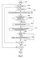
- FIG. 4is a flow diagram of the basic operation of an embodiment of the invention.
- FIG. 5is a flow diagram of the use of an embodiment of the invention in performance of a burn-in test
- FIG. 6is a flow diagram of the use of an embodiment of the invention in performance of a compression test
- FIG. 7is a block diagram of an electronic system including a semiconductor device having test circuitry according to the present invention.
- FIG. 8is a diagram of a semiconductor wafer having test circuitry configured according to an embodiment of the present invention.
- FIG. 1A schematic diagram of an embodiment of the present invention is shown in FIG. 1.
- An integrated circuit deviceis indicated at 1
- the integrated circuit device tester used for testing the integrated circuit deviceis indicated at 2 .
- Integrated circuit device tester 2may be used for testing integrated circuit device 1 .
- Integrated circuit device tester 2is configured for sending a test signal on test signal line 21 and a test address signal on test address line 22 .
- the test address signalspecifies the address on integrated circuit device 1 to which the test signal is to be sent.
- Integrated circuit device tester 2is also configured for sending a set signal on set signal line 23 and a set address signal on set address line 24 .
- Lines 21 , 22 , 23 and 24may be single lines or may be buses that carry multiple signals or bits of data.
- the set address signalindicates the address of the nonvolatile memory element which is to be set to indicate whether the device has passed or failed a particular test or test step.
- Integrated circuit device tester 2has the capability of being programmed to perform multiple test steps, at each test step delivering a particular test signal to a particular address or set of addresses and subsequently sending a set signal and set address signal to select the nonvolatile memory device address memory which is to store the results of the test step.
- the set signaldoes not cause the nonvolatile memory element to be set directly, but enables setting of the nonvolatile memory element by circuitry on integrated circuit device 1 .
- Integrated circuit device tester 2performs similarly to testers currently used in integrated circuit device testing. However, integrated circuit device tester 2 does not need to perform many of the functions conventionally performed by prior testers. For example, without limitation, integrated circuit device tester 2 does not need to perform the functions of reading values from integrated circuit device 1 , comparing these values with expected values and, based on the results of the comparison, generating an instruction for setting a fuse or other nonvolatile memory element on integrated circuit device 1 .
- integrated circuit device tester 2 used in the practice of the inventioncould be a conventional tester programmed to omit unnecessary functions, but still including the detectors, comparators and other hardware which may be used in reading and comparison steps, or it could be a redesigned tester which did not include the detectors, comparators and other hardware rendered superfluous by the present invention.
- Integrated circuit device 1may be a memory device such as a Dynamic Random Access Memory (DRAM), Static Random Access Memory (SRAM), or Video Random Access Memory (VRAM), FLASH or other nonvolatile memory devices, a microprocessor, microcontroller, memory controller, Application Specific Integrated Circuit (ASIC) or other device which is to undergo a test sequence.
- Integrated circuit device 1may include various elements depending upon the type of the device. However, only those elements relevant to the functioning of the test circuitry of the present invention are shown in the Figures. Referring now to FIG.
- integrated circuit device 1includes test circuitry 106 (surrounded by a dashed line) which includes send/receive locations 10 , comparator circuit 11 , at least one test latch 12 , set logic 13 , and nonvolatile memory elements 14 .
- the comparator circuit 11 , test latch 12 , and set logic 13may be included in integrated circuit device 1 in order to carry out the invention and may not be involved in its regular operation. However, it is contemplated that circuit elements used in the regular operation of the integrated circuit device may also be used in the practice of the invention.
- Test latch 12is a latch element capable of latching at least two voltage levels (“logic high” or “logic low”). Various types of latches and latch circuits are well known to those of ordinary skill in the art.
- Nonvolatile memory elements 14 used in the practice of the inventionmay be existing nonvolatile memory elements already present on integrated circuit device 1 or may be included in integrated circuit device 1 specifically for use in the invention.
- Send/receive locations 10may be memory locations if integrated circuit device 1 is a memory device, or they may be inputs and outputs to an integrated circuit if integrated circuit device 1 is something other than a memory device, for example, a microprocessor, microcontroller, memory controller, ASIC, etc.
- Send/receive locations 10are employed in the normal functioning of integrated circuit 1 , whereas other components of test circuitry 106 are included for testing purposes and may not be used in routine operation of the integrated circuit.
- Integrated circuit device 1may include multiple send/receive locations 10 . At a given test step, the send/receive location to be tested is selected according to the test address signal sent on test address line 22 by the integrated circuit device tester 2 .
- Each send/receive location 10may contain one bit or multiple bits (for example, a byte or 8 bits).
- a test signalis sent to the selected send/receive location 10 on input line 101 , and the resulting output signal is received by comparator circuit 11 on corresponding output line 102 .
- Input line 101 and output line 102may be either the same or separate lines. If send/receive location 10 contains multiple bits, input line 101 and output line 102 may be either parallel or serial lines.
- Comparator circuit 11performs a comparison between the value received from the selected send/receive location 10 and the value expected to be obtained from a properly functioning device.
- the value read from the memory locationshould be the same as the value written to the memory location. If a device other than a memory device is being tested, it may be the case that the output value from a particular address will not be the same as that input to the location. However, if the device is functioning properly, a particular output will always correspond to a particular input.
- the comparator circuit 11may store (e.g., latch) the current test value for use as the expected value if a memory device is being tested or it may receive an expected value sent from integrated circuit device tester 2 separate from the test signal. As a further alternative, the expected value may be preset in the device according to a predetermined design rule.
- comparator circuit 11may not truly perform a comparison between the output and the expected value. Since the expected value is always the same, comparator circuit 11 need only be configured so that one output value causes the latch to be set and the other causes it to be unset. This approach would have application primarily in the testing of memory devices.
- Test latch 12may be set depending on whether or not the output from the send/receive location matches the expected value.
- the latch settingpreferably represents the pass or fail status of the test.
- Test latch 12is connected to set logic 13 via latch signal line 15 .
- set logic 13receives an enable signal on latch signal line 15 .
- integrated circuit device tester 2sends a set signal on set signal line 23 and a set address signal on set address line 24 . If both an enable signal and a set signal are received by set logic 13 , the nonvolatile memory element 14 addressed by the set address signal is set by a signal on line 140 , thereby providing a permanent record on the integrated circuit device 1 of the outcome of the test step.
- the nonvolatile memory elements 14remain unset (i.e., set at its original value) if no enable signal is received at the time a set signal is received by set logic 13 . It would also be possible to configure test latch 12 so that an enable signal is sent on latch signal line 15 when test latch 12 is set to a logic low value.
- Nonvolatile memory elements 14may include, without limitation, laser or electrical fuses, antifuses, FLASH memory cells, FERAM memory cells, or other nonvolatile memory elements, which may be set to at least two states (e.g., blown or unblown in the case of fuses or antifuses, programmed or unprogrammed in the case of FLASH memory cells, or logic high and logic low for other types of memory elements), one of which may represent a passing test result and one of which may represent a fail test result.
- Existing semiconductor devicesconventionally include enough nonvolatile memory elements for storing data regarding device test results according to the method of the invention without adding additional elements. However, it is preferred that additional, dedicated nonvolatile memory elements be added.
- Integrated circuit device 1may include multiple nonvolatile memory elements.
- Nonvolatile memory elementsare preferably addressable, being accessed with the use of an address signal sent from integrated circuit device tester 2 .
- nonvolatile memory elementscould be accessed by dedicated lines or by other means, rather than being addressable.
- test latch 12By first setting test latch 12 , and subsequently setting nonvolatile memory element 14 based on the value of test latch 12 , the steps of performing a comparison and obtaining a test result are separated from the step of storing the test result in the nonvolatile memory element 14 . It may be advantageous to separate these steps because the same inputs or signal lines may be used in the different steps; thus, separating the steps allows few inputs or lines to be used.
- test latch 12As discussed above, the setting of test latch 12 , and subsequently the setting of a selected nonvolatile memory element 14 , represent the result of a given test step.
- the relationship between the test result and the setting of nonvolatile memory element 14will generally follow a predetermined rule.
- the rulewill be that for a particular test result, the latch will always be set to a particular value.
- comparator circuit 11may be configured to set test latch 12 to a logical high value if the value on output line 102 matches the expected value, i.e., the test step is passed, and a logical low value if the value on output line 102 does not match the expected value, i.e., the test step is failed.
- comparator circuit 11may be configured so that test latch 12 is set to a logical high value if the output does not match the expected value, i.e., the test step has been failed, and to a logical low value if the test step is passed.
- the value to which nonvolatile memory element 14 is setthen corresponds to the value to which test latch 12 is set, so that nonvolatile memory element 14 is blown, set or programmed, depending on the type of nonvolatile memory element when test latch 12 is set high and left unblown, unset or unprogrammed when test latch 12 is set low.
- nonvolatile memory element 14could be blown, set or programmed when test latch 12 is set low, and vise versa.
- comparator circuit 11 and set logic 13may be configured so that the setting of a nonvolatile memory element 14 is a function of both the result of the test step and the particular test step.
- a nonvolatile memory element 14may be set to a first state if the test is passed and a second state if the test is failed, while at other test steps a nonvolatile memory element 14 may be set to a second state if the test is passed and a first state if the test is failed.
- passing results for sequential test stepscould be represented by a pattern of alternating first and second states.
- a device which has passed all testsis expected to have nonvolatile memory elements set in a predetermined pattern of first and second states.
- the advantage of this approachis that the pattern of first and second states corresponding to a known good device is likely to be obtained only when the device has been properly connected to the test equipment, received appropriate test signals, and passed all tests.
- pass resultsare represented with a single nonvolatile memory setting, false pass results may be obtained if a device has all nonvolatile memory locations set to the same value prior to testing and the original settings are not changed during testing because the device is not properly connected to the semiconductor device.
- test resultsare stored directly in nonvolatile memory elements without the intermediate step of storing the results first in a latch.
- the general concept of storing test results in nonvolatile memory elements without intermediate storage in a latchis already known in the prior art.
- the results of each test stepmay be represented in the setting of a selected nonvolatile memory element 14 according to a predetermined rule.
- Either one or both of comparator circuit 11 or set logic 13may include circuitry which implements said predetermined rule.
- integrated circuit device 1includes a single test latch 12 .
- test latch 12temporarily stores the result of the current test step and, as described above, enables the setting of a nonvolatile memory element 14 to permanently store the result of the test step.
- test latch 12stores the result of one test step at a time, but stores the results of multiple test steps in sequence.
- integrated circuit device 1may include test circuitry 106 (surrounded by dashed line) which is divided into a plurality of subsections or quadrants 1 a , 1 b , 1 c , and 1 d , as depicted in FIG. 2.
- Each subsectionmay include a plurality of send/receive locations 10 a , 10 b , 10 c and 10 d accessed by corresponding input lines 101 a , 101 b , 101 c and 101 d and output lines 102 a , 102 b , 102 c , and 102 d .
- Each quadrantalso includes a comparator circuit 11 a , 11 b , 11 c , or 11 d ; a test latch 12 a , 12 b , 12 c , or 12 d ; a latch signal line 15 a , 15 b , 15 c or 15 d communicating with set logic 13 a , 13 b , 13 c or 13 d .
- Each subsectionmay include a plurality of nonvolatile memory elements 14 a , 14 b , 14 c or 14 d set by lines 140 a , 140 b , 140 c and 140 d , respectively.
- Each test latch 12 a , 12 b , 12 c or 12 dstores the results of the current test step for a particular subsection. Test, test address, set and set address signals are sent on lines 21 , 22 , 23 and 24 as noted previously. Thus each subsection may be tested independently. Although four subsections are depicted in FIG. 2, this is merely exemplary, and the invention may include a larger or smaller number of subsections. If multiple test latches are used, each latch may be independently addressable or may be accessed by means of a dedicated line.
- test circuitry 106(enclosed by dashed line) includes a plurality of subsections 310 a , 310 b , 310 c , 310 d (four are shown here) each containing multiple send/receive locations 10 a , 10 b , 10 c or 10 d , which are accessed by input lines 101 a , 101 b , 101 c and 101 d , respectively; output lines 102 a , 102 b , 102 c and 102 d , respectively; a single comparator circuit 311 ; test latch 312 ; latch signal line 315 ; and set logic 313 .
- test, test address, set and set address signalsare sent on lines 21 , 22 , 23 and 24 , respectively.
- FIGS. 1, 2 and 3may be implemented on a single semiconductor device, with the send/receive locations 10 connected to one or more embodiments of the comparator circuitry 11 , 11 a , 11 b , . . . , 311 a , 311 b , . . . , etc., in order to facilitate testing of the integrated circuit device 1 in a variety of test modes.
- multiple latchesmay be provided on integrated circuit device 1 , or on each subsection of integrated circuit device 1 , so that results of multiple test steps may be stored in latches prior to being stored in nonvolatile memory elements.
- multiple test stepsmay be presented in sequence, and the step of storing the test results in nonvolatile memory elements may be carried out after a sequence of test steps has been presented, rather than after each test step.
- Each latchmay be independently addressable or may be accessed by means of a dedicated line.
- test signalsmay be sent to the device in sequence by the integrated circuit device tester 2 . Values received or read from the device are compared with expected values. The results of the comparisons are ultimately stored on the device in multiple nonvolatile memory elements. Each nonvolatile memory element may represent the results of a particular test or test step. Nonvolatile memory elements may be configured to represent different time points or read points in a test sequence or to represent test results for particular regions of the integrated circuit device. An advantage of storing test results in nonvolatile memory elements on the device is that the nonvolatile memory elements can be checked later to determine results of tests as well as whether a test was carried out properly; the device thus carries its own test history.
- whether the result obtained at a particular test stepmay determine whether a subsequent test step should be carried out. Therefore, in such cases it will be necessary for test equipment, such as integrated circuit device tester 2 , to read test results stored on integrated circuit device 1 so that an appropriate subsequent test step can be determined.
- Prior art integrated circuit device testersinclude the intelligence for determining whether to set a nonvolatile memory element on the integrated circuit device by evaluating the results of tests performed on the device.
- the device being testedincludes the intelligence to determine whether to set a given nonvolatile memory element to represent test results.
- the testersends a set signal and a set address indicating the address of the nonvolatile memory element associated with the current test step for each test step.
- the nonvolatile memory elementis set only if the set signal is present and the latch storing the result of the comparison indicates that the nonvolatile memory element should be set.
- the following examplesdescribe the process by which test steps are delivered, test results are determined, and storage of test results on the semiconductor device in nonvolatile memory elements.
- FIG. 4A flow diagram for the general test procedure used with the embodiment of the invention in FIG. 1 is shown in FIG. 4. This procedure may also be used for testing individual subsections of a device as in FIG. 2.
- a total number of R test stepsare applied, with r representing the current test step.
- Nis the total number of send/receive locations tested, with n representing the current send/receive location.
- the integrated circuit device testersends the address for send/receive location n and test value r which is then stored in send/receive location n of the semiconductor device 1 (step 404 ).
- the comparator circuit for the semiconductor device or semiconductor device subsectionthen performs a comparison between the value received (read) from send/receive location n and the value expected to be obtained from that location in a properly functioning device (step 405 ). If the values do not match, the test latch is set appropriately (step 406 ). If the values do not match, control goes directly to step 407 , in which the integrated circuit device tester sends a set signal and a set address signal to the semiconductor device. At step 408 , set logic on the semiconductor device determines whether a set signal is present and the test latch has been set. If so, nonvolatile memory device r,n is set at step 409 .
- step 410the device tester checks whether the send/receive location being tested is the last send/receive location. If not, control returns to step 403 and the tester delivers the test step to the next send/receive location. If at step 410 it is determined that the last send/receive location has been reached (that is, all send/receive locations have been tested with the current test step), the tester checks whether the last test step has been reached (step 411 ). If not, control returns to step 402 and the next test step is delivered. If the last test step has been delivered, testing is ended (step 412 ). It is preferred that a separate nonvolatile memory element is used at step 409 to store the result of each test step.
- a single latchis used to store a value indicating whether setting of the nonvolatile memory element associated with that test step is to be enabled.
- the same latchmay be used to enable setting of different nonvolatile memory elements associated with the different test steps.
- FIG. 5A flow diagram for burn-in testing is provided in FIG. 5. This test procedure may be used with a device as depicted in FIG. 1, or subsection of a device as depicted in FIG. 2.
- a particular data valueis written repeatedly to a particular send/receive location, typically under extreme conditions of temperature, voltage, timing, etc., in an effort to cause the failure of a device having some flaw that would cause it to fail early in its life cycle.
- Dataare read from a given send/receive location at each repetition or at specified intervals in order to determine if and when failure occurs.
- Multiple nonvolatile memory elementsmay be used to store the pass/fail information for the different read points, with each nonvolatile memory element representing one read point.
- Read pointsmay be used to represent specific time intervals throughout a burn in test such that, for example, a nonvolatile memory element is set after each hour of burn-in testing.
- Nonvolatile memory elementsmay also be used to store the number of the current read point, so that a record of the number of repetitions is stored on the device at all times during testing.
- Rrepresents the total number of test steps
- rthe current test step
- Nrepresents the total number of send/receive locations tested
- nthe current send/receive location
- Pthe total number of repetitions
- pthe number of the current repetition.
- the testersends a test value r to send/receive location n (step 505 ).
- the semiconductor devicecompares the test value with the value read from send/receive location n (step 506 ). If a mismatch occurs, indicating a failure, the test latch is set at step 507 . If the values match, step 507 is bypassed.
- the testernext sends a set signal and a set address corresponding to the nonvolatile memory elements designated to store the test result for the current repetition p (step 508 ). If a set signal is present and the test latch has been set (step 509 ), the semiconductor device causes the selected nonvolatile memory element to be set (step 510 ). Control returns to step 504 from step 511 until a total of P repetitions of the test signal have been delivered. Testing continues until all send/receive locations have been tested (step 512 ) and all test sequences have been delivered ( 513 ).
- Compression testingis used to shorten test times by simultaneously testing several identical subsections of a semiconductor device, or several regions on different devices of the same type.
- the block diagram of FIG. 3depicts a semiconductor device having multiple subsections (four in this example, but any number greater than one could be used) and comparator circuit and set logic configured for use in compression testing.
- the same data valuesare simultaneously written to multiple subsections of the device (for example, to memory cells in multiple subsections of the device) and then data are read back from each subsection and values read from all subsections are compared. Matching values indicate that the test was passed if a mismatch is detected, this indicates that some of the tested areas are not functioning properly and the test has been failed.
- FIG. 6A flow diagram for compression testing is given in FIG. 6.
- Rrepresents the total number of test steps, r the current test step, N the total number of send/receive locations tested in each subsection of the semiconductor device, and n 1 , n 2 , n 3 . . . n m the current send/receive location in subsections 1 . . . m of the semiconductor device.
- the test procedurebegins at step 601 .
- test value ris simultaneously sent to send/receive locations n 1 , n 2 , n 3 . . . n m .
- the semiconductor devicecompares the values received from send/receive locations n 1 , n 2 , n 3 . . . n m . If a mismatch is detected, a test latch is set (step 606 ). If all values match, step 606 is bypassed.
- the testerthen sends a set signal and an address signal for nonvolatile memory element r,n (step 607 ). If a set signal is present and the test latch is set (step 608 ), the semiconductor device sets nonvolatile memory element r,n (step 609 ). Control returns to step 603 from step 610 until a total of N send/receive locations have been tested in each subsection with test step r. Testing continues until all test steps have been delivered ( 611 ).
- FIG. 7shows a block diagram of an electronic system 700 which includes components having one or more test circuits 106 configured according to one or more embodiments of the present invention.
- the electronic system 700includes a processor 704 for performing various computing functions, such as executing specific software to perform specific calculations or tasks. Additionally, the electronic system 700 includes one or more input devices 708 , such as a keyboard or mouse, coupled to the processor 704 to allow an operator to interface with the electronic system 700 .
- the electronic system 700also includes one or more output devices 710 coupled to the processor 704 , such output devices including but not limited to a printer, a video terminal or a network connection.
- One or more data storage devices 712are also conventionally coupled to the processor 704 to store or retrieve data from external storage media (not shown).
- Examples of conventional storage devices 712include hard and floppy disks, tape cassettes, compact disks and optical memory.
- the processor 704is also conventionally coupled to a cache memory 714 , which is usually static random access memory (“SRAM”), and to DRAM 702 . It will be understood, however, that the test circuit 106 configured according to one or more of the embodiments of the present invention may be incorporated into any one of the cache, DRAM, input, output, storage and processor devices 714 , 702 , 708 , 710 , 712 and 704 .
- test circuit 106may be fabricated on the surface of a semiconductor wafer 816 of silicon, gallium arsenide, or indium phosphide in accordance with one or more embodiments of the present invention.
- a semiconductor wafer 816 of silicon, gallium arsenide, or indium phosphidein accordance with one or more embodiments of the present invention.
- the test circuit 106may be fabricated on semiconductor substrates other than a wafer, such as a Silicon-on-Insulator (SOI) substrate, a Silicon-on-Glass (SOG) substrate, a Silicon-on-Sapphire (SOS) substrate, or other semiconductor material layers on supporting substrates.
- SOISilicon-on-Insulator
- SOGSilicon-on-Glass
- SOSSilicon-on-Sapphire
- the principles of the present inventionmay be used in conjunction with any number of the various semiconductor test methods known in the art and is not limited to those test methods described herein, or to the testing of memory devices.
- testing devicesmay be simplified. Additionally, by storing passing test result data as a mixed code of two different states rather than merely as a series of entirely the first state or the second state, the success of a series of tests may more accurately be determined.
Landscapes
- Engineering & Computer Science (AREA)
- General Engineering & Computer Science (AREA)
- Physics & Mathematics (AREA)
- General Physics & Mathematics (AREA)
- Computer Hardware Design (AREA)
- Microelectronics & Electronic Packaging (AREA)
- Tests Of Electronic Circuits (AREA)
Abstract
Description
- This application is a continuation of application Ser. No. 09/651,858, filed Aug. 30, 2000, pending.[0001]
- 1. Field of the Invention[0002]
- The present invention relates to integrated circuit test circuits and methods. In particular, the present invention relates to storage of test result data on an integrated circuit device in nonvolatile memory elements and, most particularly, to the inclusion of logic in the integrated circuit device for determining the results of device tests and enabling the storage of test results in the nonvolatile memory elements.[0003]
- Statement of the Art[0004]
- Semiconductor integrated circuit devices are manufactured on wafers or other substrates of semiconductor material. Conventionally, many devices are manufactured on a single wafer and individual devices or groups of devices are cut from the wafer and packaged. The devices are tested at various points during the manufacturing process, e.g., with electrical probes while they are still on the wafer, in die form (after singulation but prior to packaging) and after packaging.[0005]
- During testing, a particular signal or combination of signals is input to the device and the output value or values read from the device are compared with values expected to be obtained from a properly functioning device. Tests may involve a particular signal or combination of signals being delivered repetitively, perhaps under extreme environmental conditions (temperature, voltage, etc.) in order to identify a device which would fail after a shorter than usual period of use (“burn-in” testing). Other tests may involve a number of different signals or signal combinations delivered in sequence. One method for testing a memory device is to deliver the same signal/signal combination to multiple identical subsections of the device simultaneously and compare the values read from the subsections (“compression testing”). If all of the respective, read values match, the test has been passed, while a mismatch between respective values read from any of the subsections indicates a device malfunction and failure of the test.[0006]
- A particular test or test sequence often includes multiple test steps. Moreover, a complete test flow will often require that devices move from one piece of test equipment to another. For example, a first piece of test equipment and test fixtures may be utilized for probe: testing, another for burn-in testing and yet another for packaged device testing after burn-in.[0007]
- After a particular test or test sequence has been completed, devices which have failed some or all of a test may be separated from the good devices. However, a device which has failed one portion of the test sequence may pass subsequent test sequences, so if it is erroneously placed into the “good” bin and then passes subsequent tests it may eventually be classified and sold as fully functional. One way to avoid this type of error is to store information regarding the test history of the device on the device itself in nonvolatile memory elements. One example describing storage of test results in nonvolatile memory on a semiconductor device is co-pending U.S. patent application Ser. No. 08/946,027, the disclosure of which is hereby incorporated herein by reference.[0008]
- Test equipment used for testing integrated circuit devices conventionally transmits a test signal and then receives an output signal from the integrated circuit device. The test equipment then compares the output signal from the integrated circuit device with the value expected to be obtained from a properly functioning device and sends an instruction to the device which causes a specific nonvolatile memory element to be set to indicate either pass or fail of the test step. A series of nonvolatile memory elements may be set to indicate the results of a series of tests or test steps. The tester thus must include detectors and comparators so that it can read the output signal and perform a comparison to determine passage or failure of the test.[0009]
- It would be advantageous to decrease the cost and complexity of the tester by eliminating the need for detectors and comparators on the test equipment.[0010]
- It would be advantageous to eliminate the need for intelligence in device test equipment, by instead placing intelligence on the device being tested.[0011]
- It would be desirable to provide for the storage of information concerning correct application of test sequences to the device on the device itself.[0012]
- These and other advantages are provided by the invention.[0013]
- The present invention includes a method and system for storing semiconductor device test results on a tested device, using on-device test circuitry for the determination of test results and control of test result storage. The semiconductor device, which may be a memory device, a microprocessor, or other semiconductor device, includes a plurality of nonvolatile memory elements which are set to indicate the results of a series of multiple tests or test steps. The semiconductor device may also include comparator circuitry, which compares test signals sent to the semiconductor device from a tester with data values read from the semiconductor device following receipt of the test signals, or which performs a comparison between data values read from multiple regions of a device, to determine correct functioning of the device. The semiconductor device includes a latch which is set to indicate passage or failure of the test. The latch enables circuitry which causes a nonvolatile memory element to be set upon receipt of an instruction from the tester. The latch, and subsequently the nonvolatile memory element, are set to represent the test results according to a predetermined rule. Typically, one logic level is latched to represent passage of a test and another is used to represent failure of the test. For example, logic high could represent pass and logic low would then represent fail or, alternatively, logic low could represent pass and logic high represent fail. Similarly, the nonvolatile memory element is set to one state to represent passage of a test and another to represent failure of the test.[0014]
- By locating the circuitry that controls setting of memory elements to represent test results on the device being tested, the tester equipment does not need to receive values from the device being tested, perform a comparison between test values and received values to determine the outcome of the test, or determine whether a memory element should be set to store the test result. The tester needs only to transmit test signals and set signals to the semiconductor device, without receiving any values back from the semiconductor device. Accordingly, the design and construction of the test equipment can be simplified considerably.[0015]
- In one embodiment of the invention, a rule used to determine the settings of latches and nonvolatile memory elements to represent pass/fail status is dependent on the test or test step being performed. That is, for certain tests/test steps a first state would represent pass and a second state would represent fail, while for other tests/test steps the second state would represent pass and the first state would represent fail. Therefore, a device which had passed all tests would be expected to have nonvolatile memory elements set in a predetermined pattern of first and second states. The pattern of first and second states corresponding to a known good device is obtained only when the device has been properly connected to the test equipment, received appropriate test signals and passed all tests.[0016]
- FIG. 1 is a block diagram of an integrated circuit tester and an integrated circuit according to an embodiment of the invention;[0017]
- FIG. 2 is a block diagram of an integrated circuit having a plurality of subsections, each including comparator and set circuitry, according to an embodiment of the invention;[0018]
- FIG. 3 is a block diagram of an integrated circuit having a plurality of subsections but a single comparator circuit and set circuit according to a further embodiment of the invention;[0019]
- FIG. 4 is a flow diagram of the basic operation of an embodiment of the invention;[0020]
- FIG. 5 is a flow diagram of the use of an embodiment of the invention in performance of a burn-in test;[0021]
- FIG. 6 is a flow diagram of the use of an embodiment of the invention in performance of a compression test;[0022]
- FIG. 7 is a block diagram of an electronic system including a semiconductor device having test circuitry according to the present invention; and[0023]
- FIG. 8 is a diagram of a semiconductor wafer having test circuitry configured according to an embodiment of the present invention.[0024]
- A schematic diagram of an embodiment of the present invention is shown in FIG. 1. An integrated circuit device is indicated at[0025]1, and the integrated circuit device tester used for testing the integrated circuit device is indicated at2.
- Integrated Circuit Device Tester[0026]
- Integrated[0027]
circuit device tester 2 may be used for testingintegrated circuit device 1. Integratedcircuit device tester 2 is configured for sending a test signal ontest signal line 21 and a test address signal ontest address line 22. The test address signal specifies the address onintegrated circuit device 1 to which the test signal is to be sent. Integratedcircuit device tester 2 is also configured for sending a set signal onset signal line 23 and a set address signal on setaddress line 24.Lines circuit device tester 2 has the capability of being programmed to perform multiple test steps, at each test step delivering a particular test signal to a particular address or set of addresses and subsequently sending a set signal and set address signal to select the nonvolatile memory device address memory which is to store the results of the test step. The set signal does not cause the nonvolatile memory element to be set directly, but enables setting of the nonvolatile memory element by circuitry onintegrated circuit device 1. - Integrated[0028]
circuit device tester 2 performs similarly to testers currently used in integrated circuit device testing. However, integratedcircuit device tester 2 does not need to perform many of the functions conventionally performed by prior testers. For example, without limitation, integratedcircuit device tester 2 does not need to perform the functions of reading values fromintegrated circuit device 1, comparing these values with expected values and, based on the results of the comparison, generating an instruction for setting a fuse or other nonvolatile memory element onintegrated circuit device 1. Thus, integratedcircuit device tester 2 used in the practice of the invention could be a conventional tester programmed to omit unnecessary functions, but still including the detectors, comparators and other hardware which may be used in reading and comparison steps, or it could be a redesigned tester which did not include the detectors, comparators and other hardware rendered superfluous by the present invention. - Integrated Circuit Device[0029]
- [0030]
Integrated circuit device 1 may be a memory device such as a Dynamic Random Access Memory (DRAM), Static Random Access Memory (SRAM), or Video Random Access Memory (VRAM), FLASH or other nonvolatile memory devices, a microprocessor, microcontroller, memory controller, Application Specific Integrated Circuit (ASIC) or other device which is to undergo a test sequence.Integrated circuit device 1 may include various elements depending upon the type of the device. However, only those elements relevant to the functioning of the test circuitry of the present invention are shown in the Figures. Referring now to FIG. 1, integratedcircuit device 1 includes test circuitry106 (surrounded by a dashed line) which includes send/receivelocations 10,comparator circuit 11, at least onetest latch 12, setlogic 13, andnonvolatile memory elements 14. Thecomparator circuit 11,test latch 12, and setlogic 13 may be included inintegrated circuit device 1 in order to carry out the invention and may not be involved in its regular operation. However, it is contemplated that circuit elements used in the regular operation of the integrated circuit device may also be used in the practice of the invention.Test latch 12 is a latch element capable of latching at least two voltage levels (“logic high” or “logic low”). Various types of latches and latch circuits are well known to those of ordinary skill in the art. One example of a latch suitable for use in the present invention is an S-R NOR latch.Nonvolatile memory elements 14 used in the practice of the invention may be existing nonvolatile memory elements already present onintegrated circuit device 1 or may be included inintegrated circuit device 1 specifically for use in the invention. - Send/receive[0031]
locations 10 may be memory locations ifintegrated circuit device 1 is a memory device, or they may be inputs and outputs to an integrated circuit ifintegrated circuit device 1 is something other than a memory device, for example, a microprocessor, microcontroller, memory controller, ASIC, etc. Send/receivelocations 10 are employed in the normal functioning ofintegrated circuit 1, whereas other components oftest circuitry 106 are included for testing purposes and may not be used in routine operation of the integrated circuit.Integrated circuit device 1 may include multiple send/receivelocations 10. At a given test step, the send/receive location to be tested is selected according to the test address signal sent ontest address line 22 by the integratedcircuit device tester 2. Alternatively, it would be possible to access a given send/receivelocation 10 by means of a direct line without the use of addressing. Each send/receivelocation 10 may contain one bit or multiple bits (for example, a byte or 8 bits). A test signal is sent to the selected send/receivelocation 10 oninput line 101, and the resulting output signal is received bycomparator circuit 11 oncorresponding output line 102.Input line 101 andoutput line 102 may be either the same or separate lines. If send/receivelocation 10 contains multiple bits,input line 101 andoutput line 102 may be either parallel or serial lines.Comparator circuit 11 performs a comparison between the value received from the selected send/receivelocation 10 and the value expected to be obtained from a properly functioning device. For example, if the addressed send/receivelocation 10 is a memory location, the value read from the memory location should be the same as the value written to the memory location. If a device other than a memory device is being tested, it may be the case that the output value from a particular address will not be the same as that input to the location. However, if the device is functioning properly, a particular output will always correspond to a particular input. Thecomparator circuit 11 may store (e.g., latch) the current test value for use as the expected value if a memory device is being tested or it may receive an expected value sent from integratedcircuit device tester 2 separate from the test signal. As a further alternative, the expected value may be preset in the device according to a predetermined design rule. In this case,comparator circuit 11 may not truly perform a comparison between the output and the expected value. Since the expected value is always the same,comparator circuit 11 need only be configured so that one output value causes the latch to be set and the other causes it to be unset. This approach would have application primarily in the testing of memory devices. - [0032]
Test latch 12 may be set depending on whether or not the output from the send/receive location matches the expected value. The latch setting preferably represents the pass or fail status of the test.Test latch 12 is connected to setlogic 13 vialatch signal line 15. When test latch12 is set to a logical high value, setlogic 13 receives an enable signal onlatch signal line 15. At the end of a test step, integratedcircuit device tester 2 sends a set signal onset signal line 23 and a set address signal on setaddress line 24. If both an enable signal and a set signal are received byset logic 13, thenonvolatile memory element 14 addressed by the set address signal is set by a signal online 140, thereby providing a permanent record on theintegrated circuit device 1 of the outcome of the test step. Thenonvolatile memory elements 14 remain unset (i.e., set at its original value) if no enable signal is received at the time a set signal is received byset logic 13. It would also be possible to configuretest latch 12 so that an enable signal is sent onlatch signal line 15 whentest latch 12 is set to a logic low value. - [0033]
Nonvolatile memory elements 14 may include, without limitation, laser or electrical fuses, antifuses, FLASH memory cells, FERAM memory cells, or other nonvolatile memory elements, which may be set to at least two states (e.g., blown or unblown in the case of fuses or antifuses, programmed or unprogrammed in the case of FLASH memory cells, or logic high and logic low for other types of memory elements), one of which may represent a passing test result and one of which may represent a fail test result. Existing semiconductor devices conventionally include enough nonvolatile memory elements for storing data regarding device test results according to the method of the invention without adding additional elements. However, it is preferred that additional, dedicated nonvolatile memory elements be added.Integrated circuit device 1 may include multiple nonvolatile memory elements. Nonvolatile memory elements are preferably addressable, being accessed with the use of an address signal sent from integratedcircuit device tester 2. However, in the alternative, nonvolatile memory elements could be accessed by dedicated lines or by other means, rather than being addressable. - By first[0034]
setting test latch 12, and subsequently settingnonvolatile memory element 14 based on the value oftest latch 12, the steps of performing a comparison and obtaining a test result are separated from the step of storing the test result in thenonvolatile memory element 14. It may be advantageous to separate these steps because the same inputs or signal lines may be used in the different steps; thus, separating the steps allows few inputs or lines to be used. - As discussed above, the setting of[0035]
test latch 12, and subsequently the setting of a selectednonvolatile memory element 14, represent the result of a given test step. The relationship between the test result and the setting ofnonvolatile memory element 14 will generally follow a predetermined rule. In the simplest case, the rule will be that for a particular test result, the latch will always be set to a particular value. For example,comparator circuit 11 may be configured to settest latch 12 to a logical high value if the value onoutput line 102 matches the expected value, i.e., the test step is passed, and a logical low value if the value onoutput line 102 does not match the expected value, i.e., the test step is failed. Alternatively,comparator circuit 11 may be configured so thattest latch 12 is set to a logical high value if the output does not match the expected value, i.e., the test step has been failed, and to a logical low value if the test step is passed. The value to whichnonvolatile memory element 14 is set then corresponds to the value to which test latch12 is set, so thatnonvolatile memory element 14 is blown, set or programmed, depending on the type of nonvolatile memory element whentest latch 12 is set high and left unblown, unset or unprogrammed whentest latch 12 is set low. Alternatively,nonvolatile memory element 14 could be blown, set or programmed whentest latch 12 is set low, and vise versa. - In one embodiment of the invention,[0036]
comparator circuit 11 and setlogic 13 may be configured so that the setting of anonvolatile memory element 14 is a function of both the result of the test step and the particular test step. At certain test steps anonvolatile memory element 14 may be set to a first state if the test is passed and a second state if the test is failed, while at other test steps anonvolatile memory element 14 may be set to a second state if the test is passed and a first state if the test is failed. For example, passing results for sequential test steps could be represented by a pattern of alternating first and second states. In this embodiment of the invention, a device which has passed all tests is expected to have nonvolatile memory elements set in a predetermined pattern of first and second states. The advantage of this approach is that the pattern of first and second states corresponding to a known good device is likely to be obtained only when the device has been properly connected to the test equipment, received appropriate test signals, and passed all tests. In contrast, if pass results are represented with a single nonvolatile memory setting, false pass results may be obtained if a device has all nonvolatile memory locations set to the same value prior to testing and the original settings are not changed during testing because the device is not properly connected to the semiconductor device. - Although it is preferred to include the step of setting a latch intermediate the steps of determining a test result and storing the test result in a nonvolatile memory element for the reasons noted previously, the concept of storing test results as a function of test step and test result could be applied in a system in which test results were stored directly in nonvolatile memory elements without the intermediate step of storing the results first in a latch. The general concept of storing test results in nonvolatile memory elements without intermediate storage in a latch is already known in the prior art.[0037]
- As described above, the results of each test step may be represented in the setting of a selected[0038]
nonvolatile memory element 14 according to a predetermined rule. Either one or both ofcomparator circuit 11 or setlogic 13 may include circuitry which implements said predetermined rule. - In the embodiment of the invention depicted in FIG. 1, integrated[0039]
circuit device 1 includes asingle test latch 12. At each test step,test latch 12 temporarily stores the result of the current test step and, as described above, enables the setting of anonvolatile memory element 14 to permanently store the result of the test step. Thus,test latch 12 stores the result of one test step at a time, but stores the results of multiple test steps in sequence. It is contemplated, however, that in other embodiments of the invention, integratedcircuit device 1 may include test circuitry106 (surrounded by dashed line) which is divided into a plurality of subsections orquadrants locations input lines output lines comparator circuit test latch latch signal line set logic nonvolatile memory elements lines lines - In yet another alternative embodiment of the invention, as depicted in FIG. 3, test circuitry[0040]106 (enclosed by dashed line) includes a plurality of
subsections locations input lines output lines single comparator circuit 311;test latch 312;latch signal line 315; and setlogic 313. This permits a comparison to be made between the values received from send/receive locations in the different subsections of the device. Multiplenonvolatile memory elements 14 are also included accessible bylines 140. Test, test address, set and set address signals are sent onlines - The different embodiments of the invention are particularly suited for different types of device testing, as will be described hereinbelow. It will be appreciated that the embodiments of the invention depicted in FIGS. 1, 2 and[0041]3 may be implemented on a single semiconductor device, with the send/receive
locations 10 connected to one or more embodiments of thecomparator circuitry integrated circuit device 1 in a variety of test modes. - In yet another embodiment of the invention, multiple latches may be provided on[0042]
integrated circuit device 1, or on each subsection ofintegrated circuit device 1, so that results of multiple test steps may be stored in latches prior to being stored in nonvolatile memory elements. Thus, multiple test steps may be presented in sequence, and the step of storing the test results in nonvolatile memory elements may be carried out after a sequence of test steps has been presented, rather than after each test step. Each latch may be independently addressable or may be accessed by means of a dedicated line. - Testing Procedure[0043]
- During testing of an[0044]
integrated circuit device 1, a variety of test signals may be sent to the device in sequence by the integratedcircuit device tester 2. Values received or read from the device are compared with expected values. The results of the comparisons are ultimately stored on the device in multiple nonvolatile memory elements. Each nonvolatile memory element may represent the results of a particular test or test step. Nonvolatile memory elements may be configured to represent different time points or read points in a test sequence or to represent test results for particular regions of the integrated circuit device. An advantage of storing test results in nonvolatile memory elements on the device is that the nonvolatile memory elements can be checked later to determine results of tests as well as whether a test was carried out properly; the device thus carries its own test history. - In some cases, whether the result obtained at a particular test step may determine whether a subsequent test step should be carried out. Therefore, in such cases it will be necessary for test equipment, such as integrated[0045]
circuit device tester 2, to read test results stored on integratedcircuit device 1 so that an appropriate subsequent test step can be determined. - Prior art integrated circuit device testers include the intelligence for determining whether to set a nonvolatile memory element on the integrated circuit device by evaluating the results of tests performed on the device. With the present invention, the device being tested includes the intelligence to determine whether to set a given nonvolatile memory element to represent test results. The tester sends a set signal and a set address indicating the address of the nonvolatile memory element associated with the current test step for each test step. However, the nonvolatile memory element is set only if the set signal is present and the latch storing the result of the comparison indicates that the nonvolatile memory element should be set. The following examples describe the process by which test steps are delivered, test results are determined, and storage of test results on the semiconductor device in nonvolatile memory elements.[0046]
- A flow diagram for the general test procedure used with the embodiment of the invention in FIG. 1 is shown in FIG. 4. This procedure may also be used for testing individual subsections of a device as in FIG. 2. In this example, a total number of R test steps are applied, with r representing the current test step. N is the total number of send/receive locations tested, with n representing the current send/receive location. The general testing procedure begins at[0047]401 and is carried out for values of r=1 to R (step402) and n=1 to N (step403). The integrated circuit device tester sends the address for send/receive location n and test value r which is then stored in send/receive location n of the semiconductor device1 (step404). The comparator circuit for the semiconductor device or semiconductor device subsection then performs a comparison between the value received (read) from send/receive location n and the value expected to be obtained from that location in a properly functioning device (step405). If the values do not match, the test latch is set appropriately (step406). If the values do not match, control goes directly to step407, in which the integrated circuit device tester sends a set signal and a set address signal to the semiconductor device. At
step 408, set logic on the semiconductor device determines whether a set signal is present and the test latch has been set. If so, nonvolatile memory device r,n is set atstep 409. If not, control goes directly to step410, in which the device tester checks whether the send/receive location being tested is the last send/receive location. If not, control returns to step403 and the tester delivers the test step to the next send/receive location. If atstep 410 it is determined that the last send/receive location has been reached (that is, all send/receive locations have been tested with the current test step), the tester checks whether the last test step has been reached (step411). If not, control returns to step402 and the next test step is delivered. If the last test step has been delivered, testing is ended (step412). It is preferred that a separate nonvolatile memory element is used atstep 409 to store the result of each test step. At each test step, a single latch is used to store a value indicating whether setting of the nonvolatile memory element associated with that test step is to be enabled. On subsequent test steps, the same latch may be used to enable setting of different nonvolatile memory elements associated with the different test steps. There may be a single latch for each device for storing test step results, as shown in FIG. 1. Alternatively, it may be desirable to test several sections of a semiconductor device (e.g., subarrays of memory) separately and store test results in a separate latch for each section, in which case the semiconductor device as a whole would include at least as many latches as there were sections, as shown in FIG. 2. Although the flow diagram for the standard test in FIG. 4 shows the tester cycling through all send/receive locations for a given test step before moving on to the next test step, it may also be preferable to cycle through all test steps at a particular send/receive location before moving to the next send/receive location, that is, to place the loop beginning atstep 403 outside the loop beginning atstep 402. - A flow diagram for burn-in testing is provided in FIG. 5. This test procedure may be used with a device as depicted in FIG. 1, or subsection of a device as depicted in FIG. 2. During burn-in testing, a particular data value is written repeatedly to a particular send/receive location, typically under extreme conditions of temperature, voltage, timing, etc., in an effort to cause the failure of a device having some flaw that would cause it to fail early in its life cycle. Data are read from a given send/receive location at each repetition or at specified intervals in order to determine if and when failure occurs. Multiple nonvolatile memory elements may be used to store the pass/fail information for the different read points, with each nonvolatile memory element representing one read point. Read points may be used to represent specific time intervals throughout a burn in test such that, for example, a nonvolatile memory element is set after each hour of burn-in testing. Nonvolatile memory elements may also be used to store the number of the current read point, so that a record of the number of repetitions is stored on the device at all times during testing. In FIG. 5, R represents the total number of test steps, r the current test step, N represents the total number of send/receive locations tested, n the current send/receive location, P the total number of repetitions, and p the number of the current repetition. The burn-in test procedure begins at[0048]
step 501, and is carried out for values of r=1 to R (step502), n=1 to N (step503), and p=1 to P (step504). At each repetition p, the tester sends a test value r to send/receive location n (step505). The semiconductor device compares the test value with the value read from send/receive location n (step506). If a mismatch occurs, indicating a failure, the test latch is set atstep 507. If the values match,step 507 is bypassed. The tester next sends a set signal and a set address corresponding to the nonvolatile memory elements designated to store the test result for the current repetition p (step508). If a set signal is present and the test latch has been set (step509), the semiconductor device causes the selected nonvolatile memory element to be set (step510). Control returns to step504 fromstep 511 until a total of P repetitions of the test signal have been delivered. Testing continues until all send/receive locations have been tested (step512) and all test sequences have been delivered (513). - Compression testing is used to shorten test times by simultaneously testing several identical subsections of a semiconductor device, or several regions on different devices of the same type. The block diagram of FIG. 3 depicts a semiconductor device having multiple subsections (four in this example, but any number greater than one could be used) and comparator circuit and set logic configured for use in compression testing. The same data values are simultaneously written to multiple subsections of the device (for example, to memory cells in multiple subsections of the device) and then data are read back from each subsection and values read from all subsections are compared. Matching values indicate that the test was passed if a mismatch is detected, this indicates that some of the tested areas are not functioning properly and the test has been failed. If the test has been failed, a latch is set to enable or disable setting of a selected nonvolatile memory element. A flow diagram for compression testing is given in FIG. 6. R represents the total number of test steps, r the current test step, N the total number of send/receive locations tested in each subsection of the semiconductor device, and n[0049]1, n2, n3. . . nmthe current send/receive location in
subsections 1 . . . m of the semiconductor device. In FIG. 6, a semiconductor device with four subsections is depicted, so m=4, but it will be appreciated that this is merely exemplary, and a larger or smaller number of subsections could be used in the practice of the invention. Naturally, at least two subsections must be present in order to perform a comparison. The test procedure begins atstep 601. The test procedure is carried out for values of r=1 to R (step602) and n=1 to N (step603). Atstep 604, test value r is simultaneously sent to send/receive locations n1, n2, n3. . . nm. Atstep 605, the semiconductor device compares the values received from send/receive locations n1, n2, n3. . . nm. If a mismatch is detected, a test latch is set (step606). If all values match,step 606 is bypassed. The tester then sends a set signal and an address signal for nonvolatile memory element r,n (step607). If a set signal is present and the test latch is set (step608), the semiconductor device sets nonvolatile memory element r,n (step609). Control returns to step603 fromstep 610 until a total of N send/receive locations have been tested in each subsection with test step r. Testing continues until all test steps have been delivered (611). - FIG. 7 shows a block diagram of an[0050]
electronic system 700 which includes components having one ormore test circuits 106 configured according to one or more embodiments of the present invention. Theelectronic system 700 includes aprocessor 704 for performing various computing functions, such as executing specific software to perform specific calculations or tasks. Additionally, theelectronic system 700 includes one ormore input devices 708, such as a keyboard or mouse, coupled to theprocessor 704 to allow an operator to interface with theelectronic system 700. Theelectronic system 700 also includes one ormore output devices 710 coupled to theprocessor 704, such output devices including but not limited to a printer, a video terminal or a network connection. One or moredata storage devices 712 are also conventionally coupled to theprocessor 704 to store or retrieve data from external storage media (not shown). Examples ofconventional storage devices 712 include hard and floppy disks, tape cassettes, compact disks and optical memory. Theprocessor 704 is also conventionally coupled to acache memory 714, which is usually static random access memory (“SRAM”), and toDRAM 702. It will be understood, however, that thetest circuit 106 configured according to one or more of the embodiments of the present invention may be incorporated into any one of the cache, DRAM, input, output, storage andprocessor devices - As shown in FIG. 8,[0051]
test circuit 106 may be fabricated on the surface of asemiconductor wafer 816 of silicon, gallium arsenide, or indium phosphide in accordance with one or more embodiments of the present invention. One of ordinary skill in the art will understand how to adapt such design for a specific chip architecture or semiconductor fabrication process. Of course, it should be understood that thetest circuit 106 may be fabricated on semiconductor substrates other than a wafer, such as a Silicon-on-Insulator (SOI) substrate, a Silicon-on-Glass (SOG) substrate, a Silicon-on-Sapphire (SOS) substrate, or other semiconductor material layers on supporting substrates. - As will be clear to one of ordinary skill in the art, the principles of the present invention may be used in conjunction with any number of the various semiconductor test methods known in the art and is not limited to those test methods described herein, or to the testing of memory devices. By including at least one latch circuit within a semiconductor device to indicate whether a nonvolatile memory element should be initiated, testing devices may be simplified. Additionally, by storing passing test result data as a mixed code of two different states rather than merely as a series of entirely the first state or the second state, the success of a series of tests may more accurately be determined.[0052]
- While the present invention has been described and illustrated in terms of certain specific embodiments, those of ordinary skill in the art will understand and appreciate that it is not so limited. Additions to, deletions from and modifications to these specific embodiments may be effected without departing from the scope of the invention as defined by the claims. Furthermore, features and elements from one specific embodiment may be likewise applied to another embodiment without departing from the scope of the invention as defined herein.[0053]
Claims (15)
Priority Applications (2)
| Application Number | Priority Date | Filing Date | Title |
|---|---|---|---|
| US10/794,696US7194667B2 (en) | 2000-08-30 | 2004-03-05 | System for storing device test information on a semiconductor device using on-device logic for determination of test results |
| US11/357,487US20060156136A1 (en) | 2000-08-30 | 2006-02-17 | System for storing device test information on a semiconductor device using on-device logic for determination of test results |
Applications Claiming Priority (2)
| Application Number | Priority Date | Filing Date | Title |
|---|---|---|---|
| US09/651,858US6829737B1 (en) | 2000-08-30 | 2000-08-30 | Method and system for storing device test information on a semiconductor device using on-device logic for determination of test results |
| US10/794,696US7194667B2 (en) | 2000-08-30 | 2004-03-05 | System for storing device test information on a semiconductor device using on-device logic for determination of test results |
Related Parent Applications (1)
| Application Number | Title | Priority Date | Filing Date |
|---|---|---|---|
| US09/651,858ContinuationUS6829737B1 (en) | 2000-08-30 | 2000-08-30 | Method and system for storing device test information on a semiconductor device using on-device logic for determination of test results |
Related Child Applications (1)
| Application Number | Title | Priority Date | Filing Date |
|---|---|---|---|
| US11/357,487ContinuationUS20060156136A1 (en) | 2000-08-30 | 2006-02-17 | System for storing device test information on a semiconductor device using on-device logic for determination of test results |
Publications (2)
| Publication Number | Publication Date |
|---|---|
| US20040181724A1true US20040181724A1 (en) | 2004-09-16 |
| US7194667B2 US7194667B2 (en) | 2007-03-20 |
Family
ID=32962832
Family Applications (3)
| Application Number | Title | Priority Date | Filing Date |
|---|---|---|---|
| US09/651,858Expired - LifetimeUS6829737B1 (en) | 2000-08-30 | 2000-08-30 | Method and system for storing device test information on a semiconductor device using on-device logic for determination of test results |
| US10/794,696Expired - LifetimeUS7194667B2 (en) | 2000-08-30 | 2004-03-05 | System for storing device test information on a semiconductor device using on-device logic for determination of test results |
| US11/357,487AbandonedUS20060156136A1 (en) | 2000-08-30 | 2006-02-17 | System for storing device test information on a semiconductor device using on-device logic for determination of test results |
Family Applications Before (1)
| Application Number | Title | Priority Date | Filing Date |
|---|---|---|---|
| US09/651,858Expired - LifetimeUS6829737B1 (en) | 2000-08-30 | 2000-08-30 | Method and system for storing device test information on a semiconductor device using on-device logic for determination of test results |
Family Applications After (1)
| Application Number | Title | Priority Date | Filing Date |
|---|---|---|---|
| US11/357,487AbandonedUS20060156136A1 (en) | 2000-08-30 | 2006-02-17 | System for storing device test information on a semiconductor device using on-device logic for determination of test results |
Country Status (1)
| Country | Link |
|---|---|
| US (3) | US6829737B1 (en) |
Cited By (9)
| Publication number | Priority date | Publication date | Assignee | Title |
|---|---|---|---|---|
| US20050019972A1 (en)* | 2002-07-10 | 2005-01-27 | Renesas Technology Corp. | Fabrication method of semiconductor device |
| US20050110806A1 (en)* | 2003-11-10 | 2005-05-26 | Stobie Keith B. | Testing using policy-based processing of test results |
| US20070026579A1 (en)* | 2005-07-29 | 2007-02-01 | International Business Machines Corporation | Doped single crystal silicon silicided efuse |
| WO2007138387A1 (en)* | 2006-05-29 | 2007-12-06 | Freescale Semiconductor, Inc. | Device and method for testing integrated circuits |
| US20110087453A1 (en)* | 2009-10-14 | 2011-04-14 | Stmicroelectronics S.R.L. | Reliability test with monitoring of the results |
| US20110264973A1 (en)* | 2010-04-25 | 2011-10-27 | Ssu-Pin Ma | Methods and systems for testing electronic circuits |
| FR2965645A1 (en)* | 2010-10-05 | 2012-04-06 | St Microelectronics Grenoble 2 | TEST METHOD FOR SEMICONDUCTOR INTEGRATED ELECTRONIC DEVICES AND CORRESPONDING TEST ARCHITECTURE |
| CN102592680A (en)* | 2011-01-12 | 2012-07-18 | 北京兆易创新科技有限公司 | Restoration device and restoration method for storage chip |
| US20140237305A1 (en)* | 2013-02-20 | 2014-08-21 | Micron Technology, Inc. | Apparatuses and methods for compressing data received over multiple memory accesses |
Families Citing this family (18)
| Publication number | Priority date | Publication date | Assignee | Title |
|---|---|---|---|---|
| US5867505A (en)* | 1996-08-07 | 1999-02-02 | Micron Technology, Inc. | Method and apparatus for testing an integrated circuit including the step/means for storing an associated test identifier in association with integrated circuit identifier for each test to be performed on the integrated circuit |
| US6829737B1 (en)* | 2000-08-30 | 2004-12-07 | Micron Technology, Inc. | Method and system for storing device test information on a semiconductor device using on-device logic for determination of test results |
| KR100471147B1 (en)* | 2002-02-05 | 2005-03-08 | 삼성전자주식회사 | Semiconductor integrated circuit with security function |
| JP2003303499A (en)* | 2002-04-08 | 2003-10-24 | Mitsubishi Electric Corp | Semiconductor integrated circuit |
| US6943575B2 (en)* | 2002-07-29 | 2005-09-13 | Micron Technology, Inc. | Method, circuit and system for determining burn-in reliability from wafer level burn-in |
| US7472320B2 (en)* | 2004-02-24 | 2008-12-30 | International Business Machines Corporation | Autonomous self-monitoring and corrective operation of an integrated circuit |
| JP4514028B2 (en)* | 2004-05-20 | 2010-07-28 | ルネサスエレクトロニクス株式会社 | Fault diagnosis circuit and fault diagnosis method |
| US7486530B2 (en)* | 2005-04-28 | 2009-02-03 | Micron Technology, Inc. | Method of comparison between cache and data register for non-volatile memory |
| US7478289B1 (en)* | 2005-06-03 | 2009-01-13 | Nvidia Corporation | System and method for improving the yield of integrated circuits containing memory |
| JP5179726B2 (en)* | 2006-06-27 | 2013-04-10 | マーベル ワールド トレード リミテッド | Semiconductor device |
| JP4205744B2 (en)* | 2006-08-29 | 2009-01-07 | エルピーダメモリ株式会社 | CALIBRATION CIRCUIT, SEMICONDUCTOR DEVICE INCLUDING THE SAME, AND METHOD FOR ADJUSTING OUTPUT CHARACTERISTICS OF SEMICONDUCTOR DEVICE |
| KR100952438B1 (en)* | 2008-02-29 | 2010-04-14 | 주식회사 하이닉스반도체 | Semiconductor memory device |
| WO2010032350A1 (en)* | 2008-09-17 | 2010-03-25 | パナソニック株式会社 | Semiconductor device and method for manufacturing the same |
| US8482307B2 (en)* | 2009-06-05 | 2013-07-09 | Hubbell Incorporated | Method and apparatus for the prevention of untested or improperly tested printed circuit boards from being used in a fire pump control system |
| KR101132797B1 (en)* | 2010-03-30 | 2012-04-02 | 주식회사 하이닉스반도체 | Semiconductor module comprising module control circuit and module control method of semiconductor module |
| US9003254B2 (en)* | 2010-04-25 | 2015-04-07 | Ssu-Pin Ma | Methods and systems for testing electronic circuits |
| US9852809B2 (en)* | 2015-12-28 | 2017-12-26 | Micron Technology, Inc. | Test mode circuit for memory apparatus |
| US12175090B2 (en) | 2022-05-04 | 2024-12-24 | Micron Technology, Inc. | Reusing or repurposing microelectronic devices, and associated methods, devices, and systems |
Citations (46)
| Publication number | Priority date | Publication date | Assignee | Title |
|---|---|---|---|---|
| US4032949A (en)* | 1975-05-15 | 1977-06-28 | Raytheon Company | Integrated circuit fusing technique |
| US4434014A (en)* | 1980-09-10 | 1984-02-28 | Comalco Limited | High strength wear resistant aluminium alloys and process |
| US4455495A (en)* | 1979-10-01 | 1984-06-19 | Hitachi, Ltd. | Programmable semiconductor integrated circuitry including a programming semiconductor element |
| US4592025A (en)* | 1983-11-10 | 1986-05-27 | Fujitsu Limited | Information storing circuit using blown and unblown fuses |
| US5110754A (en)* | 1991-10-04 | 1992-05-05 | Micron Technology, Inc. | Method of making a DRAM capacitor for use as an programmable antifuse for redundancy repair/options on a DRAM |
| US5235550A (en)* | 1991-05-16 | 1993-08-10 | Micron Technology, Inc. | Method for maintaining optimum biasing voltage and standby current levels in a DRAM array having repaired row-to-column shorts |
| US5254943A (en)* | 1991-07-12 | 1993-10-19 | Nec Corporation | Integrated circuit device with a test circuit for a main circuit |
| US5296402A (en)* | 1992-07-07 | 1994-03-22 | Hyundai Electronics Industries Co., Ltd. | Method for manufacturing a DRAM having a second effective capacitor area |
| US5301143A (en)* | 1992-12-31 | 1994-04-05 | Micron Semiconductor, Inc. | Method for identifying a semiconductor die using an IC with programmable links |
| US5313424A (en)* | 1992-03-17 | 1994-05-17 | International Business Machines Corporation | Module level electronic redundancy |
| US5345110A (en)* | 1993-04-13 | 1994-09-06 | Micron Semiconductor, Inc. | Low-power fuse detect and latch circuit |
| US5352945A (en)* | 1993-03-18 | 1994-10-04 | Micron Semiconductor, Inc. | Voltage compensating delay element |
| US5424652A (en)* | 1992-06-10 | 1995-06-13 | Micron Technology, Inc. | Method and apparatus for testing an unpackaged semiconductor die |
| US5428311A (en)* | 1993-06-30 | 1995-06-27 | Sgs-Thomson Microelectronics, Inc. | Fuse circuitry to control the propagation delay of an IC |
| US5440400A (en)* | 1989-10-03 | 1995-08-08 | Thomson Consumer Electronics | Device for programming of recording by reference signals recognition |
| US5457400A (en)* | 1992-04-10 | 1995-10-10 | Micron Technology, Inc. | Semiconductor array having built-in test circuit for wafer level testing |
| US5539699A (en)* | 1993-09-10 | 1996-07-23 | Advantest Corporation | Flash memory testing apparatus |
| US5539235A (en)* | 1994-02-04 | 1996-07-23 | Advanced Micro Devices, Inc. | Metal programmed transistor array |
| US5563832A (en)* | 1993-10-29 | 1996-10-08 | Nec Corporation | Semiconductor memory device having interface units memorizing available memory cell sub-arrays |
| US5590069A (en)* | 1994-10-17 | 1996-12-31 | Qualcomm Incorporated | Method and apparatus for providing ROM in an integrated circuit having update through single substance layer modification capability |
| US5600171A (en)* | 1993-07-15 | 1997-02-04 | Mitsubishi Denki Kabushiki Kaisha | Mask ROM device |
| US5606193A (en)* | 1994-10-03 | 1997-02-25 | Sharp Kabushiki Kaisha | DRAM and MROM cells with similar structure |
| US5617366A (en)* | 1994-12-13 | 1997-04-01 | Samsung Electronics Co., Ltd. | Method and apparatus for a test control circuit of a semiconductor memory device |
| US5619469A (en)* | 1995-05-26 | 1997-04-08 | Lg Semicon Co., Ltd. | Fuse redundancy circuitry for a semiconductor memory device |
| US5677917A (en)* | 1996-04-29 | 1997-10-14 | Motorola, Inc. | Integrated circuit memory using fusible links in a scan chain |
| US5768288A (en)* | 1996-03-28 | 1998-06-16 | Cypress Semiconductor Corp. | Method and apparatus for programming a programmable logic device having verify logic for comparing verify data read from a memory location with program data |
| US5867505A (en)* | 1996-08-07 | 1999-02-02 | Micron Technology, Inc. | Method and apparatus for testing an integrated circuit including the step/means for storing an associated test identifier in association with integrated circuit identifier for each test to be performed on the integrated circuit |
| US5895962A (en)* | 1996-06-13 | 1999-04-20 | Micron Technology, Inc. | Structure and a method for storing information in a semiconductor device |
| US5896398A (en)* | 1996-10-22 | 1999-04-20 | Advantest Corp. | Flash memory test system |
| US5982189A (en)* | 1997-05-14 | 1999-11-09 | International Business Machines Corporation | Built-in dynamic stress for integrated circuits |
| US5991220A (en)* | 1998-03-09 | 1999-11-23 | Lucent Technologies, Inc. | Software programmable write-once fuse memory |
| US6002620A (en)* | 1998-01-09 | 1999-12-14 | Information Storage Devices, Inc. | Method and apparatus of column redundancy for non-volatile analog and multilevel memory |
| US6016265A (en)* | 1997-12-12 | 2000-01-18 | Kabushiki Kaisha Toshiba | Fuse-latch circuit having high integration density |
| US6021078A (en)* | 1998-01-27 | 2000-02-01 | Motorola, Inc. | Fuse circuit and method therefor which minimizes fuse grow back effect |
| US6025129A (en)* | 1995-04-25 | 2000-02-15 | Irori | Remotely programmable matrices with memories and uses thereof |
| US6068523A (en)* | 1998-04-10 | 2000-05-30 | Yazaki Corporation | Circuit molded structure having bus bars forming internal circuits |
| US6118138A (en)* | 1996-09-13 | 2000-09-12 | Micron Technology, Inc. | Reduced terminal testing system |
| US6127837A (en)* | 1998-03-19 | 2000-10-03 | Mitsubishi Denki Kabushiki Kaisha | Method of testing semiconductor devices |
| US6194738B1 (en)* | 1996-06-13 | 2001-02-27 | Micron Technology, Inc. | Method and apparatus for storage of test results within an integrated circuit |
| US6212114B1 (en)* | 1999-07-01 | 2001-04-03 | Micron Technology, Inc. | Methods of identifying defects in an array of memory cells and related integrated circuitry |
| US6233182B1 (en)* | 1997-04-16 | 2001-05-15 | Hitachi, Ltd. | Semiconductor integrated circuit and method for testing memory |
| US6269035B1 (en)* | 1999-09-01 | 2001-07-31 | Micron Technology, Inc. | Circuit and method for a multiplexed redundancy scheme in a memory device |
| US6324366B1 (en)* | 1999-05-14 | 2001-11-27 | Nec Corporation | Sleeve rotation-feed apparatus, developing apparatus, image formation apparatus, and fixation apparatus |
| US6353563B1 (en)* | 1996-04-30 | 2002-03-05 | Texas Instruments Incorporated | Built-in self-test arrangement for integrated circuit memory devices |
| US20020133767A1 (en)* | 2001-03-15 | 2002-09-19 | Cowles Timothy B. | Circuit and method for test and repair |
| US20020133769A1 (en)* | 2001-03-15 | 2002-09-19 | Cowles Timothy B. | Circuit and method for test and repair |
Family Cites Families (14)
| Publication number | Priority date | Publication date | Assignee | Title |
|---|---|---|---|---|
| US4534014A (en) | 1983-06-20 | 1985-08-06 | Ames Oliver C | Mechanically programmable read only memory |
| JPS60201598A (en) | 1984-03-23 | 1985-10-12 | Fujitsu Ltd | Semiconductor integrated circuit |
| US5440240A (en) | 1991-06-04 | 1995-08-08 | Micron Technology, Inc. | Z-axis interconnect for discrete die burn-in for nonpackaged die |
| US5627478A (en) | 1995-07-06 | 1997-05-06 | Micron Technology, Inc. | Apparatus for disabling and re-enabling access to IC test functions |
| US5745499A (en) | 1995-10-11 | 1998-04-28 | Micron Technology, Inc. | Supervoltage detection circuit having a multi-level reference voltage |
| US5944845A (en) | 1997-06-26 | 1999-08-31 | Micron Technology, Inc. | Circuit and method to prevent inadvertent test mode entry |
| US6324657B1 (en)* | 1998-06-11 | 2001-11-27 | Micron Technology, Inc. | On-clip testing circuit and method for improving testing of integrated circuits |
| JP2000030483A (en)* | 1998-07-15 | 2000-01-28 | Mitsubishi Electric Corp | BIST circuit for large-scale memory |
| US6008523A (en) | 1998-08-26 | 1999-12-28 | Siemens Aktiengesellschaft | Electrical fuses with tight pitches and method of fabrication in semiconductors |
| JP4191355B2 (en) | 2000-02-10 | 2008-12-03 | 株式会社ルネサステクノロジ | Semiconductor integrated circuit device |
| US6839873B1 (en) | 2000-06-23 | 2005-01-04 | Cypress Semiconductor Corporation | Method and apparatus for programmable logic device (PLD) built-in-self-test (BIST) |
| US6829737B1 (en)* | 2000-08-30 | 2004-12-07 | Micron Technology, Inc. | Method and system for storing device test information on a semiconductor device using on-device logic for determination of test results |
| US6630685B1 (en) | 2002-06-24 | 2003-10-07 | Micron Technology, Inc. | Probe look ahead: testing parts not currently under a probehead |
| US6943575B2 (en) | 2002-07-29 | 2005-09-13 | Micron Technology, Inc. | Method, circuit and system for determining burn-in reliability from wafer level burn-in |
- 2000
- 2000-08-30USUS09/651,858patent/US6829737B1/ennot_activeExpired - Lifetime
- 2004
- 2004-03-05USUS10/794,696patent/US7194667B2/ennot_activeExpired - Lifetime
- 2006
- 2006-02-17USUS11/357,487patent/US20060156136A1/ennot_activeAbandoned
Patent Citations (50)
| Publication number | Priority date | Publication date | Assignee | Title |
|---|---|---|---|---|
| US4032949A (en)* | 1975-05-15 | 1977-06-28 | Raytheon Company | Integrated circuit fusing technique |
| US4455495A (en)* | 1979-10-01 | 1984-06-19 | Hitachi, Ltd. | Programmable semiconductor integrated circuitry including a programming semiconductor element |
| US4434014A (en)* | 1980-09-10 | 1984-02-28 | Comalco Limited | High strength wear resistant aluminium alloys and process |
| US4592025A (en)* | 1983-11-10 | 1986-05-27 | Fujitsu Limited | Information storing circuit using blown and unblown fuses |
| US5440400A (en)* | 1989-10-03 | 1995-08-08 | Thomson Consumer Electronics | Device for programming of recording by reference signals recognition |
| US5235550A (en)* | 1991-05-16 | 1993-08-10 | Micron Technology, Inc. | Method for maintaining optimum biasing voltage and standby current levels in a DRAM array having repaired row-to-column shorts |
| US5254943A (en)* | 1991-07-12 | 1993-10-19 | Nec Corporation | Integrated circuit device with a test circuit for a main circuit |
| US5110754A (en)* | 1991-10-04 | 1992-05-05 | Micron Technology, Inc. | Method of making a DRAM capacitor for use as an programmable antifuse for redundancy repair/options on a DRAM |
| US5313424A (en)* | 1992-03-17 | 1994-05-17 | International Business Machines Corporation | Module level electronic redundancy |
| US5457400A (en)* | 1992-04-10 | 1995-10-10 | Micron Technology, Inc. | Semiconductor array having built-in test circuit for wafer level testing |
| US5424652A (en)* | 1992-06-10 | 1995-06-13 | Micron Technology, Inc. | Method and apparatus for testing an unpackaged semiconductor die |
| US5296402A (en)* | 1992-07-07 | 1994-03-22 | Hyundai Electronics Industries Co., Ltd. | Method for manufacturing a DRAM having a second effective capacitor area |
| US5301143A (en)* | 1992-12-31 | 1994-04-05 | Micron Semiconductor, Inc. | Method for identifying a semiconductor die using an IC with programmable links |
| US5352945A (en)* | 1993-03-18 | 1994-10-04 | Micron Semiconductor, Inc. | Voltage compensating delay element |
| US5345110A (en)* | 1993-04-13 | 1994-09-06 | Micron Semiconductor, Inc. | Low-power fuse detect and latch circuit |
| US5428311A (en)* | 1993-06-30 | 1995-06-27 | Sgs-Thomson Microelectronics, Inc. | Fuse circuitry to control the propagation delay of an IC |
| US5600171A (en)* | 1993-07-15 | 1997-02-04 | Mitsubishi Denki Kabushiki Kaisha | Mask ROM device |
| US5539699A (en)* | 1993-09-10 | 1996-07-23 | Advantest Corporation | Flash memory testing apparatus |
| US5563832A (en)* | 1993-10-29 | 1996-10-08 | Nec Corporation | Semiconductor memory device having interface units memorizing available memory cell sub-arrays |
| US5539235A (en)* | 1994-02-04 | 1996-07-23 | Advanced Micro Devices, Inc. | Metal programmed transistor array |
| US5606193A (en)* | 1994-10-03 | 1997-02-25 | Sharp Kabushiki Kaisha | DRAM and MROM cells with similar structure |
| US5590069A (en)* | 1994-10-17 | 1996-12-31 | Qualcomm Incorporated | Method and apparatus for providing ROM in an integrated circuit having update through single substance layer modification capability |
| US5617366A (en)* | 1994-12-13 | 1997-04-01 | Samsung Electronics Co., Ltd. | Method and apparatus for a test control circuit of a semiconductor memory device |
| US6025129A (en)* | 1995-04-25 | 2000-02-15 | Irori | Remotely programmable matrices with memories and uses thereof |
| US5619469A (en)* | 1995-05-26 | 1997-04-08 | Lg Semicon Co., Ltd. | Fuse redundancy circuitry for a semiconductor memory device |
| US5768288A (en)* | 1996-03-28 | 1998-06-16 | Cypress Semiconductor Corp. | Method and apparatus for programming a programmable logic device having verify logic for comparing verify data read from a memory location with program data |
| US5677917A (en)* | 1996-04-29 | 1997-10-14 | Motorola, Inc. | Integrated circuit memory using fusible links in a scan chain |
| US6353563B1 (en)* | 1996-04-30 | 2002-03-05 | Texas Instruments Incorporated | Built-in self-test arrangement for integrated circuit memory devices |
| US6190972B1 (en)* | 1996-06-13 | 2001-02-20 | Micron Technology, Inc. | Method for storing information in a semiconductor device |
| US5895962A (en)* | 1996-06-13 | 1999-04-20 | Micron Technology, Inc. | Structure and a method for storing information in a semiconductor device |
| US6365421B2 (en)* | 1996-06-13 | 2002-04-02 | Micron Technology, Inc. | Method and apparatus for storage of test results within an integrated circuit |
| US6194738B1 (en)* | 1996-06-13 | 2001-02-27 | Micron Technology, Inc. | Method and apparatus for storage of test results within an integrated circuit |
| US5867505A (en)* | 1996-08-07 | 1999-02-02 | Micron Technology, Inc. | Method and apparatus for testing an integrated circuit including the step/means for storing an associated test identifier in association with integrated circuit identifier for each test to be performed on the integrated circuit |
| US6292009B1 (en)* | 1996-09-13 | 2001-09-18 | Micron Technology, Inc. | Reduced terminal testing system |
| US6118138A (en)* | 1996-09-13 | 2000-09-12 | Micron Technology, Inc. | Reduced terminal testing system |
| US5896398A (en)* | 1996-10-22 | 1999-04-20 | Advantest Corp. | Flash memory test system |
| US6233182B1 (en)* | 1997-04-16 | 2001-05-15 | Hitachi, Ltd. | Semiconductor integrated circuit and method for testing memory |
| US5982189A (en)* | 1997-05-14 | 1999-11-09 | International Business Machines Corporation | Built-in dynamic stress for integrated circuits |
| US6016265A (en)* | 1997-12-12 | 2000-01-18 | Kabushiki Kaisha Toshiba | Fuse-latch circuit having high integration density |
| US6002620A (en)* | 1998-01-09 | 1999-12-14 | Information Storage Devices, Inc. | Method and apparatus of column redundancy for non-volatile analog and multilevel memory |
| US6021078A (en)* | 1998-01-27 | 2000-02-01 | Motorola, Inc. | Fuse circuit and method therefor which minimizes fuse grow back effect |
| US5991220A (en)* | 1998-03-09 | 1999-11-23 | Lucent Technologies, Inc. | Software programmable write-once fuse memory |
| US6127837A (en)* | 1998-03-19 | 2000-10-03 | Mitsubishi Denki Kabushiki Kaisha | Method of testing semiconductor devices |
| US6068523A (en)* | 1998-04-10 | 2000-05-30 | Yazaki Corporation | Circuit molded structure having bus bars forming internal circuits |
| US6324366B1 (en)* | 1999-05-14 | 2001-11-27 | Nec Corporation | Sleeve rotation-feed apparatus, developing apparatus, image formation apparatus, and fixation apparatus |
| US6212114B1 (en)* | 1999-07-01 | 2001-04-03 | Micron Technology, Inc. | Methods of identifying defects in an array of memory cells and related integrated circuitry |
| US6269035B1 (en)* | 1999-09-01 | 2001-07-31 | Micron Technology, Inc. | Circuit and method for a multiplexed redundancy scheme in a memory device |
| US20020133767A1 (en)* | 2001-03-15 | 2002-09-19 | Cowles Timothy B. | Circuit and method for test and repair |
| US20020133770A1 (en)* | 2001-03-15 | 2002-09-19 | Cowles Timothy B. | Circuit and method for test and repair |
| US20020133769A1 (en)* | 2001-03-15 | 2002-09-19 | Cowles Timothy B. | Circuit and method for test and repair |
Cited By (22)
| Publication number | Priority date | Publication date | Assignee | Title |
|---|---|---|---|---|
| US6963513B2 (en)* | 2002-07-10 | 2005-11-08 | Renesas Technology Corp. | Fabrication method of semiconductor device |
| US20050019972A1 (en)* | 2002-07-10 | 2005-01-27 | Renesas Technology Corp. | Fabrication method of semiconductor device |
| US7260503B2 (en)* | 2003-11-10 | 2007-08-21 | Microsoft Corporation | Testing using policy-based processing of test results |
| US20050110806A1 (en)* | 2003-11-10 | 2005-05-26 | Stobie Keith B. | Testing using policy-based processing of test results |
| US7043400B2 (en)* | 2003-11-10 | 2006-05-09 | Microsoft Corporation | Testing using policy-based processing of test results |
| US20060107152A1 (en)* | 2003-11-10 | 2006-05-18 | Microsoft Corporation | Testing Using Policy-Based Processing of Test Results |
| US7572724B2 (en) | 2005-07-29 | 2009-08-11 | International Business Machines Corporation | Doped single crystal silicon silicided eFuse |
| US20070026579A1 (en)* | 2005-07-29 | 2007-02-01 | International Business Machines Corporation | Doped single crystal silicon silicided efuse |
| US7382036B2 (en) | 2005-07-29 | 2008-06-03 | International Business Machines Corporation | Doped single crystal silicon silicided eFuse |
| US8030953B2 (en) | 2006-05-29 | 2011-10-04 | Freescale Semiconductor, Inc. | Device and method for testing integrated circuits |
| US20090195265A1 (en)* | 2006-05-29 | 2009-08-06 | Freescale Semiconductor, Inc. | Device and method for testing integrated circuits |
| WO2007138387A1 (en)* | 2006-05-29 | 2007-12-06 | Freescale Semiconductor, Inc. | Device and method for testing integrated circuits |
| US20110087453A1 (en)* | 2009-10-14 | 2011-04-14 | Stmicroelectronics S.R.L. | Reliability test with monitoring of the results |
| EP2312329A1 (en)* | 2009-10-14 | 2011-04-20 | STMicroelectronics S.r.l. | Reliability test with monitoring of the results |
| US8977513B2 (en) | 2009-10-14 | 2015-03-10 | Stmicroelectronics S.R.L. | Reliability test with monitoring of the results |
| US20110264973A1 (en)* | 2010-04-25 | 2011-10-27 | Ssu-Pin Ma | Methods and systems for testing electronic circuits |
| US8694845B2 (en)* | 2010-04-25 | 2014-04-08 | Ssu-Pin Ma | Methods and systems for testing electronic circuits |
| FR2965645A1 (en)* | 2010-10-05 | 2012-04-06 | St Microelectronics Grenoble 2 | TEST METHOD FOR SEMICONDUCTOR INTEGRATED ELECTRONIC DEVICES AND CORRESPONDING TEST ARCHITECTURE |
| US8829931B2 (en) | 2010-10-05 | 2014-09-09 | Stmircoelectronics (Grenoble 2) Sas | Testing method for semiconductor integrated electronic devices and corresponding test architecture |
| CN102592680A (en)* | 2011-01-12 | 2012-07-18 | 北京兆易创新科技有限公司 | Restoration device and restoration method for storage chip |
| US20140237305A1 (en)* | 2013-02-20 | 2014-08-21 | Micron Technology, Inc. | Apparatuses and methods for compressing data received over multiple memory accesses |
| US9183952B2 (en)* | 2013-02-20 | 2015-11-10 | Micron Technology, Inc. | Apparatuses and methods for compressing data received over multiple memory accesses |
Also Published As
| Publication number | Publication date |
|---|---|
| US20060156136A1 (en) | 2006-07-13 |
| US7194667B2 (en) | 2007-03-20 |
| US6829737B1 (en) | 2004-12-07 |
Similar Documents
| Publication | Publication Date | Title |
|---|---|---|
| US7194667B2 (en) | System for storing device test information on a semiconductor device using on-device logic for determination of test results | |
| US5553082A (en) | Built-in self-test for logic circuitry at memory array output | |
| EP0161639B1 (en) | Self contained array timing | |
| KR100234504B1 (en) | Integrated test method and integrated magnetic test device for capturing fault information on selected faults | |
| EP1368812B1 (en) | Circuit and method for test and repair | |
| US6388929B1 (en) | Semiconductor memory device performing redundancy repair based on operation test and semiconductor integrated circuit device having the same | |
| US5604756A (en) | Testing device for concurrently testing a plurality of semiconductor memories | |
| US6658611B1 (en) | Programmable built-in self-test system for semiconductor memory device | |
| US6662133B2 (en) | JTAG-based software to perform cumulative array repair | |
| US6686747B2 (en) | Programmable voltage divider and method for testing the impedance of a programmable element | |
| US7213186B2 (en) | Memory built-in self test circuit with full error mapping capability | |
| EP1388150B1 (en) | Integrated circuit with self-test device for an embedded non-volatile memory and related test method | |
| US6901542B2 (en) | Internal cache for on chip test data storage | |
| US7945823B2 (en) | Programmable address space built-in self test (BIST) device and method for fault detection | |
| US6983404B2 (en) | Method and apparatus for checking the resistance of programmable elements | |
| US6226764B1 (en) | Integrated circuit memory devices including internal stress voltage generating circuits and methods for built-in self test (BIST) | |
| US5659549A (en) | Memory test system having a pattern generator for a multi-bit test | |
| US7076699B1 (en) | Method for testing semiconductor devices having built-in self repair (BISR) memory | |
| US5357471A (en) | Fault locator architecture and method for memories | |
| US7134059B2 (en) | Pad connection structure of embedded memory devices and related memory testing method | |
| US6252811B1 (en) | Method and apparatus for testing memory devices | |
| US7376872B1 (en) | Testing embedded memory in integrated circuits such as programmable logic devices | |
| US5206862A (en) | Method and apparatus for locally deriving test signals from previous response signals | |
| KR20020068768A (en) | Semiconductor device having built-in self repair circuit for embedded memory | |
| US20140281764A1 (en) | Data path memory test |
Legal Events
| Date | Code | Title | Description |
|---|---|---|---|
| FEPP | Fee payment procedure | Free format text:PAYOR NUMBER ASSIGNED (ORIGINAL EVENT CODE: ASPN); ENTITY STATUS OF PATENT OWNER: LARGE ENTITY | |
| STCF | Information on status: patent grant | Free format text:PATENTED CASE | |
| FPAY | Fee payment | Year of fee payment:4 | |
| FPAY | Fee payment | Year of fee payment:8 | |
| AS | Assignment | Owner name:U.S. BANK NATIONAL ASSOCIATION, AS COLLATERAL AGENT, CALIFORNIA Free format text:SECURITY INTEREST;ASSIGNOR:MICRON TECHNOLOGY, INC.;REEL/FRAME:038669/0001 Effective date:20160426 Owner name:U.S. BANK NATIONAL ASSOCIATION, AS COLLATERAL AGEN Free format text:SECURITY INTEREST;ASSIGNOR:MICRON TECHNOLOGY, INC.;REEL/FRAME:038669/0001 Effective date:20160426 | |
| AS | Assignment | Owner name:MORGAN STANLEY SENIOR FUNDING, INC., AS COLLATERAL AGENT, MARYLAND Free format text:PATENT SECURITY AGREEMENT;ASSIGNOR:MICRON TECHNOLOGY, INC.;REEL/FRAME:038954/0001 Effective date:20160426 Owner name:MORGAN STANLEY SENIOR FUNDING, INC., AS COLLATERAL Free format text:PATENT SECURITY AGREEMENT;ASSIGNOR:MICRON TECHNOLOGY, INC.;REEL/FRAME:038954/0001 Effective date:20160426 | |
| AS | Assignment | Owner name:U.S. BANK NATIONAL ASSOCIATION, AS COLLATERAL AGENT, CALIFORNIA Free format text:CORRECTIVE ASSIGNMENT TO CORRECT THE REPLACE ERRONEOUSLY FILED PATENT #7358718 WITH THE CORRECT PATENT #7358178 PREVIOUSLY RECORDED ON REEL 038669 FRAME 0001. ASSIGNOR(S) HEREBY CONFIRMS THE SECURITY INTEREST;ASSIGNOR:MICRON TECHNOLOGY, INC.;REEL/FRAME:043079/0001 Effective date:20160426 Owner name:U.S. BANK NATIONAL ASSOCIATION, AS COLLATERAL AGEN Free format text:CORRECTIVE ASSIGNMENT TO CORRECT THE REPLACE ERRONEOUSLY FILED PATENT #7358718 WITH THE CORRECT PATENT #7358178 PREVIOUSLY RECORDED ON REEL 038669 FRAME 0001. ASSIGNOR(S) HEREBY CONFIRMS THE SECURITY INTEREST;ASSIGNOR:MICRON TECHNOLOGY, INC.;REEL/FRAME:043079/0001 Effective date:20160426 | |
| AS | Assignment | Owner name:JPMORGAN CHASE BANK, N.A., AS COLLATERAL AGENT, ILLINOIS Free format text:SECURITY INTEREST;ASSIGNORS:MICRON TECHNOLOGY, INC.;MICRON SEMICONDUCTOR PRODUCTS, INC.;REEL/FRAME:047540/0001 Effective date:20180703 Owner name:JPMORGAN CHASE BANK, N.A., AS COLLATERAL AGENT, IL Free format text:SECURITY INTEREST;ASSIGNORS:MICRON TECHNOLOGY, INC.;MICRON SEMICONDUCTOR PRODUCTS, INC.;REEL/FRAME:047540/0001 Effective date:20180703 | |
| AS | Assignment | Owner name:MICRON TECHNOLOGY, INC., IDAHO Free format text:RELEASE BY SECURED PARTY;ASSIGNOR:U.S. BANK NATIONAL ASSOCIATION, AS COLLATERAL AGENT;REEL/FRAME:047243/0001 Effective date:20180629 | |
| MAFP | Maintenance fee payment | Free format text:PAYMENT OF MAINTENANCE FEE, 12TH YEAR, LARGE ENTITY (ORIGINAL EVENT CODE: M1553); ENTITY STATUS OF PATENT OWNER: LARGE ENTITY Year of fee payment:12 | |
| AS | Assignment | Owner name:MICRON TECHNOLOGY, INC., IDAHO Free format text:RELEASE BY SECURED PARTY;ASSIGNOR:MORGAN STANLEY SENIOR FUNDING, INC., AS COLLATERAL AGENT;REEL/FRAME:050937/0001 Effective date:20190731 | |
| AS | Assignment | Owner name:MICRON SEMICONDUCTOR PRODUCTS, INC., IDAHO Free format text:RELEASE BY SECURED PARTY;ASSIGNOR:JPMORGAN CHASE BANK, N.A., AS COLLATERAL AGENT;REEL/FRAME:051028/0001 Effective date:20190731 Owner name:MICRON TECHNOLOGY, INC., IDAHO Free format text:RELEASE BY SECURED PARTY;ASSIGNOR:JPMORGAN CHASE BANK, N.A., AS COLLATERAL AGENT;REEL/FRAME:051028/0001 Effective date:20190731 |