US20040180537A1 - Semiconductor processing methods of forming and utilizing antireflective material layers, and methods of forming transistor gate stacks - Google Patents
Semiconductor processing methods of forming and utilizing antireflective material layers, and methods of forming transistor gate stacksDownload PDFInfo
- Publication number
- US20040180537A1 US20040180537A1US10/805,557US80555704AUS2004180537A1US 20040180537 A1US20040180537 A1US 20040180537A1US 80555704 AUS80555704 AUS 80555704AUS 2004180537 A1US2004180537 A1US 2004180537A1
- Authority
- US
- United States
- Prior art keywords
- layer
- depositing
- metal silicide
- reactor
- antireflective material
- Prior art date
- Legal status (The legal status is an assumption and is not a legal conclusion. Google has not performed a legal analysis and makes no representation as to the accuracy of the status listed.)
- Granted
Links
Images


Classifications
- G—PHYSICS
- G03—PHOTOGRAPHY; CINEMATOGRAPHY; ANALOGOUS TECHNIQUES USING WAVES OTHER THAN OPTICAL WAVES; ELECTROGRAPHY; HOLOGRAPHY
- G03F—PHOTOMECHANICAL PRODUCTION OF TEXTURED OR PATTERNED SURFACES, e.g. FOR PRINTING, FOR PROCESSING OF SEMICONDUCTOR DEVICES; MATERIALS THEREFOR; ORIGINALS THEREFOR; APPARATUS SPECIALLY ADAPTED THEREFOR
- G03F7/00—Photomechanical, e.g. photolithographic, production of textured or patterned surfaces, e.g. printing surfaces; Materials therefor, e.g. comprising photoresists; Apparatus specially adapted therefor
- G03F7/004—Photosensitive materials
- G03F7/09—Photosensitive materials characterised by structural details, e.g. supports, auxiliary layers
- G03F7/091—Photosensitive materials characterised by structural details, e.g. supports, auxiliary layers characterised by antireflection means or light filtering or absorbing means, e.g. anti-halation, contrast enhancement
- H—ELECTRICITY
- H01—ELECTRIC ELEMENTS
- H01L—SEMICONDUCTOR DEVICES NOT COVERED BY CLASS H10
- H01L21/00—Processes or apparatus adapted for the manufacture or treatment of semiconductor or solid state devices or of parts thereof
- H01L21/02—Manufacture or treatment of semiconductor devices or of parts thereof
- H01L21/02104—Forming layers
- H01L21/02107—Forming insulating materials on a substrate
- H01L21/02109—Forming insulating materials on a substrate characterised by the type of layer, e.g. type of material, porous/non-porous, pre-cursors, mixtures or laminates
- H01L21/02112—Forming insulating materials on a substrate characterised by the type of layer, e.g. type of material, porous/non-porous, pre-cursors, mixtures or laminates characterised by the material of the layer
- H01L21/02123—Forming insulating materials on a substrate characterised by the type of layer, e.g. type of material, porous/non-porous, pre-cursors, mixtures or laminates characterised by the material of the layer the material containing silicon
- H01L21/02126—Forming insulating materials on a substrate characterised by the type of layer, e.g. type of material, porous/non-porous, pre-cursors, mixtures or laminates characterised by the material of the layer the material containing silicon the material containing Si, O, and at least one of H, N, C, F, or other non-metal elements, e.g. SiOC, SiOC:H or SiONC
- H01L21/0214—Forming insulating materials on a substrate characterised by the type of layer, e.g. type of material, porous/non-porous, pre-cursors, mixtures or laminates characterised by the material of the layer the material containing silicon the material containing Si, O, and at least one of H, N, C, F, or other non-metal elements, e.g. SiOC, SiOC:H or SiONC the material being a silicon oxynitride, e.g. SiON or SiON:H
- H—ELECTRICITY
- H01—ELECTRIC ELEMENTS
- H01L—SEMICONDUCTOR DEVICES NOT COVERED BY CLASS H10
- H01L21/00—Processes or apparatus adapted for the manufacture or treatment of semiconductor or solid state devices or of parts thereof
- H01L21/02—Manufacture or treatment of semiconductor devices or of parts thereof
- H01L21/02104—Forming layers
- H01L21/02107—Forming insulating materials on a substrate
- H01L21/02109—Forming insulating materials on a substrate characterised by the type of layer, e.g. type of material, porous/non-porous, pre-cursors, mixtures or laminates
- H01L21/02205—Forming insulating materials on a substrate characterised by the type of layer, e.g. type of material, porous/non-porous, pre-cursors, mixtures or laminates the layer being characterised by the precursor material for deposition
- H01L21/02208—Forming insulating materials on a substrate characterised by the type of layer, e.g. type of material, porous/non-porous, pre-cursors, mixtures or laminates the layer being characterised by the precursor material for deposition the precursor containing a compound comprising Si
- H01L21/02211—Forming insulating materials on a substrate characterised by the type of layer, e.g. type of material, porous/non-porous, pre-cursors, mixtures or laminates the layer being characterised by the precursor material for deposition the precursor containing a compound comprising Si the compound being a silane, e.g. disilane, methylsilane or chlorosilane
- H—ELECTRICITY
- H01—ELECTRIC ELEMENTS
- H01L—SEMICONDUCTOR DEVICES NOT COVERED BY CLASS H10
- H01L21/00—Processes or apparatus adapted for the manufacture or treatment of semiconductor or solid state devices or of parts thereof
- H01L21/02—Manufacture or treatment of semiconductor devices or of parts thereof
- H01L21/027—Making masks on semiconductor bodies for further photolithographic processing not provided for in group H01L21/18 or H01L21/34
- H01L21/0271—Making masks on semiconductor bodies for further photolithographic processing not provided for in group H01L21/18 or H01L21/34 comprising organic layers
- H01L21/0273—Making masks on semiconductor bodies for further photolithographic processing not provided for in group H01L21/18 or H01L21/34 comprising organic layers characterised by the treatment of photoresist layers
- H01L21/0274—Photolithographic processes
- H01L21/0276—Photolithographic processes using an anti-reflective coating
- H—ELECTRICITY
- H01—ELECTRIC ELEMENTS
- H01L—SEMICONDUCTOR DEVICES NOT COVERED BY CLASS H10
- H01L21/00—Processes or apparatus adapted for the manufacture or treatment of semiconductor or solid state devices or of parts thereof
- H01L21/02—Manufacture or treatment of semiconductor devices or of parts thereof
- H01L21/027—Making masks on semiconductor bodies for further photolithographic processing not provided for in group H01L21/18 or H01L21/34
- H01L21/0271—Making masks on semiconductor bodies for further photolithographic processing not provided for in group H01L21/18 or H01L21/34 comprising organic layers
- H01L21/0273—Making masks on semiconductor bodies for further photolithographic processing not provided for in group H01L21/18 or H01L21/34 comprising organic layers characterised by the treatment of photoresist layers
- H01L21/0277—Electrolithographic processes
- H—ELECTRICITY
- H01—ELECTRIC ELEMENTS
- H01L—SEMICONDUCTOR DEVICES NOT COVERED BY CLASS H10
- H01L21/00—Processes or apparatus adapted for the manufacture or treatment of semiconductor or solid state devices or of parts thereof
- H01L21/02—Manufacture or treatment of semiconductor devices or of parts thereof
- H01L21/04—Manufacture or treatment of semiconductor devices or of parts thereof the devices having potential barriers, e.g. a PN junction, depletion layer or carrier concentration layer
- H01L21/18—Manufacture or treatment of semiconductor devices or of parts thereof the devices having potential barriers, e.g. a PN junction, depletion layer or carrier concentration layer the devices having semiconductor bodies comprising elements of Group IV of the Periodic Table or AIIIBV compounds with or without impurities, e.g. doping materials
- H01L21/28—Manufacture of electrodes on semiconductor bodies using processes or apparatus not provided for in groups H01L21/20 - H01L21/268
- H01L21/28008—Making conductor-insulator-semiconductor electrodes
- H01L21/28017—Making conductor-insulator-semiconductor electrodes the insulator being formed after the semiconductor body, the semiconductor being silicon
- H01L21/28026—Making conductor-insulator-semiconductor electrodes the insulator being formed after the semiconductor body, the semiconductor being silicon characterised by the conductor
- H01L21/28035—Making conductor-insulator-semiconductor electrodes the insulator being formed after the semiconductor body, the semiconductor being silicon characterised by the conductor the final conductor layer next to the insulator being silicon, e.g. polysilicon, with or without impurities
- H01L21/28044—Making conductor-insulator-semiconductor electrodes the insulator being formed after the semiconductor body, the semiconductor being silicon characterised by the conductor the final conductor layer next to the insulator being silicon, e.g. polysilicon, with or without impurities the conductor comprising at least another non-silicon conductive layer
- H01L21/28052—Making conductor-insulator-semiconductor electrodes the insulator being formed after the semiconductor body, the semiconductor being silicon characterised by the conductor the final conductor layer next to the insulator being silicon, e.g. polysilicon, with or without impurities the conductor comprising at least another non-silicon conductive layer the conductor comprising a silicide layer formed by the silicidation reaction of silicon with a metal layer
- H—ELECTRICITY
- H01—ELECTRIC ELEMENTS
- H01L—SEMICONDUCTOR DEVICES NOT COVERED BY CLASS H10
- H01L21/00—Processes or apparatus adapted for the manufacture or treatment of semiconductor or solid state devices or of parts thereof
- H01L21/02—Manufacture or treatment of semiconductor devices or of parts thereof
- H01L21/04—Manufacture or treatment of semiconductor devices or of parts thereof the devices having potential barriers, e.g. a PN junction, depletion layer or carrier concentration layer
- H01L21/18—Manufacture or treatment of semiconductor devices or of parts thereof the devices having potential barriers, e.g. a PN junction, depletion layer or carrier concentration layer the devices having semiconductor bodies comprising elements of Group IV of the Periodic Table or AIIIBV compounds with or without impurities, e.g. doping materials
- H01L21/28—Manufacture of electrodes on semiconductor bodies using processes or apparatus not provided for in groups H01L21/20 - H01L21/268
- H01L21/28008—Making conductor-insulator-semiconductor electrodes
- H01L21/28017—Making conductor-insulator-semiconductor electrodes the insulator being formed after the semiconductor body, the semiconductor being silicon
- H01L21/28026—Making conductor-insulator-semiconductor electrodes the insulator being formed after the semiconductor body, the semiconductor being silicon characterised by the conductor
- H01L21/28123—Lithography-related aspects, e.g. sub-lithography lengths; Isolation-related aspects, e.g. to solve problems arising at the crossing with the side of the device isolation; Planarisation aspects
- H—ELECTRICITY
- H01—ELECTRIC ELEMENTS
- H01L—SEMICONDUCTOR DEVICES NOT COVERED BY CLASS H10
- H01L21/00—Processes or apparatus adapted for the manufacture or treatment of semiconductor or solid state devices or of parts thereof
- H01L21/02—Manufacture or treatment of semiconductor devices or of parts thereof
- H01L21/02104—Forming layers
- H01L21/02107—Forming insulating materials on a substrate
- H01L21/02225—Forming insulating materials on a substrate characterised by the process for the formation of the insulating layer
- H01L21/0226—Forming insulating materials on a substrate characterised by the process for the formation of the insulating layer formation by a deposition process
- H01L21/02263—Forming insulating materials on a substrate characterised by the process for the formation of the insulating layer formation by a deposition process deposition from the gas or vapour phase
- H01L21/02271—Forming insulating materials on a substrate characterised by the process for the formation of the insulating layer formation by a deposition process deposition from the gas or vapour phase deposition by decomposition or reaction of gaseous or vapour phase compounds, i.e. chemical vapour deposition
- H01L21/02274—Forming insulating materials on a substrate characterised by the process for the formation of the insulating layer formation by a deposition process deposition from the gas or vapour phase deposition by decomposition or reaction of gaseous or vapour phase compounds, i.e. chemical vapour deposition in the presence of a plasma [PECVD]
Definitions
- the inventionpertains to methods of forming and utilizing antireflective material layers, and to methods of forming transistor gate stacks.
- Photoresist layerover a substrate. Portions of the photoresist layer are subsequently exposed to light through a masked light source.
- the maskcontains clear and opaque regions defining a pattern to be created in the photoresist layer. Regions of the photoresist layer which are exposed to light are made either soluble or insoluble in a solvent. If the exposed regions are soluble, a positive image of the mask is produced in the photoresist. The photoresist is therefore termed a positive photoresist. On the other hand, if the non-irradiated regions are dissolved by the solvent, a negative image results. Hence, the photoresist is referred to as a negative photoresist.
- a difficulty that can occur when exposing photoresist to radiationis that waves of radiation can propagate through the photoresist to a layer beneath the photoresist and then be reflected back up through the photoresist to interact with other waves propagating through the photoresist.
- the reflected wavescan constructively and/or destructively interfere with other waves propagating through the photoresist to create periodic variations of light intensity within the photoresist.
- Such variations of light intensitycan cause the photoresist to receive non-uniform doses of energy throughout its thickness.
- the non-uniform dosescan decrease the accuracy and precision with which a masked pattern is transferred to the photoresist. Accordingly, it is desired to develop methods which suppress radiation waves from being reflected by layers beneath a photoresist layer.
- a method which has been used with some success to suppress reflected wavesis to form an antireflective material beneath a photoresist layer.
- Antireflective materialsare typically materials which absorb radiation and thereby therefore quench reflection of the radiation.
- Antireflective materialsabsorb various wavelengths of radiation with varying effectiveness. The number of materials available for use as antireflective materials is limited. Accordingly, it is desired to develop alternative methods of varying the wavelengths absorbed, and effectiveness with which the wavelengths are absorbed, for antireflective materials.
- a particular type of antireflective coating materialis a deposited antireflective coating (DARC).
- An exemplary DARCis Si x O y N z , wherein x is from about 40 to about 60, y is from about 29 to about 45, and z is from about 10 to about 16.
- the DARCcan comprise, for example, Si 50 O 37 N 13 .
- a DARCcan be formed by, for example, chemical vapor deposition on a substrate at about 400° C. and under a pressure of from about 4 Torr to about 6.5 Torr, utilizing SiH 4 and N 2 O as precursors.
- the DARC materialcan be deposited either with or without a plasma being present in a reaction chamber during the deposition.
- a typical goal in utilizing a DARC filmis to reduce reflected radiation reaching an overlying layer of photoresist to less than 10% of incident radiation at the DARC film.
- Wafer fragment 10comprises a substrate 12 .
- Substrate 12can comprise, for example, monocrystalline silicon lightly doped with a background p-type dopant.
- semiconductive substrateis defined to mean any construction comprising semiconductive material, including, but not limited to, bulk semiconductive materials such as a semiconductive wafer (either alone or in assemblies comprising other materials thereon), and semiconductive material layers (either alone or in assemblies comprising other materials).
- substratesrefers to any supporting structure, including, but not limited to, the semiconductive substrates described above.
- a gate dielectric layer 14 , polysilicon layer 16 , and silicide layer 18are formed over substrate 12 .
- Gate dielectric layer 14can comprise, for example, silicon dioxide;
- polysilicon layer 16can comprise, for example, conductively doped polysilicon;
- silicide layer 18can comprise, for example, tungsten silicide or titanium silicide. Layers 14 , 16 and 18 are to be ultimately patterned into a transistor gate structure.
- Antireflective coating layer 20is provided over silicide layer 18 , and a photoresist layer 22 is provided over antireflective coating layer 20 .
- Antireflective coating layer 20can comprise, for example, an inorganic layer such as Si x O y N z .
- the layercan be substantially inorganic, with the term “substantially inorganic” indicating that the layer can contain a small amount of carbon (less than 1%).
- Silicide layer 18is preferably subjected to an anneal to improve a crystalline structure and a conductivity of the silicide layer prior to utilization of the layer in a transistor gate.
- the anneal of silicide layer 18can comprise, for example, a temperature of 850° C. and a pressure of 1 atmosphere for a time of 30 minutes.
- DARC material 20is typically provided over silicide layer 18 prior to the anneal to protect layer 18 from gaseous oxygen during the anneal. If gaseous oxygen interacts with layer 18 during the anneal, the oxygen can oxidize a portion of layer 18 and adversely effect conductivity of layer 18 .
- the anneal conditionscan detrimentally influence optical properties of DARC material 20 .
- DARC material 20has optical properties that can be described by a refractive index coefficient (n) and an extinction coefficient (energy absorption coefficient) (k).
- nrefractive index coefficient
- kenergy absorption coefficient
- the anneal conditions which improve conductivity of silicide layer 18can alter one or both of “n” and “k” of layer 20 .
- a stoichiometry of the materials of layer 20is typically carefully chosen to adjust “n” and “k” of the material to appropriate parameters which will substantially quench reflected radiation before the radiation reaches photoresist layer 22 .
- the effect of the anneal conditions on “n” and “k”can push such parameters out of an optimum adjusted range. Accordingly, it is desired to develop methods of forming DARC materials wherein “n” and “k” of the materials will be resistant to anneal condition induced changes.
- the inventionencompasses a semiconductor processing method wherein silicon, nitrogen and oxygen in gaseous form are exposed to a high density plasma during deposition of a silicon, nitrogen and oxygen containing solid layer over a substrate.
- the inventionencompasses a semiconductor processing method of photolithographic processing.
- a metal silicide layeris formed over a substrate.
- An antireflective material layeris deposited over the metal silicide utilizing a high density plasma.
- a layer of photoresistis formed over the antireflective material layer.
- the layer of photoresistis photolithographically patterned.
- the inventionencompasses a transistor gate stack forming method.
- a polysilicon layeris formed over a substrate.
- a metal silicide layeris formed over the polysilicon layer.
- An is antireflective material layeris deposited over the metal silicide utilizing a high density plasma.
- a layer of photoresistis formed over the antireflective material layer.
- the layer of photoresistis photolithographically patterned to form a patterned masking layer from the layer of photoresist.
- a patternis transferred from the patterned masking layer to the antireflective material layer, metal silicide layer and polysilicon layer to pattern the antireflective material layer, metal silicide layer and polysilicon layer into a transistor gate stack.
- FIG. 1is a fragmentary, diagramatic, cross-sectional view of a prior art semiconductive wafer fragment.
- FIG. 2is a fragmentary, diagrammatic, cross-sectional view of a semiconductive wafer fragment at a preliminary processing step of a method of the present invention.
- FIG. 3is a view of the FIG. 2 wafer fragment at a processing step subsequent to that of FIG. 2.
- FIG. 4is a view of the FIG. 2 wafer fragment at a processing step subsequent to that of FIG. 3.
- FIG. 5is a view of the FIG. 2 wafer fragment at a processing step subsequent to that of FIG. 4.
- FIG. 6is a diagrammatic, cross-sectional, schematic view of a reaction chamber which can be utilized in methods of the present invention.
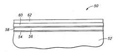
- FIG. 2illustrates a semiconductive wafer fragment 50 at a preliminary processing step of an embodiment of the present invention.
- Wafer fragment 50comprises a substrate 52 , a gate dielectric layer 54 , a polysilicon layer 56 , and a silicide layer 58 .
- Substrate 52 , gate dielectric layer 54 , polysilicon layer 56 and silicide layer 58can comprise materials identical to those utilized in the prior art construction of FIG. 1 for substrate 12 , gate dielectric layer 14 , polysilicon layer 16 and silicide layer 18 , respectively.
- a DARC material layer 60is formed over silicide layer 58 .
- DARC material 60is formed using high density plasma deposition. Such deposition can occur within a reaction chamber.
- a “high density plasma”is defined as a plasma having a density of greater than or equal to 10 10 ions/cm 3 .
- the portion of wafer fragment 50 upon which layer 60 is depositedis preferably maintained at a temperature of from about 300° C. to about 800° C. during the deposition, with about 600° C. one preferred example.
- the temperature of wafer fragment 50can be controlled by flowing helium against a backside of the wafer during the deposition to cool the wafer.
- a denser layer 60can be formed. Such denser layer 60 can be more stable to anneal conditions than a less dense layer 60 .
- a preferred pressure range within a reaction chamber during deposition of layer 60is from about 1 mTorr to 100 mTorr.
- Feed gases utilized in the high density plasma depositioncan comprise SiH 4 , N 2 , O 2 , and argon.
- FIG. 6An exemplary reaction chamber that can be utilized in a method of the present invention is shown schematically in FIG. 6 as part of a reactor 100 .
- Reactor 100comprises coils 102 connected to a power source 104 .
- Coils 102surround a reaction chamber 106 and are configured to generate a plasma within chamber 106 .
- a wafer holder if (chuck) 108is provided within chamber 106 , and holds a semiconductive wafer 110 .
- Wafer holder 108is electrically coupled to a power source 112 .
- power sources 104 and 112can be separate power sources, or can comprise separate feeds originating from a single power source.
- the power from source 104can be, for example, about 2000 watts and can comprise a frequency of about 13.6 megahertz.
- the power to wafer 110 from source 112is preferably biased to less than or equal to about 200 watts and more preferably biased to about 100 watts. In practice, the bias power is typically measured at a chuck 108 holding wafer 110 , rather than at wafer 110 itself.
- An exemplary flow of the feed gases into reaction chamber 106is SiH 4 (100 standard cubic centimeters per minute (sccm)), N 2 (150 sccm), 02 (150 sccm), and argon (200 sccm).
- deposition ratewill exceed the etch rate, so a net effect is deposition of material onto the wafer.
- the rate of depositioncan be calculated by providing no bias at the substrate during deposition, and the etch rate can be calculated by determining an etch rate when no deposition precursors are fed into reactor 106 . Modification of the deposition-to-etch ratio by, for example, adjusting a bias power to substrate 110 , can be utilized to affect the “n” and “k” values of a deposited layer 60 (FIG. 2).
- silicide layer 58is annealed after deposition of DARC material 60 .
- the high pressure plasma deposition of the present inventioncan reduce variability of the optical properties (such as the “n” and “k” values) of material 60 during the anneal of silicide layer 58 .
- variability of “n” and “k” induced by an anneal utilizing the conditions discussed in the “Background” section of this disclosurecan be limited to changes of less than 10%.
- a photoresist layer 62is formed over DARC material 60 .
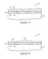
- Photoresist layer 62is then patterned by exposure to a masked light source and a solvent to remove portions of layer 62 and form the resulting structure shown on FIG. 4.
- a patternis then transferred from layer 62 to underlying layers 54 , 56 , 58 and 60 to form a gate stack 70 shown in FIG. 5. It is noted that the application also encompasses embodiments wherein a gate stack encompasses layers 60 , 58 and 56 , and wherein layer 54 is not patterned.
- a method of transferring a pattern from photoresist layer 62 to underlying layers 54 , 56 , 58 and 60is a plasma etch.
- photoresist layer 62can be removed.
- source and drain regionscan be implanted adjacent gate stack 70 and sidewall spacers can be formed along sidewalls of gate stack 70 to form a transistor gate structure from the gate stack.
Landscapes
- Engineering & Computer Science (AREA)
- Physics & Mathematics (AREA)
- General Physics & Mathematics (AREA)
- Condensed Matter Physics & Semiconductors (AREA)
- Manufacturing & Machinery (AREA)
- Computer Hardware Design (AREA)
- Microelectronics & Electronic Packaging (AREA)
- Power Engineering (AREA)
- Architecture (AREA)
- Structural Engineering (AREA)
- Chemical & Material Sciences (AREA)
- Chemical Kinetics & Catalysis (AREA)
- Plasma & Fusion (AREA)
- Electrodes Of Semiconductors (AREA)
- Insulated Gate Type Field-Effect Transistor (AREA)
- Formation Of Insulating Films (AREA)
Abstract
Description
- The invention pertains to methods of forming and utilizing antireflective material layers, and to methods of forming transistor gate stacks.[0001]
- Semiconductor processing frequently involves providing a photoresist layer over a substrate. Portions of the photoresist layer are subsequently exposed to light through a masked light source. The mask contains clear and opaque regions defining a pattern to be created in the photoresist layer. Regions of the photoresist layer which are exposed to light are made either soluble or insoluble in a solvent. If the exposed regions are soluble, a positive image of the mask is produced in the photoresist. The photoresist is therefore termed a positive photoresist. On the other hand, if the non-irradiated regions are dissolved by the solvent, a negative image results. Hence, the photoresist is referred to as a negative photoresist.[0002]
- A difficulty that can occur when exposing photoresist to radiation is that waves of radiation can propagate through the photoresist to a layer beneath the photoresist and then be reflected back up through the photoresist to interact with other waves propagating through the photoresist. The reflected waves can constructively and/or destructively interfere with other waves propagating through the photoresist to create periodic variations of light intensity within the photoresist. Such variations of light intensity can cause the photoresist to receive non-uniform doses of energy throughout its thickness. The non-uniform doses can decrease the accuracy and precision with which a masked pattern is transferred to the photoresist. Accordingly, it is desired to develop methods which suppress radiation waves from being reflected by layers beneath a photoresist layer.[0003]
- A method which has been used with some success to suppress reflected waves is to form an antireflective material beneath a photoresist layer. Antireflective materials are typically materials which absorb radiation and thereby therefore quench reflection of the radiation. Antireflective materials absorb various wavelengths of radiation with varying effectiveness. The number of materials available for use as antireflective materials is limited. Accordingly, it is desired to develop alternative methods of varying the wavelengths absorbed, and effectiveness with which the wavelengths are absorbed, for antireflective materials.[0004]
- A particular type of antireflective coating material is a deposited antireflective coating (DARC). An exemplary DARC is Si[0005]xOyNz, wherein x is from about 40 to about 60, y is from about 29 to about 45, and z is from about 10 to about 16. The DARC can comprise, for example, Si50O37N13. A DARC can be formed by, for example, chemical vapor deposition on a substrate at about 400° C. and under a pressure of from about 4 Torr to about 6.5 Torr, utilizing SiH4and N2O as precursors. The DARC material can be deposited either with or without a plasma being present in a reaction chamber during the deposition. A typical goal in utilizing a DARC film is to reduce reflected radiation reaching an overlying layer of photoresist to less than 10% of incident radiation at the DARC film.
- A prior art process utilizing a DARC material is described with reference to a[0006]
semiconductive wafer fragment 10 in FIG. 1. Waferfragment 10 comprises asubstrate 12.Substrate 12 can comprise, for example, monocrystalline silicon lightly doped with a background p-type dopant. To aid in interpretation of the claims that follow, the term “semiconductive substrate” is defined to mean any construction comprising semiconductive material, including, but not limited to, bulk semiconductive materials such as a semiconductive wafer (either alone or in assemblies comprising other materials thereon), and semiconductive material layers (either alone or in assemblies comprising other materials). The term “substrates” refers to any supporting structure, including, but not limited to, the semiconductive substrates described above. - A gate[0007]
dielectric layer 14,polysilicon layer 16, andsilicide layer 18 are formed oversubstrate 12. Gatedielectric layer 14 can comprise, for example, silicon dioxide;polysilicon layer 16 can comprise, for example, conductively doped polysilicon; andsilicide layer 18 can comprise, for example, tungsten silicide or titanium silicide.Layers - An[0008]
antireflective coating layer 20 is provided oversilicide layer 18, and aphotoresist layer 22 is provided overantireflective coating layer 20.Antireflective coating layer 20 can comprise, for example, an inorganic layer such as SixOyNz. In practice the layer can be substantially inorganic, with the term “substantially inorganic” indicating that the layer can contain a small amount of carbon (less than 1%). - [0009]
Silicide layer 18 is preferably subjected to an anneal to improve a crystalline structure and a conductivity of the silicide layer prior to utilization of the layer in a transistor gate. The anneal ofsilicide layer 18 can comprise, for example, a temperature of 850° C. and a pressure of 1 atmosphere for a time of 30 minutes. - [0010]
DARC material 20 is typically provided oversilicide layer 18 prior to the anneal to protectlayer 18 from gaseous oxygen during the anneal. If gaseous oxygen interacts withlayer 18 during the anneal, the oxygen can oxidize a portion oflayer 18 and adversely effect conductivity oflayer 18. Unfortunately, the anneal conditions can detrimentally influence optical properties ofDARC material 20. Specifically,DARC material 20 has optical properties that can be described by a refractive index coefficient (n) and an extinction coefficient (energy absorption coefficient) (k). The anneal conditions which improve conductivity ofsilicide layer 18 can alter one or both of “n” and “k” oflayer 20. A stoichiometry of the materials oflayer 20 is typically carefully chosen to adjust “n” and “k” of the material to appropriate parameters which will substantially quench reflected radiation before the radiation reachesphotoresist layer 22. The effect of the anneal conditions on “n” and “k” can push such parameters out of an optimum adjusted range. Accordingly, it is desired to develop methods of forming DARC materials wherein “n” and “k” of the materials will be resistant to anneal condition induced changes. - In one aspect, the invention encompasses a semiconductor processing method wherein silicon, nitrogen and oxygen in gaseous form are exposed to a high density plasma during deposition of a silicon, nitrogen and oxygen containing solid layer over a substrate.[0011]
- In another aspect, the invention encompasses a semiconductor processing method of photolithographic processing. A metal silicide layer is formed over a substrate. An antireflective material layer is deposited over the metal silicide utilizing a high density plasma. A layer of photoresist is formed over the antireflective material layer. The layer of photoresist is photolithographically patterned.[0012]
- In yet another aspect, the invention encompasses a transistor gate stack forming method. A polysilicon layer is formed over a substrate. A metal silicide layer is formed over the polysilicon layer. An is antireflective material layer is deposited over the metal silicide utilizing a high density plasma. A layer of photoresist is formed over the antireflective material layer. The layer of photoresist is photolithographically patterned to form a patterned masking layer from the layer of photoresist. A pattern is transferred from the patterned masking layer to the antireflective material layer, metal silicide layer and polysilicon layer to pattern the antireflective material layer, metal silicide layer and polysilicon layer into a transistor gate stack.[0013]
- Preferred embodiments of the invention are described below with reference to the following accompanying drawings.[0014]
- FIG. 1 is a fragmentary, diagramatic, cross-sectional view of a prior art semiconductive wafer fragment.[0015]
- FIG. 2 is a fragmentary, diagrammatic, cross-sectional view of a semiconductive wafer fragment at a preliminary processing step of a method of the present invention.[0016]
- FIG. 3 is a view of the FIG. 2 wafer fragment at a processing step subsequent to that of FIG. 2.[0017]
- FIG. 4 is a view of the FIG. 2 wafer fragment at a processing step subsequent to that of FIG. 3.[0018]
- FIG. 5 is a view of the FIG. 2 wafer fragment at a processing step subsequent to that of FIG. 4.[0019]
- FIG. 6 is a diagrammatic, cross-sectional, schematic view of a reaction chamber which can be utilized in methods of the present invention.[0020]
- This disclosure of the invention is submitted in furtherance of the constitutional purposes of the U.S. Patent Laws “to promote the progress of science and useful arts” (Article 1, Section 8).[0021]
- FIG. 2 illustrates a[0022]
semiconductive wafer fragment 50 at a preliminary processing step of an embodiment of the present invention.Wafer fragment 50 comprises asubstrate 52, agate dielectric layer 54, apolysilicon layer 56, and asilicide layer 58.Substrate 52,gate dielectric layer 54,polysilicon layer 56 andsilicide layer 58 can comprise materials identical to those utilized in the prior art construction of FIG. 1 forsubstrate 12,gate dielectric layer 14,polysilicon layer 16 andsilicide layer 18, respectively. - A[0023]
DARC material layer 60 is formed oversilicide layer 58. In contrast to prior art methods,DARC material 60 is formed using high density plasma deposition. Such deposition can occur within a reaction chamber. To aid in interpretation of the claims that follow, a “high density plasma” is defined as a plasma having a density of greater than or equal to 1010ions/cm3. The portion ofwafer fragment 50 upon whichlayer 60 is deposited is preferably maintained at a temperature of from about 300° C. to about 800° C. during the deposition, with about 600° C. one preferred example. The temperature ofwafer fragment 50 can be controlled by flowing helium against a backside of the wafer during the deposition to cool the wafer. At higher temperatures adenser layer 60 can be formed. Suchdenser layer 60 can be more stable to anneal conditions than a lessdense layer 60. A preferred pressure range within a reaction chamber during deposition oflayer 60 is from about 1 mTorr to 100 mTorr. Feed gases utilized in the high density plasma deposition can comprise SiH4, N2, O2, and argon. - An exemplary reaction chamber that can be utilized in a method of the present invention is shown schematically in FIG. 6 as part of a[0024]
reactor 100.Reactor 100 comprisescoils 102 connected to apower source 104.Coils 102 surround areaction chamber 106 and are configured to generate a plasma withinchamber 106. A wafer holder if (chuck)108 is provided withinchamber 106, and holds asemiconductive wafer 110.Wafer holder 108 is electrically coupled to apower source 112. It is noted thatpower sources source 104 can be, for example, about 2000 watts and can comprise a frequency of about 13.6 megahertz. The power towafer 110 fromsource 112 is preferably biased to less than or equal to about 200 watts and more preferably biased to about 100 watts. In practice, the bias power is typically measured at achuck 108 holdingwafer 110, rather than atwafer 110 itself. - An exemplary flow of the feed gases into[0025]
reaction chamber 106 is SiH4(100 standard cubic centimeters per minute (sccm)), N2(150 sccm), 02 (150 sccm), and argon (200 sccm). - During deposition of layer[0026]60 (FIG. 2) onto a semiconductive wafer in a high pressure plasma process of the present invention, there will likely be both deposition and etch processes occurring simultaneously, resulting in a deposition-to-etch ratio. The deposition rate will exceed the etch rate, so a net effect is deposition of material onto the wafer. The rate of deposition can be calculated by providing no bias at the substrate during deposition, and the etch rate can be calculated by determining an etch rate when no deposition precursors are fed into
reactor 106. Modification of the deposition-to-etch ratio by, for example, adjusting a bias power tosubstrate 110, can be utilized to affect the “n” and “k” values of a deposited layer60 (FIG. 2). - Referring again to FIG. 2,[0027]
silicide layer 58 is annealed after deposition ofDARC material 60. The high pressure plasma deposition of the present invention can reduce variability of the optical properties (such as the “n” and “k” values) ofmaterial 60 during the anneal ofsilicide layer 58. For instance the variability of “n” and “k” induced by an anneal utilizing the conditions discussed in the “Background” section of this disclosure can be limited to changes of less than 10%. - Referring to FIG. 3, a[0028]
photoresist layer 62 is formed overDARC material 60.Photoresist layer 62 is then patterned by exposure to a masked light source and a solvent to remove portions oflayer 62 and form the resulting structure shown on FIG. 4. - A pattern is then transferred from[0029]
layer 62 tounderlying layers gate stack 70 shown in FIG. 5. It is noted that the application also encompasses embodiments wherein a gate stack encompasseslayers layer 54 is not patterned. A method of transferring a pattern fromphotoresist layer 62 tounderlying layers gate stack 70,photoresist layer 62 can be removed. Also, source and drain regions can be implantedadjacent gate stack 70 and sidewall spacers can be formed along sidewalls ofgate stack 70 to form a transistor gate structure from the gate stack. - In compliance with the statute, the invention has been described in language more or less specific as to structural and methodical features. It is to be understood, however, that the invention is not limited to the specific features shown and described, since the means herein disclosed comprise preferred forms of putting the invention into effect. The invention is, therefore, claimed in any of its forms or modifications within the proper scope of the appended claims appropriately interpreted in accordance with the doctrine of equivalents.[0030]
Claims (28)
Priority Applications (1)
| Application Number | Priority Date | Filing Date | Title |
|---|---|---|---|
| US10/805,557US7151054B2 (en) | 1998-09-03 | 2004-03-19 | Semiconductor processing methods of forming and utilizing antireflective material layers, and methods of forming transistor gate stacks |
Applications Claiming Priority (3)
| Application Number | Priority Date | Filing Date | Title |
|---|---|---|---|
| US09/146,841US6268282B1 (en) | 1998-09-03 | 1998-09-03 | Semiconductor processing methods of forming and utilizing antireflective material layers, and methods of forming transistor gate stacks |
| US09/891,570US6727173B2 (en) | 1998-09-03 | 2001-06-25 | Semiconductor processing methods of forming an utilizing antireflective material layers, and methods of forming transistor gate stacks |
| US10/805,557US7151054B2 (en) | 1998-09-03 | 2004-03-19 | Semiconductor processing methods of forming and utilizing antireflective material layers, and methods of forming transistor gate stacks |
Related Parent Applications (1)
| Application Number | Title | Priority Date | Filing Date |
|---|---|---|---|
| US09/891,570ContinuationUS6727173B2 (en) | 1998-09-03 | 2001-06-25 | Semiconductor processing methods of forming an utilizing antireflective material layers, and methods of forming transistor gate stacks |
Publications (2)
| Publication Number | Publication Date |
|---|---|
| US20040180537A1true US20040180537A1 (en) | 2004-09-16 |
| US7151054B2 US7151054B2 (en) | 2006-12-19 |
Family
ID=22519203
Family Applications (3)
| Application Number | Title | Priority Date | Filing Date |
|---|---|---|---|
| US09/146,841Expired - LifetimeUS6268282B1 (en) | 1998-09-03 | 1998-09-03 | Semiconductor processing methods of forming and utilizing antireflective material layers, and methods of forming transistor gate stacks |
| US09/891,570Expired - LifetimeUS6727173B2 (en) | 1998-09-03 | 2001-06-25 | Semiconductor processing methods of forming an utilizing antireflective material layers, and methods of forming transistor gate stacks |
| US10/805,557Expired - Fee RelatedUS7151054B2 (en) | 1998-09-03 | 2004-03-19 | Semiconductor processing methods of forming and utilizing antireflective material layers, and methods of forming transistor gate stacks |
Family Applications Before (2)
| Application Number | Title | Priority Date | Filing Date |
|---|---|---|---|
| US09/146,841Expired - LifetimeUS6268282B1 (en) | 1998-09-03 | 1998-09-03 | Semiconductor processing methods of forming and utilizing antireflective material layers, and methods of forming transistor gate stacks |
| US09/891,570Expired - LifetimeUS6727173B2 (en) | 1998-09-03 | 2001-06-25 | Semiconductor processing methods of forming an utilizing antireflective material layers, and methods of forming transistor gate stacks |
Country Status (5)
| Country | Link |
|---|---|
| US (3) | US6268282B1 (en) |
| JP (1) | JP3542118B2 (en) |
| KR (1) | KR100423560B1 (en) |
| AU (1) | AU5590799A (en) |
| WO (1) | WO2000014781A1 (en) |
Families Citing this family (24)
| Publication number | Priority date | Publication date | Assignee | Title |
|---|---|---|---|---|
| US6800378B2 (en)* | 1998-02-19 | 2004-10-05 | 3M Innovative Properties Company | Antireflection films for use with displays |
| US7804115B2 (en) | 1998-02-25 | 2010-09-28 | Micron Technology, Inc. | Semiconductor constructions having antireflective portions |
| US6274292B1 (en) | 1998-02-25 | 2001-08-14 | Micron Technology, Inc. | Semiconductor processing methods |
| US6281100B1 (en) | 1998-09-03 | 2001-08-28 | Micron Technology, Inc. | Semiconductor processing methods |
| US6268282B1 (en)* | 1998-09-03 | 2001-07-31 | Micron Technology, Inc. | Semiconductor processing methods of forming and utilizing antireflective material layers, and methods of forming transistor gate stacks |
| US6828683B2 (en)* | 1998-12-23 | 2004-12-07 | Micron Technology, Inc. | Semiconductor devices, and semiconductor processing methods |
| US7235499B1 (en) | 1999-01-20 | 2007-06-26 | Micron Technology, Inc. | Semiconductor processing methods |
| US6291361B1 (en)* | 1999-03-24 | 2001-09-18 | Conexant Systems, Inc. | Method and apparatus for high-resolution in-situ plasma etching of inorganic and metal films |
| US7067414B1 (en) | 1999-09-01 | 2006-06-27 | Micron Technology, Inc. | Low k interlevel dielectric layer fabrication methods |
| US6440860B1 (en)* | 2000-01-18 | 2002-08-27 | Micron Technology, Inc. | Semiconductor processing methods of transferring patterns from patterned photoresists to materials, and structures comprising silicon nitride |
| US7132219B2 (en)* | 2001-02-02 | 2006-11-07 | Brewer Science Inc. | Polymeric antireflective coatings deposited by plasma enhanced chemical vapor deposition |
| US6573175B1 (en)* | 2001-11-30 | 2003-06-03 | Micron Technology, Inc. | Dry low k film application for interlevel dielectric and method of cleaning etched features |
| US6852474B2 (en)* | 2002-04-30 | 2005-02-08 | Brewer Science Inc. | Polymeric antireflective coatings deposited by plasma enhanced chemical vapor deposition |
| KR100457844B1 (en)* | 2002-08-27 | 2004-11-18 | 삼성전자주식회사 | Method Of Etching Semiconductor Device |
| US6853043B2 (en)* | 2002-11-04 | 2005-02-08 | Applied Materials, Inc. | Nitrogen-free antireflective coating for use with photolithographic patterning |
| US20070207406A1 (en)* | 2004-04-29 | 2007-09-06 | Guerrero Douglas J | Anti-reflective coatings using vinyl ether crosslinkers |
| US20050255410A1 (en) | 2004-04-29 | 2005-11-17 | Guerrero Douglas J | Anti-reflective coatings using vinyl ether crosslinkers |
| KR100591133B1 (en) | 2004-12-15 | 2006-06-19 | 동부일렉트로닉스 주식회사 | Gate pattern forming method using argon fluoride photoresist |
| US7914974B2 (en) | 2006-08-18 | 2011-03-29 | Brewer Science Inc. | Anti-reflective imaging layer for multiple patterning process |
| JP4462273B2 (en)* | 2007-01-23 | 2010-05-12 | セイコーエプソン株式会社 | Optical article and manufacturing method thereof |
| US8283258B2 (en)* | 2007-08-16 | 2012-10-09 | Micron Technology, Inc. | Selective wet etching of hafnium aluminum oxide films |
| JP5357186B2 (en)* | 2008-01-29 | 2013-12-04 | ブルーワー サイエンス アイ エヌ シー. | On-track process for hard mask pattern formation by multiple dark field exposure |
| US9640396B2 (en) | 2009-01-07 | 2017-05-02 | Brewer Science Inc. | Spin-on spacer materials for double- and triple-patterning lithography |
| EP3692408A1 (en) | 2017-10-05 | 2020-08-12 | Signify Holding B.V. | Luminaire and lighting method |
Citations (98)
| Publication number | Priority date | Publication date | Assignee | Title |
|---|---|---|---|---|
| US4158717A (en)* | 1977-02-14 | 1979-06-19 | Varian Associates, Inc. | Silicon nitride film and method of deposition |
| US4474975A (en)* | 1983-05-09 | 1984-10-02 | The United States Of America As Represented By The Administrator Of The National Aeronautics And Space Administration | Process for producing tris (N-methylamino) methylsilane |
| US4523214A (en)* | 1981-07-03 | 1985-06-11 | Fuji Photo Film Co., Ltd. | Solid state image pickup device utilizing microcrystalline and amorphous silicon |
| US4592129A (en)* | 1985-04-01 | 1986-06-03 | Motorola, Inc. | Method of making an integral, multiple layer antireflection coating by hydrogen ion implantation |
| US4600671A (en)* | 1983-09-12 | 1986-07-15 | Canon Kabushiki Kaisha | Photoconductive member having light receiving layer of A-(Si-Ge) and N |
| US4648904A (en)* | 1986-02-14 | 1987-03-10 | Scm Corporation | Aqueous systems containing silanes for rendering masonry surfaces water repellant |
| US4695859A (en)* | 1986-10-20 | 1987-09-22 | Energy Conversion Devices, Inc. | Thin film light emitting diode, photonic circuit employing said diode imager employing said circuits |
| US4702936A (en)* | 1984-09-20 | 1987-10-27 | Applied Materials Japan, Inc. | Gas-phase growth process |
| US4805683A (en)* | 1988-03-04 | 1989-02-21 | International Business Machines Corporation | Method for producing a plurality of layers of metallurgy |
| US4833096A (en)* | 1988-01-19 | 1989-05-23 | Atmel Corporation | EEPROM fabrication process |
| US4863755A (en)* | 1987-10-16 | 1989-09-05 | The Regents Of The University Of California | Plasma enhanced chemical vapor deposition of thin films of silicon nitride from cyclic organosilicon nitrogen precursors |
| US4971655A (en)* | 1989-12-26 | 1990-11-20 | Micron Technology, Inc. | Protection of a refractory metal silicide during high-temperature processing using a dual-layer cap of silicon dioxide and silicon nitride |
| US4992306A (en)* | 1990-02-01 | 1991-02-12 | Air Products Abd Chemicals, Inc. | Deposition of silicon dioxide and silicon oxynitride films using azidosilane sources |
| US5036383A (en)* | 1989-04-27 | 1991-07-30 | Kabushiki Kaisha Toshiba | Semiconductor device having an improved bonding pad |
| US5061509A (en)* | 1989-08-25 | 1991-10-29 | Kabushiki Kaisha Toshiba | Method of manufacturing polyimide thin film and method of manufacturing liquid crystal orientation film of polyimide |
| US5219613A (en)* | 1990-06-13 | 1993-06-15 | Wacker-Chemitronic Gesellschaft Fur Elektronik-Grundstoffe Mbh | Process for producing storage-stable surfaces of polished silicon wafers |
| US5234869A (en)* | 1990-06-28 | 1993-08-10 | Kabushiki Kaisha Toshiba | Method of manufacturing silicon nitride film |
| US5260600A (en)* | 1990-06-05 | 1993-11-09 | Mitsubishi Denki Kabushiki Kaisha | Semiconductor device having protective insulating film |
| US5276347A (en)* | 1991-12-18 | 1994-01-04 | Sgs-Thomson Microelectronics, Inc. | Gate overlapping LDD structure |
| US5302366A (en)* | 1991-03-28 | 1994-04-12 | Phillips Petroleum Company | Production of silicon product containing both carbon and nitrogen |
| US5356515A (en)* | 1990-10-19 | 1994-10-18 | Tokyo Electron Limited | Dry etching method |
| US5405489A (en)* | 1991-10-30 | 1995-04-11 | Samsung Electronics Co., Ltd. | Method for fabricating an interlayer-dielectric film of a semiconductor device by using a plasma treatment prior to reflow |
| US5461003A (en)* | 1994-05-27 | 1995-10-24 | Texas Instruments Incorporated | Multilevel interconnect structure with air gaps formed between metal leads |
| US5470772A (en)* | 1991-11-06 | 1995-11-28 | Intel Corporation | Silicidation method for contactless EPROM related devices |
| US5498555A (en)* | 1994-11-07 | 1996-03-12 | United Microelectronics Corporation | Method of making LDD with polysilicon and dielectric spacers |
| US5536857A (en)* | 1994-07-05 | 1996-07-16 | Ford Motor Company | Single source volatile precursor for SiO2.TiO2 powders and films |
| US5541445A (en)* | 1991-08-14 | 1996-07-30 | Mitel Corporation | High performance passivation for semiconductor devices |
| US5554567A (en)* | 1994-09-01 | 1996-09-10 | Taiwan Semiconductor Manufacturing Company Ltd. | Method for improving adhesion to a spin-on-glass |
| US5591494A (en)* | 1993-09-24 | 1997-01-07 | Applied Materials, Inc. | Deposition of silicon nitrides by plasma-enhanced chemical vapor deposition |
| US5593741A (en)* | 1992-11-30 | 1997-01-14 | Nec Corporation | Method and apparatus for forming silicon oxide film by chemical vapor deposition |
| US5639687A (en)* | 1993-07-06 | 1997-06-17 | Motorola Inc. | Method for forming an integrated circuit pattern on a semiconductor substrate using silicon-rich silicon nitride |
| US5652187A (en)* | 1991-10-30 | 1997-07-29 | Samsung Electronics Co., Ltd. | Method for fabricating doped interlayer-dielectric film of semiconductor device using a plasma treatment |
| US5656337A (en)* | 1993-08-31 | 1997-08-12 | Samsung Electronics Co., Ltd. | Method of forming a dielectric layer |
| US5661093A (en)* | 1996-09-12 | 1997-08-26 | Applied Materials, Inc. | Method for the stabilization of halogen-doped films through the use of multiple sealing layers |
| US5667015A (en)* | 1995-02-03 | 1997-09-16 | Bj Services Company | Well barrier |
| US5677015A (en)* | 1994-03-17 | 1997-10-14 | Sony Corporation | High dielectric constant material containing tantalum, process for forming high dielectric constant film containing tantalum, and semiconductor device using the same |
| US5709741A (en)* | 1995-02-28 | 1998-01-20 | Dow Corning Toray Silicone Co., Ltd. | Water repellent for application to glass and water-repellent glass |
| US5711987A (en)* | 1996-10-04 | 1998-01-27 | Dow Corning Corporation | Electronic coatings |
| US5731242A (en)* | 1993-10-15 | 1998-03-24 | Intel Corporation | Self-aligned contact process in semiconductor fabrication |
| US5744399A (en)* | 1995-11-13 | 1998-04-28 | Lsi Logic Corporation | Process for forming low dielectric constant layers using fullerenes |
| US5747388A (en)* | 1992-09-18 | 1998-05-05 | Siemens Aktiengesellschaft | Antireflection layer and process for lithographically structuring a layer |
| US5753320A (en)* | 1985-09-26 | 1998-05-19 | Canon Kabushiki Kaisha | Process for forming deposited film |
| US5759746A (en)* | 1996-05-24 | 1998-06-02 | Kabushiki Kaisha Toshiba | Fabrication process using a thin resist |
| US5783493A (en)* | 1997-01-27 | 1998-07-21 | Taiwan Semiconductor Manufacturing Company Ltd. | Method for reducing precipitate defects using a plasma treatment post BPSG etchback |
| US5796151A (en)* | 1996-12-19 | 1998-08-18 | Texas Instruments Incorporated | Semiconductor stack having a dielectric sidewall for prevention of oxidation of tungsten in tungsten capped poly-silicon gate electrodes |
| US5800877A (en)* | 1995-08-18 | 1998-09-01 | Canon Sales Co., Inc. | Method for forming a fluorine containing silicon oxide film |
| US5807660A (en)* | 1997-02-03 | 1998-09-15 | Taiwan Semiconductor Manufacturing Company Ltd. | Avoid photoresist lifting by post-oxide-dep plasma treatment |
| US5840610A (en)* | 1997-01-16 | 1998-11-24 | Advanced Micro Devices, Inc. | Enhanced oxynitride gate dielectrics using NF3 gas |
| US5858880A (en)* | 1994-05-14 | 1999-01-12 | Trikon Equipment Limited | Method of treating a semi-conductor wafer |
| US5874367A (en)* | 1992-07-04 | 1999-02-23 | Trikon Technologies Limited | Method of treating a semi-conductor wafer |
| US5883014A (en)* | 1997-06-03 | 1999-03-16 | United Microelectronics Corp. | Method for treating via sidewalls with hydrogen plasma |
| US5948482A (en)* | 1995-09-19 | 1999-09-07 | University Of New Mexico | Ambient pressure process for preparing aerogel thin films reliquified sols useful in preparing aerogel thin films |
| US5962581A (en)* | 1995-04-28 | 1999-10-05 | Kabushiki Kaisha Toshiba | Silicone polymer composition, method of forming a pattern and method of forming an insulating film |
| US5968611A (en)* | 1997-11-26 | 1999-10-19 | The Research Foundation Of State University Of New York | Silicon nitrogen-based films and method of making the same |
| US5985519A (en)* | 1997-03-19 | 1999-11-16 | Fujitsu Limited | Method of manufacturing semiconductor device using top antireflection film |
| US6017614A (en)* | 1997-07-14 | 2000-01-25 | Vanguard International Semiconductor Corporation | Plasma-enhanced chemical vapor deposited SIO2 /SI3 N4 multilayer passivation layer for semiconductor applications |
| US6022404A (en)* | 1995-01-12 | 2000-02-08 | Degussa Aktiengesellschaft | Surface-modified, pyrogenically produced mixed oxides, method of their production and use |
| US6028015A (en)* | 1999-03-29 | 2000-02-22 | Lsi Logic Corporation | Process for treating damaged surfaces of low dielectric constant organo silicon oxide insulation material to inhibit moisture absorption |
| US6030901A (en)* | 1999-06-24 | 2000-02-29 | Advanced Micro Devices, Inc. | Photoresist stripping without degrading low dielectric constant materials |
| US6037228A (en)* | 1999-02-12 | 2000-03-14 | United Microelectronics Corp. | Method of fabricating self-aligned contact window which includes forming a undoped polysilicon spacer that extends into a recess of the gate structure |
| US6054379A (en)* | 1998-02-11 | 2000-04-25 | Applied Materials, Inc. | Method of depositing a low k dielectric with organo silane |
| US6057217A (en)* | 1996-07-25 | 2000-05-02 | Nec Corporation | Process for production of semiconductor device with foreign element introduced into silicon dioxide film |
| US6114736A (en)* | 1996-10-29 | 2000-09-05 | International Business Machines Corporation | Controlled dopant diffusion and metal contamination in thin polycide gate conductor of MOSFET device |
| US6118163A (en)* | 1998-02-04 | 2000-09-12 | Advanced Micro Devices, Inc. | Transistor with integrated poly/metal gate electrode |
| US6121133A (en)* | 1997-08-22 | 2000-09-19 | Micron Technology, Inc. | Isolation using an antireflective coating |
| US6124641A (en)* | 1997-06-26 | 2000-09-26 | Mitsubishi Denki Kabushiki Kaisha | Semiconductor device organic insulator film |
| US6133618A (en)* | 1997-08-14 | 2000-10-17 | Lucent Technologies Inc. | Semiconductor device having an anti-reflective layer and a method of manufacture thereof |
| US6200863B1 (en)* | 1999-03-24 | 2001-03-13 | Advanced Micro Devices, Inc. | Process for fabricating a semiconductor device having assymetric source-drain extension regions |
| US6208004B1 (en)* | 1998-08-19 | 2001-03-27 | Philips Semiconductor, Inc. | Semiconductor device with high-temperature-stable gate electrode for sub-micron applications and fabrication thereof |
| US6218292B1 (en)* | 1997-12-18 | 2001-04-17 | Advanced Micro Devices, Inc. | Dual layer bottom anti-reflective coating |
| US6268282B1 (en)* | 1998-09-03 | 2001-07-31 | Micron Technology, Inc. | Semiconductor processing methods of forming and utilizing antireflective material layers, and methods of forming transistor gate stacks |
| US6284677B1 (en)* | 1997-04-18 | 2001-09-04 | United Semiconductor Corp. | Method of forming fluorosilicate glass (FSG) layers with moisture-resistant capability |
| US20020016085A1 (en)* | 2000-07-14 | 2002-02-07 | Kegang Huang | Method and apparatus for treating low k dielectric layers to reduce diffusion |
| US6348407B1 (en)* | 2001-03-15 | 2002-02-19 | Chartered Semiconductor Manufacturing Inc. | Method to improve adhesion of organic dielectrics in dual damascene interconnects |
| US20020098684A1 (en)* | 1999-09-01 | 2002-07-25 | Weimin Li | Low k interlevel dielectric layer fabrication methods |
| US6429115B1 (en)* | 2001-02-27 | 2002-08-06 | United Microelectronics Corp. | Method of manufacturing multilevel interconnects including performing a surface treatment to form a hydrophilic surface layer |
| US6432791B1 (en)* | 1999-04-14 | 2002-08-13 | Texas Instruments Incorporated | Integrated circuit capacitor and method |
| US6435943B1 (en)* | 2000-10-26 | 2002-08-20 | United Microelectronics Corp. | Method of chemical mechanical polishing organic silicon material with low dielectric constant |
| US6436808B1 (en)* | 2000-12-07 | 2002-08-20 | Advanced Micro Devices, Inc. | NH3/N2-plasma treatment to prevent organic ILD degradation |
| US6444593B1 (en)* | 1998-12-02 | 2002-09-03 | Advanced Micro Devices, Inc. | Surface treatment of low-K SiOF to prevent metal interaction |
| US6465372B1 (en)* | 1999-08-17 | 2002-10-15 | Applied Materials, Inc. | Surface treatment of C-doped SiO2 film to enhance film stability during O2 ashing |
| US6503818B1 (en)* | 1999-04-02 | 2003-01-07 | Taiwan Semiconductor Manufacturing Company | Delamination resistant multi-layer composite dielectric layer employing low dielectric constant dielectric material |
| US20030077916A1 (en)* | 2001-10-11 | 2003-04-24 | Applied Materials, Inc. | Method of eliminating photoresist poisoning in damascene applications |
| US20030164354A1 (en)* | 1999-12-28 | 2003-09-04 | Applied Materials, Inc. | System level in-situ integrated dielectric etch process particularly useful for copper dual damascene |
| US20030173671A1 (en)* | 2002-03-13 | 2003-09-18 | Nec Corporation | Semiconductor device and manufacturing method for the same |
| US6627535B2 (en)* | 2000-01-19 | 2003-09-30 | Trikon Holdings Ltd. | Methods and apparatus for forming a film on a substrate |
| US6632712B1 (en)* | 2002-10-03 | 2003-10-14 | Chartered Semiconductor Manufacturing Ltd. | Method of fabricating variable length vertical transistors |
| US6638875B2 (en)* | 1999-08-05 | 2003-10-28 | Axcelis Technologies, Inc. | Oxygen free plasma stripping process |
| US20030201465A1 (en)* | 2002-04-18 | 2003-10-30 | Daisuke Ryuzaki | Semiconductor manufacturing method for low-k insulating film |
| US6720247B2 (en)* | 2000-12-14 | 2004-04-13 | Texas Instruments Incorporated | Pre-pattern surface modification for low-k dielectrics using A H2 plasma |
| US20040071878A1 (en)* | 2002-08-15 | 2004-04-15 | Interuniversitair Microelektronica Centrum (Imec Vzw) | Surface preparation using plasma for ALD Films |
| US6723631B2 (en)* | 2000-09-29 | 2004-04-20 | Renesas Technology Corporation | Fabrication method of semiconductor integrated circuit device |
| US20040126671A1 (en)* | 2002-12-31 | 2004-07-01 | Steven Smith | Structure and process for a pellicle membrane for 157 nanometer lithography |
| US20040175933A1 (en)* | 2003-03-05 | 2004-09-09 | Sanyo Electric Co., Ltd. | Method of forming wiring structure |
| US6790778B1 (en)* | 2003-09-10 | 2004-09-14 | Taiwan Semiconductor Manufacturing Co., Ltd. | Method for capping over a copper layer |
| US20050023691A1 (en)* | 2003-07-31 | 2005-02-03 | Kei Watanabe | Semiconductor device and manufacturing method thereof |
| US20050064698A1 (en)* | 2003-09-19 | 2005-03-24 | Hui-Lin Chang | Two step post-deposition treatment of ILD layer for a lower dielectric constant and improved mechanical properties |
| US20050191828A1 (en)* | 2000-08-11 | 2005-09-01 | Applied Materials, Inc. | Method for ion implanting insulator material to reduce dielectric constant |
Family Cites Families (123)
| Publication number | Priority date | Publication date | Assignee | Title |
|---|---|---|---|---|
| US2553314A (en) | 1944-07-01 | 1951-05-15 | Gen Electric | Method of rendering materials water repellent |
| US4562091A (en) | 1982-12-23 | 1985-12-31 | International Business Machines Corporation | Use of plasma polymerized orgaosilicon films in fabrication of lift-off masks |
| US4444617A (en) | 1983-01-06 | 1984-04-24 | Rockwell International Corporation | Reactive ion etching of molybdenum silicide and N+ polysilicon |
| US4552783A (en) | 1984-11-05 | 1985-11-12 | General Electric Company | Enhancing the selectivity of tungsten deposition on conductor and semiconductor surfaces |
| US6087267A (en) | 1986-03-04 | 2000-07-11 | Motorola, Inc. | Process for forming an integrated circuit |
| US4764247A (en) | 1987-03-18 | 1988-08-16 | Syn Labs, Inc. | Silicon containing resists |
| JPH043699Y2 (en) | 1987-03-30 | 1992-02-05 | ||
| JPS63316476A (en) | 1987-06-18 | 1988-12-23 | Seiko Instr & Electronics Ltd | Semiconductor device and manufacture thereof |
| US4755478A (en) | 1987-08-13 | 1988-07-05 | International Business Machines Corporation | Method of forming metal-strapped polysilicon gate electrode for FET device |
| US4870470A (en) | 1987-10-16 | 1989-09-26 | International Business Machines Corporation | Non-volatile memory cell having Si rich silicon nitride charge trapping layer |
| US4940509A (en) | 1988-03-25 | 1990-07-10 | Texas Instruments, Incorporated | Isotropic etchant for capped silicide processes |
| US5270267A (en) | 1989-05-31 | 1993-12-14 | Mitel Corporation | Curing and passivation of spin on glasses by a plasma process wherein an external polarization field is applied to the substrate |
| US4910160A (en) | 1989-06-06 | 1990-03-20 | National Semiconductor Corporation | High voltage complementary NPN/PNP process |
| US5244537A (en) | 1989-12-27 | 1993-09-14 | Honeywell, Inc. | Fabrication of an electronic microvalve apparatus |
| US5140390A (en) | 1990-02-16 | 1992-08-18 | Hughes Aircraft Company | High speed silicon-on-insulator device |
| US5034348A (en) | 1990-08-16 | 1991-07-23 | International Business Machines Corp. | Process for forming refractory metal silicide layers of different thicknesses in an integrated circuit |
| WO1992012535A1 (en) | 1991-01-08 | 1992-07-23 | Fujitsu Limited | Process for forming silicon oxide film |
| US5677111A (en) | 1991-12-20 | 1997-10-14 | Sony Corporation | Process for production of micropattern utilizing antireflection film |
| US5472829A (en) | 1991-12-30 | 1995-12-05 | Sony Corporation | Method of forming a resist pattern by using an anti-reflective layer |
| US5472827A (en) | 1991-12-30 | 1995-12-05 | Sony Corporation | Method of forming a resist pattern using an anti-reflective layer |
| US5670297A (en) | 1991-12-30 | 1997-09-23 | Sony Corporation | Process for the formation of a metal pattern |
| JPH0667019A (en) | 1992-01-17 | 1994-03-11 | Asahi Glass Co Ltd | Antireflection layer and its production |
| US5543654A (en) | 1992-01-28 | 1996-08-06 | Thunderbird Technologies, Inc. | Contoured-tub fermi-threshold field effect transistor and method of forming same |
| JPH05263255A (en) | 1992-03-19 | 1993-10-12 | Hitachi Electron Eng Co Ltd | Plasma cvd device |
| JPH05275345A (en) | 1992-03-30 | 1993-10-22 | Nippon Sheet Glass Co Ltd | Plasma cvd method and its device |
| EP0572704B1 (en) | 1992-06-05 | 2000-04-19 | Semiconductor Process Laboratory Co., Ltd. | Method for manufacturing a semiconductor device including method of reforming an insulating film formed by low temperature CVD |
| TW363146B (en) | 1992-08-20 | 1999-07-01 | Sony Corp | An anti-reflective layer and a method of forming a photoresist pattern |
| US5286661A (en) | 1992-08-26 | 1994-02-15 | Motorola, Inc. | Method of forming a bipolar transistor having an emitter overhang |
| US5429987A (en) | 1993-01-25 | 1995-07-04 | Sharp Microelectronics Technology, Inc. | Method for profile control of selective metallization |
| JPH06244172A (en) | 1993-02-18 | 1994-09-02 | Toray Ind Inc | Multilayered wiring structure |
| US5312768A (en) | 1993-03-09 | 1994-05-17 | Micron Technology, Inc. | Integrated process for fabricating raised, source/drain, short-channel transistors |
| US5397684A (en) | 1993-04-27 | 1995-03-14 | International Business Machines Corporation | Antireflective polyimide dielectric for photolithography |
| KR970004447B1 (en) | 1993-09-08 | 1997-03-27 | 삼성전자 주식회사 | A method for forming anti-reflect-film and its application to manufacturing semiconductor devices |
| US5508881A (en) | 1994-02-01 | 1996-04-16 | Quality Microcircuits Corporation | Capacitors and interconnect lines for use with integrated circuits |
| JP3254885B2 (en) | 1994-03-22 | 2002-02-12 | 双葉電子工業株式会社 | Manufacturing method of resistor |
| KR100366910B1 (en) | 1994-04-05 | 2003-03-04 | 소니 가부시끼 가이샤 | Manufacturing method of semiconductor device |
| US5441914A (en)* | 1994-05-02 | 1995-08-15 | Motorola Inc. | Method of forming conductive interconnect structure |
| CN1274009C (en) | 1994-06-15 | 2006-09-06 | 精工爱普生株式会社 | Method for making thin-film semicondcutor device |
| JPH0845926A (en) | 1994-07-26 | 1996-02-16 | Sony Corp | Semiconductor device and its manufacture |
| KR960005761A (en) | 1994-07-27 | 1996-02-23 | 이데이 노부유끼 | Semiconductor device |
| US5413963A (en) | 1994-08-12 | 1995-05-09 | United Microelectronics Corporation | Method for depositing an insulating interlayer in a semiconductor metallurgy system |
| US5482894A (en) | 1994-08-23 | 1996-01-09 | Texas Instruments Incorporated | Method of fabricating a self-aligned contact using organic dielectric materials |
| JP3963961B2 (en) | 1994-08-31 | 2007-08-22 | 株式会社半導体エネルギー研究所 | Method for manufacturing semiconductor device |
| US5439838A (en) | 1994-09-14 | 1995-08-08 | United Microelectronics Corporation | Method of thinning for EEPROM tunneling oxide device |
| US5600153A (en) | 1994-10-07 | 1997-02-04 | Micron Technology, Inc. | Conductive polysilicon lines and thin film transistors |
| JP3334370B2 (en) | 1994-10-13 | 2002-10-15 | ヤマハ株式会社 | Semiconductor devices |
| JP3348263B2 (en) | 1995-02-08 | 2002-11-20 | 富士通株式会社 | Method for manufacturing semiconductor device |
| FR2734402B1 (en) | 1995-05-15 | 1997-07-18 | Brouquet Pierre | PROCESS FOR ELECTRICAL ISOLATION IN MICROELECTRONICS, APPLICABLE TO NARROW CAVITIES, BY DEPOSITION OF OXIDE IN THE VISCOUS STATE AND CORRESPONDING DEVICE |
| US5710067A (en) | 1995-06-07 | 1998-01-20 | Advanced Micro Devices, Inc. | Silicon oxime film |
| US6040619A (en) | 1995-06-07 | 2000-03-21 | Advanced Micro Devices | Semiconductor device including antireflective etch stop layer |
| JPH0950993A (en) | 1995-08-08 | 1997-02-18 | Fujitsu Ltd | Insulating film forming method and semiconductor device |
| JPH0955351A (en) | 1995-08-15 | 1997-02-25 | Sony Corp | Manufacture of semiconductor device |
| US5750442A (en) | 1995-09-25 | 1998-05-12 | Micron Technology, Inc. | Germanium as an antireflective coating and method of use |
| TW362118B (en) | 1995-10-30 | 1999-06-21 | Dow Corning | Method for depositing amorphous SiNC coatings |
| US5926739A (en) | 1995-12-04 | 1999-07-20 | Micron Technology, Inc. | Semiconductor processing method of promoting photoresist adhesion to an outer substrate layer predominately comprising silicon nitride |
| US5968324A (en) | 1995-12-05 | 1999-10-19 | Applied Materials, Inc. | Method and apparatus for depositing antireflective coating |
| EP0793271A3 (en)* | 1996-02-22 | 1998-12-02 | Matsushita Electric Industrial Co., Ltd. | Semiconductor device having a metal silicide film and method of fabricating the same |
| US5838052A (en) | 1996-03-07 | 1998-11-17 | Micron Technology, Inc. | Reducing reflectivity on a semiconductor wafer by annealing titanium and aluminum |
| US6008121A (en) | 1996-03-19 | 1999-12-28 | Siemens Aktiengesellschaft | Etching high aspect contact holes in solid state devices |
| US6127262A (en) | 1996-06-28 | 2000-10-03 | Applied Materials, Inc. | Method and apparatus for depositing an etch stop layer |
| KR100255512B1 (en) | 1996-06-29 | 2000-05-01 | 김영환 | Flash memory device manufacturing method |
| US5691212A (en) | 1996-09-27 | 1997-11-25 | Taiwan Semiconductor Manufacturing Company, Ltd. | MOS device structure and integration method |
| TW387107B (en) | 1996-10-15 | 2000-04-11 | Texas Instruments Inc | Optical interference layer for profile optimazations |
| KR100243266B1 (en) | 1996-10-24 | 2000-03-02 | 윤종용 | (Ge, Si)Nx antireflective layer and fabricating method of semiconductor device pattern using the same |
| US5994730A (en) | 1996-11-21 | 1999-11-30 | Alliance Semiconductor Corporation | DRAM cell having storage capacitor contact self-aligned to bit lines and word lines |
| US5994217A (en) | 1996-12-16 | 1999-11-30 | Chartered Semiconductor Manufacturing Ltd. | Post metallization stress relief annealing heat treatment for ARC TiN over aluminum layers |
| US6184158B1 (en) | 1996-12-23 | 2001-02-06 | Lam Research Corporation | Inductively coupled plasma CVD |
| US5792689A (en) | 1997-04-11 | 1998-08-11 | Vanguard International Semiconducter Corporation | Method for manufacturing double-crown capacitors self-aligned to node contacts on dynamic random access memory |
| US5933721A (en) | 1997-04-21 | 1999-08-03 | Advanced Micro Devices, Inc. | Method for fabricating differential threshold voltage transistor pair |
| US5883011A (en)* | 1997-06-18 | 1999-03-16 | Vlsi Technology, Inc. | Method of removing an inorganic antireflective coating from a semiconductor substrate |
| JP3390329B2 (en) | 1997-06-27 | 2003-03-24 | 日本電気株式会社 | Semiconductor device and manufacturing method thereof |
| KR100248144B1 (en) | 1997-06-30 | 2000-03-15 | 김영환 | Method of forming contact of semicondcutor device |
| US5973356A (en) | 1997-07-08 | 1999-10-26 | Micron Technology, Inc. | Ultra high density flash memory |
| US6013553A (en)* | 1997-07-24 | 2000-01-11 | Texas Instruments Incorporated | Zirconium and/or hafnium oxynitride gate dielectric |
| US5959325A (en) | 1997-08-21 | 1999-09-28 | International Business Machines Corporation | Method for forming cornered images on a substrate and photomask formed thereby |
| US6060766A (en) | 1997-08-25 | 2000-05-09 | Advanced Micro Devices, Inc. | Protection of hydrogen sensitive regions in semiconductor devices from the positive charge associated with plasma deposited barriers or layers |
| US6187694B1 (en) | 1997-11-10 | 2001-02-13 | Intel Corporation | Method of fabricating a feature in an integrated circuit using two edge definition layers and a spacer |
| JPH11195704A (en) | 1998-01-05 | 1999-07-21 | Mitsubishi Electric Corp | Semiconductor device and manufacturing method thereof |
| US6204168B1 (en) | 1998-02-02 | 2001-03-20 | Applied Materials, Inc. | Damascene structure fabricated using a layer of silicon-based photoresist material |
| US6133613A (en) | 1998-02-03 | 2000-10-17 | Vanguard International Semiconductor Corporation | Anti-reflection oxynitride film for tungsten-silicide substrates |
| US6004850A (en) | 1998-02-23 | 1999-12-21 | Motorola Inc. | Tantalum oxide anti-reflective coating (ARC) integrated with a metallic transistor gate electrode and method of formation |
| US6274292B1 (en) | 1998-02-25 | 2001-08-14 | Micron Technology, Inc. | Semiconductor processing methods |
| EP0942330A1 (en) | 1998-03-11 | 1999-09-15 | Applied Materials, Inc. | Process for depositing and developing a plasma polymerized organosilicon photoresist film |
| US6136636A (en) | 1998-03-25 | 2000-10-24 | Texas Instruments - Acer Incorporated | Method of manufacturing deep sub-micron CMOS transistors |
| US6001741A (en) | 1998-04-15 | 1999-12-14 | Lucent Technologies Inc. | Method for making field effect devices and capacitors with improved thin film dielectrics and resulting devices |
| US6140151A (en) | 1998-05-22 | 2000-10-31 | Micron Technology, Inc. | Semiconductor wafer processing method |
| US6159871A (en) | 1998-05-29 | 2000-12-12 | Dow Corning Corporation | Method for producing hydrogenated silicon oxycarbide films having low dielectric constant |
| US5960289A (en)* | 1998-06-22 | 1999-09-28 | Motorola, Inc. | Method for making a dual-thickness gate oxide layer using a nitride/oxide composite region |
| US6140677A (en) | 1998-06-26 | 2000-10-31 | Advanced Micro Devices, Inc. | Semiconductor topography for a high speed MOSFET having an ultra narrow gate |
| US6001747A (en) | 1998-07-22 | 1999-12-14 | Vlsi Technology, Inc. | Process to improve adhesion of cap layers in integrated circuits |
| JP2000068261A (en) | 1998-08-19 | 2000-03-03 | Toshiba Corp | Method for manufacturing semiconductor device |
| US6159804A (en) | 1998-09-02 | 2000-12-12 | Advanced Micro Devices, Inc. | Disposable sidewall oxidation fabrication method for making a transistor having an ultra short channel length |
| US6087064A (en) | 1998-09-03 | 2000-07-11 | International Business Machines Corporation | Silsesquioxane polymers, method of synthesis, photoresist composition, and multilayer lithographic method |
| US6281100B1 (en) | 1998-09-03 | 2001-08-28 | Micron Technology, Inc. | Semiconductor processing methods |
| US6323101B1 (en) | 1998-09-03 | 2001-11-27 | Micron Technology, Inc. | Semiconductor processing methods, methods of forming silicon dioxide methods of forming trench isolation regions, and methods of forming interlevel dielectric layers |
| US6373114B1 (en) | 1998-10-23 | 2002-04-16 | Micron Technology, Inc. | Barrier in gate stack for improved gate dielectric integrity |
| US5981368A (en) | 1998-11-05 | 1999-11-09 | Advanced Micro Devices | Enhanced shallow junction design by polysilicon line width reduction using oxidation with integrated spacer formation |
| US6156674A (en) | 1998-11-25 | 2000-12-05 | Micron Technology, Inc. | Semiconductor processing methods of forming insulative materials |
| US6133096A (en) | 1998-12-10 | 2000-10-17 | Su; Hung-Der | Process for simultaneously fabricating a stack gate flash memory cell and salicided periphereral devices |
| US6143670A (en) | 1998-12-28 | 2000-11-07 | Taiwan Semiconductor Manufacturing Company | Method to improve adhesion between low dielectric constant layer and silicon containing dielectric layer |
| US6235568B1 (en) | 1999-01-22 | 2001-05-22 | Intel Corporation | Semiconductor device having deposited silicon regions and a method of fabrication |
| US6492688B1 (en) | 1999-03-02 | 2002-12-10 | Siemens Aktiengesellschaft | Dual work function CMOS device |
| US6187657B1 (en) | 1999-03-24 | 2001-02-13 | Advanced Micro Devices, Inc. | Dual material gate MOSFET technique |
| US6096656A (en) | 1999-06-24 | 2000-08-01 | Sandia Corporation | Formation of microchannels from low-temperature plasma-deposited silicon oxynitride |
| US6130168A (en) | 1999-07-08 | 2000-10-10 | Taiwan Semiconductor Manufacturing Company | Using ONO as hard mask to reduce STI oxide loss on low voltage device in flash or EPROM process |
| US6221708B1 (en) | 1999-07-23 | 2001-04-24 | Micron Technology, Inc. | Field effect transistor assemblies, integrated circuitry, and methods of forming field effect transistors and integrated circuitry |
| US6153504A (en) | 1999-08-16 | 2000-11-28 | Advanced Micro Devices, Inc. | Method of using a silicon oxynitride ARC for final metal layer |
| EP1077479A1 (en) | 1999-08-17 | 2001-02-21 | Applied Materials, Inc. | Post-deposition treatment to enchance properties of Si-O-C low K film |
| US6198144B1 (en) | 1999-08-18 | 2001-03-06 | Micron Technology, Inc. | Passivation of sidewalls of a word line stack |
| US6235591B1 (en) | 1999-10-25 | 2001-05-22 | Chartered Semiconductor Manufacturing Company | Method to form gate oxides of different thicknesses on a silicon substrate |
| US6403464B1 (en) | 1999-11-03 | 2002-06-11 | Taiwan Semiconductor Manufacturing Company | Method to reduce the moisture content in an organic low dielectric constant material |
| JP2001160558A (en) | 1999-12-02 | 2001-06-12 | Nec Corp | Semiconductor device manufacturing method and manufacturing apparatus |
| US6483605B1 (en) | 1999-12-07 | 2002-11-19 | Destiny Technology Corporation | Method for transforming an image from a resolution to a lower resolution |
| US6518122B1 (en) | 1999-12-17 | 2003-02-11 | Chartered Semiconductor Manufacturing Ltd. | Low voltage programmable and erasable flash EEPROM |
| US6440860B1 (en) | 2000-01-18 | 2002-08-27 | Micron Technology, Inc. | Semiconductor processing methods of transferring patterns from patterned photoresists to materials, and structures comprising silicon nitride |
| US6558755B2 (en) | 2000-03-20 | 2003-05-06 | Dow Corning Corporation | Plasma curing process for porous silica thin film |
| US20020033486A1 (en) | 2000-08-04 | 2002-03-21 | Samsung Electronics Co., Ltd. | Method for forming an interconnection line using a hydrosilsesquioxane (HSQ) layer as an interlayer insulating layer |
| US6583047B2 (en) | 2000-12-26 | 2003-06-24 | Honeywell International, Inc. | Method for eliminating reaction between photoresist and OSG |
| US6486057B1 (en) | 2001-04-12 | 2002-11-26 | National Science Council | Process for preparing Cu damascene interconnection |
| US6498084B2 (en) | 2001-05-14 | 2002-12-24 | Maxim Integrated Products, Inc. | Method of forming high density EEPROM cell |
| US6930056B1 (en) | 2001-06-19 | 2005-08-16 | Lsi Logic Corporation | Plasma treatment of low dielectric constant dielectric material to form structures useful in formation of metal interconnects and/or filled vias for integrated circuit structure |
| US6979654B2 (en) | 2001-07-03 | 2005-12-27 | United Microelectronics Corp. | Method of avoiding dielectric layer deterioation with a low dielectric constant during a stripping process |
| JP3775354B2 (en) | 2002-06-20 | 2006-05-17 | 松下電器産業株式会社 | Semiconductor device and manufacturing method thereof |
- 1998
- 1998-09-03USUS09/146,841patent/US6268282B1/ennot_activeExpired - Lifetime
- 1999
- 1999-08-31AUAU55907/99Apatent/AU5590799A/ennot_activeAbandoned
- 1999-08-31WOPCT/US1999/020030patent/WO2000014781A1/enactiveIP Right Grant
- 1999-08-31KRKR10-2001-7002809Apatent/KR100423560B1/ennot_activeExpired - Fee Related
- 1999-08-31JPJP2000569431Apatent/JP3542118B2/ennot_activeExpired - Fee Related
- 2001
- 2001-06-25USUS09/891,570patent/US6727173B2/ennot_activeExpired - Lifetime
- 2004
- 2004-03-19USUS10/805,557patent/US7151054B2/ennot_activeExpired - Fee Related
Patent Citations (100)
| Publication number | Priority date | Publication date | Assignee | Title |
|---|---|---|---|---|
| US4158717A (en)* | 1977-02-14 | 1979-06-19 | Varian Associates, Inc. | Silicon nitride film and method of deposition |
| US4523214A (en)* | 1981-07-03 | 1985-06-11 | Fuji Photo Film Co., Ltd. | Solid state image pickup device utilizing microcrystalline and amorphous silicon |
| US4474975A (en)* | 1983-05-09 | 1984-10-02 | The United States Of America As Represented By The Administrator Of The National Aeronautics And Space Administration | Process for producing tris (N-methylamino) methylsilane |
| US4600671A (en)* | 1983-09-12 | 1986-07-15 | Canon Kabushiki Kaisha | Photoconductive member having light receiving layer of A-(Si-Ge) and N |
| US4702936A (en)* | 1984-09-20 | 1987-10-27 | Applied Materials Japan, Inc. | Gas-phase growth process |
| US4592129A (en)* | 1985-04-01 | 1986-06-03 | Motorola, Inc. | Method of making an integral, multiple layer antireflection coating by hydrogen ion implantation |
| US5753320A (en)* | 1985-09-26 | 1998-05-19 | Canon Kabushiki Kaisha | Process for forming deposited film |
| US4648904B1 (en)* | 1986-02-14 | 1988-12-06 | ||
| US4648904A (en)* | 1986-02-14 | 1987-03-10 | Scm Corporation | Aqueous systems containing silanes for rendering masonry surfaces water repellant |
| US4695859A (en)* | 1986-10-20 | 1987-09-22 | Energy Conversion Devices, Inc. | Thin film light emitting diode, photonic circuit employing said diode imager employing said circuits |
| US4863755A (en)* | 1987-10-16 | 1989-09-05 | The Regents Of The University Of California | Plasma enhanced chemical vapor deposition of thin films of silicon nitride from cyclic organosilicon nitrogen precursors |
| US4833096A (en)* | 1988-01-19 | 1989-05-23 | Atmel Corporation | EEPROM fabrication process |
| US4805683A (en)* | 1988-03-04 | 1989-02-21 | International Business Machines Corporation | Method for producing a plurality of layers of metallurgy |
| US5036383A (en)* | 1989-04-27 | 1991-07-30 | Kabushiki Kaisha Toshiba | Semiconductor device having an improved bonding pad |
| US5061509A (en)* | 1989-08-25 | 1991-10-29 | Kabushiki Kaisha Toshiba | Method of manufacturing polyimide thin film and method of manufacturing liquid crystal orientation film of polyimide |
| US4971655A (en)* | 1989-12-26 | 1990-11-20 | Micron Technology, Inc. | Protection of a refractory metal silicide during high-temperature processing using a dual-layer cap of silicon dioxide and silicon nitride |
| US4992306A (en)* | 1990-02-01 | 1991-02-12 | Air Products Abd Chemicals, Inc. | Deposition of silicon dioxide and silicon oxynitride films using azidosilane sources |
| US5260600A (en)* | 1990-06-05 | 1993-11-09 | Mitsubishi Denki Kabushiki Kaisha | Semiconductor device having protective insulating film |
| US5219613A (en)* | 1990-06-13 | 1993-06-15 | Wacker-Chemitronic Gesellschaft Fur Elektronik-Grundstoffe Mbh | Process for producing storage-stable surfaces of polished silicon wafers |
| US5234869A (en)* | 1990-06-28 | 1993-08-10 | Kabushiki Kaisha Toshiba | Method of manufacturing silicon nitride film |
| US5356515A (en)* | 1990-10-19 | 1994-10-18 | Tokyo Electron Limited | Dry etching method |
| US5302366A (en)* | 1991-03-28 | 1994-04-12 | Phillips Petroleum Company | Production of silicon product containing both carbon and nitrogen |
| US5541445A (en)* | 1991-08-14 | 1996-07-30 | Mitel Corporation | High performance passivation for semiconductor devices |
| US5405489A (en)* | 1991-10-30 | 1995-04-11 | Samsung Electronics Co., Ltd. | Method for fabricating an interlayer-dielectric film of a semiconductor device by using a plasma treatment prior to reflow |
| US5652187A (en)* | 1991-10-30 | 1997-07-29 | Samsung Electronics Co., Ltd. | Method for fabricating doped interlayer-dielectric film of semiconductor device using a plasma treatment |
| US5470772A (en)* | 1991-11-06 | 1995-11-28 | Intel Corporation | Silicidation method for contactless EPROM related devices |
| US5276347A (en)* | 1991-12-18 | 1994-01-04 | Sgs-Thomson Microelectronics, Inc. | Gate overlapping LDD structure |
| US5874367A (en)* | 1992-07-04 | 1999-02-23 | Trikon Technologies Limited | Method of treating a semi-conductor wafer |
| US5747388A (en)* | 1992-09-18 | 1998-05-05 | Siemens Aktiengesellschaft | Antireflection layer and process for lithographically structuring a layer |
| US5593741A (en)* | 1992-11-30 | 1997-01-14 | Nec Corporation | Method and apparatus for forming silicon oxide film by chemical vapor deposition |
| US5639687A (en)* | 1993-07-06 | 1997-06-17 | Motorola Inc. | Method for forming an integrated circuit pattern on a semiconductor substrate using silicon-rich silicon nitride |
| US5656337A (en)* | 1993-08-31 | 1997-08-12 | Samsung Electronics Co., Ltd. | Method of forming a dielectric layer |
| US5591494A (en)* | 1993-09-24 | 1997-01-07 | Applied Materials, Inc. | Deposition of silicon nitrides by plasma-enhanced chemical vapor deposition |
| US5731242A (en)* | 1993-10-15 | 1998-03-24 | Intel Corporation | Self-aligned contact process in semiconductor fabrication |
| US5677015A (en)* | 1994-03-17 | 1997-10-14 | Sony Corporation | High dielectric constant material containing tantalum, process for forming high dielectric constant film containing tantalum, and semiconductor device using the same |
| US5858880A (en)* | 1994-05-14 | 1999-01-12 | Trikon Equipment Limited | Method of treating a semi-conductor wafer |
| US5461003A (en)* | 1994-05-27 | 1995-10-24 | Texas Instruments Incorporated | Multilevel interconnect structure with air gaps formed between metal leads |
| US5536857A (en)* | 1994-07-05 | 1996-07-16 | Ford Motor Company | Single source volatile precursor for SiO2.TiO2 powders and films |
| US5554567A (en)* | 1994-09-01 | 1996-09-10 | Taiwan Semiconductor Manufacturing Company Ltd. | Method for improving adhesion to a spin-on-glass |
| US5498555A (en)* | 1994-11-07 | 1996-03-12 | United Microelectronics Corporation | Method of making LDD with polysilicon and dielectric spacers |
| US6022404A (en)* | 1995-01-12 | 2000-02-08 | Degussa Aktiengesellschaft | Surface-modified, pyrogenically produced mixed oxides, method of their production and use |
| US5667015A (en)* | 1995-02-03 | 1997-09-16 | Bj Services Company | Well barrier |
| US5709741A (en)* | 1995-02-28 | 1998-01-20 | Dow Corning Toray Silicone Co., Ltd. | Water repellent for application to glass and water-repellent glass |
| US5962581A (en)* | 1995-04-28 | 1999-10-05 | Kabushiki Kaisha Toshiba | Silicone polymer composition, method of forming a pattern and method of forming an insulating film |
| US5800877A (en)* | 1995-08-18 | 1998-09-01 | Canon Sales Co., Inc. | Method for forming a fluorine containing silicon oxide film |
| US5948482A (en)* | 1995-09-19 | 1999-09-07 | University Of New Mexico | Ambient pressure process for preparing aerogel thin films reliquified sols useful in preparing aerogel thin films |
| US5744399A (en)* | 1995-11-13 | 1998-04-28 | Lsi Logic Corporation | Process for forming low dielectric constant layers using fullerenes |
| US5759746A (en)* | 1996-05-24 | 1998-06-02 | Kabushiki Kaisha Toshiba | Fabrication process using a thin resist |
| US6057217A (en)* | 1996-07-25 | 2000-05-02 | Nec Corporation | Process for production of semiconductor device with foreign element introduced into silicon dioxide film |
| US5661093A (en)* | 1996-09-12 | 1997-08-26 | Applied Materials, Inc. | Method for the stabilization of halogen-doped films through the use of multiple sealing layers |
| US5711987A (en)* | 1996-10-04 | 1998-01-27 | Dow Corning Corporation | Electronic coatings |
| US6114736A (en)* | 1996-10-29 | 2000-09-05 | International Business Machines Corporation | Controlled dopant diffusion and metal contamination in thin polycide gate conductor of MOSFET device |
| US5796151A (en)* | 1996-12-19 | 1998-08-18 | Texas Instruments Incorporated | Semiconductor stack having a dielectric sidewall for prevention of oxidation of tungsten in tungsten capped poly-silicon gate electrodes |
| US5840610A (en)* | 1997-01-16 | 1998-11-24 | Advanced Micro Devices, Inc. | Enhanced oxynitride gate dielectrics using NF3 gas |
| US5783493A (en)* | 1997-01-27 | 1998-07-21 | Taiwan Semiconductor Manufacturing Company Ltd. | Method for reducing precipitate defects using a plasma treatment post BPSG etchback |
| US5807660A (en)* | 1997-02-03 | 1998-09-15 | Taiwan Semiconductor Manufacturing Company Ltd. | Avoid photoresist lifting by post-oxide-dep plasma treatment |
| US5985519A (en)* | 1997-03-19 | 1999-11-16 | Fujitsu Limited | Method of manufacturing semiconductor device using top antireflection film |
| US6284677B1 (en)* | 1997-04-18 | 2001-09-04 | United Semiconductor Corp. | Method of forming fluorosilicate glass (FSG) layers with moisture-resistant capability |
| US5883014A (en)* | 1997-06-03 | 1999-03-16 | United Microelectronics Corp. | Method for treating via sidewalls with hydrogen plasma |
| US6124641A (en)* | 1997-06-26 | 2000-09-26 | Mitsubishi Denki Kabushiki Kaisha | Semiconductor device organic insulator film |
| US6017614A (en)* | 1997-07-14 | 2000-01-25 | Vanguard International Semiconductor Corporation | Plasma-enhanced chemical vapor deposited SIO2 /SI3 N4 multilayer passivation layer for semiconductor applications |
| US6133618A (en)* | 1997-08-14 | 2000-10-17 | Lucent Technologies Inc. | Semiconductor device having an anti-reflective layer and a method of manufacture thereof |
| US6121133A (en)* | 1997-08-22 | 2000-09-19 | Micron Technology, Inc. | Isolation using an antireflective coating |
| US5968611A (en)* | 1997-11-26 | 1999-10-19 | The Research Foundation Of State University Of New York | Silicon nitrogen-based films and method of making the same |
| US6218292B1 (en)* | 1997-12-18 | 2001-04-17 | Advanced Micro Devices, Inc. | Dual layer bottom anti-reflective coating |
| US6118163A (en)* | 1998-02-04 | 2000-09-12 | Advanced Micro Devices, Inc. | Transistor with integrated poly/metal gate electrode |
| US6054379A (en)* | 1998-02-11 | 2000-04-25 | Applied Materials, Inc. | Method of depositing a low k dielectric with organo silane |
| US6208004B1 (en)* | 1998-08-19 | 2001-03-27 | Philips Semiconductor, Inc. | Semiconductor device with high-temperature-stable gate electrode for sub-micron applications and fabrication thereof |
| US6268282B1 (en)* | 1998-09-03 | 2001-07-31 | Micron Technology, Inc. | Semiconductor processing methods of forming and utilizing antireflective material layers, and methods of forming transistor gate stacks |
| US6727173B2 (en)* | 1998-09-03 | 2004-04-27 | Micron Technology, Inc. | Semiconductor processing methods of forming an utilizing antireflective material layers, and methods of forming transistor gate stacks |
| US6444593B1 (en)* | 1998-12-02 | 2002-09-03 | Advanced Micro Devices, Inc. | Surface treatment of low-K SiOF to prevent metal interaction |
| US6037228A (en)* | 1999-02-12 | 2000-03-14 | United Microelectronics Corp. | Method of fabricating self-aligned contact window which includes forming a undoped polysilicon spacer that extends into a recess of the gate structure |
| US6200863B1 (en)* | 1999-03-24 | 2001-03-13 | Advanced Micro Devices, Inc. | Process for fabricating a semiconductor device having assymetric source-drain extension regions |
| US6028015A (en)* | 1999-03-29 | 2000-02-22 | Lsi Logic Corporation | Process for treating damaged surfaces of low dielectric constant organo silicon oxide insulation material to inhibit moisture absorption |
| US6503818B1 (en)* | 1999-04-02 | 2003-01-07 | Taiwan Semiconductor Manufacturing Company | Delamination resistant multi-layer composite dielectric layer employing low dielectric constant dielectric material |
| US6432791B1 (en)* | 1999-04-14 | 2002-08-13 | Texas Instruments Incorporated | Integrated circuit capacitor and method |
| US6030901A (en)* | 1999-06-24 | 2000-02-29 | Advanced Micro Devices, Inc. | Photoresist stripping without degrading low dielectric constant materials |
| US6638875B2 (en)* | 1999-08-05 | 2003-10-28 | Axcelis Technologies, Inc. | Oxygen free plasma stripping process |
| US6465372B1 (en)* | 1999-08-17 | 2002-10-15 | Applied Materials, Inc. | Surface treatment of C-doped SiO2 film to enhance film stability during O2 ashing |
| US20020098684A1 (en)* | 1999-09-01 | 2002-07-25 | Weimin Li | Low k interlevel dielectric layer fabrication methods |
| US20030164354A1 (en)* | 1999-12-28 | 2003-09-04 | Applied Materials, Inc. | System level in-situ integrated dielectric etch process particularly useful for copper dual damascene |
| US6627535B2 (en)* | 2000-01-19 | 2003-09-30 | Trikon Holdings Ltd. | Methods and apparatus for forming a film on a substrate |
| US20020016085A1 (en)* | 2000-07-14 | 2002-02-07 | Kegang Huang | Method and apparatus for treating low k dielectric layers to reduce diffusion |
| US20050191828A1 (en)* | 2000-08-11 | 2005-09-01 | Applied Materials, Inc. | Method for ion implanting insulator material to reduce dielectric constant |
| US6723631B2 (en)* | 2000-09-29 | 2004-04-20 | Renesas Technology Corporation | Fabrication method of semiconductor integrated circuit device |
| US6435943B1 (en)* | 2000-10-26 | 2002-08-20 | United Microelectronics Corp. | Method of chemical mechanical polishing organic silicon material with low dielectric constant |
| US6436808B1 (en)* | 2000-12-07 | 2002-08-20 | Advanced Micro Devices, Inc. | NH3/N2-plasma treatment to prevent organic ILD degradation |
| US6720247B2 (en)* | 2000-12-14 | 2004-04-13 | Texas Instruments Incorporated | Pre-pattern surface modification for low-k dielectrics using A H2 plasma |
| US6429115B1 (en)* | 2001-02-27 | 2002-08-06 | United Microelectronics Corp. | Method of manufacturing multilevel interconnects including performing a surface treatment to form a hydrophilic surface layer |
| US6348407B1 (en)* | 2001-03-15 | 2002-02-19 | Chartered Semiconductor Manufacturing Inc. | Method to improve adhesion of organic dielectrics in dual damascene interconnects |
| US20030077916A1 (en)* | 2001-10-11 | 2003-04-24 | Applied Materials, Inc. | Method of eliminating photoresist poisoning in damascene applications |
| US20030173671A1 (en)* | 2002-03-13 | 2003-09-18 | Nec Corporation | Semiconductor device and manufacturing method for the same |
| US20030201465A1 (en)* | 2002-04-18 | 2003-10-30 | Daisuke Ryuzaki | Semiconductor manufacturing method for low-k insulating film |
| US20040071878A1 (en)* | 2002-08-15 | 2004-04-15 | Interuniversitair Microelektronica Centrum (Imec Vzw) | Surface preparation using plasma for ALD Films |
| US6632712B1 (en)* | 2002-10-03 | 2003-10-14 | Chartered Semiconductor Manufacturing Ltd. | Method of fabricating variable length vertical transistors |
| US20040126671A1 (en)* | 2002-12-31 | 2004-07-01 | Steven Smith | Structure and process for a pellicle membrane for 157 nanometer lithography |
| US20040175933A1 (en)* | 2003-03-05 | 2004-09-09 | Sanyo Electric Co., Ltd. | Method of forming wiring structure |
| US20050023691A1 (en)* | 2003-07-31 | 2005-02-03 | Kei Watanabe | Semiconductor device and manufacturing method thereof |
| US6790778B1 (en)* | 2003-09-10 | 2004-09-14 | Taiwan Semiconductor Manufacturing Co., Ltd. | Method for capping over a copper layer |
| US20050064698A1 (en)* | 2003-09-19 | 2005-03-24 | Hui-Lin Chang | Two step post-deposition treatment of ILD layer for a lower dielectric constant and improved mechanical properties |
Also Published As
| Publication number | Publication date |
|---|---|
| US6268282B1 (en) | 2001-07-31 |
| JP3542118B2 (en) | 2004-07-14 |
| KR20010074948A (en) | 2001-08-09 |
| US20010044221A1 (en) | 2001-11-22 |
| WO2000014781A1 (en) | 2000-03-16 |
| US7151054B2 (en) | 2006-12-19 |
| US6727173B2 (en) | 2004-04-27 |
| KR100423560B1 (en) | 2004-03-18 |
| AU5590799A (en) | 2000-03-27 |
| JP2002524873A (en) | 2002-08-06 |
Similar Documents
| Publication | Publication Date | Title |
|---|---|---|
| US6268282B1 (en) | Semiconductor processing methods of forming and utilizing antireflective material layers, and methods of forming transistor gate stacks | |
| US6461950B2 (en) | Semiconductor processing methods, semiconductor circuitry, and gate stacks | |
| US6461970B1 (en) | Method of reducing defects in anti-reflective coatings and semiconductor structures fabricated thereby | |
| US6703672B1 (en) | Polysilicon/amorphous silicon composite gate electrode | |
| US6878507B2 (en) | Semiconductor processing methods | |
| US6365320B1 (en) | Process for forming anti-reflective film for semiconductor fabrication using extremely short wavelength deep ultraviolet photolithography | |
| US6171764B1 (en) | Method for reducing intensity of reflected rays encountered during process of photolithography | |
| Patel et al. | Low temperature VUV enhanced growth of thin silicon dioxide films | |
| US20240339554A1 (en) | Process for manufacturing a starting material for a silicon solar cell having passivated contacts | |
| US6194321B1 (en) | Semiconductor processing methods utilizing boron and nitrogen, and semiconductor wafers comprising boron and nitrogen | |
| US6323141B1 (en) | Method for forming anti-reflective coating layer with enhanced film thickness uniformity | |
| US20060099827A1 (en) | Photo-enhanced UV treatment of dielectric films | |
| Donnelly et al. | Mechanisms of dehydrogenation during ArF excimer laser patterning of plasma‐deposited silicon nitride films | |
| KR100436772B1 (en) | Manufacturing method of semiconductor device | |
| JP3363504B2 (en) | Method for manufacturing photovoltaic element | |
| Nakata et al. | LOW-TEMPERATURE-PROCESSED GATE INSULATOR FOR POLY-SI TFTS MADE THROUGH A COMBINATION OF PHOTO-OXIDATION AND PECVD | |
| JP2003282445A (en) | Forming method of semiconductor thin film | |
| JPH0757998A (en) | Formation of polymer thin film |
Legal Events
| Date | Code | Title | Description |
|---|---|---|---|
| FEPP | Fee payment procedure | Free format text:PAYOR NUMBER ASSIGNED (ORIGINAL EVENT CODE: ASPN); ENTITY STATUS OF PATENT OWNER: LARGE ENTITY | |
| CC | Certificate of correction | ||
| FPAY | Fee payment | Year of fee payment:4 | |
| FPAY | Fee payment | Year of fee payment:8 | |
| AS | Assignment | Owner name:U.S. BANK NATIONAL ASSOCIATION, AS COLLATERAL AGENT, CALIFORNIA Free format text:SECURITY INTEREST;ASSIGNOR:MICRON TECHNOLOGY, INC.;REEL/FRAME:038669/0001 Effective date:20160426 Owner name:U.S. BANK NATIONAL ASSOCIATION, AS COLLATERAL AGEN Free format text:SECURITY INTEREST;ASSIGNOR:MICRON TECHNOLOGY, INC.;REEL/FRAME:038669/0001 Effective date:20160426 | |
| AS | Assignment | Owner name:MORGAN STANLEY SENIOR FUNDING, INC., AS COLLATERAL AGENT, MARYLAND Free format text:PATENT SECURITY AGREEMENT;ASSIGNOR:MICRON TECHNOLOGY, INC.;REEL/FRAME:038954/0001 Effective date:20160426 Owner name:MORGAN STANLEY SENIOR FUNDING, INC., AS COLLATERAL Free format text:PATENT SECURITY AGREEMENT;ASSIGNOR:MICRON TECHNOLOGY, INC.;REEL/FRAME:038954/0001 Effective date:20160426 | |
| AS | Assignment | Owner name:U.S. BANK NATIONAL ASSOCIATION, AS COLLATERAL AGENT, CALIFORNIA Free format text:CORRECTIVE ASSIGNMENT TO CORRECT THE REPLACE ERRONEOUSLY FILED PATENT #7358718 WITH THE CORRECT PATENT #7358178 PREVIOUSLY RECORDED ON REEL 038669 FRAME 0001. ASSIGNOR(S) HEREBY CONFIRMS THE SECURITY INTEREST;ASSIGNOR:MICRON TECHNOLOGY, INC.;REEL/FRAME:043079/0001 Effective date:20160426 Owner name:U.S. BANK NATIONAL ASSOCIATION, AS COLLATERAL AGEN Free format text:CORRECTIVE ASSIGNMENT TO CORRECT THE REPLACE ERRONEOUSLY FILED PATENT #7358718 WITH THE CORRECT PATENT #7358178 PREVIOUSLY RECORDED ON REEL 038669 FRAME 0001. ASSIGNOR(S) HEREBY CONFIRMS THE SECURITY INTEREST;ASSIGNOR:MICRON TECHNOLOGY, INC.;REEL/FRAME:043079/0001 Effective date:20160426 | |
| FEPP | Fee payment procedure | Free format text:MAINTENANCE FEE REMINDER MAILED (ORIGINAL EVENT CODE: REM.) | |
| AS | Assignment | Owner name:MICRON TECHNOLOGY, INC., IDAHO Free format text:RELEASE BY SECURED PARTY;ASSIGNOR:U.S. BANK NATIONAL ASSOCIATION, AS COLLATERAL AGENT;REEL/FRAME:047243/0001 Effective date:20180629 | |
| LAPS | Lapse for failure to pay maintenance fees | Free format text:PATENT EXPIRED FOR FAILURE TO PAY MAINTENANCE FEES (ORIGINAL EVENT CODE: EXP.); ENTITY STATUS OF PATENT OWNER: LARGE ENTITY | |
| STCH | Information on status: patent discontinuation | Free format text:PATENT EXPIRED DUE TO NONPAYMENT OF MAINTENANCE FEES UNDER 37 CFR 1.362 | |
| FP | Lapsed due to failure to pay maintenance fee | Effective date:20181219 | |
| AS | Assignment | Owner name:MICRON TECHNOLOGY, INC., IDAHO Free format text:RELEASE BY SECURED PARTY;ASSIGNOR:MORGAN STANLEY SENIOR FUNDING, INC., AS COLLATERAL AGENT;REEL/FRAME:050937/0001 Effective date:20190731 |