US20040178722A1 - Oled display with auxiliary electrode - Google Patents
Oled display with auxiliary electrodeDownload PDFInfo
- Publication number
- US20040178722A1 US20040178722A1US10/388,111US38811103AUS2004178722A1US 20040178722 A1US20040178722 A1US 20040178722A1US 38811103 AUS38811103 AUS 38811103AUS 2004178722 A1US2004178722 A1US 2004178722A1
- Authority
- US
- United States
- Prior art keywords
- light
- electrode
- layer
- auxiliary electrode
- display
- Prior art date
- Legal status (The legal status is an assumption and is not a legal conclusion. Google has not performed a legal analysis and makes no representation as to the accuracy of the status listed.)
- Granted
Links
- 239000000463materialSubstances0.000claimsabstractdescription30
- 239000000758substrateSubstances0.000claimsabstractdescription30
- 238000000034methodMethods0.000claimsdescription32
- 239000004020conductorSubstances0.000claimsdescription15
- 239000011358absorbing materialSubstances0.000claimsdescription12
- 229910052709silverInorganic materials0.000claimsdescription9
- VYPSYNLAJGMNEJ-UHFFFAOYSA-NSilicium dioxideChemical compoundO=[Si]=OVYPSYNLAJGMNEJ-UHFFFAOYSA-N0.000claimsdescription8
- 239000011159matrix materialSubstances0.000claimsdescription8
- 239000004332silverSubstances0.000claimsdescription8
- 229910052782aluminiumInorganic materials0.000claimsdescription7
- BQCADISMDOOEFD-UHFFFAOYSA-NSilverChemical compound[Ag]BQCADISMDOOEFD-UHFFFAOYSA-N0.000claimsdescription6
- 229910052581Si3N4Inorganic materials0.000claimsdescription5
- XAGFODPZIPBFFR-UHFFFAOYSA-NaluminiumChemical compound[Al]XAGFODPZIPBFFR-UHFFFAOYSA-N0.000claimsdescription5
- 229910052802copperInorganic materials0.000claimsdescription5
- 239000010949copperSubstances0.000claimsdescription5
- 229910052749magnesiumInorganic materials0.000claimsdescription5
- 239000011777magnesiumSubstances0.000claimsdescription5
- HQVNEWCFYHHQES-UHFFFAOYSA-Nsilicon nitrideChemical compoundN12[Si]34N5[Si]62N3[Si]51N64HQVNEWCFYHHQES-UHFFFAOYSA-N0.000claimsdescription5
- RYGMFSIKBFXOCR-UHFFFAOYSA-NCopperChemical compound[Cu]RYGMFSIKBFXOCR-UHFFFAOYSA-N0.000claimsdescription4
- FYYHWMGAXLPEAU-UHFFFAOYSA-NMagnesiumChemical compound[Mg]FYYHWMGAXLPEAU-UHFFFAOYSA-N0.000claimsdescription4
- RTAQQCXQSZGOHL-UHFFFAOYSA-NTitaniumChemical compound[Ti]RTAQQCXQSZGOHL-UHFFFAOYSA-N0.000claimsdescription4
- 229910045601alloyInorganic materials0.000claimsdescription4
- 239000000956alloySubstances0.000claimsdescription4
- 229910052814silicon oxideInorganic materials0.000claimsdescription4
- 229910052719titaniumInorganic materials0.000claimsdescription4
- 239000010936titaniumSubstances0.000claimsdescription4
- OKTJSMMVPCPJKN-UHFFFAOYSA-NCarbonChemical compound[C]OKTJSMMVPCPJKN-UHFFFAOYSA-N0.000claimsdescription3
- ZOKXTWBITQBERF-UHFFFAOYSA-NMolybdenumChemical compound[Mo]ZOKXTWBITQBERF-UHFFFAOYSA-N0.000claimsdescription3
- 239000006117anti-reflective coatingSubstances0.000claimsdescription3
- 229910052799carbonInorganic materials0.000claimsdescription3
- 229910044991metal oxideInorganic materials0.000claimsdescription3
- 150000004706metal oxidesChemical class0.000claimsdescription3
- 229910052976metal sulfideInorganic materials0.000claimsdescription3
- 229910052750molybdenumInorganic materials0.000claimsdescription3
- 239000011733molybdenumSubstances0.000claimsdescription3
- 238000000206photolithographyMethods0.000claimsdescription3
- 238000004519manufacturing processMethods0.000claims1
- 239000010410layerSubstances0.000description82
- 239000012212insulatorSubstances0.000description10
- 239000010408filmSubstances0.000description9
- 239000011229interlayerSubstances0.000description7
- 238000000151depositionMethods0.000description6
- 230000008021depositionEffects0.000description5
- 238000010586diagramMethods0.000description5
- 238000010438heat treatmentMethods0.000description4
- 239000003086colorantSubstances0.000description3
- 239000010931goldSubstances0.000description3
- 238000002347injectionMethods0.000description3
- 239000007924injectionSubstances0.000description3
- 229910052751metalInorganic materials0.000description3
- 239000002184metalSubstances0.000description3
- 238000000059patterningMethods0.000description3
- BASFCYQUMIYNBI-UHFFFAOYSA-NplatinumChemical compound[Pt]BASFCYQUMIYNBI-UHFFFAOYSA-N0.000description3
- 239000011248coating agentSubstances0.000description2
- 238000000576coating methodMethods0.000description2
- 229910052737goldInorganic materials0.000description2
- AMGQUBHHOARCQH-UHFFFAOYSA-Nindium;oxotinChemical compound[In].[Sn]=OAMGQUBHHOARCQH-UHFFFAOYSA-N0.000description2
- 229910010272inorganic materialInorganic materials0.000description2
- 239000011147inorganic materialSubstances0.000description2
- 239000012044organic layerSubstances0.000description2
- 239000011368organic materialSubstances0.000description2
- 229920000642polymerPolymers0.000description2
- 230000005855radiationEffects0.000description2
- 239000004065semiconductorSubstances0.000description2
- 235000012239silicon dioxideNutrition0.000description2
- 239000000377silicon dioxideSubstances0.000description2
- 229940100890silver compoundDrugs0.000description2
- 150000003379silver compoundsChemical class0.000description2
- 239000004642PolyimideSubstances0.000description1
- 229910004205SiNXInorganic materials0.000description1
- 229920006362Teflon®Polymers0.000description1
- 239000006096absorbing agentSubstances0.000description1
- 238000003491arrayMethods0.000description1
- -1but not limited toPolymers0.000description1
- 239000003638chemical reducing agentSubstances0.000description1
- 230000002301combined effectEffects0.000description1
- 238000004891communicationMethods0.000description1
- 229920001940conductive polymerPolymers0.000description1
- 230000007423decreaseEffects0.000description1
- 239000007772electrode materialSubstances0.000description1
- 238000009713electroplatingMethods0.000description1
- 239000011521glassSubstances0.000description1
- PCHJSUWPFVWCPO-UHFFFAOYSA-NgoldChemical compound[Au]PCHJSUWPFVWCPO-UHFFFAOYSA-N0.000description1
- 230000017525heat dissipationEffects0.000description1
- 230000031700light absorptionEffects0.000description1
- 239000007788liquidSubstances0.000description1
- SJCKRGFTWFGHGZ-UHFFFAOYSA-Nmagnesium silverChemical class[Mg].[Ag]SJCKRGFTWFGHGZ-UHFFFAOYSA-N0.000description1
- 150000002739metalsChemical class0.000description1
- 239000000203mixtureSubstances0.000description1
- 238000012986modificationMethods0.000description1
- 230000004048modificationEffects0.000description1
- 230000003287optical effectEffects0.000description1
- 239000002985plastic filmSubstances0.000description1
- 229910052697platinumInorganic materials0.000description1
- 229920001721polyimidePolymers0.000description1
- 229920000123polythiophenePolymers0.000description1
- 238000005215recombinationMethods0.000description1
- 230000006798recombinationEffects0.000description1
- 238000006722reduction reactionMethods0.000description1
- 238000007650screen-printingMethods0.000description1
- 239000010944silver (metal)Substances0.000description1
- 239000000243solutionSubstances0.000description1
- 238000004544sputter depositionMethods0.000description1
- 239000000126substanceSubstances0.000description1
- 239000010409thin filmSubstances0.000description1
- 238000012876topographyMethods0.000description1
- 238000002834transmittanceMethods0.000description1
- YVTHLONGBIQYBO-UHFFFAOYSA-Nzinc indium(3+) oxygen(2-)Chemical compound[O--].[Zn++].[In+3]YVTHLONGBIQYBO-UHFFFAOYSA-N0.000description1
Images


Classifications
- H—ELECTRICITY
- H10—SEMICONDUCTOR DEVICES; ELECTRIC SOLID-STATE DEVICES NOT OTHERWISE PROVIDED FOR
- H10K—ORGANIC ELECTRIC SOLID-STATE DEVICES
- H10K59/00—Integrated devices, or assemblies of multiple devices, comprising at least one organic light-emitting element covered by group H10K50/00
- H10K59/80—Constructional details
- H10K59/805—Electrodes
- H10K59/8051—Anodes
- H—ELECTRICITY
- H10—SEMICONDUCTOR DEVICES; ELECTRIC SOLID-STATE DEVICES NOT OTHERWISE PROVIDED FOR
- H10K—ORGANIC ELECTRIC SOLID-STATE DEVICES
- H10K50/00—Organic light-emitting devices
- H10K50/80—Constructional details
- H10K50/805—Electrodes
- H10K50/81—Anodes
- H—ELECTRICITY
- H10—SEMICONDUCTOR DEVICES; ELECTRIC SOLID-STATE DEVICES NOT OTHERWISE PROVIDED FOR
- H10K—ORGANIC ELECTRIC SOLID-STATE DEVICES
- H10K50/00—Organic light-emitting devices
- H10K50/80—Constructional details
- H10K50/805—Electrodes
- H10K50/82—Cathodes
- H10K50/824—Cathodes combined with auxiliary electrodes
- H—ELECTRICITY
- H10—SEMICONDUCTOR DEVICES; ELECTRIC SOLID-STATE DEVICES NOT OTHERWISE PROVIDED FOR
- H10K—ORGANIC ELECTRIC SOLID-STATE DEVICES
- H10K50/00—Organic light-emitting devices
- H10K50/80—Constructional details
- H10K50/86—Arrangements for improving contrast, e.g. preventing reflection of ambient light
- H10K50/865—Arrangements for improving contrast, e.g. preventing reflection of ambient light comprising light absorbing layers, e.g. light-blocking layers
- H—ELECTRICITY
- H10—SEMICONDUCTOR DEVICES; ELECTRIC SOLID-STATE DEVICES NOT OTHERWISE PROVIDED FOR
- H10K—ORGANIC ELECTRIC SOLID-STATE DEVICES
- H10K59/00—Integrated devices, or assemblies of multiple devices, comprising at least one organic light-emitting element covered by group H10K50/00
- H10K59/80—Constructional details
- H10K59/805—Electrodes
- H10K59/8052—Cathodes
- H10K59/80522—Cathodes combined with auxiliary electrodes
- H—ELECTRICITY
- H10—SEMICONDUCTOR DEVICES; ELECTRIC SOLID-STATE DEVICES NOT OTHERWISE PROVIDED FOR
- H10K—ORGANIC ELECTRIC SOLID-STATE DEVICES
- H10K59/00—Integrated devices, or assemblies of multiple devices, comprising at least one organic light-emitting element covered by group H10K50/00
- H10K59/80—Constructional details
- H10K59/8791—Arrangements for improving contrast, e.g. preventing reflection of ambient light
- H10K59/8792—Arrangements for improving contrast, e.g. preventing reflection of ambient light comprising light absorbing layers, e.g. black layers
- H—ELECTRICITY
- H10—SEMICONDUCTOR DEVICES; ELECTRIC SOLID-STATE DEVICES NOT OTHERWISE PROVIDED FOR
- H10K—ORGANIC ELECTRIC SOLID-STATE DEVICES
- H10K2102/00—Constructional details relating to the organic devices covered by this subclass
- H10K2102/301—Details of OLEDs
- H10K2102/302—Details of OLEDs of OLED structures
- H10K2102/3023—Direction of light emission
- H10K2102/3026—Top emission
- H—ELECTRICITY
- H10—SEMICONDUCTOR DEVICES; ELECTRIC SOLID-STATE DEVICES NOT OTHERWISE PROVIDED FOR
- H10K—ORGANIC ELECTRIC SOLID-STATE DEVICES
- H10K50/00—Organic light-emitting devices
- H10K50/80—Constructional details
- H10K50/84—Passivation; Containers; Encapsulations
- H10K50/841—Self-supporting sealing arrangements
- H—ELECTRICITY
- H10—SEMICONDUCTOR DEVICES; ELECTRIC SOLID-STATE DEVICES NOT OTHERWISE PROVIDED FOR
- H10K—ORGANIC ELECTRIC SOLID-STATE DEVICES
- H10K50/00—Organic light-emitting devices
- H10K50/80—Constructional details
- H10K50/87—Arrangements for heating or cooling
- H—ELECTRICITY
- H10—SEMICONDUCTOR DEVICES; ELECTRIC SOLID-STATE DEVICES NOT OTHERWISE PROVIDED FOR
- H10K—ORGANIC ELECTRIC SOLID-STATE DEVICES
- H10K59/00—Integrated devices, or assemblies of multiple devices, comprising at least one organic light-emitting element covered by group H10K50/00
- H10K59/10—OLED displays
- H10K59/12—Active-matrix OLED [AMOLED] displays
- H10K59/122—Pixel-defining structures or layers, e.g. banks
- H—ELECTRICITY
- H10—SEMICONDUCTOR DEVICES; ELECTRIC SOLID-STATE DEVICES NOT OTHERWISE PROVIDED FOR
- H10K—ORGANIC ELECTRIC SOLID-STATE DEVICES
- H10K59/00—Integrated devices, or assemblies of multiple devices, comprising at least one organic light-emitting element covered by group H10K50/00
- H10K59/10—OLED displays
- H10K59/17—Passive-matrix OLED displays
- H10K59/173—Passive-matrix OLED displays comprising banks or shadow masks
- H—ELECTRICITY
- H10—SEMICONDUCTOR DEVICES; ELECTRIC SOLID-STATE DEVICES NOT OTHERWISE PROVIDED FOR
- H10K—ORGANIC ELECTRIC SOLID-STATE DEVICES
- H10K59/00—Integrated devices, or assemblies of multiple devices, comprising at least one organic light-emitting element covered by group H10K50/00
- H10K59/80—Constructional details
- H10K59/87—Passivation; Containers; Encapsulations
- H10K59/871—Self-supporting sealing arrangements
- H—ELECTRICITY
- H10—SEMICONDUCTOR DEVICES; ELECTRIC SOLID-STATE DEVICES NOT OTHERWISE PROVIDED FOR
- H10K—ORGANIC ELECTRIC SOLID-STATE DEVICES
- H10K59/00—Integrated devices, or assemblies of multiple devices, comprising at least one organic light-emitting element covered by group H10K50/00
- H10K59/80—Constructional details
- H10K59/8794—Arrangements for heating and cooling
Definitions
- the present inventionrelates to organic light emitting diode (OLED) displays having a plurality of pixels, and more particularly, to top-emitting displays that include an auxiliary electrode for improving the conductivity of a transparent continuous electrode in the display.
- OLEDorganic light emitting diode
- OLEDorganic light emitting diode
- an OLEDis comprised of an anode for hole injection, a cathode for electron injection, and an organic medium sandwiched between these electrodes to support charge recombination that yields emission of light.
- OLED displaysmay be constructed to emit light through a transparent substrate (commonly referred to as a bottom emitting display), or through a transparent top electrode on the top of the display (commonly referred to as a top emitting display).
- TCO'stransparent conductive oxides
- ITOindium tin oxide
- Althin layers of metal, such as Al, having a thickness on the order of 20 nm
- conductive polymerssuch as polythiophene.
- ITOtransparent conductive oxides
- electrode materials that are transparentsuch as ITO, have low conductivity, which results in a voltage drop across the display. This in turn causes variable light output from the light emitting elements in the display, resistive heating, and power loss. Resistance can be lowered by increasing the thickness of the top electrode, but this decreases transparency.
- auxiliary electrodeabove or below the transparent electrode layer and located between the pixels, as taught by US2002/0011783, published Jan. 31, 2002, by Hosokawa.
- the auxiliary electrodeis not required to be transparent and therefore can be of a higher conductivity than the transparent electrode.
- the auxiliary electrodeis typically constructed of conductive metals (Al, Ag, Cu, Au) that are also highly reflective. This results in incident light reflecting off the auxiliary electrode and thereby reducing the overall contrast ratio of the display. This makes the display less effective for use under high ambient light conditions, such as outdoors under sunshine.
- a top emitting OLED displaythat includes a substrate; a patterned electrode formed above the substrate, defining a plurality of light emitting elements having gaps between the light emitting elements; a layer of OLED material disposed above the patterned electrode; a continuous transparent electrode disposed above the layer of OLED material; and a light-absorbing auxiliary electrode that is thermally and electrically conductive and in electrical and thermal contact with the continuous transparent electrode and located over the gaps between the light emitting elements of the display.
- This inventionhas the advantage over other top emission devices having auxiliary electrodes of improved contrast and heat dissipation and therefore improved usability in bright ambient conditions such as in sunlight.
- FIG. 1is a cross sectional schematic diagram of an OLED display device according to one embodiment of the present invention.
- FIG. 2is a partial cross sectional schematic diagram of an OLED display device according to another embodiment of the present invention.
- FIG. 3is a plan view of an auxiliary electrode according to one embodiment of the present invention.
- FIG. 4is a plan view of an auxiliary electrode according to another embodiment of the present invention.
- FIG. 5is a partial cross sectional schematic diagram of an OLED display device according to a further alternative embodiment of the present invention.
- FIG. 6is a partial cross sectional schematic diagram of an OLED display device according to still further alternative embodiment of the present invention.
- FIG. 7is a more detailed partial cross sectional schematic diagram of the OLED display device shown FIG. 5.
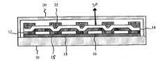
- a top-emitting OLED display deviceincludes a substrate 10 with an encapsulating cover 20 .
- Thin-film transistor (TFT) circuitry 18is located on the substrate 10 , and a patterned electrode 16 covering a portion of the substrate is located above the TFT layer 18 .
- This patterned electrode 16defines the light emitting elements of the OLED display and gaps 15 between the light emitting elements.
- a layer of OLED light emissive materials 12is coated over most of the display.
- the layer of OLED materials 12may comprise a variety of materials to emit different colors of light and may be patterned over the substrate to provide a colored display.
- the layer of OLED light emissive materials 12is composed of a plurality of layers such as hole injection and electron transport layers as is known in the art.
- a continuous transparent electrode layer 14is coated over most of the display.
- a light absorbing auxiliary electrode 22 that is thermally and electrically conductiveis located over the gaps between the light emitting areas in electrical and thermal contact with the continuous transparent electrode layer 14 .
- the light absorbing auxiliary electrode 22may be precisely aligned with the gaps 15 as shown in FIG. 1, or may be less precisely aligned.
- the auxiliary electrode 22may also be wider than the gaps to accommodate the less-precise alignment.
- located over the gapsmeans located near the gaps and at least partially overlapping the gaps.
- An optional electrode protection layer(not shown) may be provided over the electrodes 14 and 22 .
- the TFT circuitry 18controls current passing through the patterned electrode 16 , the OLED light emissive materials 12 , and the transparent electrode 14 .
- Light 30is emitted from the areas defined by the patterned electrode 16 and is not emitted from the gaps between the light emitting elements.
- the patterned electrode 16is reflective so that any light emitted toward the substrate 10 is reflected out of the display.
- the TFT circuitry 18includes power bus lines for conducting current.
- the currentpasses through the patterned electrode 16 , the layer of OLED light emissive materials 12 , and the continuous transparent electrode 14 , causing resistive heating in both the TFT circuitry 18 and in the electrodes and layer of OLED light emissive materials 14 , 16 , and 12 .
- the light absorbing auxiliary electrode 22conducts current as part of the transparent electrode 14 thereby reducing the sheet resistivity of the transparent electrode 14 and reducing the resistive heating.
- the auxiliary electrode 22is thermally conductive, the heat generated in the layer of OLED light emissive materials 12 is distributed through the auxiliary electrode 22 , thereby reducing hot spots in the display.
- This combined effect of reducing resistivity and increasing thermal conductivityreduces both the overall heat produced in the device and the heat in the OLED light emissive layer. Hence, brightness and/or lifetime of the OLED display device may be increased.
- the sharpness of the displayis also improved because unwanted, emitted light that might otherwise be internally reflected within the layers of the display device may be absorbed by the auxiliary electrode 22 .
- the transparent electrode 14may conform to the surface on which it is deposited. Planarization layers may be included to modify the surface regularity of the display.
- the light absorbing auxiliary electrode 22may conform as desired to the surface of the transparent electrode.
- the transparent electrode 14allows light to pass through.
- the light absorbing auxiliary electrode 22may be located beneath the transparent electrode 14 above the gaps 15 defined by the patterned electrode 16 .
- the present inventionmay also be employed to improve a microcavity OLED display wherein the transparent electrode 14 provides a partial mirror for the microcavity.
- one type of OLED displayincludes columns 40 of light emitting pixels, with no substantial non light emitting spaces between the pixels in a column.
- the light absorbing auxiliary electrodes 22define a vertical stripe between the columns 40 of light emitting pixels.
- Successive columns 40 of light emitting pixelsmay be of different colors, for example, repeated columns of red, green, and blue.
- the displaymay be laid out in rows.
- another type of OLED displayincludes a two dimensional array of light emitting pixels 44 , with non light emitting spaces surrounding each light emitting pixel 44 .
- the light absorbing auxiliary electrodes 22define a grid structure.
- Other arrangements, such as delta patterns,may also be used.
- the light absorbing and conductive material forming the auxiliary electrodes 22is a black silver compound.
- Silveris a highly thermally and electrically conductive material and can be made light absorbing through electrochemical processes known in the art; for example, it can be oxidized and reduced. Photographic processes may also be used.
- the deposition and patterning process for the light absorbing auxiliary electrode 22is done through the use of conventional photo-resistive processes.
- Silver compoundsare suggested in the prior art as candidates for the electrode 14 , for example magnesium silver compounds, thereby improving the chemical compatibility of the electrode and the thick film of light absorbing auxiliary electrode 22 .
- Other suitable materialsmay include aluminum, copper, magnesium, titanium, or alloys thereof.
- the light absorbermay be provided with desiccating properties, thereby improving the lifetime of the organic layers.
- the light absorbing and conductive materialcomprises two layers, a thermally and electrically conductive auxiliary electrode 50 and a light-absorbing layer 52 deposited over the conductive layer.
- the gap between the patterned electrodes 16is filled with an insulator 54 .
- the light absorbing and conductive materialcomprises two layers, a thermally and electrically conductive auxiliary electrode 50 deposited beneath the electrode 14 and a light-absorbing layer 52 deposited over the conductive layer 14 .
- the gap between the patterned electrodes 16is filled with an insulator 54 .
- Suitable conductive materialsmay include aluminum, copper, magnesium, silver, titanium, or alloys thereof.
- the light absorbing layermay include a metal oxide, metal sulfide, silicon oxide, silicon nitride, carbon, or combinations thereof.
- the light absorbing materialis black and may include further anti-reflective coatings.
- FIG. 7a cross-section of a portion of an OLED display according to the present invention is shown in more detail.
- the displayis constructed as follows. Over the substrate 10 , a semiconducting layer 80 is formed, doped, and patterned. A gate insulating layer 86 is formed over the semiconductor layer. Over the gate insulating layer, a gate conductor 82 is formed. Typical materials used to form the gate insulating layer are silicon dioxide or silicon nitride. The semiconductor layer is then doped to form source and drain regions on either sides of the gate (not shown). An interlayer insulator layer 84 is formed over the gate conductor layer. Typical materials used to form the interlayer insulator layer are silicon dioxide or silicon nitride.
- a conductor layeris deposited and patterned forming the power lines 88 and the data lines 70 .
- An interlayer insulator layer 72is formed over the conductor layer.
- the interlayer insulator layer 72preferably is a layer of planarizing material which smoothes the device topography.
- the electrode 16 of the organic light emitting elementsis formed. These electrodes are patterned to define the light emitting elements.
- the electrode 16is typically formed of a material which is both conductive and reflective, such as for example, aluminum (Al), silver (Ag), or molybdenum (Mo), gold (Au), or platinum (Pt).
- a material which is both conductive and reflectivesuch as for example, aluminum (Al), silver (Ag), or molybdenum (Mo), gold (Au), or platinum (Pt).
- an inter-pixel insulating film 54is formed to reduce shorts between the anode and the cathode. Use of such insulating films over the electrode is disclosed in U.S. Pat. No. 6,246,179, issued Jun. 12, 2001 to Yamada. While use of the inter-pixel insulating film is preferred, it is not required for successful implementation of the invention.
- the organic light emitting layers 12are deposited over the electrode 16 .
- organic EL layer structuresknown in the art wherein the present invention can be employed.
- a common configuration of the organic light emitting layersis employed in the preferred embodiment consisting of a hole injecting layer 66 , a hole transporting layer 64 , an emitting layer 62 , and an electron transporting layer 60 .
- the emitting layer 62is the only layer that requires patterning between pixels according to the technique taught in U.S. Pat. No. 6,281,634, issued Aug. 28, 2001 to Yokoyama.
- the electrode 14is located over the organic light emitting layers. In a top emitter configuration, the electrode 14 is transparent and conductive.
- the most common materials used for the electrodeis indium tin oxide (ITO) or indium zinc oxide (IZO) or a thin metal layer such as Al, Mg, or Ag which is preferably between 5 nm and 20 nm in thickness. While one layer is shown for the electrode 14 , multiple sub-layers can be combined to achieve the desired level of conductance and transparency such as an ITO layer and an Al layer.
- the electrode 14is common to all pixels and does not require precision alignment and patterning.
- the light absorbing properties of the devicemay be enhanced by the use of color filter arrays above the light emitting elements and the light absorbing areas.
- the composition and deposition of such filtersis well-known in the art.
- the conductive and/or light absorbing layersmay be deposited using techniques such as sputtering through a shadow mask. In one embodiment, the same shadow mask is used for depositing both a conductive layer and a light absorbing layer.
- the electrically and thermally conductive electrode and light absorbing layermay be deposited, patterned, and etched using a single photolithography mask step. Deposition for the conductive and/or light absorbing layers may also be done using a thermal transfer process from a donor substrate.
- the present inventionmay be applied to both active and passive matrix OLED displays.
- Planarization and/or electrode protection layersmay be placed over or under the light absorbing auxiliary electrode 22 .
- the protection layermay comprise inorganic materials such as SiOx or SiNx, for example, as disclosed in JP 2001126864.
- the protection layermay comprise organic materials such as polymers, including but not limited to, TEFLON®, polyimides, and polymers disclosed in JP 11-162634. Protection layer may comprise multiple layers of organic or inorganic materials, or combinations thereof. Alternating inorganic and organic layers, for example, as disclosed in U.S. Pat. No. 6,268,2951, issued Jul.
- the protection layershould have high optical transparency, preferably greater than 70% transmittance.
- Applicantshave demonstrated the deposition of a thick film of black silver using electroplating and chemical reduction techniques known in the art.
- the thick film of light absorbing material 22may also be deposited in a pattern using photolithographic techniques known in the art.
- light absorbing materialmay be coated as a liquid on the entire surface and exposed to radiation through a mask to polymerize portions of the coating. Portions of the material exposed to the radiation are cured and the remainder is washed away. Dry film photolithography may also be used.
- patterned thermal transfercan be used, for example, by coating material onto a donor substrate, placing the donor substrate in contact with or in close proximity to the OLED substrate, and selectively heating the donor with a laser to cause transfer of the light absorbing material to the OLED substrate.
- the light absorbing auxiliary electrode 22may comprise a plurality of thinner layers deposited by sequential deposition of light absorbing materials. Alternatively, the light absorbing auxiliary electrode 22 may be a thick film and may be deposited using screen printing methods. A light absorbing auxiliary electrode may also be provided around the perimeter of the display to further increase the contrast of the display device and conductivity of the electrode 14 .
- a color OLED displaymay be provided by an array of light emitting materials 12 that emit different colors of light.
- the color OLED displaymay be provided by a white-light emitting OLED layer together with an array of color filters to provide a color display.
- color filter materialsmay be deposited above the light absorbing auxiliary electrode 22 , as well as above the light emissive areas defined by the electrode 14 .
- a light absorbing filtermay be deposited over the light absorbing auxiliary electrode 22 to enhance the light absorption.
- transparent cover 20is typically glass or plastic sheet
- the covercan comprise materials that are deposited in a conformable manner over the surface of the materials deposited over the substrate, i.e. over OLED substrate and the light absorbing auxiliary electrode and any electrode protection layer.
- This inventioncan be advantageously practiced with active or passive matrix OLED display devices.
Landscapes
- Physics & Mathematics (AREA)
- Optics & Photonics (AREA)
- Electroluminescent Light Sources (AREA)
Abstract
Description
- The present invention relates to organic light emitting diode (OLED) displays having a plurality of pixels, and more particularly, to top-emitting displays that include an auxiliary electrode for improving the conductivity of a transparent continuous electrode in the display.[0001]
- Flat-panel displays, such as organic light emitting diode (OLED) displays, of various sizes are proposed for use in many computing and communication applications. In its simplest form, an OLED is comprised of an anode for hole injection, a cathode for electron injection, and an organic medium sandwiched between these electrodes to support charge recombination that yields emission of light. OLED displays may be constructed to emit light through a transparent substrate (commonly referred to as a bottom emitting display), or through a transparent top electrode on the top of the display (commonly referred to as a top emitting display).[0002]
- Materials for forming the transparent electrode of top emitting displays are well known in the art and include transparent conductive oxides (TCO's), such as indium tin oxide (ITO); thin layers of metal, such as Al, having a thickness on the order of 20 nm; and conductive polymers such as polythiophene. However, many electrode materials that are transparent, such as ITO, have low conductivity, which results in a voltage drop across the display. This in turn causes variable light output from the light emitting elements in the display, resistive heating, and power loss. Resistance can be lowered by increasing the thickness of the top electrode, but this decreases transparency.[0003]
- One proposed solution to this problem is to use an auxiliary electrode above or below the transparent electrode layer and located between the pixels, as taught by US2002/0011783, published Jan. 31, 2002, by Hosokawa. The auxiliary electrode is not required to be transparent and therefore can be of a higher conductivity than the transparent electrode. The auxiliary electrode is typically constructed of conductive metals (Al, Ag, Cu, Au) that are also highly reflective. This results in incident light reflecting off the auxiliary electrode and thereby reducing the overall contrast ratio of the display. This makes the display less effective for use under high ambient light conditions, such as outdoors under sunshine.[0004]
- There is a need therefore for an improved top emitting OLED display that uses an auxiliary electrode and has improved contrast.[0005]
- The need is met according to the present invention by providing a top emitting OLED display that includes a substrate; a patterned electrode formed above the substrate, defining a plurality of light emitting elements having gaps between the light emitting elements; a layer of OLED material disposed above the patterned electrode; a continuous transparent electrode disposed above the layer of OLED material; and a light-absorbing auxiliary electrode that is thermally and electrically conductive and in electrical and thermal contact with the continuous transparent electrode and located over the gaps between the light emitting elements of the display.[0006]
- This invention has the advantage over other top emission devices having auxiliary electrodes of improved contrast and heat dissipation and therefore improved usability in bright ambient conditions such as in sunlight.[0007]
- FIG. 1 is a cross sectional schematic diagram of an OLED display device according to one embodiment of the present invention;[0008]
- FIG. 2 is a partial cross sectional schematic diagram of an OLED display device according to another embodiment of the present invention;[0009]
- FIG. 3 is a plan view of an auxiliary electrode according to one embodiment of the present invention;[0010]
- FIG. 4 is a plan view of an auxiliary electrode according to another embodiment of the present invention;[0011]
- FIG. 5 is a partial cross sectional schematic diagram of an OLED display device according to a further alternative embodiment of the present invention;[0012]
- FIG. 6 is a partial cross sectional schematic diagram of an OLED display device according to still further alternative embodiment of the present invention; and[0013]
- FIG. 7 is a more detailed partial cross sectional schematic diagram of the OLED display device shown FIG. 5.[0014]
- It will be understood that the figures are not to scale since the individual layers are too thin and the thickness differences of various layers too great to permit depiction to scale.[0015]
- Referring to FIG. 1 a top-emitting OLED display device according to the present invention includes a[0016]
substrate 10 with an encapsulatingcover 20. Thin-film transistor (TFT)circuitry 18 is located on thesubstrate 10, and a patternedelectrode 16 covering a portion of the substrate is located above theTFT layer 18. This patternedelectrode 16 defines the light emitting elements of the OLED display andgaps 15 between the light emitting elements. A layer of OLED lightemissive materials 12 is coated over most of the display. The layer ofOLED materials 12 may comprise a variety of materials to emit different colors of light and may be patterned over the substrate to provide a colored display. The layer of OLED lightemissive materials 12 is composed of a plurality of layers such as hole injection and electron transport layers as is known in the art. A continuoustransparent electrode layer 14 is coated over most of the display. A light absorbingauxiliary electrode 22 that is thermally and electrically conductive is located over the gaps between the light emitting areas in electrical and thermal contact with the continuoustransparent electrode layer 14. The light absorbingauxiliary electrode 22 may be precisely aligned with thegaps 15 as shown in FIG. 1, or may be less precisely aligned. Theauxiliary electrode 22 may also be wider than the gaps to accommodate the less-precise alignment. As used herein the term “located over the gaps” means located near the gaps and at least partially overlapping the gaps. An optional electrode protection layer (not shown) may be provided over theelectrodes - In operation, the[0017]
TFT circuitry 18 controls current passing through the patternedelectrode 16, the OLED lightemissive materials 12, and thetransparent electrode 14.Light 30 is emitted from the areas defined by the patternedelectrode 16 and is not emitted from the gaps between the light emitting elements. In one embodiment, the patternedelectrode 16 is reflective so that any light emitted toward thesubstrate 10 is reflected out of the display. - The[0018]
TFT circuitry 18 includes power bus lines for conducting current. The current passes through thepatterned electrode 16, the layer of OLED lightemissive materials 12, and the continuoustransparent electrode 14, causing resistive heating in both theTFT circuitry 18 and in the electrodes and layer of OLED lightemissive materials auxiliary electrode 22 conducts current as part of thetransparent electrode 14 thereby reducing the sheet resistivity of thetransparent electrode 14 and reducing the resistive heating. Moreover, because theauxiliary electrode 22 is thermally conductive, the heat generated in the layer of OLED lightemissive materials 12 is distributed through theauxiliary electrode 22, thereby reducing hot spots in the display. This combined effect of reducing resistivity and increasing thermal conductivity reduces both the overall heat produced in the device and the heat in the OLED light emissive layer. Hence, brightness and/or lifetime of the OLED display device may be increased. The sharpness of the display is also improved because unwanted, emitted light that might otherwise be internally reflected within the layers of the display device may be absorbed by theauxiliary electrode 22. - Since any ambient light incident on the display between the light emissive portions of the display is absorbed by the light absorbing auxiliary electrode, the ambient contrast of the display is also increased according to the present invention. As shown in FIG. 1, the[0019]
transparent electrode 14 may conform to the surface on which it is deposited. Planarization layers may be included to modify the surface regularity of the display. The light absorbingauxiliary electrode 22 may conform as desired to the surface of the transparent electrode. Thetransparent electrode 14 allows light to pass through. - Referring to FIG. 2, the light absorbing[0020]
auxiliary electrode 22 may be located beneath thetransparent electrode 14 above thegaps 15 defined by the patternedelectrode 16. - The present invention may also be employed to improve a microcavity OLED display wherein the[0021]
transparent electrode 14 provides a partial mirror for the microcavity. - Referring to FIG. 3, one type of OLED display includes[0022]
columns 40 of light emitting pixels, with no substantial non light emitting spaces between the pixels in a column. For this configuration, the light absorbingauxiliary electrodes 22 define a vertical stripe between thecolumns 40 of light emitting pixels.Successive columns 40 of light emitting pixels may be of different colors, for example, repeated columns of red, green, and blue. Alternatively, the display may be laid out in rows. - Referring to FIG. 4, another type of OLED display includes a two dimensional array of[0023]
light emitting pixels 44, with non light emitting spaces surrounding eachlight emitting pixel 44. For this configuration, the light absorbingauxiliary electrodes 22 define a grid structure. Other arrangements, such as delta patterns, may also be used. - In one embodiment, the light absorbing and conductive material forming the[0024]
auxiliary electrodes 22 is a black silver compound. Silver is a highly thermally and electrically conductive material and can be made light absorbing through electrochemical processes known in the art; for example, it can be oxidized and reduced. Photographic processes may also be used. The deposition and patterning process for the light absorbingauxiliary electrode 22 is done through the use of conventional photo-resistive processes. Silver compounds are suggested in the prior art as candidates for theelectrode 14, for example magnesium silver compounds, thereby improving the chemical compatibility of the electrode and the thick film of light absorbingauxiliary electrode 22. Other suitable materials may include aluminum, copper, magnesium, titanium, or alloys thereof. - In a further embodiment of the present invention, the light absorber may be provided with desiccating properties, thereby improving the lifetime of the organic layers.[0025]
- Referring to FIG. 5, in an alternative embodiment, the light absorbing and conductive material comprises two layers, a thermally and electrically conductive[0026]
auxiliary electrode 50 and a light-absorbinglayer 52 deposited over the conductive layer. The gap between thepatterned electrodes 16 is filled with aninsulator 54. - Referring to FIG. 6, in another alternative embodiment, the light absorbing and conductive material comprises two layers, a thermally and electrically conductive[0027]
auxiliary electrode 50 deposited beneath theelectrode 14 and a light-absorbinglayer 52 deposited over theconductive layer 14. The gap between thepatterned electrodes 16 is filled with aninsulator 54. Suitable conductive materials may include aluminum, copper, magnesium, silver, titanium, or alloys thereof. The light absorbing layer may include a metal oxide, metal sulfide, silicon oxide, silicon nitride, carbon, or combinations thereof. Preferably, the light absorbing material is black and may include further anti-reflective coatings. - Referring to FIG. 7, a cross-section of a portion of an OLED display according to the present invention is shown in more detail. The display is constructed as follows. Over the[0028]
substrate 10, asemiconducting layer 80 is formed, doped, and patterned. Agate insulating layer 86 is formed over the semiconductor layer. Over the gate insulating layer, agate conductor 82 is formed. Typical materials used to form the gate insulating layer are silicon dioxide or silicon nitride. The semiconductor layer is then doped to form source and drain regions on either sides of the gate (not shown). Aninterlayer insulator layer 84 is formed over the gate conductor layer. Typical materials used to form the interlayer insulator layer are silicon dioxide or silicon nitride. - Over the[0029]
interlayer insulator layer 84, a conductor layer is deposited and patterned forming thepower lines 88 and the data lines70. Aninterlayer insulator layer 72 is formed over the conductor layer. Theinterlayer insulator layer 72 preferably is a layer of planarizing material which smoothes the device topography. Over the interlayer insulator layer, theelectrode 16 of the organic light emitting elements is formed. These electrodes are patterned to define the light emitting elements. - For a top emitting display (i.e. a display that emits light from the side of the substrate on which the OLEDs are located), the[0030]
electrode 16 is typically formed of a material which is both conductive and reflective, such as for example, aluminum (Al), silver (Ag), or molybdenum (Mo), gold (Au), or platinum (Pt). Around the edges of the electrodes, an inter-pixelinsulating film 54 is formed to reduce shorts between the anode and the cathode. Use of such insulating films over the electrode is disclosed in U.S. Pat. No. 6,246,179, issued Jun. 12, 2001 to Yamada. While use of the inter-pixel insulating film is preferred, it is not required for successful implementation of the invention. - The organic[0031]
light emitting layers 12 are deposited over theelectrode 16. There are numerous organic EL layer structures known in the art wherein the present invention can be employed. A common configuration of the organic light emitting layers is employed in the preferred embodiment consisting of ahole injecting layer 66, ahole transporting layer 64, an emittinglayer 62, and anelectron transporting layer 60. As is shown in FIG. 7, the emittinglayer 62 is the only layer that requires patterning between pixels according to the technique taught in U.S. Pat. No. 6,281,634, issued Aug. 28, 2001 to Yokoyama. - The[0032]
electrode 14 is located over the organic light emitting layers. In a top emitter configuration, theelectrode 14 is transparent and conductive. The most common materials used for the electrode is indium tin oxide (ITO) or indium zinc oxide (IZO) or a thin metal layer such as Al, Mg, or Ag which is preferably between 5 nm and 20 nm in thickness. While one layer is shown for theelectrode 14, multiple sub-layers can be combined to achieve the desired level of conductance and transparency such as an ITO layer and an Al layer. Theelectrode 14 is common to all pixels and does not require precision alignment and patterning. - The light absorbing properties of the device may be enhanced by the use of color filter arrays above the light emitting elements and the light absorbing areas. The composition and deposition of such filters is well-known in the art.[0033]
- The conductive and/or light absorbing layers may be deposited using techniques such as sputtering through a shadow mask. In one embodiment, the same shadow mask is used for depositing both a conductive layer and a light absorbing layer. Alternatively, the electrically and thermally conductive electrode and light absorbing layer may be deposited, patterned, and etched using a single photolithography mask step. Deposition for the conductive and/or light absorbing layers may also be done using a thermal transfer process from a donor substrate.[0034]
- The present invention may be applied to both active and passive matrix OLED displays. Planarization and/or electrode protection layers may be placed over or under the light absorbing[0035]
auxiliary electrode 22. When provided, the protection layer may comprise inorganic materials such as SiOx or SiNx, for example, as disclosed in JP 2001126864. Alternatively, the protection layer may comprise organic materials such as polymers, including but not limited to, TEFLON®, polyimides, and polymers disclosed in JP 11-162634. Protection layer may comprise multiple layers of organic or inorganic materials, or combinations thereof. Alternating inorganic and organic layers, for example, as disclosed in U.S. Pat. No. 6,268,2951, issued Jul. 31, 2001 to Ohta et al., and WO 00/36665, by Graff et al., published Jun. 22, 2000, are useful as protection layer. In all cases, the protection layer should have high optical transparency, preferably greater than 70% transmittance. - Applicants have demonstrated the deposition of a thick film of black silver using electroplating and chemical reduction techniques known in the art. The thick film of[0036]
light absorbing material 22 may also be deposited in a pattern using photolithographic techniques known in the art. For example, light absorbing material may be coated as a liquid on the entire surface and exposed to radiation through a mask to polymerize portions of the coating. Portions of the material exposed to the radiation are cured and the remainder is washed away. Dry film photolithography may also be used. In addition, patterned thermal transfer can be used, for example, by coating material onto a donor substrate, placing the donor substrate in contact with or in close proximity to the OLED substrate, and selectively heating the donor with a laser to cause transfer of the light absorbing material to the OLED substrate. The light absorbingauxiliary electrode 22 may comprise a plurality of thinner layers deposited by sequential deposition of light absorbing materials. Alternatively, the light absorbingauxiliary electrode 22 may be a thick film and may be deposited using screen printing methods. A light absorbing auxiliary electrode may also be provided around the perimeter of the display to further increase the contrast of the display device and conductivity of theelectrode 14. - A color OLED display may be provided by an array of[0037]
light emitting materials 12 that emit different colors of light. Alternatively, the color OLED display may be provided by a white-light emitting OLED layer together with an array of color filters to provide a color display. In this embodiment, color filter materials may be deposited above the light absorbingauxiliary electrode 22, as well as above the light emissive areas defined by theelectrode 14. In addition, a light absorbing filter may be deposited over the light absorbingauxiliary electrode 22 to enhance the light absorption. - While[0038]
transparent cover 20 is typically glass or plastic sheet, the cover can comprise materials that are deposited in a conformable manner over the surface of the materials deposited over the substrate, i.e. over OLED substrate and the light absorbing auxiliary electrode and any electrode protection layer. - This invention can be advantageously practiced with active or passive matrix OLED display devices.[0039]
- The invention has been described in detail with particular reference to certain preferred embodiments thereof, but it will be understood that variations and modifications can be effected within the spirit and scope of the invention.[0040]
10 substrate 12 OLED light emissive materials 14 electrode 15 gap 16 electrode 18 TFT circuitry 20 encapsulating cover 22 auxiliary electrode 30 light 40 columns 44 light emitting pixel 50 thermally and electrically conductive auxiliary electrode 52 light absorbing layer 54 inter-pixel insulating film 60 electron transporting layer 62 emitting layer 64 hole transporting layer 66 hole injecting layer 70 data line 72 insulator layer 80 semiconducting layer 82 conductor 84 interlayer insulator layer 86 insulating layer 88 power line
Claims (34)
Priority Applications (2)
| Application Number | Priority Date | Filing Date | Title |
|---|---|---|---|
| US10/388,111US6812637B2 (en) | 2003-03-13 | 2003-03-13 | OLED display with auxiliary electrode |
| JP2004071163AJP2004281402A (en) | 2003-03-13 | 2004-03-12 | Top-emitting organic light emitting diode (OLED) display |
Applications Claiming Priority (1)
| Application Number | Priority Date | Filing Date | Title |
|---|---|---|---|
| US10/388,111US6812637B2 (en) | 2003-03-13 | 2003-03-13 | OLED display with auxiliary electrode |
Publications (2)
| Publication Number | Publication Date |
|---|---|
| US20040178722A1true US20040178722A1 (en) | 2004-09-16 |
| US6812637B2 US6812637B2 (en) | 2004-11-02 |
Family
ID=32962061
Family Applications (1)
| Application Number | Title | Priority Date | Filing Date |
|---|---|---|---|
| US10/388,111Expired - LifetimeUS6812637B2 (en) | 2003-03-13 | 2003-03-13 | OLED display with auxiliary electrode |
Country Status (2)
| Country | Link |
|---|---|
| US (1) | US6812637B2 (en) |
| JP (1) | JP2004281402A (en) |
Cited By (25)
| Publication number | Priority date | Publication date | Assignee | Title |
|---|---|---|---|---|
| FR2879025A1 (en)* | 2004-12-07 | 2006-06-09 | Thomson Licensing Sa | ORGANIC ELECTROLUMINESCENT DIODE AND DIODE PANEL WITH ANTI-REFLECTIVE LAYER PROMOTING LIGHT EXTRACTION |
| US20070042528A1 (en)* | 2005-08-20 | 2007-02-22 | Lambright Terry M | Defining electrode regions of electroluminescent panel |
| WO2007008946A3 (en)* | 2005-07-12 | 2007-03-22 | Eastman Kodak Co | Oled device having spacers |
| US20080157664A1 (en)* | 2006-12-27 | 2008-07-03 | Cok Ronald S | Oled with protective bi-layer electrode |
| US20080224607A1 (en)* | 2007-03-14 | 2008-09-18 | Sony Corporation | Display |
| US20080303420A1 (en)* | 2007-03-19 | 2008-12-11 | Seiko Epson Corporation | Organic el device, line head, and electronic apparatus |
| US20090066236A1 (en)* | 2007-09-11 | 2009-03-12 | Un-Cheol Sung | Organic light-emitting display device and method of manufacturing the same |
| US20090072711A1 (en)* | 2004-05-17 | 2009-03-19 | Salvatore Cina | Organic light-emitting diode (oled) with improved light extraction and corresponding display unit |
| US20100084969A1 (en)* | 2008-10-02 | 2010-04-08 | Jun-Ho Choi | Organic light emitting display and method of manufacturing the same |
| US20100127273A1 (en)* | 2005-05-11 | 2010-05-27 | Lg Display Co., Ltd. | Light emitting device and manufacturing method thereof and light emitting display and manufacturing method thereof |
| US20100243997A1 (en)* | 2007-06-14 | 2010-09-30 | Rohm Co., Ltd. | Organic electroluminescence device and its manufacturing method |
| US20110260954A1 (en)* | 2010-04-26 | 2011-10-27 | Sok Won Noh | Organic light-emitting display apparatus |
| US20110303930A1 (en)* | 2010-06-11 | 2011-12-15 | Samsung Mobile Display Co., Ltd. | Organic light emitting diode display |
| WO2011159160A1 (en)* | 2010-06-17 | 2011-12-22 | Nederlandse Organisatie Voor Toegepast-Natuurwetenschappelijk Onderzoek Tno | Opto-electric device and method of manufacturing thereof |
| KR101243924B1 (en) | 2010-04-26 | 2013-03-14 | 삼성디스플레이 주식회사 | Organic light emitting display apparatus |
| CN103563486A (en)* | 2011-05-20 | 2014-02-05 | 松下电器产业株式会社 | organic electroluminescent element |
| WO2016113097A1 (en)* | 2015-01-13 | 2016-07-21 | Osram Oled Gmbh | Organic light-emitting component |
| US20170077438A1 (en)* | 2014-05-15 | 2017-03-16 | Lg Display Co., Ltd. | Organic light emitting device |
| US20170155077A1 (en)* | 2015-05-06 | 2017-06-01 | Shenzhen China Star Optoelectronics Technology Co., Ltd. | Flexible oled and manufacture method thereof |
| US20180205036A1 (en)* | 2015-06-17 | 2018-07-19 | Universal Display Corporation | Flexible amoled display |
| US20180342698A1 (en)* | 2017-05-26 | 2018-11-29 | Shenzhen China Star Optoelectronics Technology Co., Ltd. | Oled device packaging component, packaging method and display device thereof |
| CN109817833A (en)* | 2019-02-27 | 2019-05-28 | 云谷(固安)科技有限公司 | Display device, display panel and display device |
| US10319935B2 (en) | 2017-04-05 | 2019-06-11 | Joled Inc. | Organic EL display panel and method of manufacturing organic EL display panel |
| CN114023909A (en)* | 2021-11-03 | 2022-02-08 | 昆山工研院新型平板显示技术中心有限公司 | Display panel and electronic device |
| US12161038B2 (en)* | 2022-07-21 | 2024-12-03 | Samsung Display Co., Ltd. | Display device |
Families Citing this family (139)
| Publication number | Priority date | Publication date | Assignee | Title |
|---|---|---|---|---|
| TW511298B (en)* | 1999-12-15 | 2002-11-21 | Semiconductor Energy Lab | EL display device |
| US7098069B2 (en) | 2002-01-24 | 2006-08-29 | Semiconductor Energy Laboratory Co., Ltd. | Light emitting device, method of preparing the same and device for fabricating the same |
| SG143063A1 (en)* | 2002-01-24 | 2008-06-27 | Semiconductor Energy Lab | Light emitting device and method of manufacturing the same |
| EP1343206B1 (en) | 2002-03-07 | 2016-10-26 | Semiconductor Energy Laboratory Co., Ltd. | Light emitting apparatus, electronic apparatus, illuminating device and method of fabricating the light emitting apparatus |
| TW588571B (en)* | 2002-05-24 | 2004-05-21 | Sanyo Electric Co | Electroluminescence display device |
| WO2004026002A1 (en)* | 2002-09-11 | 2004-03-25 | Semiconductor Energy Laboratory Co., Ltd. | Light-emitting apparatus and fabrication method of the same |
| JP4434563B2 (en)* | 2002-09-12 | 2010-03-17 | パイオニア株式会社 | Manufacturing method of organic EL display device |
| JP2005019211A (en) | 2003-06-26 | 2005-01-20 | Casio Comput Co Ltd | EL display panel and method of manufacturing EL display panel |
| US7030553B2 (en)* | 2003-08-19 | 2006-04-18 | Eastman Kodak Company | OLED device having microcavity gamut subpixels and a within gamut subpixel |
| JP4716699B2 (en)* | 2003-09-30 | 2011-07-06 | 三洋電機株式会社 | Organic EL panel |
| JP4497881B2 (en)* | 2003-09-30 | 2010-07-07 | 三洋電機株式会社 | Organic EL device and organic EL panel |
| KR100552972B1 (en)* | 2003-10-09 | 2006-02-15 | 삼성에스디아이 주식회사 | Flat panel display and manufacturing method |
| JP4600284B2 (en)* | 2003-10-28 | 2010-12-15 | 住友金属鉱山株式会社 | Transparent conductive laminate, manufacturing method thereof, and device using transparent conductive laminate |
| JP4439260B2 (en)* | 2003-12-26 | 2010-03-24 | 三洋電機株式会社 | Manufacturing method of display device |
| JP2005197009A (en)* | 2003-12-26 | 2005-07-21 | Sanyo Electric Co Ltd | Display device, manufacturing method thereof, and manufacturing device |
| US20050156512A1 (en)* | 2003-12-30 | 2005-07-21 | Vadim Savvateev | Electroluminescent devices with at least one electrode having apertures and methods of using such devices |
| TWI272039B (en)* | 2004-06-18 | 2007-01-21 | Sanyo Electric Co | Electroluminescence panel |
| JP2006164808A (en)* | 2004-12-09 | 2006-06-22 | Hitachi Ltd | LIGHT EMITTING ELEMENT, LIGHTING DEVICE, AND DISPLAY DEVICE HAVING THE SAME |
| KR100686075B1 (en) | 2005-02-22 | 2007-02-26 | 엘지전자 주식회사 | Top emission type active matrix organic electroluminescent display device and manufacturing method thereof |
| JP4573672B2 (en)* | 2005-02-28 | 2010-11-04 | 三洋電機株式会社 | Organic EL panel |
| TWI282699B (en)* | 2005-03-14 | 2007-06-11 | Au Optronics Corp | Method of fabrication organic light emitting diode display |
| PL3770980T3 (en)* | 2005-05-20 | 2024-11-12 | Signify Holding B.V. | Lighting-emitting module |
| US9166197B2 (en)* | 2005-08-29 | 2015-10-20 | The Hong Kong University Of Science And Technology | Metallic anode treated by carbon tetrafluoride plasma for organic light emitting device |
| US7498735B2 (en)* | 2005-10-18 | 2009-03-03 | Eastman Kodak Company | OLED device having improved power distribution |
| US7612496B2 (en)* | 2005-12-19 | 2009-11-03 | Eastman Kodak Company | OLED device having improved power distribution |
| JP2007273261A (en)* | 2006-03-31 | 2007-10-18 | Hitachi Displays Ltd | Organic EL display device |
| US7652681B2 (en)* | 2006-04-11 | 2010-01-26 | Tpo Displays Corp. | Systems for displaying images involving display panels |
| KR100778443B1 (en) | 2006-07-10 | 2007-11-21 | 삼성에스디아이 주식회사 | Organic light emitting display |
| US8053971B2 (en)* | 2006-07-31 | 2011-11-08 | Lg Display Co., Ltd. | Organic light emitting device and method of fabricating the same |
| US20100252841A1 (en)* | 2006-09-18 | 2010-10-07 | Cok Ronald S | Oled device having improved lifetime and resolution |
| US7633218B2 (en) | 2006-09-29 | 2009-12-15 | Eastman Kodak Company | OLED device having improved lifetime and resolution |
| JP2008108530A (en) | 2006-10-25 | 2008-05-08 | Hitachi Displays Ltd | Organic EL display device |
| US20080278063A1 (en)* | 2007-05-07 | 2008-11-13 | Cok Ronald S | Electroluminescent device having improved power distribution |
| US7432187B1 (en) | 2007-05-14 | 2008-10-07 | Eastman Kodak Company | Method for improving current distribution of a transparent electrode |
| US7722422B2 (en)* | 2007-05-21 | 2010-05-25 | Global Oled Technology Llc | Device and method for improved power distribution for a transparent electrode |
| US7982396B2 (en) | 2007-06-04 | 2011-07-19 | Global Oled Technology Llc | Light-emitting device with light-scattering particles and method of making the same |
| JP2009026619A (en)* | 2007-07-20 | 2009-02-05 | Hitachi Displays Ltd | Organic EL display device |
| KR100964225B1 (en) | 2008-03-19 | 2010-06-17 | 삼성모바일디스플레이주식회사 | Organic light emitting display device |
| US20090278454A1 (en)* | 2008-05-12 | 2009-11-12 | Fedorovskaya Elena A | Oled display encapsulated with a filter |
| EP2244317A1 (en)* | 2009-04-23 | 2010-10-27 | Nederlandse Organisatie voor toegepast -natuurwetenschappelijk onderzoek TNO | Optoelectric device and method for manufacturing the same |
| KR101065410B1 (en)* | 2009-07-28 | 2011-09-16 | 삼성모바일디스플레이주식회사 | Organic light emitting display |
| EP2504872A1 (en) | 2009-11-27 | 2012-10-03 | Koninklijke Philips Electronics N.V. | Organic electroluminescent devices |
| JP5969745B2 (en)* | 2010-09-10 | 2016-08-17 | 株式会社半導体エネルギー研究所 | Semiconductor device |
| US9899329B2 (en) | 2010-11-23 | 2018-02-20 | X-Celeprint Limited | Interconnection structures and methods for transfer-printed integrated circuit elements with improved interconnection alignment tolerance |
| JP5888243B2 (en)* | 2011-01-17 | 2016-03-16 | コニカミノルタ株式会社 | Organic electroluminescence device |
| US8889485B2 (en) | 2011-06-08 | 2014-11-18 | Semprius, Inc. | Methods for surface attachment of flipped active componenets |
| US8710854B2 (en) | 2011-11-29 | 2014-04-29 | Eastman Kodak Company | Making transparent capacitor with multi-layer grid |
| US9046974B2 (en) | 2012-02-28 | 2015-06-02 | Eastman Kodak Company | Transparent touch-screen capacitor with micro-wire electrode |
| US8884918B2 (en) | 2012-02-28 | 2014-11-11 | Eastman Kodak Company | Electronic device having metallic micro-wires |
| US8952263B2 (en) | 2012-08-10 | 2015-02-10 | Eastman Kodak Company | Micro-wire electrode pattern |
| US8773392B2 (en) | 2012-02-28 | 2014-07-08 | Eastman Kodak Company | Transparent touch-responsive capacitor with variable-pattern micro-wires |
| US8836668B2 (en) | 2012-02-28 | 2014-09-16 | Eastman Kodak Company | Transparent touch-responsive capacitor with variable-height micro-wires |
| US8819927B2 (en) | 2012-02-28 | 2014-09-02 | Eastman Kodak Company | Method of making a transparent conductor structure |
| US8773393B2 (en) | 2012-02-28 | 2014-07-08 | Eastman Kodak Company | Touch screen with dummy micro-wires |
| US8937604B2 (en) | 2012-02-28 | 2015-01-20 | Eastman Kodak Company | Touch-responsive capacitor with polarizing dielectric structure |
| US8943682B2 (en) | 2012-02-28 | 2015-02-03 | Eastman Kodak Company | Making micro-wires with different heights |
| US8661662B1 (en) | 2012-08-10 | 2014-03-04 | Eastman Kodak Company | Making transparent touch-responsive device with micro-wire electrodes |
| US8773395B2 (en) | 2012-04-24 | 2014-07-08 | Eastman Kodak Company | Touch-responsive capacitor with polarizing dielectric method |
| US8704232B2 (en) | 2012-06-12 | 2014-04-22 | Apple Inc. | Thin film transistor with increased doping regions |
| US9065077B2 (en) | 2012-06-15 | 2015-06-23 | Apple, Inc. | Back channel etch metal-oxide thin film transistor and process |
| US9030438B2 (en) | 2012-08-16 | 2015-05-12 | Eastman Kodak Company | Pixel-aligned micro-wire electrode device |
| US9477352B2 (en) | 2012-08-10 | 2016-10-25 | Eastman Kodak Company | Making display device with pixel-aligned micro-wire electrode |
| US9098154B2 (en) | 2012-08-10 | 2015-08-04 | Eastman Kodak Company | Display apparatus with pixel-aligned micro-wire electrode |
| US8922512B2 (en) | 2012-08-16 | 2014-12-30 | Eastman Kodak Company | Display apparatus with diamond-patterned micro-wire electrode |
| US9024918B2 (en)* | 2012-08-16 | 2015-05-05 | Eastman Kodak Company | Display apparatus with pixel-aligned electrode |
| US8585455B1 (en) | 2012-09-26 | 2013-11-19 | Eastman Kodak Company | Making display device with pixel-aligned ground micro-wire |
| US9158420B2 (en) | 2012-08-22 | 2015-10-13 | Eastman Kodak Company | Pixel-aligned diamond-patterned micro-wire electrode |
| US9134860B2 (en) | 2012-08-16 | 2015-09-15 | Eastman Kodak Company | Method of making a display device |
| US9092088B2 (en) | 2012-08-16 | 2015-07-28 | Eastman Kodak Company | Pixel-aligned ground micro-wire device |
| US9244558B2 (en) | 2012-08-16 | 2016-01-26 | Eastman Kodak Company | Pixel-aligned electrode device |
| US8854327B2 (en) | 2012-09-26 | 2014-10-07 | Eastman Kodak Company | Display apparatus with pixel-aligned ground micro-wire |
| US8987027B2 (en) | 2012-08-31 | 2015-03-24 | Apple Inc. | Two doping regions in lightly doped drain for thin film transistors and associated doping processes |
| US9685557B2 (en) | 2012-08-31 | 2017-06-20 | Apple Inc. | Different lightly doped drain length control for self-align light drain doping process |
| US8591279B1 (en)* | 2012-10-19 | 2013-11-26 | Eastman Kodak Company | Making display apparatus with pixel-aligned ground mesh |
| US9164630B2 (en) | 2012-09-26 | 2015-10-20 | Eastman Kodak Company | Display apparatus with pixel-aligned ground mesh |
| US8748320B2 (en) | 2012-09-27 | 2014-06-10 | Apple Inc. | Connection to first metal layer in thin film transistor process |
| US8999771B2 (en) | 2012-09-28 | 2015-04-07 | Apple Inc. | Protection layer for halftone process of third metal |
| US9201276B2 (en) | 2012-10-17 | 2015-12-01 | Apple Inc. | Process architecture for color filter array in active matrix liquid crystal display |
| KR101995729B1 (en)* | 2012-11-29 | 2019-07-04 | 삼성디스플레이 주식회사 | Organic Electroluminescence Device |
| US9001297B2 (en) | 2013-01-29 | 2015-04-07 | Apple Inc. | Third metal layer for thin film transistor with reduced defects in liquid crystal display |
| US9088003B2 (en) | 2013-03-06 | 2015-07-21 | Apple Inc. | Reducing sheet resistance for common electrode in top emission organic light emitting diode display |
| JP2016523442A (en)* | 2013-06-29 | 2016-08-08 | アイクストロン、エスイー | High performance coating deposition method and encapsulated electronic device |
| US9444015B2 (en) | 2014-06-18 | 2016-09-13 | X-Celeprint Limited | Micro assembled LED displays and lighting elements |
| WO2016030422A1 (en) | 2014-08-26 | 2016-03-03 | X-Celeprint Limited | Micro assembled hybrid displays and lighting elements |
| US9799719B2 (en) | 2014-09-25 | 2017-10-24 | X-Celeprint Limited | Active-matrix touchscreen |
| US9537069B1 (en) | 2014-09-25 | 2017-01-03 | X-Celeprint Limited | Inorganic light-emitting diode with encapsulating reflector |
| US9991163B2 (en) | 2014-09-25 | 2018-06-05 | X-Celeprint Limited | Small-aperture-ratio display with electrical component |
| US9799261B2 (en) | 2014-09-25 | 2017-10-24 | X-Celeprint Limited | Self-compensating circuit for faulty display pixels |
| US9818725B2 (en) | 2015-06-01 | 2017-11-14 | X-Celeprint Limited | Inorganic-light-emitter display with integrated black matrix |
| CN105702875B (en) | 2014-12-11 | 2018-04-27 | 财团法人工业技术研究院 | Light-emitting element, electrode structure and manufacturing method thereof |
| KR102417266B1 (en)* | 2015-01-27 | 2022-07-05 | 삼성디스플레이 주식회사 | Display device and touch sensing method thereof |
| JP2016207452A (en)* | 2015-04-22 | 2016-12-08 | ソニー株式会社 | Display device manufacturing method, display device, and electronic apparatus |
| US9871345B2 (en) | 2015-06-09 | 2018-01-16 | X-Celeprint Limited | Crystalline color-conversion device |
| US11061276B2 (en) | 2015-06-18 | 2021-07-13 | X Display Company Technology Limited | Laser array display |
| US10133426B2 (en) | 2015-06-18 | 2018-11-20 | X-Celeprint Limited | Display with micro-LED front light |
| US10255834B2 (en) | 2015-07-23 | 2019-04-09 | X-Celeprint Limited | Parallel redundant chiplet system for controlling display pixels |
| US9640108B2 (en) | 2015-08-25 | 2017-05-02 | X-Celeprint Limited | Bit-plane pulse width modulated digital display system |
| US10380930B2 (en) | 2015-08-24 | 2019-08-13 | X-Celeprint Limited | Heterogeneous light emitter display system |
| US9865671B2 (en) | 2015-09-03 | 2018-01-09 | Industrial Technology Research Institute | Organic light-emitting device |
| US10230048B2 (en) | 2015-09-29 | 2019-03-12 | X-Celeprint Limited | OLEDs for micro transfer printing |
| US10066819B2 (en) | 2015-12-09 | 2018-09-04 | X-Celeprint Limited | Micro-light-emitting diode backlight system |
| US10091446B2 (en) | 2015-12-23 | 2018-10-02 | X-Celeprint Limited | Active-matrix displays with common pixel control |
| US9786646B2 (en) | 2015-12-23 | 2017-10-10 | X-Celeprint Limited | Matrix addressed device repair |
| US9930277B2 (en) | 2015-12-23 | 2018-03-27 | X-Celeprint Limited | Serial row-select matrix-addressed system |
| US9928771B2 (en) | 2015-12-24 | 2018-03-27 | X-Celeprint Limited | Distributed pulse width modulation control |
| US10200013B2 (en) | 2016-02-18 | 2019-02-05 | X-Celeprint Limited | Micro-transfer-printed acoustic wave filter device |
| US10361677B2 (en) | 2016-02-18 | 2019-07-23 | X-Celeprint Limited | Transverse bulk acoustic wave filter |
| US10109753B2 (en) | 2016-02-19 | 2018-10-23 | X-Celeprint Limited | Compound micro-transfer-printed optical filter device |
| TWI710061B (en) | 2016-02-25 | 2020-11-11 | 愛爾蘭商艾克斯展示公司技術有限公司 | Efficiently micro-transfer printing micro-scale devices onto large-format substrates |
| US10193025B2 (en) | 2016-02-29 | 2019-01-29 | X-Celeprint Limited | Inorganic LED pixel structure |
| US10150326B2 (en) | 2016-02-29 | 2018-12-11 | X-Celeprint Limited | Hybrid document with variable state |
| US10150325B2 (en) | 2016-02-29 | 2018-12-11 | X-Celeprint Limited | Hybrid banknote with electronic indicia |
| US10153257B2 (en) | 2016-03-03 | 2018-12-11 | X-Celeprint Limited | Micro-printed display |
| US10153256B2 (en) | 2016-03-03 | 2018-12-11 | X-Celeprint Limited | Micro-transfer printable electronic component |
| US10199546B2 (en) | 2016-04-05 | 2019-02-05 | X-Celeprint Limited | Color-filter device |
| US10008483B2 (en) | 2016-04-05 | 2018-06-26 | X-Celeprint Limited | Micro-transfer printed LED and color filter structure |
| US9997102B2 (en) | 2016-04-19 | 2018-06-12 | X-Celeprint Limited | Wirelessly powered display and system |
| US10198890B2 (en) | 2016-04-19 | 2019-02-05 | X-Celeprint Limited | Hybrid banknote with electronic indicia using near-field-communications |
| US10360846B2 (en) | 2016-05-10 | 2019-07-23 | X-Celeprint Limited | Distributed pulse-width modulation system with multi-bit digital storage and output device |
| US9997501B2 (en) | 2016-06-01 | 2018-06-12 | X-Celeprint Limited | Micro-transfer-printed light-emitting diode device |
| US10453826B2 (en) | 2016-06-03 | 2019-10-22 | X-Celeprint Limited | Voltage-balanced serial iLED pixel and display |
| US11137641B2 (en) | 2016-06-10 | 2021-10-05 | X Display Company Technology Limited | LED structure with polarized light emission |
| KR102335627B1 (en) | 2016-08-11 | 2021-12-08 | 한국전자통신연구원 | Method for fabricating electronic device including transparent conductive structure |
| US9980341B2 (en) | 2016-09-22 | 2018-05-22 | X-Celeprint Limited | Multi-LED components |
| US10782002B2 (en) | 2016-10-28 | 2020-09-22 | X Display Company Technology Limited | LED optical components |
| US10347168B2 (en) | 2016-11-10 | 2019-07-09 | X-Celeprint Limited | Spatially dithered high-resolution |
| EP3542394B1 (en) | 2016-11-15 | 2025-09-24 | X Display Company Technology Limited | Micro-transfer-printable flip-chip structures and manufacturing methods thereof |
| US10600671B2 (en) | 2016-11-15 | 2020-03-24 | X-Celeprint Limited | Micro-transfer-printable flip-chip structures and methods |
| US10395966B2 (en) | 2016-11-15 | 2019-08-27 | X-Celeprint Limited | Micro-transfer-printable flip-chip structures and methods |
| US10438859B2 (en) | 2016-12-19 | 2019-10-08 | X-Celeprint Limited | Transfer printed device repair |
| US10832609B2 (en) | 2017-01-10 | 2020-11-10 | X Display Company Technology Limited | Digital-drive pulse-width-modulated output system |
| US10396137B2 (en) | 2017-03-10 | 2019-08-27 | X-Celeprint Limited | Testing transfer-print micro-devices on wafer |
| US11024608B2 (en) | 2017-03-28 | 2021-06-01 | X Display Company Technology Limited | Structures and methods for electrical connection of micro-devices and substrates |
| KR102387125B1 (en)* | 2017-07-11 | 2022-04-14 | 엘지디스플레이 주식회사 | Lighting apparatus using organic light emitting device |
| CN108336125B (en)* | 2018-04-20 | 2023-10-17 | 京东方科技集团股份有限公司 | Color filter substrate and preparation method thereof, display panel, display device |
| CN111435695B (en) | 2019-01-11 | 2021-09-14 | 财团法人工业技术研究院 | Light emitting device and electrode thereof |
| US11315909B2 (en) | 2019-12-20 | 2022-04-26 | X Display Company Technology Limited | Displays with embedded light emitters |
| US11508930B2 (en) | 2020-11-26 | 2022-11-22 | Sharp Kabushiki Kaisha | Ultrathin metal electrode with auxiliary electrode for light-emitting device |
| US11508931B2 (en) | 2020-11-26 | 2022-11-22 | Sharp Kabushiki Kaisha | Ultrathin metal interlayer for improved injection into electron transport layer |
Citations (4)
| Publication number | Priority date | Publication date | Assignee | Title |
|---|---|---|---|---|
| US6246179B1 (en)* | 1998-12-01 | 2001-06-12 | Sanyo Electric Co., Ltd. | Emissive element and display device using such element |
| US6268295B1 (en)* | 1997-11-27 | 2001-07-31 | Fujitsu Limited | Method of manufacturing semiconductor device |
| US6281634B1 (en)* | 1998-12-01 | 2001-08-28 | Sanyo Electric Co., Ltd. | Color electroluminescence display device |
| US6731064B2 (en)* | 2001-11-20 | 2004-05-04 | International Business Machines Corporation | Yield enchancement pixel structure for active matrix organic light-emitting diode displays |
Family Cites Families (3)
| Publication number | Priority date | Publication date | Assignee | Title |
|---|---|---|---|---|
| JPH11162634A (en) | 1997-11-27 | 1999-06-18 | Matsushita Electric Ind Co Ltd | Electroluminescent device |
| EP1145338B1 (en) | 1998-12-16 | 2012-12-05 | Samsung Display Co., Ltd. | Environmental barrier material for organic light emitting device and method of making |
| US6552488B1 (en) | 1999-08-24 | 2003-04-22 | Agilent Technologies, Inc. | Organic electroluminescent device |
- 2003
- 2003-03-13USUS10/388,111patent/US6812637B2/ennot_activeExpired - Lifetime
- 2004
- 2004-03-12JPJP2004071163Apatent/JP2004281402A/enactivePending
Patent Citations (4)
| Publication number | Priority date | Publication date | Assignee | Title |
|---|---|---|---|---|
| US6268295B1 (en)* | 1997-11-27 | 2001-07-31 | Fujitsu Limited | Method of manufacturing semiconductor device |
| US6246179B1 (en)* | 1998-12-01 | 2001-06-12 | Sanyo Electric Co., Ltd. | Emissive element and display device using such element |
| US6281634B1 (en)* | 1998-12-01 | 2001-08-28 | Sanyo Electric Co., Ltd. | Color electroluminescence display device |
| US6731064B2 (en)* | 2001-11-20 | 2004-05-04 | International Business Machines Corporation | Yield enchancement pixel structure for active matrix organic light-emitting diode displays |
Cited By (58)
| Publication number | Priority date | Publication date | Assignee | Title |
|---|---|---|---|---|
| US7733011B2 (en)* | 2004-05-17 | 2010-06-08 | Thomson Licensing | Organic light-emitting diode with relief patterns |
| US20090072711A1 (en)* | 2004-05-17 | 2009-03-19 | Salvatore Cina | Organic light-emitting diode (oled) with improved light extraction and corresponding display unit |
| US7986093B2 (en) | 2004-12-07 | 2011-07-26 | Thomson Licensing | Organic electroluminescent diode and diode panel with anti-reflective coating conducive to the emission of light |
| FR2879025A1 (en)* | 2004-12-07 | 2006-06-09 | Thomson Licensing Sa | ORGANIC ELECTROLUMINESCENT DIODE AND DIODE PANEL WITH ANTI-REFLECTIVE LAYER PROMOTING LIGHT EXTRACTION |
| US20080303416A1 (en)* | 2004-12-07 | 2008-12-11 | Thomson Licensing | Organic Electroluminescent Diode And Diode Panel With Anti-Reflective Coating Conducive To The Emission Of Light |
| WO2006061363A1 (en)* | 2004-12-07 | 2006-06-15 | Thomson Licensing | Organic electroluminescent diode and diode panel with anti-reflective coating conducive to the emission of light |
| EP1722425A3 (en)* | 2005-05-11 | 2011-07-27 | LG Display Co., Ltd. | Light emitting device and manufacturing method thereof and light emitting display and manufacturing method thereof |
| US7915818B2 (en) | 2005-05-11 | 2011-03-29 | Lg Display Co., Ltd. | Light emitting device and manufacturing method thereof and light emitting display and manufacturing method thereof |
| US20100127273A1 (en)* | 2005-05-11 | 2010-05-27 | Lg Display Co., Ltd. | Light emitting device and manufacturing method thereof and light emitting display and manufacturing method thereof |
| WO2007008946A3 (en)* | 2005-07-12 | 2007-03-22 | Eastman Kodak Co | Oled device having spacers |
| US20070042528A1 (en)* | 2005-08-20 | 2007-02-22 | Lambright Terry M | Defining electrode regions of electroluminescent panel |
| US7733016B2 (en) | 2005-08-20 | 2010-06-08 | Hewlett-Packard Development Company, L.P. | Defining electrode regions of electroluminescent panel |
| US20080157664A1 (en)* | 2006-12-27 | 2008-07-03 | Cok Ronald S | Oled with protective bi-layer electrode |
| WO2008082472A1 (en)* | 2006-12-27 | 2008-07-10 | Eastman Kodak Company | Oled with proective bi-layer electrode |
| US7646144B2 (en) | 2006-12-27 | 2010-01-12 | Eastman Kodak Company | OLED with protective bi-layer electrode |
| US8232720B2 (en)* | 2007-03-14 | 2012-07-31 | Sony Corporation | Display with organic light emitting elements including a light emitting layer provided by transferring a transfer layer from a donor substrate to an acceptor substrate |
| US20080224607A1 (en)* | 2007-03-14 | 2008-09-18 | Sony Corporation | Display |
| US8803421B2 (en)* | 2007-03-14 | 2014-08-12 | Sony Corporation | Display with organic light emitting elements |
| US20130341603A1 (en)* | 2007-03-14 | 2013-12-26 | Sony Corporation | Display |
| US8587195B2 (en) | 2007-03-14 | 2013-11-19 | Sony Corporation | Display |
| US7906899B2 (en)* | 2007-03-19 | 2011-03-15 | Seiko Epson Corporation | Organic EL device, line head, and electronic apparatus with light shield |
| US20080303420A1 (en)* | 2007-03-19 | 2008-12-11 | Seiko Epson Corporation | Organic el device, line head, and electronic apparatus |
| US8653506B2 (en)* | 2007-06-14 | 2014-02-18 | Rohm Co., Ltd. | Organic Electroluminescence device including organic layer arranged between transparent electrode and metal electrode, and manufacturing method thereof |
| US20100243997A1 (en)* | 2007-06-14 | 2010-09-30 | Rohm Co., Ltd. | Organic electroluminescence device and its manufacturing method |
| US8237351B2 (en)* | 2007-09-11 | 2012-08-07 | Samsung Electronics Co., Ltd. | Organic light-emitting display device and method of manufacturing the same |
| US20090066236A1 (en)* | 2007-09-11 | 2009-03-12 | Un-Cheol Sung | Organic light-emitting display device and method of manufacturing the same |
| US20100084969A1 (en)* | 2008-10-02 | 2010-04-08 | Jun-Ho Choi | Organic light emitting display and method of manufacturing the same |
| TWI550845B (en)* | 2010-04-26 | 2016-09-21 | 三星顯示器有限公司 | Organic light-emitting display apparatus |
| KR101243924B1 (en) | 2010-04-26 | 2013-03-14 | 삼성디스플레이 주식회사 | Organic light emitting display apparatus |
| US8922463B2 (en)* | 2010-04-26 | 2014-12-30 | Samsung Display Co., Ltd. | Organic light-emitting display apparatus |
| US20110260954A1 (en)* | 2010-04-26 | 2011-10-27 | Sok Won Noh | Organic light-emitting display apparatus |
| US20110303930A1 (en)* | 2010-06-11 | 2011-12-15 | Samsung Mobile Display Co., Ltd. | Organic light emitting diode display |
| US8436376B2 (en)* | 2010-06-11 | 2013-05-07 | Samsung Display Co., Ltd. | Organic light emitting diode display |
| CN103038912A (en)* | 2010-06-17 | 2013-04-10 | 荷兰应用自然科学研究组织Tno | Optoelectronic device and its manufacturing method |
| CN103038912B (en)* | 2010-06-17 | 2016-03-16 | 荷兰应用自然科学研究组织Tno | Optoelectronic device and its manufacturing method |
| WO2011159160A1 (en)* | 2010-06-17 | 2011-12-22 | Nederlandse Organisatie Voor Toegepast-Natuurwetenschappelijk Onderzoek Tno | Opto-electric device and method of manufacturing thereof |
| JP2013532365A (en)* | 2010-06-17 | 2013-08-15 | ネーデルランツ オルガニサティー フォール トゥーゲパストナトゥールヴェテンシャッペリーク オンデルズーク テーエンオー | OPTOELECTRIC DEVICE AND MANUFACTURING METHOD THEREOF |
| US8963193B2 (en) | 2010-06-17 | 2015-02-24 | Nederlandse Organisatie Voor Toegepast-Natuurwetenschappelijk Onderzoek Tno | Opto-electric device and method of manufacturing thereof |
| US9214641B2 (en)* | 2011-05-20 | 2015-12-15 | Panasonic Intellectual Property Management Co., Ltd. | Organic electroluminescence element |
| CN103563486B (en)* | 2011-05-20 | 2016-01-27 | 松下知识产权经营株式会社 | organic electroluminescent element |
| CN103563486A (en)* | 2011-05-20 | 2014-02-05 | 松下电器产业株式会社 | organic electroluminescent element |
| US20140084277A1 (en)* | 2011-05-20 | 2014-03-27 | Panasonic Corporation | Organic electroluminescence element |
| US10158096B2 (en)* | 2014-05-15 | 2018-12-18 | Lg Display Co., Ltd. | Organic light emitting device |
| US20170077438A1 (en)* | 2014-05-15 | 2017-03-16 | Lg Display Co., Ltd. | Organic light emitting device |
| WO2016113097A1 (en)* | 2015-01-13 | 2016-07-21 | Osram Oled Gmbh | Organic light-emitting component |
| US10181586B2 (en) | 2015-01-13 | 2019-01-15 | Osram Oled Gmbh | Organic light-emitting device |
| US20170155077A1 (en)* | 2015-05-06 | 2017-06-01 | Shenzhen China Star Optoelectronics Technology Co., Ltd. | Flexible oled and manufacture method thereof |
| US9859521B2 (en)* | 2015-05-06 | 2018-01-02 | Shenzhen China Star Optoelectronics Technology Co., Ltd. | Flexible OLED and manufacture method thereof |
| US20180205036A1 (en)* | 2015-06-17 | 2018-07-19 | Universal Display Corporation | Flexible amoled display |
| US10490774B2 (en)* | 2015-06-17 | 2019-11-26 | Universal Display Corporation | Flexible AMOLED display |
| US10811633B2 (en) | 2015-06-17 | 2020-10-20 | Universal Display Corporation | Method of increasing the flexibility of an AMOLDED display, a flexible display, and a product |
| US10319935B2 (en) | 2017-04-05 | 2019-06-11 | Joled Inc. | Organic EL display panel and method of manufacturing organic EL display panel |
| US10516133B2 (en) | 2017-04-05 | 2019-12-24 | Joled Inc. | Organic EL display panel and method of manufacturing organic EL display panel |
| US10937988B2 (en) | 2017-04-05 | 2021-03-02 | Joled Inc. | Organic EL display panel and method of manufacturing organic EL display panel |
| US20180342698A1 (en)* | 2017-05-26 | 2018-11-29 | Shenzhen China Star Optoelectronics Technology Co., Ltd. | Oled device packaging component, packaging method and display device thereof |
| CN109817833A (en)* | 2019-02-27 | 2019-05-28 | 云谷(固安)科技有限公司 | Display device, display panel and display device |
| CN114023909A (en)* | 2021-11-03 | 2022-02-08 | 昆山工研院新型平板显示技术中心有限公司 | Display panel and electronic device |
| US12161038B2 (en)* | 2022-07-21 | 2024-12-03 | Samsung Display Co., Ltd. | Display device |
Also Published As
| Publication number | Publication date |
|---|---|
| US6812637B2 (en) | 2004-11-02 |
| JP2004281402A (en) | 2004-10-07 |
Similar Documents
| Publication | Publication Date | Title |
|---|---|---|
| US6812637B2 (en) | OLED display with auxiliary electrode | |
| US10784471B2 (en) | Organic light emitting display device and method of making the same | |
| US7408197B2 (en) | Organic light-emitting display device | |
| KR101747737B1 (en) | Luminescence dispaly panel and fabricating method of the same | |
| JP4489472B2 (en) | Organic electroluminescence display device | |
| US7291973B2 (en) | Organic El display having auxiliary electrodes formed adjacent light extraction layer | |
| US8455893B2 (en) | Light-emitting apparatus and production method thereof | |
| EP1919007B1 (en) | Organic light emitting display | |
| EP2139041B1 (en) | Luminescence display panel and method for fabricating the same | |
| US7642109B2 (en) | Electrical connection in OLED devices | |
| US20150014658A1 (en) | Organic light emitting diode display and method for manufacturing the same | |
| EP1505666B1 (en) | Top-emission active matrix organic electroluminescent display device and method for fabricating the same | |
| KR20100068644A (en) | Top emission type organic electro luminescent device and method of fabricating the same | |
| KR101236242B1 (en) | Organic electroluminescent device, substrate for the organic electroluminescent device and methode of fabricating the the same | |
| JP4488557B2 (en) | EL display device | |
| JP4165145B2 (en) | Organic light emitting display | |
| KR20100136728A (en) | Multi-transcription transfer board and transfer method using same | |
| JPH09260064A (en) | Optical element and method of manufacturing the same | |
| KR102089248B1 (en) | Organic Light Emitting Diode Device And Method Of Fabricating The Same | |
| JP4603775B2 (en) | Method for manufacturing organic EL light-emitting element, method for manufacturing display device using organic EL element | |
| KR20100011034A (en) | Method of fabricating organic electroluminescent device | |
| JP2004152595A (en) | Display device | |
| US20250241120A1 (en) | Organic electroluminescent device and display equipment | |
| KR20100058223A (en) | Method of fabricating organic electro luminescent device | |
| TW595257B (en) | Organic electro-luminescent device and method of manufacturing the same |
Legal Events
| Date | Code | Title | Description |
|---|---|---|---|
| AS | Assignment | Owner name:EASTMAN KODAK COMPANY, NEW YORK Free format text:ASSIGNMENT OF ASSIGNORS INTEREST;ASSIGNORS:COK, RONALD S.;ARNOLD, ANDREW D.;WINTERS, DUSTIN;REEL/FRAME:013871/0257;SIGNING DATES FROM 20030307 TO 20030313 | |
| FEPP | Fee payment procedure | Free format text:PAYOR NUMBER ASSIGNED (ORIGINAL EVENT CODE: ASPN); ENTITY STATUS OF PATENT OWNER: LARGE ENTITY | |
| STCF | Information on status: patent grant | Free format text:PATENTED CASE | |
| FPAY | Fee payment | Year of fee payment:4 | |
| FEPP | Fee payment procedure | Free format text:PAYOR NUMBER ASSIGNED (ORIGINAL EVENT CODE: ASPN); ENTITY STATUS OF PATENT OWNER: LARGE ENTITY Free format text:PAYER NUMBER DE-ASSIGNED (ORIGINAL EVENT CODE: RMPN); ENTITY STATUS OF PATENT OWNER: LARGE ENTITY | |
| AS | Assignment | Owner name:GLOBAL OLED TECHNOLOGY LLC,DELAWARE Free format text:ASSIGNMENT OF ASSIGNORS INTEREST;ASSIGNOR:EASTMAN KODAK COMPANY;REEL/FRAME:023998/0368 Effective date:20100122 Owner name:GLOBAL OLED TECHNOLOGY LLC, DELAWARE Free format text:ASSIGNMENT OF ASSIGNORS INTEREST;ASSIGNOR:EASTMAN KODAK COMPANY;REEL/FRAME:023998/0368 Effective date:20100122 | |
| FPAY | Fee payment | Year of fee payment:8 | |
| FPAY | Fee payment | Year of fee payment:12 |