US20040175939A1 - Susceptor apparatus for inverted type MOCVD reactor - Google Patents
Susceptor apparatus for inverted type MOCVD reactorDownload PDFInfo
- Publication number
- US20040175939A1 US20040175939A1US10/382,198US38219803AUS2004175939A1US 20040175939 A1US20040175939 A1US 20040175939A1US 38219803 AUS38219803 AUS 38219803AUS 2004175939 A1US2004175939 A1US 2004175939A1
- Authority
- US
- United States
- Prior art keywords
- susceptor
- tower
- wafers
- cup
- reactor
- Prior art date
- Legal status (The legal status is an assumption and is not a legal conclusion. Google has not performed a legal analysis and makes no representation as to the accuracy of the status listed.)
- Granted
Links
Images


Classifications
- C—CHEMISTRY; METALLURGY
- C23—COATING METALLIC MATERIAL; COATING MATERIAL WITH METALLIC MATERIAL; CHEMICAL SURFACE TREATMENT; DIFFUSION TREATMENT OF METALLIC MATERIAL; COATING BY VACUUM EVAPORATION, BY SPUTTERING, BY ION IMPLANTATION OR BY CHEMICAL VAPOUR DEPOSITION, IN GENERAL; INHIBITING CORROSION OF METALLIC MATERIAL OR INCRUSTATION IN GENERAL
- C23C—COATING METALLIC MATERIAL; COATING MATERIAL WITH METALLIC MATERIAL; SURFACE TREATMENT OF METALLIC MATERIAL BY DIFFUSION INTO THE SURFACE, BY CHEMICAL CONVERSION OR SUBSTITUTION; COATING BY VACUUM EVAPORATION, BY SPUTTERING, BY ION IMPLANTATION OR BY CHEMICAL VAPOUR DEPOSITION, IN GENERAL
- C23C16/00—Chemical coating by decomposition of gaseous compounds, without leaving reaction products of surface material in the coating, i.e. chemical vapour deposition [CVD] processes
- C23C16/44—Chemical coating by decomposition of gaseous compounds, without leaving reaction products of surface material in the coating, i.e. chemical vapour deposition [CVD] processes characterised by the method of coating
- C23C16/458—Chemical coating by decomposition of gaseous compounds, without leaving reaction products of surface material in the coating, i.e. chemical vapour deposition [CVD] processes characterised by the method of coating characterised by the method used for supporting substrates in the reaction chamber
- C23C16/4582—Rigid and flat substrates, e.g. plates or discs
- C23C16/4583—Rigid and flat substrates, e.g. plates or discs the substrate being supported substantially horizontally
- C23C16/4584—Rigid and flat substrates, e.g. plates or discs the substrate being supported substantially horizontally the substrate being rotated
- C—CHEMISTRY; METALLURGY
- C23—COATING METALLIC MATERIAL; COATING MATERIAL WITH METALLIC MATERIAL; CHEMICAL SURFACE TREATMENT; DIFFUSION TREATMENT OF METALLIC MATERIAL; COATING BY VACUUM EVAPORATION, BY SPUTTERING, BY ION IMPLANTATION OR BY CHEMICAL VAPOUR DEPOSITION, IN GENERAL; INHIBITING CORROSION OF METALLIC MATERIAL OR INCRUSTATION IN GENERAL
- C23C—COATING METALLIC MATERIAL; COATING MATERIAL WITH METALLIC MATERIAL; SURFACE TREATMENT OF METALLIC MATERIAL BY DIFFUSION INTO THE SURFACE, BY CHEMICAL CONVERSION OR SUBSTITUTION; COATING BY VACUUM EVAPORATION, BY SPUTTERING, BY ION IMPLANTATION OR BY CHEMICAL VAPOUR DEPOSITION, IN GENERAL
- C23C16/00—Chemical coating by decomposition of gaseous compounds, without leaving reaction products of surface material in the coating, i.e. chemical vapour deposition [CVD] processes
- C23C16/44—Chemical coating by decomposition of gaseous compounds, without leaving reaction products of surface material in the coating, i.e. chemical vapour deposition [CVD] processes characterised by the method of coating
- C23C16/458—Chemical coating by decomposition of gaseous compounds, without leaving reaction products of surface material in the coating, i.e. chemical vapour deposition [CVD] processes characterised by the method of coating characterised by the method used for supporting substrates in the reaction chamber
- C23C16/4581—Chemical coating by decomposition of gaseous compounds, without leaving reaction products of surface material in the coating, i.e. chemical vapour deposition [CVD] processes characterised by the method of coating characterised by the method used for supporting substrates in the reaction chamber characterised by material of construction or surface finish of the means for supporting the substrate
- C—CHEMISTRY; METALLURGY
- C23—COATING METALLIC MATERIAL; COATING MATERIAL WITH METALLIC MATERIAL; CHEMICAL SURFACE TREATMENT; DIFFUSION TREATMENT OF METALLIC MATERIAL; COATING BY VACUUM EVAPORATION, BY SPUTTERING, BY ION IMPLANTATION OR BY CHEMICAL VAPOUR DEPOSITION, IN GENERAL; INHIBITING CORROSION OF METALLIC MATERIAL OR INCRUSTATION IN GENERAL
- C23C—COATING METALLIC MATERIAL; COATING MATERIAL WITH METALLIC MATERIAL; SURFACE TREATMENT OF METALLIC MATERIAL BY DIFFUSION INTO THE SURFACE, BY CHEMICAL CONVERSION OR SUBSTITUTION; COATING BY VACUUM EVAPORATION, BY SPUTTERING, BY ION IMPLANTATION OR BY CHEMICAL VAPOUR DEPOSITION, IN GENERAL
- C23C16/00—Chemical coating by decomposition of gaseous compounds, without leaving reaction products of surface material in the coating, i.e. chemical vapour deposition [CVD] processes
- C23C16/44—Chemical coating by decomposition of gaseous compounds, without leaving reaction products of surface material in the coating, i.e. chemical vapour deposition [CVD] processes characterised by the method of coating
- C23C16/46—Chemical coating by decomposition of gaseous compounds, without leaving reaction products of surface material in the coating, i.e. chemical vapour deposition [CVD] processes characterised by the method of coating characterised by the method used for heating the substrate
- C—CHEMISTRY; METALLURGY
- C30—CRYSTAL GROWTH
- C30B—SINGLE-CRYSTAL GROWTH; UNIDIRECTIONAL SOLIDIFICATION OF EUTECTIC MATERIAL OR UNIDIRECTIONAL DEMIXING OF EUTECTOID MATERIAL; REFINING BY ZONE-MELTING OF MATERIAL; PRODUCTION OF A HOMOGENEOUS POLYCRYSTALLINE MATERIAL WITH DEFINED STRUCTURE; SINGLE CRYSTALS OR HOMOGENEOUS POLYCRYSTALLINE MATERIAL WITH DEFINED STRUCTURE; AFTER-TREATMENT OF SINGLE CRYSTALS OR A HOMOGENEOUS POLYCRYSTALLINE MATERIAL WITH DEFINED STRUCTURE; APPARATUS THEREFOR
- C30B25/00—Single-crystal growth by chemical reaction of reactive gases, e.g. chemical vapour-deposition growth
- C30B25/02—Epitaxial-layer growth
- C30B25/10—Heating of the reaction chamber or the substrate
- C—CHEMISTRY; METALLURGY
- C30—CRYSTAL GROWTH
- C30B—SINGLE-CRYSTAL GROWTH; UNIDIRECTIONAL SOLIDIFICATION OF EUTECTIC MATERIAL OR UNIDIRECTIONAL DEMIXING OF EUTECTOID MATERIAL; REFINING BY ZONE-MELTING OF MATERIAL; PRODUCTION OF A HOMOGENEOUS POLYCRYSTALLINE MATERIAL WITH DEFINED STRUCTURE; SINGLE CRYSTALS OR HOMOGENEOUS POLYCRYSTALLINE MATERIAL WITH DEFINED STRUCTURE; AFTER-TREATMENT OF SINGLE CRYSTALS OR A HOMOGENEOUS POLYCRYSTALLINE MATERIAL WITH DEFINED STRUCTURE; APPARATUS THEREFOR
- C30B25/00—Single-crystal growth by chemical reaction of reactive gases, e.g. chemical vapour-deposition growth
- C30B25/02—Epitaxial-layer growth
- C30B25/12—Substrate holders or susceptors
Definitions
- This inventionrelates to Metalorganic Chemical Vapor Deposition (MOCVD) reactors and more particularly to susceptors used in MOCVD reactors.
- MOCVDMetalorganic Chemical Vapor Deposition
- GaNgallium nitride
- MOCVDis a nonequilibrium growth technique that relies on vapor transport of the precursers and subsequent reactions of group III alkyls and group V hydrides in a heated zone. Growth/source gasses and dopants are supplied to the reactor and are deposited as epitaxial layers on a substrate or wafer.
- One or more wafersusually rest on a structure of graphite called a susceptor that is heated by a heating element such as a radio frequency (RF) coil, resistance heated, or radiantly heated by a strip heater.
- a heating elementsuch as a radio frequency (RF) coil, resistance heated, or radiantly heated by a strip heater.
- the heated susceptorthen heats the wafers, which allows for the source gasses to form epitaxial layers on the wafers.
- RFradio frequency
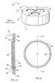
- FIG. 1shows a conventional susceptor 10 that is used in MOCVD reactors such as those provided by Thomas Swan Scientific Equipment Limited. It has a hollowed cylindrical shape and is mounted over the reactor's heating element at the bottom of the reactor, below a source gas inlet. It has a circular base plate 12 and cylindrical sleeve 13 , with the circular plate 12 having a series of circular depressions 14 equally spaced around the susceptor's longitudinal axis. Each of the depressions 14 can hold a semiconductor wafer during growth. When the susceptor 10 is heated by the heating element the semiconductor wafers are also heated and when source gases enter the MOCVD reactor, they combine and deposit on the heated semiconductor wafer as epitaxial layers.
- the susceptor 10can typically spin at speeds in the range of 1,000 to 2,000 rpm, which results in more uniform epitaxial layers on the wafers.
- Conventional susceptors 10are usually formed from a monolithic structure of graphite or coated graphite that absorbs heat from the heater element and conducts it to the wafers in contact with the susceptor 10 .
- the entire susceptor 10is heated uniformly to achieve consistent growth conditions across the entire surface of the wafers.
- materialsnot only deposit on the heated wafer, but can also deposit on the heated susceptor 10 .
- Group III Nitride based devicessignificant amounts of GaN, InGaN, AlInGaN, and similar compounds can deposit on the susceptor surfaces. The result is a buildup of reaction deposits on the susceptor that can adversely impact subsequent fabrication steps.
- the depositscan act as impurities during subsequent growth of the epitaxial layers and they can also result in poor interface transitions between subsequent layers of different compositions. For example, if a layer using an indium source gas is grown on the wafers, indium can be deposited on the susceptor 10 . If the next layer to be grown does not include indium, indium from the susceptor surfaces can be included in the transition between layers and in the next layer. These impurities can cause poor device performance and can prevent consistent reproduction of semiconductor devices on the wafer. This deposition of materials on the susceptor surfaces also results in more reactants being consumed than is necessary for the formation of devices on the wafers.
- MOVPEmetal organic vapor phase epitaxy
- the present inventionseeks to provide an improved apparatus/assembly for mounting a susceptor in an inverted-type reactor for growing semiconductor material on the wafers.
- One embodiment of an apparatus according to the present inventioncomprises a tower having an upper and lower end. The tower's upper end is capable of being mounted to the top inside surface of a reactor chamber. A susceptor is arranged at the tower's lower end. The semiconductor wafers are held adjacent to the susceptor with heat from the susceptor passing to the wafers.
- the present inventionalso discloses a reactor for growing epitaxial layers on semiconductor wafers.
- a reactor according to the present inventioncomprises a reactor chamber with a heating element.
- a susceptoris arranged to transfer heat from the heating element to the semiconductor wafers.
- a meansis included for mounting the susceptor to the top inside surface of the reactor chamber such that heat from the heating element passes into the susceptor.
- a source gas inletis included for gasses to grow epitaxial layers on the semiconductor wafers.
- One embodiment of a susceptor used in the apparatus and reactors according to the present inventioncomprises a base structure made of a material having low thermal conductivity at high temperature to resist transferring heat from the heating element.
- the base structurehas one or more plate holes, each having a respective heat transfer plug arranged within it and a wafer held adjacent to each of the plugs.
- the plugsare made of a material with high thermal conductivity at high temperatures to transfer heat from the reactor's heating element to the wafers.
- FIG. 1is a perspective view of a prior art susceptor
- FIG. 2 ashows a sectional view of one embodiment of a susceptor mounting assembly according to the present invention
- FIGS. 2 b, 2 c and 2 dshow magnified views of features of the susceptor mounting assembly of FIG. 2 a;
- FIGS. 3is a plan view of a base structure for the susceptor mounting assembly of FIG. 2 a;
- FIG. 4is a sectional view of the base structure in FIG. 3, taken along section lines 4 - 4 ;
- FIG. 5is a plan view of a faceplate for the susceptor mounting assembly of FIG. 2 a;
- FIG. 6is a sectional view of the faceplate in FIG. 5, taken along section lines 6 - 6 ;
- FIG. 7is a plan view of a heat transfer plug for the susceptor mounting assembly of FIG. 2 a;
- FIG. 8is a sectional view of the plug in FIG. 7, taken along section lines 8 - 8 ;
- FIG. 9is a sectional view of another embodiment of a susceptor according to the invention that can be used in the susceptor mounting assembly of FIG. 2 a;
- FIG. 10is a sectional view of the wafer holder used in the susceptor of FIG. 9;
- FIG. 11is a sectional view of another embodiment of a susceptor mounting assembly according to the present invention.
- FIG. 12is a plan view of a quartz cup used in the susceptor mounting assembly of FIG. 11;
- FIG. 13is a sectional view of the quartz cup of FIG. 12, taken along section lines 13 - 13 ;
- FIG. 14is a plan view of a quartz tower used in the susceptor mounting assembly of FIG. 11;
- FIG. 15is a sectional view of the quartz tower of FIG. 14, taken along section lines 15 - 15 ;
- FIG. 16is a plan view of a tower retainer used in the susceptor mounting assembly of FIG. 11;
- FIG. 17is an elevation view of the tower retainer in FIG. 16.
- FIG. 18is a simplified diagram of an MOCVD reactor using a susceptor mounting assembly according to the present invention.
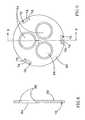
- FIGS. 2 a through 2 dshow one embodiment of a susceptor mounting assembly 40 in accordance with the present invention, that is particularly adapted for use in an inverted type MOCVD reactor wherein the susceptor mounting assembly is mounted to the top of the MOCVD reactor with its wafers facing down.
- the source gassesenter the reactor from below the susceptor mounting assembly to deposit semiconductor materials on the wafers.
- the mounting assembly 40comprises a cylindrical tower, with a susceptor 42 mounted at its lower end 43 .
- the tower's upper end 45is mounted to the top of the MOCVD reactor, over a heater element (not shown).
- the cylindrical tower 44can be made of many different materials but is preferably made of a metal.
- the susceptor 42is mounted at the tower's lower end 43 and comprises a base structure 48 , faceplate 62 , and heat transfer plugs 60 .
- Semiconductor wafers 68are also shown mounted in the susceptor 42 .
- a base structureis shown in FIGS. 3 and 4 and includes a base plate 50 and cylindrical sleeve 52 that can be separate but are preferably combined as one structure.
- the base plate 50has circular plate holes 58 equally spaced around the structure's longitudinal axis.
- the base structure 48has three holes 58 , but different embodiments can have different numbers of holes depending on the number of wafers to be held, the diameter of the wafers and the diameter of the faceplate 50 .
- the base structure 48should be made of a rigid material that has a low thermal conductivity at high temperature so that it transmits minimal heat from the (MOCVD) reactor's heating element. It should also be made of a material that is reflective so that it reflects the heating element's radiative heat to further reduce the amount of heat it transmits. It should also have a low thermal expansion, so that its expansion matches that of the other susceptor components and mounting assembly.
- the base structure 48can be made of many different materials such as boron nitride, fused quartz, aluminum nitride, or a ceramic.
- the aluminum nitride and ceramics embodimentcan be coated with a material to reduce reactance with the source gasses.
- a preferred base structure 48is made of boron nitride or fused quartz covered by boron nitride and can be manufactured using known methods. These materials have high thermal conductivity at low temperature, low thermal conductivity at high temperature, and boron nitride is white, which enhances the structure's reflectivity.
- the outer surface of the sleeve 52has upper and lower axial ridges 68 , 70 (best shown in FIG. 4) that contact the inner surface of the tower 40 . This provides for a space between the majority of the sleeve's outer surface and the tower 40 , which helps reduce the heat transfer between the tower 44 and sleeve 52 .
- the base structure 48can have different diameters depending on the diameter of the tower 44 , with a suitable diameter being approximately 6.2 inches for holding three 2 inch wafers.
- the circular plate 50 and sleeve 52can be different thicknesses, with a suitable thickness being approximately 0.2 inches.
- the base structure 48is arranged within the mounting assembly 40 , with its base plate 50 at the lower end 43 of the tower 44 .
- the lower end 43has an axial lip 54 (best shown in FIGS. 2 b and 2 d ) that holds the base structure 48 within the tower 40 .
- the outside surface of the base plate 50has a depression 56 around its circumference that mates with the axial lip 54 to help secure the base structure 48 as the susceptor mounting assembly 40 rotates during the growth process.
- the faceplate 62is mounted at the lower end 43 of the tower 44 and FIGS. 5 and 6 show one embodiment of a faceplate according to the invention.
- the faceplate 62has through holes 64 arranged to align with the base structure's plate holes 58 .
- Each faceplate hole 64is sized to house a semiconductor wafer 68 and each hole has an axial lip 69 .
- a wafer 68rests on the axial lip and heat transfer plug 60 rests on the wafer 68 (as best shown in FIGS. 2 b and 2 c ).
- the faceplate 62is mounted at the tower's lower end 43 , adjacent to the base structure's circular plate 50 .
- Many different mounting devicescan be used such as clamps, hooks, or screws, with a preferred mounting device being locating pins 66 at the tower's lower end.
- the faceplate 62has three slots 72 equally spaced near its outer edge that are each arranged to mate with a respective locating pin 66 when mounting the faceplate 62 to the tower's lower end 43 .
- the head of each locating pin 66passes through the wider section 74 of its respective axial slot 72 and the faceplate is turned until each slot's narrower section 76 mates with the stem of its locating pin 66 .
- Each slot's narrow section 76also has a counter bore so that when the faceplate 62 is lowered, the head of each locating pin 66 is housed within its respective counter bore.
- the counter boreallows the faceplate 62 to be mounted so that it is not in contact with the tower assembly 44 or the circular plate 50 (to prevent conductive heat transfer) and also secures the faceplate 62 as the tower assembly 40 rotates.
- the faceplate 62provides a surface with a greater resistance to deposition of reaction species, with the surface also being easy to clean. It is preferably infrared transparent so that is does not absorb optical heat. It should also be made of a material that does not react with MOCVD source gasses, such as quartz, pure silicon carbide, sapphire, silicon, coated graphite, graphite or tungsten, with a preferred material being quartz. Deposits can be cleaned from quartz by etching.
- the faceplate 62should have substantially the same diameter as the tower 44 and can be different thicknesses, with a suitable thickness being 0.16 inches.
- the susceptor 42also includes heat transfer plugs 60 , each of which fit within a respective plate hole 58 .
- FIGS. 7 and 8show one embodiment of a heat transfer plug 60 according to the present invention.
- Each plug 60is substantially puck shaped and is designed to transfer heat from the heating element to a semiconductor wafer 68 held in one of the aligned plate holes 58 and faceplate holes 64 .
- Each plug 60rests on a semiconductor wafers and during growth of the epitaxial layers heat from the heating element is conducted through each plug 60 , to its wafer 68 .
- the plugs 32are preferably made of a material having high thermal conductivity at high temperature and a dark color, both of which promote heat conduction.
- the preferred material for the plugs 32is graphite or silicon carbide coated graphite.
- Each plug 60can has a ridge 78 that forms a circle on the plug's surface adjacent to the wafer 68 , with only the rib 78 contacting the wafer 68 (as best shown in FIGS. 2 b and 2 c ). This provides a space between the wafer 68 and the plug 60 to promote even convective heating of the wafer 68 .
- the surface of the plug 60 that is adjacent to the wafer 68can be convex, concave, or have other shapes.
- Each of the plugsis manufactured separately from the remainder of the susceptor so that the surfaces are easier to shape compared to shaping the surfaces in a conventional monolithic structure of graphite.
- the plug 60should have a diameter that allows it to fit closely within the circular plate and faceplate holes 58 , 64 and can have many different thicknesses, with a suitable thickness being approximately 0.33 inches.
- the rib 78can be many different sizes and shapes, with a suitable size being 0.002 inches high and 0.003 inches wide. It should also be understood that the ridge can form shapes other than a circle, such as a square, rectangle, triangle or hexagon.
- the heating elementWhen the susceptor assembly 40 is mounted from the top of an MOCVD reactor, over the reactor's heating element, the heating element is in close proximity to the susceptor 42 , such that most of the heat interacts with the susceptor 42 .
- the base structure 48is made of a material that resists heat transfer and the plugs 60 are made of a material that promotes heat transfer. This arrangement results in most of the heat transferring to the plugs 60 and on to its adjacent wafer 68 .
- the heat transfer into the base structureis minimized, which minimizes wasted heat and reduces the heating of the faceplate 62 . This results in the minimization of reactants that are deposited on the faceplate 62 during growth of the epitaxial layers.
- the wafers 68are mounted in the susceptor mounting assembly 40 before growth of the epitaxial layers, by placing the wafers 68 and transfer plugs 60 in the faceplate holes 64 .
- the faceplate 62is then positioned at the tower's lower end 43 with its holes 64 aligned with the base structure's holes 58 .
- the locating pins 66are then mated to the axial slots 72 , to mount the faceplate 62 to the tower 44 .
- the wafers 68are uncovered by the faceplate 62 and when the plugs 60 are heated by the heating element, the wafers 68 are also heated.
- the susceptor assemblyis typically rotated and source gasses are fed into the reactor to grow epitaxial layers on the wafers 68 .
- the tower 44has a series of adjustment holes 79 near its upper end 45 that are used to attach the susceptor assembly 40 to the top of the reactor. By using different holes, the level at which the wafers are held can be adjusted.
- the growth gassescan enter the reactor through a “shower head” (not shown) that is mounted at the bottom of the reactor and is directed toward the wafers. By using different adjustment holes, the distance between the wafers 68 and the “shower head” can be adjusted, which can impact the growth characteristics of the epitaxial layers.
- FIGS. 9shows another embodiment of a susceptor 80 in accordance with the present invention that is similar to the susceptor 42 above. It has a similar base structure circular plate 81 and faceplate 83 that have aligned holes and can be made of similar material to the corresponding parts in susceptor 42 .
- a wafer 84 and plug 86are arranged in the aligned plate and faceplate holes and function in much the same way as the wafer 68 and plug 60 in the susceptor 42 .
- a wafer holder 88is included that provides a lip for holding the wafer 84 and plug 86 .
- each circular plate hole 90has a lower ledge 92 on its inner surface, and each of the faceplate holes 94 do not have a lip.
- Each wafer holder 82has an axial ridge 96 on its outer surface that rests on a ledge 92 to hold the wafer holder 88 in its respective hole 90 .
- Each wafer holder 88also has an internal lip 98 on which the wafer 84 rests and the plug 86 rests on the wafer 84 , with both being arranged within the wafer holder 88 .
- each wafer holder 88protrudes from the circular plate 81 , and when the faceplate 83 is mounted on the tower 44 (as described above), the lower portion 97 is within the faceplate hole 94 .
- Each wafer holder 88can be made of many different materials, with a suitable material being graphite or silicon carbide coated graphite.
- the faceplate 83is preferably made of quartz, which can be difficult and costly to machine. For example, when machining fine features such as a hole lip, the quartz can be damaged beyond repair and the faceplate rendered unusable. Also, it is difficult to machine small features in quartz and the lip thickness is limited to approximately 0.025 inches (graphite has a limit of 0.010 inches).
- One advantage of the susceptor 80is that each of the faceplate holes 92 do not need to be machined to have a lip. This avoids the costs associated with the fine machining and avoids the waste of damaged faceplates.
- the lower surface of the wafer holder 88can be exposed to the epitaxial growth process. This can result in graphite impurities being introduced into the growth process and can result in reactants being deposited on the graphite surface. These deposits can act as impurities that lead to pre-reaction in the growth of subsequent layers.
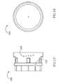
- FIG. 11shows another embodiment of a susceptor mounting assembly 100 according to the present invention adapted for use in an inverted type MOCVD reactor, with the majority of the assembly 100 being made of quartz.
- the assembly 100includes a metal tower retainer 102 , which serves as a mounting point between the top of the MOCVD reactor and the remainder of the assembly 100 .
- the tower retainer 102is mounted to the upper end 103 of a cylindrical quartz tower 104 , and a quartz cup 106 is mounted to the tower's lower end 108 .
- a susceptor 110is housed within the quartz cup 106 at the tower's lower end 108 .
- the susceptor 110has a base structure 112 similar to the base structure 42 shown in FIGS. 3 and 4 above and includes a circular plate 114 and a sleeve 116 .
- the structure 42is similarly made of a material that resists heat transfer.
- the circular plate 114has holes 118 for heat transfer plugs 120 , with the holes equally spaced around the base structure's longitudinal axis.
- FIGS. 12 and 13show the quartz cup 106 , which has a base 122 with holes 124 that align with the plate holes 114 , with each of the base holes 124 having a lip 126 to hold a wafer 128 .
- a heat transfer plug 120similar to the plug 60 shown above in FIGS. 7 and 8, then rests on the wafer 128 .
- the plug 120should similarly be made of a material that promotes heat transfer from the heating element.
- the base plate 114is positioned adjacent to the cup base 122 and the plate 114 has a ridge 130 around the circumference of its surface adjacent the cup base 122 .
- This ridge 130allows for a space between the base plate 114 and cup base 122 to reduce conductive heat transfer.
- the sleeve 116also has two axial ridges 132 and 134 that allow for a space between the sleeve 132 and the cup 106 , which reduces conductive heat transfer between the two.
- the quartz cup 106has three equally spaced J-slots 134 that provide a means for mounting the cup 106 to the tower 104 , although other mounting methods could also be used.
- the cup 106also includes three equally spaced pin grooves 136 for pins that secure the quartz cup 106 to the tower 104 .
- the quartz cup 106 and susceptor 116can also be arranged to support the wafer holder embodiment (not shown) as described above in FIGS. 10 and 11.
- each of the holes in the circular platehas ledge and the exterior ridge on each of the wafer holders is arranged to rest on the one of the ledges.
- the wafer holderhas a lower lip that holds a wafer and a heat transfer plug rests on the wafer.
- each waferrest on a lip 126 on the inner surface of each hole in the cup base 122 , and the heat transfer plug rests on the wafer.
- the wafersare substantially uncovered by the cup's base 122 so that growth gasses can deposit epitaxial layers on the wafers.
- FIGS. 14 and 15show one embodiment of a quartz tower 104 according to the invention, which has a slightly smaller diameter than the quartz cup 106 .
- the tower 104has three pins 138 on the outside surface of its lower end 108 , for mating with the quartz cup's J-slots 134 .
- the quartz cup 106slides onto the end 108 of the quartz tower 104 and the pins 138 slide into the J-slots 134 .
- the cup 106is then turned until each of the pins 138 rests in the axial sections 140 of the J-slots 134 .
- the tower 104also has longitudinal grooves 146 , which align with the pin grooves 136 in the quartz cup 106 .
- the aligned grooves 136 , 146provide holes into which pins can be inserted to secure the quartz cup to the tower 104 to prevent the cup from turning off the tower pins 138 as the susceptor assembly 100 rotates.
- the tower shell 104also has three equally spaced mounting holes 144 used to secure the tube retainer 102 to the tower 104 .
- FIGS. 16 and 17show the quartz tower retainer 102 , which mounts to the upper end 103 of the tower shell 104 .
- the tower retainer 102has mounting holes 150 that align with the tower holes 144 . Pins or screws can be inserted into the aligned holes 144 , 150 to mount the tube retainer 102 to the tower 104 .
- the tower retainer 102has a series of adjustment holes 152 that are used to attach the susceptor assembly 100 to the top of the reactor. By using different holes, the distance between the wafers and the source gas inlet (shower head) can be adjusted, which can change the growth characteristics of the epitaxial layers.
- the tower 104 and retainer 102 combinationare mounted to the top inside surface of the reactor chamber, over the heating element.
- the wafers 128are then placed into the quartz cup holes 124 .
- the base structure 112 and plugs 120are then arranged in the cup 106 and the cup 106 is mounted to the tower 104 .
- the mounting of wafer 128 in the assembly 100can be more reliable compared to mounting wafers in the faceplate 62 arrangement in the susceptor assembly 40 above.
- the faceplate 62can be more difficult to handle and deposits on the faceplate 62 can interfere with the mating of the locating pins 66 within the slots 72 .
- the susceptor assembly 100uses less power during growth because the quartz components 104 , 106 absorb less of the heat compared to the metal tower 44 . Quartz is also easier to clean compared to the metal tower 44 , with one of the cleaning methods being etching. However, the assembly 100 is more expansive to manufacture and the quartz tower 104 may be limited to certain diameters when using standard tube sizes.
- FIG. 18shows one embodiment of an MOCVD reactor 160 that can utilize a susceptor mounting assembly in accordance with the present invention.
- the reactor 160comprises a reaction chamber 162 having a rotatable susceptor mounting assembly 164 mounted to the top inside surface.
- One or more wafersare mounted in the susceptor mounting assembly, in the faceplate 165 .
- the waferscan be mounted differently for other susceptor mounting assembly embodiments.
- the susceptor mounting assembly 164is heated by a heater element (not shown) that is arranged within the susceptor mounting assembly 164 , adjacent to the wafers.
- the heating elementcan be a variety of heating devices but is usually a radio frequency (RF) coil, resistance coil, or a strip heater.
- RFradio frequency
- a carrier gas 166is supplied to a gas line 168 , the carrier gas being an inert gas such as hydrogen or nitrogen.
- the carrier gas 166is also supplied through mass flow controllers 170 a, 170 b, 170 c to respective bubblers 172 a, 172 b, 172 c.
- Bubbler 172 acan have a growth compound, such as an alkylated compound having a methyl group, e.g. trimethyl gallium (TMG), trimethyl aluminum (TMA) or timethyl indium (TMI).
- Bubbler 172 b and 172 cmay also contain a similar methyl group compound to be able to grow an alloy of a Group III compound.
- the bubblers 172 a, 172 b, 172 care typically maintained at a predetermined temperature by constant temperature baths 174 a, 174 b, 174 c to ensure a constant vapor pressure of the metal organic compound before it is carried to the reaction chamber 162 by the carrier gas 166 .
- the carrier gas 166which passes through bubblers 172 a, 172 b, 172 c is mixed with the carrier gas 166 flowing within the gas line 168 by opening the desired combination of valves 176 a, 176 b, 176 c.
- the mixed gasis then introduced into the reaction chamber 162 through a gas inlet port 178 formed at the upper end of the reaction chamber 162 .
- a shower head inlet(not shown) can be included at the inlet port 178 .
- a nitrogen containing gas 180such as ammonia
- a nitrogen containing gas 180is supplied to the gas line 168 through a mass flow controller 182 and the flow of nitrogen containing gas is controlled by valve 184 . If the carrier gas 166 is mixed with the nitrogen containing gas 180 and the TMG vapor within the gas line 168 and then introduced into the reaction chamber 162 , the elements are present to grow gallium nitride on the wafer through thermal decomposition of the molecules present in the TMG and ammonia containing gas.
- one of the bubblers 172 a, 172 b, 172 c not being used for the TMGis used for a dopant material, which is usually Magnesium (Mg) or Silicon (Si), but can be other material such as beryllium, calcium, zinc, or carbon.
- Bubbler 172 b or 172 ccan be used for an alloy material such as boron aluminum, indium, phosphorous, arsenic or other materials.
- valves 176 a, 176 b, 176 cis opened to allow the dopant to flow into gas line 168 with the gallium and nitrogen containing gas 180 , the growth of the doped layer of gallium nitride takes place on the wafer.
- the gas within the reaction chamber 162can be purged through a gas purge line 186 connected to a pump 188 operable under hydraulic pressure. Further, a purge valve 190 allows gas pressure to build up or be bled off from the reaction chamber 162 .
- the growth processis typically stopped by shutting off the gallium and dopant sources by closing valves 176 a and 176 b, and keeping the nitrogen containing gas and the carrier gas flowing.
- the reaction chamber 162can be purged with a gas 190 that can be controlled through a mass flow controller 192 and valve 194 .
- the purgeis aided by opening valve 190 to allow the pump 188 to evacuate the reaction chamber 162 of excess growth gasses.
- the purge gas 190is hydrogen, but can be other gasses.
- the wafersare then cooled by turning off power to the heater element.
- the present inventionhas been described in considerable detail with reference to certain preferred configurations thereof, other versions are possible.
- the new susceptorcan be used in many different reactors beyond MOCVD reactors and can be used in many different types of MOCVD reactors.
- the new susceptors and susceptor assembliescan be made of many different materials with many different dimensions. Therefore, the spirit and scope of the appended claims should not be limited to the preferred versions in the specification.
Landscapes
- Chemical & Material Sciences (AREA)
- General Chemical & Material Sciences (AREA)
- Chemical Kinetics & Catalysis (AREA)
- Engineering & Computer Science (AREA)
- Materials Engineering (AREA)
- Metallurgy (AREA)
- Organic Chemistry (AREA)
- Mechanical Engineering (AREA)
- Crystallography & Structural Chemistry (AREA)
Abstract
Description
- 1. Field of the Invention[0001]
- This invention relates to Metalorganic Chemical Vapor Deposition (MOCVD) reactors and more particularly to susceptors used in MOCVD reactors.[0002]
- 2. Description of the Related Art[0003]
- Fabrication of gallium nitride (GaN) based semiconductor devices in MOCVD reactors is generally described in DenBaars and Keller,[0004]Semiconductors and Semimetals, Vol. 50, Academic Press Inc., 1997, p. 11-35. MOCVD is a nonequilibrium growth technique that relies on vapor transport of the precursers and subsequent reactions of group III alkyls and group V hydrides in a heated zone. Growth/source gasses and dopants are supplied to the reactor and are deposited as epitaxial layers on a substrate or wafer. One or more wafers usually rest on a structure of graphite called a susceptor that is heated by a heating element such as a radio frequency (RF) coil, resistance heated, or radiantly heated by a strip heater. The heated susceptor then heats the wafers, which allows for the source gasses to form epitaxial layers on the wafers.
- FIG. 1 shows a[0005]
conventional susceptor 10 that is used in MOCVD reactors such as those provided by Thomas Swan Scientific Equipment Limited. It has a hollowed cylindrical shape and is mounted over the reactor's heating element at the bottom of the reactor, below a source gas inlet. It has acircular base plate 12 andcylindrical sleeve 13, with thecircular plate 12 having a series ofcircular depressions 14 equally spaced around the susceptor's longitudinal axis. Each of thedepressions 14 can hold a semiconductor wafer during growth. When thesusceptor 10 is heated by the heating element the semiconductor wafers are also heated and when source gases enter the MOCVD reactor, they combine and deposit on the heated semiconductor wafer as epitaxial layers. Thesusceptor 10 can typically spin at speeds in the range of 1,000 to 2,000 rpm, which results in more uniform epitaxial layers on the wafers. - [0006]
Conventional susceptors 10 are usually formed from a monolithic structure of graphite or coated graphite that absorbs heat from the heater element and conducts it to the wafers in contact with thesusceptor 10. Theentire susceptor 10 is heated uniformly to achieve consistent growth conditions across the entire surface of the wafers. However, during fabrication of the epitaxial layers, materials not only deposit on the heated wafer, but can also deposit on theheated susceptor 10. For example, during growth of Group III Nitride based devices, significant amounts of GaN, InGaN, AlInGaN, and similar compounds can deposit on the susceptor surfaces. The result is a buildup of reaction deposits on the susceptor that can adversely impact subsequent fabrication steps. The deposits can act as impurities during subsequent growth of the epitaxial layers and they can also result in poor interface transitions between subsequent layers of different compositions. For example, if a layer using an indium source gas is grown on the wafers, indium can be deposited on thesusceptor 10. If the next layer to be grown does not include indium, indium from the susceptor surfaces can be included in the transition between layers and in the next layer. These impurities can cause poor device performance and can prevent consistent reproduction of semiconductor devices on the wafer. This deposition of materials on the susceptor surfaces also results in more reactants being consumed than is necessary for the formation of devices on the wafers. - Another disadvantage of conventional susceptors is that because the heating element heats the entire susceptor (not just the areas under or around the wafers) large amounts of heat are required. Conventional susceptors have a relatively large surface area in comparison to the wafers and most of the energy is wasted by not heating the wafers. This taxes the heater, contributing to early heater failures.[0007]
- Another disadvantage of conventional susceptors is that they are difficult to manufacture. They are machined from a large section of graphite and if any part of the susceptor is damaged the entire structure can be unusable. The fabrication of the depressions can be extremely difficult because they are offset from the structure's longitudinal axis and as a result, they cannot be machined using a simple lathe, but must involve more complex processes. In some susceptors it may also be desirable to shape the surface of the depressions to compensate for variations in temperature. For the same reasons that it is difficult to machine the depressions, it also difficult to shape the surface of the depressions.[0008]
- Various “inverted” type systems have been developed to grow semiconductor devices, wherein the susceptor is not mounted at the bottom of the reactor. An inverted type metal organic vapor phase epitaxy (MOVPE) system for the growth of Group III-V compound semiconductor materials is described in Aria et al.,[0009]Highly Uniform Growth on a Low-Pressure MOPVE Multiple Wafer System, Journal of Crystal Growth 170, Pgs. 88-91 (1997). The wafers are held in a susceptor and placed facedown (inverted) in the growth chamber, with the flow gasses flowing under the growth surfaces. Gasses are injected into the chamber from one of the sidewalls of the chamber, through a triple flow channel, and the gas exhaust is on the opposite sidewall.
- The fluid flow and mass transport for “chimney” chemical vapor deposition (CVD) reactors is discussed in Holstein,[0010]Modeling of Chimney CVD Reactors, Journal of Crystal Growth 125, Pgs. 311-319 (1992). A chimney reactor has wafers held on heated susceptors (usually two) that are vertically mounted on the interior side walls of the reactor.
- Growth of GaAs based semiconductor devices in an MOCVD reactor is also discussed in Lee et al.[0011]MOCVD in Inverted Stagnation Point Flow, Journal of Crystal Growth, Pgs 120-127 (1886). The reactor is based on inverted stagnation point flow geometry where the reactants flow up towards wafers clamped to an inverted heated susceptor.
- Each of these inverted type systems use conventional susceptors that are usually formed from a monolithic structure of graphite or coated graphite. They also suffer from the disadvantages described above.[0012]
- The present invention seeks to provide an improved apparatus/assembly for mounting a susceptor in an inverted-type reactor for growing semiconductor material on the wafers. One embodiment of an apparatus according to the present invention comprises a tower having an upper and lower end. The tower's upper end is capable of being mounted to the top inside surface of a reactor chamber. A susceptor is arranged at the tower's lower end. The semiconductor wafers are held adjacent to the susceptor with heat from the susceptor passing to the wafers.[0013]
- The present invention also discloses a reactor for growing epitaxial layers on semiconductor wafers. One embodiment of a reactor according to the present invention comprises a reactor chamber with a heating element. A susceptor is arranged to transfer heat from the heating element to the semiconductor wafers. A means is included for mounting the susceptor to the top inside surface of the reactor chamber such that heat from the heating element passes into the susceptor. A source gas inlet is included for gasses to grow epitaxial layers on the semiconductor wafers.[0014]
- One embodiment of a susceptor used in the apparatus and reactors according to the present invention comprises a base structure made of a material having low thermal conductivity at high temperature to resist transferring heat from the heating element. The base structure has one or more plate holes, each having a respective heat transfer plug arranged within it and a wafer held adjacent to each of the plugs. The plugs are made of a material with high thermal conductivity at high temperatures to transfer heat from the reactor's heating element to the wafers.[0015]
- These and other features and advantages of the invention will be apparent to those skilled in the art from the following detailed description, taken together with the accompanying drawings, in which:[0016]
- FIG. 1 is a perspective view of a prior art susceptor;[0017]
- FIG. 2[0018]ashows a sectional view of one embodiment of a susceptor mounting assembly according to the present invention;
- FIGS. 2[0019]b,2cand2dshow magnified views of features of the susceptor mounting assembly of FIG. 2a;
- FIGS.[0020]3 is a plan view of a base structure for the susceptor mounting assembly of FIG. 2a;
- FIG. 4 is a sectional view of the base structure in FIG. 3, taken along section lines[0021]4-4;
- FIG. 5 is a plan view of a faceplate for the susceptor mounting assembly of FIG. 2[0022]a;
- FIG. 6 is a sectional view of the faceplate in FIG. 5, taken along section lines[0023]6-6;
- FIG. 7 is a plan view of a heat transfer plug for the susceptor mounting assembly of FIG. 2[0024]a;
- FIG. 8 is a sectional view of the plug in FIG. 7, taken along section lines[0025]8-8;
- FIG. 9 is a sectional view of another embodiment of a susceptor according to the invention that can be used in the susceptor mounting assembly of FIG. 2[0026]a;
- FIG. 10 is a sectional view of the wafer holder used in the susceptor of FIG. 9;[0027]
- FIG. 11 is a sectional view of another embodiment of a susceptor mounting assembly according to the present invention;[0028]
- FIG. 12 is a plan view of a quartz cup used in the susceptor mounting assembly of FIG. 11;[0029]
- FIG. 13 is a sectional view of the quartz cup of FIG. 12, taken along section lines[0030]13-13;
- FIG. 14 is a plan view of a quartz tower used in the susceptor mounting assembly of FIG. 11;[0031]
- FIG. 15 is a sectional view of the quartz tower of FIG. 14, taken along section lines[0032]15-15;
- FIG. 16 is a plan view of a tower retainer used in the susceptor mounting assembly of FIG. 11;[0033]
- FIG. 17 is an elevation view of the tower retainer in FIG. 16; and[0034]
- FIG. 18 is a simplified diagram of an MOCVD reactor using a susceptor mounting assembly according to the present invention.[0035]
- FIGS. 2[0036]athrough2dshow one embodiment of a
susceptor mounting assembly 40 in accordance with the present invention, that is particularly adapted for use in an inverted type MOCVD reactor wherein the susceptor mounting assembly is mounted to the top of the MOCVD reactor with its wafers facing down. The source gasses enter the reactor from below the susceptor mounting assembly to deposit semiconductor materials on the wafers. - The mounting[0037]
assembly 40 comprises a cylindrical tower, with asusceptor 42 mounted at itslower end 43. The tower'supper end 45 is mounted to the top of the MOCVD reactor, over a heater element (not shown). Thecylindrical tower 44 can be made of many different materials but is preferably made of a metal. - The[0038]
susceptor 42 is mounted at the tower'slower end 43 and comprises abase structure 48,faceplate 62, and heat transfer plugs60.Semiconductor wafers 68 are also shown mounted in thesusceptor 42. One embodiment of a base structure is shown in FIGS. 3 and 4 and includes abase plate 50 andcylindrical sleeve 52 that can be separate but are preferably combined as one structure. Thebase plate 50 has circular plate holes58 equally spaced around the structure's longitudinal axis. Thebase structure 48 has threeholes 58, but different embodiments can have different numbers of holes depending on the number of wafers to be held, the diameter of the wafers and the diameter of thefaceplate 50. - The[0039]
base structure 48 should be made of a rigid material that has a low thermal conductivity at high temperature so that it transmits minimal heat from the (MOCVD) reactor's heating element. It should also be made of a material that is reflective so that it reflects the heating element's radiative heat to further reduce the amount of heat it transmits. It should also have a low thermal expansion, so that its expansion matches that of the other susceptor components and mounting assembly. - The[0040]
base structure 48 can be made of many different materials such as boron nitride, fused quartz, aluminum nitride, or a ceramic. The aluminum nitride and ceramics embodiment can be coated with a material to reduce reactance with the source gasses. Apreferred base structure 48 is made of boron nitride or fused quartz covered by boron nitride and can be manufactured using known methods. These materials have high thermal conductivity at low temperature, low thermal conductivity at high temperature, and boron nitride is white, which enhances the structure's reflectivity. - The outer surface of the[0041]
sleeve 52 has upper and loweraxial ridges 68,70 (best shown in FIG. 4) that contact the inner surface of thetower 40. This provides for a space between the majority of the sleeve's outer surface and thetower 40, which helps reduce the heat transfer between thetower 44 andsleeve 52. - The[0042]
base structure 48 can have different diameters depending on the diameter of thetower 44, with a suitable diameter being approximately 6.2 inches for holding three 2 inch wafers. Thecircular plate 50 andsleeve 52 can be different thicknesses, with a suitable thickness being approximately 0.2 inches. - Referring again to FIG. 2[0043]a,the
base structure 48 is arranged within the mountingassembly 40, with itsbase plate 50 at thelower end 43 of thetower 44. Thelower end 43 has an axial lip54 (best shown in FIGS. 2band2d) that holds thebase structure 48 within thetower 40. The outside surface of thebase plate 50 has adepression 56 around its circumference that mates with theaxial lip 54 to help secure thebase structure 48 as thesusceptor mounting assembly 40 rotates during the growth process. - The[0044]
faceplate 62 is mounted at thelower end 43 of thetower 44 and FIGS. 5 and 6 show one embodiment of a faceplate according to the invention. Thefaceplate 62 has throughholes 64 arranged to align with the base structure's plate holes58. Eachfaceplate hole 64 is sized to house asemiconductor wafer 68 and each hole has anaxial lip 69. Awafer 68 rests on the axial lip andheat transfer plug 60 rests on the wafer68 (as best shown in FIGS. 2band2c). - Referring again to FIG. 2[0045]a,the
faceplate 62 is mounted at the tower'slower end 43, adjacent to the base structure'scircular plate 50. Many different mounting devices can be used such as clamps, hooks, or screws, with a preferred mounting device being locatingpins 66 at the tower's lower end. Thefaceplate 62 has threeslots 72 equally spaced near its outer edge that are each arranged to mate with arespective locating pin 66 when mounting thefaceplate 62 to the tower'slower end 43. The head of each locatingpin 66 passes through thewider section 74 of its respectiveaxial slot 72 and the faceplate is turned until each slot'snarrower section 76 mates with the stem of its locatingpin 66. Each slot'snarrow section 76 also has a counter bore so that when thefaceplate 62 is lowered, the head of each locatingpin 66 is housed within its respective counter bore. The counter bore allows thefaceplate 62 to be mounted so that it is not in contact with thetower assembly 44 or the circular plate50 (to prevent conductive heat transfer) and also secures thefaceplate 62 as thetower assembly 40 rotates. - Small amounts of reactants can deposit on the[0046]
base structure 48 during epitaxial growth. Thefaceplate 62 provides a surface with a greater resistance to deposition of reaction species, with the surface also being easy to clean. It is preferably infrared transparent so that is does not absorb optical heat. It should also be made of a material that does not react with MOCVD source gasses, such as quartz, pure silicon carbide, sapphire, silicon, coated graphite, graphite or tungsten, with a preferred material being quartz. Deposits can be cleaned from quartz by etching. Thefaceplate 62 should have substantially the same diameter as thetower 44 and can be different thicknesses, with a suitable thickness being 0.16 inches. - Referring again to FIG. 2[0047]a,the
susceptor 42 also includes heat transfer plugs60, each of which fit within arespective plate hole 58. FIGS. 7 and 8 show one embodiment of a heat transfer plug60 according to the present invention. Eachplug 60 is substantially puck shaped and is designed to transfer heat from the heating element to asemiconductor wafer 68 held in one of the aligned plate holes58 and faceplate holes64. Eachplug 60 rests on a semiconductor wafers and during growth of the epitaxial layers heat from the heating element is conducted through eachplug 60, to itswafer 68. The plugs32 are preferably made of a material having high thermal conductivity at high temperature and a dark color, both of which promote heat conduction. The preferred material for the plugs32 is graphite or silicon carbide coated graphite. - Each[0048]
plug 60 can has aridge 78 that forms a circle on the plug's surface adjacent to thewafer 68, with only therib 78 contacting the wafer68 (as best shown in FIGS. 2band2c). This provides a space between thewafer 68 and theplug 60 to promote even convective heating of thewafer 68. To further promote even heating of thewafer 68, the surface of theplug 60 that is adjacent to thewafer 68 can be convex, concave, or have other shapes. Each of the plugs is manufactured separately from the remainder of the susceptor so that the surfaces are easier to shape compared to shaping the surfaces in a conventional monolithic structure of graphite. - The[0049]
plug 60 should have a diameter that allows it to fit closely within the circular plate and faceplate holes58,64 and can have many different thicknesses, with a suitable thickness being approximately 0.33 inches. Therib 78 can be many different sizes and shapes, with a suitable size being 0.002 inches high and 0.003 inches wide. It should also be understood that the ridge can form shapes other than a circle, such as a square, rectangle, triangle or hexagon. - When the[0050]
susceptor assembly 40 is mounted from the top of an MOCVD reactor, over the reactor's heating element, the heating element is in close proximity to thesusceptor 42, such that most of the heat interacts with thesusceptor 42. Thebase structure 48 is made of a material that resists heat transfer and theplugs 60 are made of a material that promotes heat transfer. This arrangement results in most of the heat transferring to theplugs 60 and on to itsadjacent wafer 68. The heat transfer into the base structure is minimized, which minimizes wasted heat and reduces the heating of thefaceplate 62. This results in the minimization of reactants that are deposited on thefaceplate 62 during growth of the epitaxial layers. By having the heating element within thesusceptor 42, the amount of heat that passes into thetower 44 is also minimized. - The[0051]
wafers 68 are mounted in thesusceptor mounting assembly 40 before growth of the epitaxial layers, by placing thewafers 68 and transfer plugs60 in the faceplate holes64. Thefaceplate 62 is then positioned at the tower'slower end 43 with itsholes 64 aligned with the base structure'sholes 58. The locating pins66 are then mated to theaxial slots 72, to mount thefaceplate 62 to thetower 44. Thewafers 68 are uncovered by thefaceplate 62 and when theplugs 60 are heated by the heating element, thewafers 68 are also heated. The susceptor assembly is typically rotated and source gasses are fed into the reactor to grow epitaxial layers on thewafers 68. - The[0052]
tower 44 has a series of adjustment holes79 near itsupper end 45 that are used to attach thesusceptor assembly 40 to the top of the reactor. By using different holes, the level at which the wafers are held can be adjusted. In one inverted MOCVD reactor, the growth gasses can enter the reactor through a “shower head” (not shown) that is mounted at the bottom of the reactor and is directed toward the wafers. By using different adjustment holes, the distance between thewafers 68 and the “shower head” can be adjusted, which can impact the growth characteristics of the epitaxial layers. - FIGS.[0053]9 shows another embodiment of a
susceptor 80 in accordance with the present invention that is similar to thesusceptor 42 above. It has a similar base structurecircular plate 81 andfaceplate 83 that have aligned holes and can be made of similar material to the corresponding parts insusceptor 42. Awafer 84 and plug86 are arranged in the aligned plate and faceplate holes and function in much the same way as thewafer 68 and plug60 in thesusceptor 42. However, instead of eachwafer 68 and plug resting on a faceplate hole lip (as above), awafer holder 88 is included that provides a lip for holding thewafer 84 and plug86. In this embodiment eachcircular plate hole 90 has alower ledge 92 on its inner surface, and each of the faceplate holes94 do not have a lip. Each wafer holder82 has anaxial ridge 96 on its outer surface that rests on aledge 92 to hold thewafer holder 88 in itsrespective hole 90. Eachwafer holder 88 also has aninternal lip 98 on which thewafer 84 rests and theplug 86 rests on thewafer 84, with both being arranged within thewafer holder 88. - The[0054]
lower portion 97 of eachwafer holder 88 protrudes from thecircular plate 81, and when thefaceplate 83 is mounted on the tower44 (as described above), thelower portion 97 is within thefaceplate hole 94. Eachwafer holder 88 can be made of many different materials, with a suitable material being graphite or silicon carbide coated graphite. - As described above, the[0055]
faceplate 83 is preferably made of quartz, which can be difficult and costly to machine. For example, when machining fine features such as a hole lip, the quartz can be damaged beyond repair and the faceplate rendered unusable. Also, it is difficult to machine small features in quartz and the lip thickness is limited to approximately 0.025 inches (graphite has a limit of 0.010 inches). One advantage of thesusceptor 80 is that each of the faceplate holes92 do not need to be machined to have a lip. This avoids the costs associated with the fine machining and avoids the waste of damaged faceplates. However, when using thesusceptor 80 during growth, the lower surface of thewafer holder 88 can be exposed to the epitaxial growth process. This can result in graphite impurities being introduced into the growth process and can result in reactants being deposited on the graphite surface. These deposits can act as impurities that lead to pre-reaction in the growth of subsequent layers. - FIG. 11 shows another embodiment of a[0056]
susceptor mounting assembly 100 according to the present invention adapted for use in an inverted type MOCVD reactor, with the majority of theassembly 100 being made of quartz. Theassembly 100 includes ametal tower retainer 102, which serves as a mounting point between the top of the MOCVD reactor and the remainder of theassembly 100. Thetower retainer 102 is mounted to theupper end 103 of acylindrical quartz tower 104, and aquartz cup 106 is mounted to the tower'slower end 108. Asusceptor 110, according to the present invention, is housed within thequartz cup 106 at the tower'slower end 108. - The[0057]
susceptor 110 has abase structure 112 similar to thebase structure 42 shown in FIGS. 3 and 4 above and includes acircular plate 114 and asleeve 116. Thestructure 42 is similarly made of a material that resists heat transfer. Thecircular plate 114 hasholes 118 for heat transfer plugs120, with the holes equally spaced around the base structure's longitudinal axis. FIGS. 12 and 13 show thequartz cup 106, which has a base122 withholes 124 that align with the plate holes114, with each of the base holes124 having alip 126 to hold awafer 128. Aheat transfer plug 120 similar to theplug 60 shown above in FIGS. 7 and 8, then rests on thewafer 128. Theplug 120 should similarly be made of a material that promotes heat transfer from the heating element. - Referring to FIG. 11, the[0058]
base plate 114 is positioned adjacent to thecup base 122 and theplate 114 has aridge 130 around the circumference of its surface adjacent thecup base 122. Thisridge 130 allows for a space between thebase plate 114 andcup base 122 to reduce conductive heat transfer. Thesleeve 116 also has twoaxial ridges sleeve 132 and thecup 106, which reduces conductive heat transfer between the two. - Referring again to FIGS. 12 and 13, the[0059]
quartz cup 106 has three equally spaced J-slots 134 that provide a means for mounting thecup 106 to thetower 104, although other mounting methods could also be used. Thecup 106 also includes three equally spacedpin grooves 136 for pins that secure thequartz cup 106 to thetower 104. - The[0060]
quartz cup 106 andsusceptor 116 can also be arranged to support the wafer holder embodiment (not shown) as described above in FIGS. 10 and 11. For the wafer holder embodiment, each of the holes in the circular plate has ledge and the exterior ridge on each of the wafer holders is arranged to rest on the one of the ledges. The wafer holder has a lower lip that holds a wafer and a heat transfer plug rests on the wafer. - For the embodiment shown in FIGS. 12 and 13, each wafer rest on a[0061]
lip 126 on the inner surface of each hole in thecup base 122, and the heat transfer plug rests on the wafer. In this and the wafer holder embodiment, the wafers are substantially uncovered by the cup's base122 so that growth gasses can deposit epitaxial layers on the wafers. - FIGS. 14 and 15 show one embodiment of a[0062]
quartz tower 104 according to the invention, which has a slightly smaller diameter than thequartz cup 106. Thetower 104 has threepins 138 on the outside surface of itslower end 108, for mating with the quartz cup's J-slots 134. Thequartz cup 106 slides onto theend 108 of thequartz tower 104 and thepins 138 slide into the J-slots 134. Thecup 106 is then turned until each of thepins 138 rests in theaxial sections 140 of the J-slots 134. Thetower 104 also haslongitudinal grooves 146, which align with thepin grooves 136 in thequartz cup 106. The alignedgrooves tower 104 to prevent the cup from turning off the tower pins138 as thesusceptor assembly 100 rotates. Thetower shell 104 also has three equally spaced mountingholes 144 used to secure thetube retainer 102 to thetower 104. - FIGS. 16 and 17 show the[0063]
quartz tower retainer 102, which mounts to theupper end 103 of thetower shell 104. Thetower retainer 102 has mountingholes 150 that align with the tower holes144. Pins or screws can be inserted into the alignedholes tube retainer 102 to thetower 104. - The[0064]
tower retainer 102 has a series of adjustment holes152 that are used to attach thesusceptor assembly 100 to the top of the reactor. By using different holes, the distance between the wafers and the source gas inlet (shower head) can be adjusted, which can change the growth characteristics of the epitaxial layers. - To mount the[0065]
wafers 128 into an MOCVD reactor using theassembly 100, thetower 104 andretainer 102 combination are mounted to the top inside surface of the reactor chamber, over the heating element. Thewafers 128 are then placed into the quartz cup holes124. Thebase structure 112 and plugs120 are then arranged in thecup 106 and thecup 106 is mounted to thetower 104. The mounting ofwafer 128 in theassembly 100 can be more reliable compared to mounting wafers in thefaceplate 62 arrangement in thesusceptor assembly 40 above. Thefaceplate 62 can be more difficult to handle and deposits on thefaceplate 62 can interfere with the mating of the locating pins66 within theslots 72. Also, thesusceptor assembly 100 uses less power during growth because thequartz components metal tower 44. Quartz is also easier to clean compared to themetal tower 44, with one of the cleaning methods being etching. However, theassembly 100 is more expansive to manufacture and thequartz tower 104 may be limited to certain diameters when using standard tube sizes. - FIG. 18 shows one embodiment of an[0066]
MOCVD reactor 160 that can utilize a susceptor mounting assembly in accordance with the present invention. Thereactor 160 comprises areaction chamber 162 having a rotatablesusceptor mounting assembly 164 mounted to the top inside surface. One or more wafers are mounted in the susceptor mounting assembly, in thefaceplate 165. The wafers can be mounted differently for other susceptor mounting assembly embodiments. During growth, thesusceptor mounting assembly 164 is heated by a heater element (not shown) that is arranged within thesusceptor mounting assembly 164, adjacent to the wafers. The heating element can be a variety of heating devices but is usually a radio frequency (RF) coil, resistance coil, or a strip heater. - A[0067]
carrier gas 166 is supplied to a gas line168, the carrier gas being an inert gas such as hydrogen or nitrogen. Thecarrier gas 166 is also supplied throughmass flow controllers respective bubblers Bubbler 172acan have a growth compound, such as an alkylated compound having a methyl group, e.g. trimethyl gallium (TMG), trimethyl aluminum (TMA) or timethyl indium (TMI).Bubbler bubblers constant temperature baths reaction chamber 162 by thecarrier gas 166. - The[0068]
carrier gas 166 which passes throughbubblers carrier gas 166 flowing within the gas line168 by opening the desired combination ofvalves reaction chamber 162 through agas inlet port 178 formed at the upper end of thereaction chamber 162. A shower head inlet (not shown) can be included at theinlet port 178. - A[0069]
nitrogen containing gas 180 such as ammonia, is supplied to the gas line168 through amass flow controller 182 and the flow of nitrogen containing gas is controlled byvalve 184. If thecarrier gas 166 is mixed with thenitrogen containing gas 180 and the TMG vapor within the gas line168 and then introduced into thereaction chamber 162, the elements are present to grow gallium nitride on the wafer through thermal decomposition of the molecules present in the TMG and ammonia containing gas. - To dope alloys of gallium nitride on the wafer, one of the[0070]
bubblers Bubbler valves nitrogen containing gas 180, the growth of the doped layer of gallium nitride takes place on the wafer. - The gas within the[0071]
reaction chamber 162 can be purged through a gas purge line186 connected to apump 188 operable under hydraulic pressure. Further, apurge valve 190 allows gas pressure to build up or be bled off from thereaction chamber 162. - The growth process is typically stopped by shutting off the gallium and dopant sources by closing[0072]
valves reaction chamber 162 can be purged with agas 190 that can be controlled through amass flow controller 192 andvalve 194. The purge is aided by openingvalve 190 to allow thepump 188 to evacuate thereaction chamber 162 of excess growth gasses. Typically, thepurge gas 190 is hydrogen, but can be other gasses. The wafers are then cooled by turning off power to the heater element. - Although the present invention has been described in considerable detail with reference to certain preferred configurations thereof, other versions are possible. As described above, the new susceptor can be used in many different reactors beyond MOCVD reactors and can be used in many different types of MOCVD reactors. The new susceptors and susceptor assemblies can be made of many different materials with many different dimensions. Therefore, the spirit and scope of the appended claims should not be limited to the preferred versions in the specification.[0073]
Claims (35)
Priority Applications (3)
| Application Number | Priority Date | Filing Date | Title |
|---|---|---|---|
| US10/382,198US8366830B2 (en) | 2003-03-04 | 2003-03-04 | Susceptor apparatus for inverted type MOCVD reactor |
| PCT/US2004/005526WO2004079043A2 (en) | 2003-03-04 | 2004-02-25 | Susceptor apparatus for inverted type mocvd reactor |
| TW093105726ATW200509286A (en) | 2003-03-04 | 2004-03-04 | Susceptor apparatus for inverted type mocvd reactor |
Applications Claiming Priority (1)
| Application Number | Priority Date | Filing Date | Title |
|---|---|---|---|
| US10/382,198US8366830B2 (en) | 2003-03-04 | 2003-03-04 | Susceptor apparatus for inverted type MOCVD reactor |
Publications (2)
| Publication Number | Publication Date |
|---|---|
| US20040175939A1true US20040175939A1 (en) | 2004-09-09 |
| US8366830B2 US8366830B2 (en) | 2013-02-05 |
Family
ID=32926836
Family Applications (1)
| Application Number | Title | Priority Date | Filing Date |
|---|---|---|---|
| US10/382,198Expired - Fee RelatedUS8366830B2 (en) | 2003-03-04 | 2003-03-04 | Susceptor apparatus for inverted type MOCVD reactor |
Country Status (3)
| Country | Link |
|---|---|
| US (1) | US8366830B2 (en) |
| TW (1) | TW200509286A (en) |
| WO (1) | WO2004079043A2 (en) |
Cited By (21)
| Publication number | Priority date | Publication date | Assignee | Title |
|---|---|---|---|---|
| US20030209719A1 (en)* | 2002-05-13 | 2003-11-13 | Cree Lighting Company | Susceptor for MOCVD reactor |
| US20070062455A1 (en)* | 2005-09-12 | 2007-03-22 | Saxler Adam W | Gas driven rotation apparatus and method for forming crystalline layers |
| DE102007027704A1 (en)* | 2007-06-15 | 2008-12-18 | Aixtron Ag | Device for coating substrates arranged on a susceptor |
| EP1693884A3 (en)* | 2005-02-16 | 2009-09-30 | Bridgestone Corporation | Susceptor |
| EP2051286A4 (en)* | 2006-08-08 | 2010-05-26 | Nat Inst For Materials Science | Semiconductor manufacturing apparatus |
| US7758843B1 (en)* | 2009-04-01 | 2010-07-20 | U.S. Department Of Energy | Inclusion free cadmium zinc tellurium and cadmium tellurium crystals and associated growth method |
| WO2011022699A1 (en)* | 2009-08-21 | 2011-02-24 | Soraa, Inc. | Rapid growth method and structures for gallium and nitrogen containing ultra-thin epitaxial structures for devices |
| US20120083130A1 (en)* | 2010-10-05 | 2012-04-05 | Skyworks Solutions, Inc. | Apparatus and methods for shielding a plasma etcher electrode |
| CN102691100A (en)* | 2011-03-22 | 2012-09-26 | 北京北方微电子基地设备工艺研究中心有限责任公司 | Process chamber device and epitaxial equipment with it |
| US8366830B2 (en) | 2003-03-04 | 2013-02-05 | Cree, Inc. | Susceptor apparatus for inverted type MOCVD reactor |
| US20130048629A1 (en)* | 2011-08-26 | 2013-02-28 | Yu Jin KANG | Susceptor |
| US9236530B2 (en) | 2011-04-01 | 2016-01-12 | Soraa, Inc. | Miscut bulk substrates |
| WO2017040140A1 (en) | 2015-09-03 | 2017-03-09 | Veeco Instruments Inc. | Multiple chamber chemical vapor deposition system |
| US9646827B1 (en) | 2011-08-23 | 2017-05-09 | Soraa, Inc. | Method for smoothing surface of a substrate containing gallium and nitrogen |
| US9711364B2 (en) | 2010-10-05 | 2017-07-18 | Skyworks Solutions, Inc. | Methods for etching through-wafer vias in a wafer |
| US9748113B2 (en) | 2015-07-30 | 2017-08-29 | Veeco Intruments Inc. | Method and apparatus for controlled dopant incorporation and activation in a chemical vapor deposition system |
| DE102019114249A1 (en) | 2018-06-19 | 2019-12-19 | Aixtron Se | Arrangement for measuring the surface temperature of a susceptor in a CVD reactor |
| US10571430B2 (en) | 2016-03-14 | 2020-02-25 | Veeco Instruments Inc. | Gas concentration sensors and systems |
| CN114134563A (en)* | 2021-09-30 | 2022-03-04 | 华灿光电(浙江)有限公司 | Graphite substrate for improving wavelength uniformity of epitaxial wafer |
| US12180590B2 (en) | 2018-06-14 | 2024-12-31 | Aixtron Se | Cover plate for covering the susceptor side facing the process chamber of a device for depositing SiC layers |
| US12234553B2 (en) | 2018-06-06 | 2025-02-25 | Aixtron Se | CVD reactor with carrying ring for substrate handling, and use of a carrying ring on a CVD reactor |
Families Citing this family (22)
| Publication number | Priority date | Publication date | Assignee | Title |
|---|---|---|---|---|
| CN102505145B (en)* | 2011-10-28 | 2014-12-10 | 江西赛维Ldk太阳能多晶硅有限公司 | Graphite preheating piece, semiconductor preheating device, silicon core furnace and phosphorus detection furnace |
| USD784276S1 (en)* | 2013-08-06 | 2017-04-18 | Applied Materials, Inc. | Susceptor assembly |
| TWI650832B (en) | 2013-12-26 | 2019-02-11 | 維克儀器公司 | Wafer carrier having thermal cover for chemical vapor deposition systems |
| EP3100298B1 (en) | 2014-01-27 | 2020-07-15 | Veeco Instruments Inc. | Wafer carrier having retention pockets with compound radii for chemical vapor deposition systems |
| JP5792364B1 (en)* | 2014-07-31 | 2015-10-07 | 株式会社日立国際電気 | Substrate processing apparatus, chamber lid assembly, semiconductor device manufacturing method, program, and recording medium |
| USD860146S1 (en) | 2017-11-30 | 2019-09-17 | Veeco Instruments Inc. | Wafer carrier with a 33-pocket configuration |
| USD858469S1 (en) | 2018-03-26 | 2019-09-03 | Veeco Instruments Inc. | Chemical vapor deposition wafer carrier with thermal cover |
| USD860147S1 (en) | 2018-03-26 | 2019-09-17 | Veeco Instruments Inc. | Chemical vapor deposition wafer carrier with thermal cover |
| USD863239S1 (en) | 2018-03-26 | 2019-10-15 | Veeco Instruments Inc. | Chemical vapor deposition wafer carrier with thermal cover |
| USD866491S1 (en) | 2018-03-26 | 2019-11-12 | Veeco Instruments Inc. | Chemical vapor deposition wafer carrier with thermal cover |
| USD854506S1 (en) | 2018-03-26 | 2019-07-23 | Veeco Instruments Inc. | Chemical vapor deposition wafer carrier with thermal cover |
| JP1648519S (en)* | 2018-10-04 | 2019-12-23 | ||
| USD864134S1 (en)* | 2018-10-24 | 2019-10-22 | Asm Ip Holding B.V. | Susceptor |
| USD914620S1 (en)* | 2019-01-17 | 2021-03-30 | Asm Ip Holding B.V. | Vented susceptor |
| USD920936S1 (en)* | 2019-01-17 | 2021-06-01 | Asm Ip Holding B.V. | Higher temperature vented susceptor |
| US11961756B2 (en) | 2019-01-17 | 2024-04-16 | Asm Ip Holding B.V. | Vented susceptor |
| US20200255941A1 (en)* | 2019-02-11 | 2020-08-13 | Kennametal Inc. | Supports for chemical vapor deposition coating applications |
| US11404302B2 (en) | 2019-05-22 | 2022-08-02 | Asm Ip Holding B.V. | Substrate susceptor using edge purging |
| US11764101B2 (en) | 2019-10-24 | 2023-09-19 | ASM IP Holding, B.V. | Susceptor for semiconductor substrate processing |
| USD1031676S1 (en) | 2020-12-04 | 2024-06-18 | Asm Ip Holding B.V. | Combined susceptor, support, and lift system |
| USD1030687S1 (en)* | 2022-05-31 | 2024-06-11 | Asm Ip Holding B.V. | Susceptor |
| USD1067204S1 (en)* | 2022-05-31 | 2025-03-18 | Asm Ip Holding B.V. | Susceptor |
Citations (27)
| Publication number | Priority date | Publication date | Assignee | Title |
|---|---|---|---|---|
| US4732110A (en)* | 1983-04-29 | 1988-03-22 | Hughes Aircraft Company | Inverted positive vertical flow chemical vapor deposition reactor chamber |
| US5284519A (en)* | 1990-05-16 | 1994-02-08 | Simon Fraser University | Inverted diffuser stagnation point flow reactor for vapor deposition of thin films |
| US5354412A (en)* | 1991-09-13 | 1994-10-11 | Nippondenso Co., Ltd. | Method of making a compound semiconductor device |
| US5356476A (en)* | 1992-06-15 | 1994-10-18 | Materials Research Corporation | Semiconductor wafer processing method and apparatus with heat and gas flow control |
| US5370739A (en)* | 1992-06-15 | 1994-12-06 | Materials Research Corporation | Rotating susceptor semiconductor wafer processing cluster tool module useful for tungsten CVD |
| US5458689A (en)* | 1992-01-07 | 1995-10-17 | Fujitsu Limited | Apparatus and method for growing semiconductor crystal |
| JPH0867596A (en)* | 1994-08-30 | 1996-03-12 | Nec Corp | Molecular beam epitaxy apparatus |
| US5580388A (en)* | 1993-01-21 | 1996-12-03 | Moore Epitaxial, Inc. | Multi-layer susceptor for rapid thermal process reactors |
| US5584936A (en)* | 1995-12-14 | 1996-12-17 | Cvd, Incorporated | Susceptor for semiconductor wafer processing |
| US5683518A (en)* | 1993-01-21 | 1997-11-04 | Moore Epitaxial, Inc. | Rapid thermal processing apparatus for processing semiconductor wafers |
| US5688331A (en)* | 1993-05-27 | 1997-11-18 | Applied Materisls, Inc. | Resistance heated stem mounted aluminum susceptor assembly |
| US5702532A (en)* | 1995-05-31 | 1997-12-30 | Hughes Aircraft Company | MOCVD reactor system for indium antimonide epitaxial material |
| US5738165A (en)* | 1993-05-07 | 1998-04-14 | Nikon Corporation | Substrate holding apparatus |
| US5788777A (en)* | 1997-03-06 | 1998-08-04 | Burk, Jr.; Albert A. | Susceptor for an epitaxial growth factor |
| US5817406A (en)* | 1995-07-14 | 1998-10-06 | Applied Materials, Inc. | Ceramic susceptor with embedded metal electrode and brazing material connection |
| US5858102A (en)* | 1996-07-29 | 1999-01-12 | Tsai; Charles Su-Chang | Apparatus of chemical vapor for producing layer variation by planetary susceptor rotation |
| US6001183A (en)* | 1996-06-10 | 1999-12-14 | Emcore Corporation | Wafer carriers for epitaxial growth processes |
| US6090211A (en)* | 1996-03-27 | 2000-07-18 | Matsushita Electric Industrial Co., Ltd. | Apparatus and method for forming semiconductor thin layer |
| US6099650A (en)* | 1998-03-03 | 2000-08-08 | Concept Systems Design, Inc. | Structure and method for reducing slip in semiconductor wafers |
| US6118100A (en)* | 1997-11-26 | 2000-09-12 | Mattson Technology, Inc. | Susceptor hold-down mechanism |
| US6153012A (en)* | 1996-06-04 | 2000-11-28 | Siemens Aktiengesellschaft | Device for treating a substrate |
| US6184498B1 (en)* | 1996-03-25 | 2001-02-06 | Sumitomo Electric Industries, Ltd. | Apparatus for thermally processing semiconductor wafer |
| US6217662B1 (en)* | 1997-03-24 | 2001-04-17 | Cree, Inc. | Susceptor designs for silicon carbide thin films |
| US6257881B1 (en)* | 1999-06-04 | 2001-07-10 | The B.F. Goodrich Company | Combination CVI/CVD and heat treat susceptor lid |
| US6325858B1 (en)* | 1997-11-03 | 2001-12-04 | Asm America, Inc. | Long life high temperature process chamber |
| US6423192B1 (en)* | 1999-10-29 | 2002-07-23 | Kabushiki Kaisha Toshiba | Sputtering apparatus and film forming method |
| US6534748B1 (en)* | 1998-03-30 | 2003-03-18 | Sizary Ltd. | Semiconductor purification apparatus and method |
Family Cites Families (33)
| Publication number | Priority date | Publication date | Assignee | Title |
|---|---|---|---|---|
| FR1462335A (en) | 1965-10-16 | 1966-04-15 | Philips Nv | Method of applying tin oxide layers to support devices |
| JPS5673694A (en) | 1979-11-14 | 1981-06-18 | Fujitsu Ltd | Vertical type vapor phase growing method and apparatus |
| DE3375700D1 (en) | 1982-10-12 | 1988-03-24 | Nat Res Dev | Infra red transparent optical components |
| JPS6223108A (en) | 1985-07-23 | 1987-01-31 | Sumitomo Metal Ind Ltd | Vapor phase growth method and device |
| JPS6318618A (en) | 1986-07-11 | 1988-01-26 | Toshiba Ceramics Co Ltd | Susceptor cover |
| JP2871712B2 (en) | 1988-04-04 | 1999-03-17 | ゼロックス コーポレーション | Light assisted MOCVD method |
| US5075256A (en) | 1989-08-25 | 1991-12-24 | Applied Materials, Inc. | Process for removing deposits from backside and end edge of semiconductor wafer while preventing removal of materials from front surface of wafer |
| US5091208A (en) | 1990-03-05 | 1992-02-25 | Wayne State University | Novel susceptor for use in chemical vapor deposition apparatus and its method of use |
| JPH04128379A (en) | 1990-09-17 | 1992-04-28 | Mitsubishi Electric Corp | Atmospheric pressure cvd device |
| JP3056781B2 (en) | 1990-11-21 | 2000-06-26 | 株式会社東芝 | Vapor phase growth equipment |
| JPH07176482A (en) | 1991-05-31 | 1995-07-14 | At & T Corp | Method and apparatus for epitaxial growth |
| JPH0547666A (en) | 1991-08-13 | 1993-02-26 | Fujitsu Ltd | Vapor growth apparatus |
| JP3186257B2 (en) | 1992-09-30 | 2001-07-11 | ソニー株式会社 | Film forming equipment |
| JP2965188B2 (en) | 1993-11-26 | 1999-10-18 | キヤノン販売 株式会社 | Film formation method |
| JPH08139028A (en) | 1994-11-04 | 1996-05-31 | Ricoh Co Ltd | Vertical vapor deposition equipment |
| JP3430277B2 (en) | 1995-08-04 | 2003-07-28 | 東京エレクトロン株式会社 | Single wafer heat treatment equipment |
| JP3308775B2 (en) | 1995-08-28 | 2002-07-29 | 三菱電機株式会社 | CVD equipment |
| JPH09321034A (en) | 1996-05-27 | 1997-12-12 | Hitachi Ltd | Thin film forming apparatus and semiconductor device manufacturing method using the same |
| DE19622403C1 (en) | 1996-06-04 | 1997-11-20 | Siemens Ag | Device for producing a layer on the surface of at least one substrate by CVD |
| JPH10144773A (en) | 1996-11-07 | 1998-05-29 | Mitsubishi Heavy Ind Ltd | Substrate holder |
| JP2000031064A (en)* | 1998-07-10 | 2000-01-28 | Hitachi Cable Ltd | Lateral vapor phase epitaxial growth method and apparatus |
| DE19934336A1 (en) | 1998-09-03 | 2000-03-09 | Siemens Ag | High temperature silicon carbide semiconductor substrate production and treatment apparatus, especially for silicon carbide epitaxy, has a susceptor completely covered by a cover plate and the substrate |
| JP3955397B2 (en) | 1998-09-08 | 2007-08-08 | 株式会社リコー | Crystal growth apparatus, crystal growth method, crystal manufacturing apparatus, crystal manufacturing method, and GaN-based semiconductor thin film manufacturing method |
| US6214121B1 (en) | 1999-07-07 | 2001-04-10 | Applied Materials, Inc. | Pedestal with a thermally controlled platen |
| JP4409714B2 (en) | 2000-04-07 | 2010-02-03 | 東京エレクトロン株式会社 | Single wafer heat treatment system |
| US6802906B2 (en) | 2000-07-21 | 2004-10-12 | Applied Materials, Inc. | Emissivity-change-free pumping plate kit in a single wafer chamber |
| DE10043600B4 (en) | 2000-09-01 | 2013-12-05 | Aixtron Se | Device for depositing in particular crystalline layers on one or more, in particular also crystalline substrates |
| JP3853587B2 (en) | 2000-10-19 | 2006-12-06 | 株式会社日立国際電気 | Substrate processing apparatus and semiconductor device manufacturing method |
| JP4537566B2 (en) | 2000-12-07 | 2010-09-01 | 大陽日酸株式会社 | Deposition apparatus with substrate rotation mechanism |
| DE10132448A1 (en) | 2001-07-04 | 2003-01-23 | Aixtron Ag | CVD device with different temperature controlled substrate holder |
| MY148924A (en) | 2001-09-29 | 2013-06-14 | Cree Inc | Apparatus for inverted multi-wafer mocvd fabrication |
| US7122844B2 (en) | 2002-05-13 | 2006-10-17 | Cree, Inc. | Susceptor for MOCVD reactor |
| US8366830B2 (en) | 2003-03-04 | 2013-02-05 | Cree, Inc. | Susceptor apparatus for inverted type MOCVD reactor |
- 2003
- 2003-03-04USUS10/382,198patent/US8366830B2/ennot_activeExpired - Fee Related
- 2004
- 2004-02-25WOPCT/US2004/005526patent/WO2004079043A2/enactiveApplication Filing
- 2004-03-04TWTW093105726Apatent/TW200509286A/enunknown
Patent Citations (29)
| Publication number | Priority date | Publication date | Assignee | Title |
|---|---|---|---|---|
| US4732110A (en)* | 1983-04-29 | 1988-03-22 | Hughes Aircraft Company | Inverted positive vertical flow chemical vapor deposition reactor chamber |
| US5284519A (en)* | 1990-05-16 | 1994-02-08 | Simon Fraser University | Inverted diffuser stagnation point flow reactor for vapor deposition of thin films |
| US5354412A (en)* | 1991-09-13 | 1994-10-11 | Nippondenso Co., Ltd. | Method of making a compound semiconductor device |
| US5458689A (en)* | 1992-01-07 | 1995-10-17 | Fujitsu Limited | Apparatus and method for growing semiconductor crystal |
| US5356476A (en)* | 1992-06-15 | 1994-10-18 | Materials Research Corporation | Semiconductor wafer processing method and apparatus with heat and gas flow control |
| US5370739A (en)* | 1992-06-15 | 1994-12-06 | Materials Research Corporation | Rotating susceptor semiconductor wafer processing cluster tool module useful for tungsten CVD |
| US5683518A (en)* | 1993-01-21 | 1997-11-04 | Moore Epitaxial, Inc. | Rapid thermal processing apparatus for processing semiconductor wafers |
| US5580388A (en)* | 1993-01-21 | 1996-12-03 | Moore Epitaxial, Inc. | Multi-layer susceptor for rapid thermal process reactors |
| US6310327B1 (en)* | 1993-01-21 | 2001-10-30 | Moore Epitaxial Inc. | Rapid thermal processing apparatus for processing semiconductor wafers |
| US6151447A (en)* | 1993-01-21 | 2000-11-21 | Moore Technologies | Rapid thermal processing apparatus for processing semiconductor wafers |
| US5738165A (en)* | 1993-05-07 | 1998-04-14 | Nikon Corporation | Substrate holding apparatus |
| US5688331A (en)* | 1993-05-27 | 1997-11-18 | Applied Materisls, Inc. | Resistance heated stem mounted aluminum susceptor assembly |
| JPH0867596A (en)* | 1994-08-30 | 1996-03-12 | Nec Corp | Molecular beam epitaxy apparatus |
| US5702532A (en)* | 1995-05-31 | 1997-12-30 | Hughes Aircraft Company | MOCVD reactor system for indium antimonide epitaxial material |
| US5817406A (en)* | 1995-07-14 | 1998-10-06 | Applied Materials, Inc. | Ceramic susceptor with embedded metal electrode and brazing material connection |
| US5584936A (en)* | 1995-12-14 | 1996-12-17 | Cvd, Incorporated | Susceptor for semiconductor wafer processing |
| US6184498B1 (en)* | 1996-03-25 | 2001-02-06 | Sumitomo Electric Industries, Ltd. | Apparatus for thermally processing semiconductor wafer |
| US6090211A (en)* | 1996-03-27 | 2000-07-18 | Matsushita Electric Industrial Co., Ltd. | Apparatus and method for forming semiconductor thin layer |
| US6153012A (en)* | 1996-06-04 | 2000-11-28 | Siemens Aktiengesellschaft | Device for treating a substrate |
| US6001183A (en)* | 1996-06-10 | 1999-12-14 | Emcore Corporation | Wafer carriers for epitaxial growth processes |
| US5858102A (en)* | 1996-07-29 | 1999-01-12 | Tsai; Charles Su-Chang | Apparatus of chemical vapor for producing layer variation by planetary susceptor rotation |
| US5788777A (en)* | 1997-03-06 | 1998-08-04 | Burk, Jr.; Albert A. | Susceptor for an epitaxial growth factor |
| US6217662B1 (en)* | 1997-03-24 | 2001-04-17 | Cree, Inc. | Susceptor designs for silicon carbide thin films |
| US6325858B1 (en)* | 1997-11-03 | 2001-12-04 | Asm America, Inc. | Long life high temperature process chamber |
| US6118100A (en)* | 1997-11-26 | 2000-09-12 | Mattson Technology, Inc. | Susceptor hold-down mechanism |
| US6099650A (en)* | 1998-03-03 | 2000-08-08 | Concept Systems Design, Inc. | Structure and method for reducing slip in semiconductor wafers |
| US6534748B1 (en)* | 1998-03-30 | 2003-03-18 | Sizary Ltd. | Semiconductor purification apparatus and method |
| US6257881B1 (en)* | 1999-06-04 | 2001-07-10 | The B.F. Goodrich Company | Combination CVI/CVD and heat treat susceptor lid |
| US6423192B1 (en)* | 1999-10-29 | 2002-07-23 | Kabushiki Kaisha Toshiba | Sputtering apparatus and film forming method |
Cited By (33)
| Publication number | Priority date | Publication date | Assignee | Title |
|---|---|---|---|---|
| US8372204B2 (en) | 2002-05-13 | 2013-02-12 | Cree, Inc. | Susceptor for MOCVD reactor |
| US7122844B2 (en)* | 2002-05-13 | 2006-10-17 | Cree, Inc. | Susceptor for MOCVD reactor |
| US20030209719A1 (en)* | 2002-05-13 | 2003-11-13 | Cree Lighting Company | Susceptor for MOCVD reactor |
| US8366830B2 (en) | 2003-03-04 | 2013-02-05 | Cree, Inc. | Susceptor apparatus for inverted type MOCVD reactor |
| EP1693884A3 (en)* | 2005-02-16 | 2009-09-30 | Bridgestone Corporation | Susceptor |
| US20070062455A1 (en)* | 2005-09-12 | 2007-03-22 | Saxler Adam W | Gas driven rotation apparatus and method for forming crystalline layers |
| US8628622B2 (en) | 2005-09-12 | 2014-01-14 | Cree, Inc. | Gas driven rotation apparatus and method for forming crystalline layers |
| EP2051286A4 (en)* | 2006-08-08 | 2010-05-26 | Nat Inst For Materials Science | Semiconductor manufacturing apparatus |
| DE102007027704A1 (en)* | 2007-06-15 | 2008-12-18 | Aixtron Ag | Device for coating substrates arranged on a susceptor |
| US7758843B1 (en)* | 2009-04-01 | 2010-07-20 | U.S. Department Of Energy | Inclusion free cadmium zinc tellurium and cadmium tellurium crystals and associated growth method |
| WO2011022699A1 (en)* | 2009-08-21 | 2011-02-24 | Soraa, Inc. | Rapid growth method and structures for gallium and nitrogen containing ultra-thin epitaxial structures for devices |
| JP2013502728A (en)* | 2009-08-21 | 2013-01-24 | ソラア インコーポレーテッド | High-speed growth method and structure for gallium and nitrogen containing ultra-thin epitaxial structures for devices |
| US9478428B2 (en)* | 2010-10-05 | 2016-10-25 | Skyworks Solutions, Inc. | Apparatus and methods for shielding a plasma etcher electrode |
| US20120083130A1 (en)* | 2010-10-05 | 2012-04-05 | Skyworks Solutions, Inc. | Apparatus and methods for shielding a plasma etcher electrode |
| US10453697B2 (en) | 2010-10-05 | 2019-10-22 | Skyworks Solutions, Inc. | Methods of measuring electrical characteristics during plasma etching |
| US9711364B2 (en) | 2010-10-05 | 2017-07-18 | Skyworks Solutions, Inc. | Methods for etching through-wafer vias in a wafer |
| US10083838B2 (en) | 2010-10-05 | 2018-09-25 | Skyworks Solutions, Inc. | Methods of measuring electrical characteristics during plasma etching |
| US9905484B2 (en) | 2010-10-05 | 2018-02-27 | Skyworks Solutions, Inc. | Methods for shielding a plasma etcher electrode |
| CN102691100A (en)* | 2011-03-22 | 2012-09-26 | 北京北方微电子基地设备工艺研究中心有限责任公司 | Process chamber device and epitaxial equipment with it |
| US9236530B2 (en) | 2011-04-01 | 2016-01-12 | Soraa, Inc. | Miscut bulk substrates |
| US9646827B1 (en) | 2011-08-23 | 2017-05-09 | Soraa, Inc. | Method for smoothing surface of a substrate containing gallium and nitrogen |
| US20130048629A1 (en)* | 2011-08-26 | 2013-02-28 | Yu Jin KANG | Susceptor |
| US9638376B2 (en)* | 2011-08-26 | 2017-05-02 | Lg Siltron Inc. | Susceptor |
| DE112016003443T5 (en) | 2015-07-30 | 2018-04-19 | Veeco Instruments Inc. | Method and apparatus for controlled introduction and activation of dopants in a chemical vapor deposition system |
| US9748113B2 (en) | 2015-07-30 | 2017-08-29 | Veeco Intruments Inc. | Method and apparatus for controlled dopant incorporation and activation in a chemical vapor deposition system |
| WO2017040140A1 (en) | 2015-09-03 | 2017-03-09 | Veeco Instruments Inc. | Multiple chamber chemical vapor deposition system |
| US10571430B2 (en) | 2016-03-14 | 2020-02-25 | Veeco Instruments Inc. | Gas concentration sensors and systems |
| US12234553B2 (en) | 2018-06-06 | 2025-02-25 | Aixtron Se | CVD reactor with carrying ring for substrate handling, and use of a carrying ring on a CVD reactor |
| US12180590B2 (en) | 2018-06-14 | 2024-12-31 | Aixtron Se | Cover plate for covering the susceptor side facing the process chamber of a device for depositing SiC layers |
| DE102019114249A1 (en) | 2018-06-19 | 2019-12-19 | Aixtron Se | Arrangement for measuring the surface temperature of a susceptor in a CVD reactor |
| WO2019243196A1 (en) | 2018-06-19 | 2019-12-26 | Aixtron Se | Arrangement for measuring the surface temperature of a susceptor in a cvd reactor |
| US12359319B2 (en) | 2018-06-19 | 2025-07-15 | Aixtron Se | Arrangement for measuring the surface temperature of a susceptor in a CVD reactor |
| CN114134563A (en)* | 2021-09-30 | 2022-03-04 | 华灿光电(浙江)有限公司 | Graphite substrate for improving wavelength uniformity of epitaxial wafer |
Also Published As
| Publication number | Publication date |
|---|---|
| WO2004079043A3 (en) | 2005-01-20 |
| WO2004079043A2 (en) | 2004-09-16 |
| US8366830B2 (en) | 2013-02-05 |
| TW200509286A (en) | 2005-03-01 |
Similar Documents
| Publication | Publication Date | Title |
|---|---|---|
| US8366830B2 (en) | Susceptor apparatus for inverted type MOCVD reactor | |
| US7122844B2 (en) | Susceptor for MOCVD reactor | |
| US10438795B2 (en) | Self-centering wafer carrier system for chemical vapor deposition | |
| US9449859B2 (en) | Multi-gas centrally cooled showerhead design | |
| CN101413112B (en) | Multi-gas straight channel showerhead | |
| EP2083935B1 (en) | Method for epitaxial deposition of a monocrystalline Group III-V semiconductor material | |
| JP4970554B2 (en) | Apparatus and method for depositing a crystalline layer selectively using MOCVD or HVPE | |
| US9580836B2 (en) | Equipment for high volume manufacture of group III-V semiconductor materials | |
| US20090194024A1 (en) | Cvd apparatus | |
| US20110259879A1 (en) | Multi-Zone Induction Heating for Improved Temperature Uniformity in MOCVD and HVPE Chambers | |
| US20120052216A1 (en) | Gas distribution showerhead with high emissivity surface | |
| JP5042966B2 (en) | Tray, vapor phase growth apparatus and vapor phase growth method | |
| US20120017832A1 (en) | Vapor deposition apparatus and susceptor | |
| US9481943B2 (en) | Gallium trichloride injection scheme | |
| US20010052324A1 (en) | Device for producing and processing semiconductor substrates | |
| WO2012071302A2 (en) | Interchangeable pumping rings to control path of process gas flow | |
| JP2010225644A (en) | Cover plate unit and vapor phase growth apparatus including the same | |
| EP3311396A1 (en) | Self-centering wafer carrier system for chemical vapor deposition | |
| JP2018522401A5 (en) | ||
| TWM630893U (en) | Substrate reactor for epitaxial deposition and substrate carrier for chemical vapor deposition reactor | |
| JP2007280974A (en) | Vapor phase growing apparatus |
Legal Events
| Date | Code | Title | Description |
|---|---|---|---|
| AS | Assignment | Owner name:CREE LIGHTING COMPANY, CALIFORNIA Free format text:ASSIGNMENT OF ASSIGNORS INTEREST;ASSIGNORS:NAKAMURA, SHUJI;DENBAARS, STEVEN;BATRES, MAX;AND OTHERS;REEL/FRAME:013849/0554 Effective date:20030226 | |
| AS | Assignment | Owner name:CREE, INC., CALIFORNIA Free format text:MERGER;ASSIGNOR:CREE LIGHTING COMPANY;REEL/FRAME:014277/0191 Effective date:20030629 | |
| STCF | Information on status: patent grant | Free format text:PATENTED CASE | |
| FPAY | Fee payment | Year of fee payment:4 | |
| MAFP | Maintenance fee payment | Free format text:PAYMENT OF MAINTENANCE FEE, 8TH YEAR, LARGE ENTITY (ORIGINAL EVENT CODE: M1552); ENTITY STATUS OF PATENT OWNER: LARGE ENTITY Year of fee payment:8 | |
| FEPP | Fee payment procedure | Free format text:MAINTENANCE FEE REMINDER MAILED (ORIGINAL EVENT CODE: REM.); ENTITY STATUS OF PATENT OWNER: LARGE ENTITY | |
| LAPS | Lapse for failure to pay maintenance fees | Free format text:PATENT EXPIRED FOR FAILURE TO PAY MAINTENANCE FEES (ORIGINAL EVENT CODE: EXP.); ENTITY STATUS OF PATENT OWNER: LARGE ENTITY | |
| STCH | Information on status: patent discontinuation | Free format text:PATENT EXPIRED DUE TO NONPAYMENT OF MAINTENANCE FEES UNDER 37 CFR 1.362 | |
| FP | Lapsed due to failure to pay maintenance fee | Effective date:20250205 |