US20040174742A1 - Non-volatile memory device and data storing method - Google Patents
Non-volatile memory device and data storing methodDownload PDFInfo
- Publication number
- US20040174742A1 US20040174742A1US10/796,995US79699504AUS2004174742A1US 20040174742 A1US20040174742 A1US 20040174742A1US 79699504 AUS79699504 AUS 79699504AUS 2004174742 A1US2004174742 A1US 2004174742A1
- Authority
- US
- United States
- Prior art keywords
- data
- volatile memory
- memory
- bank
- volatile
- Prior art date
- Legal status (The legal status is an assumption and is not a legal conclusion. Google has not performed a legal analysis and makes no representation as to the accuracy of the status listed.)
- Granted
Links
Images


Classifications
- G—PHYSICS
- G11—INFORMATION STORAGE
- G11C—STATIC STORES
- G11C16/00—Erasable programmable read-only memories
- G11C16/02—Erasable programmable read-only memories electrically programmable
- G11C16/06—Auxiliary circuits, e.g. for writing into memory
- G11C16/10—Programming or data input circuits
- G—PHYSICS
- G11—INFORMATION STORAGE
- G11C—STATIC STORES
- G11C2207/00—Indexing scheme relating to arrangements for writing information into, or reading information out from, a digital store
- G11C2207/22—Control and timing of internal memory operations
- G11C2207/229—Timing of a write operation
Definitions
- the present inventionrelates to a technology that may be applied to a non-volatile storage device, for example, to a technology that may be applied to a non-volatile semiconductor memory such as a flash memory or a card storage device, such as a multimedia card or a smart media memory card, that contains such a non-volatile semiconductor memory.
- a non-volatile semiconductor memorysuch as a flash memory or a card storage device, such as a multimedia card or a smart media memory card, that contains such a non-volatile semiconductor memory.
- a card storage devicecalled a memory card containing a non-volatile memory, such as a flash memory, that retains its storage data even after the power has been switched off, is widely used as a data storage medium for portable electronic apparatus such as a digital camera.
- a non-volatile memoryUnlike a volatile memory such as a RAM, a non-volatile memory requires a longer write time. To solve this problem, some memory cards that contain a non-volatile memory further contain a buffer memory including of a RAM with a memory amount smaller than that of the non-volatile memory. When storing data, write data transferred from an external host CPU is once transferred to this buffer memory and then sequentially transferred from this buffer memory to the non-volatile memory (for example, JP-A-2-62687 laid-open on Mar. 2, 1990).
- a conventional memory card that contains a buffer memorytransfers data as follows. That is, as shown in FIG. 10, a write command is sent during period T1 and a predetermined amount of write data is transferred from the host CPU to the buffer memory during period T2. Then, during period T3, one unit of data that is written at a time is transferred from the buffer memory to the non-volatile memory. On the other hand, after sending data DATA 3 , the host CPU stops data transfer to the buffer memory and waits until data is written in the non-volatile memory (period T4). Then, after confirming that data has been written on the memory card, the next write data is transferred from the host CPU to the buffer memory (period T5′).
- the advantage of this methodis that, even if the write operation fails for some reason, the write data need not be transferred again from the host CPU to the memory card because the write data is retained in the buffer memory for period T4 during which the write data is written into the non-volatile memory.
- the problem with this methodis that the overhead is large and that total write time is long because, for period T4 during which data is written into the non-volatile memory, data transfer to the buffer memory is suspended and the host CPU is put in the wait state and because the write operation of the non-volatile memory is also put in the wait state for the period during which the next data is transferred from the host CPU to the buffer memory.
- the buffer memoryincludes of a plurality of banks. Data is transferred sequentially from a host CPU to the banks of the buffer memory and data is transferred to the non-volatile memory from a bank that becomes full. The write operation is started when one unit of data to be written into the non-volatile memory at a time has been transferred and, without waiting for the data to be written, the next write data is transferred from the host CPU to a bank from which write data has been transferred.
- datais transferred from the host CPU to the buffer memory concurrently with the data transfer from the buffer memory to the non-volatile memory.
- This methodreduces the write data transfer overhead and greatly reduces the time required for writing data.
- the card storage devicefurther comprises a status register or a status flag indicating a completion/incompletion of the data transfer from the buffer memory to the non-volatile memory, wherein the status of the status register or the status flag are controlled by the controller.
- a status register or a status flagindicating a completion/incompletion of the data transfer from the buffer memory to the non-volatile memory, wherein the status of the status register or the status flag are controlled by the controller.
- the card storage devicefurther comprises a first register containing information on a bank into which data is being entered from the external unit; and a second register containing information on a bank from which data is being transferred from the buffer memory to the non-volatile memory, wherein the controller judges the completion/incompletion of the data transfer to or from each bank, based on the bank information in the first register and the second register, to control the status register or the status flag.
- the card storage devicefurther comprises a flag, for each bank, indicating whether or not the corresponding bank has data to be transferred to the non-volatile memory, wherein the controller judges the completion/incompletion of the data transfer to or from each bank, based on the flag status, to control the status register or the status flag.
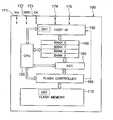
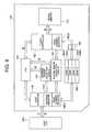
- FIG. 1is a block diagram showing an embodiment of a memory card containing a non-volatile memory to which the present invention is applied.
- FIG. 2is a timing diagram showing a first embodiment of write processing that is performed when the present invention is applied to the memory card in FIG. 1.
- FIG. 3is a timing diagram showing a second embodiment of write processing on the memory card to which the present invention is applied.
- FIG. 4is a block diagram showing an example of the configuration of hardware that implements the second embodiment of write processing on the memory card to which the present invention is applied.
- FIG. 5is a flowchart showing a control procedure used in the second embodiment of write processing on the memory card to which the present invention is applied.
- FIG. 6is a timing diagram showing a third embodiment of write processing on the memory card to which the present invention is applied.
- FIG. 7is a timing diagram showing a fourth embodiment of write processing on the memory card to which the present invention is applied.
- FIG. 8is a block diagram showing an example of the configuration of hardware that implements the fifth embodiment of write processing on the memory card to which the present invention is applied.
- FIG. 9is a flowchart showing a control procedure used in the fifth embodiment of write processing on the memory card to which the present invention is applied.
- FIG. 10is a timing diagram showing the timing of write processing on a conventional memory card.
- FIG. 11is a block diagram showing an operation performed when a write error occurs on a memory card using a flash memory that has a data latch holding write data.
- FIG. 1shows an embodiment of a memory card containing a non-volatile memory according to the present invention.
- a memory card 100 in this embodimentcomprises a flash memory (FLASH) 110 from which a predetermined amount of data may be electrically erased at a time, a microprocessor (CPU) 120 that controls the whole internal operations of the card, such as data transfer, based on externally supplied commands, an interface circuit 130 that transfers signals to and from external devices, a buffer memory 140 , including of a RAM and so on, that stores write data sent from external devices and read data sent from the flash memory 110 , an error-correction-code generation & error correction circuit 150 that generates an error correction code for write data and that checks and corrects read data based on the error correction code, and a flash controller 160 that controls writing data to and reading data from the flash memory 110 in response to an instruction from the CPU 120 .
- FLASHflash memory
- CPUmicroprocessor
- the components of the memory cardsuch as the memory 110 , CPU 120 , and flash controller 160 , each including of a semiconductor integrated circuit.
- Those semiconductor integrated circuitswhich are mounted on a printed circuit board, are molded with resin to form the memory card 100 .
- the external terminals 171 - 175are electrically connected to the circuit of an external electronic device when the memory card is inserted into the card slot of the external electronic device.
- the external terminals 171 and 172are the power terminal and the ground terminal that are connected to the power potential Vcc and the ground potential GND, respectively.
- the external terminal 173receives a clock signal CK used to time the operation.
- the external terminal 174is a terminal through which a command or an address sent from an external host CPU to the card is input and through which the contents of the status register are output from the card to the host CPU.
- the external terminal 175is a terminal through which write data sent from the external host CPU to the card is input and through which read data read from the card is output to the host CPU.
- the buffer memory 140comprises a plurality of banks.
- the bank specification signal and the read/write indication signalare supplied from the microprocessor 120 to the buffer memory 140 .
- the bank status indication signalis supplied from the buffer memory 140 to the microprocessor 120 .
- Write data transferred from the external host CPUis stored sequentially in the specified bank in the buffer memory 140 and, via the error-correction-code generation & error correction circuit 150 , supplied to the flash memory 110 .
- the microprocessor 120converts a logical address entered from the external terminal 174 to a physical address and supplies the converted address to the flash memory 110 via the flash controller 160 .
- the synchronization clock SCis supplied from the microprocessor 120 to the error-correction-code generation & error correction circuit 150 , and the signal indicating whether or not an error has been successfully corrected is supplied from the error-correction-code generation & error correction circuit 150 to the microprocessor 120 .
- the interface circuit 130includes a status register SR 1 that contains an indicator indicating the status of the card, for example, whether or not write data has been transferred from the buffer memory 140 to the flash memory 110 .
- the status of the cardis set in the status register SR 1 by a signal from the microprocessor 120 .
- the status bits of the status register SR 1include, for example, an error bit indicating that a write error has occurred, a ready/busy bit indicating that the card may be accessed, and an overflow bit indicating that the buffer memory 140 is full.
- the contents of the status register SR 1may be read by a register read command, sent from the external host CPU, via the external terminal 174 via which the command is also input.
- the memory cardmay also be configured such that the status of the flash memory 110 is written directly into the status register SR 1 by a signal sent from the flash controller 160 .
- the flash memory 110comprises a memory array that is a matrix of non-volatile memory cells including of insulated-gate field effect transistors each with a floating gate, a word decoder that decodes an externally supplied address signal and activates the corresponding word line in the memory array to set it to the selection level, a data latch connected to the bit lines within the memory array to hold read/write data, and a boosting circuit that generates a high voltage required for writing and erasure.
- the data latchshould be large enough to store data of one sector, that is, data of all memory cells connected to one word line.
- the flash memory 110contains a status register SR 2 that indicates whether data has been written normally or an error has occurred.
- a flash memorywith a two-layer gate structure, stores data by taking advantage of a difference between the threshold voltage levels of the charge stored in the floating gate layer.
- injecting electrons into the floating gate layer to increase the threshold voltageis called a write, and the reverse operation is called an erasure.
- the flash memory used in the memory card in this embodimentis built such that it performs operation based on commands and control signals.
- Commands that may be issued to the flash memoryinclude a read command, a write command, and an erase command.
- Control signals that are sent to the flash memory 110include a chip select signal CE, a write control signal WE indicating whether the operation is a read operation or a write operation, an output control signal OE that indicates a time at which data is output, a system clock SC, and a command enable signal CDE that indicates which input has been received, command or address.
- Those commands and control signalsare given by the flash controller 160 .
- the flash controller 160has a control register.
- the microprocessor 120sets up this control register to cause the flash controller 160 to control the operations, such as a write, read, and erase, to be performed for the flash memory 110 .
- Signals supplied from the microprocessor 120 to the flash controller 160include a control signal indicating which operation, read or write, is to be performed, an address signal specifying the control register and so on, and a data signal indicating data to be stored in the control register.
- the configuration of a memory card on which a flash memory is mountedis not limited to that shown in FIG. 1.
- the memory cardmay use a flash memory that contains the error-correction-code generation & error correction circuit or may use a chip that combines the error-correction-code generation & error correction circuit with the controller.
- the flash memory 110may be either a binary flash memory in which one-bit data is stored in one memory cell or a multi-valued flash memory in which multiple-bit data is stored in one memory cell by controlling the threshold voltage.
- flash memoriesmay be mounted.
- ECC circuitsmay be provided, one for each chip, or one ECC circuit may be shared among multiple flash memories.
- the memory card in this embodimenthas two controllers, that is, microprocessor 120 and flash controller 160 , the memory card may have only one of them.
- the buffer memory 140is assumed to include four banks, BNK 0 -BNK 3 , each with the capacity of 512 bytes.
- a data transfer command and a write addressare first sent from an external host CPU to the external terminal 174 of the memory card (period T1). Then, write data is transferred from the host CPU to the external terminal 175 of the memory card. The transferred data is stored sequentially into banks BNK 0 -BNK 3 of the buffer memory 140 via the interface 130 (period T2). The transmission of the command and the address and the transfer of write data described above are performed serially.
- write datais transferred from each bank to the flash memory 110 when each of banks BNK 0 , BNK 1 , BNK 2 , and BNK 3 is filled with transfer data DATA 0 , DATA 1 , DATA 2 , and DATA 3 each in 512 bytes (period T3).
- bank 0is filled with transfer data DATA 0
- the transfer of the next data, DATA 1from the host CPU to bank BNK 1 starts and, concurrently with this transfer, data is transferred from bank BNK 0 to the flash memory 110 .
- Datais transferred from each bank to the flash memory 110 in parallel, for example, eight bits at a time. Therefore, for 512-byte data stored in one bank, the transfer of the data from the buffer memory 140 to the flash memory 110 is faster than the transfer of the data from the host CPU to the buffer memory 140 .
- write datagoes through the error-correction-code generation & error correction circuit 150 to have an error correction code attached, one for each 512 bytes, before being supplied to the flash memory 110 .
- datahas been transferred from banks BNK 0 -BNK 3 to the flash memory 110 , one sector of data is written into the flash memory 110 (period T4).
- the bit indicating the end of data transferis set in the status register SR 1 in the interface circuit 130 .
- the external host CPUsends a read command of the status register SR 1 to find that data has been transferred from the buffer memory.
- the contents of the status register SR 1are sent to the host CPU via the external terminal 174 , via which the command was input, in the time-division manner.
- the transfer of data, which is to be written into the next sector, from the external host CPU to the memory cardmay be started without having to wait until data is written into the flash memory 110 . This reduces the overhead time involved in write data transfer and reduces the total write time.
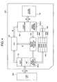
- FIG. 4shows hardware required for preventing a data transfer outstrip condition.
- the interface circuit 130contains register REG 1 in which the number of the bank of the buffer memory 140 whose data is being transferred by a host CPU 200 is stored.
- the flash controller 160contains register REG 2 in which the number of the bank whose data is being transferred from the buffer memory 140 to the flash memory 110 is stored.
- a buffer error detection circuit 180including a comparator comparing the bank numbers of the two registers, REG 1 and REG 2 , is provided. Registers REG 1 and REG 2 are managed by the interface circuit 130 and the flash controller 160 , respectively.
- the buffer error detection circuit 180outputs a detection signal to the microprocessor 120 when the bank numbers stored in the two registers match.
- the microprocessor 120Upon detecting that the transfer of data from the host CPU 200 is made to the bank in use, the microprocessor 120 , for example, sets the data transfer error bit in status register SR 1 in the interface circuit 130 to inform the host CPU 200 of a data transfer error.
- the data transfer error bitmay also indicate an error other than the data transfer outstrip error (buffer error), or another bit indicating only the buffer error may be provided to distinguish between the buffer error and other data transfer errors.
- the host CPU 200may read the contents of status register SR 1 by issuing the read command, as described above, to check if a data transfer error has occurred. Therefore, if a data transfer error occurred, it is necessary to send the write command and transfer write data to start from the beginning.
- the time required to write data into the flash memorydepends on a sector into which data is to be written or on data that is written. Sometimes, the write time is extremely long. Therefore, even if the host CPU tries to transfer data according to the average flash-memory write time, a buffer error may occur as described above. In this embodiment, information about a data transfer strip may be sent to the host CPU. As a result, this method prevents the host CPU from transferring the next data into a bank before the data in that bank is transferred to the flash memory.
- the buffer error detection circuit 180is provided to allow the hardware to detect a data transfer outstrip condition. This may also be achieved by the software in the microprocessor 120 .
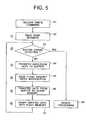
- FIG. 5shows an example of the control procedure.
- the microprocessor 120In response to a write command from the host CPU, the microprocessor 120 reads bank numbers from registers REG 1 and REG 2 and compares them to check if a buffer error has occurred (steps S 1 -S 3 ). If no error buffer has occurred, write data transferred from the host CPU is stored in the bank of the buffer memory corresponding to the bank number indicated by register REG 1 (step S 4 ).
- the microprocessor 120issues a write instruction, which writes data into the flash memory 110 , to the flash controller 160 and transfers data from the buffer memory 140 to the flash memory 110 (steps S 5 and S 6 ). After that, the microprocessor 120 issues a flash-memory write start instruction to the flash controller 160 and then passes control back to step S 3 (step S 7 ). On the other hand, if it is found in step S 3 that a buffer error has occurred, the microprocessor 120 passes control to step S 8 and performs error processing; for example, it sets the data transfer error bit in the status register SR 1 in the interface circuit 130 .
- This embodimentmay be configured, for example, to provide a register, in which information indicating the bank number or transfer data where a buffer error occurred is stored, in the interface circuit 130 to inform the host CPU of the condition.
- a buffer erroroccurs during the data transfer from the host CPU to the memory card, this configuration allows the data transfer to be restarted from the data where an error occurred.
- register REG 1containing the number of the bank of the buffer memory 140 being used by the host CPU 200 for data transfer is provided in the interface circuit 130
- register REG 2containing the number of the bank to which data is being transferred from the buffer memory 140 to the flash memory 110 is provided in the flash controller 160 .
- the location of those registersis not limited to the configuration described above. Those registers may be provided either as independent circuits or in a part of the microprocessor 120 or the buffer memory 140 .
- registers REG 1 and REG 2may be provided for each bank, one indicating that data is being transferred between the host CPU and the buffer memory and the other indicating that data is being transferred between the buffer memory and the flash memory, to detect a buffer error based on the state of those flags.
- a register containing the number of a bank that causes a buffer errormay be provided in the interface circuit 130 so that the external host CPU may read it.
- the transfer method in the third embodimentis similar to that in the second embodiment. That is, after data DATA 0 -DATA 3 has been transferred to all banks BNK 0 -BNK 43 of the buffer memory 140 , data, DATA 4 -DATA 7 , to be written into the next sector is immediately transferred without checking if data has been transferred from the buffer memory 140 to the flash memory 110 .
- the difference from the transfer method in the second embodimentis that a buffer error occurs when an attempt is made to transfer the next data if all banks contain data not yet transferred as shown in the buffer memory status diagram at the bottom of FIG. 6 (timing t2).
- a shaded bankindicates that data from the host CPU is stored but the data is not yet transferred to the flash memory.
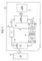
- FIG. 7shows hardware required when the transfer method in the third embodiment is applied.
- flags FLG 0 -FLG 3each corresponding to banks BNK 0 -BNK 3 in the buffer memory 140 .
- Each flagis set to “1” when the host CPU 200 stores data in the corresponding bank, and is cleared to “0” when the stored data is transferred to the flash memory 110 . Therefore, regardless of whether data is actually stored in the bank, the bank is free if the flag is “0” and is able to receive the next write data.
- the method described belowis used although the present invention is not limited to this method. That is, the flag of a bank into which the interface circuit 130 is going to store data during the transfer of data from the host CPU 200 to the buffer memory 140 is set to “1” and the flag is cleared to “0” when the microprocessor 120 has transferred one bank of data from the buffer memory 140 to the flash memory 110 .
- step S 2flags FLG 0 -FLG 3 in the buffer memory 140 are read instead of reading a bank number from the register and that, in step S 3 , it is determined that a buffer error has occurred, not when the bank numbers match, but when flags FLG 0 -FLG 3 all contain “1”.
- a registerwhich contains the number of a bank to which data has been transferred from the host CPU, may be provided.
- the bank numberis deleted from the register. Based on the contents of this register, a check is made to see if a buffer error has occurred.
- the method in this embodimentprevents a flash memory write failure or a flash memory overflow from being generated because of an address error when data is written into the flash memory 110 using a write command and write data sent from the host CPU. That is, as described in the embodiments described above, when the write address attached to the write command sent from the host CPU is out of the allowable address range of the flash memory 110 or, for example, when more than one sector of write data is sent from the host CPU following the write address specifying the last sector in the flash memory, a flash memory overflow occurs and data cannot be written.
- the object of this embodimentis to prevent this error.
- the memory card in this embodimenthas an address setting register ADR and an address error detection circuit 190 as shown in FIG. 8.
- the address setting register ADRis provided in the interface circuit 130 to contain the address range of the flash memory.
- the address error detection circuit 190compares a physical address generated by the microprocessor 120 by converting a logical address supplied from the host CPU or an address updated by the microprocessor 120 according to the transfer data amount with the address stored in the address setting register ADR.
- the address setting register ADR described abovemay be provided, not in the interface circuit 130 , but as an independent circuit or in the flash controller 160 or microprocessor 120 .
- the memory card in this embodimentis combined with the memory card in the embodiment in FIG. 4, that is, the memory card has REG 1 and REG 2 containing the numbers of the banks from or to which data is being transferred and the buffer error detection circuit 180 are provided, this embodiment may be independent of the embodiment in FIG. 4. That is, registers REG 1 and REG 2 and the buffer error detection circuit 180 shown in FIG. 8 may be omitted.
- step 9in which a check is made for an address error, is inserted between step S 4 and step S 5 in FIG. 5 and that, if an address error is generated, control is passed to error processing S 8 in which a predetermined error bit in status register SR 1 in the interface circuit 130 is set.
- the address error check in step S 9 in FIG. 9may be made based on the signal from the address error detection circuit 190 . It is also possible for the microprocessor 120 to make the address error check on a software basis, based on the address that is set in the address setting register ADR, with no address error detection circuit 190 provided.
- the write data which is stored in the data latch DL in the flash memory 110 and for which the write error occurredis read into an area other than bank 0 -bank 3 of the buffer memory 140 , substitute processing is performed by specifying an alternate address in the flash memory 110 other than the address where the error occurred, and then the write error which has been read into the buffer memory 140 and for which the write error occurred is stored again at the alternate address. After data is stored in the alternate address, the next write data stored in bank 0 -bank 3 of the buffer memory 140 is stored. This method eliminates the need for transferring again the write data that was transferred from the host CPU 200 .
- the buffer memory 140 in the above embodimentsincludes four banks, the number of banks is not limited to four but any number of buffers may be used.
- the buffer memory 140may include one semiconductor memory, it may also include a plurality of semiconductor memories. In this case, one semiconductor memory may be made correspond to one bank.
- the buffer memory 140 larger than one sector of flash memory 110may be used, to allow a non-bank area to be used as the work area of the microprocessor 120 .
- the invention made by the inventorsis described primarily for flash memory and a memory card containing a flash memory that is in the background field of the invention.
- the present inventionis not limited to the memory card described above.
- the present inventionmay be applied also to EEPROM chips, other non-volatile memories, memory cards containing such memories, and a memory module including a board on which a plurality of non-volatile memory chips are mounted.
- the buffer memoryincludes a plurality of banks. Data is transferred sequentially from a host CPU to the banks of the buffer memory, data is transferred to the non-volatile memory from a bank that becomes full, the write operation is started when one unit of data to be written into the non-volatile memory at a time has been transferred and, without waiting for the data to be written, the next write data is transferred from the host CPU to a bank from which write data has been transferred. This method reduces the write data transfer overhead and reduces the time required for writing data.
Landscapes
- Read Only Memory (AREA)
- Techniques For Improving Reliability Of Storages (AREA)
- Memory System (AREA)
Abstract
Description
- The present invention relates to a technology that may be applied to a non-volatile storage device, for example, to a technology that may be applied to a non-volatile semiconductor memory such as a flash memory or a card storage device, such as a multimedia card or a smart media memory card, that contains such a non-volatile semiconductor memory.[0001]
- Recently, a card storage device, called a memory card containing a non-volatile memory, such as a flash memory, that retains its storage data even after the power has been switched off, is widely used as a data storage medium for portable electronic apparatus such as a digital camera.[0002]
- Unlike a volatile memory such as a RAM, a non-volatile memory requires a longer write time. To solve this problem, some memory cards that contain a non-volatile memory further contain a buffer memory including of a RAM with a memory amount smaller than that of the non-volatile memory. When storing data, write data transferred from an external host CPU is once transferred to this buffer memory and then sequentially transferred from this buffer memory to the non-volatile memory (for example, JP-A-2-62687 laid-open on Mar. 2, 1990).[0003]
- However, a conventional memory card that contains a buffer memory transfers data as follows. That is, as shown in FIG. 10, a write command is sent during period T1 and a predetermined amount of write data is transferred from the host CPU to the buffer memory during period T2. Then, during period T3, one unit of data that is written at a time is transferred from the buffer memory to the non-volatile memory. On the other hand, after sending data DATA[0004]3, the host CPU stops data transfer to the buffer memory and waits until data is written in the non-volatile memory (period T4). Then, after confirming that data has been written on the memory card, the next write data is transferred from the host CPU to the buffer memory (period T5′).
- The advantage of this method is that, even if the write operation fails for some reason, the write data need not be transferred again from the host CPU to the memory card because the write data is retained in the buffer memory for period T4 during which the write data is written into the non-volatile memory. However, the problem with this method is that the overhead is large and that total write time is long because, for period T4 during which data is written into the non-volatile memory, data transfer to the buffer memory is suspended and the host CPU is put in the wait state and because the write operation of the non-volatile memory is also put in the wait state for the period during which the next data is transferred from the host CPU to the buffer memory.[0005]
- It is an object of the present invention to provide a technology that reduces the write-data transfer overhead of a card storage device containing a non-volatile memory and a buffer memory to reduce the data write time.[0006]
- The above-described objects and other objects, as well as the new features, of the present invention will be made more apparent by the detailed description and the accompanying drawings of this specification.[0007]
- According to one aspect of the present invention, in a card storage device containing a non-volatile memory and a buffer memory, the buffer memory includes of a plurality of banks. Data is transferred sequentially from a host CPU to the banks of the buffer memory and data is transferred to the non-volatile memory from a bank that becomes full. The write operation is started when one unit of data to be written into the non-volatile memory at a time has been transferred and, without waiting for the data to be written, the next write data is transferred from the host CPU to a bank from which write data has been transferred.[0008]
- According to the above aspect, data is transferred from the host CPU to the buffer memory concurrently with the data transfer from the buffer memory to the non-volatile memory. This method reduces the write data transfer overhead and greatly reduces the time required for writing data.[0009]
- According to another aspect of the present invention, the card storage device further comprises a status register or a status flag indicating a completion/incompletion of the data transfer from the buffer memory to the non-volatile memory, wherein the status of the status register or the status flag are controlled by the controller. This configuration allows the host CPU to reference the status register or the status flag and to determine easily whether the next data may be transferred from the host CPU to the buffer memory.[0010]
- According to another aspect of the present invention, the card storage device further comprises a first register containing information on a bank into which data is being entered from the external unit; and a second register containing information on a bank from which data is being transferred from the buffer memory to the non-volatile memory, wherein the controller judges the completion/incompletion of the data transfer to or from each bank, based on the bank information in the first register and the second register, to control the status register or the status flag. Alternatively, the card storage device further comprises a flag, for each bank, indicating whether or not the corresponding bank has data to be transferred to the non-volatile memory, wherein the controller judges the completion/incompletion of the data transfer to or from each bank, based on the flag status, to control the status register or the status flag. This configuration makes it easy to concurrently control the transfer of data from the buffer memory to the non-volatile memory and the transfer of data from the host CPU to the buffer memory.[0011]
- Other objects, features and advantages of the invention will become apparent from the following description of the embodiments of the invention taken in conjunction with the accompanying drawings.[0012]
- FIG. 1 is a block diagram showing an embodiment of a memory card containing a non-volatile memory to which the present invention is applied.[0013]
- FIG. 2 is a timing diagram showing a first embodiment of write processing that is performed when the present invention is applied to the memory card in FIG. 1.[0014]
- FIG. 3 is a timing diagram showing a second embodiment of write processing on the memory card to which the present invention is applied.[0015]
- FIG. 4 is a block diagram showing an example of the configuration of hardware that implements the second embodiment of write processing on the memory card to which the present invention is applied.[0016]
- FIG. 5 is a flowchart showing a control procedure used in the second embodiment of write processing on the memory card to which the present invention is applied.[0017]
- FIG. 6 is a timing diagram showing a third embodiment of write processing on the memory card to which the present invention is applied.[0018]
- FIG. 7 is a timing diagram showing a fourth embodiment of write processing on the memory card to which the present invention is applied.[0019]
- FIG. 8 is a block diagram showing an example of the configuration of hardware that implements the fifth embodiment of write processing on the memory card to which the present invention is applied.[0020]
- FIG. 9 is a flowchart showing a control procedure used in the fifth embodiment of write processing on the memory card to which the present invention is applied.[0021]
- FIG. 10 is a timing diagram showing the timing of write processing on a conventional memory card.[0022]
- FIG. 11 is a block diagram showing an operation performed when a write error occurs on a memory card using a flash memory that has a data latch holding write data.[0023]
- Some preferred embodiments of the present invention will be described below with reference to the drawings.[0024]
- FIG. 1 shows an embodiment of a memory card containing a non-volatile memory according to the present invention.[0025]
- Although not limited to this configuration, a[0026]
memory card 100 in this embodiment comprises a flash memory (FLASH)110 from which a predetermined amount of data may be electrically erased at a time, a microprocessor (CPU)120 that controls the whole internal operations of the card, such as data transfer, based on externally supplied commands, aninterface circuit 130 that transfers signals to and from external devices, abuffer memory 140, including of a RAM and so on, that stores write data sent from external devices and read data sent from theflash memory 110, an error-correction-code generation &error correction circuit 150 that generates an error correction code for write data and that checks and corrects read data based on the error correction code, and aflash controller 160 that controls writing data to and reading data from theflash memory 110 in response to an instruction from theCPU 120. - The components of the memory card, such as the[0027]
memory 110,CPU 120, andflash controller 160, each including of a semiconductor integrated circuit. Those semiconductor integrated circuits, which are mounted on a printed circuit board, are molded with resin to form thememory card 100. - Also provided on the[0028]
memory card 100 in this embodiment are external terminals171-175 that are electrically connected to the circuit of an external electronic device when the memory card is inserted into the card slot of the external electronic device. Theexternal terminals external terminal 173 receives a clock signal CK used to time the operation. Theexternal terminal 174 is a terminal through which a command or an address sent from an external host CPU to the card is input and through which the contents of the status register are output from the card to the host CPU. Theexternal terminal 175 is a terminal through which write data sent from the external host CPU to the card is input and through which read data read from the card is output to the host CPU. - Signals are input and output from the[0029]
external terminals interface circuit 130. Thebuffer memory 140 comprises a plurality of banks. The bank specification signal and the read/write indication signal are supplied from themicroprocessor 120 to thebuffer memory 140. The bank status indication signal is supplied from thebuffer memory 140 to themicroprocessor 120. Write data transferred from the external host CPU is stored sequentially in the specified bank in thebuffer memory 140 and, via the error-correction-code generation &error correction circuit 150, supplied to theflash memory 110. Themicroprocessor 120 converts a logical address entered from theexternal terminal 174 to a physical address and supplies the converted address to theflash memory 110 via theflash controller 160. - The synchronization clock SC is supplied from the[0030]
microprocessor 120 to the error-correction-code generation &error correction circuit 150, and the signal indicating whether or not an error has been successfully corrected is supplied from the error-correction-code generation &error correction circuit 150 to themicroprocessor 120. Theinterface circuit 130 includes a status register SR1 that contains an indicator indicating the status of the card, for example, whether or not write data has been transferred from thebuffer memory 140 to theflash memory 110. - The status of the card is set in the status register SR[0031]1 by a signal from the
microprocessor 120. The status bits of the status register SR1 include, for example, an error bit indicating that a write error has occurred, a ready/busy bit indicating that the card may be accessed, and an overflow bit indicating that thebuffer memory 140 is full. In this embodiment, the contents of the status register SR1 may be read by a register read command, sent from the external host CPU, via theexternal terminal 174 via which the command is also input. The memory card may also be configured such that the status of theflash memory 110 is written directly into the status register SR1 by a signal sent from theflash controller 160. - The[0032]
flash memory 110 comprises a memory array that is a matrix of non-volatile memory cells including of insulated-gate field effect transistors each with a floating gate, a word decoder that decodes an externally supplied address signal and activates the corresponding word line in the memory array to set it to the selection level, a data latch connected to the bit lines within the memory array to hold read/write data, and a boosting circuit that generates a high voltage required for writing and erasure. - In the flash memory in this embodiment, the data latch should be large enough to store data of one sector, that is, data of all memory cells connected to one word line. In addition, the[0033]
flash memory 110 contains a status register SR2 that indicates whether data has been written normally or an error has occurred. - A flash memory, with a two-layer gate structure, stores data by taking advantage of a difference between the threshold voltage levels of the charge stored in the floating gate layer. In this embodiment, injecting electrons into the floating gate layer to increase the threshold voltage is called a write, and the reverse operation is called an erasure.[0034]
- The flash memory used in the memory card in this embodiment is built such that it performs operation based on commands and control signals. Commands that may be issued to the flash memory include a read command, a write command, and an erase command. Control signals that are sent to the[0035]
flash memory 110 include a chip select signal CE, a write control signal WE indicating whether the operation is a read operation or a write operation, an output control signal OE that indicates a time at which data is output, a system clock SC, and a command enable signal CDE that indicates which input has been received, command or address. Those commands and control signals are given by theflash controller 160. - The[0036]
flash controller 160 has a control register. Themicroprocessor 120 sets up this control register to cause theflash controller 160 to control the operations, such as a write, read, and erase, to be performed for theflash memory 110. Signals supplied from themicroprocessor 120 to theflash controller 160 include a control signal indicating which operation, read or write, is to be performed, an address signal specifying the control register and so on, and a data signal indicating data to be stored in the control register. - The configuration of a memory card on which a flash memory is mounted is not limited to that shown in FIG. 1. The memory card may use a flash memory that contains the error-correction-code generation & error correction circuit or may use a chip that combines the error-correction-code generation & error correction circuit with the controller. In addition, the[0037]
flash memory 110 may be either a binary flash memory in which one-bit data is stored in one memory cell or a multi-valued flash memory in which multiple-bit data is stored in one memory cell by controlling the threshold voltage. - Furthermore, rather than mounting only one flash memory, multiple flash memories may be mounted. In that case, ECC circuits may be provided, one for each chip, or one ECC circuit may be shared among multiple flash memories. Although the memory card in this embodiment has two controllers, that is,[0038]
microprocessor 120 andflash controller 160, the memory card may have only one of them. - A first embodiment of the write data transfer method that is used when the present invention is applied to the memory card with the configuration described above will be described with reference to the timing diagram in FIG. 2. In the description below, the[0039]
buffer memory 140 is assumed to include four banks, BNK0-BNK3, each with the capacity of 512 bytes. - In the first embodiment, when data is written in the memory card, a data transfer command and a write address are first sent from an external host CPU to the[0040]
external terminal 174 of the memory card (period T1). Then, write data is transferred from the host CPU to theexternal terminal 175 of the memory card. The transferred data is stored sequentially into banks BNK0-BNK3 of thebuffer memory 140 via the interface130 (period T2). The transmission of the command and the address and the transfer of write data described above are performed serially. - Concurrently with the transfer of write data to the[0041]
buffer memory 140 described above, write data is transferred from each bank to theflash memory 110 when each of banks BNK0, BNK1, BNK2, and BNK3 is filled with transfer data DATA0, DATA1, DATA2, and DATA3 each in 512 bytes (period T3). For example, whenbank 0 is filled with transfer data DATA0, the transfer of the next data, DATA1, from the host CPU to bank BNK1 starts and, concurrently with this transfer, data is transferred from bank BNK0 to theflash memory 110. - Data is transferred from each bank to the[0042]
flash memory 110 in parallel, for example, eight bits at a time. Therefore, for 512-byte data stored in one bank, the transfer of the data from thebuffer memory 140 to theflash memory 110 is faster than the transfer of the data from the host CPU to thebuffer memory 140. In addition, when transferred from thebuffer memory 140 to theflash memory 110, write data goes through the error-correction-code generation &error correction circuit 150 to have an error correction code attached, one for each 512 bytes, before being supplied to theflash memory 110. When data has been transferred from banks BNK0-BNK3 to theflash memory 110, one sector of data is written into the flash memory110 (period T4). - On the other hand, when all write data has been transferred from the[0043]
buffer memory 140 to theflash memory 110 in this embodiment, the data in thebuffer memory 140 is treated as unnecessary data. Then, data DATA4-DATA7 to be written into the next sector is transferred to the buffer memory140 (period T5). - When all write data has been transferred from the[0044]
buffer memory 140 to theflash memory 110, the bit indicating the end of data transfer is set in the status register SR1 in theinterface circuit 130. The external host CPU sends a read command of the status register SR1 to find that data has been transferred from the buffer memory. The contents of the status register SR1 are sent to the host CPU via theexternal terminal 174, via which the command was input, in the time-division manner. - According to the data transfer method in this embodiment, the transfer of data, which is to be written into the next sector, from the external host CPU to the memory card may be started without having to wait until data is written into the[0045]
flash memory 110. This reduces the overhead time involved in write data transfer and reduces the total write time. - A second embodiment of the write data transfer method for use on the memory card according to the present invention will be described with reference to the timing diagram in FIG. 3.[0046]
- In the transfer method in the second embodiment, after one sector of data has been transferred to all banks of the[0047]
buffer memory 140, data to be written into the next sector is immediately transferred without reading status register SR1 to check, as in the first embodiment, if the transfer of data to the flash memory is ended. However, in this case, if the time required to transfer data from the host CPU to thebuffer memory 140 is shorter than the time required to write data into theflash memory 110, the time to start the transfer of write data from the host CPU to thebuffer memory 140 sometimes arrives before data already stored in thebuffer memory 140 is transferred to theflash memory 110 as indicated by code t1 in FIG. 3. - Therefore, when using the transfer method in this embodiment, it is necessary to prevent a data transfer outstrip condition such as the one described above. One example of a data transfer outstrip prevention method will be described with reference to FIGS. 4 and 5.[0048]
- FIG. 4 shows hardware required for preventing a data transfer outstrip condition. The[0049]
interface circuit 130 contains register REG1 in which the number of the bank of thebuffer memory 140 whose data is being transferred by ahost CPU 200 is stored. Theflash controller 160 contains register REG2 in which the number of the bank whose data is being transferred from thebuffer memory 140 to theflash memory 110 is stored. In addition, a buffererror detection circuit 180 including a comparator comparing the bank numbers of the two registers, REG1 and REG2, is provided. Registers REG1 and REG2 are managed by theinterface circuit 130 and theflash controller 160, respectively. - In this embodiment, the buffer[0050]
error detection circuit 180 outputs a detection signal to themicroprocessor 120 when the bank numbers stored in the two registers match. Upon detecting that the transfer of data from thehost CPU 200 is made to the bank in use, themicroprocessor 120, for example, sets the data transfer error bit in status register SR1 in theinterface circuit 130 to inform thehost CPU 200 of a data transfer error. The data transfer error bit may also indicate an error other than the data transfer outstrip error (buffer error), or another bit indicating only the buffer error may be provided to distinguish between the buffer error and other data transfer errors. - The[0051]
host CPU 200 may read the contents of status register SR1 by issuing the read command, as described above, to check if a data transfer error has occurred. Therefore, if a data transfer error occurred, it is necessary to send the write command and transfer write data to start from the beginning. - In general, the time required to write data into the flash memory depends on a sector into which data is to be written or on data that is written. Sometimes, the write time is extremely long. Therefore, even if the host CPU tries to transfer data according to the average flash-memory write time, a buffer error may occur as described above. In this embodiment, information about a data transfer strip may be sent to the host CPU. As a result, this method prevents the host CPU from transferring the next data into a bank before the data in that bank is transferred to the flash memory.[0052]
- On the memory card in the embodiment in FIG. 4, the buffer[0053]
error detection circuit 180 is provided to allow the hardware to detect a data transfer outstrip condition. This may also be achieved by the software in themicroprocessor 120. FIG. 5 shows an example of the control procedure. - In response to a write command from the host CPU, the[0054]
microprocessor 120 reads bank numbers from registers REG1 and REG2 and compares them to check if a buffer error has occurred (steps S1-S3). If no error buffer has occurred, write data transferred from the host CPU is stored in the bank of the buffer memory corresponding to the bank number indicated by register REG1 (step S4). - When the bank becomes full, the[0055]
microprocessor 120 issues a write instruction, which writes data into theflash memory 110, to theflash controller 160 and transfers data from thebuffer memory 140 to the flash memory110 (steps S5 and S6). After that, themicroprocessor 120 issues a flash-memory write start instruction to theflash controller 160 and then passes control back to step S3 (step S7). On the other hand, if it is found in step S3 that a buffer error has occurred, themicroprocessor 120 passes control to step S8 and performs error processing; for example, it sets the data transfer error bit in the status register SR1 in theinterface circuit 130. - This embodiment may be configured, for example, to provide a register, in which information indicating the bank number or transfer data where a buffer error occurred is stored, in the[0056]
interface circuit 130 to inform the host CPU of the condition. When a buffer error occurs during the data transfer from the host CPU to the memory card, this configuration allows the data transfer to be restarted from the data where an error occurred. - In FIG. 4, register REG[0057]1 containing the number of the bank of the
buffer memory 140 being used by thehost CPU 200 for data transfer is provided in theinterface circuit 130, and register REG2 containing the number of the bank to which data is being transferred from thebuffer memory 140 to theflash memory 110 is provided in theflash controller 160. The location of those registers is not limited to the configuration described above. Those registers may be provided either as independent circuits or in a part of themicroprocessor 120 or thebuffer memory 140. - Alternatively, instead of providing registers REG[0058]1 and REG2, two flags may be provided for each bank, one indicating that data is being transferred between the host CPU and the buffer memory and the other indicating that data is being transferred between the buffer memory and the flash memory, to detect a buffer error based on the state of those flags. In addition, a register containing the number of a bank that causes a buffer error may be provided in the
interface circuit 130 so that the external host CPU may read it. - A third embodiment of the write data transfer method for use on the memory card according to the present invention will be described with reference to the timing diagram in FIG. 6.[0059]
- The transfer method in the third embodiment is similar to that in the second embodiment. That is, after data DATA[0060]0-DATA3 has been transferred to all banks BNK0-BNK43 of the
buffer memory 140, data, DATA4-DATA7, to be written into the next sector is immediately transferred without checking if data has been transferred from thebuffer memory 140 to theflash memory 110. The difference from the transfer method in the second embodiment is that a buffer error occurs when an attempt is made to transfer the next data if all banks contain data not yet transferred as shown in the buffer memory status diagram at the bottom of FIG. 6 (timing t2). In the buffer memory status diagram at the bottom of FIG. 6, a shaded bank indicates that data from the host CPU is stored but the data is not yet transferred to the flash memory. - FIG. 7 shows hardware required when the transfer method in the third embodiment is applied. In this embodiment, flags FLG[0061]0-FLG3, each corresponding to banks BNK0-BNK3 in the
buffer memory 140, are provided. Each flag is set to “1” when thehost CPU 200 stores data in the corresponding bank, and is cleared to “0” when the stored data is transferred to theflash memory 110. Therefore, regardless of whether data is actually stored in the bank, the bank is free if the flag is “0” and is able to receive the next write data. - In this embodiment, the method described below is used although the present invention is not limited to this method. That is, the flag of a bank into which the[0062]
interface circuit 130 is going to store data during the transfer of data from thehost CPU 200 to thebuffer memory 140 is set to “1” and the flag is cleared to “0” when themicroprocessor 120 has transferred one bank of data from thebuffer memory 140 to theflash memory 110. - The control procedure of the[0063]
microprocessor 120 used for data transfer in this embodiment is almost the same as the flowchart shown in FIG. 5. The only difference is that, in step S2, flags FLG0-FLG3 in thebuffer memory 140 are read instead of reading a bank number from the register and that, in step S3, it is determined that a buffer error has occurred, not when the bank numbers match, but when flags FLG0-FLG3 all contain “1”. - Instead of providing the flags, it is also possible to provide a register, which contains the number of a bank to which data has been transferred from the host CPU, may be provided. When data has been transferred from the bank to the flash memory, the bank number is deleted from the register. Based on the contents of this register, a check is made to see if a buffer error has occurred.[0064]
- Next, a fourth embodiment of the write data transfer method for use on the memory card according to the present invention will be described with reference to the block diagram in FIG. 8 and the flowchart in FIG. 9.[0065]
- The method in this embodiment prevents a flash memory write failure or a flash memory overflow from being generated because of an address error when data is written into the[0066]
flash memory 110 using a write command and write data sent from the host CPU. That is, as described in the embodiments described above, when the write address attached to the write command sent from the host CPU is out of the allowable address range of theflash memory 110 or, for example, when more than one sector of write data is sent from the host CPU following the write address specifying the last sector in the flash memory, a flash memory overflow occurs and data cannot be written. The object of this embodiment is to prevent this error. - To achieve the above object, the memory card in this embodiment has an address setting register ADR and an address[0067]
error detection circuit 190 as shown in FIG. 8. The address setting register ADR is provided in theinterface circuit 130 to contain the address range of the flash memory. The addresserror detection circuit 190 compares a physical address generated by themicroprocessor 120 by converting a logical address supplied from the host CPU or an address updated by themicroprocessor 120 according to the transfer data amount with the address stored in the address setting register ADR. - The address setting register ADR described above may be provided, not in the[0068]
interface circuit 130, but as an independent circuit or in theflash controller 160 ormicroprocessor 120. Although, in FIG. 8, the memory card in this embodiment is combined with the memory card in the embodiment in FIG. 4, that is, the memory card has REG1 and REG2 containing the numbers of the banks from or to which data is being transferred and the buffererror detection circuit 180 are provided, this embodiment may be independent of the embodiment in FIG. 4. That is, registers REG1 and REG2 and the buffererror detection circuit 180 shown in FIG. 8 may be omitted. - The data transfer control procedure for use with a memory card using the data transfer method in this embodiment will be described with reference to the flowchart in FIG. 9. This control procedure is the same as that shown in FIG. 5. The only difference is that step[0069]9, in which a check is made for an address error, is inserted between step S4 and step S5 in FIG. 5 and that, if an address error is generated, control is passed to error processing S8 in which a predetermined error bit in status register SR1 in the
interface circuit 130 is set. - The address error check in step S[0070]9 in FIG. 9 may be made based on the signal from the address
error detection circuit 190. It is also possible for themicroprocessor 120 to make the address error check on a software basis, based on the address that is set in the address setting register ADR, with no addresserror detection circuit 190 provided. - Next, the operation will be described that is performed when a write error occurs during the write operation in the[0071]
flash memory 110 on the memory card in the embodiment shown in FIG. 11. After data is transferred from thebuffer memory 140 to theflash memory 110, the next write data is transferred to, and stored in, thebuffer memory 140. However, after the next write error is transferred, if a write error occurs in theflash memory 110, it is likely that the write data, for which the write error occurred, has already been deleted from thebuffer memory 140. - In this case, the write data which is stored in the data latch DL in the[0072]
flash memory 110 and for which the write error occurred is read into an area other than bank0-bank 3 of thebuffer memory 140, substitute processing is performed by specifying an alternate address in theflash memory 110 other than the address where the error occurred, and then the write error which has been read into thebuffer memory 140 and for which the write error occurred is stored again at the alternate address. After data is stored in the alternate address, the next write data stored in bank0-bank 3 of thebuffer memory 140 is stored. This method eliminates the need for transferring again the write data that was transferred from thehost CPU 200. - Although the present invention made by the inventors has been described in the embodiments, it is to be understood that the present invention is not limited to the embodiments described above but may be changed in various ways without departing from the spirit of the present invention. For example, although the[0073]
buffer memory 140 in the above embodiments includes four banks, the number of banks is not limited to four but any number of buffers may be used. In addition, although thebuffer memory 140 may include one semiconductor memory, it may also include a plurality of semiconductor memories. In this case, one semiconductor memory may be made correspond to one bank. In addition, thebuffer memory 140 larger than one sector offlash memory 110 may be used, to allow a non-bank area to be used as the work area of themicroprocessor 120. - In the above description, the invention made by the inventors is described primarily for flash memory and a memory card containing a flash memory that is in the background field of the invention. However, the present invention is not limited to the memory card described above. The present invention may be applied also to EEPROM chips, other non-volatile memories, memory cards containing such memories, and a memory module including a board on which a plurality of non-volatile memory chips are mounted.[0074]
- That is, in a card storage device containing a non-volatile memory and a buffer memory according to the described embodiments, the buffer memory includes a plurality of banks. Data is transferred sequentially from a host CPU to the banks of the buffer memory, data is transferred to the non-volatile memory from a bank that becomes full, the write operation is started when one unit of data to be written into the non-volatile memory at a time has been transferred and, without waiting for the data to be written, the next write data is transferred from the host CPU to a bank from which write data has been transferred. This method reduces the write data transfer overhead and reduces the time required for writing data.[0075]
- It should be further understood by those skilled in the art that the foregoing description has been made on embodiments of the invention and that various changes and modifications may be made in the invention without departing from the spirit of the invention and the scope of the appended claims.[0076]
Claims (10)
Priority Applications (1)
| Application Number | Priority Date | Filing Date | Title |
|---|---|---|---|
| US10/796,995US7116578B2 (en) | 2001-09-12 | 2004-03-11 | Non-volatile memory device and data storing method |
Applications Claiming Priority (4)
| Application Number | Priority Date | Filing Date | Title |
|---|---|---|---|
| JP2001-276000 | 2001-09-12 | ||
| JP2001276000AJP3979486B2 (en) | 2001-09-12 | 2001-09-12 | Nonvolatile storage device and data storage method |
| US10/082,310US6731537B2 (en) | 2001-09-12 | 2002-02-26 | Non-volatile memory device and data storing method |
| US10/796,995US7116578B2 (en) | 2001-09-12 | 2004-03-11 | Non-volatile memory device and data storing method |
Related Parent Applications (1)
| Application Number | Title | Priority Date | Filing Date |
|---|---|---|---|
| US10/082,310DivisionUS6731537B2 (en) | 2001-09-12 | 2002-02-26 | Non-volatile memory device and data storing method |
Publications (2)
| Publication Number | Publication Date |
|---|---|
| US20040174742A1true US20040174742A1 (en) | 2004-09-09 |
| US7116578B2 US7116578B2 (en) | 2006-10-03 |
Family
ID=19100770
Family Applications (2)
| Application Number | Title | Priority Date | Filing Date |
|---|---|---|---|
| US10/082,310Expired - LifetimeUS6731537B2 (en) | 2001-09-12 | 2002-02-26 | Non-volatile memory device and data storing method |
| US10/796,995Expired - Fee RelatedUS7116578B2 (en) | 2001-09-12 | 2004-03-11 | Non-volatile memory device and data storing method |
Family Applications Before (1)
| Application Number | Title | Priority Date | Filing Date |
|---|---|---|---|
| US10/082,310Expired - LifetimeUS6731537B2 (en) | 2001-09-12 | 2002-02-26 | Non-volatile memory device and data storing method |
Country Status (2)
| Country | Link |
|---|---|
| US (2) | US6731537B2 (en) |
| JP (1) | JP3979486B2 (en) |
Cited By (2)
| Publication number | Priority date | Publication date | Assignee | Title |
|---|---|---|---|---|
| US20050216687A1 (en)* | 2004-03-28 | 2005-09-29 | Hung-Shiun Fu | Data managing method and data access system for storing all management data in management bank of non-volatile memory |
| US20050289291A1 (en)* | 2004-06-25 | 2005-12-29 | Kabushiki Kaisha Toshiba | Mobile electronic equipment |
Families Citing this family (76)
| Publication number | Priority date | Publication date | Assignee | Title |
|---|---|---|---|---|
| JP3976839B2 (en)* | 1996-07-09 | 2007-09-19 | 株式会社ルネサステクノロジ | Nonvolatile memory system and nonvolatile semiconductor memory |
| DE10224956A1 (en)* | 2002-06-05 | 2004-01-08 | Infineon Technologies Ag | Process for setting the threshold voltage of a field effect transistor, field effect transistor and integrated circuit |
| JP3969278B2 (en)* | 2002-10-21 | 2007-09-05 | 株式会社デンソー | Electronic control unit |
| US7293203B1 (en)* | 2003-04-23 | 2007-11-06 | Network Appliance, Inc. | System and method for logging disk failure analysis in disk nonvolatile memory |
| WO2005001694A1 (en)* | 2003-06-27 | 2005-01-06 | Fujitsu Limited | Data transfer method and system |
| US7412581B2 (en)* | 2003-10-28 | 2008-08-12 | Renesas Technology America, Inc. | Processor for virtual machines and method therefor |
| US20050251617A1 (en)* | 2004-05-07 | 2005-11-10 | Sinclair Alan W | Hybrid non-volatile memory system |
| US7490283B2 (en) | 2004-05-13 | 2009-02-10 | Sandisk Corporation | Pipelined data relocation and improved chip architectures |
| JP4713867B2 (en)* | 2004-09-22 | 2011-06-29 | 株式会社東芝 | Memory controller, memory device, and memory controller control method |
| JP4862255B2 (en)* | 2004-09-30 | 2012-01-25 | カシオ計算機株式会社 | Flash ROM control device, flash ROM control method and program |
| JP4709525B2 (en)* | 2004-10-14 | 2011-06-22 | 株式会社東芝 | Nonvolatile semiconductor memory device |
| JP2008021335A (en)* | 2004-10-18 | 2008-01-31 | Matsushita Electric Ind Co Ltd | Nonvolatile memory device, nonvolatile memory device writing method, and controller |
| JP4794269B2 (en)* | 2004-11-08 | 2011-10-19 | パナソニック株式会社 | Secure device and relay terminal |
| US7120051B2 (en)* | 2004-12-14 | 2006-10-10 | Sandisk Corporation | Pipelined programming of non-volatile memories using early data |
| US7315916B2 (en)* | 2004-12-16 | 2008-01-01 | Sandisk Corporation | Scratch pad block |
| US7386655B2 (en)* | 2004-12-16 | 2008-06-10 | Sandisk Corporation | Non-volatile memory and method with improved indexing for scratch pad and update blocks |
| US7849381B2 (en) | 2004-12-21 | 2010-12-07 | Sandisk Corporation | Method for copying data in reprogrammable non-volatile memory |
| US20060227605A1 (en)* | 2005-01-05 | 2006-10-12 | Choi David S | Memory architectures including non-volatile memory devices |
| TWI283540B (en)* | 2005-05-11 | 2007-07-01 | Sunplus Technology Co Ltd | Method and apparatus for image data storage |
| TW200723289A (en)* | 2005-12-09 | 2007-06-16 | A Data Technology Co Ltd | Non-volatile memory storage device and controller thereof |
| WO2007105688A1 (en)* | 2006-03-16 | 2007-09-20 | Matsushita Electric Industrial Co., Ltd. | Memory controller, nonvolatile storage device, and nonvolatile storage system |
| JP5002201B2 (en) | 2006-06-30 | 2012-08-15 | 株式会社東芝 | Memory system |
| KR100877609B1 (en)* | 2007-01-29 | 2009-01-09 | 삼성전자주식회사 | Semiconductor memory system for performing data error correction using flag cell array of buffer memory and its driving method |
| EP2110753A1 (en)* | 2008-04-14 | 2009-10-21 | Deutsche Thomson OHG | Method for storing an object in a storage device |
| CN101685381B (en)* | 2008-09-26 | 2013-07-24 | 美光科技公司 | Data streaming of solid-state large-capacity storage device |
| JP5347779B2 (en)* | 2009-07-07 | 2013-11-20 | ソニー株式会社 | MEMORY DEVICE, MEMORY CONTROL METHOD, AND PROGRAM |
| US8726130B2 (en)* | 2010-06-01 | 2014-05-13 | Greenliant Llc | Dynamic buffer management in a NAND memory controller to minimize age related performance degradation due to error correction |
| US9606730B2 (en)* | 2012-05-04 | 2017-03-28 | Samsung Electronics Co., Ltd. | System and method including three dimensional nonvolatile memory device and random access memory |
| JP5853973B2 (en)* | 2013-03-07 | 2016-02-09 | ソニー株式会社 | Storage control device, storage device, information processing system, and storage control method |
| KR102080542B1 (en) | 2013-06-27 | 2020-02-25 | 삼성전자 주식회사 | Nonvolatile memory device using variable resistive element and driving method thereof |
| US9600189B2 (en) | 2014-06-11 | 2017-03-21 | International Business Machines Corporation | Bank-level fault management in a memory system |
| US10115446B1 (en)* | 2015-04-21 | 2018-10-30 | Spin Transfer Technologies, Inc. | Spin transfer torque MRAM device with error buffer |
| US9703630B2 (en) | 2015-06-08 | 2017-07-11 | International Business Machines Corporation | Selective error coding |
| US10163479B2 (en) | 2015-08-14 | 2018-12-25 | Spin Transfer Technologies, Inc. | Method and apparatus for bipolar memory write-verify |
| US10460781B2 (en) | 2016-09-27 | 2019-10-29 | Spin Memory, Inc. | Memory device with a dual Y-multiplexer structure for performing two simultaneous operations on the same row of a memory bank |
| US10546625B2 (en) | 2016-09-27 | 2020-01-28 | Spin Memory, Inc. | Method of optimizing write voltage based on error buffer occupancy |
| US10366774B2 (en) | 2016-09-27 | 2019-07-30 | Spin Memory, Inc. | Device with dynamic redundancy registers |
| US10437491B2 (en) | 2016-09-27 | 2019-10-08 | Spin Memory, Inc. | Method of processing incomplete memory operations in a memory device during a power up sequence and a power down sequence using a dynamic redundancy register |
| US10360964B2 (en) | 2016-09-27 | 2019-07-23 | Spin Memory, Inc. | Method of writing contents in memory during a power up sequence using a dynamic redundancy register in a memory device |
| US10446210B2 (en) | 2016-09-27 | 2019-10-15 | Spin Memory, Inc. | Memory instruction pipeline with a pre-read stage for a write operation for reducing power consumption in a memory device that uses dynamic redundancy registers |
| US10437723B2 (en) | 2016-09-27 | 2019-10-08 | Spin Memory, Inc. | Method of flushing the contents of a dynamic redundancy register to a secure storage area during a power down in a memory device |
| US10818331B2 (en) | 2016-09-27 | 2020-10-27 | Spin Memory, Inc. | Multi-chip module for MRAM devices with levels of dynamic redundancy registers |
| US10489245B2 (en) | 2017-10-24 | 2019-11-26 | Spin Memory, Inc. | Forcing stuck bits, waterfall bits, shunt bits and low TMR bits to short during testing and using on-the-fly bit failure detection and bit redundancy remapping techniques to correct them |
| US10656994B2 (en) | 2017-10-24 | 2020-05-19 | Spin Memory, Inc. | Over-voltage write operation of tunnel magnet-resistance (“TMR”) memory device and correcting failure bits therefrom by using on-the-fly bit failure detection and bit redundancy remapping techniques |
| US10481976B2 (en) | 2017-10-24 | 2019-11-19 | Spin Memory, Inc. | Forcing bits as bad to widen the window between the distributions of acceptable high and low resistive bits thereby lowering the margin and increasing the speed of the sense amplifiers |
| US10529439B2 (en) | 2017-10-24 | 2020-01-07 | Spin Memory, Inc. | On-the-fly bit failure detection and bit redundancy remapping techniques to correct for fixed bit defects |
| US10424726B2 (en) | 2017-12-28 | 2019-09-24 | Spin Memory, Inc. | Process for improving photoresist pillar adhesion during MRAM fabrication |
| US10395712B2 (en) | 2017-12-28 | 2019-08-27 | Spin Memory, Inc. | Memory array with horizontal source line and sacrificial bitline per virtual source |
| US10395711B2 (en) | 2017-12-28 | 2019-08-27 | Spin Memory, Inc. | Perpendicular source and bit lines for an MRAM array |
| US10811594B2 (en) | 2017-12-28 | 2020-10-20 | Spin Memory, Inc. | Process for hard mask development for MRAM pillar formation using photolithography |
| US10891997B2 (en) | 2017-12-28 | 2021-01-12 | Spin Memory, Inc. | Memory array with horizontal source line and a virtual source line |
| US10360962B1 (en) | 2017-12-28 | 2019-07-23 | Spin Memory, Inc. | Memory array with individually trimmable sense amplifiers |
| US10840439B2 (en) | 2017-12-29 | 2020-11-17 | Spin Memory, Inc. | Magnetic tunnel junction (MTJ) fabrication methods and systems |
| US10424723B2 (en) | 2017-12-29 | 2019-09-24 | Spin Memory, Inc. | Magnetic tunnel junction devices including an optimization layer |
| US10784439B2 (en) | 2017-12-29 | 2020-09-22 | Spin Memory, Inc. | Precessional spin current magnetic tunnel junction devices and methods of manufacture |
| US10367139B2 (en) | 2017-12-29 | 2019-07-30 | Spin Memory, Inc. | Methods of manufacturing magnetic tunnel junction devices |
| US10886330B2 (en) | 2017-12-29 | 2021-01-05 | Spin Memory, Inc. | Memory device having overlapping magnetic tunnel junctions in compliance with a reference pitch |
| US10840436B2 (en) | 2017-12-29 | 2020-11-17 | Spin Memory, Inc. | Perpendicular magnetic anisotropy interface tunnel junction devices and methods of manufacture |
| US10546624B2 (en) | 2017-12-29 | 2020-01-28 | Spin Memory, Inc. | Multi-port random access memory |
| US10438995B2 (en) | 2018-01-08 | 2019-10-08 | Spin Memory, Inc. | Devices including magnetic tunnel junctions integrated with selectors |
| US10438996B2 (en) | 2018-01-08 | 2019-10-08 | Spin Memory, Inc. | Methods of fabricating magnetic tunnel junctions integrated with selectors |
| US10446744B2 (en) | 2018-03-08 | 2019-10-15 | Spin Memory, Inc. | Magnetic tunnel junction wafer adaptor used in magnetic annealing furnace and method of using the same |
| US20190296220A1 (en) | 2018-03-23 | 2019-09-26 | Spin Transfer Technologies, Inc. | Magnetic Tunnel Junction Devices Including an Annular Free Magnetic Layer and a Planar Reference Magnetic Layer |
| US10784437B2 (en) | 2018-03-23 | 2020-09-22 | Spin Memory, Inc. | Three-dimensional arrays with MTJ devices including a free magnetic trench layer and a planar reference magnetic layer |
| US11107974B2 (en) | 2018-03-23 | 2021-08-31 | Spin Memory, Inc. | Magnetic tunnel junction devices including a free magnetic trench layer and a planar reference magnetic layer |
| US11107978B2 (en) | 2018-03-23 | 2021-08-31 | Spin Memory, Inc. | Methods of manufacturing three-dimensional arrays with MTJ devices including a free magnetic trench layer and a planar reference magnetic layer |
| US10411185B1 (en) | 2018-05-30 | 2019-09-10 | Spin Memory, Inc. | Process for creating a high density magnetic tunnel junction array test platform |
| US10692569B2 (en) | 2018-07-06 | 2020-06-23 | Spin Memory, Inc. | Read-out techniques for multi-bit cells |
| US10559338B2 (en) | 2018-07-06 | 2020-02-11 | Spin Memory, Inc. | Multi-bit cell read-out techniques |
| US10593396B2 (en) | 2018-07-06 | 2020-03-17 | Spin Memory, Inc. | Multi-bit cell read-out techniques for MRAM cells with mixed pinned magnetization orientations |
| US10600478B2 (en) | 2018-07-06 | 2020-03-24 | Spin Memory, Inc. | Multi-bit cell read-out techniques for MRAM cells with mixed pinned magnetization orientations |
| US10650875B2 (en) | 2018-08-21 | 2020-05-12 | Spin Memory, Inc. | System for a wide temperature range nonvolatile memory |
| US10699761B2 (en) | 2018-09-18 | 2020-06-30 | Spin Memory, Inc. | Word line decoder memory architecture |
| US11621293B2 (en) | 2018-10-01 | 2023-04-04 | Integrated Silicon Solution, (Cayman) Inc. | Multi terminal device stack systems and methods |
| US10971680B2 (en) | 2018-10-01 | 2021-04-06 | Spin Memory, Inc. | Multi terminal device stack formation methods |
| US11107979B2 (en) | 2018-12-28 | 2021-08-31 | Spin Memory, Inc. | Patterned silicide structures and methods of manufacture |
Citations (15)
| Publication number | Priority date | Publication date | Assignee | Title |
|---|---|---|---|---|
| US5799200A (en)* | 1995-09-28 | 1998-08-25 | Emc Corporation | Power failure responsive apparatus and method having a shadow dram, a flash ROM, an auxiliary battery, and a controller |
| US5956743A (en)* | 1997-08-25 | 1999-09-21 | Bit Microsystems, Inc. | Transparent management at host interface of flash-memory overhead-bytes using flash-specific DMA having programmable processor-interrupt of high-level operations |
| US5987573A (en)* | 1996-02-06 | 1999-11-16 | Tokyo Electron Limited | Memory apparatus and memory control method |
| US6011741A (en)* | 1991-04-11 | 2000-01-04 | Sandisk Corporation | Computer memory cards using flash EEPROM integrated circuit chips and memory-controller systems |
| US6026020A (en)* | 1992-03-17 | 2000-02-15 | Hitachi, Ltd. | Data line disturbance free memory block divided flash memory and microcomputer having flash memory therein |
| US6128675A (en)* | 1997-04-10 | 2000-10-03 | Samsung Electronics Co., Ltd. | Memory device having plurality of flash memories with a flash memory controlling circuit |
| US6145069A (en)* | 1999-01-29 | 2000-11-07 | Interactive Silicon, Inc. | Parallel decompression and compression system and method for improving storage density and access speed for non-volatile memory and embedded memory devices |
| US20010007533A1 (en)* | 2000-01-12 | 2001-07-12 | Naoki Kobayashi | Non-volatile semiconductor memory device and semiconductor disk device |
| US20020051394A1 (en)* | 1993-04-08 | 2002-05-02 | Tsunehiro Tobita | Flash memory control method and apparatus processing system therewith |
| US20030046483A1 (en)* | 2001-08-30 | 2003-03-06 | Micron Technology, Inc. | Bit inversion in memory devices |
| US6549974B2 (en)* | 1992-06-22 | 2003-04-15 | Hitachi, Ltd. | Semiconductor storage apparatus including a controller for sending first and second write commands to different nonvolatile memories in a parallel or time overlapped manner |
| US20040024957A1 (en)* | 2001-08-07 | 2004-02-05 | Chun-Hung Lin | Window-based flash memory storage system and management and access methods thereof |
| US6744652B2 (en)* | 2001-08-22 | 2004-06-01 | Netlogic Microsystems, Inc. | Concurrent searching of different tables within a content addressable memory |
| US20040172499A1 (en)* | 2000-07-28 | 2004-09-02 | Micron Technology, Inc. | Synchronous flash memory with accessible page during write |
| US20050086286A1 (en)* | 2001-05-21 | 2005-04-21 | Cyberscan Technology, Inc. | Method and apparatus for fast transaction commit over unreliable networks |
Family Cites Families (2)
| Publication number | Priority date | Publication date | Assignee | Title |
|---|---|---|---|---|
| JPS6462687A (en) | 1987-09-03 | 1989-03-09 | C S Kosumosu Kk | Manufacture of display panel |
| JP2750704B2 (en) | 1988-08-29 | 1998-05-13 | 日立マクセル株式会社 | Information writing method of IC card and IC card |
- 2001
- 2001-09-12JPJP2001276000Apatent/JP3979486B2/ennot_activeExpired - Fee Related
- 2002
- 2002-02-26USUS10/082,310patent/US6731537B2/ennot_activeExpired - Lifetime
- 2004
- 2004-03-11USUS10/796,995patent/US7116578B2/ennot_activeExpired - Fee Related
Patent Citations (17)
| Publication number | Priority date | Publication date | Assignee | Title |
|---|---|---|---|---|
| US6011741A (en)* | 1991-04-11 | 2000-01-04 | Sandisk Corporation | Computer memory cards using flash EEPROM integrated circuit chips and memory-controller systems |
| US6026020A (en)* | 1992-03-17 | 2000-02-15 | Hitachi, Ltd. | Data line disturbance free memory block divided flash memory and microcomputer having flash memory therein |
| US6549974B2 (en)* | 1992-06-22 | 2003-04-15 | Hitachi, Ltd. | Semiconductor storage apparatus including a controller for sending first and second write commands to different nonvolatile memories in a parallel or time overlapped manner |
| US20020051394A1 (en)* | 1993-04-08 | 2002-05-02 | Tsunehiro Tobita | Flash memory control method and apparatus processing system therewith |
| US6421279B1 (en)* | 1993-04-08 | 2002-07-16 | Hitachi, Ltd. | Flash memory control method and apparatus processing system therewith |
| US5799200A (en)* | 1995-09-28 | 1998-08-25 | Emc Corporation | Power failure responsive apparatus and method having a shadow dram, a flash ROM, an auxiliary battery, and a controller |
| US5987573A (en)* | 1996-02-06 | 1999-11-16 | Tokyo Electron Limited | Memory apparatus and memory control method |
| US6128675A (en)* | 1997-04-10 | 2000-10-03 | Samsung Electronics Co., Ltd. | Memory device having plurality of flash memories with a flash memory controlling circuit |
| US5956743A (en)* | 1997-08-25 | 1999-09-21 | Bit Microsystems, Inc. | Transparent management at host interface of flash-memory overhead-bytes using flash-specific DMA having programmable processor-interrupt of high-level operations |
| US6145069A (en)* | 1999-01-29 | 2000-11-07 | Interactive Silicon, Inc. | Parallel decompression and compression system and method for improving storage density and access speed for non-volatile memory and embedded memory devices |
| US20010007533A1 (en)* | 2000-01-12 | 2001-07-12 | Naoki Kobayashi | Non-volatile semiconductor memory device and semiconductor disk device |
| US20020191442A1 (en)* | 2000-01-12 | 2002-12-19 | Naoki Kobayashi | Non-volatile semiconductor memory device and semiconductor disk device |
| US20040172499A1 (en)* | 2000-07-28 | 2004-09-02 | Micron Technology, Inc. | Synchronous flash memory with accessible page during write |
| US20050086286A1 (en)* | 2001-05-21 | 2005-04-21 | Cyberscan Technology, Inc. | Method and apparatus for fast transaction commit over unreliable networks |
| US20040024957A1 (en)* | 2001-08-07 | 2004-02-05 | Chun-Hung Lin | Window-based flash memory storage system and management and access methods thereof |
| US6744652B2 (en)* | 2001-08-22 | 2004-06-01 | Netlogic Microsystems, Inc. | Concurrent searching of different tables within a content addressable memory |
| US20030046483A1 (en)* | 2001-08-30 | 2003-03-06 | Micron Technology, Inc. | Bit inversion in memory devices |
Cited By (2)
| Publication number | Priority date | Publication date | Assignee | Title |
|---|---|---|---|---|
| US20050216687A1 (en)* | 2004-03-28 | 2005-09-29 | Hung-Shiun Fu | Data managing method and data access system for storing all management data in management bank of non-volatile memory |
| US20050289291A1 (en)* | 2004-06-25 | 2005-12-29 | Kabushiki Kaisha Toshiba | Mobile electronic equipment |
Also Published As
| Publication number | Publication date |
|---|---|
| US6731537B2 (en) | 2004-05-04 |
| JP2003085034A (en) | 2003-03-20 |
| JP3979486B2 (en) | 2007-09-19 |
| US7116578B2 (en) | 2006-10-03 |
| US20030048659A1 (en) | 2003-03-13 |
Similar Documents
| Publication | Publication Date | Title |
|---|---|---|
| US6731537B2 (en) | Non-volatile memory device and data storing method | |
| US7102943B2 (en) | Non-volatile semiconductor memory device | |
| JP5547741B2 (en) | Page buffer program command and method for programming a page without re-entering data into the memory device | |
| US7409473B2 (en) | Off-chip data relocation | |
| US7197595B2 (en) | Nonvolatile memory and method of address management | |
| US6388919B2 (en) | Memory controller for flash memory system and method for writing data to flash memory device | |
| US8656092B2 (en) | Method for reading a multilevel cell in a non-volatile memory device | |
| EP1242868B1 (en) | Organization of blocks within a nonvolatile memory unit to effectively decrease sector write operation time | |
| US7114117B2 (en) | Memory card and memory controller | |
| US8134872B2 (en) | Apparatus and methods for programming multilevel-cell NAND memory devices | |
| US20080172521A1 (en) | Memory System Determining Storage Mode According to Host Provided Data Information | |
| US20060171210A1 (en) | Nonvolatile semiconductor memory device which uses some memory blocks in multilevel memory as binary memory blocks | |
| US20030163629A1 (en) | Pipelined parallel programming operation in a non-volatile memory system | |
| US20040151031A1 (en) | Nonvolatile semiconductor memory | |
| US20060026340A1 (en) | Memory card, card controller mounted on the memory card, and device for processing the memory card | |
| US20230031193A1 (en) | Memory system and operating method thereof | |
| US7606993B2 (en) | Flash memory controller, memory control circuit, flash memory system, and method for controlling data exchange between host computer and flash memory | |
| US20200242026A1 (en) | Method for managing flash memory module and associated flash memory controller and electronic device | |
| JP4561110B2 (en) | MEMORY CONTROLLER, FLASH MEMORY SYSTEM PROVIDED WITH MEMORY CONTROLLER, AND FLASH MEMORY CONTROL METHOD | |
| KR0180117B1 (en) | Non-volatile semiconductor memory |
Legal Events
| Date | Code | Title | Description |
|---|---|---|---|
| FEPP | Fee payment procedure | Free format text:PAYOR NUMBER ASSIGNED (ORIGINAL EVENT CODE: ASPN); ENTITY STATUS OF PATENT OWNER: LARGE ENTITY Free format text:PAYER NUMBER DE-ASSIGNED (ORIGINAL EVENT CODE: RMPN); ENTITY STATUS OF PATENT OWNER: LARGE ENTITY | |
| FPAY | Fee payment | Year of fee payment:4 | |
| AS | Assignment | Owner name:NEC ELECTRONICS CORPORATION, JAPAN Free format text:MERGER;ASSIGNOR:RENESAS TECHNOLOGY CORP.;REEL/FRAME:026467/0252 Effective date:20100401 Owner name:RENESAS ELECTRONICS CORPORATION, JAPAN Free format text:CHANGE OF NAME;ASSIGNOR:NEC ELECTRONICS CORPORATION;REEL/FRAME:026467/0279 Effective date:20100401 | |
| FPAY | Fee payment | Year of fee payment:8 | |
| AS | Assignment | Owner name:RENESAS ELECTRONICS CORPORATION, JAPAN Free format text:ASSIGNMENT OF ASSIGNORS INTEREST;ASSIGNOR:HITACHI ULSI SYSTEMS CO., LTD.;REEL/FRAME:032859/0252 Effective date:20140326 | |
| AS | Assignment | Owner name:RENESAS ELECTRONICS CORPORATION, JAPAN Free format text:CHANGE OF ADDRESS;ASSIGNOR:RENESAS ELECTRONICS CORPORATION;REEL/FRAME:044928/0001 Effective date:20150806 | |
| FEPP | Fee payment procedure | Free format text:MAINTENANCE FEE REMINDER MAILED (ORIGINAL EVENT CODE: REM.) | |
| LAPS | Lapse for failure to pay maintenance fees | Free format text:PATENT EXPIRED FOR FAILURE TO PAY MAINTENANCE FEES (ORIGINAL EVENT CODE: EXP.); ENTITY STATUS OF PATENT OWNER: LARGE ENTITY | |
| STCH | Information on status: patent discontinuation | Free format text:PATENT EXPIRED DUE TO NONPAYMENT OF MAINTENANCE FEES UNDER 37 CFR 1.362 |