US20040173909A1 - Conductive through wafer vias - Google Patents
Conductive through wafer viasDownload PDFInfo
- Publication number
- US20040173909A1 US20040173909A1US10/379,890US37989003AUS2004173909A1US 20040173909 A1US20040173909 A1US 20040173909A1US 37989003 AUS37989003 AUS 37989003AUS 2004173909 A1US2004173909 A1US 2004173909A1
- Authority
- US
- United States
- Prior art keywords
- metal
- substrate
- layer
- opening
- metal layer
- Prior art date
- Legal status (The legal status is an assumption and is not a legal conclusion. Google has not performed a legal analysis and makes no representation as to the accuracy of the status listed.)
- Granted
Links
- 229910052751metalInorganic materials0.000claimsabstractdescription367
- 239000002184metalSubstances0.000claimsabstractdescription367
- 239000000758substrateSubstances0.000claimsabstractdescription228
- 238000000034methodMethods0.000claimsabstractdescription112
- 239000004065semiconductorSubstances0.000claimsabstractdescription42
- 238000007772electroless platingMethods0.000claimsabstractdescription38
- 238000009713electroplatingMethods0.000claimsabstractdescription18
- 238000007789sealingMethods0.000claimsabstractdescription15
- PXHVJJICTQNCMI-UHFFFAOYSA-NNickelChemical compound[Ni]PXHVJJICTQNCMI-UHFFFAOYSA-N0.000claimsdescription36
- KDLHZDBZIXYQEI-UHFFFAOYSA-NPalladiumChemical compound[Pd]KDLHZDBZIXYQEI-UHFFFAOYSA-N0.000claimsdescription36
- 239000000463materialSubstances0.000claimsdescription33
- 238000007747platingMethods0.000claimsdescription33
- BASFCYQUMIYNBI-UHFFFAOYSA-NplatinumChemical compound[Pt]BASFCYQUMIYNBI-UHFFFAOYSA-N0.000claimsdescription32
- 238000002955isolationMethods0.000claimsdescription28
- 229910052709silverInorganic materials0.000claimsdescription22
- 239000004332silverSubstances0.000claimsdescription22
- 238000000151depositionMethods0.000claimsdescription21
- BQCADISMDOOEFD-UHFFFAOYSA-NSilverChemical compound[Ag]BQCADISMDOOEFD-UHFFFAOYSA-N0.000claimsdescription20
- RYGMFSIKBFXOCR-UHFFFAOYSA-NCopperChemical compound[Cu]RYGMFSIKBFXOCR-UHFFFAOYSA-N0.000claimsdescription18
- 229910052802copperInorganic materials0.000claimsdescription18
- 239000010949copperSubstances0.000claimsdescription18
- 239000011521glassSubstances0.000claimsdescription18
- 229910052759nickelInorganic materials0.000claimsdescription18
- 229910052763palladiumInorganic materials0.000claimsdescription18
- 229910052697platinumInorganic materials0.000claimsdescription16
- 229920005989resinPolymers0.000claimsdescription10
- 239000011347resinSubstances0.000claimsdescription10
- 229910052782aluminiumInorganic materials0.000claimsdescription9
- XAGFODPZIPBFFR-UHFFFAOYSA-NaluminiumChemical compound[Al]XAGFODPZIPBFFR-UHFFFAOYSA-N0.000claimsdescription9
- 229910017052cobaltInorganic materials0.000claimsdescription8
- 239000010941cobaltSubstances0.000claimsdescription8
- GUTLYIVDDKVIGB-UHFFFAOYSA-Ncobalt atomChemical compound[Co]GUTLYIVDDKVIGB-UHFFFAOYSA-N0.000claimsdescription8
- VYPSYNLAJGMNEJ-UHFFFAOYSA-NSilicium dioxideChemical compoundO=[Si]=OVYPSYNLAJGMNEJ-UHFFFAOYSA-N0.000claimsdescription7
- 239000000919ceramicSubstances0.000claimsdescription7
- 238000005229chemical vapour depositionMethods0.000claimsdescription7
- 229910052581Si3N4Inorganic materials0.000claimsdescription5
- 239000004760aramidSubstances0.000claimsdescription5
- 229920003235aromatic polyamidePolymers0.000claimsdescription5
- UMIVXZPTRXBADB-UHFFFAOYSA-NbenzocyclobuteneChemical compoundC1=CC=C2CCC2=C1UMIVXZPTRXBADB-UHFFFAOYSA-N0.000claimsdescription5
- 239000005380borophosphosilicate glassSubstances0.000claimsdescription5
- 239000005388borosilicate glassSubstances0.000claimsdescription5
- 238000004891communicationMethods0.000claimsdescription5
- 239000003822epoxy resinSubstances0.000claimsdescription5
- 239000005360phosphosilicate glassSubstances0.000claimsdescription5
- 229920002577polybenzoxazolePolymers0.000claimsdescription5
- 229920000647polyepoxidePolymers0.000claimsdescription5
- 229910052710siliconInorganic materials0.000claimsdescription5
- 239000010703siliconSubstances0.000claimsdescription5
- HQVNEWCFYHHQES-UHFFFAOYSA-Nsilicon nitrideChemical compoundN12[Si]34N5[Si]62N3[Si]51N64HQVNEWCFYHHQES-UHFFFAOYSA-N0.000claimsdescription5
- JYEUMXHLPRZUAT-UHFFFAOYSA-N1,2,3-triazineChemical compoundC1=CN=NN=C1JYEUMXHLPRZUAT-UHFFFAOYSA-N0.000claimsdescription4
- XQUPVDVFXZDTLT-UHFFFAOYSA-N1-[4-[[4-(2,5-dioxopyrrol-1-yl)phenyl]methyl]phenyl]pyrrole-2,5-dioneChemical compoundO=C1C=CC(=O)N1C(C=C1)=CC=C1CC1=CC=C(N2C(C=CC2=O)=O)C=C1XQUPVDVFXZDTLT-UHFFFAOYSA-N0.000claimsdescription4
- 239000004642PolyimideSubstances0.000claimsdescription4
- 239000011888foilSubstances0.000claimsdescription4
- 229910052732germaniumInorganic materials0.000claimsdescription4
- GNPVGFCGXDBREM-UHFFFAOYSA-Ngermanium atomChemical compound[Ge]GNPVGFCGXDBREM-UHFFFAOYSA-N0.000claimsdescription4
- 229910021421monocrystalline siliconInorganic materials0.000claimsdescription4
- 150000004767nitridesChemical class0.000claimsdescription4
- 229920003192poly(bis maleimide)Polymers0.000claimsdescription4
- 229910021420polycrystalline siliconInorganic materials0.000claimsdescription4
- 229920001721polyimidePolymers0.000claimsdescription4
- 229910052594sapphireInorganic materials0.000claimsdescription4
- 239000010980sapphireSubstances0.000claimsdescription4
- 239000000126substanceSubstances0.000claimsdescription4
- 238000005530etchingMethods0.000claimsdescription3
- 238000004518low pressure chemical vapour depositionMethods0.000claimsdescription3
- 238000005240physical vapour depositionMethods0.000claimsdescription3
- 239000012777electrically insulating materialSubstances0.000claimsdescription2
- 238000001704evaporationMethods0.000claimsdescription2
- 230000008020evaporationEffects0.000claimsdescription2
- -1platiniumChemical compound0.000claimsdescription2
- 239000012811non-conductive materialSubstances0.000claims6
- 239000002952polymeric resinSubstances0.000claims4
- 229920003002synthetic resinPolymers0.000claims4
- XUIMIQQOPSSXEZ-UHFFFAOYSA-NSiliconChemical compound[Si]XUIMIQQOPSSXEZ-UHFFFAOYSA-N0.000claims3
- 229910052814silicon oxideInorganic materials0.000claims3
- 238000001312dry etchingMethods0.000claims1
- 238000010329laser etchingMethods0.000claims1
- 238000000059patterningMethods0.000claims1
- 238000007517polishing processMethods0.000claims1
- 239000000243solutionSubstances0.000description24
- 235000012431wafersNutrition0.000description15
- 238000012545processingMethods0.000description9
- 230000015572biosynthetic processEffects0.000description7
- 238000005755formation reactionMethods0.000description7
- 239000012634fragmentSubstances0.000description5
- 238000004519manufacturing processMethods0.000description5
- 238000012360testing methodMethods0.000description5
- 239000003638chemical reducing agentSubstances0.000description4
- 230000008021depositionEffects0.000description4
- SQGYOTSLMSWVJD-UHFFFAOYSA-Nsilver(1+) nitrateChemical compound[Ag+].[O-]N(=O)=OSQGYOTSLMSWVJD-UHFFFAOYSA-N0.000description3
- 230000000712assemblyEffects0.000description2
- 238000000429assemblyMethods0.000description2
- 239000004020conductorSubstances0.000description2
- 238000010276constructionMethods0.000description2
- 238000005137deposition processMethods0.000description2
- 238000007598dipping methodMethods0.000description2
- 229910021645metal ionInorganic materials0.000description2
- 238000001465metallisationMethods0.000description2
- 150000002739metalsChemical class0.000description2
- 150000003839saltsChemical class0.000description2
- 239000000377silicon dioxideSubstances0.000description2
- SDVHRXOTTYYKRY-UHFFFAOYSA-Jtetrasodium;dioxido-oxo-phosphonato-$l^{5}-phosphaneChemical compound[Na+].[Na+].[Na+].[Na+].[O-]P([O-])(=O)P([O-])([O-])=OSDVHRXOTTYYKRY-UHFFFAOYSA-J0.000description2
- IJGRMHOSHXDMSA-UHFFFAOYSA-NAtomic nitrogenChemical compoundN#NIJGRMHOSHXDMSA-UHFFFAOYSA-N0.000description1
- 101100165186Caenorhabditis elegans bath-34 geneProteins0.000description1
- 229910021586Nickel(II) chlorideInorganic materials0.000description1
- QAOWNCQODCNURD-UHFFFAOYSA-LSulfateChemical compound[O-]S([O-])(=O)=OQAOWNCQODCNURD-UHFFFAOYSA-L0.000description1
- 239000002253acidSubstances0.000description1
- 150000007513acidsChemical class0.000description1
- 239000000853adhesiveSubstances0.000description1
- 230000001070adhesive effectEffects0.000description1
- 230000002411adverseEffects0.000description1
- 239000007864aqueous solutionSubstances0.000description1
- 239000003795chemical substances by applicationSubstances0.000description1
- 239000011248coating agentSubstances0.000description1
- 238000000576coating methodMethods0.000description1
- 238000007796conventional methodMethods0.000description1
- 229910000365copper sulfateInorganic materials0.000description1
- ARUVKPQLZAKDPS-UHFFFAOYSA-Lcopper(II) sulfateChemical compound[Cu+2].[O-][S+2]([O-])([O-])[O-]ARUVKPQLZAKDPS-UHFFFAOYSA-L0.000description1
- 238000010586diagramMethods0.000description1
- 238000005553drillingMethods0.000description1
- 230000000694effectsEffects0.000description1
- 229920001971elastomerPolymers0.000description1
- 238000004070electrodepositionMethods0.000description1
- 230000006870functionEffects0.000description1
- 239000007789gasSubstances0.000description1
- 238000002347injectionMethods0.000description1
- 239000007924injectionSubstances0.000description1
- 239000007788liquidSubstances0.000description1
- 238000003754machiningMethods0.000description1
- 239000007769metal materialSubstances0.000description1
- 238000012986modificationMethods0.000description1
- 230000004048modificationEffects0.000description1
- QMMRZOWCJAIUJA-UHFFFAOYSA-Lnickel dichlorideChemical compoundCl[Ni]ClQMMRZOWCJAIUJA-UHFFFAOYSA-L0.000description1
- PIBWKRNGBLPSSY-UHFFFAOYSA-Lpalladium(II) chlorideChemical compoundCl[Pd]ClPIBWKRNGBLPSSY-UHFFFAOYSA-L0.000description1
- 239000002245particleSubstances0.000description1
- 239000004033plasticSubstances0.000description1
- 229920003023plasticPolymers0.000description1
- 238000005498polishingMethods0.000description1
- 229920000642polymerPolymers0.000description1
- 239000002861polymer materialSubstances0.000description1
- 229910001380potassium hypophosphiteInorganic materials0.000description1
- CRGPNLUFHHUKCM-UHFFFAOYSA-Mpotassium phosphinateChemical compound[K+].[O-]P=OCRGPNLUFHHUKCM-UHFFFAOYSA-M0.000description1
- 239000000523sampleSubstances0.000description1
- 235000012239silicon dioxideNutrition0.000description1
- RXWQRLQUJZRVHB-UHFFFAOYSA-Msilver;5-oxo-3,4-dihydropyrrol-2-olateChemical compound[Ag+].[O-]C1=NC(=O)CC1RXWQRLQUJZRVHB-UHFFFAOYSA-M0.000description1
- VILMUCRZVVVJCA-UHFFFAOYSA-Msodium glycolateChemical compound[Na+].OCC([O-])=OVILMUCRZVVVJCA-UHFFFAOYSA-M0.000description1
- GGCZERPQGJTIQP-UHFFFAOYSA-Nsodium;9,10-dioxoanthracene-2-sulfonic acidChemical compound[Na+].C1=CC=C2C(=O)C3=CC(S(=O)(=O)O)=CC=C3C(=O)C2=C1GGCZERPQGJTIQP-UHFFFAOYSA-N0.000description1
- 239000007787solidSubstances0.000description1
- 238000004544sputter depositionMethods0.000description1
- 230000003068static effectEffects0.000description1
- 238000001039wet etchingMethods0.000description1
Images


Classifications
- H—ELECTRICITY
- H01—ELECTRIC ELEMENTS
- H01L—SEMICONDUCTOR DEVICES NOT COVERED BY CLASS H10
- H01L21/00—Processes or apparatus adapted for the manufacture or treatment of semiconductor or solid state devices or of parts thereof
- H01L21/02—Manufacture or treatment of semiconductor devices or of parts thereof
- H01L21/04—Manufacture or treatment of semiconductor devices or of parts thereof the devices having potential barriers, e.g. a PN junction, depletion layer or carrier concentration layer
- H01L21/48—Manufacture or treatment of parts, e.g. containers, prior to assembly of the devices, using processes not provided for in a single one of the groups H01L21/18 - H01L21/326 or H10D48/04 - H10D48/07
- H01L21/4814—Conductive parts
- H01L21/4846—Leads on or in insulating or insulated substrates, e.g. metallisation
- H01L21/486—Via connections through the substrate with or without pins
- H—ELECTRICITY
- H01—ELECTRIC ELEMENTS
- H01L—SEMICONDUCTOR DEVICES NOT COVERED BY CLASS H10
- H01L21/00—Processes or apparatus adapted for the manufacture or treatment of semiconductor or solid state devices or of parts thereof
- H01L21/70—Manufacture or treatment of devices consisting of a plurality of solid state components formed in or on a common substrate or of parts thereof; Manufacture of integrated circuit devices or of parts thereof
- H01L21/71—Manufacture of specific parts of devices defined in group H01L21/70
- H01L21/768—Applying interconnections to be used for carrying current between separate components within a device comprising conductors and dielectrics
- H01L21/76898—Applying interconnections to be used for carrying current between separate components within a device comprising conductors and dielectrics formed through a semiconductor substrate
- H—ELECTRICITY
- H01—ELECTRIC ELEMENTS
- H01L—SEMICONDUCTOR DEVICES NOT COVERED BY CLASS H10
- H01L23/00—Details of semiconductor or other solid state devices
- H01L23/48—Arrangements for conducting electric current to or from the solid state body in operation, e.g. leads, terminal arrangements ; Selection of materials therefor
- H01L23/481—Internal lead connections, e.g. via connections, feedthrough structures
- H—ELECTRICITY
- H05—ELECTRIC TECHNIQUES NOT OTHERWISE PROVIDED FOR
- H05K—PRINTED CIRCUITS; CASINGS OR CONSTRUCTIONAL DETAILS OF ELECTRIC APPARATUS; MANUFACTURE OF ASSEMBLAGES OF ELECTRICAL COMPONENTS
- H05K3/00—Apparatus or processes for manufacturing printed circuits
- H05K3/40—Forming printed elements for providing electric connections to or between printed circuits
- H05K3/42—Plated through-holes or plated via connections
- H05K3/422—Plated through-holes or plated via connections characterised by electroless plating method; pretreatment therefor
- H—ELECTRICITY
- H01—ELECTRIC ELEMENTS
- H01L—SEMICONDUCTOR DEVICES NOT COVERED BY CLASS H10
- H01L21/00—Processes or apparatus adapted for the manufacture or treatment of semiconductor or solid state devices or of parts thereof
- H01L21/02—Manufacture or treatment of semiconductor devices or of parts thereof
- H01L21/04—Manufacture or treatment of semiconductor devices or of parts thereof the devices having potential barriers, e.g. a PN junction, depletion layer or carrier concentration layer
- H01L21/18—Manufacture or treatment of semiconductor devices or of parts thereof the devices having potential barriers, e.g. a PN junction, depletion layer or carrier concentration layer the devices having semiconductor bodies comprising elements of Group IV of the Periodic Table or AIIIBV compounds with or without impurities, e.g. doping materials
- H01L21/28—Manufacture of electrodes on semiconductor bodies using processes or apparatus not provided for in groups H01L21/20 - H01L21/268
- H01L21/283—Deposition of conductive or insulating materials for electrodes conducting electric current
- H01L21/288—Deposition of conductive or insulating materials for electrodes conducting electric current from a liquid, e.g. electrolytic deposition
- H01L21/2885—Deposition of conductive or insulating materials for electrodes conducting electric current from a liquid, e.g. electrolytic deposition using an external electrical current, i.e. electro-deposition
- H—ELECTRICITY
- H01—ELECTRIC ELEMENTS
- H01L—SEMICONDUCTOR DEVICES NOT COVERED BY CLASS H10
- H01L21/00—Processes or apparatus adapted for the manufacture or treatment of semiconductor or solid state devices or of parts thereof
- H01L21/70—Manufacture or treatment of devices consisting of a plurality of solid state components formed in or on a common substrate or of parts thereof; Manufacture of integrated circuit devices or of parts thereof
- H01L21/71—Manufacture of specific parts of devices defined in group H01L21/70
- H01L21/768—Applying interconnections to be used for carrying current between separate components within a device comprising conductors and dielectrics
- H01L21/76838—Applying interconnections to be used for carrying current between separate components within a device comprising conductors and dielectrics characterised by the formation and the after-treatment of the conductors
- H01L21/76877—Filling of holes, grooves or trenches, e.g. vias, with conductive material
- H01L21/76879—Filling of holes, grooves or trenches, e.g. vias, with conductive material by selective deposition of conductive material in the vias, e.g. selective C.V.D. on semiconductor material, plating
- H—ELECTRICITY
- H01—ELECTRIC ELEMENTS
- H01L—SEMICONDUCTOR DEVICES NOT COVERED BY CLASS H10
- H01L2224/00—Indexing scheme for arrangements for connecting or disconnecting semiconductor or solid-state bodies and methods related thereto as covered by H01L24/00
- H01L2224/01—Means for bonding being attached to, or being formed on, the surface to be connected, e.g. chip-to-package, die-attach, "first-level" interconnects; Manufacturing methods related thereto
- H01L2224/02—Bonding areas; Manufacturing methods related thereto
- H01L2224/023—Redistribution layers [RDL] for bonding areas
- H01L2224/0237—Disposition of the redistribution layers
- H01L2224/02372—Disposition of the redistribution layers connecting to a via connection in the semiconductor or solid-state body
- H—ELECTRICITY
- H01—ELECTRIC ELEMENTS
- H01L—SEMICONDUCTOR DEVICES NOT COVERED BY CLASS H10
- H01L23/00—Details of semiconductor or other solid state devices
- H01L23/48—Arrangements for conducting electric current to or from the solid state body in operation, e.g. leads, terminal arrangements ; Selection of materials therefor
- H01L23/488—Arrangements for conducting electric current to or from the solid state body in operation, e.g. leads, terminal arrangements ; Selection of materials therefor consisting of soldered or bonded constructions
- H01L23/498—Leads, i.e. metallisations or lead-frames on insulating substrates, e.g. chip carriers
- H01L23/49827—Via connections through the substrates, e.g. pins going through the substrate, coaxial cables
- H—ELECTRICITY
- H01—ELECTRIC ELEMENTS
- H01L—SEMICONDUCTOR DEVICES NOT COVERED BY CLASS H10
- H01L2924/00—Indexing scheme for arrangements or methods for connecting or disconnecting semiconductor or solid-state bodies as covered by H01L24/00
- H01L2924/0001—Technical content checked by a classifier
- H01L2924/0002—Not covered by any one of groups H01L24/00, H01L24/00 and H01L2224/00
- H—ELECTRICITY
- H01—ELECTRIC ELEMENTS
- H01L—SEMICONDUCTOR DEVICES NOT COVERED BY CLASS H10
- H01L2924/00—Indexing scheme for arrangements or methods for connecting or disconnecting semiconductor or solid-state bodies as covered by H01L24/00
- H01L2924/095—Indexing scheme for arrangements or methods for connecting or disconnecting semiconductor or solid-state bodies as covered by H01L24/00 with a principal constituent of the material being a combination of two or more materials provided in the groups H01L2924/013 - H01L2924/0715
- H01L2924/097—Glass-ceramics, e.g. devitrified glass
- H01L2924/09701—Low temperature co-fired ceramic [LTCC]
- H—ELECTRICITY
- H05—ELECTRIC TECHNIQUES NOT OTHERWISE PROVIDED FOR
- H05K—PRINTED CIRCUITS; CASINGS OR CONSTRUCTIONAL DETAILS OF ELECTRIC APPARATUS; MANUFACTURE OF ASSEMBLAGES OF ELECTRICAL COMPONENTS
- H05K2201/00—Indexing scheme relating to printed circuits covered by H05K1/00
- H05K2201/03—Conductive materials
- H05K2201/0332—Structure of the conductor
- H05K2201/0388—Other aspects of conductors
- H05K2201/0394—Conductor crossing over a hole in the substrate or a gap between two separate substrate parts
- H—ELECTRICITY
- H05—ELECTRIC TECHNIQUES NOT OTHERWISE PROVIDED FOR
- H05K—PRINTED CIRCUITS; CASINGS OR CONSTRUCTIONAL DETAILS OF ELECTRIC APPARATUS; MANUFACTURE OF ASSEMBLAGES OF ELECTRICAL COMPONENTS
- H05K3/00—Apparatus or processes for manufacturing printed circuits
- H05K3/22—Secondary treatment of printed circuits
- H05K3/24—Reinforcing the conductive pattern
- H05K3/244—Finish plating of conductors, especially of copper conductors, e.g. for pads or lands
- H—ELECTRICITY
- H05—ELECTRIC TECHNIQUES NOT OTHERWISE PROVIDED FOR
- H05K—PRINTED CIRCUITS; CASINGS OR CONSTRUCTIONAL DETAILS OF ELECTRIC APPARATUS; MANUFACTURE OF ASSEMBLAGES OF ELECTRICAL COMPONENTS
- H05K3/00—Apparatus or processes for manufacturing printed circuits
- H05K3/40—Forming printed elements for providing electric connections to or between printed circuits
- H05K3/42—Plated through-holes or plated via connections
- H05K3/425—Plated through-holes or plated via connections characterised by the sequence of steps for plating the through-holes or via connections in relation to the conductive pattern
- H05K3/426—Plated through-holes or plated via connections characterised by the sequence of steps for plating the through-holes or via connections in relation to the conductive pattern initial plating of through-holes in substrates without metal
- H—ELECTRICITY
- H05—ELECTRIC TECHNIQUES NOT OTHERWISE PROVIDED FOR
- H05K—PRINTED CIRCUITS; CASINGS OR CONSTRUCTIONAL DETAILS OF ELECTRIC APPARATUS; MANUFACTURE OF ASSEMBLAGES OF ELECTRICAL COMPONENTS
- H05K3/00—Apparatus or processes for manufacturing printed circuits
- H05K3/40—Forming printed elements for providing electric connections to or between printed circuits
- H05K3/42—Plated through-holes or plated via connections
- H05K3/425—Plated through-holes or plated via connections characterised by the sequence of steps for plating the through-holes or via connections in relation to the conductive pattern
- H05K3/427—Plated through-holes or plated via connections characterised by the sequence of steps for plating the through-holes or via connections in relation to the conductive pattern initial plating of through-holes in metal-clad substrates
Definitions
- the inventionrelates generally to semiconductor fabrication, and more particularly to methods for providing interconnects from one surface to the opposite surface of a substrate for making electrical connections with semiconductor components, and more particularly to methods for filling a through-via in a wafer, interposer or other substrate with a conductive material.
- Interposersare utilized for interfacing two electrical components, for example, a semiconductor device and a printed circuit board, or a semiconductor wafer and a probe card for testing of the dies on the wafer.
- These interposersmay comprise silicon or ceramic substrate that include metal-filled vias that extend through the interposer from one side to the opposite side.
- the metal-filled viaprovide electrical communication between conductive structures disposed on the opposing surfaces of the interposer, which align with contact pads or other structures of the electrical components to establish electrical connection between the two components.
- the present inventionprovides methods for fabricating a conductive contact (through-via) through the full thickness of a semiconductor wafer, interposer, or other substrate, and semiconductor devices and systems incorporating the conductive through-via.
- One embodiment of a method of forming a conductive contact according to the inventioncomprises applying a layer of metal onto a first surface of a substrate, forming an opening through the substrate and the metal layer, electroless plating a metal to fill the opening through the metal layer, and plating a metal to fill the opening in the substrate.
- the metal layercan be applied to the backside surface of the substrate by various processes including deposition processes, adhering a metal sheet, among others.
- the gap formed in the metal layeris sealed by an electroless plating process, and the opening in the substrate is filled with metal deposited by an electroplating or electroless plating process.
- an isolation layercan be formed onto sidewalls of the substrate within the opening prior to the metal plating steps.
- the process of the inventionresults in a conductive contact that is without voids or keyholes.
- the inventionprovides a semiconductor device.
- the devicecomprises a conductive through-via according to the invention disposed through a substrate.
- the devicecomprises the conductive through-via in process, which comprises a layer of metal disposed on a surface of a substrate and an opening through the substrate and the metal layer.
- the devicecomprises a metal layer disposed on a surface of a substrate, an opening through the substrate and the metal layer, and a plated metal disposed in the opening of the metal layer.
- the devicecomprises a metal layer disposed on a surface of a substrate, an opening through the substrate and the metal layer, an electrolessly plated metal sealing in the opening (gap) in the metal layer, and a plated metal fill disposed in the opening in the substrate to form a conductive contact.
- the devicecan comprise a semiconductor wafer, an interposer, or other substrate comprising the conductive through-via, or the conductive through-via in process.
- Another aspect of the inventionis a system comprising a microprocessor in communication with a memory device comprising the conductive through-via of the invention.
- the inventionadvantageously provides a simplified method of forming through-wafer vias that are void-free.
- the present methodinvolves fewer process steps than prior art methods, provides a cost savings in the production. Additionally, the process achieves a solid fill contact by depositing metal upward from the base of the opening rather than by conformal plating or deposition by vapor.
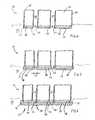
- FIGS. 1-8are diagrammatic cross-sectional views of a fragment of a semiconductor substrate at sequential processing steps showing fabrication of a conductive contact according to an embodiment of the method of the invention.
- FIG. 1illustrates a processing step forming a metal layer on a surface of the substrate.
- FIG. 2shows formation of openings through the substrate and the metal layer.
- FIG. 3shows formation of an isolation layer on the sidewalls of the openings and the surface of the substrate.
- FIGS. 4-6depict sequential processing steps to electroless plate a conductive metal in the gap in the metal layer.
- FIGS. 7-8illustrate sequential electroplating process steps to deposit metal in the opening to form the conductive contact.
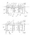
- FIG. 9illustrates in another embodiment of an electroplating process step to fill multiple openings in the substrate according to the invention.
- FIG. 10illustrates another embodiment of a process step to fill the via opening according to the invention, using an electroless plating technique to form the conductive contacts.
- FIG. 11is a cross-sectional view of the wafer fragment after formation of conductive contacts and processing steps to remove excess metal and form circuit traces on the substrate.
- FIG. 12is a block diagram of an embodiment of a system in which the conductive through-vias of the invention can be used.
- the terms “semiconductive wafer fragment” or “wafer fragment” or “wafer”will be understood to mean any construction comprising semiconductor material, including but not limited to bulk semiconductive materials such as a semiconductor wafer (either alone or in assemblies comprising other materials thereon), and semiconductive material layers (either alone or in assemblies comprising other materials).
- substraterefers to any supporting structure including, but not limited to, the semiconductive wafer fragments or wafers described above, and interposer substrates, among others.
- FIGS. 1-8Steps in an embodiment of a method for fabricating a conductive through-via in a semiconductor device 10 according to the invention are illustrated in FIGS. 1-8.
- a substrate 12comprising opposing first and second surfaces 14 , 16 , and a thickness t 1 is provided.
- the substrate 12can comprise an unprocessed semiconductor wafer or other substrate, the wafer with various process layers formed thereon including one or more semiconductor layers or other formations and active or operable portions of semiconductor devices fabricated through etching, deposition, or other well known techniques, an interposer substrate for use between a test substrate and a semiconductor device to be tested or between a memory device and system in a package to provide routing, among other substrates.
- An exemplary thickness t 1 of the substrateis about 28 mil, which can be about 8 to about 32 mil.
- the substrate 12comprises a semiconductive material such as monocrystalline silicon, polycrystalline silicon, germanium, silicon-on-glass, or silicon-on-sapphire, for example, but can also comprises a non-conductive (electrically insulating) material such as a ceramic, a plastic or polymer material such as bismaleimide triazine (BT) resin, a glass filled epoxy resin material such as such as FR-4 or FR-5 laminates, and an aramid-filled resin, for example, among other materials that are used as substrates in fabricating semiconductor devices and carrier substrates.
- a semiconductive materialsuch as monocrystalline silicon, polycrystalline silicon, germanium, silicon-on-glass, or silicon-on-sapphire
- a non-conductive (electrically insulating) materialsuch as a ceramic, a plastic or polymer material such as bismaleimide triazine (BT) resin, a glass filled epoxy resin material such as such as FR-4 or FR-5 laminates, and an aramid-filled resin, for example, among other materials that are
- a layer 18 of conductive metalis applied onto the second surface 16 of the substrate 12 .
- the conductive metal layer 18can comprise nickel, copper, aluminum, palladium, platinum, or silver, for example.
- the metal layer 18can be fabricated by known metallization techniques, such as by chemical vapor deposition (CVD), physical vapor deposition (PVD) (e.g., sputtering), evaporation using a conventional metal evaporator, electroless plating, and electroplating, for example, to deposit a blanket layer of metal over the substrate.
- CVDchemical vapor deposition
- PVDphysical vapor deposition
- electroless platingelectroless plating
- electroplatingfor example, to deposit a blanket layer of metal over the substrate.
- a pre-fabricated metal sheet or foilcan also be adhered or laminated to the substrate using an adhesive material.
- the metal layerincludes an exposed (bottom) surface 20 and sidewalls 22 .
- one or more contact openings or via holes 24are formed through the entire thickness t 1 , t 2 of the substrate 12 and the metal layer 18 , creating an opening or gap 26 in the metal layer.
- the openings 24can be formed using a variety of fabrication techniques known in the art and appropriate to the substrate, including, for example, a dry etch utilizing photolithographic processing, or photochemical processing.
- the openingscan also be formed using a laser machining (drilling) process, as described, for example, in U.S. Pat. No. 6,400,172 (Akram et al.).
- the openings 24include sidewalls 28 , and generally have a diameter (d) of about 0.17 to about 0.90 ⁇ m, typically less than about 0.40 ⁇ m, with substrates ranging in thickness from about 10 ⁇ m to about 725 ⁇ m, typically about 250 ⁇ m, resulting in an aspect ratio of about 42 to about 1 down to about 0.11 to 1, typically greater than about 6.25.
- a conductive metalis then deposited to fill and seal the gap 26 in the metal layer 18 and short the metal layer together.
- a metal fill or plug layer 32is fabricated by plating a conductive metal onto the sidewalls 22 of the metal layer 18 within the gap 26 using an electroless deposition (i.e., electroless plating, electrochemical deposition) process.
- the process of electroless plating of a metalgenerally comprises dipping the semiconductor element with the exposed metal layer into a solution including at least one inorganic metal salt and at least one agent that reduces the metal salt (reducing agent), wherein the metal selectively bonds or plates on the metal layer to a desired thickness.
- metalis deposited onto the sidewalls (edge, rim) 22 of the metal layer 18 within the gap 26 , and on the exposed surface 20 of the metal layer 18 on the backside 33 of the substrate 12 , by dipping at least the metal layer 18 into an electroless plating solution 34 .
- an electroless plating solution 34Referring to FIGS. 4-5, as the plating progresses, there is a uniform build-up of metal 36 from the plating solution 34 onto the sidewalls 22 of the metal layer 18 resulting in the inward growth (arrows 38 ) of the metal layer 18 to fill the gap 26 and the formation of the plug layer 32 , which effectively seals the gap 26 .
- a conventional electroless plating processcan be used.
- Exemplary metalsinclude copper, nickel, cobalt, palladium, platinum, and silver.
- Electroless plating tools and solutions for electrolessly plating these metalsare known in the art.
- the metal solutioncan comprise nickel chloride and a chemical reducing agent such as sodium hydroxyacetate and sodium hypophosphate at a temperature of about 85° C. to about 90° C.
- the metal solutioncan comprise palladium chloride and a chemical reducing agent such as sodium hypophosphate at a temperature of about 50° C. to about 60° C.
- the solutioncan comprise a silver salt such as AgNO 3 or KAg(CN) 2 , and a chemical reducing agent such as potassium hypophosphite, among others.
- the thickness of the plug layer 32 within the gap 26is controlled by the concentration of the metal plating solution 34 and the length of time that the metal layer 18 , 36 is immersed in the aqueous solution 34 . To terminate the electroless deposition, the metal layer is removed and rinsed.
- Electroplating and electroless plating tools and plating solutionsare known in the art and commercially available.
- an electrode 50is placed into contact with the surface 42 of the metal layer 36 , and the front side 52 of the substrate 10 is immersed into an electroplating solution 54 .
- a current from an energy source 56for example, a battery, is applied through the electrode 50 to the metal layer 36 , and metal deposits from solution onto the metal plug layer 32 within the opening 24 to form a metal layer 58 .
- the metalplates upward from the plug layer 32 in the direction of arrow 60 to fill the opening 24 , resulting in the conductive metal contact 40 shown in FIG. 8.
- the current to the electrode 50is then terminated.
- the metal fill 40 within the openings 24can be deposited by an electroless plating process, as described hereinabove.
- the backside of the substrate and metal layer 36can be sealed within a container 44 as described with reference to FIG. 7, without an electrode contact 50 against the metal layer 36 .
- the sealed container-substrate unit 62 (without electrode 50 )can then be submersed into an electroless plating solution for a time period effective to plate a metal layer 58 onto the plug layer 32 and fill the opening 24 to form the contact 40 .
- Platingcan be readily conducted in batch by immersing multiple units 62 (without electrode) into the plating solution.
- a flexible tape or other cover material 64 ′′can be applied to seal the surface 42 ′′ of the metal layer 36 ′′ from contact with the electroless plating solution 34 ′′.
- the taped substratecan be submerged in the plating bath 34 ′′ whereupon metal 58 ′′ from the solution will plate onto exposed surfaces 42 ′′ of the metal layer, including the plug layer 32 ′′ to fill the opening 24 ′′ and form the conductive contacts 40 ′′.
- the device 10is removed from the bath, and excess of the metal fill can be removed according to known methods in the art. Unwanted surface metal can be removed to expose the isolation layer 30 while leaving the desired metal within the opening 24 as depicted. Exemplary methods of removing metal material include a conventional dry etch or chemical mechanical polishing (CMP).
- CMPchemical mechanical polishing
- circuit traces 66 or other interconnects and contact structurescan be fabricated on the isolation layer 30 to couple the via contact 40 to contact pads 68 or other conductive structures, and/or to circuit devices such as a internal circuitry and/or a microprocessor, for example.
- the metal layers 18 , 36 on the backside of the substrate 12can be removed by CMP, etching or other process, or patterned as shown to define circuit traces 70 leading from the via contact 40 to contact pads 72 , as shown.
- the conductive contacts 40can thus connect contact pads 68 on the top surface 14 of the substrate 12 to a conductive element shown as a contact pad 72 on the bottom surface 16 of the substrate.
- the substrate 12can be designed as an interposer for connecting semiconductor devices, including flip-chips, chip scale packages and ball grid array packages to a substrate, such as a test substrate or a higher level carrier substrate.
- the contact pads 68 , 72 on the interposer substratecan be arranged in a pattern that corresponds to that of contact pads on a test or carrier substrate to be connected, or arranged in a different pattern than the bond pads and, therefore, reroute the bond pads of the test or carrier substrate.
- FIG. 12illustrates an embodiment of a system 74 in which the present invention can be incorporated.
- the systemincludes a memory device 76 (e.g., static random access memory (SRAM), dynamic random access memory (DRAM), etc.) comprising a conductive contact according to the invention.
- the memory device 76is coupled to a microprocessor 78 , which may be programmed to carry out particular functions as is known in the art.
Landscapes
- Engineering & Computer Science (AREA)
- Microelectronics & Electronic Packaging (AREA)
- Manufacturing & Machinery (AREA)
- Physics & Mathematics (AREA)
- Condensed Matter Physics & Semiconductors (AREA)
- General Physics & Mathematics (AREA)
- Computer Hardware Design (AREA)
- Power Engineering (AREA)
- Ceramic Engineering (AREA)
- Internal Circuitry In Semiconductor Integrated Circuit Devices (AREA)
Abstract
Description
- The invention relates generally to semiconductor fabrication, and more particularly to methods for providing interconnects from one surface to the opposite surface of a substrate for making electrical connections with semiconductor components, and more particularly to methods for filling a through-via in a wafer, interposer or other substrate with a conductive material.[0001]
- Interposers are utilized for interfacing two electrical components, for example, a semiconductor device and a printed circuit board, or a semiconductor wafer and a probe card for testing of the dies on the wafer. These interposers may comprise silicon or ceramic substrate that include metal-filled vias that extend through the interposer from one side to the opposite side. The metal-filled via provide electrical communication between conductive structures disposed on the opposing surfaces of the interposer, which align with contact pads or other structures of the electrical components to establish electrical connection between the two components.[0002]
- Continued miniaturization of integrated circuits results in contact vias having increasingly higher aspect ratios (defined as the ratio of height to width of the via).[0003]
- Conventional methods of filling a through-via using a plasma chemical vapor deposition (PCVD) process to form a seed layer followed by a conformal metal electroplating process are limited to low aspect ratio openings. As is known in the art, high aspect ratio vias are difficult to fill conformally, that is, without forming voids or keyholes that can adversely affect conductivity of the contacts.[0004]
- The present invention provides methods for fabricating a conductive contact (through-via) through the full thickness of a semiconductor wafer, interposer, or other substrate, and semiconductor devices and systems incorporating the conductive through-via.[0005]
- One embodiment of a method of forming a conductive contact according to the invention comprises applying a layer of metal onto a first surface of a substrate, forming an opening through the substrate and the metal layer, electroless plating a metal to fill the opening through the metal layer, and plating a metal to fill the opening in the substrate. The metal layer can be applied to the backside surface of the substrate by various processes including deposition processes, adhering a metal sheet, among others. The gap formed in the metal layer is sealed by an electroless plating process, and the opening in the substrate is filled with metal deposited by an electroplating or electroless plating process. In embodiments in which the substrate is a semiconductive material (e.g., silicon), an isolation layer can be formed onto sidewalls of the substrate within the opening prior to the metal plating steps. The process of the invention results in a conductive contact that is without voids or keyholes.[0006]
- In another aspect, the invention provides a semiconductor device. In various embodiments, the device comprises a conductive through-via according to the invention disposed through a substrate.[0007]
- In one embodiment, the device comprises the conductive through-via in process, which comprises a layer of metal disposed on a surface of a substrate and an opening through the substrate and the metal layer. In another embodiment, the device comprises a metal layer disposed on a surface of a substrate, an opening through the substrate and the metal layer, and a plated metal disposed in the opening of the metal layer. In yet another embodiment, the device comprises a metal layer disposed on a surface of a substrate, an opening through the substrate and the metal layer, an electrolessly plated metal sealing in the opening (gap) in the metal layer, and a plated metal fill disposed in the opening in the substrate to form a conductive contact.[0008]
- The device can comprise a semiconductor wafer, an interposer, or other substrate comprising the conductive through-via, or the conductive through-via in process.[0009]
- Another aspect of the invention is a system comprising a microprocessor in communication with a memory device comprising the conductive through-via of the invention.[0010]
- The invention advantageously provides a simplified method of forming through-wafer vias that are void-free. The present method involves fewer process steps than prior art methods, provides a cost savings in the production. Additionally, the process achieves a solid fill contact by depositing metal upward from the base of the opening rather than by conformal plating or deposition by vapor.[0011]
- Preferred embodiments of the invention are described below with reference to the following accompanying drawings, which are for illustrative purposes only. Throughout the following views, the reference numerals will be used in the drawings, and the same reference numerals will be used throughout the several views and in the description to indicate same or like parts.[0012]
- FIGS. 1-8 are diagrammatic cross-sectional views of a fragment of a semiconductor substrate at sequential processing steps showing fabrication of a conductive contact according to an embodiment of the method of the invention. FIG. 1 illustrates a processing step forming a metal layer on a surface of the substrate. FIG. 2 shows formation of openings through the substrate and the metal layer. FIG. 3 shows formation of an isolation layer on the sidewalls of the openings and the surface of the substrate. FIGS. 4-6 depict sequential processing steps to electroless plate a conductive metal in the gap in the metal layer. FIGS. 7-8 illustrate sequential electroplating process steps to deposit metal in the opening to form the conductive contact.[0013]
- FIG. 9 illustrates in another embodiment of an electroplating process step to fill multiple openings in the substrate according to the invention.[0014]
- FIG. 10 illustrates another embodiment of a process step to fill the via opening according to the invention, using an electroless plating technique to form the conductive contacts.[0015]
- FIG. 11 is a cross-sectional view of the wafer fragment after formation of conductive contacts and processing steps to remove excess metal and form circuit traces on the substrate.[0016]
- FIG. 12 is a block diagram of an embodiment of a system in which the conductive through-vias of the invention can be used.[0017]
- The invention will be described generally with reference to the drawings for the purpose of illustrating the present preferred embodiments only and not for purposes of limiting the same. The figures illustrate processing steps for use in fabricating a conductive through-via in accordance with the present invention. It should be readily apparent that the processing steps are only a portion of the entire fabrication process.[0018]
- In the current application, the terms “semiconductive wafer fragment” or “wafer fragment” or “wafer” will be understood to mean any construction comprising semiconductor material, including but not limited to bulk semiconductive materials such as a semiconductor wafer (either alone or in assemblies comprising other materials thereon), and semiconductive material layers (either alone or in assemblies comprising other materials). The term “substrate” refers to any supporting structure including, but not limited to, the semiconductive wafer fragments or wafers described above, and interposer substrates, among others.[0019]
- The invention provides methods for filling a through-via that is formed through the thickness of a wafer or other substrate with a conductive metal. The conductive via is disposed in a substrate comprising an opening extending from the first surface to the second surface and at least partially filled with a conductive material. The conductive vias can be used for interconnecting contacts on a component, for example, a contact pad on one side of a substrate (e.g., interposer) to a conductive element such as a contact pad on the opposing side of the substrate, among other uses.[0020]
- Steps in an embodiment of a method for fabricating a conductive through-via in a[0021]
semiconductor device 10 according to the invention are illustrated in FIGS. 1-8. Initially, as shown in FIG. 1, asubstrate 12 comprising opposing first andsecond surfaces substrate 12 can comprise an unprocessed semiconductor wafer or other substrate, the wafer with various process layers formed thereon including one or more semiconductor layers or other formations and active or operable portions of semiconductor devices fabricated through etching, deposition, or other well known techniques, an interposer substrate for use between a test substrate and a semiconductor device to be tested or between a memory device and system in a package to provide routing, among other substrates. An exemplary thickness t1of the substrate is about 28 mil, which can be about 8 to about 32 mil. - In the illustrated example, the[0022]
substrate 12 comprises a semiconductive material such as monocrystalline silicon, polycrystalline silicon, germanium, silicon-on-glass, or silicon-on-sapphire, for example, but can also comprises a non-conductive (electrically insulating) material such as a ceramic, a plastic or polymer material such as bismaleimide triazine (BT) resin, a glass filled epoxy resin material such as such as FR-4 or FR-5 laminates, and an aramid-filled resin, for example, among other materials that are used as substrates in fabricating semiconductor devices and carrier substrates. - As shown in FIG. 1, a[0023]
layer 18 of conductive metal is applied onto thesecond surface 16 of thesubstrate 12. Theconductive metal layer 18 can comprise nickel, copper, aluminum, palladium, platinum, or silver, for example. Themetal layer 18 can be fabricated by known metallization techniques, such as by chemical vapor deposition (CVD), physical vapor deposition (PVD) (e.g., sputtering), evaporation using a conventional metal evaporator, electroless plating, and electroplating, for example, to deposit a blanket layer of metal over the substrate. A pre-fabricated metal sheet or foil can also be adhered or laminated to the substrate using an adhesive material. As depicted, the metal layer includes an exposed (bottom)surface 20 andsidewalls 22. - The thickness t[0024]2of the
metal layer 18 can range from a thin seed layer of about 0.2 to about 0.5 μm to a thicker layer of up to about 2 μm. Preferably, the thickness t2of themetal layer 18 is about one-tenth of the radius (r1) of thegap 26 that is subsequently formed in the metal layer18 (FIG. 2). - Next, as shown in FIG. 2, one or more contact openings or via[0025]
holes 24 are formed through the entire thickness t1, t2of thesubstrate 12 and themetal layer 18, creating an opening orgap 26 in the metal layer. Theopenings 24 can be formed using a variety of fabrication techniques known in the art and appropriate to the substrate, including, for example, a dry etch utilizing photolithographic processing, or photochemical processing. The openings can also be formed using a laser machining (drilling) process, as described, for example, in U.S. Pat. No. 6,400,172 (Akram et al.). Theopenings 24 includesidewalls 28, and generally have a diameter (d) of about 0.17 to about 0.90 μm, typically less than about 0.40 μm, with substrates ranging in thickness from about 10 μm to about 725 μm, typically about 250 μm, resulting in an aspect ratio of about 42 to about 1 down to about 0.11 to 1, typically greater than about 6.25. - Following formation of the[0026]
openings 18, a clean step can be performed to remove residual materials from the openings. Such a clean step can be performed, for example, by wet etching or stripping a sacrificial layer. - As shown in FIG. 3, an[0027]
isolation layer 30 can be formed on thesidewalls 28 within theopenings 24 and on thefirst surface 12 of thesubstrate 12 by known techniques in the art. Theisolation layer 30 can comprise a dielectric or insulative material such as an oxide (e.g., silicon dioxide (SiO2)), nitride (e.g., silicon nitride (Si3N4)), or an oxynitride, for example, or a glass such as borophosphosilicate glass (BPSG), phosphosilicate glass (PSG), or borosilicate glass (BSG). The isolation layer can be formed to a desired thickness using, chemical vapor deposition (CVD), low pressure chemical vapor deposition (LPCVD), rapid thermal nitridation (RTN), spin-on-glass (SOG) process, flow coating, or other process. Theisolation layer 30 can also comprise an insulating polymer, such as BT resin, polyimide, benzocyclobutene (BCB), and/or polybenzoxazole (PBO), for example, deposited using an injection or capillary process or vacuum draw. A representative thickness of the isolation layer is about 1-5 μm. If thesubstrate 12 is formed of an electrically insulating material (e.g., ceramic), the isolation layer can be eliminated. - As shown in FIGS. 4-6, a conductive metal is then deposited to fill and seal the[0028]
gap 26 in themetal layer 18 and short the metal layer together. According to the invention, a metal fill or pluglayer 32 is fabricated by plating a conductive metal onto thesidewalls 22 of themetal layer 18 within thegap 26 using an electroless deposition (i.e., electroless plating, electrochemical deposition) process. The process of electroless plating of a metal generally comprises dipping the semiconductor element with the exposed metal layer into a solution including at least one inorganic metal salt and at least one agent that reduces the metal salt (reducing agent), wherein the metal selectively bonds or plates on the metal layer to a desired thickness. - Using an electroless deposition process, metal is deposited onto the sidewalls (edge, rim)[0029]22 of the
metal layer 18 within thegap 26, and on the exposedsurface 20 of themetal layer 18 on thebackside 33 of thesubstrate 12, by dipping at least themetal layer 18 into anelectroless plating solution 34. Referring to FIGS. 4-5, as the plating progresses, there is a uniform build-up ofmetal 36 from theplating solution 34 onto thesidewalls 22 of themetal layer 18 resulting in the inward growth (arrows38) of themetal layer 18 to fill thegap 26 and the formation of theplug layer 32, which effectively seals thegap 26. There is a corresponding build-up ofmetal 36 onto the exposed (bottom) surface20 of themetal layer 18 on thebackside 33 of thesubstrate 12. - For example, a[0030]
metal layer 18 having a thickness t2of about 2 μm can be applied onto thesurface 16 of thesubstrate 12, and acontact opening 24 can be formed in the substrate through themetal layer 18 forming agap 26 having a diameter d1of about 50 μm (or radius r1of about 25 μm). Plating can then be performed, whereby a buildup ofmetal 36 to a thickness of about 25 μm on the exposed surfaces20 (including the sidewalls22) of themetal layer 18 will form aplug 32 to fill the gap26 (FIG. 6), and increase the thickness t2of themetal layer 18 on thebackside 33 of thesubstrate 12 to about 27 μm (about the radius r1). - A conventional electroless plating process can be used. Exemplary metals include copper, nickel, cobalt, palladium, platinum, and silver. Electroless plating tools and solutions for electrolessly plating these metals are known in the art. For example, for electroless depositing nickel, the metal solution can comprise nickel chloride and a chemical reducing agent such as sodium hydroxyacetate and sodium hypophosphate at a temperature of about 85° C. to about 90° C. For depositing palladium, the metal solution can comprise palladium chloride and a chemical reducing agent such as sodium hypophosphate at a temperature of about 50° C. to about 60° C. For depositing silver, the solution can comprise a silver salt such as AgNO[0031]3or KAg(CN)2, and a chemical reducing agent such as potassium hypophosphite, among others.
- The thickness of the[0032]
plug layer 32 within thegap 26 is controlled by the concentration of themetal plating solution 34 and the length of time that themetal layer aqueous solution 34. To terminate the electroless deposition, the metal layer is removed and rinsed. - Next, a conventional electroplating or electroless plating process is used to deposit a conductive metal into the[0033]
openings 24 onto theplug layer 32 to fill theopening 24 and form aconductive contact 40. Electroplating and electroless plating tools and plating solutions are known in the art and commercially available. - Generally, in an electroplating process, a substrate is submerged in a plating bath comprising metal ions. A current is applied to reduce the metal ions within the plating solution and metal deposits onto exposed metal surfaces on the substrate. The substrate remains submerged in the solution bath and the current is applied until a desired thickness of metal is deposited. The current is then terminated and the substrate is placed into a rinse bath to remove residual bath liquid and particles from the surface.[0034]
- In an electroplating process according to the invention, the exposed[0035]
surface 42 of themetal layer 36 on thebackside 33 of thesubstrate 12 is sealed or covered to prevent further metal deposition thereon, and theopenings 24 are uncovered. For example, as depicted in FIG. 7, thesubstrate 12 can be housed within acontainer 44 with sealing members46 (e.g., rubber seals) disposed on the insulatinglayer 30 over the first (front side) surface14 of thesubstrate 12, with theopenings 24 exposed. As shown, a volume ofgas 48 such as air or nitrogen (N2) is disposed within thecontainer 44 aboutmetal layer 36 on thebackside 33 of thesubstrate 12. According to the method, anelectrode 50 is placed into contact with thesurface 42 of themetal layer 36, and thefront side 52 of thesubstrate 10 is immersed into anelectroplating solution 54. A current from anenergy source 56, for example, a battery, is applied through theelectrode 50 to themetal layer 36, and metal deposits from solution onto themetal plug layer 32 within theopening 24 to form ametal layer 58. The metal plates upward from theplug layer 32 in the direction ofarrow 60 to fill theopening 24, resulting in theconductive metal contact 40 shown in FIG. 8. The current to theelectrode 50 is then terminated. - FIG. 9 illustrates another embodiment of an electroplating process to fill multiple openings in the substrate. As shown, a[0036]
blanket electrode 50′ (metal sheet, bus bar) can be positioned over thesurface 42′ of themetal layer 36′. A current from theelectrode 50′ to theplug layer 32′ causes metal from theplating solution 54′ to deposit onto the plug layers32′ in each of theopenings 24′ to form theconductive contacts 40′. - Electroplating solutions are known and commercially available. The solution can comprise a conventional electroplating solution, including a metal sulfate solution and acids, commercially available, for example, from Shipley Company, LLC of Marlborough, Mass., Pac Tech USA, Inc. of Santa Clara, Calif., or Enthone OMI (Ethone, Inc., West Haven, Conn.). For example, in a copper electroplating process, the solution can comprise copper sulfate. In an example of a silver electroplating process, the substrate is immersed in a bath comprising a commercially available silver plating bath, for example, a cyanide-free silver plating solution comprising silver succinimide (C[0037]4H5O2NAg), commercially under the trade name Techni-Silver CY-LESS® L2 from Technic, Inc., Cranston, R.I.
- In another embodiment, the metal fill[0038]40 within the
openings 24 can be deposited by an electroless plating process, as described hereinabove. For example, the backside of the substrate andmetal layer 36 can be sealed within acontainer 44 as described with reference to FIG. 7, without anelectrode contact 50 against themetal layer 36. The sealed container-substrate unit62 (without electrode50) can then be submersed into an electroless plating solution for a time period effective to plate ametal layer 58 onto theplug layer 32 and fill theopening 24 to form thecontact 40. Plating can be readily conducted in batch by immersing multiple units62 (without electrode) into the plating solution. - In another example of an electroless plating process shown in FIG. 10, a flexible tape or[0039]
other cover material 64″ can be applied to seal thesurface 42″ of themetal layer 36″ from contact with theelectroless plating solution 34″. The taped substrate can be submerged in theplating bath 34″ whereuponmetal 58″ from the solution will plate onto exposedsurfaces 42″ of the metal layer, including theplug layer 32″ to fill theopening 24″ and form theconductive contacts 40″. - Referring now to FIG. 11, after formation of the[0040]
contacts 40, thedevice 10 is removed from the bath, and excess of the metal fill can be removed according to known methods in the art. Unwanted surface metal can be removed to expose theisolation layer 30 while leaving the desired metal within theopening 24 as depicted. Exemplary methods of removing metal material include a conventional dry etch or chemical mechanical polishing (CMP). The finished construction includes aconductive contact 40 formed within theopening 24. - Optionally, as also depicted, circuit traces[0041]66 or other interconnects and contact structures can be fabricated on the
isolation layer 30 to couple the viacontact 40 to contactpads 68 or other conductive structures, and/or to circuit devices such as a internal circuitry and/or a microprocessor, for example. In addition, the metal layers18,36 on the backside of thesubstrate 12 can be removed by CMP, etching or other process, or patterned as shown to define circuit traces70 leading from the viacontact 40 to contactpads 72, as shown. Theconductive contacts 40 can thus connectcontact pads 68 on thetop surface 14 of thesubstrate 12 to a conductive element shown as acontact pad 72 on thebottom surface 16 of the substrate. - The[0042]
substrate 12 can be designed as an interposer for connecting semiconductor devices, including flip-chips, chip scale packages and ball grid array packages to a substrate, such as a test substrate or a higher level carrier substrate. Thecontact pads - Subsequent processing may then be conducted on[0043]
semiconductor device structure 10, as known in the art. - FIG. 12 illustrates an embodiment of a[0044]
system 74 in which the present invention can be incorporated. The system includes a memory device76 (e.g., static random access memory (SRAM), dynamic random access memory (DRAM), etc.) comprising a conductive contact according to the invention. Thememory device 76 is coupled to amicroprocessor 78, which may be programmed to carry out particular functions as is known in the art. - In compliance with the statute, the invention has been described in language more or less specific as to structural and methodical features. It is to be understood, however, that the invention is not limited to the specific features shown and described, since the means herein disclosed comprise preferred forms of putting the invention into effect. The invention is, therefore, claimed in any of its forms or modifications within the proper scope of the appended claims appropriately interpreted in accordance with the doctrine of equivalents.[0045]
Claims (100)
Priority Applications (2)
| Application Number | Priority Date | Filing Date | Title |
|---|---|---|---|
| US10/379,890US6852627B2 (en) | 2003-03-05 | 2003-03-05 | Conductive through wafer vias |
| US11/052,181US20050200027A1 (en) | 2003-03-05 | 2005-02-07 | Conductive through wafer vias |
Applications Claiming Priority (1)
| Application Number | Priority Date | Filing Date | Title |
|---|---|---|---|
| US10/379,890US6852627B2 (en) | 2003-03-05 | 2003-03-05 | Conductive through wafer vias |
Related Child Applications (1)
| Application Number | Title | Priority Date | Filing Date |
|---|---|---|---|
| US11/052,181DivisionUS20050200027A1 (en) | 2003-03-05 | 2005-02-07 | Conductive through wafer vias |
Publications (2)
| Publication Number | Publication Date |
|---|---|
| US20040173909A1true US20040173909A1 (en) | 2004-09-09 |
| US6852627B2 US6852627B2 (en) | 2005-02-08 |
Family
ID=32926779
Family Applications (2)
| Application Number | Title | Priority Date | Filing Date |
|---|---|---|---|
| US10/379,890Expired - LifetimeUS6852627B2 (en) | 2003-03-05 | 2003-03-05 | Conductive through wafer vias |
| US11/052,181AbandonedUS20050200027A1 (en) | 2003-03-05 | 2005-02-07 | Conductive through wafer vias |
Family Applications After (1)
| Application Number | Title | Priority Date | Filing Date |
|---|---|---|---|
| US11/052,181AbandonedUS20050200027A1 (en) | 2003-03-05 | 2005-02-07 | Conductive through wafer vias |
Country Status (1)
| Country | Link |
|---|---|
| US (2) | US6852627B2 (en) |
Cited By (19)
| Publication number | Priority date | Publication date | Assignee | Title |
|---|---|---|---|---|
| US20070222066A1 (en)* | 2006-03-24 | 2007-09-27 | International Business Machines Corporation | Structure and method of forming electrodeposited contacts |
| US20080206984A1 (en)* | 2007-02-27 | 2008-08-28 | Sparks Terry G | Conductive via formation utilizing electroplating |
| US20080217784A1 (en)* | 2006-10-20 | 2008-09-11 | Florian Binder | Substrate with feedthrough and method for producing the same |
| WO2008087578A3 (en)* | 2007-01-17 | 2008-09-12 | Nxp Bv | A system-in-package with through substrate via holes |
| US20090008747A1 (en)* | 2007-07-02 | 2009-01-08 | Masataka Hoshino | Semiconductor device and method for manufacturing thereof |
| US20090081867A1 (en)* | 2007-09-21 | 2009-03-26 | Shinko Electric Industries Co., Ltd. | Method of manufacturing substrate |
| US7589009B1 (en)* | 2006-10-02 | 2009-09-15 | Newport Fab, Llc | Method for fabricating a top conductive layer in a semiconductor die and related structure |
| WO2010041165A1 (en)* | 2008-10-10 | 2010-04-15 | Nxp B.V. | Method of plating through wafer vias in a wafer for 3d packaging |
| US20120080318A1 (en)* | 2010-10-04 | 2012-04-05 | Gillen James R | Forming Through-Substrate Vias by Electrofilling |
| US20130313122A1 (en)* | 2012-05-24 | 2013-11-28 | Viking Tech Corporation | Method For Fabricating Conductive Structures of Substrate |
| US8809189B2 (en) | 2012-01-13 | 2014-08-19 | Samsung Electronics Co., Ltd. | Method of forming through-silicon via using laser ablation |
| US9287207B2 (en) | 2003-09-23 | 2016-03-15 | Micron Technology, Inc. | Methods for forming conductive vias in semiconductor device components |
| WO2016194241A1 (en)* | 2015-05-31 | 2016-12-08 | 清川メッキ工業株式会社 | Method for manufacturing wiring board |
| US9756736B2 (en) | 2015-05-31 | 2017-09-05 | Kiyokawa Plating Industry Co., Ltd | Process for producing a wiring board |
| CN110634792A (en)* | 2019-09-26 | 2019-12-31 | 上海航天电子通讯设备研究所 | Method for manufacturing electric interconnection substrate |
| US10699954B2 (en) | 2018-04-19 | 2020-06-30 | Teledyne Scientific & Imaging, Llc | Through-substrate vias formed by bottom-up electroplating |
| CN111739870A (en)* | 2020-07-10 | 2020-10-02 | 电子科技大学 | High polymer buffer layer copper coaxial TGV, adapter plate and preparation method thereof |
| CN112289821A (en)* | 2016-04-14 | 2021-01-29 | 群创光电股份有限公司 | Display device |
| USRE49390E1 (en)* | 2009-02-05 | 2023-01-24 | Longitude Licensing Limited | Testing a circuit in a semiconductor device |
Families Citing this family (38)
| Publication number | Priority date | Publication date | Assignee | Title |
|---|---|---|---|---|
| GB0312917D0 (en)* | 2003-06-05 | 2003-07-09 | Ici Plc | Materials testing |
| CN100512603C (en)* | 2003-09-09 | 2009-07-08 | Hoya株式会社 | Method for manufacturing double-sided printed glass board |
| US7101792B2 (en)* | 2003-10-09 | 2006-09-05 | Micron Technology, Inc. | Methods of plating via interconnects |
| US7316063B2 (en)* | 2004-01-12 | 2008-01-08 | Micron Technology, Inc. | Methods of fabricating substrates including at least one conductive via |
| SG135065A1 (en) | 2006-02-20 | 2007-09-28 | Micron Technology Inc | Conductive vias having two or more elements for providing communication between traces in different substrate planes, semiconductor device assemblies including such vias, and accompanying methods |
| US7129567B2 (en)* | 2004-08-31 | 2006-10-31 | Micron Technology, Inc. | Substrate, semiconductor die, multichip module, and system including a via structure comprising a plurality of conductive elements |
| US7538032B2 (en)* | 2005-06-23 | 2009-05-26 | Teledyne Scientific & Imaging, Llc | Low temperature method for fabricating high-aspect ratio vias and devices fabricated by said method |
| JP4688526B2 (en)* | 2005-03-03 | 2011-05-25 | Okiセミコンダクタ株式会社 | Semiconductor device and manufacturing method thereof |
| US20060252254A1 (en)* | 2005-05-06 | 2006-11-09 | Basol Bulent M | Filling deep and wide openings with defect-free conductor |
| JP4533283B2 (en)* | 2005-08-29 | 2010-09-01 | 新光電気工業株式会社 | Manufacturing method of semiconductor device |
| US7633167B2 (en)* | 2005-09-29 | 2009-12-15 | Nec Electronics Corporation | Semiconductor device and method for manufacturing same |
| JP2007150176A (en)* | 2005-11-30 | 2007-06-14 | Sharp Corp | Semiconductor device and manufacturing method thereof |
| US7589390B2 (en)* | 2006-03-10 | 2009-09-15 | Teledyne Technologies, Incorporated | Shielded through-via |
| US7485561B2 (en)* | 2006-03-29 | 2009-02-03 | Asm Nutool, Inc. | Filling deep features with conductors in semiconductor manufacturing |
| US7625814B2 (en)* | 2006-03-29 | 2009-12-01 | Asm Nutool, Inc. | Filling deep features with conductors in semiconductor manufacturing |
| US7626269B2 (en)* | 2006-07-06 | 2009-12-01 | Micron Technology, Inc. | Semiconductor constructions and assemblies, and electronic systems |
| US7989915B2 (en)* | 2006-07-11 | 2011-08-02 | Teledyne Licensing, Llc | Vertical electrical device |
| US7560371B2 (en)* | 2006-08-29 | 2009-07-14 | Micron Technology, Inc. | Methods for selectively filling apertures in a substrate to form conductive vias with a liquid using a vacuum |
| JP5117698B2 (en)* | 2006-09-27 | 2013-01-16 | ルネサスエレクトロニクス株式会社 | Semiconductor device |
| US20080237048A1 (en)* | 2007-03-30 | 2008-10-02 | Ismail Emesh | Method and apparatus for selective electrofilling of through-wafer vias |
| US7829462B2 (en)* | 2007-05-03 | 2010-11-09 | Teledyne Licensing, Llc | Through-wafer vias |
| US8003517B2 (en)* | 2007-05-29 | 2011-08-23 | Freescale Semiconductor, Inc. | Method for forming interconnects for 3-D applications |
| KR100907896B1 (en)* | 2007-06-22 | 2009-07-14 | 주식회사 동부하이텍 | How to Form Metal Electrodes in System-in-Package |
| US20090065365A1 (en)* | 2007-09-11 | 2009-03-12 | Asm Nutool, Inc. | Method and apparatus for copper electroplating |
| KR20100126714A (en)* | 2008-01-30 | 2010-12-02 | 이노벤트 테크놀로지스, 엘엘씨 | Method and apparatus for manufacturing via disk |
| US7898063B2 (en)* | 2008-02-16 | 2011-03-01 | International Business Machines Corporation | Through substrate annular via including plug filler |
| US7821107B2 (en) | 2008-04-22 | 2010-10-26 | Micron Technology, Inc. | Die stacking with an annular via having a recessed socket |
| US20100001378A1 (en)* | 2008-07-01 | 2010-01-07 | Teledyne Scientific & Imaging, Llc | Through-substrate vias and method of fabricating same |
| US8187972B2 (en) | 2008-07-01 | 2012-05-29 | Teledyne Scientific & Imaging, Llc | Through-substrate vias with polymer fill and method of fabricating same |
| US8088667B2 (en)* | 2008-11-05 | 2012-01-03 | Teledyne Scientific & Imaging, Llc | Method of fabricating vertical capacitors in through-substrate vias |
| US7884016B2 (en)* | 2009-02-12 | 2011-02-08 | Asm International, N.V. | Liner materials and related processes for 3-D integration |
| US8754507B2 (en) | 2011-01-18 | 2014-06-17 | Hong Kong Applied Science and Technology Research Institute Company Limited | Forming through-silicon-vias for multi-wafer integrated circuits |
| JP2014060185A (en) | 2012-09-14 | 2014-04-03 | Toshiba Corp | Semiconductor device manufacturing method and semiconductor device |
| US10593562B2 (en) | 2015-04-02 | 2020-03-17 | Samtec, Inc. | Method for creating through-connected vias and conductors on a substrate |
| US9691634B2 (en) | 2015-04-02 | 2017-06-27 | Abexl Inc. | Method for creating through-connected vias and conductors on a substrate |
| WO2019191621A1 (en) | 2018-03-30 | 2019-10-03 | Samtec, Inc. | Electrically conductive vias and methods for producing same |
| WO2019204207A1 (en)* | 2018-04-18 | 2019-10-24 | Corning Incorporated | Systems and methods for forming direct drive microled displays |
| US12100647B2 (en) | 2019-09-30 | 2024-09-24 | Samtec, Inc. | Electrically conductive vias and methods for producing same |
Citations (23)
| Publication number | Priority date | Publication date | Assignee | Title |
|---|---|---|---|---|
| US80408A (en)* | 1868-07-28 | Joseph g | ||
| US98711A (en)* | 1870-01-11 | Improved hay-tork | ||
| US109233A (en)* | 1870-11-15 | Improvement in devices for delivering mail-bags to cars | ||
| US267822A (en)* | 1882-11-21 | Rolls for rolling shovel-blanks | ||
| US5024966A (en)* | 1988-12-21 | 1991-06-18 | At&T Bell Laboratories | Method of forming a silicon-based semiconductor optical device mount |
| US5949141A (en)* | 1995-12-22 | 1999-09-07 | Micron Technology, Inc. | Laminated film/metal structures |
| US5998292A (en)* | 1997-11-12 | 1999-12-07 | International Business Machines Corporation | Method for making three dimensional circuit integration |
| US6032527A (en)* | 1998-07-01 | 2000-03-07 | Memsys, Inc. | Solid state microanemometer |
| US6221769B1 (en)* | 1999-03-05 | 2001-04-24 | International Business Machines Corporation | Method for integrated circuit power and electrical connections via through-wafer interconnects |
| US6268660B1 (en)* | 1999-03-05 | 2001-07-31 | International Business Machines Corporation | Silicon packaging with through wafer interconnects |
| US6270601B1 (en)* | 1998-11-02 | 2001-08-07 | Coorstek, Inc. | Method for producing filled vias in electronic components |
| US6294837B1 (en)* | 1997-12-18 | 2001-09-25 | Micron Technology, Inc. | Semiconductor interconnect having laser machined contacts |
| US20010024129A1 (en)* | 2000-03-23 | 2001-09-27 | Salman Akram | Interposer and methods for fabricating same |
| US6333555B1 (en)* | 1997-12-12 | 2001-12-25 | Micron Technology, Inc. | Interconnect for semiconductor components and method of fabrication |
| US6359328B1 (en)* | 1998-12-31 | 2002-03-19 | Intel Corporation | Methods for making interconnects and diffusion barriers in integrated circuits |
| US6400172B1 (en)* | 1997-12-18 | 2002-06-04 | Micron Technology, Inc. | Semiconductor components having lasered machined conductive vias |
| US6413862B1 (en)* | 1996-05-21 | 2002-07-02 | Micron Technology, Inc. | Use of palladium in IC manufacturing |
| US20020098711A1 (en)* | 2000-08-31 | 2002-07-25 | Klein Rita J. | Electroless deposition of doped noble metals and noble metal alloys |
| US20020109233A1 (en)* | 2000-01-18 | 2002-08-15 | Micron Technology, Inc. | Process for providing seed layers for integrated circuit metallurgy |
| US6441479B1 (en)* | 2000-03-02 | 2002-08-27 | Micron Technology, Inc. | System-on-a-chip with multi-layered metallized through-hole interconnection |
| US6444110B2 (en)* | 1999-05-17 | 2002-09-03 | Shipley Company, L.L.C. | Electrolytic copper plating method |
| US6465877B1 (en)* | 1997-10-31 | 2002-10-15 | Micron Technology, Inc. | Semiconductor package including flex circuit, interconnects and dense array external contacts |
| US20030080408A1 (en)* | 1997-12-18 | 2003-05-01 | Farnworth Warren M. | Method for fabricating semiconductor components and interconnects with contacts on opposing sides |
Family Cites Families (3)
| Publication number | Priority date | Publication date | Assignee | Title |
|---|---|---|---|---|
| JP2002232135A (en)* | 2001-01-30 | 2002-08-16 | Matsushita Electric Ind Co Ltd | Double-sided circuit board for lamination, method for manufacturing the same, and multilayer printed wiring board using the same |
| US7049528B2 (en)* | 2002-02-06 | 2006-05-23 | Ibiden Co., Ltd. | Semiconductor chip mounting wiring board, manufacturing method for same, and semiconductor module |
| US6936536B2 (en)* | 2002-10-09 | 2005-08-30 | Micron Technology, Inc. | Methods of forming conductive through-wafer vias |
- 2003
- 2003-03-05USUS10/379,890patent/US6852627B2/ennot_activeExpired - Lifetime
- 2005
- 2005-02-07USUS11/052,181patent/US20050200027A1/ennot_activeAbandoned
Patent Citations (24)
| Publication number | Priority date | Publication date | Assignee | Title |
|---|---|---|---|---|
| US80408A (en)* | 1868-07-28 | Joseph g | ||
| US98711A (en)* | 1870-01-11 | Improved hay-tork | ||
| US109233A (en)* | 1870-11-15 | Improvement in devices for delivering mail-bags to cars | ||
| US267822A (en)* | 1882-11-21 | Rolls for rolling shovel-blanks | ||
| US5024966A (en)* | 1988-12-21 | 1991-06-18 | At&T Bell Laboratories | Method of forming a silicon-based semiconductor optical device mount |
| US5949141A (en)* | 1995-12-22 | 1999-09-07 | Micron Technology, Inc. | Laminated film/metal structures |
| US6242103B1 (en)* | 1995-12-22 | 2001-06-05 | Micron Technology, Inc. | Method for producing laminated film/metal structures |
| US6413862B1 (en)* | 1996-05-21 | 2002-07-02 | Micron Technology, Inc. | Use of palladium in IC manufacturing |
| US6465877B1 (en)* | 1997-10-31 | 2002-10-15 | Micron Technology, Inc. | Semiconductor package including flex circuit, interconnects and dense array external contacts |
| US5998292A (en)* | 1997-11-12 | 1999-12-07 | International Business Machines Corporation | Method for making three dimensional circuit integration |
| US6333555B1 (en)* | 1997-12-12 | 2001-12-25 | Micron Technology, Inc. | Interconnect for semiconductor components and method of fabrication |
| US6294837B1 (en)* | 1997-12-18 | 2001-09-25 | Micron Technology, Inc. | Semiconductor interconnect having laser machined contacts |
| US6400172B1 (en)* | 1997-12-18 | 2002-06-04 | Micron Technology, Inc. | Semiconductor components having lasered machined conductive vias |
| US20030080408A1 (en)* | 1997-12-18 | 2003-05-01 | Farnworth Warren M. | Method for fabricating semiconductor components and interconnects with contacts on opposing sides |
| US6032527A (en)* | 1998-07-01 | 2000-03-07 | Memsys, Inc. | Solid state microanemometer |
| US6270601B1 (en)* | 1998-11-02 | 2001-08-07 | Coorstek, Inc. | Method for producing filled vias in electronic components |
| US6359328B1 (en)* | 1998-12-31 | 2002-03-19 | Intel Corporation | Methods for making interconnects and diffusion barriers in integrated circuits |
| US6268660B1 (en)* | 1999-03-05 | 2001-07-31 | International Business Machines Corporation | Silicon packaging with through wafer interconnects |
| US6221769B1 (en)* | 1999-03-05 | 2001-04-24 | International Business Machines Corporation | Method for integrated circuit power and electrical connections via through-wafer interconnects |
| US6444110B2 (en)* | 1999-05-17 | 2002-09-03 | Shipley Company, L.L.C. | Electrolytic copper plating method |
| US20020109233A1 (en)* | 2000-01-18 | 2002-08-15 | Micron Technology, Inc. | Process for providing seed layers for integrated circuit metallurgy |
| US6441479B1 (en)* | 2000-03-02 | 2002-08-27 | Micron Technology, Inc. | System-on-a-chip with multi-layered metallized through-hole interconnection |
| US20010024129A1 (en)* | 2000-03-23 | 2001-09-27 | Salman Akram | Interposer and methods for fabricating same |
| US20020098711A1 (en)* | 2000-08-31 | 2002-07-25 | Klein Rita J. | Electroless deposition of doped noble metals and noble metal alloys |
Cited By (40)
| Publication number | Priority date | Publication date | Assignee | Title |
|---|---|---|---|---|
| US9287207B2 (en) | 2003-09-23 | 2016-03-15 | Micron Technology, Inc. | Methods for forming conductive vias in semiconductor device components |
| US8089157B2 (en) | 2006-03-24 | 2012-01-03 | International Business Machines Corporation | Contact metallurgy structure |
| US7405154B2 (en) | 2006-03-24 | 2008-07-29 | International Business Machines Corporation | Structure and method of forming electrodeposited contacts |
| US20070222066A1 (en)* | 2006-03-24 | 2007-09-27 | International Business Machines Corporation | Structure and method of forming electrodeposited contacts |
| US20110084393A1 (en)* | 2006-03-24 | 2011-04-14 | International Business Machines Corporation | Method of forming electrodeposited contacts |
| US7851357B2 (en) | 2006-03-24 | 2010-12-14 | International Business Machines Corporation | Method of forming electrodeposited contacts |
| US20090014878A1 (en)* | 2006-03-24 | 2009-01-15 | International Business Machines Corporation | Structure and method of forming electrodeposited contacts |
| US7589009B1 (en)* | 2006-10-02 | 2009-09-15 | Newport Fab, Llc | Method for fabricating a top conductive layer in a semiconductor die and related structure |
| US8263491B2 (en)* | 2006-10-20 | 2012-09-11 | Infineon Technologies Ag | Substrate with feedthrough and method for producing the same |
| US20080217784A1 (en)* | 2006-10-20 | 2008-09-11 | Florian Binder | Substrate with feedthrough and method for producing the same |
| US20100044853A1 (en)* | 2007-01-17 | 2010-02-25 | Nxp, B.V. | System-in-package with through substrate via holes |
| WO2008087578A3 (en)* | 2007-01-17 | 2008-09-12 | Nxp Bv | A system-in-package with through substrate via holes |
| US7741218B2 (en)* | 2007-02-27 | 2010-06-22 | Freescale Semiconductor, Inc. | Conductive via formation utilizing electroplating |
| US20080206984A1 (en)* | 2007-02-27 | 2008-08-28 | Sparks Terry G | Conductive via formation utilizing electroplating |
| TWI483312B (en)* | 2007-02-27 | 2015-05-01 | Freescale Semiconductor Inc | Conductive via formation utilizing electroplating |
| US20100276801A1 (en)* | 2007-07-02 | 2010-11-04 | Masataka Hoshino | Semiconductor device and method to manufacture thereof |
| US7786587B2 (en)* | 2007-07-02 | 2010-08-31 | Spansion Llc | Semiconductor device and method for manufacturing thereof |
| US8148771B2 (en) | 2007-07-02 | 2012-04-03 | Spansion Llc | Semiconductor device and method to manufacture thereof |
| US20090008747A1 (en)* | 2007-07-02 | 2009-01-08 | Masataka Hoshino | Semiconductor device and method for manufacturing thereof |
| US20090081867A1 (en)* | 2007-09-21 | 2009-03-26 | Shinko Electric Industries Co., Ltd. | Method of manufacturing substrate |
| US7981798B2 (en)* | 2007-09-21 | 2011-07-19 | Shinko Electric Industries Co., Ltd. | Method of manufacturing substrate |
| CN102246292A (en)* | 2008-10-10 | 2011-11-16 | 台湾积体电路制造股份有限公司 | Method for electroplating through wafer vias in a wafer for 3D packaging |
| WO2010041165A1 (en)* | 2008-10-10 | 2010-04-15 | Nxp B.V. | Method of plating through wafer vias in a wafer for 3d packaging |
| USRE49390E1 (en)* | 2009-02-05 | 2023-01-24 | Longitude Licensing Limited | Testing a circuit in a semiconductor device |
| US20120080318A1 (en)* | 2010-10-04 | 2012-04-05 | Gillen James R | Forming Through-Substrate Vias by Electrofilling |
| US8809189B2 (en) | 2012-01-13 | 2014-08-19 | Samsung Electronics Co., Ltd. | Method of forming through-silicon via using laser ablation |
| CN103429011A (en)* | 2012-05-24 | 2013-12-04 | 光颉科技股份有限公司 | Conduction process method of substrate |
| US20130313122A1 (en)* | 2012-05-24 | 2013-11-28 | Viking Tech Corporation | Method For Fabricating Conductive Structures of Substrate |
| KR101849158B1 (en) | 2015-05-31 | 2018-04-16 | 기요카와 멕키 고교 가부시키가이샤 | Process for producing a wiring board |
| JPWO2016194241A1 (en)* | 2015-05-31 | 2017-12-28 | 清川メッキ工業株式会社 | Wiring substrate manufacturing method |
| KR20180036805A (en)* | 2015-05-31 | 2018-04-09 | 기요카와 멕키 고교 가부시키가이샤 | Process for producing a wiring board |
| US9756736B2 (en) | 2015-05-31 | 2017-09-05 | Kiyokawa Plating Industry Co., Ltd | Process for producing a wiring board |
| CN108738249A (en)* | 2015-05-31 | 2018-11-02 | 清川镀金工业株式会社 | The manufacturing method of wiring substrate |
| KR102072425B1 (en)* | 2015-05-31 | 2020-02-03 | 기요카와 멕키 고교 가부시키가이샤 | Process for producing a wiring board |
| CN108738249B (en)* | 2015-05-31 | 2022-04-26 | 清川镀金工业株式会社 | Method for manufacturing wiring substrate |
| WO2016194241A1 (en)* | 2015-05-31 | 2016-12-08 | 清川メッキ工業株式会社 | Method for manufacturing wiring board |
| CN112289821A (en)* | 2016-04-14 | 2021-01-29 | 群创光电股份有限公司 | Display device |
| US10699954B2 (en) | 2018-04-19 | 2020-06-30 | Teledyne Scientific & Imaging, Llc | Through-substrate vias formed by bottom-up electroplating |
| CN110634792A (en)* | 2019-09-26 | 2019-12-31 | 上海航天电子通讯设备研究所 | Method for manufacturing electric interconnection substrate |
| CN111739870A (en)* | 2020-07-10 | 2020-10-02 | 电子科技大学 | High polymer buffer layer copper coaxial TGV, adapter plate and preparation method thereof |
Also Published As
| Publication number | Publication date |
|---|---|
| US20050200027A1 (en) | 2005-09-15 |
| US6852627B2 (en) | 2005-02-08 |
Similar Documents
| Publication | Publication Date | Title |
|---|---|---|
| US6852627B2 (en) | Conductive through wafer vias | |
| US7666788B2 (en) | Methods for forming conductive vias in semiconductor device components | |
| US7594322B2 (en) | Methods of fabricating substrates including at least one conductive via | |
| US6396148B1 (en) | Electroless metal connection structures and methods | |
| TWI479601B (en) | Method for forming a conductive viathrough a semiconductor device structure,method for fabricating a semiconductor device structure,semiconductor device structure,and electronic device | |
| US9455181B2 (en) | Vias in porous substrates | |
| US8324101B2 (en) | Semiconductor dice including at least one blind hole, wafers including such semiconductor dice, and intermediate products made while forming at least one blind hole in a substrate | |
| KR20130135245A (en) | Staged via formation from both sides of chip | |
| US20080272497A1 (en) | Methods of forming conductive vias through substrates, and structures and assemblies resulting therefrom | |
| US20130026645A1 (en) | Low stress vias | |
| EP2528089B1 (en) | Method for forming a vertical electrical connection in a layered semiconductor structure | |
| CN102484095B (en) | Vias and conductive routing layers in semiconductor substrates | |
| JP3782997B2 (en) | System and method for connecting device chips | |
| EP0547815B1 (en) | Pseudo-electroless, followed by electroless, metallization of nickel on metallic wires, as for semiconductor chip-to-chip interconnections | |
| CN116454020B (en) | Buried high-flatness TGV interconnection process and TGV interconnection structure | |
| US20250079327A1 (en) | Semiconductor package and method |
Legal Events
| Date | Code | Title | Description |
|---|---|---|---|
| AS | Assignment | Owner name:MICRON TECHNOLOGY, INC., IDAHO Free format text:ASSIGNMENT OF ASSIGNORS INTEREST;ASSIGNORS:SINHA, NISHANT;FARNWORTH, WARREN M.;REEL/FRAME:013848/0526;SIGNING DATES FROM 20030217 TO 20030218 | |
| FEPP | Fee payment procedure | Free format text:PAYOR NUMBER ASSIGNED (ORIGINAL EVENT CODE: ASPN); ENTITY STATUS OF PATENT OWNER: LARGE ENTITY | |
| STCF | Information on status: patent grant | Free format text:PATENTED CASE | |
| FPAY | Fee payment | Year of fee payment:4 | |
| FPAY | Fee payment | Year of fee payment:8 | |
| AS | Assignment | Owner name:U.S. BANK NATIONAL ASSOCIATION, AS COLLATERAL AGENT, CALIFORNIA Free format text:SECURITY INTEREST;ASSIGNOR:MICRON TECHNOLOGY, INC.;REEL/FRAME:038669/0001 Effective date:20160426 Owner name:U.S. BANK NATIONAL ASSOCIATION, AS COLLATERAL AGEN Free format text:SECURITY INTEREST;ASSIGNOR:MICRON TECHNOLOGY, INC.;REEL/FRAME:038669/0001 Effective date:20160426 | |
| AS | Assignment | Owner name:MORGAN STANLEY SENIOR FUNDING, INC., AS COLLATERAL AGENT, MARYLAND Free format text:PATENT SECURITY AGREEMENT;ASSIGNOR:MICRON TECHNOLOGY, INC.;REEL/FRAME:038954/0001 Effective date:20160426 Owner name:MORGAN STANLEY SENIOR FUNDING, INC., AS COLLATERAL Free format text:PATENT SECURITY AGREEMENT;ASSIGNOR:MICRON TECHNOLOGY, INC.;REEL/FRAME:038954/0001 Effective date:20160426 | |
| FPAY | Fee payment | Year of fee payment:12 | |
| AS | Assignment | Owner name:U.S. BANK NATIONAL ASSOCIATION, AS COLLATERAL AGENT, CALIFORNIA Free format text:CORRECTIVE ASSIGNMENT TO CORRECT THE REPLACE ERRONEOUSLY FILED PATENT #7358718 WITH THE CORRECT PATENT #7358178 PREVIOUSLY RECORDED ON REEL 038669 FRAME 0001. ASSIGNOR(S) HEREBY CONFIRMS THE SECURITY INTEREST;ASSIGNOR:MICRON TECHNOLOGY, INC.;REEL/FRAME:043079/0001 Effective date:20160426 Owner name:U.S. BANK NATIONAL ASSOCIATION, AS COLLATERAL AGEN Free format text:CORRECTIVE ASSIGNMENT TO CORRECT THE REPLACE ERRONEOUSLY FILED PATENT #7358718 WITH THE CORRECT PATENT #7358178 PREVIOUSLY RECORDED ON REEL 038669 FRAME 0001. ASSIGNOR(S) HEREBY CONFIRMS THE SECURITY INTEREST;ASSIGNOR:MICRON TECHNOLOGY, INC.;REEL/FRAME:043079/0001 Effective date:20160426 | |
| AS | Assignment | Owner name:JPMORGAN CHASE BANK, N.A., AS COLLATERAL AGENT, ILLINOIS Free format text:SECURITY INTEREST;ASSIGNORS:MICRON TECHNOLOGY, INC.;MICRON SEMICONDUCTOR PRODUCTS, INC.;REEL/FRAME:047540/0001 Effective date:20180703 Owner name:JPMORGAN CHASE BANK, N.A., AS COLLATERAL AGENT, IL Free format text:SECURITY INTEREST;ASSIGNORS:MICRON TECHNOLOGY, INC.;MICRON SEMICONDUCTOR PRODUCTS, INC.;REEL/FRAME:047540/0001 Effective date:20180703 | |
| AS | Assignment | Owner name:MICRON TECHNOLOGY, INC., IDAHO Free format text:RELEASE BY SECURED PARTY;ASSIGNOR:U.S. BANK NATIONAL ASSOCIATION, AS COLLATERAL AGENT;REEL/FRAME:047243/0001 Effective date:20180629 | |
| AS | Assignment | Owner name:MICRON TECHNOLOGY, INC., IDAHO Free format text:RELEASE BY SECURED PARTY;ASSIGNOR:MORGAN STANLEY SENIOR FUNDING, INC., AS COLLATERAL AGENT;REEL/FRAME:050937/0001 Effective date:20190731 | |
| AS | Assignment | Owner name:MICRON TECHNOLOGY, INC., IDAHO Free format text:RELEASE BY SECURED PARTY;ASSIGNOR:JPMORGAN CHASE BANK, N.A., AS COLLATERAL AGENT;REEL/FRAME:051028/0001 Effective date:20190731 Owner name:MICRON SEMICONDUCTOR PRODUCTS, INC., IDAHO Free format text:RELEASE BY SECURED PARTY;ASSIGNOR:JPMORGAN CHASE BANK, N.A., AS COLLATERAL AGENT;REEL/FRAME:051028/0001 Effective date:20190731 |