US20040173815A1 - Strained-channel transistor structure with lattice-mismatched zone - Google Patents
Strained-channel transistor structure with lattice-mismatched zoneDownload PDFInfo
- Publication number
- US20040173815A1 US20040173815A1US10/379,033US37903303AUS2004173815A1US 20040173815 A1US20040173815 A1US 20040173815A1US 37903303 AUS37903303 AUS 37903303AUS 2004173815 A1US2004173815 A1US 2004173815A1
- Authority
- US
- United States
- Prior art keywords
- semiconductor material
- transistor structure
- region
- dielectric layer
- gate dielectric
- Prior art date
- Legal status (The legal status is an assumption and is not a legal conclusion. Google has not performed a legal analysis and makes no representation as to the accuracy of the status listed.)
- Granted
Links
- 238000000034methodMethods0.000claimsabstractdescription154
- 239000004065semiconductorSubstances0.000claimsabstractdescription84
- 239000000463materialSubstances0.000claimsabstractdescription74
- 239000000758substrateSubstances0.000claimsabstractdescription70
- 238000004519manufacturing processMethods0.000claimsabstractdescription29
- XUIMIQQOPSSXEZ-UHFFFAOYSA-NSiliconChemical compound[Si]XUIMIQQOPSSXEZ-UHFFFAOYSA-N0.000claimsdescription64
- 229910052710siliconInorganic materials0.000claimsdescription64
- 239000010703siliconSubstances0.000claimsdescription64
- 125000006850spacer groupChemical group0.000claimsdescription35
- 229910052732germaniumInorganic materials0.000claimsdescription31
- GNPVGFCGXDBREM-UHFFFAOYSA-Ngermanium atomChemical compound[Ge]GNPVGFCGXDBREM-UHFFFAOYSA-N0.000claimsdescription31
- 230000008569processEffects0.000claimsdescription26
- OKTJSMMVPCPJKN-UHFFFAOYSA-NCarbonChemical compound[C]OKTJSMMVPCPJKN-UHFFFAOYSA-N0.000claimsdescription24
- 229910052799carbonInorganic materials0.000claimsdescription24
- 229910052751metalInorganic materials0.000claimsdescription22
- 239000002184metalSubstances0.000claimsdescription22
- LEVVHYCKPQWKOP-UHFFFAOYSA-N[Si].[Ge]Chemical compound[Si].[Ge]LEVVHYCKPQWKOP-UHFFFAOYSA-N0.000claimsdescription19
- 238000000407epitaxyMethods0.000claimsdescription18
- 239000004020conductorSubstances0.000claimsdescription17
- 238000005468ion implantationMethods0.000claimsdescription16
- 229910021420polycrystalline siliconInorganic materials0.000claimsdescription16
- 229910021332silicideInorganic materials0.000claimsdescription15
- FVBUAEGBCNSCDD-UHFFFAOYSA-Nsilicide(4-)Chemical compound[Si-4]FVBUAEGBCNSCDD-UHFFFAOYSA-N0.000claimsdescription15
- VYPSYNLAJGMNEJ-UHFFFAOYSA-NSilicium dioxideChemical groupO=[Si]=OVYPSYNLAJGMNEJ-UHFFFAOYSA-N0.000claimsdescription13
- 238000005229chemical vapour depositionMethods0.000claimsdescription11
- 238000001451molecular beam epitaxyMethods0.000claimsdescription9
- 238000000038ultrahigh vacuum chemical vapour depositionMethods0.000claimsdescription9
- CJNBYAVZURUTKZ-UHFFFAOYSA-Nhafnium(IV) oxideInorganic materialsO=[Hf]=OCJNBYAVZURUTKZ-UHFFFAOYSA-N0.000claimsdescription7
- 229910000167hafnonInorganic materials0.000claimsdescription7
- MRELNEQAGSRDBK-UHFFFAOYSA-Nlanthanum oxideInorganic materials[O-2].[O-2].[O-2].[La+3].[La+3]MRELNEQAGSRDBK-UHFFFAOYSA-N0.000claimsdescription7
- 229910052845zirconInorganic materials0.000claimsdescription7
- 238000000137annealingMethods0.000claimsdescription6
- 238000011065in-situ storageMethods0.000claimsdescription6
- 238000001020plasma etchingMethods0.000claimsdescription6
- 238000007654immersionMethods0.000claimsdescription5
- MCMNRKCIXSYSNV-UHFFFAOYSA-NZirconium dioxideChemical compoundO=[Zr]=OMCMNRKCIXSYSNV-UHFFFAOYSA-N0.000claims10
- 229910004143HfONInorganic materials0.000claims5
- PNEYBMLMFCGWSK-UHFFFAOYSA-Naluminium oxideInorganic materials[O-2].[O-2].[O-2].[Al+3].[Al+3]PNEYBMLMFCGWSK-UHFFFAOYSA-N0.000claims5
- 229910052593corundumInorganic materials0.000claims5
- KTUFCUMIWABKDW-UHFFFAOYSA-Noxo(oxolanthaniooxy)lanthanumChemical compoundO=[La]O[La]=OKTUFCUMIWABKDW-UHFFFAOYSA-N0.000claims5
- 229910052814silicon oxideInorganic materials0.000claims5
- 229910001845yogo sapphireInorganic materials0.000claims5
- 229910000577Silicon-germaniumInorganic materials0.000description22
- 229910045601alloyInorganic materials0.000description12
- 239000000956alloySubstances0.000description12
- 238000002955isolationMethods0.000description12
- 229910021483silicon-carbon alloyInorganic materials0.000description9
- 238000005530etchingMethods0.000description8
- 238000013459approachMethods0.000description7
- 238000000151depositionMethods0.000description7
- 239000007772electrode materialSubstances0.000description6
- WKBOTKDWSSQWDR-UHFFFAOYSA-NBromine atomChemical compound[Br]WKBOTKDWSSQWDR-UHFFFAOYSA-N0.000description5
- ZAMOUSCENKQFHK-UHFFFAOYSA-NChlorine atomChemical compound[Cl]ZAMOUSCENKQFHK-UHFFFAOYSA-N0.000description5
- AXQKVSDUCKWEKE-UHFFFAOYSA-N[C].[Ge].[Si]Chemical compound[C].[Ge].[Si]AXQKVSDUCKWEKE-UHFFFAOYSA-N0.000description5
- GDTBXPJZTBHREO-UHFFFAOYSA-NbromineSubstancesBrBrGDTBXPJZTBHREO-UHFFFAOYSA-N0.000description5
- 229910052794bromiumInorganic materials0.000description5
- 229910052801chlorineInorganic materials0.000description5
- 239000000460chlorineSubstances0.000description5
- 239000007943implantSubstances0.000description5
- 229910000927Ge alloyInorganic materials0.000description4
- 229910052581Si3N4Inorganic materials0.000description4
- 229910052735hafniumInorganic materials0.000description4
- VBJZVLUMGGDVMO-UHFFFAOYSA-Nhafnium atomChemical compound[Hf]VBJZVLUMGGDVMO-UHFFFAOYSA-N0.000description4
- 238000001465metallisationMethods0.000description4
- 230000003647oxidationEffects0.000description4
- 238000007254oxidation reactionMethods0.000description4
- TWNQGVIAIRXVLR-UHFFFAOYSA-Noxo(oxoalumanyloxy)alumaneChemical compoundO=[Al]O[Al]=OTWNQGVIAIRXVLR-UHFFFAOYSA-N0.000description4
- RVTZCBVAJQQJTK-UHFFFAOYSA-Noxygen(2-);zirconium(4+)Chemical compound[O-2].[O-2].[Zr+4]RVTZCBVAJQQJTK-UHFFFAOYSA-N0.000description4
- 238000002161passivationMethods0.000description4
- 235000012239silicon dioxideNutrition0.000description4
- 239000000377silicon dioxideSubstances0.000description4
- HQVNEWCFYHHQES-UHFFFAOYSA-Nsilicon nitrideChemical compoundN12[Si]34N5[Si]62N3[Si]51N64HQVNEWCFYHHQES-UHFFFAOYSA-N0.000description4
- 229910001928zirconium oxideInorganic materials0.000description4
- 238000009792diffusion processMethods0.000description3
- 239000002019doping agentSubstances0.000description3
- 230000005012migrationEffects0.000description3
- 238000013508migrationMethods0.000description3
- 238000012986modificationMethods0.000description3
- 230000004048modificationEffects0.000description3
- 230000008439repair processEffects0.000description3
- ZOKXTWBITQBERF-UHFFFAOYSA-NMolybdenumChemical compound[Mo]ZOKXTWBITQBERF-UHFFFAOYSA-N0.000description2
- BPQQTUXANYXVAA-UHFFFAOYSA-NOrthosilicateChemical compound[O-][Si]([O-])([O-])[O-]BPQQTUXANYXVAA-UHFFFAOYSA-N0.000description2
- NRTOMJZYCJJWKI-UHFFFAOYSA-NTitanium nitrideChemical compound[Ti]#NNRTOMJZYCJJWKI-UHFFFAOYSA-N0.000description2
- 230000004075alterationEffects0.000description2
- 150000001875compoundsChemical class0.000description2
- 230000008021depositionEffects0.000description2
- 230000002708enhancing effectEffects0.000description2
- 150000002500ionsChemical class0.000description2
- 229910052750molybdenumInorganic materials0.000description2
- 239000011733molybdenumSubstances0.000description2
- 238000000059patterningMethods0.000description2
- 238000005240physical vapour depositionMethods0.000description2
- 238000004151rapid thermal annealingMethods0.000description2
- 239000003870refractory metalSubstances0.000description2
- 239000007787solidSubstances0.000description2
- 238000004544sputter depositionMethods0.000description2
- -1titanium nitrideChemical compound0.000description2
- WFKWXMTUELFFGS-UHFFFAOYSA-NtungstenChemical compound[W]WFKWXMTUELFFGS-UHFFFAOYSA-N0.000description2
- 229910052721tungstenInorganic materials0.000description2
- 239000010937tungstenSubstances0.000description2
- GFQYVLUOOAAOGM-UHFFFAOYSA-Nzirconium(iv) silicateChemical compound[Zr+4].[O-][Si]([O-])([O-])[O-]GFQYVLUOOAAOGM-UHFFFAOYSA-N0.000description2
- 229910001339C alloyInorganic materials0.000description1
- 238000005280amorphizationMethods0.000description1
- 230000003466anti-cipated effectEffects0.000description1
- 230000015572biosynthetic processEffects0.000description1
- 230000007547defectEffects0.000description1
- 230000001419dependent effectEffects0.000description1
- 230000005669field effectEffects0.000description1
- 238000002513implantationMethods0.000description1
- 230000006872improvementEffects0.000description1
- 230000009467reductionEffects0.000description1
- 238000005549size reductionMethods0.000description1
Images


Classifications
- H—ELECTRICITY
- H01—ELECTRIC ELEMENTS
- H01L—SEMICONDUCTOR DEVICES NOT COVERED BY CLASS H10
- H01L21/00—Processes or apparatus adapted for the manufacture or treatment of semiconductor or solid state devices or of parts thereof
- H01L21/02—Manufacture or treatment of semiconductor devices or of parts thereof
- H01L21/04—Manufacture or treatment of semiconductor devices or of parts thereof the devices having potential barriers, e.g. a PN junction, depletion layer or carrier concentration layer
- H01L21/18—Manufacture or treatment of semiconductor devices or of parts thereof the devices having potential barriers, e.g. a PN junction, depletion layer or carrier concentration layer the devices having semiconductor bodies comprising elements of Group IV of the Periodic Table or AIIIBV compounds with or without impurities, e.g. doping materials
- H01L21/28—Manufacture of electrodes on semiconductor bodies using processes or apparatus not provided for in groups H01L21/20 - H01L21/268
- H01L21/28008—Making conductor-insulator-semiconductor electrodes
- H01L21/28017—Making conductor-insulator-semiconductor electrodes the insulator being formed after the semiconductor body, the semiconductor being silicon
- H01L21/28158—Making the insulator
- H01L21/28167—Making the insulator on single crystalline silicon, e.g. using a liquid, i.e. chemical oxidation
- H01L21/28194—Making the insulator on single crystalline silicon, e.g. using a liquid, i.e. chemical oxidation by deposition, e.g. evaporation, ALD, CVD, sputtering, laser deposition
- H—ELECTRICITY
- H10—SEMICONDUCTOR DEVICES; ELECTRIC SOLID-STATE DEVICES NOT OTHERWISE PROVIDED FOR
- H10D—INORGANIC ELECTRIC SEMICONDUCTOR DEVICES
- H10D30/00—Field-effect transistors [FET]
- H10D30/01—Manufacture or treatment
- H10D30/021—Manufacture or treatment of FETs having insulated gates [IGFET]
- H10D30/027—Manufacture or treatment of FETs having insulated gates [IGFET] of lateral single-gate IGFETs
- H10D30/0275—Manufacture or treatment of FETs having insulated gates [IGFET] of lateral single-gate IGFETs forming single crystalline semiconductor source or drain regions resulting in recessed gates, e.g. forming raised source or drain regions
- H—ELECTRICITY
- H10—SEMICONDUCTOR DEVICES; ELECTRIC SOLID-STATE DEVICES NOT OTHERWISE PROVIDED FOR
- H10D—INORGANIC ELECTRIC SEMICONDUCTOR DEVICES
- H10D30/00—Field-effect transistors [FET]
- H10D30/60—Insulated-gate field-effect transistors [IGFET]
- H10D30/601—Insulated-gate field-effect transistors [IGFET] having lightly-doped drain or source extensions, e.g. LDD IGFETs or DDD IGFETs
- H10D30/608—Insulated-gate field-effect transistors [IGFET] having lightly-doped drain or source extensions, e.g. LDD IGFETs or DDD IGFETs having non-planar bodies, e.g. having recessed gate electrodes
- H—ELECTRICITY
- H10—SEMICONDUCTOR DEVICES; ELECTRIC SOLID-STATE DEVICES NOT OTHERWISE PROVIDED FOR
- H10D—INORGANIC ELECTRIC SEMICONDUCTOR DEVICES
- H10D30/00—Field-effect transistors [FET]
- H10D30/60—Insulated-gate field-effect transistors [IGFET]
- H10D30/791—Arrangements for exerting mechanical stress on the crystal lattice of the channel regions
- H10D30/797—Arrangements for exerting mechanical stress on the crystal lattice of the channel regions being in source or drain regions, e.g. SiGe source or drain
- H—ELECTRICITY
- H10—SEMICONDUCTOR DEVICES; ELECTRIC SOLID-STATE DEVICES NOT OTHERWISE PROVIDED FOR
- H10D—INORGANIC ELECTRIC SEMICONDUCTOR DEVICES
- H10D62/00—Semiconductor bodies, or regions thereof, of devices having potential barriers
- H10D62/01—Manufacture or treatment
- H10D62/021—Forming source or drain recesses by etching e.g. recessing by etching and then refilling
- H—ELECTRICITY
- H01—ELECTRIC ELEMENTS
- H01L—SEMICONDUCTOR DEVICES NOT COVERED BY CLASS H10
- H01L21/00—Processes or apparatus adapted for the manufacture or treatment of semiconductor or solid state devices or of parts thereof
- H01L21/02—Manufacture or treatment of semiconductor devices or of parts thereof
- H01L21/04—Manufacture or treatment of semiconductor devices or of parts thereof the devices having potential barriers, e.g. a PN junction, depletion layer or carrier concentration layer
- H01L21/18—Manufacture or treatment of semiconductor devices or of parts thereof the devices having potential barriers, e.g. a PN junction, depletion layer or carrier concentration layer the devices having semiconductor bodies comprising elements of Group IV of the Periodic Table or AIIIBV compounds with or without impurities, e.g. doping materials
- H01L21/28—Manufacture of electrodes on semiconductor bodies using processes or apparatus not provided for in groups H01L21/20 - H01L21/268
- H01L21/28008—Making conductor-insulator-semiconductor electrodes
- H01L21/28017—Making conductor-insulator-semiconductor electrodes the insulator being formed after the semiconductor body, the semiconductor being silicon
- H01L21/28158—Making the insulator
- H01L21/28167—Making the insulator on single crystalline silicon, e.g. using a liquid, i.e. chemical oxidation
- H01L21/28202—Making the insulator on single crystalline silicon, e.g. using a liquid, i.e. chemical oxidation in a nitrogen-containing ambient, e.g. nitride deposition, growth, oxynitridation, NH3 nitridation, N2O oxidation, thermal nitridation, RTN, plasma nitridation, RPN
- H—ELECTRICITY
- H01—ELECTRIC ELEMENTS
- H01L—SEMICONDUCTOR DEVICES NOT COVERED BY CLASS H10
- H01L21/00—Processes or apparatus adapted for the manufacture or treatment of semiconductor or solid state devices or of parts thereof
- H01L21/02—Manufacture or treatment of semiconductor devices or of parts thereof
- H01L21/04—Manufacture or treatment of semiconductor devices or of parts thereof the devices having potential barriers, e.g. a PN junction, depletion layer or carrier concentration layer
- H01L21/18—Manufacture or treatment of semiconductor devices or of parts thereof the devices having potential barriers, e.g. a PN junction, depletion layer or carrier concentration layer the devices having semiconductor bodies comprising elements of Group IV of the Periodic Table or AIIIBV compounds with or without impurities, e.g. doping materials
- H01L21/28—Manufacture of electrodes on semiconductor bodies using processes or apparatus not provided for in groups H01L21/20 - H01L21/268
- H01L21/28008—Making conductor-insulator-semiconductor electrodes
- H01L21/28017—Making conductor-insulator-semiconductor electrodes the insulator being formed after the semiconductor body, the semiconductor being silicon
- H01L21/28158—Making the insulator
- H01L21/28167—Making the insulator on single crystalline silicon, e.g. using a liquid, i.e. chemical oxidation
- H01L21/28211—Making the insulator on single crystalline silicon, e.g. using a liquid, i.e. chemical oxidation in a gaseous ambient using an oxygen or a water vapour, e.g. RTO, possibly through a layer
- H—ELECTRICITY
- H10—SEMICONDUCTOR DEVICES; ELECTRIC SOLID-STATE DEVICES NOT OTHERWISE PROVIDED FOR
- H10D—INORGANIC ELECTRIC SEMICONDUCTOR DEVICES
- H10D62/00—Semiconductor bodies, or regions thereof, of devices having potential barriers
- H10D62/80—Semiconductor bodies, or regions thereof, of devices having potential barriers characterised by the materials
- H10D62/82—Heterojunctions
- H10D62/822—Heterojunctions comprising only Group IV materials heterojunctions, e.g. Si/Ge heterojunctions
- H—ELECTRICITY
- H10—SEMICONDUCTOR DEVICES; ELECTRIC SOLID-STATE DEVICES NOT OTHERWISE PROVIDED FOR
- H10D—INORGANIC ELECTRIC SEMICONDUCTOR DEVICES
- H10D64/00—Electrodes of devices having potential barriers
- H10D64/60—Electrodes characterised by their materials
- H10D64/66—Electrodes having a conductor capacitively coupled to a semiconductor by an insulator, e.g. MIS electrodes
- H10D64/68—Electrodes having a conductor capacitively coupled to a semiconductor by an insulator, e.g. MIS electrodes characterised by the insulator, e.g. by the gate insulator
- H10D64/691—Electrodes having a conductor capacitively coupled to a semiconductor by an insulator, e.g. MIS electrodes characterised by the insulator, e.g. by the gate insulator comprising metallic compounds, e.g. metal oxides or metal silicates
- H—ELECTRICITY
- H10—SEMICONDUCTOR DEVICES; ELECTRIC SOLID-STATE DEVICES NOT OTHERWISE PROVIDED FOR
- H10D—INORGANIC ELECTRIC SEMICONDUCTOR DEVICES
- H10D64/00—Electrodes of devices having potential barriers
- H10D64/60—Electrodes characterised by their materials
- H10D64/66—Electrodes having a conductor capacitively coupled to a semiconductor by an insulator, e.g. MIS electrodes
- H10D64/68—Electrodes having a conductor capacitively coupled to a semiconductor by an insulator, e.g. MIS electrodes characterised by the insulator, e.g. by the gate insulator
- H10D64/693—Electrodes having a conductor capacitively coupled to a semiconductor by an insulator, e.g. MIS electrodes characterised by the insulator, e.g. by the gate insulator the insulator comprising nitrogen, e.g. nitrides, oxynitrides or nitrogen-doped materials
Definitions
- the present inventionrelates to a semiconductor device with lattice-mismatched zone and fabrication method thereof, and more specifically to a strained-channel transistor structure and fabrication method thereof.
- MOSFETmetal-oxide-semiconductor field-effect transistor
- strainmay be introduced in the transistor channel to improve carrier mobility to enhance performance of the transistor in addition to device scaling.
- strainmay be introduced in a channel region of the transistor.
- a relaxed silicon germanium (SiGe) buffer layer 110is provided beneath channel region 126 , as shown in FIG. 1A.
- SiGesilicon germanium
- FIG. 1B and FIG. 1Ca simple model of different lattice constants is used to show the intersection between relaxed SiGe layer 114 of buffer layer 110 and strained-Si layer 130 .
- model 135shows the natural lattice constant of Si, smaller than that of SiGe shown by model 115 .
- FIG. 1Cwhen a thin layer of epitaxial Si (model 135 ) is grown on relaxed SiGe layer 114 (model 115 ), unit cell 136 of Si shown in model 135 is stretched laterally so as to be under a biaxial tensile strain.
- the thin layer of epitaxial Sibecomes strain-Si layer 130 shown in FIG. 1A.
- a transistor formed on the epitaxial strained-Si layer 130is therefore with a channel region 126 under the biaxial tensile strain.
- relaxed SiGe layer 114is a stressor that introduces strain in channel region 126 .
- the stressorin this case, is placed below channel region 126 .
- Significant mobility enhancementhas been reported for both electrons and holes in bulk transistors using a silicon channel under biaxial tensile strain.
- the epitaxial silicon layer 130is strained before forming the transistor. Therefore, there are some concerns about possible strain relaxation in the subsequent high temperature CMOS processes. Further, the approach is very expensive since SiGe buffer layer 110 with thickness in the order of micrometers has to be grown. Numerous dislocations exist in relaxed SiGe layer 114 , some of which propagate to strained-Si layer 130 , resulting in high defect density, thereby negatively affecting transistor performance.
- the strain contributed by high stress film 220is believed to be uniaxial in nature with a direction parallel to a source-to-drain direction.
- uniaxial tensile strain in the source-to-draindegrades hole mobility while uniaxial compressive strain degrades electron mobility.
- Ion implantation of germaniumcan be used to selectively relax the strain so that the hole or electron mobility is not degraded, but can be difficult to implement due to the close proximity of the N and P-channel transistors.
- the main object of the present inventionis to provide a transistor structure with a strained channel region.
- Another object of the present inventionis to provide a strained-channel transistor structure where portions of one or both of a source region and drain region adjacent to a strained channel region are lattice mismatched with respect to the channel region.
- Another object of the present inventionis to provide a fabrication method of a strained-channel transistor structure.
- the present inventionprovides a strained-channel transistor structure comprising a strained channel region, a gate dielectric layer, a gate electrode, and a source region and drain region.
- the substratecomprises a first semiconductor material with a first natural lattice constant.
- the gate dielectric layeris on the strained channel region.
- the gate electrodeis on the gate dielectric layer.
- the source region and drain regionare oppositely adjacent to the strained channel region.
- One or both of the source region and drain regioncomprise a lattice-mismatched zone comprising a second semiconductor material with a second natural lattice constant different from the first natural lattice constant.
- the present inventionfurther provides a fabrication method of a strained-channel transistor structure.
- a substrate having a channel regioncomprising a first semiconductor material with a first natural lattice constant, in a surface, a gate dielectric on the channel region, and a gate electrode on the gate dielectric layer is provided.
- a first source region and drain regionare formed oppositely adjacent to the channel region.
- a spaceris formed on a sidewall of the gate electrode, covering a part of the surface of the substrate.
- the surface of the substrate not covered by the spacer and gate electrodeis recessed.
- the recessis filled with a second semiconductor material with a second natural lattice constant different from the first natural lattice constant as a lattice-mismatched zone straining the channel region.
- a second source regionis formed adjacent to the first source region and a second drain region is formed adjacent to the first drain region, one or both of the second source region and second drain region comprising the lattice-mismatched zone.
- the present inventionfurther provides a fabrication method of a strained-channel transistor structure.
- a substrate having a channel regioncomprising a first semiconductor material with a first natural lattice constant, in a surface, a gate dielectric on the channel region, a gate electrode on the gate dielectric layer, a source region and drain region oppositely adjacent to the channel region, and a spacer on a sidewall of the gate electrode, covering a part of the surface of the substrate, is provided.
- one or both of the source region and drain regionis recessed.
- the recessis filled with a second semiconductor material with a second natural lattice constant different from the first natural lattice constant as a lattice-mismatched zone straining the channel region.
- the present inventionfurther provides a fabrication method of a strained-channel transistor structure.
- a substrate having a channel regioncomprising a first semiconductor material with a first natural lattice constant, in a surface, a gate dielectric on the channel region, a gate electrode on the gate dielectric layer, and a spacer on a sidewall of the gate electrode, covering a part of the surface of the substrate, is provided.
- the surface of the substrate not covered by the spacer and gate dielectric layeris recessed to form a recess.
- a source region and drain regionare formed oppositely adjacent to the channel region, one or both of the source region and drain region comprising the lattice-mismatched zone.
- the present inventionfurther provides a fabrication method of a strained-channel transistor structure.
- a substrate having a channel regioncomprising a semiconductor material, in a surface, a gate dielectric on the channel region, a gate electrode on the gate dielectric layer, a source region and drain region oppositely adjacent to the channel region, and a spacer on a sidewall of the gate electrode, covering a part of the surface of the substrate, is provided.
- an element with an atomic size different from that of the semiconductor materialis implanted to form a lattice-mismatched zone in one or both of the source region and drain region straining the channel region.
- FIGS. 1A through 1Care cross sections illustrating a conventional strained silicon transistor with a relaxed SiGe layer as a stressor to induce strain in the top epitaxial strained silicon layer.
- FIG. 2is a cross section illustrating another conventional strained silicon transistor introducing strain in the channel using a high stress film as a stressor.
- FIG. 3A and FIG. 3Bare cross sections illustrating strained-channel transistor structures in accordance with the first embodiment of the present invention.
- FIGS. 4A through 4Bare cross sections illustrating strained-channel transistor structures in accordance with the second embodiment of the present invention.
- FIG. 5is a flowchart illustrating, in detail, the fabrication method of a strained-channel transistor structure in accordance with the third embodiment of the present invention.
- FIGS. 6A through 6Fare cross sections illustrating steps of the fabrication method of a strained-channel transistor structure in accordance with the third embodiment of the present invention.
- FIG. 7is a flowchart illustrating, in detail, the fabrication method of a strained-channel transistor structure in accordance with the fourth embodiment of the present invention.
- FIGS. 8A through 8Dare cross sections illustrating steps of the fabrication method of a strained-channel transistor structure in accordance with the fourth embodiment of the present invention.
- FIG. 9is a flowchart illustrating, in detail, the fabrication method of a strained-channel transistor structure in accordance with the fifth embodiment of the present invention.
- FIGS. 10A through 10Gare cross sections illustrating steps of the fabrication method of a strained-channel transistor structure in accordance with the fifth embodiment of the present invention.
- FIGS. 11A through 11Dare cross sections illustrating steps of the fabrication method of a strained-channel transistor structure in accordance with the sixth embodiment of the present invention.
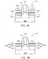
- FIG. 3Aa cross section of a strained-channel transistor structure 3 a in accordance with the first embodiment of the present invention is shown.
- Substrate 300 ahaving a strained channel region 306 a in a surface, comprises a semiconductor material.
- Gate dielectric layer 312 apreferably with a thickness between about 3 and 100 ⁇ , is on the strained channel region 306 a.
- Gate electrode 314 ais on the gate dielectric layer 312 a.
- Spacer 316 ais on a sidewall of gate electrode 314 a and covers a part of the surface of substrate 300 a.
- Drain region 307 acomprising drain extension region 301 a and deeper drain region 302 a
- source region 308 acomprising source extension region 303 a and deeper source region 304 a
- Lattice-mismatched zone 305 acomprising another semiconductor material with a natural lattice constant different from that of substrate 300 a, may be in one or both of the deeper drain region 302 a and deeper source region 304 a.
- Strained channel region 306 ais therefore strained by the different lattice constants of strained channel region 306 a and lattice-mismatched zone 305 a.
- substrate 300 apreferably comprises silicon, with a natural lattice constant of approximately 5.431 ⁇
- lattice-mismatched zone 305 apreferably comprises an alloy semiconductor material such as a silicon-germanium alloy, with a natural lattice constant between about 5.431 ⁇ to 5.657 ⁇ depending on concentration of germanium in the silicon-germanium alloy, larger than that of substrate 300 a.
- Molar fraction of germanium in the silicon-germanium alloy of lattice-mismatched zone 305 a in accordance with the first embodiment of the present inventionis preferably between about 0.1 and 0.9.
- lattice-mismatched zone 305 a as a stressorexerts a compressive stress C 1 in a source-to-drain direction and tensile stress T 1 in a vertical direction on the strained channel region 306 a, resulting in strained channel region 306 a under a compressive strain in the source-to-drain direction and tensile strain in the vertical direction.
- Hole mobility in the strained channel region 306 ais significantly enhanced, enhancing drive current when strained-channel transistor structure 3 a in accordance with the first embodiment of the present invention is a P-channel transistor structure.
- FIG. 3Ba cross section of a strained-channel transistor structure 3 b in accordance with the first embodiment of the present invention is shown.
- Substrate 300 bhaving a strained channel region 306 b in a surface, comprises a semiconductor material.
- Gate dielectric layer 312 bpreferably with a thickness between about 3 and 100 ⁇ , is on the strained channel region 306 b.
- Gate electrode 314 bis on the gate dielectric layer 312 b.
- Spacer 316 bis on a sidewall of gate electrode 314 b and covers a part of the surface of substrate 300 b.
- Drain region 307 bcomprising drain extension region 301 b and deeper drain region 302 b, and source region 308 b, comprising source extension region 303 b and deeper source region 304 b, are oppositely adjacent to strained channel region 306 b.
- Lattice-mismatched zone 305 bcomprising another semiconductor material with a natural lattice constant different from that of substrate 300 b, may be in one or both of the deeper drain region 302 b and deeper source region 304 b.
- Strained channel region 306 bis therefore strained by the difference lattice constants of strained channel region 306 b and lattice-mismatched zone 305 b.
- substrate 300 bpreferably comprises silicon and lattice-mismatched zone 305 b preferably comprises an alloy semiconductor material such as a silicon-carbon alloy, with a natural lattice constant smaller than that of substrate 300 a.
- Molar fraction of carbon in the silicon-carbon alloy of lattice-mismatched zone 305 b in accordance with the first embodiment of the present inventionis preferably between about 0.01 and 0.04.
- lattice-mismatched zone 305 bas a stressor exerts a tensile stress T 2 in a source-to-drain direction and compressive stress C 2 in a vertical direction on the strained channel region 306 b, resulting in strained channel region 306 b under a tensile strain in the source-to-drain direction and compressive strain in the vertical direction. Electron mobility in the strained channel region 306 b is significantly enhanced, enhancing drive current when strained-channel transistor structure 3 b in accordance with the first embodiment of the present invention is an N-channel transistor structure. Furthermore, lattice-mismatched zone 305 b may further comprise germanium as a silicon-germanium-carbon alloy, in which molar fraction of carbon is more than a tenth of that of germanium.
- compressive strain and tensile strain of strained channel region 306 a in FIG. 3A and strained channel region 306 b in FIG. 3Bare about 0.1% to 4%, preferably about 1% to 4%.
- Both lattice-mismatched zone 305 a in FIG. 3A and lattice-mismatched zone 305 b in FIG. 3Bare about 10 ⁇ and 1000 ⁇ thick.
- 3Bare dependent on lattice constants of lattice-mismatched zones 306 a and 306 b, thicknesses of lattice-mismatched zones 306 a and 306 b, and arrangement of lattice-mismatched zone 306 a in drain region 307 a and/or source region 308 a, and lattice-mismatched zone 306 b in drain region 307 b and/or source region 308 b.
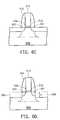
- strained-channel transistor structures 4 a through 4 d in FIGS. 4A through 4Drelationships among substrate 400 , drain extension region 401 , deeper drain region 402 , drain region 407 , source extension region 403 , deeper source region 404 , source region 408 , lattice-mismatched zone 405 a / 405 b/ 405 c/ 405 d, strained channel region 406 a / 406 b / 406 c/ 406 d, gate dielectric layer 412 , gate electrode 414 , and spacer 416 , the same as those described in the first embodiment of the present invention, are omitted.
- lattice-mismatched zone 405 ais arranged near the surface of drain region 407 and/or source region 408 , and does not extend into drain extension region 401 and/or source extension region 403 .
- lattice-mismatched zone 405 bmay protrude from the surface of drain region 407 and/or source region 408 , forming a raised drain region 407 b and raised source region 408 b.
- lattice-mismatched zone 405 cis arranged near the surface of drain region 407 and/or source region 408 , and may further extend into drain extension region 401 and/or source extension region 403 .
- FIG. 4Alattice-mismatched zone 405 a is arranged near the surface of drain region 407 and/or source region 408 , and does not extend into drain extension region 401 and/or source extension region 403 .
- lattice-mismatched zone 405 bmay protrude from the surface of drain region 407 and/or source
- lattice-mismatched zone 405 dis arranged more deeply from the surface of drain region 407 and/or source region 408 , and may further extend into strained channel region 406 d beneath drain extension region 401 and/or source extension region 403 .
- the arrangements of lattice-mismatched zone in drain region and/or source region in accordance with the first embodiment of the present inventionare not meant to be restrictive. Those skilled in the art may further adjust the arrangement of lattice-mismatched zone according to the present invention when required.
- a conductive layer 420such as silicon, metal, metal silicide, or combinations thereof is optionally formed on the surface of drain region 407 and/or source region 408 of strained-channel transistor structures 4 a, 4 c, and 4 d, and raised drain region 407 b and/or raised source region 408 b of strained-channel transistor structure 4 b.
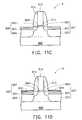
- FIG. 5A flowchart of the fabrication method in accordance with the third embodiment of the present invention is shown in FIG. 5. The subsequent descriptions of the fabrication method in accordance with the third embodiment of the present invention follow the steps in FIG. 5.
- a semiconductor substratesuch as a silicon substrate 500 is provided.
- Silicon substrate 500comprises a previously formed plurality of isolation regions (not shown) and previously defined plurality of device regions (not shown).
- the isolation regionsmay be shallow trench isolation regions.
- FIGS. 6A through 6Fprovide a cross-sectional view of one single device region for easy description.
- Silicon substrate 500comprises, a channel region 506 in an active surface.
- Silicon substrate 500is N-type doped when strained-channel transistor structure 5 in FIG. 6E is a P-channel transistor structure, or P-type doped when strained-channel transistor structure 5 in FIG. 6E is an N-channel transistor structure.
- a gate dielectric layer 512is formed on the channel region 506 , and then a gate electrode 514 is formed on the gate dielectric layer 512 .
- Gate dielectric layer 512is formed by thermal oxidation, thermal oxidation followed by nitridation, chemical vapor deposition, physical vapor deposition such as sputtering, or other known techniques to form a gate dielectric layer.
- Gate dielectric layer 512can be silicon dioxide, silicon oxynitride, or combinations thereof with a thickness between about 3 A to 100 A, preferably approximately 10 ⁇ or less.
- Gate dielectric layer 512may be a high permittivity (high-k) material such as aluminum oxide (Al 2 O 3 ), hafnium oxide (HfO 2 ), zirconium oxide (ZrO 2 ), hafnium oxynitride (HfON), hafnium silicate (HfSiO 4 ), zirconium silicate (ZrSiO 4 ), lanthanum oxide (La 2 O 3 ), or combinations thereof with an equivalent oxide thickness between about 3 ⁇ to 100 ⁇ .
- high-khigh permittivity
- Gate electrode 514is polycrystalline-silicon (poly-Si), poly-crystalline silicon-germanium (poly-SiGe), refractory metal such as molybdenum or tungsten, compounds such as titanium nitride, combinations thereof or other conductive material(s). Implants known as workfunction implants may be introduced in gate electrode 514 to alter the workfunction thereof. Gate electrode 514 is formed by depositing a gate electrode material layer (not shown) over substrate 500 , depositing a gate mask (not shown) over the gate electrode material layer, patterning the gate mask to define gate electrode 514 , etching the gate electrode material layer to form gate electrode 514 , and removing the gate mask. Gate electrode 514 is electrically isolated from channel region 506 by gate dielectric layer 512 .
- Gate dielectric layer 512is preferably silicon oxynitride and gate electrode 514 is preferably poly-silicon etched using chlorine and bromine chemistry with a high etch selectivity with respect to gate dielectric later 514 in accordance with the third embodiment of the present invention.
- a drain extension region 501 and source extension region 503are formed oppositely adjacent to channel region 506 in the active surface of substrate 500 , and spacer 516 is formed on a sidewall of gate electrode 514 , covering a part of drain extension region 501 and source extension region 503 .
- the drain extension region 501 and source extension region 503are formed by ion implantation, plasma immersion ion implantation (PIII), or other known techniques.
- Spacer 516is preferably formed by depositing a spacer material layer (not shown) such as silicon nitride or silicon dioxide, and selectively etching the spacer material layer. Spacer 516 is silicon nitride in accordance with the third embodiment of the present invention.
- a part or all of the active surface of substrate 500 not covered by gate dielectric layer 512 and spacer 516is recessed to form at least one recess 509 with a depth d by plasma etching using chlorine and bromine chemistry.
- the depth d of recess 509is about 50 ⁇ to 1000 ⁇ .
- An optional annealmay be performed to facilitate silicon migration to repair etch damage caused by etching recess 509 to smooth the surface of recess 509 for a subsequent epitaxy process.
- recess 509is filled with a semiconductor material such as silicon-germanium alloy or silicon-carbon alloy to form a lattice-mismatched zone 505 , and then a deeper drain region 502 is formed adjacent to the drain extension region 501 and a deeper source region 503 is formed adjacent to the source extension region 502 .
- Deeper drain region 502combines with drain extension region 501 to form a drain region 507
- deeper source region 504combines with source extension region 503 to form a source region 508 .
- One or both of the drain region 507 and source region 508comprise the lattice-mismatched zone 505 .
- Channel region 506is strained to be a strained channel region 506 ′ when lattice-mismatched zone 505 is formed.
- strained-channel transistor structure 5 in accordance with the third embodiment of the present inventionis basically formed.
- Lattice-mismatched zone 505is formed using an epitaxy process such as chemical vapor deposition, ultra-high vacuum chemical vapor deposition, or molecular beam epitaxy.
- Lattice-mismatched zone 505comprises silicon-germanium alloy where molar fraction of germanium is about 0.1 to 0.9 when strained-channel transistor structure 5 is a P-channel transistor structure.
- lattice-mismatched zone 505comprises silicon-carbon alloy where molar fraction of carbon is between about 0.01 and 0.04, and may further comprise germanium to be silicon-carbon-germanium alloy where molar fraction of germanium is less than ten times that of carbon.
- a silicon cap 522is optionally formed on lattice-mismatched zone 505 using an epitaxy process such as chemical vapor deposition, ultra-high vacuum chemical vapor deposition, or molecular beam epitaxy. Lattice-mismatched zone 505 and optional silicon cap 522 may be in-situ doped or undoped during the epitaxy process.
- lattice-mismatched zone 505 and optional silicon cap 522When lattice-mismatched zone 505 and optional silicon cap 522 are undoped during the epitaxy process, they will be subsequently doped, with dopants activated using a rapid thermal annealing process. Deeper drain region 502 and deeper source region 504 are formed using ion implantation, PIII, gas or solid source diffusion, or other known techniques. An annealing step is further added to recover implant damage or amorphization during formation of lattice-mismatched zone 505 , silicon cap 522 , deeper drain region 502 , and deeper source region 504 .
- a conductive layer 520is optionally formed on lattice-mismatched zone 505 and/or drain region 507 /source region 508 to reduce resistances of drain region 507 and source region 508 .
- Conductive layer 520is formed using self-aligned silicide, or other metal deposition process. Passivation layers and device contacts are subsequently formed so as to finish a device comprising strained-channel transistor structure 5 in accordance with the third embodiment of the present invention.
- FIG. 7A flowchart of the fabrication method in accordance with the third embodiment of the present invention is shown in FIG. 7. The subsequent descriptions of the fabrication method in accordance with the third embodiment of the present invention follow the steps in FIG. 7.
- FIG. 8Aa semiconductor substrate such as a silicon substrate 600 is provided.
- Silicon substrate 600comprises a previously formed plurality of isolation regions (not shown) and previously defined plurality of device regions (not shown).
- the isolation regionsmay be shallow trench isolation regions.
- FIGS. 8A through 8Dprovide a cross-sectional view of one single device region for easy description.
- Silicon substrate 600comprises a conventional transistor structure comprising a channel region 606 in an active surface of substrate 600 , a gate dielectric layer 612 on channel region 606 , a gate electrode 614 on gate dielectric layer 612 , a source region 608 and drain region 607 oppositely adjacent to channel region 606 , and a spacer 616 on a sidewall of gate electrode 614 , covering a part of the active surface of substrate 600 .
- Drain region 607comprises a drain extension region 601 and a deeper drain region 602
- source region 608comprises a source extension region 603 and a deeper source region 604 .
- Silicon substrate 600is N-type doped when strained-channel transistor structure 6 in FIG. 8C is a P-channel transistor structure, or P-type doped when strained-channel transistor structure 6 in FIG. 8C is an N-channel transistor structure.
- a part or all of the active surface of substrate 600 not covered by gate dielectric layer 612 and spacer 616is recessed to form at least one recess 609 with a depth d by plasma etching using chlorine and bromine chemistry.
- the depth d of recess 609is about 50 ⁇ to 1000 ⁇ .
- An optional annealmay be performed to facilitate silicon migration to repair etch damage caused by etching recess 606 to smooth the surface of recess 609 for a subsequent epitaxy process.
- recess 609is filled with a semiconductor material such as silicon-germanium alloy or silicon-carbon alloy to form a lattice-mismatched zone 605 .
- a semiconductor materialsuch as silicon-germanium alloy or silicon-carbon alloy to form a lattice-mismatched zone 605 .
- One or both of the drain region 607 and source region 608comprise the lattice-mismatched zone 605 .
- Channel region 606is strained to be a strained channel region 606 ′ when lattice-mismatched zone 605 is formed.
- strained-channel transistor structure 6 in accordance with the fourth embodiment of the present inventionis basically formed.
- Lattice-mismatched zone 605may protrude from the surface of drain region 607 and/or source region 608 , forming a raised drain region and raised source region.
- Lattice-mismatched zone 605is formed using an epitaxy process such as chemical vapor deposition, ultra-high vacuum chemical vapor deposition, or molecular beam epitaxy.
- Lattice-mismatched zone 605comprises silicon-germanium alloy where molar fraction of germanium is about 0.1 to 0.9 when strained-channel transistor structure 6 is a P-channel transistor structure.
- lattice-mismatched zone 605comprises silicon-carbon alloy where molar fraction of carbon is between about 0.01 and 0.04, and may further comprise germanium to be silicon-carbon-germanium alloy where molar fraction of germanium is less than ten times that of carbon.
- a silicon cap 622is optionally formed on lattice-mismatched zone 605 using an epitaxy process such as chemical vapor deposition, ultra-high vacuum chemical vapor deposition, or molecular beam epitaxy.
- Lattice-mismatched zone 605 and optional silicon cap 622are in-situ doped during the epitaxy process.
- a conductive layer 620is optionally formed on lattice-mismatched zone 605 and/or drain region 607 /source region 608 to reduce resistances of drain region 607 and source region 608 .
- Conductive layer 620is formed using self-aligned silicide, or other metal deposition process. Passivation layers and device contacts are subsequently formed so as to finish a device comprising strained-channel transistor structure 6 in accordance with the third embodiment of the present invention.
- FIG. 9A flowchart of the fabrication method in accordance with the third embodiment of the present invention is shown in FIG. 9. The subsequent descriptions of the fabrication method in accordance with the third embodiment of the present invention follow the steps in FIG. 9.
- a semiconductor substratesuch as a silicon substrate 700 is provided.
- Silicon substrate 700comprises a previously formed plurality of isolation regions (not shown) and previously defined plurality of device regions (not shown).
- the isolation regionsmay be shallow trench isolation regions.
- FIGS. 10A through 10Gprovide a cross-sectional view of one single device region for easy description.
- Silicon substrate 700comprises a channel region 706 in an active surface.
- Silicon substrate 700is N-type doped when strained-channel transistor structure 7 in FIG. 10D is a P-channel transistor structure, or P-type doped when strained-channel transistor structure 7 in FIG. 10D is an N-channel transistor structure.
- a gate dielectric layer 712is formed on the channel region 706 , and a gate electrode 714 is formed on the gate dielectric layer 712 . Finally, spacer 715 is formed on a sidewall of gate electrode 714 , covering a part of the active surface of substrate 700 .
- Gate dielectric layer 712is formed by thermal oxidation, thermal oxidation followed by nitridation, chemical vapor deposition, physical vapor deposition such as sputtering, or other known techniques to form a gate dielectric layer.
- Gate dielectric layer 712is preferably silicon dioxide, silicon oxynitride, or combinations thereof with a thickness between about 3 ⁇ to 100 ⁇ , preferably approximately 10 ⁇ or less.
- Gate dielectric layer 712may be a high permittivity (high-k) material such as aluminum oxide (Al 2 O 3 ), hafnium oxide (HfO 2 ), zirconium oxide (ZrO 2 ), hafnium oxynitride (HfON), hafnium silicate (HfSiO 4 ), zirconium silicate (ZrSiO 4 ), lanthanum oxide (La 2 O 3 ), or combinations thereof with an equivalent oxide thickness between about 3 ⁇ to 100 ⁇ .
- high-khigh permittivity
- Gate electrode 714is polycrystalline-silicon (poly-Si), poly-crystalline silicon-germanium (poly-SiGe), refractory metal such as molybdenum or tungsten, compounds such as titanium nitride, combinations thereof or other conductive material(s). Implants known as workfunction implants may be introduced in gate electrode 714 to alter the workfunction thereof. Gate electrode 714 is formed by depositing a gate electrode material layer (not shown) over substrate 700 , depositing a gate mask (not shown) over the gate electrode material layer, patterning the gate mask to define gate electrode 714 , etching the gate electrode material layer to form gate electrode 714 , and removing the gate mask. Gate electrode 714 is electrically isolated from channel region 706 by gate dielectric layer 712 .
- Gate dielectric layer 712is preferably silicon oxynitride and gate electrode 714 is poly-silicon etched using chlorine and bromine chemistry with a high etch selectivity with respect to gate dielectric later 714 in accordance with the third embodiment of the present invention.
- Spacer 715is formed using a deposition and anisotropic etching technique for protecting the sidewall of gate electrode 714 during a subsequent epitaxy step.
- a part or all of the active surface of substrate 700 not covered by gate dielectric layer 712 and spacer 715is recessed to form at least one recess 709 with a depth d by plasma etching using chlorine and bromine chemistry.
- the depth d of recess 709is about 50 ⁇ to 1000 ⁇ .
- An optional annealmay be performed to facilitate silicon migration to repair etch damage caused by etching recess 706 to smooth the surface of recess 709 for a subsequent epitaxy process.
- strained-channel transistor structure 7in accordance with the fifth embodiment of the present invention is basically formed.
- Lattice-mismatched zone 705is formed using an epitaxy process such as chemical vapor deposition, ultra-high vacuum chemical vapor deposition, or molecular beam epitaxy.
- Channel region 706is strained to be a strained channel region 706 ′ when lattice-mismatched zone 705 is formed.
- Lattice-mismatched zone 705comprises silicon-germanium alloy where molar fraction of germanium is about 0.1 to 0.9 when strained-channel transistor structure 7 is a P-channel transistor structure.
- lattice-mismatched zone 705comprises silicon-carbon alloy where molar fraction of carbon is between about 0.01 and 0.04, and may further comprise germanium to be silicon-carbon-germanium alloy where molar fraction of germanium is less than ten times that of carbon.
- a silicon cap 722is optionally formed on-lattice-mismatched zone 705 using an epitaxy process such as chemical vapor deposition, ultra-high vacuum chemical vapor deposition, or molecular beam epitaxy.
- Lattice-mismatched zone 705 and optional silicon cap 722may be in-situ doped or undoped during the epitaxy process. When lattice-mismatched zone 705 and optional silicon cap 722 are undoped during the epitaxy process, but will be doped subsequently, at which time dopants will be activated using a rapid thermal annealing process. Drain extension region 701 and source extension region 703 are formed by dopant diffusion from lattice-mismatched zone 705 and optional silicon cap 722 . One or both of the drain extension region 701 and source extension region 703 comprise the lattice-mismatched zone 705 and optional silicon cap 722 .
- a spacer 716is formed overlying the spacer 715 .
- Spacer 716is formed using deposition and selectively etching a spacer material (not shown) such as silicon nitride or silicon dioxide.
- Spacer 716is silicon nitride in accordance with the third embodiment of the present invention.
- a deeper drain region 702is formed adjacent to drain extension region 701
- deeper source region 704is formed adjacent to source extension region 702 .
- Deeper drain region 702combines with drain extension region 701 , lattice-mismatched zone 705 when available, and optional silicon cap 722 when available to be a drain region 707
- deeper source region 704combines with source extension region 703 , lattice-mismatched zone 705 when available, and optional silicon cap 722 when available to be a source region 708 .
- Deeper drain region 702 and deeper source region 704are formed using ion implantation, PIII, gas or solid source diffusion, or other known techniques.
- a conductive layer 720is optionally formed on drain region 707 and source region 708 to reduce resistances of drain region 707 and source region 708 .
- Conductive layer 720is formed using self-aligned silicide, or other metal deposition. Passivation layers and device contacts are subsequently formed so as to finish a device comprising strained-channel transistor structure 7 in accordance with the fifth embodiment of the present invention.
- FIG. 11Aa semiconductor substrate such as a silicon substrate 800 is provided.
- Silicon substrate 800comprises a previously formed plurality of isolation regions (not shown) and previously defined plurality of device regions (not shown).
- the isolation regionsmay be shallow trench isolation regions.
- FIGS. 11A through 11Dprovide a cross-sectional view of one single device region for easy description.
- Silicon substrate 800comprises a conventional transistor structure comprising a channel region 806 in an active surface of substrate 800 , a gate dielectric layer 812 on channel region 806 , a gate electrode 814 on gate dielectric layer 812 , a source region 808 and drain region 807 oppositely adjacent to channel region 806 , and a spacer 816 on a sidewall of gate electrode 814 , covering a part of the active surface of substrate 800 .
- Drain region 807comprises a drain extension region 801 and a deeper drain region 802
- source region 808comprises a source extension region 803 and a deeper source region 804 .
- Silicon substrate 800is N-type doped when strained-channel transistor structure 8 in FIG. 11C is a P-channel transistor structure, or P-type doped when strained-channel transistor structure 8 in FIG. 11C is an N-channel transistor structure.
- an ion implantation processis performed to introduce ions 830 of one or more atomic species with a different atomic size from that of substrate 800 into drain region 807 and/or source region 808 .
- Gate electrode 814 and spacer 816act as a implantation mask during the ion implantation process. Thickness of spacer 816 is adjustable depending on lattice-mismatched zone 805 in FIG. 11C either extending into drain extension region 801 and/or source extension region 803 , or not extending into drain extension region 801 and/or source extension region 803 , as required.
- an annealing stepis performed on the substrate 800 to form a lattice-mismatched zone in one or both of drain region 807 and source region 808 .
- the drain region 807 and source region 808comprise the lattice-mismatched zone 805 .
- Channel region 806is strained to be a strained channel region 806 ′ when lattice-mismatched zone 805 is formed.
- strained-channel transistor structure 8 in accordance with the sixth embodiment of the present inventionis basically formed.
- Lattice-mismatched zone 805comprises silicon-germanium alloy where molar fraction of germanium is about 0.1 to 0.9 when strained-channel transistor structure 8 is a P-channel transistor structure.
- lattice-mismatched zone 805comprises silicon-carbon alloy where molar fraction of carbon is between about 0.01 and 0.04, and may further comprise germanium to be silicon-carbon-germanium alloy where molar fraction of germanium is less than ten times that of carbon.
- a conductive layer 820is optionally formed on drain region 807 and source region 808 to reduce resistances of drain region 807 and source region 808 .
- Conductive layer 820is formed using self-aligned silicide, or other metal deposition process. Passivation layers and device contacts are subsequently formed so as to finish a device comprising strained-channel transistor structure 8 in accordance with the sixth embodiment of the present invention.
Landscapes
- Engineering & Computer Science (AREA)
- Condensed Matter Physics & Semiconductors (AREA)
- Crystallography & Structural Chemistry (AREA)
- General Chemical & Material Sciences (AREA)
- Physics & Mathematics (AREA)
- Chemical Kinetics & Catalysis (AREA)
- Chemical & Material Sciences (AREA)
- General Physics & Mathematics (AREA)
- Manufacturing & Machinery (AREA)
- Computer Hardware Design (AREA)
- Microelectronics & Electronic Packaging (AREA)
- Power Engineering (AREA)
- Insulated Gate Type Field-Effect Transistor (AREA)
Abstract
Description
- 1. Field of the Invention[0001]
- The present invention relates to a semiconductor device with lattice-mismatched zone and fabrication method thereof, and more specifically to a strained-channel transistor structure and fabrication method thereof.[0002]
- 2. Description of the Related Art[0003]
- Size reduction of the metal-oxide-semiconductor field-effect transistor (MOSFET), including reduction of gate length and gate oxide thickness, has enabled a continuous improvement in speed performance, density, and cost per unit function of integrated circuits during the past few decades.[0004]
- In order to further enhance performance of the transistor, strain may be introduced in the transistor channel to improve carrier mobility to enhance performance of the transistor in addition to device scaling. There are several existing approaches to introducing strain in a channel region of the transistor.[0005]
- In one conventional approach, as described in a paper titled “NMOS and PMOS transistors fabricated in strained silicon/relaxed silicon-germanium structures”, disclosed by J. Welser et al., published at the December 1992 International Electron Devices Meeting held in San Francisco, Calif., pp. 1000-1002, a relaxed silicon germanium (SiGe)[0006]
buffer layer 110 is provided beneathchannel region 126, as shown in FIG. 1A. In FIG. 1B and FIG. 1C, a simple model of different lattice constants is used to show the intersection betweenrelaxed SiGe layer 114 ofbuffer layer 110 and strained-Si layer130. In FIG. 1B,model 135 shows the natural lattice constant of Si, smaller than that of SiGe shown bymodel 115. In FIG. 1C, when a thin layer of epitaxial Si (model135) is grown on relaxed SiGe layer114 (model115),unit cell 136 of Si shown inmodel 135 is stretched laterally so as to be under a biaxial tensile strain. The thin layer of epitaxial Si becomes strain-Si layer130 shown in FIG. 1A. In FIG. 1A, a transistor formed on the epitaxial strained-Si layer130 is therefore with achannel region 126 under the biaxial tensile strain. In this approach,relaxed SiGe layer 114 is a stressor that introduces strain inchannel region 126. The stressor, in this case, is placed belowchannel region 126. Significant mobility enhancement has been reported for both electrons and holes in bulk transistors using a silicon channel under biaxial tensile strain. In the aforementioned approach, the epitaxial silicon layer130 is strained before forming the transistor. Therefore, there are some concerns about possible strain relaxation in the subsequent high temperature CMOS processes. Further, the approach is very expensive since SiGebuffer layer 110 with thickness in the order of micrometers has to be grown. Numerous dislocations exist inrelaxed SiGe layer 114, some of which propagate to strained-Si layer130, resulting in high defect density, thereby negatively affecting transistor performance. - In another approach, strain in a channel region is introduced after a transistor is formed. In this approach, a[0007]
high stress film 220 is formed over a completedtransistor structure 250, as shown in FIG. 2.High stress film 220, being a stressor, exerts significant influence onchannel region 206, modifying silicon lattice spacing inchannel region 206, and thus introducing strain inchannel region 206. In this case, the stressor is placed above completedtransistor structure 250, described in detail in a paper disclosed by A. Shimizu et al., entitled “Local mechanical stress control (LMC): a new technique for CMOS performance enhancement”, published in pp. 433-436 of theDigest of Technical Papersof the 2001International Electron Device Meeting.The strain contributed byhigh stress film 220 is believed to be uniaxial in nature with a direction parallel to a source-to-drain direction. However, uniaxial tensile strain in the source-to-drain degrades hole mobility while uniaxial compressive strain degrades electron mobility. Ion implantation of germanium can be used to selectively relax the strain so that the hole or electron mobility is not degraded, but can be difficult to implement due to the close proximity of the N and P-channel transistors. - Thus, the main object of the present invention is to provide a transistor structure with a strained channel region.[0008]
- Another object of the present invention is to provide a strained-channel transistor structure where portions of one or both of a source region and drain region adjacent to a strained channel region are lattice mismatched with respect to the channel region.[0009]
- Another object of the present invention is to provide a fabrication method of a strained-channel transistor structure.[0010]
- In order to achieve the above objects, the present invention provides a strained-channel transistor structure comprising a strained channel region, a gate dielectric layer, a gate electrode, and a source region and drain region. The substrate comprises a first semiconductor material with a first natural lattice constant. The gate dielectric layer is on the strained channel region. The gate electrode is on the gate dielectric layer. The source region and drain region are oppositely adjacent to the strained channel region. One or both of the source region and drain region comprise a lattice-mismatched zone comprising a second semiconductor material with a second natural lattice constant different from the first natural lattice constant.[0011]
- The present invention further provides a fabrication method of a strained-channel transistor structure. First, a substrate having a channel region, comprising a first semiconductor material with a first natural lattice constant, in a surface, a gate dielectric on the channel region, and a gate electrode on the gate dielectric layer is provided. Then, a first source region and drain region are formed oppositely adjacent to the channel region. Next, a spacer is formed on a sidewall of the gate electrode, covering a part of the surface of the substrate. Next, the surface of the substrate not covered by the spacer and gate electrode is recessed. Further, the recess is filled with a second semiconductor material with a second natural lattice constant different from the first natural lattice constant as a lattice-mismatched zone straining the channel region. Finally, a second source region is formed adjacent to the first source region and a second drain region is formed adjacent to the first drain region, one or both of the second source region and second drain region comprising the lattice-mismatched zone.[0012]
- The present invention further provides a fabrication method of a strained-channel transistor structure. First, a substrate having a channel region, comprising a first semiconductor material with a first natural lattice constant, in a surface, a gate dielectric on the channel region, a gate electrode on the gate dielectric layer, a source region and drain region oppositely adjacent to the channel region, and a spacer on a sidewall of the gate electrode, covering a part of the surface of the substrate, is provided. Then, one or both of the source region and drain region is recessed. Finally, the recess is filled with a second semiconductor material with a second natural lattice constant different from the first natural lattice constant as a lattice-mismatched zone straining the channel region.[0013]
- The present invention further provides a fabrication method of a strained-channel transistor structure. First, a substrate having a channel region, comprising a first semiconductor material with a first natural lattice constant, in a surface, a gate dielectric on the channel region, a gate electrode on the gate dielectric layer, and a spacer on a sidewall of the gate electrode, covering a part of the surface of the substrate, is provided. Then, the surface of the substrate not covered by the spacer and gate dielectric layer is recessed to form a recess. Finally, a source region and drain region are formed oppositely adjacent to the channel region, one or both of the source region and drain region comprising the lattice-mismatched zone.[0014]
- The present invention further provides a fabrication method of a strained-channel transistor structure. First, a substrate having a channel region, comprising a semiconductor material, in a surface, a gate dielectric on the channel region, a gate electrode on the gate dielectric layer, a source region and drain region oppositely adjacent to the channel region, and a spacer on a sidewall of the gate electrode, covering a part of the surface of the substrate, is provided. Finally, an element with an atomic size different from that of the semiconductor material is implanted to form a lattice-mismatched zone in one or both of the source region and drain region straining the channel region.[0015]
- The present invention can be more fully understood by reading the subsequent detailed description in conjunction with the examples with references made to the accompanying drawings, wherein:[0016]
- FIGS. 1A through 1C are cross sections illustrating a conventional strained silicon transistor with a relaxed SiGe layer as a stressor to induce strain in the top epitaxial strained silicon layer.[0017]
- FIG. 2 is a cross section illustrating another conventional strained silicon transistor introducing strain in the channel using a high stress film as a stressor.[0018]
- FIG. 3A and FIG. 3B are cross sections illustrating strained-channel transistor structures in accordance with the first embodiment of the present invention.[0019]
- FIGS. 4A through 4B are cross sections illustrating strained-channel transistor structures in accordance with the second embodiment of the present invention.[0020]
- FIG. 5 is a flowchart illustrating, in detail, the fabrication method of a strained-channel transistor structure in accordance with the third embodiment of the present invention.[0021]
- FIGS. 6A through 6F are cross sections illustrating steps of the fabrication method of a strained-channel transistor structure in accordance with the third embodiment of the present invention.[0022]
- FIG. 7 is a flowchart illustrating, in detail, the fabrication method of a strained-channel transistor structure in accordance with the fourth embodiment of the present invention.[0023]
- FIGS. 8A through 8D are cross sections illustrating steps of the fabrication method of a strained-channel transistor structure in accordance with the fourth embodiment of the present invention.[0024]
- FIG. 9 is a flowchart illustrating, in detail, the fabrication method of a strained-channel transistor structure in accordance with the fifth embodiment of the present invention.[0025]
- FIGS. 10A through 10G are cross sections illustrating steps of the fabrication method of a strained-channel transistor structure in accordance with the fifth embodiment of the present invention.[0026]
- FIGS. 11A through 11D are cross sections illustrating steps of the fabrication method of a strained-channel transistor structure in accordance with the sixth embodiment of the present invention.[0027]
- The following embodiments are intended to illustrate the invention more fully without limiting their scope, since numerous modifications and variations will be apparent to those skilled in this art.[0028]
- In the first embodiment of the present invention, two kinds of stress modes exerted on the strained-channel region according to the present invention are discussed.[0029]
- In FIG. 3A, a cross section of a strained-[0030]
channel transistor structure 3ain accordance with the first embodiment of the present invention is shown.Substrate 300a,having astrained channel region 306ain a surface, comprises a semiconductor material.Gate dielectric layer 312a,preferably with a thickness between about 3 and 100 Å, is on thestrained channel region 306a.Gate electrode 314ais on thegate dielectric layer 312a.Spacer 316ais on a sidewall ofgate electrode 314aand covers a part of the surface ofsubstrate 300a.Drain region 307a,comprisingdrain extension region 301aanddeeper drain region 302a,andsource region 308a,comprisingsource extension region 303aanddeeper source region 304a,are oppositely adjacent tostrained channel region 306a.Lattice-mismatchedzone 305a,comprising another semiconductor material with a natural lattice constant different from that ofsubstrate 300a,may be in one or both of thedeeper drain region 302aanddeeper source region 304a.Strained channel region 306ais therefore strained by the different lattice constants ofstrained channel region 306aand lattice-mismatchedzone 305a. - In strained-[0031]
channel transistor structure 3ain accordance with the first embodiment of the present invention,substrate 300apreferably comprises silicon, with a natural lattice constant of approximately 5.431 Å, and lattice-mismatchedzone 305apreferably comprises an alloy semiconductor material such as a silicon-germanium alloy, with a natural lattice constant between about 5.431 Å to 5.657 Å depending on concentration of germanium in the silicon-germanium alloy, larger than that ofsubstrate 300a.Molar fraction of germanium in the silicon-germanium alloy of lattice-mismatchedzone 305ain accordance with the first embodiment of the present invention is preferably between about 0.1 and 0.9. Therefore, lattice-mismatchedzone 305aas a stressor exerts a compressive stress C1in a source-to-drain direction and tensile stress T1in a vertical direction on thestrained channel region 306a,resulting instrained channel region 306aunder a compressive strain in the source-to-drain direction and tensile strain in the vertical direction. Hole mobility in thestrained channel region 306ais significantly enhanced, enhancing drive current when strained-channel transistor structure 3ain accordance with the first embodiment of the present invention is a P-channel transistor structure. - In FIG. 3B, a cross section of a strained-[0032]
channel transistor structure 3bin accordance with the first embodiment of the present invention is shown.Substrate 300b,having astrained channel region 306bin a surface, comprises a semiconductor material.Gate dielectric layer 312b,preferably with a thickness between about 3 and 100 Å, is on thestrained channel region 306b.Gate electrode 314bis on thegate dielectric layer 312b.Spacer 316bis on a sidewall ofgate electrode 314band covers a part of the surface ofsubstrate 300b.Drain region 307b,comprising drain extension region301banddeeper drain region 302b,andsource region 308b,comprisingsource extension region 303banddeeper source region 304b,are oppositely adjacent tostrained channel region 306b.Lattice-mismatchedzone 305b,comprising another semiconductor material with a natural lattice constant different from that ofsubstrate 300b,may be in one or both of thedeeper drain region 302banddeeper source region 304b.Strained channel region 306bis therefore strained by the difference lattice constants ofstrained channel region 306band lattice-mismatchedzone 305b. - In strained-[0033]
channel transistor structure 3bin accordance with the first embodiment of the present invention,substrate 300bpreferably comprises silicon and lattice-mismatchedzone 305bpreferably comprises an alloy semiconductor material such as a silicon-carbon alloy, with a natural lattice constant smaller than that ofsubstrate 300a.Molar fraction of carbon in the silicon-carbon alloy of lattice-mismatchedzone 305bin accordance with the first embodiment of the present invention is preferably between about 0.01 and 0.04. Therefore, lattice-mismatchedzone 305bas a stressor exerts a tensile stress T2in a source-to-drain direction and compressive stress C2in a vertical direction on thestrained channel region 306b,resulting instrained channel region 306bunder a tensile strain in the source-to-drain direction and compressive strain in the vertical direction. Electron mobility in thestrained channel region 306bis significantly enhanced, enhancing drive current when strained-channel transistor structure 3bin accordance with the first embodiment of the present invention is an N-channel transistor structure. Furthermore, lattice-mismatchedzone 305bmay further comprise germanium as a silicon-germanium-carbon alloy, in which molar fraction of carbon is more than a tenth of that of germanium. - Further, compressive strain and tensile strain of[0034]
strained channel region 306ain FIG. 3A andstrained channel region 306bin FIG. 3B are about 0.1% to 4%, preferably about 1% to 4%. Both lattice-mismatchedzone 305ain FIG. 3A and lattice-mismatchedzone 305bin FIG. 3B are about 10 Å and 1000 Å thick. Compressive strain and tensile strain ofstrained channel region 306ain FIG. 3A andstrained channel region 306bin FIG. 3B are dependent on lattice constants of lattice-mismatchedzones zones zone 306aindrain region 307aand/orsource region 308a,and lattice-mismatchedzone 306bindrain region 307band/orsource region 308b. - In the second embodiment of the present invention, different kinds of arrangements of lattice-mismatched zone in drain region and/or source region according to the present invention are discussed. In strained-[0035]
channel transistor structures 4athrough4d in FIGS. 4A through 4D, relationships amongsubstrate 400,drain extension region 401,deeper drain region 402,drain region 407,source extension region 403,deeper source region 404,source region 408, lattice-mismatchedzone 405a/405b/405c/405d,strained channel region 406a/406b/406c/406d,gate dielectric layer 412,gate electrode 414, andspacer 416, the same as those described in the first embodiment of the present invention, are omitted. - In FIG. 4A, lattice-mismatched[0036]
zone 405ais arranged near the surface ofdrain region 407 and/orsource region 408, and does not extend intodrain extension region 401 and/orsource extension region 403. In FIG. 4B, lattice-mismatchedzone 405bmay protrude from the surface ofdrain region 407 and/orsource region 408, forming a raiseddrain region 407band raisedsource region 408b.In FIG. 4C, lattice-mismatchedzone 405cis arranged near the surface ofdrain region 407 and/orsource region 408, and may further extend intodrain extension region 401 and/orsource extension region 403. In FIG. 4D, lattice-mismatchedzone 405dis arranged more deeply from the surface ofdrain region 407 and/orsource region 408, and may further extend intostrained channel region 406dbeneathdrain extension region 401 and/orsource extension region 403. Note that the arrangements of lattice-mismatched zone in drain region and/or source region in accordance with the first embodiment of the present invention are not meant to be restrictive. Those skilled in the art may further adjust the arrangement of lattice-mismatched zone according to the present invention when required. - In FIGS. 4A through 4D, a[0037]
conductive layer 420 such as silicon, metal, metal silicide, or combinations thereof is optionally formed on the surface ofdrain region 407 and/orsource region 408 of strained-channel transistor structures drain region 407band/or raisedsource region 408bof strained-channel transistor structure 4b. - Moreover, enhancement of either electron or hole mobility in strained-[0038]
channel structure 4cin FIG. 4C is further improved because lattice-mismatchedzone 405cis closer tostrained channel region 406c,resulting in lattice-mismatchedzone 405cexerting more strain onstrained channel region 406c. - In the third embodiment of the present invention, a fabrication method of a strained-channel transistor structure according to the present invention is described. A flowchart of the fabrication method in accordance with the third embodiment of the present invention is shown in FIG. 5. The subsequent descriptions of the fabrication method in accordance with the third embodiment of the present invention follow the steps in FIG. 5.[0039]
- In FIG. 6A, a semiconductor substrate such as a[0040]
silicon substrate 500 is provided.Silicon substrate 500 comprises a previously formed plurality of isolation regions (not shown) and previously defined plurality of device regions (not shown). For example, the isolation regions may be shallow trench isolation regions. FIGS. 6A through 6F provide a cross-sectional view of one single device region for easy description.Silicon substrate 500 comprises, achannel region 506 in an active surface.Silicon substrate 500 is N-type doped when strained-channel transistor structure 5 in FIG. 6E is a P-channel transistor structure, or P-type doped when strained-channel transistor structure 5 in FIG. 6E is an N-channel transistor structure. - In FIG. 6B, a[0041]
gate dielectric layer 512 is formed on thechannel region 506, and then agate electrode 514 is formed on thegate dielectric layer 512.Gate dielectric layer 512 is formed by thermal oxidation, thermal oxidation followed by nitridation, chemical vapor deposition, physical vapor deposition such as sputtering, or other known techniques to form a gate dielectric layer.Gate dielectric layer 512 can be silicon dioxide, silicon oxynitride, or combinations thereof with a thickness between about3 A to100 A, preferably approximately 10 Å or less.Gate dielectric layer 512 may be a high permittivity (high-k) material such as aluminum oxide (Al2O3), hafnium oxide (HfO2), zirconium oxide (ZrO2), hafnium oxynitride (HfON), hafnium silicate (HfSiO4), zirconium silicate (ZrSiO4), lanthanum oxide (La2O3), or combinations thereof with an equivalent oxide thickness between about 3 Å to 100 Å.Gate electrode 514 is polycrystalline-silicon (poly-Si), poly-crystalline silicon-germanium (poly-SiGe), refractory metal such as molybdenum or tungsten, compounds such as titanium nitride, combinations thereof or other conductive material(s). Implants known as workfunction implants may be introduced ingate electrode 514 to alter the workfunction thereof.Gate electrode 514 is formed by depositing a gate electrode material layer (not shown) oversubstrate 500, depositing a gate mask (not shown) over the gate electrode material layer, patterning the gate mask to definegate electrode 514, etching the gate electrode material layer to formgate electrode 514, and removing the gate mask.Gate electrode 514 is electrically isolated fromchannel region 506 bygate dielectric layer 512.Gate dielectric layer 512 is preferably silicon oxynitride andgate electrode 514 is preferably poly-silicon etched using chlorine and bromine chemistry with a high etch selectivity with respect to gate dielectric later514 in accordance with the third embodiment of the present invention. - In FIG. 6C, a[0042]
drain extension region 501 andsource extension region 503 are formed oppositely adjacent to channelregion 506 in the active surface ofsubstrate 500, andspacer 516 is formed on a sidewall ofgate electrode 514, covering a part ofdrain extension region 501 andsource extension region 503. Thedrain extension region 501 andsource extension region 503 are formed by ion implantation, plasma immersion ion implantation (PIII), or other known techniques.Spacer 516 is preferably formed by depositing a spacer material layer (not shown) such as silicon nitride or silicon dioxide, and selectively etching the spacer material layer.Spacer 516 is silicon nitride in accordance with the third embodiment of the present invention. - In FIG. 6D, a part or all of the active surface of[0043]
substrate 500 not covered bygate dielectric layer 512 andspacer 516 is recessed to form at least onerecess 509 with a depth d by plasma etching using chlorine and bromine chemistry. The depth d ofrecess 509 is about 50 Å to 1000 Å. An optional anneal may be performed to facilitate silicon migration to repair etch damage caused by etchingrecess 509 to smooth the surface ofrecess 509 for a subsequent epitaxy process. - In FIG. 6E,[0044]
recess 509 is filled with a semiconductor material such as silicon-germanium alloy or silicon-carbon alloy to form a lattice-mismatchedzone 505, and then adeeper drain region 502 is formed adjacent to thedrain extension region 501 and adeeper source region 503 is formed adjacent to thesource extension region 502.Deeper drain region 502 combines withdrain extension region 501 to form adrain region 507, anddeeper source region 504 combines withsource extension region 503 to form asource region 508. One or both of thedrain region 507 andsource region 508 comprise the lattice-mismatchedzone 505.Channel region 506 is strained to be astrained channel region 506′ when lattice-mismatchedzone 505 is formed. Thus, strained-channel transistor structure 5 in accordance with the third embodiment of the present invention is basically formed. Lattice-mismatchedzone 505 is formed using an epitaxy process such as chemical vapor deposition, ultra-high vacuum chemical vapor deposition, or molecular beam epitaxy. Lattice-mismatchedzone 505 comprises silicon-germanium alloy where molar fraction of germanium is about 0.1 to 0.9 when strained-channel transistor structure 5 is a P-channel transistor structure. When strained-channel transistor structure 5 is an N-channel transistor structure, lattice-mismatchedzone 505 comprises silicon-carbon alloy where molar fraction of carbon is between about 0.01 and 0.04, and may further comprise germanium to be silicon-carbon-germanium alloy where molar fraction of germanium is less than ten times that of carbon. Asilicon cap 522 is optionally formed on lattice-mismatchedzone 505 using an epitaxy process such as chemical vapor deposition, ultra-high vacuum chemical vapor deposition, or molecular beam epitaxy. Lattice-mismatchedzone 505 andoptional silicon cap 522 may be in-situ doped or undoped during the epitaxy process. When lattice-mismatchedzone 505 andoptional silicon cap 522 are undoped during the epitaxy process, they will be subsequently doped, with dopants activated using a rapid thermal annealing process.Deeper drain region 502 anddeeper source region 504 are formed using ion implantation, PIII, gas or solid source diffusion, or other known techniques. An annealing step is further added to recover implant damage or amorphization during formation of lattice-mismatchedzone 505,silicon cap 522,deeper drain region 502, anddeeper source region 504. - In FIG. 6F, a[0045]
conductive layer 520 is optionally formed on lattice-mismatchedzone 505 and/or drainregion 507/source region 508 to reduce resistances ofdrain region 507 andsource region 508.Conductive layer 520 is formed using self-aligned silicide, or other metal deposition process. Passivation layers and device contacts are subsequently formed so as to finish a device comprising strained-channel transistor structure 5 in accordance with the third embodiment of the present invention. - In the fourth embodiment of the present invention, a fabrication method of a strained-channel transistor structure where lattice-mismatched zone does not extend into drain extension region and/or source extension region according to the present invention is described. A flowchart of the fabrication method in accordance with the third embodiment of the present invention is shown in FIG. 7. The subsequent descriptions of the fabrication method in accordance with the third embodiment of the present invention follow the steps in FIG. 7.[0046]
- In FIG. 8A, a semiconductor substrate such as a[0047]
silicon substrate 600 is provided.Silicon substrate 600 comprises a previously formed plurality of isolation regions (not shown) and previously defined plurality of device regions (not shown). For example, the isolation regions may be shallow trench isolation regions. FIGS. 8A through 8D provide a cross-sectional view of one single device region for easy description.Silicon substrate 600 comprises a conventional transistor structure comprising achannel region 606 in an active surface ofsubstrate 600, agate dielectric layer 612 onchannel region 606, agate electrode 614 ongate dielectric layer 612, asource region 608 and drainregion 607 oppositely adjacent to channelregion 606, and a spacer616 on a sidewall ofgate electrode 614, covering a part of the active surface ofsubstrate 600.Drain region 607 comprises adrain extension region 601 and adeeper drain region 602, andsource region 608 comprises asource extension region 603 and adeeper source region 604.Silicon substrate 600 is N-type doped when strained-channel transistor structure 6 in FIG. 8C is a P-channel transistor structure, or P-type doped when strained-channel transistor structure 6 in FIG. 8C is an N-channel transistor structure. - In FIG. 8B, a part or all of the active surface of[0048]
substrate 600 not covered bygate dielectric layer 612 and spacer616 is recessed to form at least onerecess 609 with a depth d by plasma etching using chlorine and bromine chemistry. The depth d ofrecess 609 is about 50 Å to 1000 Å. An optional anneal may be performed to facilitate silicon migration to repair etch damage caused by etchingrecess 606 to smooth the surface ofrecess 609 for a subsequent epitaxy process. - In FIG. 8C,[0049]
recess 609 is filled with a semiconductor material such as silicon-germanium alloy or silicon-carbon alloy to form a lattice-mismatchedzone 605. One or both of thedrain region 607 andsource region 608 comprise the lattice-mismatchedzone 605.Channel region 606 is strained to be astrained channel region 606′ when lattice-mismatchedzone 605 is formed. Thus, strained-channel transistor structure 6 in accordance with the fourth embodiment of the present invention is basically formed. Lattice-mismatchedzone 605 may protrude from the surface ofdrain region 607 and/orsource region 608, forming a raised drain region and raised source region. Lattice-mismatchedzone 605 is formed using an epitaxy process such as chemical vapor deposition, ultra-high vacuum chemical vapor deposition, or molecular beam epitaxy. Lattice-mismatchedzone 605 comprises silicon-germanium alloy where molar fraction of germanium is about 0.1 to 0.9 when strained-channel transistor structure 6 is a P-channel transistor structure. When strained-channel transistor structure 6 is an N-channel transistor structure, lattice-mismatchedzone 605 comprises silicon-carbon alloy where molar fraction of carbon is between about 0.01 and 0.04, and may further comprise germanium to be silicon-carbon-germanium alloy where molar fraction of germanium is less than ten times that of carbon. Asilicon cap 622 is optionally formed on lattice-mismatchedzone 605 using an epitaxy process such as chemical vapor deposition, ultra-high vacuum chemical vapor deposition, or molecular beam epitaxy. Lattice-mismatchedzone 605 andoptional silicon cap 622 are in-situ doped during the epitaxy process. - In FIG. 8D, a[0050]
conductive layer 620 is optionally formed on lattice-mismatchedzone 605 and/or drainregion 607/source region 608 to reduce resistances ofdrain region 607 andsource region 608.Conductive layer 620 is formed using self-aligned silicide, or other metal deposition process. Passivation layers and device contacts are subsequently formed so as to finish a device comprising strained-channel transistor structure 6 in accordance with the third embodiment of the present invention. - In the fifth embodiment of the present invention, a fabrication method of a strained-channel transistor structure where lattice-mismatched zone extends into drain extension region and/or source extension region according to the present invention is described. A flowchart of the fabrication method in accordance with the third embodiment of the present invention is shown in FIG. 9. The subsequent descriptions of the fabrication method in accordance with the third embodiment of the present invention follow the steps in FIG. 9.[0051]
- In FIG. 10A, a semiconductor substrate such as a[0052]
silicon substrate 700 is provided.Silicon substrate 700 comprises a previously formed plurality of isolation regions (not shown) and previously defined plurality of device regions (not shown). For example, the isolation regions may be shallow trench isolation regions. FIGS. 10A through 10G provide a cross-sectional view of one single device region for easy description.Silicon substrate 700 comprises achannel region 706 in an active surface.Silicon substrate 700 is N-type doped when strained-channel transistor structure 7 in FIG. 10D is a P-channel transistor structure, or P-type doped when strained-channel transistor structure 7 in FIG. 10D is an N-channel transistor structure. - In FIG. 10B, first, a[0053]
gate dielectric layer 712 is formed on thechannel region 706, and agate electrode 714 is formed on thegate dielectric layer 712. Finally,spacer 715 is formed on a sidewall ofgate electrode 714, covering a part of the active surface ofsubstrate 700.Gate dielectric layer 712 is formed by thermal oxidation, thermal oxidation followed by nitridation, chemical vapor deposition, physical vapor deposition such as sputtering, or other known techniques to form a gate dielectric layer.Gate dielectric layer 712 is preferably silicon dioxide, silicon oxynitride, or combinations thereof with a thickness between about 3 Å to 100 Å, preferably approximately 10 Å or less.Gate dielectric layer 712 may be a high permittivity (high-k) material such as aluminum oxide (Al2O3), hafnium oxide (HfO2), zirconium oxide (ZrO2), hafnium oxynitride (HfON), hafnium silicate (HfSiO4), zirconium silicate (ZrSiO4), lanthanum oxide (La2O3), or combinations thereof with an equivalent oxide thickness between about 3 Å to 100 Å.Gate electrode 714 is polycrystalline-silicon (poly-Si), poly-crystalline silicon-germanium (poly-SiGe), refractory metal such as molybdenum or tungsten, compounds such as titanium nitride, combinations thereof or other conductive material(s). Implants known as workfunction implants may be introduced ingate electrode 714 to alter the workfunction thereof.Gate electrode 714 is formed by depositing a gate electrode material layer (not shown) oversubstrate 700, depositing a gate mask (not shown) over the gate electrode material layer, patterning the gate mask to definegate electrode 714, etching the gate electrode material layer to formgate electrode 714, and removing the gate mask.Gate electrode 714 is electrically isolated fromchannel region 706 bygate dielectric layer 712.Gate dielectric layer 712 is preferably silicon oxynitride andgate electrode 714 is poly-silicon etched using chlorine and bromine chemistry with a high etch selectivity with respect to gate dielectric later714 in accordance with the third embodiment of the present invention.Spacer 715 is formed using a deposition and anisotropic etching technique for protecting the sidewall ofgate electrode 714 during a subsequent epitaxy step. - In FIG. 10C, a part or all of the active surface of[0054]
substrate 700 not covered bygate dielectric layer 712 andspacer 715 is recessed to form at least onerecess 709 with a depth d by plasma etching using chlorine and bromine chemistry. The depth d ofrecess 709 is about 50 Å to 1000 Å. An optional anneal may be performed to facilitate silicon migration to repair etch damage caused by etchingrecess 706 to smooth the surface ofrecess 709 for a subsequent epitaxy process. - In FIG. 10D,[0055]
recess 709 is filled with a semiconductor material such as silicon-germanium alloy or silicon-carbon alloy to form a lattice-mismatchedzone 505, and then adrain extension region 701 andsource extension region 702 are formed oppositely adjacent to thestrained channel region 706′. Thus, strained-channel transistor structure 7 in accordance with the fifth embodiment of the present invention is basically formed. Lattice-mismatchedzone 705 is formed using an epitaxy process such as chemical vapor deposition, ultra-high vacuum chemical vapor deposition, or molecular beam epitaxy.Channel region 706 is strained to be astrained channel region 706′ when lattice-mismatchedzone 705 is formed. Lattice-mismatchedzone 705 comprises silicon-germanium alloy where molar fraction of germanium is about 0.1 to 0.9 when strained-channel transistor structure 7 is a P-channel transistor structure. When strained-channel transistor structure 7 is an N-channel transistor structure, lattice-mismatchedzone 705 comprises silicon-carbon alloy where molar fraction of carbon is between about 0.01 and 0.04, and may further comprise germanium to be silicon-carbon-germanium alloy where molar fraction of germanium is less than ten times that of carbon. Asilicon cap 722 is optionally formed on-lattice-mismatchedzone 705 using an epitaxy process such as chemical vapor deposition, ultra-high vacuum chemical vapor deposition, or molecular beam epitaxy. Lattice-mismatchedzone 705 andoptional silicon cap 722 may be in-situ doped or undoped during the epitaxy process. When lattice-mismatchedzone 705 andoptional silicon cap 722 are undoped during the epitaxy process, but will be doped subsequently, at which time dopants will be activated using a rapid thermal annealing process.Drain extension region 701 andsource extension region 703 are formed by dopant diffusion from lattice-mismatchedzone 705 andoptional silicon cap 722. One or both of thedrain extension region 701 andsource extension region 703 comprise the lattice-mismatchedzone 705 andoptional silicon cap 722. - In FIG. 10E, a[0056]
spacer 716 is formed overlying thespacer 715.Spacer 716 is formed using deposition and selectively etching a spacer material (not shown) such as silicon nitride or silicon dioxide.Spacer 716 is silicon nitride in accordance with the third embodiment of the present invention. - In FIG. 10F, a[0057]
deeper drain region 702 is formed adjacent to drainextension region 701, anddeeper source region 704 is formed adjacent to sourceextension region 702.Deeper drain region 702 combines withdrain extension region 701, lattice-mismatchedzone 705 when available, andoptional silicon cap 722 when available to be adrain region 707, anddeeper source region 704 combines withsource extension region 703, lattice-mismatchedzone 705 when available, andoptional silicon cap 722 when available to be asource region 708.Deeper drain region 702 anddeeper source region 704 are formed using ion implantation, PIII, gas or solid source diffusion, or other known techniques. - In FIG. 10G, a[0058]
conductive layer 720 is optionally formed ondrain region 707 andsource region 708 to reduce resistances ofdrain region 707 andsource region 708.Conductive layer 720 is formed using self-aligned silicide, or other metal deposition. Passivation layers and device contacts are subsequently formed so as to finish a device comprising strained-channel transistor structure 7 in accordance with the fifth embodiment of the present invention. - In the sixth embodiment of the present invention, a fabrication method of a strained-channel transistor structure where lattice-mismatched zone is formed using an ion implantation process according to the present invention is described.[0059]
- In FIG. 11A, a semiconductor substrate such as a[0060]
silicon substrate 800 is provided.Silicon substrate 800 comprises a previously formed plurality of isolation regions (not shown) and previously defined plurality of device regions (not shown). For example, the isolation regions may be shallow trench isolation regions. FIGS. 11A through 11D provide a cross-sectional view of one single device region for easy description.Silicon substrate 800 comprises a conventional transistor structure comprising achannel region 806 in an active surface ofsubstrate 800, agate dielectric layer 812 onchannel region 806, agate electrode 814 ongate dielectric layer 812, asource region 808 and drainregion 807 oppositely adjacent to channelregion 806, and aspacer 816 on a sidewall ofgate electrode 814, covering a part of the active surface ofsubstrate 800.Drain region 807 comprises adrain extension region 801 and adeeper drain region 802, andsource region 808 comprises asource extension region 803 and adeeper source region 804.Silicon substrate 800 is N-type doped when strained-channel transistor structure 8 in FIG. 11C is a P-channel transistor structure, or P-type doped when strained-channel transistor structure 8 in FIG. 11C is an N-channel transistor structure. - In FIG. 11B, an ion implantation process is performed to introduce[0061]
ions 830 of one or more atomic species with a different atomic size from that ofsubstrate 800 intodrain region 807 and/orsource region 808.Gate electrode 814 andspacer 816 act as a implantation mask during the ion implantation process. Thickness ofspacer 816 is adjustable depending on lattice-mismatchedzone 805 in FIG. 11C either extending intodrain extension region 801 and/orsource extension region 803, or not extending intodrain extension region 801 and/orsource extension region 803, as required. - In FIG. 1C, an annealing step is performed on the[0062]
substrate 800 to form a lattice-mismatched zone in one or both ofdrain region 807 andsource region 808. Thus, one or both of thedrain region 807 andsource region 808 comprise the lattice-mismatchedzone 805.Channel region 806 is strained to be astrained channel region 806′ when lattice-mismatchedzone 805 is formed. Thus, strained-channel transistor structure 8 in accordance with the sixth embodiment of the present invention is basically formed. Lattice-mismatchedzone 805 comprises silicon-germanium alloy where molar fraction of germanium is about 0.1 to 0.9 when strained-channel transistor structure 8 is a P-channel transistor structure. When strained-channel transistor structure 8 is an N-channel transistor structure, lattice-mismatchedzone 805 comprises silicon-carbon alloy where molar fraction of carbon is between about 0.01 and 0.04, and may further comprise germanium to be silicon-carbon-germanium alloy where molar fraction of germanium is less than ten times that of carbon. - In FIG. 11D, a[0063]
conductive layer 820 is optionally formed ondrain region 807 andsource region 808 to reduce resistances ofdrain region 807 andsource region 808.Conductive layer 820 is formed using self-aligned silicide, or other metal deposition process. Passivation layers and device contacts are subsequently formed so as to finish a device comprising strained-channel transistor structure 8 in accordance with the sixth embodiment of the present invention. - Although the present invention has been particularly shown and described above with reference to six specific embodiments, it is anticipated that alterations and modifications thereof will no doubt become apparent to those skilled in the art. It is therefore intended that the following claims be interpreted as covering all such alteration and modifications as fall within the true spirit and scope of the present invention.[0064]
Claims (133)
1. A strained-channel transistor structure with improved transport properties, comprising:
a strained channel region comprising a first semiconductor material with a first natural lattice constant;
a gate dielectric layer overlying the strained channel region;
a gate electrode overlying the gate dielectric layer; and
a source region and drain region oppositely adjacent to the strained channel region, one or both of the source region and drain region comprising a lattice-mismatched zone comprising a second semiconductor material with a second natural lattice constant different from the first natural lattice constant.
2. The transistor structure as claimed inclaim 1 , wherein the lattice-mismatched zone is about 10 to 1000 Å thick.
3. The transistor structure as claimed inclaim 1 , wherein the lattice-mismatched zone is about 300 to 1000 Å thick.
4. The transistor structure as claimed inclaim 1 , wherein the first semiconductor material comprises silicon.
5. The transistor structure as claimed inclaim 1 , wherein the second semiconductor comprises silicon and germanium.
6. The transistor structure as claimed inclaim 1 , wherein the second semiconductor comprises silicon and carbon.
7. The transistor structure as claimed inclaim 5 , wherein molar fraction of germanium in the second semiconductor material is about 0.1 to 0.9.
8. The transistor structure as claimed inclaim 6 , wherein molar fraction of carbon in the second semiconductor material is about 0.01 to 0.04.
9. The transistor structure as claimed inclaim 6 , wherein the second semiconductor material further comprises germanium whose molar fraction in the second semiconductor material is less than ten times that of carbon in the second semiconductor material.
10. The transistor structure as claimed inclaim 1 , wherein the strained channel region is under a tensile strain in a source-to-drain direction.
11. The transistor structure as claimed inclaim 1 , wherein the strained channel region is under a compressive strain in a vertical direction.
12. The transistor structure as claimed inclaim 10 , wherein the tensile strain is about 0.1% to 4%.
13. The transistor structure as claimed inclaim 11 , wherein the compressive strain is about 0.1% to 4%.
14. The transistor structure as claimed inclaim 1 , wherein the strained channel region is under a compressive strain in a source-to-drain direction.
15. The transistor structure as claimed inclaim 1 , wherein the strained channel region is under a tensile strain in a vertical direction.
16. The transistor structure as claimed inclaim 14 , wherein the compressive strain is about 0.1% to 4%.
17. The transistor structure as claimed inclaim 15 , wherein the tensile strain is about 0.1% to 4%.
18. The transistor structure as claimed inclaim 1 , further comprising a cap layer on the lattice-mismatched zone.
19. The transistor structure as claimed inclaim 18 , wherein the cap layer comprises the first semiconductor material.
20. The transistor structure as claimed inclaim 1 , wherein the source region comprises a source extension region and a deep source region, and the drain region comprises a drain extension region and a deep drain region.
21. The transistor structure as claimed inclaim 20 , wherein the lattice-mismatched zone laterally extends into the source extension region and/or drain extension region.
22. The transistor structure as claimed inclaim 1 , wherein the lattice-mismatched zone further extends beyond the source region and/or drain region.
23. The transistor structure as claimed inclaim 1 , wherein the gate dielectric layer is silicon oxide or silicon oxynitride.
24. The transistor structure as claimed inclaim 1 , wherein the gate dielectric layer is Al2O3, HfO2, ZrO2, HfON, HfSiO4, ZrSiO4, La2O3, or combinations thereof.
25. The transistor structure as claimed inclaim 24 , wherein the relative permittivity of the gate dielectric layer is larger than 5.
26. The transistor structure as claimed inclaim 1 , wherein the gate dielectric layer is about 3 to 100 Å thick.
27. The transistor structure as claimed inclaim 1 , wherein the gate electrode comprises poly-crystalline silicon.
28. The transistor structure as claimed inclaim 1 , wherein the gate electrode comprises poly-crystalline silicon germanium.
29. The transistor structure as claimed inclaim 1 , wherein the gate electrode comprises a metal.
30. The transistor structure as claimed inclaim 1 , wherein the gate electrode comprises a metal silicide.
31. The transistor structure as claimed inclaim 1 , further comprising a conductive material on the source region and drain region.
32. The transistor structure as claimed inclaim 31 , wherein the conductive material comprises a metal.
33. The transistor structure as claimed inclaim 31 , wherein the conductive material comprises a metal silicide.
34. A method of fabrication a strained-channel transistor structure with improved transport properties, comprising:
providing a substrate comprising a first semiconductor material with a first natural lattice constant, a gate dielectric layer on the substrate, and a gate electrode on the gate dielectric layer;
forming a first source region and first drain region oppositely adjacent to the gate dielectric layer;
forming a spacer on a sidewall of the gate electrode;
recessing the surface of the substrate not covered by the spacer and gate dielectric layer to form a recess;
filling the recess with a second semiconductor material with a second natural lattice constant different from the first natural lattice constant as a lattice-mismatched zone; and
forming a second source region adjacent to the first source region and second drain region adjacent to the first drain region, one or both of the second source region and second drain region comprising the lattice-mismatched zone.
35. The method as claimed inclaim 34 , wherein the first semiconductor material comprises silicon.
36. The method as claimed inclaim 34 , wherein the second semiconductor comprises silicon and germanium.
37. The method as claimed inclaim 34 , wherein the second semiconductor comprises silicon and carbon.
38. The method as claimed inclaim 36 , wherein molar fraction of germanium in the second semiconductor material is about 0.1 to 0.9.
39. The method as claimed inclaim 37 , wherein molar fraction of carbon in the second semiconductor material is about 0.01 to 0.04.
40. The method as claimed inclaim 37 , wherein the second semiconductor material further comprises germanium whose molar fraction in the second semiconductor material is less than ten times that of carbon in the second semiconductor material.
41. The method as claimed inclaim 34 , wherein the recess is formed by plasma etching.
42. The method as claimed inclaim 34 , wherein the recess is about 50 to 1000 Å deep.
43. The method as claimed inclaim 34 , further comprising annealing the substrate in an inert ambient after forming the recess.
44. The method as claimed inclaim 34 , wherein the second semiconductor material is filled in the recess by an epitaxy process using chemical vapor deposition, ultra-high vacuum chemical vapor deposition, or molecular beam epitaxy.
45. The method as claimed inclaim 34 , wherein the second semiconductor material is in-situ doped when filling the recess.
46. The method as claimed inclaim 34 , wherein the second semiconductor material is undoped when filling the recess.
47. The method as claimed inclaim 34 , further comprising forming a cap layer on the second semiconductor material.
48. The method as claimed inclaim 47 , wherein the cap layer comprises the first semiconductor material.
49. The method as claimed inclaim 34 , wherein the gate dielectric layer comprises silicon oxide or silicon oxynitride.
50. The method as claimed inclaim 34 , wherein the gate dielectric layer is Al2O3, HfO2, ZrO2, HfON, HfSiO4, ZrSiO4, La2O3, or combinations thereof.
51. The method as claimed inclaim 50 , wherein the relative permittivity of the gate dielectric layer is larger than 5.
52. The method as claimed inclaim 34 , wherein the gate dielectric layer is about 3 to 100 Å thick.
53. The method as claimed inclaim 34 , wherein the gate electrode comprises poly-crystalline silicon.
54. The method as claimed inclaim 34 , wherein the gate electrode comprises poly-crystalline silicon germanium.
55. The method as claimed inclaim 34 , wherein the gate electrode comprises a metal.
56. The method as claimed inclaim 34 , wherein the gate electrode comprises a metal silicide.
57. The method as claimed inclaim 34 , wherein the first source region and first drain region are formed by ion implantation or plasma immersion ion implantation.
58. The method as claimed inclaim 34 , wherein the second source region and second drain region are formed by ion implantation or plasma immersion ion implantation.
59. The method as claimed inclaim 34 , further comprising forming a conductive material on the second source region and second drain region.
60. The method as claimed inclaim 59 , wherein the conductive material comprises a metal.
61. The method as claimed inclaim 59 , wherein the conductive material comprises a metal silicide.
62. A method of fabrication a strained-channel transistor structure with improved transport properties, comprising:
providing a substrate comprising a first semiconductor material with a first natural lattice constant, a gate dielectric layer on the substrate, a gate electrode on the gate dielectric layer, a source region and drain region oppositely adjacent to the gate dielectric layer, and a spacer on a sidewall of the gate electrode;
recessing one or both of the source region and drain region to form a recess; and
filling the recess with a second semiconductor material with a second natural lattice constant different from the first natural lattice constant as a lattice-mismatched zone.
63. The method as claimed inclaim 62 , wherein the first semiconductor material comprises silicon.
64. The method as claimed inclaim 62 , wherein the second semiconductor comprises silicon and germanium.
65. The method as claimed inclaim 62 , wherein the second semiconductor comprises silicon and carbon.
66. The method as claimed inclaim 64 , wherein molar fraction of germanium in the second semiconductor material is about 0.1 to 0.9.
67. The method as claimed inclaim 65 , wherein molar fraction of carbon in the second semiconductor material is about 0.01 to 0.04.
68. The method as claimed inclaim 65 , wherein the second semiconductor material further comprises germanium whose molar fraction in the second semiconductor material is less than ten times that of carbon in the second semiconductor material.
69. The method as claimed inclaim 62 , wherein the recess is formed by plasma etching.
70. The method as claimed inclaim 62 , wherein the recess is about 50 to 1000 Å deep.
71. The method as claimed inclaim 62 , further comprising annealing the substrate in an inert ambient after forming the recess.
72. The method as claimed inclaim 62 , wherein the second semiconductor material is filled in the recess by an epitaxy process using chemical vapor deposition, ultra-high vacuum chemical vapor deposition, or molecular beam epitaxy.
73. The method as claimed inclaim 62 , wherein the second semiconductor material is in-situ doped when filling the recess.
74. The method as claimed inclaim 62 , further comprising forming a cap layer on the second semiconductor material.
75. The method as claimed inclaim 74 , wherein the cap layer comprises the first semiconductor material.
76. The method as claimed inclaim 62 , wherein the gate dielectric layer comprises silicon oxide or silicon oxynitride.
77. The method as claimed inclaim 62 , wherein the gate dielectric layer comprises Al2O3, HfO2, ZrO2, HfON, HfSiO4, ZrSiO4, La2O3, or combinations thereof.
78. The method as claimed inclaim 77 , wherein the relative permittivity of the gate dielectric layer is larger than5.
79. The method as claimed inclaim 62 , wherein the gate dielectric layer is about 3 to 100 Å thick.
80. The method as claimed inclaim 62 , wherein the gate electrode comprises poly-crystalline silicon.
81. The method as claimed inclaim 62 , wherein the gate electrode comprises poly-crystalline silicon germanium.
82. The method as claimed inclaim 62 , wherein the gate electrode comprises a metal.
83. The method as claimed inclaim 62 , wherein the gate electrode comprises a metal silicide.
84. The method as claimed inclaim 62 , further comprising forming a conductive material on the source region and drain region.
85. The method as claimed inclaim 84 , wherein the conductive material comprises a metal.
86. The method as claimed inclaim 84 , wherein the conductive material comprises a metal silicide.
87. A method of fabrication a strained-channel transistor structure with improved transport properties, comprising:
providing a substrate comprising a first semiconductor material with a first natural lattice constant, a gate dielectric layer on the substrate, a gate electrode on the gate dielectric layer, and a first spacer on a sidewall of the gate electrode;
recessing the surface of the substrate not covered by the spacer and gate dielectric layer to form a recess;
filling the recess with a second semiconductor material with a second natural lattice constant different from the first natural lattice constant as a lattice-mismatched zone; and
forming a first source region and second drain region oppositely adjacent to the gate dielectric layer, one or both of the first source region and second drain region comprising the lattice-mismatched zone.
88. The method as claimed inclaim 87 , further comprising:
forming a second spacer overlying the first spacer; and
forming a second source region adjacent to the first source region and second drain region adjacent to the first drain region.
89. The method as claimed inclaim 87 , wherein the second semiconductor material is in-situ doped when filling the recess.
90. The method as claimed inclaim 87 , wherein the second semiconductor material is undoped when filling the recess.
91. The method as claimed inclaim 87 , wherein the first source region and first drain region are formed by ion implantation or plasma immersion ion implantation.
92. The method as claimed inclaim 87 , wherein the first semiconductor material comprises silicon.
93. The method as claimed inclaim 87 , wherein the second semiconductor comprises silicon and germanium.
94. The method as claimed inclaim 87 , wherein the second semiconductor comprises silicon and carbon.
95. The method as claimed inclaim 93 , wherein molar fraction of germanium in the second semiconductor material is about 0.1 to 0.9.
96. The method as claimed inclaim 94 , wherein molar fraction of carbon in the second semiconductor material is about 0.01 to 0.04.
97. The method as claimed inclaim 94 , wherein the second semiconductor material further comprises germanium whose molar fraction in the second semiconductor material is less than ten times that of carbon in the second semiconductor material.
98. The method as claimed inclaim 87 , wherein the recess is formed by plasma etching.
99. The method as claimed inclaim 87 , wherein the recess is about 50 to 1000 Å deep.
100. The method as claimed inclaim 87 , further comprising annealing the substrate in an inert ambient after forming the recess.
101. The method as claimed inclaim 87 , wherein the second semiconductor material is filled in the recess by an epitaxy process using chemical vapor deposition, ultra-high vacuum chemical vapor deposition, or molecular beam epitaxy.
102. The method as claimed inclaim 87 , further comprising forming a cap layer on the second semiconductor material.
103. The method as claimed inclaim 102 , wherein the cap layer comprises the first semiconductor material.
104. The method as claimed inclaim 87 , wherein the gate dielectric layer comprises silicon oxide or silicon oxynitride.
105. The method as claimed inclaim 87 , wherein the gate dielectric layer comprises Al2O3, HfO2, ZrO2, HfON, HfSiO4, ZrSiO4, La2O3, or combinations thereof.
106. The method as claimed inclaim 87 , wherein the relative permittivity of the gate dielectric layer is larger than 5.
107. The method as claimed inclaim 87 , wherein the gate dielectric layer is about 3 to 100 Å thick.
108. The method as claimed inclaim 87 , wherein the gate electrode comprises poly-crystalline silicon.
109. The method as claimed inclaim 87 , wherein the gate electrode comprises poly-crystalline silicon germanium.
110. The method as claimed inclaim 87 , wherein the gate electrode comprises a metal.
111. The method as claimed inclaim 87 , wherein the gate electrode comprises a metal silicide.
112. The method as claimed inclaim 88 , wherein the second source region and second drain region are formed by ion implantation or plasma immersion ion implantation.
113. The method as claimed inclaim 87 , further comprising forming a conductive material on the first source region and first drain region.
114. The method as claimed inclaim 113 , wherein the conductive material comprises a metal.
115. The method as claimed inclaim 113 , wherein the conductive material comprises a metal silicide.
116. A method of fabrication a strained-channel transistor structure with improved transport properties, comprising:
providing a substrate comprising a semiconductor material, a gate dielectric layer on the substrate, a gate electrode on the gate dielectric layer, and a source region and drain region oppositely adjacent to the gate dielectric layer; and
implanting an element with an atomic size different from that of the semiconductor material to form a lattice-mismatched zone in one or both of the source region and drain region.
117. The method as claimed inclaim 116 , further comprising annealing the substrate after implanting the element.
118. The method as claimed inclaim 116 , wherein the first semiconductor comprises silicon.
119. The method as claimed inclaim 116 , wherein the element is germanium.
120. The method as claimed inclaim 116 , wherein the element is carbon.
121. The method as claimed inclaim 119 , wherein molar fraction of germanium in the lattice-mismatched zone is about 0.1 to 0.9.
122. The method as claimed inclaim 120 , wherein molar fraction of carbon in the lattice-mismatched zone is about 0.01 to 0.04.
123. The method as claimed inclaim 116 , wherein the gate dielectric layer comprises silicon oxide or silicon oxynitride.
124. The method as claimed inclaim 124 , wherein the gate dielectric layer comprises Al2O3, HfO2, ZrO2, HfON, HfSiO4, ZrSiO4, La2O3, or combinations thereof.
125. The method as claimed inclaim 124 , wherein the relative permittivity of the gate dielectric layer is larger than 5.
126. The method as claimed inclaim 116 , wherein the gate dielectric layer is about 3 to 100 Å thick.
127. The method as claimed inclaim 116 , wherein the gate electrode comprises poly-crystalline silicon.
128. The method as claimed inclaim 116 , wherein the gate electrode comprises poly-crystalline silicon germanium.
129. The method as claimed inclaim 116 , wherein the gate electrode comprises a metal.
130. The method as claimed inclaim 116 , wherein the gate electrode comprises a metal silicide.
131. The method as claimed inclaim 116 , further comprising forming a conductive material on the source region and drain region.
132. The method as claimed inclaim 116 , wherein the conductive material comprises a metal.
133. The method as claimed inclaim 116 , wherein the conductive material comprises a metal silicide.
Priority Applications (5)
| Application Number | Priority Date | Filing Date | Title |
|---|---|---|---|
| US10/379,033US6921913B2 (en) | 2003-03-04 | 2003-03-04 | Strained-channel transistor structure with lattice-mismatched zone |
| SG200303901ASG115550A1 (en) | 2003-03-04 | 2003-06-07 | Strained-channel transistor structure with lattice-mismatched zone and fabrication method thereof |
| TW092119373ATWI223449B (en) | 2003-03-04 | 2003-07-16 | Strained-channel transistor structure with lattice-mismatched zone and fabrication method thereof |
| CNB2003101038154ACN100345280C (en) | 2003-03-04 | 2003-11-06 | Modified channel transistor structure with lattice incompatibility region and method of fabrication thereof |
| US11/093,847US8062946B2 (en) | 2003-03-04 | 2005-03-30 | Strained channel transistor structure with lattice-mismatched zone and fabrication method thereof |
Applications Claiming Priority (1)
| Application Number | Priority Date | Filing Date | Title |
|---|---|---|---|
| US10/379,033US6921913B2 (en) | 2003-03-04 | 2003-03-04 | Strained-channel transistor structure with lattice-mismatched zone |
Related Child Applications (1)
| Application Number | Title | Priority Date | Filing Date |
|---|---|---|---|
| US11/093,847DivisionUS8062946B2 (en) | 2003-03-04 | 2005-03-30 | Strained channel transistor structure with lattice-mismatched zone and fabrication method thereof |
Publications (2)
| Publication Number | Publication Date |
|---|---|
| US20040173815A1true US20040173815A1 (en) | 2004-09-09 |
| US6921913B2 US6921913B2 (en) | 2005-07-26 |
Family
ID=32926593
Family Applications (2)
| Application Number | Title | Priority Date | Filing Date |
|---|---|---|---|
| US10/379,033Expired - LifetimeUS6921913B2 (en) | 2003-03-04 | 2003-03-04 | Strained-channel transistor structure with lattice-mismatched zone |
| US11/093,847Active2026-11-21US8062946B2 (en) | 2003-03-04 | 2005-03-30 | Strained channel transistor structure with lattice-mismatched zone and fabrication method thereof |
Family Applications After (1)
| Application Number | Title | Priority Date | Filing Date |
|---|---|---|---|
| US11/093,847Active2026-11-21US8062946B2 (en) | 2003-03-04 | 2005-03-30 | Strained channel transistor structure with lattice-mismatched zone and fabrication method thereof |
Country Status (4)
| Country | Link |
|---|---|
| US (2) | US6921913B2 (en) |
| CN (1) | CN100345280C (en) |
| SG (1) | SG115550A1 (en) |
| TW (1) | TWI223449B (en) |
Cited By (95)
| Publication number | Priority date | Publication date | Assignee | Title |
|---|---|---|---|---|
| US20030030091A1 (en)* | 2001-08-13 | 2003-02-13 | Amberwave Systems Corporation | Dynamic random access memory trench capacitors |
| US20040154083A1 (en)* | 2002-12-23 | 2004-08-12 | Mcvicker Henry J. | Sports pad closure system with integrally molded hooks |
| US20040164318A1 (en)* | 2001-08-06 | 2004-08-26 | Massachusetts Institute Of Technology | Structures with planar strained layers |
| US20040173812A1 (en)* | 2003-03-07 | 2004-09-09 | Amberwave Systems Corporation | Shallow trench isolation process |
| US20050012087A1 (en)* | 2003-07-15 | 2005-01-20 | Yi-Ming Sheu | Self-aligned MOSFET having an oxide region below the channel |
| US20050035409A1 (en)* | 2003-08-15 | 2005-02-17 | Chih-Hsin Ko | Structure and method of a strained channel transistor and a second semiconductor component in an integrated circuit |
| US20050035410A1 (en)* | 2003-08-15 | 2005-02-17 | Yee-Chia Yeo | Semiconductor diode with reduced leakage |
| US20050035369A1 (en)* | 2003-08-15 | 2005-02-17 | Chun-Chieh Lin | Structure and method of forming integrated circuits utilizing strained channel transistors |
| US20050040493A1 (en)* | 2003-08-18 | 2005-02-24 | Yee-Chia Yeo | Resistor with reduced leakage |
| US6881632B2 (en) | 2000-12-04 | 2005-04-19 | Amberwave Systems Corporation | Method of fabricating CMOS inverter and integrated circuits utilizing strained surface channel MOSFETS |
| US20050082616A1 (en)* | 2003-10-20 | 2005-04-21 | Huajie Chen | High performance stress-enhanced MOSFETs using Si:C and SiGe epitaxial source/drain and method of manufacture |
| US20050093075A1 (en)* | 2003-10-31 | 2005-05-05 | Bentum Ralf V. | Advanced technique for forming a transistor having raised drain and source regions |
| US20050110082A1 (en)* | 2003-11-25 | 2005-05-26 | Taiwan Semiconductor Manufacturing Co., Ltd. | Semiconductor device having high drive current and method of manufacture therefor |
| US20050116219A1 (en)* | 2001-09-24 | 2005-06-02 | Amberwave Systems Corporation | RF circuits including transistors having strained material layers |
| US20050139872A1 (en)* | 2003-12-31 | 2005-06-30 | Chidambaram Pr | Drive current improvement from recessed SiGe incorporation close to gate |
| US20050156274A1 (en)* | 2003-04-25 | 2005-07-21 | Yee-Chia Yeo | Strained channel transistor and methods of manufacture |
| US20050186722A1 (en)* | 2004-02-25 | 2005-08-25 | Kuan-Lun Cheng | Method and structure for CMOS device with stress relaxed by ion implantation of carbon or oxygen containing ions |
| US6946371B2 (en) | 2002-06-10 | 2005-09-20 | Amberwave Systems Corporation | Methods of fabricating semiconductor structures having epitaxially grown source and drain elements |
| US20050224798A1 (en)* | 2004-04-06 | 2005-10-13 | Texas Instruments, Incorporated | Process to improve transistor drive current through the use of strain |
| US20050233552A1 (en)* | 2003-04-03 | 2005-10-20 | Chung-Hu Ke | Strained channel on insulator device |
| US20050239241A1 (en)* | 2003-06-17 | 2005-10-27 | International Business Machines Corporation | High speed lateral heterojunction MISFETS realized by 2-dimensional bandgap engineering and methods thereof |
| US20050248906A1 (en)* | 2003-07-25 | 2005-11-10 | Yee-Chia Yeo | Capacitor that includes high permittivity capacitor dielectric |
| US20050266632A1 (en)* | 2004-05-26 | 2005-12-01 | Yun-Hsiu Chen | Integrated circuit with strained and non-strained transistors, and method of forming thereof |
| US20060014338A1 (en)* | 2004-06-30 | 2006-01-19 | International Business Machines Corporation | Method and structure for strained finfet devices |
| US6995430B2 (en) | 2002-06-07 | 2006-02-07 | Amberwave Systems Corporation | Strained-semiconductor-on-insulator device structures |
| US20060113603A1 (en)* | 2004-12-01 | 2006-06-01 | Amberwave Systems Corporation | Hybrid semiconductor-on-insulator structures and related methods |
| US20060118878A1 (en)* | 2004-12-02 | 2006-06-08 | Taiwan Semiconductor Manufacturing Co., Ltd. | CMOS device with selectively formed and backfilled semiconductor substrate areas to improve device performance |
| US20060134873A1 (en)* | 2004-12-22 | 2006-06-22 | Texas Instruments Incorporated | Tailoring channel strain profile by recessed material composition control |
| US20060148220A1 (en)* | 2005-01-04 | 2006-07-06 | Nick Lindert | Plasma implantation of impurities in junction region recesses |
| US7074623B2 (en) | 2002-06-07 | 2006-07-11 | Amberwave Systems Corporation | Methods of forming strained-semiconductor-on-insulator finFET device structures |
| WO2006066194A3 (en)* | 2004-12-17 | 2006-08-03 | Intel Corp | Strained nmos transistor featuring deep carbon doped regions and raised donor doped source and drain |
| US20060189056A1 (en)* | 2003-08-12 | 2006-08-24 | Chih-Hsin Ko | Strained channel complementary field-effect transistors and methods of manufacture |
| WO2006111888A1 (en)* | 2005-04-20 | 2006-10-26 | Koninklijke Philips Electronics N.V. | A strained integrated circuit and a method of manufacturing the same |
| US20070020866A1 (en)* | 2005-07-12 | 2007-01-25 | Shui-Ming Cheng | CMOS transistor with high drive current and low sheet resistance |
| US20070032024A1 (en)* | 2005-08-03 | 2007-02-08 | Advanced Micro Devices, Inc. | Methods for fabricating a stressed MOS device |
| US20070034740A1 (en)* | 2005-08-12 | 2007-02-15 | Li Hiu Y | Transformable airship |
| US20070057324A1 (en)* | 2005-09-13 | 2007-03-15 | Tews Helmut H | Strained semiconductor device and method of making the same |
| US20070063221A1 (en)* | 2005-09-19 | 2007-03-22 | Semiconductor Manufacturing Int'l (Shanghai) Corporation | Method and structure using a pure silicon dioxide hardmask for gate patterning for strained silicon MOS transistors |
| US20070096149A1 (en)* | 2005-10-31 | 2007-05-03 | Chartered Semiconductor Manufacturing, Ltd. | Implant damage control by in-situ C doping during SiGe epitaxy for device applications |
| US7217603B2 (en) | 2002-06-25 | 2007-05-15 | Amberwave Systems Corporation | Methods of forming reacted conductive gate electrodes |
| US20070111417A1 (en)* | 2004-08-31 | 2007-05-17 | International Business Machines Corporation | Strained-silicon cmos device and method |
| US20070132027A1 (en)* | 2003-06-25 | 2007-06-14 | Texas Instruments Incorporated | Transistor device containing carbon doped silicon in a recess next to MDD to create strain in channel |
| US20070166968A1 (en)* | 2006-01-17 | 2007-07-19 | Yves-Matthieu Le Vaillant | Process for adjusting the strain on the surface or inside a substrate made of a semiconductor material |
| US20070173022A1 (en)* | 2006-01-20 | 2007-07-26 | Chih-Hao Wang | Defect-free SiGe source/drain formation by epitaxy-free process |
| US7256142B2 (en) | 2001-03-02 | 2007-08-14 | Amberwave Systems Corporation | Relaxed SiGe platform for high speed CMOS electronics and high speed analog circuits |
| US7268024B2 (en) | 2003-04-30 | 2007-09-11 | Taiwan Semiconductor Manufacturing Company, Ltd. | Semiconductor-on-insulator chip incorporating strained-channel partially-depleted, fully-depleted, and multiple-gate transistors |
| US20070254461A1 (en)* | 2006-04-28 | 2007-11-01 | Andy Wei | Transistor having an embedded tensile strain layer with reduced offset to the gate electrode and a method for forming the same |
| US7307273B2 (en) | 2002-06-07 | 2007-12-11 | Amberwave Systems Corporation | Control of strain in device layers by selective relaxation |
| US20070284613A1 (en)* | 2006-06-09 | 2007-12-13 | Chi On Chui | Strain-inducing semiconductor regions |
| US7335545B2 (en) | 2002-06-07 | 2008-02-26 | Amberwave Systems Corporation | Control of strain in device layers by prevention of relaxation |
| US7348259B2 (en) | 2001-04-04 | 2008-03-25 | Massachusetts Institute Of Technology | Method of fabricating a semiconductor structure that includes transferring one or more material layers to a substrate and smoothing an exposed surface of at least one of the material layers |
| US7354843B2 (en) | 2003-07-25 | 2008-04-08 | Taiwan Semiconductor Manufacturing Company, Ltd. | Method of forming a capacitor that includes forming a bottom electrode in a strained silicon layer |
| US20080116532A1 (en)* | 2006-11-16 | 2008-05-22 | Sony Corporation | Method of manufacturing semiconductor device, and semiconductor device |
| US7393733B2 (en) | 2004-12-01 | 2008-07-01 | Amberwave Systems Corporation | Methods of forming hybrid fin field-effect transistor structures |
| EP1654770A4 (en)* | 2003-08-04 | 2008-07-16 | Ibm | STRUCTURE AND METHOD FOR MANUFACTURING SEMICONDUCTOR CONCEALED CMOS TRANSISTORS COMPRISING SOURCE REGIONS AND DRAIN UNLESS MATCHING |
| US20080293192A1 (en)* | 2007-05-22 | 2008-11-27 | Stefan Zollner | Semiconductor device with stressors and methods thereof |
| US7531393B2 (en) | 2005-01-18 | 2009-05-12 | Intel Corporation | Non-planar MOS structure with a strained channel region |
| EP1856732A4 (en)* | 2005-03-01 | 2009-07-22 | Texas Instruments Inc | SELECTIVE EPITAXIAL ACTIVE COAL PROCESS |
| US7566606B2 (en) | 2002-06-07 | 2009-07-28 | Amberwave Systems Corporation | Methods of fabricating semiconductor devices having strained dual channel layers |
| EP1808886A3 (en)* | 2006-01-17 | 2009-08-12 | S.O.I.T.E.C. Silicon on Insulator Technologies | Method of adjusting the pressure of a substrate in a semi-conductor material |
| US7615829B2 (en) | 2002-06-07 | 2009-11-10 | Amberwave Systems Corporation | Elevated source and drain elements for strained-channel heterojuntion field-effect transistors |
| WO2009120612A3 (en)* | 2008-03-25 | 2009-12-30 | International Business Machines Corporation | Semiconductor devices having tensile and/or compressive strain and methods of manufacturing and design structure |
| US20100136761A1 (en)* | 2006-03-09 | 2010-06-03 | Jin-Ping Han | Semiconductor Devices and Methods of Manufacturing Thereof |
| US7736956B2 (en) | 2005-08-17 | 2010-06-15 | Intel Corporation | Lateral undercut of metal gate in SOI device |
| US20100181626A1 (en)* | 2009-01-21 | 2010-07-22 | Jing-Cheng Lin | Methods for Forming NMOS and PMOS Devices on Germanium-Based Substrates |
| US7776697B2 (en) | 2001-09-21 | 2010-08-17 | Taiwan Semiconductor Manufacturing Company, Ltd. | Semiconductor structures employing strained material layers with defined impurity gradients and methods for fabricating same |
| US7790540B2 (en) | 2006-08-25 | 2010-09-07 | International Business Machines Corporation | Structure and method to use low k stress liner to reduce parasitic capacitance |
| WO2010088039A3 (en)* | 2009-01-21 | 2010-09-30 | Freescale Semiconductor Inc. | Dual high-k oxides with sige channel |
| US7808051B2 (en) | 2008-09-29 | 2010-10-05 | Taiwan Semiconductor Manufacturing Company, Ltd. | Standard cell without OD space effect in Y-direction |
| US20100301350A1 (en)* | 2008-01-25 | 2010-12-02 | Fujitsu Semiconductor Limited | Semiconductor device and manufacturing method thereof |
| US7867860B2 (en) | 2003-07-25 | 2011-01-11 | Taiwan Semiconductor Manufacturing Company, Ltd. | Strained channel transistor formation |
| WO2010126793A3 (en)* | 2009-05-01 | 2011-02-03 | Varian Semiconductor Equipment Associates | Formation of raised source/drain on a strained thin film implanted with cold and/or molecular carbon |
| US7888201B2 (en) | 2003-11-04 | 2011-02-15 | Taiwan Semiconductor Manufacturing Company, Ltd. | Semiconductor-on-insulator SRAM configured using partially-depleted and fully-depleted transistors |
| US7935993B2 (en) | 2006-01-10 | 2011-05-03 | International Business Machines Corporation | Semiconductor device structure having enhanced performance FET device |
| US7943961B2 (en) | 2008-03-13 | 2011-05-17 | Taiwan Semiconductor Manufacturing Company, Ltd. | Strain bars in stressed layers of MOS devices |
| US7960794B2 (en) | 2004-08-10 | 2011-06-14 | Intel Corporation | Non-planar pMOS structure with a strained channel region and an integrated strained CMOS flow |
| US7960801B2 (en) | 2005-11-03 | 2011-06-14 | International Business Machines Corporation | Gate electrode stress control for finFET performance enhancement description |
| DE112004002307B4 (en)* | 2003-12-30 | 2011-07-07 | Infineon Technologies AG, 81669 | Method for producing a transistor and transistor with silicon and carbon layer in the channel region |
| KR101063360B1 (en)* | 2004-11-11 | 2011-09-07 | 인터내셔널 비지네스 머신즈 코포레이션 | Increasing CMOS transistor performance by inducing strain in gates and channels |
| US20110230030A1 (en)* | 2010-03-16 | 2011-09-22 | International Business Machines Corporation | Strain-preserving ion implantation methods |
| US8067818B2 (en) | 2004-10-25 | 2011-11-29 | Intel Corporation | Nonplanar device with thinned lower body portion and method of fabrication |
| US8084818B2 (en) | 2004-06-30 | 2011-12-27 | Intel Corporation | High mobility tri-gate devices and methods of fabrication |
| US8183646B2 (en) | 2005-02-23 | 2012-05-22 | Intel Corporation | Field effect transistor with narrow bandgap source and drain regions and method of fabrication |
| US8268709B2 (en) | 2004-09-29 | 2012-09-18 | Intel Corporation | Independently accessed double-gate and tri-gate transistors in same process flow |
| WO2012075445A3 (en)* | 2010-12-03 | 2012-09-20 | The Regents Of The University Of California | Nanowire field-effect transistor biosensor with improved sensitivity |
| US8362566B2 (en) | 2008-06-23 | 2013-01-29 | Intel Corporation | Stress in trigate devices using complimentary gate fill materials |
| US8405164B2 (en) | 2003-06-27 | 2013-03-26 | Intel Corporation | Tri-gate transistor device with stress incorporation layer and method of fabrication |
| US8558278B2 (en) | 2007-01-16 | 2013-10-15 | Taiwan Semiconductor Manufacturing Company, Ltd. | Strained transistor with optimized drive current and method of forming |
| US8629501B2 (en) | 2007-09-25 | 2014-01-14 | International Business Machines Corporation | Stress-generating structure for semiconductor-on-insulator devices |
| US20140113424A1 (en)* | 2010-12-03 | 2014-04-24 | Taiwan Semiconductor Manufacturing Company, Ltd. | Source/Drain Stressor Having Enhanced Carrier Mobility and Method for Manufacturing Same |
| US8728905B2 (en) | 2007-11-15 | 2014-05-20 | International Business Machines Corporation | Stress-generating shallow trench isolation structure having dual composition |
| US8748292B2 (en) | 2002-06-07 | 2014-06-10 | Taiwan Semiconductor Manufacturing Company, Ltd. | Methods of forming strained-semiconductor-on-insulator device structures |
| US8822282B2 (en) | 2001-03-02 | 2014-09-02 | Taiwan Semiconductor Manufacturing Company, Ltd. | Methods of fabricating contact regions for FET incorporating SiGe |
| US20150179796A1 (en)* | 2013-12-19 | 2015-06-25 | Taiwan Semiconductor Manufacturing Co., Ltd. | Germanium Profile for Channel Strain |
| US9287398B2 (en) | 2014-02-14 | 2016-03-15 | Taiwan Semiconductor Manufacturing Co., Ltd. | Transistor strain-inducing scheme |
Families Citing this family (54)
| Publication number | Priority date | Publication date | Assignee | Title |
|---|---|---|---|---|
| US7301180B2 (en)* | 2001-06-18 | 2007-11-27 | Massachusetts Institute Of Technology | Structure and method for a high-speed semiconductor device having a Ge channel layer |
| WO2003001671A2 (en)* | 2001-06-21 | 2003-01-03 | Amberwave Systems Corporation | Improved enhancement of p-type metal-oxide-semiconductor field-effect transistors |
| US7138649B2 (en)* | 2001-08-09 | 2006-11-21 | Amberwave Systems Corporation | Dual-channel CMOS transistors with differentially strained channels |
| US6974735B2 (en) | 2001-08-09 | 2005-12-13 | Amberwave Systems Corporation | Dual layer Semiconductor Devices |
| US6703648B1 (en)* | 2002-10-29 | 2004-03-09 | Advanced Micro Devices, Inc. | Strained silicon PMOS having silicon germanium source/drain extensions and method for its fabrication |
| US6916694B2 (en)* | 2003-08-28 | 2005-07-12 | International Business Machines Corporation | Strained silicon-channel MOSFET using a damascene gate process |
| US6872626B1 (en)* | 2003-11-21 | 2005-03-29 | Taiwan Semiconductor Manufacturing Company, Ltd. | Method of forming a source/drain and a transistor employing the same |
| US20050253205A1 (en)* | 2004-05-17 | 2005-11-17 | Fujitsu Limited | Semiconductor device and method for fabricating the same |
| JP4837902B2 (en)* | 2004-06-24 | 2011-12-14 | 富士通セミコンダクター株式会社 | Semiconductor device |
| DE102004031743B4 (en)* | 2004-06-30 | 2006-10-05 | Advanced Micro Devices, Inc., Sunnyvale | A method of making an epitaxial layer for elevated drain and source regions by removing surface defects of the initial crystal surface |
| US20060030093A1 (en)* | 2004-08-06 | 2006-02-09 | Da Zhang | Strained semiconductor devices and method for forming at least a portion thereof |
| JP4369359B2 (en) | 2004-12-28 | 2009-11-18 | 富士通マイクロエレクトロニクス株式会社 | Semiconductor device |
| US7282415B2 (en) | 2005-03-29 | 2007-10-16 | Freescale Semiconductor, Inc. | Method for making a semiconductor device with strain enhancement |
| US7605042B2 (en)* | 2005-04-18 | 2009-10-20 | Toshiba America Electronic Components, Inc. | SOI bottom pre-doping merged e-SiGe for poly height reduction |
| US20060234455A1 (en)* | 2005-04-19 | 2006-10-19 | Chien-Hao Chen | Structures and methods for forming a locally strained transistor |
| JP4984665B2 (en)* | 2005-06-22 | 2012-07-25 | 富士通セミコンダクター株式会社 | Semiconductor device and manufacturing method thereof |
| US7579617B2 (en)* | 2005-06-22 | 2009-08-25 | Fujitsu Microelectronics Limited | Semiconductor device and production method thereof |
| US7892905B2 (en)* | 2005-08-02 | 2011-02-22 | Globalfoundries Singapore Pte. Ltd. | Formation of strained Si channel and Si1-xGex source/drain structures using laser annealing |
| KR101155097B1 (en)* | 2005-08-24 | 2012-06-11 | 삼성전자주식회사 | Fabricating method for semiconductor device and semiconductor device fabricated by the same |
| DE102005041225B3 (en)* | 2005-08-31 | 2007-04-26 | Advanced Micro Devices, Inc., Sunnyvale | Method for producing recessed, deformed drain / source regions in NMOS and PMOS transistors |
| US7612389B2 (en)* | 2005-09-15 | 2009-11-03 | Taiwan Semiconductor Manufacturing Company, Ltd. | Embedded SiGe stressor with tensile strain for NMOS current enhancement |
| US7518193B2 (en)* | 2006-01-10 | 2009-04-14 | International Business Machines Corporation | SRAM array and analog FET with dual-strain layers comprising relaxed regions |
| US7608515B2 (en)* | 2006-02-14 | 2009-10-27 | Taiwan Semiconductor Manufacturing Company, Ltd. | Diffusion layer for stressed semiconductor devices |
| DE102006009225B4 (en)* | 2006-02-28 | 2009-07-16 | Advanced Micro Devices, Inc., Sunnyvale | Preparation of silicide surfaces for silicon / carbon source / drain regions |
| US7459382B2 (en) | 2006-03-24 | 2008-12-02 | International Business Machines Corporation | Field effect device with reduced thickness gate |
| US8017487B2 (en)* | 2006-04-05 | 2011-09-13 | Globalfoundries Singapore Pte. Ltd. | Method to control source/drain stressor profiles for stress engineering |
| US8076189B2 (en) | 2006-04-11 | 2011-12-13 | Freescale Semiconductor, Inc. | Method of forming a semiconductor device and semiconductor device |
| TWI275488B (en)* | 2006-04-14 | 2007-03-11 | Int United Technology Co Ltd | Ink jet printhead control circuit |
| US20070278541A1 (en)* | 2006-06-05 | 2007-12-06 | Taiwan Semiconductor Manufacturing Company, Ltd. | Spacer engineering on CMOS devices |
| US7618866B2 (en)* | 2006-06-09 | 2009-11-17 | International Business Machines Corporation | Structure and method to form multilayer embedded stressors |
| DE102006030268B4 (en)* | 2006-06-30 | 2008-12-18 | Advanced Micro Devices Inc., Sunnyvale | Method for forming a semiconductor structure, in particular a FET |
| CN100479120C (en)* | 2006-08-23 | 2009-04-15 | 联华电子股份有限公司 | Metal-oxide-semiconductor transistor and manufacturing method thereof |
| US7494884B2 (en)* | 2006-10-05 | 2009-02-24 | Taiwan Semiconductor Manufacturing Company, Ltd. | SiGe selective growth without a hard mask |
| US8008157B2 (en)* | 2006-10-27 | 2011-08-30 | Taiwan Semiconductor Manufacturing Company, Ltd. | CMOS device with raised source and drain regions |
| US7897493B2 (en)* | 2006-12-08 | 2011-03-01 | Taiwan Semiconductor Manufacturing Company, Ltd. | Inducement of strain in a semiconductor layer |
| US8217423B2 (en)* | 2007-01-04 | 2012-07-10 | International Business Machines Corporation | Structure and method for mobility enhanced MOSFETs with unalloyed silicide |
| JP2008171999A (en)* | 2007-01-11 | 2008-07-24 | Toshiba Corp | Semiconductor device and manufacturing method thereof |
| CN101281871B (en)* | 2007-04-05 | 2011-11-09 | 联华电子股份有限公司 | Composite hard mask layer, metal oxide semiconductor transistor and manufacturing method thereof |
| US8569837B2 (en)* | 2007-05-07 | 2013-10-29 | Taiwan Semiconductor Manufacturing Company, Ltd. | MOS devices having elevated source/drain regions |
| US8450165B2 (en) | 2007-05-14 | 2013-05-28 | Intel Corporation | Semiconductor device having tipless epitaxial source/drain regions |
| US7781799B2 (en)* | 2007-10-24 | 2010-08-24 | Taiwan Semiconductor Manufacturing Company, Ltd. | Source/drain strained layers |
| US8058123B2 (en) | 2007-11-29 | 2011-11-15 | Globalfoundries Singapore Pte. Ltd. | Integrated circuit and method of fabrication thereof |
| US20090140351A1 (en)* | 2007-11-30 | 2009-06-04 | Hong-Nien Lin | MOS Devices Having Elevated Source/Drain Regions |
| KR20090096885A (en)* | 2008-03-10 | 2009-09-15 | 삼성전자주식회사 | A semiconductor device having a locally buried insulating film and a method of manufacturing the same |
| US20090242989A1 (en)* | 2008-03-25 | 2009-10-01 | Chan Kevin K | Complementary metal-oxide-semiconductor device with embedded stressor |
| JP5668277B2 (en) | 2009-06-12 | 2015-02-12 | ソニー株式会社 | Semiconductor device |
| US8211784B2 (en)* | 2009-10-26 | 2012-07-03 | Advanced Ion Beam Technology, Inc. | Method for manufacturing a semiconductor device with less leakage current induced by carbon implant |
| US8178414B2 (en)* | 2009-12-07 | 2012-05-15 | Globalfoundries Inc. | NMOS architecture involving epitaxially-grown in-situ N-type-doped embedded eSiGe:C source/drain targeting |
| JP5614184B2 (en)* | 2010-09-06 | 2014-10-29 | 富士通セミコンダクター株式会社 | Manufacturing method of semiconductor device |
| US8709897B2 (en)* | 2010-11-30 | 2014-04-29 | Taiwan Semiconductor Manufacturing Company, Ltd. | High performance strained source-drain structure and method of fabricating the same |
| US20120153350A1 (en)* | 2010-12-17 | 2012-06-21 | Globalfoundries Inc. | Semiconductor devices and methods for fabricating the same |
| US8361847B2 (en) | 2011-01-19 | 2013-01-29 | International Business Machines Corporation | Stressed channel FET with source/drain buffers |
| CN103187447B (en)* | 2011-12-31 | 2016-05-11 | 中芯国际集成电路制造(上海)有限公司 | PMOS transistor arrangement and manufacture method thereof |
| WO2018182672A1 (en)* | 2017-03-31 | 2018-10-04 | Intel Corporation | Cap layer for metal contacts of a semiconductor device |
Citations (7)
| Publication number | Priority date | Publication date | Assignee | Title |
|---|---|---|---|---|
| US5683934A (en)* | 1994-09-26 | 1997-11-04 | Motorola, Inc. | Enhanced mobility MOSFET device and method |
| US5714777A (en)* | 1997-02-19 | 1998-02-03 | International Business Machines Corporation | Si/SiGe vertical junction field effect transistor |
| US6190975B1 (en)* | 1996-09-17 | 2001-02-20 | Matsushita Electric Industrial Co., Ltd. | Method of forming HCMOS devices with a silicon-germanium-carbon compound semiconductor layer |
| US6406973B1 (en)* | 1999-06-29 | 2002-06-18 | Hyundai Electronics Industries Co., Ltd. | Transistor in a semiconductor device and method of manufacturing the same |
| US6437375B1 (en)* | 2000-06-05 | 2002-08-20 | Micron Technology, Inc. | PD-SOI substrate with suppressed floating body effect and method for its fabrication |
| US20020123183A1 (en)* | 2001-03-02 | 2002-09-05 | Fitzgerald Eugene A. | Relaxed silicon germanium platform for high speed CMOS electronics and high speed analog circuits |
| US20030057416A1 (en)* | 2001-09-21 | 2003-03-27 | Amberwave Systems Corporation | Semiconductor structures employing strained material layers with defined impurity gradients and methods for fabricating same |
Family Cites Families (32)
| Publication number | Priority date | Publication date | Assignee | Title |
|---|---|---|---|---|
| JP3361922B2 (en)* | 1994-09-13 | 2003-01-07 | 株式会社東芝 | Semiconductor device |
| US5710450A (en)* | 1994-12-23 | 1998-01-20 | Intel Corporation | Transistor with ultra shallow tip and method of fabrication |
| US6127233A (en)* | 1997-12-05 | 2000-10-03 | Texas Instruments Incorporated | Lateral MOSFET having a barrier between the source/drain regions and the channel region |
| US6071783A (en)* | 1998-08-13 | 2000-06-06 | Taiwan Semiconductor Manufacturing Company | Pseudo silicon on insulator MOSFET device |
| AU1470200A (en)* | 1998-11-12 | 2000-06-05 | Intel Corporation | Field effect transistor structure with abrupt source/drain junctions |
| US6887762B1 (en)* | 1998-11-12 | 2005-05-03 | Intel Corporation | Method of fabricating a field effect transistor structure with abrupt source/drain junctions |
| JP2001024194A (en)* | 1999-05-06 | 2001-01-26 | Toshiba Corp | Semiconductor device manufacturing method and semiconductor device |
| US6274894B1 (en)* | 1999-08-17 | 2001-08-14 | Advanced Micro Devices, Inc. | Low-bandgap source and drain formation for short-channel MOS transistors |
| US7391087B2 (en)* | 1999-12-30 | 2008-06-24 | Intel Corporation | MOS transistor structure and method of fabrication |
| US6531347B1 (en)* | 2000-02-08 | 2003-03-11 | Advanced Micro Devices, Inc. | Method of making recessed source drains to reduce fringing capacitance |
| US6509586B2 (en)* | 2000-03-31 | 2003-01-21 | Fujitsu Limited | Semiconductor device, method for fabricating the semiconductor device and semiconductor integrated circuit |
| US6509241B2 (en)* | 2000-12-12 | 2003-01-21 | International Business Machines Corporation | Process for fabricating an MOS device having highly-localized halo regions |
| US6495402B1 (en)* | 2001-02-06 | 2002-12-17 | Advanced Micro Devices, Inc. | Semiconductor-on-insulator (SOI) device having source/drain silicon-germanium regions and method of manufacture |
| US6621131B2 (en)* | 2001-11-01 | 2003-09-16 | Intel Corporation | Semiconductor transistor having a stressed channel |
| KR100406537B1 (en)* | 2001-12-03 | 2003-11-20 | 주식회사 하이닉스반도체 | Method for fabricating semiconductor device |
| US6504214B1 (en)* | 2002-01-11 | 2003-01-07 | Advanced Micro Devices, Inc. | MOSFET device having high-K dielectric layer |
| US6492216B1 (en)* | 2002-02-07 | 2002-12-10 | Taiwan Semiconductor Manufacturing Company | Method of forming a transistor with a strained channel |
| US6812103B2 (en)* | 2002-06-20 | 2004-11-02 | Micron Technology, Inc. | Methods of fabricating a dielectric plug in MOSFETS to suppress short-channel effects |
| US6858505B2 (en)* | 2002-10-08 | 2005-02-22 | Samsung Electronics Co. Ltd. | Methods of forming transistor structures including separate anti-punchthrough layers |
| US6743684B2 (en)* | 2002-10-11 | 2004-06-01 | Texas Instruments Incorporated | Method to produce localized halo for MOS transistor |
| US6703648B1 (en)* | 2002-10-29 | 2004-03-09 | Advanced Micro Devices, Inc. | Strained silicon PMOS having silicon germanium source/drain extensions and method for its fabrication |
| US6657223B1 (en)* | 2002-10-29 | 2003-12-02 | Advanced Micro Devices, Inc. | Strained silicon MOSFET having silicon source/drain regions and method for its fabrication |
| US7208362B2 (en)* | 2003-06-25 | 2007-04-24 | Texas Instruments Incorporated | Transistor device containing carbon doped silicon in a recess next to MDD to create strain in channel |
| US20040262683A1 (en)* | 2003-06-27 | 2004-12-30 | Bohr Mark T. | PMOS transistor strain optimization with raised junction regions |
| US7132338B2 (en)* | 2003-10-10 | 2006-11-07 | Applied Materials, Inc. | Methods to fabricate MOSFET devices using selective deposition process |
| US7122435B2 (en)* | 2004-08-02 | 2006-10-17 | Texas Instruments Incorporated | Methods, systems and structures for forming improved transistors |
| US7335929B2 (en)* | 2004-10-18 | 2008-02-26 | Taiwan Semiconductor Manufacturing Company, Ltd. | Transistor with a strained region and method of manufacture |
| US7358551B2 (en)* | 2005-07-21 | 2008-04-15 | International Business Machines Corporation | Structure and method for improved stress and yield in pFETs with embedded SiGe source/drain regions |
| US20070026599A1 (en)* | 2005-07-27 | 2007-02-01 | Advanced Micro Devices, Inc. | Methods for fabricating a stressed MOS device |
| DE102005052054B4 (en)* | 2005-10-31 | 2010-08-19 | Advanced Micro Devices, Inc., Sunnyvale | Semiconductor device with shaped channel region transistors and method of making the same |
| CN1959959B (en)* | 2005-10-31 | 2010-04-21 | 中芯国际集成电路制造(上海)有限公司 | Single-mask design method and structure for integrated PMOS and NMOS transistors using strained silicon |
| JP5141029B2 (en)* | 2007-02-07 | 2013-02-13 | 富士通セミコンダクター株式会社 | Semiconductor device and manufacturing method thereof |
- 2003
- 2003-03-04USUS10/379,033patent/US6921913B2/ennot_activeExpired - Lifetime
- 2003-06-07SGSG200303901Apatent/SG115550A1/enunknown
- 2003-07-16TWTW092119373Apatent/TWI223449B/ennot_activeIP Right Cessation
- 2003-11-06CNCNB2003101038154Apatent/CN100345280C/ennot_activeExpired - Lifetime
- 2005
- 2005-03-30USUS11/093,847patent/US8062946B2/enactiveActive
Patent Citations (7)
| Publication number | Priority date | Publication date | Assignee | Title |
|---|---|---|---|---|
| US5683934A (en)* | 1994-09-26 | 1997-11-04 | Motorola, Inc. | Enhanced mobility MOSFET device and method |
| US6190975B1 (en)* | 1996-09-17 | 2001-02-20 | Matsushita Electric Industrial Co., Ltd. | Method of forming HCMOS devices with a silicon-germanium-carbon compound semiconductor layer |
| US5714777A (en)* | 1997-02-19 | 1998-02-03 | International Business Machines Corporation | Si/SiGe vertical junction field effect transistor |
| US6406973B1 (en)* | 1999-06-29 | 2002-06-18 | Hyundai Electronics Industries Co., Ltd. | Transistor in a semiconductor device and method of manufacturing the same |
| US6437375B1 (en)* | 2000-06-05 | 2002-08-20 | Micron Technology, Inc. | PD-SOI substrate with suppressed floating body effect and method for its fabrication |
| US20020123183A1 (en)* | 2001-03-02 | 2002-09-05 | Fitzgerald Eugene A. | Relaxed silicon germanium platform for high speed CMOS electronics and high speed analog circuits |
| US20030057416A1 (en)* | 2001-09-21 | 2003-03-27 | Amberwave Systems Corporation | Semiconductor structures employing strained material layers with defined impurity gradients and methods for fabricating same |
Cited By (228)
| Publication number | Priority date | Publication date | Assignee | Title |
|---|---|---|---|---|
| US6881632B2 (en) | 2000-12-04 | 2005-04-19 | Amberwave Systems Corporation | Method of fabricating CMOS inverter and integrated circuits utilizing strained surface channel MOSFETS |
| US7256142B2 (en) | 2001-03-02 | 2007-08-14 | Amberwave Systems Corporation | Relaxed SiGe platform for high speed CMOS electronics and high speed analog circuits |
| US8822282B2 (en) | 2001-03-02 | 2014-09-02 | Taiwan Semiconductor Manufacturing Company, Ltd. | Methods of fabricating contact regions for FET incorporating SiGe |
| US7501351B2 (en) | 2001-03-02 | 2009-03-10 | Amberwave Systems Corporation | Relaxed SiGe platform for high speed CMOS electronics and high speed analog circuits |
| US7348259B2 (en) | 2001-04-04 | 2008-03-25 | Massachusetts Institute Of Technology | Method of fabricating a semiconductor structure that includes transferring one or more material layers to a substrate and smoothing an exposed surface of at least one of the material layers |
| US20040164318A1 (en)* | 2001-08-06 | 2004-08-26 | Massachusetts Institute Of Technology | Structures with planar strained layers |
| US7141820B2 (en) | 2001-08-06 | 2006-11-28 | Amberwave Systems Corporation | Structures with planar strained layers |
| US20050067647A1 (en)* | 2001-08-13 | 2005-03-31 | Amberwave Systems Corporation | Methods of forming dynamic random access memory trench capacitors |
| US20050035389A1 (en)* | 2001-08-13 | 2005-02-17 | Amberwave Systems Corporation | Dynamic random access memory trench capacitors |
| US20080265299A1 (en)* | 2001-08-13 | 2008-10-30 | Mayank Bulsara | Strained channel dynamic random access memory devices |
| US7410861B2 (en) | 2001-08-13 | 2008-08-12 | Amberwave Systems Corporation | Methods of forming dynamic random access memory trench capacitors |
| US20030030091A1 (en)* | 2001-08-13 | 2003-02-13 | Amberwave Systems Corporation | Dynamic random access memory trench capacitors |
| US8253181B2 (en) | 2001-08-13 | 2012-08-28 | Taiwan Semiconductor Manufacturing Company, Ltd. | Strained channel dynamic random access memory devices |
| US7408214B2 (en) | 2001-08-13 | 2008-08-05 | Amberwave Systems Corporation | Dynamic random access memory trench capacitors |
| US7776697B2 (en) | 2001-09-21 | 2010-08-17 | Taiwan Semiconductor Manufacturing Company, Ltd. | Semiconductor structures employing strained material layers with defined impurity gradients and methods for fabricating same |
| US7884353B2 (en) | 2001-09-21 | 2011-02-08 | Taiwan Semiconductor Manufacturing Company, Ltd. | Semiconductor structures employing strained material layers with defined impurity gradients and methods for fabricating same |
| US7846802B2 (en) | 2001-09-21 | 2010-12-07 | Taiwan Semiconductor Manufacturing Company, Ltd. | Semiconductor structures employing strained material layers with defined impurity gradients and methods for fabricating same |
| US7906776B2 (en) | 2001-09-24 | 2011-03-15 | Taiwan Semiconductor Manufacturing Company, Ltd. | RF circuits including transistors having strained material layers |
| US20050116219A1 (en)* | 2001-09-24 | 2005-06-02 | Amberwave Systems Corporation | RF circuits including transistors having strained material layers |
| US7709828B2 (en) | 2001-09-24 | 2010-05-04 | Taiwan Semiconductor Manufacturing Company, Ltd. | RF circuits including transistors having strained material layers |
| US7588994B2 (en) | 2002-06-07 | 2009-09-15 | Amberwave Systems Corporation | Methods for forming strained-semiconductor-on-insulator device structures by mechanically inducing strain |
| US7414259B2 (en) | 2002-06-07 | 2008-08-19 | Amberwave Systems Corporation | Strained germanium-on-insulator device structures |
| US7074623B2 (en) | 2002-06-07 | 2006-07-11 | Amberwave Systems Corporation | Methods of forming strained-semiconductor-on-insulator finFET device structures |
| US7335545B2 (en) | 2002-06-07 | 2008-02-26 | Amberwave Systems Corporation | Control of strain in device layers by prevention of relaxation |
| US7566606B2 (en) | 2002-06-07 | 2009-07-28 | Amberwave Systems Corporation | Methods of fabricating semiconductor devices having strained dual channel layers |
| US7259388B2 (en) | 2002-06-07 | 2007-08-21 | Amberwave Systems Corporation | Strained-semiconductor-on-insulator device structures |
| US7307273B2 (en) | 2002-06-07 | 2007-12-11 | Amberwave Systems Corporation | Control of strain in device layers by selective relaxation |
| US6995430B2 (en) | 2002-06-07 | 2006-02-07 | Amberwave Systems Corporation | Strained-semiconductor-on-insulator device structures |
| US7615829B2 (en) | 2002-06-07 | 2009-11-10 | Amberwave Systems Corporation | Elevated source and drain elements for strained-channel heterojuntion field-effect transistors |
| US7838392B2 (en) | 2002-06-07 | 2010-11-23 | Taiwan Semiconductor Manufacturing Company, Ltd. | Methods for forming III-V semiconductor device structures |
| US7109516B2 (en) | 2002-06-07 | 2006-09-19 | Amberwave Systems Corporation | Strained-semiconductor-on-insulator finFET device structures |
| US8748292B2 (en) | 2002-06-07 | 2014-06-10 | Taiwan Semiconductor Manufacturing Company, Ltd. | Methods of forming strained-semiconductor-on-insulator device structures |
| US7420201B2 (en) | 2002-06-07 | 2008-09-02 | Amberwave Systems Corporation | Strained-semiconductor-on-insulator device structures with elevated source/drain regions |
| US7297612B2 (en) | 2002-06-07 | 2007-11-20 | Amberwave Systems Corporation | Methods for forming strained-semiconductor-on-insulator device structures by use of cleave planes |
| US7122449B2 (en) | 2002-06-10 | 2006-10-17 | Amberwave Systems Corporation | Methods of fabricating semiconductor structures having epitaxially grown source and drain elements |
| US7439164B2 (en) | 2002-06-10 | 2008-10-21 | Amberwave Systems Corporation | Methods of fabricating semiconductor structures having epitaxially grown source and drain elements |
| US6946371B2 (en) | 2002-06-10 | 2005-09-20 | Amberwave Systems Corporation | Methods of fabricating semiconductor structures having epitaxially grown source and drain elements |
| US8129821B2 (en) | 2002-06-25 | 2012-03-06 | Taiwan Semiconductor Manufacturing Co., Ltd. | Reacted conductive gate electrodes |
| US7217603B2 (en) | 2002-06-25 | 2007-05-15 | Amberwave Systems Corporation | Methods of forming reacted conductive gate electrodes |
| US20040154083A1 (en)* | 2002-12-23 | 2004-08-12 | Mcvicker Henry J. | Sports pad closure system with integrally molded hooks |
| US6960781B2 (en) | 2003-03-07 | 2005-11-01 | Amberwave Systems Corporation | Shallow trench isolation process |
| US20040173812A1 (en)* | 2003-03-07 | 2004-09-09 | Amberwave Systems Corporation | Shallow trench isolation process |
| US7504704B2 (en) | 2003-03-07 | 2009-03-17 | Amberwave Systems Corporation | Shallow trench isolation process |
| US7029994B2 (en) | 2003-04-03 | 2006-04-18 | Taiwan Semiconductor Manufacturing Company, Ltd. | Strained channel on insulator device |
| US20050233552A1 (en)* | 2003-04-03 | 2005-10-20 | Chung-Hu Ke | Strained channel on insulator device |
| US7052964B2 (en) | 2003-04-25 | 2006-05-30 | Taiwan Semiconductor Manufacturing Company, Ltd. | Strained channel transistor and methods of manufacture |
| US20050156274A1 (en)* | 2003-04-25 | 2005-07-21 | Yee-Chia Yeo | Strained channel transistor and methods of manufacture |
| US7268024B2 (en) | 2003-04-30 | 2007-09-11 | Taiwan Semiconductor Manufacturing Company, Ltd. | Semiconductor-on-insulator chip incorporating strained-channel partially-depleted, fully-depleted, and multiple-gate transistors |
| US7902012B2 (en) | 2003-06-17 | 2011-03-08 | International Business Machines Corporation | High speed lateral heterojunction MISFETs realized by 2-dimensional bandgap engineering and methods thereof |
| US20100159658A1 (en)* | 2003-06-17 | 2010-06-24 | International Business Machines Corporation | High speed lateral heterojunction misfets realized by 2-dimensional bandgap engineering and methods thereof |
| US20050239241A1 (en)* | 2003-06-17 | 2005-10-27 | International Business Machines Corporation | High speed lateral heterojunction MISFETS realized by 2-dimensional bandgap engineering and methods thereof |
| US7569442B2 (en)* | 2003-06-17 | 2009-08-04 | International Business Machines Corporation | High speed lateral heterojunction MISFETS realized by 2-dimensional bandgap engineering and methods thereof |
| US7339215B2 (en)* | 2003-06-25 | 2008-03-04 | Texas Instruments Incorporated | Transistor device containing carbon doped silicon in a recess next to MDD to create strain in channel |
| US20070132027A1 (en)* | 2003-06-25 | 2007-06-14 | Texas Instruments Incorporated | Transistor device containing carbon doped silicon in a recess next to MDD to create strain in channel |
| US8405164B2 (en) | 2003-06-27 | 2013-03-26 | Intel Corporation | Tri-gate transistor device with stress incorporation layer and method of fabrication |
| US20050012087A1 (en)* | 2003-07-15 | 2005-01-20 | Yi-Ming Sheu | Self-aligned MOSFET having an oxide region below the channel |
| US7354843B2 (en) | 2003-07-25 | 2008-04-08 | Taiwan Semiconductor Manufacturing Company, Ltd. | Method of forming a capacitor that includes forming a bottom electrode in a strained silicon layer |
| US20050248906A1 (en)* | 2003-07-25 | 2005-11-10 | Yee-Chia Yeo | Capacitor that includes high permittivity capacitor dielectric |
| US7745279B2 (en) | 2003-07-25 | 2010-06-29 | Taiwan Semiconductor Manufacturing Company, Ltd. | Capacitor that includes high permittivity capacitor dielectric |
| US7037772B2 (en) | 2003-07-25 | 2006-05-02 | Taiwan Semiconductor Manufacturing Company, Ltd. | Method of manufacturing an integrated circuit including capacitor with high permittivity capacitor dielectric |
| US7867860B2 (en) | 2003-07-25 | 2011-01-11 | Taiwan Semiconductor Manufacturing Company, Ltd. | Strained channel transistor formation |
| EP1654770A4 (en)* | 2003-08-04 | 2008-07-16 | Ibm | STRUCTURE AND METHOD FOR MANUFACTURING SEMICONDUCTOR CONCEALED CMOS TRANSISTORS COMPRISING SOURCE REGIONS AND DRAIN UNLESS MATCHING |
| US7442967B2 (en)* | 2003-08-12 | 2008-10-28 | Taiwan Semiconductor Manufacturing Company, Ltd. | Strained channel complementary field-effect transistors |
| US20060189056A1 (en)* | 2003-08-12 | 2006-08-24 | Chih-Hsin Ko | Strained channel complementary field-effect transistors and methods of manufacture |
| US20050035369A1 (en)* | 2003-08-15 | 2005-02-17 | Chun-Chieh Lin | Structure and method of forming integrated circuits utilizing strained channel transistors |
| US20050035410A1 (en)* | 2003-08-15 | 2005-02-17 | Yee-Chia Yeo | Semiconductor diode with reduced leakage |
| US20050035409A1 (en)* | 2003-08-15 | 2005-02-17 | Chih-Hsin Ko | Structure and method of a strained channel transistor and a second semiconductor component in an integrated circuit |
| US7112495B2 (en) | 2003-08-15 | 2006-09-26 | Taiwan Semiconductor Manufacturing Company, Ltd. | Structure and method of a strained channel transistor and a second semiconductor component in an integrated circuit |
| US7646068B2 (en) | 2003-08-15 | 2010-01-12 | Taiwan Semiconductor Manufacturing Company, Ltd. | Structure and method of a strained channel transistor and a second semiconductor component in an integrated circuit |
| US7071052B2 (en) | 2003-08-18 | 2006-07-04 | Taiwan Semiconductor Manufacturing Company, Ltd. | Resistor with reduced leakage |
| US20050040493A1 (en)* | 2003-08-18 | 2005-02-24 | Yee-Chia Yeo | Resistor with reduced leakage |
| US20070296038A1 (en)* | 2003-10-20 | 2007-12-27 | International Business Machines Corporation | High performance stress-enhanced mosfets using si:c and sige epitaxial source/drain and method of manufacture |
| US9023698B2 (en) | 2003-10-20 | 2015-05-05 | Samsung Electronics Co., Ltd. | High performance stress-enhanced MOSFETs using Si:C and SiGe epitaxial source/drain and method of manufacture |
| US20070264783A1 (en)* | 2003-10-20 | 2007-11-15 | International Business Machines Corporation | High performance stress-enhanced mosfets using si:c and sige epitaxial source/drain and method of manufacture |
| US8168489B2 (en) | 2003-10-20 | 2012-05-01 | International Business Machines Corporation | High performance stress-enhanced MOSFETS using Si:C and SiGe epitaxial source/drain and method of manufacture |
| US7303949B2 (en) | 2003-10-20 | 2007-12-04 | International Business Machines Corporation | High performance stress-enhanced MOSFETs using Si:C and SiGe epitaxial source/drain and method of manufacture |
| US20050082616A1 (en)* | 2003-10-20 | 2005-04-21 | Huajie Chen | High performance stress-enhanced MOSFETs using Si:C and SiGe epitaxial source/drain and method of manufacture |
| US8901566B2 (en)* | 2003-10-20 | 2014-12-02 | International Business Machines Corporation | High performance stress-enhanced MOSFETs using Si:C and SiGe epitaxial source/drain and method of manufacture |
| US9401424B2 (en) | 2003-10-20 | 2016-07-26 | Samsung Electronics Co., Ltd. | High performance stress-enhanced MOSFETs using Si:C and SiGe epitaxial source/drain and method of manufacture |
| WO2005043591A3 (en)* | 2003-10-20 | 2007-06-21 | Ibm | HIGH PERFORMANCE STRESS-ENHANCED MOSFETs USING Si:C AND SiGe EPITAXIAL SOURCE/DRAIN AND METHOD OF MANUFACTURE |
| US7138320B2 (en)* | 2003-10-31 | 2006-11-21 | Advanced Micro Devices, Inc. | Advanced technique for forming a transistor having raised drain and source regions |
| US20050093075A1 (en)* | 2003-10-31 | 2005-05-05 | Bentum Ralf V. | Advanced technique for forming a transistor having raised drain and source regions |
| US7888201B2 (en) | 2003-11-04 | 2011-02-15 | Taiwan Semiconductor Manufacturing Company, Ltd. | Semiconductor-on-insulator SRAM configured using partially-depleted and fully-depleted transistors |
| US20050110082A1 (en)* | 2003-11-25 | 2005-05-26 | Taiwan Semiconductor Manufacturing Co., Ltd. | Semiconductor device having high drive current and method of manufacture therefor |
| US7545001B2 (en)* | 2003-11-25 | 2009-06-09 | Taiwan Semiconductor Manufacturing Company | Semiconductor device having high drive current and method of manufacture therefor |
| DE112004002307B4 (en)* | 2003-12-30 | 2011-07-07 | Infineon Technologies AG, 81669 | Method for producing a transistor and transistor with silicon and carbon layer in the channel region |
| US20050139872A1 (en)* | 2003-12-31 | 2005-06-30 | Chidambaram Pr | Drive current improvement from recessed SiGe incorporation close to gate |
| US7244654B2 (en)* | 2003-12-31 | 2007-07-17 | Texas Instruments Incorporated | Drive current improvement from recessed SiGe incorporation close to gate |
| US20050186722A1 (en)* | 2004-02-25 | 2005-08-25 | Kuan-Lun Cheng | Method and structure for CMOS device with stress relaxed by ion implantation of carbon or oxygen containing ions |
| US20050224798A1 (en)* | 2004-04-06 | 2005-10-13 | Texas Instruments, Incorporated | Process to improve transistor drive current through the use of strain |
| US20060131584A1 (en)* | 2004-04-06 | 2006-06-22 | Buss Dennis D | Process to improve transistor drive current through the use of strain |
| US7023018B2 (en)* | 2004-04-06 | 2006-04-04 | Texas Instruments Incorporated | SiGe transistor with strained layers |
| US20050266632A1 (en)* | 2004-05-26 | 2005-12-01 | Yun-Hsiu Chen | Integrated circuit with strained and non-strained transistors, and method of forming thereof |
| US20090305474A1 (en)* | 2004-06-24 | 2009-12-10 | International Business Machines Corporation | Strained-silicon cmos device and method |
| US20060014338A1 (en)* | 2004-06-30 | 2006-01-19 | International Business Machines Corporation | Method and structure for strained finfet devices |
| US8669145B2 (en)* | 2004-06-30 | 2014-03-11 | International Business Machines Corporation | Method and structure for strained FinFET devices |
| US7602021B2 (en) | 2004-06-30 | 2009-10-13 | International Business Machines Corporation | Method and structure for strained FinFET devices |
| US8084818B2 (en) | 2004-06-30 | 2011-12-27 | Intel Corporation | High mobility tri-gate devices and methods of fabrication |
| US20070132039A1 (en)* | 2004-06-30 | 2007-06-14 | International Business Machines Corporation | Method and structure for strained FinFET devices |
| US7960794B2 (en) | 2004-08-10 | 2011-06-14 | Intel Corporation | Non-planar pMOS structure with a strained channel region and an integrated strained CMOS flow |
| US20070111417A1 (en)* | 2004-08-31 | 2007-05-17 | International Business Machines Corporation | Strained-silicon cmos device and method |
| US7808081B2 (en)* | 2004-08-31 | 2010-10-05 | International Business Machines Corporation | Strained-silicon CMOS device and method |
| US8399922B2 (en) | 2004-09-29 | 2013-03-19 | Intel Corporation | Independently accessed double-gate and tri-gate transistors |
| US8268709B2 (en) | 2004-09-29 | 2012-09-18 | Intel Corporation | Independently accessed double-gate and tri-gate transistors in same process flow |
| US9741809B2 (en) | 2004-10-25 | 2017-08-22 | Intel Corporation | Nonplanar device with thinned lower body portion and method of fabrication |
| US10236356B2 (en) | 2004-10-25 | 2019-03-19 | Intel Corporation | Nonplanar device with thinned lower body portion and method of fabrication |
| US8502351B2 (en) | 2004-10-25 | 2013-08-06 | Intel Corporation | Nonplanar device with thinned lower body portion and method of fabrication |
| US8067818B2 (en) | 2004-10-25 | 2011-11-29 | Intel Corporation | Nonplanar device with thinned lower body portion and method of fabrication |
| US9190518B2 (en) | 2004-10-25 | 2015-11-17 | Intel Corporation | Nonplanar device with thinned lower body portion and method of fabrication |
| US8749026B2 (en) | 2004-10-25 | 2014-06-10 | Intel Corporation | Nonplanar device with thinned lower body portion and method of fabrication |
| KR101063360B1 (en)* | 2004-11-11 | 2011-09-07 | 인터내셔널 비지네스 머신즈 코포레이션 | Increasing CMOS transistor performance by inducing strain in gates and channels |
| US7393733B2 (en) | 2004-12-01 | 2008-07-01 | Amberwave Systems Corporation | Methods of forming hybrid fin field-effect transistor structures |
| US8183627B2 (en) | 2004-12-01 | 2012-05-22 | Taiwan Semiconductor Manufacturing Company, Ltd. | Hybrid fin field-effect transistor structures and related methods |
| US20060113603A1 (en)* | 2004-12-01 | 2006-06-01 | Amberwave Systems Corporation | Hybrid semiconductor-on-insulator structures and related methods |
| US20060118878A1 (en)* | 2004-12-02 | 2006-06-08 | Taiwan Semiconductor Manufacturing Co., Ltd. | CMOS device with selectively formed and backfilled semiconductor substrate areas to improve device performance |
| JP2008524858A (en)* | 2004-12-17 | 2008-07-10 | インテル コーポレイション | Strained nMOS transistor featuring deep carbon doped regions and source and drain doped with raised donors |
| US20110068403A1 (en)* | 2004-12-17 | 2011-03-24 | Hattendorf Michael L | Strained nmos transistor featuring deep carbon doped regions and raised donor doped source and drain |
| WO2006066194A3 (en)* | 2004-12-17 | 2006-08-03 | Intel Corp | Strained nmos transistor featuring deep carbon doped regions and raised donor doped source and drain |
| US8426858B2 (en) | 2004-12-17 | 2013-04-23 | Intel Corporation | Strained NMOS transistor featuring deep carbon doped regions and raised donor doped source and drain |
| US7479431B2 (en) | 2004-12-17 | 2009-01-20 | Intel Corporation | Strained NMOS transistor featuring deep carbon doped regions and raised donor doped source and drain |
| US7279406B2 (en) | 2004-12-22 | 2007-10-09 | Texas Instruments Incorporated | Tailoring channel strain profile by recessed material composition control |
| US20060134873A1 (en)* | 2004-12-22 | 2006-06-22 | Texas Instruments Incorporated | Tailoring channel strain profile by recessed material composition control |
| US7671358B2 (en) | 2005-01-04 | 2010-03-02 | Intel Corporation | Plasma implantated impurities in junction region recesses |
| US20060148220A1 (en)* | 2005-01-04 | 2006-07-06 | Nick Lindert | Plasma implantation of impurities in junction region recesses |
| US20080001170A1 (en)* | 2005-01-04 | 2008-01-03 | Nick Lindert | Plasma implantated impurities in junction region recesses |
| US7314804B2 (en)* | 2005-01-04 | 2008-01-01 | Intel Corporation | Plasma implantation of impurities in junction region recesses |
| US7531393B2 (en) | 2005-01-18 | 2009-05-12 | Intel Corporation | Non-planar MOS structure with a strained channel region |
| US8183646B2 (en) | 2005-02-23 | 2012-05-22 | Intel Corporation | Field effect transistor with narrow bandgap source and drain regions and method of fabrication |
| US10121897B2 (en) | 2005-02-23 | 2018-11-06 | Intel Corporation | Field effect transistor with narrow bandgap source and drain regions and method of fabrication |
| US9368583B2 (en) | 2005-02-23 | 2016-06-14 | Intel Corporation | Field effect transistor with narrow bandgap source and drain regions and method of fabrication |
| US8664694B2 (en) | 2005-02-23 | 2014-03-04 | Intel Corporation | Field effect transistor with narrow bandgap source and drain regions and method of fabrication |
| US9048314B2 (en) | 2005-02-23 | 2015-06-02 | Intel Corporation | Field effect transistor with narrow bandgap source and drain regions and method of fabrication |
| US8816394B2 (en) | 2005-02-23 | 2014-08-26 | Intel Corporation | Field effect transistor with narrow bandgap source and drain regions and method of fabrication |
| US9614083B2 (en) | 2005-02-23 | 2017-04-04 | Intel Corporation | Field effect transistor with narrow bandgap source and drain regions and method of fabrication |
| US8368135B2 (en) | 2005-02-23 | 2013-02-05 | Intel Corporation | Field effect transistor with narrow bandgap source and drain regions and method of fabrication |
| US9748391B2 (en) | 2005-02-23 | 2017-08-29 | Intel Corporation | Field effect transistor with narrow bandgap source and drain regions and method of fabrication |
| EP1856732A4 (en)* | 2005-03-01 | 2009-07-22 | Texas Instruments Inc | SELECTIVE EPITAXIAL ACTIVE COAL PROCESS |
| WO2006111888A1 (en)* | 2005-04-20 | 2006-10-26 | Koninklijke Philips Electronics N.V. | A strained integrated circuit and a method of manufacturing the same |
| US7348248B2 (en) | 2005-07-12 | 2008-03-25 | Taiwan Semiconductor Manufacturing Company, Ltd. | CMOS transistor with high drive current and low sheet resistance |
| US20070020866A1 (en)* | 2005-07-12 | 2007-01-25 | Shui-Ming Cheng | CMOS transistor with high drive current and low sheet resistance |
| GB2442690A (en)* | 2005-08-03 | 2008-04-09 | Advanced Micro Devices Inc | Methods for fabricating a stressed MOS device |
| US7902008B2 (en)* | 2005-08-03 | 2011-03-08 | Globalfoundries Inc. | Methods for fabricating a stressed MOS device |
| TWI416632B (en)* | 2005-08-03 | 2013-11-21 | Globalfoundries Us Inc | Method for manufacturing a stressed MOS device |
| WO2007019002A3 (en)* | 2005-08-03 | 2007-03-29 | Advanced Micro Devices Inc | Methods for fabricating a stressed mos device |
| US20070032024A1 (en)* | 2005-08-03 | 2007-02-08 | Advanced Micro Devices, Inc. | Methods for fabricating a stressed MOS device |
| GB2442690B (en)* | 2005-08-03 | 2010-09-01 | Advanced Micro Devices Inc | Methods for fabricating a stressed MOS device |
| US7261255B2 (en) | 2005-08-12 | 2007-08-28 | Hiu Yeung Li | Transformable airship |
| US20070034740A1 (en)* | 2005-08-12 | 2007-02-15 | Li Hiu Y | Transformable airship |
| US7736956B2 (en) | 2005-08-17 | 2010-06-15 | Intel Corporation | Lateral undercut of metal gate in SOI device |
| EP2720256A2 (en) | 2005-09-13 | 2014-04-16 | Infineon Technologies AG | Strained semiconductor device |
| EP2180504A2 (en) | 2005-09-13 | 2010-04-28 | Infineon Technologies AG | Strained Semiconductor Device and Method of Making the Same |
| US8003470B2 (en) | 2005-09-13 | 2011-08-23 | Infineon Technologies Ag | Strained semiconductor device and method of making the same |
| US9559204B2 (en) | 2005-09-13 | 2017-01-31 | Infineon Technologies Ag | Strained semiconductor device and method of making the same |
| US8946034B2 (en) | 2005-09-13 | 2015-02-03 | Infineon Technologies Ag | Strained semiconductor device and method of making the same |
| US20070057324A1 (en)* | 2005-09-13 | 2007-03-15 | Tews Helmut H | Strained semiconductor device and method of making the same |
| US8624334B2 (en) | 2005-09-13 | 2014-01-07 | Infineon Technologies Ag | Strained semiconductor device and method of making the same |
| US8106423B2 (en) | 2005-09-19 | 2012-01-31 | Semiconductor Manufacturing International (Shanghai) Corporation | Method and structure using a pure silicon dioxide hardmask for gate patterning for strained silicon MOS transistors |
| US20070063221A1 (en)* | 2005-09-19 | 2007-03-22 | Semiconductor Manufacturing Int'l (Shanghai) Corporation | Method and structure using a pure silicon dioxide hardmask for gate patterning for strained silicon MOS transistors |
| US20090065805A1 (en)* | 2005-09-19 | 2009-03-12 | Semiconductor Manufacturing International (Shanghai) Corporation | Method and structure using a pure silicon dioxide hardmask for gate pattering for strained silicon MOS transistors |
| US7425488B2 (en)* | 2005-09-19 | 2008-09-16 | Semiconductor Manufacturing International (Shanghai) | Method and structure using a pure silicon dioxide hardmask for gate patterning for strained silicon MOS transistors |
| US8790980B2 (en) | 2005-10-31 | 2014-07-29 | International Business Machines Corporation (Ibm) | Implant damage control by in-situ C doping during sige epitaxy for device applications |
| US20110223737A1 (en)* | 2005-10-31 | 2011-09-15 | Globalfoundries Singapore Pte. Ltd. | Implant damage control by in-situ c doping during sige epitaxy for device applications |
| US8652892B2 (en) | 2005-10-31 | 2014-02-18 | International Business Machines Corporation (Ibm) | Implant damage control by in-situ C doping during sige epitaxy for device applications |
| US7947546B2 (en)* | 2005-10-31 | 2011-05-24 | Chartered Semiconductor Manufacturing, Ltd. | Implant damage control by in-situ C doping during SiGe epitaxy for device applications |
| US20070096149A1 (en)* | 2005-10-31 | 2007-05-03 | Chartered Semiconductor Manufacturing, Ltd. | Implant damage control by in-situ C doping during SiGe epitaxy for device applications |
| US7960801B2 (en) | 2005-11-03 | 2011-06-14 | International Business Machines Corporation | Gate electrode stress control for finFET performance enhancement description |
| US7935993B2 (en) | 2006-01-10 | 2011-05-03 | International Business Machines Corporation | Semiconductor device structure having enhanced performance FET device |
| FR2896255A1 (en)* | 2006-01-17 | 2007-07-20 | Soitec Silicon On Insulator | METHOD OF ADJUSTING THE STRESS OF A SUBSTRATE IN A SEMICONDUCTOR MATERIAL |
| US20070166968A1 (en)* | 2006-01-17 | 2007-07-19 | Yves-Matthieu Le Vaillant | Process for adjusting the strain on the surface or inside a substrate made of a semiconductor material |
| US7473620B2 (en) | 2006-01-17 | 2009-01-06 | S.O.I.Tec Silicon On Insulator Technologies | Process for adjusting the strain on the surface or inside a substrate made of a semiconductor material |
| EP1808886A3 (en)* | 2006-01-17 | 2009-08-12 | S.O.I.T.E.C. Silicon on Insulator Technologies | Method of adjusting the pressure of a substrate in a semi-conductor material |
| US8900980B2 (en)* | 2006-01-20 | 2014-12-02 | Taiwan Semiconductor Manufacturing Company, Ltd. | Defect-free SiGe source/drain formation by epitaxy-free process |
| US20070173022A1 (en)* | 2006-01-20 | 2007-07-26 | Chih-Hao Wang | Defect-free SiGe source/drain formation by epitaxy-free process |
| US20150054030A1 (en)* | 2006-01-20 | 2015-02-26 | Taiwan Semiconductor Manufacturing Company, Ltd. | Defect-Free SiGe Source/Drain Formation by Epitaxy-Free Process |
| US9899519B2 (en)* | 2006-01-20 | 2018-02-20 | Taiwan Semiconductor Manufacturing Company, Ltd. | Defect-Free SiGe source/drain formation by epitaxy-free process |
| US20100136761A1 (en)* | 2006-03-09 | 2010-06-03 | Jin-Ping Han | Semiconductor Devices and Methods of Manufacturing Thereof |
| US8647929B2 (en)* | 2006-03-09 | 2014-02-11 | Infineon Technologies Ag | Semiconductor devices and methods of manufacturing thereof |
| DE102006019921B4 (en)* | 2006-04-28 | 2010-10-28 | Advanced Micro Devices, Inc., Sunnyvale | A method of manufacturing the embedded-layer transistor with tensile strain at a short distance from the gate electrode |
| US7659213B2 (en) | 2006-04-28 | 2010-02-09 | GlobalFoundries, Inc. | Transistor having an embedded tensile strain layer with reduced offset to the gate electrode and a method for forming the same |
| US20070254461A1 (en)* | 2006-04-28 | 2007-11-01 | Andy Wei | Transistor having an embedded tensile strain layer with reduced offset to the gate electrode and a method for forming the same |
| DE102006019921A1 (en)* | 2006-04-28 | 2007-11-08 | Advanced Micro Devices, Inc., Sunnyvale | Embedded-layer-type transistor with tensile strain at a short distance to the gate electrode and a method of manufacturing the transistor |
| US7629603B2 (en)* | 2006-06-09 | 2009-12-08 | Intel Corporation | Strain-inducing semiconductor regions |
| US20070284613A1 (en)* | 2006-06-09 | 2007-12-13 | Chi On Chui | Strain-inducing semiconductor regions |
| US7790540B2 (en) | 2006-08-25 | 2010-09-07 | International Business Machines Corporation | Structure and method to use low k stress liner to reduce parasitic capacitance |
| US20080116532A1 (en)* | 2006-11-16 | 2008-05-22 | Sony Corporation | Method of manufacturing semiconductor device, and semiconductor device |
| US7858517B2 (en)* | 2006-11-16 | 2010-12-28 | Sony Corporation | Method of manufacturing semiconductor device, and semiconductor device |
| US8558278B2 (en) | 2007-01-16 | 2013-10-15 | Taiwan Semiconductor Manufacturing Company, Ltd. | Strained transistor with optimized drive current and method of forming |
| US20080293192A1 (en)* | 2007-05-22 | 2008-11-27 | Stefan Zollner | Semiconductor device with stressors and methods thereof |
| US8629501B2 (en) | 2007-09-25 | 2014-01-14 | International Business Machines Corporation | Stress-generating structure for semiconductor-on-insulator devices |
| US9305999B2 (en) | 2007-09-25 | 2016-04-05 | Globalfoundries Inc. | Stress-generating structure for semiconductor-on-insulator devices |
| US9013001B2 (en) | 2007-11-15 | 2015-04-21 | International Business Machines Corporation | Stress-generating shallow trench isolation structure having dual composition |
| US8728905B2 (en) | 2007-11-15 | 2014-05-20 | International Business Machines Corporation | Stress-generating shallow trench isolation structure having dual composition |
| US8338831B2 (en)* | 2008-01-25 | 2012-12-25 | Fujitsu Semiconductor Limited | Semiconductor device and manufacturing method thereof |
| US20100301350A1 (en)* | 2008-01-25 | 2010-12-02 | Fujitsu Semiconductor Limited | Semiconductor device and manufacturing method thereof |
| US8389316B2 (en) | 2008-03-13 | 2013-03-05 | Taiwan Semiconductor Manufacturing Company, Ltd. | Strain bars in stressed layers of MOS devices |
| US7943961B2 (en) | 2008-03-13 | 2011-05-17 | Taiwan Semiconductor Manufacturing Company, Ltd. | Strain bars in stressed layers of MOS devices |
| US7892932B2 (en) | 2008-03-25 | 2011-02-22 | International Business Machines Corporation | Semiconductor devices having tensile and/or compressive strain and methods of manufacturing and design structure |
| WO2009120612A3 (en)* | 2008-03-25 | 2009-12-30 | International Business Machines Corporation | Semiconductor devices having tensile and/or compressive strain and methods of manufacturing and design structure |
| US8916933B2 (en) | 2008-03-25 | 2014-12-23 | International Business Machines Corporation | Semiconductor devices having tensile and/or compressive strain and methods of manufacturing and design structure |
| US8578305B2 (en) | 2008-03-25 | 2013-11-05 | International Business Machines Corporation | Semiconductor devices having tensile and/or compressive strain and methods of manufacturing and design structure |
| US20110101378A1 (en)* | 2008-03-25 | 2011-05-05 | International Business Machines Corporation | Semiconductor devices having tensile and/or compressive strain and methods of manufacturing and design structure |
| US8362566B2 (en) | 2008-06-23 | 2013-01-29 | Intel Corporation | Stress in trigate devices using complimentary gate fill materials |
| US9806193B2 (en) | 2008-06-23 | 2017-10-31 | Intel Corporation | Stress in trigate devices using complimentary gate fill materials |
| US8741733B2 (en) | 2008-06-23 | 2014-06-03 | Intel Corporation | Stress in trigate devices using complimentary gate fill materials |
| US9450092B2 (en) | 2008-06-23 | 2016-09-20 | Intel Corporation | Stress in trigate devices using complimentary gate fill materials |
| US9224754B2 (en) | 2008-06-23 | 2015-12-29 | Intel Corporation | Stress in trigate devices using complimentary gate fill materials |
| US7808051B2 (en) | 2008-09-29 | 2010-10-05 | Taiwan Semiconductor Manufacturing Company, Ltd. | Standard cell without OD space effect in Y-direction |
| US9666487B2 (en) | 2008-12-22 | 2017-05-30 | Taiwan Semiconductor Manufacturing Company, Ltd. | Method for manufacturing germanium-based CMOS comprising forming silicon cap over PMOS region having a thickness less than that over NMOS region |
| USRE45955E1 (en) | 2009-01-21 | 2016-03-29 | Freescale Semiconductor, Inc. | Dual high-K oxides with SiGe channel |
| US8017469B2 (en) | 2009-01-21 | 2011-09-13 | Freescale Semiconductor, Inc. | Dual high-k oxides with sige channel |
| US20100181626A1 (en)* | 2009-01-21 | 2010-07-22 | Jing-Cheng Lin | Methods for Forming NMOS and PMOS Devices on Germanium-Based Substrates |
| WO2010088039A3 (en)* | 2009-01-21 | 2010-09-30 | Freescale Semiconductor Inc. | Dual high-k oxides with sige channel |
| CN102292800A (en)* | 2009-01-21 | 2011-12-21 | 飞思卡尔半导体公司 | Dual high-k oxide with SiGe channel |
| CN102292800B (en)* | 2009-01-21 | 2015-05-20 | 飞思卡尔半导体公司 | Dual high-k oxide with SiGe channel |
| WO2010126793A3 (en)* | 2009-05-01 | 2011-02-03 | Varian Semiconductor Equipment Associates | Formation of raised source/drain on a strained thin film implanted with cold and/or molecular carbon |
| US20110230030A1 (en)* | 2010-03-16 | 2011-09-22 | International Business Machines Corporation | Strain-preserving ion implantation methods |
| US8598006B2 (en) | 2010-03-16 | 2013-12-03 | International Business Machines Corporation | Strain preserving ion implantation methods |
| US9645135B2 (en) | 2010-12-03 | 2017-05-09 | The Regents Of The University Of California | Nanowire field-effect transistor biosensor with improved sensitivity |
| WO2012075445A3 (en)* | 2010-12-03 | 2012-09-20 | The Regents Of The University Of California | Nanowire field-effect transistor biosensor with improved sensitivity |
| US9425286B2 (en)* | 2010-12-03 | 2016-08-23 | Taiwan Semiconductor Manufacturing Company, Ltd. | Source/drain stressor having enhanced carrier mobility and method for manufacturing same |
| US20140113424A1 (en)* | 2010-12-03 | 2014-04-24 | Taiwan Semiconductor Manufacturing Company, Ltd. | Source/Drain Stressor Having Enhanced Carrier Mobility and Method for Manufacturing Same |
| US9691898B2 (en)* | 2013-12-19 | 2017-06-27 | Taiwan Semiconductor Manufacturing Co., Ltd. | Germanium profile for channel strain |
| US20150179796A1 (en)* | 2013-12-19 | 2015-06-25 | Taiwan Semiconductor Manufacturing Co., Ltd. | Germanium Profile for Channel Strain |
| US10861971B2 (en) | 2013-12-19 | 2020-12-08 | Taiwan Semiconductor Manufacturing Co., Ltd. | Doping profile for strained source/drain region |
| US11749752B2 (en) | 2013-12-19 | 2023-09-05 | Taiwan Semiconductor Manufacturing Company, Ltd. | Doping profile for strained source/drain region |
| US9698243B2 (en) | 2014-02-14 | 2017-07-04 | Taiwan Semiconductor Manufacturing Co., Ltd. | Transistor strain-inducing scheme |
| US9287398B2 (en) | 2014-02-14 | 2016-03-15 | Taiwan Semiconductor Manufacturing Co., Ltd. | Transistor strain-inducing scheme |
| US9991364B2 (en) | 2014-02-14 | 2018-06-05 | Taiwan Semiconductor Manufacturing Co., Ltd. | Transistor strain-inducing scheme |
Also Published As
| Publication number | Publication date |
|---|---|
| TWI223449B (en) | 2004-11-01 |
| CN100345280C (en) | 2007-10-24 |
| US8062946B2 (en) | 2011-11-22 |
| US6921913B2 (en) | 2005-07-26 |
| CN1527379A (en) | 2004-09-08 |
| TW200418179A (en) | 2004-09-16 |
| US20050170594A1 (en) | 2005-08-04 |
| SG115550A1 (en) | 2005-10-28 |
Similar Documents
| Publication | Publication Date | Title |
|---|---|---|
| US8062946B2 (en) | Strained channel transistor structure with lattice-mismatched zone and fabrication method thereof | |
| US7078742B2 (en) | Strained-channel semiconductor structure and method of fabricating the same | |
| US6882025B2 (en) | Strained-channel transistor and methods of manufacture | |
| US7138310B2 (en) | Semiconductor devices having strained dual channel layers | |
| JP5220348B2 (en) | Semiconductor structure and type and method thereof (structure and method for forming a multi-layer buried stressor) | |
| US8120065B2 (en) | Tensile strained NMOS transistor using group III-N source/drain regions | |
| US7335929B2 (en) | Transistor with a strained region and method of manufacture | |
| KR100992036B1 (en) | High-performance MOS FET comprising a stressed gate metal silicide layer and a method of manufacturing the same | |
| TWI247386B (en) | Slim spacer device and manufacturing method | |
| US7381604B2 (en) | Strained-channel semiconductor structure and method for fabricating the same | |
| US20030146428A1 (en) | Silicon-germanium mosfet with deposited gate dielectric and metal gate electrode and method for making the same | |
| US20100015814A1 (en) | MOSFET Device With Localized Stressor | |
| US7569896B2 (en) | Transistors with stressed channels | |
| KR20090073183A (en) | Stress type field effect transistor and its manufacturing method | |
| WO2006093990A1 (en) | Activated carbon selective epitaxial process | |
| CN101276758A (en) | Method for manufacturing semiconductor transistor element | |
| US8518784B2 (en) | Adjusting of strain caused in a transistor channel by semiconductor material provided for threshold adjustment | |
| US20090315115A1 (en) | Implantation for shallow trench isolation (STI) formation and for stress for transistor performance enhancement | |
| US20130032877A1 (en) | N-channel transistor comprising a high-k metal gate electrode structure and a reduced series resistance by epitaxially formed semiconductor material in the drain and source areas | |
| US7951662B2 (en) | Method of fabricating strained silicon transistor | |
| JP4833527B2 (en) | Insulated gate semiconductor device and driving method thereof |
Legal Events
| Date | Code | Title | Description |
|---|---|---|---|
| AS | Assignment | Owner name:TAIWAN SEMICONDUCTOR MANUFACTURING CO., LTD., TAIW Free format text:ASSIGNMENT OF ASSIGNORS INTEREST;ASSIGNORS:YEO, YEE-CHIA;LIN, CHUN-CHIEH;LEE, WEN-CHIN;AND OTHERS;REEL/FRAME:013854/0342;SIGNING DATES FROM 20030217 TO 20030218 | |
| STCF | Information on status: patent grant | Free format text:PATENTED CASE | |
| FPAY | Fee payment | Year of fee payment:4 | |
| FPAY | Fee payment | Year of fee payment:8 | |
| FPAY | Fee payment | Year of fee payment:12 |