US20040168742A1 - Module for transferring a substrate - Google Patents
Module for transferring a substrateDownload PDFInfo
- Publication number
- US20040168742A1 US20040168742A1US10/763,203US76320304AUS2004168742A1US 20040168742 A1US20040168742 A1US 20040168742A1US 76320304 AUS76320304 AUS 76320304AUS 2004168742 A1US2004168742 A1US 2004168742A1
- Authority
- US
- United States
- Prior art keywords
- substrate transfer
- gas
- transfer chamber
- module
- purge gas
- Prior art date
- Legal status (The legal status is an assumption and is not a legal conclusion. Google has not performed a legal analysis and makes no representation as to the accuracy of the status listed.)
- Granted
Links
Images


Classifications
- H—ELECTRICITY
- H01—ELECTRIC ELEMENTS
- H01L—SEMICONDUCTOR DEVICES NOT COVERED BY CLASS H10
- H01L21/00—Processes or apparatus adapted for the manufacture or treatment of semiconductor or solid state devices or of parts thereof
- H01L21/67—Apparatus specially adapted for handling semiconductor or electric solid state devices during manufacture or treatment thereof; Apparatus specially adapted for handling wafers during manufacture or treatment of semiconductor or electric solid state devices or components ; Apparatus not specifically provided for elsewhere
- H01L21/68—Apparatus specially adapted for handling semiconductor or electric solid state devices during manufacture or treatment thereof; Apparatus specially adapted for handling wafers during manufacture or treatment of semiconductor or electric solid state devices or components ; Apparatus not specifically provided for elsewhere for positioning, orientation or alignment
- H—ELECTRICITY
- H01—ELECTRIC ELEMENTS
- H01L—SEMICONDUCTOR DEVICES NOT COVERED BY CLASS H10
- H01L21/00—Processes or apparatus adapted for the manufacture or treatment of semiconductor or solid state devices or of parts thereof
- H01L21/67—Apparatus specially adapted for handling semiconductor or electric solid state devices during manufacture or treatment thereof; Apparatus specially adapted for handling wafers during manufacture or treatment of semiconductor or electric solid state devices or components ; Apparatus not specifically provided for elsewhere
- H01L21/67005—Apparatus not specifically provided for elsewhere
- H01L21/67011—Apparatus for manufacture or treatment
- H01L21/67017—Apparatus for fluid treatment
- H—ELECTRICITY
- H01—ELECTRIC ELEMENTS
- H01L—SEMICONDUCTOR DEVICES NOT COVERED BY CLASS H10
- H01L21/00—Processes or apparatus adapted for the manufacture or treatment of semiconductor or solid state devices or of parts thereof
- H01L21/67—Apparatus specially adapted for handling semiconductor or electric solid state devices during manufacture or treatment thereof; Apparatus specially adapted for handling wafers during manufacture or treatment of semiconductor or electric solid state devices or components ; Apparatus not specifically provided for elsewhere
- H01L21/677—Apparatus specially adapted for handling semiconductor or electric solid state devices during manufacture or treatment thereof; Apparatus specially adapted for handling wafers during manufacture or treatment of semiconductor or electric solid state devices or components ; Apparatus not specifically provided for elsewhere for conveying, e.g. between different workstations
- H01L21/67763—Apparatus specially adapted for handling semiconductor or electric solid state devices during manufacture or treatment thereof; Apparatus specially adapted for handling wafers during manufacture or treatment of semiconductor or electric solid state devices or components ; Apparatus not specifically provided for elsewhere for conveying, e.g. between different workstations the wafers being stored in a carrier, involving loading and unloading
- H01L21/67772—Apparatus specially adapted for handling semiconductor or electric solid state devices during manufacture or treatment thereof; Apparatus specially adapted for handling wafers during manufacture or treatment of semiconductor or electric solid state devices or components ; Apparatus not specifically provided for elsewhere for conveying, e.g. between different workstations the wafers being stored in a carrier, involving loading and unloading involving removal of lid, door, cover
Definitions
- the present inventionis related to a module for transferring a substrate. More particularly, the present invention is related to a module for transferring a substrate between a container to receive a plurality of substrates and a module for processing the substrate.
- semiconductor devicesare manufactured through a three-step process.
- a fabrication processis performed for forming electronic circuits on a silicon wafer used as a semiconductor substrate.
- an electrical die sorting (EDS) processis performed for inspecting electrical characteristics of the semiconductor devices on the semiconductor substrate.
- a packaging processis performed for packaging the semiconductor devices in epoxy resins and individuating the semiconductor devices.
- the fabrication processmay include a deposition process for depositing a layer on the substrate, a chemical mechanical polishing (CMP) process for planarizing a surface of the layer, a photolithography process for forming a photoresist pattern on the layer, an etching process for an electrical pattern using the photoresist pattern, an ion implantation process for implanting predetermined ions into predetermined portions of the substrate, a cleaning process for removing impurities from the substrate, an inspection process for inspecting the surface of the substrate on which the layer or the pattern is formed, or other similar processes.
- CMPchemical mechanical polishing
- a substrate process apparatusincludes a load lock chamber maintained under a low vacuum condition, a process chamber in which the process is performed, and a substrate transfer chamber for transferring the semiconductor substrate between the load lock chamber and the process chamber.
- a substrate process apparatus for some processesfor example, a deposition process or a dry etching process
- a substrate process modulefor some processes (for example, a deposition process or a dry etching process) on a 300 mm semiconductor substrate
- the substrate transfer moduleincludes a load port for supporting a front opening unified pod (FOUP), a substrate transfer chamber disposed between the load port and the load lock chamber, and a substrate transfer robot for transferring the semiconductor substrate between the FOUP and the load lock chamber.
- FOUPfront opening unified pod
- a fan filter unit(FFU) is connected to an upper portion of the substrate transfer chamber.
- the fan filter unitsupplies an interior of the substrate transfer chamber with clean air for preventing contamination of the semiconductor substrate being transferred by the substrate transfer robot.
- a plurality of exhaust holesis formed through a bottom panel of the substrate transfer chamber in order to exhaust the clean air supplied from the fan filter unit out of the substrate transfer chamber or to a clean room in which the substrate process apparatus is provided.
- an internal pressure of the substrate transfer chamberis lower than a pressure of the clean room, the air in the clean room may flow back into the substrate transfer chamber, so that the semiconductor substrates received in the FOUP and the semiconductor substrate being transferred by the substrate transfer robot may be contaminated. Therefore, it is preferable to maintain the internal pressure of the substrate transfer chamber higher than the pressure of the clean room.
- the pressure of the clean room, in which the substrate process apparatus is providedis generally a positive pressure (i.e., higher than atmospheric pressure).
- a multichamber processing systemincluding a container-housing chamber, a cleaning chamber and a load lock chamber is disclosed in the prior art.
- the cleaning chamberhas an inlet line for introducing a clean gas into the cleaning chamber and a pressure control device for controlling the pressure in the cleaning chamber.
- the pressure control deviceincludes a valve for adjusting a flow rate of the gas in the inlet line, a differential pressure gauge for detecting a differential pressure between the pressure in the cleaning chamber and the atmospheric pressure, and a valve controller for adjusting an opening degree of the valve so that the pressure in the cleaning chamber is maintained at the positive pressure based on a result of the detecting by the differential pressure gauge.
- wafer atmospheric transport modulehaving a controlled mini-environment
- a blower located in the top region of an enclosed housingis configured to generate a flow of air downward.
- the airflow generated by the bloweris restricted from freely flowing through a perforated sheet and is partially induced to be redirected toward the shelf, and a cassette having one or more wafers is configured to sit on a shelf in the enclosed housing and thus be subjected to the redirected air flow.
- the fan filter unitincludes a fan for supplying external air into the substrate transfer chamber and a filter for removing particles contained in the external air being supplied into the substrate transfer chamber.
- the filtercannot remove airborne molecular contaminants, such as organic contaminants, contained in the external air being supplied into the substrate transfer chamber. Such airborne molecular contaminants may cause various defects on the semiconductor substrate.
- Examples of the defectsmay include a variation of a critical dimension (CD) of a photochemical amplified resist pattern and T-top defect caused by ammonia, a natural oxide layer generated by ozone, condensational contaminants or the like. Variation of the critical dimension of the photochemical amplified resist pattern and T-top defect may be detected in the fabrication process, and operation failure of electrical circuit elements such as transistors due to organic contaminants such as dioctyl phthalate (DOP) may be detected in the electrical die sorting process.
- DOPdioctyl phthalate
- the present inventionprovides a module for transferring a substrate that prevents the substrate from being contaminated by impurities including particles and airborne molecular contaminants during transfer of the substrate between a FOUP and a substrate process module.
- a module for transferring a substrateincluding a load port for supporting a container to receive a plurality of substrates, a substrate transfer chamber disposed between the load port and a substrate process module for processing the substrates, a substrate transfer robot disposed in the substrate transfer chamber for transferring the substrates between the container and the substrate process module, a gas supply unit connected to the substrate transfer chamber for supplying a purge gas into the substrate transfer chamber so as to purge an interior of the substrate transfer chamber, and a contamination control unit connected to the substrate transfer chamber for circulating the purge gas supplied into the substrate transfer chamber, resupplying the circulated purge gas into the substrate transfer chamber and removing particles and airborne molecular contaminants from the purge gas being circulated.
- the containerpreferably includes a front opening unified pod (FOUP).
- the modulemay further include a door opener for opening and closing a door of the FOUP.
- the gas supply unitmay include a gas source for providing the purge gas, a gas supply pipe for connecting the gas source and the substrate transfer chamber, and a flow controller installed in the gas supply pipe for adjusting a flow rate of the purge gas being supplied into the substrate transfer chamber.
- the purge gasmay include a nitrogen gas
- the gas sourcemay include a storage container for storing the nitrogen gas and a purifier for purifying the nitrogen gas.
- the purge gasmay include air
- the gas sourcemay include a storage container for storing compressed air and a purifier for removing impurities contained in the air being supplied from the storage container.
- the purifierpreferably includes a molecular sieve purifier or a catalytic purifier.
- the contamination control unitmay include a gas circular pipe connecting an upper portion and a lower portion of the substrate transfer chamber, an air pump installed in the gas circular pipe for sucking the purge gas supplied into the substrate transfer chamber and circulating the sucked purge gas through the gas circular pipe, a filtering part installed in the gas circular pipe for removing the particles and the airborne molecular contaminants contained in the purge gas being circulated, and a flow controller installed in the gas circular pipe for controlling a flow rate of the purge gas being circulated.
- the contamination control unitmay further include a gas exhaust pipe connected to the gas circular pipe for exhausting the purge gas being circulated and a valve installed in the gas exhaust pipe for opening and closing the gas exhaust pipe.
- the contamination control unitmay further include a valve installed in the gas circular pipe between the lower portion of the substrate transfer chamber and the air pump for opening and closing the gas circular pipe.
- the filtering partmay include a particle filter for removing the particles contained in the purge gas being circulated, a moisture purifier for removing moisture contained in the purge gas being circulated, and an organic contaminant filter for removing organic contaminants contained in the purge gas being circulated.
- the moisture purifieris preferably a molecular sieve moisture purifier; the organic contaminant filter is preferably an activated carbon filter.
- the modulemay further include a distribution panel horizontally disposed in the substrate transfer chamber, the distribution panel having a plurality of holes for uniformly supplying the purge gas into the substrate transfer chamber, and a particle filter disposed between the distribution panel and the substrate transfer robot for removing particles contained in the purge gas being supplied through the holes of the distribution panel.
- an ionizermay be disposed between the distribution panel and the particle filter for removing static electricity from the substrates.
- the purge gasmay be an inert gas, and the inert gas may be a nitrogen gas.
- the purge gasmay be purified air.
- a photo catalyst filtermay be disposed between the distribution panel and the particle filter for removing organic contaminants contained in the purge gas being supplied into the substrate transfer chamber, and an ultraviolet lamp for applying ultraviolet rays onto the photo catalyst filter.
- An ozone filtermay be disposed between the photo catalyst filter and the particle filter for removing ozone contained in the purge gas being supplied into the substrate transfer chamber.
- a differential pressure sensormay be connected to the substrate transfer chamber for measuring a differential pressure between an internal pressure and an external pressure of the substrate transfer chamber and a control unit for comparing the differential pressure measured by the differential pressure sensor with a predetermined differential pressure, and for adjusting a flow rate of the purge gas being supplied into the substrate transfer chamber and a flow rate of the purge gas being circulated through the contamination control unit in accordance with a comparison result.
- a perforated panelmay be disposed above a bottom panel of the substrate transfer chamber for passing the purge gas supplied into the substrate transfer chamber therethrough, wherein the perforated panel has a plurality of holes, and the contamination control unit is connected to the bottom panel of the substrate transfer chamber.
- the interior of the substrate transfer chamberis purged by the purge gas supplied from the gas supply unit and the resupplied purge gas from the contamination control unit, and thus impurities including particles and airborne molecular contaminants do not flow into the substrate transfer chamber. As a result, contamination of the substrate due to the impurities may be prevented.
- the purge gas supplied into the substrate transfer chamberis circulated by means of the contamination control unit, and thus an amount of the purge gas used in the substrate transfer module may be reduced.
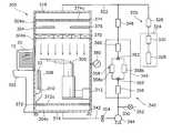
- FIG. 1illustrates a cross-sectional view of a module for transferring a substrate according to one embodiment of the present invention.
- FIG. 2illustrates a plan view of a substrate process apparatus having the substrate transfer module as shown in FIG. 1.
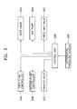
- FIG. 3is a block diagram illustrating operation of the substrate transfer module as shown in FIG. 1.
- FIG. 4illustrates a cross-sectional view of a module for transferring a substrate according to another embodiment of the present invention.
- FIG. 1illustrates a cross-sectional view of a module for transferring a substrate according to one embodiment of the present invention
- FIG. 2illustrates a plan view of a substrate process apparatus having the substrate transfer module as shown in FIG. 1.
- a substrate process apparatus 200performs some processes, for example, a deposition process for forming a layer on a semiconductor substrate 10 or an etching process for etching the layer on the semiconductor substrate 10 to form an electrical pattern on the semiconductor substrate 10 .
- the substrate process apparatus 200preferably includes a substrate process module 210 for processing the semiconductor substrate 10 , and a substrate transfer module 300 for transferring the semiconductor substrate 10 between a container for receiving a plurality of semiconductor substrates 10 and the substrate process module 210 .
- the containerpreferably includes a front opening unified pod (FOUP) 20 .
- FOUPfront opening unified pod
- a pair of load lock chambers 220is disposed between the substrate process module 210 and the substrate transfer module 300 .
- the substrate process module 210preferably includes a plurality of process chambers 230 for processing the semiconductor substrates 10 , a first substrate transfer chamber 240 for connecting between the load lock chambers 220 and the process chambers 230 , and a first substrate transfer robot 250 for transferring the semiconductor substrates 10 between the load lock chambers 220 and the process chambers 230 .
- the substrate transfer module 300preferably includes a load port 302 for supporting the FOUP 20 , a second substrate transfer chamber 304 disposed between the load port 302 and the load lock chambers 220 , a second substrate transfer robot 306 for transferring the semiconductor substrates 10 between the FOUP 20 and the load lock chambers 220 , a gas supply unit 320 for supplying a purge gas into the second substrate transfer chamber 304 in order to purge an interior of the second substrate transfer chamber 304 , and a contamination control unit 340 for preventing contamination of the semiconductor substrates 10 .
- the load port 302supports the FOUP 20 and brings a door 22 of the FOUP 20 into tight contact with a door 308 of the second substrate transfer chamber 304 .
- a door opener 310 for opening and closing the door 22 of the FOUP 20is provided in the second substrate transfer chamber 304 and is connected to the door 308 of the second substrate transfer chamber 304 .
- the door opener 310simultaneously opens the door 22 of the FOUP 20 and the door 308 of the second substrate transfer chamber 304 .
- the second substrate transfer robot 306is disposed to transfer the semiconductor substrates 10 in the second substrate transfer chamber 304 .
- a driving part 312 for moving the second substrate transfer robot 306 horizontallyis installed on an inner sidewall of the second substrate transfer chamber 304 , and the second substrate transfer robot 306 is connected to the driving part 312 .
- the second substrate transfer robot 306may be installed on a bottom panel 314 of the second substrate transfer chamber 304 . That is, although the second substrate transfer robot 306 shown in FIG. 1 is connected to the driving part 312 , numerous other configurations are possible.
- the gas supply unit 320is connected to an upper panel 316 of the second substrate transfer chamber 304 .
- the gas supply unit 320preferably includes a gas supply pipe 322 connected to the upper panel 316 , a gas source 324 for supplying the purge gas, and a first flow controller 326 for adjusting a flow rate of the purge gas supplied from the gas source 324 .
- a mass flow controllermay be used as the first flow controller 326 , and an inert gas such as nitrogen gas, argon gas or the like may be used as the purge gas.
- the gas supply unit 320preferably supplies the purge gas into the second substrate transfer chamber 304
- the gas source 324preferably includes a storage container 328 for storing the purge gas and a gas purifier 330 for purifying the purge gas. It is preferable that an oxygen content and a water content of nitrogen gas used as the purge gas are less than about 10 ppb.
- the gas purifier 330may include an area purifier, a bulk purifier or the like.
- the contamination control unit 340 connected to the second substrate transfer chamber 304circulates the purge gas supplied into the second substrate transfer chamber 304 , resupplies the circulated purge gas into the second substrate transfer chamber 304 , and removes particles and airborne molecular contaminants contained in the purge gas being circulated.
- the contamination control unit 340preferably includes a gas circular pipe 342 , an air pump 344 , a filtering part 346 , and a second flow controller 348 .
- the gas circular pipe 342is extended from the bottom panel 314 of the second substrate transfer chamber 304 , and is connected to the gas supply pipe 322 connected to the upper panel 316 of the second substrate transfer chamber 304 .
- the air pump 344is installed in the gas circular pipe 342 , sucks the purge gas supplied into the second substrate transfer chamber 304 through the gas circular pipe 342 , and circulates the sucked purge gas through the gas circular pipe 342 .
- the filtering part 346is installed in the gas circular pipe 342 , and removes the particles and the airborne molecular contaminants contained in the purge gas being circulated.
- the second flow controller 348adjusts a flow rate of the purge gas purified by the filtering part 346 .
- the contamination control unit 340further includes a gas exhaust pipe 350 , an exhaust valve 352 , and a gate valve 354 .
- the gas exhaust pipe 350is connected to the gas circular pipe 342 , and exhausts the nitrogen gas circulated by the air pump 344 .
- the exhaust valve 352is installed in the gas exhaust pipe 350 , and opens and closes the gas exhaust pipe 350 .
- the gate valve 354is installed in the circular pipe 342 between the second substrate transfer chamber 304 and the air pump 344 .
- a relief valvemay be used as the exhaust valve 352 .
- the relief valve used as the exhaust valve 352compares the pressure in the circular pipe 342 with a predetermined pressure, and adjusts the flow rate of the purge gas exhausted through the gas exhaust pipe 350 in accordance with a comparison result.
- a proportional control valvemay instead be used as the exhaust valve 352 . In this case, the proportional control valve adjusts the flow rate of the exhausted purge gas in accordance with the pressure in the circular pipe 342 .
- the exhaust valve 342may be controlled by a control unit (not shown) for adjusting an internal pressure in the second substrate transfer chamber 304 .
- gas exhaust pipe 350 and the exhaust valve 352are disposed between the air pump 344 and the filtering part 346 , in FIG. 1, various other configurations are possible.
- the gas exhaust pipe 350 and the exhaust valve 352may be disposed between the filtering part 346 and the second flow controller 348 .
- the gate valve 354When the air condition of the interior of the second substrate transfer chamber 304 is changed abruptly, the gate valve 354 is closed. For example, when a side panel of the second substrate transfer chamber 304 is opened for maintaining the substrate transfer module 300 , the gate valve 354 is closed so that the purge gas supplied into the second substrate transfer chamber 304 is exhausted through an open portion of the second substrate transfer chamber 304 . Accordingly, external air cannot flow into the second substrate transfer chamber 304 , thereby preventing contamination of the semiconductor substrates 10 by external air. Furthermore, external air is prevented from flowing into the air pump 344 and the filtering part 346 through the gas circular pipe 342 .
- the filtering part 346 for removing impurities contained in the purge gas, which is being circulated through the circular pipe 342preferably includes a first particle filter 356 for removing the particles, a moisture purifier 358 for removing moisture, and an organic contaminant filter 360 for removing organic contaminants such as a volatile organic compound (VOC).
- a first particle filter 356 for removing the particlespreferably includes a moisture purifier 358 for removing moisture, and an organic contaminant filter 360 for removing organic contaminants such as a volatile organic compound (VOC).
- VOCvolatile organic compound
- a high efficiency particulate air (HEPA) filter or an ultra low penetration air (ULPA) filtermay be used as the first particle filter 356 , and an activated carbon filter may be used as the organic contaminant filter 360 .
- a pair of molecular sieve moisture purifiers 358 a and 358 bmay be used as the moisture purifier 358 .
- the pair of molecular sieve moisture purifiers 358 a and 358 bis disposed between the first particle filter 356 and the organic contaminant filter 360 , and is connected in parallel to the gas circular pipe 342 through a pair of three-way valves 362 .
- a first molecular sieve moisture purifier 358 ais connected to the gas circular pipe 342
- a second molecular sieve moisture purifier 358 bis restored.
- the first molecular sieve moisture purifier 358 ais restored while the second molecular sieve moisture purifier 358 b is connected to the gas circular pipe 342 .
- the interior of the second substrate transfer chamber 304may be divided into an upper area 304 a connected with the gas supply pipe 322 , a lower area 304 c connected with the gas circular pipe 342 , and a substrate handling area 304 b for transferring the semiconductor substrates 10 between the upper area 304 a and the lower area 304 c.
- the upper area 304 a and the substrate handling area 304 bare divided by a second particle filter 370
- the substrate handling area 304 b and the lower area 304 care divided by a perforated panel 372 .
- a HEPA filter or an ULPA filtermay be used as the second particle filter 370 .
- a distribution panel 374is disposed in the upper area 304 a defined between the upper panel 316 of the second substrate transfer chamber 304 and the second particle filter 370 , and has a plurality of holes 374 a .
- the distribution panel 374uniformly provides the purge gas supplied from the gas supply unit 320 and the purge gas circulated through the gas circular pipe 342 into the substrate handling area 304 b.
- the purge gas supplied into the second substrate transfer chamber 304is dried by the gas purifier 330 of the gas supply unit 320 and the moisture purifier 358 of the contamination control unit 340 .
- An ionizer 376is disposed between the distribution panel 374 and the second particle filter 370 . The ionizer 376 removes static electricity from the semiconductor substrate 10 due to the dried purge gas.
- the second substrate transfer robot 306is disposed in the substrate handling area 304 b .
- the distribution panel 374forms a flow of the purge gas supplied through the gas supply pipe 322 into a laminar flow, and the perforated panel 372 assists function of the distribution panel 374 .
- the perforated panel 372has a plurality of holes 372 a similar to those of the distribution panel 374 . Accordingly, the second substrate transfer robot 306 can stably transfer the semiconductor substrate 10 .
- arrowsrepresent the laminar flow of the purge gas in the second substrate transfer chamber 304
- reference designator 380indicates a differential pressure sensor for measuring a differential pressure between an internal pressure and an external pressure of the second substrate transfer chamber 304 .
- FIG. 3is a block diagram illustrating operation of the substrate transfer module as shown in FIG. 1.
- the differential pressure sensor 380is connected to a control unit 390 .
- the elements already described in connection with the substrate transfer module 300 shown in FIG. 1are also connected to the control unit 390 .
- the differential pressure sensor 380measures the differential pressure between the internal pressure and the external pressure of the second substrate transfer chamber 304 , and sends the measured differential pressure to the control unit 390 .
- the control unit 390compares the measured differential pressure with a predetermined differential pressure, and controls operations of the first and second flow controllers 326 and 348 in accordance with a comparison result. For example, when the door 22 of the FOUP 20 is opened by the door opener 310 , the control unit 390 increases the flow rate of the purge gas from the gas supply unit 320 and decreases the flow rate of the purge gas circulated through the gas circular pipe 342 .
- the purge gas supplied from the gas supply unit 320purges an interior of the FOUP 20 , and air inside the FOUP 20 is exhausted through the gas exhaust pipe 350 and the exhaust valve 352 . Accordingly, the differential pressure is evenly maintained at the predetermined differential pressure.
- the control unit 390may suitably control an operation of the exhaust valve 352 installed in the gas exhaust pipe 350 . That is, the control unit 390 preferably adjusts the flow rate of purge gas exhausted through the gas exhaust pipe 350 .
- the control unit 390suitably controls the operations of the exhaust valve 352 and the second flow controller 348 , thereby adjusting the purge gas being circulated through the circular pipe 342 .
- control unit 390suitably controls operations of the air pump 344 and the gate valve 354 , thereby adjusting the flow rate of the circulated purge gas.
- the control unit 390closes the gate valve 354 , stops the operation of the air pump 344 and then increases the flow rate of purge gas being supplied from the gas supply unit 320 .
- the purge gas supplied into the second substrate 304is exhausted through the open portion of the second substrate transfer chamber 304 , and external air cannot flow into the second substrate transfer chamber 304 .
- control unit 390suitably controls operations of the pair of three-way valves 362 such that each of the pair of three-way valves is alternately connected with the gas circular pipe 342 .
- FIG. 4illustrates a cross-sectional view of a module for transferring a substrate according to another embodiment of the present invention.
- a substrate transfer module 400preferably includes a load port 402 for supporting a FOUP 20 , a substrate transfer chamber 404 disposed between the load port 402 and a load lock chamber (referring to FIG. 2), a substrate transfer robot 406 for transferring semiconductor substrates 10 between the FOUP 20 and the load lock chamber, a door opener 410 for opening and closing a door 22 of the FOUP 20 , a gas supply unit 420 for supplying purge gas in order to purge an interior of the substrate transfer chamber 404 , and a contamination control unit 440 for preventing contamination of the semiconductor substrates 10 .
- a driving part 412 for moving the second substrate transfer robot 306 horizontallyis installed on an inner sidewall of the second substrate transfer chamber 404 , and the second substrate transfer robot 406 is connected to the driving part 412 .
- the gas supply unit 420is connected to an upper panel 416 of the substrate transfer chamber 404 , and preferably includes a gas supply pipe 422 connected to the upper panel 416 , a gas source 424 for supplying the purge, and a first flow controller 426 for adjusting a flow rate of the purge gas.
- a MFCmay be used as the first flow controller 426 , and purified air may be used as the purge gas.
- the gas source 424preferably includes a storage container 428 for storing compressed air and a purifier for removing impurities contained in the air being supplied from the storage container.
- the purifierpreferably includes a first purifier 430 for primarily purifying the air and a second purifier 432 for secondarily purifying the primarily purified air.
- the first purifier 430removes water H 2 O and carbon dioxide CO 2 contained in the air being supplied from the storage container 428
- the second purifier 432removes water H 2 O, carbon monoxide CO, sulfur oxides SOx, nitrogen oxides NOx or the like contained in the primarily purified air.
- a molecular sieve purifier and a catalytic purifiermay be used as the first and second purifiers 430 and 432 , respectively.
- the contamination control unit 440is connected to the substrate transfer chamber 404 , circulates the air supplied into the substrate transfer chamber 404 , and then resupplies the circulated air into the substrate transfer chamber 404 . Also, the contamination control unit 440 removes particles and airborne molecular contaminants contained in the air being circulated.
- the contamination control unit 440preferably includes a gas circular pipe 442 , an air pump 444 , a filtering part 446 , and a second flow controller 448 .
- the gas circular pipe 442is extended from a bottom panel 414 of the substrate transfer chamber 404 , and is connected to the gas supply pipe 422 connected to the upper panel 416 of the substrate transfer chamber 404 .
- the air pump 444is installed in the gas circular pipe 442 , sucks the air supplied into the substrate transfer chamber 404 through the gas circular pipe 442 , and circulates the sucked air through the gas circular pipe 442 .
- the filtering part 446is installed in the gas circular pipe 442 , and removes particles and airborne molecular contaminants contained the air being circulated.
- the second flow controller 448adjusts a flow rate of the air purified by the filtering part 446 .
- the contamination control unit 440further includes a gas exhaust pipe 450 , an exhaust valve 452 and a gate valve 454 .
- the gas exhaust pipe 450is connected to the gas circular pipe 442 , and exhausts the air circulated by the air pump 444 .
- the exhaust valve 452is installed in the gas exhaust pipe 450
- the gate valve 454is installed in the circular pipe 442 between the second substrate transfer chamber 404 and the air pump 444 .
- the filtering part 446 for the impurities contained in the air being circulated through the circular pipe 442preferably includes a first particle filter 456 for removing the particles, a moisture purifier 458 for removing moisture, and an organic contaminant filter 460 for removing organic contaminants such as a volatile organic compound (VOC).
- a first particle filter 456for removing the particles
- a moisture purifier 458for removing moisture
- an organic contaminant filter 460for removing organic contaminants such as a volatile organic compound (VOC).
- a HEPA filter or an ULPA filtermay be used as the first particle filter 456 , and an activated carbon filter may be used as the organic contaminant filter 460 .
- a pair of molecular sieve moisture 458 a and 458 bmay be used as the moisture purifier 458 .
- the pair of molecular sieve moisture purifiers 458 a and 458 bis disposed between the first particle filter 456 and the organic contaminant filter 460 , and is connected in parallel to the circular pipe 442 through a pair of three-way valves 462 .
- the interior of the substrate transfer chamber 404may be divided into an upper area 404 a , a substrate handling area 404 b and a lower area 404 c.
- a distribution panel 474 having a plurality of holes 474 ais disposed in the upper area 404 a .
- the distribution panel 474uniformly provides the air supplied from the gas supply unit 420 and the air circulated through the gas circular pipe 442 into the substrate handling area 404 b.
- An ionizer 476is disposed between the distribution panel 474 and a second particle filter 470 .
- the ionizer 476removes static electricity from the semiconductor substrate 10 due to the dry air supplied into the substrate transfer chamber 404 .
- a photo catalyst filter 478 for removing organic contaminants and an ultraviolet lamp 480 for applying ultraviolet rays onto the photo catalyst filter 478are disposed between the ionizer 476 and the second particle filter 470 .
- An aluminum Al mesh coated with titanium dioxide TiO 2may be used as the photo catalyst filter 478 , and it is preferable that the ultraviolet rays irradiated from the ultraviolet lamp 480 have a wavelength of 254 nm or longer.
- the ionizer 476 and the photo catalyst filter 478cause ozone to generate from the air supplied through the gas supply pipe 422 .
- the ozonemay be removed by means of an ozone filter 482 disposed between the photo catalyst filter 478 and the second particle filter 470 .
- the substrate transfer robot 406is disposed in the substrate handling area 404 b .
- the distribution panel 474forms a flow of the air supplied through the gas supply pipe 422 into a laminar flow, and a perforated panel 472 assists function of the distribution panel 474 .
- the perforated panel 472has a plurality of holes 472 a similar to those of the distribution panel 474 . Accordingly, the substrate transfer robot 406 can stably transfer the semiconductor substrate 10 .
- arrowsrepresent the laminar flow of the air in the substrate transfer chamber 404
- the reference designators 408 and 484indicate a door of the substrate transfer chamber 404 and a differential pressure sensor for measuring a differential pressure between an internal pressure and an external pressure of the second substrate transfer chamber 404 , respectively.
- a control unitcontrols operations of the elements of the substrate transfer module 400 , based on the differential pressure measured by the differential pressure sensor 484 .
- the purge gas supplied from the gas supply unitpurges the interior of the substrate transfer chamber.
- the contamination control unitcirculates and purifies the purge gas supplied into the substrate transfer chamber, and then resupplies the circulated/purified purge gas into the substrate transfer chamber.
Landscapes
- Engineering & Computer Science (AREA)
- Physics & Mathematics (AREA)
- Condensed Matter Physics & Semiconductors (AREA)
- General Physics & Mathematics (AREA)
- Manufacturing & Machinery (AREA)
- Computer Hardware Design (AREA)
- Microelectronics & Electronic Packaging (AREA)
- Power Engineering (AREA)
- Container, Conveyance, Adherence, Positioning, Of Wafer (AREA)
Abstract
Description
- 1. Field of the Invention[0001]
- The present invention is related to a module for transferring a substrate. More particularly, the present invention is related to a module for transferring a substrate between a container to receive a plurality of substrates and a module for processing the substrate.[0002]
- 2. Description of the Related Art[0003]
- Generally, semiconductor devices are manufactured through a three-step process. First, a fabrication process is performed for forming electronic circuits on a silicon wafer used as a semiconductor substrate. Second, an electrical die sorting (EDS) process is performed for inspecting electrical characteristics of the semiconductor devices on the semiconductor substrate. Third, a packaging process is performed for packaging the semiconductor devices in epoxy resins and individuating the semiconductor devices.[0004]
- The fabrication process may include a deposition process for depositing a layer on the substrate, a chemical mechanical polishing (CMP) process for planarizing a surface of the layer, a photolithography process for forming a photoresist pattern on the layer, an etching process for an electrical pattern using the photoresist pattern, an ion implantation process for implanting predetermined ions into predetermined portions of the substrate, a cleaning process for removing impurities from the substrate, an inspection process for inspecting the surface of the substrate on which the layer or the pattern is formed, or other similar processes.[0005]
- These processes are performed under a high vacuum condition in order to prevent contamination of the semiconductor substrate. To provide the high vacuum condition, a substrate process apparatus includes a load lock chamber maintained under a low vacuum condition, a process chamber in which the process is performed, and a substrate transfer chamber for transferring the semiconductor substrate between the load lock chamber and the process chamber.[0006]
- Recently, a substrate process apparatus for some processes (for example, a deposition process or a dry etching process) on a 300 mm semiconductor substrate includes a substrate process module, a substrate transfer module and a load lock chamber. The substrate transfer module includes a load port for supporting a front opening unified pod (FOUP), a substrate transfer chamber disposed between the load port and the load lock chamber, and a substrate transfer robot for transferring the semiconductor substrate between the FOUP and the load lock chamber.[0007]
- A fan filter unit (FFU) is connected to an upper portion of the substrate transfer chamber. The fan filter unit supplies an interior of the substrate transfer chamber with clean air for preventing contamination of the semiconductor substrate being transferred by the substrate transfer robot.[0008]
- A plurality of exhaust holes is formed through a bottom panel of the substrate transfer chamber in order to exhaust the clean air supplied from the fan filter unit out of the substrate transfer chamber or to a clean room in which the substrate process apparatus is provided.[0009]
- When an internal pressure of the substrate transfer chamber is lower than a pressure of the clean room, the air in the clean room may flow back into the substrate transfer chamber, so that the semiconductor substrates received in the FOUP and the semiconductor substrate being transferred by the substrate transfer robot may be contaminated. Therefore, it is preferable to maintain the internal pressure of the substrate transfer chamber higher than the pressure of the clean room. The pressure of the clean room, in which the substrate process apparatus is provided, is generally a positive pressure (i.e., higher than atmospheric pressure).[0010]
- For example, a multichamber processing system including a container-housing chamber, a cleaning chamber and a load lock chamber is disclosed in the prior art. The cleaning chamber has an inlet line for introducing a clean gas into the cleaning chamber and a pressure control device for controlling the pressure in the cleaning chamber. The pressure control device includes a valve for adjusting a flow rate of the gas in the inlet line, a differential pressure gauge for detecting a differential pressure between the pressure in the cleaning chamber and the atmospheric pressure, and a valve controller for adjusting an opening degree of the valve so that the pressure in the cleaning chamber is maintained at the positive pressure based on a result of the detecting by the differential pressure gauge.[0011]
- In addition, wafer atmospheric transport module having a controlled mini-environment is disclosed in the prior art. According to this example, a blower located in the top region of an enclosed housing is configured to generate a flow of air downward. The airflow generated by the blower is restricted from freely flowing through a perforated sheet and is partially induced to be redirected toward the shelf, and a cassette having one or more wafers is configured to sit on a shelf in the enclosed housing and thus be subjected to the redirected air flow.[0012]
- The fan filter unit includes a fan for supplying external air into the substrate transfer chamber and a filter for removing particles contained in the external air being supplied into the substrate transfer chamber. However, the filter cannot remove airborne molecular contaminants, such as organic contaminants, contained in the external air being supplied into the substrate transfer chamber. Such airborne molecular contaminants may cause various defects on the semiconductor substrate.[0013]
- Examples of the defects may include a variation of a critical dimension (CD) of a photochemical amplified resist pattern and T-top defect caused by ammonia, a natural oxide layer generated by ozone, condensational contaminants or the like. Variation of the critical dimension of the photochemical amplified resist pattern and T-top defect may be detected in the fabrication process, and operation failure of electrical circuit elements such as transistors due to organic contaminants such as dioctyl phthalate (DOP) may be detected in the electrical die sorting process.[0014]
- To solve these and other problems, the present invention provides a module for transferring a substrate that prevents the substrate from being contaminated by impurities including particles and airborne molecular contaminants during transfer of the substrate between a FOUP and a substrate process module.[0015]
- According to a feature of an embodiment of the present invention, there is provides a module for transferring a substrate including a load port for supporting a container to receive a plurality of substrates, a substrate transfer chamber disposed between the load port and a substrate process module for processing the substrates, a substrate transfer robot disposed in the substrate transfer chamber for transferring the substrates between the container and the substrate process module, a gas supply unit connected to the substrate transfer chamber for supplying a purge gas into the substrate transfer chamber so as to purge an interior of the substrate transfer chamber, and a contamination control unit connected to the substrate transfer chamber for circulating the purge gas supplied into the substrate transfer chamber, resupplying the circulated purge gas into the substrate transfer chamber and removing particles and airborne molecular contaminants from the purge gas being circulated.[0016]
- In the module, the container preferably includes a front opening unified pod (FOUP). The module may further include a door opener for opening and closing a door of the FOUP. Also in the module, the gas supply unit may include a gas source for providing the purge gas, a gas supply pipe for connecting the gas source and the substrate transfer chamber, and a flow controller installed in the gas supply pipe for adjusting a flow rate of the purge gas being supplied into the substrate transfer chamber.[0017]
- The purge gas may include a nitrogen gas, and the gas source may include a storage container for storing the nitrogen gas and a purifier for purifying the nitrogen gas. Alternatively, the purge gas may include air, and the gas source may include a storage container for storing compressed air and a purifier for removing impurities contained in the air being supplied from the storage container. The purifier preferably includes a molecular sieve purifier or a catalytic purifier.[0018]
- The contamination control unit may include a gas circular pipe connecting an upper portion and a lower portion of the substrate transfer chamber, an air pump installed in the gas circular pipe for sucking the purge gas supplied into the substrate transfer chamber and circulating the sucked purge gas through the gas circular pipe, a filtering part installed in the gas circular pipe for removing the particles and the airborne molecular contaminants contained in the purge gas being circulated, and a flow controller installed in the gas circular pipe for controlling a flow rate of the purge gas being circulated.[0019]
- The contamination control unit may further include a gas exhaust pipe connected to the gas circular pipe for exhausting the purge gas being circulated and a valve installed in the gas exhaust pipe for opening and closing the gas exhaust pipe.[0020]
- The contamination control unit may further include a valve installed in the gas circular pipe between the lower portion of the substrate transfer chamber and the air pump for opening and closing the gas circular pipe.[0021]
- The filtering part may include a particle filter for removing the particles contained in the purge gas being circulated, a moisture purifier for removing moisture contained in the purge gas being circulated, and an organic contaminant filter for removing organic contaminants contained in the purge gas being circulated. The moisture purifier is preferably a molecular sieve moisture purifier; the organic contaminant filter is preferably an activated carbon filter.[0022]
- The module may further include a distribution panel horizontally disposed in the substrate transfer chamber, the distribution panel having a plurality of holes for uniformly supplying the purge gas into the substrate transfer chamber, and a particle filter disposed between the distribution panel and the substrate transfer robot for removing particles contained in the purge gas being supplied through the holes of the distribution panel.[0023]
- Also, an ionizer may be disposed between the distribution panel and the particle filter for removing static electricity from the substrates.[0024]
- The purge gas may be an inert gas, and the inert gas may be a nitrogen gas. Alternatively, the purge gas may be purified air.[0025]
- A photo catalyst filter may be disposed between the distribution panel and the particle filter for removing organic contaminants contained in the purge gas being supplied into the substrate transfer chamber, and an ultraviolet lamp for applying ultraviolet rays onto the photo catalyst filter. An ozone filter may be disposed between the photo catalyst filter and the particle filter for removing ozone contained in the purge gas being supplied into the substrate transfer chamber.[0026]
- A differential pressure sensor may be connected to the substrate transfer chamber for measuring a differential pressure between an internal pressure and an external pressure of the substrate transfer chamber and a control unit for comparing the differential pressure measured by the differential pressure sensor with a predetermined differential pressure, and for adjusting a flow rate of the purge gas being supplied into the substrate transfer chamber and a flow rate of the purge gas being circulated through the contamination control unit in accordance with a comparison result.[0027]
- A perforated panel may be disposed above a bottom panel of the substrate transfer chamber for passing the purge gas supplied into the substrate transfer chamber therethrough, wherein the perforated panel has a plurality of holes, and the contamination control unit is connected to the bottom panel of the substrate transfer chamber.[0028]
- The interior of the substrate transfer chamber is purged by the purge gas supplied from the gas supply unit and the resupplied purge gas from the contamination control unit, and thus impurities including particles and airborne molecular contaminants do not flow into the substrate transfer chamber. As a result, contamination of the substrate due to the impurities may be prevented.[0029]
- In addition, the purge gas supplied into the substrate transfer chamber is circulated by means of the contamination control unit, and thus an amount of the purge gas used in the substrate transfer module may be reduced.[0030]
- The above and other features and advantages of the present invention will become more apparent to those of ordinary skill in the art by describing in detail preferred embodiments thereof with reference to the attached drawings in which:[0031]
- FIG. 1 illustrates a cross-sectional view of a module for transferring a substrate according to one embodiment of the present invention.[0032]
- FIG. 2 illustrates a plan view of a substrate process apparatus having the substrate transfer module as shown in FIG. 1.[0033]
- FIG. 3 is a block diagram illustrating operation of the substrate transfer module as shown in FIG. 1.[0034]
- FIG. 4 illustrates a cross-sectional view of a module for transferring a substrate according to another embodiment of the present invention.[0035]
- Korean Patent Application No. 2003-8847, filed on Feb. 12, 2003, and entitled: “Module For Transferring A Substrate,” is incorporated by reference herein in its entirety.[0036]
- The present invention will now be described more fully hereinafter with reference to the accompanying drawings, in which preferred embodiments of the invention are shown. The invention may, however, be embodied in different forms and should not be construed as limited to the embodiments set forth herein. Rather, these embodiments are provided so that this disclosure will be thorough and complete, and will fully convey the scope of the invention to those skilled in the art. Like numbers refer to like elements throughout.[0037]
- FIG. 1 illustrates a cross-sectional view of a module for transferring a substrate according to one embodiment of the present invention, and FIG. 2 illustrates a plan view of a substrate process apparatus having the substrate transfer module as shown in FIG. 1.[0038]
- Referring to FIGS. 1 and 2, a[0039]
substrate process apparatus 200 performs some processes, for example, a deposition process for forming a layer on asemiconductor substrate 10 or an etching process for etching the layer on thesemiconductor substrate 10 to form an electrical pattern on thesemiconductor substrate 10. Thesubstrate process apparatus 200 preferably includes asubstrate process module 210 for processing thesemiconductor substrate 10, and asubstrate transfer module 300 for transferring thesemiconductor substrate 10 between a container for receiving a plurality ofsemiconductor substrates 10 and thesubstrate process module 210. The container preferably includes a front opening unified pod (FOUP)20. - A pair of[0040]
load lock chambers 220 is disposed between thesubstrate process module 210 and thesubstrate transfer module 300. - The[0041]
substrate process module 210 preferably includes a plurality ofprocess chambers 230 for processing thesemiconductor substrates 10, a firstsubstrate transfer chamber 240 for connecting between theload lock chambers 220 and theprocess chambers 230, and a firstsubstrate transfer robot 250 for transferring thesemiconductor substrates 10 between theload lock chambers 220 and theprocess chambers 230. - The[0042]
substrate transfer module 300 preferably includes aload port 302 for supporting theFOUP 20, a secondsubstrate transfer chamber 304 disposed between theload port 302 and theload lock chambers 220, a secondsubstrate transfer robot 306 for transferring thesemiconductor substrates 10 between theFOUP 20 and theload lock chambers 220, agas supply unit 320 for supplying a purge gas into the secondsubstrate transfer chamber 304 in order to purge an interior of the secondsubstrate transfer chamber 304, and acontamination control unit 340 for preventing contamination of thesemiconductor substrates 10. - Although not shown in detail, the[0043]
load port 302 supports theFOUP 20 and brings adoor 22 of theFOUP 20 into tight contact with adoor 308 of the secondsubstrate transfer chamber 304. Adoor opener 310 for opening and closing thedoor 22 of theFOUP 20 is provided in the secondsubstrate transfer chamber 304 and is connected to thedoor 308 of the secondsubstrate transfer chamber 304. Thedoor opener 310 simultaneously opens thedoor 22 of theFOUP 20 and thedoor 308 of the secondsubstrate transfer chamber 304. - The second[0044]
substrate transfer robot 306 is disposed to transfer thesemiconductor substrates 10 in the secondsubstrate transfer chamber 304. A drivingpart 312 for moving the secondsubstrate transfer robot 306 horizontally is installed on an inner sidewall of the secondsubstrate transfer chamber 304, and the secondsubstrate transfer robot 306 is connected to the drivingpart 312. However, the secondsubstrate transfer robot 306 may be installed on abottom panel 314 of the secondsubstrate transfer chamber 304. That is, although the secondsubstrate transfer robot 306 shown in FIG. 1 is connected to the drivingpart 312, numerous other configurations are possible. - The[0045]
gas supply unit 320 is connected to anupper panel 316 of the secondsubstrate transfer chamber 304. Thegas supply unit 320 preferably includes agas supply pipe 322 connected to theupper panel 316, agas source 324 for supplying the purge gas, and afirst flow controller 326 for adjusting a flow rate of the purge gas supplied from thegas source 324. - A mass flow controller (MFC) may be used as the[0046]
first flow controller 326, and an inert gas such as nitrogen gas, argon gas or the like may be used as the purge gas. - The[0047]
gas supply unit 320 preferably supplies the purge gas into the secondsubstrate transfer chamber 304, and thegas source 324 preferably includes astorage container 328 for storing the purge gas and agas purifier 330 for purifying the purge gas. It is preferable that an oxygen content and a water content of nitrogen gas used as the purge gas are less than about 10 ppb. Examples of thegas purifier 330 may include an area purifier, a bulk purifier or the like. - The[0048]
contamination control unit 340 connected to the secondsubstrate transfer chamber 304 circulates the purge gas supplied into the secondsubstrate transfer chamber 304, resupplies the circulated purge gas into the secondsubstrate transfer chamber 304, and removes particles and airborne molecular contaminants contained in the purge gas being circulated. - The[0049]
contamination control unit 340 preferably includes a gascircular pipe 342, anair pump 344, afiltering part 346, and asecond flow controller 348. The gascircular pipe 342 is extended from thebottom panel 314 of the secondsubstrate transfer chamber 304, and is connected to thegas supply pipe 322 connected to theupper panel 316 of the secondsubstrate transfer chamber 304. Theair pump 344 is installed in the gascircular pipe 342, sucks the purge gas supplied into the secondsubstrate transfer chamber 304 through the gascircular pipe 342, and circulates the sucked purge gas through the gascircular pipe 342. Thefiltering part 346 is installed in the gascircular pipe 342, and removes the particles and the airborne molecular contaminants contained in the purge gas being circulated. Thesecond flow controller 348 adjusts a flow rate of the purge gas purified by thefiltering part 346. - The[0050]
contamination control unit 340 further includes agas exhaust pipe 350, anexhaust valve 352, and agate valve 354. Thegas exhaust pipe 350 is connected to the gascircular pipe 342, and exhausts the nitrogen gas circulated by theair pump 344. Theexhaust valve 352 is installed in thegas exhaust pipe 350, and opens and closes thegas exhaust pipe 350. Thegate valve 354 is installed in thecircular pipe 342 between the secondsubstrate transfer chamber 304 and theair pump 344. A relief valve may be used as theexhaust valve 352. - When the flow rate of the circulated purge gas is reduced by operation of the[0051]
second flow controller 348, pressure in thecircular pipe 342 is gradually increased. At that time, the relief valve used as theexhaust valve 352 compares the pressure in thecircular pipe 342 with a predetermined pressure, and adjusts the flow rate of the purge gas exhausted through thegas exhaust pipe 350 in accordance with a comparison result. A proportional control valve may instead be used as theexhaust valve 352. In this case, the proportional control valve adjusts the flow rate of the exhausted purge gas in accordance with the pressure in thecircular pipe 342. Alternatively, theexhaust valve 342 may be controlled by a control unit (not shown) for adjusting an internal pressure in the secondsubstrate transfer chamber 304. - Although the[0052]
gas exhaust pipe 350 and theexhaust valve 352 are disposed between theair pump 344 and thefiltering part 346, in FIG. 1, various other configurations are possible. For example, thegas exhaust pipe 350 and theexhaust valve 352 may be disposed between thefiltering part 346 and thesecond flow controller 348. - When the air condition of the interior of the second[0053]
substrate transfer chamber 304 is changed abruptly, thegate valve 354 is closed. For example, when a side panel of the secondsubstrate transfer chamber 304 is opened for maintaining thesubstrate transfer module 300, thegate valve 354 is closed so that the purge gas supplied into the secondsubstrate transfer chamber 304 is exhausted through an open portion of the secondsubstrate transfer chamber 304. Accordingly, external air cannot flow into the secondsubstrate transfer chamber 304, thereby preventing contamination of thesemiconductor substrates 10 by external air. Furthermore, external air is prevented from flowing into theair pump 344 and thefiltering part 346 through the gascircular pipe 342. - The[0054]
filtering part 346 for removing impurities contained in the purge gas, which is being circulated through thecircular pipe 342, preferably includes afirst particle filter 356 for removing the particles, amoisture purifier 358 for removing moisture, and anorganic contaminant filter 360 for removing organic contaminants such as a volatile organic compound (VOC). - A high efficiency particulate air (HEPA) filter or an ultra low penetration air (ULPA) filter may be used as the[0055]
first particle filter 356, and an activated carbon filter may be used as theorganic contaminant filter 360. A pair of molecularsieve moisture purifiers moisture purifier 358. - As shown in FIG. 1, the pair of molecular[0056]
sieve moisture purifiers first particle filter 356 and theorganic contaminant filter 360, and is connected in parallel to the gascircular pipe 342 through a pair of three-way valves 362. When a first molecularsieve moisture purifier 358ais connected to the gascircular pipe 342, a second molecularsieve moisture purifier 358bis restored. In contrast, the first molecularsieve moisture purifier 358ais restored while the second molecularsieve moisture purifier 358bis connected to the gascircular pipe 342. - The interior of the second[0057]
substrate transfer chamber 304 may be divided into anupper area 304aconnected with thegas supply pipe 322, alower area 304cconnected with the gascircular pipe 342, and asubstrate handling area 304bfor transferring thesemiconductor substrates 10 between theupper area 304aand thelower area 304c. - The[0058]
upper area 304aand thesubstrate handling area 304bare divided by asecond particle filter 370, and thesubstrate handling area 304band thelower area 304care divided by aperforated panel 372. A HEPA filter or an ULPA filter may be used as thesecond particle filter 370. - A[0059]
distribution panel 374 is disposed in theupper area 304adefined between theupper panel 316 of the secondsubstrate transfer chamber 304 and thesecond particle filter 370, and has a plurality ofholes 374a. Thedistribution panel 374 uniformly provides the purge gas supplied from thegas supply unit 320 and the purge gas circulated through the gascircular pipe 342 into thesubstrate handling area 304b. - The purge gas supplied into the second[0060]
substrate transfer chamber 304 is dried by thegas purifier 330 of thegas supply unit 320 and themoisture purifier 358 of thecontamination control unit 340. Anionizer 376 is disposed between thedistribution panel 374 and thesecond particle filter 370. Theionizer 376 removes static electricity from thesemiconductor substrate 10 due to the dried purge gas. - The second[0061]
substrate transfer robot 306 is disposed in thesubstrate handling area 304b. As shown in FIG. 1, thedistribution panel 374 forms a flow of the purge gas supplied through thegas supply pipe 322 into a laminar flow, and theperforated panel 372 assists function of thedistribution panel 374. Theperforated panel 372 has a plurality ofholes 372asimilar to those of thedistribution panel 374. Accordingly, the secondsubstrate transfer robot 306 can stably transfer thesemiconductor substrate 10. - In FIG. 1, arrows represent the laminar flow of the purge gas in the second[0062]
substrate transfer chamber 304, andreference designator 380 indicates a differential pressure sensor for measuring a differential pressure between an internal pressure and an external pressure of the secondsubstrate transfer chamber 304. - FIG. 3 is a block diagram illustrating operation of the substrate transfer module as shown in FIG. 1.[0063]
- Referring to FIGS. 1 and 3, the[0064]
differential pressure sensor 380 is connected to acontrol unit 390. The elements already described in connection with thesubstrate transfer module 300 shown in FIG. 1 are also connected to thecontrol unit 390. - The[0065]
differential pressure sensor 380 measures the differential pressure between the internal pressure and the external pressure of the secondsubstrate transfer chamber 304, and sends the measured differential pressure to thecontrol unit 390. Thecontrol unit 390 compares the measured differential pressure with a predetermined differential pressure, and controls operations of the first andsecond flow controllers door 22 of theFOUP 20 is opened by thedoor opener 310, thecontrol unit 390 increases the flow rate of the purge gas from thegas supply unit 320 and decreases the flow rate of the purge gas circulated through the gascircular pipe 342. The purge gas supplied from thegas supply unit 320 purges an interior of theFOUP 20, and air inside theFOUP 20 is exhausted through thegas exhaust pipe 350 and theexhaust valve 352. Accordingly, the differential pressure is evenly maintained at the predetermined differential pressure. - The[0066]
control unit 390 may suitably control an operation of theexhaust valve 352 installed in thegas exhaust pipe 350. That is, thecontrol unit 390 preferably adjusts the flow rate of purge gas exhausted through thegas exhaust pipe 350. For example, thecontrol unit 390 suitably controls the operations of theexhaust valve 352 and thesecond flow controller 348, thereby adjusting the purge gas being circulated through thecircular pipe 342. - In addition, the[0067]
control unit 390 suitably controls operations of theair pump 344 and thegate valve 354, thereby adjusting the flow rate of the circulated purge gas. For example, when the side panel of the secondsubstrate transfer chamber 304 is opened for maintenance of thesubstrate transfer module 300, thecontrol unit 390 closes thegate valve 354, stops the operation of theair pump 344 and then increases the flow rate of purge gas being supplied from thegas supply unit 320. As a result, the purge gas supplied into thesecond substrate 304 is exhausted through the open portion of the secondsubstrate transfer chamber 304, and external air cannot flow into the secondsubstrate transfer chamber 304. - Furthermore, the[0068]
control unit 390 suitably controls operations of the pair of three-way valves 362 such that each of the pair of three-way valves is alternately connected with the gascircular pipe 342. - FIG. 4 illustrates a cross-sectional view of a module for transferring a substrate according to another embodiment of the present invention.[0069]
- Referring to FIG. 4, a[0070]
substrate transfer module 400 preferably includes aload port 402 for supporting aFOUP 20, asubstrate transfer chamber 404 disposed between theload port 402 and a load lock chamber (referring to FIG. 2), asubstrate transfer robot 406 for transferringsemiconductor substrates 10 between theFOUP 20 and the load lock chamber, adoor opener 410 for opening and closing adoor 22 of theFOUP 20, agas supply unit 420 for supplying purge gas in order to purge an interior of thesubstrate transfer chamber 404, and acontamination control unit 440 for preventing contamination of thesemiconductor substrates 10. - A driving[0071]
part 412 for moving the secondsubstrate transfer robot 306 horizontally is installed on an inner sidewall of the secondsubstrate transfer chamber 404, and the secondsubstrate transfer robot 406 is connected to the drivingpart 412. - The[0072]
gas supply unit 420 is connected to anupper panel 416 of thesubstrate transfer chamber 404, and preferably includes agas supply pipe 422 connected to theupper panel 416, agas source 424 for supplying the purge, and afirst flow controller 426 for adjusting a flow rate of the purge gas. - A MFC may be used as the[0073]
first flow controller 426, and purified air may be used as the purge gas. - The[0074]
gas source 424 preferably includes astorage container 428 for storing compressed air and a purifier for removing impurities contained in the air being supplied from the storage container. The purifier preferably includes afirst purifier 430 for primarily purifying the air and asecond purifier 432 for secondarily purifying the primarily purified air. - The[0075]
first purifier 430 removes water H2O and carbon dioxide CO2contained in the air being supplied from thestorage container 428, and thesecond purifier 432 removes water H2O, carbon monoxide CO, sulfur oxides SOx, nitrogen oxides NOx or the like contained in the primarily purified air. A molecular sieve purifier and a catalytic purifier may be used as the first andsecond purifiers - The[0076]
contamination control unit 440 is connected to thesubstrate transfer chamber 404, circulates the air supplied into thesubstrate transfer chamber 404, and then resupplies the circulated air into thesubstrate transfer chamber 404. Also, thecontamination control unit 440 removes particles and airborne molecular contaminants contained in the air being circulated. - The[0077]
contamination control unit 440 preferably includes a gascircular pipe 442, anair pump 444, afiltering part 446, and asecond flow controller 448. The gascircular pipe 442 is extended from abottom panel 414 of thesubstrate transfer chamber 404, and is connected to thegas supply pipe 422 connected to theupper panel 416 of thesubstrate transfer chamber 404. Theair pump 444 is installed in the gascircular pipe 442, sucks the air supplied into thesubstrate transfer chamber 404 through the gascircular pipe 442, and circulates the sucked air through the gascircular pipe 442. Thefiltering part 446 is installed in the gascircular pipe 442, and removes particles and airborne molecular contaminants contained the air being circulated. Thesecond flow controller 448 adjusts a flow rate of the air purified by thefiltering part 446. - The[0078]
contamination control unit 440 further includes agas exhaust pipe 450, anexhaust valve 452 and agate valve 454. Thegas exhaust pipe 450 is connected to the gascircular pipe 442, and exhausts the air circulated by theair pump 444. Theexhaust valve 452 is installed in thegas exhaust pipe 450, and thegate valve 454 is installed in thecircular pipe 442 between the secondsubstrate transfer chamber 404 and theair pump 444. - The[0079]
filtering part 446 for the impurities contained in the air being circulated through thecircular pipe 442 preferably includes afirst particle filter 456 for removing the particles, amoisture purifier 458 for removing moisture, and anorganic contaminant filter 460 for removing organic contaminants such as a volatile organic compound (VOC). - A HEPA filter or an ULPA filter may be used as the[0080]
first particle filter 456, and an activated carbon filter may be used as theorganic contaminant filter 460. A pair ofmolecular sieve moisture moisture purifier 458. - As shown in FIG. 4, the pair of molecular[0081]
sieve moisture purifiers first particle filter 456 and theorganic contaminant filter 460, and is connected in parallel to thecircular pipe 442 through a pair of three-way valves 462. - The interior of the[0082]
substrate transfer chamber 404 may be divided into anupper area 404a, asubstrate handling area 404band alower area 404c. - A[0083]
distribution panel 474 having a plurality ofholes 474ais disposed in theupper area 404a. Thedistribution panel 474 uniformly provides the air supplied from thegas supply unit 420 and the air circulated through the gascircular pipe 442 into thesubstrate handling area 404b. - An[0084]
ionizer 476 is disposed between thedistribution panel 474 and asecond particle filter 470. Theionizer 476 removes static electricity from thesemiconductor substrate 10 due to the dry air supplied into thesubstrate transfer chamber 404. - A[0085]
photo catalyst filter 478 for removing organic contaminants and anultraviolet lamp 480 for applying ultraviolet rays onto thephoto catalyst filter 478 are disposed between theionizer 476 and thesecond particle filter 470. An aluminum Al mesh coated with titanium dioxide TiO2may be used as thephoto catalyst filter 478, and it is preferable that the ultraviolet rays irradiated from theultraviolet lamp 480 have a wavelength of 254 nm or longer. - The[0086]
ionizer 476 and thephoto catalyst filter 478 cause ozone to generate from the air supplied through thegas supply pipe 422. The ozone may be removed by means of anozone filter 482 disposed between thephoto catalyst filter 478 and thesecond particle filter 470. - The[0087]
substrate transfer robot 406 is disposed in thesubstrate handling area 404b. Thedistribution panel 474 forms a flow of the air supplied through thegas supply pipe 422 into a laminar flow, and aperforated panel 472 assists function of thedistribution panel 474. Theperforated panel 472 has a plurality ofholes 472asimilar to those of thedistribution panel 474. Accordingly, thesubstrate transfer robot 406 can stably transfer thesemiconductor substrate 10. - In FIG. 4, arrows represent the laminar flow of the air in the[0088]
substrate transfer chamber 404, and thereference designators substrate transfer chamber 404 and a differential pressure sensor for measuring a differential pressure between an internal pressure and an external pressure of the secondsubstrate transfer chamber 404, respectively. - Although not shown in figure, a control unit controls operations of the elements of the[0089]
substrate transfer module 400, based on the differential pressure measured by thedifferential pressure sensor 484. - Further detailed descriptions of these elements will be omitted because these elements are similar to those already described in connection with the[0090]
substrate transfer module 300 shown in FIGS. 1 and 2. - According to certain embodiments of the present invention, the purge gas supplied from the gas supply unit purges the interior of the substrate transfer chamber. The contamination control unit circulates and purifies the purge gas supplied into the substrate transfer chamber, and then resupplies the circulated/purified purge gas into the substrate transfer chamber.[0091]
- Accordingly, external air cannot flow into the substrate transfer chamber, thereby preventing contamination of the semiconductor substrate due to impurities contained in the external air. Furthermore, circulation of the purge gas reduces an amount of purge gas to be supplied from a source.[0092]
- Preferred embodiments of the present invention have been disclosed herein and, although specific terms are employed, they are used and are to be interpreted in a generic and descriptive sense only and not for purpose of limitation. Accordingly, it will be understood by those of ordinary skill in the art that various changes in form and details may be made without departing from the spirit and scope of the present invention as set forth in the following claims.[0093]
Claims (22)
1. A module for transferring a substrate comprising:
a load port for supporting a container to receive a plurality of substrates;
a substrate transfer chamber disposed between the load port and a substrate process module for processing the substrates;
a substrate transfer robot disposed in the substrate transfer chamber for transferring the substrates between the container and the substrate process module;
a gas supply unit connected to the substrate transfer chamber for supplying a purge gas into the substrate transfer chamber so as to purge an interior of the substrate transfer chamber; and
a contamination control unit connected to the substrate transfer chamber for circulating the purge gas supplied into the substrate transfer chamber, resupplying the circulated purge gas into the substrate transfer chamber and removing particles and airborne molecular contaminants from the purge gas being circulated.
2. The module as claimed inclaim 1 , wherein the container includes a front opening unified pod (FOUP).
3. The module as claimed inclaim 2 , further comprising a door opener for opening and closing a door of the FOUP.
4. The module as claimed inclaim 1 , wherein the gas supply unit includes:
a gas source for providing the purge gas;
a gas supply pipe for connecting the gas source and the substrate transfer chamber; and
a flow controller installed in the gas supply pipe for adjusting a flow rate of the purge gas being supplied into the substrate transfer chamber.
5. The module as claimed inclaim 4 , wherein the purge gas includes a nitrogen gas, and the gas source includes a storage container for storing the nitrogen gas and a purifier for purifying the nitrogen gas.
6. The module as claimed inclaim 4 , wherein the purge gas includes air, and the gas source includes a storage container for storing compressed air and a purifier for removing impurities contained in the air being supplied from the storage container.
7. The module as claimed inclaim 6 , wherein the purifier includes a molecular sieve purifier or a catalytic purifier.
8. The module as claimed inclaim 1 , wherein the contamination control unit includes:
a gas circular pipe connecting an upper portion and a lower portion of the substrate transfer chamber;
an air pump installed in the gas circular pipe for sucking the purge gas supplied into the substrate transfer chamber and circulating the sucked purge gas through the gas circular pipe;
a filtering part installed in the gas circular pipe for removing the particles and the airborne molecular contaminants contained in the purge gas being circulated; and
a flow controller installed in the gas circular pipe for controlling a flow rate of the purge gas being circulated.
9. The module as claimed inclaim 8 , wherein the contamination control unit further includes a gas exhaust pipe connected to the gas circular pipe for exhausting the purge gas being circulated and a valve installed in the gas exhaust pipe for opening and closing the gas exhaust pipe.
10. The module as claimed inclaim 8 , wherein the contamination control unit further includes a valve installed in the gas circular pipe between the lower portion of the substrate transfer chamber and the air pump for opening and closing the gas circular pipe.
11. The module as claimed inclaim 8 , wherein the filtering part includes:
a particle filter for removing the particles contained in the purge gas being circulated;
a moisture purifier for removing moisture contained in the purge gas being circulated; and
an organic contaminant filter for removing organic contaminants contained in the purge gas being circulated.
12. The module as claimed inclaim 11 , wherein the moisture purifier is a molecular sieve moisture purifier.
13. The module as claimed inclaim 11 , wherein the organic contaminant filter is an activated carbon filter.
14. The module as claimed inclaim 1 , further comprising:
a distribution panel horizontally disposed in the substrate transfer chamber, the distribution panel having a plurality of holes for uniformly supplying the purge gas into the substrate transfer chamber; and
a particle filter disposed between the distribution panel and the substrate transfer robot for removing particles contained in the purge gas being supplied through the holes of the distribution panel.
15. The module as claimed inclaim 14 , further comprising an ionizer disposed between the distribution panel and the particle filter for removing static electricity from the substrates.
16. The module as claimed inclaim 14 , wherein the purge gas is an inert gas.
17. The module as claimed inclaim 16 , wherein the inert gas is a nitrogen gas.
18. The module as claimed inclaim 14 , wherein the purge gas is purified air.
19. The module as claimed inclaim 18 , further comprising:
a photo catalyst filter disposed between the distribution panel and the particle filter for removing organic contaminants contained in the purge gas being supplied into the substrate transfer chamber; and
an ultraviolet lamp for applying ultraviolet rays onto the photo catalyst filter.
20. The module as claimed inclaim 19 , further comprising an ozone filter disposed between the photo catalyst filter and the particle filter for removing ozone contained in the purge gas being supplied into the substrate transfer chamber.
21. The module as claimed inclaim 1 , further comprising:
a differential pressure sensor connected to the substrate transfer chamber for measuring a differential pressure between an internal pressure and an external pressure of the substrate transfer chamber; and
a control unit for comparing the differential pressure measured by the differential pressure sensor with a predetermined differential pressure, and for adjusting a flow rate of the purge gas being supplied into the substrate transfer chamber and a flow rate of the purge gas being circulated through the contamination control unit in accordance with a comparison result.
22. The module as claimed inclaim 1 , further comprising a perforated panel disposed above a bottom panel of the substrate transfer chamber for passing the purge gas supplied into the substrate transfer chamber therethrough, wherein the perforated panel has a plurality of holes, and the contamination control unit is connected to the bottom panel of the substrate transfer chamber.
Priority Applications (1)
| Application Number | Priority Date | Filing Date | Title |
|---|---|---|---|
| US11/451,315US20060225299A1 (en) | 2003-02-12 | 2006-06-13 | Method of transferring a substrate |
Applications Claiming Priority (2)
| Application Number | Priority Date | Filing Date | Title |
|---|---|---|---|
| KR2003-8847 | 2003-02-12 | ||
| KR10-2003-0008847AKR100505061B1 (en) | 2003-02-12 | 2003-02-12 | Substrate transfer module |
Related Child Applications (1)
| Application Number | Title | Priority Date | Filing Date |
|---|---|---|---|
| US11/451,315ContinuationUS20060225299A1 (en) | 2003-02-12 | 2006-06-13 | Method of transferring a substrate |
Publications (2)
| Publication Number | Publication Date |
|---|---|
| US20040168742A1true US20040168742A1 (en) | 2004-09-02 |
| US7065898B2 US7065898B2 (en) | 2006-06-27 |
Family
ID=32906524
Family Applications (2)
| Application Number | Title | Priority Date | Filing Date |
|---|---|---|---|
| US10/763,203Expired - Fee RelatedUS7065898B2 (en) | 2003-02-12 | 2004-01-26 | Module for transferring a substrate |
| US11/451,315AbandonedUS20060225299A1 (en) | 2003-02-12 | 2006-06-13 | Method of transferring a substrate |
Family Applications After (1)
| Application Number | Title | Priority Date | Filing Date |
|---|---|---|---|
| US11/451,315AbandonedUS20060225299A1 (en) | 2003-02-12 | 2006-06-13 | Method of transferring a substrate |
Country Status (2)
| Country | Link |
|---|---|
| US (2) | US7065898B2 (en) |
| KR (1) | KR100505061B1 (en) |
Cited By (329)
| Publication number | Priority date | Publication date | Assignee | Title |
|---|---|---|---|---|
| US6922867B1 (en)* | 2001-08-08 | 2005-08-02 | Lam Research Corporation | Two position robot design for FOUP purge |
| US20050241955A1 (en)* | 2004-04-23 | 2005-11-03 | Koji Mishima | Substrate processing apparatus and substrate processing method |
| CN102176409A (en)* | 2008-06-23 | 2011-09-07 | 台湾积体电路制造股份有限公司 | Semiconductor manufacturing, handling and interface systems, containers, carriers and adsorption devices |
| US20120237323A1 (en)* | 2011-03-16 | 2012-09-20 | Tokyo Electron Limited | Lid opening and closing device |
| CN102693926A (en)* | 2011-03-25 | 2012-09-26 | 东京毅力科创株式会社 | Lid opening and closing device |
| CN102859644A (en)* | 2011-04-22 | 2013-01-02 | 莫泰克有限公司 | Glove box with clean room function and transfer system using the glove box |
| JP2017005283A (en)* | 2012-10-31 | 2017-01-05 | Tdk株式会社 | EFEM system |
| US20170170033A1 (en)* | 2015-12-14 | 2017-06-15 | Tdk Corporation | Mini-environment apparatus |
| CN107004624A (en)* | 2014-11-25 | 2017-08-01 | 应用材料公司 | Substrate processing system, apparatus and method with substrate carrier and clean chamber environmental control |
| US20180028936A1 (en)* | 2016-07-29 | 2018-02-01 | Samsung Electronics Co., Ltd. | Source supplier for a supercritical fluid, substrate processing apparatus having the same |
| CN108431942A (en)* | 2015-11-10 | 2018-08-21 | 昕芙旎雅有限公司 | Robotic handler |
| TWI635552B (en)* | 2013-12-13 | 2018-09-11 | 昕芙旎雅股份有限公司 | Equipment front-end module (EFEM) |
| JP2018174208A (en)* | 2017-03-31 | 2018-11-08 | 東京エレクトロン株式会社 | Substrate transport apparatus and substrate transport method |
| CN108987308A (en)* | 2017-05-31 | 2018-12-11 | Tdk株式会社 | The introduction method of EFEM and from the dry air to EFEM |
| US20180366355A1 (en)* | 2013-08-12 | 2018-12-20 | Applied Materials, Inc. | Substrate processing systems, apparatus, and methods with factory interface environmental controls |
| US10269603B2 (en)* | 2013-07-09 | 2019-04-23 | Kokusai Electric Corporation | Substrate processing apparatus, gas-purging method, method for manufacturing semiconductor device, and recording medium containing abnormality-processing program |
| WO2019103610A1 (en)* | 2017-11-27 | 2019-05-31 | Asm Ip Holding B.V. | Apparatus including a clean mini environment |
| CN110383452A (en)* | 2017-03-14 | 2019-10-25 | 应用材料公司 | Load port operation in electronic device manufacturing apparatus, system, and method |
| US20190341273A1 (en)* | 2018-05-02 | 2019-11-07 | Tdk Corporation | Circulating efem |
| CN110858555A (en)* | 2018-08-24 | 2020-03-03 | 东京毅力科创株式会社 | Substrate transfer module and substrate transfer method |
| US10720331B2 (en) | 2016-11-01 | 2020-07-21 | ASM IP Holdings, B.V. | Methods for forming a transition metal nitride film on a substrate by atomic layer deposition and related semiconductor device structures |
| US10767789B2 (en) | 2018-07-16 | 2020-09-08 | Asm Ip Holding B.V. | Diaphragm valves, valve components, and methods for forming valve components |
| US10784102B2 (en) | 2016-12-22 | 2020-09-22 | Asm Ip Holding B.V. | Method of forming a structure on a substrate |
| US10787741B2 (en) | 2014-08-21 | 2020-09-29 | Asm Ip Holding B.V. | Method and system for in situ formation of gas-phase compounds |
| US10797133B2 (en) | 2018-06-21 | 2020-10-06 | Asm Ip Holding B.V. | Method for depositing a phosphorus doped silicon arsenide film and related semiconductor device structures |
| US10804098B2 (en) | 2009-08-14 | 2020-10-13 | Asm Ip Holding B.V. | Systems and methods for thin-film deposition of metal oxides using excited nitrogen-oxygen species |
| US10818758B2 (en) | 2018-11-16 | 2020-10-27 | Asm Ip Holding B.V. | Methods for forming a metal silicate film on a substrate in a reaction chamber and related semiconductor device structures |
| US10829852B2 (en) | 2018-08-16 | 2020-11-10 | Asm Ip Holding B.V. | Gas distribution device for a wafer processing apparatus |
| US10832903B2 (en) | 2011-10-28 | 2020-11-10 | Asm Ip Holding B.V. | Process feed management for semiconductor substrate processing |
| US10844486B2 (en) | 2009-04-06 | 2020-11-24 | Asm Ip Holding B.V. | Semiconductor processing reactor and components thereof |
| US10847371B2 (en) | 2018-03-27 | 2020-11-24 | Asm Ip Holding B.V. | Method of forming an electrode on a substrate and a semiconductor device structure including an electrode |
| US10844484B2 (en) | 2017-09-22 | 2020-11-24 | Asm Ip Holding B.V. | Apparatus for dispensing a vapor phase reactant to a reaction chamber and related methods |
| US10847366B2 (en) | 2018-11-16 | 2020-11-24 | Asm Ip Holding B.V. | Methods for depositing a transition metal chalcogenide film on a substrate by a cyclical deposition process |
| US10851456B2 (en) | 2016-04-21 | 2020-12-01 | Asm Ip Holding B.V. | Deposition of metal borides |
| US10858737B2 (en) | 2014-07-28 | 2020-12-08 | Asm Ip Holding B.V. | Showerhead assembly and components thereof |
| US10867788B2 (en) | 2016-12-28 | 2020-12-15 | Asm Ip Holding B.V. | Method of forming a structure on a substrate |
| US10867786B2 (en) | 2018-03-30 | 2020-12-15 | Asm Ip Holding B.V. | Substrate processing method |
| US10865475B2 (en) | 2016-04-21 | 2020-12-15 | Asm Ip Holding B.V. | Deposition of metal borides and silicides |
| US10872771B2 (en) | 2018-01-16 | 2020-12-22 | Asm Ip Holding B. V. | Method for depositing a material film on a substrate within a reaction chamber by a cyclical deposition process and related device structures |
| US10886123B2 (en) | 2017-06-02 | 2021-01-05 | Asm Ip Holding B.V. | Methods for forming low temperature semiconductor layers and related semiconductor device structures |
| US10883175B2 (en) | 2018-08-09 | 2021-01-05 | Asm Ip Holding B.V. | Vertical furnace for processing substrates and a liner for use therein |
| US10892156B2 (en) | 2017-05-08 | 2021-01-12 | Asm Ip Holding B.V. | Methods for forming a silicon nitride film on a substrate and related semiconductor device structures |
| US10896820B2 (en) | 2018-02-14 | 2021-01-19 | Asm Ip Holding B.V. | Method for depositing a ruthenium-containing film on a substrate by a cyclical deposition process |
| US10910262B2 (en) | 2017-11-16 | 2021-02-02 | Asm Ip Holding B.V. | Method of selectively depositing a capping layer structure on a semiconductor device structure |
| US10914004B2 (en) | 2018-06-29 | 2021-02-09 | Asm Ip Holding B.V. | Thin-film deposition method and manufacturing method of semiconductor device |
| US10923344B2 (en) | 2017-10-30 | 2021-02-16 | Asm Ip Holding B.V. | Methods for forming a semiconductor structure and related semiconductor structures |
| US10928731B2 (en) | 2017-09-21 | 2021-02-23 | Asm Ip Holding B.V. | Method of sequential infiltration synthesis treatment of infiltrateable material and structures and devices formed using same |
| US10934619B2 (en) | 2016-11-15 | 2021-03-02 | Asm Ip Holding B.V. | Gas supply unit and substrate processing apparatus including the gas supply unit |
| US10941490B2 (en) | 2014-10-07 | 2021-03-09 | Asm Ip Holding B.V. | Multiple temperature range susceptor, assembly, reactor and system including the susceptor, and methods of using the same |
| US10943771B2 (en) | 2016-10-26 | 2021-03-09 | Asm Ip Holding B.V. | Methods for thermally calibrating reaction chambers |
| US10950432B2 (en) | 2017-04-25 | 2021-03-16 | Asm Ip Holding B.V. | Method of depositing thin film and method of manufacturing semiconductor device |
| USD913980S1 (en) | 2018-02-01 | 2021-03-23 | Asm Ip Holding B.V. | Gas supply plate for semiconductor manufacturing apparatus |
| US10975470B2 (en) | 2018-02-23 | 2021-04-13 | Asm Ip Holding B.V. | Apparatus for detecting or monitoring for a chemical precursor in a high temperature environment |
| US11004977B2 (en) | 2017-07-19 | 2021-05-11 | Asm Ip Holding B.V. | Method for depositing a group IV semiconductor and related semiconductor device structures |
| US11001925B2 (en) | 2016-12-19 | 2021-05-11 | Asm Ip Holding B.V. | Substrate processing apparatus |
| US11018047B2 (en) | 2018-01-25 | 2021-05-25 | Asm Ip Holding B.V. | Hybrid lift pin |
| US11018002B2 (en) | 2017-07-19 | 2021-05-25 | Asm Ip Holding B.V. | Method for selectively depositing a Group IV semiconductor and related semiconductor device structures |
| US11015245B2 (en) | 2014-03-19 | 2021-05-25 | Asm Ip Holding B.V. | Gas-phase reactor and system having exhaust plenum and components thereof |
| US11022879B2 (en) | 2017-11-24 | 2021-06-01 | Asm Ip Holding B.V. | Method of forming an enhanced unexposed photoresist layer |
| US11024523B2 (en) | 2018-09-11 | 2021-06-01 | Asm Ip Holding B.V. | Substrate processing apparatus and method |
| US11031242B2 (en) | 2018-11-07 | 2021-06-08 | Asm Ip Holding B.V. | Methods for depositing a boron doped silicon germanium film |
| USD922229S1 (en) | 2019-06-05 | 2021-06-15 | Asm Ip Holding B.V. | Device for controlling a temperature of a gas supply unit |
| US11049751B2 (en) | 2018-09-14 | 2021-06-29 | Asm Ip Holding B.V. | Cassette supply system to store and handle cassettes and processing apparatus equipped therewith |
| US11053591B2 (en) | 2018-08-06 | 2021-07-06 | Asm Ip Holding B.V. | Multi-port gas injection system and reactor system including same |
| US11056344B2 (en) | 2017-08-30 | 2021-07-06 | Asm Ip Holding B.V. | Layer forming method |
| US11056567B2 (en) | 2018-05-11 | 2021-07-06 | Asm Ip Holding B.V. | Method of forming a doped metal carbide film on a substrate and related semiconductor device structures |
| US11069510B2 (en) | 2017-08-30 | 2021-07-20 | Asm Ip Holding B.V. | Substrate processing apparatus |
| US11081345B2 (en) | 2018-02-06 | 2021-08-03 | Asm Ip Holding B.V. | Method of post-deposition treatment for silicon oxide film |
| US11088002B2 (en) | 2018-03-29 | 2021-08-10 | Asm Ip Holding B.V. | Substrate rack and a substrate processing system and method |
| US11087997B2 (en) | 2018-10-31 | 2021-08-10 | Asm Ip Holding B.V. | Substrate processing apparatus for processing substrates |
| US11094546B2 (en) | 2017-10-05 | 2021-08-17 | Asm Ip Holding B.V. | Method for selectively depositing a metallic film on a substrate |
| US11094582B2 (en) | 2016-07-08 | 2021-08-17 | Asm Ip Holding B.V. | Selective deposition method to form air gaps |
| US11101370B2 (en) | 2016-05-02 | 2021-08-24 | Asm Ip Holding B.V. | Method of forming a germanium oxynitride film |
| US11107676B2 (en) | 2016-07-28 | 2021-08-31 | Asm Ip Holding B.V. | Method and apparatus for filling a gap |
| US11114283B2 (en) | 2018-03-16 | 2021-09-07 | Asm Ip Holding B.V. | Reactor, system including the reactor, and methods of manufacturing and using same |
| US11114294B2 (en) | 2019-03-08 | 2021-09-07 | Asm Ip Holding B.V. | Structure including SiOC layer and method of forming same |
| USD930782S1 (en) | 2019-08-22 | 2021-09-14 | Asm Ip Holding B.V. | Gas distributor |
| US11127617B2 (en) | 2017-11-27 | 2021-09-21 | Asm Ip Holding B.V. | Storage device for storing wafer cassettes for use with a batch furnace |
| US11127589B2 (en) | 2019-02-01 | 2021-09-21 | Asm Ip Holding B.V. | Method of topology-selective film formation of silicon oxide |
| WO2021187319A1 (en)* | 2020-03-17 | 2021-09-23 | 東京エレクトロン株式会社 | Substrate conveyance module, processing system, and substrate conveyance method |
| USD931978S1 (en) | 2019-06-27 | 2021-09-28 | Asm Ip Holding B.V. | Showerhead vacuum transport |
| US11139308B2 (en) | 2015-12-29 | 2021-10-05 | Asm Ip Holding B.V. | Atomic layer deposition of III-V compounds to form V-NAND devices |
| US11139191B2 (en) | 2017-08-09 | 2021-10-05 | Asm Ip Holding B.V. | Storage apparatus for storing cassettes for substrates and processing apparatus equipped therewith |
| US20210308298A1 (en)* | 2020-04-06 | 2021-10-07 | Soulnano Limited | Ultraviolet device |
| US11158513B2 (en) | 2018-12-13 | 2021-10-26 | Asm Ip Holding B.V. | Methods for forming a rhenium-containing film on a substrate by a cyclical deposition process and related semiconductor device structures |
| TWI745049B (en)* | 2020-08-25 | 2021-11-01 | 奇鼎科技股份有限公司 | Nitrogen circulation system |
| US11164955B2 (en) | 2017-07-18 | 2021-11-02 | Asm Ip Holding B.V. | Methods for forming a semiconductor device structure and related semiconductor device structures |
| US11171025B2 (en) | 2019-01-22 | 2021-11-09 | Asm Ip Holding B.V. | Substrate processing device |
| USD935572S1 (en) | 2019-05-24 | 2021-11-09 | Asm Ip Holding B.V. | Gas channel plate |
| US11168395B2 (en) | 2018-06-29 | 2021-11-09 | Asm Ip Holding B.V. | Temperature-controlled flange and reactor system including same |
| US11199528B2 (en)* | 2018-07-30 | 2021-12-14 | Tdk Corporation | Sensor built-in filter structure and wafer accommodation container |
| US11205585B2 (en) | 2016-07-28 | 2021-12-21 | Asm Ip Holding B.V. | Substrate processing apparatus and method of operating the same |
| US11217444B2 (en) | 2018-11-30 | 2022-01-04 | Asm Ip Holding B.V. | Method for forming an ultraviolet radiation responsive metal oxide-containing film |
| US11222772B2 (en) | 2016-12-14 | 2022-01-11 | Asm Ip Holding B.V. | Substrate processing apparatus |
| USD940837S1 (en) | 2019-08-22 | 2022-01-11 | Asm Ip Holding B.V. | Electrode |
| US11227782B2 (en) | 2019-07-31 | 2022-01-18 | Asm Ip Holding B.V. | Vertical batch furnace assembly |
| US11227789B2 (en) | 2019-02-20 | 2022-01-18 | Asm Ip Holding B.V. | Method and apparatus for filling a recess formed within a substrate surface |
| US11233133B2 (en) | 2015-10-21 | 2022-01-25 | Asm Ip Holding B.V. | NbMC layers |
| US11232963B2 (en) | 2018-10-03 | 2022-01-25 | Asm Ip Holding B.V. | Substrate processing apparatus and method |
| US11230766B2 (en) | 2018-03-29 | 2022-01-25 | Asm Ip Holding B.V. | Substrate processing apparatus and method |
| US11242598B2 (en) | 2015-06-26 | 2022-02-08 | Asm Ip Holding B.V. | Structures including metal carbide material, devices including the structures, and methods of forming same |
| US11251040B2 (en) | 2019-02-20 | 2022-02-15 | Asm Ip Holding B.V. | Cyclical deposition method including treatment step and apparatus for same |
| US11251068B2 (en) | 2018-10-19 | 2022-02-15 | Asm Ip Holding B.V. | Substrate processing apparatus and substrate processing method |
| CN114110425A (en)* | 2020-08-27 | 2022-03-01 | 奇鼎科技股份有限公司 | Nitrogen circulation system |
| USD944946S1 (en) | 2019-06-14 | 2022-03-01 | Asm Ip Holding B.V. | Shower plate |
| US11270899B2 (en) | 2018-06-04 | 2022-03-08 | Asm Ip Holding B.V. | Wafer handling chamber with moisture reduction |
| US11274369B2 (en) | 2018-09-11 | 2022-03-15 | Asm Ip Holding B.V. | Thin film deposition method |
| US11282698B2 (en) | 2019-07-19 | 2022-03-22 | Asm Ip Holding B.V. | Method of forming topology-controlled amorphous carbon polymer film |
| US11286562B2 (en) | 2018-06-08 | 2022-03-29 | Asm Ip Holding B.V. | Gas-phase chemical reactor and method of using same |
| US11289326B2 (en) | 2019-05-07 | 2022-03-29 | Asm Ip Holding B.V. | Method for reforming amorphous carbon polymer film |
| US11286558B2 (en) | 2019-08-23 | 2022-03-29 | Asm Ip Holding B.V. | Methods for depositing a molybdenum nitride film on a surface of a substrate by a cyclical deposition process and related semiconductor device structures including a molybdenum nitride film |
| USD947913S1 (en) | 2019-05-17 | 2022-04-05 | Asm Ip Holding B.V. | Susceptor shaft |
| US11295980B2 (en) | 2017-08-30 | 2022-04-05 | Asm Ip Holding B.V. | Methods for depositing a molybdenum metal film over a dielectric surface of a substrate by a cyclical deposition process and related semiconductor device structures |
| USD948463S1 (en) | 2018-10-24 | 2022-04-12 | Asm Ip Holding B.V. | Susceptor for semiconductor substrate supporting apparatus |
| USD949319S1 (en) | 2019-08-22 | 2022-04-19 | Asm Ip Holding B.V. | Exhaust duct |
| US11306395B2 (en) | 2017-06-28 | 2022-04-19 | Asm Ip Holding B.V. | Methods for depositing a transition metal nitride film on a substrate by atomic layer deposition and related deposition apparatus |
| US11315794B2 (en) | 2019-10-21 | 2022-04-26 | Asm Ip Holding B.V. | Apparatus and methods for selectively etching films |
| US11339476B2 (en) | 2019-10-08 | 2022-05-24 | Asm Ip Holding B.V. | Substrate processing device having connection plates, substrate processing method |
| US11342216B2 (en) | 2019-02-20 | 2022-05-24 | Asm Ip Holding B.V. | Cyclical deposition method and apparatus for filling a recess formed within a substrate surface |
| US11345999B2 (en) | 2019-06-06 | 2022-05-31 | Asm Ip Holding B.V. | Method of using a gas-phase reactor system including analyzing exhausted gas |
| US11355338B2 (en) | 2019-05-10 | 2022-06-07 | Asm Ip Holding B.V. | Method of depositing material onto a surface and structure formed according to the method |
| US11361990B2 (en) | 2018-05-28 | 2022-06-14 | Asm Ip Holding B.V. | Substrate processing method and device manufactured by using the same |
| US11374112B2 (en) | 2017-07-19 | 2022-06-28 | Asm Ip Holding B.V. | Method for depositing a group IV semiconductor and related semiconductor device structures |
| US11378337B2 (en) | 2019-03-28 | 2022-07-05 | Asm Ip Holding B.V. | Door opener and substrate processing apparatus provided therewith |
| US11387120B2 (en) | 2017-09-28 | 2022-07-12 | Asm Ip Holding B.V. | Chemical dispensing apparatus and methods for dispensing a chemical to a reaction chamber |
| US11393690B2 (en) | 2018-01-19 | 2022-07-19 | Asm Ip Holding B.V. | Deposition method |
| US11390950B2 (en) | 2017-01-10 | 2022-07-19 | Asm Ip Holding B.V. | Reactor system and method to reduce residue buildup during a film deposition process |
| US11390945B2 (en) | 2019-07-03 | 2022-07-19 | Asm Ip Holding B.V. | Temperature control assembly for substrate processing apparatus and method of using same |
| US11390946B2 (en) | 2019-01-17 | 2022-07-19 | Asm Ip Holding B.V. | Methods of forming a transition metal containing film on a substrate by a cyclical deposition process |
| US11401605B2 (en) | 2019-11-26 | 2022-08-02 | Asm Ip Holding B.V. | Substrate processing apparatus |
| US11410851B2 (en) | 2017-02-15 | 2022-08-09 | Asm Ip Holding B.V. | Methods for forming a metallic film on a substrate by cyclical deposition and related semiconductor device structures |
| US11417545B2 (en) | 2017-08-08 | 2022-08-16 | Asm Ip Holding B.V. | Radiation shield |
| US11414760B2 (en) | 2018-10-08 | 2022-08-16 | Asm Ip Holding B.V. | Substrate support unit, thin film deposition apparatus including the same, and substrate processing apparatus including the same |
| US11424119B2 (en) | 2019-03-08 | 2022-08-23 | Asm Ip Holding B.V. | Method for selective deposition of silicon nitride layer and structure including selectively-deposited silicon nitride layer |
| US11424145B2 (en)* | 2015-02-27 | 2022-08-23 | Sinfonia Technology Co., Ltd. | Transfer chamber |
| US11430674B2 (en) | 2018-08-22 | 2022-08-30 | Asm Ip Holding B.V. | Sensor array, apparatus for dispensing a vapor phase reactant to a reaction chamber and related methods |
| US11430640B2 (en) | 2019-07-30 | 2022-08-30 | Asm Ip Holding B.V. | Substrate processing apparatus |
| CN115004339A (en)* | 2020-02-03 | 2022-09-02 | 株式会社斯库林集团 | Heat treatment apparatus |
| US11437241B2 (en) | 2020-04-08 | 2022-09-06 | Asm Ip Holding B.V. | Apparatus and methods for selectively etching silicon oxide films |
| US20220285192A1 (en)* | 2021-03-05 | 2022-09-08 | Taiwan Semiconductor Manufacturing Company, Ltd. | Interface tool |
| US11443926B2 (en) | 2019-07-30 | 2022-09-13 | Asm Ip Holding B.V. | Substrate processing apparatus |
| US11447861B2 (en) | 2016-12-15 | 2022-09-20 | Asm Ip Holding B.V. | Sequential infiltration synthesis apparatus and a method of forming a patterned structure |
| US11447864B2 (en) | 2019-04-19 | 2022-09-20 | Asm Ip Holding B.V. | Layer forming method and apparatus |
| US11453943B2 (en) | 2016-05-25 | 2022-09-27 | Asm Ip Holding B.V. | Method for forming carbon-containing silicon/metal oxide or nitride film by ALD using silicon precursor and hydrocarbon precursor |
| USD965044S1 (en) | 2019-08-19 | 2022-09-27 | Asm Ip Holding B.V. | Susceptor shaft |
| USD965524S1 (en) | 2019-08-19 | 2022-10-04 | Asm Ip Holding B.V. | Susceptor support |
| US11469098B2 (en) | 2018-05-08 | 2022-10-11 | Asm Ip Holding B.V. | Methods for depositing an oxide film on a substrate by a cyclical deposition process and related device structures |
| US11476109B2 (en) | 2019-06-11 | 2022-10-18 | Asm Ip Holding B.V. | Method of forming an electronic structure using reforming gas, system for performing the method, and structure formed using the method |
| US11473195B2 (en) | 2018-03-01 | 2022-10-18 | Asm Ip Holding B.V. | Semiconductor processing apparatus and a method for processing a substrate |
| US11482418B2 (en) | 2018-02-20 | 2022-10-25 | Asm Ip Holding B.V. | Substrate processing method and apparatus |
| US11482533B2 (en) | 2019-02-20 | 2022-10-25 | Asm Ip Holding B.V. | Apparatus and methods for plug fill deposition in 3-D NAND applications |
| US11482412B2 (en) | 2018-01-19 | 2022-10-25 | Asm Ip Holding B.V. | Method for depositing a gap-fill layer by plasma-assisted deposition |
| US11488819B2 (en) | 2018-12-04 | 2022-11-01 | Asm Ip Holding B.V. | Method of cleaning substrate processing apparatus |
| US11488854B2 (en) | 2020-03-11 | 2022-11-01 | Asm Ip Holding B.V. | Substrate handling device with adjustable joints |
| US11495459B2 (en) | 2019-09-04 | 2022-11-08 | Asm Ip Holding B.V. | Methods for selective deposition using a sacrificial capping layer |
| US11492703B2 (en) | 2018-06-27 | 2022-11-08 | Asm Ip Holding B.V. | Cyclic deposition methods for forming metal-containing material and films and structures including the metal-containing material |
| US11501956B2 (en) | 2012-10-12 | 2022-11-15 | Asm Ip Holding B.V. | Semiconductor reaction chamber showerhead |
| US11499226B2 (en) | 2018-11-02 | 2022-11-15 | Asm Ip Holding B.V. | Substrate supporting unit and a substrate processing device including the same |
| US11499222B2 (en) | 2018-06-27 | 2022-11-15 | Asm Ip Holding B.V. | Cyclic deposition methods for forming metal-containing material and films and structures including the metal-containing material |
| US11501968B2 (en) | 2019-11-15 | 2022-11-15 | Asm Ip Holding B.V. | Method for providing a semiconductor device with silicon filled gaps |
| US11515188B2 (en) | 2019-05-16 | 2022-11-29 | Asm Ip Holding B.V. | Wafer boat handling device, vertical batch furnace and method |
| US11515187B2 (en) | 2020-05-01 | 2022-11-29 | Asm Ip Holding B.V. | Fast FOUP swapping with a FOUP handler |
| US11521851B2 (en) | 2020-02-03 | 2022-12-06 | Asm Ip Holding B.V. | Method of forming structures including a vanadium or indium layer |
| US11527400B2 (en) | 2019-08-23 | 2022-12-13 | Asm Ip Holding B.V. | Method for depositing silicon oxide film having improved quality by peald using bis(diethylamino)silane |
| US11527403B2 (en) | 2019-12-19 | 2022-12-13 | Asm Ip Holding B.V. | Methods for filling a gap feature on a substrate surface and related semiconductor structures |
| US11530483B2 (en) | 2018-06-21 | 2022-12-20 | Asm Ip Holding B.V. | Substrate processing system |
| US11532757B2 (en) | 2016-10-27 | 2022-12-20 | Asm Ip Holding B.V. | Deposition of charge trapping layers |
| US11530876B2 (en) | 2020-04-24 | 2022-12-20 | Asm Ip Holding B.V. | Vertical batch furnace assembly comprising a cooling gas supply |
| US11551912B2 (en) | 2020-01-20 | 2023-01-10 | Asm Ip Holding B.V. | Method of forming thin film and method of modifying surface of thin film |
| US11551925B2 (en) | 2019-04-01 | 2023-01-10 | Asm Ip Holding B.V. | Method for manufacturing a semiconductor device |
| US11557474B2 (en) | 2019-07-29 | 2023-01-17 | Asm Ip Holding B.V. | Methods for selective deposition utilizing n-type dopants and/or alternative dopants to achieve high dopant incorporation |
| USD975665S1 (en) | 2019-05-17 | 2023-01-17 | Asm Ip Holding B.V. | Susceptor shaft |
| US11562901B2 (en) | 2019-09-25 | 2023-01-24 | Asm Ip Holding B.V. | Substrate processing method |
| US20230029508A1 (en)* | 2021-07-30 | 2023-02-02 | Taiwan Semiconductor Manufacturing Company, Ltd. | Interface tool and methods of operation |
| US11572620B2 (en) | 2018-11-06 | 2023-02-07 | Asm Ip Holding B.V. | Methods for selectively depositing an amorphous silicon film on a substrate |
| US11581186B2 (en) | 2016-12-15 | 2023-02-14 | Asm Ip Holding B.V. | Sequential infiltration synthesis apparatus |
| US11587815B2 (en) | 2019-07-31 | 2023-02-21 | Asm Ip Holding B.V. | Vertical batch furnace assembly |
| US11587821B2 (en) | 2017-08-08 | 2023-02-21 | Asm Ip Holding B.V. | Substrate lift mechanism and reactor including same |
| US11587814B2 (en) | 2019-07-31 | 2023-02-21 | Asm Ip Holding B.V. | Vertical batch furnace assembly |
| US11594450B2 (en) | 2019-08-22 | 2023-02-28 | Asm Ip Holding B.V. | Method for forming a structure with a hole |
| US11594600B2 (en) | 2019-11-05 | 2023-02-28 | Asm Ip Holding B.V. | Structures with doped semiconductor layers and methods and systems for forming same |
| USD979506S1 (en) | 2019-08-22 | 2023-02-28 | Asm Ip Holding B.V. | Insulator |
| USD980813S1 (en) | 2021-05-11 | 2023-03-14 | Asm Ip Holding B.V. | Gas flow control plate for substrate processing apparatus |
| USD980814S1 (en) | 2021-05-11 | 2023-03-14 | Asm Ip Holding B.V. | Gas distributor for substrate processing apparatus |
| US11605528B2 (en) | 2019-07-09 | 2023-03-14 | Asm Ip Holding B.V. | Plasma device using coaxial waveguide, and substrate treatment method |
| US11610775B2 (en) | 2016-07-28 | 2023-03-21 | Asm Ip Holding B.V. | Method and apparatus for filling a gap |
| US11610774B2 (en) | 2019-10-02 | 2023-03-21 | Asm Ip Holding B.V. | Methods for forming a topographically selective silicon oxide film by a cyclical plasma-enhanced deposition process |
| USD981973S1 (en) | 2021-05-11 | 2023-03-28 | Asm Ip Holding B.V. | Reactor wall for substrate processing apparatus |
| US11615970B2 (en) | 2019-07-17 | 2023-03-28 | Asm Ip Holding B.V. | Radical assist ignition plasma system and method |
| JP2023048293A (en)* | 2021-09-28 | 2023-04-07 | 株式会社Kokusai Electric | Substrate processing apparatus, semiconductor device manufacturing method, substrate processing method, and program |
| US11626316B2 (en) | 2019-11-20 | 2023-04-11 | Asm Ip Holding B.V. | Method of depositing carbon-containing material on a surface of a substrate, structure formed using the method, and system for forming the structure |
| US11626308B2 (en) | 2020-05-13 | 2023-04-11 | Asm Ip Holding B.V. | Laser alignment fixture for a reactor system |
| US11629406B2 (en) | 2018-03-09 | 2023-04-18 | Asm Ip Holding B.V. | Semiconductor processing apparatus comprising one or more pyrometers for measuring a temperature of a substrate during transfer of the substrate |
| US11629407B2 (en) | 2019-02-22 | 2023-04-18 | Asm Ip Holding B.V. | Substrate processing apparatus and method for processing substrates |
| US11637014B2 (en) | 2019-10-17 | 2023-04-25 | Asm Ip Holding B.V. | Methods for selective deposition of doped semiconductor material |
| US11637011B2 (en) | 2019-10-16 | 2023-04-25 | Asm Ip Holding B.V. | Method of topology-selective film formation of silicon oxide |
| US11639548B2 (en) | 2019-08-21 | 2023-05-02 | Asm Ip Holding B.V. | Film-forming material mixed-gas forming device and film forming device |
| US11646197B2 (en) | 2018-07-03 | 2023-05-09 | Asm Ip Holding B.V. | Method for depositing silicon-free carbon-containing film as gap-fill layer by pulse plasma-assisted deposition |
| US11643724B2 (en) | 2019-07-18 | 2023-05-09 | Asm Ip Holding B.V. | Method of forming structures using a neutral beam |
| US11646204B2 (en) | 2020-06-24 | 2023-05-09 | Asm Ip Holding B.V. | Method for forming a layer provided with silicon |
| US11644758B2 (en) | 2020-07-17 | 2023-05-09 | Asm Ip Holding B.V. | Structures and methods for use in photolithography |
| US11646205B2 (en) | 2019-10-29 | 2023-05-09 | Asm Ip Holding B.V. | Methods of selectively forming n-type doped material on a surface, systems for selectively forming n-type doped material, and structures formed using same |
| US11646184B2 (en) | 2019-11-29 | 2023-05-09 | Asm Ip Holding B.V. | Substrate processing apparatus |
| US11649546B2 (en) | 2016-07-08 | 2023-05-16 | Asm Ip Holding B.V. | Organic reactants for atomic layer deposition |
| US11658035B2 (en) | 2020-06-30 | 2023-05-23 | Asm Ip Holding B.V. | Substrate processing method |
| US11658029B2 (en) | 2018-12-14 | 2023-05-23 | Asm Ip Holding B.V. | Method of forming a device structure using selective deposition of gallium nitride and system for same |
| US11658030B2 (en) | 2017-03-29 | 2023-05-23 | Asm Ip Holding B.V. | Method for forming doped metal oxide films on a substrate by cyclical deposition and related semiconductor device structures |
| US11664245B2 (en) | 2019-07-16 | 2023-05-30 | Asm Ip Holding B.V. | Substrate processing device |
| US11664267B2 (en) | 2019-07-10 | 2023-05-30 | Asm Ip Holding B.V. | Substrate support assembly and substrate processing device including the same |
| US11664199B2 (en) | 2018-10-19 | 2023-05-30 | Asm Ip Holding B.V. | Substrate processing apparatus and substrate processing method |
| US11674220B2 (en) | 2020-07-20 | 2023-06-13 | Asm Ip Holding B.V. | Method for depositing molybdenum layers using an underlayer |
| US11676812B2 (en) | 2016-02-19 | 2023-06-13 | Asm Ip Holding B.V. | Method for forming silicon nitride film selectively on top/bottom portions |
| US11680839B2 (en) | 2019-08-05 | 2023-06-20 | Asm Ip Holding B.V. | Liquid level sensor for a chemical source vessel |
| USD990441S1 (en) | 2021-09-07 | 2023-06-27 | Asm Ip Holding B.V. | Gas flow control plate |
| USD990534S1 (en) | 2020-09-11 | 2023-06-27 | Asm Ip Holding B.V. | Weighted lift pin |
| US11685991B2 (en) | 2018-02-14 | 2023-06-27 | Asm Ip Holding B.V. | Method for depositing a ruthenium-containing film on a substrate by a cyclical deposition process |
| US11688603B2 (en) | 2019-07-17 | 2023-06-27 | Asm Ip Holding B.V. | Methods of forming silicon germanium structures |
| US11705333B2 (en) | 2020-05-21 | 2023-07-18 | Asm Ip Holding B.V. | Structures including multiple carbon layers and methods of forming and using same |
| US20230238278A1 (en)* | 2022-01-21 | 2023-07-27 | Innolux Corporation | Manufacturing method of package structure of electronic device |
| US11718913B2 (en) | 2018-06-04 | 2023-08-08 | Asm Ip Holding B.V. | Gas distribution system and reactor system including same |
| US11725277B2 (en) | 2011-07-20 | 2023-08-15 | Asm Ip Holding B.V. | Pressure transmitter for a semiconductor processing environment |
| US11725280B2 (en) | 2020-08-26 | 2023-08-15 | Asm Ip Holding B.V. | Method for forming metal silicon oxide and metal silicon oxynitride layers |
| US11735422B2 (en) | 2019-10-10 | 2023-08-22 | Asm Ip Holding B.V. | Method of forming a photoresist underlayer and structure including same |
| US11742189B2 (en) | 2015-03-12 | 2023-08-29 | Asm Ip Holding B.V. | Multi-zone reactor, system including the reactor, and method of using the same |
| US11742198B2 (en) | 2019-03-08 | 2023-08-29 | Asm Ip Holding B.V. | Structure including SiOCN layer and method of forming same |
| US11769682B2 (en) | 2017-08-09 | 2023-09-26 | Asm Ip Holding B.V. | Storage apparatus for storing cassettes for substrates and processing apparatus equipped therewith |
| US11767589B2 (en) | 2020-05-29 | 2023-09-26 | Asm Ip Holding B.V. | Substrate processing device |
| US11776846B2 (en) | 2020-02-07 | 2023-10-03 | Asm Ip Holding B.V. | Methods for depositing gap filling fluids and related systems and devices |
| US11781243B2 (en) | 2020-02-17 | 2023-10-10 | Asm Ip Holding B.V. | Method for depositing low temperature phosphorous-doped silicon |
| US11781221B2 (en) | 2019-05-07 | 2023-10-10 | Asm Ip Holding B.V. | Chemical source vessel with dip tube |
| US11804364B2 (en) | 2020-05-19 | 2023-10-31 | Asm Ip Holding B.V. | Substrate processing apparatus |
| US11802338B2 (en) | 2017-07-26 | 2023-10-31 | Asm Ip Holding B.V. | Chemical treatment, deposition and/or infiltration apparatus and method for using the same |
| US11810788B2 (en) | 2016-11-01 | 2023-11-07 | Asm Ip Holding B.V. | Methods for forming a transition metal niobium nitride film on a substrate by atomic layer deposition and related semiconductor device structures |
| US11814747B2 (en) | 2019-04-24 | 2023-11-14 | Asm Ip Holding B.V. | Gas-phase reactor system-with a reaction chamber, a solid precursor source vessel, a gas distribution system, and a flange assembly |
| US11823876B2 (en) | 2019-09-05 | 2023-11-21 | Asm Ip Holding B.V. | Substrate processing apparatus |
| US11821078B2 (en) | 2020-04-15 | 2023-11-21 | Asm Ip Holding B.V. | Method for forming precoat film and method for forming silicon-containing film |
| US11823866B2 (en) | 2020-04-02 | 2023-11-21 | Asm Ip Holding B.V. | Thin film forming method |
| US11827981B2 (en) | 2020-10-14 | 2023-11-28 | Asm Ip Holding B.V. | Method of depositing material on stepped structure |
| US11830730B2 (en) | 2017-08-29 | 2023-11-28 | Asm Ip Holding B.V. | Layer forming method and apparatus |
| US11828707B2 (en) | 2020-02-04 | 2023-11-28 | Asm Ip Holding B.V. | Method and apparatus for transmittance measurements of large articles |
| US11830738B2 (en) | 2020-04-03 | 2023-11-28 | Asm Ip Holding B.V. | Method for forming barrier layer and method for manufacturing semiconductor device |
| US11840761B2 (en) | 2019-12-04 | 2023-12-12 | Asm Ip Holding B.V. | Substrate processing apparatus |
| US11848200B2 (en) | 2017-05-08 | 2023-12-19 | Asm Ip Holding B.V. | Methods for selectively forming a silicon nitride film on a substrate and related semiconductor device structures |
| US11876356B2 (en) | 2020-03-11 | 2024-01-16 | Asm Ip Holding B.V. | Lockout tagout assembly and system and method of using same |
| US11873557B2 (en) | 2020-10-22 | 2024-01-16 | Asm Ip Holding B.V. | Method of depositing vanadium metal |
| US11887857B2 (en) | 2020-04-24 | 2024-01-30 | Asm Ip Holding B.V. | Methods and systems for depositing a layer comprising vanadium, nitrogen, and a further element |
| USD1012873S1 (en) | 2020-09-24 | 2024-01-30 | Asm Ip Holding B.V. | Electrode for semiconductor processing apparatus |
| US11885013B2 (en) | 2019-12-17 | 2024-01-30 | Asm Ip Holding B.V. | Method of forming vanadium nitride layer and structure including the vanadium nitride layer |
| US11885020B2 (en) | 2020-12-22 | 2024-01-30 | Asm Ip Holding B.V. | Transition metal deposition method |
| US11885023B2 (en) | 2018-10-01 | 2024-01-30 | Asm Ip Holding B.V. | Substrate retaining apparatus, system including the apparatus, and method of using same |
| US11891696B2 (en) | 2020-11-30 | 2024-02-06 | Asm Ip Holding B.V. | Injector configured for arrangement within a reaction chamber of a substrate processing apparatus |
| US11898243B2 (en) | 2020-04-24 | 2024-02-13 | Asm Ip Holding B.V. | Method of forming vanadium nitride-containing layer |
| US11901179B2 (en) | 2020-10-28 | 2024-02-13 | Asm Ip Holding B.V. | Method and device for depositing silicon onto substrates |
| US11915929B2 (en) | 2019-11-26 | 2024-02-27 | Asm Ip Holding B.V. | Methods for selectively forming a target film on a substrate comprising a first dielectric surface and a second metallic surface |
| US11923181B2 (en) | 2019-11-29 | 2024-03-05 | Asm Ip Holding B.V. | Substrate processing apparatus for minimizing the effect of a filling gas during substrate processing |
| US11923190B2 (en) | 2018-07-03 | 2024-03-05 | Asm Ip Holding B.V. | Method for depositing silicon-free carbon-containing film as gap-fill layer by pulse plasma-assisted deposition |
| US11929251B2 (en) | 2019-12-02 | 2024-03-12 | Asm Ip Holding B.V. | Substrate processing apparatus having electrostatic chuck and substrate processing method |
| US11946137B2 (en) | 2020-12-16 | 2024-04-02 | Asm Ip Holding B.V. | Runout and wobble measurement fixtures |
| US11961741B2 (en) | 2020-03-12 | 2024-04-16 | Asm Ip Holding B.V. | Method for fabricating layer structure having target topological profile |
| US11959168B2 (en) | 2020-04-29 | 2024-04-16 | Asm Ip Holding B.V. | Solid source precursor vessel |
| US11967488B2 (en) | 2013-02-01 | 2024-04-23 | Asm Ip Holding B.V. | Method for treatment of deposition reactor |
| USD1023959S1 (en) | 2021-05-11 | 2024-04-23 | Asm Ip Holding B.V. | Electrode for substrate processing apparatus |
| US11976359B2 (en) | 2020-01-06 | 2024-05-07 | Asm Ip Holding B.V. | Gas supply assembly, components thereof, and reactor system including same |
| US11986868B2 (en) | 2020-02-28 | 2024-05-21 | Asm Ip Holding B.V. | System dedicated for parts cleaning |
| US11987881B2 (en) | 2020-05-22 | 2024-05-21 | Asm Ip Holding B.V. | Apparatus for depositing thin films using hydrogen peroxide |
| US11993847B2 (en) | 2020-01-08 | 2024-05-28 | Asm Ip Holding B.V. | Injector |
| US11996289B2 (en) | 2020-04-16 | 2024-05-28 | Asm Ip Holding B.V. | Methods of forming structures including silicon germanium and silicon layers, devices formed using the methods, and systems for performing the methods |
| US11996292B2 (en) | 2019-10-25 | 2024-05-28 | Asm Ip Holding B.V. | Methods for filling a gap feature on a substrate surface and related semiconductor structures |
| US11996309B2 (en) | 2019-05-16 | 2024-05-28 | Asm Ip Holding B.V. | Wafer boat handling device, vertical batch furnace and method |
| US11993843B2 (en) | 2017-08-31 | 2024-05-28 | Asm Ip Holding B.V. | Substrate processing apparatus |
| US12009224B2 (en) | 2020-09-29 | 2024-06-11 | Asm Ip Holding B.V. | Apparatus and method for etching metal nitrides |
| US12009241B2 (en) | 2019-10-14 | 2024-06-11 | Asm Ip Holding B.V. | Vertical batch furnace assembly with detector to detect cassette |
| US12006572B2 (en) | 2019-10-08 | 2024-06-11 | Asm Ip Holding B.V. | Reactor system including a gas distribution assembly for use with activated species and method of using same |
| US12020934B2 (en) | 2020-07-08 | 2024-06-25 | Asm Ip Holding B.V. | Substrate processing method |
| US12027365B2 (en) | 2020-11-24 | 2024-07-02 | Asm Ip Holding B.V. | Methods for filling a gap and related systems and devices |
| US12025484B2 (en) | 2018-05-08 | 2024-07-02 | Asm Ip Holding B.V. | Thin film forming method |
| US12033885B2 (en) | 2020-01-06 | 2024-07-09 | Asm Ip Holding B.V. | Channeled lift pin |
| US12040200B2 (en) | 2017-06-20 | 2024-07-16 | Asm Ip Holding B.V. | Semiconductor processing apparatus and methods for calibrating a semiconductor processing apparatus |
| US12040177B2 (en) | 2020-08-18 | 2024-07-16 | Asm Ip Holding B.V. | Methods for forming a laminate film by cyclical plasma-enhanced deposition processes |
| US12040199B2 (en) | 2018-11-28 | 2024-07-16 | Asm Ip Holding B.V. | Substrate processing apparatus for processing substrates |
| US12051567B2 (en) | 2020-10-07 | 2024-07-30 | Asm Ip Holding B.V. | Gas supply unit and substrate processing apparatus including gas supply unit |
| US12051602B2 (en) | 2020-05-04 | 2024-07-30 | Asm Ip Holding B.V. | Substrate processing system for processing substrates with an electronics module located behind a door in a front wall of the substrate processing system |
| US12057314B2 (en) | 2020-05-15 | 2024-08-06 | Asm Ip Holding B.V. | Methods for silicon germanium uniformity control using multiple precursors |
| US12074022B2 (en) | 2020-08-27 | 2024-08-27 | Asm Ip Holding B.V. | Method and system for forming patterned structures using multiple patterning process |
| US12087586B2 (en) | 2020-04-15 | 2024-09-10 | Asm Ip Holding B.V. | Method of forming chromium nitride layer and structure including the chromium nitride layer |
| US12107005B2 (en) | 2020-10-06 | 2024-10-01 | Asm Ip Holding B.V. | Deposition method and an apparatus for depositing a silicon-containing material |
| US12106944B2 (en) | 2020-06-02 | 2024-10-01 | Asm Ip Holding B.V. | Rotating substrate support |
| US12112940B2 (en) | 2019-07-19 | 2024-10-08 | Asm Ip Holding B.V. | Method of forming topology-controlled amorphous carbon polymer film |
| US12125700B2 (en) | 2020-01-16 | 2024-10-22 | Asm Ip Holding B.V. | Method of forming high aspect ratio features |
| US12129545B2 (en) | 2020-12-22 | 2024-10-29 | Asm Ip Holding B.V. | Precursor capsule, a vessel and a method |
| US12131885B2 (en) | 2020-12-22 | 2024-10-29 | Asm Ip Holding B.V. | Plasma treatment device having matching box |
| CN118969665A (en)* | 2018-02-27 | 2024-11-15 | 应用材料公司 | Substrate processing apparatus and method with factory interface chamber filter purification |
| US12148609B2 (en) | 2020-09-16 | 2024-11-19 | Asm Ip Holding B.V. | Silicon oxide deposition method |
| US12154824B2 (en) | 2020-08-14 | 2024-11-26 | Asm Ip Holding B.V. | Substrate processing method |
| US12159788B2 (en) | 2020-12-14 | 2024-12-03 | Asm Ip Holding B.V. | Method of forming structures for threshold voltage control |
| US12169361B2 (en) | 2019-07-30 | 2024-12-17 | Asm Ip Holding B.V. | Substrate processing apparatus and method |
| US12173404B2 (en) | 2020-03-17 | 2024-12-24 | Asm Ip Holding B.V. | Method of depositing epitaxial material, structure formed using the method, and system for performing the method |
| US12173402B2 (en) | 2018-02-15 | 2024-12-24 | Asm Ip Holding B.V. | Method of forming a transition metal containing film on a substrate by a cyclical deposition process, a method for supplying a transition metal halide compound to a reaction chamber, and related vapor deposition apparatus |
| US12195852B2 (en) | 2020-11-23 | 2025-01-14 | Asm Ip Holding B.V. | Substrate processing apparatus with an injector |
| US12209308B2 (en) | 2020-11-12 | 2025-01-28 | Asm Ip Holding B.V. | Reactor and related methods |
| US12211742B2 (en) | 2020-09-10 | 2025-01-28 | Asm Ip Holding B.V. | Methods for depositing gap filling fluid |
| USD1060598S1 (en) | 2021-12-03 | 2025-02-04 | Asm Ip Holding B.V. | Split showerhead cover |
| US12217954B2 (en) | 2020-08-25 | 2025-02-04 | Asm Ip Holding B.V. | Method of cleaning a surface |
| US12218269B2 (en) | 2020-02-13 | 2025-02-04 | Asm Ip Holding B.V. | Substrate processing apparatus including light receiving device and calibration method of light receiving device |
| US12218000B2 (en) | 2020-09-25 | 2025-02-04 | Asm Ip Holding B.V. | Semiconductor processing method |
| US12217946B2 (en) | 2020-10-15 | 2025-02-04 | Asm Ip Holding B.V. | Method of manufacturing semiconductor device, and substrate treatment apparatus using ether-CAT |
| US12221357B2 (en) | 2020-04-24 | 2025-02-11 | Asm Ip Holding B.V. | Methods and apparatus for stabilizing vanadium compounds |
| US12230531B2 (en) | 2018-04-09 | 2025-02-18 | Asm Ip Holding B.V. | Substrate supporting apparatus, substrate processing apparatus including the same, and substrate processing method |
| US12243742B2 (en) | 2020-04-21 | 2025-03-04 | Asm Ip Holding B.V. | Method for processing a substrate |
| US12243747B2 (en) | 2020-04-24 | 2025-03-04 | Asm Ip Holding B.V. | Methods of forming structures including vanadium boride and vanadium phosphide layers |
| US12243757B2 (en) | 2020-05-21 | 2025-03-04 | Asm Ip Holding B.V. | Flange and apparatus for processing substrates |
| US12241158B2 (en) | 2020-07-20 | 2025-03-04 | Asm Ip Holding B.V. | Method for forming structures including transition metal layers |
| US12240760B2 (en) | 2016-03-18 | 2025-03-04 | Asm Ip Holding B.V. | Aligned carbon nanotubes |
| US12247286B2 (en) | 2019-08-09 | 2025-03-11 | Asm Ip Holding B.V. | Heater assembly including cooling apparatus and method of using same |
| US12255053B2 (en) | 2020-12-10 | 2025-03-18 | Asm Ip Holding B.V. | Methods and systems for depositing a layer |
| US12252785B2 (en) | 2019-06-10 | 2025-03-18 | Asm Ip Holding B.V. | Method for cleaning quartz epitaxial chambers |
| US12266524B2 (en) | 2020-06-16 | 2025-04-01 | Asm Ip Holding B.V. | Method for depositing boron containing silicon germanium layers |
| US12272527B2 (en) | 2018-05-09 | 2025-04-08 | Asm Ip Holding B.V. | Apparatus for use with hydrogen radicals and method of using same |
| US12276023B2 (en) | 2017-08-04 | 2025-04-15 | Asm Ip Holding B.V. | Showerhead assembly for distributing a gas within a reaction chamber |
| US12278129B2 (en) | 2020-03-04 | 2025-04-15 | Asm Ip Holding B.V. | Alignment fixture for a reactor system |
| US12288710B2 (en) | 2020-12-18 | 2025-04-29 | Asm Ip Holding B.V. | Wafer processing apparatus with a rotatable table |
| US12322591B2 (en) | 2020-07-27 | 2025-06-03 | Asm Ip Holding B.V. | Thin film deposition process |
| US12378665B2 (en) | 2018-10-26 | 2025-08-05 | Asm Ip Holding B.V. | High temperature coatings for a preclean and etch apparatus and related methods |
| US12406846B2 (en) | 2020-05-26 | 2025-09-02 | Asm Ip Holding B.V. | Method for depositing boron and gallium containing silicon germanium layers |
| US12410515B2 (en) | 2020-01-29 | 2025-09-09 | Asm Ip Holding B.V. | Contaminant trap system for a reactor system |
| US12431334B2 (en) | 2020-02-13 | 2025-09-30 | Asm Ip Holding B.V. | Gas distribution assembly |
| US12431354B2 (en) | 2020-07-01 | 2025-09-30 | Asm Ip Holding B.V. | Silicon nitride and silicon oxide deposition methods using fluorine inhibitor |
| US12428726B2 (en) | 2019-10-08 | 2025-09-30 | Asm Ip Holding B.V. | Gas injection system and reactor system including same |
| US12442082B2 (en) | 2021-05-04 | 2025-10-14 | Asm Ip Holding B.V. | Reactor system comprising a tuning circuit |
Families Citing this family (38)
| Publication number | Priority date | Publication date | Assignee | Title |
|---|---|---|---|---|
| US7418982B2 (en)* | 2006-05-17 | 2008-09-02 | Taiwan Semiconductor Manufacturing Co., Ltd. | Substrate carrier and facility interface and apparatus including same |
| US20080155852A1 (en)* | 2006-12-29 | 2008-07-03 | Olgado Donald J K | Multiple substrate vapor drying systems and methods |
| KR101379811B1 (en)* | 2007-06-26 | 2014-05-07 | 애프코 씨브이 | Drying apparatus and method for silicon-based electronic circuits |
| US7901490B2 (en)* | 2008-01-10 | 2011-03-08 | International Business Machines Corporation | Reducing introduction of foreign material to wafers |
| JP2009266962A (en)* | 2008-04-23 | 2009-11-12 | Hitachi Kokusai Electric Inc | Substrate processing apparatus and method for manufacturing semiconductor device |
| US12064979B2 (en) | 2008-06-13 | 2024-08-20 | Kateeva, Inc. | Low-particle gas enclosure systems and methods |
| US11975546B2 (en) | 2008-06-13 | 2024-05-07 | Kateeva, Inc. | Gas enclosure assembly and system |
| US12018857B2 (en) | 2008-06-13 | 2024-06-25 | Kateeva, Inc. | Gas enclosure assembly and system |
| US8383202B2 (en) | 2008-06-13 | 2013-02-26 | Kateeva, Inc. | Method and apparatus for load-locked printing |
| US10434804B2 (en) | 2008-06-13 | 2019-10-08 | Kateeva, Inc. | Low particle gas enclosure systems and methods |
| JP5465979B2 (en)* | 2009-10-26 | 2014-04-09 | 東京エレクトロン株式会社 | Semiconductor manufacturing equipment |
| US9335279B2 (en)* | 2011-04-26 | 2016-05-10 | Kla-Tencor Corporation | Pre and post cleaning of mask, wafer, optical surfaces for prevention of contamination prior to and after inspection |
| KR101147192B1 (en)* | 2011-11-11 | 2012-05-25 | 주식회사 엘에스테크 | Apparatus for purge native oxide of wafer |
| US12330178B2 (en) | 2012-12-27 | 2025-06-17 | Kateeva, Inc. | Techniques for arrayed printing of a permanent layer with improved speed and accuracy |
| US11673155B2 (en) | 2012-12-27 | 2023-06-13 | Kateeva, Inc. | Techniques for arrayed printing of a permanent layer with improved speed and accuracy |
| CN105073434B (en) | 2012-12-27 | 2017-12-26 | 科迪华公司 | Method and system for printing ink volume control to deposit fluid within precise tolerances |
| CN109130549B (en)* | 2013-03-13 | 2021-02-26 | 科迪华公司 | Gas enclosure system and method of using auxiliary enclosure |
| CN107825886B (en) | 2013-12-12 | 2020-04-14 | 科迪华公司 | Method of manufacturing electronic device |
| KR102334972B1 (en)* | 2013-12-13 | 2021-12-03 | 루츠 레브스톡 | Recirculation substrate container purging systems and methods |
| US10468279B2 (en) | 2013-12-26 | 2019-11-05 | Kateeva, Inc. | Apparatus and techniques for thermal treatment of electronic devices |
| KR102307190B1 (en) | 2014-01-21 | 2021-09-30 | 카티바, 인크. | Apparatus and techniques for electronic device encapsulation |
| JP6982050B2 (en)* | 2014-12-13 | 2021-12-17 | ブルックス シーシーエス ゲーエムベーハーBrooks CCS GmbH | Recirculating board container parsing system and method |
| KR101867914B1 (en)* | 2014-12-29 | 2018-07-17 | 주식회사 비아트론 | Recirculation Cooling Unit and Heat Treatment Apparatus Having the Same |
| TWI739745B (en)* | 2015-06-17 | 2021-09-21 | 美商恩特葛瑞斯股份有限公司 | Flow modification fixture for an equipment front end module |
| JP6367763B2 (en)* | 2015-06-22 | 2018-08-01 | 株式会社荏原製作所 | Wafer drying apparatus and wafer drying method |
| KR20170133694A (en)* | 2016-05-26 | 2017-12-06 | 세메스 주식회사 | Unit for supplying fluid, Apparatus and Method for treating substrate with the unit |
| JP2018053299A (en)* | 2016-09-28 | 2018-04-05 | 株式会社日立国際電気 | Substrate processing apparatus and heat insulating piping structure |
| WO2018102055A1 (en)* | 2016-12-02 | 2018-06-07 | Applied Materials, Inc. | Advanced in-situ particle detection system for semiconductor substrate processing systems |
| WO2018135222A1 (en)* | 2017-01-18 | 2018-07-26 | 信越ポリマー株式会社 | Substrate storage container and gas substitution unit |
| JP2019047042A (en)* | 2017-09-05 | 2019-03-22 | 東芝メモリ株式会社 | Semiconductor manufacturing equipment |
| JP6963179B2 (en) | 2018-03-15 | 2021-11-05 | シンフォニアテクノロジー株式会社 | EFEM |
| JP7209503B2 (en)* | 2018-09-21 | 2023-01-20 | 株式会社Screenホールディングス | SUBSTRATE PROCESSING APPARATUS AND SUBSTRATE PROCESSING METHOD |
| KR102126466B1 (en)* | 2018-09-27 | 2020-06-24 | 크린팩토메이션 주식회사 | Eqipment front end module |
| JP7221110B2 (en)* | 2019-03-28 | 2023-02-13 | 株式会社Screenホールディングス | Substrate processing equipment |
| KR102197806B1 (en)* | 2019-05-07 | 2021-01-04 | (주)벡터에스 | Purification fume apparatus for semiconductor manufacturing equipment |
| KR102758729B1 (en)* | 2019-07-24 | 2025-01-22 | 삼성전자주식회사 | Substrate treating apparatus and substrate treating system having the same |
| JP7642628B2 (en) | 2019-10-08 | 2025-03-10 | ラム リサーチ コーポレーション | AUTOMATIC CLEANING FOR LOADLOCKS IN SUBSTRATE PROCESSING SYSTEMS - Patent application |
| KR102369463B1 (en)* | 2020-06-24 | 2022-03-04 | 주식회사 저스템 | Purifier apparatus for efem and method thereof |
Citations (7)
| Publication number | Priority date | Publication date | Assignee | Title |
|---|---|---|---|---|
| US6041819A (en)* | 1997-07-31 | 2000-03-28 | Flow Technologies, Inc. | Valve system providing simultaneous recirculating fluid flow and purging |
| US6146468A (en)* | 1998-06-29 | 2000-11-14 | Speedfam-Ipec Corporation | Semiconductor wafer treatment |
| US6224679B1 (en)* | 1997-08-12 | 2001-05-01 | Tokyo Electron Limited | Controlling gas in a multichamber processing system |
| US6364762B1 (en)* | 1999-09-30 | 2002-04-02 | Lam Research Corporation | Wafer atmospheric transport module having a controlled mini-environment |
| US6497734B1 (en)* | 2002-01-02 | 2002-12-24 | Novellus Systems, Inc. | Apparatus and method for enhanced degassing of semiconductor wafers for increased throughput |
| US6610123B2 (en)* | 2001-12-17 | 2003-08-26 | Intel Corporation | Filtered mask enclosure |
| US6797617B2 (en)* | 2002-05-21 | 2004-09-28 | Asm America, Inc. | Reduced cross-contamination between chambers in a semiconductor processing tool |
Family Cites Families (2)
| Publication number | Priority date | Publication date | Assignee | Title |
|---|---|---|---|---|
| JP3166065B2 (en)* | 1996-02-08 | 2001-05-14 | 東京エレクトロン株式会社 | Processing device and processing method |
| KR100486690B1 (en) | 2002-11-29 | 2005-05-03 | 삼성전자주식회사 | Substrate processing apparatus and method for controlling contamination in substrate transfer module |
- 2003
- 2003-02-12KRKR10-2003-0008847Apatent/KR100505061B1/ennot_activeExpired - Fee Related
- 2004
- 2004-01-26USUS10/763,203patent/US7065898B2/ennot_activeExpired - Fee Related
- 2006
- 2006-06-13USUS11/451,315patent/US20060225299A1/ennot_activeAbandoned
Patent Citations (7)
| Publication number | Priority date | Publication date | Assignee | Title |
|---|---|---|---|---|
| US6041819A (en)* | 1997-07-31 | 2000-03-28 | Flow Technologies, Inc. | Valve system providing simultaneous recirculating fluid flow and purging |
| US6224679B1 (en)* | 1997-08-12 | 2001-05-01 | Tokyo Electron Limited | Controlling gas in a multichamber processing system |
| US6146468A (en)* | 1998-06-29 | 2000-11-14 | Speedfam-Ipec Corporation | Semiconductor wafer treatment |
| US6364762B1 (en)* | 1999-09-30 | 2002-04-02 | Lam Research Corporation | Wafer atmospheric transport module having a controlled mini-environment |
| US6610123B2 (en)* | 2001-12-17 | 2003-08-26 | Intel Corporation | Filtered mask enclosure |
| US6497734B1 (en)* | 2002-01-02 | 2002-12-24 | Novellus Systems, Inc. | Apparatus and method for enhanced degassing of semiconductor wafers for increased throughput |
| US6797617B2 (en)* | 2002-05-21 | 2004-09-28 | Asm America, Inc. | Reduced cross-contamination between chambers in a semiconductor processing tool |
Cited By (418)
| Publication number | Priority date | Publication date | Assignee | Title |
|---|---|---|---|---|
| US6922867B1 (en)* | 2001-08-08 | 2005-08-02 | Lam Research Corporation | Two position robot design for FOUP purge |
| US20050241955A1 (en)* | 2004-04-23 | 2005-11-03 | Koji Mishima | Substrate processing apparatus and substrate processing method |
| CN102176409A (en)* | 2008-06-23 | 2011-09-07 | 台湾积体电路制造股份有限公司 | Semiconductor manufacturing, handling and interface systems, containers, carriers and adsorption devices |
| US10844486B2 (en) | 2009-04-06 | 2020-11-24 | Asm Ip Holding B.V. | Semiconductor processing reactor and components thereof |
| US10804098B2 (en) | 2009-08-14 | 2020-10-13 | Asm Ip Holding B.V. | Systems and methods for thin-film deposition of metal oxides using excited nitrogen-oxygen species |
| US8936050B2 (en)* | 2011-03-16 | 2015-01-20 | Tokyo Electron Limited | Lid opening and closing device |
| US20120237323A1 (en)* | 2011-03-16 | 2012-09-20 | Tokyo Electron Limited | Lid opening and closing device |
| US9082807B2 (en) | 2011-03-25 | 2015-07-14 | Tokyo Electron Limited | Lid opening and closing device |
| JP2012204645A (en)* | 2011-03-25 | 2012-10-22 | Tokyo Electron Ltd | Lid opening/closing device |
| CN102693926A (en)* | 2011-03-25 | 2012-09-26 | 东京毅力科创株式会社 | Lid opening and closing device |
| CN102859644A (en)* | 2011-04-22 | 2013-01-02 | 莫泰克有限公司 | Glove box with clean room function and transfer system using the glove box |
| US11725277B2 (en) | 2011-07-20 | 2023-08-15 | Asm Ip Holding B.V. | Pressure transmitter for a semiconductor processing environment |
| US10832903B2 (en) | 2011-10-28 | 2020-11-10 | Asm Ip Holding B.V. | Process feed management for semiconductor substrate processing |
| US11501956B2 (en) | 2012-10-12 | 2022-11-15 | Asm Ip Holding B.V. | Semiconductor reaction chamber showerhead |
| JP2017005283A (en)* | 2012-10-31 | 2017-01-05 | Tdk株式会社 | EFEM system |
| US11967488B2 (en) | 2013-02-01 | 2024-04-23 | Asm Ip Holding B.V. | Method for treatment of deposition reactor |
| US10269603B2 (en)* | 2013-07-09 | 2019-04-23 | Kokusai Electric Corporation | Substrate processing apparatus, gas-purging method, method for manufacturing semiconductor device, and recording medium containing abnormality-processing program |
| TWI784380B (en)* | 2013-08-12 | 2022-11-21 | 美商應用材料股份有限公司 | Substrate processing systems, apparatus, and methods with factory interface environmental controls |
| TWI768244B (en)* | 2013-08-12 | 2022-06-21 | 美商應用材料股份有限公司 | Substrate processing systems, apparatus, and methods with factory interface environmental controls |
| US20180366355A1 (en)* | 2013-08-12 | 2018-12-20 | Applied Materials, Inc. | Substrate processing systems, apparatus, and methods with factory interface environmental controls |
| US11450539B2 (en) | 2013-08-12 | 2022-09-20 | Applied Materials, Inc. | Substrate processing systems, apparatus, and methods with factory interface environmental controls |
| US11282724B2 (en) | 2013-08-12 | 2022-03-22 | Applied Materials, Inc. | Substrate processing systems, apparatus, and methods with factory interface environmental controls |
| TWI635552B (en)* | 2013-12-13 | 2018-09-11 | 昕芙旎雅股份有限公司 | Equipment front-end module (EFEM) |
| US11015245B2 (en) | 2014-03-19 | 2021-05-25 | Asm Ip Holding B.V. | Gas-phase reactor and system having exhaust plenum and components thereof |
| US10858737B2 (en) | 2014-07-28 | 2020-12-08 | Asm Ip Holding B.V. | Showerhead assembly and components thereof |
| US10787741B2 (en) | 2014-08-21 | 2020-09-29 | Asm Ip Holding B.V. | Method and system for in situ formation of gas-phase compounds |
| US11795545B2 (en) | 2014-10-07 | 2023-10-24 | Asm Ip Holding B.V. | Multiple temperature range susceptor, assembly, reactor and system including the susceptor, and methods of using the same |
| US10941490B2 (en) | 2014-10-07 | 2021-03-09 | Asm Ip Holding B.V. | Multiple temperature range susceptor, assembly, reactor and system including the susceptor, and methods of using the same |
| US11003149B2 (en) | 2014-11-25 | 2021-05-11 | Applied Materials, Inc. | Substrate processing systems, apparatus, and methods with substrate carrier and purge chamber environmental controls |
| US11782404B2 (en) | 2014-11-25 | 2023-10-10 | Applied Materials, Inc. | Substrate processing systems, apparatus, and methods with substrate carrier and purge chamber environmental controls |
| CN107004624A (en)* | 2014-11-25 | 2017-08-01 | 应用材料公司 | Substrate processing system, apparatus and method with substrate carrier and clean chamber environmental control |
| US11424145B2 (en)* | 2015-02-27 | 2022-08-23 | Sinfonia Technology Co., Ltd. | Transfer chamber |
| US11823923B2 (en) | 2015-02-27 | 2023-11-21 | Sinfonia Technology Co., Ltd. | Transfer chamber |
| US11742189B2 (en) | 2015-03-12 | 2023-08-29 | Asm Ip Holding B.V. | Multi-zone reactor, system including the reactor, and method of using the same |
| US11242598B2 (en) | 2015-06-26 | 2022-02-08 | Asm Ip Holding B.V. | Structures including metal carbide material, devices including the structures, and methods of forming same |
| US11233133B2 (en) | 2015-10-21 | 2022-01-25 | Asm Ip Holding B.V. | NbMC layers |
| US10636680B2 (en)* | 2015-11-10 | 2020-04-28 | Sinfonia Technology Co., Ltd. | Robot transport device |
| CN108431942A (en)* | 2015-11-10 | 2018-08-21 | 昕芙旎雅有限公司 | Robotic handler |
| US20180323086A1 (en)* | 2015-11-10 | 2018-11-08 | Sinfonia Technology Co., Ltd. | Robot transport device |
| US10340157B2 (en)* | 2015-12-14 | 2019-07-02 | Tdk Corporation | Mini-environment apparatus |
| US20170170033A1 (en)* | 2015-12-14 | 2017-06-15 | Tdk Corporation | Mini-environment apparatus |
| CN107039322A (en)* | 2015-12-14 | 2017-08-11 | Tdk株式会社 | Microenvironment device |
| US11139308B2 (en) | 2015-12-29 | 2021-10-05 | Asm Ip Holding B.V. | Atomic layer deposition of III-V compounds to form V-NAND devices |
| US11956977B2 (en) | 2015-12-29 | 2024-04-09 | Asm Ip Holding B.V. | Atomic layer deposition of III-V compounds to form V-NAND devices |
| US11676812B2 (en) | 2016-02-19 | 2023-06-13 | Asm Ip Holding B.V. | Method for forming silicon nitride film selectively on top/bottom portions |
| US12240760B2 (en) | 2016-03-18 | 2025-03-04 | Asm Ip Holding B.V. | Aligned carbon nanotubes |
| US10851456B2 (en) | 2016-04-21 | 2020-12-01 | Asm Ip Holding B.V. | Deposition of metal borides |
| US10865475B2 (en) | 2016-04-21 | 2020-12-15 | Asm Ip Holding B.V. | Deposition of metal borides and silicides |
| US11101370B2 (en) | 2016-05-02 | 2021-08-24 | Asm Ip Holding B.V. | Method of forming a germanium oxynitride film |
| US11453943B2 (en) | 2016-05-25 | 2022-09-27 | Asm Ip Holding B.V. | Method for forming carbon-containing silicon/metal oxide or nitride film by ALD using silicon precursor and hydrocarbon precursor |
| US11094582B2 (en) | 2016-07-08 | 2021-08-17 | Asm Ip Holding B.V. | Selective deposition method to form air gaps |
| US11649546B2 (en) | 2016-07-08 | 2023-05-16 | Asm Ip Holding B.V. | Organic reactants for atomic layer deposition |
| US11749562B2 (en) | 2016-07-08 | 2023-09-05 | Asm Ip Holding B.V. | Selective deposition method to form air gaps |
| US11205585B2 (en) | 2016-07-28 | 2021-12-21 | Asm Ip Holding B.V. | Substrate processing apparatus and method of operating the same |
| US11107676B2 (en) | 2016-07-28 | 2021-08-31 | Asm Ip Holding B.V. | Method and apparatus for filling a gap |
| US11610775B2 (en) | 2016-07-28 | 2023-03-21 | Asm Ip Holding B.V. | Method and apparatus for filling a gap |
| US11694892B2 (en) | 2016-07-28 | 2023-07-04 | Asm Ip Holding B.V. | Method and apparatus for filling a gap |
| US10668403B2 (en)* | 2016-07-29 | 2020-06-02 | Samsung Electronics Co., Ltd. | Source supplier for a supercritical fluid, substrate processing apparatus having the same |
| US20180028936A1 (en)* | 2016-07-29 | 2018-02-01 | Samsung Electronics Co., Ltd. | Source supplier for a supercritical fluid, substrate processing apparatus having the same |
| US10943771B2 (en) | 2016-10-26 | 2021-03-09 | Asm Ip Holding B.V. | Methods for thermally calibrating reaction chambers |
| US11532757B2 (en) | 2016-10-27 | 2022-12-20 | Asm Ip Holding B.V. | Deposition of charge trapping layers |
| US11810788B2 (en) | 2016-11-01 | 2023-11-07 | Asm Ip Holding B.V. | Methods for forming a transition metal niobium nitride film on a substrate by atomic layer deposition and related semiconductor device structures |
| US10720331B2 (en) | 2016-11-01 | 2020-07-21 | ASM IP Holdings, B.V. | Methods for forming a transition metal nitride film on a substrate by atomic layer deposition and related semiconductor device structures |
| US11396702B2 (en) | 2016-11-15 | 2022-07-26 | Asm Ip Holding B.V. | Gas supply unit and substrate processing apparatus including the gas supply unit |
| US10934619B2 (en) | 2016-11-15 | 2021-03-02 | Asm Ip Holding B.V. | Gas supply unit and substrate processing apparatus including the gas supply unit |
| US11222772B2 (en) | 2016-12-14 | 2022-01-11 | Asm Ip Holding B.V. | Substrate processing apparatus |
| US11447861B2 (en) | 2016-12-15 | 2022-09-20 | Asm Ip Holding B.V. | Sequential infiltration synthesis apparatus and a method of forming a patterned structure |
| US12000042B2 (en) | 2016-12-15 | 2024-06-04 | Asm Ip Holding B.V. | Sequential infiltration synthesis apparatus and a method of forming a patterned structure |
| US11581186B2 (en) | 2016-12-15 | 2023-02-14 | Asm Ip Holding B.V. | Sequential infiltration synthesis apparatus |
| US11851755B2 (en) | 2016-12-15 | 2023-12-26 | Asm Ip Holding B.V. | Sequential infiltration synthesis apparatus and a method of forming a patterned structure |
| US11970766B2 (en) | 2016-12-15 | 2024-04-30 | Asm Ip Holding B.V. | Sequential infiltration synthesis apparatus |
| US11001925B2 (en) | 2016-12-19 | 2021-05-11 | Asm Ip Holding B.V. | Substrate processing apparatus |
| US11251035B2 (en) | 2016-12-22 | 2022-02-15 | Asm Ip Holding B.V. | Method of forming a structure on a substrate |
| US10784102B2 (en) | 2016-12-22 | 2020-09-22 | Asm Ip Holding B.V. | Method of forming a structure on a substrate |
| US10867788B2 (en) | 2016-12-28 | 2020-12-15 | Asm Ip Holding B.V. | Method of forming a structure on a substrate |
| US12043899B2 (en) | 2017-01-10 | 2024-07-23 | Asm Ip Holding B.V. | Reactor system and method to reduce residue buildup during a film deposition process |
| US11390950B2 (en) | 2017-01-10 | 2022-07-19 | Asm Ip Holding B.V. | Reactor system and method to reduce residue buildup during a film deposition process |
| US11410851B2 (en) | 2017-02-15 | 2022-08-09 | Asm Ip Holding B.V. | Methods for forming a metallic film on a substrate by cyclical deposition and related semiconductor device structures |
| US12106965B2 (en) | 2017-02-15 | 2024-10-01 | Asm Ip Holding B.V. | Methods for forming a metallic film on a substrate by cyclical deposition and related semiconductor device structures |
| CN110383452A (en)* | 2017-03-14 | 2019-10-25 | 应用材料公司 | Load port operation in electronic device manufacturing apparatus, system, and method |
| US11658030B2 (en) | 2017-03-29 | 2023-05-23 | Asm Ip Holding B.V. | Method for forming doped metal oxide films on a substrate by cyclical deposition and related semiconductor device structures |
| JP2018174208A (en)* | 2017-03-31 | 2018-11-08 | 東京エレクトロン株式会社 | Substrate transport apparatus and substrate transport method |
| US10950432B2 (en) | 2017-04-25 | 2021-03-16 | Asm Ip Holding B.V. | Method of depositing thin film and method of manufacturing semiconductor device |
| US11848200B2 (en) | 2017-05-08 | 2023-12-19 | Asm Ip Holding B.V. | Methods for selectively forming a silicon nitride film on a substrate and related semiconductor device structures |
| US10892156B2 (en) | 2017-05-08 | 2021-01-12 | Asm Ip Holding B.V. | Methods for forming a silicon nitride film on a substrate and related semiconductor device structures |
| CN108987308A (en)* | 2017-05-31 | 2018-12-11 | Tdk株式会社 | The introduction method of EFEM and from the dry air to EFEM |
| US11133208B2 (en) | 2017-05-31 | 2021-09-28 | Tdk Corporation | EFEM and method of introducing dry air thereinto |
| US10886123B2 (en) | 2017-06-02 | 2021-01-05 | Asm Ip Holding B.V. | Methods for forming low temperature semiconductor layers and related semiconductor device structures |
| US12040200B2 (en) | 2017-06-20 | 2024-07-16 | Asm Ip Holding B.V. | Semiconductor processing apparatus and methods for calibrating a semiconductor processing apparatus |
| US11306395B2 (en) | 2017-06-28 | 2022-04-19 | Asm Ip Holding B.V. | Methods for depositing a transition metal nitride film on a substrate by atomic layer deposition and related deposition apparatus |
| US11976361B2 (en) | 2017-06-28 | 2024-05-07 | Asm Ip Holding B.V. | Methods for depositing a transition metal nitride film on a substrate by atomic layer deposition and related deposition apparatus |
| US11164955B2 (en) | 2017-07-18 | 2021-11-02 | Asm Ip Holding B.V. | Methods for forming a semiconductor device structure and related semiconductor device structures |
| US11695054B2 (en) | 2017-07-18 | 2023-07-04 | Asm Ip Holding B.V. | Methods for forming a semiconductor device structure and related semiconductor device structures |
| US11018002B2 (en) | 2017-07-19 | 2021-05-25 | Asm Ip Holding B.V. | Method for selectively depositing a Group IV semiconductor and related semiconductor device structures |
| US11374112B2 (en) | 2017-07-19 | 2022-06-28 | Asm Ip Holding B.V. | Method for depositing a group IV semiconductor and related semiconductor device structures |
| US11004977B2 (en) | 2017-07-19 | 2021-05-11 | Asm Ip Holding B.V. | Method for depositing a group IV semiconductor and related semiconductor device structures |
| US12363960B2 (en) | 2017-07-19 | 2025-07-15 | Asm Ip Holding B.V. | Method for depositing a Group IV semiconductor and related semiconductor device structures |
| US11802338B2 (en) | 2017-07-26 | 2023-10-31 | Asm Ip Holding B.V. | Chemical treatment, deposition and/or infiltration apparatus and method for using the same |
| US12276023B2 (en) | 2017-08-04 | 2025-04-15 | Asm Ip Holding B.V. | Showerhead assembly for distributing a gas within a reaction chamber |
| US11417545B2 (en) | 2017-08-08 | 2022-08-16 | Asm Ip Holding B.V. | Radiation shield |
| US11587821B2 (en) | 2017-08-08 | 2023-02-21 | Asm Ip Holding B.V. | Substrate lift mechanism and reactor including same |
| US11769682B2 (en) | 2017-08-09 | 2023-09-26 | Asm Ip Holding B.V. | Storage apparatus for storing cassettes for substrates and processing apparatus equipped therewith |
| US11139191B2 (en) | 2017-08-09 | 2021-10-05 | Asm Ip Holding B.V. | Storage apparatus for storing cassettes for substrates and processing apparatus equipped therewith |
| US11830730B2 (en) | 2017-08-29 | 2023-11-28 | Asm Ip Holding B.V. | Layer forming method and apparatus |
| US11581220B2 (en) | 2017-08-30 | 2023-02-14 | Asm Ip Holding B.V. | Methods for depositing a molybdenum metal film over a dielectric surface of a substrate by a cyclical deposition process and related semiconductor device structures |
| US11069510B2 (en) | 2017-08-30 | 2021-07-20 | Asm Ip Holding B.V. | Substrate processing apparatus |
| US11295980B2 (en) | 2017-08-30 | 2022-04-05 | Asm Ip Holding B.V. | Methods for depositing a molybdenum metal film over a dielectric surface of a substrate by a cyclical deposition process and related semiconductor device structures |
| US11056344B2 (en) | 2017-08-30 | 2021-07-06 | Asm Ip Holding B.V. | Layer forming method |
| US11993843B2 (en) | 2017-08-31 | 2024-05-28 | Asm Ip Holding B.V. | Substrate processing apparatus |
| US10928731B2 (en) | 2017-09-21 | 2021-02-23 | Asm Ip Holding B.V. | Method of sequential infiltration synthesis treatment of infiltrateable material and structures and devices formed using same |
| US10844484B2 (en) | 2017-09-22 | 2020-11-24 | Asm Ip Holding B.V. | Apparatus for dispensing a vapor phase reactant to a reaction chamber and related methods |
| US11387120B2 (en) | 2017-09-28 | 2022-07-12 | Asm Ip Holding B.V. | Chemical dispensing apparatus and methods for dispensing a chemical to a reaction chamber |
| US12033861B2 (en) | 2017-10-05 | 2024-07-09 | Asm Ip Holding B.V. | Method for selectively depositing a metallic film on a substrate |
| US11094546B2 (en) | 2017-10-05 | 2021-08-17 | Asm Ip Holding B.V. | Method for selectively depositing a metallic film on a substrate |
| US12040184B2 (en) | 2017-10-30 | 2024-07-16 | Asm Ip Holding B.V. | Methods for forming a semiconductor structure and related semiconductor structures |
| US10923344B2 (en) | 2017-10-30 | 2021-02-16 | Asm Ip Holding B.V. | Methods for forming a semiconductor structure and related semiconductor structures |
| US10910262B2 (en) | 2017-11-16 | 2021-02-02 | Asm Ip Holding B.V. | Method of selectively depositing a capping layer structure on a semiconductor device structure |
| US11022879B2 (en) | 2017-11-24 | 2021-06-01 | Asm Ip Holding B.V. | Method of forming an enhanced unexposed photoresist layer |
| US11682572B2 (en) | 2017-11-27 | 2023-06-20 | Asm Ip Holdings B.V. | Storage device for storing wafer cassettes for use with a batch furnace |
| US11127617B2 (en) | 2017-11-27 | 2021-09-21 | Asm Ip Holding B.V. | Storage device for storing wafer cassettes for use with a batch furnace |
| WO2019103610A1 (en)* | 2017-11-27 | 2019-05-31 | Asm Ip Holding B.V. | Apparatus including a clean mini environment |
| US11639811B2 (en) | 2017-11-27 | 2023-05-02 | Asm Ip Holding B.V. | Apparatus including a clean mini environment |
| US11501973B2 (en) | 2018-01-16 | 2022-11-15 | Asm Ip Holding B.V. | Method for depositing a material film on a substrate within a reaction chamber by a cyclical deposition process and related device structures |
| US10872771B2 (en) | 2018-01-16 | 2020-12-22 | Asm Ip Holding B. V. | Method for depositing a material film on a substrate within a reaction chamber by a cyclical deposition process and related device structures |
| US11393690B2 (en) | 2018-01-19 | 2022-07-19 | Asm Ip Holding B.V. | Deposition method |
| US11972944B2 (en) | 2018-01-19 | 2024-04-30 | Asm Ip Holding B.V. | Method for depositing a gap-fill layer by plasma-assisted deposition |
| US12119228B2 (en) | 2018-01-19 | 2024-10-15 | Asm Ip Holding B.V. | Deposition method |
| US11482412B2 (en) | 2018-01-19 | 2022-10-25 | Asm Ip Holding B.V. | Method for depositing a gap-fill layer by plasma-assisted deposition |
| US11018047B2 (en) | 2018-01-25 | 2021-05-25 | Asm Ip Holding B.V. | Hybrid lift pin |
| USD913980S1 (en) | 2018-02-01 | 2021-03-23 | Asm Ip Holding B.V. | Gas supply plate for semiconductor manufacturing apparatus |
| US11735414B2 (en) | 2018-02-06 | 2023-08-22 | Asm Ip Holding B.V. | Method of post-deposition treatment for silicon oxide film |
| US11081345B2 (en) | 2018-02-06 | 2021-08-03 | Asm Ip Holding B.V. | Method of post-deposition treatment for silicon oxide film |
| US10896820B2 (en) | 2018-02-14 | 2021-01-19 | Asm Ip Holding B.V. | Method for depositing a ruthenium-containing film on a substrate by a cyclical deposition process |
| US11387106B2 (en) | 2018-02-14 | 2022-07-12 | Asm Ip Holding B.V. | Method for depositing a ruthenium-containing film on a substrate by a cyclical deposition process |
| US11685991B2 (en) | 2018-02-14 | 2023-06-27 | Asm Ip Holding B.V. | Method for depositing a ruthenium-containing film on a substrate by a cyclical deposition process |
| US12173402B2 (en) | 2018-02-15 | 2024-12-24 | Asm Ip Holding B.V. | Method of forming a transition metal containing film on a substrate by a cyclical deposition process, a method for supplying a transition metal halide compound to a reaction chamber, and related vapor deposition apparatus |
| US11482418B2 (en) | 2018-02-20 | 2022-10-25 | Asm Ip Holding B.V. | Substrate processing method and apparatus |
| US11939673B2 (en) | 2018-02-23 | 2024-03-26 | Asm Ip Holding B.V. | Apparatus for detecting or monitoring for a chemical precursor in a high temperature environment |
| US10975470B2 (en) | 2018-02-23 | 2021-04-13 | Asm Ip Holding B.V. | Apparatus for detecting or monitoring for a chemical precursor in a high temperature environment |
| CN118969665A (en)* | 2018-02-27 | 2024-11-15 | 应用材料公司 | Substrate processing apparatus and method with factory interface chamber filter purification |
| US11473195B2 (en) | 2018-03-01 | 2022-10-18 | Asm Ip Holding B.V. | Semiconductor processing apparatus and a method for processing a substrate |
| US11629406B2 (en) | 2018-03-09 | 2023-04-18 | Asm Ip Holding B.V. | Semiconductor processing apparatus comprising one or more pyrometers for measuring a temperature of a substrate during transfer of the substrate |
| US11114283B2 (en) | 2018-03-16 | 2021-09-07 | Asm Ip Holding B.V. | Reactor, system including the reactor, and methods of manufacturing and using same |
| US11398382B2 (en) | 2018-03-27 | 2022-07-26 | Asm Ip Holding B.V. | Method of forming an electrode on a substrate and a semiconductor device structure including an electrode |
| US12020938B2 (en) | 2018-03-27 | 2024-06-25 | Asm Ip Holding B.V. | Method of forming an electrode on a substrate and a semiconductor device structure including an electrode |
| US10847371B2 (en) | 2018-03-27 | 2020-11-24 | Asm Ip Holding B.V. | Method of forming an electrode on a substrate and a semiconductor device structure including an electrode |
| US11088002B2 (en) | 2018-03-29 | 2021-08-10 | Asm Ip Holding B.V. | Substrate rack and a substrate processing system and method |
| US11230766B2 (en) | 2018-03-29 | 2022-01-25 | Asm Ip Holding B.V. | Substrate processing apparatus and method |
| US10867786B2 (en) | 2018-03-30 | 2020-12-15 | Asm Ip Holding B.V. | Substrate processing method |
| US12230531B2 (en) | 2018-04-09 | 2025-02-18 | Asm Ip Holding B.V. | Substrate supporting apparatus, substrate processing apparatus including the same, and substrate processing method |
| US11515177B2 (en) | 2018-05-02 | 2022-11-29 | Tdk Corporation | Circulating EFEM |
| US11049736B2 (en)* | 2018-05-02 | 2021-06-29 | Tdk Corporation | Circulating EFEM |
| US20190341273A1 (en)* | 2018-05-02 | 2019-11-07 | Tdk Corporation | Circulating efem |
| US12025484B2 (en) | 2018-05-08 | 2024-07-02 | Asm Ip Holding B.V. | Thin film forming method |
| US11469098B2 (en) | 2018-05-08 | 2022-10-11 | Asm Ip Holding B.V. | Methods for depositing an oxide film on a substrate by a cyclical deposition process and related device structures |
| US12272527B2 (en) | 2018-05-09 | 2025-04-08 | Asm Ip Holding B.V. | Apparatus for use with hydrogen radicals and method of using same |
| US11056567B2 (en) | 2018-05-11 | 2021-07-06 | Asm Ip Holding B.V. | Method of forming a doped metal carbide film on a substrate and related semiconductor device structures |
| US11908733B2 (en) | 2018-05-28 | 2024-02-20 | Asm Ip Holding B.V. | Substrate processing method and device manufactured by using the same |
| US11361990B2 (en) | 2018-05-28 | 2022-06-14 | Asm Ip Holding B.V. | Substrate processing method and device manufactured by using the same |
| US11270899B2 (en) | 2018-06-04 | 2022-03-08 | Asm Ip Holding B.V. | Wafer handling chamber with moisture reduction |
| US11718913B2 (en) | 2018-06-04 | 2023-08-08 | Asm Ip Holding B.V. | Gas distribution system and reactor system including same |
| US11837483B2 (en) | 2018-06-04 | 2023-12-05 | Asm Ip Holding B.V. | Wafer handling chamber with moisture reduction |
| US11286562B2 (en) | 2018-06-08 | 2022-03-29 | Asm Ip Holding B.V. | Gas-phase chemical reactor and method of using same |
| US11530483B2 (en) | 2018-06-21 | 2022-12-20 | Asm Ip Holding B.V. | Substrate processing system |
| US10797133B2 (en) | 2018-06-21 | 2020-10-06 | Asm Ip Holding B.V. | Method for depositing a phosphorus doped silicon arsenide film and related semiconductor device structures |
| US11296189B2 (en) | 2018-06-21 | 2022-04-05 | Asm Ip Holding B.V. | Method for depositing a phosphorus doped silicon arsenide film and related semiconductor device structures |
| US11814715B2 (en) | 2018-06-27 | 2023-11-14 | Asm Ip Holding B.V. | Cyclic deposition methods for forming metal-containing material and films and structures including the metal-containing material |
| US11499222B2 (en) | 2018-06-27 | 2022-11-15 | Asm Ip Holding B.V. | Cyclic deposition methods for forming metal-containing material and films and structures including the metal-containing material |
| US11952658B2 (en) | 2018-06-27 | 2024-04-09 | Asm Ip Holding B.V. | Cyclic deposition methods for forming metal-containing material and films and structures including the metal-containing material |
| US11492703B2 (en) | 2018-06-27 | 2022-11-08 | Asm Ip Holding B.V. | Cyclic deposition methods for forming metal-containing material and films and structures including the metal-containing material |
| US11168395B2 (en) | 2018-06-29 | 2021-11-09 | Asm Ip Holding B.V. | Temperature-controlled flange and reactor system including same |
| US10914004B2 (en) | 2018-06-29 | 2021-02-09 | Asm Ip Holding B.V. | Thin-film deposition method and manufacturing method of semiconductor device |
| US11646197B2 (en) | 2018-07-03 | 2023-05-09 | Asm Ip Holding B.V. | Method for depositing silicon-free carbon-containing film as gap-fill layer by pulse plasma-assisted deposition |
| US11923190B2 (en) | 2018-07-03 | 2024-03-05 | Asm Ip Holding B.V. | Method for depositing silicon-free carbon-containing film as gap-fill layer by pulse plasma-assisted deposition |
| US10767789B2 (en) | 2018-07-16 | 2020-09-08 | Asm Ip Holding B.V. | Diaphragm valves, valve components, and methods for forming valve components |
| US11199528B2 (en)* | 2018-07-30 | 2021-12-14 | Tdk Corporation | Sensor built-in filter structure and wafer accommodation container |
| US11053591B2 (en) | 2018-08-06 | 2021-07-06 | Asm Ip Holding B.V. | Multi-port gas injection system and reactor system including same |
| US10883175B2 (en) | 2018-08-09 | 2021-01-05 | Asm Ip Holding B.V. | Vertical furnace for processing substrates and a liner for use therein |
| US10829852B2 (en) | 2018-08-16 | 2020-11-10 | Asm Ip Holding B.V. | Gas distribution device for a wafer processing apparatus |
| US11430674B2 (en) | 2018-08-22 | 2022-08-30 | Asm Ip Holding B.V. | Sensor array, apparatus for dispensing a vapor phase reactant to a reaction chamber and related methods |
| CN110858555A (en)* | 2018-08-24 | 2020-03-03 | 东京毅力科创株式会社 | Substrate transfer module and substrate transfer method |
| US11274369B2 (en) | 2018-09-11 | 2022-03-15 | Asm Ip Holding B.V. | Thin film deposition method |
| US11804388B2 (en) | 2018-09-11 | 2023-10-31 | Asm Ip Holding B.V. | Substrate processing apparatus and method |
| US11024523B2 (en) | 2018-09-11 | 2021-06-01 | Asm Ip Holding B.V. | Substrate processing apparatus and method |
| US11049751B2 (en) | 2018-09-14 | 2021-06-29 | Asm Ip Holding B.V. | Cassette supply system to store and handle cassettes and processing apparatus equipped therewith |
| US11885023B2 (en) | 2018-10-01 | 2024-01-30 | Asm Ip Holding B.V. | Substrate retaining apparatus, system including the apparatus, and method of using same |
| US11232963B2 (en) | 2018-10-03 | 2022-01-25 | Asm Ip Holding B.V. | Substrate processing apparatus and method |
| US11414760B2 (en) | 2018-10-08 | 2022-08-16 | Asm Ip Holding B.V. | Substrate support unit, thin film deposition apparatus including the same, and substrate processing apparatus including the same |
| US11664199B2 (en) | 2018-10-19 | 2023-05-30 | Asm Ip Holding B.V. | Substrate processing apparatus and substrate processing method |
| US11251068B2 (en) | 2018-10-19 | 2022-02-15 | Asm Ip Holding B.V. | Substrate processing apparatus and substrate processing method |
| USD948463S1 (en) | 2018-10-24 | 2022-04-12 | Asm Ip Holding B.V. | Susceptor for semiconductor substrate supporting apparatus |
| US12378665B2 (en) | 2018-10-26 | 2025-08-05 | Asm Ip Holding B.V. | High temperature coatings for a preclean and etch apparatus and related methods |
| US11087997B2 (en) | 2018-10-31 | 2021-08-10 | Asm Ip Holding B.V. | Substrate processing apparatus for processing substrates |
| US11735445B2 (en) | 2018-10-31 | 2023-08-22 | Asm Ip Holding B.V. | Substrate processing apparatus for processing substrates |
| US11499226B2 (en) | 2018-11-02 | 2022-11-15 | Asm Ip Holding B.V. | Substrate supporting unit and a substrate processing device including the same |
| US11866823B2 (en) | 2018-11-02 | 2024-01-09 | Asm Ip Holding B.V. | Substrate supporting unit and a substrate processing device including the same |
| US11572620B2 (en) | 2018-11-06 | 2023-02-07 | Asm Ip Holding B.V. | Methods for selectively depositing an amorphous silicon film on a substrate |
| US11031242B2 (en) | 2018-11-07 | 2021-06-08 | Asm Ip Holding B.V. | Methods for depositing a boron doped silicon germanium film |
| US11798999B2 (en) | 2018-11-16 | 2023-10-24 | Asm Ip Holding B.V. | Methods for forming a metal silicate film on a substrate in a reaction chamber and related semiconductor device structures |
| US11244825B2 (en) | 2018-11-16 | 2022-02-08 | Asm Ip Holding B.V. | Methods for depositing a transition metal chalcogenide film on a substrate by a cyclical deposition process |
| US10847366B2 (en) | 2018-11-16 | 2020-11-24 | Asm Ip Holding B.V. | Methods for depositing a transition metal chalcogenide film on a substrate by a cyclical deposition process |
| US11411088B2 (en) | 2018-11-16 | 2022-08-09 | Asm Ip Holding B.V. | Methods for forming a metal silicate film on a substrate in a reaction chamber and related semiconductor device structures |
| US10818758B2 (en) | 2018-11-16 | 2020-10-27 | Asm Ip Holding B.V. | Methods for forming a metal silicate film on a substrate in a reaction chamber and related semiconductor device structures |
| US12040199B2 (en) | 2018-11-28 | 2024-07-16 | Asm Ip Holding B.V. | Substrate processing apparatus for processing substrates |
| US11217444B2 (en) | 2018-11-30 | 2022-01-04 | Asm Ip Holding B.V. | Method for forming an ultraviolet radiation responsive metal oxide-containing film |
| US11488819B2 (en) | 2018-12-04 | 2022-11-01 | Asm Ip Holding B.V. | Method of cleaning substrate processing apparatus |
| US11769670B2 (en) | 2018-12-13 | 2023-09-26 | Asm Ip Holding B.V. | Methods for forming a rhenium-containing film on a substrate by a cyclical deposition process and related semiconductor device structures |
| US11158513B2 (en) | 2018-12-13 | 2021-10-26 | Asm Ip Holding B.V. | Methods for forming a rhenium-containing film on a substrate by a cyclical deposition process and related semiconductor device structures |
| US11658029B2 (en) | 2018-12-14 | 2023-05-23 | Asm Ip Holding B.V. | Method of forming a device structure using selective deposition of gallium nitride and system for same |
| US11959171B2 (en) | 2019-01-17 | 2024-04-16 | Asm Ip Holding B.V. | Methods of forming a transition metal containing film on a substrate by a cyclical deposition process |
| US11390946B2 (en) | 2019-01-17 | 2022-07-19 | Asm Ip Holding B.V. | Methods of forming a transition metal containing film on a substrate by a cyclical deposition process |
| US11171025B2 (en) | 2019-01-22 | 2021-11-09 | Asm Ip Holding B.V. | Substrate processing device |
| US11127589B2 (en) | 2019-02-01 | 2021-09-21 | Asm Ip Holding B.V. | Method of topology-selective film formation of silicon oxide |
| US12176243B2 (en) | 2019-02-20 | 2024-12-24 | Asm Ip Holding B.V. | Method and apparatus for filling a recess formed within a substrate surface |
| US11251040B2 (en) | 2019-02-20 | 2022-02-15 | Asm Ip Holding B.V. | Cyclical deposition method including treatment step and apparatus for same |
| US11615980B2 (en) | 2019-02-20 | 2023-03-28 | Asm Ip Holding B.V. | Method and apparatus for filling a recess formed within a substrate surface |
| US11798834B2 (en) | 2019-02-20 | 2023-10-24 | Asm Ip Holding B.V. | Cyclical deposition method and apparatus for filling a recess formed within a substrate surface |
| US11342216B2 (en) | 2019-02-20 | 2022-05-24 | Asm Ip Holding B.V. | Cyclical deposition method and apparatus for filling a recess formed within a substrate surface |
| US11227789B2 (en) | 2019-02-20 | 2022-01-18 | Asm Ip Holding B.V. | Method and apparatus for filling a recess formed within a substrate surface |
| US11482533B2 (en) | 2019-02-20 | 2022-10-25 | Asm Ip Holding B.V. | Apparatus and methods for plug fill deposition in 3-D NAND applications |
| US12410522B2 (en) | 2019-02-22 | 2025-09-09 | Asm Ip Holding B.V. | Substrate processing apparatus and method for processing substrates |
| US11629407B2 (en) | 2019-02-22 | 2023-04-18 | Asm Ip Holding B.V. | Substrate processing apparatus and method for processing substrates |
| US11742198B2 (en) | 2019-03-08 | 2023-08-29 | Asm Ip Holding B.V. | Structure including SiOCN layer and method of forming same |
| US11114294B2 (en) | 2019-03-08 | 2021-09-07 | Asm Ip Holding B.V. | Structure including SiOC layer and method of forming same |
| US11424119B2 (en) | 2019-03-08 | 2022-08-23 | Asm Ip Holding B.V. | Method for selective deposition of silicon nitride layer and structure including selectively-deposited silicon nitride layer |
| US11901175B2 (en) | 2019-03-08 | 2024-02-13 | Asm Ip Holding B.V. | Method for selective deposition of silicon nitride layer and structure including selectively-deposited silicon nitride layer |
| US11378337B2 (en) | 2019-03-28 | 2022-07-05 | Asm Ip Holding B.V. | Door opener and substrate processing apparatus provided therewith |
| US11551925B2 (en) | 2019-04-01 | 2023-01-10 | Asm Ip Holding B.V. | Method for manufacturing a semiconductor device |
| US11447864B2 (en) | 2019-04-19 | 2022-09-20 | Asm Ip Holding B.V. | Layer forming method and apparatus |
| US11814747B2 (en) | 2019-04-24 | 2023-11-14 | Asm Ip Holding B.V. | Gas-phase reactor system-with a reaction chamber, a solid precursor source vessel, a gas distribution system, and a flange assembly |
| US11289326B2 (en) | 2019-05-07 | 2022-03-29 | Asm Ip Holding B.V. | Method for reforming amorphous carbon polymer film |
| US11781221B2 (en) | 2019-05-07 | 2023-10-10 | Asm Ip Holding B.V. | Chemical source vessel with dip tube |
| US11355338B2 (en) | 2019-05-10 | 2022-06-07 | Asm Ip Holding B.V. | Method of depositing material onto a surface and structure formed according to the method |
| US11515188B2 (en) | 2019-05-16 | 2022-11-29 | Asm Ip Holding B.V. | Wafer boat handling device, vertical batch furnace and method |
| US11996309B2 (en) | 2019-05-16 | 2024-05-28 | Asm Ip Holding B.V. | Wafer boat handling device, vertical batch furnace and method |
| USD975665S1 (en) | 2019-05-17 | 2023-01-17 | Asm Ip Holding B.V. | Susceptor shaft |
| USD947913S1 (en) | 2019-05-17 | 2022-04-05 | Asm Ip Holding B.V. | Susceptor shaft |
| USD935572S1 (en) | 2019-05-24 | 2021-11-09 | Asm Ip Holding B.V. | Gas channel plate |
| USD922229S1 (en) | 2019-06-05 | 2021-06-15 | Asm Ip Holding B.V. | Device for controlling a temperature of a gas supply unit |
| US11453946B2 (en) | 2019-06-06 | 2022-09-27 | Asm Ip Holding B.V. | Gas-phase reactor system including a gas detector |
| US12195855B2 (en) | 2019-06-06 | 2025-01-14 | Asm Ip Holding B.V. | Gas-phase reactor system including a gas detector |
| US11345999B2 (en) | 2019-06-06 | 2022-05-31 | Asm Ip Holding B.V. | Method of using a gas-phase reactor system including analyzing exhausted gas |
| US12252785B2 (en) | 2019-06-10 | 2025-03-18 | Asm Ip Holding B.V. | Method for cleaning quartz epitaxial chambers |
| US11908684B2 (en) | 2019-06-11 | 2024-02-20 | Asm Ip Holding B.V. | Method of forming an electronic structure using reforming gas, system for performing the method, and structure formed using the method |
| US11476109B2 (en) | 2019-06-11 | 2022-10-18 | Asm Ip Holding B.V. | Method of forming an electronic structure using reforming gas, system for performing the method, and structure formed using the method |
| USD944946S1 (en) | 2019-06-14 | 2022-03-01 | Asm Ip Holding B.V. | Shower plate |
| USD931978S1 (en) | 2019-06-27 | 2021-09-28 | Asm Ip Holding B.V. | Showerhead vacuum transport |
| US11746414B2 (en) | 2019-07-03 | 2023-09-05 | Asm Ip Holding B.V. | Temperature control assembly for substrate processing apparatus and method of using same |
| US11390945B2 (en) | 2019-07-03 | 2022-07-19 | Asm Ip Holding B.V. | Temperature control assembly for substrate processing apparatus and method of using same |
| US11605528B2 (en) | 2019-07-09 | 2023-03-14 | Asm Ip Holding B.V. | Plasma device using coaxial waveguide, and substrate treatment method |
| US12107000B2 (en) | 2019-07-10 | 2024-10-01 | Asm Ip Holding B.V. | Substrate support assembly and substrate processing device including the same |
| US11664267B2 (en) | 2019-07-10 | 2023-05-30 | Asm Ip Holding B.V. | Substrate support assembly and substrate processing device including the same |
| US11664245B2 (en) | 2019-07-16 | 2023-05-30 | Asm Ip Holding B.V. | Substrate processing device |
| US11996304B2 (en) | 2019-07-16 | 2024-05-28 | Asm Ip Holding B.V. | Substrate processing device |
| US11615970B2 (en) | 2019-07-17 | 2023-03-28 | Asm Ip Holding B.V. | Radical assist ignition plasma system and method |
| US11688603B2 (en) | 2019-07-17 | 2023-06-27 | Asm Ip Holding B.V. | Methods of forming silicon germanium structures |
| US12129548B2 (en) | 2019-07-18 | 2024-10-29 | Asm Ip Holding B.V. | Method of forming structures using a neutral beam |
| US11643724B2 (en) | 2019-07-18 | 2023-05-09 | Asm Ip Holding B.V. | Method of forming structures using a neutral beam |
| US11282698B2 (en) | 2019-07-19 | 2022-03-22 | Asm Ip Holding B.V. | Method of forming topology-controlled amorphous carbon polymer film |
| US12112940B2 (en) | 2019-07-19 | 2024-10-08 | Asm Ip Holding B.V. | Method of forming topology-controlled amorphous carbon polymer film |
| US11557474B2 (en) | 2019-07-29 | 2023-01-17 | Asm Ip Holding B.V. | Methods for selective deposition utilizing n-type dopants and/or alternative dopants to achieve high dopant incorporation |
| US11443926B2 (en) | 2019-07-30 | 2022-09-13 | Asm Ip Holding B.V. | Substrate processing apparatus |
| US11430640B2 (en) | 2019-07-30 | 2022-08-30 | Asm Ip Holding B.V. | Substrate processing apparatus |
| US12169361B2 (en) | 2019-07-30 | 2024-12-17 | Asm Ip Holding B.V. | Substrate processing apparatus and method |
| US11587814B2 (en) | 2019-07-31 | 2023-02-21 | Asm Ip Holding B.V. | Vertical batch furnace assembly |
| US11876008B2 (en) | 2019-07-31 | 2024-01-16 | Asm Ip Holding B.V. | Vertical batch furnace assembly |
| US11587815B2 (en) | 2019-07-31 | 2023-02-21 | Asm Ip Holding B.V. | Vertical batch furnace assembly |
| US11227782B2 (en) | 2019-07-31 | 2022-01-18 | Asm Ip Holding B.V. | Vertical batch furnace assembly |
| US11680839B2 (en) | 2019-08-05 | 2023-06-20 | Asm Ip Holding B.V. | Liquid level sensor for a chemical source vessel |
| US12247286B2 (en) | 2019-08-09 | 2025-03-11 | Asm Ip Holding B.V. | Heater assembly including cooling apparatus and method of using same |
| USD965524S1 (en) | 2019-08-19 | 2022-10-04 | Asm Ip Holding B.V. | Susceptor support |
| USD965044S1 (en) | 2019-08-19 | 2022-09-27 | Asm Ip Holding B.V. | Susceptor shaft |
| US11639548B2 (en) | 2019-08-21 | 2023-05-02 | Asm Ip Holding B.V. | Film-forming material mixed-gas forming device and film forming device |
| USD949319S1 (en) | 2019-08-22 | 2022-04-19 | Asm Ip Holding B.V. | Exhaust duct |
| USD979506S1 (en) | 2019-08-22 | 2023-02-28 | Asm Ip Holding B.V. | Insulator |
| US12040229B2 (en) | 2019-08-22 | 2024-07-16 | Asm Ip Holding B.V. | Method for forming a structure with a hole |
| USD930782S1 (en) | 2019-08-22 | 2021-09-14 | Asm Ip Holding B.V. | Gas distributor |
| USD940837S1 (en) | 2019-08-22 | 2022-01-11 | Asm Ip Holding B.V. | Electrode |
| US11594450B2 (en) | 2019-08-22 | 2023-02-28 | Asm Ip Holding B.V. | Method for forming a structure with a hole |
| US12033849B2 (en) | 2019-08-23 | 2024-07-09 | Asm Ip Holding B.V. | Method for depositing silicon oxide film having improved quality by PEALD using bis(diethylamino)silane |
| US11898242B2 (en) | 2019-08-23 | 2024-02-13 | Asm Ip Holding B.V. | Methods for forming a polycrystalline molybdenum film over a surface of a substrate and related structures including a polycrystalline molybdenum film |
| US11286558B2 (en) | 2019-08-23 | 2022-03-29 | Asm Ip Holding B.V. | Methods for depositing a molybdenum nitride film on a surface of a substrate by a cyclical deposition process and related semiconductor device structures including a molybdenum nitride film |
| US11527400B2 (en) | 2019-08-23 | 2022-12-13 | Asm Ip Holding B.V. | Method for depositing silicon oxide film having improved quality by peald using bis(diethylamino)silane |
| US11827978B2 (en) | 2019-08-23 | 2023-11-28 | Asm Ip Holding B.V. | Methods for depositing a molybdenum nitride film on a surface of a substrate by a cyclical deposition process and related semiconductor device structures including a molybdenum nitride film |
| US11495459B2 (en) | 2019-09-04 | 2022-11-08 | Asm Ip Holding B.V. | Methods for selective deposition using a sacrificial capping layer |
| US11823876B2 (en) | 2019-09-05 | 2023-11-21 | Asm Ip Holding B.V. | Substrate processing apparatus |
| US11562901B2 (en) | 2019-09-25 | 2023-01-24 | Asm Ip Holding B.V. | Substrate processing method |
| US12230497B2 (en) | 2019-10-02 | 2025-02-18 | Asm Ip Holding B.V. | Methods for forming a topographically selective silicon oxide film by a cyclical plasma-enhanced deposition process |
| US11610774B2 (en) | 2019-10-02 | 2023-03-21 | Asm Ip Holding B.V. | Methods for forming a topographically selective silicon oxide film by a cyclical plasma-enhanced deposition process |
| US11339476B2 (en) | 2019-10-08 | 2022-05-24 | Asm Ip Holding B.V. | Substrate processing device having connection plates, substrate processing method |
| US12428726B2 (en) | 2019-10-08 | 2025-09-30 | Asm Ip Holding B.V. | Gas injection system and reactor system including same |
| US12006572B2 (en) | 2019-10-08 | 2024-06-11 | Asm Ip Holding B.V. | Reactor system including a gas distribution assembly for use with activated species and method of using same |
| US11735422B2 (en) | 2019-10-10 | 2023-08-22 | Asm Ip Holding B.V. | Method of forming a photoresist underlayer and structure including same |
| US12009241B2 (en) | 2019-10-14 | 2024-06-11 | Asm Ip Holding B.V. | Vertical batch furnace assembly with detector to detect cassette |
| US11637011B2 (en) | 2019-10-16 | 2023-04-25 | Asm Ip Holding B.V. | Method of topology-selective film formation of silicon oxide |
| US11637014B2 (en) | 2019-10-17 | 2023-04-25 | Asm Ip Holding B.V. | Methods for selective deposition of doped semiconductor material |
| US11315794B2 (en) | 2019-10-21 | 2022-04-26 | Asm Ip Holding B.V. | Apparatus and methods for selectively etching films |
| US11996292B2 (en) | 2019-10-25 | 2024-05-28 | Asm Ip Holding B.V. | Methods for filling a gap feature on a substrate surface and related semiconductor structures |
| US11646205B2 (en) | 2019-10-29 | 2023-05-09 | Asm Ip Holding B.V. | Methods of selectively forming n-type doped material on a surface, systems for selectively forming n-type doped material, and structures formed using same |
| US11594600B2 (en) | 2019-11-05 | 2023-02-28 | Asm Ip Holding B.V. | Structures with doped semiconductor layers and methods and systems for forming same |
| US12266695B2 (en) | 2019-11-05 | 2025-04-01 | Asm Ip Holding B.V. | Structures with doped semiconductor layers and methods and systems for forming same |
| US11501968B2 (en) | 2019-11-15 | 2022-11-15 | Asm Ip Holding B.V. | Method for providing a semiconductor device with silicon filled gaps |
| US11626316B2 (en) | 2019-11-20 | 2023-04-11 | Asm Ip Holding B.V. | Method of depositing carbon-containing material on a surface of a substrate, structure formed using the method, and system for forming the structure |
| US11915929B2 (en) | 2019-11-26 | 2024-02-27 | Asm Ip Holding B.V. | Methods for selectively forming a target film on a substrate comprising a first dielectric surface and a second metallic surface |
| US11401605B2 (en) | 2019-11-26 | 2022-08-02 | Asm Ip Holding B.V. | Substrate processing apparatus |
| US11923181B2 (en) | 2019-11-29 | 2024-03-05 | Asm Ip Holding B.V. | Substrate processing apparatus for minimizing the effect of a filling gas during substrate processing |
| US11646184B2 (en) | 2019-11-29 | 2023-05-09 | Asm Ip Holding B.V. | Substrate processing apparatus |
| US11929251B2 (en) | 2019-12-02 | 2024-03-12 | Asm Ip Holding B.V. | Substrate processing apparatus having electrostatic chuck and substrate processing method |
| US11840761B2 (en) | 2019-12-04 | 2023-12-12 | Asm Ip Holding B.V. | Substrate processing apparatus |
| US11885013B2 (en) | 2019-12-17 | 2024-01-30 | Asm Ip Holding B.V. | Method of forming vanadium nitride layer and structure including the vanadium nitride layer |
| US11527403B2 (en) | 2019-12-19 | 2022-12-13 | Asm Ip Holding B.V. | Methods for filling a gap feature on a substrate surface and related semiconductor structures |
| US12119220B2 (en) | 2019-12-19 | 2024-10-15 | Asm Ip Holding B.V. | Methods for filling a gap feature on a substrate surface and related semiconductor structures |
| US12033885B2 (en) | 2020-01-06 | 2024-07-09 | Asm Ip Holding B.V. | Channeled lift pin |
| US11976359B2 (en) | 2020-01-06 | 2024-05-07 | Asm Ip Holding B.V. | Gas supply assembly, components thereof, and reactor system including same |
| US11993847B2 (en) | 2020-01-08 | 2024-05-28 | Asm Ip Holding B.V. | Injector |
| US12125700B2 (en) | 2020-01-16 | 2024-10-22 | Asm Ip Holding B.V. | Method of forming high aspect ratio features |
| US11551912B2 (en) | 2020-01-20 | 2023-01-10 | Asm Ip Holding B.V. | Method of forming thin film and method of modifying surface of thin film |
| US12410515B2 (en) | 2020-01-29 | 2025-09-09 | Asm Ip Holding B.V. | Contaminant trap system for a reactor system |
| US11521851B2 (en) | 2020-02-03 | 2022-12-06 | Asm Ip Holding B.V. | Method of forming structures including a vanadium or indium layer |
| CN115004339A (en)* | 2020-02-03 | 2022-09-02 | 株式会社斯库林集团 | Heat treatment apparatus |
| US20230013900A1 (en)* | 2020-02-03 | 2023-01-19 | SCREEN Holdings Co., Ltd. | Heat treatment apparatus |
| US11828707B2 (en) | 2020-02-04 | 2023-11-28 | Asm Ip Holding B.V. | Method and apparatus for transmittance measurements of large articles |
| US11776846B2 (en) | 2020-02-07 | 2023-10-03 | Asm Ip Holding B.V. | Methods for depositing gap filling fluids and related systems and devices |
| US12431334B2 (en) | 2020-02-13 | 2025-09-30 | Asm Ip Holding B.V. | Gas distribution assembly |
| US12218269B2 (en) | 2020-02-13 | 2025-02-04 | Asm Ip Holding B.V. | Substrate processing apparatus including light receiving device and calibration method of light receiving device |
| US11781243B2 (en) | 2020-02-17 | 2023-10-10 | Asm Ip Holding B.V. | Method for depositing low temperature phosphorous-doped silicon |
| US11986868B2 (en) | 2020-02-28 | 2024-05-21 | Asm Ip Holding B.V. | System dedicated for parts cleaning |
| US12278129B2 (en) | 2020-03-04 | 2025-04-15 | Asm Ip Holding B.V. | Alignment fixture for a reactor system |
| US11488854B2 (en) | 2020-03-11 | 2022-11-01 | Asm Ip Holding B.V. | Substrate handling device with adjustable joints |
| US11876356B2 (en) | 2020-03-11 | 2024-01-16 | Asm Ip Holding B.V. | Lockout tagout assembly and system and method of using same |
| US11837494B2 (en) | 2020-03-11 | 2023-12-05 | Asm Ip Holding B.V. | Substrate handling device with adjustable joints |
| US11961741B2 (en) | 2020-03-12 | 2024-04-16 | Asm Ip Holding B.V. | Method for fabricating layer structure having target topological profile |
| US12173404B2 (en) | 2020-03-17 | 2024-12-24 | Asm Ip Holding B.V. | Method of depositing epitaxial material, structure formed using the method, and system for performing the method |
| WO2021187319A1 (en)* | 2020-03-17 | 2021-09-23 | 東京エレクトロン株式会社 | Substrate conveyance module, processing system, and substrate conveyance method |
| US11823866B2 (en) | 2020-04-02 | 2023-11-21 | Asm Ip Holding B.V. | Thin film forming method |
| US11830738B2 (en) | 2020-04-03 | 2023-11-28 | Asm Ip Holding B.V. | Method for forming barrier layer and method for manufacturing semiconductor device |
| US20210308298A1 (en)* | 2020-04-06 | 2021-10-07 | Soulnano Limited | Ultraviolet device |
| US11696964B2 (en)* | 2020-04-06 | 2023-07-11 | Soulnano Limited | Ultraviolet device |
| US11437241B2 (en) | 2020-04-08 | 2022-09-06 | Asm Ip Holding B.V. | Apparatus and methods for selectively etching silicon oxide films |
| US12087586B2 (en) | 2020-04-15 | 2024-09-10 | Asm Ip Holding B.V. | Method of forming chromium nitride layer and structure including the chromium nitride layer |
| US11821078B2 (en) | 2020-04-15 | 2023-11-21 | Asm Ip Holding B.V. | Method for forming precoat film and method for forming silicon-containing film |
| US11996289B2 (en) | 2020-04-16 | 2024-05-28 | Asm Ip Holding B.V. | Methods of forming structures including silicon germanium and silicon layers, devices formed using the methods, and systems for performing the methods |
| US12243742B2 (en) | 2020-04-21 | 2025-03-04 | Asm Ip Holding B.V. | Method for processing a substrate |
| US11898243B2 (en) | 2020-04-24 | 2024-02-13 | Asm Ip Holding B.V. | Method of forming vanadium nitride-containing layer |
| US11530876B2 (en) | 2020-04-24 | 2022-12-20 | Asm Ip Holding B.V. | Vertical batch furnace assembly comprising a cooling gas supply |
| US12243747B2 (en) | 2020-04-24 | 2025-03-04 | Asm Ip Holding B.V. | Methods of forming structures including vanadium boride and vanadium phosphide layers |
| US11887857B2 (en) | 2020-04-24 | 2024-01-30 | Asm Ip Holding B.V. | Methods and systems for depositing a layer comprising vanadium, nitrogen, and a further element |
| US12221357B2 (en) | 2020-04-24 | 2025-02-11 | Asm Ip Holding B.V. | Methods and apparatus for stabilizing vanadium compounds |
| US12130084B2 (en) | 2020-04-24 | 2024-10-29 | Asm Ip Holding B.V. | Vertical batch furnace assembly comprising a cooling gas supply |
| US11959168B2 (en) | 2020-04-29 | 2024-04-16 | Asm Ip Holding B.V. | Solid source precursor vessel |
| US11515187B2 (en) | 2020-05-01 | 2022-11-29 | Asm Ip Holding B.V. | Fast FOUP swapping with a FOUP handler |
| US11798830B2 (en) | 2020-05-01 | 2023-10-24 | Asm Ip Holding B.V. | Fast FOUP swapping with a FOUP handler |
| US12051602B2 (en) | 2020-05-04 | 2024-07-30 | Asm Ip Holding B.V. | Substrate processing system for processing substrates with an electronics module located behind a door in a front wall of the substrate processing system |
| US11626308B2 (en) | 2020-05-13 | 2023-04-11 | Asm Ip Holding B.V. | Laser alignment fixture for a reactor system |
| US12057314B2 (en) | 2020-05-15 | 2024-08-06 | Asm Ip Holding B.V. | Methods for silicon germanium uniformity control using multiple precursors |
| US11804364B2 (en) | 2020-05-19 | 2023-10-31 | Asm Ip Holding B.V. | Substrate processing apparatus |
| US12243757B2 (en) | 2020-05-21 | 2025-03-04 | Asm Ip Holding B.V. | Flange and apparatus for processing substrates |
| US11705333B2 (en) | 2020-05-21 | 2023-07-18 | Asm Ip Holding B.V. | Structures including multiple carbon layers and methods of forming and using same |
| US11987881B2 (en) | 2020-05-22 | 2024-05-21 | Asm Ip Holding B.V. | Apparatus for depositing thin films using hydrogen peroxide |
| US12406846B2 (en) | 2020-05-26 | 2025-09-02 | Asm Ip Holding B.V. | Method for depositing boron and gallium containing silicon germanium layers |
| US11767589B2 (en) | 2020-05-29 | 2023-09-26 | Asm Ip Holding B.V. | Substrate processing device |
| US12106944B2 (en) | 2020-06-02 | 2024-10-01 | Asm Ip Holding B.V. | Rotating substrate support |
| US12266524B2 (en) | 2020-06-16 | 2025-04-01 | Asm Ip Holding B.V. | Method for depositing boron containing silicon germanium layers |
| US11646204B2 (en) | 2020-06-24 | 2023-05-09 | Asm Ip Holding B.V. | Method for forming a layer provided with silicon |
| US11658035B2 (en) | 2020-06-30 | 2023-05-23 | Asm Ip Holding B.V. | Substrate processing method |
| US12431354B2 (en) | 2020-07-01 | 2025-09-30 | Asm Ip Holding B.V. | Silicon nitride and silicon oxide deposition methods using fluorine inhibitor |
| US12020934B2 (en) | 2020-07-08 | 2024-06-25 | Asm Ip Holding B.V. | Substrate processing method |
| US12055863B2 (en) | 2020-07-17 | 2024-08-06 | Asm Ip Holding B.V. | Structures and methods for use in photolithography |
| US11644758B2 (en) | 2020-07-17 | 2023-05-09 | Asm Ip Holding B.V. | Structures and methods for use in photolithography |
| US12241158B2 (en) | 2020-07-20 | 2025-03-04 | Asm Ip Holding B.V. | Method for forming structures including transition metal layers |
| US11674220B2 (en) | 2020-07-20 | 2023-06-13 | Asm Ip Holding B.V. | Method for depositing molybdenum layers using an underlayer |
| US12322591B2 (en) | 2020-07-27 | 2025-06-03 | Asm Ip Holding B.V. | Thin film deposition process |
| US12154824B2 (en) | 2020-08-14 | 2024-11-26 | Asm Ip Holding B.V. | Substrate processing method |
| US12040177B2 (en) | 2020-08-18 | 2024-07-16 | Asm Ip Holding B.V. | Methods for forming a laminate film by cyclical plasma-enhanced deposition processes |
| US12217954B2 (en) | 2020-08-25 | 2025-02-04 | Asm Ip Holding B.V. | Method of cleaning a surface |
| TWI745049B (en)* | 2020-08-25 | 2021-11-01 | 奇鼎科技股份有限公司 | Nitrogen circulation system |
| US11725280B2 (en) | 2020-08-26 | 2023-08-15 | Asm Ip Holding B.V. | Method for forming metal silicon oxide and metal silicon oxynitride layers |
| US12074022B2 (en) | 2020-08-27 | 2024-08-27 | Asm Ip Holding B.V. | Method and system for forming patterned structures using multiple patterning process |
| CN114110425A (en)* | 2020-08-27 | 2022-03-01 | 奇鼎科技股份有限公司 | Nitrogen circulation system |
| US12211742B2 (en) | 2020-09-10 | 2025-01-28 | Asm Ip Holding B.V. | Methods for depositing gap filling fluid |
| USD990534S1 (en) | 2020-09-11 | 2023-06-27 | Asm Ip Holding B.V. | Weighted lift pin |
| US12148609B2 (en) | 2020-09-16 | 2024-11-19 | Asm Ip Holding B.V. | Silicon oxide deposition method |
| USD1012873S1 (en) | 2020-09-24 | 2024-01-30 | Asm Ip Holding B.V. | Electrode for semiconductor processing apparatus |
| US12218000B2 (en) | 2020-09-25 | 2025-02-04 | Asm Ip Holding B.V. | Semiconductor processing method |
| US12009224B2 (en) | 2020-09-29 | 2024-06-11 | Asm Ip Holding B.V. | Apparatus and method for etching metal nitrides |
| US12107005B2 (en) | 2020-10-06 | 2024-10-01 | Asm Ip Holding B.V. | Deposition method and an apparatus for depositing a silicon-containing material |
| US12051567B2 (en) | 2020-10-07 | 2024-07-30 | Asm Ip Holding B.V. | Gas supply unit and substrate processing apparatus including gas supply unit |
| US11827981B2 (en) | 2020-10-14 | 2023-11-28 | Asm Ip Holding B.V. | Method of depositing material on stepped structure |
| US12217946B2 (en) | 2020-10-15 | 2025-02-04 | Asm Ip Holding B.V. | Method of manufacturing semiconductor device, and substrate treatment apparatus using ether-CAT |
| US11873557B2 (en) | 2020-10-22 | 2024-01-16 | Asm Ip Holding B.V. | Method of depositing vanadium metal |
| US11901179B2 (en) | 2020-10-28 | 2024-02-13 | Asm Ip Holding B.V. | Method and device for depositing silicon onto substrates |
| US12209308B2 (en) | 2020-11-12 | 2025-01-28 | Asm Ip Holding B.V. | Reactor and related methods |
| US12195852B2 (en) | 2020-11-23 | 2025-01-14 | Asm Ip Holding B.V. | Substrate processing apparatus with an injector |
| US12027365B2 (en) | 2020-11-24 | 2024-07-02 | Asm Ip Holding B.V. | Methods for filling a gap and related systems and devices |
| US11891696B2 (en) | 2020-11-30 | 2024-02-06 | Asm Ip Holding B.V. | Injector configured for arrangement within a reaction chamber of a substrate processing apparatus |
| US12255053B2 (en) | 2020-12-10 | 2025-03-18 | Asm Ip Holding B.V. | Methods and systems for depositing a layer |
| US12159788B2 (en) | 2020-12-14 | 2024-12-03 | Asm Ip Holding B.V. | Method of forming structures for threshold voltage control |
| US11946137B2 (en) | 2020-12-16 | 2024-04-02 | Asm Ip Holding B.V. | Runout and wobble measurement fixtures |
| US12288710B2 (en) | 2020-12-18 | 2025-04-29 | Asm Ip Holding B.V. | Wafer processing apparatus with a rotatable table |
| US12129545B2 (en) | 2020-12-22 | 2024-10-29 | Asm Ip Holding B.V. | Precursor capsule, a vessel and a method |
| US12131885B2 (en) | 2020-12-22 | 2024-10-29 | Asm Ip Holding B.V. | Plasma treatment device having matching box |
| US11885020B2 (en) | 2020-12-22 | 2024-01-30 | Asm Ip Holding B.V. | Transition metal deposition method |
| TWI821681B (en)* | 2021-03-05 | 2023-11-11 | 台灣積體電路製造股份有限公司 | Interface tool |
| US20220285192A1 (en)* | 2021-03-05 | 2022-09-08 | Taiwan Semiconductor Manufacturing Company, Ltd. | Interface tool |
| US11854851B2 (en)* | 2021-03-05 | 2023-12-26 | Taiwan Semiconductor Manufacturing Company, Ltd. | Interface tool |
| US12442082B2 (en) | 2021-05-04 | 2025-10-14 | Asm Ip Holding B.V. | Reactor system comprising a tuning circuit |
| USD981973S1 (en) | 2021-05-11 | 2023-03-28 | Asm Ip Holding B.V. | Reactor wall for substrate processing apparatus |
| USD1023959S1 (en) | 2021-05-11 | 2024-04-23 | Asm Ip Holding B.V. | Electrode for substrate processing apparatus |
| USD980814S1 (en) | 2021-05-11 | 2023-03-14 | Asm Ip Holding B.V. | Gas distributor for substrate processing apparatus |
| USD980813S1 (en) | 2021-05-11 | 2023-03-14 | Asm Ip Holding B.V. | Gas flow control plate for substrate processing apparatus |
| US20230029508A1 (en)* | 2021-07-30 | 2023-02-02 | Taiwan Semiconductor Manufacturing Company, Ltd. | Interface tool and methods of operation |
| US12362198B2 (en)* | 2021-07-30 | 2025-07-15 | Taiwan Semiconductor Manufacturing Company, Ltd. | Interface tool and methods of operation |
| USD990441S1 (en) | 2021-09-07 | 2023-06-27 | Asm Ip Holding B.V. | Gas flow control plate |
| JP2023048293A (en)* | 2021-09-28 | 2023-04-07 | 株式会社Kokusai Electric | Substrate processing apparatus, semiconductor device manufacturing method, substrate processing method, and program |
| USD1060598S1 (en) | 2021-12-03 | 2025-02-04 | Asm Ip Holding B.V. | Split showerhead cover |
| US12444599B2 (en) | 2021-12-08 | 2025-10-14 | Asm Ip Holding B.V. | Method for forming an ultraviolet radiation responsive metal oxide-containing film |
| US12191197B2 (en)* | 2022-01-21 | 2025-01-07 | Innolux Corporation | Manufacturing method of package structure of electronic device |
| US20230238278A1 (en)* | 2022-01-21 | 2023-07-27 | Innolux Corporation | Manufacturing method of package structure of electronic device |
Also Published As
| Publication number | Publication date |
|---|---|
| KR20040072383A (en) | 2004-08-18 |
| KR100505061B1 (en) | 2005-08-01 |
| US7065898B2 (en) | 2006-06-27 |
| US20060225299A1 (en) | 2006-10-12 |
Similar Documents
| Publication | Publication Date | Title |
|---|---|---|
| US7065898B2 (en) | Module for transferring a substrate | |
| JP4553574B2 (en) | Substrate processing method capable of controlling contamination of substrate transfer module | |
| KR100453090B1 (en) | Methods of controlling the processing unit and the gases in the processing unit | |
| TWI778553B (en) | Substrate processing apparatus and methods with factory interface chamber filter purge | |
| CN105849887B (en) | Recycled substrate container removal system and method | |
| US9272315B2 (en) | Mechanisms for controlling gas flow in enclosure | |
| US6042651A (en) | Molecular contamination control system | |
| TW202418448A (en) | Substrate processing systems, apparatus, and methods with factory interface environmental controls | |
| WO2013054849A1 (en) | Substrate processing device | |
| JP2015146348A (en) | EFEM system | |
| KR20210023653A (en) | Apparatus for reducing moisture of front opening unified pod in load port module and semiconductor process device comprising the same | |
| KR20040064326A (en) | Substrate processing apparatus for controlling contamination in substrate transfer module | |
| KR20230111298A (en) | Exhaust apparatus for air flow stabilization in equipment front end module and semiconductor process device comprising the same | |
| JP2003115519A (en) | Semiconductor device manufacturing method, semiconductor manufacturing apparatus, load lock chamber, substrate storage case, stocker | |
| KR20230123435A (en) | Substrate processing apparatus and substrate processing method | |
| KR20240086555A (en) | Substrate processing chamber and substrate processing system by the same | |
| KR20250117279A (en) | Efem | |
| KR20250014337A (en) | Dry gas circulation type efem for semiconductor | |
| TW202312324A (en) | Efem | |
| KR20240143055A (en) | Desiccant Dehumidifier Using Heater, and EFEM Including Thereof |
Legal Events
| Date | Code | Title | Description |
|---|---|---|---|
| AS | Assignment | Owner name:SAMSUNG ELECTRONICS CO., LTD., KOREA, REPUBLIC OF Free format text:ASSIGNMENT OF ASSIGNORS INTEREST;ASSIGNORS:KIM, HYUN-JOON;AHN, YO-HAN;HAM, DONG-SEOK;AND OTHERS;REEL/FRAME:014931/0488 Effective date:20031209 | |
| FEPP | Fee payment procedure | Free format text:PAYOR NUMBER ASSIGNED (ORIGINAL EVENT CODE: ASPN); ENTITY STATUS OF PATENT OWNER: LARGE ENTITY | |
| FEPP | Fee payment procedure | Free format text:PAYER NUMBER DE-ASSIGNED (ORIGINAL EVENT CODE: RMPN); ENTITY STATUS OF PATENT OWNER: LARGE ENTITY Free format text:PAYOR NUMBER ASSIGNED (ORIGINAL EVENT CODE: ASPN); ENTITY STATUS OF PATENT OWNER: LARGE ENTITY | |
| FPAY | Fee payment | Year of fee payment:4 | |
| SULP | Surcharge for late payment | ||
| REMI | Maintenance fee reminder mailed | ||
| LAPS | Lapse for failure to pay maintenance fees | ||
| STCH | Information on status: patent discontinuation | Free format text:PATENT EXPIRED DUE TO NONPAYMENT OF MAINTENANCE FEES UNDER 37 CFR 1.362 | |
| FP | Lapsed due to failure to pay maintenance fee | Effective date:20140627 |