US20040166789A1 - Method of sealing wafer backside for full-face processing - Google Patents
Method of sealing wafer backside for full-face processingDownload PDFInfo
- Publication number
- US20040166789A1 US20040166789A1US10/788,926US78892604AUS2004166789A1US 20040166789 A1US20040166789 A1US 20040166789A1US 78892604 AUS78892604 AUS 78892604AUS 2004166789 A1US2004166789 A1US 2004166789A1
- Authority
- US
- United States
- Prior art keywords
- substrate
- sealing member
- wafer
- ring
- permanent seal
- Prior art date
- Legal status (The legal status is an assumption and is not a legal conclusion. Google has not performed a legal analysis and makes no representation as to the accuracy of the status listed.)
- Granted
Links
- 238000007789sealingMethods0.000titleclaimsabstractdescription112
- 238000000034methodMethods0.000titleclaimsdescription41
- 238000004140cleaningMethods0.000claimsabstractdescription20
- 230000002093peripheral effectEffects0.000claimsabstractdescription17
- 239000000758substrateSubstances0.000claimsdescription78
- 239000012530fluidSubstances0.000claimsdescription35
- 230000007246mechanismEffects0.000claimsdescription23
- 239000012528membraneSubstances0.000claimsdescription23
- 239000000463materialSubstances0.000claimsdescription20
- 238000000151depositionMethods0.000claimsdescription16
- 239000004020conductorSubstances0.000claimsdescription15
- 230000008021depositionEffects0.000claimsdescription14
- 239000003792electrolyteSubstances0.000claimsdescription14
- 238000004070electrodepositionMethods0.000claimsdescription7
- 229920001971elastomerPolymers0.000claimsdescription5
- 239000000806elastomerSubstances0.000claimsdescription4
- 238000005498polishingMethods0.000claimsdescription3
- 239000007788liquidSubstances0.000abstractdescription10
- 239000000356contaminantSubstances0.000abstractdescription6
- 230000008569processEffects0.000description24
- 239000007789gasSubstances0.000description18
- 239000000243solutionSubstances0.000description15
- RYGMFSIKBFXOCR-UHFFFAOYSA-NCopperChemical compound[Cu]RYGMFSIKBFXOCR-UHFFFAOYSA-N0.000description8
- 239000010949copperSubstances0.000description8
- 229910052802copperInorganic materials0.000description7
- 238000011109contaminationMethods0.000description5
- 239000004065semiconductorSubstances0.000description5
- 239000000126substanceSubstances0.000description5
- 238000005137deposition processMethods0.000description4
- 239000010410layerSubstances0.000description4
- 239000002002slurrySubstances0.000description4
- 229910045601alloyInorganic materials0.000description3
- 239000000956alloySubstances0.000description3
- 239000000969carrierSubstances0.000description3
- 230000006835compressionEffects0.000description3
- 238000007906compressionMethods0.000description3
- 239000012050conventional carrierSubstances0.000description3
- 238000007747platingMethods0.000description3
- 229910000881Cu alloyInorganic materials0.000description2
- VYPSYNLAJGMNEJ-UHFFFAOYSA-NSilicium dioxideChemical compoundO=[Si]=OVYPSYNLAJGMNEJ-UHFFFAOYSA-N0.000description2
- RTAQQCXQSZGOHL-UHFFFAOYSA-NTitaniumChemical compound[Ti]RTAQQCXQSZGOHL-UHFFFAOYSA-N0.000description2
- 230000004888barrier functionEffects0.000description2
- 238000001035dryingMethods0.000description2
- 239000011229interlayerSubstances0.000description2
- 238000004519manufacturing processMethods0.000description2
- 230000001590oxidative effectEffects0.000description2
- 239000004033plasticSubstances0.000description2
- 229910052719titaniumInorganic materials0.000description2
- 239000010936titaniumSubstances0.000description2
- IJGRMHOSHXDMSA-UHFFFAOYSA-NAtomic nitrogenChemical compoundN#NIJGRMHOSHXDMSA-UHFFFAOYSA-N0.000description1
- XUIMIQQOPSSXEZ-UHFFFAOYSA-NSiliconChemical compound[Si]XUIMIQQOPSSXEZ-UHFFFAOYSA-N0.000description1
- 229910000831SteelInorganic materials0.000description1
- 229920006362Teflon®Polymers0.000description1
- 230000000740bleeding effectEffects0.000description1
- 230000001627detrimental effectEffects0.000description1
- 229910001873dinitrogenInorganic materials0.000description1
- 230000000694effectsEffects0.000description1
- 239000013013elastic materialSubstances0.000description1
- 239000008151electrolyte solutionSubstances0.000description1
- 238000005516engineering processMethods0.000description1
- 238000005530etchingMethods0.000description1
- HQQADJVZYDDRJT-UHFFFAOYSA-Nethene;prop-1-eneChemical groupC=C.CC=CHQQADJVZYDDRJT-UHFFFAOYSA-N0.000description1
- 238000005429filling processMethods0.000description1
- 229910052737goldInorganic materials0.000description1
- 239000011810insulating materialSubstances0.000description1
- 229910052745leadInorganic materials0.000description1
- 238000012986modificationMethods0.000description1
- 230000004048modificationEffects0.000description1
- 229910052759nickelInorganic materials0.000description1
- 150000004767nitridesChemical class0.000description1
- 229910052763palladiumInorganic materials0.000description1
- 229910052697platinumInorganic materials0.000description1
- 230000002265preventionEffects0.000description1
- 230000000717retained effectEffects0.000description1
- 229910052710siliconInorganic materials0.000description1
- 239000010703siliconSubstances0.000description1
- 235000012239silicon dioxideNutrition0.000description1
- 239000000377silicon dioxideSubstances0.000description1
- 229910052709silverInorganic materials0.000description1
- 239000010959steelSubstances0.000description1
- 229910052715tantalumInorganic materials0.000description1
- GUVRBAGPIYLISA-UHFFFAOYSA-Ntantalum atomChemical compound[Ta]GUVRBAGPIYLISA-UHFFFAOYSA-N0.000description1
- 229910052718tinInorganic materials0.000description1
- WFKWXMTUELFFGS-UHFFFAOYSA-NtungstenChemical compound[W]WFKWXMTUELFFGS-UHFFFAOYSA-N0.000description1
- 229910052721tungstenInorganic materials0.000description1
- 239000010937tungstenSubstances0.000description1
Images


Classifications
- B—PERFORMING OPERATIONS; TRANSPORTING
- B24—GRINDING; POLISHING
- B24B—MACHINES, DEVICES, OR PROCESSES FOR GRINDING OR POLISHING; DRESSING OR CONDITIONING OF ABRADING SURFACES; FEEDING OF GRINDING, POLISHING, OR LAPPING AGENTS
- B24B37/00—Lapping machines or devices; Accessories
- B24B37/27—Work carriers
- B24B37/30—Work carriers for single side lapping of plane surfaces
- C—CHEMISTRY; METALLURGY
- C25—ELECTROLYTIC OR ELECTROPHORETIC PROCESSES; APPARATUS THEREFOR
- C25D—PROCESSES FOR THE ELECTROLYTIC OR ELECTROPHORETIC PRODUCTION OF COATINGS; ELECTROFORMING; APPARATUS THEREFOR
- C25D17/00—Constructional parts, or assemblies thereof, of cells for electrolytic coating
- C25D17/001—Apparatus specially adapted for electrolytic coating of wafers, e.g. semiconductors or solar cells
- C—CHEMISTRY; METALLURGY
- C25—ELECTROLYTIC OR ELECTROPHORETIC PROCESSES; APPARATUS THEREFOR
- C25D—PROCESSES FOR THE ELECTROLYTIC OR ELECTROPHORETIC PRODUCTION OF COATINGS; ELECTROFORMING; APPARATUS THEREFOR
- C25D17/00—Constructional parts, or assemblies thereof, of cells for electrolytic coating
- C25D17/06—Suspending or supporting devices for articles to be coated
- H—ELECTRICITY
- H01—ELECTRIC ELEMENTS
- H01L—SEMICONDUCTOR DEVICES NOT COVERED BY CLASS H10
- H01L21/00—Processes or apparatus adapted for the manufacture or treatment of semiconductor or solid state devices or of parts thereof
- H01L21/67—Apparatus specially adapted for handling semiconductor or electric solid state devices during manufacture or treatment thereof; Apparatus specially adapted for handling wafers during manufacture or treatment of semiconductor or electric solid state devices or components ; Apparatus not specifically provided for elsewhere
- H01L21/683—Apparatus specially adapted for handling semiconductor or electric solid state devices during manufacture or treatment thereof; Apparatus specially adapted for handling wafers during manufacture or treatment of semiconductor or electric solid state devices or components ; Apparatus not specifically provided for elsewhere for supporting or gripping
- H01L21/6838—Apparatus specially adapted for handling semiconductor or electric solid state devices during manufacture or treatment thereof; Apparatus specially adapted for handling wafers during manufacture or treatment of semiconductor or electric solid state devices or components ; Apparatus not specifically provided for elsewhere for supporting or gripping with gripping and holding devices using a vacuum; Bernoulli devices
- H—ELECTRICITY
- H01—ELECTRIC ELEMENTS
- H01L—SEMICONDUCTOR DEVICES NOT COVERED BY CLASS H10
- H01L21/00—Processes or apparatus adapted for the manufacture or treatment of semiconductor or solid state devices or of parts thereof
- H01L21/67—Apparatus specially adapted for handling semiconductor or electric solid state devices during manufacture or treatment thereof; Apparatus specially adapted for handling wafers during manufacture or treatment of semiconductor or electric solid state devices or components ; Apparatus not specifically provided for elsewhere
- H01L21/67005—Apparatus not specifically provided for elsewhere
- H01L21/67011—Apparatus for manufacture or treatment
- H01L21/67017—Apparatus for fluid treatment
- H01L21/67028—Apparatus for fluid treatment for cleaning followed by drying, rinsing, stripping, blasting or the like
- H01L21/6704—Apparatus for fluid treatment for cleaning followed by drying, rinsing, stripping, blasting or the like for wet cleaning or washing
- H—ELECTRICITY
- H01—ELECTRIC ELEMENTS
- H01L—SEMICONDUCTOR DEVICES NOT COVERED BY CLASS H10
- H01L21/00—Processes or apparatus adapted for the manufacture or treatment of semiconductor or solid state devices or of parts thereof
- H01L21/67—Apparatus specially adapted for handling semiconductor or electric solid state devices during manufacture or treatment thereof; Apparatus specially adapted for handling wafers during manufacture or treatment of semiconductor or electric solid state devices or components ; Apparatus not specifically provided for elsewhere
- H01L21/67005—Apparatus not specifically provided for elsewhere
- H01L21/67011—Apparatus for manufacture or treatment
- H01L21/6715—Apparatus for applying a liquid, a resin, an ink or the like
Definitions
- the present inventiongenerally relates to semiconductor processing technologies and, more particularly, to a versatile wafer carrier.
- Conventional semiconductor devicesgenerally include a semiconductor substrate, usually a silicon substrate, and a plurality of sequentially formed dielectric interlayers such as silicon dioxide and conductive paths or interconnects made of conductive materials.
- the interconnectsare usually formed by filling a conductive material in trenches etched into the dielectric interlayers.
- multiple levels of interconnect networkslaterally extend with respect to the substrate surface.
- the interconnects formed in different layerscan be electrically connected using vias or contacts.
- a conductive material filling process of such features, i.e., via openings, trenches, pads or contactscan be carried out by depositing a conductive material over the substrate including such features.
- Copper and copper alloyshave recently received considerable attention as interconnect materials because of their superior electromigration and low resistivity characteristics.
- the preferred method of copper depositionis electrodeposition. During fabrication, copper or another conductive material is deposited on a substrate that has been previously coated with a conductor, typically a barrier layer and then a seed layer. Typical seed layers are made of copper and its alloys. Typical barrier materials generally include tungsten, tantalum, titanium, their alloys, and their nitrides.
- the deposition processcan be carried out using a variety of processes.
- a removal processsuch as an etching, an electro polishing or a chemical mechanical polishing (CMP) step, may be employed.
- Such removal processesremove the conductive materials off the surface of the wafer, particularly the field regions, thereby leaving the conductive materials primarily disposed within the features, such as vias, trenches and the like.
- a carrier headAs shown in FIG. 1A, a conventional carrier head 10 having a rotatable shaft 12 holds a wafer 14 during the electrodeposition process.
- the wafer 14is placed on a surface 16 of a carrier base 18 (chuck) of the carrier head 10 .
- the carrier head 10secures the wafer 14 to the surface 16 of the base 18 of the carrier head 10 by applying vacuum to the back of the wafer and using clamps 20 .
- the vacuumis applied using vacuum lines 22 extending through the carrier base 18 and the body of the carrier head 10 .
- Clamps 20may also seal electrical contacts 24 to the wafer 14 .
- no deposition or material removaloccurs at the edge of the wafer.
- the carrier headis immersed into a solution, typically an electrolyte in a deposition and certain material removal processes, or a slurry in a CMP material removal process, for example.
- a solutiontypically an electrolyte in a deposition and certain material removal processes, or a slurry in a CMP material removal process, for example.
- itis important to prevent leakage of the solution to the backside of the wafer.
- leakages to the backside of the wafercontaminate the wafer backside and the electrical contacts. Removal of contaminants from the wafer backside requires an extra process step that is time consuming and increases manufacturing cost.
- FIG. 1BAnother conventional wafer carrier design does not use vacuum suction on the back of the wafer to retain the wafer on the carrier and attempts to reduce contamination of the wafer backside and wafer edge during processing.
- the back surface 30 of the wafer 32is pressed against an o-ring 34 to form a seal between the back surface 30 of the wafer and the o-ring 34 .
- a clamp 36 including a seal 38seals a perimeter of the front surface 40 of the wafer 32 while housing the plurality of contacts 42 to the front surface 40 .
- a region 44 behind the sealcan be pressurized with gas to further prevent contamination at the wafer backside. In such designs, because of the clamp around the periphery of the wafer, no deposition or material removal occurs at the edge of the wafer.
- Yet another conventional CMP headis similar to the head shown in FIG. 1A, but it holds the wafer from the back side by vacuum and from the circumference of the wafer by a retaining ring, thereby fully exposing the front surface of the wafer. While the CMP process is done over the front surface of the wafer, the slurry from the CMP process can nevertheless migrate toward the back surface of the wafer.
- the present inventionattains the above objects, considered singly or in combination, among others, by providing a wafer carrier that includes an opening, which in one embodiment is a plurality of holes, disposed along the periphery of the wafer carrier.
- a gas emitted through the holes onto a peripheral back edge of the waferassists in preventing the processing liquids and contaminants resulting therefrom from reaching the inner region of the base and the backside inner region of the wafer.
- a plurality of concentric sealing membersare used to prove a better seal, and the outer seal is preferably independently movable to allow cleaning of a peripheral backside of the wafer to occur while the wafer is still attached to the wafer carrier.
- a sealing memberwhich are alternatively an o-ring, gasket, or inflatable member are used in specific embodiments to assist in preventing the processing liquids and contaminants resulting therefrom from reaching the backside inner region of the wafer.
- the above-described characteristics of the wafer carriercan be used on different wafer carriers that are used in various processing environments.
- FIGS. 1A and 1Billustrate various conventional carrier heads
- FIG. 2illustrates an exemplary processing system on which carrier heads according to the present invention may be used.
- FIGS. 3A and 3Billustrate more detailed views of wafer carriers according to two embodiments of the present invention
- FIGS. 4A and 4Billustrate injected gas and process fluid flow using the wafer carriers according the two embodiments illustrated in FIGS. 3A and 3B of the present invention
- FIG. 5illustrates a gasket member used in the embodiment of the present invention illustrated in FIGS. 3B and 4B;
- FIGS. 6A and 6Billustrate usage of the gasket member illustrated in FIG. 5 in more detail
- FIGS. 7A and 7Billustrate another embodiment of a the present invention using an inflatable gasket member
- FIGS. 8 A- 8 Dillustrate another embodiment of the present invention using a pair of concentric gasket members
- FIGS. 9 A- 9 Cillustrate another embodiment of the present invention using a pair of concentric gasket members.
- an exemplary processing system 100When used for electrodeposition, the system 100 may, for example, include a cathode assembly 102 and an anode assembly 104 and can then deposit a conductive material such as copper on a workpiece or substrate, such as semiconductor wafer. When used for material removal, the system 100 may, for example, have the polarity of the anode and cathode reversed, or instead use other processing chemicals, such as a CMP slurry. It should be understood that the particular process in which the present invention is used is not of particular importance. What is significant, as illustrated hereinafter, is prevention of contamination of a processing solution from reaching a backside of a wafer. And in certain embodiments, also allowing for full face processing of the wafer to occur.
- the wafer holding assembly 102 of the system 100includes a wafer carrier 106 , shown in FIG. 2 holding an exemplary wafer 108 , which can be referred to as the cathode during deposition, the anode during electropolishing, or just the wafer if a process that does not require a current flow/voltage differential to exist.
- a front surface 112 of the wafer 108is connected to a negative terminal of a power supply (not shown) by electrical contact members 114 .
- electropolishingfor example, the front surface 112 of the wafer 108 is connected to a positive terminal of a power supply (not shown) by electrical contact members 114 .
- the wafer carrier 106holds the wafer 108 from a back surface 113 of the wafer 108 using vacuum suction.
- the wafer 108is held by the wafer carrier 106 so that a front surface 112 of the wafer 108 is fully exposed.
- the wafer carrier 106 and hence the wafer 108are moved by rotating a carrier shaft 110 about a rotation axis 115 or vertical axis and/or by laterally translating the carrier shaft 110 .
- the electrode assembly 104 of the system 100will typically have a different type of electrode 116 , depending upon whether assembly 104 is being used for deposition or electropolishing.
- the electrode 116is an anode, preferably a consumable copper anode, and when used for electropolishing, the electrode 116 is a cathode, and is preferably not consumable.
- the electrode 116may preferably be placed into an enclosure such as an electrode cup 118 .
- the electrode 116may have holes that allow the electrolyte to flow therethrough (not shown).
- the electrode cup 118may have bleeding openings (not shown) to control the amount of the flow of solution, such as electrolyte when used for deposition and certain electropolishing techniques, or slurry if CMP is being used, for example.
- the solution 120is pumped into the electrode cup 118 through a liquid inlet 130 to reach and wet the front surface 112 of the wafer 108 .
- the solution 120flows in the direction of arrows and wets the front surface 112 of the wafer 108 .
- the solution 120is an electrolyte that is used to deposit material on the front surface 112 of the wafer 108 under applied appropriate potential or remove material from the front surface 112 of the wafer 108 under applied appropriate potential.
- the wafer front surface 112is preferably rotated as is known.
- electrical contact members 114contact wafer 108 on a contact region 126 , as shown in FIG. 2.
- the contact region 126is a peripheral ring region on the front surface of the wafer that has a portion thereof that is always exposed over the edge of the electrode cup 118 as the wafer is rotated.
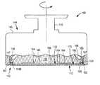
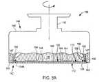
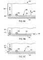
- FIGS. 3A and 3Beach illustrate a side view with a cut-away of the wafer carrier 106 of embodiments of the present invention in further detail.
- the wafer carrier 106comprises a carrier body 140 having a lower and upper end 142 and 144 .
- the lower end 142 of the carrier 106comprises a carrier base 146 , chuck, upon which the wafer 108 is held.
- the carrier basemay be made of variety of materials, such as plastic, steel or titanium.
- the carrier ring 147can have a surface portion that extends below the surface of the wafer that contacts the support pad 166 described further below.
- the carrier base 146is preferably surrounded by a carrier ring 147 .
- the carrier ringmay be constructed separately or may be an integral part of the carrier base.
- the carrier ringmay be made of plastic or any material that is stable in the process solutions.
- the wafer carrier 106is rotated or moved through the shaft 110 .
- a bottom surface 148 of the carrier base 146preferably disk shaped, includes a first surface portion 150 and a second surface portion 152 .
- the first surface portion 150is a peripheral surface surrounding the second surface portion 152 that is an inner region.
- the first and second surface portions 150 , 152 of the bottom surface 148are established by a sealing member 154 of the present invention, described hereinafter.
- the sealing member 154is placed into a circular groove 156 formed in the bottom surface 148 and between the first and second surfaces 150 , 152 defines an inner region of the base 146 , and, when the sealing member 154 contacts the back side of the wafer 108 , establishes a backside inner region of the wafer 108 .
- Fluid lines 158connect a fluid supply to a plurality of outlet ports 159 on the first surface portion 150 of the bottom surface 148 , as described further hereinafter.
- the outlet ports 159are radially distributed around the first surface 150 , such that the outlet ports are formed concentrically around the sealing member 154 .
- a lower end 160 of the fluid lines 158may run between the carrier base 146 and the carrier ring 147 .
- the fluid lines 158are used to blow a gas, preferably a non-oxidizing gas, onto a peripheral back edge 162 of the back surface 113 of the wafer 108 .
- the non-oxidizing gasmay preferably be nitrogen gas.
- Holesmay have any number and varied diameters, but preferably a diameter in the range of 0.5-1 mm found most preferable. In the preferred embodiment, at 16-64 holes are disposed around the edge of the wafer carrier, for wafer sizes of between 200 and 300 mm.
- the number of such holescan vary, and, instead of holes, a continuous slit or slits, or another shaped opening can be used instead.
- the gas flow ratecan vary, with a flow rate preferably between 10-60 liters per minute.
- the gas emitted from ports 159continuously sweeps the peripheral back edge 162 and provides another seal that assists in preventing liquid, such as electrolyte, from reaching behind the wafer 108 and causing unwanted contamination.
- the wafer 108is retained by the carrier base 146 by the application of vacuum suction.
- a number of vacuum lines 164are connected to the second surface 152 of the carrier base 146 .
- a support pad 166 or a backing padis preferably, but not necessarily, attached on the second surface portion 152 to maintain the wafer in a substantially flat state while under the applied vacuum suction.
- the vacuum lines 164continue through holes in the support pad 166 .
- the wafermay be held using a suction cup.
- the sealing member 154In order for the seal to be created, the sealing member 154 must extend past the support pad 166 , typically by an amount that is in the range of 50-100 microns, so that the seal can be properly formed. As described hereinafter, the sealing member 154 will be relatively much softer than the support pad 166 .
- the other componentssuch as mechanical components of the wafer carrier 106 may be conventionally constructed and well known in the art.
- the carrier head 106may be provided with some form of gimbal mechanism and cooperating mechanical components. Such conventional components need not be further described.
- the wafer 108is placed on the carrier base 146 as shown in FIGS. 3A and 3B, using a wafer handling system (not shown).
- the wafer 108is aligned with the sealing member 154 and under the applied vacuum, the sealing member 154 seals the space confined between the second surface portion 152 and the back 113 of the wafer, thereby retaining the wafer 108 on the wafer carrier 106 and fully exposing the front surface 112 of the wafer 108 .
- vacuum levels in the range of 400-650 Torrwere employed.
- the gas flow from the ports 159 , in the direction of the arrow 168sweeps away the electrolyte 120 flowing in the direction of the arrow 170 and assists in preventing the electrolyte solution from reaching the peripheral back edge 162 of the wafer 108 .
- the wafer carrier of the present inventionadvantageously prevents the electrolyte from reaching the back surface 113 of the wafer 108 while fully exposing the front surface 112 of the wafer to the processing solutions.
- the gascan be turned off so that it does not blow through the ports 159 , thereby allowing for access to the backside of the wafer 108 to a liquid cleaning solution, a gas fluid such as air, or both.
- the sealing member 154is designed such that the sealing function is efficiently achieved with the application of minimum vacuum suction.
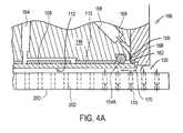
- the sealing member 154 A illustrated in FIGS. 3A and 4Ais an o-ring made of an insulating material.
- the o-ring 154 Amay or may not be hollow inside, but as shown in FIG. 4A, it will tend to retain its shape under pressure. It has been found that preferably the o-ring 154 A is hollow, having a diameter of 1-4 mm, and a thickness of between 0.5 and 1.5 mm.
- the hollow o-ringthere is softness to the hollow o-ring, such that it has a durometer rating of less than 70, and preferably within the range of 30-50 durometers, in contrast to typical o-rings that are much harder, and have a higher durometer rating, and support pads 166 that will have a durometer rating (which is a hardness rating) that typically are at least 5 times greater than that of the hollow o-ring.
- This softnessadvantageously allows for the desired seal to occur, without the detrimental side effect of causing bowing on the wafer due to the pressure of a hard seal exerting too much pressure onto the backside of the wafer.
- the o-ring 154 Aparticularly when hollow, is preferably made of an ethylene propylene material.
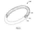
- the gasket 154 B illustrated in FIGS. 3B and 4Bis an alternative to the o-ring 154 A.
- the gasket 154 Bhas a circular body 300 having a bulb shape cross section.
- the body 300has a first portion 302 or an attachment portion and a second portion 304 or a sealing portion.
- the sealing portion 304may preferably be slanted outwardly to offer more sealing surface when the vacuum is applied, which will be described more fully below.
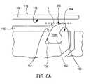
- FIG. 6Ashows the gasket 154 B in cross section and with no compressive force applied upon it or no wafer held on it.
- the gasket 154 Bis placed on the wafer carrier by inserting the attachment portion 302 into the circular groove 156 .
- the sealing portion 304 of the gasket 154 Bdefines a sealing surface 306 which is a slanted surface generally facing the back surface 113 of the wafer 108 .
- the sealing portion 304is a compression distance, denoted with ‘h’, higher than the top of the support pad 166 .
- the compression distancemay be in the range of 0.1 mm to 0.3 mm, preferably 0.2 mm. In sealing stage, the compression distance ‘h’ is reduced to zero, allowing full usage of the sealing surface 306 .
- FIG. 6Bshows the gasket 154 B when sealing the back surface 113 of the wafer 108 .
- the wafer 108presses against the sealing surface 306 and causes the sealing portion 304 to collapse thereby achieving sealing function.
- the gasket 154 Bachieves sealing function with ease, i.e., by the collapse of the sealing portion 306 and with providing larger sealing surface.
- the gasket 154 Bcan be made of an elastic material such as elastomer.
- an elastic materialsuch as elastomer.
- KalreZTMwhich can be available from DuPont. It is understood, however, that although in the preferred embodiment the gasket member of the present invention is described above, the gasket member may be made of any compressible material, membrane, or tube, or the like, as long as it performs the above given sealing functions, and is within the scope of the present invention.
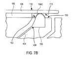
- a gasket member 154 Cmay be an inflatable membrane.
- FIG. 7Ashows the inflatable membrane in deflated stage.
- the inflatable membrane 154 Cis attached to and seals the perimeter edge of opening 402 of the circular grove 156 .
- the circular grooveis connected to a fluid line 404 through at least one inlet port 406 so that a fluid such as air can be used to inflate the inflatable membrane 154 C.
- the fluid line 404is further connected to a fluid supply system (not shown) such that the fluid pressure can be controlled.
- FIG. 7Bshows the inflatable member 154 C in inflated stage and when sealing the back surface 113 of the wafer 108 .
- the wafer 108presses against the inflatable membrane thereby achieving sealing function.
- the inflatable member 154 Cmay be made of any rubber or elastomer material.
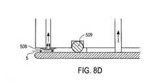
- FIGS. 8 A- 8 Dillustrate another embodiment of the present invention using a pair of concentric sealing members.
- a carrier head 500comprises a carrier body 502 and a carrier base 504 where a wafer or other workpiece 505 is held.
- the carrier head 500is rotated or moved through the shaft 508 .
- the carrier base 504comprises a bottom surface 506 that is preferably a surface that conforms to the shape of the workpiece, typically circular for a wafer.
- a first sealing member 508 and a second sealing member 509are concentrically placed adjacent outer circumference 510 of the bottom surface 506 .
- the first sealing member 508is preferably an inflatable gasket membrane having a circular strip shape.
- the membrane 508is attached to the bottom surface 506 of the carrier base 504 from its inner and outer circumferential edges 512 and 514 , respectively, such that an inner pocket 516 of the membrane 508 is formed.
- the inner pocket 516 of the membrane 508is connected to a fluid source (not shown), such as a gas source, through fluid lines 518 .
- a fluid sourcenot shown
- the fluid from the fluid lines 518is used to inflate the inflatable membrane 508 during the process.
- the second sealing member 509is preferably made such as one of the sealing members 154 described above. In a particularly preferred embodiment, the second sealing member is made as the hollow o-ring 154 A as described in FIGS.
- the second sealing member 509is preferably placed in a circular groove 520 .
- a support member 522may be concentrically placed within the circular area formed by the o-ring 509 .
- a number of vacuum lines 524are formed through the carrier base 504 and through the support member 522 so that when the wafer 505 is placed on the support member 522 , vacuum suction can be created on back side 526 of the wafer 505 , which is sealed by the second sealing member 509 .
- FIGS. 8 A- 8 Din operation, described in the preferred embodiment of the first sealing member 508 being an inflatable member and the second sealing member 509 being an o-ring, the back side 526 of the wafer 505 is placed on the o-ring 509 and vacuum suction is applied to hold the wafer 505 on the carrier 500 . It is understood that in this embodiment, front surface 528 of the wafer 505 is fully exposed. As shown in FIG. 8C, next the inflatable membrane 508 is inflated by supplying gas into the inner pocket 516 . In inflated state the inflatable membrane 509 effectively seals edge region 530 of the wafer 505 .
- both the inflatable membrane 508 and the o-ring 509form a double seal along the circumference/edge of the wafer 505 .
- Such combinationadvantageously prevents leakage of the process solutions, such as electrolyte, through both the inflatable member 508 , and the o-ring 509 and prevents contamination of the backside 526 of the wafer as well as of the support member 522 .
- this edge region 530can be easily cleaned, such as during a cleaning step after a plating step, as explained hereinafter.
- the first sealing member 508is preferably an inflatable member, since after a plating step in which both the first sealing member 508 , and the second sealing member 509 are providing a seal is completed, the first sealing member 508 , when an inflatable member, can be deflated, as shown, to expose a potentially contaminated edge region 530 while the wafer is still being held by the carrier 500 and the vacuum suction is still being applied to the area sealed by the o-ring 509 .
- cleaning of the edge region 530can occur by applying a cleaning fluid or fluids (such as either a liquid cleaning fluid, or both a liquid cleaning fluid and thereafter a gas such as air for drying) in the direction of arrow into the edge region 530 from a cleaning system (not shown) into the area that had previously been protected to the inflated inflatable member 508 .
- a cleaning fluid or fluidssuch as either a liquid cleaning fluid, or both a liquid cleaning fluid and thereafter a gas such as air for drying
- the carrier 500may also be spun.
- the first sealing member 508is preferably an inflatable membrane, for the reasons described above, other alternative seals, for example an o-ring, can also be used.
- FIGS. 9 A- 9 Cillustrate another embodiment of the present invention using a pair of concentric gasket members.
- This embodimentis similar to the FIG. 8 embodiment, as shown in the overview of FIG. 9A, in using a first seal member 908 and a concentric second seal member 909 to provide a seal for the backside of the wafer 905 within the interior region formed by the second seal member 909 , which interior region includes a support member 922 .
- the backside of the wafer 905is preferably held on the second sealing member 909 and the support member 922 through the usage of a vacuum that is applied through vacuum lines 924 .
- FIG. 9 A- 9 Cillustrate another embodiment of the present invention using a pair of concentric gasket members.
- This embodimentis similar to the FIG. 8 embodiment, as shown in the overview of FIG. 9A, in using a first seal member 908 and a concentric second seal member 909 to provide a seal for the backside of the wafer 905 within the interior region formed by the second seal member 909 ,
- the first sealing member 908is preferably an o-ring, which may or may not be hollow inside, but preferably has a softness that is softer than that of the second sealing member 909 .
- the seal with the first sealing member 908is also formed by having a vertically moveable annular housing 904 on the outside of the carrier head 900 .
- the vertical movabilitycan be achieved in a variety of manners, including a motorized sprocket along the inner radius of the annular housing 904 , other mechanical mechanisms, or otherwise.
- FIG. 9Billustrates in more detail the sealed position, in which both the first seal member 908 and the second seal member 909 provide the sealing function.
- the vertically moveable annular housing 904is moved downward, to establish the seal between the first sealing member 908 and the wafer 905 .
- the waferis processed in the chemical environment when both sealing members 908 and 909 seal the wafer 905 .
- the unsealed positionwhich allows a cleaning fluid, or gas, to be injected into the backside of the wafer outside of the second sealing member 909 , as shown by the arrows in FIG.
- the vertically moveable annular housingis moved upward, thereby disengaging the first sealing member 908 and providing a gap through which the cleaning fluid or gas can be injected to the peripheral backside of the wafer 905 , outside of the second sealing member 909 .
- eachis preferably coated with a material that allows for chemical compatibility with the process being performed, such as Teflon® for chemical compatibility with plating that uses an electrolyte as well as cleaning with conventional cleaning solutions.
Landscapes
- Engineering & Computer Science (AREA)
- Chemical & Material Sciences (AREA)
- Materials Engineering (AREA)
- Organic Chemistry (AREA)
- Metallurgy (AREA)
- Chemical Kinetics & Catalysis (AREA)
- Electrochemistry (AREA)
- Physics & Mathematics (AREA)
- Sustainable Development (AREA)
- Life Sciences & Earth Sciences (AREA)
- Mechanical Engineering (AREA)
- Condensed Matter Physics & Semiconductors (AREA)
- General Physics & Mathematics (AREA)
- Manufacturing & Machinery (AREA)
- Computer Hardware Design (AREA)
- Microelectronics & Electronic Packaging (AREA)
- Power Engineering (AREA)
- Container, Conveyance, Adherence, Positioning, Of Wafer (AREA)
- Cleaning Or Drying Semiconductors (AREA)
- Electroplating Methods And Accessories (AREA)
Abstract
Description
- This application is related to and claims priority from U.S. Provisional Application No. 60/275,406 filed on Mar. 12, 2001 and entitled Wafer Carrier For Wet Processes.[0001]
- 1. Field of the Invention[0002]
- The present invention generally relates to semiconductor processing technologies and, more particularly, to a versatile wafer carrier.[0003]
- 2. Description of the Related Art[0004]
- Conventional semiconductor devices generally include a semiconductor substrate, usually a silicon substrate, and a plurality of sequentially formed dielectric interlayers such as silicon dioxide and conductive paths or interconnects made of conductive materials. The interconnects are usually formed by filling a conductive material in trenches etched into the dielectric interlayers. In an integrated circuit, multiple levels of interconnect networks laterally extend with respect to the substrate surface. The interconnects formed in different layers can be electrically connected using vias or contacts. A conductive material filling process of such features, i.e., via openings, trenches, pads or contacts can be carried out by depositing a conductive material over the substrate including such features.[0005]
- Copper and copper alloys have recently received considerable attention as interconnect materials because of their superior electromigration and low resistivity characteristics. The preferred method of copper deposition is electrodeposition. During fabrication, copper or another conductive material is deposited on a substrate that has been previously coated with a conductor, typically a barrier layer and then a seed layer. Typical seed layers are made of copper and its alloys. Typical barrier materials generally include tungsten, tantalum, titanium, their alloys, and their nitrides. The deposition process can be carried out using a variety of processes.[0006]
- After depositing copper into the features on the semiconductor wafer surface, a removal process, such as an etching, an electro polishing or a chemical mechanical polishing (CMP) step, may be employed. Such removal processes remove the conductive materials off the surface of the wafer, particularly the field regions, thereby leaving the conductive materials primarily disposed within the features, such as vias, trenches and the like.[0007]
- During the deposition process or the removal process the wafer is generally held by a carrier head. As shown in FIG. 1A, a[0008]
conventional carrier head 10 having arotatable shaft 12 holds awafer 14 during the electrodeposition process. Thewafer 14 is placed on asurface 16 of a carrier base18 (chuck) of thecarrier head 10. During the deposition and/or material removal step, thecarrier head 10 secures thewafer 14 to thesurface 16 of thebase 18 of thecarrier head 10 by applying vacuum to the back of the wafer and usingclamps 20. The vacuum is applied usingvacuum lines 22 extending through thecarrier base 18 and the body of thecarrier head 10.Clamps 20 may also sealelectrical contacts 24 to thewafer 14. In such a conventional carrier head, because of the clamp around the periphery of the wafer, no deposition or material removal occurs at the edge of the wafer. - In use, the carrier head is immersed into a solution, typically an electrolyte in a deposition and certain material removal processes, or a slurry in a CMP material removal process, for example. During any such process, it is important to prevent leakage of the solution to the backside of the wafer. Such leakages to the backside of the wafer contaminate the wafer backside and the electrical contacts. Removal of contaminants from the wafer backside requires an extra process step that is time consuming and increases manufacturing cost.[0009]
- Another conventional wafer carrier design does not use vacuum suction on the back of the wafer to retain the wafer on the carrier and attempts to reduce contamination of the wafer backside and wafer edge during processing. Referring to FIG. 1B, with such a[0010]
wafer carrier 28, theback surface 30 of thewafer 32 is pressed against an o-ring 34 to form a seal between theback surface 30 of the wafer and the o-ring 34. Also, aclamp 36 including aseal 38 seals a perimeter of thefront surface 40 of thewafer 32 while housing the plurality ofcontacts 42 to thefront surface 40. In this prior art system, aregion 44 behind the seal can be pressurized with gas to further prevent contamination at the wafer backside. In such designs, because of the clamp around the periphery of the wafer, no deposition or material removal occurs at the edge of the wafer. - Yet another conventional CMP head is similar to the head shown in FIG. 1A, but it holds the wafer from the back side by vacuum and from the circumference of the wafer by a retaining ring, thereby fully exposing the front surface of the wafer. While the CMP process is done over the front surface of the wafer, the slurry from the CMP process can nevertheless migrate toward the back surface of the wafer.[0011]
- To this end, there is a need for a wafer carrier design that that may be used throughout either one or more process steps and be able to seal back of the wafer from the process solutions. There is also a need for a wafer carrier design that seals back of the wafer from the process solutions while exposing the entire front surface of the wafer for processing without excluding processing at the edge of the wafer.[0012]
- It is an object of the present invention to provide an improved wafer carrier.[0013]
- It is another object of the present invention to provide a wafer carrier that prevents processing liquids and contaminants resulting therefrom from reaching a backside inner region of the wafer.[0014]
- It is a further object of the present invention to provide a wafer carrier that prevents processing liquids and contaminants resulting therefrom from reaching an inner region of the base and a backside inner region of the wafer.[0015]
- The present invention attains the above objects, considered singly or in combination, among others, by providing a wafer carrier that includes an opening, which in one embodiment is a plurality of holes, disposed along the periphery of the wafer carrier. A gas emitted through the holes onto a peripheral back edge of the wafer assists in preventing the processing liquids and contaminants resulting therefrom from reaching the inner region of the base and the backside inner region of the wafer. In another embodiment, a plurality of concentric sealing members are used to prove a better seal, and the outer seal is preferably independently movable to allow cleaning of a peripheral backside of the wafer to occur while the wafer is still attached to the wafer carrier.[0016]
- Further, a sealing member, which are alternatively an o-ring, gasket, or inflatable member are used in specific embodiments to assist in preventing the processing liquids and contaminants resulting therefrom from reaching the backside inner region of the wafer.[0017]
- As noted in more detail below, the above-described characteristics of the wafer carrier can be used on different wafer carriers that are used in various processing environments.[0018]
- The above and other objectives, features, and advantages of the present invention are further described in the detailed description which follows, with reference to the drawings by way of non-limiting exemplary embodiments of the present invention, wherein like reference numerals represent similar parts of the present invention throughout several views and wherein:[0019]
- FIGS. 1A and 1B illustrate various conventional carrier heads;[0020]
- FIG. 2 illustrates an exemplary processing system on which carrier heads according to the present invention may be used.[0021]
- FIGS. 3A and 3B illustrate more detailed views of wafer carriers according to two embodiments of the present invention;[0022]
- FIGS. 4A and 4B illustrate injected gas and process fluid flow using the wafer carriers according the two embodiments illustrated in FIGS. 3A and 3B of the present invention;[0023]
- FIG. 5 illustrates a gasket member used in the embodiment of the present invention illustrated in FIGS. 3B and 4B;[0024]
- FIGS. 6A and 6B illustrate usage of the gasket member illustrated in FIG. 5 in more detail;[0025]
- FIGS. 7A and 7B illustrate another embodiment of a the present invention using an inflatable gasket member;[0026]
- FIGS.[0027]8A-8D illustrate another embodiment of the present invention using a pair of concentric gasket members; and
- FIGS.[0028]9A-9C illustrate another embodiment of the present invention using a pair of concentric gasket members.
- Reference will now be made to the drawings wherein like numerals refer to like parts throughout. As shown in FIG. 2, an[0029]
exemplary processing system 100. When used for electrodeposition, thesystem 100 may, for example, include acathode assembly 102 and ananode assembly 104 and can then deposit a conductive material such as copper on a workpiece or substrate, such as semiconductor wafer. When used for material removal, thesystem 100 may, for example, have the polarity of the anode and cathode reversed, or instead use other processing chemicals, such as a CMP slurry. It should be understood that the particular process in which the present invention is used is not of particular importance. What is significant, as illustrated hereinafter, is prevention of contamination of a processing solution from reaching a backside of a wafer. And in certain embodiments, also allowing for full face processing of the wafer to occur. - It should also be noted that in the description provided below in which copper is used as an example material that is deposited during a deposition process, other conductors can also be deposited during deposition processing, for example Ni, Pd, Pt, Au, Pb, Sn, Ag and their alloys.[0030]
- The[0031]
wafer holding assembly 102 of thesystem 100 includes awafer carrier 106, shown in FIG. 2 holding anexemplary wafer 108, which can be referred to as the cathode during deposition, the anode during electropolishing, or just the wafer if a process that does not require a current flow/voltage differential to exist. During deposition, for example, afront surface 112 of thewafer 108 is connected to a negative terminal of a power supply (not shown) byelectrical contact members 114. During electropolishing, for example, thefront surface 112 of thewafer 108 is connected to a positive terminal of a power supply (not shown) byelectrical contact members 114. - As will be described more fully below, the[0032]
wafer carrier 106 holds thewafer 108 from aback surface 113 of thewafer 108 using vacuum suction. In this embodiment, thewafer 108 is held by thewafer carrier 106 so that afront surface 112 of thewafer 108 is fully exposed. During the process, thewafer carrier 106 and hence thewafer 108 are moved by rotating acarrier shaft 110 about a rotation axis115 or vertical axis and/or by laterally translating thecarrier shaft 110. - The[0033]
electrode assembly 104 of thesystem 100 will typically have a different type ofelectrode 116, depending upon whetherassembly 104 is being used for deposition or electropolishing. When used for deposition, theelectrode 116 is an anode, preferably a consumable copper anode, and when used for electropolishing, theelectrode 116 is a cathode, and is preferably not consumable. Theelectrode 116 may preferably be placed into an enclosure such as anelectrode cup 118. Theelectrode 116 may have holes that allow the electrolyte to flow therethrough (not shown). Theelectrode cup 118 may have bleeding openings (not shown) to control the amount of the flow of solution, such as electrolyte when used for deposition and certain electropolishing techniques, or slurry if CMP is being used, for example. During processing, thesolution 120 is pumped into theelectrode cup 118 through aliquid inlet 130 to reach and wet thefront surface 112 of thewafer 108. Thesolution 120 flows in the direction of arrows and wets thefront surface 112 of thewafer 108. - During deposition or certain electropolishing processes, typically the[0034]
solution 120 is an electrolyte that is used to deposit material on thefront surface 112 of thewafer 108 under applied appropriate potential or remove material from thefront surface 112 of thewafer 108 under applied appropriate potential. During CMP, such potential may or may not be applied. With all processes, however, thewafer front surface 112 is preferably rotated as is known. - In the[0035]
system 100,electrical contact members 114contact wafer 108 on acontact region 126, as shown in FIG. 2. Thecontact region 126 is a peripheral ring region on the front surface of the wafer that has a portion thereof that is always exposed over the edge of theelectrode cup 118 as the wafer is rotated. - FIGS. 3A and 3B each illustrate a side view with a cut-away of the[0036]
wafer carrier 106 of embodiments of the present invention in further detail. As will become apparent, the difference between the embodiments illustrated in FIGS. 3A and 3B is the type of sealing member154 that is used. Thewafer carrier 106 comprises acarrier body 140 having a lower andupper end lower end 142 of thecarrier 106 comprises acarrier base 146, chuck, upon which thewafer 108 is held. The carrier base may be made of variety of materials, such as plastic, steel or titanium. And, as shown thecarrier ring 147 can have a surface portion that extends below the surface of the wafer that contacts thesupport pad 166 described further below. Thecarrier base 146 is preferably surrounded by acarrier ring 147. The carrier ring may be constructed separately or may be an integral part of the carrier base. The carrier ring may be made of plastic or any material that is stable in the process solutions. Thewafer carrier 106 is rotated or moved through theshaft 110. In this embodiment, abottom surface 148 of thecarrier base 146, preferably disk shaped, includes afirst surface portion 150 and asecond surface portion 152. Thefirst surface portion 150 is a peripheral surface surrounding thesecond surface portion 152 that is an inner region. The first andsecond surface portions bottom surface 148 are established by a sealing member154 of the present invention, described hereinafter. - The sealing member[0037]154 is placed into a
circular groove 156 formed in thebottom surface 148 and between the first andsecond surfaces base 146, and, when the sealing member154 contacts the back side of thewafer 108, establishes a backside inner region of thewafer 108.Fluid lines 158 connect a fluid supply to a plurality ofoutlet ports 159 on thefirst surface portion 150 of thebottom surface 148, as described further hereinafter. Theoutlet ports 159 are radially distributed around thefirst surface 150, such that the outlet ports are formed concentrically around the sealing member154. Although it may be directly connected to thefirst surface portion 150, alower end 160 of thefluid lines 158 may run between thecarrier base 146 and thecarrier ring 147. In these embodiments, thefluid lines 158 are used to blow a gas, preferably a non-oxidizing gas, onto a peripheralback edge 162 of theback surface 113 of thewafer 108. The non-oxidizing gas may preferably be nitrogen gas. Holes may have any number and varied diameters, but preferably a diameter in the range of 0.5-1 mm found most preferable. In the preferred embodiment, at 16-64 holes are disposed around the edge of the wafer carrier, for wafer sizes of between 200 and 300 mm. Of course, the number of such holes can vary, and, instead of holes, a continuous slit or slits, or another shaped opening can be used instead. The gas flow rate can vary, with a flow rate preferably between 10-60 liters per minute. As will be described more fully below, the gas emitted fromports 159 continuously sweeps theperipheral back edge 162 and provides another seal that assists in preventing liquid, such as electrolyte, from reaching behind thewafer 108 and causing unwanted contamination. - The[0038]
wafer 108 is retained by thecarrier base 146 by the application of vacuum suction. For this purpose, a number ofvacuum lines 164 are connected to thesecond surface 152 of thecarrier base 146. In order to support the back surface of the wafer, asupport pad 166 or a backing pad is preferably, but not necessarily, attached on thesecond surface portion 152 to maintain the wafer in a substantially flat state while under the applied vacuum suction. When asupport pad 166 is used, thevacuum lines 164 continue through holes in thesupport pad 166. Although in this embodiment the wafer is held by vacuum applied through thelines 164, the wafer may be held using a suction cup. In order for the seal to be created, the sealing member154 must extend past thesupport pad 166, typically by an amount that is in the range of 50-100 microns, so that the seal can be properly formed. As described hereinafter, the sealing member154 will be relatively much softer than thesupport pad 166. - The other components, such as mechanical components of the[0039]
wafer carrier 106 may be conventionally constructed and well known in the art. Thecarrier head 106 may be provided with some form of gimbal mechanism and cooperating mechanical components. Such conventional components need not be further described. - In use, the[0040]
wafer 108 is placed on thecarrier base 146 as shown in FIGS. 3A and 3B, using a wafer handling system (not shown). Thewafer 108 is aligned with the sealing member154 and under the applied vacuum, the sealing member154 seals the space confined between thesecond surface portion 152 and the back113 of the wafer, thereby retaining thewafer 108 on thewafer carrier 106 and fully exposing thefront surface 112 of thewafer 108. In the preferred embodiment, vacuum levels in the range of 400-650 Torr were employed. - Once the[0041]
wafer 108 is held by thecarrier 106, gas is blown through theports 159 onto theperipheral back edge 162 as the wafer is processed during deposition, in an amount as described above. - As shown in FIGS. 4A and 4B, during the above exemplified deposition process, the gas flow from the[0042]
ports 159, in the direction of thearrow 168, sweeps away theelectrolyte 120 flowing in the direction of thearrow 170 and assists in preventing the electrolyte solution from reaching theperipheral back edge 162 of thewafer 108. In cooperation with the sealing member154, the wafer carrier of the present invention advantageously prevents the electrolyte from reaching theback surface 113 of thewafer 108 while fully exposing thefront surface 112 of the wafer to the processing solutions. - During a subsequent cleaning step, however, the gas can be turned off so that it does not blow through the[0043]
ports 159, thereby allowing for access to the backside of thewafer 108 to a liquid cleaning solution, a gas fluid such as air, or both. - In accordance with the principles of the present invention, the sealing member[0044]154 is designed such that the sealing function is efficiently achieved with the application of minimum vacuum suction.
- The sealing[0045]
member 154A illustrated in FIGS. 3A and 4A is an o-ring made of an insulating material. The o-ring 154A may or may not be hollow inside, but as shown in FIG. 4A, it will tend to retain its shape under pressure. It has been found that preferably the o-ring 154A is hollow, having a diameter of 1-4 mm, and a thickness of between 0.5 and 1.5 mm. Put in other terms, there is softness to the hollow o-ring, such that it has a durometer rating of less than 70, and preferably within the range of 30-50 durometers, in contrast to typical o-rings that are much harder, and have a higher durometer rating, andsupport pads 166 that will have a durometer rating (which is a hardness rating) that typically are at least 5 times greater than that of the hollow o-ring. This softness advantageously allows for the desired seal to occur, without the detrimental side effect of causing bowing on the wafer due to the pressure of a hard seal exerting too much pressure onto the backside of the wafer. The o-ring 154A, particularly when hollow, is preferably made of an ethylene propylene material. - The[0046]
gasket 154B illustrated in FIGS. 3B and 4B is an alternative to the o-ring 154A. As shown in FIG. 5 in partial perspective view, thegasket 154B has acircular body 300 having a bulb shape cross section. Thebody 300 has afirst portion 302 or an attachment portion and asecond portion 304 or a sealing portion. The sealingportion 304 may preferably be slanted outwardly to offer more sealing surface when the vacuum is applied, which will be described more fully below. - FIG. 6A shows the[0047]
gasket 154B in cross section and with no compressive force applied upon it or no wafer held on it. Referring to FIG. 6A, thegasket 154B is placed on the wafer carrier by inserting theattachment portion 302 into thecircular groove 156. The sealingportion 304 of thegasket 154B defines a sealingsurface 306 which is a slanted surface generally facing theback surface 113 of thewafer 108. The sealingportion 304 is a compression distance, denoted with ‘h’, higher than the top of thesupport pad 166. The compression distance may be in the range of 0.1 mm to 0.3 mm, preferably 0.2 mm. In sealing stage, the compression distance ‘h’ is reduced to zero, allowing full usage of the sealingsurface 306. - FIG. 6B shows the[0048]
gasket 154B when sealing theback surface 113 of thewafer 108. As illustrated in FIG. 6B, as vacuum suction is applied to theback surface 113 of thewafer 108, thewafer 108 presses against the sealingsurface 306 and causes the sealingportion 304 to collapse thereby achieving sealing function. Thegasket 154B achieves sealing function with ease, i.e., by the collapse of the sealingportion 306 and with providing larger sealing surface. - In this embodiment, the[0049]
gasket 154B can be made of an elastic material such as elastomer. One such material is commercially available under the brand name KalreZ™, which can be available from DuPont. It is understood, however, that although in the preferred embodiment the gasket member of the present invention is described above, the gasket member may be made of any compressible material, membrane, or tube, or the like, as long as it performs the above given sealing functions, and is within the scope of the present invention. - As shown in FIG. 7A, in an alternative embodiment, a[0050]
gasket member 154C may be an inflatable membrane. FIG. 7A shows the inflatable membrane in deflated stage. Theinflatable membrane 154C is attached to and seals the perimeter edge of opening402 of thecircular grove 156. In this embodiment the circular groove is connected to afluid line 404 through at least oneinlet port 406 so that a fluid such as air can be used to inflate theinflatable membrane 154C. Thefluid line 404 is further connected to a fluid supply system (not shown) such that the fluid pressure can be controlled. - FIG. 7B shows the[0051]
inflatable member 154C in inflated stage and when sealing theback surface 113 of thewafer 108. As vacuum suction is applied, thewafer 108 presses against the inflatable membrane thereby achieving sealing function. By controlling the fluid pressure, the force applied by themember 154C to the back of thewafer 108 may be optimized. This, in turn, provides efficient sealing without causing the above explained prior art wafer sinking problem. Theinflatable member 154C may be made of any rubber or elastomer material. - It is also noted that it is within the scope of the present invention, as described above with reference to FIGS.[0052]3A-7B to use any of the sealing members154 as described injecting gas through the
ports 159. - FIGS.[0053]8A-8D illustrate another embodiment of the present invention using a pair of concentric sealing members. In this embodiment, as illustrated, a
carrier head 500 comprises acarrier body 502 and acarrier base 504 where a wafer orother workpiece 505 is held. Thecarrier head 500 is rotated or moved through theshaft 508. Thecarrier base 504 comprises abottom surface 506 that is preferably a surface that conforms to the shape of the workpiece, typically circular for a wafer. Afirst sealing member 508 and asecond sealing member 509 are concentrically placed adjacentouter circumference 510 of thebottom surface 506. - The[0054]
first sealing member 508 is preferably an inflatable gasket membrane having a circular strip shape. Themembrane 508 is attached to thebottom surface 506 of thecarrier base 504 from its inner and outercircumferential edges inner pocket 516 of themembrane 508 is formed. Theinner pocket 516 of themembrane 508 is connected to a fluid source (not shown), such as a gas source, throughfluid lines 518. As will be described below, the fluid from thefluid lines 518 is used to inflate theinflatable membrane 508 during the process. Thesecond sealing member 509 is preferably made such as one of the sealing members154 described above. In a particularly preferred embodiment, the second sealing member is made as the hollow o-ring 154A as described in FIGS. 3A and 4A. Thesecond sealing member 509 is preferably placed in acircular groove 520. Asupport member 522 may be concentrically placed within the circular area formed by the o-ring 509. A number ofvacuum lines 524 are formed through thecarrier base 504 and through thesupport member 522 so that when thewafer 505 is placed on thesupport member 522, vacuum suction can be created onback side 526 of thewafer 505, which is sealed by thesecond sealing member 509. - As shown in FIGS.[0055]8A-8D, in operation, described in the preferred embodiment of the
first sealing member 508 being an inflatable member and thesecond sealing member 509 being an o-ring, theback side 526 of thewafer 505 is placed on the o-ring 509 and vacuum suction is applied to hold thewafer 505 on thecarrier 500. It is understood that in this embodiment, front surface528 of thewafer 505 is fully exposed. As shown in FIG. 8C, next theinflatable membrane 508 is inflated by supplying gas into theinner pocket 516. In inflated state theinflatable membrane 509 effectively sealsedge region 530 of thewafer 505. In this respect, the combination of both theinflatable membrane 508 and the o-ring 509 form a double seal along the circumference/edge of thewafer 505. Such combination advantageously prevents leakage of the process solutions, such as electrolyte, through both theinflatable member 508, and the o-ring 509 and prevents contamination of thebackside 526 of the wafer as well as of thesupport member 522. And, even if there is some leakage within theinflatable member 508 of the process solution into theedge region 530 that exists between theinflatable member 508 and the o-ring 509, thisedge region 530 can be easily cleaned, such as during a cleaning step after a plating step, as explained hereinafter. - As shown in FIG. 8D, it becomes apparent why the[0056]
first sealing member 508 is preferably an inflatable member, since after a plating step in which both thefirst sealing member 508, and thesecond sealing member 509 are providing a seal is completed, thefirst sealing member 508, when an inflatable member, can be deflated, as shown, to expose a potentially contaminatededge region 530 while the wafer is still being held by thecarrier 500 and the vacuum suction is still being applied to the area sealed by the o-ring 509. Thus, in this configuration, cleaning of theedge region 530 can occur by applying a cleaning fluid or fluids (such as either a liquid cleaning fluid, or both a liquid cleaning fluid and thereafter a gas such as air for drying) in the direction of arrow into theedge region 530 from a cleaning system (not shown) into the area that had previously been protected to the inflatedinflatable member 508. During the cleaning and a subsequent drying step thecarrier 500 may also be spun. Although in this embodiment thefirst sealing member 508 is preferably an inflatable membrane, for the reasons described above, other alternative seals, for example an o-ring, can also be used. - FIGS.[0057]9A-9C illustrate another embodiment of the present invention using a pair of concentric gasket members. This embodiment is similar to the FIG. 8 embodiment, as shown in the overview of FIG. 9A, in using a
first seal member 908 and a concentricsecond seal member 909 to provide a seal for the backside of thewafer 905 within the interior region formed by thesecond seal member 909, which interior region includes asupport member 922. As in the previous embodiments the backside of thewafer 905 is preferably held on thesecond sealing member 909 and thesupport member 922 through the usage of a vacuum that is applied throughvacuum lines 924. In contrast to the FIG. 8 embodiment, however, instead of having an inflatable first sealing member, thefirst sealing member 908 is preferably an o-ring, which may or may not be hollow inside, but preferably has a softness that is softer than that of thesecond sealing member 909. The seal with thefirst sealing member 908 is also formed by having a vertically moveableannular housing 904 on the outside of thecarrier head 900. The vertical movability can be achieved in a variety of manners, including a motorized sprocket along the inner radius of theannular housing 904, other mechanical mechanisms, or otherwise. - FIG. 9B illustrates in more detail the sealed position, in which both the[0058]
first seal member 908 and thesecond seal member 909 provide the sealing function. In this sealed position, the vertically moveableannular housing 904 is moved downward, to establish the seal between thefirst sealing member 908 and thewafer 905. The wafer is processed in the chemical environment when both sealingmembers wafer 905. In the unsealed position, which allows a cleaning fluid, or gas, to be injected into the backside of the wafer outside of thesecond sealing member 909, as shown by the arrows in FIG. 9C, the vertically moveable annular housing is moved upward, thereby disengaging thefirst sealing member 908 and providing a gap through which the cleaning fluid or gas can be injected to the peripheral backside of thewafer 905, outside of thesecond sealing member 909. - With respect to the various sealing members described herein, it is further noted that each is preferably coated with a material that allows for chemical compatibility with the process being performed, such as Teflon® for chemical compatibility with plating that uses an electrolyte as well as cleaning with conventional cleaning solutions.[0059]
- Although various preferred embodiments have been described in detail above, those skilled in the art will readily appreciate that many modifications of the exemplary embodiment are possible without materially departing from the novel teachings and advantages of this invention. For example, although an o-ring, gasket, and inflatable member are described to provide the vacuum seal, any material or device that may provide this sealing may replace o-ring and be within the scope of this invention. It will thus be appreciated that in some instances some features of the invention will be employed without a corresponding use of other features without departing from the spirit and scope of the invention as set forth in the appended claims.[0060]
Claims (38)
Priority Applications (1)
| Application Number | Priority Date | Filing Date | Title |
|---|---|---|---|
| US10/788,926US6988932B2 (en) | 2001-03-12 | 2004-02-25 | Apparatus of sealing wafer backside for full-face processing |
Applications Claiming Priority (3)
| Application Number | Priority Date | Filing Date | Title |
|---|---|---|---|
| US27540601P | 2001-03-12 | 2001-03-12 | |
| US09/910,686US6855037B2 (en) | 2001-03-12 | 2001-07-20 | Method of sealing wafer backside for full-face electrochemical plating |
| US10/788,926US6988932B2 (en) | 2001-03-12 | 2004-02-25 | Apparatus of sealing wafer backside for full-face processing |
Related Parent Applications (1)
| Application Number | Title | Priority Date | Filing Date |
|---|---|---|---|
| US09/910,686ContinuationUS6855037B2 (en) | 2001-03-12 | 2001-07-20 | Method of sealing wafer backside for full-face electrochemical plating |
Publications (2)
| Publication Number | Publication Date |
|---|---|
| US20040166789A1true US20040166789A1 (en) | 2004-08-26 |
| US6988932B2 US6988932B2 (en) | 2006-01-24 |
Family
ID=26957400
Family Applications (2)
| Application Number | Title | Priority Date | Filing Date |
|---|---|---|---|
| US09/910,686Expired - Fee RelatedUS6855037B2 (en) | 2001-03-12 | 2001-07-20 | Method of sealing wafer backside for full-face electrochemical plating |
| US10/788,926Expired - Fee RelatedUS6988932B2 (en) | 2001-03-12 | 2004-02-25 | Apparatus of sealing wafer backside for full-face processing |
Family Applications Before (1)
| Application Number | Title | Priority Date | Filing Date |
|---|---|---|---|
| US09/910,686Expired - Fee RelatedUS6855037B2 (en) | 2001-03-12 | 2001-07-20 | Method of sealing wafer backside for full-face electrochemical plating |
Country Status (5)
| Country | Link |
|---|---|
| US (2) | US6855037B2 (en) |
| EP (1) | EP1390967A2 (en) |
| JP (1) | JP2005501395A (en) |
| TW (1) | TW550675B (en) |
| WO (1) | WO2002075792A2 (en) |
Cited By (10)
| Publication number | Priority date | Publication date | Assignee | Title |
|---|---|---|---|---|
| US20040009738A1 (en)* | 2002-05-17 | 2004-01-15 | Tokyo Seimitsu Co., Ltd. | Method and apparatus for chemical and mechanical polishing |
| US20070051393A1 (en)* | 2005-09-07 | 2007-03-08 | Samsung Electronics Co., Ltd. | Apparatus for cleaning a wafer |
| US20070151673A1 (en)* | 2005-12-29 | 2007-07-05 | Lg.Philips Lcd Co., Ltd. | Substrate bonding apparatus for liquid crystal display panel |
| US20100083969A1 (en)* | 2005-06-16 | 2010-04-08 | Geoffrey Crumblin | Swivel elbow for mask assembly |
| WO2018071402A1 (en)* | 2016-10-11 | 2018-04-19 | Veeco Instruments Inc. | Seal for wafer processing assembly |
| WO2019023636A1 (en)* | 2017-07-28 | 2019-01-31 | Tokyo Electron Limited | System and method for backside deposition of a substrate |
| US20210020492A1 (en)* | 2019-07-18 | 2021-01-21 | Taiwan Semiconductor Manufacturing Company, Ltd. | Chuck Design and Method for Wafer |
| WO2021221872A1 (en)* | 2020-04-30 | 2021-11-04 | Lam Research Corporation | Lipseal edge exclusion engineering to maintain material integrity at wafer edge |
| EP4227738A1 (en) | 2022-02-14 | 2023-08-16 | ASML Netherlands B.V. | Clamp |
| US12241173B2 (en) | 2019-10-04 | 2025-03-04 | Lam Research Corporation | Wafer shielding for prevention of lipseal plate-out |
Families Citing this family (266)
| Publication number | Priority date | Publication date | Assignee | Title |
|---|---|---|---|---|
| US8475636B2 (en) | 2008-11-07 | 2013-07-02 | Novellus Systems, Inc. | Method and apparatus for electroplating |
| US6939206B2 (en)* | 2001-03-12 | 2005-09-06 | Asm Nutool, Inc. | Method and apparatus of sealing wafer backside for full-face electrochemical plating |
| KR100993916B1 (en)* | 2002-06-06 | 2010-11-11 | 가부시키가이샤 에바라 세이사꾸쇼 | Substrate Processing Apparatus and Substrate Processing Method |
| EP1577421A1 (en)* | 2002-11-15 | 2005-09-21 | Ebara Corporation | Substrate processing apparatus and method for processing substrate |
| US7205960B2 (en) | 2003-02-19 | 2007-04-17 | Mirage Innovations Ltd. | Chromatic planar optic display system |
| US7063604B2 (en)* | 2004-03-05 | 2006-06-20 | Strasbaugh | Independent edge control for CMP carriers |
| US7573640B2 (en)* | 2005-04-04 | 2009-08-11 | Mirage Innovations Ltd. | Multi-plane optical apparatus |
| US20070026772A1 (en)* | 2005-07-28 | 2007-02-01 | Dolechek Kert L | Apparatus for use in processing a semiconductor workpiece |
| EP1942364A1 (en) | 2005-09-14 | 2008-07-09 | Mirage Innovations Ltd. | Diffractive optical relay and method for manufacturing the same |
| WO2007031992A1 (en)* | 2005-09-14 | 2007-03-22 | Mirage Innovations Ltd. | Diffraction grating with a spatially varying duty-cycle |
| EP1943556B1 (en)* | 2005-11-03 | 2009-02-11 | Mirage Innovations Ltd. | Binocular optical relay device |
| SE529882C2 (en)* | 2006-03-24 | 2007-12-18 | Swedish Electroforming Technol | Apparatus and method for fixing a matrix plate during electroplating |
| JP4642787B2 (en)* | 2006-05-09 | 2011-03-02 | 東京エレクトロン株式会社 | Substrate transfer device and vertical heat treatment device |
| US9822461B2 (en) | 2006-08-16 | 2017-11-21 | Novellus Systems, Inc. | Dynamic current distribution control apparatus and method for wafer electroplating |
| WO2008023375A1 (en)* | 2006-08-23 | 2008-02-28 | Mirage Innovations Ltd. | Diffractive optical relay device with improved color uniformity |
| JP5157199B2 (en)* | 2007-03-07 | 2013-03-06 | 東京エレクトロン株式会社 | Vacuum vessel, pressure vessel and sealing method thereof |
| US20100302644A1 (en)* | 2007-09-18 | 2010-12-02 | Mirage Innovations Ltd | Slanted optical device |
| US8858774B2 (en) | 2008-11-07 | 2014-10-14 | Novellus Systems, Inc. | Electroplating apparatus for tailored uniformity profile |
| DE202009018907U1 (en)* | 2009-08-12 | 2014-05-15 | Satisloh Ag | Flexible polishing tool for fine machining of optically effective surfaces on in particular spectacle lenses |
| WO2012007521A1 (en)* | 2010-07-15 | 2012-01-19 | Replisaurus Group Sas | A contact sheet for arrangement between a chuck and a master electrode in an ecpr process |
| JP5648954B2 (en)* | 2010-08-31 | 2015-01-07 | 不二越機械工業株式会社 | Polishing equipment |
| US8939815B2 (en)* | 2011-02-21 | 2015-01-27 | Taiwan Semiconductor Manufacturing Company, Ltd. | Systems providing an air zone for a chucking stage |
| US20130023129A1 (en) | 2011-07-20 | 2013-01-24 | Asm America, Inc. | Pressure transmitter for a semiconductor processing environment |
| JP5841798B2 (en)* | 2011-10-12 | 2016-01-13 | 株式会社ディスコ | Grinding equipment |
| JP2014072510A (en)* | 2012-10-02 | 2014-04-21 | Disco Abrasive Syst Ltd | Chuck table |
| US9909228B2 (en) | 2012-11-27 | 2018-03-06 | Lam Research Corporation | Method and apparatus for dynamic current distribution control during electroplating |
| US9583363B2 (en) | 2012-12-31 | 2017-02-28 | Sunedison Semiconductor Limited (Uen201334164H) | Processes and apparatus for preparing heterostructures with reduced strain by radial distension |
| US20160376700A1 (en) | 2013-02-01 | 2016-12-29 | Asm Ip Holding B.V. | System for treatment of deposition reactor |
| JP2015109416A (en)* | 2013-10-21 | 2015-06-11 | 東芝機械株式会社 | Chuck device |
| US10941490B2 (en) | 2014-10-07 | 2021-03-09 | Asm Ip Holding B.V. | Multiple temperature range susceptor, assembly, reactor and system including the susceptor, and methods of using the same |
| US9752248B2 (en) | 2014-12-19 | 2017-09-05 | Lam Research Corporation | Methods and apparatuses for dynamically tunable wafer-edge electroplating |
| US9567685B2 (en) | 2015-01-22 | 2017-02-14 | Lam Research Corporation | Apparatus and method for dynamic control of plated uniformity with the use of remote electric current |
| US10276355B2 (en) | 2015-03-12 | 2019-04-30 | Asm Ip Holding B.V. | Multi-zone reactor, system including the reactor, and method of using the same |
| US20170053822A1 (en)* | 2015-08-23 | 2017-02-23 | Camtek Ltd. | Warped wafers vacuum chuck |
| US9864283B2 (en)* | 2015-11-18 | 2018-01-09 | Applied Materials, Inc. | Apparatus and methods for photomask backside cleaning |
| US11139308B2 (en) | 2015-12-29 | 2021-10-05 | Asm Ip Holding B.V. | Atomic layer deposition of III-V compounds to form V-NAND devices |
| US10529554B2 (en) | 2016-02-19 | 2020-01-07 | Asm Ip Holding B.V. | Method for forming silicon nitride film selectively on sidewalls or flat surfaces of trenches |
| JP6546550B2 (en) | 2016-03-09 | 2019-07-17 | 日本特殊陶業株式会社 | Vacuum adsorption member and vacuum adsorption method |
| US10343920B2 (en) | 2016-03-18 | 2019-07-09 | Asm Ip Holding B.V. | Aligned carbon nanotubes |
| US11453943B2 (en) | 2016-05-25 | 2022-09-27 | Asm Ip Holding B.V. | Method for forming carbon-containing silicon/metal oxide or nitride film by ALD using silicon precursor and hydrocarbon precursor |
| US10612137B2 (en) | 2016-07-08 | 2020-04-07 | Asm Ip Holdings B.V. | Organic reactants for atomic layer deposition |
| US9859151B1 (en) | 2016-07-08 | 2018-01-02 | Asm Ip Holding B.V. | Selective film deposition method to form air gaps |
| US9812320B1 (en) | 2016-07-28 | 2017-11-07 | Asm Ip Holding B.V. | Method and apparatus for filling a gap |
| US9887082B1 (en) | 2016-07-28 | 2018-02-06 | Asm Ip Holding B.V. | Method and apparatus for filling a gap |
| US11532757B2 (en) | 2016-10-27 | 2022-12-20 | Asm Ip Holding B.V. | Deposition of charge trapping layers |
| US10714350B2 (en) | 2016-11-01 | 2020-07-14 | ASM IP Holdings, B.V. | Methods for forming a transition metal niobium nitride film on a substrate by atomic layer deposition and related semiconductor device structures |
| KR102546317B1 (en) | 2016-11-15 | 2023-06-21 | 에이에스엠 아이피 홀딩 비.브이. | Gas supply unit and substrate processing apparatus including the same |
| NL2017806B1 (en)* | 2016-11-16 | 2018-05-25 | Suess Microtec Photomask Equipment Gmbh & Co Kg | Holder for receiving and protecting one side of a photomask or of a photomask with pellicle from a cleaning medium, method for cleaning a photomask or a photomask with pellicle and apparatus for opening and closing a holder |
| US11447861B2 (en) | 2016-12-15 | 2022-09-20 | Asm Ip Holding B.V. | Sequential infiltration synthesis apparatus and a method of forming a patterned structure |
| US11581186B2 (en) | 2016-12-15 | 2023-02-14 | Asm Ip Holding B.V. | Sequential infiltration synthesis apparatus |
| US11390950B2 (en) | 2017-01-10 | 2022-07-19 | Asm Ip Holding B.V. | Reactor system and method to reduce residue buildup during a film deposition process |
| US10468261B2 (en) | 2017-02-15 | 2019-11-05 | Asm Ip Holding B.V. | Methods for forming a metallic film on a substrate by cyclical deposition and related semiconductor device structures |
| US10770286B2 (en) | 2017-05-08 | 2020-09-08 | Asm Ip Holdings B.V. | Methods for selectively forming a silicon nitride film on a substrate and related semiconductor device structures |
| US12040200B2 (en) | 2017-06-20 | 2024-07-16 | Asm Ip Holding B.V. | Semiconductor processing apparatus and methods for calibrating a semiconductor processing apparatus |
| US11306395B2 (en) | 2017-06-28 | 2022-04-19 | Asm Ip Holding B.V. | Methods for depositing a transition metal nitride film on a substrate by atomic layer deposition and related deposition apparatus |
| KR20190009245A (en) | 2017-07-18 | 2019-01-28 | 에이에스엠 아이피 홀딩 비.브이. | Methods for forming a semiconductor device structure and related semiconductor device structures |
| US11374112B2 (en) | 2017-07-19 | 2022-06-28 | Asm Ip Holding B.V. | Method for depositing a group IV semiconductor and related semiconductor device structures |
| US10590535B2 (en) | 2017-07-26 | 2020-03-17 | Asm Ip Holdings B.V. | Chemical treatment, deposition and/or infiltration apparatus and method for using the same |
| TWI815813B (en) | 2017-08-04 | 2023-09-21 | 荷蘭商Asm智慧財產控股公司 | Showerhead assembly for distributing a gas within a reaction chamber |
| US10692741B2 (en) | 2017-08-08 | 2020-06-23 | Asm Ip Holdings B.V. | Radiation shield |
| US10770336B2 (en) | 2017-08-08 | 2020-09-08 | Asm Ip Holding B.V. | Substrate lift mechanism and reactor including same |
| US11769682B2 (en) | 2017-08-09 | 2023-09-26 | Asm Ip Holding B.V. | Storage apparatus for storing cassettes for substrates and processing apparatus equipped therewith |
| JP2019039446A (en)* | 2017-08-22 | 2019-03-14 | 株式会社バルカー | Seal structure |
| US11830730B2 (en) | 2017-08-29 | 2023-11-28 | Asm Ip Holding B.V. | Layer forming method and apparatus |
| US11295980B2 (en) | 2017-08-30 | 2022-04-05 | Asm Ip Holding B.V. | Methods for depositing a molybdenum metal film over a dielectric surface of a substrate by a cyclical deposition process and related semiconductor device structures |
| US10658205B2 (en) | 2017-09-28 | 2020-05-19 | Asm Ip Holdings B.V. | Chemical dispensing apparatus and methods for dispensing a chemical to a reaction chamber |
| US10403504B2 (en) | 2017-10-05 | 2019-09-03 | Asm Ip Holding B.V. | Method for selectively depositing a metallic film on a substrate |
| US10923344B2 (en) | 2017-10-30 | 2021-02-16 | Asm Ip Holding B.V. | Methods for forming a semiconductor structure and related semiconductor structures |
| WO2019103613A1 (en) | 2017-11-27 | 2019-05-31 | Asm Ip Holding B.V. | A storage device for storing wafer cassettes for use with a batch furnace |
| CN111344522B (en) | 2017-11-27 | 2022-04-12 | 阿斯莫Ip控股公司 | Including clean mini-environment device |
| US10872771B2 (en) | 2018-01-16 | 2020-12-22 | Asm Ip Holding B. V. | Method for depositing a material film on a substrate within a reaction chamber by a cyclical deposition process and related device structures |
| TWI799494B (en) | 2018-01-19 | 2023-04-21 | 荷蘭商Asm 智慧財產控股公司 | Deposition method |
| KR102695659B1 (en) | 2018-01-19 | 2024-08-14 | 에이에스엠 아이피 홀딩 비.브이. | Method for depositing a gap filling layer by plasma assisted deposition |
| US11081345B2 (en) | 2018-02-06 | 2021-08-03 | Asm Ip Holding B.V. | Method of post-deposition treatment for silicon oxide film |
| US10896820B2 (en) | 2018-02-14 | 2021-01-19 | Asm Ip Holding B.V. | Method for depositing a ruthenium-containing film on a substrate by a cyclical deposition process |
| WO2019158960A1 (en) | 2018-02-14 | 2019-08-22 | Asm Ip Holding B.V. | A method for depositing a ruthenium-containing film on a substrate by a cyclical deposition process |
| US10731249B2 (en) | 2018-02-15 | 2020-08-04 | Asm Ip Holding B.V. | Method of forming a transition metal containing film on a substrate by a cyclical deposition process, a method for supplying a transition metal halide compound to a reaction chamber, and related vapor deposition apparatus |
| KR102636427B1 (en) | 2018-02-20 | 2024-02-13 | 에이에스엠 아이피 홀딩 비.브이. | Substrate processing method and apparatus |
| US10975470B2 (en) | 2018-02-23 | 2021-04-13 | Asm Ip Holding B.V. | Apparatus for detecting or monitoring for a chemical precursor in a high temperature environment |
| US11473195B2 (en) | 2018-03-01 | 2022-10-18 | Asm Ip Holding B.V. | Semiconductor processing apparatus and a method for processing a substrate |
| KR102646467B1 (en) | 2018-03-27 | 2024-03-11 | 에이에스엠 아이피 홀딩 비.브이. | Method of forming an electrode on a substrate and a semiconductor device structure including an electrode |
| KR102600229B1 (en) | 2018-04-09 | 2023-11-10 | 에이에스엠 아이피 홀딩 비.브이. | Substrate supporting device, substrate processing apparatus including the same and substrate processing method |
| US12025484B2 (en) | 2018-05-08 | 2024-07-02 | Asm Ip Holding B.V. | Thin film forming method |
| US12272527B2 (en) | 2018-05-09 | 2025-04-08 | Asm Ip Holding B.V. | Apparatus for use with hydrogen radicals and method of using same |
| DE102018111858A1 (en) | 2018-05-17 | 2019-11-21 | Nexwafe Gmbh | Device and method for one-sided etching of a semiconductor layer of a workpiece |
| KR102596988B1 (en) | 2018-05-28 | 2023-10-31 | 에이에스엠 아이피 홀딩 비.브이. | Method of processing a substrate and a device manufactured by the same |
| US11718913B2 (en) | 2018-06-04 | 2023-08-08 | Asm Ip Holding B.V. | Gas distribution system and reactor system including same |
| US10797133B2 (en) | 2018-06-21 | 2020-10-06 | Asm Ip Holding B.V. | Method for depositing a phosphorus doped silicon arsenide film and related semiconductor device structures |
| KR102568797B1 (en) | 2018-06-21 | 2023-08-21 | 에이에스엠 아이피 홀딩 비.브이. | Substrate processing system |
| KR102854019B1 (en) | 2018-06-27 | 2025-09-02 | 에이에스엠 아이피 홀딩 비.브이. | Periodic deposition method for forming a metal-containing material and films and structures comprising the metal-containing material |
| TWI873894B (en) | 2018-06-27 | 2025-02-21 | 荷蘭商Asm Ip私人控股有限公司 | Cyclic deposition methods for forming metal-containing material and films and structures including the metal-containing material |
| US10755922B2 (en) | 2018-07-03 | 2020-08-25 | Asm Ip Holding B.V. | Method for depositing silicon-free carbon-containing film as gap-fill layer by pulse plasma-assisted deposition |
| US10388513B1 (en) | 2018-07-03 | 2019-08-20 | Asm Ip Holding B.V. | Method for depositing silicon-free carbon-containing film as gap-fill layer by pulse plasma-assisted deposition |
| US11430674B2 (en) | 2018-08-22 | 2022-08-30 | Asm Ip Holding B.V. | Sensor array, apparatus for dispensing a vapor phase reactant to a reaction chamber and related methods |
| KR102707956B1 (en) | 2018-09-11 | 2024-09-19 | 에이에스엠 아이피 홀딩 비.브이. | Method for deposition of a thin film |
| US11024523B2 (en) | 2018-09-11 | 2021-06-01 | Asm Ip Holding B.V. | Substrate processing apparatus and method |
| CN110970344B (en) | 2018-10-01 | 2024-10-25 | Asmip控股有限公司 | Substrate holding apparatus, system comprising the same and method of using the same |
| KR102592699B1 (en) | 2018-10-08 | 2023-10-23 | 에이에스엠 아이피 홀딩 비.브이. | Substrate support unit and apparatuses for depositing thin film and processing the substrate including the same |
| KR102546322B1 (en) | 2018-10-19 | 2023-06-21 | 에이에스엠 아이피 홀딩 비.브이. | Substrate processing apparatus and substrate processing method |
| US12378665B2 (en) | 2018-10-26 | 2025-08-05 | Asm Ip Holding B.V. | High temperature coatings for a preclean and etch apparatus and related methods |
| US11087997B2 (en) | 2018-10-31 | 2021-08-10 | Asm Ip Holding B.V. | Substrate processing apparatus for processing substrates |
| KR102748291B1 (en) | 2018-11-02 | 2024-12-31 | 에이에스엠 아이피 홀딩 비.브이. | Substrate support unit and substrate processing apparatus including the same |
| US11572620B2 (en) | 2018-11-06 | 2023-02-07 | Asm Ip Holding B.V. | Methods for selectively depositing an amorphous silicon film on a substrate |
| US10818758B2 (en) | 2018-11-16 | 2020-10-27 | Asm Ip Holding B.V. | Methods for forming a metal silicate film on a substrate in a reaction chamber and related semiconductor device structures |
| US12040199B2 (en) | 2018-11-28 | 2024-07-16 | Asm Ip Holding B.V. | Substrate processing apparatus for processing substrates |
| KR102636428B1 (en) | 2018-12-04 | 2024-02-13 | 에이에스엠 아이피 홀딩 비.브이. | A method for cleaning a substrate processing apparatus |
| US11158513B2 (en) | 2018-12-13 | 2021-10-26 | Asm Ip Holding B.V. | Methods for forming a rhenium-containing film on a substrate by a cyclical deposition process and related semiconductor device structures |
| TWI874340B (en) | 2018-12-14 | 2025-03-01 | 荷蘭商Asm Ip私人控股有限公司 | Method of forming device structure, structure formed by the method and system for performing the method |
| TWI866480B (en) | 2019-01-17 | 2024-12-11 | 荷蘭商Asm Ip 私人控股有限公司 | Methods of forming a transition metal containing film on a substrate by a cyclical deposition process |
| TWI845607B (en) | 2019-02-20 | 2024-06-21 | 荷蘭商Asm Ip私人控股有限公司 | Cyclical deposition method and apparatus for filling a recess formed within a substrate surface |
| TWI873122B (en) | 2019-02-20 | 2025-02-21 | 荷蘭商Asm Ip私人控股有限公司 | Method of filling a recess formed within a surface of a substrate, semiconductor structure formed according to the method, and semiconductor processing apparatus |
| TWI838458B (en) | 2019-02-20 | 2024-04-11 | 荷蘭商Asm Ip私人控股有限公司 | Apparatus and methods for plug fill deposition in 3-d nand applications |
| TWI842826B (en) | 2019-02-22 | 2024-05-21 | 荷蘭商Asm Ip私人控股有限公司 | Substrate processing apparatus and method for processing substrate |
| US11742198B2 (en) | 2019-03-08 | 2023-08-29 | Asm Ip Holding B.V. | Structure including SiOCN layer and method of forming same |
| KR102858005B1 (en) | 2019-03-08 | 2025-09-09 | 에이에스엠 아이피 홀딩 비.브이. | Method for Selective Deposition of Silicon Nitride Layer and Structure Including Selectively-Deposited Silicon Nitride Layer |
| JP2020167398A (en) | 2019-03-28 | 2020-10-08 | エーエスエム・アイピー・ホールディング・ベー・フェー | Door openers and substrate processing equipment provided with door openers |
| KR102809999B1 (en) | 2019-04-01 | 2025-05-19 | 에이에스엠 아이피 홀딩 비.브이. | Method of manufacturing semiconductor device |
| KR20200123380A (en) | 2019-04-19 | 2020-10-29 | 에이에스엠 아이피 홀딩 비.브이. | Layer forming method and apparatus |
| KR20200125453A (en) | 2019-04-24 | 2020-11-04 | 에이에스엠 아이피 홀딩 비.브이. | Gas-phase reactor system and method of using same |
| KR20200130121A (en) | 2019-05-07 | 2020-11-18 | 에이에스엠 아이피 홀딩 비.브이. | Chemical source vessel with dip tube |
| KR20200130652A (en) | 2019-05-10 | 2020-11-19 | 에이에스엠 아이피 홀딩 비.브이. | Method of depositing material onto a surface and structure formed according to the method |
| JP7612342B2 (en) | 2019-05-16 | 2025-01-14 | エーエスエム・アイピー・ホールディング・ベー・フェー | Wafer boat handling apparatus, vertical batch furnace and method |
| JP7598201B2 (en) | 2019-05-16 | 2024-12-11 | エーエスエム・アイピー・ホールディング・ベー・フェー | Wafer boat handling apparatus, vertical batch furnace and method |
| USD975665S1 (en) | 2019-05-17 | 2023-01-17 | Asm Ip Holding B.V. | Susceptor shaft |
| USD947913S1 (en) | 2019-05-17 | 2022-04-05 | Asm Ip Holding B.V. | Susceptor shaft |
| KR20200141002A (en) | 2019-06-06 | 2020-12-17 | 에이에스엠 아이피 홀딩 비.브이. | Method of using a gas-phase reactor system including analyzing exhausted gas |
| KR20200141931A (en) | 2019-06-10 | 2020-12-21 | 에이에스엠 아이피 홀딩 비.브이. | Method for cleaning quartz epitaxial chambers |
| KR20200143254A (en) | 2019-06-11 | 2020-12-23 | 에이에스엠 아이피 홀딩 비.브이. | Method of forming an electronic structure using an reforming gas, system for performing the method, and structure formed using the method |
| KR20210005515A (en) | 2019-07-03 | 2021-01-14 | 에이에스엠 아이피 홀딩 비.브이. | Temperature control assembly for substrate processing apparatus and method of using same |
| JP7499079B2 (en) | 2019-07-09 | 2024-06-13 | エーエスエム・アイピー・ホールディング・ベー・フェー | Plasma device using coaxial waveguide and substrate processing method |
| CN112216646A (en) | 2019-07-10 | 2021-01-12 | Asm Ip私人控股有限公司 | Substrate supporting assembly and substrate processing device comprising same |
| KR20210010307A (en) | 2019-07-16 | 2021-01-27 | 에이에스엠 아이피 홀딩 비.브이. | Substrate processing apparatus |
| KR102860110B1 (en) | 2019-07-17 | 2025-09-16 | 에이에스엠 아이피 홀딩 비.브이. | Methods of forming silicon germanium structures |
| KR20210010816A (en) | 2019-07-17 | 2021-01-28 | 에이에스엠 아이피 홀딩 비.브이. | Radical assist ignition plasma system and method |
| US11643724B2 (en) | 2019-07-18 | 2023-05-09 | Asm Ip Holding B.V. | Method of forming structures using a neutral beam |
| KR20210010817A (en) | 2019-07-19 | 2021-01-28 | 에이에스엠 아이피 홀딩 비.브이. | Method of Forming Topology-Controlled Amorphous Carbon Polymer Film |
| TWI851767B (en) | 2019-07-29 | 2024-08-11 | 荷蘭商Asm Ip私人控股有限公司 | Methods for selective deposition utilizing n-type dopants and/or alternative dopants to achieve high dopant incorporation |
| US12169361B2 (en) | 2019-07-30 | 2024-12-17 | Asm Ip Holding B.V. | Substrate processing apparatus and method |
| CN112309900A (en) | 2019-07-30 | 2021-02-02 | Asm Ip私人控股有限公司 | Substrate processing apparatus |
| CN112309899A (en) | 2019-07-30 | 2021-02-02 | Asm Ip私人控股有限公司 | Substrate processing apparatus |
| US11587814B2 (en) | 2019-07-31 | 2023-02-21 | Asm Ip Holding B.V. | Vertical batch furnace assembly |
| US11227782B2 (en) | 2019-07-31 | 2022-01-18 | Asm Ip Holding B.V. | Vertical batch furnace assembly |
| US11587815B2 (en) | 2019-07-31 | 2023-02-21 | Asm Ip Holding B.V. | Vertical batch furnace assembly |
| CN112323048B (en) | 2019-08-05 | 2024-02-09 | Asm Ip私人控股有限公司 | Liquid level sensor for chemical source container |
| CN112342526A (en) | 2019-08-09 | 2021-02-09 | Asm Ip私人控股有限公司 | Heater assembly including cooling device and method of using same |
| USD965524S1 (en) | 2019-08-19 | 2022-10-04 | Asm Ip Holding B.V. | Susceptor support |
| USD965044S1 (en) | 2019-08-19 | 2022-09-27 | Asm Ip Holding B.V. | Susceptor shaft |
| JP2021031769A (en) | 2019-08-21 | 2021-03-01 | エーエスエム アイピー ホールディング ビー.ブイ. | Production apparatus of mixed gas of film deposition raw material and film deposition apparatus |
| KR20210024423A (en) | 2019-08-22 | 2021-03-05 | 에이에스엠 아이피 홀딩 비.브이. | Method for forming a structure with a hole |
| USD979506S1 (en) | 2019-08-22 | 2023-02-28 | Asm Ip Holding B.V. | Insulator |
| US11286558B2 (en) | 2019-08-23 | 2022-03-29 | Asm Ip Holding B.V. | Methods for depositing a molybdenum nitride film on a surface of a substrate by a cyclical deposition process and related semiconductor device structures including a molybdenum nitride film |
| KR20210024420A (en) | 2019-08-23 | 2021-03-05 | 에이에스엠 아이피 홀딩 비.브이. | Method for depositing silicon oxide film having improved quality by peald using bis(diethylamino)silane |
| KR102806450B1 (en) | 2019-09-04 | 2025-05-12 | 에이에스엠 아이피 홀딩 비.브이. | Methods for selective deposition using a sacrificial capping layer |
| KR102733104B1 (en) | 2019-09-05 | 2024-11-22 | 에이에스엠 아이피 홀딩 비.브이. | Substrate processing apparatus |
| US11562901B2 (en) | 2019-09-25 | 2023-01-24 | Asm Ip Holding B.V. | Substrate processing method |
| CN112593212B (en) | 2019-10-02 | 2023-12-22 | Asm Ip私人控股有限公司 | Method for forming topologically selective silicon oxide film by cyclic plasma enhanced deposition process |
| KR20210042810A (en) | 2019-10-08 | 2021-04-20 | 에이에스엠 아이피 홀딩 비.브이. | Reactor system including a gas distribution assembly for use with activated species and method of using same |
| TW202128273A (en) | 2019-10-08 | 2021-08-01 | 荷蘭商Asm Ip私人控股有限公司 | Gas injection system, reactor system, and method of depositing material on surface of substratewithin reaction chamber |
| TWI846953B (en) | 2019-10-08 | 2024-07-01 | 荷蘭商Asm Ip私人控股有限公司 | Substrate processing device |
| TWI846966B (en) | 2019-10-10 | 2024-07-01 | 荷蘭商Asm Ip私人控股有限公司 | Method of forming a photoresist underlayer and structure including same |
| US12009241B2 (en) | 2019-10-14 | 2024-06-11 | Asm Ip Holding B.V. | Vertical batch furnace assembly with detector to detect cassette |
| TWI834919B (en) | 2019-10-16 | 2024-03-11 | 荷蘭商Asm Ip私人控股有限公司 | Method of topology-selective film formation of silicon oxide |
| US11637014B2 (en) | 2019-10-17 | 2023-04-25 | Asm Ip Holding B.V. | Methods for selective deposition of doped semiconductor material |
| KR102845724B1 (en) | 2019-10-21 | 2025-08-13 | 에이에스엠 아이피 홀딩 비.브이. | Apparatus and methods for selectively etching films |
| KR20210050453A (en) | 2019-10-25 | 2021-05-07 | 에이에스엠 아이피 홀딩 비.브이. | Methods for filling a gap feature on a substrate surface and related semiconductor structures |
| US11646205B2 (en) | 2019-10-29 | 2023-05-09 | Asm Ip Holding B.V. | Methods of selectively forming n-type doped material on a surface, systems for selectively forming n-type doped material, and structures formed using same |
| KR20210054983A (en) | 2019-11-05 | 2021-05-14 | 에이에스엠 아이피 홀딩 비.브이. | Structures with doped semiconductor layers and methods and systems for forming same |
| US11501968B2 (en) | 2019-11-15 | 2022-11-15 | Asm Ip Holding B.V. | Method for providing a semiconductor device with silicon filled gaps |
| KR102861314B1 (en) | 2019-11-20 | 2025-09-17 | 에이에스엠 아이피 홀딩 비.브이. | Method of depositing carbon-containing material on a surface of a substrate, structure formed using the method, and system for forming the structure |
| US11450529B2 (en) | 2019-11-26 | 2022-09-20 | Asm Ip Holding B.V. | Methods for selectively forming a target film on a substrate comprising a first dielectric surface and a second metallic surface |
| CN112951697B (en) | 2019-11-26 | 2025-07-29 | Asmip私人控股有限公司 | Substrate processing apparatus |
| CN112885692B (en) | 2019-11-29 | 2025-08-15 | Asmip私人控股有限公司 | Substrate processing apparatus |
| CN120432376A (en) | 2019-11-29 | 2025-08-05 | Asm Ip私人控股有限公司 | Substrate processing apparatus |
| JP7527928B2 (en) | 2019-12-02 | 2024-08-05 | エーエスエム・アイピー・ホールディング・ベー・フェー | Substrate processing apparatus and substrate processing method |
| KR20210070898A (en) | 2019-12-04 | 2021-06-15 | 에이에스엠 아이피 홀딩 비.브이. | Substrate processing apparatus |
| KR20210078405A (en) | 2019-12-17 | 2021-06-28 | 에이에스엠 아이피 홀딩 비.브이. | Method of forming vanadium nitride layer and structure including the vanadium nitride layer |
| KR20210080214A (en) | 2019-12-19 | 2021-06-30 | 에이에스엠 아이피 홀딩 비.브이. | Methods for filling a gap feature on a substrate and related semiconductor structures |
| JP7730637B2 (en) | 2020-01-06 | 2025-08-28 | エーエスエム・アイピー・ホールディング・ベー・フェー | Gas delivery assembly, components thereof, and reactor system including same |
| JP7636892B2 (en) | 2020-01-06 | 2025-02-27 | エーエスエム・アイピー・ホールディング・ベー・フェー | Channeled Lift Pins |
| US11993847B2 (en) | 2020-01-08 | 2024-05-28 | Asm Ip Holding B.V. | Injector |
| KR20210093163A (en) | 2020-01-16 | 2021-07-27 | 에이에스엠 아이피 홀딩 비.브이. | Method of forming high aspect ratio features |
| KR102675856B1 (en) | 2020-01-20 | 2024-06-17 | 에이에스엠 아이피 홀딩 비.브이. | Method of forming thin film and method of modifying surface of thin film |
| TWI889744B (en) | 2020-01-29 | 2025-07-11 | 荷蘭商Asm Ip私人控股有限公司 | Contaminant trap system, and baffle plate stack |
| TW202513845A (en) | 2020-02-03 | 2025-04-01 | 荷蘭商Asm Ip私人控股有限公司 | Semiconductor structures and methods for forming the same |
| KR20210100010A (en) | 2020-02-04 | 2021-08-13 | 에이에스엠 아이피 홀딩 비.브이. | Method and apparatus for transmittance measurements of large articles |
| US11776846B2 (en) | 2020-02-07 | 2023-10-03 | Asm Ip Holding B.V. | Methods for depositing gap filling fluids and related systems and devices |
| TW202146691A (en) | 2020-02-13 | 2021-12-16 | 荷蘭商Asm Ip私人控股有限公司 | Gas distribution assembly, shower plate assembly, and method of adjusting conductance of gas to reaction chamber |
| KR20210103956A (en) | 2020-02-13 | 2021-08-24 | 에이에스엠 아이피 홀딩 비.브이. | Substrate processing apparatus including light receiving device and calibration method of light receiving device |
| TWI855223B (en) | 2020-02-17 | 2024-09-11 | 荷蘭商Asm Ip私人控股有限公司 | Method for growing phosphorous-doped silicon layer |
| CN113410160A (en) | 2020-02-28 | 2021-09-17 | Asm Ip私人控股有限公司 | System specially used for cleaning parts |
| KR20210113043A (en) | 2020-03-04 | 2021-09-15 | 에이에스엠 아이피 홀딩 비.브이. | Alignment fixture for a reactor system |
| KR20210116240A (en) | 2020-03-11 | 2021-09-27 | 에이에스엠 아이피 홀딩 비.브이. | Substrate handling device with adjustable joints |
| US11876356B2 (en) | 2020-03-11 | 2024-01-16 | Asm Ip Holding B.V. | Lockout tagout assembly and system and method of using same |
| KR102775390B1 (en) | 2020-03-12 | 2025-02-28 | 에이에스엠 아이피 홀딩 비.브이. | Method for Fabricating Layer Structure Having Target Topological Profile |
| US12173404B2 (en) | 2020-03-17 | 2024-12-24 | Asm Ip Holding B.V. | Method of depositing epitaxial material, structure formed using the method, and system for performing the method |
| KR102755229B1 (en) | 2020-04-02 | 2025-01-14 | 에이에스엠 아이피 홀딩 비.브이. | Thin film forming method |
| TWI887376B (en) | 2020-04-03 | 2025-06-21 | 荷蘭商Asm Ip私人控股有限公司 | Method for manufacturing semiconductor device |
| TWI888525B (en) | 2020-04-08 | 2025-07-01 | 荷蘭商Asm Ip私人控股有限公司 | Apparatus and methods for selectively etching silcon oxide films |
| KR20210127620A (en) | 2020-04-13 | 2021-10-22 | 에이에스엠 아이피 홀딩 비.브이. | method of forming a nitrogen-containing carbon film and system for performing the method |
| KR20210128343A (en) | 2020-04-15 | 2021-10-26 | 에이에스엠 아이피 홀딩 비.브이. | Method of forming chromium nitride layer and structure including the chromium nitride layer |
| US11821078B2 (en) | 2020-04-15 | 2023-11-21 | Asm Ip Holding B.V. | Method for forming precoat film and method for forming silicon-containing film |
| US11996289B2 (en) | 2020-04-16 | 2024-05-28 | Asm Ip Holding B.V. | Methods of forming structures including silicon germanium and silicon layers, devices formed using the methods, and systems for performing the methods |
| KR20210130646A (en) | 2020-04-21 | 2021-11-01 | 에이에스엠 아이피 홀딩 비.브이. | Method for processing a substrate |
| KR20210132612A (en) | 2020-04-24 | 2021-11-04 | 에이에스엠 아이피 홀딩 비.브이. | Methods and apparatus for stabilizing vanadium compounds |
| KR20210132600A (en) | 2020-04-24 | 2021-11-04 | 에이에스엠 아이피 홀딩 비.브이. | Methods and systems for depositing a layer comprising vanadium, nitrogen, and a further element |
| TW202208671A (en) | 2020-04-24 | 2022-03-01 | 荷蘭商Asm Ip私人控股有限公司 | Methods of forming structures including vanadium boride and vanadium phosphide layers |
| KR102866804B1 (en) | 2020-04-24 | 2025-09-30 | 에이에스엠 아이피 홀딩 비.브이. | Vertical batch furnace assembly comprising a cooling gas supply |
| CN113555279A (en) | 2020-04-24 | 2021-10-26 | Asm Ip私人控股有限公司 | Methods of forming vanadium nitride-containing layers and structures comprising the same |
| KR102783898B1 (en) | 2020-04-29 | 2025-03-18 | 에이에스엠 아이피 홀딩 비.브이. | Solid source precursor vessel |
| KR20210134869A (en) | 2020-05-01 | 2021-11-11 | 에이에스엠 아이피 홀딩 비.브이. | Fast FOUP swapping with a FOUP handler |
| JP7726664B2 (en) | 2020-05-04 | 2025-08-20 | エーエスエム・アイピー・ホールディング・ベー・フェー | Substrate processing system for processing a substrate |
| KR20210137395A (en) | 2020-05-07 | 2021-11-17 | 에이에스엠 아이피 홀딩 비.브이. | Apparatus and methods for performing an in-situ etch of reaction chambers with fluorine-based radicals |
| KR102788543B1 (en) | 2020-05-13 | 2025-03-27 | 에이에스엠 아이피 홀딩 비.브이. | Laser alignment fixture for a reactor system |
| TW202146699A (en) | 2020-05-15 | 2021-12-16 | 荷蘭商Asm Ip私人控股有限公司 | Method of forming a silicon germanium layer, semiconductor structure, semiconductor device, method of forming a deposition layer, and deposition system |
| KR20210143653A (en) | 2020-05-19 | 2021-11-29 | 에이에스엠 아이피 홀딩 비.브이. | Substrate processing apparatus |
| KR20210145079A (en) | 2020-05-21 | 2021-12-01 | 에이에스엠 아이피 홀딩 비.브이. | Flange and apparatus for processing substrates |
| KR102795476B1 (en) | 2020-05-21 | 2025-04-11 | 에이에스엠 아이피 홀딩 비.브이. | Structures including multiple carbon layers and methods of forming and using same |
| TWI873343B (en) | 2020-05-22 | 2025-02-21 | 荷蘭商Asm Ip私人控股有限公司 | Reaction system for forming thin film on substrate |
| KR20210146802A (en) | 2020-05-26 | 2021-12-06 | 에이에스엠 아이피 홀딩 비.브이. | Method for depositing boron and gallium containing silicon germanium layers |
| TWI876048B (en) | 2020-05-29 | 2025-03-11 | 荷蘭商Asm Ip私人控股有限公司 | Substrate processing device |
| TW202212620A (en) | 2020-06-02 | 2022-04-01 | 荷蘭商Asm Ip私人控股有限公司 | Apparatus for processing substrate, method of forming film, and method of controlling apparatus for processing substrate |
| TW202208659A (en) | 2020-06-16 | 2022-03-01 | 荷蘭商Asm Ip私人控股有限公司 | Method for depositing boron containing silicon germanium layers |
| TW202218133A (en) | 2020-06-24 | 2022-05-01 | 荷蘭商Asm Ip私人控股有限公司 | Method for forming a layer provided with silicon |
| TWI873359B (en) | 2020-06-30 | 2025-02-21 | 荷蘭商Asm Ip私人控股有限公司 | Substrate processing method |
| TW202202649A (en) | 2020-07-08 | 2022-01-16 | 荷蘭商Asm Ip私人控股有限公司 | Substrate processing method |
| KR20220010438A (en) | 2020-07-17 | 2022-01-25 | 에이에스엠 아이피 홀딩 비.브이. | Structures and methods for use in photolithography |
| KR20220011092A (en) | 2020-07-20 | 2022-01-27 | 에이에스엠 아이피 홀딩 비.브이. | Method and system for forming structures including transition metal layers |
| TWI878570B (en) | 2020-07-20 | 2025-04-01 | 荷蘭商Asm Ip私人控股有限公司 | Method and system for depositing molybdenum layers |
| US12322591B2 (en) | 2020-07-27 | 2025-06-03 | Asm Ip Holding B.V. | Thin film deposition process |
| KR20220021863A (en) | 2020-08-14 | 2022-02-22 | 에이에스엠 아이피 홀딩 비.브이. | Method for processing a substrate |
| US12040177B2 (en) | 2020-08-18 | 2024-07-16 | Asm Ip Holding B.V. | Methods for forming a laminate film by cyclical plasma-enhanced deposition processes |
| EP3960909B1 (en)* | 2020-08-25 | 2023-11-01 | Semsysco GmbH | Plating frame unit for holding a substrate in a chemical and/or electrolytic surface treatment of the substrate |
| TW202228863A (en) | 2020-08-25 | 2022-08-01 | 荷蘭商Asm Ip私人控股有限公司 | Method for cleaning a substrate, method for selectively depositing, and reaction system |
| US11725280B2 (en) | 2020-08-26 | 2023-08-15 | Asm Ip Holding B.V. | Method for forming metal silicon oxide and metal silicon oxynitride layers |
| TW202229601A (en) | 2020-08-27 | 2022-08-01 | 荷蘭商Asm Ip私人控股有限公司 | Method of forming patterned structures, method of manipulating mechanical property, device structure, and substrate processing system |
| USD990534S1 (en) | 2020-09-11 | 2023-06-27 | Asm Ip Holding B.V. | Weighted lift pin |
| KR20220036866A (en) | 2020-09-16 | 2022-03-23 | 에이에스엠 아이피 홀딩 비.브이. | Silicon oxide deposition method |
| USD1012873S1 (en) | 2020-09-24 | 2024-01-30 | Asm Ip Holding B.V. | Electrode for semiconductor processing apparatus |
| TWI889903B (en) | 2020-09-25 | 2025-07-11 | 荷蘭商Asm Ip私人控股有限公司 | Semiconductor processing method |
| US12009224B2 (en) | 2020-09-29 | 2024-06-11 | Asm Ip Holding B.V. | Apparatus and method for etching metal nitrides |
| KR20220045900A (en) | 2020-10-06 | 2022-04-13 | 에이에스엠 아이피 홀딩 비.브이. | Deposition method and an apparatus for depositing a silicon-containing material |
| CN114293174A (en) | 2020-10-07 | 2022-04-08 | Asm Ip私人控股有限公司 | Gas supply unit and substrate processing apparatus including the same |
| TW202229613A (en) | 2020-10-14 | 2022-08-01 | 荷蘭商Asm Ip私人控股有限公司 | Method of depositing material on stepped structure |
| TW202232565A (en) | 2020-10-15 | 2022-08-16 | 荷蘭商Asm Ip私人控股有限公司 | Method of manufacturing semiconductor device, and substrate treatment apparatus using ether-cat |
| TW202217037A (en) | 2020-10-22 | 2022-05-01 | 荷蘭商Asm Ip私人控股有限公司 | Method of depositing vanadium metal, structure, device and a deposition assembly |
| TW202223136A (en) | 2020-10-28 | 2022-06-16 | 荷蘭商Asm Ip私人控股有限公司 | Method for forming layer on substrate, and semiconductor processing system |
| TW202229620A (en) | 2020-11-12 | 2022-08-01 | 特文特大學 | Deposition system, method for controlling reaction condition, method for depositing |
| TW202229795A (en) | 2020-11-23 | 2022-08-01 | 荷蘭商Asm Ip私人控股有限公司 | A substrate processing apparatus with an injector |
| TW202235649A (en) | 2020-11-24 | 2022-09-16 | 荷蘭商Asm Ip私人控股有限公司 | Methods for filling a gap and related systems and devices |
| TW202235675A (en) | 2020-11-30 | 2022-09-16 | 荷蘭商Asm Ip私人控股有限公司 | Injector, and substrate processing apparatus |
| US12255053B2 (en) | 2020-12-10 | 2025-03-18 | Asm Ip Holding B.V. | Methods and systems for depositing a layer |
| TW202233884A (en) | 2020-12-14 | 2022-09-01 | 荷蘭商Asm Ip私人控股有限公司 | Method of forming structures for threshold voltage control |
| US11946137B2 (en) | 2020-12-16 | 2024-04-02 | Asm Ip Holding B.V. | Runout and wobble measurement fixtures |
| TW202232639A (en) | 2020-12-18 | 2022-08-16 | 荷蘭商Asm Ip私人控股有限公司 | Wafer processing apparatus with a rotatable table |
| TW202242184A (en) | 2020-12-22 | 2022-11-01 | 荷蘭商Asm Ip私人控股有限公司 | Precursor capsule, precursor vessel, vapor deposition assembly, and method of loading solid precursor into precursor vessel |
| TW202231903A (en) | 2020-12-22 | 2022-08-16 | 荷蘭商Asm Ip私人控股有限公司 | Transition metal deposition method, transition metal layer, and deposition assembly for depositing transition metal on substrate |
| TW202226899A (en) | 2020-12-22 | 2022-07-01 | 荷蘭商Asm Ip私人控股有限公司 | Plasma treatment device having matching box |
| USD981973S1 (en) | 2021-05-11 | 2023-03-28 | Asm Ip Holding B.V. | Reactor wall for substrate processing apparatus |
| USD980813S1 (en) | 2021-05-11 | 2023-03-14 | Asm Ip Holding B.V. | Gas flow control plate for substrate processing apparatus |
| USD1023959S1 (en) | 2021-05-11 | 2024-04-23 | Asm Ip Holding B.V. | Electrode for substrate processing apparatus |
| USD980814S1 (en) | 2021-05-11 | 2023-03-14 | Asm Ip Holding B.V. | Gas distributor for substrate processing apparatus |
| USD990441S1 (en) | 2021-09-07 | 2023-06-27 | Asm Ip Holding B.V. | Gas flow control plate |
| USD1060598S1 (en) | 2021-12-03 | 2025-02-04 | Asm Ip Holding B.V. | Split showerhead cover |
| CN218621087U (en)* | 2022-11-18 | 2023-03-14 | 天合光能股份有限公司 | Electroplating device and electroplating equipment for solar cell |
| US20240271702A1 (en)* | 2023-02-10 | 2024-08-15 | Applied Materials, Inc. | In-situ gasket formation |
| CN119105245A (en)* | 2024-11-08 | 2024-12-10 | 杭州合盛微电子有限公司 | Device for preventing developer backflow |
Citations (11)
| Publication number | Priority date | Publication date | Assignee | Title |
|---|---|---|---|---|
| US5374594A (en)* | 1990-07-16 | 1994-12-20 | Novellus Systems, Inc. | Gas-based backside protection during substrate processing |
| US5635083A (en)* | 1993-08-06 | 1997-06-03 | Intel Corporation | Method and apparatus for chemical-mechanical polishing using pneumatic pressure applied to the backside of a substrate |
| US5655677A (en)* | 1995-03-03 | 1997-08-12 | Translogic Corporation | Sealed carrier vessel for pneumatic transport system |
| US5795215A (en)* | 1995-06-09 | 1998-08-18 | Applied Materials, Inc. | Method and apparatus for using a retaining ring to control the edge effect |
| US5797789A (en)* | 1996-03-28 | 1998-08-25 | Shin-Etsu Handotai Co., Ltd. | Polishing system |
| US6024789A (en)* | 1998-05-07 | 2000-02-15 | Videojet Systems International, Inc. | Method of preparing iron-containing pigment with enhanced dispersibility in both polar and nonpolar solvents |
| US6149727A (en)* | 1997-10-08 | 2000-11-21 | Dainippon Screen Mfg. Co., Ltd. | Substrate processing apparatus |
| US6228233B1 (en)* | 1998-11-30 | 2001-05-08 | Applied Materials, Inc. | Inflatable compliant bladder assembly |
| US6290577B1 (en)* | 1995-06-09 | 2001-09-18 | Applied Materials, Inc. | Fluid pressure regulated wafer polishing head |
| US6354916B1 (en)* | 2000-02-11 | 2002-03-12 | Nu Tool Inc. | Modified plating solution for plating and planarization and process utilizing same |
| US6368190B1 (en)* | 2000-01-26 | 2002-04-09 | Agere Systems Guardian Corp. | Electrochemical mechanical planarization apparatus and method |
Family Cites Families (8)
| Publication number | Priority date | Publication date | Assignee | Title |
|---|---|---|---|---|
| US4043894A (en) | 1976-05-20 | 1977-08-23 | Burroughs Corporation | Electrochemical anodization fixture for semiconductor wafers |
| US5096536A (en) | 1990-06-12 | 1992-03-17 | Micron Technology, Inc. | Method and apparatus useful in the plasma etching of semiconductor materials |
| US5620525A (en) | 1990-07-16 | 1997-04-15 | Novellus Systems, Inc. | Apparatus for supporting a substrate and introducing gas flow doximate to an edge of the substrate |
| JP3167090B2 (en) | 1995-03-10 | 2001-05-14 | キヤノン株式会社 | Substrate delivery device and semiconductor manufacturing device |
| US5804507A (en) | 1995-10-27 | 1998-09-08 | Applied Materials, Inc. | Radially oscillating carousel processing system for chemical mechanical polishing |
| US6258223B1 (en) | 1999-07-09 | 2001-07-10 | Applied Materials, Inc. | In-situ electroless copper seed layer enhancement in an electroplating system |
| US6390905B1 (en) | 2000-03-31 | 2002-05-21 | Speedfam-Ipec Corporation | Workpiece carrier with adjustable pressure zones and barriers |
| JP2002187060A (en) | 2000-10-11 | 2002-07-02 | Ebara Corp | Substrate holding device, polishing device and grinding method |
- 2001
- 2001-07-20USUS09/910,686patent/US6855037B2/ennot_activeExpired - Fee Related
- 2002
- 2002-02-27JPJP2002574110Apatent/JP2005501395A/enactivePending
- 2002-02-27EPEP02717533Apatent/EP1390967A2/ennot_activeWithdrawn
- 2002-02-27WOPCT/US2002/006490patent/WO2002075792A2/ennot_activeApplication Discontinuation
- 2002-03-11TWTW091104504Apatent/TW550675B/ennot_activeIP Right Cessation
- 2004
- 2004-02-25USUS10/788,926patent/US6988932B2/ennot_activeExpired - Fee Related
Patent Citations (11)
| Publication number | Priority date | Publication date | Assignee | Title |
|---|---|---|---|---|
| US5374594A (en)* | 1990-07-16 | 1994-12-20 | Novellus Systems, Inc. | Gas-based backside protection during substrate processing |
| US5635083A (en)* | 1993-08-06 | 1997-06-03 | Intel Corporation | Method and apparatus for chemical-mechanical polishing using pneumatic pressure applied to the backside of a substrate |
| US5655677A (en)* | 1995-03-03 | 1997-08-12 | Translogic Corporation | Sealed carrier vessel for pneumatic transport system |
| US5795215A (en)* | 1995-06-09 | 1998-08-18 | Applied Materials, Inc. | Method and apparatus for using a retaining ring to control the edge effect |
| US6290577B1 (en)* | 1995-06-09 | 2001-09-18 | Applied Materials, Inc. | Fluid pressure regulated wafer polishing head |
| US5797789A (en)* | 1996-03-28 | 1998-08-25 | Shin-Etsu Handotai Co., Ltd. | Polishing system |
| US6149727A (en)* | 1997-10-08 | 2000-11-21 | Dainippon Screen Mfg. Co., Ltd. | Substrate processing apparatus |
| US6024789A (en)* | 1998-05-07 | 2000-02-15 | Videojet Systems International, Inc. | Method of preparing iron-containing pigment with enhanced dispersibility in both polar and nonpolar solvents |
| US6228233B1 (en)* | 1998-11-30 | 2001-05-08 | Applied Materials, Inc. | Inflatable compliant bladder assembly |
| US6368190B1 (en)* | 2000-01-26 | 2002-04-09 | Agere Systems Guardian Corp. | Electrochemical mechanical planarization apparatus and method |
| US6354916B1 (en)* | 2000-02-11 | 2002-03-12 | Nu Tool Inc. | Modified plating solution for plating and planarization and process utilizing same |
Cited By (25)
| Publication number | Priority date | Publication date | Assignee | Title |
|---|---|---|---|---|
| US20040009738A1 (en)* | 2002-05-17 | 2004-01-15 | Tokyo Seimitsu Co., Ltd. | Method and apparatus for chemical and mechanical polishing |
| US20050205433A1 (en)* | 2002-05-17 | 2005-09-22 | Tokyo Seimitsu Co., Ltd. | Method and apparatus for chemical mechanical polishing |
| US6969308B2 (en)* | 2002-05-17 | 2005-11-29 | Tokyo Seimitsu Co., Ltd. | Method and apparatus for chemical and mechanical polishing |
| US7785175B2 (en) | 2002-05-17 | 2010-08-31 | Tokyo Seimitsu Co., Ltd. | Method and apparatus for chemical mechanical polishing |
| US20100083969A1 (en)* | 2005-06-16 | 2010-04-08 | Geoffrey Crumblin | Swivel elbow for mask assembly |
| US9878117B2 (en)* | 2005-06-16 | 2018-01-30 | Resmed Limited | Swivel elbow for mask assembly |
| US20070051393A1 (en)* | 2005-09-07 | 2007-03-08 | Samsung Electronics Co., Ltd. | Apparatus for cleaning a wafer |
| US20070151673A1 (en)* | 2005-12-29 | 2007-07-05 | Lg.Philips Lcd Co., Ltd. | Substrate bonding apparatus for liquid crystal display panel |
| US7839477B2 (en)* | 2005-12-29 | 2010-11-23 | Lg Display Co., Ltd. | Substrate bonding apparatus for liquid crystal display panel |
| KR102012204B1 (en) | 2016-10-11 | 2019-08-20 | 비코 인스트루먼츠 인코포레이티드 | Seals for Wafer Processing Assemblies |
| KR20190050317A (en)* | 2016-10-11 | 2019-05-10 | 비코 인스트루먼츠 인코포레이티드 | Seals for wafer processing assembly |
| WO2018071402A1 (en)* | 2016-10-11 | 2018-04-19 | Veeco Instruments Inc. | Seal for wafer processing assembly |
| WO2019023636A1 (en)* | 2017-07-28 | 2019-01-31 | Tokyo Electron Limited | System and method for backside deposition of a substrate |
| CN110945159A (en)* | 2017-07-28 | 2020-03-31 | 东京毅力科创株式会社 | System and method for backside deposition of substrates |
| US12341053B2 (en) | 2017-07-28 | 2025-06-24 | Tokyo Electron Limited | System for backside deposition of a substrate |
| US11908728B2 (en) | 2017-07-28 | 2024-02-20 | Tokyo Electron Limited | System for backside deposition of a substrate |
| US20220359260A1 (en)* | 2019-07-18 | 2022-11-10 | Taiwan Semiconductor Manufacturing Co., Ltd. | Chuck Design and Method for Wafer |
| US11587818B2 (en)* | 2019-07-18 | 2023-02-21 | Taiwan Semiconductor Manufacturing Company, Ltd. | Chuck design and method for wafer |
| US12148651B2 (en)* | 2019-07-18 | 2024-11-19 | Taiwan Semiconductor Manufacturing Company, Ltd. | Chuck design and method for wafer |
| US20210020492A1 (en)* | 2019-07-18 | 2021-01-21 | Taiwan Semiconductor Manufacturing Company, Ltd. | Chuck Design and Method for Wafer |
| US12241173B2 (en) | 2019-10-04 | 2025-03-04 | Lam Research Corporation | Wafer shielding for prevention of lipseal plate-out |
| WO2021221872A1 (en)* | 2020-04-30 | 2021-11-04 | Lam Research Corporation | Lipseal edge exclusion engineering to maintain material integrity at wafer edge |
| US12247310B2 (en) | 2020-04-30 | 2025-03-11 | Lam Research Corporation | Lipseal edge exclusion engineering to maintain material integrity at wafer edge |
| EP4227738A1 (en) | 2022-02-14 | 2023-08-16 | ASML Netherlands B.V. | Clamp |
| WO2023151901A1 (en) | 2022-02-14 | 2023-08-17 | Asml Netherlands B.V. | Clamp |
Also Published As
| Publication number | Publication date |
|---|---|
| TW550675B (en) | 2003-09-01 |
| US20020127956A1 (en) | 2002-09-12 |
| US6855037B2 (en) | 2005-02-15 |
| US6988932B2 (en) | 2006-01-24 |
| EP1390967A2 (en) | 2004-02-25 |
| JP2005501395A (en) | 2005-01-13 |
| WO2002075792A2 (en) | 2002-09-26 |
| WO2002075792A3 (en) | 2003-12-11 |
Similar Documents
| Publication | Publication Date | Title |
|---|---|---|
| US6855037B2 (en) | Method of sealing wafer backside for full-face electrochemical plating | |
| US6939206B2 (en) | Method and apparatus of sealing wafer backside for full-face electrochemical plating | |
| US6908540B2 (en) | Method and apparatus for encapsulation of an edge of a substrate during an electro-chemical deposition process | |
| US6612915B1 (en) | Work piece carrier head for plating and polishing | |
| US6776693B2 (en) | Method and apparatus for face-up substrate polishing | |
| US6139712A (en) | Method of depositing metal layer | |
| US7309407B2 (en) | Method and apparatus for forming an electrical contact with a semiconductor substrate | |
| EP1601006B1 (en) | An apparatus and a method for processing a fluid meniscus | |
| KR100283771B1 (en) | Chemical mechanical polishing apparatus and method of mechanical polishing apparatus | |
| US9752248B2 (en) | Methods and apparatuses for dynamically tunable wafer-edge electroplating | |
| US6716084B2 (en) | Carrier head for holding a wafer and allowing processing on a front face thereof to occur | |
| KR20020093145A (en) | Anode assembly for plating and planarizing a conductive layer | |
| US20040074762A1 (en) | Method and apparatus for sealing electrical contacts during an electrochemical deposition process | |
| US20040173454A1 (en) | Apparatus and method for electro chemical plating using backsid electrical contacte | |
| US6454864B2 (en) | Two-piece chuck | |
| TW557543B (en) | Method and apparatus for sealing a substrate surface during an electrochemical deposition process | |
| US7189313B2 (en) | Substrate support with fluid retention band | |
| KR102454873B1 (en) | Cleaning components and methods of a plating system | |
| US20090061617A1 (en) | Edge bead removal process with ecmp technology | |
| JP2003045845A (en) | Wafer edge etching washing treatment apparatus | |
| KR20020034769A (en) | rotary-type wafer treatment apparatus |
Legal Events
| Date | Code | Title | Description |
|---|---|---|---|
| AS | Assignment | Owner name:NUTOOL, INC, CALIFORNIA Free format text:ASSIGNMENT OF ASSIGNORS INTEREST;ASSIGNORS:ASHJAEE, JALAL;TALIEH, HOMAYOUN;BASOL, BULENT M.;AND OTHERS;REEL/FRAME:015089/0724;SIGNING DATES FROM 20011030 TO 20011106 | |
| AS | Assignment | Owner name:ASM NUTOOL, INC., CALIFORNIA Free format text:CHANGE OF NAME;ASSIGNOR:NUTOOL, INC.;REEL/FRAME:015708/0747 Effective date:20040729 | |
| AS | Assignment | Owner name:NOVELLUS SYSTEMS, INC.,CALIFORNIA Free format text:ASSIGNMENT OF ASSIGNORS INTEREST;ASSIGNOR:ASM NUTOOL, INC.;REEL/FRAME:019000/0080 Effective date:20061204 Owner name:NOVELLUS SYSTEMS, INC., CALIFORNIA Free format text:ASSIGNMENT OF ASSIGNORS INTEREST;ASSIGNOR:ASM NUTOOL, INC.;REEL/FRAME:019000/0080 Effective date:20061204 | |
| FEPP | Fee payment procedure | Free format text:PAYOR NUMBER ASSIGNED (ORIGINAL EVENT CODE: ASPN); ENTITY STATUS OF PATENT OWNER: LARGE ENTITY Free format text:PAYER NUMBER DE-ASSIGNED (ORIGINAL EVENT CODE: RMPN); ENTITY STATUS OF PATENT OWNER: LARGE ENTITY | |
| FEPP | Fee payment procedure | Free format text:PAYER NUMBER DE-ASSIGNED (ORIGINAL EVENT CODE: RMPN); ENTITY STATUS OF PATENT OWNER: LARGE ENTITY Free format text:PAYOR NUMBER ASSIGNED (ORIGINAL EVENT CODE: ASPN); ENTITY STATUS OF PATENT OWNER: LARGE ENTITY | |
| FPAY | Fee payment | Year of fee payment:4 | |
| CC | Certificate of correction | ||
| FPAY | Fee payment | Year of fee payment:8 | |
| FEPP | Fee payment procedure | Free format text:MAINTENANCE FEE REMINDER MAILED (ORIGINAL EVENT CODE: REM.) | |
| LAPS | Lapse for failure to pay maintenance fees | Free format text:PATENT EXPIRED FOR FAILURE TO PAY MAINTENANCE FEES (ORIGINAL EVENT CODE: EXP.) | |
| STCH | Information on status: patent discontinuation | Free format text:PATENT EXPIRED DUE TO NONPAYMENT OF MAINTENANCE FEES UNDER 37 CFR 1.362 | |
| FP | Lapsed due to failure to pay maintenance fee | Effective date:20180124 |