US20040165089A1 - Defect pixel repairable image sensor - Google Patents
Defect pixel repairable image sensorDownload PDFInfo
- Publication number
- US20040165089A1 US20040165089A1US10/748,643US74864303AUS2004165089A1US 20040165089 A1US20040165089 A1US 20040165089A1US 74864303 AUS74864303 AUS 74864303AUS 2004165089 A1US2004165089 A1US 2004165089A1
- Authority
- US
- United States
- Prior art keywords
- pixel data
- control signal
- pixel
- image sensor
- defect
- Prior art date
- Legal status (The legal status is an assumption and is not a legal conclusion. Google has not performed a legal analysis and makes no representation as to the accuracy of the status listed.)
- Granted
Links
Images


Classifications
- H—ELECTRICITY
- H04—ELECTRIC COMMUNICATION TECHNIQUE
- H04N—PICTORIAL COMMUNICATION, e.g. TELEVISION
- H04N25/00—Circuitry of solid-state image sensors [SSIS]; Control thereof
- H04N25/60—Noise processing, e.g. detecting, correcting, reducing or removing noise
- H04N25/68—Noise processing, e.g. detecting, correcting, reducing or removing noise applied to defects
Definitions
- the present inventionrelates to an image sensor; and, more particularly, to a repair technique for revising a defect pixel of the image sensor detected by a test.
- An image sensoris a device for picking up light images by using a semiconductor property to react to the light.
- the image sensoris a device whose pixels detect different brightness and wavelengths of the light which is reflected from each object and which converts those detected values into corresponding electrical values.
- the image sensorchanges the electric values into voltage levels to which signal processing can be performed.
- VGA640 ⁇ 480 pixels
- SVGA800 ⁇ 600 pixels
- an image sensor of a mega-pixel level(having more than one million pixels) will be commonly used. Therefore, in the future, the image sensor having at least one million pixels may be usually used because a digital still camera becomes an ordinary device.
- a technology for the image sensor having over mega-pixelis necessary to secure a market of a next generation image sensor.
- a grade of the image sensor and a price thereofare determined according to the number of the defective pixels and, if image sensors include the defective pixels without being repaired, the fabricating cost of the image sensor is increased because the yield is decreased.
- a product employing the image sensor chip having one or more defective pixelssuch as the digital still camera or the like, is provided with a post test method.
- the post test methodincludes the step of testing each pixel; recording addresses of the defective pixels in an EEPROM; and then compensating data corresponding to the defective pixels, so that the image sensor having the defective pixels can be used in the product as a normal image sensor.
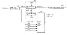
- FIG. 1is a block diagram of a conventional image sensor capable of storing addresses of defective pixels by using the fuse blowing technique.
- the image sensorincludes a pixel array 100 , a line buffer 200 , an image signal processing unit 300 , a defective pixel address storing unit 500 , a control and interface unit 400 and a defective pixel compensation unit 600 .
- the line buffer 200stores data transmitted from the pixel array 100 and the image signal processing unit 300 performs a signal processing to improve the performance of the image sensor in response to outputs of the line buffer 200 .
- the defective pixel address storing unit 500stores addresses of defective pixels, which are detected from a wafer level test, by using the fuse blowing technology.
- the control and interface unit 400receives the address information of the defective pixels from the defective pixel address storing unit 500 and controls the whole operation of the image sensor. Also, the control and interface unit 400 manages an interface with an external system.
- the defective pixel compensation unit 600receives the address information of the defective pixels from the defective pixel address storing unit 500 , control signals from the control and interface unit 400 and pixel data from the line buffer 200 . Therefore, the defective pixel compensation unit 600 compensates the data of the defective pixels by replacing the defective pixel data with normal pixel data around the defective pixels and outputs the replaced pixel data to the image signal processing unit 300 .
- the defective pixel address storing unit 500includes a row address selection block 510 , a column address storage block 520 and a selection bit block 530 .
- the row address selection block 510stores information for whether or not defect pixels exist for each row of the pixel array 100 by on/off of fuse therein and outputs a row address selection signal RASS to the control and interface unit 400 .
- the column address storage block 520stores information for column addresses of the defective pixels and outputs a column address signal CAS to the defective pixel compensation unit 600 .
- the selection bit block 530stores information for correctly matching information stored in the row address selection block 510 and the column address storage block 520 and outputs a matching signal to the control and interface unit 400 .
- an image sensorincluding a storage block for storing a plurality of pixel data which is transmitted from a pixel array block; a switching block for delivering a first pixel data from the storage block in response to a first control signal PASS; a defect pixel repairing block which is controlled by the first, a second, a third, a forth and a fifth control signals PASS, DPCA, MS, ISCA and Line End in order to receive surrounding pixel data having the first pixel data from the storage block and the first pixel data from the switching block and output a revised pixel data by using the first pixel data or the surrounding pixel data; and a image signal handling block for receiving the first pixel data outputted from the switching block or the revised pixel data outputted from the defect pixel repairing block and operating an image process in order to improvement of the image sensor.
- FIG. 1is a block diagram describing a conventional image sensor
- FIG. 2is a block diagram describing a defect pixel compensation block and its surrounding blocks included in the image sensor shown in FIG. 1;
- FIG. 3is a block diagram showing the defect pixel compensation block in detail
- FIG. 4is an example describing surrounding pixel data having the pixel data
- FIG. 5is a circuit diagram showing a revised pixel selecting unit 650 ;
- FIG. 6is a circuit diagram showing a DPCA controlling unit 630 ;
- FIGS. 7A and 7Bare tables depicting a DPCA updating signal changed in response to a current matching signal MS 1 and a next matching signal MS 2 which are inputted to the DPCA controlling unit 630 ;
- FIGS. 8 and 9are timing diagrams showing operation of the image sensor having a defect pixel.
- FIG. 2is a block diagram describing a defect pixel revision unit included in the image sensor shown in FIG. 1.
- the defect pixel revision unitincludes a switching block 700 and a defect pixel compensation block 600 . More particularly, there is described a control signal flow around the defect pixel compensation block 600 .
- the defect pixel compensation block 600is for repairing and compensating the pixel data of the defect pixels by using an address of the defect pixel which is stored in a defect pixel address storage block 500 by fuse blowing technology.
- an image sensor in accordance with the present inventionfurther includes the switching block 700 .
- the switching block 700is controlled by a defect pixel column address selecting signal RASS, i.e., the RASS is generated from the column address selecting block 510 included in the defect pixel address storage block 500 and inputted through the control and interface block 400 , for transmitting a pixel data PIXEL(i,j) outputted from the pixel line memory block 200 in response to an current address.
- RASSdefect pixel column address selecting signal
- the image sensor in accordance with the present inventionfurther includes a defect pixel compensation block 600 for receiving surrounding pixel data PIXEL[I,J] having the pixel data PIXEL(i,j) from the pixel line memory block 200 and the pixel data PIXEL(i,j) from the switching block 700 and outputting a revised pixel data PIXEL*(i,j) by using the pixel data PIXEL(i,j) or the surrounding pixel data PIXEL[I,J].
- a defect pixel compensation block 600for receiving surrounding pixel data PIXEL[I,J] having the pixel data PIXEL(i,j) from the pixel line memory block 200 and the pixel data PIXEL(i,j) from the switching block 700 and outputting a revised pixel data PIXEL*(i,j) by using the pixel data PIXEL(i,j) or the surrounding pixel data PIXEL[I,J].
- the image sensor in accordance with the present inventionhas several control signals, i.e., RASS, DPCA, MS, ISCA and LINE-END.
- a defect pixel column address DPCAis outputted from a column address storage block 520 .
- An image sensor column address ISCAis a column address signal which is serially supplied in a chip.
- a matching signal MSis generated by a selecting bit block 530 and inputted through the control and interface block 400 .
- a last column signal LINE-ENDis usually in logical ‘0’ but, only at the last column in each row, in logical ‘1’.
- the image sensor in accordance with the present inventionfurther includes the image signal handling block 300 for receiving the pixel data PIXEL(i,j) outputted from the switching block 700 or one of the pixel data PIXEL(i,j) and the revised pixel data PIXEL*(i,j) outputted from the defect pixel compensation block 600 and operating an image process in order to improvement of the image sensor.
- the switching block 700includes a first switching unit SW 1 controlled by the defect pixel column address selecting signal RASS and the inverse defect pixel column address selecting signal /RASS in order to transmit the pixel data PIXEL(i,j) to the image signal handling block 300 and a second switching unit SW 2 controlled by the defect pixel column address selecting signal RASS and the inverse defect pixel column address selecting signal /RASS in order to transmit the pixel data PIXEL(i,j) to the defect pixel compensation block 600 .
- the first and second switching blocks SW 1 and SW 2respectively have a transmission gate which is composed of a pair of NMOS transistor and PMOS transistor.
- the first switching unit SW 1is off and the second switching unit SW 2 is on.
- the revised pixel data PIXEL*(i,j) outputted from the defect pixel compensation block 600is inputted to the image signal handling block 300 .
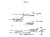
- FIG. 3is a block diagram showing the defect pixel compensation block 600 in detail.
- the defect pixel compensation block 600 of the image sensor in accordance with the present inventionincludes a DPCA temporary storage unit 610 for temporary storing the defect pixel column address DPCA, a column address detecting unit 620 for comparing the defect pixel column address DPCA outputted from the DPCA temporary storage unit with the image sensor column address ISCA and generating a DPCA detecting signal showing whether or not the defect pixel column address DPCA is equal to the image sensor column address ISCA, a DPCA controlling unit 630 for outputting an next defect pixel column address DPCA to the DPCA temporary storage unit 610 in response to the DPCA detecting signal, the matching signal MS and the last column signal LINE-END, a defect pixel changing unit 640 for receiving the surrounding pixel data PIXEL[I,J] and generating the revised pixel data PIXEL*(i,j), a revised pixel selecting unit 650 for selectively outputting the revised pixel data PIXEL*(i,j) or the
- defect pixel compensation block 600is depicted in detail.
- the column address detecting unit 620compares the image sensor column address ISCA which is serially outputted from the control and interface block 400 with the defect pixel column address DPCA which is already stored in the DPCA temporary storage unit 610 . If the ISCA is same to the DPCA, the DPCA detecting signal is in logical ‘1’. Otherwise, the DPCA detecting signal is in logical ‘0’.
- the revised pixel selecting unit 650In case when the DPCA detecting signal is in logical ‘0’, there is not any defect pixel at that row. So, the revised pixel selecting unit 650 outputs the pixel data PIXEL(i,j) outputted from the pixel line memory block 200 . However, if the DPCA detecting signal is in logical ‘1’, there is defect pixel at that row. Thus, the revised pixel selecting unit 650 outputs the revised pixel data PIXEL*(i,j) outputted from the defect pixel changing unit 640 .
- FIG. 4describes the surrounding pixel data PIXEL[I,J] having the pixel data PIXEL(i,j).
- the surrounding pixel data PIXEL[I,J]includes eight pixel data PIXEL(i ⁇ 1,j ⁇ 1) to PIXEL(i+1,j+1) except the pixel data PIXEL(i,j).
- oneis a way using average of the eight pixel data PIXEL(i ⁇ 1,j ⁇ 1) to PIXEL(i+1,j+1), and another is to substitute the pixel data PIXEL(i,j) with one of the eight pixel data PIXEL(i ⁇ 1,j ⁇ 1) to PIXEL(i+1,j+1).
- Structure of the defect pixel changing unit 640can be changed in response to how to generate the revised pixel data PIXEL*(i,j).
- FIG. 5is a circuit diagram showing the revised pixel selecting unit 650 .
- the revised pixel selecting unit 650includes two transmission gates controlled by both the DPCA detecting signal and the inverse DPCA detecting signal for selectively delivering either the pixel data PIXEL(i,j) or the revised pixel data PIXEL*(i,j).
- FIG. 6is a circuit diagram showing the DPCA controlling unit 630 .
- the DPCA controlling unit 630includes a first D flip-flop 631 for receiving the matching signal MS and outputting a current matching signal MS 1 , a second D flip-flop 632 for receiving the current matching signal MS 1 and outputting a next matching signal MS 2 , a first AND gate 633 for receiving the current matching signal MS 1 and the next matching signal MS 2 , an OR gate 634 for receiving the current matching signal MS 1 and an output of the first AND gate, a second AND gate 635 for receiving the DPCA detecting signal and an output of the OR gate, and a XOR gate 636 for receiving the last column signal LINE-END and an output of the second AND gate 635 and outputting an DPCA control signal for updating the defect pixel column address DPCA.
- the DPCA controlling unit 630includes the first and second D flip-flops 631 and 632 for storing the current value and next value of the matching signal MS 1 and MS 2 . There is a reason that condition of updating the defect pixel column address DPCA stored in the DPCA temporary storage unit 610 is changed in response to the current value and next value of the matching signal MS 1 and MS 2 .
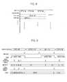
- FIGS. 7A and 7Bare tables depicting the DPCA control signal changed in response to the current matching signal MS 1 and the next matching signal MS 2 which are inputted to the DPCA controlling unit 630 .
- FIG. 7Ashows the DPCA control signal if the last column signal LINE-END is in logical ‘0’.
- the DPCA detecting signalis in logical ‘0’
- the DPCA control signal outputted from the DPCA controlling unit 630is hold. Namely, in case when, in the column address detecting unit 620 , the DPCA is not equal to the ISCA, the DPCA control signal is in logical ‘0’ and, unrelated to matching signals MS 1 and MS 2 , the defect pixel column address DPCA of the DPCA temporary storage unit 610 is not changed.
- the DPCA control signalis in logical ‘1’ if the matching signals (MS 1 , MS 2 ) are (1,0) or (1,1).
- the defect pixel column address DPCA of the DPCA temporary storage unit 610is changed.
- the defect pixel column address DPCA of the DPCA temporary storage unit 610is not changed if the matching signals (MS 1 , MS 2 ) are (0,0) or (0,1).
- the matching signals(MS 1 , MS 2 ) are (0,0) or (0,1), it means that there is just one defect pixel at a row or the last pixel at the row is a defect pixel.
- the defect pixel column address DPCA of the DPCA temporary storage unit 610is changed by making the DPCA control signal is in logical ‘1’, it can be occurred that normal pixel is repaired and compensated. So, for preventing mal-operation that normal pixel is repaired and compensated, the DPCA control signal keeps in logical ‘0’.
- FIG. 7Bshows the DPCA updating signal if the last column signal LINE-END is in logical ‘1’.
- the DPCA control signalis in logical ‘1’ if U node shown in FIG. 6 is in logical ‘1’. So, the defect pixel column address DPCA of the DPCA temporary storage unit 610 is changed. Otherwise, if U node shown in FIG. 6 is in logical ‘1’ and the prior last column signal LINE-END is in logical ‘0’, the DPCA control signal keeps in logical ‘0’ because the defect pixel column address DPCA is updated without any delay.
- FIGS. 8 and 9are timing diagrams showing operation of the image sensor having a defect pixel.
- the defect pixel column address selecting signal RASSis in logical high and the prior last column signal LINE-END is in logical high at the last column in each line.
- the DPCA 1 , DPCA 2 and DPCA 3 existed in the first lineis compensated to make the DPCA detecting signal outputted from the column address detecting unit 620 in logical high.
- the DPCA detecting signal and the DPCA control signalare in logical high.
- the DPCA detecting signalis in logical high but the DPCA control signal keeps in logical low until the last column signal LINE-END is in logical high at the last column in the first line. Then, if the last column signal LINE-END is in logical high, the DPCA control signal in response to the DPCA 3 is changed in logical high.
- the DPCA control signals in response to the DPCA 4 in the third line and the DPCA 5 in the forth lineare in logical high if the last column signal LINE-END is in logical high.
- the image sensor in accordance with the present inventiondoes not need an additional EEPROM for storing addresses of defect pixels because the addresses of defect pixels are stored by the fuse blowing technology and the stored addresses are used for compensating pixel data of the defect pixels.
- the present inventioncan reduce purchasing cost of the image sensor because of increasing a factional yield of fabricating the image sensor.
Landscapes
- Engineering & Computer Science (AREA)
- Multimedia (AREA)
- Signal Processing (AREA)
- Transforming Light Signals Into Electric Signals (AREA)
- Image Input (AREA)
- Facsimile Heads (AREA)
- Facsimile Scanning Arrangements (AREA)
Abstract
Description
- The present invention relates to an image sensor; and, more particularly, to a repair technique for revising a defect pixel of the image sensor detected by a test.[0001]
- An image sensor is a device for picking up light images by using a semiconductor property to react to the light. Namely, the image sensor is a device whose pixels detect different brightness and wavelengths of the light which is reflected from each object and which converts those detected values into corresponding electrical values. The image sensor changes the electric values into voltage levels to which signal processing can be performed. Recently, VGA (640×480 pixels) and SVGA (800×600 pixels) have been mainly used in image sensors. As digital still cameras come into universal use, an image sensor of a mega-pixel level (having more than one million pixels) will be commonly used. Therefore, in the future, the image sensor having at least one million pixels may be usually used because a digital still camera becomes an ordinary device. Thus, a technology for the image sensor having over mega-pixel is necessary to secure a market of a next generation image sensor.[0002]
- Meanwhile, as the number of pixels in the image sensor increases, the number of defective pixels, which are generated by the difficulty in a fabricating process, also increases. The defective pixels should be repaired to reduce the fabricating cost and to increase the yield.[0003]
- A grade of the image sensor and a price thereof are determined according to the number of the defective pixels and, if image sensors include the defective pixels without being repaired, the fabricating cost of the image sensor is increased because the yield is decreased.[0004]
- In order to solve the above problem, a product employing the image sensor chip having one or more defective pixels, such as the digital still camera or the like, is provided with a post test method. The post test method includes the step of testing each pixel; recording addresses of the defective pixels in an EEPROM; and then compensating data corresponding to the defective pixels, so that the image sensor having the defective pixels can be used in the product as a normal image sensor.[0005]
- However, since this test is carried out separately from a test in a wafer-level test, a period of developing a product employing the image sensor is increased. Also, since the EEPROM has to be additionally embedded in the product, a size of the product becomes bigger and its manufacturing cost will be increased.[0006]
- On the other hand, in case a manufacturer of the image sensor chip directly detects defective pixels through the wafer-level test and records the addresses of the defective pixels and then packages the EEPROM with the image sensor, the product developing can be shortened because a company can use the image sensor chip without an additional post pixel test. However, since it is required to perform an extra process for fabricating the EEPROM in addition to the image sensor fabricating process, the fabricating process of the image sensor becomes complicated and its fabrication cost is increased.[0007]
- For resolving this problem, an image sensor employing a fuse blowing technique is disclosed in a commonly owned copending application, U.S. Ser. No. 10/189,942, filed on Jul. 3, 2002, entitled “IMAGE SENSOR WITH DEFECT PIXEL ADDRESS STORAGE”.[0008]
- FIG. 1 is a block diagram of a conventional image sensor capable of storing addresses of defective pixels by using the fuse blowing technique.[0009]
- As shown, the image sensor includes a[0010]
pixel array 100, aline buffer 200, an imagesignal processing unit 300, a defective pixeladdress storing unit 500, a control andinterface unit 400 and a defectivepixel compensation unit 600. - The[0011]
line buffer 200 stores data transmitted from thepixel array 100 and the imagesignal processing unit 300 performs a signal processing to improve the performance of the image sensor in response to outputs of theline buffer 200. The defective pixeladdress storing unit 500 stores addresses of defective pixels, which are detected from a wafer level test, by using the fuse blowing technology. The control andinterface unit 400 receives the address information of the defective pixels from the defective pixeladdress storing unit 500 and controls the whole operation of the image sensor. Also, the control andinterface unit 400 manages an interface with an external system. The defectivepixel compensation unit 600 receives the address information of the defective pixels from the defective pixeladdress storing unit 500, control signals from the control andinterface unit 400 and pixel data from theline buffer 200. Therefore, the defectivepixel compensation unit 600 compensates the data of the defective pixels by replacing the defective pixel data with normal pixel data around the defective pixels and outputs the replaced pixel data to the imagesignal processing unit 300. - In FIG. 1, the defective pixel[0012]
address storing unit 500 includes a rowaddress selection block 510, a columnaddress storage block 520 and aselection bit block 530. The rowaddress selection block 510 stores information for whether or not defect pixels exist for each row of thepixel array 100 by on/off of fuse therein and outputs a row address selection signal RASS to the control andinterface unit 400. The columnaddress storage block 520 stores information for column addresses of the defective pixels and outputs a column address signal CAS to the defectivepixel compensation unit 600. Theselection bit block 530 stores information for correctly matching information stored in the rowaddress selection block 510 and the columnaddress storage block 520 and outputs a matching signal to the control andinterface unit 400. - However, there is needed a more efficient circuit for implementing the detective[0013]
pixel compensation unit 600. - It is, therefore, an object of the present invention to provide a circuit and method capable of implementing the detective pixel compensation unit.[0014]
- In accordance with an aspect of the present invention, there is provided an image sensor including a storage block for storing a plurality of pixel data which is transmitted from a pixel array block; a switching block for delivering a first pixel data from the storage block in response to a first control signal PASS; a defect pixel repairing block which is controlled by the first, a second, a third, a forth and a fifth control signals PASS, DPCA, MS, ISCA and Line End in order to receive surrounding pixel data having the first pixel data from the storage block and the first pixel data from the switching block and output a revised pixel data by using the first pixel data or the surrounding pixel data; and a image signal handling block for receiving the first pixel data outputted from the switching block or the revised pixel data outputted from the defect pixel repairing block and operating an image process in order to improvement of the image sensor.[0015]
- The above and other objects and features of the instant invention will become apparent from the following description of preferred embodiments taken in conjunction with the accompanying drawings, in which:[0016]
- FIG. 1 is a block diagram describing a conventional image sensor;[0017]
- FIG. 2 is a block diagram describing a defect pixel compensation block and its surrounding blocks included in the image sensor shown in FIG. 1;[0018]
- FIG. 3 is a block diagram showing the defect pixel compensation block in detail;[0019]
- FIG. 4 is an example describing surrounding pixel data having the pixel data;[0020]
- FIG. 5 is a circuit diagram showing a revised[0021]
pixel selecting unit 650; - FIG. 6 is a circuit diagram showing a DPCA controlling[0022]
unit 630; - FIGS. 7A and 7B are tables depicting a DPCA updating signal changed in response to a current matching signal MS[0023]1 and a next matching signal MS2 which are inputted to the DPCA controlling
unit 630; and - FIGS. 8 and 9 are timing diagrams showing operation of the image sensor having a defect pixel.[0024]
- Hereinafter, an inventive apparatus and method for repairing and compensating a pixel data of a defect pixel by repair operation using stored address of a defect pixel in an image sensor will be described in detail with reference to the accompanying drawings.[0025]
- FIG. 2 is a block diagram describing a defect pixel revision unit included in the image sensor shown in FIG. 1.[0026]
- As shown, the defect pixel revision unit includes a[0027]
switching block 700 and a defectpixel compensation block 600. More particularly, there is described a control signal flow around the defectpixel compensation block 600. The defectpixel compensation block 600 is for repairing and compensating the pixel data of the defect pixels by using an address of the defect pixel which is stored in a defect pixeladdress storage block 500 by fuse blowing technology. - In an image sensor disclosed in a commonly owned copending application, U.S. Ser. No. 10/189,942, filed on Jul. 3, 2002 and entitled “IMAGE SENSOR WITH DEFECT PIXEL ADDRESS STORAGE”, the control signals shown in FIGS. 1 and 2, i.e., RASS, DPCA, MS and the like are already described in detail. So, description about the control signals RASS, DPCA and MS is omitted and, herein, there is described how to repair and compensate pixel data of defect pixels.[0028]
- Referring to FIG. 2, an image sensor in accordance with the present invention further includes the[0029]
switching block 700. Theswitching block 700 is controlled by a defect pixel column address selecting signal RASS, i.e., the RASS is generated from the columnaddress selecting block 510 included in the defect pixeladdress storage block 500 and inputted through the control andinterface block 400, for transmitting a pixel data PIXEL(i,j) outputted from the pixelline memory block 200 in response to an current address. - In addition, the image sensor in accordance with the present invention further includes a defect[0030]
pixel compensation block 600 for receiving surrounding pixel data PIXEL[I,J] having the pixel data PIXEL(i,j) from the pixelline memory block 200 and the pixel data PIXEL(i,j) from theswitching block 700 and outputting a revised pixel data PIXEL*(i,j) by using the pixel data PIXEL(i,j) or the surrounding pixel data PIXEL[I,J]. - Herein, the image sensor in accordance with the present invention has several control signals, i.e., RASS, DPCA, MS, ISCA and LINE-END. A defect pixel column address DPCA is outputted from a column[0031]
address storage block 520. An image sensor column address ISCA is a column address signal which is serially supplied in a chip. A matching signal MS is generated by a selecting bit block530 and inputted through the control andinterface block 400. A last column signal LINE-END is usually in logical ‘0’ but, only at the last column in each row, in logical ‘1’. - In addition, the image sensor in accordance with the present invention further includes the image[0032]
signal handling block 300 for receiving the pixel data PIXEL(i,j) outputted from theswitching block 700 or one of the pixel data PIXEL(i,j) and the revised pixel data PIXEL*(i,j) outputted from the defectpixel compensation block 600 and operating an image process in order to improvement of the image sensor. - Hereinafter, the[0033]
switching block 700 is described in detail. Theswitching block 700 includes a first switching unit SW1 controlled by the defect pixel column address selecting signal RASS and the inverse defect pixel column address selecting signal /RASS in order to transmit the pixel data PIXEL(i,j) to the imagesignal handling block 300 and a second switching unit SW2 controlled by the defect pixel column address selecting signal RASS and the inverse defect pixel column address selecting signal /RASS in order to transmit the pixel data PIXEL(i,j) to the defectpixel compensation block 600. The first and second switching blocks SW1 and SW2 respectively have a transmission gate which is composed of a pair of NMOS transistor and PMOS transistor. - Thus, if there is the defect pixel at a line in the image sensor, i.e., the RASS is in logical ‘1’, the first switching unit SW[0034]1 is off and the second switching unit SW2 is on. As a result, the revised pixel data PIXEL*(i,j) outputted from the defect
pixel compensation block 600 is inputted to the imagesignal handling block 300. - FIG. 3 is a block diagram showing the defect[0035]
pixel compensation block 600 in detail. - As shown, the defect[0036]
pixel compensation block 600 of the image sensor in accordance with the present invention includes a DPCAtemporary storage unit 610 for temporary storing the defect pixel column address DPCA, a columnaddress detecting unit 620 for comparing the defect pixel column address DPCA outputted from the DPCA temporary storage unit with the image sensor column address ISCA and generating a DPCA detecting signal showing whether or not the defect pixel column address DPCA is equal to the image sensor column address ISCA, aDPCA controlling unit 630 for outputting an next defect pixel column address DPCA to the DPCAtemporary storage unit 610 in response to the DPCA detecting signal, the matching signal MS and the last column signal LINE-END, a defectpixel changing unit 640 for receiving the surrounding pixel data PIXEL[I,J] and generating the revised pixel data PIXEL*(i,j), a revisedpixel selecting unit 650 for selectively outputting the revised pixel data PIXEL*(i,j) or the pixel data PIXEL(i,j) in response to the DPCA detecting signal, and aswitch outputting unit 660 controlled by the defect pixel column address selecting signal RASS in order to selectively output an output of the revisedpixel selecting unit 650. - Hereinafter, the defect[0037]
pixel compensation block 600 is depicted in detail. - If the defect pixel column address selecting signal RASS is in logical ‘1’, i.e., there is a defect pixel at a row, the column[0038]
address detecting unit 620 compares the image sensor column address ISCA which is serially outputted from the control andinterface block 400 with the defect pixel column address DPCA which is already stored in the DPCAtemporary storage unit 610. If the ISCA is same to the DPCA, the DPCA detecting signal is in logical ‘1’. Otherwise, the DPCA detecting signal is in logical ‘0’. - In case when the DPCA detecting signal is in logical ‘0’, there is not any defect pixel at that row. So, the revised[0039]
pixel selecting unit 650 outputs the pixel data PIXEL(i,j) outputted from the pixelline memory block 200. However, if the DPCA detecting signal is in logical ‘1’, there is defect pixel at that row. Thus, the revisedpixel selecting unit 650 outputs the revised pixel data PIXEL*(i,j) outputted from the defectpixel changing unit 640. - FIG. 4 describes the surrounding pixel data PIXEL[I,J] having the pixel data PIXEL(i,j).[0040]
- Herein, referring to FIG. 4, operation of the defect[0041]
pixel changing unit 640 is described in detail. It is assumed that the surrounding pixel data PIXEL[I,J] includes eight pixel data PIXEL(i−1,j−1) to PIXEL(i+1,j+1) except the pixel data PIXEL(i,j). There are several methods of generating the revised pixel data PIXEL*(i,j). For instance, one is a way using average of the eight pixel data PIXEL(i−1,j−1) to PIXEL(i+1,j+1), and another is to substitute the pixel data PIXEL(i,j) with one of the eight pixel data PIXEL(i−1,j−1) to PIXEL(i+1,j+1). Structure of the defectpixel changing unit 640 can be changed in response to how to generate the revised pixel data PIXEL*(i,j). - FIG. 5 is a circuit diagram showing the revised[0042]
pixel selecting unit 650. The revisedpixel selecting unit 650 includes two transmission gates controlled by both the DPCA detecting signal and the inverse DPCA detecting signal for selectively delivering either the pixel data PIXEL(i,j) or the revised pixel data PIXEL*(i,j). - FIG. 6 is a circuit diagram showing the[0043]
DPCA controlling unit 630. TheDPCA controlling unit 630 includes a first D flip-flop 631 for receiving the matching signal MS and outputting a current matching signal MS1, a second D flip-flop 632 for receiving the current matching signal MS1 and outputting a next matching signal MS2, a first ANDgate 633 for receiving the current matching signal MS1 and the next matching signal MS2, an ORgate 634 for receiving the current matching signal MS1 and an output of the first AND gate, a second ANDgate 635 for receiving the DPCA detecting signal and an output of the OR gate, and aXOR gate 636 for receiving the last column signal LINE-END and an output of the second ANDgate 635 and outputting an DPCA control signal for updating the defect pixel column address DPCA. - As above statement, the[0044]
DPCA controlling unit 630 includes the first and second D flip-flops temporary storage unit 610 is changed in response to the current value and next value of the matching signal MS1 and MS2. - FIGS. 7A and 7B are tables depicting the DPCA control signal changed in response to the current matching signal MS[0045]1 and the next matching signal MS2 which are inputted to the
DPCA controlling unit 630. - FIG. 7A shows the DPCA control signal if the last column signal LINE-END is in logical ‘0’. In this case, if the DPCA detecting signal is in logical ‘0’, the DPCA control signal outputted from the[0046]
DPCA controlling unit 630 is hold. Namely, in case when, in the columnaddress detecting unit 620, the DPCA is not equal to the ISCA, the DPCA control signal is in logical ‘0’ and, unrelated to matching signals MS1 and MS2, the defect pixel column address DPCA of the DPCAtemporary storage unit 610 is not changed. Otherwise, in case when the DPCA detecting signal is in logical ‘1’, the DPCA control signal is in logical ‘1’ if the matching signals (MS1, MS2) are (1,0) or (1,1). As a result, the defect pixel column address DPCA of the DPCAtemporary storage unit 610 is changed. However, in this case, i.e., the DPCA detecting signal is in logical ‘1’, the defect pixel column address DPCA of the DPCAtemporary storage unit 610 is not changed if the matching signals (MS1, MS2) are (0,0) or (0,1). - If the matching signals (MS[0047]1, MS2) are (0,0) or (0,1), it means that there is just one defect pixel at a row or the last pixel at the row is a defect pixel. At this time, if the defect pixel column address DPCA of the DPCA
temporary storage unit 610 is changed by making the DPCA control signal is in logical ‘1’, it can be occurred that normal pixel is repaired and compensated. So, for preventing mal-operation that normal pixel is repaired and compensated, the DPCA control signal keeps in logical ‘0’. - FIG. 7B shows the DPCA updating signal if the last column signal LINE-END is in logical ‘1’. As shown, in case when the last column signal LINE-END is in logical ‘1’, the DPCA control signal is in logical ‘1’ if U node shown in FIG. 6 is in logical ‘1’. So, the defect pixel column address DPCA of the DPCA[0048]
temporary storage unit 610 is changed. Otherwise, if U node shown in FIG. 6 is in logical ‘1’ and the prior last column signal LINE-END is in logical ‘0’, the DPCA control signal keeps in logical ‘0’ because the defect pixel column address DPCA is updated without any delay. - FIGS. 8 and 9 are timing diagrams showing operation of the image sensor having a defect pixel.[0049]
- Referring to FIGS. 8 and 9, in a first, a third and a forth rows where the defect pixel exists, the defect pixel column address selecting signal RASS is in logical high and the prior last column signal LINE-END is in logical high at the last column in each line. The DPCA[0050]1, DPCA2 and DPCA3 existed in the first line is compensated to make the DPCA detecting signal outputted from the column
address detecting unit 620 in logical high. At this time, at the DPCA1 and DPCA2, the DPCA detecting signal and the DPCA control signal are in logical high. - However, at the DPCA[0051]3, i.e., the last defect pixel in the first row, the DPCA detecting signal is in logical high but the DPCA control signal keeps in logical low until the last column signal LINE-END is in logical high at the last column in the first line. Then, if the last column signal LINE-END is in logical high, the DPCA control signal in response to the DPCA3 is changed in logical high.
- As good as the DPCA[0052]3, the DPCA control signals in response to the DPCA4 in the third line and the DPCA5 in the forth line are in logical high if the last column signal LINE-END is in logical high.
- The image sensor in accordance with the present invention does not need an additional EEPROM for storing addresses of defect pixels because the addresses of defect pixels are stored by the fuse blowing technology and the stored addresses are used for compensating pixel data of the defect pixels. As a result, the present invention can reduce purchasing cost of the image sensor because of increasing a factional yield of fabricating the image sensor.[0053]
- While the present invention has been described with respect to the particular embodiments, it will be apparent to those skilled in the art that various changes and modifications may be made without departing from the spirit and scope of the invention as defined in the following claims.[0054]
Claims (7)
Applications Claiming Priority (2)
| Application Number | Priority Date | Filing Date | Title |
|---|---|---|---|
| KR2003-11468 | 2003-02-24 | ||
| KR10-2003-0011468AKR100535636B1 (en) | 2003-02-24 | 2003-02-24 | Defect pixel repairable image sensor |
Publications (2)
| Publication Number | Publication Date |
|---|---|
| US20040165089A1true US20040165089A1 (en) | 2004-08-26 |
| US7352395B2 US7352395B2 (en) | 2008-04-01 |
Family
ID=32866944
Family Applications (1)
| Application Number | Title | Priority Date | Filing Date |
|---|---|---|---|
| US10/748,643Active2026-01-20US7352395B2 (en) | 2003-02-24 | 2003-12-29 | Defect pixel repairable image sensor |
Country Status (3)
| Country | Link |
|---|---|
| US (1) | US7352395B2 (en) |
| JP (2) | JP2004260814A (en) |
| KR (1) | KR100535636B1 (en) |
Cited By (7)
| Publication number | Priority date | Publication date | Assignee | Title |
|---|---|---|---|---|
| US20070139740A1 (en)* | 2005-12-20 | 2007-06-21 | Fujitsu Limited | Image processing circuit and image processing method |
| US20070185676A1 (en)* | 2005-09-23 | 2007-08-09 | Delta Design, Inc. | Single camera three-point vision alignment system for a device handler |
| US20090289206A1 (en)* | 2008-05-23 | 2009-11-26 | Delta Design, Inc. | Camera based vision alignment with device group guiding for semiconductor device testing handlers |
| US20100017161A1 (en)* | 2008-07-16 | 2010-01-21 | Delta Design, Inc. | Vision alignment with multiple cameras and common coordinate at contactor for ic device testing handlers |
| US20110010122A1 (en)* | 2009-07-07 | 2011-01-13 | Delta Design, Inc. | Calibrating separately located cameras with a double sided visible calibration target for ic device testing handlers |
| US20110254982A1 (en)* | 2008-12-26 | 2011-10-20 | Phil Ki Seo | Method for detecting/correcting bad pixel in image sensor |
| US11122221B2 (en)* | 2016-02-26 | 2021-09-14 | Shenzhen Xpectvision Technology Co., Ltd. | Semiconductor image detector having redundant memory and/or memory bypass |
Families Citing this family (8)
| Publication number | Priority date | Publication date | Assignee | Title |
|---|---|---|---|---|
| US7796169B2 (en)* | 2004-04-20 | 2010-09-14 | Canon Kabushiki Kaisha | Image processing apparatus for correcting captured image |
| JP4440239B2 (en)* | 2006-08-18 | 2010-03-24 | 富士フイルム株式会社 | Distance image creation method, distance image sensor, and photographing apparatus |
| US20080100725A1 (en)* | 2006-10-27 | 2008-05-01 | Abadeer Wagdi W | Circuits for enhancing yield and performance of cmos imaging sensors |
| US20080215261A1 (en)* | 2006-10-27 | 2008-09-04 | International Business Machines Corporation | Design structure for enhancing yield and performance of cmos imaging sensors |
| US20090161470A1 (en)* | 2007-12-20 | 2009-06-25 | Micron Technology, Inc. | Circuit for dynamic readout of fused data in image sensors |
| JP5060535B2 (en)* | 2009-09-24 | 2012-10-31 | 株式会社東芝 | Image processing device |
| WO2015069566A1 (en)* | 2013-11-05 | 2015-05-14 | Arizona Board Of Regents For And On Behalf Of Arizona State University | Adaptive detection sensor array and method of providing and using the same |
| KR102737923B1 (en)* | 2020-02-26 | 2024-12-03 | 삼성전자주식회사 | Image sensing device and operating the same |
Citations (8)
| Publication number | Priority date | Publication date | Assignee | Title |
|---|---|---|---|---|
| US5392070A (en)* | 1991-11-26 | 1995-02-21 | Kabushiki Kaisha Toshiba | Apparatus for correcting faulty pixel signals by replacing the faulty pixel signals with normal pixel signals |
| US6002433A (en)* | 1995-08-29 | 1999-12-14 | Sanyo Electric Co., Ltd. | Defective pixel detecting circuit of a solid state image pick-up device capable of detecting defective pixels with low power consumption and high precision, and image pick-up device having such detecting circuit |
| US20030007081A1 (en)* | 2001-07-06 | 2003-01-09 | Oh-Bong Kwon | Image sensor with defective pixel address storage |
| US20030063202A1 (en)* | 2001-09-28 | 2003-04-03 | Matsushita Electric Industrial Co., Ltd. | Solid-state imaging apparatus |
| US6642960B1 (en)* | 1998-02-02 | 2003-11-04 | Olympus Optical Co., Ltd. | Image pickup apparatus |
| US6683643B1 (en)* | 1997-03-19 | 2004-01-27 | Konica Minolta Holdings, Inc. | Electronic camera capable of detecting defective pixel |
| US20040036783A1 (en)* | 2002-08-22 | 2004-02-26 | Barna Sandor L. | Asymmetric comparator for use in pixel oversaturation detection |
| US20040169746A1 (en)* | 1999-03-15 | 2004-09-02 | Chen Zhiliang Julian | Defective pixel filtering for digital imagers |
Family Cites Families (6)
| Publication number | Priority date | Publication date | Assignee | Title |
|---|---|---|---|---|
| JPS59122184A (en)* | 1982-12-28 | 1984-07-14 | Nec Corp | Solid-state image pickup device |
| JPH084326B2 (en)* | 1986-09-30 | 1996-01-17 | キヤノン株式会社 | Imaging device |
| JPH07336605A (en)* | 1994-06-13 | 1995-12-22 | Matsushita Electric Ind Co Ltd | Pixel defect correction device |
| JP3417792B2 (en)* | 1997-04-24 | 2003-06-16 | 東芝マイクロエレクトロニクス株式会社 | Analog signal selection circuit |
| JP4313860B2 (en)* | 1998-07-01 | 2009-08-12 | キヤノン株式会社 | Defective pixel correction apparatus and defective pixel correction method |
| JP4199874B2 (en)* | 1999-03-30 | 2008-12-24 | 富士フイルム株式会社 | Image processing apparatus and processing method |
- 2003
- 2003-02-24KRKR10-2003-0011468Apatent/KR100535636B1/ennot_activeExpired - Fee Related
- 2003-12-29USUS10/748,643patent/US7352395B2/enactiveActive
- 2004
- 2004-02-04JPJP2004028220Apatent/JP2004260814A/ennot_activeWithdrawn
- 2010
- 2010-06-21JPJP2010140818Apatent/JP5368382B2/ennot_activeExpired - Fee Related
Patent Citations (8)
| Publication number | Priority date | Publication date | Assignee | Title |
|---|---|---|---|---|
| US5392070A (en)* | 1991-11-26 | 1995-02-21 | Kabushiki Kaisha Toshiba | Apparatus for correcting faulty pixel signals by replacing the faulty pixel signals with normal pixel signals |
| US6002433A (en)* | 1995-08-29 | 1999-12-14 | Sanyo Electric Co., Ltd. | Defective pixel detecting circuit of a solid state image pick-up device capable of detecting defective pixels with low power consumption and high precision, and image pick-up device having such detecting circuit |
| US6683643B1 (en)* | 1997-03-19 | 2004-01-27 | Konica Minolta Holdings, Inc. | Electronic camera capable of detecting defective pixel |
| US6642960B1 (en)* | 1998-02-02 | 2003-11-04 | Olympus Optical Co., Ltd. | Image pickup apparatus |
| US20040169746A1 (en)* | 1999-03-15 | 2004-09-02 | Chen Zhiliang Julian | Defective pixel filtering for digital imagers |
| US20030007081A1 (en)* | 2001-07-06 | 2003-01-09 | Oh-Bong Kwon | Image sensor with defective pixel address storage |
| US20030063202A1 (en)* | 2001-09-28 | 2003-04-03 | Matsushita Electric Industrial Co., Ltd. | Solid-state imaging apparatus |
| US20040036783A1 (en)* | 2002-08-22 | 2004-02-26 | Barna Sandor L. | Asymmetric comparator for use in pixel oversaturation detection |
Cited By (11)
| Publication number | Priority date | Publication date | Assignee | Title |
|---|---|---|---|---|
| US20070185676A1 (en)* | 2005-09-23 | 2007-08-09 | Delta Design, Inc. | Single camera three-point vision alignment system for a device handler |
| US20070139740A1 (en)* | 2005-12-20 | 2007-06-21 | Fujitsu Limited | Image processing circuit and image processing method |
| US7978383B2 (en) | 2005-12-20 | 2011-07-12 | Fujitsu Semiconductor Limited | Image processing circuit and image processing method |
| US20090289206A1 (en)* | 2008-05-23 | 2009-11-26 | Delta Design, Inc. | Camera based vision alignment with device group guiding for semiconductor device testing handlers |
| US7842912B2 (en) | 2008-05-23 | 2010-11-30 | Delta Design, Inc. | Camera based vision alignment with device group guiding for semiconductor device testing handlers |
| US20100017161A1 (en)* | 2008-07-16 | 2010-01-21 | Delta Design, Inc. | Vision alignment with multiple cameras and common coordinate at contactor for ic device testing handlers |
| US8106349B2 (en)* | 2008-07-16 | 2012-01-31 | Delta Design, Inc. | Vision alignment with multiple cameras and common coordinate at contactor for IC device testing handlers |
| US20110254982A1 (en)* | 2008-12-26 | 2011-10-20 | Phil Ki Seo | Method for detecting/correcting bad pixel in image sensor |
| US8913163B2 (en)* | 2008-12-26 | 2014-12-16 | Lg Innotek Co., Ltd. | Method for detecting/correcting bad pixel in image sensor |
| US20110010122A1 (en)* | 2009-07-07 | 2011-01-13 | Delta Design, Inc. | Calibrating separately located cameras with a double sided visible calibration target for ic device testing handlers |
| US11122221B2 (en)* | 2016-02-26 | 2021-09-14 | Shenzhen Xpectvision Technology Co., Ltd. | Semiconductor image detector having redundant memory and/or memory bypass |
Also Published As
| Publication number | Publication date |
|---|---|
| KR20040076124A (en) | 2004-08-31 |
| JP2010220254A (en) | 2010-09-30 |
| US7352395B2 (en) | 2008-04-01 |
| JP5368382B2 (en) | 2013-12-18 |
| KR100535636B1 (en) | 2005-12-08 |
| JP2004260814A (en) | 2004-09-16 |
Similar Documents
| Publication | Publication Date | Title |
|---|---|---|
| US7027089B2 (en) | Image sensor with defective pixel address storage | |
| JP5368382B2 (en) | Image sensor with defective pixel compensation function | |
| US6518945B1 (en) | Replacing defective circuit elements by column and row shifting in a flat-panel display | |
| CA1160342A (en) | Redundancy scheme for a dynamic ram | |
| US7358966B2 (en) | Selective update of micro-electromechanical device | |
| US6940765B2 (en) | Repair apparatus and method for semiconductor memory device to be selectively programmed for wafer-level test or post package test | |
| US5448578A (en) | Electrically erasable and programmable read only memory with an error check and correction circuit | |
| US4812680A (en) | High voltage detecting circuit | |
| EP1364360A2 (en) | Self diagnostic and repair in matrix display panel | |
| US6202180B1 (en) | Semiconductor memory capable of relieving a defective memory cell by exchanging addresses | |
| US6026036A (en) | Synchronous semiconductor memory device having set up time of external address signal reduced | |
| US20080251887A1 (en) | Serial system for blowing antifuses | |
| JPH11353892A (en) | Redundant de-enabling circuit of semiconductor memory device | |
| JPH0683716A (en) | Electrically rewritable non-volatile memory | |
| US20060227617A1 (en) | Semiconductor device and semiconductor integrated circuit | |
| US20080100725A1 (en) | Circuits for enhancing yield and performance of cmos imaging sensors | |
| EP0514164B1 (en) | Efficiency improved DRAM row redundancy circuit | |
| KR102845460B1 (en) | A display device including a cell matrix | |
| US8370708B2 (en) | Data error measuring circuit for semiconductor memory apparatus | |
| KR100460768B1 (en) | Image Sensor with defect pixel address storage block | |
| KR960002011B1 (en) | Redundancy circuit for semiconductor memory device | |
| KR20020068768A (en) | Semiconductor device having built-in self repair circuit for embedded memory | |
| KR100521030B1 (en) | Apparatus for concealment of defective pixel in image sensor | |
| KR100664860B1 (en) | Image sensor for defective pixel compensation | |
| US12283329B2 (en) | Electronic fuse circuit and method for electronic fuse circuit |
Legal Events
| Date | Code | Title | Description |
|---|---|---|---|
| AS | Assignment | Owner name:HYNIX SEMICONDUCTOR INC., KOREA, REPUBLIC OF Free format text:ASSIGNMENT OF ASSIGNORS INTEREST;ASSIGNOR:AN, HYUN-JOO;REEL/FRAME:015679/0015 Effective date:20031222 | |
| AS | Assignment | Owner name:MAGNACHIP SEMICONDUCTOR, LTD., KOREA, REPUBLIC OF Free format text:ASSIGNMENT OF ASSIGNORS INTEREST;ASSIGNOR:HYNIX SEMICONDUCTOR, INC.;REEL/FRAME:016216/0649 Effective date:20041004 | |
| FEPP | Fee payment procedure | Free format text:PAYOR NUMBER ASSIGNED (ORIGINAL EVENT CODE: ASPN); ENTITY STATUS OF PATENT OWNER: LARGE ENTITY | |
| STCF | Information on status: patent grant | Free format text:PATENTED CASE | |
| AS | Assignment | Owner name:U.S. BANK NATIONAL ASSOCIATION, AS COLLATERAL TRUS Free format text:AFTER-ACQUIRED INTELLECTUAL PROPERTY KUN-PLEDGE AGREEMENT;ASSIGNOR:MAGNACHIP SEMICONDUCTOR, LTD.;REEL/FRAME:022277/0133 Effective date:20090217 | |
| AS | Assignment | Owner name:CROSSTEK CAPITAL, LLC, DELAWARE Free format text:ASSIGNMENT OF ASSIGNORS INTEREST;ASSIGNOR:MAGNACHIP SEMICONDUCTOR, LTD.;REEL/FRAME:022764/0270 Effective date:20090514 Owner name:CROSSTEK CAPITAL, LLC,DELAWARE Free format text:ASSIGNMENT OF ASSIGNORS INTEREST;ASSIGNOR:MAGNACHIP SEMICONDUCTOR, LTD.;REEL/FRAME:022764/0270 Effective date:20090514 | |
| AS | Assignment | Owner name:MAGNACHIP SEMICONDUCTOR, LTD., KOREA, REPUBLIC OF Free format text:PARTIAL RELEASE OF SECURITY INTEREST;ASSIGNOR:U.S. BANK NATIONAL ASSOCIATION, AS COLLATERAL TRUSTEE;REEL/FRAME:023075/0054 Effective date:20090527 Owner name:MAGNACHIP SEMICONDUCTOR, LTD.,KOREA, REPUBLIC OF Free format text:PARTIAL RELEASE OF SECURITY INTEREST;ASSIGNOR:U.S. BANK NATIONAL ASSOCIATION, AS COLLATERAL TRUSTEE;REEL/FRAME:023075/0054 Effective date:20090527 | |
| FEPP | Fee payment procedure | Free format text:PAYOR NUMBER ASSIGNED (ORIGINAL EVENT CODE: ASPN); ENTITY STATUS OF PATENT OWNER: LARGE ENTITY Free format text:PAYER NUMBER DE-ASSIGNED (ORIGINAL EVENT CODE: RMPN); ENTITY STATUS OF PATENT OWNER: LARGE ENTITY | |
| AS | Assignment | Owner name:INTELLECTUAL VENTURES II LLC, DELAWARE Free format text:MERGER;ASSIGNOR:CROSSTEK CAPITAL, LLC;REEL/FRAME:026637/0632 Effective date:20110718 | |
| FPAY | Fee payment | Year of fee payment:4 | |
| FPAY | Fee payment | Year of fee payment:8 | |
| MAFP | Maintenance fee payment | Free format text:PAYMENT OF MAINTENANCE FEE, 12TH YEAR, LARGE ENTITY (ORIGINAL EVENT CODE: M1553); ENTITY STATUS OF PATENT OWNER: LARGE ENTITY Year of fee payment:12 |