US20040163590A1 - In-situ health check of liquid injection vaporizer - Google Patents
In-situ health check of liquid injection vaporizerDownload PDFInfo
- Publication number
- US20040163590A1 US20040163590A1US10/374,571US37457103AUS2004163590A1US 20040163590 A1US20040163590 A1US 20040163590A1US 37457103 AUS37457103 AUS 37457103AUS 2004163590 A1US2004163590 A1US 2004163590A1
- Authority
- US
- United States
- Prior art keywords
- injection valve
- carrier gas
- pressure
- liquid precursor
- fluid communication
- Prior art date
- Legal status (The legal status is an assumption and is not a legal conclusion. Google has not performed a legal analysis and makes no representation as to the accuracy of the status listed.)
- Abandoned
Links
- 238000002347injectionMethods0.000titleclaimsabstractdescription117
- 239000007924injectionSubstances0.000titleclaimsabstractdescription117
- 239000007788liquidSubstances0.000titleclaimsdescription72
- 238000011065in-situ storageMethods0.000titledescription3
- 239000006200vaporizerSubstances0.000title1
- 239000012705liquid precursorSubstances0.000claimsabstractdescription62
- 238000011144upstream manufacturingMethods0.000claimsabstractdescription22
- 239000004065semiconductorSubstances0.000claimsabstractdescription15
- 239000007789gasSubstances0.000claimsdescription157
- 238000000034methodMethods0.000claimsdescription123
- 239000012159carrier gasSubstances0.000claimsdescription105
- 238000012545processingMethods0.000claimsdescription97
- 238000004891communicationMethods0.000claimsdescription54
- 239000012530fluidSubstances0.000claimsdescription39
- 238000005229chemical vapour depositionMethods0.000claimsdescription34
- 230000008016vaporizationEffects0.000claimsdescription33
- 239000000758substrateSubstances0.000claimsdescription23
- 239000000203mixtureSubstances0.000claimsdescription16
- 239000000463materialSubstances0.000claimsdescription8
- 235000012431wafersNutrition0.000abstractdescription25
- 238000012544monitoring processMethods0.000abstractdescription15
- 238000001514detection methodMethods0.000abstractdescription7
- 238000004519manufacturing processMethods0.000abstractdescription6
- 238000012937correctionMethods0.000abstractdescription2
- 230000008569processEffects0.000description105
- 238000009834vaporizationMethods0.000description23
- BOTDANWDWHJENH-UHFFFAOYSA-NTetraethyl orthosilicateChemical compoundCCO[Si](OCC)(OCC)OCCBOTDANWDWHJENH-UHFFFAOYSA-N0.000description14
- SWQJXJOGLNCZEY-UHFFFAOYSA-Nhelium atomChemical compound[He]SWQJXJOGLNCZEY-UHFFFAOYSA-N0.000description14
- 238000002156mixingMethods0.000description13
- 239000001307heliumSubstances0.000description12
- 229910052734heliumInorganic materials0.000description12
- 230000001276controlling effectEffects0.000description9
- 238000004140cleaningMethods0.000description8
- 238000010586diagramMethods0.000description8
- 238000000151depositionMethods0.000description7
- 238000009826distributionMethods0.000description7
- 238000010438heat treatmentMethods0.000description7
- 238000004590computer programMethods0.000description6
- 230000008021depositionEffects0.000description6
- 230000007246mechanismEffects0.000description6
- VYPSYNLAJGMNEJ-UHFFFAOYSA-NSilicium dioxideChemical compoundO=[Si]=OVYPSYNLAJGMNEJ-UHFFFAOYSA-N0.000description4
- 230000008901benefitEffects0.000description4
- ILAHWRKJUDSMFH-UHFFFAOYSA-Nboron tribromideChemical compoundBrB(Br)BrILAHWRKJUDSMFH-UHFFFAOYSA-N0.000description4
- 239000000919ceramicSubstances0.000description4
- 238000006243chemical reactionMethods0.000description4
- 238000012423maintenanceMethods0.000description4
- XHXFXVLFKHQFAL-UHFFFAOYSA-Nphosphoryl trichlorideChemical compoundClP(Cl)(Cl)=OXHXFXVLFKHQFAL-UHFFFAOYSA-N0.000description4
- 239000002243precursorSubstances0.000description4
- 238000005086pumpingMethods0.000description4
- IJGRMHOSHXDMSA-UHFFFAOYSA-NAtomic nitrogenChemical compoundN#NIJGRMHOSHXDMSA-UHFFFAOYSA-N0.000description3
- 238000005247getteringMethods0.000description3
- 238000010926purgeMethods0.000description3
- XKRFYHLGVUSROY-UHFFFAOYSA-NArgonChemical compound[Ar]XKRFYHLGVUSROY-UHFFFAOYSA-N0.000description2
- PXHVJJICTQNCMI-UHFFFAOYSA-NNickelChemical compound[Ni]PXHVJJICTQNCMI-UHFFFAOYSA-N0.000description2
- PNEYBMLMFCGWSK-UHFFFAOYSA-Naluminium oxideInorganic materials[O-2].[O-2].[O-2].[Al+3].[Al+3]PNEYBMLMFCGWSK-UHFFFAOYSA-N0.000description2
- 238000005530etchingMethods0.000description2
- 230000006870functionEffects0.000description2
- 239000011261inert gasSubstances0.000description2
- VYIRVGYSUZPNLF-UHFFFAOYSA-Nn-(tert-butylamino)silyl-2-methylpropan-2-amineChemical compoundCC(C)(C)N[SiH2]NC(C)(C)CVYIRVGYSUZPNLF-UHFFFAOYSA-N0.000description2
- 239000011148porous materialSubstances0.000description2
- 235000012239silicon dioxideNutrition0.000description2
- 239000000377silicon dioxideSubstances0.000description2
- 239000011343solid materialSubstances0.000description2
- CZDYPVPMEAXLPK-UHFFFAOYSA-NtetramethylsilaneChemical compoundC[Si](C)(C)CCZDYPVPMEAXLPK-UHFFFAOYSA-N0.000description2
- XJDNKRIXUMDJCW-UHFFFAOYSA-Jtitanium tetrachlorideChemical compoundCl[Ti](Cl)(Cl)ClXJDNKRIXUMDJCW-UHFFFAOYSA-J0.000description2
- 238000012546transferMethods0.000description2
- WRECIMRULFAWHA-UHFFFAOYSA-Ntrimethyl borateChemical compoundCOB(OC)OCWRECIMRULFAWHA-UHFFFAOYSA-N0.000description2
- WVLBCYQITXONBZ-UHFFFAOYSA-Ntrimethyl phosphateChemical compoundCOP(=O)(OC)OCWVLBCYQITXONBZ-UHFFFAOYSA-N0.000description2
- CYTQBVOFDCPGCX-UHFFFAOYSA-Ntrimethyl phosphiteChemical compoundCOP(OC)OCCYTQBVOFDCPGCX-UHFFFAOYSA-N0.000description2
- WZJUBBHODHNQPW-UHFFFAOYSA-N2,4,6,8-tetramethyl-1,3,5,7,2$l^{3},4$l^{3},6$l^{3},8$l^{3}-tetraoxatetrasilocaneChemical compoundC[Si]1O[Si](C)O[Si](C)O[Si](C)O1WZJUBBHODHNQPW-UHFFFAOYSA-N0.000description1
- PIGFYZPCRLYGLF-UHFFFAOYSA-NAluminum nitrideChemical compound[Al]#NPIGFYZPCRLYGLF-UHFFFAOYSA-N0.000description1
- BTBUEUYNUDRHOZ-UHFFFAOYSA-NBorateChemical compound[O-]B([O-])[O-]BTBUEUYNUDRHOZ-UHFFFAOYSA-N0.000description1
- YYKBKTFUORICGA-UHFFFAOYSA-NCCN(CC)[Ta](=NC(C)(C)C)(N(CC)CC)N(CC)CCChemical compoundCCN(CC)[Ta](=NC(C)(C)C)(N(CC)CC)N(CC)CCYYKBKTFUORICGA-UHFFFAOYSA-N0.000description1
- XLYOSJIUNKQMPH-UHFFFAOYSA-NCN(C)C([O-])C.[O-]CC.[O-]CC.[O-]CC.[O-]CC.[Ta+5]Chemical compoundCN(C)C([O-])C.[O-]CC.[O-]CC.[O-]CC.[O-]CC.[Ta+5]XLYOSJIUNKQMPH-UHFFFAOYSA-N0.000description1
- ZAMOUSCENKQFHK-UHFFFAOYSA-NChlorine atomChemical compound[Cl]ZAMOUSCENKQFHK-UHFFFAOYSA-N0.000description1
- VYZAMTAEIAYCRO-UHFFFAOYSA-NChromiumChemical compound[Cr]VYZAMTAEIAYCRO-UHFFFAOYSA-N0.000description1
- PXGOKWXKJXAPGV-UHFFFAOYSA-NFluorineChemical compoundFFPXGOKWXKJXAPGV-UHFFFAOYSA-N0.000description1
- 229910007159Si(CH3)4Inorganic materials0.000description1
- 230000009471actionEffects0.000description1
- 230000003213activating effectEffects0.000description1
- 230000004913activationEffects0.000description1
- 229910052786argonInorganic materials0.000description1
- 238000000429assemblyMethods0.000description1
- 230000000712assemblyEffects0.000description1
- 230000015572biosynthetic processEffects0.000description1
- 230000005587bubblingEffects0.000description1
- 229910010293ceramic materialInorganic materials0.000description1
- 239000000460chlorineSubstances0.000description1
- 229910052801chlorineInorganic materials0.000description1
- 229910052804chromiumInorganic materials0.000description1
- 239000011651chromiumSubstances0.000description1
- 239000000470constituentSubstances0.000description1
- 238000007796conventional methodMethods0.000description1
- 239000000112cooling gasSubstances0.000description1
- PMHQVHHXPFUNSP-UHFFFAOYSA-Mcopper(1+);methylsulfanylmethane;bromideChemical compoundBr[Cu].CSCPMHQVHHXPFUNSP-UHFFFAOYSA-M0.000description1
- 229910052593corundumInorganic materials0.000description1
- 230000003247decreasing effectEffects0.000description1
- 230000007547defectEffects0.000description1
- 238000013461designMethods0.000description1
- VJDVOZLYDLHLSM-UHFFFAOYSA-Ndiethylazanide;titanium(4+)Chemical compound[Ti+4].CC[N-]CC.CC[N-]CC.CC[N-]CC.CC[N-]CCVJDVOZLYDLHLSM-UHFFFAOYSA-N0.000description1
- JJQZDUKDJDQPMQ-UHFFFAOYSA-Ndimethoxy(dimethyl)silaneChemical compoundCO[Si](C)(C)OCJJQZDUKDJDQPMQ-UHFFFAOYSA-N0.000description1
- 230000003292diminished effectEffects0.000description1
- 229910001873dinitrogenInorganic materials0.000description1
- 239000006185dispersionSubstances0.000description1
- 230000009977dual effectEffects0.000description1
- 230000000694effectsEffects0.000description1
- 238000011066ex-situ storageMethods0.000description1
- 239000011737fluorineSubstances0.000description1
- 229910052731fluorineInorganic materials0.000description1
- 230000005484gravityEffects0.000description1
- 239000012535impuritySubstances0.000description1
- 230000000977initiatory effectEffects0.000description1
- 238000003754machiningMethods0.000description1
- 229910052751metalInorganic materials0.000description1
- 239000002184metalSubstances0.000description1
- 238000012986modificationMethods0.000description1
- 230000004048modificationEffects0.000description1
- 229910052759nickelInorganic materials0.000description1
- 229910052757nitrogenInorganic materials0.000description1
- NJPPVKZQTLUDBO-UHFFFAOYSA-NnovaluronChemical compoundC1=C(Cl)C(OC(F)(F)C(OC(F)(F)F)F)=CC=C1NC(=O)NC(=O)C1=C(F)C=CC=C1FNJPPVKZQTLUDBO-UHFFFAOYSA-N0.000description1
- TWNQGVIAIRXVLR-UHFFFAOYSA-Noxo(oxoalumanyloxy)alumaneChemical compoundO=[Al]O[Al]=OTWNQGVIAIRXVLR-UHFFFAOYSA-N0.000description1
- 239000002245particleSubstances0.000description1
- 239000013618particulate matterSubstances0.000description1
- 238000000623plasma-assisted chemical vapour depositionMethods0.000description1
- 238000009428plumbingMethods0.000description1
- 238000011112process operationMethods0.000description1
- 230000009467reductionEffects0.000description1
- 230000001105regulatory effectEffects0.000description1
- 230000004044responseEffects0.000description1
- 238000005389semiconductor device fabricationMethods0.000description1
- 239000007787solidSubstances0.000description1
- 239000007921spraySubstances0.000description1
- HSXKFDGTKKAEHL-UHFFFAOYSA-Ntantalum(v) ethoxideChemical compound[Ta+5].CC[O-].CC[O-].CC[O-].CC[O-].CC[O-]HSXKFDGTKKAEHL-UHFFFAOYSA-N0.000description1
- MNWRORMXBIWXCI-UHFFFAOYSA-Ntetrakis(dimethylamido)titaniumChemical compoundCN(C)[Ti](N(C)C)(N(C)C)N(C)CMNWRORMXBIWXCI-UHFFFAOYSA-N0.000description1
- 238000004227thermal crackingMethods0.000description1
- PQDJYEQOELDLCP-UHFFFAOYSA-NtrimethylsilaneChemical compoundC[SiH](C)CPQDJYEQOELDLCP-UHFFFAOYSA-N0.000description1
- 229910001845yogo sapphireInorganic materials0.000description1
Images


Classifications
- C—CHEMISTRY; METALLURGY
- C23—COATING METALLIC MATERIAL; COATING MATERIAL WITH METALLIC MATERIAL; CHEMICAL SURFACE TREATMENT; DIFFUSION TREATMENT OF METALLIC MATERIAL; COATING BY VACUUM EVAPORATION, BY SPUTTERING, BY ION IMPLANTATION OR BY CHEMICAL VAPOUR DEPOSITION, IN GENERAL; INHIBITING CORROSION OF METALLIC MATERIAL OR INCRUSTATION IN GENERAL
- C23C—COATING METALLIC MATERIAL; COATING MATERIAL WITH METALLIC MATERIAL; SURFACE TREATMENT OF METALLIC MATERIAL BY DIFFUSION INTO THE SURFACE, BY CHEMICAL CONVERSION OR SUBSTITUTION; COATING BY VACUUM EVAPORATION, BY SPUTTERING, BY ION IMPLANTATION OR BY CHEMICAL VAPOUR DEPOSITION, IN GENERAL
- C23C16/00—Chemical coating by decomposition of gaseous compounds, without leaving reaction products of surface material in the coating, i.e. chemical vapour deposition [CVD] processes
- C23C16/44—Chemical coating by decomposition of gaseous compounds, without leaving reaction products of surface material in the coating, i.e. chemical vapour deposition [CVD] processes characterised by the method of coating
- C23C16/455—Chemical coating by decomposition of gaseous compounds, without leaving reaction products of surface material in the coating, i.e. chemical vapour deposition [CVD] processes characterised by the method of coating characterised by the method used for introducing gases into reaction chamber or for modifying gas flows in reaction chamber
- C23C16/45561—Gas plumbing upstream of the reaction chamber
- C—CHEMISTRY; METALLURGY
- C23—COATING METALLIC MATERIAL; COATING MATERIAL WITH METALLIC MATERIAL; CHEMICAL SURFACE TREATMENT; DIFFUSION TREATMENT OF METALLIC MATERIAL; COATING BY VACUUM EVAPORATION, BY SPUTTERING, BY ION IMPLANTATION OR BY CHEMICAL VAPOUR DEPOSITION, IN GENERAL; INHIBITING CORROSION OF METALLIC MATERIAL OR INCRUSTATION IN GENERAL
- C23C—COATING METALLIC MATERIAL; COATING MATERIAL WITH METALLIC MATERIAL; SURFACE TREATMENT OF METALLIC MATERIAL BY DIFFUSION INTO THE SURFACE, BY CHEMICAL CONVERSION OR SUBSTITUTION; COATING BY VACUUM EVAPORATION, BY SPUTTERING, BY ION IMPLANTATION OR BY CHEMICAL VAPOUR DEPOSITION, IN GENERAL
- C23C16/00—Chemical coating by decomposition of gaseous compounds, without leaving reaction products of surface material in the coating, i.e. chemical vapour deposition [CVD] processes
- C23C16/44—Chemical coating by decomposition of gaseous compounds, without leaving reaction products of surface material in the coating, i.e. chemical vapour deposition [CVD] processes characterised by the method of coating
- C23C16/52—Controlling or regulating the coating process
Definitions
- Chemical vapor deposition (CVD) and other processing employed in the fabrication of semiconductor devicesmay utilize a number of gases. These gases, which may take the form of vaporized liquid precursors, are generated and supplied to a CVD chamber via a system of pipes or lines and vaporizing mechanisms known as a gas delivery system. Typically a separate vaporizing mechanism is provided for vaporizing each processing liquid precursor, and is coupled to a source of processing liquid and a source of carrier gas. Each vaporizing mechanism and processing liquid source combination within a gas delivery system is referred to as a vaporization stage. Although a number of vaporizing mechanisms exist (e.g., bubblers, injection valves, etc.), most conventional gas delivery systems employ a plurality of injection valves for vaporizing processing liquids that are to be delivered to a CVD chamber.
- a number of vaporizing mechanismsexist (e.g., bubblers, injection valves, etc.)
- most conventional gas delivery systemsemploy a plurality of injection valves for vaporizing processing liquids that are to be delivered
- a typical injection valvecomprises a processing liquid inlet for receiving a pressurized processing liquid, a carrier gas inlet for receiving a pressurized inert carrier gas, and an outlet for delivering a vaporized processing liquid/carrier gas mixture.
- the injection valveis heated such that when the processing liquid is injected into the carrier gas, the heat and the low partial vapor pressure of the processing liquid in the carrier gas causes the processing liquid to vaporize.
- a high carrier gas pressureproduces more processing liquid vaporization by lowering the partial vapor pressure of the processing liquid within the carrier gas. Accordingly, when designing a gas delivery system, maintenance of adequate carrier gas pressure is an important consideration, as is minimizing overall system size and complexity.
- conventional gas delivery systemsare configured such that a carrier gas is delivered (via a mass flow controller) to a first injection valve, where it is used to vaporize a first processing liquid, forming a first vaporized processing liquid/carrier gas mixture.
- a second liquid precursoris also utilized in processing
- the first vaporized processing liquid/carrier gas mixturemay then be delivered in serial to the carrier gas inlet of a second, consecutive injection valve used to vaporize a second processing liquid.
- additional liquid precursorsare also employed in processing, a mixture of the first and second vaporized processing liquids and the carrier gas is then delivered in serial to the carrier gas inlet of a third consecutive injection valve, etc.
- gas delivery system configurations just describedprovide a compact and cost-effective system, as they employ a single gas line and a single carrier gas source controlled by a single mass flow controller to achieve vaporization within each of the various vaporization stages. Additionally, conventional gas delivery systems facilitate vaporization of liquid precursors, as the entire mass flow of the carrier gas is applied to each injection valve in the series.
- a embodiment of a system in accordance with the present invention for providing a vaporized liquid precursor to a semiconductor processing chambercomprises, a mass flow controller in fluid communication with a pressurized carrier gas source through a carrier gas flow line.
- a liquid precursor injection valveis in fluid communication with the mass flow controller through the carrier gas flow line, in fluid communication with a liquid precursor source through a first line, and in fluid communication with a processing chamber through a delivery line.
- a pressure transduceris in communication with the carrier gas flow line and configured to detect a pressure within the carrier gas flow line between the mass flow controller and the injection valve.
- An embodiment of an apparatus in accordance with the present invention for processing a semiconductor substratecomprises, a processing chamber comprising a chamber lid and walls enclosing a substrate support, a gas distributor, and a vacuum exhaust connected to a chamber outlet.
- a gas delivery systemis in fluid communication with the gas distributor, the gas delivery system comprising a mass flow controller in fluid communication with a pressurized carrier gas source through a carrier gas flow line.
- the gas delivery systemalso comprises a liquid precursor injection valve in fluid communication with the mass flow controller through the carrier gas flow line, in fluid communication with a liquid precursor source through a first line, and in fluid communication with a processing chamber through a delivery line.
- the gas delivery systemfurther comprises a pressure transducer in communication with the carrier gas flow line and configured to detect a pressure within the carrier gas flow line between the mass flow controller and the injection valve.
- the apparatusfurther comprises a system controller comprises a memory and a processor, the processor in electrical communication with the pressure transducer.
- An embodiment of method in accordance with the present invention for detecting clogging of an injection valve providing vaporized liquid precursor material to a semiconductor processing chambercomprises, detecting a pressure at a point between the injection valve and a mass flow controller providing a carrier gas to the injection valve.
- An embodiment of a vaporizing system in accordance with the present inventioncomprises a liquid injection valve having first and second inlets and an outlet, the injection valve capable of receiving a carrier gas at the first inlet, receiving a liquid precursor at the second inlet, and delivering a mixture of vaporized liquid precursor and carrier gas through the outlet.
- the vaporizing systemfurther comprises a carrier gas source, a first gas line that couples the carrier gas source to the first inlet, a liquid precursor source, and a second gas line that couples the liquid precursor source to the second inlet.
- a mass flow controlleris operatively coupled to the first gas line.
- a pressure transduceris coupled to the first gas line between the mass flow controller and the first inlet.
- a method of delivering vaporized liquid to a processing chambercomprises separately flowing a carrier gas and a liquid to an injection valve.
- the liquidis vaporized with the injection valve and the vaporized liquid is combined with the carrier gas.
- Pressure of the carrier gas upstream of the injection valveis detected, and detected pressure is compared versus a setpoint pressure value.
- FIG. 1Ais a simplified representation of a CVD apparatus according to the present invention.
- FIG. 1Bis a simplified representation of the user interface for a CVD system in relation to a deposition chamber in a multi-chamber system.
- FIG. 1Cis a simplified of a block diagram of the hierarchical control structure of the system control software according to a specific embodiment.
- FIG. 2is a schematic diagram of a chemical vapor deposition system including one embodiment of a gas delivery system in accordance with the present invention.
- FIG. 3is a diagrammatic side elevational view of a generic vaporization stage comprising a conventional injection valve useful in describing the preferred embodiment of the invention.
- FIG. 4is a top plan view of an automated tool for semiconductor device fabrication which employs the gas delivery system of FIG. 2.
- FIG. 5is a schematic diagram of a chemical vapor deposition system including a first alternative embodiment of a gas delivery system in accordance with the present invention.
- FIG. 6is a schematic diagram of a chemical vapor deposition system including a second alternative embodiment of a gas delivery system in accordance with the present invention.
- FIGS. 7A and 7Bplot pressure upstream of an injection valve versus diameter of the orifice through which gas is flowed, for two different conditions of gas flow.
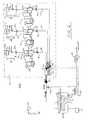
- FIG. 1Ais a simplified diagram of a chemical vapor deposition (“CVD”) system 100 according to the present invention.
- This systemis suitable for performing thermal, sub-atmospheric CVD (“SACVD”) processes, as well as other processes, such as reflow, drive-in, cleaning, etching, and gettering processes. Multiple-step processes can also be performed on a single substrate or wafer without removing the substrate from the chamber.
- the major components of the systeminclude, among others, a vacuum chamber 35 that receives process and other gases from a gas delivery system 31 , a vacuum system 112 , a remote microwave plasma system 155 , and a system controller 61 . These and other components are described below in order to understand the present invention.
- the CVD apparatus 100includes an enclosure assembly 201 housing a vacuum chamber 35 with a gas reaction area 21 .
- a gas distribution plate 106is provided above the central gas reaction area 21 for dispersing reactive gases and other gases, such as purge gases, through perforated holes in the gas distribution plate 106 to a wafer (not shown) that rests on a vertically movable heater 110 (also referred to as a wafer support pedestal).
- the heater 110can be controllably moved between a lower position, where a wafer can be loaded or unloaded, for example, and a processing position closely adjacent to the gas distribution plate 106 , indicated by a dashed line 113 , or to other positions for other purposes, such as for an etch or cleaning process.
- a center board(not shown) includes sensors for providing information on the position of the wafer.
- the heater 110includes an electrically resistive heating element (not shown) enclosed in a ceramic.
- the ceramicprotects the heating element from potentially corrosive chamber environments and allows the heater to attain temperatures up to about 600° C. or even higher.
- all surfaces of the heater 110 exposed to the vacuum chamber 35are made of a ceramic material, such as aluminum oxide (Al 2 O 3 or alumina) or aluminum nitride.
- Reactive and carrier gasesare supplied into a gas mixing manifold (also called a gas mixing box or block) 37 , where they are preferably mixed together and delivered to the gas distribution plate 106 .
- the gas mixing box 37may comprise a dual input mixing block coupled to a gas delivery system 31 and to a cleaning/etch gas conduit 147 .
- a valve 280operates to admit or seal gas or plasma from the gas conduit 147 to the gas mixing block 37 .
- the gas conduit 147receives gases from an integral remote microwave plasma system 155 , which has an inlet 157 for receiving input gases.
- gas supplied to the plate 106is vented toward the wafer surface where it may be uniformly distributed radially across the wafer surface, typically in a laminar flow.
- Purging gasmay be delivered into the vacuum chamber 35 from the plate 106 and/or an inlet port or tube (not shown in FIG. 1A) through the bottom wall of enclosure assembly 201 .
- the purging gasflows upward from the inlet port past the heater 110 and to an annular pumping channel 40 .
- An exhaust systemthen exhausts the gas (as indicated by arrows 22 ) into the annular pumping channel 40 and through an exhaust line 114 to a vacuum system 112 , which includes a vacuum pump (not shown). Exhaust gases and entrained particles are drawn from the annular pumping channel 40 through the exhaust line 114 at a rate controlled by a throttle valve system 63 .
- the remote microwave plasma system 155can produce a plasma for selected applications, such as chamber cleaning or etching native oxide or residue from a process wafer.
- Plasma species produced in the remote plasma system 155 from precursors supplied via the input line 157are sent via the conduit 147 for dispersion through the plate 106 to the vacuum chamber 35 .
- Precursor gases for a cleaning applicationmay include fluorine, chlorine, and other reactive elements.
- the remote microwave plasma system 155also may be adapted to deposit plasma-enhanced CVD films by selecting appropriate deposition precursor gases for use in the remote microwave plasma system 155 .
- the system controller 61controls activities and operating parameters of the deposition system.
- the processor 50executes system control software, such as a computer program stored in a memory 70 coupled to the processor 50 .
- the memory 70may be a hard disk drive, but of course the memory 70 may be other kinds of memory, such as read-only memory or flash memory.
- the CVD apparatus 100in a preferred embodiment includes a floppy disk drive and a card rack (not shown).
- the processor 50operates according to system control software, which includes sets of instructions that dictate the timing, mixture of gases, chamber pressure, chamber temperature, microwave power levels, susceptor position, and other parameters of a particular process.
- system control softwareincludes sets of instructions that dictate the timing, mixture of gases, chamber pressure, chamber temperature, microwave power levels, susceptor position, and other parameters of a particular process.
- Other computer programssuch as those stored on other memory including, for example, a floppy disk or another computer program product inserted in a disk drive or other appropriate drive, may also be used to operate the processor 50 to configure the CVD system 10 into various apparatus.
- the processor 50has a card rack (not shown) that contains a single-board computer, analog and digital input/output boards, interface boards and stepper motor controller boards.
- Various parts of the CVD system 100conform to the Versa Modular European (VME) standard which defines board, card cage, and connector dimensions and types.
- VMEVersa Modular European
- the VME standardalso defines the bus structure having a 16-bit data bus and 24-bit address bus.
- FIG. 1Bis a simplified diagram of a user interface in relation to the CVD apparatus chamber 35 .
- the CVD apparatus 100includes one chamber of a multichamber system. Wafers may be transferred from one chamber to another for additional processing. In some cases the wafers are transferred under vacuum or a selected gas.
- the interface between a user and the processoris via a CRT monitor 73 a and a light pen 73 b .
- a mainframe unit 75provides electrical, plumbing, and other support functions for the CVD apparatus 100 .
- Exemplary mainframe units compatible with the illustrative embodiment of the CVD apparatusare currently commercially available as the PRECISION 5000® and the CENTURA® 5200 systems from APPLIED MATERIALS, INC. of Santa Clara, Calif.
- two monitors 73 aare used, one mounted in the clean room wall 71 for the operators, and the other behind the wall 72 for the service technicians. Both monitors 73 a simultaneously display the same information, but only one light pen 73 b is enabled.
- the light pen 73 bdetects light emitted by the CRT display with a light sensor in the tip of the pen.
- the operatortouches a designated area of the display screen and pushes the button on the pen 73 b .
- the touched areachanges its highlighted color, or a new menu or screen is displayed, confirming communication between the light pen and the display screen.
- other devicessuch as a keyboard, mouse, or other pointing or communication device, may be used instead of or in addition to the light pen 73 b to allow the user to communicate with the processor.
- FIG. 1Cis an illustrative block diagram of the hierarchical control structure of the system control software, computer program 250 , according to a specific embodiment.
- a processes for depositing a film, performing a clean, or performing reflow or drive-incan be implemented using a computer program product that is executed by the processor 50 .
- the computer program codecan be written in any conventional computer readable programming language, such as 68000 assembly language, C, C++, Pascal, Fortran, or other language.
- Suitable program codeis entered into a single file, or multiple files, using a conventional text editor and is stored or embodied in a computer-usable medium, such as the system memory.
- the codeis compiled, and the resultant compiler code is then linked with an object code of precompiled WINDOWSTM library routines.
- the system userinvokes the object code, causing the computer system to load the code in memory, from which the CPU reads and executes code to configure the apparatus to perform tasks identified in the program.
- a userenters a process set number and process chamber number into a process selector subroutine 253 by using the light pen to select a choice provided by menus or screens displayed on the CRT monitor.
- the process setswhich are predetermined sets of process parameters necessary to carry out specified processes, are identified by predefined set numbers.
- the process selector subroutine 253identifies (i) the desired process chamber, and (ii) the desired set of process parameters needed to operate the process chamber for performing the desired process.
- the process parameters for performing a specific processrelate to process conditions such as, for example, process gas composition and flow rates, temperature, pressure, plasma conditions such as magnetron power levels (and alternatively to or in addition to high- and low-frequency RF power levels and the low-frequency RF frequency, for embodiments equipped with RF plasma systems), cooling gas pressure, and chamber wall temperature.
- the process selector subroutine 253controls what type of process (e.g. deposition, wafer cleaning, chamber cleaning, chamber gettering, reflowing) is performed at a certain time in the chamber. In some embodiments, there may be more than one process selector subroutine.
- the process parametersare provided to the user in the form of a recipe and may be entered utilizing the light pen/CRT monitor interface.
- a process sequencer subroutine 255has program code for accepting the identified process chamber and process parameters from the process selector subroutine 253 , and for controlling the operation of the various process chambers. Multiple users can enter process set numbers and process chamber numbers, or a single user can enter multiple process set numbers and process chamber numbers, so process sequencer subroutine 255 operates to schedule the selected processes in the desired sequence.
- the process sequencer subroutine 255includes program code to perform the steps of (i) monitoring the operation of the process chambers to determine if the chambers are being used, (ii) determining what processes are being carried out in the chambers being used, and (iii) executing the desired process based on availability of a process chamber and the type of process to be carried out.
- the process sequencer subroutine 255can be designed to take into consideration the present condition of the process chamber being used in comparison with the desired process conditions for a selected process, or the “age” of each particular user-entered request, or any other relevant factor a system programmer desires to include for determining scheduling priorities.
- the process sequencer subroutine 255determines which process chamber and process set combination is going to be executed next, the process sequencer subroutine 255 initiates execution of the process set by passing the particular process set parameters to a chamber manager subroutine 257 a - c which controls multiple processing tasks in the process chamber according to the process set determined by the process sequencer subroutine 255 .
- the chamber manager subroutine 257 ahas program code for controlling CVD and cleaning process operations in the process chamber.
- Chamber manager subroutine 257also controls execution of various chamber component subroutines which control operation of the chamber components necessary to carry out the selected process set.
- chamber component subroutinesare substrate positioning subroutine 260 , process gas control subroutine 263 , pressure control subroutine 265 , heater control subroutine 267 , plasma control subroutine 270 , endpoint detect control subroutine 259 , and gettering control subroutine 269 .
- the chamber manager subroutine 257 aselectively schedules or calls the process component subroutines in accordance with the particular process set being executed.
- the chamber manager subroutine 257 aschedules the process component subroutines much like the process sequencer subroutine 255 schedules which process chamber and process set are to be executed next.
- the chamber manager subroutine 257 aincludes monitoring various chamber components, determining which components need to be operated based on process parameters for the process set to be executed, and initiating execution of a chamber component subroutine responsive to the monitoring and determining steps.
- the substrate positioning subroutine 260comprises program code for controlling chamber components that are used to load the substrate onto the heater 110 and, optionally, to lift the substrate to a desired height in the chamber to control the spacing between the substrate and the gas distribution manifold 106 .
- the heater 110is lowered to receive the substrate and then the heater 110 is raised to the desired height.
- the substrate positioning subroutine 260controls movement of the heater 110 in response to process set parameters related to the support height that are transferred from the chamber manager subroutine 257 a.
- the process gas control subroutine 263has program code for controlling process gas composition and flow rates.
- the process gas control subroutine 263controls the state of safety shut-off valves, and also ramps the mass flow controllers up or down to obtain the desired gas flow rate.
- the process gas control subroutine 263operates by opening the gas supply lines and repeatedly (i) reading the necessary mass flow controllers, (ii) comparing the readings to the desired flow rates received from the chamber manager subroutine 257 a , and (iii) adjusting the flow rates of the gas supply lines as necessary.
- the process gas control subroutine 263includes steps for monitoring the gas flow rates for unsafe rates, and activating the safety shut-off valves when a fault or an unsafe condition is detected.
- Alternative embodimentscould have more than one process gas control subroutine, each subroutine controlling a specific type of process or specific sets of gas lines.
- an inert gassuch as nitrogen or argon
- process gas control subroutine 263is programmed to include steps for flowing the inert gas into the chamber for an amount of time necessary to stabilize the pressure in the chamber, and then the steps described above would be carried out.
- process gas control subroutine 263when a process gas is to be vaporized from a liquid precursor, such as TEOS, process gas control subroutine 263 would be written to include steps for bubbling a delivery gas such as helium through the liquid precursor in a bubbler assembly, or controlling a liquid injection system to spray or squirt liquid into a stream of carrier gas, such as helium, through the LFM.
- a delivery gassuch as helium
- the process gas control subroutine 263regulates the flow of the delivery gas, the pressure in the bubbler, and the bubbler temperature in order to obtain the desired process gas flow rates.
- the desired process gas flow ratesare transferred to the process gas control subroutine 263 as process parameters.
- the process gas control subroutine 263includes steps for obtaining the necessary delivery gas flow rate, bubbler pressure, and bubbler temperature for the desired process gas flow rate by accessing a stored table containing the necessary values for a given process gas flow rate. Once the necessary values are obtained, the delivery gas flow rate, bubbler pressure and bubbler temperature are monitored, compared to the necessary values and adjusted accordingly.
- the process gas control subroutine 263also includes steps for detecting clogging of components of the gas delivery system, and for alerting the operator or shutting down the system in the event of clogging.
- clogging of an injection valve or other component of the gas delivery systemmay be indicated by an elevated pressure upstream of the mass flow controller that provides a flow of gas to the injection valve.
- the pressure upstream of the mass flow controllercan be monitored by the process gas control subroutine, with a fault indicated or system shut-down initiated where the pressure parameters reveal clogging of the line or valve.
- the pressure control subroutine 265comprises program code for controlling the pressure in the chamber by regulating the aperture size of the throttle valve in the exhaust system of the chamber.
- the aperture size of the throttle valveis set to control the chamber pressure at a desired level in relation to the total process gas flow, the size of the process chamber, and the pumping set-point pressure for the exhaust system.
- the desired or target pressure levelis received as a parameter from the chamber manager subroutine 257 a .
- the pressure control subroutine 265measures the pressure in the chamber by reading one or more conventional pressure manometers connected to the chamber, compares the measure value(s) to the target pressure, obtains proportional, integral, and differential (“PID”) values corresponding to the target pressure from a stored pressure table, and adjusts the throttle valve according to the PID values.
- PIDproportional, integral, and differential
- the pressure control subroutine 265can be written to open or close the throttle valve to a particular aperture size, i.e. a fixed position, to regulate the pressure in the chamber. Controlling the exhaust capacity in this way does not invoke the feedback control feature of the pressure control subroutine 265 .
- the heater control subroutine 267comprises program code for controlling the current to a heating unit that is used to heat the substrate.
- the heater control subroutine 267is also invoked by the chamber manager subroutine 257 a and receives a target, or set-point, temperature parameter.
- the heater control subroutine 267measures the temperature by measuring voltage output of a thermocouple located in the heater, comparing the measured temperature to the set-point temperature, and increasing or decreasing current applied to the heating unit to obtain the set-point temperature.
- the temperatureis obtained from the measured voltage by looking up the corresponding temperature in a stored conversion table, or by calculating the temperature using a fourth-order polynomial.
- the heater control subroutine 267includes the ability to gradually control a ramp up or down of the heater temperature. This feature helps to reduce thermal cracking in the ceramic heater. Additionally, a built-in fail-safe mode can be included to detect process safety compliance, and can shut down operation of the heating unit if the process chamber is not properly set up.
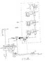
- FIG. 2is a schematic diagram of an embodiment of a chemical vapor deposition (CVD) system 100 including a gas delivery system 31 in accordance with the present invention.
- Gas delivery system 31is in fluid communication with processing chamber 35 through mixing manifold 37 .
- the processing chamber 35is a CVD chamber configured to deposit silicon dioxide by flowing vaporized TEPO, tetraethyl orthosilicate (TEOS), and tetraethyl borate (TEB) into the processing chamber 35 .
- TEPOtetraethyl orthosilicate
- TEBtetraethyl borate
- embodiments in accordance with the present inventionare not limited to this specific application, and may include one, two, four, or an even greater number of separate, devoted lines for delivering a variety of gases and vaporized liquids.
- Chemical vapor deposition (CVD) system 100generally includes a chamber 35 , a chamber lid 104 having a gas distributor 106 , with the gas delivery system 31 fluidly connected to gas distributor 106 to deliver one or more processing gases into chamber 35 .
- a substrate support member 110is disposed in the chamber.
- a vacuum exhaust system 112is connected to a gas outlet or foreline 114 of the chamber, and a system controller 61 is connected to control operation of the CVD system.
- Specific examples of CVD systems utilizing gas delivery apparatuses and methods in accordance with embodiments of the present inventioninclude the Ultima HDP-CVDTM chamber/system and the DXZTM chamber/system, which are available from Applied Materials, Inc. of Santa Clara, Calif.
- the substrate support member 110is typically made of a ceramic or aluminum nitride (AlN) and may include a heater such as a resistive heating coil disposed inside the substrate support member, and may also include substrate chucking mechanisms for securely holding a substrate, such as a vacuum chuck or an electrostatic chuck.
- the gas distributor 106may comprise a showerhead type gas distributor or a plurality of injection nozzles, for providing a uniform process gas distribution over a substrate disposed on the substrate support member 110 .
- a temperature control systemsuch as a resistive heating coil and/or thermal fluid channels, may be disposed in thermal connection with the lid and the gas distributor 106 . The temperature control system maintains the temperature of the gas distributor 106 within a desired range throughout processing. While gas distributor 106 is fluidly connected to the gas delivery system 31 , gas distributor 106 may also be fluidly connected to one or more additional gas sources 120 through one or more additional mass flow controllers 122 .
- the exhaust system 112includes one or more vacuum pumps 124 , such as a turbomolecular pump, connected to exhaust gases from and maintain vacuum levels in the chamber 102 .
- the one or more vacuum pumps 124are connected to the foreline 114 for exhausting gases through a valve such as a gate valve.
- One or more cold traps 126may be disposed on foreline 114 to remove or condense particular gases exhausted from the chamber.
- Gas delivery system 31comprises three processing liquid vaporization stages 10 a - c in fluid communication with processing chamber 35 through devoted delivery lines 88 a - c respectively.
- First stage 10 acomprises a first injection valve 11 a coupled to a source of liquid TEB 25 a via a first liquid flow meter 23 a .
- Second stage 10 bcomprises a second injection valve 11 b coupled to a source of liquid TEOS 25 b via a second liquid flow meter 23 b .
- Third stage 10 ccomprises a third injection valve 11 c coupled to a source of liquid TEPO 25 c via a third liquid flow meter 23 c.
- Each source of processing liquid 25 a - cis coupled to a respective source of pressurized helium 29 a - c.
- the gas delivery system of FIG. 2supplies carrier gas to each vaporization stage from separate carrier gas sources 33 a - c through carrier gas delivery lines controlled by separate mass flow controllers (MFCs) 39 a - c respectively.
- MFCsmass flow controllers
- Each mass flow controlleris in communication with system controller 61 , allowing for control over the mass flow controller.
- N 2constant for units
- G ggas specific gravity
- T uabsolute upstream pressure
- Equation (I)Certain variables of equation (I) are constant under typical operating conditions.
- the flow rate (q) of the carrier gasmay be maintained constant by the mass flow controller, and the downstream pressure at the process chamber (pd) may be maintained constant by the throttle valve.
- the N 2 , G g and T u variables of Equation (I)may also be constant.
- clogging of any injection valvewill cause the flow coefficient (C v ) to fall and the upstream pressure (p u ) to rise.
- p uthe upstream pressure
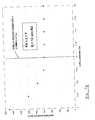
- FIGS. 7A and 7BCorrelation between clogging of an injection valve and an increase in pressure is shown in FIGS. 7A and 7B, which plot pressure upstream of an injection valve versus the diameter of the orifice in the injection valve through which gas is flowed.
- FIG. 7Aplots the correlation between upstream pressure and orifice diameter for nitrogen gas flowed at a rate of 12 slm into a chamber having a downstream pressure of 3.7 Torr.
- FIG. 7Bplots the correlation between upstream pressure and orifice diameter for helium gas flowed at a rate of 12 slm into a chamber having a downstream pressure of 200 Torr. Both figures reflect an exponential increase in p u where the diameter of the orifice falls below a minimum.
- Embodiments of the present inventionaccordingly exploit this relationship between upstream pressure and effective orifice diameter in order to reveal clogging.
- pressure transducers 99 a - care positioned on delivery lines 88 a - c , between mass flow controllers 39 a - c and injection valves 15 a - c , respectively.
- transducer typeswhich may be relied upon to detect clogging in accordance with embodiments of the present invention.
- One exampleis the family of BARATRON® type 740 and 750 industrial pressure transducers manufactured by MKS Instruments, Inc., of Andover, Mass.
- Pressure transducers 99 a - care in communication with controller 61 to provide data regarding possible clogging of the injection valves positioned downstream.
- memory 50 of controller 61may include a computer-readable program embodied therein for receiving readings from the pressure transducers, and for comparing the readings to previously established pressure set point values.
- the computer-readable programmay include computer instructions for comparing a pressure upstream of one of the mass flow controllers relative to a setpoint pressure, and also include instructions for automatically alerting an operator to a possible fault and/or halting operation of the apparatus when the pressure upstream of the first or second mass flow controllers deviates by a predetermined amount from the setpoint pressure, indicating possible obstruction of an orifice in the injection valve and clogging of the vaporization stage.
- the carrier gas flowed from devoted carrier gas sources 33 a - cvaporizes processing liquid within stages 10 a - c of gas delivery system 31 , respectively.
- Flow into and out of vaporization stages 10 a - cis controlled by valves positioned on the gas delivery lines both upstream and downstream of the vaporization stages.
- upstream shut off valves 89 a - ccontrol the flow of carrier gas through lines 88 a - c to vaporization stages 10 a - c , respectively.
- Final valves 90 a - c positioned downstream from vaporization stages 10 a - c respectively,govern the flow of the carrier gas/vaporized liquid mixture from vaporization stages 10 a - c to the mixing manifold 37 .
- an inert carrier gassuch as helium flows from the gas sources 33 a - c into flow controllers 39 a - c respectively, and the flow controllers 39 a - c are set at a first flow rate.
- the processing liquidis vaporized as described below in conjunction with FIG. 3.
- a mixture of vaporized TEB and heliumflows from outlet 17 a of the first injection valve 11 a through final valve 90 a and divert valve 91 a to the mixing manifold 37 .
- a mixture of vaporized TEOS and heliumflows from outlet 17 b of the second injection valve 11 b through final valve 90 b and divert valve 91 b to the mixing manifold 37 , and a mixture of vaporized TEPO and helium flows from outlet 17 c of the third injection valve 11 c through final valve 90 c and divert valve 91 c to the mixing manifold 37 .
- POU filter 200point-of-use filter 200 . While not limited to any particular pore size or manufacturer, an example of a filter utilized in this particular application is the 0.003 ⁇ m pore filter manufactured for semiconductor fabrication applications by Millipore of Bedford, Mass.
- the filtered mixturethen flows to the processing chamber 35 where the chamber pressure and temperature causes the TEB, TEOS and TEPO to react to form a doped silicon dioxide layer on a substrate (not shown) positioned within the processing chamber 35 .
- Divert valve 202is positioned immediately downstream of point-of-use filter 200 . Activation of divert valve 202 shunts the mixture of processing components into foreline 114 and away from processing chamber 35 for disposal.
- FIG. 3is a diagrammatic side elevational view of a generic vaporization stage 10 of the gas distribution apparatus 31 shown in FIG. 2.
- Vaporization stage 10comprises a conventional injection valve 11 that comprises a processing liquid inlet 13 for inputting a processing liquid, a carrier gas inlet 15 for inputting an inert carrier gas, and an outlet 17 for outputting a vaporized processing liquid/carrier gas mixture.
- the processing liquid inlet 13terminates at an orifice 19 leading to a central gas reaction area 21 where the processing liquid inlet 13 , the carrier gas inlet 15 , and the outlet 17 meet.
- the injection valve 11is configured such that the relative sizes of the orifice 19 and the central region 21 , and the pressures, flow rates and relative direction of the processing liquid and carrier gas flow cause a pressure drop within the central region 21 , as is conventionally known in the art.
- This pressure dropcauses processing liquid supplied to the processing liquid inlet 13 to vaporize as it passes from the processing liquid inlet 13 , through the orifice 19 to the central region 21 .
- the orifice 19is small, and thus may be vulnerable to clogging by generated residual generated solid material.
- the processing liquid inlet 13is coupled to a liquid flow meter (LFM) 23 of the vaporization stage 10 which controls the flow rate of processing liquid traveling to the injection valve 11 .
- the liquid flow meter 23also is coupled via line 27 to a source of processing liquid 25 within the vaporization stage 10 , which in turn is coupled to a source of pressurized helium 29 .
- the pressurized helium flowforces the processing liquid from the processing liquid source 25 through line 27 to the liquid flow meter 23 .
- the liquid flow meter 23controls the flow rate of the processing liquid as it travels from liquid flow meter 23 through the processing liquid inlet 13 and the orifice 19 to the central region 21 of the injection valve 11 .
- the processing liquidvaporizes and mixes with the carrier gas as the processing liquid enters the central region 21 , due to the pressure decrease experienced as the processing liquid travels from the orifice 19 to the central region 21 .
- the combined vaporized processing liquid/carrier gasflows from the injection valve 11 via the outlet 17 .
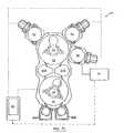
- FIG. 4is a top plan view of an automated tool 43 for fabricating semiconductor devices.
- the tool 43comprises a pair of load locks 45 a , 45 b , and a first wafer handler chamber 47 containing a first wafer handler 49 .
- the first wafer handler chamber 47is operatively coupled to the pair of load locks 45 a , 45 b and to a pair of pass-through chambers 51 a , 51 b .
- the pair of pass-through chambers 51 a , 51 bare further coupled to a second wafer handler chamber 53 (e.g., a transfer chamber), containing a second wafer handler 55 , and to a plurality of processing chambers 57 , 59 .
- the second wafer handler chamber 53is coupled to the processing chamber 35 of FIG. 1 which is further coupled to the inventive gas delivery system 31 .
- controller 61which comprises a microprocessor and a memory not shown in FIG. 4 having a program therein, which controls semiconductor wafer transfer among the load locks 45 a , 45 b , the pass-through chambers 51 a, 51 b, and the processing chambers 57 , 59 , 35 , and which controls processing therein.
- controller 61is also in communication with various components of the gas delivery system 31 , including mass flow controllers 39 a - c , pressure sensors 99 a - c , final valves 90 a - c , and diversion valves 91 a - c.
- the controller program and the overall configuration of the tool 43is designed for optimal productivity.
- a clogged gas delivery system within such a toolis particularly costly, as it can affect the productivity of the entire tool 43 , including the plurality of processing chambers contained therein.
- the value of the automated semiconductor processing tool 43increases significantly.
- Embodiments of methods and systems in accordance with the present inventionoffer a number of advantages over conventional liquid vaporization gas delivery techniques.
- One advantageis rapid and reliable detection of clogging of injection valves.
- conventional gas delivery techniquestypically utilize ex situ means for monitoring injection valves for clogging.
- the thickness of a deposited layeris measured and compared with expected values.
- a reduction in the thickness of the deposited layermay reveal a reduced flow of a vaporized liquid precursor material, and hence partial or complete obstruction or clogging of an injection valve.
- Such detection of clogging after-the-factis relatively expensive, as batches of wafers already processed and bearing the deposited layer of diminished thickness must be discarded.
- embodiments in accordance with the present inventionutilize real-time monitoring of pressures to allow detection of the clogging of injection valves in-situ.
- pressure monitoring techniquesallow rapid detection of clogging, such that at a minimum only the wafers actually being processed during the clogging event are affected and need to be scrapped before the situation is corrected.
- rapidity and precision of the indication of cloggingmay allow the tool operator to take corrective action and thereby prevent even those wafers being processed from falling outside the specified tolerance range.
- the present inventionmay reduce clogging within any processing environment wherein mixed processing constituents may react to form an undesirable product that can clog the various components within a gas delivery system.
- liquid processing materialswhich may be vaporized prior to processing in the fabrication of semiconductors include, but are not limited to, titanium tetrachloride (TiCl 4 ), trimethylsilane (SiH(CH 3 ) 3 ), tetramethylsilane (Si(CH 3 ) 4 ), tetramethylcyclotetrasiloxane (TOMCATS), dimethyldimethoxysilane (Z 2 DM), trimethyl phosphite (TMPI), trimethylphosphate (TMPO), trimethylborate (TMB), phosphorus oxychloride (POCl 3 ), boron tribromide (BBr 3 ), bis(tertiary-butylamino)silane (BTBAS), tantalum pentaethoxide (TAETO), tantalum tetraethoxide dimethylaminoethoxide (TAT-DMAE), tert-butylimino tris(diethylamino) tantalum (
- FIG. 5shows a simplified schematic view of a first alternative embodiment of a chemical vapor deposition (CVD) system 500 including a gas delivery system 531 in accordance with the present invention, wherein a single carrier gas source 533 supplies a flow of carrier gas to three injection valves 511 a - c arranged in parallel along branches 598 a - c of carrier gas flow line 588 . Clogging of any one of the three injection valves 511 a - c may be detected by monitoring the pressure indicated by the single pressure transducer 599 .
- CVDchemical vapor deposition
- the setpoint of transducer 599may be based upon unobstructed flow through each of the parallel injection valves, with an increase in detected pressure revealing a potential clogging event in any one of the injection valves.
- the embodiment shown in FIG. 5does not necessarily allow for precise identification of the particular valve which is experiencing clogging.
- the embodiment of FIG. 5may be advantageous because it requires purchase, maintenance, and monitoring of only a single carrier gas source, mass flow controller, and pressure transducer, and may readily be adapted for use with existing gas delivery systems having the disclosed configuration.
- FIG. 6shows a simplified schematic view of a second alternative embodiment of a chemical vapor deposition (CVD) system 600 including a gas delivery system 631 in accordance with the present invention, wherein single pressure transducer 699 is positioned on carrier gas flow line 688 between mass flow controller 639 and three serially-arranged injection valves 611 a - c . Clogging of any one of the three serial injection valves 611 a - c may be detected by monitoring the pressure indicated by transducer 699 .
- CVDchemical vapor deposition
- the setpoint of transducer 699is based upon unobstructed flow through the entire series of three injection valves, with an increase in detected pressure revealing a potential clogging event in one of the valves.
- this embodimentmay be advantageous because it requires the purchase, maintenance, and monitoring of only a single carrier gas source, mass flow controller, and pressure transducer, and may readily be adapted for use with existing gas delivery systems having the disclosed configuration.
- the exemplary gas delivery systemmay contain additional components (e.g., valves, flow meters, etc.), and the various components of the gas delivery system can be made with reduced nickel content and increased chromium content to further reduce formation of residues. And although the benefits of the inventive gas delivery system are most dramatic when used with injection valves, other vaporization mechanisms such as bubblers may also be employed.
- gas panel components of systems and methods in accordance with embodiments of the present inventionmay take the form of assemblies of discrete lines, valves, inlets, outlet, and transducers.
- gas panels utilized in accordance with embodiments of the present inventionmay be formed from integral blocks having flow lines, chambers, inlets, outlets, and other ports formed therein by machining or other fabrication methods.
Landscapes
- Chemical & Material Sciences (AREA)
- General Chemical & Material Sciences (AREA)
- Chemical Kinetics & Catalysis (AREA)
- Engineering & Computer Science (AREA)
- Materials Engineering (AREA)
- Mechanical Engineering (AREA)
- Metallurgy (AREA)
- Organic Chemistry (AREA)
- Chemical Vapour Deposition (AREA)
Abstract
Description
- Chemical vapor deposition (CVD) and other processing employed in the fabrication of semiconductor devices may utilize a number of gases. These gases, which may take the form of vaporized liquid precursors, are generated and supplied to a CVD chamber via a system of pipes or lines and vaporizing mechanisms known as a gas delivery system. Typically a separate vaporizing mechanism is provided for vaporizing each processing liquid precursor, and is coupled to a source of processing liquid and a source of carrier gas. Each vaporizing mechanism and processing liquid source combination within a gas delivery system is referred to as a vaporization stage. Although a number of vaporizing mechanisms exist (e.g., bubblers, injection valves, etc.), most conventional gas delivery systems employ a plurality of injection valves for vaporizing processing liquids that are to be delivered to a CVD chamber.[0001]
- A typical injection valve comprises a processing liquid inlet for receiving a pressurized processing liquid, a carrier gas inlet for receiving a pressurized inert carrier gas, and an outlet for delivering a vaporized processing liquid/carrier gas mixture. The injection valve is heated such that when the processing liquid is injected into the carrier gas, the heat and the low partial vapor pressure of the processing liquid in the carrier gas causes the processing liquid to vaporize. A high carrier gas pressure produces more processing liquid vaporization by lowering the partial vapor pressure of the processing liquid within the carrier gas. Accordingly, when designing a gas delivery system, maintenance of adequate carrier gas pressure is an important consideration, as is minimizing overall system size and complexity.[0002]
- To achieve a low partial vapor pressure for each processing precursor liquid while minimizing system size, conventional gas delivery systems are configured such that a carrier gas is delivered (via a mass flow controller) to a first injection valve, where it is used to vaporize a first processing liquid, forming a first vaporized processing liquid/carrier gas mixture. Where a second liquid precursor is also utilized in processing, the first vaporized processing liquid/carrier gas mixture may then be delivered in serial to the carrier gas inlet of a second, consecutive injection valve used to vaporize a second processing liquid. Where additional liquid precursors are also employed in processing, a mixture of the first and second vaporized processing liquids and the carrier gas is then delivered in serial to the carrier gas inlet of a third consecutive injection valve, etc.[0003]
- The gas delivery system configurations just described provide a compact and cost-effective system, as they employ a single gas line and a single carrier gas source controlled by a single mass flow controller to achieve vaporization within each of the various vaporization stages. Additionally, conventional gas delivery systems facilitate vaporization of liquid precursors, as the entire mass flow of the carrier gas is applied to each injection valve in the series.[0004]
- Despite their overall compact and efficient design, the maintenance and proper operation of conventional gas delivery systems may be expensive. For example, the orifices in the injection valve through which the carrier gas flows and through which the liquid precursor flows are narrow and prone to clogging. Solid material which can obstruct these narrow passageways in the injection valve may result from the presence of impurities or moisture in the metal tubing, liquid precursor, or carrier gas.[0005]
- Unfortunately, conventional gas delivery systems do not include a sensor warning of clogging of the injection valve. Instead, clogging of an injection valve is generally detectable only indirectly, by observation of defects in wafers resulting from incomplete exposure to the vaporized liquid precursor, which has been blocked by the obstructed injection valve. This after-the-fact indication of injection valve clogging can be expensive, as entire lots of processed wafers may need to be scrapped.[0006]
- Accordingly, a need exists for a gas delivery system for a semiconductor processing tool which allows for the rapid and effective detection of clogging of an injection valve.[0007]
- Early detection of clogging of a liquid precursor injection valve in a semiconductor fabrication tool is permitted through monitoring of pressure upstream of the valve. The increase in pressure associated with obstruction of the valve may trigger alarms which alert the operator and allow rapid correction of the problem, before substantial numbers of wafers are improperly processed utilizing the clogged valve.[0008]
- A embodiment of a system in accordance with the present invention for providing a vaporized liquid precursor to a semiconductor processing chamber, comprises, a mass flow controller in fluid communication with a pressurized carrier gas source through a carrier gas flow line. A liquid precursor injection valve is in fluid communication with the mass flow controller through the carrier gas flow line, in fluid communication with a liquid precursor source through a first line, and in fluid communication with a processing chamber through a delivery line. A pressure transducer is in communication with the carrier gas flow line and configured to detect a pressure within the carrier gas flow line between the mass flow controller and the injection valve.[0009]
- An embodiment of an apparatus in accordance with the present invention for processing a semiconductor substrate, comprises, a processing chamber comprising a chamber lid and walls enclosing a substrate support, a gas distributor, and a vacuum exhaust connected to a chamber outlet. A gas delivery system is in fluid communication with the gas distributor, the gas delivery system comprising a mass flow controller in fluid communication with a pressurized carrier gas source through a carrier gas flow line. The gas delivery system also comprises a liquid precursor injection valve in fluid communication with the mass flow controller through the carrier gas flow line, in fluid communication with a liquid precursor source through a first line, and in fluid communication with a processing chamber through a delivery line. The gas delivery system further comprises a pressure transducer in communication with the carrier gas flow line and configured to detect a pressure within the carrier gas flow line between the mass flow controller and the injection valve. The apparatus further comprises a system controller comprises a memory and a processor, the processor in electrical communication with the pressure transducer.[0010]
- An embodiment of method in accordance with the present invention for detecting clogging of an injection valve providing vaporized liquid precursor material to a semiconductor processing chamber, comprises, detecting a pressure at a point between the injection valve and a mass flow controller providing a carrier gas to the injection valve.[0011]
- An embodiment of a vaporizing system in accordance with the present invention comprises a liquid injection valve having first and second inlets and an outlet, the injection valve capable of receiving a carrier gas at the first inlet, receiving a liquid precursor at the second inlet, and delivering a mixture of vaporized liquid precursor and carrier gas through the outlet. The vaporizing system further comprises a carrier gas source, a first gas line that couples the carrier gas source to the first inlet, a liquid precursor source, and a second gas line that couples the liquid precursor source to the second inlet. A mass flow controller is operatively coupled to the first gas line. A pressure transducer is coupled to the first gas line between the mass flow controller and the first inlet.[0012]
- A method of delivering vaporized liquid to a processing chamber comprises separately flowing a carrier gas and a liquid to an injection valve. The liquid is vaporized with the injection valve and the vaporized liquid is combined with the carrier gas. Pressure of the carrier gas upstream of the injection valve is detected, and detected pressure is compared versus a setpoint pressure value.[0013]
- These and other embodiments of the present invention, as well as its advantages and features, are described in more detail in conjunction with the text below and attached figures.[0014]
- FIG. 1A is a simplified representation of a CVD apparatus according to the present invention.[0015]
- FIG. 1B is a simplified representation of the user interface for a CVD system in relation to a deposition chamber in a multi-chamber system.[0016]
- FIG. 1C is a simplified of a block diagram of the hierarchical control structure of the system control software according to a specific embodiment.[0017]
- FIG. 2 is a schematic diagram of a chemical vapor deposition system including one embodiment of a gas delivery system in accordance with the present invention.[0018]
- FIG. 3 is a diagrammatic side elevational view of a generic vaporization stage comprising a conventional injection valve useful in describing the preferred embodiment of the invention.[0019]
- FIG. 4 is a top plan view of an automated tool for semiconductor device fabrication which employs the gas delivery system of FIG. 2.[0020]
- FIG. 5 is a schematic diagram of a chemical vapor deposition system including a first alternative embodiment of a gas delivery system in accordance with the present invention.[0021]
- FIG. 6 is a schematic diagram of a chemical vapor deposition system including a second alternative embodiment of a gas delivery system in accordance with the present invention.[0022]
- FIGS. 7A and 7B plot pressure upstream of an injection valve versus diameter of the orifice through which gas is flowed, for two different conditions of gas flow.[0023]
- I. Exemplary Deposition System[0024]
- FIG. 1A is a simplified diagram of a chemical vapor deposition (“CVD”)[0025]
system 100 according to the present invention. This system is suitable for performing thermal, sub-atmospheric CVD (“SACVD”) processes, as well as other processes, such as reflow, drive-in, cleaning, etching, and gettering processes. Multiple-step processes can also be performed on a single substrate or wafer without removing the substrate from the chamber. The major components of the system include, among others, avacuum chamber 35 that receives process and other gases from agas delivery system 31, avacuum system 112, a remote microwave plasma system155, and asystem controller 61. These and other components are described below in order to understand the present invention. - The[0026]
CVD apparatus 100 includes anenclosure assembly 201 housing avacuum chamber 35 with agas reaction area 21. Agas distribution plate 106 is provided above the centralgas reaction area 21 for dispersing reactive gases and other gases, such as purge gases, through perforated holes in thegas distribution plate 106 to a wafer (not shown) that rests on a vertically movable heater110 (also referred to as a wafer support pedestal). Theheater 110 can be controllably moved between a lower position, where a wafer can be loaded or unloaded, for example, and a processing position closely adjacent to thegas distribution plate 106, indicated by a dashedline 113, or to other positions for other purposes, such as for an etch or cleaning process. A center board (not shown) includes sensors for providing information on the position of the wafer. - The[0027]
heater 110 includes an electrically resistive heating element (not shown) enclosed in a ceramic. The ceramic protects the heating element from potentially corrosive chamber environments and allows the heater to attain temperatures up to about 600° C. or even higher. In an exemplary embodiment, all surfaces of theheater 110 exposed to thevacuum chamber 35 are made of a ceramic material, such as aluminum oxide (Al2O3or alumina) or aluminum nitride. - Reactive and carrier gases are supplied into a gas mixing manifold (also called a gas mixing box or block)[0028]37, where they are preferably mixed together and delivered to the
gas distribution plate 106. Thegas mixing box 37 may comprise a dual input mixing block coupled to agas delivery system 31 and to a cleaning/etch gas conduit 147. Avalve 280 operates to admit or seal gas or plasma from thegas conduit 147 to thegas mixing block 37. Thegas conduit 147 receives gases from an integral remote microwave plasma system155, which has aninlet 157 for receiving input gases. During deposition processing, gas supplied to theplate 106 is vented toward the wafer surface where it may be uniformly distributed radially across the wafer surface, typically in a laminar flow. - Purging gas may be delivered into the[0029]
vacuum chamber 35 from theplate 106 and/or an inlet port or tube (not shown in FIG. 1A) through the bottom wall ofenclosure assembly 201. The purging gas flows upward from the inlet port past theheater 110 and to anannular pumping channel 40. An exhaust system then exhausts the gas (as indicated by arrows22) into theannular pumping channel 40 and through anexhaust line 114 to avacuum system 112, which includes a vacuum pump (not shown). Exhaust gases and entrained particles are drawn from theannular pumping channel 40 through theexhaust line 114 at a rate controlled by athrottle valve system 63. - The remote microwave plasma system[0030]155 can produce a plasma for selected applications, such as chamber cleaning or etching native oxide or residue from a process wafer. Plasma species produced in the remote plasma system155 from precursors supplied via the
input line 157 are sent via theconduit 147 for dispersion through theplate 106 to thevacuum chamber 35. Precursor gases for a cleaning application may include fluorine, chlorine, and other reactive elements. The remote microwave plasma system155 also may be adapted to deposit plasma-enhanced CVD films by selecting appropriate deposition precursor gases for use in the remote microwave plasma system155. - The[0031]
system controller 61 controls activities and operating parameters of the deposition system. Theprocessor 50 executes system control software, such as a computer program stored in amemory 70 coupled to theprocessor 50. Preferably, thememory 70 may be a hard disk drive, but of course thememory 70 may be other kinds of memory, such as read-only memory or flash memory. In addition to a hard disk drive (e.g., memory70), theCVD apparatus 100 in a preferred embodiment includes a floppy disk drive and a card rack (not shown). - The[0032]
processor 50 operates according to system control software, which includes sets of instructions that dictate the timing, mixture of gases, chamber pressure, chamber temperature, microwave power levels, susceptor position, and other parameters of a particular process. Other computer programs such as those stored on other memory including, for example, a floppy disk or another computer program product inserted in a disk drive or other appropriate drive, may also be used to operate theprocessor 50 to configure theCVD system 10 into various apparatus. - The[0033]
processor 50 has a card rack (not shown) that contains a single-board computer, analog and digital input/output boards, interface boards and stepper motor controller boards. Various parts of theCVD system 100 conform to the Versa Modular European (VME) standard which defines board, card cage, and connector dimensions and types. The VME standard also defines the bus structure having a 16-bit data bus and 24-bit address bus. - FIG. 1B is a simplified diagram of a user interface in relation to the[0034]
CVD apparatus chamber 35. TheCVD apparatus 100 includes one chamber of a multichamber system. Wafers may be transferred from one chamber to another for additional processing. In some cases the wafers are transferred under vacuum or a selected gas. The interface between a user and the processor is via aCRT monitor 73aand alight pen 73b. Amainframe unit 75 provides electrical, plumbing, and other support functions for theCVD apparatus 100. Exemplary mainframe units compatible with the illustrative embodiment of the CVD apparatus are currently commercially available as the PRECISION 5000® and the CENTURA® 5200 systems from APPLIED MATERIALS, INC. of Santa Clara, Calif. - In the preferred embodiment two[0035]
monitors 73aare used, one mounted in theclean room wall 71 for the operators, and the other behind thewall 72 for the service technicians. Both monitors73asimultaneously display the same information, but only onelight pen 73bis enabled. Thelight pen 73bdetects light emitted by the CRT display with a light sensor in the tip of the pen. To select a particular screen or function, the operator touches a designated area of the display screen and pushes the button on thepen 73b. The touched area changes its highlighted color, or a new menu or screen is displayed, confirming communication between the light pen and the display screen. Of course, other devices, such as a keyboard, mouse, or other pointing or communication device, may be used instead of or in addition to thelight pen 73bto allow the user to communicate with the processor. - FIG. 1C is an illustrative block diagram of the hierarchical control structure of the system control software,[0036]
computer program 250, according to a specific embodiment. A processes for depositing a film, performing a clean, or performing reflow or drive-in can be implemented using a computer program product that is executed by theprocessor 50. The computer program code can be written in any conventional computer readable programming language, such as 68000 assembly language, C, C++, Pascal, Fortran, or other language. - Suitable program code is entered into a single file, or multiple files, using a conventional text editor and is stored or embodied in a computer-usable medium, such as the system memory.[0037]
- If the entered code text is in a high-level language, the code is compiled, and the resultant compiler code is then linked with an object code of precompiled WINDOWS™ library routines. To execute the linked compiled object code, the system user invokes the object code, causing the computer system to load the code in memory, from which the CPU reads and executes code to configure the apparatus to perform tasks identified in the program.[0038]
- A user enters a process set number and process chamber number into a[0039]
process selector subroutine 253 by using the light pen to select a choice provided by menus or screens displayed on the CRT monitor. The process sets, which are predetermined sets of process parameters necessary to carry out specified processes, are identified by predefined set numbers. Theprocess selector subroutine 253 identifies (i) the desired process chamber, and (ii) the desired set of process parameters needed to operate the process chamber for performing the desired process. The process parameters for performing a specific process relate to process conditions such as, for example, process gas composition and flow rates, temperature, pressure, plasma conditions such as magnetron power levels (and alternatively to or in addition to high- and low-frequency RF power levels and the low-frequency RF frequency, for embodiments equipped with RF plasma systems), cooling gas pressure, and chamber wall temperature. Theprocess selector subroutine 253 controls what type of process (e.g. deposition, wafer cleaning, chamber cleaning, chamber gettering, reflowing) is performed at a certain time in the chamber. In some embodiments, there may be more than one process selector subroutine. The process parameters are provided to the user in the form of a recipe and may be entered utilizing the light pen/CRT monitor interface. - A[0040]
process sequencer subroutine 255 has program code for accepting the identified process chamber and process parameters from theprocess selector subroutine 253, and for controlling the operation of the various process chambers. Multiple users can enter process set numbers and process chamber numbers, or a single user can enter multiple process set numbers and process chamber numbers, soprocess sequencer subroutine 255 operates to schedule the selected processes in the desired sequence. Preferably, theprocess sequencer subroutine 255 includes program code to perform the steps of (i) monitoring the operation of the process chambers to determine if the chambers are being used, (ii) determining what processes are being carried out in the chambers being used, and (iii) executing the desired process based on availability of a process chamber and the type of process to be carried out. - Conventional methods of monitoring the process chambers, such as polling methods, can be used. When scheduling which process is to be executed, the[0041]
process sequencer subroutine 255 can be designed to take into consideration the present condition of the process chamber being used in comparison with the desired process conditions for a selected process, or the “age” of each particular user-entered request, or any other relevant factor a system programmer desires to include for determining scheduling priorities. - Once the[0042]
process sequencer subroutine 255 determines which process chamber and process set combination is going to be executed next, theprocess sequencer subroutine 255 initiates execution of the process set by passing the particular process set parameters to a chamber manager subroutine257a-cwhich controls multiple processing tasks in the process chamber according to the process set determined by theprocess sequencer subroutine 255. For example, thechamber manager subroutine 257ahas program code for controlling CVD and cleaning process operations in the process chamber. Chamber manager subroutine257 also controls execution of various chamber component subroutines which control operation of the chamber components necessary to carry out the selected process set. Examples of chamber component subroutines aresubstrate positioning subroutine 260, process gas control subroutine263,pressure control subroutine 265,heater control subroutine 267,plasma control subroutine 270, endpoint detectcontrol subroutine 259, and gettering control subroutine269. - Depending on the specific configuration of the CVD chamber, some embodiments include all of the above subroutines, while other embodiments may include only some of the subroutines. Those having ordinary skill in the art would readily recognize that other chamber control subroutines can be included depending on what processes are to be performed in the process chamber.[0043]
- In operation, the[0044]
chamber manager subroutine 257aselectively schedules or calls the process component subroutines in accordance with the particular process set being executed. Thechamber manager subroutine 257aschedules the process component subroutines much like theprocess sequencer subroutine 255 schedules which process chamber and process set are to be executed next. Typically, thechamber manager subroutine 257aincludes monitoring various chamber components, determining which components need to be operated based on process parameters for the process set to be executed, and initiating execution of a chamber component subroutine responsive to the monitoring and determining steps. - Operation of particular chamber component subroutines will now be described with reference to FIGS. 1A and 1C. The[0045]
substrate positioning subroutine 260 comprises program code for controlling chamber components that are used to load the substrate onto theheater 110 and, optionally, to lift the substrate to a desired height in the chamber to control the spacing between the substrate and thegas distribution manifold 106. When a substrate is loaded into theprocess chamber 35, theheater 110 is lowered to receive the substrate and then theheater 110 is raised to the desired height. In operation, thesubstrate positioning subroutine 260 controls movement of theheater 110 in response to process set parameters related to the support height that are transferred from thechamber manager subroutine 257a. - The process gas control subroutine[0046]263 has program code for controlling process gas composition and flow rates. The process gas control subroutine263 controls the state of safety shut-off valves, and also ramps the mass flow controllers up or down to obtain the desired gas flow rate. Typically, the process gas control subroutine263 operates by opening the gas supply lines and repeatedly (i) reading the necessary mass flow controllers, (ii) comparing the readings to the desired flow rates received from the
chamber manager subroutine 257a, and (iii) adjusting the flow rates of the gas supply lines as necessary. Furthermore, the process gas control subroutine263 includes steps for monitoring the gas flow rates for unsafe rates, and activating the safety shut-off valves when a fault or an unsafe condition is detected. Alternative embodiments could have more than one process gas control subroutine, each subroutine controlling a specific type of process or specific sets of gas lines. - In some processes, an inert gas, such as nitrogen or argon, is flowed into the chamber to stabilize the pressure in the chamber before reactive process gases are introduced. For these processes, process gas control subroutine[0047]263 is programmed to include steps for flowing the inert gas into the chamber for an amount of time necessary to stabilize the pressure in the chamber, and then the steps described above would be carried out.
- Additionally, when a process gas is to be vaporized from a liquid precursor, such as TEOS, process gas control subroutine[0048]263 would be written to include steps for bubbling a delivery gas such as helium through the liquid precursor in a bubbler assembly, or controlling a liquid injection system to spray or squirt liquid into a stream of carrier gas, such as helium, through the LFM. When a bubbler is used for this type of process, the process gas control subroutine263 regulates the flow of the delivery gas, the pressure in the bubbler, and the bubbler temperature in order to obtain the desired process gas flow rates. As discussed above, the desired process gas flow rates are transferred to the process gas control subroutine263 as process parameters.
- Furthermore, the process gas control subroutine[0049]263 includes steps for obtaining the necessary delivery gas flow rate, bubbler pressure, and bubbler temperature for the desired process gas flow rate by accessing a stored table containing the necessary values for a given process gas flow rate. Once the necessary values are obtained, the delivery gas flow rate, bubbler pressure and bubbler temperature are monitored, compared to the necessary values and adjusted accordingly.
- The process gas control subroutine[0050]263 also includes steps for detecting clogging of components of the gas delivery system, and for alerting the operator or shutting down the system in the event of clogging. Specifically, as described in detail below in connection with FIG. 2, clogging of an injection valve or other component of the gas delivery system may be indicated by an elevated pressure upstream of the mass flow controller that provides a flow of gas to the injection valve. The pressure upstream of the mass flow controller can be monitored by the process gas control subroutine, with a fault indicated or system shut-down initiated where the pressure parameters reveal clogging of the line or valve.
- The[0051]
pressure control subroutine 265 comprises program code for controlling the pressure in the chamber by regulating the aperture size of the throttle valve in the exhaust system of the chamber. The aperture size of the throttle valve is set to control the chamber pressure at a desired level in relation to the total process gas flow, the size of the process chamber, and the pumping set-point pressure for the exhaust system. When thepressure control subroutine 265 is invoked, the desired or target pressure level is received as a parameter from thechamber manager subroutine 257a. Thepressure control subroutine 265 measures the pressure in the chamber by reading one or more conventional pressure manometers connected to the chamber, compares the measure value(s) to the target pressure, obtains proportional, integral, and differential (“PID”) values corresponding to the target pressure from a stored pressure table, and adjusts the throttle valve according to the PID values. - Alternatively, the[0052]
pressure control subroutine 265 can be written to open or close the throttle valve to a particular aperture size, i.e. a fixed position, to regulate the pressure in the chamber. Controlling the exhaust capacity in this way does not invoke the feedback control feature of thepressure control subroutine 265. - The[0053]
heater control subroutine 267 comprises program code for controlling the current to a heating unit that is used to heat the substrate. Theheater control subroutine 267 is also invoked by thechamber manager subroutine 257aand receives a target, or set-point, temperature parameter. Theheater control subroutine 267 measures the temperature by measuring voltage output of a thermocouple located in the heater, comparing the measured temperature to the set-point temperature, and increasing or decreasing current applied to the heating unit to obtain the set-point temperature. The temperature is obtained from the measured voltage by looking up the corresponding temperature in a stored conversion table, or by calculating the temperature using a fourth-order polynomial. Theheater control subroutine 267 includes the ability to gradually control a ramp up or down of the heater temperature. This feature helps to reduce thermal cracking in the ceramic heater. Additionally, a built-in fail-safe mode can be included to detect process safety compliance, and can shut down operation of the heating unit if the process chamber is not properly set up. - II. Gas Delivery System[0054]
- FIG. 2 is a schematic diagram of an embodiment of a chemical vapor deposition (CVD)[0055]
system 100 including agas delivery system 31 in accordance with the present invention.Gas delivery system 31 is in fluid communication withprocessing chamber 35 through mixingmanifold 37. In the example of FIG. 2, theprocessing chamber 35 is a CVD chamber configured to deposit silicon dioxide by flowing vaporized TEPO, tetraethyl orthosilicate (TEOS), and tetraethyl borate (TEB) into theprocessing chamber 35. However, embodiments in accordance with the present invention are not limited to this specific application, and may include one, two, four, or an even greater number of separate, devoted lines for delivering a variety of gases and vaporized liquids. - Chemical vapor deposition (CVD)[0056]
system 100 generally includes achamber 35, achamber lid 104 having agas distributor 106, with thegas delivery system 31 fluidly connected togas distributor 106 to deliver one or more processing gases intochamber 35. Asubstrate support member 110 is disposed in the chamber. Avacuum exhaust system 112 is connected to a gas outlet orforeline 114 of the chamber, and asystem controller 61 is connected to control operation of the CVD system. Specific examples of CVD systems utilizing gas delivery apparatuses and methods in accordance with embodiments of the present invention include the Ultima HDP-CVD™ chamber/system and the DXZ™ chamber/system, which are available from Applied Materials, Inc. of Santa Clara, Calif. - The[0057]
substrate support member 110 is typically made of a ceramic or aluminum nitride (AlN) and may include a heater such as a resistive heating coil disposed inside the substrate support member, and may also include substrate chucking mechanisms for securely holding a substrate, such as a vacuum chuck or an electrostatic chuck. Thegas distributor 106 may comprise a showerhead type gas distributor or a plurality of injection nozzles, for providing a uniform process gas distribution over a substrate disposed on thesubstrate support member 110. A temperature control system, such as a resistive heating coil and/or thermal fluid channels, may be disposed in thermal connection with the lid and thegas distributor 106. The temperature control system maintains the temperature of thegas distributor 106 within a desired range throughout processing. Whilegas distributor 106 is fluidly connected to thegas delivery system 31,gas distributor 106 may also be fluidly connected to one or moreadditional gas sources 120 through one or more additionalmass flow controllers 122. - The[0058]
exhaust system 112 includes one ormore vacuum pumps 124, such as a turbomolecular pump, connected to exhaust gases from and maintain vacuum levels in the chamber102. The one ormore vacuum pumps 124 are connected to theforeline 114 for exhausting gases through a valve such as a gate valve. One or morecold traps 126 may be disposed onforeline 114 to remove or condense particular gases exhausted from the chamber. - [0059]
Gas delivery system 31 comprises three processingliquid vaporization stages 10a-cin fluid communication withprocessing chamber 35 through devoted delivery lines88a-crespectively.First stage 10acomprises a first injection valve11acoupled to a source ofliquid TEB 25avia a firstliquid flow meter 23a.Second stage 10bcomprises asecond injection valve 11bcoupled to a source of liquid TEOS25bvia a second liquid flow meter23b. Third stage10ccomprises a third injection valve11ccoupled to a source of liquid TEPO25cvia a third liquid flow meter23c.Each source of processingliquid 25a-cis coupled to a respective source ofpressurized helium 29a-c. - The gas delivery system of FIG. 2 supplies carrier gas to each vaporization stage from separate[0060]
carrier gas sources 33a-cthrough carrier gas delivery lines controlled by separate mass flow controllers (MFCs)39a-crespectively. Each mass flow controller is in communication withsystem controller 61, allowing for control over the mass flow controller. - where:[0062]
- q=flow rate;[0063]
- N[0064]2=constant for units;
- C[0065]ν=flow coefficient;
- P[0066]u=upstream pressure;
- P[0067]d=down stream pressure;
- G[0068]g=gas specific gravity; and
- T[0069]u=absolute upstream pressure.
- Certain variables of equation (I) are constant under typical operating conditions. For example, the flow rate (q) of the carrier gas may be maintained constant by the mass flow controller, and the downstream pressure at the process chamber (pd) may be maintained constant by the throttle valve. The N[0070]2, Ggand Tuvariables of Equation (I) may also be constant. Under conditions as just described, clogging of any injection valve will cause the flow coefficient (Cv) to fall and the upstream pressure (pu) to rise. Thus by monitoring the upstream pressure (pu), clogging of the injection valve can be detected in-situ.
- Correlation between clogging of an injection valve and an increase in pressure is shown in FIGS. 7A and 7B, which plot pressure upstream of an injection valve versus the diameter of the orifice in the injection valve through which gas is flowed. FIG. 7A plots the correlation between upstream pressure and orifice diameter for nitrogen gas flowed at a rate of 12 slm into a chamber having a downstream pressure of 3.7 Torr. FIG. 7B plots the correlation between upstream pressure and orifice diameter for helium gas flowed at a rate of 12 slm into a chamber having a downstream pressure of 200 Torr. Both figures reflect an exponential increase in p[0071]uwhere the diameter of the orifice falls below a minimum.
- Embodiments of the present invention accordingly exploit this relationship between upstream pressure and effective orifice diameter in order to reveal clogging. Thus in the embodiment of FIG. 2, pressure transducers[0072]99a-care positioned on delivery lines88a-c, between mass flow controllers39a-cand
injection valves 15a-c, respectively. There are a variety of different transducer types which may be relied upon to detect clogging in accordance with embodiments of the present invention. One example is the family of BARATRON® type 740 and 750 industrial pressure transducers manufactured by MKS Instruments, Inc., of Andover, Mass. - Pressure transducers[0073]99a-care in communication with
controller 61 to provide data regarding possible clogging of the injection valves positioned downstream. Specifically,memory 50 ofcontroller 61 may include a computer-readable program embodied therein for receiving readings from the pressure transducers, and for comparing the readings to previously established pressure set point values. The computer-readable program may include computer instructions for comparing a pressure upstream of one of the mass flow controllers relative to a setpoint pressure, and also include instructions for automatically alerting an operator to a possible fault and/or halting operation of the apparatus when the pressure upstream of the first or second mass flow controllers deviates by a predetermined amount from the setpoint pressure, indicating possible obstruction of an orifice in the injection valve and clogging of the vaporization stage. - Returning to FIG. 2, the carrier gas flowed from devoted[0074]
carrier gas sources 33a-cvaporizes processing liquid withinstages 10a-cofgas delivery system 31, respectively. Flow into and out ofvaporization stages 10a-cis controlled by valves positioned on the gas delivery lines both upstream and downstream of the vaporization stages. Specifically, upstream shut offvalves 89a-ccontrol the flow of carrier gas through lines88a-cto vaporizationstages 10a-c, respectively.Final valves 90a-cpositioned downstream fromvaporization stages 10a-crespectively, govern the flow of the carrier gas/vaporized liquid mixture fromvaporization stages 10a-cto the mixingmanifold 37. - The outlet of the first devoted delivery line[0075]88a,the outlet of the second devoted delivery line88b, and the outlet of the third devoted delivery line88c, join at a mixing
manifold 37 positioned downstream ofinjection valves 11a,11b,and11c. - During operation, an inert carrier gas such as helium flows from the[0076]
gas sources 33a-cinto flow controllers39a-crespectively, and the flow controllers39a-care set at a first flow rate. Within eachvaporization stage 10a-c, the processing liquid is vaporized as described below in conjunction with FIG. 3. Thus, a mixture of vaporized TEB and helium flows fromoutlet 17aof the first injection valve11athrough final valve90aand divert valve91ato the mixingmanifold 37. A mixture of vaporized TEOS and helium flows from outlet17bof thesecond injection valve 11bthrough final valve90band divert valve91bto the mixingmanifold 37, and a mixture of vaporized TEPO and helium flows fromoutlet 17cof the third injection valve11cthrough final valve90cand divertvalve 91cto the mixingmanifold 37. - The combined vaporized TEB, TEOS, TEPO, and the helium flowed into the mixing[0077]
manifold 37 experiences mixing, with any resulting solid particulate matter is removed by point-of-use (POU)filter 200. While not limited to any particular pore size or manufacturer, an example of a filter utilized in this particular application is the 0.003 μm pore filter manufactured for semiconductor fabrication applications by Millipore of Bedford, Mass. - After passing through[0078]
filter 200, the filtered mixture then flows to theprocessing chamber 35 where the chamber pressure and temperature causes the TEB, TEOS and TEPO to react to form a doped silicon dioxide layer on a substrate (not shown) positioned within theprocessing chamber 35. Divertvalve 202 is positioned immediately downstream of point-of-use filter 200. Activation of divertvalve 202 shunts the mixture of processing components intoforeline 114 and away from processingchamber 35 for disposal. - FIG. 3 is a diagrammatic side elevational view of a[0079]
generic vaporization stage 10 of thegas distribution apparatus 31 shown in FIG. 2.Vaporization stage 10 comprises a conventional injection valve11 that comprises a processingliquid inlet 13 for inputting a processing liquid, acarrier gas inlet 15 for inputting an inert carrier gas, and anoutlet 17 for outputting a vaporized processing liquid/carrier gas mixture. Within each injection valve11, the processingliquid inlet 13 terminates at anorifice 19 leading to a centralgas reaction area 21 where the processingliquid inlet 13, thecarrier gas inlet 15, and theoutlet 17 meet. The injection valve11 is configured such that the relative sizes of theorifice 19 and thecentral region 21, and the pressures, flow rates and relative direction of the processing liquid and carrier gas flow cause a pressure drop within thecentral region 21, as is conventionally known in the art. This pressure drop causes processing liquid supplied to the processingliquid inlet 13 to vaporize as it passes from the processingliquid inlet 13, through theorifice 19 to thecentral region 21. In order to facilitate vaporization, theorifice 19 is small, and thus may be vulnerable to clogging by generated residual generated solid material. - Outside the injection valve[0080]11, the processing
liquid inlet 13 is coupled to a liquid flow meter (LFM)23 of thevaporization stage 10 which controls the flow rate of processing liquid traveling to the injection valve11. Theliquid flow meter 23 also is coupled vialine 27 to a source of processingliquid 25 within thevaporization stage 10, which in turn is coupled to a source ofpressurized helium 29. - In operation, the pressurized helium flow forces the processing liquid from the[0081]
processing liquid source 25 throughline 27 to theliquid flow meter 23. Theliquid flow meter 23 controls the flow rate of the processing liquid as it travels fromliquid flow meter 23 through the processingliquid inlet 13 and theorifice 19 to thecentral region 21 of the injection valve11. A pressurized carrier gas, such as helium, flows through thecarrier gas inlet 15 into thecentral region 21. - The processing liquid vaporizes and mixes with the carrier gas as the processing liquid enters the[0082]
central region 21, due to the pressure decrease experienced as the processing liquid travels from theorifice 19 to thecentral region 21. The combined vaporized processing liquid/carrier gas flows from the injection valve11 via theoutlet 17. - FIG. 4 is a top plan view of an[0083]
automated tool 43 for fabricating semiconductor devices. Thetool 43 comprises a pair of load locks45a,45b, and a firstwafer handler chamber 47 containing afirst wafer handler 49. The firstwafer handler chamber 47 is operatively coupled to the pair of load locks45a,45band to a pair of pass-throughchambers chambers second wafer handler 55, and to a plurality ofprocessing chambers wafer handler chamber 53 is coupled to theprocessing chamber 35 of FIG. 1 which is further coupled to the inventivegas delivery system 31. - The[0084]
entire tool 43 is controlled by a controller61 (which comprises a microprocessor and a memory not shown in FIG. 4) having a program therein, which controls semiconductor wafer transfer among the load locks45a,45b, the pass-throughchambers processing chambers controller 61 is also in communication with various components of thegas delivery system 31, including mass flow controllers39a-c, pressure sensors99a-c,final valves 90a-c, and diversion valves91a-c. - The controller program and the overall configuration of the[0085]
tool 43 is designed for optimal productivity. A clogged gas delivery system within such a tool is particularly costly, as it can affect the productivity of theentire tool 43, including the plurality of processing chambers contained therein. Thus, by employing thegas delivery system 31 in accordance with an embodiment of the present invention, the value of the automatedsemiconductor processing tool 43 increases significantly. - Embodiments of methods and systems in accordance with the present invention offer a number of advantages over conventional liquid vaporization gas delivery techniques. One advantage is rapid and reliable detection of clogging of injection valves.[0086]
- Specifically, conventional gas delivery techniques typically utilize ex situ means for monitoring injection valves for clogging. Specifically, following a processing step, the thickness of a deposited layer is measured and compared with expected values. A reduction in the thickness of the deposited layer may reveal a reduced flow of a vaporized liquid precursor material, and hence partial or complete obstruction or clogging of an injection valve. Such detection of clogging after-the-fact is relatively expensive, as batches of wafers already processed and bearing the deposited layer of diminished thickness must be discarded.[0087]
- By contrast, embodiments in accordance with the present invention utilize real-time monitoring of pressures to allow detection of the clogging of injection valves in-situ. Such pressure monitoring techniques allow rapid detection of clogging, such that at a minimum only the wafers actually being processed during the clogging event are affected and need to be scrapped before the situation is corrected. Moreover, in some cases the rapidity and precision of the indication of clogging may allow the tool operator to take corrective action and thereby prevent even those wafers being processed from falling outside the specified tolerance range.[0088]
- The foregoing description discloses only specific embodiments in accordance with the present invention, and modifications of the above disclosed apparatuses and methods falling within the scope of the invention will be apparent to those of ordinary skill in the art. For example, the present invention may reduce clogging within any processing environment wherein mixed processing constituents may react to form an undesirable product that can clog the various components within a gas delivery system.[0089]
- For example, while the specific embodiment shown and described above in connection with FIGS.[0090]1A-2 focuses upon delivery of three vaporized liquids to a processing chamber, the present invention is not limited to the specific delivery of three vaporized processing liquids, nor to delivery of the specific processing liquids described (TEB, TEPO, TEOS). Other liquid processing materials which may be vaporized prior to processing in the fabrication of semiconductors include, but are not limited to, titanium tetrachloride (TiCl4), trimethylsilane (SiH(CH3)3), tetramethylsilane (Si(CH3)4), tetramethylcyclotetrasiloxane (TOMCATS), dimethyldimethoxysilane (Z2DM), trimethyl phosphite (TMPI), trimethylphosphate (TMPO), trimethylborate (TMB), phosphorus oxychloride (POCl3), boron tribromide (BBr3), bis(tertiary-butylamino)silane (BTBAS), tantalum pentaethoxide (TAETO), tantalum tetraethoxide dimethylaminoethoxide (TAT-DMAE), tert-butylimino tris(diethylamino) tantalum (TBTDET), tetrakis-diethylamino titanium (TDEAT), and tetrakis-dimethylamino titanium (TDMAT).
- And while the embodiment of FIG. 2 shows the use of multiple pressure transducers located upstream of different parallel branches of a gas delivery system, this particular configuration is not required by the present invention. For example, FIG. 5 shows a simplified schematic view of a first alternative embodiment of a chemical vapor deposition (CVD)[0091]
system 500 including a gas delivery system531 in accordance with the present invention, wherein a single carrier gas source533 supplies a flow of carrier gas to three injection valves511a-carranged in parallel along branches598a-cof carriergas flow line 588. Clogging of any one of the three injection valves511a-cmay be detected by monitoring the pressure indicated by the single pressure transducer599. Specifically, the setpoint of transducer599 may be based upon unobstructed flow through each of the parallel injection valves, with an increase in detected pressure revealing a potential clogging event in any one of the injection valves. The embodiment shown in FIG. 5 does not necessarily allow for precise identification of the particular valve which is experiencing clogging. However, the embodiment of FIG. 5 may be advantageous because it requires purchase, maintenance, and monitoring of only a single carrier gas source, mass flow controller, and pressure transducer, and may readily be adapted for use with existing gas delivery systems having the disclosed configuration. - Moreover, embodiments in accordance with the present invention are not limited to detecting clogging in a set of injection valves arranged in parallel. FIG. 6 shows a simplified schematic view of a second alternative embodiment of a chemical vapor deposition (CVD)[0092]
system 600 including agas delivery system 631 in accordance with the present invention, wherein single pressure transducer699 is positioned on carriergas flow line 688 between mass flow controller639 and three serially-arranged injection valves611a-c. Clogging of any one of the three serial injection valves611a-cmay be detected by monitoring the pressure indicated by transducer699. Specifically, the setpoint of transducer699 is based upon unobstructed flow through the entire series of three injection valves, with an increase in detected pressure revealing a potential clogging event in one of the valves. Again, while the embodiment shown in FIG. 6 does not necessarily allow for precise identification of the particular valve of the series which is experiencing clogging, this embodiment may be advantageous because it requires the purchase, maintenance, and monitoring of only a single carrier gas source, mass flow controller, and pressure transducer, and may readily be adapted for use with existing gas delivery systems having the disclosed configuration. - It will be understood that the exemplary gas delivery system may contain additional components (e.g., valves, flow meters, etc.), and the various components of the gas delivery system can be made with reduced nickel content and increased chromium content to further reduce formation of residues. And although the benefits of the inventive gas delivery system are most dramatic when used with injection valves, other vaporization mechanisms such as bubblers may also be employed.[0093]
- Finally, gas panel components of systems and methods in accordance with embodiments of the present invention may take the form of assemblies of discrete lines, valves, inlets, outlet, and transducers. Alternatively however, gas panels utilized in accordance with embodiments of the present invention may be formed from integral blocks having flow lines, chambers, inlets, outlets, and other ports formed therein by machining or other fabrication methods.[0094]
- Accordingly, while the present invention has been disclosed in connection with the preferred embodiments thereof, it should be understood that other embodiments may fall within the spirit and scope of the invention, as defined by the following claims.[0095]

Claims (21)
1. A system for providing a vaporized liquid precursor to a semiconductor processing chamber, the apparatus comprising:
a mass flow controller in fluid communication with a pressurized carrier gas source through a carrier gas flow line;
a liquid precursor injection valve, the liquid precursor injection valve in fluid communication with the mass flow controller through the carrier gas flow line, in fluid communication with a liquid precursor source through a first line, and in fluid communication with a processing chamber through a delivery line; and
a pressure transducer in communication with the carrier gas flow line and configured to detect a pressure within the carrier gas flow line between the mass flow controller and the injection valve.
2. The system ofclaim 1 further comprising a processor in communication with the pressure transducer and configured to detect a deviation of the detected pressure from a setpoint pressure reflecting an unobstructed flow of carrier gas and vaporized liquid precursor through the injection valve.
3. The system ofclaim 2 further comprising a memory coupled to the processor and comprising a computer-readable medium having a computer-readable program embodied therein, the computer-readable program including:
(i) a first set of computer instructions for comparing the detected pressure with the setpoint pressure; and
(ii) a second set of instructions for at least one of automatically alerting an operator to a possible injection valve clogging event, and halting the flow of vaporized liquid precursor material to the processing chamber, when the detected pressure deviates by a predetermined amount from the setpoint pressure.
4. The system ofclaim 2 further comprising a second liquid precursor injection valve in fluid communication with a second liquid precursor source, the processing chamber in fluid communication with the first injection valve through the second injection valve, wherein the setpoint pressure further reflects an unobstructed flow of carrier gas and fully vaporized first and second liquid precursor through the second injection valve.
5. The system ofclaim 2 further comprising a second liquid precursor injection valve in fluid communication with a second liquid precursor source, the second liquid precursor injection valve in fluid communication with the pressurized carrier gas source through the mass flow controller and a branch of the carrier gas flow line, the second liquid precursor injection valve also in fluid communication with the processing chamber through a parallel delivery line, wherein the setpoint pressure further reflects an unobstructed flow of carrier gas and vaporized second liquid precursor through the second injection valve.
6. The system ofclaim 1 further comprising:
a second mass flow controller in fluid communication with a second pressurized carrier gas source through a second carrier gas flow line;
a second liquid precursor injection valve in fluid communication with the second mass flow controller through the second carrier gas flow line, in fluid communication with a second liquid precursor source through a first line, and in fluid communication with the processing chamber through a second delivery line; and
a second pressure transducer in communication with the carrier gas flow line and configured to detect a second pressure within the second carrier gas flow line between the second mass flow controller and the second injection valve.
7. The system ofclaim 6 wherein the first and second pressure transducers are in communication with a processor, and the processor is configured to detect at least one of,
deviation of the first detected pressure from a first setpoint pressure reflecting an unobstructed flow of carrier gas and vaporized first liquid precursor through the first injection valve, and
deviation of the second detected pressure from a second setpoint pressure reflecting an unobstructed flow of carrier gas and vaporized second liquid precursor through the second injection valve.
8. An apparatus for processing a semiconductor substrate comprising:
a processing chamber comprising a chamber lid and walls enclosing a substrate support, a gas distributor, and a vacuum exhaust connected to a chamber outlet;
a gas delivery system in fluid communication with the gas distributor, the gas delivery system comprising,
a mass flow controller in fluid communication with a pressurized carrier gas source through a carrier gas flow line,
a liquid precursor injection valve in fluid communication with the mass flow controller through the carrier gas flow line, in fluid communication with a liquid precursor source through a first line, and in fluid communication with a processing chamber through a delivery line, and
a pressure transducer in communication with the carrier gas flow line and configured to detect a pressure within the carrier gas flow line between the mass flow controller and the injection valve; and
a system controller comprising a memory and a processor, the processor in electrical communication with the pressure transducer.
9. The apparatus ofclaim 8 wherein the processor is configured to detect a deviation of the detected pressure from a setpoint pressure reflecting an unobstructed flow of carrier gas and vaporized liquid precursor through the injection valve.
10. The apparatus ofclaim 9 wherein the memory comprises a computer-readable medium having a computer-readable program embodied therein, the computer-readable program including:
(i) a first set of computer instructions for comparing the detected pressure with the setpoint pressure; and
(ii) a second set of instructions for at least one of automatically alerting an operator to possible clogging of the injection valve, and halting the flow of vaporized liquid precursor material to the processing chamber, when the detected pressure deviates by a predetermined amount from the setpoint pressure.
11. The apparatus ofclaim 9 wherein the gas delivery system further comprises a second liquid precursor injection valve in fluid communication with a second liquid precursor source, the processing chamber in fluid communication with the first injection valve through the second injection valve, wherein the setpoint pressure further reflects an unobstructed flow of carrier gas and fully vaporized first and second liquid precursor through the second injection valve.
12. The apparatus ofclaim 9 wherein the gas delivery system further comprises a second liquid precursor injection valve in fluid communication with a second liquid precursor source through a second line, the second liquid precursor injection valve in fluid communication with the pressurized carrier gas source through the mass flow controller and a branch of the carrier gas flow line, the second liquid precursor injection valve also in fluid communication with the processing chamber through a parallel delivery line, wherein the setpoint pressure further reflects an unobstructed flow of carrier gas and vaporized second liquid precursor through the second injection valve.
13. The apparatus ofclaim 8 wherein the gas delivery system further comprises:
a second mass flow controller in fluid communication with a second pressurized carrier gas source through a second carrier gas flow line;
a second liquid precursor injection valve in fluid communication with the second mass flow controller through the second carrier gas flow line, in fluid communication with a second liquid precursor source through a first line, and in fluid communication with the processing chamber through a second delivery line; and
a second pressure transducer in communication with the second carrier gas flow line and configured to detect a second pressure within the second carrier gas flow line between the second mass flow controller and the second injection valve.
14. The apparatus ofclaim 13 wherein the first and second pressure transducers are in communication with the processor, and the processor is configured to detect at least one of,
deviation of the first detected pressure from a first setpoint pressure reflecting an unobstructed flow of carrier gas and vaporized first liquid precursor through the first injection valve, and
deviation of a second detected pressure from a second setpoint pressure reflecting an unobstructed flow of carrier gas and vaporized second liquid precursor through the second injection valve.
15. The apparatus ofclaim 8 wherein the processing chamber comprises a chemical vapor deposition chamber.
16. A method of detecting clogging of an injection valve providing vaporized liquid precursor material to a semiconductor processing chamber, the method comprising:
detecting a pressure at a point between the injection valve and a mass flow controller providing a carrier gas to the injection valve.
17. The method ofclaim 16 further comprising:
storing a setpoint pressure value reflecting an unobstructed flow of gas through the injection valve; and
determining a deviation of the detected pressure from the setpoint pressure.
18. The method ofclaim 16 wherein the pressure is detected upstream of a serial arrangement of multiple injection valves.
19. The method ofclaim 16 wherein the pressure is detected upstream of a branch leading to parallel arrangement of multiple injection valves.
20. A vaporizing system comprising:
a liquid injection valve having first and second inlets and an outlet, the injection valve capable of receiving a carrier gas at the first inlet, receiving a liquid precursor at the second inlet, and delivering a mixture of vaporized liquid precursor and carrier gas through the outlet;
a carrier gas source;
a first gas line that couples the carrier gas source to the first inlet;
a liquid precursor source;
a second gas line that couples the liquid precursor source to the second inlet;
a mass flow controller operatively coupled to the first gas line; and
a pressure transducer coupled to the first gas line between the mass flow controller and the first inlet.
21. A method of delivering vaporized liquid to a processing chamber, the method comprising:
separately flowing a carrier gas and a liquid to an injection valve;
vaporizing liquid with the injection valve and combining the vaporized liquid with the carrier gas;
detecting pressure of the carrier gas upstream of the injection valve; and
comparing detected pressure versus a setpoint pressure value.
Priority Applications (1)
| Application Number | Priority Date | Filing Date | Title |
|---|---|---|---|
| US10/374,571US20040163590A1 (en) | 2003-02-24 | 2003-02-24 | In-situ health check of liquid injection vaporizer |
Applications Claiming Priority (1)
| Application Number | Priority Date | Filing Date | Title |
|---|---|---|---|
| US10/374,571US20040163590A1 (en) | 2003-02-24 | 2003-02-24 | In-situ health check of liquid injection vaporizer |
Publications (1)
| Publication Number | Publication Date |
|---|---|
| US20040163590A1true US20040163590A1 (en) | 2004-08-26 |
Family
ID=32868904
Family Applications (1)
| Application Number | Title | Priority Date | Filing Date |
|---|---|---|---|
| US10/374,571AbandonedUS20040163590A1 (en) | 2003-02-24 | 2003-02-24 | In-situ health check of liquid injection vaporizer |
Country Status (1)
| Country | Link |
|---|---|
| US (1) | US20040163590A1 (en) |
Cited By (285)
| Publication number | Priority date | Publication date | Assignee | Title |
|---|---|---|---|---|
| US20030198741A1 (en)* | 2002-04-19 | 2003-10-23 | Ulvac, Inc. | Film-forming apparatus and film-forming method |
| US20040083962A1 (en)* | 2002-08-15 | 2004-05-06 | Applied Materials, Inc. | Clog-resistant gas delivery system |
| US20050171627A1 (en)* | 2002-05-29 | 2005-08-04 | Tokyo Electron Limited | Method and apparatus for monitoring tool performance |
| US20070181192A1 (en)* | 2006-02-06 | 2007-08-09 | Choi Sang-Kook | Method and apparatus for monitoring gas flow amount in semiconductor manufacturing equipment |
| US20070254100A1 (en)* | 2006-04-26 | 2007-11-01 | Applied Materials, Inc. | MOCVD reactor without metalorganic-source temperature control |
| US20080064227A1 (en)* | 2006-09-07 | 2008-03-13 | Jin-Sung Kim | Apparatus For Chemical Vapor Deposition and Method For Cleaning Injector Included in the Apparatus |
| EP1961838A1 (en)* | 2007-02-26 | 2008-08-27 | Applied Materials, Inc. | Method and apparatus for comtrolling gas flow to a processing chamber |
| EP1961836A1 (en)* | 2007-02-26 | 2008-08-27 | Applied Materials, Inc. | Apparatus for controlling gas flow to a processing chamber |
| EP1961837A1 (en)* | 2007-02-26 | 2008-08-27 | Applied Materials, Inc. | Apparatus for controlling gas flow to a processing chamber |
| US20090084315A1 (en)* | 2007-10-02 | 2009-04-02 | Msp Corporation | Method and apparatus for particle filtration and enhancing tool performance in film deposition |
| WO2009085866A3 (en)* | 2007-12-27 | 2009-10-01 | Lam Research Corporation | Gas transport delay resolution for short etch recipes |
| US20100063753A1 (en)* | 2008-09-10 | 2010-03-11 | Palo Alto Research Center Incorporated | Integrated vapor delivery systems for chemical vapor deposition precursors |
| US20110111136A1 (en)* | 2009-09-29 | 2011-05-12 | Novellus Systems Inc. | Precursor vapor generation and delivery system with filters and filter monitoring system |
| US20120279657A1 (en)* | 2011-05-06 | 2012-11-08 | Axcelis Technologies, Inc. | RF Coupled Plasma Abatement System Comprising an Integrated Power Oscillator |
| CN103000514A (en)* | 2011-09-09 | 2013-03-27 | 上海华虹Nec电子有限公司 | Method for detecting blockage of gasification valve of subatmospheric pressure chemical vapor deposition unit |
| WO2013062778A1 (en)* | 2011-10-26 | 2013-05-02 | Applied Materials, Inc. | Novel method for balancing gas flow among multiple cvd reactors |
| US9018108B2 (en) | 2013-01-25 | 2015-04-28 | Applied Materials, Inc. | Low shrinkage dielectric films |
| US9238865B2 (en)* | 2012-02-06 | 2016-01-19 | Asm Ip Holding B.V. | Multiple vapor sources for vapor deposition |
| US9728437B2 (en) | 2015-02-03 | 2017-08-08 | Applied Materials, Inc. | High temperature chuck for plasma processing systems |
| US10504700B2 (en) | 2015-08-27 | 2019-12-10 | Applied Materials, Inc. | Plasma etching systems and methods with secondary plasma injection |
| US10854426B2 (en) | 2018-01-08 | 2020-12-01 | Applied Materials, Inc. | Metal recess for semiconductor structures |
| US10886137B2 (en) | 2018-04-30 | 2021-01-05 | Applied Materials, Inc. | Selective nitride removal |
| US10892198B2 (en) | 2018-09-14 | 2021-01-12 | Applied Materials, Inc. | Systems and methods for improved performance in semiconductor processing |
| US10903052B2 (en) | 2017-02-03 | 2021-01-26 | Applied Materials, Inc. | Systems and methods for radial and azimuthal control of plasma uniformity |
| US10903054B2 (en) | 2017-12-19 | 2021-01-26 | Applied Materials, Inc. | Multi-zone gas distribution systems and methods |
| US10920319B2 (en) | 2019-01-11 | 2021-02-16 | Applied Materials, Inc. | Ceramic showerheads with conductive electrodes |
| US10943834B2 (en) | 2017-03-13 | 2021-03-09 | Applied Materials, Inc. | Replacement contact process |
| US10964512B2 (en) | 2018-02-15 | 2021-03-30 | Applied Materials, Inc. | Semiconductor processing chamber multistage mixing apparatus and methods |
| US11004689B2 (en) | 2018-03-12 | 2021-05-11 | Applied Materials, Inc. | Thermal silicon etch |
| US11024486B2 (en) | 2013-02-08 | 2021-06-01 | Applied Materials, Inc. | Semiconductor processing systems having multiple plasma configurations |
| US11049698B2 (en) | 2016-10-04 | 2021-06-29 | Applied Materials, Inc. | Dual-channel showerhead with improved profile |
| US11049755B2 (en) | 2018-09-14 | 2021-06-29 | Applied Materials, Inc. | Semiconductor substrate supports with embedded RF shield |
| US11062887B2 (en) | 2018-09-17 | 2021-07-13 | Applied Materials, Inc. | High temperature RF heater pedestals |
| US11101136B2 (en) | 2017-08-07 | 2021-08-24 | Applied Materials, Inc. | Process window widening using coated parts in plasma etch processes |
| US11121002B2 (en) | 2018-10-24 | 2021-09-14 | Applied Materials, Inc. | Systems and methods for etching metals and metal derivatives |
| US20210320027A1 (en)* | 2020-04-09 | 2021-10-14 | Applied Materials, Inc. | Systems and methods for substrate support temperature control |
| US11158527B2 (en) | 2015-08-06 | 2021-10-26 | Applied Materials, Inc. | Thermal management systems and methods for wafer processing systems |
| US11180849B2 (en)* | 2018-09-03 | 2021-11-23 | Applied Materials, Inc. | Direct liquid injection system for thin film deposition |
| US11239061B2 (en) | 2014-11-26 | 2022-02-01 | Applied Materials, Inc. | Methods and systems to enhance process uniformity |
| US11264213B2 (en) | 2012-09-21 | 2022-03-01 | Applied Materials, Inc. | Chemical control features in wafer process equipment |
| US11274369B2 (en) | 2018-09-11 | 2022-03-15 | Asm Ip Holding B.V. | Thin film deposition method |
| US11276559B2 (en) | 2017-05-17 | 2022-03-15 | Applied Materials, Inc. | Semiconductor processing chamber for multiple precursor flow |
| US20220081770A1 (en)* | 2020-09-17 | 2022-03-17 | Kokusai Electric Corporation | Substrate processing apparatus, method of manufacturing semiconductor device, substrate processing method, and recording medium |
| US11286558B2 (en) | 2019-08-23 | 2022-03-29 | Asm Ip Holding B.V. | Methods for depositing a molybdenum nitride film on a surface of a substrate by a cyclical deposition process and related semiconductor device structures including a molybdenum nitride film |
| US11296189B2 (en) | 2018-06-21 | 2022-04-05 | Asm Ip Holding B.V. | Method for depositing a phosphorus doped silicon arsenide film and related semiconductor device structures |
| US11295980B2 (en) | 2017-08-30 | 2022-04-05 | Asm Ip Holding B.V. | Methods for depositing a molybdenum metal film over a dielectric surface of a substrate by a cyclical deposition process and related semiconductor device structures |
| USD947913S1 (en) | 2019-05-17 | 2022-04-05 | Asm Ip Holding B.V. | Susceptor shaft |
| US11306395B2 (en) | 2017-06-28 | 2022-04-19 | Asm Ip Holding B.V. | Methods for depositing a transition metal nitride film on a substrate by atomic layer deposition and related deposition apparatus |
| US11315794B2 (en) | 2019-10-21 | 2022-04-26 | Asm Ip Holding B.V. | Apparatus and methods for selectively etching films |
| US11328909B2 (en) | 2017-12-22 | 2022-05-10 | Applied Materials, Inc. | Chamber conditioning and removal processes |
| US11342216B2 (en) | 2019-02-20 | 2022-05-24 | Asm Ip Holding B.V. | Cyclical deposition method and apparatus for filling a recess formed within a substrate surface |
| US11339476B2 (en) | 2019-10-08 | 2022-05-24 | Asm Ip Holding B.V. | Substrate processing device having connection plates, substrate processing method |
| US11345999B2 (en) | 2019-06-06 | 2022-05-31 | Asm Ip Holding B.V. | Method of using a gas-phase reactor system including analyzing exhausted gas |
| US11355338B2 (en) | 2019-05-10 | 2022-06-07 | Asm Ip Holding B.V. | Method of depositing material onto a surface and structure formed according to the method |
| US11361990B2 (en) | 2018-05-28 | 2022-06-14 | Asm Ip Holding B.V. | Substrate processing method and device manufactured by using the same |
| US11378337B2 (en) | 2019-03-28 | 2022-07-05 | Asm Ip Holding B.V. | Door opener and substrate processing apparatus provided therewith |
| US11387120B2 (en) | 2017-09-28 | 2022-07-12 | Asm Ip Holding B.V. | Chemical dispensing apparatus and methods for dispensing a chemical to a reaction chamber |
| US11387106B2 (en) | 2018-02-14 | 2022-07-12 | Asm Ip Holding B.V. | Method for depositing a ruthenium-containing film on a substrate by a cyclical deposition process |
| US11390945B2 (en) | 2019-07-03 | 2022-07-19 | Asm Ip Holding B.V. | Temperature control assembly for substrate processing apparatus and method of using same |
| US11393690B2 (en) | 2018-01-19 | 2022-07-19 | Asm Ip Holding B.V. | Deposition method |
| US11390950B2 (en) | 2017-01-10 | 2022-07-19 | Asm Ip Holding B.V. | Reactor system and method to reduce residue buildup during a film deposition process |
| US11390946B2 (en) | 2019-01-17 | 2022-07-19 | Asm Ip Holding B.V. | Methods of forming a transition metal containing film on a substrate by a cyclical deposition process |
| US11398382B2 (en) | 2018-03-27 | 2022-07-26 | Asm Ip Holding B.V. | Method of forming an electrode on a substrate and a semiconductor device structure including an electrode |
| US11396702B2 (en) | 2016-11-15 | 2022-07-26 | Asm Ip Holding B.V. | Gas supply unit and substrate processing apparatus including the gas supply unit |
| US11401605B2 (en) | 2019-11-26 | 2022-08-02 | Asm Ip Holding B.V. | Substrate processing apparatus |
| US11410851B2 (en) | 2017-02-15 | 2022-08-09 | Asm Ip Holding B.V. | Methods for forming a metallic film on a substrate by cyclical deposition and related semiconductor device structures |
| US11411088B2 (en) | 2018-11-16 | 2022-08-09 | Asm Ip Holding B.V. | Methods for forming a metal silicate film on a substrate in a reaction chamber and related semiconductor device structures |
| US11417534B2 (en) | 2018-09-21 | 2022-08-16 | Applied Materials, Inc. | Selective material removal |
| US11417545B2 (en) | 2017-08-08 | 2022-08-16 | Asm Ip Holding B.V. | Radiation shield |
| US11414760B2 (en) | 2018-10-08 | 2022-08-16 | Asm Ip Holding B.V. | Substrate support unit, thin film deposition apparatus including the same, and substrate processing apparatus including the same |
| US11424119B2 (en) | 2019-03-08 | 2022-08-23 | Asm Ip Holding B.V. | Method for selective deposition of silicon nitride layer and structure including selectively-deposited silicon nitride layer |
| US11430674B2 (en) | 2018-08-22 | 2022-08-30 | Asm Ip Holding B.V. | Sensor array, apparatus for dispensing a vapor phase reactant to a reaction chamber and related methods |
| US11430640B2 (en) | 2019-07-30 | 2022-08-30 | Asm Ip Holding B.V. | Substrate processing apparatus |
| US11437242B2 (en) | 2018-11-27 | 2022-09-06 | Applied Materials, Inc. | Selective removal of silicon-containing materials |
| US11437241B2 (en) | 2020-04-08 | 2022-09-06 | Asm Ip Holding B.V. | Apparatus and methods for selectively etching silicon oxide films |
| US11443926B2 (en) | 2019-07-30 | 2022-09-13 | Asm Ip Holding B.V. | Substrate processing apparatus |
| US11450529B2 (en) | 2019-11-26 | 2022-09-20 | Asm Ip Holding B.V. | Methods for selectively forming a target film on a substrate comprising a first dielectric surface and a second metallic surface |
| US11447864B2 (en) | 2019-04-19 | 2022-09-20 | Asm Ip Holding B.V. | Layer forming method and apparatus |
| US11447861B2 (en)* | 2016-12-15 | 2022-09-20 | Asm Ip Holding B.V. | Sequential infiltration synthesis apparatus and a method of forming a patterned structure |
| USD965044S1 (en) | 2019-08-19 | 2022-09-27 | Asm Ip Holding B.V. | Susceptor shaft |
| US11453943B2 (en) | 2016-05-25 | 2022-09-27 | Asm Ip Holding B.V. | Method for forming carbon-containing silicon/metal oxide or nitride film by ALD using silicon precursor and hydrocarbon precursor |
| USD965524S1 (en) | 2019-08-19 | 2022-10-04 | Asm Ip Holding B.V. | Susceptor support |
| US11473195B2 (en) | 2018-03-01 | 2022-10-18 | Asm Ip Holding B.V. | Semiconductor processing apparatus and a method for processing a substrate |
| US11476109B2 (en) | 2019-06-11 | 2022-10-18 | Asm Ip Holding B.V. | Method of forming an electronic structure using reforming gas, system for performing the method, and structure formed using the method |
| US11482533B2 (en) | 2019-02-20 | 2022-10-25 | Asm Ip Holding B.V. | Apparatus and methods for plug fill deposition in 3-D NAND applications |
| US11482412B2 (en) | 2018-01-19 | 2022-10-25 | Asm Ip Holding B.V. | Method for depositing a gap-fill layer by plasma-assisted deposition |
| US11482418B2 (en) | 2018-02-20 | 2022-10-25 | Asm Ip Holding B.V. | Substrate processing method and apparatus |
| US11488819B2 (en) | 2018-12-04 | 2022-11-01 | Asm Ip Holding B.V. | Method of cleaning substrate processing apparatus |
| US11488854B2 (en) | 2020-03-11 | 2022-11-01 | Asm Ip Holding B.V. | Substrate handling device with adjustable joints |
| US11495459B2 (en) | 2019-09-04 | 2022-11-08 | Asm Ip Holding B.V. | Methods for selective deposition using a sacrificial capping layer |
| US11492703B2 (en) | 2018-06-27 | 2022-11-08 | Asm Ip Holding B.V. | Cyclic deposition methods for forming metal-containing material and films and structures including the metal-containing material |
| US11501973B2 (en) | 2018-01-16 | 2022-11-15 | Asm Ip Holding B.V. | Method for depositing a material film on a substrate within a reaction chamber by a cyclical deposition process and related device structures |
| US11499222B2 (en) | 2018-06-27 | 2022-11-15 | Asm Ip Holding B.V. | Cyclic deposition methods for forming metal-containing material and films and structures including the metal-containing material |
| US11499226B2 (en) | 2018-11-02 | 2022-11-15 | Asm Ip Holding B.V. | Substrate supporting unit and a substrate processing device including the same |
| US11501968B2 (en) | 2019-11-15 | 2022-11-15 | Asm Ip Holding B.V. | Method for providing a semiconductor device with silicon filled gaps |
| US11515188B2 (en) | 2019-05-16 | 2022-11-29 | Asm Ip Holding B.V. | Wafer boat handling device, vertical batch furnace and method |
| US11515187B2 (en) | 2020-05-01 | 2022-11-29 | Asm Ip Holding B.V. | Fast FOUP swapping with a FOUP handler |
| US11521851B2 (en) | 2020-02-03 | 2022-12-06 | Asm Ip Holding B.V. | Method of forming structures including a vanadium or indium layer |
| US11527403B2 (en) | 2019-12-19 | 2022-12-13 | Asm Ip Holding B.V. | Methods for filling a gap feature on a substrate surface and related semiconductor structures |
| US11530483B2 (en) | 2018-06-21 | 2022-12-20 | Asm Ip Holding B.V. | Substrate processing system |
| US11532757B2 (en) | 2016-10-27 | 2022-12-20 | Asm Ip Holding B.V. | Deposition of charge trapping layers |
| US11530876B2 (en) | 2020-04-24 | 2022-12-20 | Asm Ip Holding B.V. | Vertical batch furnace assembly comprising a cooling gas supply |
| US11551912B2 (en) | 2020-01-20 | 2023-01-10 | Asm Ip Holding B.V. | Method of forming thin film and method of modifying surface of thin film |
| US11551925B2 (en) | 2019-04-01 | 2023-01-10 | Asm Ip Holding B.V. | Method for manufacturing a semiconductor device |
| US11557474B2 (en) | 2019-07-29 | 2023-01-17 | Asm Ip Holding B.V. | Methods for selective deposition utilizing n-type dopants and/or alternative dopants to achieve high dopant incorporation |
| USD975665S1 (en) | 2019-05-17 | 2023-01-17 | Asm Ip Holding B.V. | Susceptor shaft |
| US11562901B2 (en) | 2019-09-25 | 2023-01-24 | Asm Ip Holding B.V. | Substrate processing method |
| US11572620B2 (en) | 2018-11-06 | 2023-02-07 | Asm Ip Holding B.V. | Methods for selectively depositing an amorphous silicon film on a substrate |
| US11581186B2 (en)* | 2016-12-15 | 2023-02-14 | Asm Ip Holding B.V. | Sequential infiltration synthesis apparatus |
| US11587814B2 (en) | 2019-07-31 | 2023-02-21 | Asm Ip Holding B.V. | Vertical batch furnace assembly |
| US11587815B2 (en) | 2019-07-31 | 2023-02-21 | Asm Ip Holding B.V. | Vertical batch furnace assembly |
| US11587821B2 (en) | 2017-08-08 | 2023-02-21 | Asm Ip Holding B.V. | Substrate lift mechanism and reactor including same |
| US11594428B2 (en) | 2015-02-03 | 2023-02-28 | Applied Materials, Inc. | Low temperature chuck for plasma processing systems |
| USD979506S1 (en) | 2019-08-22 | 2023-02-28 | Asm Ip Holding B.V. | Insulator |
| US11594450B2 (en) | 2019-08-22 | 2023-02-28 | Asm Ip Holding B.V. | Method for forming a structure with a hole |
| US11594600B2 (en) | 2019-11-05 | 2023-02-28 | Asm Ip Holding B.V. | Structures with doped semiconductor layers and methods and systems for forming same |
| USD980813S1 (en) | 2021-05-11 | 2023-03-14 | Asm Ip Holding B.V. | Gas flow control plate for substrate processing apparatus |
| US11605528B2 (en) | 2019-07-09 | 2023-03-14 | Asm Ip Holding B.V. | Plasma device using coaxial waveguide, and substrate treatment method |
| USD980814S1 (en) | 2021-05-11 | 2023-03-14 | Asm Ip Holding B.V. | Gas distributor for substrate processing apparatus |
| US11610775B2 (en) | 2016-07-28 | 2023-03-21 | Asm Ip Holding B.V. | Method and apparatus for filling a gap |
| US11610774B2 (en) | 2019-10-02 | 2023-03-21 | Asm Ip Holding B.V. | Methods for forming a topographically selective silicon oxide film by a cyclical plasma-enhanced deposition process |
| US11615980B2 (en) | 2019-02-20 | 2023-03-28 | Asm Ip Holding B.V. | Method and apparatus for filling a recess formed within a substrate surface |
| USD981973S1 (en) | 2021-05-11 | 2023-03-28 | Asm Ip Holding B.V. | Reactor wall for substrate processing apparatus |
| US11615970B2 (en) | 2019-07-17 | 2023-03-28 | Asm Ip Holding B.V. | Radical assist ignition plasma system and method |
| US11626308B2 (en) | 2020-05-13 | 2023-04-11 | Asm Ip Holding B.V. | Laser alignment fixture for a reactor system |
| US11626316B2 (en) | 2019-11-20 | 2023-04-11 | Asm Ip Holding B.V. | Method of depositing carbon-containing material on a surface of a substrate, structure formed using the method, and system for forming the structure |
| US11629407B2 (en) | 2019-02-22 | 2023-04-18 | Asm Ip Holding B.V. | Substrate processing apparatus and method for processing substrates |
| US11637011B2 (en) | 2019-10-16 | 2023-04-25 | Asm Ip Holding B.V. | Method of topology-selective film formation of silicon oxide |
| US11637014B2 (en) | 2019-10-17 | 2023-04-25 | Asm Ip Holding B.V. | Methods for selective deposition of doped semiconductor material |
| US11639548B2 (en) | 2019-08-21 | 2023-05-02 | Asm Ip Holding B.V. | Film-forming material mixed-gas forming device and film forming device |
| US11639811B2 (en) | 2017-11-27 | 2023-05-02 | Asm Ip Holding B.V. | Apparatus including a clean mini environment |
| US11646205B2 (en) | 2019-10-29 | 2023-05-09 | Asm Ip Holding B.V. | Methods of selectively forming n-type doped material on a surface, systems for selectively forming n-type doped material, and structures formed using same |
| US11643724B2 (en) | 2019-07-18 | 2023-05-09 | Asm Ip Holding B.V. | Method of forming structures using a neutral beam |
| US11646204B2 (en) | 2020-06-24 | 2023-05-09 | Asm Ip Holding B.V. | Method for forming a layer provided with silicon |
| US11644758B2 (en) | 2020-07-17 | 2023-05-09 | Asm Ip Holding B.V. | Structures and methods for use in photolithography |
| US11646184B2 (en) | 2019-11-29 | 2023-05-09 | Asm Ip Holding B.V. | Substrate processing apparatus |
| US11646197B2 (en) | 2018-07-03 | 2023-05-09 | Asm Ip Holding B.V. | Method for depositing silicon-free carbon-containing film as gap-fill layer by pulse plasma-assisted deposition |
| US11649546B2 (en) | 2016-07-08 | 2023-05-16 | Asm Ip Holding B.V. | Organic reactants for atomic layer deposition |
| US11658029B2 (en) | 2018-12-14 | 2023-05-23 | Asm Ip Holding B.V. | Method of forming a device structure using selective deposition of gallium nitride and system for same |
| US11658035B2 (en) | 2020-06-30 | 2023-05-23 | Asm Ip Holding B.V. | Substrate processing method |
| US11664245B2 (en) | 2019-07-16 | 2023-05-30 | Asm Ip Holding B.V. | Substrate processing device |
| US11664199B2 (en) | 2018-10-19 | 2023-05-30 | Asm Ip Holding B.V. | Substrate processing apparatus and substrate processing method |
| US11664267B2 (en) | 2019-07-10 | 2023-05-30 | Asm Ip Holding B.V. | Substrate support assembly and substrate processing device including the same |
| US11676812B2 (en) | 2016-02-19 | 2023-06-13 | Asm Ip Holding B.V. | Method for forming silicon nitride film selectively on top/bottom portions |
| US11674220B2 (en) | 2020-07-20 | 2023-06-13 | Asm Ip Holding B.V. | Method for depositing molybdenum layers using an underlayer |
| US11680839B2 (en) | 2019-08-05 | 2023-06-20 | Asm Ip Holding B.V. | Liquid level sensor for a chemical source vessel |
| US11682572B2 (en) | 2017-11-27 | 2023-06-20 | Asm Ip Holdings B.V. | Storage device for storing wafer cassettes for use with a batch furnace |
| US11682560B2 (en) | 2018-10-11 | 2023-06-20 | Applied Materials, Inc. | Systems and methods for hafnium-containing film removal |
| US11685991B2 (en) | 2018-02-14 | 2023-06-27 | Asm Ip Holding B.V. | Method for depositing a ruthenium-containing film on a substrate by a cyclical deposition process |
| USD990534S1 (en) | 2020-09-11 | 2023-06-27 | Asm Ip Holding B.V. | Weighted lift pin |
| US11688603B2 (en) | 2019-07-17 | 2023-06-27 | Asm Ip Holding B.V. | Methods of forming silicon germanium structures |
| USD990441S1 (en) | 2021-09-07 | 2023-06-27 | Asm Ip Holding B.V. | Gas flow control plate |
| US11695054B2 (en) | 2017-07-18 | 2023-07-04 | Asm Ip Holding B.V. | Methods for forming a semiconductor device structure and related semiconductor device structures |
| US11694892B2 (en) | 2016-07-28 | 2023-07-04 | Asm Ip Holding B.V. | Method and apparatus for filling a gap |
| US11705333B2 (en) | 2020-05-21 | 2023-07-18 | Asm Ip Holding B.V. | Structures including multiple carbon layers and methods of forming and using same |
| US11721527B2 (en)* | 2019-01-07 | 2023-08-08 | Applied Materials, Inc. | Processing chamber mixing systems |
| US11718913B2 (en) | 2018-06-04 | 2023-08-08 | Asm Ip Holding B.V. | Gas distribution system and reactor system including same |
| US11725280B2 (en) | 2020-08-26 | 2023-08-15 | Asm Ip Holding B.V. | Method for forming metal silicon oxide and metal silicon oxynitride layers |
| US11725277B2 (en) | 2011-07-20 | 2023-08-15 | Asm Ip Holding B.V. | Pressure transmitter for a semiconductor processing environment |
| US11735441B2 (en) | 2016-05-19 | 2023-08-22 | Applied Materials, Inc. | Systems and methods for improved semiconductor etching and component protection |
| US11735445B2 (en) | 2018-10-31 | 2023-08-22 | Asm Ip Holding B.V. | Substrate processing apparatus for processing substrates |
| US11735422B2 (en) | 2019-10-10 | 2023-08-22 | Asm Ip Holding B.V. | Method of forming a photoresist underlayer and structure including same |
| US11735414B2 (en) | 2018-02-06 | 2023-08-22 | Asm Ip Holding B.V. | Method of post-deposition treatment for silicon oxide film |
| US11742189B2 (en) | 2015-03-12 | 2023-08-29 | Asm Ip Holding B.V. | Multi-zone reactor, system including the reactor, and method of using the same |
| US11742198B2 (en) | 2019-03-08 | 2023-08-29 | Asm Ip Holding B.V. | Structure including SiOCN layer and method of forming same |
| US11749562B2 (en) | 2016-07-08 | 2023-09-05 | Asm Ip Holding B.V. | Selective deposition method to form air gaps |
| US11767589B2 (en) | 2020-05-29 | 2023-09-26 | Asm Ip Holding B.V. | Substrate processing device |
| US11769682B2 (en) | 2017-08-09 | 2023-09-26 | Asm Ip Holding B.V. | Storage apparatus for storing cassettes for substrates and processing apparatus equipped therewith |
| US11769670B2 (en) | 2018-12-13 | 2023-09-26 | Asm Ip Holding B.V. | Methods for forming a rhenium-containing film on a substrate by a cyclical deposition process and related semiconductor device structures |
| US11776846B2 (en) | 2020-02-07 | 2023-10-03 | Asm Ip Holding B.V. | Methods for depositing gap filling fluids and related systems and devices |
| US11781221B2 (en) | 2019-05-07 | 2023-10-10 | Asm Ip Holding B.V. | Chemical source vessel with dip tube |
| US11781243B2 (en) | 2020-02-17 | 2023-10-10 | Asm Ip Holding B.V. | Method for depositing low temperature phosphorous-doped silicon |
| US11788190B2 (en) | 2019-07-05 | 2023-10-17 | Asm Ip Holding B.V. | Liquid vaporizer |
| US11795545B2 (en) | 2014-10-07 | 2023-10-24 | Asm Ip Holding B.V. | Multiple temperature range susceptor, assembly, reactor and system including the susceptor, and methods of using the same |
| US11804364B2 (en) | 2020-05-19 | 2023-10-31 | Asm Ip Holding B.V. | Substrate processing apparatus |
| US11802338B2 (en) | 2017-07-26 | 2023-10-31 | Asm Ip Holding B.V. | Chemical treatment, deposition and/or infiltration apparatus and method for using the same |
| US11804388B2 (en) | 2018-09-11 | 2023-10-31 | Asm Ip Holding B.V. | Substrate processing apparatus and method |
| US11810788B2 (en) | 2016-11-01 | 2023-11-07 | Asm Ip Holding B.V. | Methods for forming a transition metal niobium nitride film on a substrate by atomic layer deposition and related semiconductor device structures |
| US11814747B2 (en) | 2019-04-24 | 2023-11-14 | Asm Ip Holding B.V. | Gas-phase reactor system-with a reaction chamber, a solid precursor source vessel, a gas distribution system, and a flange assembly |
| US11821078B2 (en) | 2020-04-15 | 2023-11-21 | Asm Ip Holding B.V. | Method for forming precoat film and method for forming silicon-containing film |
| US11823876B2 (en) | 2019-09-05 | 2023-11-21 | Asm Ip Holding B.V. | Substrate processing apparatus |
| US11823866B2 (en) | 2020-04-02 | 2023-11-21 | Asm Ip Holding B.V. | Thin film forming method |
| US11828707B2 (en) | 2020-02-04 | 2023-11-28 | Asm Ip Holding B.V. | Method and apparatus for transmittance measurements of large articles |
| US11830738B2 (en) | 2020-04-03 | 2023-11-28 | Asm Ip Holding B.V. | Method for forming barrier layer and method for manufacturing semiconductor device |
| US11830730B2 (en) | 2017-08-29 | 2023-11-28 | Asm Ip Holding B.V. | Layer forming method and apparatus |
| US11827981B2 (en) | 2020-10-14 | 2023-11-28 | Asm Ip Holding B.V. | Method of depositing material on stepped structure |
| US11840761B2 (en) | 2019-12-04 | 2023-12-12 | Asm Ip Holding B.V. | Substrate processing apparatus |
| US11848200B2 (en) | 2017-05-08 | 2023-12-19 | Asm Ip Holding B.V. | Methods for selectively forming a silicon nitride film on a substrate and related semiconductor device structures |
| US11876356B2 (en) | 2020-03-11 | 2024-01-16 | Asm Ip Holding B.V. | Lockout tagout assembly and system and method of using same |
| US11876008B2 (en) | 2019-07-31 | 2024-01-16 | Asm Ip Holding B.V. | Vertical batch furnace assembly |
| US11873557B2 (en) | 2020-10-22 | 2024-01-16 | Asm Ip Holding B.V. | Method of depositing vanadium metal |
| USD1012873S1 (en) | 2020-09-24 | 2024-01-30 | Asm Ip Holding B.V. | Electrode for semiconductor processing apparatus |
| US11887857B2 (en) | 2020-04-24 | 2024-01-30 | Asm Ip Holding B.V. | Methods and systems for depositing a layer comprising vanadium, nitrogen, and a further element |
| US11885023B2 (en) | 2018-10-01 | 2024-01-30 | Asm Ip Holding B.V. | Substrate retaining apparatus, system including the apparatus, and method of using same |
| US11885013B2 (en) | 2019-12-17 | 2024-01-30 | Asm Ip Holding B.V. | Method of forming vanadium nitride layer and structure including the vanadium nitride layer |
| US11885020B2 (en) | 2020-12-22 | 2024-01-30 | Asm Ip Holding B.V. | Transition metal deposition method |
| US11891696B2 (en) | 2020-11-30 | 2024-02-06 | Asm Ip Holding B.V. | Injector configured for arrangement within a reaction chamber of a substrate processing apparatus |
| US11898243B2 (en) | 2020-04-24 | 2024-02-13 | Asm Ip Holding B.V. | Method of forming vanadium nitride-containing layer |
| US11901179B2 (en) | 2020-10-28 | 2024-02-13 | Asm Ip Holding B.V. | Method and device for depositing silicon onto substrates |
| US11915950B2 (en) | 2017-05-17 | 2024-02-27 | Applied Materials, Inc. | Multi-zone semiconductor substrate supports |
| US11923181B2 (en) | 2019-11-29 | 2024-03-05 | Asm Ip Holding B.V. | Substrate processing apparatus for minimizing the effect of a filling gas during substrate processing |
| US11923190B2 (en) | 2018-07-03 | 2024-03-05 | Asm Ip Holding B.V. | Method for depositing silicon-free carbon-containing film as gap-fill layer by pulse plasma-assisted deposition |
| US11929251B2 (en) | 2019-12-02 | 2024-03-12 | Asm Ip Holding B.V. | Substrate processing apparatus having electrostatic chuck and substrate processing method |
| US11939673B2 (en) | 2018-02-23 | 2024-03-26 | Asm Ip Holding B.V. | Apparatus for detecting or monitoring for a chemical precursor in a high temperature environment |
| US11946136B2 (en) | 2019-09-20 | 2024-04-02 | Asm Ip Holding B.V. | Semiconductor processing device |
| US11946137B2 (en) | 2020-12-16 | 2024-04-02 | Asm Ip Holding B.V. | Runout and wobble measurement fixtures |
| US11956977B2 (en) | 2015-12-29 | 2024-04-09 | Asm Ip Holding B.V. | Atomic layer deposition of III-V compounds to form V-NAND devices |
| US11961741B2 (en) | 2020-03-12 | 2024-04-16 | Asm Ip Holding B.V. | Method for fabricating layer structure having target topological profile |
| US11959168B2 (en) | 2020-04-29 | 2024-04-16 | Asm Ip Holding B.V. | Solid source precursor vessel |
| US11967488B2 (en) | 2013-02-01 | 2024-04-23 | Asm Ip Holding B.V. | Method for treatment of deposition reactor |
| USD1023959S1 (en) | 2021-05-11 | 2024-04-23 | Asm Ip Holding B.V. | Electrode for substrate processing apparatus |
| US11976359B2 (en) | 2020-01-06 | 2024-05-07 | Asm Ip Holding B.V. | Gas supply assembly, components thereof, and reactor system including same |
| US11987881B2 (en) | 2020-05-22 | 2024-05-21 | Asm Ip Holding B.V. | Apparatus for depositing thin films using hydrogen peroxide |
| US11986868B2 (en) | 2020-02-28 | 2024-05-21 | Asm Ip Holding B.V. | System dedicated for parts cleaning |
| US11993847B2 (en) | 2020-01-08 | 2024-05-28 | Asm Ip Holding B.V. | Injector |
| US11996292B2 (en) | 2019-10-25 | 2024-05-28 | Asm Ip Holding B.V. | Methods for filling a gap feature on a substrate surface and related semiconductor structures |
| US11996309B2 (en) | 2019-05-16 | 2024-05-28 | Asm Ip Holding B.V. | Wafer boat handling device, vertical batch furnace and method |
| US11996289B2 (en) | 2020-04-16 | 2024-05-28 | Asm Ip Holding B.V. | Methods of forming structures including silicon germanium and silicon layers, devices formed using the methods, and systems for performing the methods |
| US12006572B2 (en) | 2019-10-08 | 2024-06-11 | Asm Ip Holding B.V. | Reactor system including a gas distribution assembly for use with activated species and method of using same |
| US12009224B2 (en) | 2020-09-29 | 2024-06-11 | Asm Ip Holding B.V. | Apparatus and method for etching metal nitrides |
| US12009241B2 (en) | 2019-10-14 | 2024-06-11 | Asm Ip Holding B.V. | Vertical batch furnace assembly with detector to detect cassette |
| US12020934B2 (en) | 2020-07-08 | 2024-06-25 | Asm Ip Holding B.V. | Substrate processing method |
| US12025484B2 (en) | 2018-05-08 | 2024-07-02 | Asm Ip Holding B.V. | Thin film forming method |
| US12027365B2 (en) | 2020-11-24 | 2024-07-02 | Asm Ip Holding B.V. | Methods for filling a gap and related systems and devices |
| US20240222151A1 (en)* | 2021-05-03 | 2024-07-04 | Lam Research Corporation | Apparatuses for uniform fluid delivery in a multi-station semiconductor processing chamber |
| US12033861B2 (en) | 2017-10-05 | 2024-07-09 | Asm Ip Holding B.V. | Method for selectively depositing a metallic film on a substrate |
| US12033849B2 (en) | 2019-08-23 | 2024-07-09 | Asm Ip Holding B.V. | Method for depositing silicon oxide film having improved quality by PEALD using bis(diethylamino)silane |
| US12033885B2 (en) | 2020-01-06 | 2024-07-09 | Asm Ip Holding B.V. | Channeled lift pin |
| US12040199B2 (en) | 2018-11-28 | 2024-07-16 | Asm Ip Holding B.V. | Substrate processing apparatus for processing substrates |
| US12040184B2 (en) | 2017-10-30 | 2024-07-16 | Asm Ip Holding B.V. | Methods for forming a semiconductor structure and related semiconductor structures |
| US12040177B2 (en) | 2020-08-18 | 2024-07-16 | Asm Ip Holding B.V. | Methods for forming a laminate film by cyclical plasma-enhanced deposition processes |
| US12040200B2 (en) | 2017-06-20 | 2024-07-16 | Asm Ip Holding B.V. | Semiconductor processing apparatus and methods for calibrating a semiconductor processing apparatus |
| US12051567B2 (en) | 2020-10-07 | 2024-07-30 | Asm Ip Holding B.V. | Gas supply unit and substrate processing apparatus including gas supply unit |
| US12051602B2 (en) | 2020-05-04 | 2024-07-30 | Asm Ip Holding B.V. | Substrate processing system for processing substrates with an electronics module located behind a door in a front wall of the substrate processing system |
| US12057314B2 (en) | 2020-05-15 | 2024-08-06 | Asm Ip Holding B.V. | Methods for silicon germanium uniformity control using multiple precursors |
| US12057329B2 (en) | 2016-06-29 | 2024-08-06 | Applied Materials, Inc. | Selective etch using material modification and RF pulsing |
| US12068154B2 (en) | 2020-04-13 | 2024-08-20 | Asm Ip Holding B.V. | Method of forming a nitrogen-containing carbon film and system for performing the method |
| US12074022B2 (en) | 2020-08-27 | 2024-08-27 | Asm Ip Holding B.V. | Method and system for forming patterned structures using multiple patterning process |
| US12087586B2 (en) | 2020-04-15 | 2024-09-10 | Asm Ip Holding B.V. | Method of forming chromium nitride layer and structure including the chromium nitride layer |
| US12107005B2 (en) | 2020-10-06 | 2024-10-01 | Asm Ip Holding B.V. | Deposition method and an apparatus for depositing a silicon-containing material |
| US12106944B2 (en) | 2020-06-02 | 2024-10-01 | Asm Ip Holding B.V. | Rotating substrate support |
| US12112940B2 (en) | 2019-07-19 | 2024-10-08 | Asm Ip Holding B.V. | Method of forming topology-controlled amorphous carbon polymer film |
| US12125700B2 (en) | 2020-01-16 | 2024-10-22 | Asm Ip Holding B.V. | Method of forming high aspect ratio features |
| US12129545B2 (en) | 2020-12-22 | 2024-10-29 | Asm Ip Holding B.V. | Precursor capsule, a vessel and a method |
| US12131885B2 (en) | 2020-12-22 | 2024-10-29 | Asm Ip Holding B.V. | Plasma treatment device having matching box |
| US12148609B2 (en) | 2020-09-16 | 2024-11-19 | Asm Ip Holding B.V. | Silicon oxide deposition method |
| US12154824B2 (en) | 2020-08-14 | 2024-11-26 | Asm Ip Holding B.V. | Substrate processing method |
| US12159788B2 (en) | 2020-12-14 | 2024-12-03 | Asm Ip Holding B.V. | Method of forming structures for threshold voltage control |
| US12169361B2 (en) | 2019-07-30 | 2024-12-17 | Asm Ip Holding B.V. | Substrate processing apparatus and method |
| US12173402B2 (en) | 2018-02-15 | 2024-12-24 | Asm Ip Holding B.V. | Method of forming a transition metal containing film on a substrate by a cyclical deposition process, a method for supplying a transition metal halide compound to a reaction chamber, and related vapor deposition apparatus |
| US12173404B2 (en) | 2020-03-17 | 2024-12-24 | Asm Ip Holding B.V. | Method of depositing epitaxial material, structure formed using the method, and system for performing the method |
| US12195852B2 (en) | 2020-11-23 | 2025-01-14 | Asm Ip Holding B.V. | Substrate processing apparatus with an injector |
| US12203166B2 (en) | 2020-05-07 | 2025-01-21 | Asm Ip Holding B.V. | Apparatus and methods for performing an in-situ etch of reaction chambers with fluorine-based radicals |
| US12209308B2 (en) | 2020-11-12 | 2025-01-28 | Asm Ip Holding B.V. | Reactor and related methods |
| US12217946B2 (en) | 2020-10-15 | 2025-02-04 | Asm Ip Holding B.V. | Method of manufacturing semiconductor device, and substrate treatment apparatus using ether-CAT |
| US12218000B2 (en) | 2020-09-25 | 2025-02-04 | Asm Ip Holding B.V. | Semiconductor processing method |
| US12217954B2 (en) | 2020-08-25 | 2025-02-04 | Asm Ip Holding B.V. | Method of cleaning a surface |
| US12218269B2 (en) | 2020-02-13 | 2025-02-04 | Asm Ip Holding B.V. | Substrate processing apparatus including light receiving device and calibration method of light receiving device |
| USD1060598S1 (en) | 2021-12-03 | 2025-02-04 | Asm Ip Holding B.V. | Split showerhead cover |
| US12221357B2 (en) | 2020-04-24 | 2025-02-11 | Asm Ip Holding B.V. | Methods and apparatus for stabilizing vanadium compounds |
| US12230531B2 (en) | 2018-04-09 | 2025-02-18 | Asm Ip Holding B.V. | Substrate supporting apparatus, substrate processing apparatus including the same, and substrate processing method |
| US12241158B2 (en) | 2020-07-20 | 2025-03-04 | Asm Ip Holding B.V. | Method for forming structures including transition metal layers |
| US12243747B2 (en) | 2020-04-24 | 2025-03-04 | Asm Ip Holding B.V. | Methods of forming structures including vanadium boride and vanadium phosphide layers |
| US12240760B2 (en) | 2016-03-18 | 2025-03-04 | Asm Ip Holding B.V. | Aligned carbon nanotubes |
| US12243742B2 (en) | 2020-04-21 | 2025-03-04 | Asm Ip Holding B.V. | Method for processing a substrate |
| US12243757B2 (en) | 2020-05-21 | 2025-03-04 | Asm Ip Holding B.V. | Flange and apparatus for processing substrates |
| US12247286B2 (en) | 2019-08-09 | 2025-03-11 | Asm Ip Holding B.V. | Heater assembly including cooling apparatus and method of using same |
| US12255053B2 (en) | 2020-12-10 | 2025-03-18 | Asm Ip Holding B.V. | Methods and systems for depositing a layer |
| US12252785B2 (en) | 2019-06-10 | 2025-03-18 | Asm Ip Holding B.V. | Method for cleaning quartz epitaxial chambers |
| US12266524B2 (en) | 2020-06-16 | 2025-04-01 | Asm Ip Holding B.V. | Method for depositing boron containing silicon germanium layers |
| WO2025071923A1 (en)* | 2023-09-28 | 2025-04-03 | Lam Research Corporation | Integrated multi-ported valve assembly |
| US12272527B2 (en) | 2018-05-09 | 2025-04-08 | Asm Ip Holding B.V. | Apparatus for use with hydrogen radicals and method of using same |
| US12276023B2 (en) | 2017-08-04 | 2025-04-15 | Asm Ip Holding B.V. | Showerhead assembly for distributing a gas within a reaction chamber |
| US12278129B2 (en) | 2020-03-04 | 2025-04-15 | Asm Ip Holding B.V. | Alignment fixture for a reactor system |
| US12288710B2 (en) | 2020-12-18 | 2025-04-29 | Asm Ip Holding B.V. | Wafer processing apparatus with a rotatable table |
| US12322591B2 (en) | 2020-07-27 | 2025-06-03 | Asm Ip Holding B.V. | Thin film deposition process |
| US12340979B2 (en) | 2017-05-17 | 2025-06-24 | Applied Materials, Inc. | Semiconductor processing chamber for improved precursor flow |
| US12363960B2 (en) | 2017-07-19 | 2025-07-15 | Asm Ip Holding B.V. | Method for depositing a Group IV semiconductor and related semiconductor device structures |
| CN120319652A (en)* | 2025-06-12 | 2025-07-15 | 杭州谱育科技发展有限公司 | A method and device for controlling an electrospray ion source of a mass spectrometer |
| US12378665B2 (en) | 2018-10-26 | 2025-08-05 | Asm Ip Holding B.V. | High temperature coatings for a preclean and etch apparatus and related methods |
| US12406846B2 (en) | 2020-05-26 | 2025-09-02 | Asm Ip Holding B.V. | Method for depositing boron and gallium containing silicon germanium layers |
| US12410515B2 (en) | 2020-01-29 | 2025-09-09 | Asm Ip Holding B.V. | Contaminant trap system for a reactor system |
| US12428726B2 (en) | 2019-10-08 | 2025-09-30 | Asm Ip Holding B.V. | Gas injection system and reactor system including same |
| US12431334B2 (en) | 2020-02-13 | 2025-09-30 | Asm Ip Holding B.V. | Gas distribution assembly |
| US12442082B2 (en) | 2021-05-04 | 2025-10-14 | Asm Ip Holding B.V. | Reactor system comprising a tuning circuit |
Citations (32)
| Publication number | Priority date | Publication date | Assignee | Title |
|---|---|---|---|---|
| US5091207A (en)* | 1989-07-20 | 1992-02-25 | Fujitsu Limited | Process and apparatus for chemical vapor deposition |
| US5129418A (en)* | 1989-11-14 | 1992-07-14 | Stec Inc. | Mass flow controller with supplemental condition sensors |
| US5186120A (en)* | 1989-03-22 | 1993-02-16 | Mitsubishi Denki Kabushiki Kaisha | Mixture thin film forming apparatus |
| US5204314A (en)* | 1990-07-06 | 1993-04-20 | Advanced Technology Materials, Inc. | Method for delivering an involatile reagent in vapor form to a CVD reactor |
| US5372754A (en)* | 1992-03-03 | 1994-12-13 | Lintec Co., Ltd. | Liquid vaporizer/feeder |
| US5496408A (en)* | 1992-11-20 | 1996-03-05 | Mitsubishi Denki Kabushiki Kaisha | Apparatus for producing compound semiconductor devices |
| US5536323A (en)* | 1990-07-06 | 1996-07-16 | Advanced Technology Materials, Inc. | Apparatus for flash vaporization delivery of reagents |
| US5690743A (en)* | 1994-06-29 | 1997-11-25 | Tokyo Electron Limited | Liquid material supply apparatus and method |
| US5702532A (en)* | 1995-05-31 | 1997-12-30 | Hughes Aircraft Company | MOCVD reactor system for indium antimonide epitaxial material |
| US5711816A (en)* | 1990-07-06 | 1998-01-27 | Advanced Technolgy Materials, Inc. | Source reagent liquid delivery apparatus, and chemical vapor deposition system comprising same |
| US5730804A (en)* | 1995-12-27 | 1998-03-24 | Tokyo Electron Limited | Process gas supply apparatus |
| US5766360A (en)* | 1992-03-27 | 1998-06-16 | Kabushiki Kaisha Toshiba | Substrate processing apparatus and substrate processing method |
| US5785796A (en)* | 1993-09-17 | 1998-07-28 | Tokyo Electron Limited | Vacuum processing apparatus, vacuum processing method, and method for cleaning the vacuum processing apparatus |
| US5876503A (en)* | 1996-11-27 | 1999-03-02 | Advanced Technology Materials, Inc. | Multiple vaporizer reagent supply system for chemical vapor deposition utilizing dissimilar precursor compositions |
| US5925189A (en)* | 1995-12-06 | 1999-07-20 | Applied Materials, Inc. | Liquid phosphorous precursor delivery apparatus |
| US5935283A (en)* | 1996-12-31 | 1999-08-10 | Atmi Ecosys Corporation | Clog-resistant entry structure for introducing a particulate solids-containing and/or solids-forming gas stream to a gas processing system |
| US6039808A (en)* | 1997-03-18 | 2000-03-21 | Mitsubishi Denki Kabushiki Kaisha | CVD apparatus for Cu formation |
| US6090208A (en)* | 1996-01-30 | 2000-07-18 | Advanced Micro Devices, Inc. | Prevention of clogging in CVD apparatus |
| US6126753A (en)* | 1998-05-13 | 2000-10-03 | Tokyo Electron Limited | Single-substrate-processing CVD apparatus and method |
| US6179277B1 (en)* | 1998-02-27 | 2001-01-30 | Applied Materials, Inc. | Liquid vaporizer systems and methods for their use |
| US6258171B1 (en)* | 1998-07-23 | 2001-07-10 | Micron Technology, Inc. | Direct liquid injection system with on-line cleaning |
| US6261374B1 (en)* | 1998-09-29 | 2001-07-17 | Applied Materials, Inc. | Clog resistant gas delivery system |
| US6267820B1 (en)* | 1999-02-12 | 2001-07-31 | Applied Materials, Inc. | Clog resistant injection valve |
| US6277199B1 (en)* | 1999-01-19 | 2001-08-21 | Applied Materials, Inc. | Chamber design for modular manufacturing and flexible onsite servicing |
| US6345642B1 (en)* | 1999-02-19 | 2002-02-12 | Applied Materials, Inc. | Method and apparatus for removing processing liquid from a processing liquid path |
| US6349887B1 (en)* | 1998-12-30 | 2002-02-26 | Hyundai Electronics Industries Co., Ltd. | Liquid delivery system |
| US6375753B1 (en)* | 1999-02-19 | 2002-04-23 | Applied Materials, Inc. | Method and apparatus for removing processing liquid from a processing liquid delivery line |
| US6394138B1 (en)* | 1996-10-30 | 2002-05-28 | Unit Instruments, Inc. | Manifold system of removable components for distribution of fluids |
| US6413583B1 (en)* | 1998-02-11 | 2002-07-02 | Applied Materials, Inc. | Formation of a liquid-like silica layer by reaction of an organosilicon compound and a hydroxyl forming compound |
| US20040083962A1 (en)* | 2002-08-15 | 2004-05-06 | Applied Materials, Inc. | Clog-resistant gas delivery system |
| US6860138B1 (en)* | 2002-02-21 | 2005-03-01 | Taiwan Semiconductor Manufacturing Company | Real-time detection mechanism with self-calibrated steps for the hardware baseline to detect the malfunction of liquid vaporization system in AMAT TEOS-based Dxz chamber |
| US20050045099A1 (en)* | 2003-08-27 | 2005-03-03 | Applied Materials, Inc. | Methods and devices to reduce defects in dielectric stack structures |
- 2003
- 2003-02-24USUS10/374,571patent/US20040163590A1/ennot_activeAbandoned
Patent Citations (33)
| Publication number | Priority date | Publication date | Assignee | Title |
|---|---|---|---|---|
| US5186120A (en)* | 1989-03-22 | 1993-02-16 | Mitsubishi Denki Kabushiki Kaisha | Mixture thin film forming apparatus |
| US5091207A (en)* | 1989-07-20 | 1992-02-25 | Fujitsu Limited | Process and apparatus for chemical vapor deposition |
| US5129418A (en)* | 1989-11-14 | 1992-07-14 | Stec Inc. | Mass flow controller with supplemental condition sensors |
| US5711816A (en)* | 1990-07-06 | 1998-01-27 | Advanced Technolgy Materials, Inc. | Source reagent liquid delivery apparatus, and chemical vapor deposition system comprising same |
| US5204314A (en)* | 1990-07-06 | 1993-04-20 | Advanced Technology Materials, Inc. | Method for delivering an involatile reagent in vapor form to a CVD reactor |
| US5536323A (en)* | 1990-07-06 | 1996-07-16 | Advanced Technology Materials, Inc. | Apparatus for flash vaporization delivery of reagents |
| US5372754A (en)* | 1992-03-03 | 1994-12-13 | Lintec Co., Ltd. | Liquid vaporizer/feeder |
| US5766360A (en)* | 1992-03-27 | 1998-06-16 | Kabushiki Kaisha Toshiba | Substrate processing apparatus and substrate processing method |
| US5496408A (en)* | 1992-11-20 | 1996-03-05 | Mitsubishi Denki Kabushiki Kaisha | Apparatus for producing compound semiconductor devices |
| US5785796A (en)* | 1993-09-17 | 1998-07-28 | Tokyo Electron Limited | Vacuum processing apparatus, vacuum processing method, and method for cleaning the vacuum processing apparatus |
| US5690743A (en)* | 1994-06-29 | 1997-11-25 | Tokyo Electron Limited | Liquid material supply apparatus and method |
| US5702532A (en)* | 1995-05-31 | 1997-12-30 | Hughes Aircraft Company | MOCVD reactor system for indium antimonide epitaxial material |
| US5925189A (en)* | 1995-12-06 | 1999-07-20 | Applied Materials, Inc. | Liquid phosphorous precursor delivery apparatus |
| US6616973B1 (en)* | 1995-12-06 | 2003-09-09 | Applied Materials, Inc. | Liquid phosphorous precursor delivery apparatus |
| US5730804A (en)* | 1995-12-27 | 1998-03-24 | Tokyo Electron Limited | Process gas supply apparatus |
| US6090208A (en)* | 1996-01-30 | 2000-07-18 | Advanced Micro Devices, Inc. | Prevention of clogging in CVD apparatus |
| US6394138B1 (en)* | 1996-10-30 | 2002-05-28 | Unit Instruments, Inc. | Manifold system of removable components for distribution of fluids |
| US5876503A (en)* | 1996-11-27 | 1999-03-02 | Advanced Technology Materials, Inc. | Multiple vaporizer reagent supply system for chemical vapor deposition utilizing dissimilar precursor compositions |
| US5935283A (en)* | 1996-12-31 | 1999-08-10 | Atmi Ecosys Corporation | Clog-resistant entry structure for introducing a particulate solids-containing and/or solids-forming gas stream to a gas processing system |
| US6039808A (en)* | 1997-03-18 | 2000-03-21 | Mitsubishi Denki Kabushiki Kaisha | CVD apparatus for Cu formation |
| US6413583B1 (en)* | 1998-02-11 | 2002-07-02 | Applied Materials, Inc. | Formation of a liquid-like silica layer by reaction of an organosilicon compound and a hydroxyl forming compound |
| US6179277B1 (en)* | 1998-02-27 | 2001-01-30 | Applied Materials, Inc. | Liquid vaporizer systems and methods for their use |
| US6126753A (en)* | 1998-05-13 | 2000-10-03 | Tokyo Electron Limited | Single-substrate-processing CVD apparatus and method |
| US6258171B1 (en)* | 1998-07-23 | 2001-07-10 | Micron Technology, Inc. | Direct liquid injection system with on-line cleaning |
| US6261374B1 (en)* | 1998-09-29 | 2001-07-17 | Applied Materials, Inc. | Clog resistant gas delivery system |
| US6349887B1 (en)* | 1998-12-30 | 2002-02-26 | Hyundai Electronics Industries Co., Ltd. | Liquid delivery system |
| US6277199B1 (en)* | 1999-01-19 | 2001-08-21 | Applied Materials, Inc. | Chamber design for modular manufacturing and flexible onsite servicing |
| US6267820B1 (en)* | 1999-02-12 | 2001-07-31 | Applied Materials, Inc. | Clog resistant injection valve |
| US6375753B1 (en)* | 1999-02-19 | 2002-04-23 | Applied Materials, Inc. | Method and apparatus for removing processing liquid from a processing liquid delivery line |
| US6345642B1 (en)* | 1999-02-19 | 2002-02-12 | Applied Materials, Inc. | Method and apparatus for removing processing liquid from a processing liquid path |
| US6860138B1 (en)* | 2002-02-21 | 2005-03-01 | Taiwan Semiconductor Manufacturing Company | Real-time detection mechanism with self-calibrated steps for the hardware baseline to detect the malfunction of liquid vaporization system in AMAT TEOS-based Dxz chamber |
| US20040083962A1 (en)* | 2002-08-15 | 2004-05-06 | Applied Materials, Inc. | Clog-resistant gas delivery system |
| US20050045099A1 (en)* | 2003-08-27 | 2005-03-03 | Applied Materials, Inc. | Methods and devices to reduce defects in dielectric stack structures |
Cited By (354)
| Publication number | Priority date | Publication date | Assignee | Title |
|---|---|---|---|---|
| US8168001B2 (en)* | 2002-04-19 | 2012-05-01 | Ulvac, Inc. | Film-forming apparatus and film-forming method |
| US20030198741A1 (en)* | 2002-04-19 | 2003-10-23 | Ulvac, Inc. | Film-forming apparatus and film-forming method |
| US20050171627A1 (en)* | 2002-05-29 | 2005-08-04 | Tokyo Electron Limited | Method and apparatus for monitoring tool performance |
| US7113838B2 (en)* | 2002-05-29 | 2006-09-26 | Tokyo Electron Limited | Method and apparatus for monitoring tool performance |
| US20040083962A1 (en)* | 2002-08-15 | 2004-05-06 | Applied Materials, Inc. | Clog-resistant gas delivery system |
| US7192486B2 (en)* | 2002-08-15 | 2007-03-20 | Applied Materials, Inc. | Clog-resistant gas delivery system |
| US20070181192A1 (en)* | 2006-02-06 | 2007-08-09 | Choi Sang-Kook | Method and apparatus for monitoring gas flow amount in semiconductor manufacturing equipment |
| US20070254100A1 (en)* | 2006-04-26 | 2007-11-01 | Applied Materials, Inc. | MOCVD reactor without metalorganic-source temperature control |
| US20080064227A1 (en)* | 2006-09-07 | 2008-03-13 | Jin-Sung Kim | Apparatus For Chemical Vapor Deposition and Method For Cleaning Injector Included in the Apparatus |
| US7846497B2 (en) | 2007-02-26 | 2010-12-07 | Applied Materials, Inc. | Method and apparatus for controlling gas flow to a processing chamber |
| EP1961836A1 (en)* | 2007-02-26 | 2008-08-27 | Applied Materials, Inc. | Apparatus for controlling gas flow to a processing chamber |
| US20080202588A1 (en)* | 2007-02-26 | 2008-08-28 | Ezra Robert Gold | Method and apparatus for controlling gas flow to a processing chamber |
| US20080202609A1 (en)* | 2007-02-26 | 2008-08-28 | Ezra Robert Gold | Method and apparatus for controlling gas flow to a processing chamber |
| US20080202610A1 (en)* | 2007-02-26 | 2008-08-28 | Ezra Robert Gold | Method and apparatus for controlling gas flow to a processing chamber |
| SG145669A1 (en)* | 2007-02-26 | 2008-09-29 | Applied Materials Inc | Method and apparatus for controlling gas flow to a processing chamber |
| EP1961838A1 (en)* | 2007-02-26 | 2008-08-27 | Applied Materials, Inc. | Method and apparatus for comtrolling gas flow to a processing chamber |
| EP1961837A1 (en)* | 2007-02-26 | 2008-08-27 | Applied Materials, Inc. | Apparatus for controlling gas flow to a processing chamber |
| US8074677B2 (en) | 2007-02-26 | 2011-12-13 | Applied Materials, Inc. | Method and apparatus for controlling gas flow to a processing chamber |
| KR100961793B1 (en)* | 2007-02-26 | 2010-06-08 | 어플라이드 머티어리얼스, 인코포레이티드 | Apparatus and method for controlling gas flow into a processing chamber |
| KR100975442B1 (en)* | 2007-02-26 | 2010-08-11 | 어플라이드 머티어리얼스, 인코포레이티드 | Apparatus and method for controlling gas flow into a processing chamber |
| KR100975441B1 (en)* | 2007-02-26 | 2010-08-11 | 어플라이드 머티어리얼스, 인코포레이티드 | Apparatus and method for controlling gas flow into a processing chamber |
| US7775236B2 (en) | 2007-02-26 | 2010-08-17 | Applied Materials, Inc. | Method and apparatus for controlling gas flow to a processing chamber |
| US20090084315A1 (en)* | 2007-10-02 | 2009-04-02 | Msp Corporation | Method and apparatus for particle filtration and enhancing tool performance in film deposition |
| US8297223B2 (en)* | 2007-10-02 | 2012-10-30 | Msp Corporation | Method and apparatus for particle filtration and enhancing tool performance in film deposition |
| US20110005601A1 (en)* | 2007-12-27 | 2011-01-13 | Lam Research Corporation | Gas transport delay resolution for short etch recipes |
| WO2009085866A3 (en)* | 2007-12-27 | 2009-10-01 | Lam Research Corporation | Gas transport delay resolution for short etch recipes |
| KR101548399B1 (en) | 2007-12-27 | 2015-08-28 | 램 리써치 코포레이션 | An apparatus for providing a gas mixture, a method for controlling a plurality of mixing manifold exit valves and a machine readable storage medium for implementing the method |
| US8794267B2 (en) | 2007-12-27 | 2014-08-05 | Lam Research Corporation | Gas transport delay resolution for short etch recipes |
| US8571817B2 (en)* | 2008-09-10 | 2013-10-29 | Palo Alto Research Center Incorporated | Integrated vapor delivery systems for chemical vapor deposition precursors |
| US20100063753A1 (en)* | 2008-09-10 | 2010-03-11 | Palo Alto Research Center Incorporated | Integrated vapor delivery systems for chemical vapor deposition precursors |
| US8628618B2 (en)* | 2009-09-29 | 2014-01-14 | Novellus Systems Inc. | Precursor vapor generation and delivery system with filters and filter monitoring system |
| US9637821B2 (en) | 2009-09-29 | 2017-05-02 | Lam Research Corporation | Method for supplying vaporized precursor |
| US20110111136A1 (en)* | 2009-09-29 | 2011-05-12 | Novellus Systems Inc. | Precursor vapor generation and delivery system with filters and filter monitoring system |
| US8932430B2 (en)* | 2011-05-06 | 2015-01-13 | Axcelis Technologies, Inc. | RF coupled plasma abatement system comprising an integrated power oscillator |
| US20120279657A1 (en)* | 2011-05-06 | 2012-11-08 | Axcelis Technologies, Inc. | RF Coupled Plasma Abatement System Comprising an Integrated Power Oscillator |
| US11725277B2 (en) | 2011-07-20 | 2023-08-15 | Asm Ip Holding B.V. | Pressure transmitter for a semiconductor processing environment |
| CN103000514A (en)* | 2011-09-09 | 2013-03-27 | 上海华虹Nec电子有限公司 | Method for detecting blockage of gasification valve of subatmospheric pressure chemical vapor deposition unit |
| WO2013062778A1 (en)* | 2011-10-26 | 2013-05-02 | Applied Materials, Inc. | Novel method for balancing gas flow among multiple cvd reactors |
| US9238865B2 (en)* | 2012-02-06 | 2016-01-19 | Asm Ip Holding B.V. | Multiple vapor sources for vapor deposition |
| US9873942B2 (en) | 2012-02-06 | 2018-01-23 | Asm Ip Holding B.V. | Methods of vapor deposition with multiple vapor sources |
| US11264213B2 (en) | 2012-09-21 | 2022-03-01 | Applied Materials, Inc. | Chemical control features in wafer process equipment |
| US9018108B2 (en) | 2013-01-25 | 2015-04-28 | Applied Materials, Inc. | Low shrinkage dielectric films |
| US11967488B2 (en) | 2013-02-01 | 2024-04-23 | Asm Ip Holding B.V. | Method for treatment of deposition reactor |
| US11024486B2 (en) | 2013-02-08 | 2021-06-01 | Applied Materials, Inc. | Semiconductor processing systems having multiple plasma configurations |
| US11795545B2 (en) | 2014-10-07 | 2023-10-24 | Asm Ip Holding B.V. | Multiple temperature range susceptor, assembly, reactor and system including the susceptor, and methods of using the same |
| US11239061B2 (en) | 2014-11-26 | 2022-02-01 | Applied Materials, Inc. | Methods and systems to enhance process uniformity |
| US12009228B2 (en) | 2015-02-03 | 2024-06-11 | Applied Materials, Inc. | Low temperature chuck for plasma processing systems |
| US11594428B2 (en) | 2015-02-03 | 2023-02-28 | Applied Materials, Inc. | Low temperature chuck for plasma processing systems |
| US9728437B2 (en) | 2015-02-03 | 2017-08-08 | Applied Materials, Inc. | High temperature chuck for plasma processing systems |
| US11742189B2 (en) | 2015-03-12 | 2023-08-29 | Asm Ip Holding B.V. | Multi-zone reactor, system including the reactor, and method of using the same |
| US11158527B2 (en) | 2015-08-06 | 2021-10-26 | Applied Materials, Inc. | Thermal management systems and methods for wafer processing systems |
| US10504700B2 (en) | 2015-08-27 | 2019-12-10 | Applied Materials, Inc. | Plasma etching systems and methods with secondary plasma injection |
| US11476093B2 (en) | 2015-08-27 | 2022-10-18 | Applied Materials, Inc. | Plasma etching systems and methods with secondary plasma injection |
| US11956977B2 (en) | 2015-12-29 | 2024-04-09 | Asm Ip Holding B.V. | Atomic layer deposition of III-V compounds to form V-NAND devices |
| US11676812B2 (en) | 2016-02-19 | 2023-06-13 | Asm Ip Holding B.V. | Method for forming silicon nitride film selectively on top/bottom portions |
| US12240760B2 (en) | 2016-03-18 | 2025-03-04 | Asm Ip Holding B.V. | Aligned carbon nanotubes |
| US11735441B2 (en) | 2016-05-19 | 2023-08-22 | Applied Materials, Inc. | Systems and methods for improved semiconductor etching and component protection |
| US11453943B2 (en) | 2016-05-25 | 2022-09-27 | Asm Ip Holding B.V. | Method for forming carbon-containing silicon/metal oxide or nitride film by ALD using silicon precursor and hydrocarbon precursor |
| US12057329B2 (en) | 2016-06-29 | 2024-08-06 | Applied Materials, Inc. | Selective etch using material modification and RF pulsing |
| US11749562B2 (en) | 2016-07-08 | 2023-09-05 | Asm Ip Holding B.V. | Selective deposition method to form air gaps |
| US11649546B2 (en) | 2016-07-08 | 2023-05-16 | Asm Ip Holding B.V. | Organic reactants for atomic layer deposition |
| US11610775B2 (en) | 2016-07-28 | 2023-03-21 | Asm Ip Holding B.V. | Method and apparatus for filling a gap |
| US11694892B2 (en) | 2016-07-28 | 2023-07-04 | Asm Ip Holding B.V. | Method and apparatus for filling a gap |
| US11049698B2 (en) | 2016-10-04 | 2021-06-29 | Applied Materials, Inc. | Dual-channel showerhead with improved profile |
| US11532757B2 (en) | 2016-10-27 | 2022-12-20 | Asm Ip Holding B.V. | Deposition of charge trapping layers |
| US11810788B2 (en) | 2016-11-01 | 2023-11-07 | Asm Ip Holding B.V. | Methods for forming a transition metal niobium nitride film on a substrate by atomic layer deposition and related semiconductor device structures |
| US11396702B2 (en) | 2016-11-15 | 2022-07-26 | Asm Ip Holding B.V. | Gas supply unit and substrate processing apparatus including the gas supply unit |
| US11447861B2 (en)* | 2016-12-15 | 2022-09-20 | Asm Ip Holding B.V. | Sequential infiltration synthesis apparatus and a method of forming a patterned structure |
| US11970766B2 (en) | 2016-12-15 | 2024-04-30 | Asm Ip Holding B.V. | Sequential infiltration synthesis apparatus |
| US11581186B2 (en)* | 2016-12-15 | 2023-02-14 | Asm Ip Holding B.V. | Sequential infiltration synthesis apparatus |
| US12000042B2 (en) | 2016-12-15 | 2024-06-04 | Asm Ip Holding B.V. | Sequential infiltration synthesis apparatus and a method of forming a patterned structure |
| US11851755B2 (en) | 2016-12-15 | 2023-12-26 | Asm Ip Holding B.V. | Sequential infiltration synthesis apparatus and a method of forming a patterned structure |
| US11390950B2 (en) | 2017-01-10 | 2022-07-19 | Asm Ip Holding B.V. | Reactor system and method to reduce residue buildup during a film deposition process |
| US12043899B2 (en) | 2017-01-10 | 2024-07-23 | Asm Ip Holding B.V. | Reactor system and method to reduce residue buildup during a film deposition process |
| US10903052B2 (en) | 2017-02-03 | 2021-01-26 | Applied Materials, Inc. | Systems and methods for radial and azimuthal control of plasma uniformity |
| US11410851B2 (en) | 2017-02-15 | 2022-08-09 | Asm Ip Holding B.V. | Methods for forming a metallic film on a substrate by cyclical deposition and related semiconductor device structures |
| US12106965B2 (en) | 2017-02-15 | 2024-10-01 | Asm Ip Holding B.V. | Methods for forming a metallic film on a substrate by cyclical deposition and related semiconductor device structures |
| US10943834B2 (en) | 2017-03-13 | 2021-03-09 | Applied Materials, Inc. | Replacement contact process |
| US11848200B2 (en) | 2017-05-08 | 2023-12-19 | Asm Ip Holding B.V. | Methods for selectively forming a silicon nitride film on a substrate and related semiconductor device structures |
| US11276559B2 (en) | 2017-05-17 | 2022-03-15 | Applied Materials, Inc. | Semiconductor processing chamber for multiple precursor flow |
| US12340979B2 (en) | 2017-05-17 | 2025-06-24 | Applied Materials, Inc. | Semiconductor processing chamber for improved precursor flow |
| US11915950B2 (en) | 2017-05-17 | 2024-02-27 | Applied Materials, Inc. | Multi-zone semiconductor substrate supports |
| US11361939B2 (en) | 2017-05-17 | 2022-06-14 | Applied Materials, Inc. | Semiconductor processing chamber for multiple precursor flow |
| US12040200B2 (en) | 2017-06-20 | 2024-07-16 | Asm Ip Holding B.V. | Semiconductor processing apparatus and methods for calibrating a semiconductor processing apparatus |
| US11976361B2 (en) | 2017-06-28 | 2024-05-07 | Asm Ip Holding B.V. | Methods for depositing a transition metal nitride film on a substrate by atomic layer deposition and related deposition apparatus |
| US11306395B2 (en) | 2017-06-28 | 2022-04-19 | Asm Ip Holding B.V. | Methods for depositing a transition metal nitride film on a substrate by atomic layer deposition and related deposition apparatus |
| US11695054B2 (en) | 2017-07-18 | 2023-07-04 | Asm Ip Holding B.V. | Methods for forming a semiconductor device structure and related semiconductor device structures |
| US12363960B2 (en) | 2017-07-19 | 2025-07-15 | Asm Ip Holding B.V. | Method for depositing a Group IV semiconductor and related semiconductor device structures |
| US11802338B2 (en) | 2017-07-26 | 2023-10-31 | Asm Ip Holding B.V. | Chemical treatment, deposition and/or infiltration apparatus and method for using the same |
| US12276023B2 (en) | 2017-08-04 | 2025-04-15 | Asm Ip Holding B.V. | Showerhead assembly for distributing a gas within a reaction chamber |
| US11101136B2 (en) | 2017-08-07 | 2021-08-24 | Applied Materials, Inc. | Process window widening using coated parts in plasma etch processes |
| US11417545B2 (en) | 2017-08-08 | 2022-08-16 | Asm Ip Holding B.V. | Radiation shield |
| US11587821B2 (en) | 2017-08-08 | 2023-02-21 | Asm Ip Holding B.V. | Substrate lift mechanism and reactor including same |
| US11769682B2 (en) | 2017-08-09 | 2023-09-26 | Asm Ip Holding B.V. | Storage apparatus for storing cassettes for substrates and processing apparatus equipped therewith |
| US11830730B2 (en) | 2017-08-29 | 2023-11-28 | Asm Ip Holding B.V. | Layer forming method and apparatus |
| US11581220B2 (en) | 2017-08-30 | 2023-02-14 | Asm Ip Holding B.V. | Methods for depositing a molybdenum metal film over a dielectric surface of a substrate by a cyclical deposition process and related semiconductor device structures |
| US11295980B2 (en) | 2017-08-30 | 2022-04-05 | Asm Ip Holding B.V. | Methods for depositing a molybdenum metal film over a dielectric surface of a substrate by a cyclical deposition process and related semiconductor device structures |
| US11387120B2 (en) | 2017-09-28 | 2022-07-12 | Asm Ip Holding B.V. | Chemical dispensing apparatus and methods for dispensing a chemical to a reaction chamber |
| US12033861B2 (en) | 2017-10-05 | 2024-07-09 | Asm Ip Holding B.V. | Method for selectively depositing a metallic film on a substrate |
| US12040184B2 (en) | 2017-10-30 | 2024-07-16 | Asm Ip Holding B.V. | Methods for forming a semiconductor structure and related semiconductor structures |
| US11639811B2 (en) | 2017-11-27 | 2023-05-02 | Asm Ip Holding B.V. | Apparatus including a clean mini environment |
| US11682572B2 (en) | 2017-11-27 | 2023-06-20 | Asm Ip Holdings B.V. | Storage device for storing wafer cassettes for use with a batch furnace |
| US12148597B2 (en) | 2017-12-19 | 2024-11-19 | Applied Materials, Inc. | Multi-zone gas distribution systems and methods |
| US10903054B2 (en) | 2017-12-19 | 2021-01-26 | Applied Materials, Inc. | Multi-zone gas distribution systems and methods |
| US11328909B2 (en) | 2017-12-22 | 2022-05-10 | Applied Materials, Inc. | Chamber conditioning and removal processes |
| US10854426B2 (en) | 2018-01-08 | 2020-12-01 | Applied Materials, Inc. | Metal recess for semiconductor structures |
| US10861676B2 (en) | 2018-01-08 | 2020-12-08 | Applied Materials, Inc. | Metal recess for semiconductor structures |
| US11501973B2 (en) | 2018-01-16 | 2022-11-15 | Asm Ip Holding B.V. | Method for depositing a material film on a substrate within a reaction chamber by a cyclical deposition process and related device structures |
| US11393690B2 (en) | 2018-01-19 | 2022-07-19 | Asm Ip Holding B.V. | Deposition method |
| US11972944B2 (en) | 2018-01-19 | 2024-04-30 | Asm Ip Holding B.V. | Method for depositing a gap-fill layer by plasma-assisted deposition |
| US11482412B2 (en) | 2018-01-19 | 2022-10-25 | Asm Ip Holding B.V. | Method for depositing a gap-fill layer by plasma-assisted deposition |
| US12119228B2 (en) | 2018-01-19 | 2024-10-15 | Asm Ip Holding B.V. | Deposition method |
| US11735414B2 (en) | 2018-02-06 | 2023-08-22 | Asm Ip Holding B.V. | Method of post-deposition treatment for silicon oxide film |
| US11685991B2 (en) | 2018-02-14 | 2023-06-27 | Asm Ip Holding B.V. | Method for depositing a ruthenium-containing film on a substrate by a cyclical deposition process |
| US11387106B2 (en) | 2018-02-14 | 2022-07-12 | Asm Ip Holding B.V. | Method for depositing a ruthenium-containing film on a substrate by a cyclical deposition process |
| US12173402B2 (en) | 2018-02-15 | 2024-12-24 | Asm Ip Holding B.V. | Method of forming a transition metal containing film on a substrate by a cyclical deposition process, a method for supplying a transition metal halide compound to a reaction chamber, and related vapor deposition apparatus |
| US10964512B2 (en) | 2018-02-15 | 2021-03-30 | Applied Materials, Inc. | Semiconductor processing chamber multistage mixing apparatus and methods |
| US11482418B2 (en) | 2018-02-20 | 2022-10-25 | Asm Ip Holding B.V. | Substrate processing method and apparatus |
| US11939673B2 (en) | 2018-02-23 | 2024-03-26 | Asm Ip Holding B.V. | Apparatus for detecting or monitoring for a chemical precursor in a high temperature environment |
| US11473195B2 (en) | 2018-03-01 | 2022-10-18 | Asm Ip Holding B.V. | Semiconductor processing apparatus and a method for processing a substrate |
| US11004689B2 (en) | 2018-03-12 | 2021-05-11 | Applied Materials, Inc. | Thermal silicon etch |
| US11398382B2 (en) | 2018-03-27 | 2022-07-26 | Asm Ip Holding B.V. | Method of forming an electrode on a substrate and a semiconductor device structure including an electrode |
| US12020938B2 (en) | 2018-03-27 | 2024-06-25 | Asm Ip Holding B.V. | Method of forming an electrode on a substrate and a semiconductor device structure including an electrode |
| US12230531B2 (en) | 2018-04-09 | 2025-02-18 | Asm Ip Holding B.V. | Substrate supporting apparatus, substrate processing apparatus including the same, and substrate processing method |
| US10886137B2 (en) | 2018-04-30 | 2021-01-05 | Applied Materials, Inc. | Selective nitride removal |
| US12025484B2 (en) | 2018-05-08 | 2024-07-02 | Asm Ip Holding B.V. | Thin film forming method |
| US12272527B2 (en) | 2018-05-09 | 2025-04-08 | Asm Ip Holding B.V. | Apparatus for use with hydrogen radicals and method of using same |
| US11908733B2 (en) | 2018-05-28 | 2024-02-20 | Asm Ip Holding B.V. | Substrate processing method and device manufactured by using the same |
| US11361990B2 (en) | 2018-05-28 | 2022-06-14 | Asm Ip Holding B.V. | Substrate processing method and device manufactured by using the same |
| US11718913B2 (en) | 2018-06-04 | 2023-08-08 | Asm Ip Holding B.V. | Gas distribution system and reactor system including same |
| US11530483B2 (en) | 2018-06-21 | 2022-12-20 | Asm Ip Holding B.V. | Substrate processing system |
| US11296189B2 (en) | 2018-06-21 | 2022-04-05 | Asm Ip Holding B.V. | Method for depositing a phosphorus doped silicon arsenide film and related semiconductor device structures |
| US11499222B2 (en) | 2018-06-27 | 2022-11-15 | Asm Ip Holding B.V. | Cyclic deposition methods for forming metal-containing material and films and structures including the metal-containing material |
| US11492703B2 (en) | 2018-06-27 | 2022-11-08 | Asm Ip Holding B.V. | Cyclic deposition methods for forming metal-containing material and films and structures including the metal-containing material |
| US11814715B2 (en) | 2018-06-27 | 2023-11-14 | Asm Ip Holding B.V. | Cyclic deposition methods for forming metal-containing material and films and structures including the metal-containing material |
| US11952658B2 (en) | 2018-06-27 | 2024-04-09 | Asm Ip Holding B.V. | Cyclic deposition methods for forming metal-containing material and films and structures including the metal-containing material |
| US11923190B2 (en) | 2018-07-03 | 2024-03-05 | Asm Ip Holding B.V. | Method for depositing silicon-free carbon-containing film as gap-fill layer by pulse plasma-assisted deposition |
| US11646197B2 (en) | 2018-07-03 | 2023-05-09 | Asm Ip Holding B.V. | Method for depositing silicon-free carbon-containing film as gap-fill layer by pulse plasma-assisted deposition |
| US11430674B2 (en) | 2018-08-22 | 2022-08-30 | Asm Ip Holding B.V. | Sensor array, apparatus for dispensing a vapor phase reactant to a reaction chamber and related methods |
| US11180849B2 (en)* | 2018-09-03 | 2021-11-23 | Applied Materials, Inc. | Direct liquid injection system for thin film deposition |
| US11804388B2 (en) | 2018-09-11 | 2023-10-31 | Asm Ip Holding B.V. | Substrate processing apparatus and method |
| US11274369B2 (en) | 2018-09-11 | 2022-03-15 | Asm Ip Holding B.V. | Thin film deposition method |
| US11049755B2 (en) | 2018-09-14 | 2021-06-29 | Applied Materials, Inc. | Semiconductor substrate supports with embedded RF shield |
| US10892198B2 (en) | 2018-09-14 | 2021-01-12 | Applied Materials, Inc. | Systems and methods for improved performance in semiconductor processing |
| US11062887B2 (en) | 2018-09-17 | 2021-07-13 | Applied Materials, Inc. | High temperature RF heater pedestals |
| US11417534B2 (en) | 2018-09-21 | 2022-08-16 | Applied Materials, Inc. | Selective material removal |
| US11885023B2 (en) | 2018-10-01 | 2024-01-30 | Asm Ip Holding B.V. | Substrate retaining apparatus, system including the apparatus, and method of using same |
| US11414760B2 (en) | 2018-10-08 | 2022-08-16 | Asm Ip Holding B.V. | Substrate support unit, thin film deposition apparatus including the same, and substrate processing apparatus including the same |
| US11682560B2 (en) | 2018-10-11 | 2023-06-20 | Applied Materials, Inc. | Systems and methods for hafnium-containing film removal |
| US11664199B2 (en) | 2018-10-19 | 2023-05-30 | Asm Ip Holding B.V. | Substrate processing apparatus and substrate processing method |
| US11121002B2 (en) | 2018-10-24 | 2021-09-14 | Applied Materials, Inc. | Systems and methods for etching metals and metal derivatives |
| US12378665B2 (en) | 2018-10-26 | 2025-08-05 | Asm Ip Holding B.V. | High temperature coatings for a preclean and etch apparatus and related methods |
| US11735445B2 (en) | 2018-10-31 | 2023-08-22 | Asm Ip Holding B.V. | Substrate processing apparatus for processing substrates |
| US11866823B2 (en) | 2018-11-02 | 2024-01-09 | Asm Ip Holding B.V. | Substrate supporting unit and a substrate processing device including the same |
| US11499226B2 (en) | 2018-11-02 | 2022-11-15 | Asm Ip Holding B.V. | Substrate supporting unit and a substrate processing device including the same |
| US11572620B2 (en) | 2018-11-06 | 2023-02-07 | Asm Ip Holding B.V. | Methods for selectively depositing an amorphous silicon film on a substrate |
| US11798999B2 (en) | 2018-11-16 | 2023-10-24 | Asm Ip Holding B.V. | Methods for forming a metal silicate film on a substrate in a reaction chamber and related semiconductor device structures |
| US11411088B2 (en) | 2018-11-16 | 2022-08-09 | Asm Ip Holding B.V. | Methods for forming a metal silicate film on a substrate in a reaction chamber and related semiconductor device structures |
| US11437242B2 (en) | 2018-11-27 | 2022-09-06 | Applied Materials, Inc. | Selective removal of silicon-containing materials |
| US12040199B2 (en) | 2018-11-28 | 2024-07-16 | Asm Ip Holding B.V. | Substrate processing apparatus for processing substrates |
| US11488819B2 (en) | 2018-12-04 | 2022-11-01 | Asm Ip Holding B.V. | Method of cleaning substrate processing apparatus |
| US11769670B2 (en) | 2018-12-13 | 2023-09-26 | Asm Ip Holding B.V. | Methods for forming a rhenium-containing film on a substrate by a cyclical deposition process and related semiconductor device structures |
| US11658029B2 (en) | 2018-12-14 | 2023-05-23 | Asm Ip Holding B.V. | Method of forming a device structure using selective deposition of gallium nitride and system for same |
| US11721527B2 (en)* | 2019-01-07 | 2023-08-08 | Applied Materials, Inc. | Processing chamber mixing systems |
| US10920319B2 (en) | 2019-01-11 | 2021-02-16 | Applied Materials, Inc. | Ceramic showerheads with conductive electrodes |
| US11959171B2 (en) | 2019-01-17 | 2024-04-16 | Asm Ip Holding B.V. | Methods of forming a transition metal containing film on a substrate by a cyclical deposition process |
| US11390946B2 (en) | 2019-01-17 | 2022-07-19 | Asm Ip Holding B.V. | Methods of forming a transition metal containing film on a substrate by a cyclical deposition process |
| US12176243B2 (en) | 2019-02-20 | 2024-12-24 | Asm Ip Holding B.V. | Method and apparatus for filling a recess formed within a substrate surface |
| US11615980B2 (en) | 2019-02-20 | 2023-03-28 | Asm Ip Holding B.V. | Method and apparatus for filling a recess formed within a substrate surface |
| US11342216B2 (en) | 2019-02-20 | 2022-05-24 | Asm Ip Holding B.V. | Cyclical deposition method and apparatus for filling a recess formed within a substrate surface |
| US11798834B2 (en) | 2019-02-20 | 2023-10-24 | Asm Ip Holding B.V. | Cyclical deposition method and apparatus for filling a recess formed within a substrate surface |
| US11482533B2 (en) | 2019-02-20 | 2022-10-25 | Asm Ip Holding B.V. | Apparatus and methods for plug fill deposition in 3-D NAND applications |
| US11629407B2 (en) | 2019-02-22 | 2023-04-18 | Asm Ip Holding B.V. | Substrate processing apparatus and method for processing substrates |
| US12410522B2 (en) | 2019-02-22 | 2025-09-09 | Asm Ip Holding B.V. | Substrate processing apparatus and method for processing substrates |
| US11901175B2 (en) | 2019-03-08 | 2024-02-13 | Asm Ip Holding B.V. | Method for selective deposition of silicon nitride layer and structure including selectively-deposited silicon nitride layer |
| US11424119B2 (en) | 2019-03-08 | 2022-08-23 | Asm Ip Holding B.V. | Method for selective deposition of silicon nitride layer and structure including selectively-deposited silicon nitride layer |
| US11742198B2 (en) | 2019-03-08 | 2023-08-29 | Asm Ip Holding B.V. | Structure including SiOCN layer and method of forming same |
| US11378337B2 (en) | 2019-03-28 | 2022-07-05 | Asm Ip Holding B.V. | Door opener and substrate processing apparatus provided therewith |
| US11551925B2 (en) | 2019-04-01 | 2023-01-10 | Asm Ip Holding B.V. | Method for manufacturing a semiconductor device |
| US11447864B2 (en) | 2019-04-19 | 2022-09-20 | Asm Ip Holding B.V. | Layer forming method and apparatus |
| US11814747B2 (en) | 2019-04-24 | 2023-11-14 | Asm Ip Holding B.V. | Gas-phase reactor system-with a reaction chamber, a solid precursor source vessel, a gas distribution system, and a flange assembly |
| US11781221B2 (en) | 2019-05-07 | 2023-10-10 | Asm Ip Holding B.V. | Chemical source vessel with dip tube |
| US11355338B2 (en) | 2019-05-10 | 2022-06-07 | Asm Ip Holding B.V. | Method of depositing material onto a surface and structure formed according to the method |
| US11996309B2 (en) | 2019-05-16 | 2024-05-28 | Asm Ip Holding B.V. | Wafer boat handling device, vertical batch furnace and method |
| US11515188B2 (en) | 2019-05-16 | 2022-11-29 | Asm Ip Holding B.V. | Wafer boat handling device, vertical batch furnace and method |
| USD975665S1 (en) | 2019-05-17 | 2023-01-17 | Asm Ip Holding B.V. | Susceptor shaft |
| USD947913S1 (en) | 2019-05-17 | 2022-04-05 | Asm Ip Holding B.V. | Susceptor shaft |
| US12195855B2 (en) | 2019-06-06 | 2025-01-14 | Asm Ip Holding B.V. | Gas-phase reactor system including a gas detector |
| US11453946B2 (en) | 2019-06-06 | 2022-09-27 | Asm Ip Holding B.V. | Gas-phase reactor system including a gas detector |
| US11345999B2 (en) | 2019-06-06 | 2022-05-31 | Asm Ip Holding B.V. | Method of using a gas-phase reactor system including analyzing exhausted gas |
| US12252785B2 (en) | 2019-06-10 | 2025-03-18 | Asm Ip Holding B.V. | Method for cleaning quartz epitaxial chambers |
| US11476109B2 (en) | 2019-06-11 | 2022-10-18 | Asm Ip Holding B.V. | Method of forming an electronic structure using reforming gas, system for performing the method, and structure formed using the method |
| US11908684B2 (en) | 2019-06-11 | 2024-02-20 | Asm Ip Holding B.V. | Method of forming an electronic structure using reforming gas, system for performing the method, and structure formed using the method |
| US11746414B2 (en) | 2019-07-03 | 2023-09-05 | Asm Ip Holding B.V. | Temperature control assembly for substrate processing apparatus and method of using same |
| US11390945B2 (en) | 2019-07-03 | 2022-07-19 | Asm Ip Holding B.V. | Temperature control assembly for substrate processing apparatus and method of using same |
| US11788190B2 (en) | 2019-07-05 | 2023-10-17 | Asm Ip Holding B.V. | Liquid vaporizer |
| US11605528B2 (en) | 2019-07-09 | 2023-03-14 | Asm Ip Holding B.V. | Plasma device using coaxial waveguide, and substrate treatment method |
| US11664267B2 (en) | 2019-07-10 | 2023-05-30 | Asm Ip Holding B.V. | Substrate support assembly and substrate processing device including the same |
| US12107000B2 (en) | 2019-07-10 | 2024-10-01 | Asm Ip Holding B.V. | Substrate support assembly and substrate processing device including the same |
| US11996304B2 (en) | 2019-07-16 | 2024-05-28 | Asm Ip Holding B.V. | Substrate processing device |
| US11664245B2 (en) | 2019-07-16 | 2023-05-30 | Asm Ip Holding B.V. | Substrate processing device |
| US11615970B2 (en) | 2019-07-17 | 2023-03-28 | Asm Ip Holding B.V. | Radical assist ignition plasma system and method |
| US11688603B2 (en) | 2019-07-17 | 2023-06-27 | Asm Ip Holding B.V. | Methods of forming silicon germanium structures |
| US11643724B2 (en) | 2019-07-18 | 2023-05-09 | Asm Ip Holding B.V. | Method of forming structures using a neutral beam |
| US12129548B2 (en) | 2019-07-18 | 2024-10-29 | Asm Ip Holding B.V. | Method of forming structures using a neutral beam |
| US12112940B2 (en) | 2019-07-19 | 2024-10-08 | Asm Ip Holding B.V. | Method of forming topology-controlled amorphous carbon polymer film |
| US11557474B2 (en) | 2019-07-29 | 2023-01-17 | Asm Ip Holding B.V. | Methods for selective deposition utilizing n-type dopants and/or alternative dopants to achieve high dopant incorporation |
| US11430640B2 (en) | 2019-07-30 | 2022-08-30 | Asm Ip Holding B.V. | Substrate processing apparatus |
| US11443926B2 (en) | 2019-07-30 | 2022-09-13 | Asm Ip Holding B.V. | Substrate processing apparatus |
| US12169361B2 (en) | 2019-07-30 | 2024-12-17 | Asm Ip Holding B.V. | Substrate processing apparatus and method |
| US11587815B2 (en) | 2019-07-31 | 2023-02-21 | Asm Ip Holding B.V. | Vertical batch furnace assembly |
| US11587814B2 (en) | 2019-07-31 | 2023-02-21 | Asm Ip Holding B.V. | Vertical batch furnace assembly |
| US11876008B2 (en) | 2019-07-31 | 2024-01-16 | Asm Ip Holding B.V. | Vertical batch furnace assembly |
| US11680839B2 (en) | 2019-08-05 | 2023-06-20 | Asm Ip Holding B.V. | Liquid level sensor for a chemical source vessel |
| US12247286B2 (en) | 2019-08-09 | 2025-03-11 | Asm Ip Holding B.V. | Heater assembly including cooling apparatus and method of using same |
| USD965524S1 (en) | 2019-08-19 | 2022-10-04 | Asm Ip Holding B.V. | Susceptor support |
| USD965044S1 (en) | 2019-08-19 | 2022-09-27 | Asm Ip Holding B.V. | Susceptor shaft |
| US11639548B2 (en) | 2019-08-21 | 2023-05-02 | Asm Ip Holding B.V. | Film-forming material mixed-gas forming device and film forming device |
| USD979506S1 (en) | 2019-08-22 | 2023-02-28 | Asm Ip Holding B.V. | Insulator |
| US12040229B2 (en) | 2019-08-22 | 2024-07-16 | Asm Ip Holding B.V. | Method for forming a structure with a hole |
| US11594450B2 (en) | 2019-08-22 | 2023-02-28 | Asm Ip Holding B.V. | Method for forming a structure with a hole |
| US11827978B2 (en) | 2019-08-23 | 2023-11-28 | Asm Ip Holding B.V. | Methods for depositing a molybdenum nitride film on a surface of a substrate by a cyclical deposition process and related semiconductor device structures including a molybdenum nitride film |
| US11286558B2 (en) | 2019-08-23 | 2022-03-29 | Asm Ip Holding B.V. | Methods for depositing a molybdenum nitride film on a surface of a substrate by a cyclical deposition process and related semiconductor device structures including a molybdenum nitride film |
| US11898242B2 (en) | 2019-08-23 | 2024-02-13 | Asm Ip Holding B.V. | Methods for forming a polycrystalline molybdenum film over a surface of a substrate and related structures including a polycrystalline molybdenum film |
| US12033849B2 (en) | 2019-08-23 | 2024-07-09 | Asm Ip Holding B.V. | Method for depositing silicon oxide film having improved quality by PEALD using bis(diethylamino)silane |
| US11495459B2 (en) | 2019-09-04 | 2022-11-08 | Asm Ip Holding B.V. | Methods for selective deposition using a sacrificial capping layer |
| US11823876B2 (en) | 2019-09-05 | 2023-11-21 | Asm Ip Holding B.V. | Substrate processing apparatus |
| US11946136B2 (en) | 2019-09-20 | 2024-04-02 | Asm Ip Holding B.V. | Semiconductor processing device |
| US11562901B2 (en) | 2019-09-25 | 2023-01-24 | Asm Ip Holding B.V. | Substrate processing method |
| US11610774B2 (en) | 2019-10-02 | 2023-03-21 | Asm Ip Holding B.V. | Methods for forming a topographically selective silicon oxide film by a cyclical plasma-enhanced deposition process |
| US12230497B2 (en) | 2019-10-02 | 2025-02-18 | Asm Ip Holding B.V. | Methods for forming a topographically selective silicon oxide film by a cyclical plasma-enhanced deposition process |
| US12006572B2 (en) | 2019-10-08 | 2024-06-11 | Asm Ip Holding B.V. | Reactor system including a gas distribution assembly for use with activated species and method of using same |
| US11339476B2 (en) | 2019-10-08 | 2022-05-24 | Asm Ip Holding B.V. | Substrate processing device having connection plates, substrate processing method |
| US12428726B2 (en) | 2019-10-08 | 2025-09-30 | Asm Ip Holding B.V. | Gas injection system and reactor system including same |
| US11735422B2 (en) | 2019-10-10 | 2023-08-22 | Asm Ip Holding B.V. | Method of forming a photoresist underlayer and structure including same |
| US12009241B2 (en) | 2019-10-14 | 2024-06-11 | Asm Ip Holding B.V. | Vertical batch furnace assembly with detector to detect cassette |
| US11637011B2 (en) | 2019-10-16 | 2023-04-25 | Asm Ip Holding B.V. | Method of topology-selective film formation of silicon oxide |
| US11637014B2 (en) | 2019-10-17 | 2023-04-25 | Asm Ip Holding B.V. | Methods for selective deposition of doped semiconductor material |
| US11315794B2 (en) | 2019-10-21 | 2022-04-26 | Asm Ip Holding B.V. | Apparatus and methods for selectively etching films |
| US11996292B2 (en) | 2019-10-25 | 2024-05-28 | Asm Ip Holding B.V. | Methods for filling a gap feature on a substrate surface and related semiconductor structures |
| US11646205B2 (en) | 2019-10-29 | 2023-05-09 | Asm Ip Holding B.V. | Methods of selectively forming n-type doped material on a surface, systems for selectively forming n-type doped material, and structures formed using same |
| US11594600B2 (en) | 2019-11-05 | 2023-02-28 | Asm Ip Holding B.V. | Structures with doped semiconductor layers and methods and systems for forming same |
| US12266695B2 (en) | 2019-11-05 | 2025-04-01 | Asm Ip Holding B.V. | Structures with doped semiconductor layers and methods and systems for forming same |
| US11501968B2 (en) | 2019-11-15 | 2022-11-15 | Asm Ip Holding B.V. | Method for providing a semiconductor device with silicon filled gaps |
| US11626316B2 (en) | 2019-11-20 | 2023-04-11 | Asm Ip Holding B.V. | Method of depositing carbon-containing material on a surface of a substrate, structure formed using the method, and system for forming the structure |
| US11915929B2 (en) | 2019-11-26 | 2024-02-27 | Asm Ip Holding B.V. | Methods for selectively forming a target film on a substrate comprising a first dielectric surface and a second metallic surface |
| US11450529B2 (en) | 2019-11-26 | 2022-09-20 | Asm Ip Holding B.V. | Methods for selectively forming a target film on a substrate comprising a first dielectric surface and a second metallic surface |
| US11401605B2 (en) | 2019-11-26 | 2022-08-02 | Asm Ip Holding B.V. | Substrate processing apparatus |
| US11923181B2 (en) | 2019-11-29 | 2024-03-05 | Asm Ip Holding B.V. | Substrate processing apparatus for minimizing the effect of a filling gas during substrate processing |
| US11646184B2 (en) | 2019-11-29 | 2023-05-09 | Asm Ip Holding B.V. | Substrate processing apparatus |
| US11929251B2 (en) | 2019-12-02 | 2024-03-12 | Asm Ip Holding B.V. | Substrate processing apparatus having electrostatic chuck and substrate processing method |
| US11840761B2 (en) | 2019-12-04 | 2023-12-12 | Asm Ip Holding B.V. | Substrate processing apparatus |
| US11885013B2 (en) | 2019-12-17 | 2024-01-30 | Asm Ip Holding B.V. | Method of forming vanadium nitride layer and structure including the vanadium nitride layer |
| US12119220B2 (en) | 2019-12-19 | 2024-10-15 | Asm Ip Holding B.V. | Methods for filling a gap feature on a substrate surface and related semiconductor structures |
| US11527403B2 (en) | 2019-12-19 | 2022-12-13 | Asm Ip Holding B.V. | Methods for filling a gap feature on a substrate surface and related semiconductor structures |
| US12033885B2 (en) | 2020-01-06 | 2024-07-09 | Asm Ip Holding B.V. | Channeled lift pin |
| US11976359B2 (en) | 2020-01-06 | 2024-05-07 | Asm Ip Holding B.V. | Gas supply assembly, components thereof, and reactor system including same |
| US11993847B2 (en) | 2020-01-08 | 2024-05-28 | Asm Ip Holding B.V. | Injector |
| US12125700B2 (en) | 2020-01-16 | 2024-10-22 | Asm Ip Holding B.V. | Method of forming high aspect ratio features |
| US11551912B2 (en) | 2020-01-20 | 2023-01-10 | Asm Ip Holding B.V. | Method of forming thin film and method of modifying surface of thin film |
| US12410515B2 (en) | 2020-01-29 | 2025-09-09 | Asm Ip Holding B.V. | Contaminant trap system for a reactor system |
| US11521851B2 (en) | 2020-02-03 | 2022-12-06 | Asm Ip Holding B.V. | Method of forming structures including a vanadium or indium layer |
| US11828707B2 (en) | 2020-02-04 | 2023-11-28 | Asm Ip Holding B.V. | Method and apparatus for transmittance measurements of large articles |
| US11776846B2 (en) | 2020-02-07 | 2023-10-03 | Asm Ip Holding B.V. | Methods for depositing gap filling fluids and related systems and devices |
| US12431334B2 (en) | 2020-02-13 | 2025-09-30 | Asm Ip Holding B.V. | Gas distribution assembly |
| US12218269B2 (en) | 2020-02-13 | 2025-02-04 | Asm Ip Holding B.V. | Substrate processing apparatus including light receiving device and calibration method of light receiving device |
| US11781243B2 (en) | 2020-02-17 | 2023-10-10 | Asm Ip Holding B.V. | Method for depositing low temperature phosphorous-doped silicon |
| US11986868B2 (en) | 2020-02-28 | 2024-05-21 | Asm Ip Holding B.V. | System dedicated for parts cleaning |
| US12278129B2 (en) | 2020-03-04 | 2025-04-15 | Asm Ip Holding B.V. | Alignment fixture for a reactor system |
| US11876356B2 (en) | 2020-03-11 | 2024-01-16 | Asm Ip Holding B.V. | Lockout tagout assembly and system and method of using same |
| US11837494B2 (en) | 2020-03-11 | 2023-12-05 | Asm Ip Holding B.V. | Substrate handling device with adjustable joints |
| US11488854B2 (en) | 2020-03-11 | 2022-11-01 | Asm Ip Holding B.V. | Substrate handling device with adjustable joints |
| US11961741B2 (en) | 2020-03-12 | 2024-04-16 | Asm Ip Holding B.V. | Method for fabricating layer structure having target topological profile |
| US12173404B2 (en) | 2020-03-17 | 2024-12-24 | Asm Ip Holding B.V. | Method of depositing epitaxial material, structure formed using the method, and system for performing the method |
| US11823866B2 (en) | 2020-04-02 | 2023-11-21 | Asm Ip Holding B.V. | Thin film forming method |
| US11830738B2 (en) | 2020-04-03 | 2023-11-28 | Asm Ip Holding B.V. | Method for forming barrier layer and method for manufacturing semiconductor device |
| US11437241B2 (en) | 2020-04-08 | 2022-09-06 | Asm Ip Holding B.V. | Apparatus and methods for selectively etching silicon oxide films |
| US12062567B2 (en)* | 2020-04-09 | 2024-08-13 | Applied Materials, Inc. | Systems and methods for substrate support temperature control |
| US20210320027A1 (en)* | 2020-04-09 | 2021-10-14 | Applied Materials, Inc. | Systems and methods for substrate support temperature control |
| US12068154B2 (en) | 2020-04-13 | 2024-08-20 | Asm Ip Holding B.V. | Method of forming a nitrogen-containing carbon film and system for performing the method |
| US11821078B2 (en) | 2020-04-15 | 2023-11-21 | Asm Ip Holding B.V. | Method for forming precoat film and method for forming silicon-containing film |
| US12087586B2 (en) | 2020-04-15 | 2024-09-10 | Asm Ip Holding B.V. | Method of forming chromium nitride layer and structure including the chromium nitride layer |
| US11996289B2 (en) | 2020-04-16 | 2024-05-28 | Asm Ip Holding B.V. | Methods of forming structures including silicon germanium and silicon layers, devices formed using the methods, and systems for performing the methods |
| US12243742B2 (en) | 2020-04-21 | 2025-03-04 | Asm Ip Holding B.V. | Method for processing a substrate |
| US12130084B2 (en) | 2020-04-24 | 2024-10-29 | Asm Ip Holding B.V. | Vertical batch furnace assembly comprising a cooling gas supply |
| US12243747B2 (en) | 2020-04-24 | 2025-03-04 | Asm Ip Holding B.V. | Methods of forming structures including vanadium boride and vanadium phosphide layers |
| US11887857B2 (en) | 2020-04-24 | 2024-01-30 | Asm Ip Holding B.V. | Methods and systems for depositing a layer comprising vanadium, nitrogen, and a further element |
| US11530876B2 (en) | 2020-04-24 | 2022-12-20 | Asm Ip Holding B.V. | Vertical batch furnace assembly comprising a cooling gas supply |
| US12221357B2 (en) | 2020-04-24 | 2025-02-11 | Asm Ip Holding B.V. | Methods and apparatus for stabilizing vanadium compounds |
| US11898243B2 (en) | 2020-04-24 | 2024-02-13 | Asm Ip Holding B.V. | Method of forming vanadium nitride-containing layer |
| US11959168B2 (en) | 2020-04-29 | 2024-04-16 | Asm Ip Holding B.V. | Solid source precursor vessel |
| US11515187B2 (en) | 2020-05-01 | 2022-11-29 | Asm Ip Holding B.V. | Fast FOUP swapping with a FOUP handler |
| US11798830B2 (en) | 2020-05-01 | 2023-10-24 | Asm Ip Holding B.V. | Fast FOUP swapping with a FOUP handler |
| US12051602B2 (en) | 2020-05-04 | 2024-07-30 | Asm Ip Holding B.V. | Substrate processing system for processing substrates with an electronics module located behind a door in a front wall of the substrate processing system |
| US12203166B2 (en) | 2020-05-07 | 2025-01-21 | Asm Ip Holding B.V. | Apparatus and methods for performing an in-situ etch of reaction chambers with fluorine-based radicals |
| US11626308B2 (en) | 2020-05-13 | 2023-04-11 | Asm Ip Holding B.V. | Laser alignment fixture for a reactor system |
| US12057314B2 (en) | 2020-05-15 | 2024-08-06 | Asm Ip Holding B.V. | Methods for silicon germanium uniformity control using multiple precursors |
| US11804364B2 (en) | 2020-05-19 | 2023-10-31 | Asm Ip Holding B.V. | Substrate processing apparatus |
| US11705333B2 (en) | 2020-05-21 | 2023-07-18 | Asm Ip Holding B.V. | Structures including multiple carbon layers and methods of forming and using same |
| US12243757B2 (en) | 2020-05-21 | 2025-03-04 | Asm Ip Holding B.V. | Flange and apparatus for processing substrates |
| US11987881B2 (en) | 2020-05-22 | 2024-05-21 | Asm Ip Holding B.V. | Apparatus for depositing thin films using hydrogen peroxide |
| US12406846B2 (en) | 2020-05-26 | 2025-09-02 | Asm Ip Holding B.V. | Method for depositing boron and gallium containing silicon germanium layers |
| US11767589B2 (en) | 2020-05-29 | 2023-09-26 | Asm Ip Holding B.V. | Substrate processing device |
| US12106944B2 (en) | 2020-06-02 | 2024-10-01 | Asm Ip Holding B.V. | Rotating substrate support |
| US12266524B2 (en) | 2020-06-16 | 2025-04-01 | Asm Ip Holding B.V. | Method for depositing boron containing silicon germanium layers |
| US11646204B2 (en) | 2020-06-24 | 2023-05-09 | Asm Ip Holding B.V. | Method for forming a layer provided with silicon |
| US11658035B2 (en) | 2020-06-30 | 2023-05-23 | Asm Ip Holding B.V. | Substrate processing method |
| US12020934B2 (en) | 2020-07-08 | 2024-06-25 | Asm Ip Holding B.V. | Substrate processing method |
| US11644758B2 (en) | 2020-07-17 | 2023-05-09 | Asm Ip Holding B.V. | Structures and methods for use in photolithography |
| US12055863B2 (en) | 2020-07-17 | 2024-08-06 | Asm Ip Holding B.V. | Structures and methods for use in photolithography |
| US11674220B2 (en) | 2020-07-20 | 2023-06-13 | Asm Ip Holding B.V. | Method for depositing molybdenum layers using an underlayer |
| US12241158B2 (en) | 2020-07-20 | 2025-03-04 | Asm Ip Holding B.V. | Method for forming structures including transition metal layers |
| US12322591B2 (en) | 2020-07-27 | 2025-06-03 | Asm Ip Holding B.V. | Thin film deposition process |
| US12154824B2 (en) | 2020-08-14 | 2024-11-26 | Asm Ip Holding B.V. | Substrate processing method |
| US12040177B2 (en) | 2020-08-18 | 2024-07-16 | Asm Ip Holding B.V. | Methods for forming a laminate film by cyclical plasma-enhanced deposition processes |
| US12217954B2 (en) | 2020-08-25 | 2025-02-04 | Asm Ip Holding B.V. | Method of cleaning a surface |
| US11725280B2 (en) | 2020-08-26 | 2023-08-15 | Asm Ip Holding B.V. | Method for forming metal silicon oxide and metal silicon oxynitride layers |
| US12074022B2 (en) | 2020-08-27 | 2024-08-27 | Asm Ip Holding B.V. | Method and system for forming patterned structures using multiple patterning process |
| USD990534S1 (en) | 2020-09-11 | 2023-06-27 | Asm Ip Holding B.V. | Weighted lift pin |
| US12148609B2 (en) | 2020-09-16 | 2024-11-19 | Asm Ip Holding B.V. | Silicon oxide deposition method |
| US12195853B2 (en)* | 2020-09-17 | 2025-01-14 | Kokusai Electric Corporation | Substrate processing apparatus, method of manufacturing semiconductor device, substrate processing method, and recording medium |
| US20220081770A1 (en)* | 2020-09-17 | 2022-03-17 | Kokusai Electric Corporation | Substrate processing apparatus, method of manufacturing semiconductor device, substrate processing method, and recording medium |
| USD1012873S1 (en) | 2020-09-24 | 2024-01-30 | Asm Ip Holding B.V. | Electrode for semiconductor processing apparatus |
| US12218000B2 (en) | 2020-09-25 | 2025-02-04 | Asm Ip Holding B.V. | Semiconductor processing method |
| US12009224B2 (en) | 2020-09-29 | 2024-06-11 | Asm Ip Holding B.V. | Apparatus and method for etching metal nitrides |
| US12107005B2 (en) | 2020-10-06 | 2024-10-01 | Asm Ip Holding B.V. | Deposition method and an apparatus for depositing a silicon-containing material |
| US12051567B2 (en) | 2020-10-07 | 2024-07-30 | Asm Ip Holding B.V. | Gas supply unit and substrate processing apparatus including gas supply unit |
| US11827981B2 (en) | 2020-10-14 | 2023-11-28 | Asm Ip Holding B.V. | Method of depositing material on stepped structure |
| US12217946B2 (en) | 2020-10-15 | 2025-02-04 | Asm Ip Holding B.V. | Method of manufacturing semiconductor device, and substrate treatment apparatus using ether-CAT |
| US11873557B2 (en) | 2020-10-22 | 2024-01-16 | Asm Ip Holding B.V. | Method of depositing vanadium metal |
| US11901179B2 (en) | 2020-10-28 | 2024-02-13 | Asm Ip Holding B.V. | Method and device for depositing silicon onto substrates |
| US12209308B2 (en) | 2020-11-12 | 2025-01-28 | Asm Ip Holding B.V. | Reactor and related methods |
| US12195852B2 (en) | 2020-11-23 | 2025-01-14 | Asm Ip Holding B.V. | Substrate processing apparatus with an injector |
| US12027365B2 (en) | 2020-11-24 | 2024-07-02 | Asm Ip Holding B.V. | Methods for filling a gap and related systems and devices |
| US11891696B2 (en) | 2020-11-30 | 2024-02-06 | Asm Ip Holding B.V. | Injector configured for arrangement within a reaction chamber of a substrate processing apparatus |
| US12255053B2 (en) | 2020-12-10 | 2025-03-18 | Asm Ip Holding B.V. | Methods and systems for depositing a layer |
| US12159788B2 (en) | 2020-12-14 | 2024-12-03 | Asm Ip Holding B.V. | Method of forming structures for threshold voltage control |
| US11946137B2 (en) | 2020-12-16 | 2024-04-02 | Asm Ip Holding B.V. | Runout and wobble measurement fixtures |
| US12288710B2 (en) | 2020-12-18 | 2025-04-29 | Asm Ip Holding B.V. | Wafer processing apparatus with a rotatable table |
| US11885020B2 (en) | 2020-12-22 | 2024-01-30 | Asm Ip Holding B.V. | Transition metal deposition method |
| US12131885B2 (en) | 2020-12-22 | 2024-10-29 | Asm Ip Holding B.V. | Plasma treatment device having matching box |
| US12129545B2 (en) | 2020-12-22 | 2024-10-29 | Asm Ip Holding B.V. | Precursor capsule, a vessel and a method |
| US12400880B2 (en)* | 2021-05-03 | 2025-08-26 | Lam Research Corporation | Apparatuses for uniform fluid delivery in a multi-station semiconductor processing chamber |
| US20240222151A1 (en)* | 2021-05-03 | 2024-07-04 | Lam Research Corporation | Apparatuses for uniform fluid delivery in a multi-station semiconductor processing chamber |
| US12442082B2 (en) | 2021-05-04 | 2025-10-14 | Asm Ip Holding B.V. | Reactor system comprising a tuning circuit |
| USD980813S1 (en) | 2021-05-11 | 2023-03-14 | Asm Ip Holding B.V. | Gas flow control plate for substrate processing apparatus |
| USD980814S1 (en) | 2021-05-11 | 2023-03-14 | Asm Ip Holding B.V. | Gas distributor for substrate processing apparatus |
| USD1023959S1 (en) | 2021-05-11 | 2024-04-23 | Asm Ip Holding B.V. | Electrode for substrate processing apparatus |
| USD981973S1 (en) | 2021-05-11 | 2023-03-28 | Asm Ip Holding B.V. | Reactor wall for substrate processing apparatus |
| USD990441S1 (en) | 2021-09-07 | 2023-06-27 | Asm Ip Holding B.V. | Gas flow control plate |
| USD1060598S1 (en) | 2021-12-03 | 2025-02-04 | Asm Ip Holding B.V. | Split showerhead cover |
| US12444599B2 (en) | 2021-12-08 | 2025-10-14 | Asm Ip Holding B.V. | Method for forming an ultraviolet radiation responsive metal oxide-containing film |
| WO2025071923A1 (en)* | 2023-09-28 | 2025-04-03 | Lam Research Corporation | Integrated multi-ported valve assembly |
| CN120319652A (en)* | 2025-06-12 | 2025-07-15 | 杭州谱育科技发展有限公司 | A method and device for controlling an electrospray ion source of a mass spectrometer |
Similar Documents
| Publication | Publication Date | Title |
|---|---|---|
| US20040163590A1 (en) | In-situ health check of liquid injection vaporizer | |
| US7192486B2 (en) | Clog-resistant gas delivery system | |
| US20080257864A1 (en) | Methods and devices to reduce defects in dielectric stack structures | |
| US6830624B2 (en) | Blocker plate by-pass for remote plasma clean | |
| EP1087437B1 (en) | A multistep chamber cleaning process using a remote plasma that also enhances film gap fill | |
| US7506654B2 (en) | Accelerated plasma clean | |
| US7087497B2 (en) | Low-thermal-budget gapfill process | |
| KR101113776B1 (en) | Semiconductor manufacturing gas flow divider system and method | |
| US6589868B2 (en) | Si seasoning to reduce particles, extend clean frequency, block mobile ions and increase chamber throughput | |
| US5862057A (en) | Method and apparatus for tuning a process recipe to target dopant concentrations in a doped layer | |
| US20020121342A1 (en) | Lid assembly for a processing system to facilitate sequential deposition techniques | |
| WO1999027328A1 (en) | Liquid level pressure sensor and method | |
| KR20180029865A (en) | Systems and methods for reducing effluent build-up in a pumping exhaust system | |
| KR20160041802A (en) | Systems and methods for measuring entrained vapor | |
| WO2000003425A1 (en) | Plasma process to deposit silicon nitride with high film quality and low hydrogen content | |
| KR20180106931A (en) | Systems and methods for flow monitoring in a precursor vapor supply system of a substrate processing system | |
| US5871813A (en) | Apparatus and method for controlling process chamber pressure | |
| US9388491B2 (en) | Method for deposition of conformal films with catalysis assisted low temperature CVD | |
| US6946368B1 (en) | Reduction of native oxide at germanium interface using hydrogen-based plasma | |
| US7029928B2 (en) | Real-time detection mechanism with self-calibrated steps for the hardware baseline to detect the malfunction of liquid vaporization system in AMAT TEOS-based Dxz chamber | |
| US6204174B1 (en) | Method for high rate deposition of tungsten | |
| US20250243583A1 (en) | Degas system using inert purge gas at controlled pressure for a liquid delivery system of a substrate processing system | |
| WO2025034455A1 (en) | Chemical deposition system and method for deposition | |
| CN119234304A (en) | Replacement signal seal |
Legal Events
| Date | Code | Title | Description |
|---|---|---|---|
| AS | Assignment | Owner name:APPLIED MATERIALS, INC., CALIFORNIA Free format text:ASSIGNMENT OF ASSIGNORS INTEREST;ASSIGNORS:TRAN, TOAN;WANG, YEN-KUN;GHANAYEM, STEVE;AND OTHERS;REEL/FRAME:013816/0996;SIGNING DATES FROM 20030212 TO 20030214 | |
| STCB | Information on status: application discontinuation | Free format text:ABANDONED -- FAILURE TO RESPOND TO AN OFFICE ACTION |