US20040160819A1 - High-density NVRAM - Google Patents
High-density NVRAMDownload PDFInfo
- Publication number
- US20040160819A1 US20040160819A1US10/360,005US36000503AUS2004160819A1US 20040160819 A1US20040160819 A1US 20040160819A1US 36000503 AUS36000503 AUS 36000503AUS 2004160819 A1US2004160819 A1US 2004160819A1
- Authority
- US
- United States
- Prior art keywords
- memory
- voltage
- plug
- array
- density nvram
- Prior art date
- Legal status (The legal status is an assumption and is not a legal conclusion. Google has not performed a legal analysis and makes no representation as to the accuracy of the status listed.)
- Granted
Links
- 230000015654memoryEffects0.000claimsabstractdescription338
- 239000000463materialSubstances0.000claimsdescription36
- 230000002093peripheral effectEffects0.000claimsdescription33
- 229910044991metal oxideInorganic materials0.000claimsdescription13
- 150000004706metal oxidesChemical class0.000claimsdescription13
- 238000004519manufacturing processMethods0.000claimsdescription10
- 238000000034methodMethods0.000claimsdescription8
- 230000008569processEffects0.000claimsdescription6
- 238000003860storageMethods0.000claimsdescription5
- 230000004888barrier functionEffects0.000claimsdescription4
- 238000009792diffusion processMethods0.000claims2
- 239000010410layerSubstances0.000description46
- 210000004027cellAnatomy0.000description44
- 238000010586diagramMethods0.000description21
- 238000005516engineering processMethods0.000description13
- 230000008859changeEffects0.000description8
- 238000013461designMethods0.000description6
- 230000008901benefitEffects0.000description5
- 239000013078crystalSubstances0.000description4
- 230000007423decreaseEffects0.000description4
- 230000000694effectsEffects0.000description4
- 229910000473manganese(VI) oxideInorganic materials0.000description4
- 239000002184metalSubstances0.000description4
- 239000004065semiconductorSubstances0.000description4
- 239000010409thin filmSubstances0.000description4
- 230000015556catabolic processEffects0.000description3
- 210000001787dendriteAnatomy0.000description3
- 239000002365multiple layerSubstances0.000description3
- 229920000642polymerPolymers0.000description3
- 230000002441reversible effectEffects0.000description3
- 229910002370SrTiO3Inorganic materials0.000description2
- 230000001351cycling effectEffects0.000description2
- 230000003247decreasing effectEffects0.000description2
- 230000005684electric fieldEffects0.000description2
- 230000006870functionEffects0.000description2
- 230000007774longtermEffects0.000description2
- 230000014759maintenance of locationEffects0.000description2
- 230000007246mechanismEffects0.000description2
- 238000012986modificationMethods0.000description2
- 230000004048modificationEffects0.000description2
- 238000004549pulsed laser depositionMethods0.000description2
- 229910014031strontium zirconium oxideInorganic materials0.000description2
- 230000007704transitionEffects0.000description2
- 229910001218Gallium arsenideInorganic materials0.000description1
- 229910003410La0.7Ca0.3MnO3Inorganic materials0.000description1
- 229910000577Silicon-germaniumInorganic materials0.000description1
- 230000003213activating effectEffects0.000description1
- 238000013459approachMethods0.000description1
- 238000003491arrayMethods0.000description1
- 230000009286beneficial effectEffects0.000description1
- 239000003990capacitorSubstances0.000description1
- 150000004770chalcogenidesChemical class0.000description1
- 238000005229chemical vapour depositionMethods0.000description1
- 238000006731degradation reactionMethods0.000description1
- 238000000151depositionMethods0.000description1
- 238000011161developmentMethods0.000description1
- 238000004070electrodepositionMethods0.000description1
- 230000001747exhibiting effectEffects0.000description1
- 230000005669field effectEffects0.000description1
- 229910052732germaniumInorganic materials0.000description1
- 230000002452interceptive effectEffects0.000description1
- 229910002075lanthanum strontium manganiteInorganic materials0.000description1
- 239000000696magnetic materialSubstances0.000description1
- 230000008018meltingEffects0.000description1
- 238000002844meltingMethods0.000description1
- 238000001465metallisationMethods0.000description1
- 238000012545processingMethods0.000description1
- 230000009467reductionEffects0.000description1
- 238000011160researchMethods0.000description1
- 230000000717retained effectEffects0.000description1
- 229910052710siliconInorganic materials0.000description1
- 239000002356single layerSubstances0.000description1
- 238000004544sputter depositionMethods0.000description1
- 230000003068static effectEffects0.000description1
- 238000006467substitution reactionMethods0.000description1
- 239000000758substrateSubstances0.000description1
- 230000005641tunnelingEffects0.000description1
- 230000003936working memoryEffects0.000description1
Images


Classifications
- G—PHYSICS
- G11—INFORMATION STORAGE
- G11C—STATIC STORES
- G11C13/00—Digital stores characterised by the use of storage elements not covered by groups G11C11/00, G11C23/00, or G11C25/00
- G11C13/0002—Digital stores characterised by the use of storage elements not covered by groups G11C11/00, G11C23/00, or G11C25/00 using resistive RAM [RRAM] elements
- G11C13/0007—Digital stores characterised by the use of storage elements not covered by groups G11C11/00, G11C23/00, or G11C25/00 using resistive RAM [RRAM] elements comprising metal oxide memory material, e.g. perovskites
- G—PHYSICS
- G11—INFORMATION STORAGE
- G11C—STATIC STORES
- G11C11/00—Digital stores characterised by the use of particular electric or magnetic storage elements; Storage elements therefor
- G11C11/56—Digital stores characterised by the use of particular electric or magnetic storage elements; Storage elements therefor using storage elements with more than two stable states represented by steps, e.g. of voltage, current, phase, frequency
- G11C11/5685—Digital stores characterised by the use of particular electric or magnetic storage elements; Storage elements therefor using storage elements with more than two stable states represented by steps, e.g. of voltage, current, phase, frequency using storage elements comprising metal oxide memory material, e.g. perovskites
- G—PHYSICS
- G11—INFORMATION STORAGE
- G11C—STATIC STORES
- G11C13/00—Digital stores characterised by the use of storage elements not covered by groups G11C11/00, G11C23/00, or G11C25/00
- G11C13/0002—Digital stores characterised by the use of storage elements not covered by groups G11C11/00, G11C23/00, or G11C25/00 using resistive RAM [RRAM] elements
- G11C13/0021—Auxiliary circuits
- G11C13/0069—Writing or programming circuits or methods
- G11C2013/0073—Write using bi-directional cell biasing
- G—PHYSICS
- G11—INFORMATION STORAGE
- G11C—STATIC STORES
- G11C2213/00—Indexing scheme relating to G11C13/00 for features not covered by this group
- G11C2213/30—Resistive cell, memory material aspects
- G11C2213/31—Material having complex metal oxide, e.g. perovskite structure
- G—PHYSICS
- G11—INFORMATION STORAGE
- G11C—STATIC STORES
- G11C2213/00—Indexing scheme relating to G11C13/00 for features not covered by this group
- G11C2213/70—Resistive array aspects
- G11C2213/71—Three dimensional array
- G—PHYSICS
- G11—INFORMATION STORAGE
- G11C—STATIC STORES
- G11C2213/00—Indexing scheme relating to G11C13/00 for features not covered by this group
- G11C2213/70—Resistive array aspects
- G11C2213/77—Array wherein the memory element being directly connected to the bit lines and word lines without any access device being used
Definitions
- 10/330,964entitled “Cross Point Memory Array Using Distinct Voltages;” application Ser. No. 10/330,170, entitled “Providing A Reference Voltage To A Cross Point Memory Array;” application Ser. No. 10/330,900, entitled “Cross Point Memory Array With Memory Plugs Exhibiting A Characteristic Hysteresis;” application Ser. No. 10/330,150, entitled “Multi-Output Multiplexor;” and application Ser. No. 10/330,965, entitled “Multiplexor Outputting A Reference Voltage On Unselected Lines,” all of which are hereby incorporated herein by reference in their entireties and for all purposes.
- the present inventionrelates generally to memory, and more specifically to NVRAM.
- Wear outis the phenomena whereby a memory will fail to work after a certain number of read/write cycles. This number is usually between 100,000 to 10,000,000 read/write cycles. For a memory to have zero wear out, it would need the capability of cycling a minimum of 10 15 read/write cycles.
- MRAM-MTJMagnetic RAM, Magnetic Tunnel Junction
- MRAM-GMRMagnetic RAM, Giant Magneto Resistance
- MRAM-MTJis a very complex structure, and there appears to be problems scaling the cell size and the write current. While MRAM-MTJ has performance benefits, it is significantly more expensive than other solutions. There are some technical concerns about its scalability based upon the fundamental physics of magnetic materials, which will likely be very difficult to overcome. Unless MRAM can scale to small dimensions, it will be more expensive on a cost per bit, and not achieve wide acceptance in the market.
- MRAM-GMRalso is a structure that is physically large and so the same questions of cost/bit apply.
- the OUMis a memory technology that has been around for 30+ years. In the past several years there has been a renewed interest in this technology, and presently the technology is at the stage of a feasibility design. However, there are still some technical difficulties associated with this technology due to the fact that the material is heated up to its melting point, during the write operation.
- the FeRAM 1 Tis a very new technology that solves the problem of fast writing, but has a significant cost penalty. This technology will likely never be less costly than standard Flash memory. It may have other advantages that make it suitable for certain niche applications.
- the Ferroelectric polymer memoryhas slow performance and high temperature operating limitations at ⁇ 85° C. However, it offers significantly lower cost per bit.
- the Chalcognide Metal (Ag) Dendrite memoryis in early stages of development, and its long-term success is unknown. Its electrical characteristics are such that it is unlikely to function as a non-volatile memory. Its high temperature (100° C.) characteristics are marginal as well as its data retention characteristics.
- Table 1summarizes each of the above emerging technologies. TABLE 1 Non-Volatile RAM Operation Cost MRAM Yes Yes High OUM Yes Yes Low FeRAM 1T1C Yes Yes Medium FeRAM 1T Yes Yes Medium Polymer Yes No Very Low Metal Dendrite ? Yes ?
- the present inventionprovides a high density NVRAM.
- the NVRAMincludes an array of memory cells capable of storing at least a megabit of information and peripheral circuitry.
- Each memory cell in the arrayincludes a memory plug that includes a memory element that switches from a first resistance state to a second resistance state upon application of a first write voltage of a first polarity and reversibly switches from the second resistance state to the first resistance state upon application of a second write voltage of polarity opposite to the first polarity.
- the peripheral circuitryis capable of supplying the first write voltage and the second write voltage to a memory cell or a group of memory cells and is capable of determining the resistance states of a memory cell or a group of memory cells.
- the NVRAMis capable of inputting and outputting N digit words and the array of memory cells and the peripheral circuitry are divided into N bit blocks such that each bit block is associated with a single digit from the N digit word and and each bit block has the essentially the same architecture.
- the memory cellsare arranged in a cross point array, which may have multiple layers of memory cells. In multiple-layer cross point arrays, some conductive array line layers can be commonly controlled.
- the memory plugs of the cross point arraymay include a non-ohmic device coupled to the memory element that imparts a high resistance to the memory plug at low voltages and a low resistance to the memory plug at high voltages. Therefore, leakage current is limited at low voltages and current is able to flow at high voltages.
- a low voltagemight be considered to be approximately one-half of the first write voltage and approximately one-half the second write voltage.
- a high voltagemight be the first write voltage and the second write voltage. Applying approximately one-half of the voltage to the memory plug via a first array line and applying approximately one-half of the voltage via a second array line can be used to apply a full write voltage to a particular memory cell while unselected cells are not subject to excessive current.
- the second resistive state of the memory elementsis at least about 10 times greater than the first resistance state.
- the memory plugs of the high-density NVRAMcould have three or more levels of resistive states, allowing storage of more than one bit of data per memory cell.
- the high-density NVRAMalso includes read circuitry that can read a stored value from a memory plug by applying approximately one-half of a first read voltage of a first polarity to the memory plug via a first array line and applying approximately one-half of the first read voltage via a second array line. It yet other embodiments, the read circuitry can additionally read a stored value from the memory plug by applying approximately one-half of a second read voltage of a polarity opposite to the first polarity to the memory plug via the first array line and applying approximately one-half of the second read voltage via the second array line.
- FIG. 1is a graph depicting the basic current-voltage characteristics of a two-state (single bit) resistive memory element suitable for use in memory plugs;
- FIG. 2Ais a graph depicting an example of preferred I-V characteristics for a memory plug
- FIG. 2Bis a graph depicting an example of preferred I-V characteristics for a non-ohmic device
- FIG. 2Cis a graph depicting an example of preferred I-V characteristics superimposed with the indicators of read and write voltages
- FIG. 3Ais a perspective view of one example of a memory plug structure in a cross point array
- FIG. 3Bis a perspective view of one example of a repeatable memory cell of the memory array
- FIG. 3Cis a plan view depicting one example of a memory cell in a memory array
- FIG. 4Ais a block diagram depicting an exemplary high-density NVRAM
- FIG. 4Bis a cross-section depicting an exemplary bit block of a high-density NVRAM
- FIG. 5Ais a block diagram depicting an example of writing a 1 to the array portion
- FIG. 5Bis a block diagram depicting an example of writing a 0 to the array portion
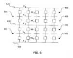
- FIG. 6is a block diagram depicting one possible configuration of four memory layers
- FIG. 7is a block diagram depicting the write circuitry on the memory circuit portion associated with half a bit block
- FIG. 8is a block diagram depicting one possible driver configuration
- FIG. 9is a block diagram depicting one possible secondary decoding circuit configuration
- FIG. 10Ais a block diagram depicting some of the systems that contribute to writing a 1 to a particular memory cell
- FIG. 10Bis a block diagram depicting some of the systems that contribute to writing a 0 to a particular memory cell
- FIG. 11Ais a block diagram depicting an example of a positive read from the array portion
- FIG. 11Bis a block diagram depicting an example of a negative read from the array portion
- FIG. 12is a block diagram of the read circuitry 1200 on the memory circuit portion 410 associated with half of a bit block;
- FIG. 13is a circuit diagram of an exemplary full bit block sensing circuit.
- the present inventionattempts to move memory technology closer to near ideal operating characteristics. It is theorized that the fundamental concepts of the present invention will ultimately allow the creation of memory that is:
- Such ideal memorywould likely need to be based on both new memory architectural features as well as new memory materials.
- Architectural featureswould probably include:
- Multi levels of memory(more than one bit/cell).
- the voltage that is used to switch the materialis consistent, and is approximately 2 to 3 volts. It should be selectable by adjusting the thickness of the material.
- the cellcan be read with a voltage, approximately 1 volt, that is lower than the write voltage and can interrogate the resistance of the memory cell without disturbing the contents of the cell, even up to 10 15 reads.
- the datais retained in the cell for up to 10 years at 125° C. after the last write to the cell.
- the cellwill operate at temperatures from ⁇ 45° C. to 85° C.
- the cellwill write up to 10 15 times without wear-out.
- the conductivity of the material in the low resistance stateis approx. 1 ⁇ -cm.
- the inventorstheorize that there are two general classes of metal oxides to research in order to determine if the material has the required electrical properties. It should be noted that the materials that have been studied to date have many if not most of the needed characteristics, though no single material has the all the optimal properties.
- Class 1The Manganites are the first class of metal oxides that should be investigated. Some examples of the particular materials are as follows: PCMO Pr .7 Ca .3 MnO 3 LCMO La .7 Ca .3 MnO 3 LSMO La .7 Sr .3 MnO 3
- Class 2The Titanates and Zirconates are the second class of materials that should be investigated. Some examples of the particular materials are as follows: SZO SrZrO 3 STO SrTiO 3
- Fabrication of thin filmsare processed by either solution based spin on followed by high temperature anneal, pulsed laser deposition (PLD), sputtering, and metalorganic chemical vapor deposition (MOCVD).
- the thin filmscan be characterized by stoichiometry, element substitution, bottom electrode (seed layer), top electrode, and deposition method.
- a high density NVRAMrequires both an array of memory cells and peripheral circuitry driving the memory cells.
- the memory cellsinclude a memory plug and a mechanism, such as conductive array lines, that deliver current to the memory plug.
- the principal components of the memory pluginclude (a) a memory element, (b) a non-ohmic device for modifying the current-voltage characteristics of the memory element, and optionally (c) other components that may be necessary in certain embodiments to address materials and fabrication considerations.
- the memory plugshould include two or more resistance states that can be distinguished during a read operation. These states should be reversible by application of a stimulus such as an electric field of specified size and polarity. Further the states should not be easily disturbed. Thus, the resistance of the material as a function of the stimulus should exhibit hysteresis.
- the memory elementsimpart the distinct resistance states.
- Memory elements with three or more distinct resistance statesallow multi-bit memory plugs (also referred to as multi-level memory plugs), which will be discussed later.
- multi-bit memory plugsalso referred to as multi-level memory plugs
- the present discussionwill focus on two-state memory plugs that store a single bit of information. Also, for consistency throughout this document, the lower resistance state of the memory plug will be referred to as providing a value of 1 and the higher resistant state will be referred to as providing a value of 0.
- the memory elementswitches between one resistance state and another by application of at least a threshold write voltage (deemed V Wth herein).
- V Wtha threshold write voltage
- To change resistance states in one directione.g., from 1 to 0
- a write voltage V Wis applied.
- a write voltage of the opposite polarity⁇ V W ) is applied.
- the magnitude of V Wmust be greater than V Wth .
- the non-ohmic deviceimparts a very high resistance at low applied voltages (and a low resistance at high voltages), which prevents the unselected plugs from being disturbed during normal read and write operations and minimizes unwanted power dissipation during such operations.
- the memory plugsare accessed via conductive lines of a cross point array, although many other configurations appropriate for particular applications.
- FIG. 1depicts the basic current-voltage characteristics of a two-state (single bit) resistive memory element suitable for use in memory plugs of this invention.
- a high resistance stateis illustrated by a V-I line 105 and a low resistance state is illustrated by a V-I line 110 . If the memory element is initially in the high resistance state 105 , and a voltage pulse of either positive or negative polarity is applied, the memory element will transition into the low resistive state 105 . Afterwards, a voltage pulse of an opposite polarity from the initialization voltage pulse will return the memory element to the high resistance state.
- the I-V characteristics depicted in FIG. 1may be acceptable for some applications, but there are two issues that encourage a modified I-V characteristic for other applications.
- unselected plugs on a selected lineare exposed to a fractional voltage, such as one-half the voltage required to read or write from the selected plug. Ideally, this fractional voltage will be in a region of the I-V profile where minimal current is drawn.
- the memory plugemploys a non-ohmic device.
- the non-ohmic devicepreferably has a high resistance when exposed to the fractional voltages and a low resistance when exposed to the full read or write voltages. Since read and write voltages are both positive and negative, the non-ohmic device is preferably, though not necessarily, symmetric and not uni-directional.
- an x direction conductive array linereceives the fractional voltage of one-half the read voltage or one-half the write voltage during read and write cycles, respectively.
- the corresponding y direction array linereceives one-half the read voltage or one-half the write voltage. That way, only the selected plug at the x-y intersection sees the full value read or write voltage, while other plugs on each line see only one-half the read or write voltage.
- a preferred memory array for use with the memory plugs of this inventionis a cross point array.
- a cross point arrayis a memory array of orthogonal conductive array lines intersecting at memory plugs.
- the memory plug footprintscorrespond closely to the perimeters defined by intersecting conductive array lines.
- memory plugs in a cross point arrayshould be small.
- the memory plugs employed in certain embodiments of this inventiondo not employ access transistors or similar active components.
- Cross point array designs suitable for use with this inventionwill be described in more detail below.
- FIG. 2AAn example of preferred I-V characteristics for a memory plug of this invention is depicted in FIG. 2A.
- the plugmay include a memory element that has the I-V characteristics depicted in FIG. 1 and a non-ohmic device that has the I-V characteristics depicted in FIG. 2B. When such components are coupled, the overall memory plug has the I-V characteristics depicted in FIG. 2A.
- the memory plughas a very high resistance regime near zero volts. This regime resides between voltages ⁇ V NO and V NO , and has a resistance designated R L . Beyond these voltages, the circuit component depicted in FIG. 2B goes to a very low resistance state labeled R NO .
- a memory plug having the characteristics depicted in FIG. 2Aresults.
- the memory plugmaintains a high resistance of R L ′ (about equal to R L ) in the voltage domain between ⁇ V NO and V NO . Beyond this domain (in both the negative and positive voltage domains), the resistance of the memory plug splits into two states R 1 and R 0 as depicted.
- FIG. 2Cdepicts the I-V characteristics shown in FIG. 2A superimposed with the indicators of read and write voltages.
- the write voltage V W and the read voltage V Rare the voltages seen by the memory element of the memory plug. If the memory plug includes additional circuitry possessing the I-V characteristics depicted in FIG. 2B, for example, then an additional read and write voltage must be defined: one that is seen by the entire memory plug, not just the memory element of that plug.
- V R ′ and V W ′The magnitudes of these whole-plug read and write voltages (denoted V R ′ and V W ′) are equal to the required read and write voltages of the memory element in combination with the additional voltage needed to compensate for the non-ohmic device (and any other additional elements that provide a voltage drop).
- a value of V R ′resides a relatively small distance on the voltage scale to the positive side of V NO , past where the two resistance states branch apart.
- ⁇ V R ′resides a relatively small distance to the negative side of ⁇ V NO on the voltage scale.
- the voltages V W ′ and ⁇ V W ′reside somewhat beyond the magnitudes of V R ′ and ⁇ V R ′ on the voltage scale.
- the plugwill also have characteristic threshold write voltages V Wth ′ and ⁇ V Wth ′, not shown, at which the resistance actually changes state. V W ′ will always greater than or equal to V Wth ′.
- V R ′a voltage of V R ′ across the memory plug.
- V W ′a voltage of V W ′ (or ⁇ V W ′) across the memory plug.
- a high-density NVRAMemploying peripheral circuitry that applies one-half of the read or write voltage via one array line and one-half of the read or write voltage (of opposite polarity) an orthogonal array line is ideally suited for use with memory plugs that have the I-V characteristics depicted in FIG. 2C.
- the memory plug I-V parameters of interestinclude R 1 and R 0 (the resistances of the memory plug when the memory element is in its low state or its high state), V W and V R (the write and read voltages experienced by the memory element), V W ′ and V R ′ (the write and read voltages experienced by the whole memory Plug), V NO (the voltage at which the memory plug transitions from a very high resistance state to two distinctly separate resistance states (R 1 and R 0 )), R L (the resistance associated with the range between ⁇ V NO and V NO for the non-ohmic device), R L ′ (the resistance associated with the range between ⁇ V NO and V NO across the entire plug), and R NO (the resistance of the non-ohmic circuit element at voltage magnitudes beyond V NO ).
- R 1 and R 0the resistances of the memory plug when the memory element is in its low state or its high state
- V W and V Rthe write and read voltages experienced by the memory element
- V W ′ and V R ′the write and read voltages experienced by
- V Wthwould be about 2V for the memory element. If a maximum current of 10 ⁇ A were desired, and the resistive states of the memory element were desired to be an order of magnitude apart, then a V R of 1V might cause a particular memory element to exhibit a low resistive state of 100 k ⁇ and a high resistive state of 1M ⁇ . A V R of 1V would also be far enough from V Wth to prevent a read from disturbing the memory element.
- a V NO of 2Vwould cause V W ′ to be 4V and V R ′ to be 3V.
- a higher V NOmight be appropriate to allow for some fabrication inconsistencies and other additional elements in the memory plug that provides a voltage drop. If the CMOS fabrication process is then restricted to having no more than ⁇ 3V on the memory device, then the maximum V W ′ would be 6V.
- V W ′would be chosen to be between 4V and 6V, V R ′ to be between 3V and 5V and V NO to be between 2V and 4V.
- the actual physical structure of a memory plugmay take many different forms. In a preferred embodiment, it minimally includes a layer of the material comprising the memory element sandwiched between two separate conductive array lines. Preferably, the memory plug will also include a non-ohmic device located with the memory element, between the two array lines. As mentioned, such non-ohmic device preferably provides the I-V characteristics depicted in FIG. 2B.
- FIG. 3Adepicts one example of a memory plug structure in a cross point array.
- a first conductive array line 305 and a second conductive array line 310serve as contacts for the memory plug.
- separate contacts or electrodesmay be provided within the memory plug. These could be conductive barrier layers, seed layers, etc. that electrically contact conductive array lines 305 and 310 .
- no such separate contactsare depicted.
- a memory element 315sits directly on lower conductive array line 310 .
- a non-ohmic circuit device 320is sandwiched between resistive memory element 315 and upper array line 305 .
- FIG. 3B and 3Cdepict a memory cell 300 , the unit that is repeated in the memory array, and more fully described in connection with FIG. 4.
- the structure depicted in FIG. 3Amay be an idealized or simplified embodiment. Typically, one or more barrier layers and/or seed layers may be required depending upon the fabrication process and the materials comprising the memory element, the non-ohmic device and the array lines.
- the non-ohmic device 320may be a multi-layered structure having a degree of complexity commensurate with the requirements of the circuit element.
- the material comprising the memory elementshould most fundamentally have I-V characteristics at least approximating those shown in FIG. 1.
- Various types of materialmeet this requirement. Many of these also exhibit colossal magnetoresistive effects. While not wishing to be bound by theory, it is believed that these various effects may derive from the same underlying physical phenomena in some materials.
- the patent application titled, “Method For Switching The Properties Of Perovskite Materials Used In Thin Film Resistors,” to Shangqing Liu, et al., U.S. Pat. No. 6,204,139fully describes various complex metal oxides exhibit the reversible multi-resistance state properties outlined above.
- U.S. Pat. No. 6,204,139is hereby incorporated by reference in its entirety for all purposes.
- Pr 0.7 Ca 0.3 MnO 3 , La 0.7 Ca 0.3 MnO 3 , Gd 0.7 Ca 0.3 BaCo 2 O 5 , SrZrO 3 , and SrTiO 3are specific examples of complex metal oxides that exhibit the desired reversible multi-resistance. In addition to being complex metal oxides, some of these materials have a perovskite crystal structure. Note that the resistive memory components employed in this invention are not limited to either complex metal oxide or perovskite crystal lattice structure. Any material approximating the V-I characteristics described above or meeting other requirements described elsewhere herein may be suitable for use as a memory element of this invention.
- the non-ohmic deviceshould have I-V characteristics at least approximating those shown in FIG. 2B.
- the elementis a combination of two oppositely oriented diodes connected in series. When two diodes are oppositely oriented, one diode's forward current is blocked by the other diode at low voltages (e.g., voltages between ⁇ V NO and V NO ). But at the breakdown voltage of each diode, the resistance to current flow diminishes greatly. Hence, in this embodiment, it is the diodes' breakdown voltages that define V NO and ⁇ V NO .
- Some well known diodesare (i) a PN junction diode, in amorphous, microcrystalline, polycrystalline or single crystal semiconductor (e.g. Si, Ge, SiGe, GaAs, InP, etc.); (ii) a metal-semiconductor Schottky diode; (iii) a junction field-effect transistor with gate connected to source (or to drain); (iv) a MOSFET with gate either floating, or connected to source or connected to drain; (v) a Zener diode, avalanche diode, or tunnel diode; (vi) a four-layer diode (SCR); (vii) a P-I-N diode in amorphous, microcrystalline, polycrystalline or single crystal semiconductor; and others that will be readily apparent to those skilled in the art.
- Another implementation of the non-ohmic devicecomprises two oppositely oriented diodes connected in parallel.
- Yet another implementationcomprises a metal-insulator-metal (MIM) tunneling device
- a preferred embodiment of the non-ohmic elementwould be constructed from the same material as the memory element. Both the non-ohmic element and the memory element could then be contained in a single layer of the memory plug.
- FIG. 4Ais a block diagram of an exemplary high-density NVRAM 400 with 32 bit blocks.
- a single bit block 402contains substantially all the circuitry that would be required to store a single bit of information.
- Each bit blockis responsible for a separate bit in a multi-bit address and provides a separate I/O operation. If the high-density NVRAM had 32 bit blocks, then 32 bits could be accessed in a single cycle.
- One benefit to designing the high density NVRAM 400 with bit blocksis that once a single bit block is designed, the same design can be replicated for each desired bit block.
- FIG. 4Bdepicts a cross-section of a bit block 402 of an exemplary high-density NVRAM 400 .
- the high-density NVRAM 400is preferably made up an array portion 405 and a memory circuit portion 410 .
- the memory circuit portion 410contains all of the active devices (devices that require a source of energy for their operation, such as transistors and amplifiers) needed to operate the high-density NVRAM 400 .
- the circuitry of the memory circuit portion 410will be described in connection with FIG. 6 and those skilled in the art will recognize that standard fabrication techniques (e.g., CMOS processing) can be used to manufacture the memory circuit portion 410 .
- the array portion 405includes a first layer of x-direction conductive array lines (X 0 layer) 415 , a second layer of x-direction conductive array lines (X 1 layer) 420 , a layer of y-direction conductive array lines (Y 0 layer) 425 , a first memory plug layer (ML 0 ) 430 situated between the X 0 layer 415 and the Y 0 layer 425 , a second memory plug layer (ML 1 ) 435 situated between the Y 0 layer 425 and the X 1 layer 420 , a first plurality of X 0 thrus 440 and a first plurality of X 1 thrus 445 .
- a plurality of vias 450 and metallization layers 455 togetherprovide conductive paths from components of the memory circuit portion 410 to memory cells of the array portion 405 .
- the thrus 440 and 445provide conductive paths from memory cells of the array portion 405 to the memory circuit portion. It should be noted that the thrus of the array portion 405 must be conductive and, therefore, will have different electrical properties that the memory layers at the same height.
- the array portion 405contains only passive devices such as the memory cell of FIG. 3B. Since no transistor or other access device is required, and each cell only needs a pair of conductive array lines and memory plug, each cell can approach a minimum cell size of 4F 2 , where F is the minimum feature size as shown in FIG. 3C. This is due to the fact that all the conductive array lines, memory plugs, and spacing in between conductive array lines can all be fabricated to a width of F. Optimally, both the top and bottom surface of the Y 0 layer 425 are used, allowing a single set of Y 0 conductive array lines to access all memory plugs in both ML 0 430 and ML 1 435 .
- the repeatable cell that makes up the array of the array portion 405can be considered to be the memory plug, plus 1 ⁇ 2 of the space around the memory plug, plus 1 ⁇ 2 of an x-direction conductive array line and 1 ⁇ 2 of a y-direction conductive array line.
- 1 ⁇ 2 of a conductive array lineis merely a theoretical construct, since a conductive array line would be the same width, regardless of whether both surfaces of the conductive array line was used. Accordingly, the top and bottom layers of conductive array lines (which use only one surface) would be fabricated to the same size as all other layers of conductive array lines.
- a single conductive array linecan safely carry half of
- FIG. 5Aillustrate an example of writing a 1
- FIG. 5Billustrates an example of writing a 0. If V W ′ is 6V and ⁇ V W ′ is ⁇ 6V, then each conductive array line must be capable of raising its voltage to 3V or lowering its voltage to ⁇ 3V.
- the array portion 405can be designed to occupy roughly the same footprint as the memory circuit portion 410 . If more storage is desired, additional memory layers can be used, adding to the height of the high-density NVRAM 400 , and not its length or width.
- FIG. 6is a block diagram of one possible configuration of four memory layers, ML 0 605 , ML 1 610 , ML 2 615 and ML 3 620 .
- ML 0 605ML 1 610
- ML 2 615ML 2 615
- ML 3 620ML 3 620
- X 0 layer 625X 1 layer 635
- Y 1 layer 640X 1 layer 635
- Y 1 layer 640X 2 645
- Table 2shows the combinations of x-direction conductive array lines and y-direction conductive array lines that are necessary to activate a memory element on a specific memory layer.
- each conductive layerwould not need to have its own separate circuitry.
- the outermost x layers of conductive array linesare logically related for accessing memory elements and may share a common set of thrus to access the same circuitry.
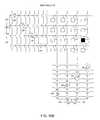
- FIG. 7is a block diagram of the write circuitry 700 on the memory circuit portion 410 associated with a portion of a given bit block. Specifically, the write circuitry 700 is appropriate only for one direction of conductive array lines. A full bit block write circuit would require write circuitry for both directions of conductive array lines.
- the write circuitry 700includes a primary decoding and data control circuit (primary decoder) 705 , a secondary decoding driver 710 , a positive voltage pump 715 , a negative voltage pump 720 , and peripheral bank circuitry 725 A, 725 B and 725 Z for driving a number of contiguous conductive array lines.
- the peripheral bank circuitry 725 A, 725 B and 725 Zis responsible for activating a sub-set of the conductive array lines that make up a single bit block.
- Each instance of peripheral bank circuitry 725 A, 725 B or 725 Zcontains a level shifter 730 , a driver 735 , secondary decoding circuitry 740 , a set of first vias 745 to the associated conductive lines, a set of second vias 750 also to the associated conductive lines, and a referencing circuit 755 that ensures the conductive array lines are grounded before or after every cycle.
- the referencing circuit 755can either be a separate from, or integrated in, the other components (e.g., driver 735 or secondary decoding circuitry 740 ), making the second set of vias 750 unnecessary.
- first set of vias 745 and the second set of vias 750there may be more than four conductive lines controlled by each via. As previously mentioned, multiple layers of conductive lines might be controlled by a single set of vias 745 and 750 .
- the inputs to the write circuitry 700include a control line 760 that carries information indicating what operation is to be performed (typically read or write), an address line 765 that carries information uniquely identifying the memory location, and a data line 770 that carries the information to be stored on the memory element.
- the primary decoder 705processes the data on the address line 765 and determines which peripheral bank circuitry 725 A, 725 B or 725 Z is associated with the memory element.
- the secondary decoding driver 710also processes the data on the address line 765 . However, instead of determining which bank is associated with the memory element, the secondary decoding driver 710 determines which “grouping” of conductive array lines is associated with the memory element. For example, the secondary decoding driver 710 might determine that the desired memory element is on the third conductive array line of a bank, but would not need to know which bank the memory element was associated with. Together, the primary decoder 705 and the secondary decoding driver 710 can identify a single conductive line associated with the selected memory element.
- the level shifter 730 , driver 735 , positive voltage pump 715 and negative voltage pump 720are all used to deliver the necessary voltage to the appropriate bank of conductive array lines during a write.
- the positive voltage pump 715steps up the V CC of the circuit to 1 ⁇ 2 V W ′ and the negative voltage pump 730 changes V CC to ⁇ 1 ⁇ 2 V W ′.
- varying the size of the voltage pumps 715 and 730would vary how many would be needed on the high-density NVRAM 400 .
- a large enough pumpcould, for example, supply both bit block halves, or even multiple bit blocks.
- a smaller pumpmight be used, for example, to drive a single instance of peripheral bank circuitry.
- the other components 705 - 770 of the write circuitry 700are required for every bit block half.
- FIG. 8is a block diagram of one possible driver 735 configuration.
- a p-channel transistor 805 and an n-channel transistor 810are arranged in series.
- the n-channel transistormay be in a separate well from the CMOS logic because its substrate is tied to a negative voltage.
- the source of the p-channel transistor 805is connected to the positive voltage pump 715 and the source of the n-channel transistor 810 is connected to the negative voltage pump 730 .
- the level shiftermust change the output voltages of the primary decoder 705 to appropriate threshold gate voltages to control driver transistors 805 and 810 .
- the primary decoder 705determines that a 1 must be written to the bank associated with the peripheral bank circuitry 725 B and the write circuitry 700 is associated with the x-direction of conductive array lines, it must send a signal that would ultimately cause the driver 735 of that bank to turn on its p-channel transistor 805 .
- the n-channel transistor 810 of that bankwould be turned off, as would all the other n-channel and p-channel transistors of all the other banks 725 A and 725 Z.
- the p-channel transistor 805 that is onwould then raise the input voltage of the secondary decoding circuitry to 1 ⁇ 2 V W ′.
- 0V from the level shifter 730would fully turn on the p-channel transistor 805 and 1 ⁇ 2 V W ′ from the level shifter 730 will fully turn off the p-channel transistor.
- the n-channel transistor 810could have similar characteristics, requiring 0V to be fully turned on and ⁇ 1 ⁇ 2 V W ′ to be fully turned off.
- FIG. 9is a block diagram of one possible secondary decoding circuit 740 configuration. If the peripheral bank circuitry 725 B were responsible for four conductive array lines, then there would be four pass devices 905 , 910 , 915 and 920 . Each pass device has an n-channel transistor and a p-channel transistor in parallel whose gates are separately controlled by the secondary decoding driver 710 and whose sources are connected to the output of the driver 730 .
- the selected pass device 915could have a threshold voltage that turns on its n-channel transistor 925 with a gate voltage of 1 ⁇ 2 V W ′ and turns on the p-channel transistor 930 with a gate voltage of 0V.
- the other three pass devices 905 , 910 and 920would be off with the gate voltages of the n-channel transistors at, for example, 0V and the gate voltage of the p-channel transistors at 1 ⁇ 2 V W ′. Since only one pass device would allow current to flow, only one via would be brought up to 1 ⁇ 2 V W ′.
- FIG. 10A and 10Bare block diagrams of some of the systems that contribute to writing a 1 or a 0 to a particular memory cell.
- the driver's 735 n-channel transistor 810would be on instead of its p-channel transistor 805 for writing a 0.
- the voltage from the driver 735would be ⁇ 1 ⁇ 2 V W ′.
- the selected pass device 915would be on when the n-channel transistor's 925 voltage is, for example, at 0V and the p-channel transistor's 930 voltage is at ⁇ 1 ⁇ 2 V W ′.
- the other three pass devices 905 , 910 and 920would be off with the gate voltage of the n-channel transistors at ⁇ 1 ⁇ 2 V W ′ and the gate voltage of the p-channel transistors at 0V.
- FIG. 11Aillustrates an example of what could be called a “positive” read
- FIG. 11Billustrates an example of what could be called a “negative” read. Both positive and negative reads deliver a full
- Switching polaritiescan be accomplished by simply having the reads alternate between positive and negative with every read. Although the chances that a single memory cell will have two consecutive reads are low, over the lifetime of the high-density NVRAM 400 all the memory cells should have had roughly the same amount of positive reads as negative reads.
- FIG. 12is a block diagram of the read circuitry 1200 on the memory circuit portion 410 associated with half of a bit block. Similar to the write circuitry 700 , the read circuitry 1200 is appropriate only for one direction of conductive array lines. A full bit block read circuit would require read circuitry for both directions of conductive array lines.
- the read circuitry 1200can use much of the same circuits as the write circuitry 700 . Fundamentally, the only two differences between the reading and writing operations are that
- a sensing circuit 1205handles the output. Optimally, the sensing circuit 1205 will compare the results from both halves of the bit block. Only a single sensing circuit 1205 is therefore required for a full bit block.
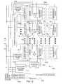
- FIG. 13is a circuit diagram of an exemplary full bit block sensing circuit 1205 .
- the sensing circuit 1300contains two inverting differential amplifiers 1305 and 1310 , two non-inverting differential amplifiers 1315 and 1320 , two AND gates 1325 and 1330 , and a multiplexer 1335 .
- the differential amplifiers 1305 , 1310 , 1315 , and 1320take their inputs from either the x-direction bit block half or the y-direction bit block half.
- the x-direction bit blockwill cause its non-inverting differential amplifier 1315 to output either a 0 signal or a 1 signal, depending on the resistive state of the memory element. If the voltage starts to increase towards the positive voltage pump 715 voltage, the non-inverting differential amplifier 1315 will output a 1 signal to the AND gate 1325 .
- the y-direction bit blockwill cause its inverting differential amplifier 1310 to output a 1 signal if the voltage starts to decrease towards the negative voltage pump 720 voltage.
- both the x-direction and the y-direction linesindicate that the selected memory cell is in its higher resistive state
- the AND gate 1325will output a 1 signal.
- the non-inverting differential amplifier 1315receives an input voltage that decreases towards 1 ⁇ 2 V R , it will output a 0 signal.
- the y-direction non-inverting differential amplifier 1315will output a 0 signal if it receives an input voltage that decreases towards ⁇ 1 ⁇ 2 V R .
- the x-direction inverting differential amplifier 1305will output a 1 signal if it receives an input voltage decreasing towards the negative voltage pump 720 voltage and the y-direction non-inverting differential amplifier 1320 will output a 1 signal if it receives an input voltage increasing towards the positive voltage pump 715 voltage, causing the appropriate AND gate 1330 to output a 1 signal.
- the multiplexer 1335selects the AND gate 1325 or 1330 that is appropriate for the polarity of the read, and outputs the result to a data output line 1210 , depicted in FIG. 12.
- the positive voltage pump 715 and the negative voltage pump 720have a static output.
- is less than
- the secondary decoding circuitneeds to pass less than the full voltage from the voltage pumps 715 and 720 . This can be accomplished by only partially turning on a transistor in the appropriate pass gate 915 . For example, if the sources of the pass device's 915 transistors are at 3V (a positive polarity read) and the p-channel transistor 930 was turned off with a gate voltage of 3V, then the n-channel transistor 925 would need to have a gate voltage of approximately 2.5V to have its drain voltage at 2V.
- the sources of the pass device's 915 transistorsare at ⁇ 3V (a negative polarity read) and the n-channel transistor 925 was turned off with a gate voltage of ⁇ 3V, then the p-channel transistor 930 would need to have a gate voltage of approximately ⁇ 2.5V to have its drain voltage at ⁇ 2V.
- An inverting circuit 1215can be used to create a feedback circuit. If the voltage from the pass device 915 starts to increase during a positive read, then the signal can be inverted, and the decreasing voltage can be used to further pull down the gate voltage of the n-channel transistor 925 . Conversely, if the voltage from the pass device 915 starts to decrease during a negative read, then the signal can be inverted, and the increasing voltage can be used to further pull up the gate voltage of the p-channel transistor 930 . Of course, the change in the gate voltage will be slight, so there is no danger of the gate voltage increasing enough to allow V Wth from being applied across the memory cell.
- a read/write pair of transistors 1220is used to block the signal from the pass devices 905 , 910 , 915 and 920 during a write operation.
- the secondary decoding circuitryworks with the primary decoding circuitry to select unique lines for access. It also distinguishes between read and write operations on a selected line. This allows the single line to both select a memory element and pass data to that element. This feature enables implementation of a cross-point architecture.
Landscapes
- Engineering & Computer Science (AREA)
- Chemical & Material Sciences (AREA)
- Materials Engineering (AREA)
- Computer Hardware Design (AREA)
- Semiconductor Memories (AREA)
Abstract
Description
- This application claims the benefit of U.S. Provisional Application No. 60/400,849, filed Aug. 02, 2002, U.S. Provisional Application No. 60/422,922, filed Oct. 31, 2002, and U.S. Provisional Application No. 60/424,083, filed Nov. 5, 2002 all of which are incorporated herein by reference in their entireties and for all purposes. This application is related to the following U.S. patent applications, all filed Dec. 23, 2002: U.S. application Ser. No. 10/330,512, entitled “Cross Point Memory Array Using Multiple Thin Films;” application Ser. No. 10/330,153, entitled “Cross Point Memory Array Using Multiple Modes of Operation;” application Ser. No. 10/330,964, entitled “Cross Point Memory Array Using Distinct Voltages;” application Ser. No. 10/330,170, entitled “Providing A Reference Voltage To A Cross Point Memory Array;” application Ser. No. 10/330,900, entitled “Cross Point Memory Array With Memory Plugs Exhibiting A Characteristic Hysteresis;” application Ser. No. 10/330,150, entitled “Multi-Output Multiplexor;” and application Ser. No. 10/330,965, entitled “Multiplexor Outputting A Reference Voltage On Unselected Lines,” all of which are hereby incorporated herein by reference in their entireties and for all purposes.[0001]
- 1. Field of The Invention[0002]
- The present invention relates generally to memory, and more specifically to NVRAM.[0003]
- 2. Description of The Related Art[0004]
- Most digital electronic systems have two generic memory requirements: an operating memory whose primary technical requirements are fast read and write and no wear out, and a storage memory (for data and/or program store) whose primary technical requirements are non-volatility and the ability to read many times without significant data degradation. The ideal memory would satisfy both these needs in a single device. In addition, the ideal memory will also achieve considerable cost/bit reductions as compared to existing memories.[0005]
- Near ideal operating characteristics might be as follows:[0006]
- Reads and writes <100 ns[0007]
- Retains data after the power supply has been removed (non-volatile)[0008]
- Operates at low power supply voltage[0009]
- Has low active and standby currents[0010]
- Does not wear out with read/write cycling[0011]
- Has low cost/bit[0012]
- Has simple read & write operation in a system[0013]
- Wear out is the phenomena whereby a memory will fail to work after a certain number of read/write cycles. This number is usually between 100,000 to 10,000,000 read/write cycles. For a memory to have zero wear out, it would need the capability of cycling a minimum of 10[0014]15read/write cycles.
- While the present semiconductor memories that are currently in high volume commercial production today are far from meeting ideal specifications, they have achieved a large measure of commercial success because they work reasonably well at an acceptable cost. The major drawbacks from currently available non-volatile memories are as follows.[0015]
- Have long write times that range from 5 us (microseconds) to 100 s of ms (milliseconds).[0016]
- Wear out after a few hundred thousand read/write cycles.[0017]
- Have a complex user operation that involves a separate erase operation.[0018]
- However, the key parameter for most markets is cost/bit. Any solution that is more costly on a cost/bit basis will likely be relegated to a niche market.[0019]
- Recently, there have been announcements of new technologies that are being investigated that could result in memories with closer to ideal operating characteristics. None of these new technologies have yet become a commercial reality. The leading contenders for the next generation memory are likely:[0020]
- MRAM-MTJ (Magnetic RAM, Magnetic Tunnel Junction)[0021]
- MRAM-GMR (Magnetic RAM, Giant Magneto Resistance)[0022]
- OUM (Ovonics Unified Memory)[0023]
- FeRAM-1T1C Ferroelectric RAM with 1 Transistor, 1 Capacitor[0024]
- FeRAM-1T Single Transistor Ferroelectric FET[0025]
- Ferroelectric Polymer[0026]
- Chalcogenide Metal (Ag) Dendrite[0027]
- There has been a fair amount of press given to each of the above technologies over the past few years. Unfortunately, none of the most promising technologies have achieved any measure of wide commercial success to date. The details on each of the above emerging memory technologies are as follows:[0028]
- MRAM-MTJ is a very complex structure, and there appears to be problems scaling the cell size and the write current. While MRAM-MTJ has performance benefits, it is significantly more expensive than other solutions. There are some technical concerns about its scalability based upon the fundamental physics of magnetic materials, which will likely be very difficult to overcome. Unless MRAM can scale to small dimensions, it will be more expensive on a cost per bit, and not achieve wide acceptance in the market.[0029]
- MRAM-GMR also is a structure that is physically large and so the same questions of cost/bit apply.[0030]
- The OUM is a memory technology that has been around for 30+ years. In the past several years there has been a renewed interest in this technology, and presently the technology is at the stage of a feasibility design. However, there are still some technical difficulties associated with this technology due to the fact that the material is heated up to its melting point, during the write operation.[0031]
- The FeRAM[0032]1T is a very new technology that solves the problem of fast writing, but has a significant cost penalty. This technology will likely never be less costly than standard Flash memory. It may have other advantages that make it suitable for certain niche applications.
- The Ferroelectric polymer memory has slow performance and high temperature operating limitations at <85° C. However, it offers significantly lower cost per bit.[0033]
- The Chalcognide Metal (Ag) Dendrite memory is in early stages of development, and its long-term success is unknown. Its electrical characteristics are such that it is unlikely to function as a non-volatile memory. Its high temperature (100° C.) characteristics are marginal as well as its data retention characteristics.[0034]
- Table 1 summarizes each of the above emerging technologies.[0035]
TABLE 1 Non-Volatile RAM Operation Cost MRAM Yes Yes High OUM Yes Yes Low FeRAM 1T1C Yes Yes Medium FeRAM 1T Yes Yes Medium Polymer Yes No Very Low Metal Dendrite ? Yes ? - The present invention provides a high density NVRAM. In one embodiment the NVRAM includes an array of memory cells capable of storing at least a megabit of information and peripheral circuitry. Each memory cell in the array includes a memory plug that includes a memory element that switches from a first resistance state to a second resistance state upon application of a first write voltage of a first polarity and reversibly switches from the second resistance state to the first resistance state upon application of a second write voltage of polarity opposite to the first polarity. The peripheral circuitry is capable of supplying the first write voltage and the second write voltage to a memory cell or a group of memory cells and is capable of determining the resistance states of a memory cell or a group of memory cells.[0036]
- In some embodiments, the NVRAM is capable of inputting and outputting N digit words and the array of memory cells and the peripheral circuitry are divided into N bit blocks such that each bit block is associated with a single digit from the N digit word and and each bit block has the essentially the same architecture.[0037]
- In other embodiments, the memory cells are arranged in a cross point array, which may have multiple layers of memory cells. In multiple-layer cross point arrays, some conductive array line layers can be commonly controlled. In yet other embodiments, the memory plugs of the cross point array may include a non-ohmic device coupled to the memory element that imparts a high resistance to the memory plug at low voltages and a low resistance to the memory plug at high voltages. Therefore, leakage current is limited at low voltages and current is able to flow at high voltages. Specifically, a low voltage might be considered to be approximately one-half of the first write voltage and approximately one-half the second write voltage. A high voltage might be the first write voltage and the second write voltage. Applying approximately one-half of the voltage to the memory plug via a first array line and applying approximately one-half of the voltage via a second array line can be used to apply a full write voltage to a particular memory cell while unselected cells are not subject to excessive current.[0038]
- In other embodiments, the second resistive state of the memory elements is at least about 10 times greater than the first resistance state.[0039]
- In other embodiments, the memory plugs of the high-density NVRAM could have three or more levels of resistive states, allowing storage of more than one bit of data per memory cell.[0040]
- In other embodiments, the high-density NVRAM also includes read circuitry that can read a stored value from a memory plug by applying approximately one-half of a first read voltage of a first polarity to the memory plug via a first array line and applying approximately one-half of the first read voltage via a second array line. It yet other embodiments, the read circuitry can additionally read a stored value from the memory plug by applying approximately one-half of a second read voltage of a polarity opposite to the first polarity to the memory plug via the first array line and applying approximately one-half of the second read voltage via the second array line.[0041]
- FIG. 1 is a graph depicting the basic current-voltage characteristics of a two-state (single bit) resistive memory element suitable for use in memory plugs;[0042]
- FIG. 2A is a graph depicting an example of preferred I-V characteristics for a memory plug;[0043]
- FIG. 2B is a graph depicting an example of preferred I-V characteristics for a non-ohmic device;[0044]
- FIG. 2C is a graph depicting an example of preferred I-V characteristics superimposed with the indicators of read and write voltages;[0045]
- FIG. 3A is a perspective view of one example of a memory plug structure in a cross point array;[0046]
- FIG. 3B is a perspective view of one example of a repeatable memory cell of the memory array;[0047]
- FIG. 3C is a plan view depicting one example of a memory cell in a memory array;[0048]
- FIG. 4A is a block diagram depicting an exemplary high-density NVRAM;[0049]
- FIG. 4B is a cross-section depicting an exemplary bit block of a high-density NVRAM;[0050]
- FIG. 5A is a block diagram depicting an example of writing a 1 to the array portion;[0051]
- FIG. 5B is a block diagram depicting an example of writing a 0 to the array portion;[0052]
- FIG. 6 is a block diagram depicting one possible configuration of four memory layers;[0053]
- FIG. 7 is a block diagram depicting the write circuitry on the memory circuit portion associated with half a bit block;[0054]
- FIG. 8 is a block diagram depicting one possible driver configuration;[0055]
- FIG. 9 is a block diagram depicting one possible secondary decoding circuit configuration;[0056]
- FIG. 10A is a block diagram depicting some of the systems that contribute to writing a 1 to a particular memory cell;[0057]
- FIG. 10B is a block diagram depicting some of the systems that contribute to writing a 0 to a particular memory cell;[0058]
- FIG. 11A is a block diagram depicting an example of a positive read from the array portion;[0059]
- FIG. 11B is a block diagram depicting an example of a negative read from the array portion;[0060]
- FIG. 12 is a block diagram of the[0061]
read circuitry 1200 on thememory circuit portion 410 associated with half of a bit block; and - FIG. 13 is a circuit diagram of an exemplary full bit block sensing circuit.[0062]
- The present invention attempts to move memory technology closer to near ideal operating characteristics. It is theorized that the fundamental concepts of the present invention will ultimately allow the creation of memory that is:[0063]
- Nonvolatile with a minimum of 10 years data retention at 125° C.[0064]
- At least ½ the cost of any other CMOS memory.[0065]
- Fast read <70 ns and Fast write <70 ns and Fast cycle time <70 ns[0066]
- Low Voltage Operation, Vcc=1.2-1.8 V[0067]
- Low Active Current <30 ma and Low Standby Current <10 ua[0068]
- No wear out after a minimum of 10[0069]15read/write cycles
- Such ideal memory would likely need to be based on both new memory architectural features as well as new memory materials. Architectural features would probably include:[0070]
- Cross point Memory Array[0071]
- Multi layers of memory[0072]
- Multi levels of memory (more than one bit/cell).[0073]
- Therefore, to make an ideal RAM not only does one need a material with the right memory characteristics, but also one that is compatible with the above chip architectural features.[0074]
- Recently discovered electrical effects in certain complex metal oxides are promising steps in the right direction. Specifically, the conductivity of the material can be switched back and forth between two values by the use of an electric field.[0075]
- However, for these newly discovered materials to be effectively used, specific electrical properties should include:[0076]
- Switches from one resistance state to another in less than 30 ns.[0077]
- The voltage that is used to switch the material is consistent, and is approximately 2 to 3 volts. It should be selectable by adjusting the thickness of the material.[0078]
- The cell can be read with a voltage, approximately 1 volt, that is lower than the write voltage and can interrogate the resistance of the memory cell without disturbing the contents of the cell, even up to 10[0079]15reads.
- The data is retained in the cell for up to 10 years at 125° C. after the last write to the cell.[0080]
- The cell will operate at temperatures from −45° C. to 85° C.[0081]
- The cell will write up to 10[0082]15times without wear-out.
- The conductivity of the material in the low resistance state is approx. 1 Ω-cm.[0083]
- The inventors theorize that there are two general classes of metal oxides to research in order to determine if the material has the required electrical properties. It should be noted that the materials that have been studied to date have many if not most of the needed characteristics, though no single material has the all the optimal properties.[0084]
- Class 1: The Manganites are the first class of metal oxides that should be investigated. Some examples of the particular materials are as follows:[0085]
PCMO Pr.7Ca.3MnO3 LCMO La.7Ca.3MnO3 LSMO La.7Sr.3MnO3 - Class 2: The Titanates and Zirconates are the second class of materials that should be investigated. Some examples of the particular materials are as follows:[0086]
SZO SrZrO3 STO SrTiO3 - Fabrication of thin films are processed by either solution based spin on followed by high temperature anneal, pulsed laser deposition (PLD), sputtering, and metalorganic chemical vapor deposition (MOCVD). The thin films can be characterized by stoichiometry, element substitution, bottom electrode (seed layer), top electrode, and deposition method.[0087]
- A high density NVRAM requires both an array of memory cells and peripheral circuitry driving the memory cells. The memory cells include a memory plug and a mechanism, such as conductive array lines, that deliver current to the memory plug.[0088]
- The principal components of the memory plug include (a) a memory element, (b) a non-ohmic device for modifying the current-voltage characteristics of the memory element, and optionally (c) other components that may be necessary in certain embodiments to address materials and fabrication considerations. Most fundamentally, the memory plug should include two or more resistance states that can be distinguished during a read operation. These states should be reversible by application of a stimulus such as an electric field of specified size and polarity. Further the states should not be easily disturbed. Thus, the resistance of the material as a function of the stimulus should exhibit hysteresis.[0089]
- The memory elements impart the distinct resistance states. Memory elements with three or more distinct resistance states allow multi-bit memory plugs (also referred to as multi-level memory plugs), which will be discussed later. The present discussion will focus on two-state memory plugs that store a single bit of information. Also, for consistency throughout this document, the lower resistance state of the memory plug will be referred to as providing a value of 1 and the higher resistant state will be referred to as providing a value of 0.[0090]
- When the stimulus driving state change is voltage, the memory element switches between one resistance state and another by application of at least a threshold write voltage (deemed V[0091]Wthherein). To change resistance states in one direction (e.g., from 1 to 0), a write voltage VWis applied. To change states in the opposite direction, a write voltage of the opposite polarity (−VW) is applied. The magnitude of VWmust be greater than VWth.
- The non-ohmic device imparts a very high resistance at low applied voltages (and a low resistance at high voltages), which prevents the unselected plugs from being disturbed during normal read and write operations and minimizes unwanted power dissipation during such operations. Preferably, the memory plugs are accessed via conductive lines of a cross point array, although many other configurations appropriate for particular applications.[0092]
- FIG. 1 depicts the basic current-voltage characteristics of a two-state (single bit) resistive memory element suitable for use in memory plugs of this invention. A high resistance state is illustrated by a[0093]
V-I line 105 and a low resistance state is illustrated by aV-I line 110. If the memory element is initially in thehigh resistance state 105, and a voltage pulse of either positive or negative polarity is applied, the memory element will transition into the lowresistive state 105. Afterwards, a voltage pulse of an opposite polarity from the initialization voltage pulse will return the memory element to the high resistance state. - The I-V characteristics depicted in FIG. 1 may be acceptable for some applications, but there are two issues that encourage a modified I-V characteristic for other applications. First, to minimize disruption of unselected plugs on a selected line during read and write operations, it may be desirable to have a very high resistance at voltages near zero. Additionally, to minimize current dissipation during normal operation, the same characteristic is desirable. In some designs, unselected plugs on a selected line are exposed to a fractional voltage, such as one-half the voltage required to read or write from the selected plug. Ideally, this fractional voltage will be in a region of the I-V profile where minimal current is drawn. To this end, the memory plug employs a non-ohmic device. The non-ohmic device preferably has a high resistance when exposed to the fractional voltages and a low resistance when exposed to the full read or write voltages. Since read and write voltages are both positive and negative, the non-ohmic device is preferably, though not necessarily, symmetric and not uni-directional.[0094]
- In the half select embodiment, an x direction conductive array line receives the fractional voltage of one-half the read voltage or one-half the write voltage during read and write cycles, respectively. Similarly, the corresponding y direction array line receives one-half the read voltage or one-half the write voltage. That way, only the selected plug at the x-y intersection sees the full value read or write voltage, while other plugs on each line see only one-half the read or write voltage. When coupled with an appropriate I-V resistance characteristic, disruption to unselected plugs and unwanted current dissipation is minimized. The half select feature will be described in more detail below.[0095]
- As indicated, a preferred memory array for use with the memory plugs of this invention is a cross point array. Generally, a cross point array is a memory array of orthogonal conductive array lines intersecting at memory plugs. The memory plug footprints correspond closely to the perimeters defined by intersecting conductive array lines. Thus, memory plugs in a cross point array should be small. To this end, the memory plugs employed in certain embodiments of this invention do not employ access transistors or similar active components. Cross point array designs suitable for use with this invention will be described in more detail below.[0096]
- An example of preferred I-V characteristics for a memory plug of this invention is depicted in FIG. 2A. Note that the plug may include a memory element that has the I-V characteristics depicted in FIG. 1 and a non-ohmic device that has the I-V characteristics depicted in FIG. 2B. When such components are coupled, the overall memory plug has the I-V characteristics depicted in FIG. 2A.[0097]
- As depicted in FIGS. 2A and 2B, the memory plug has a very high resistance regime near zero volts. This regime resides between voltages −V[0098]NOand VNO, and has a resistance designated RL. Beyond these voltages, the circuit component depicted in FIG. 2B goes to a very low resistance state labeled RNO.
- When a non-ohmic circuit element having the I-V characteristics depicted in FIG. 2B is connected in series with a memory element having the I-V characteristics depicted in FIG. 1, a memory plug having the characteristics depicted in FIG. 2A results. As shown in FIG. 2A, the memory plug maintains a high resistance of R[0099]L′ (about equal to RL) in the voltage domain between −VNOand VNO. Beyond this domain (in both the negative and positive voltage domains), the resistance of the memory plug splits into two states R1and R0as depicted.
- FIG. 2C depicts the I-V characteristics shown in FIG. 2A superimposed with the indicators of read and write voltages. To understand this FIG., recognize that there are two characteristic read voltages and two characteristic write voltages associated with the memory plug. One of these is for the simple memory element itself as depicted in FIG. 1. The other is for the overall plug, including the memory element and the non-ohmic device. As defined before, the write voltage V[0100]Wand the read voltage VRare the voltages seen by the memory element of the memory plug. If the memory plug includes additional circuitry possessing the I-V characteristics depicted in FIG. 2B, for example, then an additional read and write voltage must be defined: one that is seen by the entire memory plug, not just the memory element of that plug. The magnitudes of these whole-plug read and write voltages (denoted VR′ and VW′) are equal to the required read and write voltages of the memory element in combination with the additional voltage needed to compensate for the non-ohmic device (and any other additional elements that provide a voltage drop).
- As depicted in FIG. 2C, in a preferred implementation, a value of V[0101]R′ resides a relatively small distance on the voltage scale to the positive side of VNO, past where the two resistance states branch apart. Similarly, −VR′ resides a relatively small distance to the negative side of −VNOon the voltage scale. Further, the voltages VW′ and −VW′ reside somewhat beyond the magnitudes of VR′ and −VR′ on the voltage scale. Note that the plug will also have characteristic threshold write voltages VWth′ and −VWth′, not shown, at which the resistance actually changes state. VW′ will always greater than or equal to VWth′.
- To read from a memory plug having the I-V characteristics of FIG. 2C, one preferably applies a voltage of V[0102]R′ across the memory plug. Similarly, to write to such memory plug, one applies a voltage of VW′ (or −VW′) across the memory plug. As indicated, a high-density NVRAM employing peripheral circuitry that applies one-half of the read or write voltage via one array line and one-half of the read or write voltage (of opposite polarity) an orthogonal array line is ideally suited for use with memory plugs that have the I-V characteristics depicted in FIG. 2C.
- The memory plug I-V parameters of interest include R[0103]1and R0(the resistances of the memory plug when the memory element is in its low state or its high state), VWand VR(the write and read voltages experienced by the memory element), VW′ and VR′ (the write and read voltages experienced by the whole memory Plug), VNO(the voltage at which the memory plug transitions from a very high resistance state to two distinctly separate resistance states (R1and R0)), RL(the resistance associated with the range between −VNOand VNOfor the non-ohmic device), RL′ (the resistance associated with the range between −VNOand VNOacross the entire plug), and RNO(the resistance of the non-ohmic circuit element at voltage magnitudes beyond VNO). Some fairly straightforward design constraints allow one to implement a working memory plug.
- For example, if about 1000Å of a memory element material were used, then V[0104]Wthwould be about 2V for the memory element. If a maximum current of 10 μA were desired, and the resistive states of the memory element were desired to be an order of magnitude apart, then a VRof 1V might cause a particular memory element to exhibit a low resistive state of 100 kΩ and a high resistive state of 1MΩ. A VRof 1V would also be far enough from VWthto prevent a read from disturbing the memory element.
- For the above example, assuming there are not any other additional elements that provide a voltage drop, V[0105]NOwould need to be at least 2V to realize the full benefits of the non-ohmic circuit element during a half-select write (The minimum VNOcan be calculated from VNO=½ VW′=½ (VNO+VW)=VW). A VNOof 2V would cause VW′ to be 4V and VR′ to be 3V. However, a higher VNOmight be appropriate to allow for some fabrication inconsistencies and other additional elements in the memory plug that provides a voltage drop. If the CMOS fabrication process is then restricted to having no more than ±3V on the memory device, then the maximum VW′ would be 6V. Therefore, if 1000Å of a memory element required 2V to change its resistive state, a maximum current of 10 μA was desired, and a read operation could detect a 10× change from one resistive states to the next, VW′ would be chosen to be between 4V and 6V, VR′ to be between 3V and 5V and VNOto be between 2V and 4V.
- The actual physical structure of a memory plug may take many different forms. In a preferred embodiment, it minimally includes a layer of the material comprising the memory element sandwiched between two separate conductive array lines. Preferably, the memory plug will also include a non-ohmic device located with the memory element, between the two array lines. As mentioned, such non-ohmic device preferably provides the I-V characteristics depicted in FIG. 2B.[0106]
- FIG. 3A depicts one example of a memory plug structure in a cross point array. A first[0107]
conductive array line 305 and a secondconductive array line 310 serve as contacts for the memory plug. In other embodiments, separate contacts or electrodes may be provided within the memory plug. These could be conductive barrier layers, seed layers, etc. that electrically contactconductive array lines memory element 315 sits directly on lowerconductive array line 310. Anon-ohmic circuit device 320 is sandwiched betweenresistive memory element 315 andupper array line 305. FIG. 3B and 3C depict amemory cell 300, the unit that is repeated in the memory array, and more fully described in connection with FIG. 4. - The structure depicted in FIG. 3A may be an idealized or simplified embodiment. Typically, one or more barrier layers and/or seed layers may be required depending upon the fabrication process and the materials comprising the memory element, the non-ohmic device and the array lines. In addition, the[0108]
non-ohmic device 320 may be a multi-layered structure having a degree of complexity commensurate with the requirements of the circuit element. - The material comprising the memory element should most fundamentally have I-V characteristics at least approximating those shown in FIG. 1. Various types of material meet this requirement. Many of these also exhibit colossal magnetoresistive effects. While not wishing to be bound by theory, it is believed that these various effects may derive from the same underlying physical phenomena in some materials. The patent application titled, “Method For Switching The Properties Of Perovskite Materials Used In Thin Film Resistors,” to Shangqing Liu, et al., U.S. Pat. No. 6,204,139 fully describes various complex metal oxides exhibit the reversible multi-resistance state properties outlined above. U.S. Pat. No. 6,204,139 is hereby incorporated by reference in its entirety for all purposes.[0109]
- Pr[0110]0.7Ca0.3MnO3, La0.7Ca0.3MnO3, Gd0.7Ca0.3BaCo2O5, SrZrO3, and SrTiO3are specific examples of complex metal oxides that exhibit the desired reversible multi-resistance. In addition to being complex metal oxides, some of these materials have a perovskite crystal structure. Note that the resistive memory components employed in this invention are not limited to either complex metal oxide or perovskite crystal lattice structure. Any material approximating the V-I characteristics described above or meeting other requirements described elsewhere herein may be suitable for use as a memory element of this invention.
- As indicated, the non-ohmic device should have I-V characteristics at least approximating those shown in FIG. 2B. Various circuit components meet this requirement. In one embodiment, the element is a combination of two oppositely oriented diodes connected in series. When two diodes are oppositely oriented, one diode's forward current is blocked by the other diode at low voltages (e.g., voltages between −V[0111]NOand VNO). But at the breakdown voltage of each diode, the resistance to current flow diminishes greatly. Hence, in this embodiment, it is the diodes' breakdown voltages that define VNOand −VNO. Some well known diodes are (i) a PN junction diode, in amorphous, microcrystalline, polycrystalline or single crystal semiconductor (e.g. Si, Ge, SiGe, GaAs, InP, etc.); (ii) a metal-semiconductor Schottky diode; (iii) a junction field-effect transistor with gate connected to source (or to drain); (iv) a MOSFET with gate either floating, or connected to source or connected to drain; (v) a Zener diode, avalanche diode, or tunnel diode; (vi) a four-layer diode (SCR); (vii) a P-I-N diode in amorphous, microcrystalline, polycrystalline or single crystal semiconductor; and others that will be readily apparent to those skilled in the art. Another implementation of the non-ohmic device comprises two oppositely oriented diodes connected in parallel. Yet another implementation comprises a metal-insulator-metal (MIM) tunneling device.
- A preferred embodiment of the non-ohmic element would be constructed from the same material as the memory element. Both the non-ohmic element and the memory element could then be contained in a single layer of the memory plug.[0112]
- FIG. 4A is a block diagram of an exemplary high-[0113]
density NVRAM 400 with 32 bit blocks. A single bit block402 contains substantially all the circuitry that would be required to store a single bit of information. Each bit block is responsible for a separate bit in a multi-bit address and provides a separate I/O operation. If the high-density NVRAM had 32 bit blocks, then 32 bits could be accessed in a single cycle. One benefit to designing thehigh density NVRAM 400 with bit blocks is that once a single bit block is designed, the same design can be replicated for each desired bit block. - FIG. 4B depicts a cross-section of a bit block[0114]402 of an exemplary high-
density NVRAM 400. The high-density NVRAM 400 is preferably made up anarray portion 405 and amemory circuit portion 410. Thememory circuit portion 410 contains all of the active devices (devices that require a source of energy for their operation, such as transistors and amplifiers) needed to operate the high-density NVRAM 400. The circuitry of thememory circuit portion 410 will be described in connection with FIG. 6 and those skilled in the art will recognize that standard fabrication techniques (e.g., CMOS processing) can be used to manufacture thememory circuit portion 410. - The[0115]
array portion 405 includes a first layer of x-direction conductive array lines (X0layer)415, a second layer of x-direction conductive array lines (X1layer)420, a layer of y-direction conductive array lines (Y0layer)425, a first memory plug layer (ML0)430 situated between the X0layer415 and the Y0layer425, a second memory plug layer (ML1)435 situated between the Y0layer425 and the X1layer420, a first plurality of X0thrus440 and a first plurality of X1thrus445. A plurality ofvias 450 andmetallization layers 455 together provide conductive paths from components of thememory circuit portion 410 to memory cells of thearray portion 405. Similarly, thethrus array portion 405 to the memory circuit portion. It should be noted that the thrus of thearray portion 405 must be conductive and, therefore, will have different electrical properties that the memory layers at the same height. - Due to the limitations of the cross-section view, only a single X[0116]0conductive array line, X1conductive array line, X0thru and X1thru are visible. Additionally, although a break line is depicted, the X0conductive array lines and the X1conductive array lines should have some mechanism that completes the electrical circuit, such as a second plurality of X0thrus and a second plurality of X1thrus that connect the X0and X1conductive array lines with the
memory circuit portion 410. Similarly, although not shown in FIG. 4B, the Y0conductive array lines 425 would connect with thememory circuit portion 410 in the same manner as the X0and X1conductive array lines. - In a preferred embodiment, the[0117]
array portion 405 contains only passive devices such as the memory cell of FIG. 3B. Since no transistor or other access device is required, and each cell only needs a pair of conductive array lines and memory plug, each cell can approach a minimum cell size of 4F2, where F is the minimum feature size as shown in FIG. 3C. This is due to the fact that all the conductive array lines, memory plugs, and spacing in between conductive array lines can all be fabricated to a width of F. Optimally, both the top and bottom surface of the Y0layer425 are used, allowing a single set of Y0conductive array lines to access all memory plugs in bothML 0430 andML 1435. Therefore, the repeatable cell that makes up the array of thearray portion 405 can be considered to be the memory plug, plus ½ of the space around the memory plug, plus ½ of an x-direction conductive array line and ½ of a y-direction conductive array line. Of course, ½ of a conductive array line is merely a theoretical construct, since a conductive array line would be the same width, regardless of whether both surfaces of the conductive array line was used. Accordingly, the top and bottom layers of conductive array lines (which use only one surface) would be fabricated to the same size as all other layers of conductive array lines. - As previously discussed in connection with FIG. 2C, a single conductive array line can safely carry half of |V[0118]R′| or |VW′| without disturbing any unselected memory element. Since only a single selected memory element would receive the full |VR′| or |VW′| (½ from the x-direction and ½ from the y-direction), a single memory element can be uniquely read from or written to. FIG. 5A illustrate an example of writing a 1, and FIG. 5B illustrates an example of writing a 0. If VW′ is 6V and −VW′ is −6V, then each conductive array line must be capable of raising its voltage to 3V or lowering its voltage to −3V.
- Referring back to FIG. 4B, if size is a consideration, the[0119]
array portion 405 can be designed to occupy roughly the same footprint as thememory circuit portion 410. If more storage is desired, additional memory layers can be used, adding to the height of the high-density NVRAM 400, and not its length or width. - FIG. 6 is a block diagram of one possible configuration of four memory layers,[0120]
ML 0605,ML 1610,ML 2615 andML 3620. Assuming that at least some of the conductive array lines can be used to deliver current to the memory plugs located both above and below the associated conductive line layer, five layers of conductive array lines (X0layer625, Y0layer630, X1layer635, Y1layer640, and X2645) would be necessary. However, not every layer of conductive array lines would need to be uniquely addressable. - Table 2 shows the combinations of x-direction conductive array lines and y-direction conductive array lines that are necessary to activate a memory element on a specific memory layer.[0121]
TABLE 2 X0, X2 X1 Y0 Y1 Memory Layer x x ML0 x x ML1 x x ML2 x x ML3 - Therefore, to access a memory cell on[0122]
ML 1610, for example, one conductive array line from the X1layer630 and one conductive array line from the Y0layer635 would need to be activated. - Generally speaking, although N memory layers would require N+1 layers of conductive array lines, each conductive layer would not need to have its own separate circuitry. In this example, the outermost x layers of conductive array lines (the X[0123]0layer625 and the X2layer645) are logically related for accessing memory elements and may share a common set of thrus to access the same circuitry.
- FIG. 7 is a block diagram of the[0124]
write circuitry 700 on thememory circuit portion 410 associated with a portion of a given bit block. Specifically, thewrite circuitry 700 is appropriate only for one direction of conductive array lines. A full bit block write circuit would require write circuitry for both directions of conductive array lines. - The[0125]
write circuitry 700 includes a primary decoding and data control circuit (primary decoder)705, asecondary decoding driver 710, apositive voltage pump 715, anegative voltage pump 720, andperipheral bank circuitry peripheral bank circuitry peripheral bank circuitry level shifter 730, adriver 735,secondary decoding circuitry 740, a set offirst vias 745 to the associated conductive lines, a set ofsecond vias 750 also to the associated conductive lines, and a referencingcircuit 755 that ensures the conductive array lines are grounded before or after every cycle. The referencingcircuit 755 can either be a separate from, or integrated in, the other components (e.g.,driver 735 or secondary decoding circuitry740), making the second set ofvias 750 unnecessary. Although only four vias are shown in the first set ofvias 745 and the second set ofvias 750, there may be more than four conductive lines controlled by each via. As previously mentioned, multiple layers of conductive lines might be controlled by a single set ofvias - The inputs to the[0126]
write circuitry 700 include acontrol line 760 that carries information indicating what operation is to be performed (typically read or write), anaddress line 765 that carries information uniquely identifying the memory location, and adata line 770 that carries the information to be stored on the memory element. When a write request comes in, theprimary decoder 705 processes the data on theaddress line 765 and determines whichperipheral bank circuitry - The[0127]
secondary decoding driver 710 also processes the data on theaddress line 765. However, instead of determining which bank is associated with the memory element, thesecondary decoding driver 710 determines which “grouping” of conductive array lines is associated with the memory element. For example, thesecondary decoding driver 710 might determine that the desired memory element is on the third conductive array line of a bank, but would not need to know which bank the memory element was associated with. Together, theprimary decoder 705 and thesecondary decoding driver 710 can identify a single conductive line associated with the selected memory element. - The[0128]
level shifter 730,driver 735,positive voltage pump 715 andnegative voltage pump 720 are all used to deliver the necessary voltage to the appropriate bank of conductive array lines during a write. Thepositive voltage pump 715 steps up the VCCof the circuit to ½ VW′ and thenegative voltage pump 730 changes VCCto −½ VW′. Those skilled in the art will appreciate that varying the size of the voltage pumps715 and730 would vary how many would be needed on the high-density NVRAM 400. A large enough pump could, for example, supply both bit block halves, or even multiple bit blocks. A smaller pump might be used, for example, to drive a single instance of peripheral bank circuitry. The other components705-770 of thewrite circuitry 700, however, are required for every bit block half. - FIG. 8 is a block diagram of one[0129]
possible driver 735 configuration. A p-channel transistor 805 and an n-channel transistor 810 are arranged in series. The n-channel transistor may be in a separate well from the CMOS logic because its substrate is tied to a negative voltage. The source of the p-channel transistor 805 is connected to thepositive voltage pump 715 and the source of the n-channel transistor 810 is connected to thenegative voltage pump 730. The level shifter must change the output voltages of theprimary decoder 705 to appropriate threshold gate voltages to controldriver transistors - For example, if the[0130]
primary decoder 705 determines that a 1 must be written to the bank associated with theperipheral bank circuitry 725B and thewrite circuitry 700 is associated with the x-direction of conductive array lines, it must send a signal that would ultimately cause thedriver 735 of that bank to turn on its p-channel transistor 805. The n-channel transistor 810 of that bank would be turned off, as would all the other n-channel and p-channel transistors of all theother banks channel transistor 805 that is on would then raise the input voltage of the secondary decoding circuitry to ½ VW′. In one exemplary embodiment, 0V from thelevel shifter 730 would fully turn on the p-channel transistor 805 and ½ VW′ from thelevel shifter 730 will fully turn off the p-channel transistor. Similarly, the n-channel transistor 810 could have similar characteristics, requiring 0V to be fully turned on and −½ VW′ to be fully turned off. - FIG. 9 is a block diagram of one possible[0131]
secondary decoding circuit 740 configuration. If theperipheral bank circuitry 725B were responsible for four conductive array lines, then there would be fourpass devices secondary decoding driver 710 and whose sources are connected to the output of thedriver 730. If voltage from thedriver 735 is ½ VW′ and a write operation is desired, then the selectedpass device 915 could have a threshold voltage that turns on its n-channel transistor 925 with a gate voltage of ½ VW′ and turns on the p-channel transistor 930 with a gate voltage of 0V. Of course, only one transistor is necessary to allow current to flow, but turning on both allows the entire circuit to respond quicker. The other threepass devices - FIG. 10A and 10B are block diagrams of some of the systems that contribute to writing a 1 or a 0 to a particular memory cell. It should be noted that the driver's[0132]735 n-
channel transistor 810 would be on instead of its p-channel transistor 805 for writing a 0. As a result, the voltage from thedriver 735 would be −½ VW′. The selectedpass device 915 would be on when the n-channel transistor's925 voltage is, for example, at 0V and the p-channel transistor's 930 voltage is at −½ VW′. The other threepass devices - Those skilled in the art will appreciate that repeatedly writing a 1 or a 0 to the same memory element would not bias the memory element if already in saturation. However, if the memory element were not in saturation, then a write operation should only be performed when the value in the memory element must change. In such a case, a read operation would be necessary before determining whether a write operation was appropriate.[0133]
- The inventors theorize that, during a read operation, it would be beneficial to switch polarities of the read to minimize long-term disruption to the high-[0134]
density NVRAM 400. FIG. 11A illustrates an example of what could be called a “positive” read and FIG. 11B illustrates an example of what could be called a “negative” read. Both positive and negative reads deliver a full |VR′| across the selected memory cell. - Switching polarities can be accomplished by simply having the reads alternate between positive and negative with every read. Although the chances that a single memory cell will have two consecutive reads are low, over the lifetime of the high-[0135]
density NVRAM 400 all the memory cells should have had roughly the same amount of positive reads as negative reads. - FIG. 12 is a block diagram of the[0136]
read circuitry 1200 on thememory circuit portion 410 associated with half of a bit block. Similar to thewrite circuitry 700, theread circuitry 1200 is appropriate only for one direction of conductive array lines. A full bit block read circuit would require read circuitry for both directions of conductive array lines. - The[0137]
read circuitry 1200 can use much of the same circuits as thewrite circuitry 700. Fundamentally, the only two differences between the reading and writing operations are that |VR| is less than |VW| and an output is desired. Asensing circuit 1205 handles the output. Optimally, thesensing circuit 1205 will compare the results from both halves of the bit block. Only asingle sensing circuit 1205 is therefore required for a full bit block. - FIG. 13 is a circuit diagram of an exemplary full bit[0138]
block sensing circuit 1205. The sensing circuit1300 contains two invertingdifferential amplifiers differential amplifiers gates multiplexer 1335. - The[0139]
differential amplifiers differential amplifier 1315 to output either a 0 signal or a 1 signal, depending on the resistive state of the memory element. If the voltage starts to increase towards thepositive voltage pump 715 voltage, the non-invertingdifferential amplifier 1315 will output a 1 signal to the ANDgate 1325. Similarly, the y-direction bit block will cause its invertingdifferential amplifier 1310 to output a 1 signal if the voltage starts to decrease towards thenegative voltage pump 720 voltage. Therefore, if both the x-direction and the y-direction lines indicate that the selected memory cell is in its higher resistive state, then the ANDgate 1325 will output a 1 signal. Conversely, if the selected memory cell is in its lower resistive state, and the non-invertingdifferential amplifier 1315 receives an input voltage that decreases towards ½ VR, it will output a 0 signal. Similarly the y-direction non-invertingdifferential amplifier 1315 will output a 0 signal if it receives an input voltage that decreases towards −½ VR. - If the read polarity is shifted, then the x-direction inverting[0140]
differential amplifier 1305 will output a 1 signal if it receives an input voltage decreasing towards thenegative voltage pump 720 voltage and the y-direction non-invertingdifferential amplifier 1320 will output a 1 signal if it receives an input voltage increasing towards thepositive voltage pump 715 voltage, causing the appropriate ANDgate 1330 to output a 1 signal. Themultiplexer 1335 selects the ANDgate data output line 1210, depicted in FIG. 12. - In the embodiment depicted in FIG. 12, the[0141]
positive voltage pump 715 and thenegative voltage pump 720 have a static output. However, since |VR| is less than |VW|, the secondary decoding circuit needs to pass less than the full voltage from the voltage pumps715 and720. This can be accomplished by only partially turning on a transistor in theappropriate pass gate 915. For example, if the sources of the pass device's915 transistors are at 3V (a positive polarity read) and the p-channel transistor 930 was turned off with a gate voltage of 3V, then the n-channel transistor 925 would need to have a gate voltage of approximately 2.5V to have its drain voltage at 2V. Conversely, if the sources of the pass device's915 transistors are at −3V (a negative polarity read) and the n-channel transistor 925 was turned off with a gate voltage of −3V, then the p-channel transistor 930 would need to have a gate voltage of approximately −2.5V to have its drain voltage at −2V. - An[0142]
inverting circuit 1215 can be used to create a feedback circuit. If the voltage from thepass device 915 starts to increase during a positive read, then the signal can be inverted, and the decreasing voltage can be used to further pull down the gate voltage of the n-channel transistor 925. Conversely, if the voltage from thepass device 915 starts to decrease during a negative read, then the signal can be inverted, and the increasing voltage can be used to further pull up the gate voltage of the p-channel transistor 930. Of course, the change in the gate voltage will be slight, so there is no danger of the gate voltage increasing enough to allow VWthfrom being applied across the memory cell. - In order to prevent the feedback circuit from interfering with a write operation, a read/write pair of[0143]
transistors 1220 is used to block the signal from thepass devices - As indicated, the secondary decoding circuitry works with the primary decoding circuitry to select unique lines for access. It also distinguishes between read and write operations on a selected line. This allows the single line to both select a memory element and pass data to that element. This feature enables implementation of a cross-point architecture.[0144]
- Although the invention has been described in its presently contemplated best mode, it is clear that it is susceptible to numerous modifications, modes of operation and embodiments, all within the ability and skill of those familiar with the art and without exercise of further inventive activity. Accordingly, that which is intended to be protected by Letters Patent is set forth in the claims and includes all variations and modifications that fall within the spirit and scope of the claim.[0145]
Claims (52)
Priority Applications (2)
| Application Number | Priority Date | Filing Date | Title |
|---|---|---|---|
| US10/360,005US6917539B2 (en) | 2002-08-02 | 2003-02-07 | High-density NVRAM |
| US11/179,790US7180772B2 (en) | 2002-08-02 | 2005-07-11 | High-density NVRAM |
Applications Claiming Priority (4)
| Application Number | Priority Date | Filing Date | Title |
|---|---|---|---|
| US40084902P | 2002-08-02 | 2002-08-02 | |
| US42292202P | 2002-10-31 | 2002-10-31 | |
| US42408302P | 2002-11-05 | 2002-11-05 | |
| US10/360,005US6917539B2 (en) | 2002-08-02 | 2003-02-07 | High-density NVRAM |
Related Child Applications (1)
| Application Number | Title | Priority Date | Filing Date |
|---|---|---|---|
| US11/179,790ContinuationUS7180772B2 (en) | 2002-08-02 | 2005-07-11 | High-density NVRAM |
Publications (2)
| Publication Number | Publication Date |
|---|---|
| US20040160819A1true US20040160819A1 (en) | 2004-08-19 |
| US6917539B2 US6917539B2 (en) | 2005-07-12 |
Family
ID=32854478
Family Applications (2)
| Application Number | Title | Priority Date | Filing Date |
|---|---|---|---|
| US10/360,005Expired - LifetimeUS6917539B2 (en) | 2002-08-02 | 2003-02-07 | High-density NVRAM |
| US11/179,790Expired - LifetimeUS7180772B2 (en) | 2002-08-02 | 2005-07-11 | High-density NVRAM |
Family Applications After (1)
| Application Number | Title | Priority Date | Filing Date |
|---|---|---|---|
| US11/179,790Expired - LifetimeUS7180772B2 (en) | 2002-08-02 | 2005-07-11 | High-density NVRAM |
Country Status (1)
| Country | Link |
|---|---|
| US (2) | US6917539B2 (en) |
Cited By (32)
| Publication number | Priority date | Publication date | Assignee | Title |
|---|---|---|---|---|
| US20040180507A1 (en)* | 2003-03-10 | 2004-09-16 | Sharp Laboratories Of America, Inc. | Low temperature processing of PCMO thin film on Ir substrate for RRAM application |
| US20060087344A1 (en)* | 2004-10-27 | 2006-04-27 | Snider Gregory S | Nanoscale latches and impedance-encoded logic for use in nanoscale state machines, nanoscale pipelines, and in other nanoscale electronic circuits |
| US20060250837A1 (en)* | 2005-05-09 | 2006-11-09 | Sandisk 3D, Llc | Nonvolatile memory cell comprising a diode and a resistance-switching material |
| US20060250836A1 (en)* | 2005-05-09 | 2006-11-09 | Matrix Semiconductor, Inc. | Rewriteable memory cell comprising a diode and a resistance-switching material |
| US20060273298A1 (en)* | 2005-06-02 | 2006-12-07 | Matrix Semiconductor, Inc. | Rewriteable memory cell comprising a transistor and resistance-switching material in series |
| US20070114508A1 (en)* | 2005-11-23 | 2007-05-24 | Matrix Semiconductor, Inc. | Reversible resistivity-switching metal oxide or nitride layer with added metal |
| US20070114509A1 (en)* | 2005-11-23 | 2007-05-24 | Sandisk 3D Llc | Memory cell comprising nickel-cobalt oxide switching element |
| KR100724528B1 (en)* | 2005-04-04 | 2007-06-04 | 한국과학기술연구원 | Thin film structure for resistance change memory device and manufacturing method |
| US20070171697A1 (en)* | 2005-12-23 | 2007-07-26 | Heinz Hoenigschmid | CBRAM memory device and method for writing to a resistive memory cell in a CBRAM memory device |
| US20070228414A1 (en)* | 2006-03-31 | 2007-10-04 | Sandisk 3D, Llc | Heterojunction device comprising a semiconductor and a resistivity-switching oxide or nitride |
| US20070236981A1 (en)* | 2006-03-31 | 2007-10-11 | Sandisk 3D, Llc | Multilevel nonvolatile memory cell comprising a resistivity-switching oxide or nitride and an antifuse |
| WO2008016932A2 (en) | 2006-07-31 | 2008-02-07 | Sandisk 3D Llc | Method and apparatus for passive element memory array incorporating reversible polarity word line and bit line decoders |
| US20080310209A1 (en)* | 2007-06-14 | 2008-12-18 | Micron Technology, Inc. | Circuit, biasing scheme and fabrication method for diode accesed cross-point resistive memory array |
| US20090001342A1 (en)* | 2007-06-29 | 2009-01-01 | April Schricker | Memory cell that employs a selectively grown reversible resistance-switching element and methods of forming the same |
| US20090001344A1 (en)* | 2007-06-29 | 2009-01-01 | April Schricker | Memory cell that employs a selectively grown reversible resistance-switching element and methods of forming the same |
| US20090001345A1 (en)* | 2007-06-29 | 2009-01-01 | April Schricker | Memory cell that employs a selectively deposited reversible resistance-switching element and methods of forming the same |
| US20090001343A1 (en)* | 2007-06-29 | 2009-01-01 | April Schricker | Memory cell that employs a selectively deposited reversible resistance-switching element and methods of forming the same |
| US20090052225A1 (en)* | 2005-01-24 | 2009-02-26 | Hidenori Morimoto | Nonvolatile Semiconductor Memory Device |
| US20090097295A1 (en)* | 2005-12-16 | 2009-04-16 | Hidenori Morimoto | Nonvolatile Semiconductor Memory Device |
| US7521705B2 (en) | 2005-08-15 | 2009-04-21 | Micron Technology, Inc. | Reproducible resistance variable insulating memory devices having a shaped bottom electrode |
| WO2010005864A1 (en)* | 2008-07-09 | 2010-01-14 | Sandisk 3D Llc | Memory cell with multiple series passive element for three-dimensional arrays |
| US20100008124A1 (en)* | 2008-07-09 | 2010-01-14 | Sandisk 3D Llc | Cross point memory cell with distributed diodes and method of making same |
| US20100157653A1 (en)* | 2008-12-19 | 2010-06-24 | Sandisk 3D Llc | Quad memory cell and method of making same |
| US20100155689A1 (en)* | 2008-12-19 | 2010-06-24 | Sandisk 3D Llc | Quad memory cell and method of making same |
| US7829875B2 (en) | 2006-03-31 | 2010-11-09 | Sandisk 3D Llc | Nonvolatile rewritable memory cell comprising a resistivity-switching oxide or nitride and an antifuse |
| US7932548B2 (en) | 2006-07-14 | 2011-04-26 | 4D-S Pty Ltd. | Systems and methods for fabricating self-aligned memory cell |
| US8308915B2 (en) | 2006-09-14 | 2012-11-13 | 4D-S Pty Ltd. | Systems and methods for magnetron deposition |
| US8395199B2 (en) | 2006-03-25 | 2013-03-12 | 4D-S Pty Ltd. | Systems and methods for fabricating self-aligned memory cell |
| US8454810B2 (en) | 2006-07-14 | 2013-06-04 | 4D-S Pty Ltd. | Dual hexagonal shaped plasma source |
| USRE46022E1 (en)* | 2005-02-02 | 2016-05-31 | Xenogenic Development Limited Liability Company | Nonvolatile semiconductor storage device and method for operating same |
| US20210184113A1 (en)* | 2019-12-17 | 2021-06-17 | International Business Machines Corporation | Conductive Oxide Diffusion Barrier for Laser Crystallization |
| EP3926632A3 (en)* | 2008-01-15 | 2022-03-09 | Micron Technology, Inc. | Memory cells, memory cell programming methods, memory cell reading methods, memory cell operating methods, and memory devices |
Families Citing this family (59)
| Publication number | Priority date | Publication date | Assignee | Title |
|---|---|---|---|---|
| US6751149B2 (en)* | 2002-03-22 | 2004-06-15 | Micron Technology, Inc. | Magnetic tunneling junction antifuse device |
| US6831854B2 (en)* | 2002-08-02 | 2004-12-14 | Unity Semiconductor Corporation | Cross point memory array using distinct voltages |
| US6906939B2 (en)* | 2002-08-02 | 2005-06-14 | Unity Semiconductor Corporation | Re-writable memory with multiple memory layers |
| US7009235B2 (en)* | 2003-11-10 | 2006-03-07 | Unity Semiconductor Corporation | Conductive memory stack with non-uniform width |
| US6917539B2 (en)* | 2002-08-02 | 2005-07-12 | Unity Semiconductor Corporation | High-density NVRAM |
| US6882553B2 (en)* | 2002-08-08 | 2005-04-19 | Micron Technology Inc. | Stacked columnar resistive memory structure and its method of formation and operation |
| US6962648B2 (en)* | 2003-09-15 | 2005-11-08 | Global Silicon Net Corp. | Back-biased face target sputtering |
| US20050138012A1 (en)* | 2003-12-23 | 2005-06-23 | Royer Robert J.Jr. | Meta-data storage and access techniques |
| US20060171200A1 (en) | 2004-02-06 | 2006-08-03 | Unity Semiconductor Corporation | Memory using mixed valence conductive oxides |
| US7082052B2 (en) | 2004-02-06 | 2006-07-25 | Unity Semiconductor Corporation | Multi-resistive state element with reactive metal |
| CN100422962C (en)* | 2004-02-27 | 2008-10-01 | 松下电器产业株式会社 | semiconductor storage device |
| US20060049435A1 (en)* | 2004-09-07 | 2006-03-09 | Spansion, Llc | Vertical JFET as used for selective component in a memory array |
| US7425504B2 (en)* | 2004-10-15 | 2008-09-16 | 4D-S Pty Ltd. | Systems and methods for plasma etching |
| US20060081467A1 (en)* | 2004-10-15 | 2006-04-20 | Makoto Nagashima | Systems and methods for magnetron deposition |
| US20060081466A1 (en)* | 2004-10-15 | 2006-04-20 | Makoto Nagashima | High uniformity 1-D multiple magnet magnetron source |
| KR100682895B1 (en)* | 2004-11-06 | 2007-02-15 | 삼성전자주식회사 | Nonvolatile Memory Device Using Resistor with Various Resistance States and Its Operation Method |
| US20130082232A1 (en) | 2011-09-30 | 2013-04-04 | Unity Semiconductor Corporation | Multi Layered Conductive Metal Oxide Structures And Methods For Facilitating Enhanced Performance Characteristics Of Two Terminal Memory Cells |
| US8937292B2 (en) | 2011-08-15 | 2015-01-20 | Unity Semiconductor Corporation | Vertical cross point arrays for ultra high density memory applications |
| US7897951B2 (en)* | 2007-07-26 | 2011-03-01 | Unity Semiconductor Corporation | Continuous plane of thin-film materials for a two-terminal cross-point memory |
| US8565003B2 (en) | 2011-06-28 | 2013-10-22 | Unity Semiconductor Corporation | Multilayer cross-point memory array having reduced disturb susceptibility |
| US8270193B2 (en) | 2010-01-29 | 2012-09-18 | Unity Semiconductor Corporation | Local bit lines and methods of selecting the same to access memory elements in cross-point arrays |
| US8559209B2 (en) | 2011-06-10 | 2013-10-15 | Unity Semiconductor Corporation | Array voltage regulating technique to enable data operations on large cross-point memory arrays with resistive memory elements |
| US7362604B2 (en)* | 2005-07-11 | 2008-04-22 | Sandisk 3D Llc | Apparatus and method for programming an array of nonvolatile memory cells including switchable resistor memory elements |
| US7345907B2 (en)* | 2005-07-11 | 2008-03-18 | Sandisk 3D Llc | Apparatus and method for reading an array of nonvolatile memory cells including switchable resistor memory elements |
| US7327603B2 (en)* | 2005-08-16 | 2008-02-05 | Infineon Technologies Ag | Memory device including electrical circuit configured to provide reversible bias across the PMC memory cell to perform erase and write functions |
| US20070084717A1 (en)* | 2005-10-16 | 2007-04-19 | Makoto Nagashima | Back-biased face target sputtering based high density non-volatile caching data storage |
| US20070084716A1 (en)* | 2005-10-16 | 2007-04-19 | Makoto Nagashima | Back-biased face target sputtering based high density non-volatile data storage |
| US20080011603A1 (en)* | 2006-07-14 | 2008-01-17 | Makoto Nagashima | Ultra high vacuum deposition of PCMO material |
| US8279704B2 (en)* | 2006-07-31 | 2012-10-02 | Sandisk 3D Llc | Decoder circuitry providing forward and reverse modes of memory array operation and method for biasing same |
| US7542338B2 (en)* | 2006-07-31 | 2009-06-02 | Sandisk 3D Llc | Method for reading a multi-level passive element memory cell array |
| US7542337B2 (en)* | 2006-07-31 | 2009-06-02 | Sandisk 3D Llc | Apparatus for reading a multi-level passive element memory cell array |
| US9236381B2 (en)* | 2006-11-17 | 2016-01-12 | Panasonic Intellectual Property Management Co., Ltd. | Nonvolatile memory element, nonvolatile memory apparatus, nonvolatile semiconductor apparatus, and method of manufacturing nonvolatile memory element |
| KR100855965B1 (en)* | 2007-01-04 | 2008-09-02 | 삼성전자주식회사 | Bidirectional JRAM having a subcell array and data writing method using the same |
| EP2128901A4 (en)* | 2007-03-22 | 2013-01-09 | Panasonic Corp | STORAGE ELEMENT AND STORAGE DEVICE |
| US8737151B2 (en) | 2007-07-26 | 2014-05-27 | Unity Semiconductor Corporation | Low read current architecture for memory |
| US8301912B2 (en) | 2007-12-31 | 2012-10-30 | Sandisk Technologies Inc. | System, method and memory device providing data scrambling compatible with on-chip copy operation |
| JP4709868B2 (en) | 2008-03-17 | 2011-06-29 | 株式会社東芝 | Semiconductor memory device |
| EP2107571B1 (en)* | 2008-04-03 | 2012-04-25 | Semiconductor Energy Laboratory Co, Ltd. | Semiconductor device |
| US7974119B2 (en) | 2008-07-10 | 2011-07-05 | Seagate Technology Llc | Transmission gate-based spin-transfer torque memory unit |
| WO2010004675A1 (en)* | 2008-07-11 | 2010-01-14 | パナソニック株式会社 | Current reduction element, memory element, and methods for manufacture of the elements |
| JP5085446B2 (en)* | 2008-07-14 | 2012-11-28 | 株式会社東芝 | 3D memory device |
| US7936580B2 (en) | 2008-10-20 | 2011-05-03 | Seagate Technology Llc | MRAM diode array and access method |
| US9030867B2 (en)* | 2008-10-20 | 2015-05-12 | Seagate Technology Llc | Bipolar CMOS select device for resistive sense memory |
| US7936583B2 (en) | 2008-10-30 | 2011-05-03 | Seagate Technology Llc | Variable resistive memory punchthrough access method |
| US7944730B2 (en)* | 2008-10-31 | 2011-05-17 | Seagate Technology Llc | Write method with voltage line tuning |
| US7825478B2 (en)* | 2008-11-07 | 2010-11-02 | Seagate Technology Llc | Polarity dependent switch for resistive sense memory |
| US8178864B2 (en) | 2008-11-18 | 2012-05-15 | Seagate Technology Llc | Asymmetric barrier diode |
| US8203869B2 (en) | 2008-12-02 | 2012-06-19 | Seagate Technology Llc | Bit line charge accumulation sensing for resistive changing memory |
| US8159856B2 (en) | 2009-07-07 | 2012-04-17 | Seagate Technology Llc | Bipolar select device for resistive sense memory |
| US8158964B2 (en) | 2009-07-13 | 2012-04-17 | Seagate Technology Llc | Schottky diode switch and memory units containing the same |
| US7936585B2 (en)* | 2009-07-13 | 2011-05-03 | Seagate Technology Llc | Non-volatile memory cell with non-ohmic selection layer |
| US8233309B2 (en)* | 2009-10-26 | 2012-07-31 | Sandisk 3D Llc | Non-volatile memory array architecture incorporating 1T-1R near 4F2 memory cell |
| US8638584B2 (en)* | 2010-02-02 | 2014-01-28 | Unity Semiconductor Corporation | Memory architectures and techniques to enhance throughput for cross-point arrays |
| KR101528209B1 (en)* | 2010-11-19 | 2015-06-11 | 휴렛-팩커드 디벨롭먼트 컴퍼니, 엘.피. | Method and circuit for switching a memristive device in an array |
| US8648426B2 (en) | 2010-12-17 | 2014-02-11 | Seagate Technology Llc | Tunneling transistors |
| US10566056B2 (en) | 2011-06-10 | 2020-02-18 | Unity Semiconductor Corporation | Global bit line pre-charge circuit that compensates for process, operating voltage, and temperature variations |
| US8891276B2 (en) | 2011-06-10 | 2014-11-18 | Unity Semiconductor Corporation | Memory array with local bitlines and local-to-global bitline pass gates and gain stages |
| US9117495B2 (en) | 2011-06-10 | 2015-08-25 | Unity Semiconductor Corporation | Global bit line pre-charge circuit that compensates for process, operating voltage, and temperature variations |
| US9484089B2 (en) | 2014-10-20 | 2016-11-01 | Sandisk Technologies Llc | Dual polarity read operation |
Citations (26)
| Publication number | Priority date | Publication date | Assignee | Title |
|---|---|---|---|---|
| US5496759A (en)* | 1994-12-29 | 1996-03-05 | Honeywell Inc. | Highly producible magnetoresistive RAM process |
| US5640343A (en)* | 1996-03-18 | 1997-06-17 | International Business Machines Corporation | Magnetic memory array using magnetic tunnel junction devices in the memory cells |
| US5792569A (en)* | 1996-03-19 | 1998-08-11 | International Business Machines Corporation | Magnetic devices and sensors based on perovskite manganese oxide materials |
| US5838608A (en)* | 1997-06-16 | 1998-11-17 | Motorola, Inc. | Multi-layer magnetic random access memory and method for fabricating thereof |
| US5920500A (en)* | 1996-08-23 | 1999-07-06 | Motorola, Inc. | Magnetic random access memory having stacked memory cells and fabrication method therefor |
| US5946227A (en)* | 1998-07-20 | 1999-08-31 | Motorola, Inc. | Magnetoresistive random access memory with shared word and digit lines |
| US6055178A (en)* | 1998-12-18 | 2000-04-25 | Motorola, Inc. | Magnetic random access memory with a reference memory array |
| US6111781A (en)* | 1998-08-03 | 2000-08-29 | Motorola, Inc. | Magnetic random access memory array divided into a plurality of memory banks |
| US6128214A (en)* | 1999-03-29 | 2000-10-03 | Hewlett-Packard | Molecular wire crossbar memory |
| US6178131B1 (en)* | 1999-01-11 | 2001-01-23 | Ball Semiconductor, Inc. | Magnetic random access memory |
| US6204139B1 (en)* | 1998-08-25 | 2001-03-20 | University Of Houston | Method for switching the properties of perovskite materials used in thin film resistors |
| US6226160B1 (en)* | 1999-04-15 | 2001-05-01 | International Business Machines Corporation | Small area magnetic tunnel junction devices with low resistance and high magnetoresistance |
| US6236590B1 (en)* | 2000-07-21 | 2001-05-22 | Hewlett-Packard Company | Optimal write conductors layout for improved performance in MRAM |
| US6242770B1 (en)* | 1998-08-31 | 2001-06-05 | Gary Bela Bronner | Diode connected to a magnetic tunnel junction and self aligned with a metallic conductor and method for forming the same |
| US6256223B1 (en)* | 1998-07-28 | 2001-07-03 | International Business Machines Corporation | Current-induced magnetic switching device and memory including the same |
| US20010023992A1 (en)* | 2000-03-27 | 2001-09-27 | Andreas Doll | Highly integrated system-on-chip system with non-volatile memory unit |
| US20010048608A1 (en)* | 2000-05-15 | 2001-12-06 | Nec Corporation | Magnetic random access memory circuit |
| US6331944B1 (en)* | 2000-04-13 | 2001-12-18 | International Business Machines Corporation | Magnetic random access memory using a series tunnel element select mechanism |
| US20020000597A1 (en)* | 2000-06-30 | 2002-01-03 | Takeshi Okazawa | Nonvolatile semiconductor memory device and method for recording information |
| US20020001224A1 (en)* | 2000-07-03 | 2002-01-03 | Peter Poechmueller | Integrated memory having memory cells with a magnetoresistive storage property and method of operating such a memory |
| US6473332B1 (en)* | 2001-04-04 | 2002-10-29 | The University Of Houston System | Electrically variable multi-state resistance computing |
| US20030003675A1 (en)* | 2001-06-28 | 2003-01-02 | Hsu Sheng Teng | Shared bit line cross point memory array |
| US20030001178A1 (en)* | 2001-06-28 | 2003-01-02 | Hsu Sheng Teng | Low cross-talk electrically programmable resistance cross point memory |
| US6531371B2 (en)* | 2001-06-28 | 2003-03-11 | Sharp Laboratories Of America, Inc. | Electrically programmable resistance cross point memory |
| US6534326B1 (en)* | 2002-03-13 | 2003-03-18 | Sharp Laboratories Of America, Inc. | Method of minimizing leakage current and improving breakdown voltage of polycrystalline memory thin films |
| US20040160818A1 (en)* | 2002-08-02 | 2004-08-19 | Unity Semiconductor Corporation | Cross point memory array using multiple modes of operation |
Family Cites Families (8)
| Publication number | Priority date | Publication date | Assignee | Title |
|---|---|---|---|---|
| US3886577A (en)* | 1973-09-12 | 1975-05-27 | Energy Conversion Devices Inc | Filament-type memory semiconductor device and method of making the same |
| US5296716A (en)* | 1991-01-18 | 1994-03-22 | Energy Conversion Devices, Inc. | Electrically erasable, directly overwritable, multibit single cell memory elements and arrays fabricated therefrom |
| US6856536B2 (en)* | 2002-08-02 | 2005-02-15 | Unity Semiconductor Corporation | Non-volatile memory with a single transistor and resistive memory element |
| US6906939B2 (en)* | 2002-08-02 | 2005-06-14 | Unity Semiconductor Corporation | Re-writable memory with multiple memory layers |
| US6836421B2 (en)* | 2002-08-02 | 2004-12-28 | Unity Semiconductor Corporation | Line drivers that fit within a specified line pitch |
| US6917539B2 (en)* | 2002-08-02 | 2005-07-12 | Unity Semiconductor Corporation | High-density NVRAM |
| US6753561B1 (en)* | 2002-08-02 | 2004-06-22 | Unity Semiconductor Corporation | Cross point memory array using multiple thin films |
| US7608467B2 (en)* | 2004-01-13 | 2009-10-27 | Board of Regents University of Houston | Switchable resistive perovskite microelectronic device with multi-layer thin film structure |
- 2003
- 2003-02-07USUS10/360,005patent/US6917539B2/ennot_activeExpired - Lifetime
- 2005
- 2005-07-11USUS11/179,790patent/US7180772B2/ennot_activeExpired - Lifetime
Patent Citations (27)
| Publication number | Priority date | Publication date | Assignee | Title |
|---|---|---|---|---|
| US5496759A (en)* | 1994-12-29 | 1996-03-05 | Honeywell Inc. | Highly producible magnetoresistive RAM process |
| US5640343A (en)* | 1996-03-18 | 1997-06-17 | International Business Machines Corporation | Magnetic memory array using magnetic tunnel junction devices in the memory cells |
| US5793697A (en)* | 1996-03-18 | 1998-08-11 | International Business Machines Corporation | Read circuit for magnetic memory array using magnetic tunnel junction devices |
| US5792569A (en)* | 1996-03-19 | 1998-08-11 | International Business Machines Corporation | Magnetic devices and sensors based on perovskite manganese oxide materials |
| US5920500A (en)* | 1996-08-23 | 1999-07-06 | Motorola, Inc. | Magnetic random access memory having stacked memory cells and fabrication method therefor |
| US5838608A (en)* | 1997-06-16 | 1998-11-17 | Motorola, Inc. | Multi-layer magnetic random access memory and method for fabricating thereof |
| US5946227A (en)* | 1998-07-20 | 1999-08-31 | Motorola, Inc. | Magnetoresistive random access memory with shared word and digit lines |
| US6256223B1 (en)* | 1998-07-28 | 2001-07-03 | International Business Machines Corporation | Current-induced magnetic switching device and memory including the same |
| US6111781A (en)* | 1998-08-03 | 2000-08-29 | Motorola, Inc. | Magnetic random access memory array divided into a plurality of memory banks |
| US6204139B1 (en)* | 1998-08-25 | 2001-03-20 | University Of Houston | Method for switching the properties of perovskite materials used in thin film resistors |
| US6242770B1 (en)* | 1998-08-31 | 2001-06-05 | Gary Bela Bronner | Diode connected to a magnetic tunnel junction and self aligned with a metallic conductor and method for forming the same |
| US6055178A (en)* | 1998-12-18 | 2000-04-25 | Motorola, Inc. | Magnetic random access memory with a reference memory array |
| US6178131B1 (en)* | 1999-01-11 | 2001-01-23 | Ball Semiconductor, Inc. | Magnetic random access memory |
| US6128214A (en)* | 1999-03-29 | 2000-10-03 | Hewlett-Packard | Molecular wire crossbar memory |
| US6226160B1 (en)* | 1999-04-15 | 2001-05-01 | International Business Machines Corporation | Small area magnetic tunnel junction devices with low resistance and high magnetoresistance |
| US20010023992A1 (en)* | 2000-03-27 | 2001-09-27 | Andreas Doll | Highly integrated system-on-chip system with non-volatile memory unit |
| US6331944B1 (en)* | 2000-04-13 | 2001-12-18 | International Business Machines Corporation | Magnetic random access memory using a series tunnel element select mechanism |
| US20010048608A1 (en)* | 2000-05-15 | 2001-12-06 | Nec Corporation | Magnetic random access memory circuit |
| US20020000597A1 (en)* | 2000-06-30 | 2002-01-03 | Takeshi Okazawa | Nonvolatile semiconductor memory device and method for recording information |
| US20020001224A1 (en)* | 2000-07-03 | 2002-01-03 | Peter Poechmueller | Integrated memory having memory cells with a magnetoresistive storage property and method of operating such a memory |
| US6236590B1 (en)* | 2000-07-21 | 2001-05-22 | Hewlett-Packard Company | Optimal write conductors layout for improved performance in MRAM |
| US6473332B1 (en)* | 2001-04-04 | 2002-10-29 | The University Of Houston System | Electrically variable multi-state resistance computing |
| US20030003675A1 (en)* | 2001-06-28 | 2003-01-02 | Hsu Sheng Teng | Shared bit line cross point memory array |
| US20030001178A1 (en)* | 2001-06-28 | 2003-01-02 | Hsu Sheng Teng | Low cross-talk electrically programmable resistance cross point memory |
| US6531371B2 (en)* | 2001-06-28 | 2003-03-11 | Sharp Laboratories Of America, Inc. | Electrically programmable resistance cross point memory |
| US6534326B1 (en)* | 2002-03-13 | 2003-03-18 | Sharp Laboratories Of America, Inc. | Method of minimizing leakage current and improving breakdown voltage of polycrystalline memory thin films |
| US20040160818A1 (en)* | 2002-08-02 | 2004-08-19 | Unity Semiconductor Corporation | Cross point memory array using multiple modes of operation |
Cited By (76)
| Publication number | Priority date | Publication date | Assignee | Title |
|---|---|---|---|---|
| US6911361B2 (en)* | 2003-03-10 | 2005-06-28 | Sharp Laboratories Of America, Inc. | Low temperature processing of PCMO thin film on Ir substrate for RRAM application |
| US20040180507A1 (en)* | 2003-03-10 | 2004-09-16 | Sharp Laboratories Of America, Inc. | Low temperature processing of PCMO thin film on Ir substrate for RRAM application |
| US20060087344A1 (en)* | 2004-10-27 | 2006-04-27 | Snider Gregory S | Nanoscale latches and impedance-encoded logic for use in nanoscale state machines, nanoscale pipelines, and in other nanoscale electronic circuits |
| WO2006049881A1 (en)* | 2004-10-27 | 2006-05-11 | Hewlett-Packard Development Company, L.P. | Nanoscale latches and impedance-encoded logic for use in nanoscale state machines, nanoscale pipelines, and in other nanoscale electronic circuits |
| CN101048824B (en)* | 2004-10-27 | 2011-09-21 | 惠普开发有限公司 | Nanoscale latches and impedance-encoded logic circuits for nanoscale electronic circuits |
| US7242215B2 (en) | 2004-10-27 | 2007-07-10 | Hewlett-Packard Development Company, L.P. | Nanoscale latches and impedance-encoded logic for use in nanoscale state machines, nanoscale pipelines, and in other nanoscale electronic circuits |
| US20090052225A1 (en)* | 2005-01-24 | 2009-02-26 | Hidenori Morimoto | Nonvolatile Semiconductor Memory Device |
| USRE46022E1 (en)* | 2005-02-02 | 2016-05-31 | Xenogenic Development Limited Liability Company | Nonvolatile semiconductor storage device and method for operating same |
| KR100724528B1 (en)* | 2005-04-04 | 2007-06-04 | 한국과학기술연구원 | Thin film structure for resistance change memory device and manufacturing method |
| US8687410B2 (en) | 2005-05-09 | 2014-04-01 | Sandisk 3D Llc | Nonvolatile memory cell comprising a diode and a resistance-switching material |
| US20060250837A1 (en)* | 2005-05-09 | 2006-11-09 | Sandisk 3D, Llc | Nonvolatile memory cell comprising a diode and a resistance-switching material |
| US20060250836A1 (en)* | 2005-05-09 | 2006-11-09 | Matrix Semiconductor, Inc. | Rewriteable memory cell comprising a diode and a resistance-switching material |
| US7812404B2 (en) | 2005-05-09 | 2010-10-12 | Sandisk 3D Llc | Nonvolatile memory cell comprising a diode and a resistance-switching material |
| US20060273298A1 (en)* | 2005-06-02 | 2006-12-07 | Matrix Semiconductor, Inc. | Rewriteable memory cell comprising a transistor and resistance-switching material in series |
| US20110070714A1 (en)* | 2005-08-15 | 2011-03-24 | Jun Liu | Reproducible resistnance variable insulating memory devices and methods for forming same |
| US8039300B2 (en) | 2005-08-15 | 2011-10-18 | Micron Technology, Inc. | Reproducible resistance variable insulating memory devices and methods for forming same |
| US8476613B2 (en) | 2005-08-15 | 2013-07-02 | Micron Technology, Inc. | Reproducible resistance variable insulating memory devices and methods for forming same |
| US7863595B2 (en) | 2005-08-15 | 2011-01-04 | Micron Technology, Inc. | Reproducible resistance variable insulating memory devices having a shaped bottom electrode |
| US7521705B2 (en) | 2005-08-15 | 2009-04-21 | Micron Technology, Inc. | Reproducible resistance variable insulating memory devices having a shaped bottom electrode |
| US20090179188A1 (en)* | 2005-08-15 | 2009-07-16 | Jun Liu | Reproducible resistance variable insulating memory devices having a shaped bottom electrode |
| US7816659B2 (en) | 2005-11-23 | 2010-10-19 | Sandisk 3D Llc | Devices having reversible resistivity-switching metal oxide or nitride layer with added metal |
| US7834338B2 (en) | 2005-11-23 | 2010-11-16 | Sandisk 3D Llc | Memory cell comprising nickel-cobalt oxide switching element |
| US20070114508A1 (en)* | 2005-11-23 | 2007-05-24 | Matrix Semiconductor, Inc. | Reversible resistivity-switching metal oxide or nitride layer with added metal |
| US20070114509A1 (en)* | 2005-11-23 | 2007-05-24 | Sandisk 3D Llc | Memory cell comprising nickel-cobalt oxide switching element |
| US7688614B2 (en) | 2005-12-16 | 2010-03-30 | Sharp Kabushiki Kaisha | Nonvolatile semiconductor memory device |
| US20090097295A1 (en)* | 2005-12-16 | 2009-04-16 | Hidenori Morimoto | Nonvolatile Semiconductor Memory Device |
| US7518902B2 (en)* | 2005-12-23 | 2009-04-14 | Infineon Technologies Ag | Resistive memory device and method for writing to a resistive memory cell in a resistive memory device |
| US20070171697A1 (en)* | 2005-12-23 | 2007-07-26 | Heinz Hoenigschmid | CBRAM memory device and method for writing to a resistive memory cell in a CBRAM memory device |
| US8395199B2 (en) | 2006-03-25 | 2013-03-12 | 4D-S Pty Ltd. | Systems and methods for fabricating self-aligned memory cell |
| US7808810B2 (en) | 2006-03-31 | 2010-10-05 | Sandisk 3D Llc | Multilevel nonvolatile memory cell comprising a resistivity-switching oxide or nitride and an antifuse |
| US8592792B2 (en) | 2006-03-31 | 2013-11-26 | Sandisk 3D Llc | Heterojunction device comprising a semiconductor oxide and a resistivity-switching oxide or nitride |
| US8227787B2 (en) | 2006-03-31 | 2012-07-24 | Sandisk 3D Llc | Heterojunction device comprising a semiconductor and a resistivity-switching oxide or nitride |
| US20110114913A1 (en)* | 2006-03-31 | 2011-05-19 | Tanmay Kumar | Heterojunction device comprising a semiconductor and a resistivity-switching oxide or nitride |
| US7875871B2 (en) | 2006-03-31 | 2011-01-25 | Sandisk 3D Llc | Heterojunction device comprising a semiconductor and a resistivity-switching oxide or nitride |
| US7829875B2 (en) | 2006-03-31 | 2010-11-09 | Sandisk 3D Llc | Nonvolatile rewritable memory cell comprising a resistivity-switching oxide or nitride and an antifuse |
| US20070236981A1 (en)* | 2006-03-31 | 2007-10-11 | Sandisk 3D, Llc | Multilevel nonvolatile memory cell comprising a resistivity-switching oxide or nitride and an antifuse |
| US20070228414A1 (en)* | 2006-03-31 | 2007-10-04 | Sandisk 3D, Llc | Heterojunction device comprising a semiconductor and a resistivity-switching oxide or nitride |
| US7932548B2 (en) | 2006-07-14 | 2011-04-26 | 4D-S Pty Ltd. | Systems and methods for fabricating self-aligned memory cell |
| US8454810B2 (en) | 2006-07-14 | 2013-06-04 | 4D-S Pty Ltd. | Dual hexagonal shaped plasma source |
| US8367513B2 (en) | 2006-07-14 | 2013-02-05 | 4D-S Pty Ltd. | Systems and methods for fabricating self-aligned memory cell |
| KR101478193B1 (en)* | 2006-07-31 | 2015-01-02 | 쌘디스크 3디 엘엘씨 | Method and apparatus for a passive element memory array incorporating a reversible polarity word line and a bit line decoder |
| WO2008016932A2 (en) | 2006-07-31 | 2008-02-07 | Sandisk 3D Llc | Method and apparatus for passive element memory array incorporating reversible polarity word line and bit line decoders |
| EP2062262B1 (en)* | 2006-07-31 | 2014-05-07 | Sandisk 3D LLC | Method and apparatus for passive element memory array incorporating reversible polarity word line and bit line decoders |
| US8308915B2 (en) | 2006-09-14 | 2012-11-13 | 4D-S Pty Ltd. | Systems and methods for magnetron deposition |
| US8335100B2 (en) | 2007-06-14 | 2012-12-18 | Micron Technology, Inc. | Circuit, biasing scheme and fabrication method for diode accessed cross-point resistive memory array |
| US8741728B2 (en) | 2007-06-14 | 2014-06-03 | Micron Technology, Inc. | Circuit, biasing scheme and fabrication method for diode accessed cross-point resistive memory array |
| US20080310209A1 (en)* | 2007-06-14 | 2008-12-18 | Micron Technology, Inc. | Circuit, biasing scheme and fabrication method for diode accesed cross-point resistive memory array |
| WO2008157049A1 (en)* | 2007-06-14 | 2008-12-24 | Micron Technology, Inc. | Circuit, biasing scheme and fabrication method for diode accessed cross-point resistive memory array |
| US8173486B2 (en) | 2007-06-29 | 2012-05-08 | Sandisk 3D Llc | Memory cell that employs a selectively grown reversible resistance-switching element and methods of forming the same |
| US8809114B2 (en) | 2007-06-29 | 2014-08-19 | Sandisk 3D Llc | Memory cell that employs a selectively grown reversible resistance-switching element and methods of forming the same |
| US7846785B2 (en) | 2007-06-29 | 2010-12-07 | Sandisk 3D Llc | Memory cell that employs a selectively deposited reversible resistance-switching element and methods of forming the same |
| US7824956B2 (en) | 2007-06-29 | 2010-11-02 | Sandisk 3D Llc | Memory cell that employs a selectively grown reversible resistance-switching element and methods of forming the same |
| US7902537B2 (en) | 2007-06-29 | 2011-03-08 | Sandisk 3D Llc | Memory cell that employs a selectively grown reversible resistance-switching element and methods of forming the same |
| US8913417B2 (en) | 2007-06-29 | 2014-12-16 | Sandisk 3D Llc | Memory cell that employs a selectively deposited reversible resistance-switching element and methods of forming the same |
| US8233308B2 (en) | 2007-06-29 | 2012-07-31 | Sandisk 3D Llc | Memory cell that employs a selectively deposited reversible resistance-switching element and methods of forming the same |
| US8816315B2 (en) | 2007-06-29 | 2014-08-26 | Sandisk 3D Llc | Memory cell that employs a selectively grown reversible resistance-switching element and methods of forming the same |
| US20110147693A1 (en)* | 2007-06-29 | 2011-06-23 | April Schricker | Memory cell that employs a selectively grown reversible resistance-switching element and methods of forming the same |
| US20090001342A1 (en)* | 2007-06-29 | 2009-01-01 | April Schricker | Memory cell that employs a selectively grown reversible resistance-switching element and methods of forming the same |
| US8373150B2 (en) | 2007-06-29 | 2013-02-12 | Sandisk 3D, Llc | Memory cell that employs a selectively grown reversible resistance-switching element and methods of forming the same |
| US20090001344A1 (en)* | 2007-06-29 | 2009-01-01 | April Schricker | Memory cell that employs a selectively grown reversible resistance-switching element and methods of forming the same |
| US20090001345A1 (en)* | 2007-06-29 | 2009-01-01 | April Schricker | Memory cell that employs a selectively deposited reversible resistance-switching element and methods of forming the same |
| US20090001343A1 (en)* | 2007-06-29 | 2009-01-01 | April Schricker | Memory cell that employs a selectively deposited reversible resistance-switching element and methods of forming the same |
| US8507315B2 (en) | 2007-06-29 | 2013-08-13 | Sandisk 3D Llc | Memory cell that employs a selectively grown reversible resistance-switching element and methods of forming the same |
| EP3926632A3 (en)* | 2008-01-15 | 2022-03-09 | Micron Technology, Inc. | Memory cells, memory cell programming methods, memory cell reading methods, memory cell operating methods, and memory devices |
| US11393530B2 (en) | 2008-01-15 | 2022-07-19 | Micron Technology, Inc. | Memory cells, memory cell programming methods, memory cell reading methods, memory cell operating methods, and memory devices |
| US20100008123A1 (en)* | 2008-07-09 | 2010-01-14 | Sandisk 3D Llc | Multiple series passive element matrix cell for three-dimensional arrays |
| US20100008124A1 (en)* | 2008-07-09 | 2010-01-14 | Sandisk 3D Llc | Cross point memory cell with distributed diodes and method of making same |
| US7733685B2 (en) | 2008-07-09 | 2010-06-08 | Sandisk 3D Llc | Cross point memory cell with distributed diodes and method of making same |
| US8014185B2 (en) | 2008-07-09 | 2011-09-06 | Sandisk 3D Llc | Multiple series passive element matrix cell for three-dimensional arrays |
| WO2010005864A1 (en)* | 2008-07-09 | 2010-01-14 | Sandisk 3D Llc | Memory cell with multiple series passive element for three-dimensional arrays |
| US20100155689A1 (en)* | 2008-12-19 | 2010-06-24 | Sandisk 3D Llc | Quad memory cell and method of making same |
| US7910407B2 (en) | 2008-12-19 | 2011-03-22 | Sandisk 3D Llc | Quad memory cell and method of making same |
| US7923812B2 (en) | 2008-12-19 | 2011-04-12 | Sandisk 3D Llc | Quad memory cell and method of making same |
| US20100157653A1 (en)* | 2008-12-19 | 2010-06-24 | Sandisk 3D Llc | Quad memory cell and method of making same |
| US20210184113A1 (en)* | 2019-12-17 | 2021-06-17 | International Business Machines Corporation | Conductive Oxide Diffusion Barrier for Laser Crystallization |
| US12426518B2 (en)* | 2019-12-17 | 2025-09-23 | International Business Machines Corporation | Conductive oxide diffusion barrier for laser crystallization |
Also Published As
| Publication number | Publication date |
|---|---|
| US7180772B2 (en) | 2007-02-20 |
| US20060023495A1 (en) | 2006-02-02 |
| US6917539B2 (en) | 2005-07-12 |
Similar Documents
| Publication | Publication Date | Title |
|---|---|---|
| US6917539B2 (en) | High-density NVRAM | |
| US11393530B2 (en) | Memory cells, memory cell programming methods, memory cell reading methods, memory cell operating methods, and memory devices | |
| US10770141B2 (en) | Semiconductor memory devices including a memory array and related method incorporating different biasing schemes | |
| US6870755B2 (en) | Re-writable memory with non-linear memory element | |
| US8174875B2 (en) | Memory devices including multi-bit memory cells having magnetic and resistive memory elements and related methods | |
| US7298640B2 (en) | 1T1R resistive memory array with chained structure | |
| US7382645B2 (en) | Two terminal memory array having reference cells | |
| US7714311B2 (en) | Memory device, memory circuit and semiconductor integrated circuit having variable resistance | |
| US6972985B2 (en) | Memory element having islands | |
| US7071008B2 (en) | Multi-resistive state material that uses dopants | |
| JP4781431B2 (en) | Nonvolatile semiconductor memory device and writing method thereof | |
| US7242606B2 (en) | Storage apparatus and semiconductor apparatus | |
| WO2006077747A1 (en) | Nonvolatile semiconductor storage device | |
| JPWO2006137111A1 (en) | Nonvolatile semiconductor memory device and writing method thereof | |
| CN113808648B (en) | Apparatus and method for forming a selector in a cross-point memory array | |
| JP4662990B2 (en) | Nonvolatile semiconductor memory device and writing method thereof |
Legal Events
| Date | Code | Title | Description |
|---|---|---|---|
| AS | Assignment | Owner name:UNITY SEMICONDUCTOR CORPORATION, CALIFORNIA Free format text:ASSIGNMENT OF ASSIGNORS INTEREST;ASSIGNORS:RINERSON, DARRELL;LONGCOR, STEVEN W.;WARD, EDMOND R.;AND OTHERS;REEL/FRAME:013759/0705;SIGNING DATES FROM 20030122 TO 20030127 | |
| AS | Assignment | Owner name:UNITY SEMICONDUCTOR CORPORATION, CALIFORNIA Free format text:A CORRECTIVE ASSIGNMENT TO CORRECT THE ASSIGNEE ADDRESS ON REEL 013759 FRAME 0705;ASSIGNORS:RINERSON, DARRELL;LONGCOR, STEVEN W.;WARD, EDMOND R.;AND OTHERS;REEL/FRAME:015867/0644;SIGNING DATES FROM 20030122 TO 20030127 | |
| STCF | Information on status: patent grant | Free format text:PATENTED CASE | |
| AS | Assignment | Owner name:UNITY SEMICONDUCTOR CORPORATION, CALIFORNIA Free format text:MERGER;ASSIGNOR:UNITY SEMICONDUCTOR CORPORATION;REEL/FRAME:016323/0107 Effective date:20040712 | |
| CC | Certificate of correction | ||
| FPAY | Fee payment | Year of fee payment:4 | |
| AS | Assignment | Owner name:GOLD HILL CAPITAL, CALIFORNIA Free format text:SECURITY AGREEMENT;ASSIGNOR:UNITY SEMICONDUCTOR CORPORATION;REEL/FRAME:023129/0669 Effective date:20090407 Owner name:GOLD HILL CAPITAL,CALIFORNIA Free format text:SECURITY AGREEMENT;ASSIGNOR:UNITY SEMICONDUCTOR CORPORATION;REEL/FRAME:023129/0669 Effective date:20090407 | |
| FEPP | Fee payment procedure | Free format text:PAYER NUMBER DE-ASSIGNED (ORIGINAL EVENT CODE: RMPN); ENTITY STATUS OF PATENT OWNER: LARGE ENTITY Free format text:PAYOR NUMBER ASSIGNED (ORIGINAL EVENT CODE: ASPN); ENTITY STATUS OF PATENT OWNER: LARGE ENTITY Free format text:PAT HOLDER NO LONGER CLAIMS SMALL ENTITY STATUS, ENTITY STATUS SET TO UNDISCOUNTED (ORIGINAL EVENT CODE: STOL); ENTITY STATUS OF PATENT OWNER: LARGE ENTITY | |
| FEPP | Fee payment procedure | Free format text:PAYOR NUMBER ASSIGNED (ORIGINAL EVENT CODE: ASPN); ENTITY STATUS OF PATENT OWNER: LARGE ENTITY Free format text:PAYER NUMBER DE-ASSIGNED (ORIGINAL EVENT CODE: RMPN); ENTITY STATUS OF PATENT OWNER: LARGE ENTITY | |
| AS | Assignment | Owner name:UNITY SEMICONDUCTOR, INC., CALIFORNIA Free format text:RELEASE;ASSIGNORS:SILICON VALLEY BANK;GOLD HILL CAPITAL;REEL/FRAME:028132/0675 Effective date:20120315 | |
| FPAY | Fee payment | Year of fee payment:8 | |
| FPAY | Fee payment | Year of fee payment:12 |