US20040160817A1 - Non-volatile memory with a single transistor and resistive memory element - Google Patents
Non-volatile memory with a single transistor and resistive memory elementDownload PDFInfo
- Publication number
- US20040160817A1 US20040160817A1US10/249,848US24984803AUS2004160817A1US 20040160817 A1US20040160817 A1US 20040160817A1US 24984803 AUS24984803 AUS 24984803AUS 2004160817 A1US2004160817 A1US 2004160817A1
- Authority
- US
- United States
- Prior art keywords
- resistive state
- voltage
- memory
- volatile ram
- memory cell
- Prior art date
- Legal status (The legal status is an assumption and is not a legal conclusion. Google has not performed a legal analysis and makes no representation as to the accuracy of the status listed.)
- Granted
Links
- 230000015654memoryEffects0.000titleclaimsabstractdescription201
- 239000000463materialSubstances0.000claimsabstractdescription131
- 239000004065semiconductorSubstances0.000claimsabstractdescription30
- 239000000758substrateSubstances0.000claimsabstractdescription24
- 238000012545processingMethods0.000claimsabstractdescription9
- 230000008859changeEffects0.000claimsdescription11
- 230000003071parasitic effectEffects0.000claimsdescription8
- 229910021420polycrystalline siliconInorganic materials0.000claimsdescription7
- 229920005591polysiliconPolymers0.000claimsdescription7
- 239000010409thin filmSubstances0.000claimsdescription5
- 229910044991metal oxideInorganic materials0.000claimsdescription4
- 150000004706metal oxidesChemical class0.000claimsdescription4
- 229910021332silicideInorganic materials0.000claimsdescription4
- FVBUAEGBCNSCDD-UHFFFAOYSA-Nsilicide(4-)Chemical compound[Si-4]FVBUAEGBCNSCDD-UHFFFAOYSA-N0.000claimsdescription4
- XUIMIQQOPSSXEZ-UHFFFAOYSA-NSiliconChemical compound[Si]XUIMIQQOPSSXEZ-UHFFFAOYSA-N0.000claimsdescription3
- 229910052710siliconInorganic materials0.000claimsdescription3
- 239000010703siliconSubstances0.000claimsdescription3
- 239000003870refractory metalSubstances0.000claimsdescription2
- 238000003491arrayMethods0.000claims3
- 150000001875compoundsChemical class0.000claims1
- 239000003039volatile agentSubstances0.000claims1
- 239000010410layerSubstances0.000description37
- 238000000034methodMethods0.000description23
- 239000010408filmSubstances0.000description17
- 229910052751metalInorganic materials0.000description15
- 239000002184metalSubstances0.000description15
- 238000010586diagramMethods0.000description14
- 230000008569processEffects0.000description14
- 230000000694effectsEffects0.000description9
- QVGXLLKOCUKJST-UHFFFAOYSA-Natomic oxygenChemical compound[O]QVGXLLKOCUKJST-UHFFFAOYSA-N0.000description8
- 238000000151depositionMethods0.000description8
- 238000013461designMethods0.000description8
- 229910052760oxygenInorganic materials0.000description8
- 239000001301oxygenSubstances0.000description8
- 238000004519manufacturing processMethods0.000description7
- 238000001465metallisationMethods0.000description6
- 230000004888barrier functionEffects0.000description5
- 239000011575calciumSubstances0.000description5
- 238000005229chemical vapour depositionMethods0.000description5
- 230000008021depositionEffects0.000description5
- 238000009792diffusion processMethods0.000description5
- BASFCYQUMIYNBI-UHFFFAOYSA-NplatinumSubstances[Pt]BASFCYQUMIYNBI-UHFFFAOYSA-N0.000description5
- VYPSYNLAJGMNEJ-UHFFFAOYSA-NSilicium dioxideChemical compoundO=[Si]=OVYPSYNLAJGMNEJ-UHFFFAOYSA-N0.000description4
- ATJFFYVFTNAWJD-UHFFFAOYSA-NTinChemical compound[Sn]ATJFFYVFTNAWJD-UHFFFAOYSA-N0.000description4
- 229910052784alkaline earth metalInorganic materials0.000description4
- 150000001342alkaline earth metalsChemical class0.000description4
- 229910000473manganese(VI) oxideInorganic materials0.000description4
- 238000005240physical vapour depositionMethods0.000description4
- 229910052761rare earth metalInorganic materials0.000description4
- 150000002910rare earth metalsChemical class0.000description4
- 238000004544sputter depositionMethods0.000description4
- WFKWXMTUELFFGS-UHFFFAOYSA-NtungstenChemical compound[W]WFKWXMTUELFFGS-UHFFFAOYSA-N0.000description4
- 229910052721tungstenInorganic materials0.000description4
- 239000010937tungstenSubstances0.000description4
- 229910002340LaNiO3Inorganic materials0.000description3
- 238000000137annealingMethods0.000description3
- 230000015572biosynthetic processEffects0.000description3
- 239000004020conductorSubstances0.000description3
- 239000013078crystalSubstances0.000description3
- 239000002019doping agentSubstances0.000description3
- 238000005516engineering processMethods0.000description3
- 238000012986modificationMethods0.000description3
- 230000004048modificationEffects0.000description3
- 239000000126substanceSubstances0.000description3
- RYGMFSIKBFXOCR-UHFFFAOYSA-NCopperChemical compound[Cu]RYGMFSIKBFXOCR-UHFFFAOYSA-N0.000description2
- 229910002353SrRuO3Inorganic materials0.000description2
- GWEVSGVZZGPLCZ-UHFFFAOYSA-NTitan oxideChemical compoundO=[Ti]=OGWEVSGVZZGPLCZ-UHFFFAOYSA-N0.000description2
- 230000003213activating effectEffects0.000description2
- 229910052681coesiteInorganic materials0.000description2
- 229910052802copperInorganic materials0.000description2
- 239000010949copperSubstances0.000description2
- 229910052906cristobaliteInorganic materials0.000description2
- 230000001934delayEffects0.000description2
- 230000001419dependent effectEffects0.000description2
- 150000002739metalsChemical class0.000description2
- 239000000203mixtureSubstances0.000description2
- 229910000510noble metalInorganic materials0.000description2
- 238000000206photolithographyMethods0.000description2
- 229910052697platinumInorganic materials0.000description2
- 238000012805post-processingMethods0.000description2
- 238000004549pulsed laser depositionMethods0.000description2
- 230000002441reversible effectEffects0.000description2
- WOCIAKWEIIZHES-UHFFFAOYSA-Nruthenium(iv) oxideChemical compoundO=[Ru]=OWOCIAKWEIIZHES-UHFFFAOYSA-N0.000description2
- 239000000377silicon dioxideSubstances0.000description2
- 229910052682stishoviteInorganic materials0.000description2
- 229910052905tridymiteInorganic materials0.000description2
- 229910002179La0.75Sr0.25MnO3Inorganic materials0.000description1
- 229910002269La1–xCaxMnO3Inorganic materials0.000description1
- 208000031481Pathologic ConstrictionDiseases0.000description1
- 229910052777PraseodymiumInorganic materials0.000description1
- 229910052581Si3N4Inorganic materials0.000description1
- 229910002370SrTiO3Inorganic materials0.000description1
- 229910052782aluminiumInorganic materials0.000description1
- 230000005290antiferromagnetic effectEffects0.000description1
- 230000008901benefitEffects0.000description1
- 229910052791calciumInorganic materials0.000description1
- KFNJUIWVLBMCPW-UHFFFAOYSA-Ncalcium lanthanum(3+) manganese(2+) oxygen(2-)Chemical class[O-2].[Mn+2].[La+3].[Ca+2]KFNJUIWVLBMCPW-UHFFFAOYSA-N0.000description1
- 238000001816coolingMethods0.000description1
- 238000012937correctionMethods0.000description1
- 230000007423decreaseEffects0.000description1
- 238000005137deposition processMethods0.000description1
- 230000001066destructive effectEffects0.000description1
- 238000009826distributionMethods0.000description1
- 230000008570general processEffects0.000description1
- 229910052737goldInorganic materials0.000description1
- 239000012212insulatorSubstances0.000description1
- 239000011229interlayerSubstances0.000description1
- HTXDPTMKBJXEOW-UHFFFAOYSA-Niridium(IV) oxideInorganic materialsO=[Ir]=OHTXDPTMKBJXEOW-UHFFFAOYSA-N0.000description1
- 229910052746lanthanumInorganic materials0.000description1
- UOROWBGGYAMZCK-UHFFFAOYSA-Nlanthanum(3+) manganese(2+) oxygen(2-)Chemical compound[O-2].[La+3].[Mn+2]UOROWBGGYAMZCK-UHFFFAOYSA-N0.000description1
- 230000005291magnetic effectEffects0.000description1
- 239000011572manganeseSubstances0.000description1
- 230000007246mechanismEffects0.000description1
- 230000006386memory functionEffects0.000description1
- 238000013508migrationMethods0.000description1
- 238000005498polishingMethods0.000description1
- 229920000642polymerPolymers0.000description1
- 238000011112process operationMethods0.000description1
- 238000011160researchMethods0.000description1
- 229910052709silverInorganic materials0.000description1
- 229910052712strontiumInorganic materials0.000description1
- 239000002887superconductorSubstances0.000description1
- PBCFLUZVCVVTBY-UHFFFAOYSA-Ntantalum pentoxideInorganic materialsO=[Ta](=O)O[Ta](=O)=OPBCFLUZVCVVTBY-UHFFFAOYSA-N0.000description1
- 230000007704transitionEffects0.000description1
- 229910052723transition metalInorganic materials0.000description1
- 150000003624transition metalsChemical class0.000description1
- 230000001960triggered effectEffects0.000description1
- 229910021521yttrium barium copper oxideInorganic materials0.000description1
Images


Classifications
- G—PHYSICS
- G11—INFORMATION STORAGE
- G11C—STATIC STORES
- G11C13/00—Digital stores characterised by the use of storage elements not covered by groups G11C11/00, G11C23/00, or G11C25/00
- G11C13/0002—Digital stores characterised by the use of storage elements not covered by groups G11C11/00, G11C23/00, or G11C25/00 using resistive RAM [RRAM] elements
- G11C13/0007—Digital stores characterised by the use of storage elements not covered by groups G11C11/00, G11C23/00, or G11C25/00 using resistive RAM [RRAM] elements comprising metal oxide memory material, e.g. perovskites
- G—PHYSICS
- G11—INFORMATION STORAGE
- G11C—STATIC STORES
- G11C11/00—Digital stores characterised by the use of particular electric or magnetic storage elements; Storage elements therefor
- G11C11/56—Digital stores characterised by the use of particular electric or magnetic storage elements; Storage elements therefor using storage elements with more than two stable states represented by steps, e.g. of voltage, current, phase, frequency
- G11C11/5685—Digital stores characterised by the use of particular electric or magnetic storage elements; Storage elements therefor using storage elements with more than two stable states represented by steps, e.g. of voltage, current, phase, frequency using storage elements comprising metal oxide memory material, e.g. perovskites
- H—ELECTRICITY
- H10—SEMICONDUCTOR DEVICES; ELECTRIC SOLID-STATE DEVICES NOT OTHERWISE PROVIDED FOR
- H10B—ELECTRONIC MEMORY DEVICES
- H10B63/00—Resistance change memory devices, e.g. resistive RAM [ReRAM] devices
- G—PHYSICS
- G11—INFORMATION STORAGE
- G11C—STATIC STORES
- G11C2213/00—Indexing scheme relating to G11C13/00 for features not covered by this group
- G11C2213/30—Resistive cell, memory material aspects
- G11C2213/31—Material having complex metal oxide, e.g. perovskite structure
- G—PHYSICS
- G11—INFORMATION STORAGE
- G11C—STATIC STORES
- G11C2213/00—Indexing scheme relating to G11C13/00 for features not covered by this group
- G11C2213/70—Resistive array aspects
- G11C2213/79—Array wherein the access device being a transistor
Definitions
- the present inventionrelates generally to memory, and more specifically to nonvolatile RAM.
- Memorycan either be classified as volatile or nonvolatile. Volatile memory is memory that loses its contents when the power is turned off. Some solid-state memory devices do not require a continuous power supply to retain information.
- CMOscomplex metal oxides
- U.S. Pat. No. 6,204,139issued Mar. 20, 2001 to Liu et al., incorporated herein by reference for all purposes, describes some perovskite materials that exhibit such characteristics.
- the perovskite materialsare also described by the same researchers in “Electric-pulse-induced reversible resistance change effect in magnetoresistive films,” Applied Physics Letters, Vol. 76, No.
- Non-Volatile MemoryThe Electric-Pulse Induced Resistive Change Effect in Colossal Magnetoresistive Thin Films,”in materials for the 2001 Non-Volatile Memory Technology Symposium, all of which are hereby incorporated by reference for all purposes.
- the materials described in the 6,204,139 patentis not generally applicable to RAM memory because the resistance of the material, when scaled to small dimensions, is considered to be too large to make a memory with fast access times.
- a non-volatile RAM memory arrayincludes a plurality of memory cells formed on a semiconductor substrate, each individual cell capable of being selected with a select line and a data line. Each individual cell contains a semiconductor device and a multi-resistive state material.
- the semiconductor devicecontrols current flow between the data line and the reference line depending on the voltage of the select line.
- the multi-resistive state materialLocated between the data line and the reference line is the multi-resistive state material, which changes its resistive state from a high resistive state to a low resistive state upon application of a first voltage pulse across the multi-resistive state material and changes its resistive state from the low resistive state to the high resistive state upon application of a second voltage pulse across the multi-resistive state material.
- the second voltage pulse across the multi-resistive state materialis of opposite polarity to the first voltage pulse.
- the resistive state of the multi-resistive state materialdetermines the information stored in the memory cell.
- the semiconductor deviceis formed on a silicon substrate and two electrode layers are used.
- the multi-resistive state material layeris formed on the first electrode layer and the second electrode layer is formed on the multi-resistive state material, making a sandwich-like memory plug.
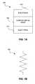
- FIG. 1Adepicts a block diagram of a resistive memory plug
- FIG. 1Bdepicts a schematic representation of the memory plug of FIG. 1A
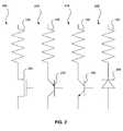
- FIG. 2depicts a schematic representation of various memory cells using a semiconductor device and the memory plug of FIG. 1B;
- FIG. 3Adepicts a schematic representation of a row of memory cells using a FET device, as shown in FIG. 2;
- FIG. 3Bdepicts a schematic representation of a row of memory cells using an alternate arrangement than that of FIG. 3A;
- FIG. 4depicts a schematic representation of an array of memory cells using the row arrangement of FIG. 3B;
- FIG. 5depicts a cross sectional diagram of a portion of the memory chip that implements the schematic layout of FIG. 4;
- FIG. 6depicts a cross sectional diagram of a partially formed cell after standard front end of line processes are completed
- FIG. 7depicts a cross sectional diagram of the partially formed cell of FIG. 6 after tungsten plug formation
- FIG. 8depicts a cross sectional diagram of the partially formed cell of FIG. 7 after the memory plugs are formed
- FIG. 9depicts a cross sectional diagram of the partially formed cell of FIG. 8 after the second set of W plugs are formed.
- FIG. 10depicts a cross sectional diagram of a completely formed cell.
- the present inventiongenerally allows for multi-resistive state materials to be used as memory elements in a non-volatile RAM memory.
- Multi-resistive state materialsgenerally require high temperature processing, which limits the types of material that can be used prior to the multi-resistive state material deposition.
- a non-volatile RAM chip that only uses materials that can withstand the high temperature processing below the multi-resistive state materialis free to use regular materials above the multi-resistive state material, since those materials are not subjected to high temperature processing.
- FIG. 1Adepicts a block diagram of a resistive memory plug 100 .
- the memory plug 100is typically made from a thin film of multi-resistive state material 105 placed between two electrodes 110 and 115 .
- the electrodes themselves 110 and 115are essentially passive to the operation of the memory plug, the interfaces between the electrodes 110 and 115 and the multi-resistive state material 105 may contribute to the resistive properties of the memory plug 100 .
- Electrodes 110 and 115should have significantly less resistance than the resistance of the multi-resistive state material 105 and should be of a constant resistance so as to not directly contribute to the electrical switching properties of the memory cell.
- electrodes 110 and 115would be as thin as possible while still preventing metal inter-diffusion and, if necessary, being useful as a seed layer and providing the active layer or layers.
- Typical electrodes 110 and 115 commonly used in fabricationinclude Pt, Au, Ag and Al. If the electrodes 110 and 115 are used only as a barrier to prevent metal inter-diffusion, then a thin layer of metal, e.g. TiN, could be used. If a seed layer is additionally required, any number of electrically conductive materials can be used for on top of the thin layer of metal.
- the seed layercould be a conductive perovskite, such as LaNiO 3 or SrRuO 3 on Pt, a conductive metal oxide, such as IrO 2 on Ir or RuO 2 on Ru, a noble metal such as Pt on TiN.
- the choice of electrode layers 110 , 115 in combination with the multi-resistive state material layer 105may affect the properties of the memory element.
- the memory functionis realized either by the multi-resistive state material 105 properties or by the interface between an electrode 110 or 115 and the multi-resistive state material 105 . Therefore all three layers 110 , 115 and 105 of the memory plug 100 can be considered as active layers.
- the multi-resistive state material 105will generally be a crystalline or polycrystalline structure.
- One class of multi-resistive state material 105are perovskites that include two or more metals, the metals being selected from the group consisting of transition metals, alkaline earth metals and rare earth metals.
- the perovskitescan be any number of compositions, including manganites (e.g., Pr 0.7 Ca 0.3 MnO 3 , Pr 0.5 Ca 0.5 MnO 3 and other PCMOs, LCMOs, etc.), titanates (e.g., STO:Cr), zirconates (e.g., SZO:Cr, Ca 2 Nb 2 O 7 :Cr, and Ta 2 O 5 :Cr), and high Tc superconductors (e.g., YBCO).
- manganitese.g., Pr 0.7 Ca 0.3 MnO 3 , Pr 0.5 Ca 0.5 MnO 3 and other PCMOs, LCMOs, etc.
- titanatese.g., STO:Cr
- zirconatese.g., SZO:Cr, Ca 2 Nb 2 O 7 :Cr, and Ta 2 O 5 :Cr
- high Tc superconductorse.g., YBCO
- MnO 3when combined with the rare earth metals La, Pr or some combination thereof and the alkaline earth metals Ca, Sr or some combination thereof have been found to produce a particularly effective multi-resistive state material 105 for use in the memory plug 100 .
- Multi-resistive state materials 105are not limited to perovskites. Specifically, any material that uses trapped charges to modify or alter conductivity could be used in the memory plug 100 . Doping different materials (e.g., insulators, conductors, conductive oxides, and/or polymers), for example, may create charge traps by substituting the dopant for crystalline elements. Doping may also be used to create charge traps by interstitially introducing dopants into a crystalline structure. Also, introducing separate physical clusters into a crystalline structure may additionally create charge traps.
- Doping different materialse.g., insulators, conductors, conductive oxides, and/or polymers
- Dopingmay also be used to create charge traps by interstitially introducing dopants into a crystalline structure. Also, introducing separate physical clusters into a crystalline structure may additionally create charge traps.
- the resistance changing effect of the multi-resistive state material 105is generally not dependent upon the area of the multi-resistive state material 105 or of its thickness. However, the resistance value is inversely proportional to the area of the thin film resistance and proportional to the thickness of the multi-resistive state material 105 . Additionally, the voltage at which multi-resistive state material 105 switches resistive states is dependent upon its thickness. The area and the thickness of the multi-resistive state material 105 as well as its resistivity will determine both the lowest possible resistance state and the highest possible resistive state.
- Sources of resistanceinclude the contacts and the vias, the metal interconnect lines, and the driver circuits.
- Parasitic resistancesmight total 100-200 ⁇ , which puts a lower limit on the value of the memory plug resistance. While the problem can be overcome through more complicated circuit design, such designs typically result in loss of access time. Additionally, if the memory plug resistance is too high, then the RC delays in the circuit will be long, increasing the access time.
- the R 1 state of the memory plugwould have a best value of 10 k ⁇ to 100 k ⁇ . However, workable values may also be achieved with resistances between 5 k ⁇ to 1 M ⁇ . If the R 1 state resistance is much less than 10 k ⁇ , access time will be increased because of the effect of the parasitic resistances. If the R 1 state value is much above 100 k ⁇ , the RC delays will increase access time.
- V Rread voltage
- R 1might be about 100 k ⁇ and R 0 might be about 1 M ⁇ , making the current either 10 ⁇ A or 1 ⁇ A, depending on the resistive state.
- V Wdesired write voltage
- V Wshould be greater than V Wth for the same reason.
- a typical V Wmight be about 2 volts, and V Wth might be about 1.5 volts.
- multi-resistive state material 105can be placed into several different resistive states, multi-bit resistive memory cells are possible.
- the multi-resistive state material materialmight have a high resistive state of R 00 , a medium-high resistive state of R 01 , a medium-low resistive state of R 11 and a low resistive state of R 11 .
- multi-bit memoriestypically have access times longer than single-bit memories
- using a factor greater than a 10 times change in resistance from R 11 to R 00is one way to make a multi-bit memory as fast as a single-bit memory.
- a memory cell that is capable of storing two bitsmight have the low resistive state be separated from the high resistive state by a factor of 100.
- a memory cell that is capable of storing three or four bits of informationmight require the low resistive state be separated from the high resistive state by a factor of 1000.
- the intermediary resistive states in a multi-bit memorywould evenly subdivide the resistive range between the high resistive state and the low resistive state on a logarithmic scale.
- the above-described voltagesare voltages seen by the multi-resistive state material 105 , and not necessarily the absolute values of the voltages from ground. For example, if the top electrode 110 was held to 10 volts and the bottom electrode 115 was held to 8 volts, the multi-resistive state material 105 would still attain a 2-volt drop. An opposite polarity voltage would then be attained whenever the bottom electrode 115 was held to a larger voltage than the top electrode 110 . Different designs might then use different methods to create a voltage drop of opposite polarity and equal magnitude.
- top electrode 110being held to 10 volts and the bottom electrode 115 being held to 8 volts
- one designmight hold the top electrode 110 to the same 10 and change only the voltage on the bottom electrode 115 to 12 volts in order to attain a voltage drop of opposite polarity and equal magnitude.
- An alternative designmight reverse the voltages on the electrodes, holding the bottom electrode 115 to 10 volts and the top electrode 110 to 8 volts so that neither electrode would experience a change in voltage of more than 2 volts.
- the multi-resistive state material 105should switch very quickly from one resistive state to another. For current applications, anything less than 50 nanoseconds would be an appropriate switching speed. Additionally, once the multi-resistive state material 105 is placed in a resistive state, it should be able to retain that state for long periods of time. Ideally, the material should retain its resistive state for over ten years. Since the read voltage should not affect the resistive state, repeated application of the read voltage over ten years should not change the resistive state of the multi-resistive state material 105 .
- the chemical and materials properties of the multi-resistive state material 105are selected to meet the electrical specifications set forth above.
- the materialpreferably has a resistivity of not greater than about 1 ⁇ -cm (although 5 ⁇ -cm may be a workable value), exhibits a change in resistance of at least about 10 ⁇ , and has this resistance change triggered by the application of a voltage pulse of not longer than about 100 ns duration and not greater than about than 10V in magnitude.
- the memory element materialshould be compatible with the requirements imposed by the general fabrication process of the entire high density RAM. Of course, there is some flexibility in the process constraints. Thus, process and design engineers will have certain ranges of chemical, materials, and process parameters available to tailor for the specific goals at hand. Among these parameters are the annealing conditions, the deposition temperature and method, and the material stoichiometry and the thickness.
- the memory element material resistivityshould be optimized.
- the resistivity of the multi-resistive state materialsdepends upon various factors, often including some of the following: film thickness, oxygen content of the film, stoichiometry, elemental composition, deposition method and conditions, degree of crystallinity, crystallite size, crystalline orientation, and doping level and choice of dopant.
- film thicknessoxygen content of the film
- stoichiometryelemental composition
- deposition method and conditionsdegree of crystallinity, crystallite size, crystalline orientation
- doping level and choice of dopantdoping level and choice of dopant.
- One example of a suitable film thickness for the memory applications of this inventionis approximately 500 ⁇ to 3000 ⁇ . Thinner films sometimes have higher strains, usually resulting from a slight misalignment with the seed layer, which can result in higher resistivity. Film thickness has been discussed by S. I. Khartsev, et al. in “Colossal magnetoresistance in ultrathin epitaxial La 0.75 Sr 0.25 MnO 3 films,” Journal of Applied Physics, Vol. 87, No. 5, 1 March 2000, which is hereby incorporated by reference for all purposes.
- Another factor that affects resistivityis the oxygen content of the film.
- the resistivitycan be controlled. It has been observed that 1500 ⁇ lanthanum manganese oxide (LMO) films deposited by pulsed laser deposition in oxygen environments have a lower resistivity than films deposited in vacuum (but otherwise identical conditions). See Y. G. Zhao, et al., “Effect of oxygen content on the structural, transport, and magnetic properties of La 1 ⁇ Mn 1 ⁇ thin films,” Journal of Applied Physics, Vol. 86, No. 11, 1 December 1999, which is hereby incorporated by reference for all purposes. Cooling down the freshly deposited film in an oxygen-containing atmosphere further decreases film resistivity.
- LMOlanthanum manganese oxide
- some specific multi-resistive state material materials suitable for use with this inventionwill have the following properties: (1) the thickness of the deposited multi-resistive state material film is between 500 ⁇ and 3000 ⁇ ; (2) the deposition and cool down and post deposition annealing (if any) is performed in an oxygen rich ambient; (3) the ratio of the rare earth and alkaline earth metals is adjusted for lowest resistivity, e.g., about 0.5; (4) the material is deposited or annealed to give a polycrystalline structure; (5) the material is deposited or annealed to increase the percentage of crystallites in a preferred orientation; and (6) the multi-resistive state material material is doped with a material that has the effect of pinning the oxygen vacancies and/or introducing trapping sites within the material, and/or altering the resistivity of the material.
- the seed layer or other “substrate” on which the multi-resistive state material depositsimpacts the resistivity of the multi-resistive state material and other properties.
- the underlying crystrallographic orientation of the substratewill epitaxially propagate to the upper levels the multi-resistive state material element. So, for example, if the underlying substrate has a 100 orientation, then the multi-resistive state material may preferentially deposit in a 100 orientation.
- the underlying substrateis a conductive electrode such a noble metal (e.g., platinum) or relatively conductive multi-resistive state material such as LaNiO 3 . In polycrystalline structures, suitable crystallite sizes may range from about 100 ⁇ to about 500 ⁇ .
- the general process operations for creating a multi-resistive state material memory pluginclude (1) providing a substrate on which to directly form the memory plug, (2) depositing the memory plug material on the substrate, and optionally (3) post-processing the deposited material to impart a desired property.
- the substrate materialshould be polycrystalline or single crystalline, be conductive, and serve as an electrode.
- PVDphysical vapor deposition
- CVDchemical vapor deposition
- FIG. 1Bis a schematic representation of the memory plug 100 .
- FIG. 2is a schematic representation of various memory cells 205 , 210 , 215 , and 220 using the memory plug 100 .
- the memory cells 205 , 210 , 215 , and 220all use a semiconductor device in order to control access to the memory plug 100 .
- Possible devicesinclude a FET 225 , a pnp transistor 230 , a npn transistor 235 , and a diode 240 .
- Other devicessuch as a parasitic vertical bipolar transistor that consists of a p junction and an N well in a p substrate, may also be used.
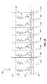
- FIG. 3Ais a schematic representation of an array 300 of memory cells 205 .
- Each memory cell 205 in the arrayis connected to a select line 305 , a reference line 310 and a plurality of data lines 315 , 320 , 325 , 330 , 335 , 340 , 345 , and 350 .
- Activating the FET 225requires a gate voltage that is above the threshold voltage of the FET 225 .
- the select line 305therefore, is used to activate all the FETs in a particular row of memory cells.
- the data lines 315 , 320 , 325 , 330 , 335 , 340 , 345 , and 350both carry the data from the memory cells during READ operation and provides the memory cells with a voltage pulse appropriate to change the resistive state of the memory plug 100 during a WRITE operation.
- Selection circuitrycan be used to select a specific data line 315 , 320 , 325 , 330 , 335 , 340 , 345 or 350 so that only the desired memory cells are accessed.
- the reference line 310provides a reference voltage to all the memory cells.
- the reference voltageis typically either ground (0V) or a constant supply voltage.
- more than one celle.g., 205 and 355
- one select line 305is active and more than one data line (e.g., 315 and 350 ) is active
- the resulting current from all the active data lines 315 and 350would go through the cells 205 and 355 to the common reference line 310 .
- Thismay be too much current for a single reference line 310 , and may result in a voltage drop due to the parasitic resistance, especially in a large array. It could also affect the reliability of the reference line 310 due to electro-migration induced by too much current in the line. Techniques that address this issue are discussed in connection with FIG. 4.
- FIG. 3Bis a schematic representation of an array 360 that has the memory cells flipped upside down so that the memory plug 100 is connected with the reference line 310 and the FET 225 is connected to the select line 305 and the appropriate data line 315 .
- the transistor 225is able to prevent the memory plug 100 from experiencing a voltage drop between the data line 315 and the reference line 310 .
- the array 300 of FIG. 3Awould still cause the memory plug 100 to experience voltage changes associated with the changing data line 315 , but no voltage drop.
- memory plug 100 in the configuration of FIG. 3Bis subjected to the constant voltage of the reference line 310 for as long as the transistor 225 is not activated.
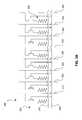
- FIG. 4is a schematic representation of an array 400 of memory cells laid out in a repeatable pattern in two dimensions. Although there are multiple select lines 405 , 410 , and 415 , and data lines 420 , 425 , 430 , and 435 , each individual memory cell 205 can be uniquely defined by a single select line 410 and a single data line 425 . Table 1 shows the operational voltages that could be applied to the array 400 in one possible embodiment of the invention.
- the reference lines 440 and 445stay grounded. As previously described, activating more than one cell at a time may lead to voltage drops due to parasitic resistances.
- One technique that can be used to avoid this problemis to tie all the reference lines (e.g., 440 and 445 ) together at regular intervals. For example, including a line parallel to the data lines every 64 cells might ameliorate any unwanted voltage drops. Regardless of the technique used, it would generally be desirable to keep the reference line at a constant voltage.
- V R ′V R plus all other incidental voltage drops of the memory cell, such as from the electrodes 110 and 115 and the FET 225 ).
- the voltage of the floating unselected data lines 420 , 430 , and 435must not, however, exceed
- the unselected data lines 420 , 430 , and 435might be held to some voltage in between V Wth ′ and ⁇ V Wth ′ (such as the reference voltage) if parasitic capacitance or some other correction mechanism was not thought to be sufficient to prevent the voltage from floating too high or too low.
- an unselected memory plug 465 along an unselected data line 435 and an unselected select line 415would have a gate voltage of ⁇ 2V, which is lower than both the unselected data line, which cannot float to less than ⁇ 2V, and the reference voltage, which is 0V.
- the WRITE 1 operationputs the memory plug 100 into the R 1 state. This can either be done only after a read to ensure that the memory plug 100 is not already in the R 1 state, or it can be done without a read if R 1 is the highest possible state.
- the WRITE 0 operationputs the memory plug 100 into the R 0 state, which is typically the lowest possible resistive state of the memory plug 100 .
- the unselected memory cellsare not affected by either WRITE operation either because their gates are not activated or the unselected data lines only float between voltages of V Wth ′ and ⁇ V Wth ′.
- two on chip voltage converterswill convert the chip power supply, typically 3V or 1.8V, to the required value.
- One voltage converterfor example, could produce a 2V signal, and the other might produce a ⁇ 2V signal.
- FIG. 5is a cross sectional diagram of a portion of the memory chip 500 that implements the schematic layout of FIG. 4. Three layers are used on top of the silicon wafer 505 : one for the select lines 405 , 410 , and 415 ; one for the reference line 440 ; and one for the data line 425 .
- the select lines 405 , 410 , and 415can be polysilicon or possibly silicide to provide a direct gate voltages for the n-channel FETs, allowing current to flow through two p-type junctions 510 and 515 when activated.
- Polysilicon and silicidehave resistances of 3 to 30 ⁇ / ⁇ where copper metal lines typically have resistances of less than 0.1 ⁇ / ⁇ . Therefore, certain embodiments may have the chip be much longer in the data line-direction than the select line-direction.
- the multi-resistive state material layer 105may require very high temperatures to form the required polycrystalline or a single crystalline structure.
- the fabrication temperaturemight require that substances such as polysilicon, silicide, and/or refractory metals be used for the layers that are formed below the memory plug 100 , such as the select lines 405 , 410 , and 415 and some vias 520 and 525 .
- a more standard conductive metale.g., copper
- a more standard conductive metalcan be used for the layers that come after the multi-resistive state material layer 105 , such as the reference line 440 , metal plugs 530 and 535 , vias 540 , 545 , 550 , and 555 , and the data line 425 .
- the metal plugs 530 and 535are used to connect the vias 540 and 545 that are formed below the reference line 440 metalization layer and the vias 550 and 555 that are formed above the reference line 440 metalization layer so that the data line 425 is connected to the p junctions 510 and 560 .
- FIG. 6- 10describe one possible technique that can be used to fabricate the cell 205 , using specific materials. It should be understood that the described materials, processes and thicknesses are not the only embodiment that can be used.
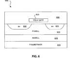
- FIG. 6is a cross sectional diagram of a partially formed cell 600 after standard front end of line (FEOL) processes are completed.
- FEOL processesare generally defined as operations performed on a semiconductor wafer in the course of device manufacturing up to first metallization, and might end with chemical-mechanical polishing (CMP) of SiO 2 as an inter-layer dielectric (ILD) 605 .
- CMPchemical-mechanical polishing
- FIG. 6shows a p-type substrate 610 , which lies beneath an n-well 615 , which, in turn, is underneath a p-well 620 .
- N-junctions 625 and 630are formed in the p-well 620 . Since the data lines may be at ⁇ 2V, the isolated p-well 620 allows the n-junctions 625 and 630 to always be reverse-biased, even at negative voltages.
- the select line 635can be formed as a standard polysilicon gate.
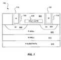
- FIG. 7is a cross sectional diagram of a partially formed cell 700 after tungsten (W) plug formation.
- Wtungsten
- the next processing stepis formation of contact holes through the ILD 605 .
- a barrier/adhesion layer 705 and 710 of 100 ⁇ of Ti followed by 200 ⁇ of TiNcan be sputtered on the wafer, followed by 5000 ⁇ of W, deposited using CVD, followed by etchback or CMP to remove W on the ILD 605 surface, leaving W plugs 715 and 720 in the contact holes.
- FIG. 8is a cross sectional diagram of a partially formed cell 800 after the memory plugs are formed.
- the bottom electrode 805is deposited.
- the bottom electrode 805can have two layers, a 500 ⁇ thick barrier layer of TiAIN to prevent metal inter-diffusion, followed by a 200 ⁇ seed layer of LaNiO 3 . These layers can be deposited by sputtering.
- 2000 ⁇ of memory material 810 having a stoichiometry of Pr 0.7 Ca 0.3 MnO 3can then be deposited at about 600° C. by a physical vapor deposition technique such as sputtering, and then annealed.
- the top electrode 815(200 ⁇ of SrRuO 3 and another 500 ⁇ of TiAIN) is deposited on top of the memory element 810 via sputtering.
- Standard photolithography and appropriate multi-step etch processescan then be used to pattern the electrode/memory/electrode layers into memory cell plug.
- 250 ⁇ of Si 3 N 4 or TiO 2might then be deposited as an etch stop/diffusion barrier 820 , to protect the PCMO film from inter-diffusion.
- FIG. 9is a cross sectional diagram of a partially formed cell 900 after the second set of W plugs are formed.
- a thick SiO 2 layer as a second ILD 905is deposited and planarized by CMP.
- the via holesare then formed with standard photolithography and via etch.
- the via holescould be filled by depositing a barrier/adhesion layer 910 and 915 of 100 ⁇ of Ti, followed by 200 ⁇ of TiN, followed by W plug layer 920 and 925 of 5000 ⁇ of W.
- CMPcould then be used to remove W on the ILD surface 905 , leaving the W plugs 920 and 925 in the via holes.
- FIG. 10is a cross sectional diagram of a completely formed cell 1000 .
- two metalization layerscan be formed above the partially formed cell 900 of FIG. 9.
- the first metalization layercan be used to form both the reference line 1005 and a metal pad 1010 , which eventually connects two tungsten plugs 920 and 1015 .
- the second tungsten plug 1015is used to connect the data line 1020 , which is formed during the second metalization layer, to the metal plug 1010 , through a third ILD 1025 , which is used to support the data line 1020 .
Landscapes
- Engineering & Computer Science (AREA)
- Chemical & Material Sciences (AREA)
- Materials Engineering (AREA)
- Computer Hardware Design (AREA)
- Semiconductor Memories (AREA)
Abstract
Description
- This application claims the benefit of U.S. Provisional Application No. 60/400,849, filed Aug. 2, 2002, and the U.S. Provisional Application No. 60/422,922, filed Oct. 31, 2002, both of which are incorporated herein by reference in their entireties and for all purposes. This application is related to the following U.S. Patent Applications: U.S. application Ser. No. 10/360,005, filed Feb. 7, 2003; U.S. application Ser. No. 10/330,512, filed Dec. 2326, 2002; application Ser. No. 10/330,153, filed Dec. 26, 2002; application Ser. No. 10/330,964, filed Dec. 26, 2002; application Ser. No. 10/330,170, filed Dec. 26, 2002; application Ser. No. 10/330,900, filed Dec. 26, 2002; application Ser. No. 10/330,150, filed Dec. 26, 2002; and application Ser. No. 10/330,965, filed Dec. 26, 2002; all of which are hereby incorporated herein by reference in their entireties and for all purposes. This application is additionally related to the U.S. Patent Applications titled “Memory Array of a Non-Volatile RAM” filed on date even herewith, hereby incorporated herein by reference in its entirety and for all purposes.[0001]
- 1. Field of the Invention[0002]
- The present invention relates generally to memory, and more specifically to nonvolatile RAM.[0003]
- 2. Description of the Related Art[0004]
- Memory can either be classified as volatile or nonvolatile. Volatile memory is memory that loses its contents when the power is turned off. Some solid-state memory devices do not require a continuous power supply to retain information.[0005]
- Certain complex metal oxides (CMOs), for example, can retain a resistive state after being exposed to an electronic pulse, which can be generated from two terminals. U.S. Pat. No. 6,204,139, issued Mar. 20, 2001 to Liu et al., incorporated herein by reference for all purposes, describes some perovskite materials that exhibit such characteristics. The perovskite materials are also described by the same researchers in “Electric-pulse-induced reversible resistance change effect in magnetoresistive films,” Applied Physics Letters, Vol. 76, No. 19, 8 May 2000, and “A New Concept for Non-Volatile Memory: The Electric-Pulse Induced Resistive Change Effect in Colossal Magnetoresistive Thin Films,”in materials for the 2001 Non-Volatile Memory Technology Symposium, all of which are hereby incorporated by reference for all purposes. However, the materials described in the 6,204,139 patent is not generally applicable to RAM memory because the resistance of the material, when scaled to small dimensions, is considered to be too large to make a memory with fast access times.[0006]
- Similarly, the IBM Zurich Research Center has also published three technical papers that also discuss the use of metal oxide material for memory applications: “Reproducible switching effect in thin oxide films for memory applications,” Applied Physics Letters, Vol. 77, No. 1, 3 July 2000, “Current-driven insulator-conductor transition and nonvolatile memory in chromium-doped SrTiO[0007]3single crystals,” Applied Physics Letters, Vol. 78, No. 23, 4 June 2001, and “Electric current distribution across a metal-insulator-metal structure during bistable switching,” Journal of Applied Physics, Vol. 90, No. 6, 15 September 2001, all of which are hereby incorporated by reference for all purposes.
- The discovery of the resistance-changing property of certain CMOs, however, is relatively recent and has not yet been implemented in a commercially viable memory product. There are continuing efforts to bring a true nvRAM to market.[0008]
- The present invention generally allows for non-volatile memory cell that retains information even if power ceases to be supplied to the memory cell. In one aspect, a non-volatile RAM memory array includes a plurality of memory cells formed on a semiconductor substrate, each individual cell capable of being selected with a select line and a data line. Each individual cell contains a semiconductor device and a multi-resistive state material.[0009]
- The semiconductor device controls current flow between the data line and the reference line depending on the voltage of the select line. Located between the data line and the reference line is the multi-resistive state material, which changes its resistive state from a high resistive state to a low resistive state upon application of a first voltage pulse across the multi-resistive state material and changes its resistive state from the low resistive state to the high resistive state upon application of a second voltage pulse across the multi-resistive state material. The second voltage pulse across the multi-resistive state material is of opposite polarity to the first voltage pulse. The resistive state of the multi-resistive state material then determines the information stored in the memory cell.[0010]
- In another aspect of the invention the semiconductor device is formed on a silicon substrate and two electrode layers are used. The multi-resistive state material layer is formed on the first electrode layer and the second electrode layer is formed on the multi-resistive state material, making a sandwich-like memory plug.[0011]
- The invention may best be understood by reference to the following description taken in conjunction with the accompanying drawings, in which:[0012]
- FIG. 1A depicts a block diagram of a resistive memory plug;[0013]
- FIG. 1B depicts a schematic representation of the memory plug of FIG. 1A;[0014]
- FIG. 2 depicts a schematic representation of various memory cells using a semiconductor device and the memory plug of FIG. 1B;[0015]
- FIG. 3A depicts a schematic representation of a row of memory cells using a FET device, as shown in FIG. 2;[0016]
- FIG. 3B depicts a schematic representation of a row of memory cells using an alternate arrangement than that of FIG. 3A;[0017]
- FIG. 4 depicts a schematic representation of an array of memory cells using the row arrangement of FIG. 3B;[0018]
- FIG. 5 depicts a cross sectional diagram of a portion of the memory chip that implements the schematic layout of FIG. 4;[0019]
- FIG. 6 depicts a cross sectional diagram of a partially formed cell after standard front end of line processes are completed;[0020]
- FIG. 7 depicts a cross sectional diagram of the partially formed cell of FIG. 6 after tungsten plug formation;[0021]
- FIG. 8 depicts a cross sectional diagram of the partially formed cell of FIG. 7 after the memory plugs are formed;[0022]
- FIG. 9 depicts a cross sectional diagram of the partially formed cell of FIG. 8 after the second set of W plugs are formed; and[0023]
- FIG. 10 depicts a cross sectional diagram of a completely formed cell.[0024]
- It is to be understood that, in the drawings, like reference numerals designate like structural elements. Also, it is understood that the depictions in the figures are not necessarily to scale.[0025]
- In the following description, numerous specific details are set forth to provide a thorough understanding of the present invention. It will be apparent, however, to one skilled in the art that the present invention may be practiced without some or all of these specific details. In other instances, well known process steps have not been described in detail in order to avoid unnecessarily obscuring the present invention.[0026]
- The present invention generally allows for multi-resistive state materials to be used as memory elements in a non-volatile RAM memory. Multi-resistive state materials generally require high temperature processing, which limits the types of material that can be used prior to the multi-resistive state material deposition. A non-volatile RAM chip that only uses materials that can withstand the high temperature processing below the multi-resistive state material is free to use regular materials above the multi-resistive state material, since those materials are not subjected to high temperature processing.[0027]
- FIG. 1A depicts a block diagram of a[0028]
resistive memory plug 100. Thememory plug 100 is typically made from a thin film ofmulti-resistive state material 105 placed between twoelectrodes electrodes multi-resistive state material 105 may contribute to the resistive properties of thememory plug 100.Electrodes multi-resistive state material 105 and should be of a constant resistance so as to not directly contribute to the electrical switching properties of the memory cell. Typically,electrodes - [0029]
Typical electrodes electrodes electrode layers state material layer 105 may affect the properties of the memory element. As such, the memory function is realized either by themulti-resistive state material 105 properties or by the interface between anelectrode multi-resistive state material 105. Therefore all threelayers memory plug 100 can be considered as active layers. - The[0030]
multi-resistive state material 105 will generally be a crystalline or polycrystalline structure. One class ofmulti-resistive state material 105 are perovskites that include two or more metals, the metals being selected from the group consisting of transition metals, alkaline earth metals and rare earth metals. The perovskites can be any number of compositions, including manganites (e.g., Pr0.7Ca0.3MnO3, Pr0.5Ca0.5MnO3and other PCMOs, LCMOs, etc.), titanates (e.g., STO:Cr), zirconates (e.g., SZO:Cr, Ca2Nb2O7:Cr, and Ta2O5:Cr), and high Tc superconductors (e.g., YBCO). Specifically, MnO3, when combined with the rare earth metals La, Pr or some combination thereof and the alkaline earth metals Ca, Sr or some combination thereof have been found to produce a particularly effectivemulti-resistive state material 105 for use in thememory plug 100. - [0031]
Multi-resistive state materials 105 are not limited to perovskites. Specifically, any material that uses trapped charges to modify or alter conductivity could be used in thememory plug 100. Doping different materials (e.g., insulators, conductors, conductive oxides, and/or polymers), for example, may create charge traps by substituting the dopant for crystalline elements. Doping may also be used to create charge traps by interstitially introducing dopants into a crystalline structure. Also, introducing separate physical clusters into a crystalline structure may additionally create charge traps. - The resistance changing effect of the[0032]
multi-resistive state material 105 is generally not dependent upon the area of themulti-resistive state material 105 or of its thickness. However, the resistance value is inversely proportional to the area of the thin film resistance and proportional to the thickness of themulti-resistive state material 105. Additionally, the voltage at whichmulti-resistive state material 105 switches resistive states is dependent upon its thickness. The area and the thickness of themulti-resistive state material 105 as well as its resistivity will determine both the lowest possible resistance state and the highest possible resistive state. Although the highest operational resistive state (R0) of thememory plug 100 does not need to be its highest possible state and the lowest operational resistance state (R1) does not need to be its lowest possible state, designs can set R0and R1close to those states for simplicity. - When considering an operative value of the R[0033]1resistive state parasitic resistances that are in series with the memory plug must also be considered. Sources of resistance include the contacts and the vias, the metal interconnect lines, and the driver circuits. Parasitic resistances might total 100-200 Ω, which puts a lower limit on the value of the memory plug resistance. While the problem can be overcome through more complicated circuit design, such designs typically result in loss of access time. Additionally, if the memory plug resistance is too high, then the RC delays in the circuit will be long, increasing the access time.
- Therefore, the R[0034]1state of the memory plug would have a best value of 10 kΩ to 100 kΩ. However, workable values may also be achieved with resistances between 5 kΩ to 1 MΩ. If the R1state resistance is much less than 10 kΩ, access time will be increased because of the effect of the parasitic resistances. If the R1state value is much above 100 kΩ, the RC delays will increase access time.
- Although very dramatic differences between a R[0035]1and R0could be sensed very easily, the voltage that drives very high resistances would be less than ideal. Since large currents can be destructive to semiconductors fabricated to small dimensions, no more than 10 μA would be desired for a memory circuit in most cases. Conversely, small differences, while workable in certain applications, result in difficulties in sensing the change in resistance and an increased access time. Typically, a single state memory would have the operational resistances of R0and R1separated by a factor of 10.
- For example, if 1 volt were used as a read voltage (V[0036]R), R1might be about 100 kΩ and R0might be about 1 MΩ, making the current either 10 μA or 1 μA, depending on the resistive state. Once a VRis identified, a desired write voltage (VW) can also be determined. Not only should VWbe greater than VR, but it should also be far enough away from VRto allow minor voltage fluctuations (e.g., due to fabrication imperfections) to have a negligible effect on the
multi-resistive state material 105. Similarly, VWshould be greater than VWthfor the same reason. A typical VWmight be about 2 volts, and VWthmight be about 1.5 volts. - However, it should be noted that changes greater than a factor of 10 might be desirable in multi-bit resistive memory cells. Generally, adjusting the pulse width and magnitude of the voltage pulses across the multi-resistive state material material results in multiple resistive states. Since[0037]
multi-resistive state material 105 can be placed into several different resistive states, multi-bit resistive memory cells are possible. For example, the multi-resistive state material material might have a high resistive state of R00, a medium-high resistive state of R01, a medium-low resistive state of R11and a low resistive state of R11. Since multi-bit memories typically have access times longer than single-bit memories, using a factor greater than a 10 times change in resistance from R11to R00is one way to make a multi-bit memory as fast as a single-bit memory. For example, a memory cell that is capable of storing two bits might have the low resistive state be separated from the high resistive state by a factor of 100. A memory cell that is capable of storing three or four bits of information might require the low resistive state be separated from the high resistive state by a factor of 1000. Typically, the intermediary resistive states in a multi-bit memory would evenly subdivide the resistive range between the high resistive state and the low resistive state on a logarithmic scale. For example, if a memory cell that held three bits of memory had a low resistive state of 10 kΩ, the six intermediary states might have resistive states of about 26.8 kΩ, 72.0 kΩ, 193 kΩ, 518 kΩ, 1.39 MΩ, and 3.73 MΩ. The highest resistive state would then be 10 MΩ, 1000 times the value of the low resistive state. Each optimal resistive state could easily be calculated by using the relationship Log(R110)=Log(R111)+Log K; Log(R101)=Log(R111)+2 Log K; Log(R100)=Log(R111)+3 Log K; . . . Log(R000)=Log(R111)+7 Log K, where Log K=({fraction (1/7)})[Log(R000)−Log(R111)]. - Those skilled in the art will appreciate that the above-described voltages are voltages seen by the[0038]
multi-resistive state material 105, and not necessarily the absolute values of the voltages from ground. For example, if thetop electrode 110 was held to 10 volts and thebottom electrode 115 was held to 8 volts, themulti-resistive state material 105 would still attain a 2-volt drop. An opposite polarity voltage would then be attained whenever thebottom electrode 115 was held to a larger voltage than thetop electrode 110. Different designs might then use different methods to create a voltage drop of opposite polarity and equal magnitude. Taking the example of thetop electrode 110 being held to 10 volts and thebottom electrode 115 being held to 8 volts, one design might hold thetop electrode 110 to the same 10 and change only the voltage on thebottom electrode 115 to 12 volts in order to attain a voltage drop of opposite polarity and equal magnitude. An alternative design might reverse the voltages on the electrodes, holding thebottom electrode 115 to 10 volts and thetop electrode 110 to 8 volts so that neither electrode would experience a change in voltage of more than 2 volts. - Ideally, the[0039]
multi-resistive state material 105 should switch very quickly from one resistive state to another. For current applications, anything less than 50 nanoseconds would be an appropriate switching speed. Additionally, once themulti-resistive state material 105 is placed in a resistive state, it should be able to retain that state for long periods of time. Ideally, the material should retain its resistive state for over ten years. Since the read voltage should not affect the resistive state, repeated application of the read voltage over ten years should not change the resistive state of themulti-resistive state material 105. - Generally, the chemical and materials properties of the[0040]
multi-resistive state material 105 are selected to meet the electrical specifications set forth above. For example, the material preferably has a resistivity of not greater than about 1 Ω-cm (although 5 Ω-cm may be a workable value), exhibits a change in resistance of at least about 10×, and has this resistance change triggered by the application of a voltage pulse of not longer than about 100 ns duration and not greater than about than 10V in magnitude. In addition, the memory element material should be compatible with the requirements imposed by the general fabrication process of the entire high density RAM. Of course, there is some flexibility in the process constraints. Thus, process and design engineers will have certain ranges of chemical, materials, and process parameters available to tailor for the specific goals at hand. Among these parameters are the annealing conditions, the deposition temperature and method, and the material stoichiometry and the thickness. - To allow rapid access times (on the order of tens of nanoseconds) in small dimension devices (on the order of hundreds of nanometers), the memory element material resistivity should be optimized. The resistivity of the multi-resistive state materials depends upon various factors, often including some of the following: film thickness, oxygen content of the film, stoichiometry, elemental composition, deposition method and conditions, degree of crystallinity, crystallite size, crystalline orientation, and doping level and choice of dopant. Current research indicates that suitably low resistivity multi-resistive state material materials can be achieved byjudicious choice of these parameters.[0041]
- One example of a suitable film thickness for the memory applications of this invention is approximately 500 Å to 3000 Å. Thinner films sometimes have higher strains, usually resulting from a slight misalignment with the seed layer, which can result in higher resistivity. Film thickness has been discussed by S. I. Khartsev, et al. in “Colossal magnetoresistance in ultrathin epitaxial La[0042]0.75Sr0.25MnO3films,” Journal of Applied Physics, Vol. 87, No. 5, 1 March 2000, which is hereby incorporated by reference for all purposes.
- Another factor that affects resistivity is the oxygen content of the film. By properly controlling the exposure to oxygen during deposition and annealing (if any) the resistivity can be controlled. It has been observed that 1500 Å lanthanum manganese oxide (LMO) films deposited by pulsed laser deposition in oxygen environments have a lower resistivity than films deposited in vacuum (but otherwise identical conditions). See Y. G. Zhao, et al., “Effect of oxygen content on the structural, transport, and magnetic properties of La[0043]1−δMn1−δ thin films,” Journal of Applied Physics, Vol. 86, No. 11, 1 December 1999, which is hereby incorporated by reference for all purposes. Cooling down the freshly deposited film in an oxygen-containing atmosphere further decreases film resistivity.
- It has been further observed that adjusting the relative amounts of the rare earths and the alkaline earth metals can modify resistivity. Higher ratios of alkaline earth to rare earth metals can, to a degree (e.g., up to about 50:50 in lanthanum calcium manganese oxides), lower resistivity. See Guo-Qiang Gong, et al., “Colossal magnetoresistance of 1000000-fold magnitude achieved in the antiferromagnetic phase of La[0044]1−xCaxMnO3,” Applied Physics Letters, Vol. 67, No. 12, 18 September 1995, which is hereby incorporated by reference for all purposes.
- Further, it has been found that some polycrystalline materials may have lower resistivities than their amorphous and single crystal counterparts. It has also been observed that magnitude of the resistance changes in single crystal multi-resistive state material films exceeds that of the polycrystalline films. Large changes (i.e., greater than about 10x), are, however, not typically necessary for making a practical memory chip.[0045]
- In light of the above, some specific multi-resistive state material materials suitable for use with this invention will have the following properties: (1) the thickness of the deposited multi-resistive state material film is between 500 Å and[0046]3000 Å; (2) the deposition and cool down and post deposition annealing (if any) is performed in an oxygen rich ambient; (3) the ratio of the rare earth and alkaline earth metals is adjusted for lowest resistivity, e.g., about 0.5; (4) the material is deposited or annealed to give a polycrystalline structure; (5) the material is deposited or annealed to increase the percentage of crystallites in a preferred orientation; and (6) the multi-resistive state material material is doped with a material that has the effect of pinning the oxygen vacancies and/or introducing trapping sites within the material, and/or altering the resistivity of the material.
- In addition to the above properties, certain process and design features are important. First, the seed layer or other “substrate” on which the multi-resistive state material deposits impacts the resistivity of the multi-resistive state material and other properties. Often the underlying crystrallographic orientation of the substrate will epitaxially propagate to the upper levels the multi-resistive state material element. So, for example, if the underlying substrate has a 100 orientation, then the multi-resistive state material may preferentially deposit in a 100 orientation. Preferably, the underlying substrate is a conductive electrode such a noble metal (e.g., platinum) or relatively conductive multi-resistive state material such as LaNiO[0047]3. In polycrystalline structures, suitable crystallite sizes may range from about 100 Å to about 500 Å.
- The general process operations for creating a multi-resistive state material memory plug include (1) providing a substrate on which to directly form the memory plug, (2) depositing the memory plug material on the substrate, and optionally (3) post-processing the deposited material to impart a desired property. As indicated above, the substrate material should be polycrystalline or single crystalline, be conductive, and serve as an electrode.[0048]
- Various physical vapor deposition (PVD) and chemical vapor deposition (CVD) techniques may be employed. Many forms of PVD and CVD can be employed, assuming that they operate at temperatures compatible with the overall device fabrication technology. Post-processing operations must also meet the temperature strictures of the technology. Often, this means that the deposition process should operate at temperatures below 600° C.[0049]
- FIG. 1B is a schematic representation of the[0050]
memory plug 100. To make a practical memory cell using aresistive memory plug 100, some type of semiconductor device should be placed in series with theresistive element 100. FIG. 2 is a schematic representation ofvarious memory cells memory plug 100. Thememory cells memory plug 100. Possible devices include aFET 225, apnp transistor 230, anpn transistor 235, and adiode 240. Other devices, such as a parasitic vertical bipolar transistor that consists of a p junction and an N well in a p substrate, may also be used. - FIG. 3A is a schematic representation of an[0051]
array 300 ofmemory cells 205. Eachmemory cell 205 in the array is connected to aselect line 305, areference line 310 and a plurality ofdata lines - Activating the[0052]
FET 225 requires a gate voltage that is above the threshold voltage of theFET 225. Theselect line 305, therefore, is used to activate all the FETs in a particular row of memory cells. - The data lines[0053]315,320,325,330,335,340,345, and350 both carry the data from the memory cells during READ operation and provides the memory cells with a voltage pulse appropriate to change the resistive state of the
memory plug 100 during a WRITE operation. Selection circuitry can be used to select aspecific data line - The[0054]
reference line 310 provides a reference voltage to all the memory cells. The reference voltage is typically either ground (0V) or a constant supply voltage. In the case where more than one cell (e.g.,205 and355) is selected at a time, and where oneselect line 305 is active and more than one data line (e.g.,315 and350) is active, the resulting current from all theactive data lines cells common reference line 310. This may be too much current for asingle reference line 310, and may result in a voltage drop due to the parasitic resistance, especially in a large array. It could also affect the reliability of thereference line 310 due to electro-migration induced by too much current in the line. Techniques that address this issue are discussed in connection with FIG. 4. - The[0055]
array 300 of FIG. 3A is subject to numerous modifications. For example, FIG. 3B is a schematic representation of anarray 360 that has the memory cells flipped upside down so that thememory plug 100 is connected with thereference line 310 and theFET 225 is connected to theselect line 305 and theappropriate data line 315. - In both configurations the[0056]
transistor 225 is able to prevent thememory plug 100 from experiencing a voltage drop between thedata line 315 and thereference line 310. However, thearray 300 of FIG. 3A would still cause thememory plug 100 to experience voltage changes associated with the changingdata line 315, but no voltage drop. In contrast,memory plug 100 in the configuration of FIG. 3B is subjected to the constant voltage of thereference line 310 for as long as thetransistor 225 is not activated. - Similarly, FIG. 4 is a schematic representation of an[0057]
array 400 of memory cells laid out in a repeatable pattern in two dimensions. Although there are multipleselect lines data lines individual memory cell 205 can be uniquely defined by a singleselect line 410 and asingle data line 425. Table 1 shows the operational voltages that could be applied to thearray 400 in one possible embodiment of the invention.TABLE 1 Refer- Selected Unselected Selected Unselected ence Data Line Data Line Select Line Select Line Line Read 1 V Floating 3 V −2 V 0 V Write 1 −2 V Floating 3 V −2 V 0 V Write 0 2 V Floating 3 V −2 V 0 V - In the embodiment of table 1, the[0058]
reference lines - During the READ operation, the selected[0059]
memory plug 100 experiences a voltage drop of VR′(VR′ is VRplus all other incidental voltage drops of the memory cell, such as from theelectrodes - It should be noted that current also flows through the unselected memory plugs along the selected[0060]
select line 410. Anunselected memory plug 450 along the selectedselect line 410 would have its n-channel FET 455 active, allowing current to flow. However, since the decoding circuitry only reads information off of the selecteddata line 425, the current that flows through theunselected data lines memory cell 205. The voltage of the floatingunselected data lines electrodes 110 and115) or else the floating voltages may alter the resistive states in the unselected memory cells. Alternatively, theunselected data lines - Current does not flow through the other unselected memory plugs because their n-channel FETs do not have a gate voltage greater than the required threshold gate voltages. An[0061]
unselected memory cell 460 along the selecteddata line 425 would have a gate voltage of −2V, which is lower than both the voltage of the selecteddata line 425, which is 1V, and the reference voltage, which is 0V. Of course, any value of 0V or less could be used for the unselectedselect lines unselected memory plug 465 along anunselected data line 435 and an unselectedselect line 415 would have a gate voltage of −2V, which is lower than both the unselected data line, which cannot float to less than −2V, and the reference voltage, which is 0V. - The WRITE 1 operation puts the[0062]
memory plug 100 into the R1state. This can either be done only after a read to ensure that thememory plug 100 is not already in the R1state, or it can be done without a read if R1is the highest possible state. Similarly, the WRITE 0 operation puts thememory plug 100 into the R0state, which is typically the lowest possible resistive state of thememory plug 100. The unselected memory cells are not affected by either WRITE operation either because their gates are not activated or the unselected data lines only float between voltages of VWth′ and −VWth′. - To generate internal write voltages, two on chip voltage converters will convert the chip power supply, typically 3V or 1.8V, to the required value. One voltage converter, for example, could produce a 2V signal, and the other might produce a −2V signal.[0063]
- FIG. 5 is a cross sectional diagram of a portion of the[0064]
memory chip 500 that implements the schematic layout of FIG. 4. Three layers are used on top of the silicon wafer505: one for theselect lines reference line 440; and one for thedata line 425. Theselect lines type junctions - Polysilicon and silicide have resistances of 3 to 30 Ω/□ where copper metal lines typically have resistances of less than 0.1 Ω/□. Therefore, certain embodiments may have the chip be much longer in the data line-direction than the select line-direction.[0065]
- As previously discussed, the multi-resistive[0066]
state material layer 105 may require very high temperatures to form the required polycrystalline or a single crystalline structure. Depending upon the fabrication process (e.g., solution based spin on followed by high temperature anneal, pulsed laser deposition, sputtering, and metalorganic chemical vapor deposition) the fabrication temperature might require that substances such as polysilicon, silicide, and/or refractory metals be used for the layers that are formed below thememory plug 100, such as theselect lines vias state material layer 105 is deposited, a more standard conductive metal (e.g., copper) can be used for the layers that come after the multi-resistivestate material layer 105, such as thereference line 440, metal plugs530 and535, vias540,545,550, and555, and thedata line 425. The metal plugs530 and535 are used to connect thevias reference line 440 metalization layer and thevias reference line 440 metalization layer so that thedata line 425 is connected to thep junctions - FIG. 6-[0067]10 describe one possible technique that can be used to fabricate the
cell 205, using specific materials. It should be understood that the described materials, processes and thicknesses are not the only embodiment that can be used. - FIG. 6 is a cross sectional diagram of a partially formed[0068]
cell 600 after standard front end of line (FEOL) processes are completed. FEOL processes are generally defined as operations performed on a semiconductor wafer in the course of device manufacturing up to first metallization, and might end with chemical-mechanical polishing (CMP) of SiO2as an inter-layer dielectric (ILD)605. - FIG. 6 shows a p-[0069]
type substrate 610, which lies beneath an n-well615, which, in turn, is underneath a p-well 620. N-junctions junctions select line 635 can be formed as a standard polysilicon gate. - FIG. 7 is a cross sectional diagram of a partially formed[0070]
cell 700 after tungsten (W) plug formation. After the FEOL process, the next processing step is formation of contact holes through theILD 605. A barrier/adhesion layer ILD 605 surface, leaving W plugs715 and720 in the contact holes. - FIG. 8 is a cross sectional diagram of a partially formed[0071]
cell 800 after the memory plugs are formed. First, thebottom electrode 805 is deposited. Thebottom electrode 805 can have two layers, a 500 Å thick barrier layer of TiAIN to prevent metal inter-diffusion, followed by a 200 Å seed layer of LaNiO3. These layers can be deposited by sputtering. - 2000 Å of[0072]
memory material 810 having a stoichiometry of Pr0.7Ca0.3MnO3can then be deposited at about 600° C. by a physical vapor deposition technique such as sputtering, and then annealed. The top electrode815 (200 Å of SrRuO3and another 500 Å of TiAIN) is deposited on top of thememory element 810 via sputtering. Standard photolithography and appropriate multi-step etch processes can then be used to pattern the electrode/memory/electrode layers into memory cell plug. 250 Å of Si3N4or TiO2might then be deposited as an etch stop/diffusion barrier 820, to protect the PCMO film from inter-diffusion. - FIG. 9 is a cross sectional diagram of a partially formed[0073]
cell 900 after the second set of W plugs are formed. After the memory plug is fully formed, a thick SiO2layer as asecond ILD 905 is deposited and planarized by CMP. The via holes are then formed with standard photolithography and via etch. The via holes could be filled by depositing a barrier/adhesion layer W plug layer ILD surface 905, leaving the W plugs920 and925 in the via holes. - FIG. 10 is a cross sectional diagram of a completely formed[0074]
cell 1000. Using standard processes, two metalization layers can be formed above the partially formedcell 900 of FIG. 9. The first metalization layer can be used to form both thereference line 1005 and ametal pad 1010, which eventually connects two tungsten plugs920 and1015. Thesecond tungsten plug 1015 is used to connect thedata line 1020, which is formed during the second metalization layer, to themetal plug 1010, through athird ILD 1025, which is used to support thedata line 1020. - Although the invention has been described in its presently contemplated best mode, it is clear that it is susceptible to numerous modifications, modes of operation and embodiments, all within the ability and skill of those familiar with the art and without exercise of further inventive activity. For example, the polarity of the read voltage could be alternated with each read or a n-channel device can be replaced by a p-channel device. Accordingly, that which is intended to be protected by Letters Patent is set forth in the claims and includes all variations and modifications that fall within the spirit and scope of the claim.[0075]
Claims (46)
Priority Applications (6)
| Application Number | Priority Date | Filing Date | Title |
|---|---|---|---|
| US10/249,848US6856536B2 (en) | 2002-08-02 | 2003-05-12 | Non-volatile memory with a single transistor and resistive memory element |
| US10/605,977US7186569B2 (en) | 2002-08-02 | 2003-11-11 | Conductive memory stack with sidewall |
| US11/714,555US7528405B2 (en) | 2002-08-02 | 2007-03-05 | Conductive memory stack with sidewall |
| US12/283,339US7884349B2 (en) | 2002-08-02 | 2008-09-11 | Selection device for re-writable memory |
| US12/387,070US7847330B2 (en) | 2002-08-02 | 2009-04-27 | Four vertically stacked memory layers in a non-volatile re-writeable memory device |
| US12/928,239US20110080767A1 (en) | 2002-08-02 | 2010-12-06 | Integrated circuit including four layers of vertically stackedembedded re-writeable non-volatile two-terminal memory |
Applications Claiming Priority (3)
| Application Number | Priority Date | Filing Date | Title |
|---|---|---|---|
| US40084902P | 2002-08-02 | 2002-08-02 | |
| US42292202P | 2002-10-31 | 2002-10-31 | |
| US10/249,848US6856536B2 (en) | 2002-08-02 | 2003-05-12 | Non-volatile memory with a single transistor and resistive memory element |
Related Parent Applications (1)
| Application Number | Title | Priority Date | Filing Date |
|---|---|---|---|
| US10/605,963DivisionUS7009235B2 (en) | 2002-08-02 | 2003-11-10 | Conductive memory stack with non-uniform width |
Related Child Applications (2)
| Application Number | Title | Priority Date | Filing Date |
|---|---|---|---|
| US10/605,963Continuation-In-PartUS7009235B2 (en) | 2002-08-02 | 2003-11-10 | Conductive memory stack with non-uniform width |
| US10/605,977Continuation-In-PartUS7186569B2 (en) | 2002-08-02 | 2003-11-11 | Conductive memory stack with sidewall |
Publications (2)
| Publication Number | Publication Date |
|---|---|
| US20040160817A1true US20040160817A1 (en) | 2004-08-19 |
| US6856536B2 US6856536B2 (en) | 2005-02-15 |
Family
ID=32854239
Family Applications (1)
| Application Number | Title | Priority Date | Filing Date |
|---|---|---|---|
| US10/249,848Expired - LifetimeUS6856536B2 (en) | 2002-08-02 | 2003-05-12 | Non-volatile memory with a single transistor and resistive memory element |
Country Status (1)
| Country | Link |
|---|---|
| US (1) | US6856536B2 (en) |
Cited By (24)
| Publication number | Priority date | Publication date | Assignee | Title |
|---|---|---|---|---|
| US20040235200A1 (en)* | 2003-05-21 | 2004-11-25 | Sharp Laboratories Of America, Inc. | Oxygen content system and method for controlling memory resistance properties |
| EP1424697A3 (en)* | 2002-11-26 | 2005-03-16 | Sharp Kabushiki Kaisha | Common bit/common source line high density 1T1R resistive-ram array |
| US20060250837A1 (en)* | 2005-05-09 | 2006-11-09 | Sandisk 3D, Llc | Nonvolatile memory cell comprising a diode and a resistance-switching material |
| US20060250836A1 (en)* | 2005-05-09 | 2006-11-09 | Matrix Semiconductor, Inc. | Rewriteable memory cell comprising a diode and a resistance-switching material |
| US20060273298A1 (en)* | 2005-06-02 | 2006-12-07 | Matrix Semiconductor, Inc. | Rewriteable memory cell comprising a transistor and resistance-switching material in series |
| US20070029606A1 (en)* | 2005-08-04 | 2007-02-08 | Samsung Electronics Co., Ltd. | Phase change material, phase change random access memory including the same, and methods of manufacturing and operating the same |
| US20070070682A1 (en)* | 2005-09-12 | 2007-03-29 | Chieko Nakashima | Storage device and semiconductor device |
| US20070114509A1 (en)* | 2005-11-23 | 2007-05-24 | Sandisk 3D Llc | Memory cell comprising nickel-cobalt oxide switching element |
| US20070228414A1 (en)* | 2006-03-31 | 2007-10-04 | Sandisk 3D, Llc | Heterojunction device comprising a semiconductor and a resistivity-switching oxide or nitride |
| US20070236981A1 (en)* | 2006-03-31 | 2007-10-11 | Sandisk 3D, Llc | Multilevel nonvolatile memory cell comprising a resistivity-switching oxide or nitride and an antifuse |
| US20090001342A1 (en)* | 2007-06-29 | 2009-01-01 | April Schricker | Memory cell that employs a selectively grown reversible resistance-switching element and methods of forming the same |
| US20090001343A1 (en)* | 2007-06-29 | 2009-01-01 | April Schricker | Memory cell that employs a selectively deposited reversible resistance-switching element and methods of forming the same |
| US20090001344A1 (en)* | 2007-06-29 | 2009-01-01 | April Schricker | Memory cell that employs a selectively grown reversible resistance-switching element and methods of forming the same |
| US7495951B1 (en)* | 2006-04-27 | 2009-02-24 | Spansion Llc | Resistive memory cell array with common plate |
| US7521705B2 (en) | 2005-08-15 | 2009-04-21 | Micron Technology, Inc. | Reproducible resistance variable insulating memory devices having a shaped bottom electrode |
| US20090275169A1 (en)* | 2008-04-07 | 2009-11-05 | Hyun-Jun Sim | Semiconductor devices and methods of forming the same |
| US7829875B2 (en) | 2006-03-31 | 2010-11-09 | Sandisk 3D Llc | Nonvolatile rewritable memory cell comprising a resistivity-switching oxide or nitride and an antifuse |
| US7846785B2 (en) | 2007-06-29 | 2010-12-07 | Sandisk 3D Llc | Memory cell that employs a selectively deposited reversible resistance-switching element and methods of forming the same |
| US7932548B2 (en) | 2006-07-14 | 2011-04-26 | 4D-S Pty Ltd. | Systems and methods for fabricating self-aligned memory cell |
| US20120012897A1 (en)* | 2010-07-16 | 2012-01-19 | Unity Semiconductor Corporation | Vertically Fabricated BEOL Non-Volatile Two-Terminal Cross-Trench Memory Array with Two-Terminal Memory Elements and Method of Fabricating the Same |
| US8308915B2 (en) | 2006-09-14 | 2012-11-13 | 4D-S Pty Ltd. | Systems and methods for magnetron deposition |
| US8395199B2 (en) | 2006-03-25 | 2013-03-12 | 4D-S Pty Ltd. | Systems and methods for fabricating self-aligned memory cell |
| US8454810B2 (en) | 2006-07-14 | 2013-06-04 | 4D-S Pty Ltd. | Dual hexagonal shaped plasma source |
| CN109427792A (en)* | 2017-08-24 | 2019-03-05 | 美光科技公司 | Cross point memory array of structures and the method for forming cross point memory array of structures |
Families Citing this family (62)
| Publication number | Priority date | Publication date | Assignee | Title |
|---|---|---|---|---|
| US6859382B2 (en)* | 2002-08-02 | 2005-02-22 | Unity Semiconductor Corporation | Memory array of a non-volatile ram |
| US6753561B1 (en) | 2002-08-02 | 2004-06-22 | Unity Semiconductor Corporation | Cross point memory array using multiple thin films |
| US6970375B2 (en)* | 2002-08-02 | 2005-11-29 | Unity Semiconductor Corporation | Providing a reference voltage to a cross point memory array |
| US6917539B2 (en)* | 2002-08-02 | 2005-07-12 | Unity Semiconductor Corporation | High-density NVRAM |
| US7009235B2 (en)* | 2003-11-10 | 2006-03-07 | Unity Semiconductor Corporation | Conductive memory stack with non-uniform width |
| US7186569B2 (en)* | 2002-08-02 | 2007-03-06 | Unity Semiconductor Corporation | Conductive memory stack with sidewall |
| US6831854B2 (en)* | 2002-08-02 | 2004-12-14 | Unity Semiconductor Corporation | Cross point memory array using distinct voltages |
| US7057914B2 (en)* | 2002-08-02 | 2006-06-06 | Unity Semiconductor Corporation | Cross point memory array with fast access time |
| US6906939B2 (en)* | 2002-08-02 | 2005-06-14 | Unity Semiconductor Corporation | Re-writable memory with multiple memory layers |
| US7158397B2 (en)* | 2002-08-02 | 2007-01-02 | Unity Semiconductor Corporation | Line drivers that fits within a specified line pitch |
| US6940744B2 (en)* | 2002-10-31 | 2005-09-06 | Unity Semiconductor Corporation | Adaptive programming technique for a re-writable conductive memory device |
| US7309616B2 (en)* | 2003-03-13 | 2007-12-18 | Unity Semiconductor Corporation | Laser annealing of complex metal oxides (CMO) memory materials for non-volatile memory integrated circuits |
| US7029924B2 (en)* | 2003-09-05 | 2006-04-18 | Sharp Laboratories Of America, Inc. | Buffered-layer memory cell |
| US6962648B2 (en)* | 2003-09-15 | 2005-11-08 | Global Silicon Net Corp. | Back-biased face target sputtering |
| US7881133B2 (en) | 2003-11-11 | 2011-02-01 | Samsung Electronics Co., Ltd. | Method of managing a flash memory and the flash memory |
| US7099179B2 (en)* | 2003-12-22 | 2006-08-29 | Unity Semiconductor Corporation | Conductive memory array having page mode and burst mode write capability |
| EP1726017A1 (en)* | 2003-12-26 | 2006-11-29 | Matsushita Electric Industries Co., Ltd. | Memory device, memory circuit and semiconductor integrated circuit having variable resistance |
| US20060171200A1 (en) | 2004-02-06 | 2006-08-03 | Unity Semiconductor Corporation | Memory using mixed valence conductive oxides |
| US7082052B2 (en) | 2004-02-06 | 2006-07-25 | Unity Semiconductor Corporation | Multi-resistive state element with reactive metal |
| US7538338B2 (en)* | 2004-09-03 | 2009-05-26 | Unity Semiconductor Corporation | Memory using variable tunnel barrier widths |
| WO2005106892A1 (en)* | 2004-04-21 | 2005-11-10 | Micron Technology, Inc. | Sense amplifier for a non-volatile memory device |
| ITRM20040199A1 (en)* | 2004-04-21 | 2004-07-21 | Micron Technology Inc | DETECTION AMPLIFIER FOR A NON-VOLATILE MEMORY DEVICE. |
| US6972985B2 (en)* | 2004-05-03 | 2005-12-06 | Unity Semiconductor Corporation | Memory element having islands |
| US7330370B2 (en)* | 2004-07-20 | 2008-02-12 | Unity Semiconductor Corporation | Enhanced functionality in a two-terminal memory array |
| US7075817B2 (en) | 2004-07-20 | 2006-07-11 | Unity Semiconductor Corporation | Two terminal memory array having reference cells |
| JP2006099866A (en)* | 2004-09-29 | 2006-04-13 | Sony Corp | Storage device and semiconductor device |
| US20060081466A1 (en)* | 2004-10-15 | 2006-04-20 | Makoto Nagashima | High uniformity 1-D multiple magnet magnetron source |
| JP2006127583A (en)* | 2004-10-26 | 2006-05-18 | Elpida Memory Inc | Nonvolatile semiconductor memory device and phase change memory |
| US7464621B2 (en)* | 2004-11-09 | 2008-12-16 | Steeda Autosports, Inc. | Longitudinally displaced shifter |
| US7701834B2 (en)* | 2005-01-18 | 2010-04-20 | Unity Semiconductor Corporation | Movable terminal in a two terminal memory array |
| US20130082232A1 (en) | 2011-09-30 | 2013-04-04 | Unity Semiconductor Corporation | Multi Layered Conductive Metal Oxide Structures And Methods For Facilitating Enhanced Performance Characteristics Of Two Terminal Memory Cells |
| KR100724528B1 (en) | 2005-04-04 | 2007-06-04 | 한국과학기술연구원 | Thin film structure for resistance change memory device and manufacturing method |
| JP4475174B2 (en)* | 2005-06-09 | 2010-06-09 | ソニー株式会社 | Storage device |
| US7362604B2 (en)* | 2005-07-11 | 2008-04-22 | Sandisk 3D Llc | Apparatus and method for programming an array of nonvolatile memory cells including switchable resistor memory elements |
| US7345907B2 (en) | 2005-07-11 | 2008-03-18 | Sandisk 3D Llc | Apparatus and method for reading an array of nonvolatile memory cells including switchable resistor memory elements |
| US20070084716A1 (en)* | 2005-10-16 | 2007-04-19 | Makoto Nagashima | Back-biased face target sputtering based high density non-volatile data storage |
| US20070084717A1 (en)* | 2005-10-16 | 2007-04-19 | Makoto Nagashima | Back-biased face target sputtering based high density non-volatile caching data storage |
| US7816659B2 (en)* | 2005-11-23 | 2010-10-19 | Sandisk 3D Llc | Devices having reversible resistivity-switching metal oxide or nitride layer with added metal |
| KR101239962B1 (en)* | 2006-05-04 | 2013-03-06 | 삼성전자주식회사 | Variable resistive memory device comprising buffer layer on lower electrode |
| US7522468B2 (en)* | 2006-06-08 | 2009-04-21 | Unity Semiconductor Corporation | Serial memory interface |
| US7747817B2 (en)* | 2006-06-28 | 2010-06-29 | Unity Semiconductor Corporation | Performing data operations using non-volatile third dimension memory |
| US20080011603A1 (en)* | 2006-07-14 | 2008-01-17 | Makoto Nagashima | Ultra high vacuum deposition of PCMO material |
| US7719874B2 (en)* | 2006-07-31 | 2010-05-18 | Sandisk 3D Llc | Systems for controlled pulse operations in non-volatile memory |
| US7522448B2 (en)* | 2006-07-31 | 2009-04-21 | Sandisk 3D Llc | Controlled pulse operations in non-volatile memory |
| US7492630B2 (en)* | 2006-07-31 | 2009-02-17 | Sandisk 3D Llc | Systems for reverse bias trim operations in non-volatile memory |
| US7542338B2 (en)* | 2006-07-31 | 2009-06-02 | Sandisk 3D Llc | Method for reading a multi-level passive element memory cell array |
| US8279704B2 (en)* | 2006-07-31 | 2012-10-02 | Sandisk 3D Llc | Decoder circuitry providing forward and reverse modes of memory array operation and method for biasing same |
| US7499304B2 (en)* | 2006-07-31 | 2009-03-03 | Sandisk 3D Llc | Systems for high bandwidth one time field-programmable memory |
| US7542337B2 (en)* | 2006-07-31 | 2009-06-02 | Sandisk 3D Llc | Apparatus for reading a multi-level passive element memory cell array |
| US7499355B2 (en)* | 2006-07-31 | 2009-03-03 | Sandisk 3D Llc | High bandwidth one time field-programmable memory |
| US7495947B2 (en)* | 2006-07-31 | 2009-02-24 | Sandisk 3D Llc | Reverse bias trim operations in non-volatile memory |
| US7619945B2 (en)* | 2006-08-18 | 2009-11-17 | Unity Semiconductor Corporation | Memory power management |
| US7539811B2 (en) | 2006-10-05 | 2009-05-26 | Unity Semiconductor Corporation | Scaleable memory systems using third dimension memory |
| US7372753B1 (en)* | 2006-10-19 | 2008-05-13 | Unity Semiconductor Corporation | Two-cycle sensing in a two-terminal memory array having leakage current |
| US7379364B2 (en)* | 2006-10-19 | 2008-05-27 | Unity Semiconductor Corporation | Sensing a signal in a two-terminal memory array having leakage current |
| US8085615B2 (en) | 2006-12-29 | 2011-12-27 | Spansion Llc | Multi-state resistance changing memory with a word line driver for applying a same program voltage to the word line |
| US7765380B2 (en)* | 2007-01-19 | 2010-07-27 | Unity Semiconductor Corporation | Fast data access through page manipulation |
| US7663134B2 (en)* | 2007-07-10 | 2010-02-16 | Taiwan Semiconductor Manufacturing Company, Ltd. | Memory array with a selector connected to multiple resistive cells |
| US8208284B2 (en)* | 2008-03-07 | 2012-06-26 | Unity Semiconductor Corporation | Data retention structure for non-volatile memory |
| US8304754B2 (en)* | 2008-11-12 | 2012-11-06 | Sandisk 3D Llc | Metal oxide materials and electrodes for Re-RAM |
| US8233309B2 (en)* | 2009-10-26 | 2012-07-31 | Sandisk 3D Llc | Non-volatile memory array architecture incorporating 1T-1R near 4F2 memory cell |
| US9275731B1 (en)* | 2012-10-05 | 2016-03-01 | Marvell International Ltd. | Systems and methods for increasing the read sensitivity of a resistive random access memory (RRAM) |
Citations (10)
| Publication number | Priority date | Publication date | Assignee | Title |
|---|---|---|---|---|
| US5946227A (en)* | 1998-07-20 | 1999-08-31 | Motorola, Inc. | Magnetoresistive random access memory with shared word and digit lines |
| US6055178A (en)* | 1998-12-18 | 2000-04-25 | Motorola, Inc. | Magnetic random access memory with a reference memory array |
| US6097625A (en)* | 1998-07-16 | 2000-08-01 | International Business Machines Corporation | Magnetic random access memory (MRAM) array with magnetic tunnel junction (MTJ) cells and remote diodes |
| US6111781A (en)* | 1998-08-03 | 2000-08-29 | Motorola, Inc. | Magnetic random access memory array divided into a plurality of memory banks |
| US6178131B1 (en)* | 1999-01-11 | 2001-01-23 | Ball Semiconductor, Inc. | Magnetic random access memory |
| US6191972B1 (en)* | 1999-04-30 | 2001-02-20 | Nec Corporation | Magnetic random access memory circuit |
| US6204139B1 (en)* | 1998-08-25 | 2001-03-20 | University Of Houston | Method for switching the properties of perovskite materials used in thin film resistors |
| US6478106B2 (en)* | 2000-06-27 | 2002-11-12 | Dr. Ing. H.C.F. Porsche Ag | Device for forced guiding of a motor and/or powertrain with a crash case |
| US6531371B2 (en)* | 2001-06-28 | 2003-03-11 | Sharp Laboratories Of America, Inc. | Electrically programmable resistance cross point memory |
| US6731528B2 (en)* | 2002-05-03 | 2004-05-04 | Micron Technology, Inc. | Dual write cycle programmable conductor memory system and method of operation |
- 2003
- 2003-05-12USUS10/249,848patent/US6856536B2/ennot_activeExpired - Lifetime
Patent Citations (10)
| Publication number | Priority date | Publication date | Assignee | Title |
|---|---|---|---|---|
| US6097625A (en)* | 1998-07-16 | 2000-08-01 | International Business Machines Corporation | Magnetic random access memory (MRAM) array with magnetic tunnel junction (MTJ) cells and remote diodes |
| US5946227A (en)* | 1998-07-20 | 1999-08-31 | Motorola, Inc. | Magnetoresistive random access memory with shared word and digit lines |
| US6111781A (en)* | 1998-08-03 | 2000-08-29 | Motorola, Inc. | Magnetic random access memory array divided into a plurality of memory banks |
| US6204139B1 (en)* | 1998-08-25 | 2001-03-20 | University Of Houston | Method for switching the properties of perovskite materials used in thin film resistors |
| US6055178A (en)* | 1998-12-18 | 2000-04-25 | Motorola, Inc. | Magnetic random access memory with a reference memory array |
| US6178131B1 (en)* | 1999-01-11 | 2001-01-23 | Ball Semiconductor, Inc. | Magnetic random access memory |
| US6191972B1 (en)* | 1999-04-30 | 2001-02-20 | Nec Corporation | Magnetic random access memory circuit |
| US6478106B2 (en)* | 2000-06-27 | 2002-11-12 | Dr. Ing. H.C.F. Porsche Ag | Device for forced guiding of a motor and/or powertrain with a crash case |
| US6531371B2 (en)* | 2001-06-28 | 2003-03-11 | Sharp Laboratories Of America, Inc. | Electrically programmable resistance cross point memory |
| US6731528B2 (en)* | 2002-05-03 | 2004-05-04 | Micron Technology, Inc. | Dual write cycle programmable conductor memory system and method of operation |
Cited By (54)
| Publication number | Priority date | Publication date | Assignee | Title |
|---|---|---|---|---|
| EP1424697A3 (en)* | 2002-11-26 | 2005-03-16 | Sharp Kabushiki Kaisha | Common bit/common source line high density 1T1R resistive-ram array |
| US7148533B2 (en)* | 2003-05-21 | 2006-12-12 | Sharp Laboratories Of America, Inc. | Memory resistance film with controlled oxygen content |
| US6972238B2 (en)* | 2003-05-21 | 2005-12-06 | Sharp Laboratories Of America, Inc. | Oxygen content system and method for controlling memory resistance properties |
| US20060011897A1 (en)* | 2003-05-21 | 2006-01-19 | Sharp Laboratories Of America, Inc. | Memory resistance film with controlled oxygen content |
| US20040235200A1 (en)* | 2003-05-21 | 2004-11-25 | Sharp Laboratories Of America, Inc. | Oxygen content system and method for controlling memory resistance properties |
| US8687410B2 (en) | 2005-05-09 | 2014-04-01 | Sandisk 3D Llc | Nonvolatile memory cell comprising a diode and a resistance-switching material |
| US20060250836A1 (en)* | 2005-05-09 | 2006-11-09 | Matrix Semiconductor, Inc. | Rewriteable memory cell comprising a diode and a resistance-switching material |
| US7812404B2 (en) | 2005-05-09 | 2010-10-12 | Sandisk 3D Llc | Nonvolatile memory cell comprising a diode and a resistance-switching material |
| US20060250837A1 (en)* | 2005-05-09 | 2006-11-09 | Sandisk 3D, Llc | Nonvolatile memory cell comprising a diode and a resistance-switching material |
| US20060273298A1 (en)* | 2005-06-02 | 2006-12-07 | Matrix Semiconductor, Inc. | Rewriteable memory cell comprising a transistor and resistance-switching material in series |
| US20070029606A1 (en)* | 2005-08-04 | 2007-02-08 | Samsung Electronics Co., Ltd. | Phase change material, phase change random access memory including the same, and methods of manufacturing and operating the same |
| US7956342B2 (en)* | 2005-08-04 | 2011-06-07 | Samsung Electronics Co., Ltd. | Phase change material for use in a phase change random access memory, the phase change material having uniformly distributed insulating impurities |
| US7521705B2 (en) | 2005-08-15 | 2009-04-21 | Micron Technology, Inc. | Reproducible resistance variable insulating memory devices having a shaped bottom electrode |
| US20110070714A1 (en)* | 2005-08-15 | 2011-03-24 | Jun Liu | Reproducible resistnance variable insulating memory devices and methods for forming same |
| US7863595B2 (en) | 2005-08-15 | 2011-01-04 | Micron Technology, Inc. | Reproducible resistance variable insulating memory devices having a shaped bottom electrode |
| US8476613B2 (en) | 2005-08-15 | 2013-07-02 | Micron Technology, Inc. | Reproducible resistance variable insulating memory devices and methods for forming same |
| US8039300B2 (en) | 2005-08-15 | 2011-10-18 | Micron Technology, Inc. | Reproducible resistance variable insulating memory devices and methods for forming same |
| US20090179188A1 (en)* | 2005-08-15 | 2009-07-16 | Jun Liu | Reproducible resistance variable insulating memory devices having a shaped bottom electrode |
| US7471543B2 (en)* | 2005-09-12 | 2008-12-30 | Sony Corporation | Storage device and semiconductor device |
| US20070070682A1 (en)* | 2005-09-12 | 2007-03-29 | Chieko Nakashima | Storage device and semiconductor device |
| US20070114509A1 (en)* | 2005-11-23 | 2007-05-24 | Sandisk 3D Llc | Memory cell comprising nickel-cobalt oxide switching element |
| US7834338B2 (en) | 2005-11-23 | 2010-11-16 | Sandisk 3D Llc | Memory cell comprising nickel-cobalt oxide switching element |
| US8395199B2 (en) | 2006-03-25 | 2013-03-12 | 4D-S Pty Ltd. | Systems and methods for fabricating self-aligned memory cell |
| US20070236981A1 (en)* | 2006-03-31 | 2007-10-11 | Sandisk 3D, Llc | Multilevel nonvolatile memory cell comprising a resistivity-switching oxide or nitride and an antifuse |
| US7829875B2 (en) | 2006-03-31 | 2010-11-09 | Sandisk 3D Llc | Nonvolatile rewritable memory cell comprising a resistivity-switching oxide or nitride and an antifuse |
| US7808810B2 (en) | 2006-03-31 | 2010-10-05 | Sandisk 3D Llc | Multilevel nonvolatile memory cell comprising a resistivity-switching oxide or nitride and an antifuse |
| US8227787B2 (en) | 2006-03-31 | 2012-07-24 | Sandisk 3D Llc | Heterojunction device comprising a semiconductor and a resistivity-switching oxide or nitride |
| US8592792B2 (en) | 2006-03-31 | 2013-11-26 | Sandisk 3D Llc | Heterojunction device comprising a semiconductor oxide and a resistivity-switching oxide or nitride |
| US20070228414A1 (en)* | 2006-03-31 | 2007-10-04 | Sandisk 3D, Llc | Heterojunction device comprising a semiconductor and a resistivity-switching oxide or nitride |
| US7875871B2 (en) | 2006-03-31 | 2011-01-25 | Sandisk 3D Llc | Heterojunction device comprising a semiconductor and a resistivity-switching oxide or nitride |
| US20110114913A1 (en)* | 2006-03-31 | 2011-05-19 | Tanmay Kumar | Heterojunction device comprising a semiconductor and a resistivity-switching oxide or nitride |
| US7839671B2 (en) | 2006-04-27 | 2010-11-23 | Spansion Llc | Resistive memory cell array with common plate |
| US7495951B1 (en)* | 2006-04-27 | 2009-02-24 | Spansion Llc | Resistive memory cell array with common plate |
| US7932548B2 (en) | 2006-07-14 | 2011-04-26 | 4D-S Pty Ltd. | Systems and methods for fabricating self-aligned memory cell |
| US8454810B2 (en) | 2006-07-14 | 2013-06-04 | 4D-S Pty Ltd. | Dual hexagonal shaped plasma source |
| US8367513B2 (en) | 2006-07-14 | 2013-02-05 | 4D-S Pty Ltd. | Systems and methods for fabricating self-aligned memory cell |
| US8308915B2 (en) | 2006-09-14 | 2012-11-13 | 4D-S Pty Ltd. | Systems and methods for magnetron deposition |
| US8507315B2 (en) | 2007-06-29 | 2013-08-13 | Sandisk 3D Llc | Memory cell that employs a selectively grown reversible resistance-switching element and methods of forming the same |
| US20090001344A1 (en)* | 2007-06-29 | 2009-01-01 | April Schricker | Memory cell that employs a selectively grown reversible resistance-switching element and methods of forming the same |
| US8913417B2 (en) | 2007-06-29 | 2014-12-16 | Sandisk 3D Llc | Memory cell that employs a selectively deposited reversible resistance-switching element and methods of forming the same |
| US8233308B2 (en) | 2007-06-29 | 2012-07-31 | Sandisk 3D Llc | Memory cell that employs a selectively deposited reversible resistance-switching element and methods of forming the same |
| US8816315B2 (en) | 2007-06-29 | 2014-08-26 | Sandisk 3D Llc | Memory cell that employs a selectively grown reversible resistance-switching element and methods of forming the same |
| US7824956B2 (en) | 2007-06-29 | 2010-11-02 | Sandisk 3D Llc | Memory cell that employs a selectively grown reversible resistance-switching element and methods of forming the same |
| US8373150B2 (en) | 2007-06-29 | 2013-02-12 | Sandisk 3D, Llc | Memory cell that employs a selectively grown reversible resistance-switching element and methods of forming the same |
| US20110147693A1 (en)* | 2007-06-29 | 2011-06-23 | April Schricker | Memory cell that employs a selectively grown reversible resistance-switching element and methods of forming the same |
| US7846785B2 (en) | 2007-06-29 | 2010-12-07 | Sandisk 3D Llc | Memory cell that employs a selectively deposited reversible resistance-switching element and methods of forming the same |
| US8173486B2 (en) | 2007-06-29 | 2012-05-08 | Sandisk 3D Llc | Memory cell that employs a selectively grown reversible resistance-switching element and methods of forming the same |
| US7902537B2 (en) | 2007-06-29 | 2011-03-08 | Sandisk 3D Llc | Memory cell that employs a selectively grown reversible resistance-switching element and methods of forming the same |
| US20090001343A1 (en)* | 2007-06-29 | 2009-01-01 | April Schricker | Memory cell that employs a selectively deposited reversible resistance-switching element and methods of forming the same |
| US20090001342A1 (en)* | 2007-06-29 | 2009-01-01 | April Schricker | Memory cell that employs a selectively grown reversible resistance-switching element and methods of forming the same |
| US8809114B2 (en) | 2007-06-29 | 2014-08-19 | Sandisk 3D Llc | Memory cell that employs a selectively grown reversible resistance-switching element and methods of forming the same |
| US20090275169A1 (en)* | 2008-04-07 | 2009-11-05 | Hyun-Jun Sim | Semiconductor devices and methods of forming the same |
| US20120012897A1 (en)* | 2010-07-16 | 2012-01-19 | Unity Semiconductor Corporation | Vertically Fabricated BEOL Non-Volatile Two-Terminal Cross-Trench Memory Array with Two-Terminal Memory Elements and Method of Fabricating the Same |
| CN109427792A (en)* | 2017-08-24 | 2019-03-05 | 美光科技公司 | Cross point memory array of structures and the method for forming cross point memory array of structures |
Also Published As
| Publication number | Publication date |
|---|---|
| US6856536B2 (en) | 2005-02-15 |
Similar Documents
| Publication | Publication Date | Title |
|---|---|---|
| US6856536B2 (en) | Non-volatile memory with a single transistor and resistive memory element | |
| US6859382B2 (en) | Memory array of a non-volatile ram | |
| US7847330B2 (en) | Four vertically stacked memory layers in a non-volatile re-writeable memory device | |
| US7884349B2 (en) | Selection device for re-writable memory | |
| US6831854B2 (en) | Cross point memory array using distinct voltages | |
| US6909632B2 (en) | Multiple modes of operation in a cross point array | |
| US6992922B2 (en) | Cross point memory array exhibiting a characteristic hysteresis | |
| US6970375B2 (en) | Providing a reference voltage to a cross point memory array | |
| US6850455B2 (en) | Multiplexor having a reference voltage on unselected lines | |
| US6753561B1 (en) | Cross point memory array using multiple thin films | |
| US6798685B2 (en) | Multi-output multiplexor | |
| US9806130B2 (en) | Memory element with a reactive metal layer | |
| EP2204813B1 (en) | Non-volatile programmable memory | |
| US7067862B2 (en) | Conductive memory device with conductive oxide electrodes | |
| US7326979B2 (en) | Resistive memory device with a treated interface |
Legal Events
| Date | Code | Title | Description |
|---|---|---|---|
| AS | Assignment | Owner name:UNITY SEMICONDUCTOR CORPORATION, CALIFORNIA Free format text:ASSIGNMENT OF ASSIGNORS INTEREST;ASSIGNORS:RINERSON, DARRELL;CHEVALLIER, CHRISTOPHE J.;LONGCOR, STEVEN W.;AND OTHERS;REEL/FRAME:013647/0591;SIGNING DATES FROM 20030506 TO 20030508 | |
| STCF | Information on status: patent grant | Free format text:PATENTED CASE | |
| AS | Assignment | Owner name:UNITY SEMICONDUCTOR CORPORATION, CALIFORNIA Free format text:MERGER;ASSIGNOR:UNITY SEMICONDUCTOR CORPORATION;REEL/FRAME:016323/0107 Effective date:20040712 | |
| FPAY | Fee payment | Year of fee payment:4 | |
| AS | Assignment | Owner name:GOLD HILL CAPITAL, CALIFORNIA Free format text:SECURITY AGREEMENT;ASSIGNOR:UNITY SEMICONDUCTOR CORPORATION;REEL/FRAME:023129/0669 Effective date:20090407 Owner name:GOLD HILL CAPITAL,CALIFORNIA Free format text:SECURITY AGREEMENT;ASSIGNOR:UNITY SEMICONDUCTOR CORPORATION;REEL/FRAME:023129/0669 Effective date:20090407 | |
| FEPP | Fee payment procedure | Free format text:PAYER NUMBER DE-ASSIGNED (ORIGINAL EVENT CODE: RMPN); ENTITY STATUS OF PATENT OWNER: LARGE ENTITY Free format text:PAYOR NUMBER ASSIGNED (ORIGINAL EVENT CODE: ASPN); ENTITY STATUS OF PATENT OWNER: LARGE ENTITY Free format text:PAT HOLDER NO LONGER CLAIMS SMALL ENTITY STATUS, ENTITY STATUS SET TO UNDISCOUNTED (ORIGINAL EVENT CODE: STOL); ENTITY STATUS OF PATENT OWNER: LARGE ENTITY | |
| FEPP | Fee payment procedure | Free format text:PAYER NUMBER DE-ASSIGNED (ORIGINAL EVENT CODE: RMPN); ENTITY STATUS OF PATENT OWNER: LARGE ENTITY Free format text:PAYOR NUMBER ASSIGNED (ORIGINAL EVENT CODE: ASPN); ENTITY STATUS OF PATENT OWNER: LARGE ENTITY | |
| AS | Assignment | Owner name:UNITY SEMICONDUCTOR, INC., CALIFORNIA Free format text:RELEASE;ASSIGNORS:SILICON VALLEY BANK;GOLD HILL CAPITAL;REEL/FRAME:028132/0675 Effective date:20120315 | |
| FPAY | Fee payment | Year of fee payment:8 | |
| FPAY | Fee payment | Year of fee payment:12 |