US20040160812A1 - 2-Terminal trapped charge memory device with voltage switchable multi-level resistance - Google Patents
2-Terminal trapped charge memory device with voltage switchable multi-level resistanceDownload PDFInfo
- Publication number
- US20040160812A1 US20040160812A1US10/634,636US63463603AUS2004160812A1US 20040160812 A1US20040160812 A1US 20040160812A1US 63463603 AUS63463603 AUS 63463603AUS 2004160812 A1US2004160812 A1US 2004160812A1
- Authority
- US
- United States
- Prior art keywords
- trapped charge
- charge memory
- memory device
- trapped
- current carrier
- Prior art date
- Legal status (The legal status is an assumption and is not a legal conclusion. Google has not performed a legal analysis and makes no representation as to the accuracy of the status listed.)
- Granted
Links
- 230000015654memoryEffects0.000claimsabstractdescription108
- 238000000034methodMethods0.000claimsabstractdescription25
- 230000007246mechanismEffects0.000claimsabstractdescription21
- 239000002019doping agentSubstances0.000claimsabstractdescription15
- 239000004065semiconductorSubstances0.000claimsabstractdescription12
- 230000005641tunnelingEffects0.000claimsabstractdescription8
- 239000000463materialSubstances0.000claimsdescription55
- 238000004519manufacturing processMethods0.000claimsdescription30
- 239000000969carrierSubstances0.000claimsdescription19
- 230000003750conditioning effectEffects0.000claimsdescription15
- 230000004888barrier functionEffects0.000claimsdescription13
- 230000005684electric fieldEffects0.000claimsdescription13
- 230000006870functionEffects0.000claimsdescription11
- 239000000758substrateSubstances0.000claimsdescription9
- 230000008859changeEffects0.000claimsdescription8
- 239000013078crystalSubstances0.000claimsdescription8
- 230000008569processEffects0.000claimsdescription8
- 230000005855radiationEffects0.000claimsdescription8
- 239000002245particleSubstances0.000claimsdescription6
- 239000004020conductorSubstances0.000claimsdescription5
- 239000012212insulatorSubstances0.000claimsdescription5
- 230000001747exhibiting effectEffects0.000claimsdescription3
- OKTJSMMVPCPJKN-UHFFFAOYSA-NCarbonChemical compound[C]OKTJSMMVPCPJKN-UHFFFAOYSA-N0.000claimsdescription2
- 239000002041carbon nanotubeSubstances0.000claimsdescription2
- 229910021393carbon nanotubeInorganic materials0.000claimsdescription2
- 229920000642polymerPolymers0.000claimsdescription2
- 239000002178crystalline materialSubstances0.000claims2
- 230000003993interactionEffects0.000claims2
- 238000010893electron trapMethods0.000claims1
- 230000005524hole trapEffects0.000claims1
- 230000004048modificationEffects0.000abstractdescription4
- 238000012986modificationMethods0.000abstractdescription4
- 239000011810insulating materialSubstances0.000abstract1
- 239000011651chromiumSubstances0.000description15
- 238000010586diagramMethods0.000description13
- QVGXLLKOCUKJST-UHFFFAOYSA-Natomic oxygenChemical compound[O]QVGXLLKOCUKJST-UHFFFAOYSA-N0.000description7
- 229910052751metalInorganic materials0.000description7
- 239000002184metalSubstances0.000description7
- 229910052760oxygenInorganic materials0.000description7
- 239000001301oxygenSubstances0.000description7
- 229910044991metal oxideInorganic materials0.000description6
- 150000004706metal oxidesChemical class0.000description6
- 229910052710siliconInorganic materials0.000description6
- XUIMIQQOPSSXEZ-UHFFFAOYSA-NSiliconChemical compound[Si]XUIMIQQOPSSXEZ-UHFFFAOYSA-N0.000description5
- 239000010408filmSubstances0.000description5
- 229910000473manganese(VI) oxideInorganic materials0.000description5
- 239000010703siliconSubstances0.000description5
- VYPSYNLAJGMNEJ-UHFFFAOYSA-NSilicium dioxideChemical compoundO=[Si]=OVYPSYNLAJGMNEJ-UHFFFAOYSA-N0.000description4
- 229910052804chromiumInorganic materials0.000description4
- 238000004549pulsed laser depositionMethods0.000description4
- 230000006399behaviorEffects0.000description3
- 239000002131composite materialSubstances0.000description3
- 230000000694effectsEffects0.000description3
- 230000014509gene expressionEffects0.000description3
- 229910052742ironInorganic materials0.000description3
- 239000011159matrix materialSubstances0.000description3
- 229910052759nickelInorganic materials0.000description3
- 239000010955niobiumSubstances0.000description3
- 230000003647oxidationEffects0.000description3
- 238000007254oxidation reactionMethods0.000description3
- 229910052712strontiumInorganic materials0.000description3
- 229910052715tantalumInorganic materials0.000description3
- ATJFFYVFTNAWJD-UHFFFAOYSA-NTinChemical compound[Sn]ATJFFYVFTNAWJD-UHFFFAOYSA-N0.000description2
- 230000004913activationEffects0.000description2
- 229910052784alkaline earth metalInorganic materials0.000description2
- 150000001342alkaline earth metalsChemical class0.000description2
- 150000001450anionsChemical class0.000description2
- 230000008901benefitEffects0.000description2
- 150000001768cationsChemical class0.000description2
- 238000005229chemical vapour depositionMethods0.000description2
- 229910052681coesiteInorganic materials0.000description2
- 229910052906cristobaliteInorganic materials0.000description2
- 238000000151depositionMethods0.000description2
- 238000013461designMethods0.000description2
- 238000009792diffusion processMethods0.000description2
- 230000005669field effectEffects0.000description2
- 239000003574free electronSubstances0.000description2
- 229910052746lanthanumInorganic materials0.000description2
- 150000002739metalsChemical class0.000description2
- 238000009377nuclear transmutationMethods0.000description2
- 229910052761rare earth metalInorganic materials0.000description2
- 150000002910rare earth metalsChemical class0.000description2
- 230000002441reversible effectEffects0.000description2
- 238000012552reviewMethods0.000description2
- WOCIAKWEIIZHES-UHFFFAOYSA-Nruthenium(iv) oxideChemical compoundO=[Ru]=OWOCIAKWEIIZHES-UHFFFAOYSA-N0.000description2
- 239000000377silicon dioxideSubstances0.000description2
- 229910052682stishoviteInorganic materials0.000description2
- 239000000126substanceSubstances0.000description2
- 239000010409thin filmSubstances0.000description2
- 229910052905tridymiteInorganic materials0.000description2
- 229910052727yttriumInorganic materials0.000description2
- FFQALBCXGPYQGT-UHFFFAOYSA-N2,4-difluoro-5-(trifluoromethyl)anilineChemical compoundNC1=CC(C(F)(F)F)=C(F)C=C1FFFQALBCXGPYQGT-UHFFFAOYSA-N0.000description1
- VYZAMTAEIAYCRO-UHFFFAOYSA-NChromiumChemical compound[Cr]VYZAMTAEIAYCRO-UHFFFAOYSA-N0.000description1
- 229910001218Gallium arsenideInorganic materials0.000description1
- 229910002340LaNiO3Inorganic materials0.000description1
- PWHULOQIROXLJO-UHFFFAOYSA-NManganeseChemical compound[Mn]PWHULOQIROXLJO-UHFFFAOYSA-N0.000description1
- 229910052777PraseodymiumInorganic materials0.000description1
- 229910000577Silicon-germaniumInorganic materials0.000description1
- 229910002353SrRuO3Inorganic materials0.000description1
- 229910002370SrTiO3Inorganic materials0.000description1
- 229910052782aluminiumInorganic materials0.000description1
- 229910052791calciumInorganic materials0.000description1
- 230000015556catabolic processEffects0.000description1
- 239000000919ceramicSubstances0.000description1
- 239000002800charge carrierSubstances0.000description1
- 239000011248coating agentSubstances0.000description1
- 238000000576coating methodMethods0.000description1
- 230000005516deep trapEffects0.000description1
- 238000006731degradation reactionMethods0.000description1
- 230000001419dependent effectEffects0.000description1
- 238000007599dischargingMethods0.000description1
- 239000007772electrode materialSubstances0.000description1
- 238000005516engineering processMethods0.000description1
- 238000002474experimental methodMethods0.000description1
- 229910052732germaniumInorganic materials0.000description1
- 229910052737goldInorganic materials0.000description1
- 230000003100immobilizing effectEffects0.000description1
- 230000010354integrationEffects0.000description1
- 150000002500ionsChemical class0.000description1
- HTXDPTMKBJXEOW-UHFFFAOYSA-Niridium(IV) oxideInorganic materialsO=[Ir]=OHTXDPTMKBJXEOW-UHFFFAOYSA-N0.000description1
- FZLIPJUXYLNCLC-UHFFFAOYSA-Nlanthanum atomChemical compound[La]FZLIPJUXYLNCLC-UHFFFAOYSA-N0.000description1
- 229910002075lanthanum strontium manganiteInorganic materials0.000description1
- 229910052748manganeseInorganic materials0.000description1
- 239000011572manganeseSubstances0.000description1
- 230000003446memory effectEffects0.000description1
- 239000000203mixtureSubstances0.000description1
- 229910052758niobiumInorganic materials0.000description1
- GUCVJGMIXFAOAE-UHFFFAOYSA-Nniobium atomChemical compound[Nb]GUCVJGMIXFAOAE-UHFFFAOYSA-N0.000description1
- 150000004767nitridesChemical class0.000description1
- 229910000510noble metalInorganic materials0.000description1
- 229910052697platinumInorganic materials0.000description1
- 230000001846repelling effectEffects0.000description1
- VSZWPYCFIRKVQL-UHFFFAOYSA-Nselanylidenegallium;seleniumChemical compound[Se].[Se]=[Ga].[Se]=[Ga]VSZWPYCFIRKVQL-UHFFFAOYSA-N0.000description1
- 229910052814silicon oxideInorganic materials0.000description1
- -1silicon oxide nitrideChemical class0.000description1
- 229910052709silverInorganic materials0.000description1
- 238000004544sputter depositionMethods0.000description1
- CIOAGBVUUVVLOB-UHFFFAOYSA-Nstrontium atomChemical compound[Sr]CIOAGBVUUVVLOB-UHFFFAOYSA-N0.000description1
- VEALVRVVWBQVSL-UHFFFAOYSA-Nstrontium titanateChemical compound[Sr+2].[O-][Ti]([O-])=OVEALVRVVWBQVSL-UHFFFAOYSA-N0.000description1
- 239000002887superconductorSubstances0.000description1
- 230000009897systematic effectEffects0.000description1
- GUVRBAGPIYLISA-UHFFFAOYSA-Ntantalum atomChemical compound[Ta]GUVRBAGPIYLISA-UHFFFAOYSA-N0.000description1
- PBCFLUZVCVVTBY-UHFFFAOYSA-Ntantalum pentoxideInorganic materialsO=[Ta](=O)O[Ta](=O)=OPBCFLUZVCVVTBY-UHFFFAOYSA-N0.000description1
- 238000012360testing methodMethods0.000description1
- GWEVSGVZZGPLCZ-UHFFFAOYSA-Ntitanium dioxideInorganic materialsO=[Ti]=OGWEVSGVZZGPLCZ-UHFFFAOYSA-N0.000description1
- 229910052723transition metalInorganic materials0.000description1
- 150000003624transition metalsChemical class0.000description1
- 230000001960triggered effectEffects0.000description1
- VWQVUPCCIRVNHF-UHFFFAOYSA-Nyttrium atomChemical compound[Y]VWQVUPCCIRVNHF-UHFFFAOYSA-N0.000description1
- 229910021521yttrium barium copper oxideInorganic materials0.000description1
- 229910052726zirconiumInorganic materials0.000description1
Images


Classifications
- G—PHYSICS
- G11—INFORMATION STORAGE
- G11C—STATIC STORES
- G11C11/00—Digital stores characterised by the use of particular electric or magnetic storage elements; Storage elements therefor
- G11C11/56—Digital stores characterised by the use of particular electric or magnetic storage elements; Storage elements therefor using storage elements with more than two stable states represented by steps, e.g. of voltage, current, phase, frequency
- G11C11/5678—Digital stores characterised by the use of particular electric or magnetic storage elements; Storage elements therefor using storage elements with more than two stable states represented by steps, e.g. of voltage, current, phase, frequency using amorphous/crystalline phase transition storage elements
- G—PHYSICS
- G11—INFORMATION STORAGE
- G11C—STATIC STORES
- G11C11/00—Digital stores characterised by the use of particular electric or magnetic storage elements; Storage elements therefor
- G11C11/56—Digital stores characterised by the use of particular electric or magnetic storage elements; Storage elements therefor using storage elements with more than two stable states represented by steps, e.g. of voltage, current, phase, frequency
- G11C11/5685—Digital stores characterised by the use of particular electric or magnetic storage elements; Storage elements therefor using storage elements with more than two stable states represented by steps, e.g. of voltage, current, phase, frequency using storage elements comprising metal oxide memory material, e.g. perovskites
- G—PHYSICS
- G11—INFORMATION STORAGE
- G11C—STATIC STORES
- G11C13/00—Digital stores characterised by the use of storage elements not covered by groups G11C11/00, G11C23/00, or G11C25/00
- G11C13/0002—Digital stores characterised by the use of storage elements not covered by groups G11C11/00, G11C23/00, or G11C25/00 using resistive RAM [RRAM] elements
- G11C13/0007—Digital stores characterised by the use of storage elements not covered by groups G11C11/00, G11C23/00, or G11C25/00 using resistive RAM [RRAM] elements comprising metal oxide memory material, e.g. perovskites
- H—ELECTRICITY
- H10—SEMICONDUCTOR DEVICES; ELECTRIC SOLID-STATE DEVICES NOT OTHERWISE PROVIDED FOR
- H10B—ELECTRONIC MEMORY DEVICES
- H10B53/00—Ferroelectric RAM [FeRAM] devices comprising ferroelectric memory capacitors
- H—ELECTRICITY
- H10—SEMICONDUCTOR DEVICES; ELECTRIC SOLID-STATE DEVICES NOT OTHERWISE PROVIDED FOR
- H10B—ELECTRONIC MEMORY DEVICES
- H10B53/00—Ferroelectric RAM [FeRAM] devices comprising ferroelectric memory capacitors
- H10B53/30—Ferroelectric RAM [FeRAM] devices comprising ferroelectric memory capacitors characterised by the memory core region
- H—ELECTRICITY
- H10—SEMICONDUCTOR DEVICES; ELECTRIC SOLID-STATE DEVICES NOT OTHERWISE PROVIDED FOR
- H10N—ELECTRIC SOLID-STATE DEVICES NOT OTHERWISE PROVIDED FOR
- H10N70/00—Solid-state devices having no potential barriers, and specially adapted for rectifying, amplifying, oscillating or switching
- H10N70/011—Manufacture or treatment of multistable switching devices
- H10N70/041—Modification of switching materials after formation, e.g. doping
- H10N70/043—Modification of switching materials after formation, e.g. doping by implantation
- H—ELECTRICITY
- H10—SEMICONDUCTOR DEVICES; ELECTRIC SOLID-STATE DEVICES NOT OTHERWISE PROVIDED FOR
- H10N—ELECTRIC SOLID-STATE DEVICES NOT OTHERWISE PROVIDED FOR
- H10N70/00—Solid-state devices having no potential barriers, and specially adapted for rectifying, amplifying, oscillating or switching
- H10N70/20—Multistable switching devices, e.g. memristors
- H10N70/25—Multistable switching devices, e.g. memristors based on bulk electronic defects, e.g. trapping of electrons
- H—ELECTRICITY
- H10—SEMICONDUCTOR DEVICES; ELECTRIC SOLID-STATE DEVICES NOT OTHERWISE PROVIDED FOR
- H10N—ELECTRIC SOLID-STATE DEVICES NOT OTHERWISE PROVIDED FOR
- H10N70/00—Solid-state devices having no potential barriers, and specially adapted for rectifying, amplifying, oscillating or switching
- H10N70/801—Constructional details of multistable switching devices
- H10N70/821—Device geometry
- H10N70/826—Device geometry adapted for essentially vertical current flow, e.g. sandwich or pillar type devices
- H—ELECTRICITY
- H10—SEMICONDUCTOR DEVICES; ELECTRIC SOLID-STATE DEVICES NOT OTHERWISE PROVIDED FOR
- H10N—ELECTRIC SOLID-STATE DEVICES NOT OTHERWISE PROVIDED FOR
- H10N70/00—Solid-state devices having no potential barriers, and specially adapted for rectifying, amplifying, oscillating or switching
- H10N70/801—Constructional details of multistable switching devices
- H10N70/881—Switching materials
- H10N70/883—Oxides or nitrides
- H10N70/8836—Complex metal oxides, e.g. perovskites, spinels
- G—PHYSICS
- G11—INFORMATION STORAGE
- G11C—STATIC STORES
- G11C13/00—Digital stores characterised by the use of storage elements not covered by groups G11C11/00, G11C23/00, or G11C25/00
- G11C13/0002—Digital stores characterised by the use of storage elements not covered by groups G11C11/00, G11C23/00, or G11C25/00 using resistive RAM [RRAM] elements
- G11C13/0004—Digital stores characterised by the use of storage elements not covered by groups G11C11/00, G11C23/00, or G11C25/00 using resistive RAM [RRAM] elements comprising amorphous/crystalline phase transition cells
- G—PHYSICS
- G11—INFORMATION STORAGE
- G11C—STATIC STORES
- G11C2213/00—Indexing scheme relating to G11C13/00 for features not covered by this group
- G11C2213/30—Resistive cell, memory material aspects
- G11C2213/31—Material having complex metal oxide, e.g. perovskite structure
- G—PHYSICS
- G11—INFORMATION STORAGE
- G11C—STATIC STORES
- G11C2213/00—Indexing scheme relating to G11C13/00 for features not covered by this group
- G11C2213/70—Resistive array aspects
- G11C2213/79—Array wherein the access device being a transistor
Definitions
- This inventionconcerns the general field of memory devices. Specifically, the present invention is directed to two terminal memory devices.
- the use of stored or trapped chargesis the dominant mechanism for storing data in a non-volatile memory cell.
- the charges of the memory cellare trapped or stored at various internal structures, such as: (a) floating gates; (b) material interfaces between, for example, a nitride and an oxide (SONOS cells); and (c) regions within an insulator that contain islands of conductive materials such as silicon rich oxides.
- a FET 100includes a source 130 and a drain 120 separated by a control gate 110 .
- This FET 100can be of n-type or p-type.
- the drain 120 and the source 130are both made of an n-doped semiconductor material while the substrate 140 is made of a p-doped semiconductor material.
- a positive voltageis applied to the control gate 110 , electrons within the substrate 140 are attracted toward the control gate 110 and form an inversion layer 150 in an area called the ‘channel’ that is within the substrate 140 and under the control gate 110 .
- the channelthen allows current conduction between the drain 120 and the source 130 .
- the magnitude of trapped chargescan be altered through various mechanisms. Retrieving data can then be accomplished by sensing the voltage that is required to create the inversion layer.
- the present inventiondiscloses a 2-terminal trapped charge memory device with a voltage switchable multi-level resistance R d .
- the trapped charge memory deviceincludes a trapped charge memory body sandwiched between the top electrode and the bottom electrode.
- the trapped charge memory bodyincludes current carrier traps with at least one of whose energy levels, respective degrees of carrier occupancy and concentration determine the R d .
- the respective degrees of carrier occupancy of the current carrier trapsare modifiable by the height and width of an applied write voltage pulse resulting in a desired switching behavior of the multi-level resistance R d .
- the mechanism of modification of carrier occupancycan be any of carrier tunneling, free carrier capturing, trap-hopping conduction and Frenkel-Poole conduction.
- the range of achievable resistance switching timecan be made from about 0.1 ns to about 100 ⁇ s. Additionally, one or both of the top electrode-to-memory body contact and the bottom electrode-to-memory body contact can be made non-ohmic to create a corresponding nonlinearity of R d .
- the trapped charge memory bodycan be made of an insulator, a conductor, a conductive oxide, a polymer, organic molecules, carbon nanotubes or a semiconductor with a layer thickness between about 100 ⁇ and about 5000 ⁇ .
- the trapped charge memory body structurecan be single-crystalline, poly-crystalline or amorphous.
- the current carrier traps and their degree of occupancycan be created with the addition of dopant varieties or with an initialization procedure during or after the fabrication of the memory device.
- the initialization procedurecan be high energy radiation or particle beam bombardment.
- FIG. 1depicts a cross-section of a prior art memory device
- FIG. 2depicts a cross-section and a schematic diagram of the trapped charge memory device according to the present invention
- FIG. 3Adepicts a current vs. voltage characteristics of the trapped charge memory device with its resistance in a first state
- FIG. 3Bdepicts another current vs. voltage characteristics of the trapped charge memory device with its resistance still in a first state while exhibiting a degree of nonlinearity
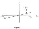
- FIG. 4depicts a current vs. voltage characteristics of the trapped charge memory device with its resistance in a second state
- FIG. 5depicts a composite current vs. voltage characteristics of the trapped charge memory device with both of its resistance states superimposed
- FIG. 6Adepicts a section of a resistive memory material with charge traps
- FIG. 6Bdepicts an energy band diagram of the section of resistive memory material in FIG. 6A;
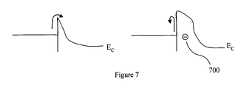
- FIG. 7depicts energy band diagrams of a Schottky barrier without and with a charged trap
- FIG. 8depicts energy band diagrams of trap to trap conduction without and with trapped charge
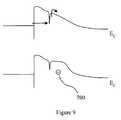
- FIG. 9depicts energy band diagrams of Frenkel-Poole conduction without and with charged trap.
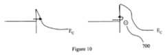
- FIG. 10depicts energy band diagrams of tunneling conduction through a Schottky junction without and with a charged trap.
- arrayrefers to a plurality of objects arranged in a regular pattern.
- CMOrefers to a conductive metal oxide
- conductive linerefers to an interconnect line connecting elements of an integrated circuit (“IC”).
- cross point memory arrayrefers to an array with two sets of generally perpendicular lines with memory cells placed at the intersections between the sets of lines.
- current carrierrefers to charged particles within a conductive or semiconductive material capable of carrying an electrical current, typically a negatively charged electron or a positively charged hole.
- Electroderefers to a low resistivity object through which an electrical current or voltage is brought to another object in contact with the electrode.
- FETrefers to a field effect transistor
- ICrefers to an integrated circuit
- a layerrefers to a coating with a certain thickness.
- a layeris generally located in a plane parallel to the IC substrate.
- Memory Cellrefers to a basic functional structure, usually consisting of a set of devices to store a unit of information, for example one bit.
- Memory Materialrefers to a material that is capable of storing information.
- Memory Plugrefers to various layers of materials arranged between conductive lines and including at least a memory material and typically including a top electrode and a bottom electrode.
- MOCVDrefers to a metalorganic chemical vapor deposition
- PLDrefers to a pulsed laser deposition
- SONOS cellsrefers to a silicon oxide nitride oxide silicon structure—a non-volatile memory technology.
- STOstrontium titanate
- SZOstrontium zirconate
- Thin Filmrefers to a film of thickness generally less than 10 ⁇ m .
- UVrefers to ultra violet
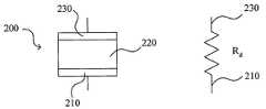
- FIG. 2illustrates a cross-section of a trapped charge memory device according to the present invention.
- the trapped charge memory device 200comprises a bottom electrode 210 , a trapped charge memory body 220 and a top electrode 230 .
- the trapped charge memory devicehas a resistance of R d between the bottom electrode 210 and the top electrode 230 .
- both the top and the bottom electrodesare made of a highly conductive material.
- the trapped charge memory body 220is generally made of a material having the following characteristics: (a) it is a conductive metal oxide; (b) it has a microscopic structure that is single crystalline or poly-crystalline (collectively “crystalline”) or amorphous; (c) it is between 100 ⁇ and 5000 ⁇ in thickness; and (d) it has been modified to have numerous locations of current carrier traps introduced therein.
- a current carriercan be either a negatively charged electron or a positively charged hole.
- the current carrier trap locations, or simply trapsare regions within the trapped charge memory body 220 material causing the presence of localized energy levels within the bandgap of the trapped charge memory body material. These traps are thus capable of trapping, or immobilizing, current carriers within the trapped charge memory body material and affecting its resistance R d .
- the degree of charging or discharging the trapsare dependent upon localized energy levels within the bandgap.
- the carrier occupancycan be affected by an electric field applied across the trapped charge memory body 220 and accompanied by a corresponding current flow. Typically, the electric field will need to be beyond a certain threshold value before it affects carrier occupancy. Consequently, the resistance R d of a properly designed trapped charge memory device 200 can be switched through multiple values following a corresponding number of applied voltage thresholds. The means of creating and configuring these traps will be presently described.
- the trapsmay be located within the crystal lattice. However, for a poly-crystalline trapped charge memory body 220 material, the traps may be located within the grain boundaries or within a molecular structure.
- extrinsic materialscan be introduced into the trapped charge memory body 220 in minute quantities.
- the dopantwould make up less than 10% molecular percentage of the total material.
- some dopantscreate trapping centers at deep energy levels within the bandgap. That is, once captured at these trapping centers, a current carrier would need to acquire a sufficient amount of energy to regain its mobility.
- the elements Cr, Fe or Nican create traps at deep energy levels in STO and in SZO.
- the elements Y, La, Nb and Taprimarily create centers at shallow energy levels which typically do not act as traps.
- Trapscan also be introduced in the trapped charge memory body with high energy radiation or particle beam bombardment.
- UV and X-ray radiationinduces traps in SiO 2 .
- neutron transmutation dopinghas been used to create dopant atoms in silicon.
- Trapscan also be created intrinsically within the trapped charge memory body 220 material during its fabrication. Examples of such mechanisms have been described in U.S. patent application Ser. No. 10/330,512, filed Dec. 26, 2002, already incorporated herein by reference. Furthermore, traps can be created by an electrical initialization process during which oxygen vacancies drift through a complex metal oxide in the presence of an applied electric field. See references “DC Electrical Degradation of Perovskite-Type Titanates (Ceramics, Single Crystal, A Model of the Mechanism): I, II & if,” Rainer Waser et al, J. Am. Ceram. Soc., 73 [6] 1990 PP.
- FIG. 3Adepicts a current vs. voltage characteristics of the trapped charge memory device with its resistance in a first state.
- the I-V line 310are generally ohmic, or linear.
- the values ⁇ VN c1 and +VP c1represent voltage thresholds at which the trapped charge memory body 220 can change the magnitude of the trapped current carriers. However, it should be appreciated that there exists saturation points where either no more or no less current carriers can be trapped. If the trapped charge memory body 220 is in one of these saturation points, then V d can be placed beyond the voltage threshold and still maintain a constant R d .
- either one or both of the top electrode to trapped charge memory body contact and the bottom electrode to trapped charge memory body contactcan be made non-ohmic with the R d exhibiting a corresponding degree of nonlinearity and this is illustrated as I-V curve 320 in FIG. 3B.
- R dWhen the trapped charge memory body 220 is in its first resistive state and a voltage greater than +VP c1 is maintained across the trapped charge memory device for a certain length of time, called the resistance switching time, R d will change to a second state of generally a higher resistance value R 2 , that is the slope of the I-V line 330 in FIG. 4.
- R 2a resistance switching time in the range of from about 0.1 ns to about 100 ⁇ s has been achieved.
- the current Iflows through the trapped charge memory body 220 wherein the traps are not filled with current carriers. However, once a critical electric field strength is exceeded within the trapped charge memory body 220 the traps are subsequently filled with current carriers and the presence of the trapped charge changes the current flow to a generally lower value. This is indicated by Point C with a dashed pointing arrow. Now if V d is taken to a value that is more negative than ⁇ VN c1 for a duration of resistance switching time, then the composite I-V curve 500 switches back from Point D to Point E as indicated by another dashed pointing arrow. Physically, this switching corresponds to a release of charge carriers from the traps.
- the underlying mechanism, when the traps are filled with charges, that causes the change of resistance of the trapped charge memory devicecan be any of the following with, in many cases, analytical modeling expressions available from “Physics of Semiconductor devices,” 2 nd Edition: S. M. Sze, Publisher: John Wiley & Sons, 1981 P. 403, incorporated herein by reference for all purpose, approximating the accompanying J-V characteristics:
- FIG. 6Adepicts a section of a resistive memory material 600 with charge traps 610 .
- Each charge trap 610is shown carrying an amount of negative charge.
- the charge traps 610act to reduce the flow of electrons by repelling those electrons traveling nearby.
- the same charge traps 610can enhance the flow of holes by attracting those holes traveling nearby.
- a trapped chargecould either enhance or deplete the concentration of free current carriers in its vicinity.
- FIG. 6Bshows a localized elevation 620 of both conduction band E c and valence band E v .
- the presence of the trapped chargeraises or lowers, depending upon the charge type, the height of the Schottky barrier at the top electrode to trapped charge memory body contact or at the bottom electrode to trapped charge memory body contact.
- the trapped chargewould raise the Schottky barrier for free carriers of like charge polarity by introducing an opposition electric field at the contact.
- the trapped chargewould lower the Schottky barrier for free carriers of the opposite polarity by introducing an enhancement electric field at the contact. Consequently, a higher Schottky barrier acts to increase the resistance of the trapped charge memory device and vice versa.
- the corresponding energy band diagrams of the Schottky barrierare shown in FIG. 7 wherein the left side has no charged trap but the right side has a charged trap 700 and the free carriers are electrons.
- the interface between a metal electrode and a CMO filmcan have a depletion region, like in a Schottky barrier, and traps at the interface can affect conduction.
- the mechanism of trap to trap hopping, or “hopping conduction”was presented in “New conduction and reversible memory phenomena in thin insulating films” by J. G. Simmons and R. R. Verderber, Proc. Roy. Soc. A. 301, 1967 PP. 77-102. al 1967, already incorporated herein by reference.
- Trap to trap hopping, while allowing bipolar conductionis affected by the presence of trapped charge and are illustrated in the energy band diagrams without (left hand) and with trapped charge (right hand) of FIG. 8.
- Frenkel-Poole conductionis an electric field assisted thermionic emission from moderately deep traps.
- charges trapped in other energy levelswhile not participating in the emission of current carriers, could affect the resistance as well.
- the traps that participate in the Frenkel-Poole conductionand the charged traps responsible for the resistance memory effect.
- the associated trapped chargeswill affect the resistance by modifying the barrier height in a way similar to mechanism 2 above.
- the corresponding energy band diagrams of Frenkel-Poole Conduction without (top) and with charged trap (bottom)are illustrated in FIG. 9.
- Tunneling conductionalso see above reference by S. M. Sze 1981, can happen in which current carriers tunnel from the electrode directly to the conduction band (for electrons) or valence band (for holes) in a Schottky-like structure.
- the trapped charge in the depletion regioncan affect the resistance in a way similar to mechanism 2 above.
- the corresponding energy band diagrams of tunneling conduction through a Schottky junction without (left hand) and with a charged trap (right hand)are illustrated in FIG. 10.
- the trapscan be charged and discharged in a variety of ways. For example, under a high electric field the current carriers can tunnel from an electrode to the traps or between neighboring traps. For another example, the traps can also be charged by trapping free current carriers with lower energy. Clearly, the concentration of the traps, be it by molecular counts, by weight or by volume, will also determine their net total effect on the resistance R d of the trapped charge memory device. It should also become clear by now that, with the multitude of the above mechanisms 1 - 6 each capable of changing the resistance R d of the trapped charge memory device.
- the trapped charge memory devicecan be designed and made to exhibit M distinct voltage switchable pre-determined levels of resistance values R 1 , R 2 , . .
- R Msuch that R j switches to R j+l when V d goes above +VP cj and R j+i switches back to R j when V d drops below ⁇ VN cj .
- longer voltage pulsescan be used instead or in conjunction with higher voltage pulses to reach the desired resistance value.
- the trapped charge memory devicecan function as a simple, generic circuit component capable of easy integration into a variety of electronic systems including the adjustment of precision analog circuits, programmable logic, fuses for selection of redundant areas, over-voltage history detector and dynamically programmable-gain amplifier, etc.
- A*effective Richardson constant
- ⁇ Bbarrier height
- ⁇ iinsulator dynamic permittivity
- m*effective mass
- dinsulator thickness
- ⁇ E aeactivation energy of electrons
- hreduced Planck constant
- ⁇ E aiactivation energy of ions
- Jcurrent density
- Vterminal voltage.
- Positive constants independent of V or Tare b, c, and d′.
- materials parametersmaterial for each of top electrode, trapped charge memory body and bottom electrode; material, concentration and energy levels of current carrier traps within the trapped charge memory body;
- electrical parametersbody resistivity of the trapped charge memory body, degree of carrier occupancy for each type of carrier trap, barrier height and depth at the top electrode-to-trapped charge memory body contact and at the bottom electrode-to-trapped charge memory body contact;
- geometric parameterscross sectional dimensions and thickness for each of top electrode, trapped charge memory body and bottom electrode.
- the fabrication of the trapped charge memory device as describedbeing basically a multi-layered thin film structure with each film typically of a thickness less than 10 ⁇ m, includes (1) providing a substrate on which to first form the bottom electrode 210 material, (2) forming or depositing the trapped charge memory body 220 material having current carrier traps, with a variety of means to be presently described, that may or may not already have the finally desired degree of carrier occupancy, on top of the bottom electrode 210 , (3) forming or depositing the top electrode 230 material on top of the trapped charge memory body 220 and, under conditions where the current carrier traps of the formed trapped charge memory body do not yet have the finally desired degree of carrier occupancy, (4) conditioning the trapped charge memory device with a variety of means, to be presently described, to impart the current carrier traps with the finally desired degree of carrier occupancy.
- conditioning of the trapped charge memory bodycan also take place during the fabrication process, e.g., just before step (3).
- the benefit of conditioningis that typically it is desirable to have all the individual trapped charge memory device within a memory system at a uniform state of carrier occupancy at the end of the fabrication process. This allows for quicker and therefore cheaper testing of the memory system. For example, it is desirable to have all the trapped charge memory device either at a high resistance state or at a low resistance state as opposed to being at some intermediate state of carrier occupancy.
- Some specific fabrication processes for the trapped charge memory deviceinclude: Solution based spin on followed by high temperature anneal, pulsed laser deposition (PLD), sputtering, and metalorganic chemical vapor deposition (MOCVD).
- PLDpulsed laser deposition
- MOCVDmetalorganic chemical vapor deposition
- the substrate materialshould be polycrystalline or single crystalline, be conductive, and can itself serve as an electrode already.
- the material for the trapped charge memory bodyis generally conductive metal oxides (CMO) with some of these CMO generally having a crystalline or polycrystalline perovskite structure.
- CMO materialincludes two or more metals, the metals being selected from the group consisting of transition metals, alkaline earth metals and rare earth metals.
- the specific compositioncan, however, be any of a number of varieties, including the following examples of manganites: PCMO Pr .7 Ca .3 MnO 3 LCMO La .7 Ca .3 MnO 3 LSMO La .7 Sr .3 MnO 3 ,
- Titanatese.g., STO:Cr, STO:Fe, STO:Ni
- zirconatese.g., SZO:Cr, Ca 2 Nb 2 O 7 :Cr, and Ta 2 O 5 :Cr
- high Tc superconductorse.g., YBCO
- the trapped charge memory body material employed in this inventionis not limited to either the conductive metal oxide or the perovskite crystal lattice structure. Any material approximating the I-V characteristics as described above may be suitable for use as the trapped charge memory body material of this invention. Additionally, the chemical and materials properties of the trapped charge memory body material are selected to meet various target electrical specifications.
- the trapped charge memory body materialpreferably has a resistivity of not greater than about 1 Ohm-cm, exhibits a switchable resistance change of at least about 10X, and has this resistance change triggered by the application of a voltage pulse of not longer than about 100 ns duration and not greater than about 3 Volt in magnitude.
- the trapped charge memory body material thicknessis dictated by the desired resistive states of the trapped charge memory body material and the write threshold voltage.
- a trapped charge memory body material with a write threshold voltage of 1.5 voltsmight be between 1000 ⁇ and 3000 ⁇ in thickness.
- the material selection for the electrode layerswould ideally be as thin as possible while still preventing metal inter-diffusion and, if necessary, being useful as a seed layer.
- Typical electrode material commonly used in fabricationincludes Pt, Au, Ag and Al. While the electrode layers would only be used as a barrier to prevent metal inter-diffusion, then a thin layer of metal, e.g. TiN, could be used. Any number of electrically conductive materials can be used for a seed layer of the CMO material.
- the seed layercould be a conductive perovskite, such as LaNiO 3 or SrRuO 3 on Pt, a conductive metal oxide, such as IrO 2 on Ir or RuO 2 on Ru, a noble metal such as Pt on TiN.
- the top and bottom electrode layerscould use the same conductive layer for the seed layer.
- STO or SZOcan be doped by adding an element that has a different preferred oxidation state (a different charge when ionized) when it replaces an element within the crystal matrix.
- chromium (Cr)with a +3 oxidation state, can replace zirconium (Zr) with a +4 oxidation state.
- free carrierscan either compensate for the charge imbalance by creation of appropriate vacancies (e.g., oxygen vacancies) or by change of the valence on a matrix element.
- a dopant atomusually substitutes for a matrix element based, at least partly, on the similarity of ionic radii.
- lanthanum (La)primarily substitutes for strontium (Sr)
- Crprimarily substitutes for Zr in SZO.
- cation vacanciesare rare (i.e., there are few Sr and Zr vacancies) but anion vacancies (i.e., oxygen) are common. Therefore, adding Cr to SZO generates both oxygen vacancies and free holes.
- oxygen vacanciesone vacancy for every 2 Cr atoms
- free electronsprimarily compensate for La in SZO. Therefore adding La drastically lowers the resistance of SZO.
- tantalum (Ta) or niobium (Nb)can substitute for Zr to lower SZO resistivity.
- vacanciescan also act to create charge traps.
- the charge imbalance caused by a vacancycan be compensated for by the same mechanisms that compensate for the intentional addition of a dopant.
- an oxygen vacancycompensated for by two Cr atoms, provides no free carriers but if there is insufficient Cr atoms for full compensation, these oxygen vacancies lead to free electrons.
- Some dopantscreate centers at deep levels within the bandgap. Such dopants create centers where a trapped charge would need a high level of energy to exit that level, effectively creating traps with the deep levels.
- Cr, Fe or Nican create traps in STO and SZO.
- yttrium (Y), La, Nb and Tacould only create centers at shallow levels which would not act as traps. Traps can also be introduced into the trapped charge memory body with high energy radiation or particle beam bombardment, for example UV and X-ray in SiO 2 . Also neutron transmutation doping has been used to create dopant atoms in silicon. UV light can be used, as with EPROM memories, to discharge all traps, therefore bringing the memory devices to similar Rd levels. Alternatively, all memory devices can be subjected, globally or sequentially, to an electric pulse, whether by passing an electric current or subjecting the memory devices to an electric field. This electrical operation will affect the charges stored in the traps and result in a more uniform charge level in all the traps.
- the diodescan be (i) a PN junction diode made of amorphous, microcrystalline, polycrystalline or single crystal semiconductor (e.g.
- a metal-semiconductor Schottky diode(iii) a junction field-effect transistor with gate connected to source (or to drain); (iv) a MOSFET with gate either floating, or connected to source or connected to drain; (v) a Zener diode, avalanche diode, or tunnel diode; (vi) a four-layer diode (SCR); (vii) a P-I-N diode made of amorphous, microcrystalline, polycrystalline or single crystal semiconductor.
- MIMmetal-insulator-metal
- a 2-terminal trapped charge memory device with voltage switchable multi-level resistance R dis disclosed that is based upon a wide variety of material, fabrication and design parameters affecting the electrical terminal behavior of the trapped charge memory device.
- the inventionhas been described using exemplary preferred embodiments. However, for those skilled in this field, the preferred embodiments can be easily adapted and modified to suit additional applications without departing from the spirit and scope of this invention. Thus, it is to be understood that the scope of the invention is not limited to the disclosed embodiments. On the contrary, it is intended to cover various modifications and similar arrangements based upon the same operating principle. The scope of the claims, therefore, should be accorded the broadest interpretations so as to encompass all such modifications and similar arrangements.
Landscapes
- Engineering & Computer Science (AREA)
- Chemical & Material Sciences (AREA)
- Materials Engineering (AREA)
- Computer Hardware Design (AREA)
- Crystallography & Structural Chemistry (AREA)
- Manufacturing & Machinery (AREA)
- Semiconductor Memories (AREA)
Abstract
Description
- This application is a continuation-in-part of U.S. patent application Ser. No. 10/249,846, filed May 12, 2003, which claims the benefit of U.S. Provisional Application No. 60/400,849, filed Aug. 02, 2002, and U.S. Provisional Application No. 60/422,922, filed Oct. 31, 2002, all of which are incorporated herein by reference in their entireties and for all purposes. This application is related to the following U.S. patent applications: application Ser. No. 10/360,005, filed Feb. 7, 2003; application Ser. No. 10/330,512, filed Dec. 26, 2002; application Ser. No. 10/330,153, filed Dec. 26, 2002; application Ser. No. 10/330,964, filed Dec. 26, 2002; application Ser. No. 10/330,170, filed Dec. 26, 2002; application Ser. No. 10/330,900, filed Dec. 26, 2002; application Ser. No. 10/330,150, filed Dec. 26, 2002; application Ser. No. 10/330,965, filed Dec. 26, 2002; application Ser. No. 10/249,848, filed May 12, 2003; application Ser. No. 10/612,733, filed Jul. 1, 2003; application Ser. No. 10/613,099, filed Jul. 1, 2003; application Ser. No. 10/612,191, filed Jul. 1, 2003; application Ser. No. 10/612,263, filed Jul. 1, 2003; and application Ser. No. 10/612,776, filed Jul. 1, 2003. All of the above applications are hereby incorporated herein by reference in their entireties and for all purposes.[0001]
- This invention concerns the general field of memory devices. Specifically, the present invention is directed to two terminal memory devices.[0002]
- The use of stored or trapped charges is the dominant mechanism for storing data in a non-volatile memory cell. The charges of the memory cell are trapped or stored at various internal structures, such as: (a) floating gates; (b) material interfaces between, for example, a nitride and an oxide (SONOS cells); and (c) regions within an insulator that contain islands of conductive materials such as silicon rich oxides.[0003]
- During device operation, these trapped charges function to modify, for example, the silicon surface conductivity of a FET. A corresponding general device configuration is illustrated in FIG. 1. A FET[0004]100 includes a
source 130 and adrain 120 separated by acontrol gate 110. This FET100 can be of n-type or p-type. For simplicity we will describe an n-type FET. Thus, thedrain 120 and thesource 130 are both made of an n-doped semiconductor material while thesubstrate 140 is made of a p-doped semiconductor material. When a positive voltage is applied to thecontrol gate 110, electrons within thesubstrate 140 are attracted toward thecontrol gate 110 and form aninversion layer 150 in an area called the ‘channel’ that is within thesubstrate 140 and under thecontrol gate 110. The channel then allows current conduction between thedrain 120 and thesource 130. - Notwithstanding the foregoing description, the presence of any trapped[0005]
charges 160 within theoxide 170 and between thecontrol gate 110 and thesubstrate 140 will modify the required value of the voltage applied to thecontrol gate 110 to create theinversion layer 150. For a case of negative trappedcharges 160, the higher the magnitude of trapped charge the higher the required voltage would have to be. The reason is that the negative charges trapped in the oxide will repel the electrons away from the channel, necessitating the application of a higher positive voltage on thecontrol gate 110 to counteract this effect. - For each of the above devices, the magnitude of trapped charges can be altered through various mechanisms. Retrieving data can then be accomplished by sensing the voltage that is required to create the inversion layer.[0006]
- The present invention discloses a 2-terminal trapped charge memory device with a voltage switchable multi-level resistance R[0007]d. In addition to a top electrode and a bottom electrode, the trapped charge memory device includes a trapped charge memory body sandwiched between the top electrode and the bottom electrode. The trapped charge memory body includes current carrier traps with at least one of whose energy levels, respective degrees of carrier occupancy and concentration determine the Rd. The respective degrees of carrier occupancy of the current carrier traps are modifiable by the height and width of an applied write voltage pulse resulting in a desired switching behavior of the multi-level resistance Rd. The mechanism of modification of carrier occupancy can be any of carrier tunneling, free carrier capturing, trap-hopping conduction and Frenkel-Poole conduction. The range of achievable resistance switching time can be made from about 0.1 ns to about 100 μs. Additionally, one or both of the top electrode-to-memory body contact and the bottom electrode-to-memory body contact can be made non-ohmic to create a corresponding nonlinearity of Rd.
- A variety of material, fabrication and design parameters are identified affecting the electrical terminal behavior of the 2-terminal trapped charge memory device. The trapped charge memory body can be made of an insulator, a conductor, a conductive oxide, a polymer, organic molecules, carbon nanotubes or a semiconductor with a layer thickness between about 100 Å and about 5000 Å. The trapped charge memory body structure can be single-crystalline, poly-crystalline or amorphous. The current carrier traps and their degree of occupancy can be created with the addition of dopant varieties or with an initialization procedure during or after the fabrication of the memory device. The initialization procedure can be high energy radiation or particle beam bombardment.[0008]
- The current invention will be better understood and the summary of the invention set forth above will become apparent when consideration is given to the following detailed description of the preferred embodiments. For clarity of explanation, the detailed description further makes reference to the attached drawings herein:[0009]
- FIG. 1 depicts a cross-section of a prior art memory device;[0010]
- FIG. 2 depicts a cross-section and a schematic diagram of the trapped charge memory device according to the present invention;[0011]
- FIG. 3A depicts a current vs. voltage characteristics of the trapped charge memory device with its resistance in a first state;[0012]
- FIG. 3B depicts another current vs. voltage characteristics of the trapped charge memory device with its resistance still in a first state while exhibiting a degree of nonlinearity;[0013]
- FIG. 4 depicts a current vs. voltage characteristics of the trapped charge memory device with its resistance in a second state;[0014]
- FIG. 5 depicts a composite current vs. voltage characteristics of the trapped charge memory device with both of its resistance states superimposed;[0015]
- FIG. 6A depicts a section of a resistive memory material with charge traps;[0016]
- FIG. 6B depicts an energy band diagram of the section of resistive memory material in FIG. 6A;[0017]
- FIG. 7 depicts energy band diagrams of a Schottky barrier without and with a charged trap;[0018]
- FIG. 8 depicts energy band diagrams of trap to trap conduction without and with trapped charge;[0019]
- FIG. 9 depicts energy band diagrams of Frenkel-Poole conduction without and with charged trap; and[0020]
- FIG. 10 depicts energy band diagrams of tunneling conduction through a Schottky junction without and with a charged trap.[0021]
- As used in the present specification, the following words and phrases are generally intended to have the meanings as set forth below, except to the extent that the context in which they are used indicates otherwise. The following abbreviations and terms have the indicated meanings throughout:[0022]
- The term “array” refers to a plurality of objects arranged in a regular pattern.[0023]
- The term “CMO” refers to a conductive metal oxide.[0024]
- The term “conductive line” refers to an interconnect line connecting elements of an integrated circuit (“IC”).[0025]
- The term “cross point memory array” refers to an array with two sets of generally perpendicular lines with memory cells placed at the intersections between the sets of lines.[0026]
- The term “current carrier” refers to charged particles within a conductive or semiconductive material capable of carrying an electrical current, typically a negatively charged electron or a positively charged hole.[0027]
- The term “electrode” refers to a low resistivity object through which an electrical current or voltage is brought to another object in contact with the electrode.[0028]
- The term “FET” refers to a field effect transistor.[0029]
- The term “IC” refers to an integrated circuit.[0030]
- The term “layer” refers to a coating with a certain thickness. Within an IC, a layer is generally located in a plane parallel to the IC substrate.[0031]
- The term “Memory Cell” refers to a basic functional structure, usually consisting of a set of devices to store a unit of information, for example one bit.[0032]
- The term “Memory Material” refers to a material that is capable of storing information.[0033]
- The term “Memory Plug” refers to various layers of materials arranged between conductive lines and including at least a memory material and typically including a top electrode and a bottom electrode.[0034]
- The term “MOCVD” refers to a metalorganic chemical vapor deposition.[0035]
- The term “PLD” refers to a pulsed laser deposition.[0036]
- The term “SONOS cells” refers to a silicon oxide nitride oxide silicon structure—a non-volatile memory technology.[0037]
- The term “STO” refers to strontium titanate.[0038]
- The term “SZO” refers to strontium zirconate.[0039]
- The term “Thin Film” refers to a film of thickness generally less than 10 μm .[0040]
- The term “UV” refers to ultra violet.[0041]
- In the following description, numerous specific details are set forth in order to provide a thorough understanding of the present invention. However, it will become obvious to those skilled in the art that the present invention may be practiced without these specific details. In other instances, well-known methods, procedures, materials, components and circuitry have not been described in detail to avoid unnecessary obscuring aspects of the present invention. The detailed description is presented largely in terms of simplified semiconductor device cross sections, bulk and interface energy band diagrams and associated electrical terminal I-V characteristics. These descriptions and representations are the means used by those experienced or skilled in the art to concisely and most effectively convey the substance of their work to others skilled in the art.[0042]
- FIG. 2 illustrates a cross-section of a trapped charge memory device according to the present invention. The trapped[0043]
charge memory device 200 comprises abottom electrode 210, a trappedcharge memory body 220 and atop electrode 230. The trapped charge memory device has a resistance of Rdbetween thebottom electrode 210 and thetop electrode 230. Generally, both the top and the bottom electrodes are made of a highly conductive material. The trappedcharge memory body 220 is generally made of a material having the following characteristics: (a) it is a conductive metal oxide; (b) it has a microscopic structure that is single crystalline or poly-crystalline (collectively “crystalline”) or amorphous; (c) it is between 100 Å and 5000 Å in thickness; and (d) it has been modified to have numerous locations of current carrier traps introduced therein. - In the above, a current carrier can be either a negatively charged electron or a positively charged hole. The current carrier trap locations, or simply traps, are regions within the trapped[0044]
charge memory body 220 material causing the presence of localized energy levels within the bandgap of the trapped charge memory body material. These traps are thus capable of trapping, or immobilizing, current carriers within the trapped charge memory body material and affecting its resistance Rd. - Furthermore, the degree of charging or discharging the traps are dependent upon localized energy levels within the bandgap. Also, the carrier occupancy can be affected by an electric field applied across the trapped[0045]
charge memory body 220 and accompanied by a corresponding current flow. Typically, the electric field will need to be beyond a certain threshold value before it affects carrier occupancy. Consequently, the resistance Rdof a properly designed trappedcharge memory device 200 can be switched through multiple values following a corresponding number of applied voltage thresholds. The means of creating and configuring these traps will be presently described. - For a crystalline trapped[0046]
charge memory body 220 material, the traps may be located within the crystal lattice. However, for a poly-crystalline trappedcharge memory body 220 material, the traps may be located within the grain boundaries or within a molecular structure. - To foster the creation of traps, extrinsic materials, called dopants, can be introduced into the trapped[0047]
charge memory body 220 in minute quantities. Typically, the dopant would make up less than 10% molecular percentage of the total material. As a result, some dopants create trapping centers at deep energy levels within the bandgap. That is, once captured at these trapping centers, a current carrier would need to acquire a sufficient amount of energy to regain its mobility. For example, the elements Cr, Fe or Ni can create traps at deep energy levels in STO and in SZO. On the other hand, the elements Y, La, Nb and Ta primarily create centers at shallow energy levels which typically do not act as traps. See the technical papers “Photochromism in Ni-doped SrTiO3,” P. Koidl et al, Physical review B, Vol. 14, No. 7, Oct. 7, 1976 PP. 2703-2708, and “Photoinduced Phenomina in Sr1−xCaxTiO2, 0<=×<=0,12,” S. A. Basun et al, Ferroelectrics, 1996, Vol. 183, PP. 255-264, both incorporated herein by reference and for all purposes. - Traps can also be introduced in the trapped charge memory body with high energy radiation or particle beam bombardment. For example, UV and X-ray radiation induces traps in SiO[0048]2. Also, neutron transmutation doping has been used to create dopant atoms in silicon.
- Traps can also be created intrinsically within the trapped[0049]
charge memory body 220 material during its fabrication. Examples of such mechanisms have been described in U.S. patent application Ser. No. 10/330,512, filed Dec. 26, 2002, already incorporated herein by reference. Furthermore, traps can be created by an electrical initialization process during which oxygen vacancies drift through a complex metal oxide in the presence of an applied electric field. See references “DC Electrical Degradation of Perovskite-Type Titanates (Ceramics, Single Crystal, A Model of the Mechanism): I, II & if,” Rainer Waser et al, J. Am. Ceram. Soc., 73 [6] 1990 PP. 1645-1663 and “New conduction and reversible memory phenomena in thin insulating films” J. G. Simmons and R. R. Verderber, Proc. Roy. Soc. A. 301, 1967 PP. 77-102, both incorporated herein by reference and for all purposes. - An example of a trapped charge memory device whose resistance R[0050]dcan be switched through two distinct values is illustrated in FIG. 3A, FIG. 3B and FIG. 4. FIG. 3A depicts a current vs. voltage characteristics of the trapped charge memory device with its resistance in a first state. When a voltage Vdis applied across the trapped
charge memory device 200, a current flow I occurs. As long as the voltage Vdstays within the following critical values: - −VNc1<=Vd<=+VPc1 (1)
- the[0051]
I-V line 310 are generally ohmic, or linear. The values −VNc1and +VPc1represent voltage thresholds at which the trappedcharge memory body 220 can change the magnitude of the trapped current carriers. However, it should be appreciated that there exists saturation points where either no more or no less current carriers can be trapped. If the trappedcharge memory body 220 is in one of these saturation points, then Vdcan be placed beyond the voltage threshold and still maintain a constant Rd. In FIG. 3A, the slope of theI-V line 310 defines a first resistance value of R1such that Rd=R1. - For certain applications, either one or both of the top electrode to trapped charge memory body contact and the bottom electrode to trapped charge memory body contact can be made non-ohmic with the R[0052]dexhibiting a corresponding degree of nonlinearity and this is illustrated as
I-V curve 320 in FIG. 3B. - When the trapped[0053]
charge memory body 220 is in its first resistive state and a voltage greater than +VPc1is maintained across the trapped charge memory device for a certain length of time, called the resistance switching time, Rdwill change to a second state of generally a higher resistance value R2, that is the slope of theI-V line 330 in FIG. 4. In practice, a resistance switching time in the range of from about 0.1 ns to about 100 μs has been achieved. - FIG. 5 depicts a composite[0054]
I-V curve 500 of the trapped charge memory device with both of its resistance states superimposed. Starting with Point A of Vd=0 thus I=0, within the region between Point A and Point B and characterized by: - 0<=Vd<=+VPc1 (2)
- the current I flows through the trapped[0055]
charge memory body 220 wherein the traps are not filled with current carriers. However, once a critical electric field strength is exceeded within the trappedcharge memory body 220 the traps are subsequently filled with current carriers and the presence of the trapped charge changes the current flow to a generally lower value. This is indicated by Point C with a dashed pointing arrow. Now if Vdis taken to a value that is more negative than −VNc1for a duration of resistance switching time, then thecomposite I-V curve 500 switches back from Point D to Point E as indicated by another dashed pointing arrow. Physically, this switching corresponds to a release of charge carriers from the traps. - The underlying mechanism, when the traps are filled with charges, that causes the change of resistance of the trapped charge memory device can be any of the following with, in many cases, analytical modeling expressions available from “Physics of Semiconductor devices,” 2[0056]ndEdition: S. M. Sze, Publisher: John Wiley & Sons, 1981 P. 403, incorporated herein by reference for all purpose, approximating the accompanying J-V characteristics:
- The presence of the trapped charge modifies or otherwise alters the conductivity of the bulk trapped charge memory body material. An example is illustrated in FIG. 6A which depicts a section of a[0057]
resistive memory material 600 with charge traps610. Eachcharge trap 610 is shown carrying an amount of negative charge. Here, the charge traps610 act to reduce the flow of electrons by repelling those electrons traveling nearby. On the other hand, the same charge traps610 can enhance the flow of holes by attracting those holes traveling nearby. Thus, depending upon its polarity, a trapped charge could either enhance or deplete the concentration of free current carriers in its vicinity. The corresponding energy band diagram is illustrated in FIG. 6B showing alocalized elevation 620 of both conduction band Ecand valence band Ev. - The presence of the trapped charge raises or lowers, depending upon the charge type, the height of the Schottky barrier at the top electrode to trapped charge memory body contact or at the bottom electrode to trapped charge memory body contact. The trapped charge would raise the Schottky barrier for free carriers of like charge polarity by introducing an opposition electric field at the contact. On the other hand, the trapped charge would lower the Schottky barrier for free carriers of the opposite polarity by introducing an enhancement electric field at the contact. Consequently, a higher Schottky barrier acts to increase the resistance of the trapped charge memory device and vice versa. The corresponding energy band diagrams of the Schottky barrier are shown in FIG. 7 wherein the left side has no charged trap but the right side has a charged[0058]
trap 700 and the free carriers are electrons. - The interface between a metal electrode and a CMO film can have a depletion region, like in a Schottky barrier, and traps at the interface can affect conduction. The mechanism of trap to trap hopping, or “hopping conduction” was presented in “New conduction and reversible memory phenomena in thin insulating films” by J. G. Simmons and R. R. Verderber, Proc. Roy. Soc. A. 301, 1967 PP. 77-102. al 1967, already incorporated herein by reference. Trap to trap hopping, while allowing bipolar conduction, is affected by the presence of trapped charge and are illustrated in the energy band diagrams without (left hand) and with trapped charge (right hand) of FIG. 8.[0059]
- Frenkel-Poole conduction, also see above reference by S. M. Sze 1981, is an electric field assisted thermionic emission from moderately deep traps. Here, charges trapped in other energy levels, while not participating in the emission of current carriers, could affect the resistance as well. Under this mechanism there are two types of traps, the traps that participate in the Frenkel-Poole conduction and the charged traps responsible for the resistance memory effect. The associated trapped charges will affect the resistance by modifying the barrier height in a way similar to mechanism[0060]2 above. The corresponding energy band diagrams of Frenkel-Poole Conduction without (top) and with charged trap (bottom) are illustrated in FIG. 9.
- Tunneling conduction, also see above reference by S. M. Sze 1981, can happen in which current carriers tunnel from the electrode directly to the conduction band (for electrons) or valence band (for holes) in a Schottky-like structure. Here, the trapped charge in the depletion region can affect the resistance in a way similar to mechanism[0061]2 above. The corresponding energy band diagrams of tunneling conduction through a Schottky junction without (left hand) and with a charged trap (right hand) are illustrated in FIG. 10.
- Orbital ordering, see the technical papers “Lattice effects in magnetoresistive manganese perovskites,” A. J. Millis, NATURE, Vol. 392, Mar. 12, 1998, PP. 147-150 and “X-ray resonant scattering studies of orbital and charge ordering in Pr[0062]1−xCaxMnO3” M. v. Zimmermann et al, Physical Review B, Vol. 64, 195133, 2001, PP. 1-17 both incorporated herein by reference and for all purposes, is a mechanism in which the electron orbitals in a crystal lattice have a preferred direction, typically in an ordered pattern, such that the resistivity of the crystal lattice will be higher than the case wherein the ordered pattern is disrupted by the addition of charged traps.
- For those skilled in the art, while the charges and energy band diagrams from FIG. 6A through FIG. 10 are largely illustrated for electron conduction near the conduction band E[0063]c, it should be understood by now that the same mechanisms1-6 above are equally applicable to hole conduction near the valence band Evas well.
- By now it should be clear that the traps can be charged and discharged in a variety of ways. For example, under a high electric field the current carriers can tunnel from an electrode to the traps or between neighboring traps. For another example, the traps can also be charged by trapping free current carriers with lower energy. Clearly, the concentration of the traps, be it by molecular counts, by weight or by volume, will also determine their net total effect on the resistance R[0064]dof the trapped charge memory device. It should also become clear by now that, with the multitude of the above mechanisms1-6 each capable of changing the resistance Rdof the trapped charge memory device. The trapped charge memory device can be designed and made to exhibit M distinct voltage switchable pre-determined levels of resistance values R1, R2, . . . , RMsuch that Rjswitches to Rj+lwhen Vdgoes above +VPcjand Rj+iswitches back to Rjwhen Vddrops below −VNcj. Alternatively, longer voltage pulses can be used instead or in conjunction with higher voltage pulses to reach the desired resistance value.
- In addition to functioning as a memory material in an electronic memory system, the trapped charge memory device can function as a simple, generic circuit component capable of easy integration into a variety of electronic systems including the adjustment of precision analog circuits, programmable logic, fuses for selection of redundant areas, over-voltage history detector and dynamically programmable-gain amplifier, etc.[0065]
- For those skilled in the art, it should become clear by now that, to find a set of specific and quantitative materials, electrical and geometric device parameters for the trapped charge memory device so that it does exhibit the above pre-determined levels of resistance values R[0066]1, R2, . . . , RMswitchable at the various pre-determined voltage magnitudes VPcjand VNcjit takes the combination of analytical modeling expressions and a number of systematic, parametric experiments directed at an initial approximate ranging followed by converging these materials, electrical and geometric device parameters into their respective final values. The following, while not being a complete set, lists some analytical modeling expressions from above reference by S. M. Sze 1981:
- with a voltage and temperature[0068]
- dependence of ˜T2exp(+α{square root}{square root over (V)}/T−qφB/kT) (3A)
- with a voltage and temperature[0070]
- dependence of ˜V exp(+2α{square root}{square root over (V)}/T−qφB/kT) (3B)
- with a voltage and temperature[0072]
- dependence of ˜V2exp(−b/V) (3C)
- Ohmic conduction:[0073]
- J˜ξ exp(−ΔEae/kT)
- with a voltage and temperature[0074]
- dependence of ˜V exp(−c/T) (3D)
- Ionic conduction:[0075]
- J ˜ξ/T) exp(−ΔEai/kT)
- with a voltage and temperature[0077]
- dependence of (3E)
- Where:[0078]
- A*=effective Richardson constant, φ[0079]B=barrier height, ξ32 electric field, εi=insulator dynamic permittivity, m*=effective mass, d=insulator thickness, ΔEae=activation energy of electrons, h=reduced Planck constant, ΔEai=activation energy of ions, and a ≡ {square root}{square root over (q/(4πεid))}. V=ξd, J=current density, V=terminal voltage. Positive constants independent of V or T are b, c, and d′.
- The following enumerates some specific, although not exhaustive, examples of device parameters of the trapped charge memory device:[0080]
- materials parameters—material for each of top electrode, trapped charge memory body and bottom electrode; material, concentration and energy levels of current carrier traps within the trapped charge memory body;[0081]
- electrical parameters—body resistivity of the trapped charge memory body, degree of carrier occupancy for each type of carrier trap, barrier height and depth at the top electrode-to-trapped charge memory body contact and at the bottom electrode-to-trapped charge memory body contact; and[0082]
- geometric parameters—cross sectional dimensions and thickness for each of top electrode, trapped charge memory body and bottom electrode.[0083]
- The fabrication of the trapped charge memory device as described, being basically a multi-layered thin film structure with each film typically of a thickness less than 10 μm, includes (1) providing a substrate on which to first form the[0084]
bottom electrode 210 material, (2) forming or depositing the trappedcharge memory body 220 material having current carrier traps, with a variety of means to be presently described, that may or may not already have the finally desired degree of carrier occupancy, on top of thebottom electrode 210, (3) forming or depositing thetop electrode 230 material on top of the trappedcharge memory body 220 and, under conditions where the current carrier traps of the formed trapped charge memory body do not yet have the finally desired degree of carrier occupancy, (4) conditioning the trapped charge memory device with a variety of means, to be presently described, to impart the current carrier traps with the finally desired degree of carrier occupancy. Alternatively, conditioning of the trapped charge memory body can also take place during the fabrication process, e.g., just before step (3). The benefit of conditioning is that typically it is desirable to have all the individual trapped charge memory device within a memory system at a uniform state of carrier occupancy at the end of the fabrication process. This allows for quicker and therefore cheaper testing of the memory system. For example, it is desirable to have all the trapped charge memory device either at a high resistance state or at a low resistance state as opposed to being at some intermediate state of carrier occupancy. - Some specific fabrication processes for the trapped charge memory device include: Solution based spin on followed by high temperature anneal, pulsed laser deposition (PLD), sputtering, and metalorganic chemical vapor deposition (MOCVD).[0085]
- The substrate material should be polycrystalline or single crystalline, be conductive, and can itself serve as an electrode already.[0086]
- The material for the trapped charge memory body is generally conductive metal oxides (CMO) with some of these CMO generally having a crystalline or polycrystalline perovskite structure. Generally, the CMO material includes two or more metals, the metals being selected from the group consisting of transition metals, alkaline earth metals and rare earth metals.[0087]
- The specific composition can, however, be any of a number of varieties, including the following examples of manganites:[0088]
PCMO Pr.7Ca.3MnO3 LCMO La.7Ca.3MnO3 LSMO La.7Sr.3MnO3, - Titanates (e.g., STO:Cr, STO:Fe, STO:Ni), zirconates (e.g., SZO:Cr, Ca[0089]2Nb2O7:Cr, and Ta2O5:Cr) and high Tc superconductors (e.g., YBCO). Notice that the elements Cr, Fe or Ni can create traps at deep energy levels in STO and in SZO. In this case, the traps are created intrinsically within the trapped charge memory body material during its fabrication. It is remarked that, MnO3, when combined with the rare earth metals La, Pr or some combination thereof and the alkaline earth metals Ca, Sr or some combination thereof, has been found to produce a particularly effective CMO material. Notice that the trapped charge memory body material employed in this invention is not limited to either the conductive metal oxide or the perovskite crystal lattice structure. Any material approximating the I-V characteristics as described above may be suitable for use as the trapped charge memory body material of this invention. Additionally, the chemical and materials properties of the trapped charge memory body material are selected to meet various target electrical specifications. For one example, the trapped charge memory body material preferably has a resistivity of not greater than about 1 Ohm-cm, exhibits a switchable resistance change of at least about 10X, and has this resistance change triggered by the application of a voltage pulse of not longer than about 100 ns duration and not greater than about 3 Volt in magnitude. For another example, the trapped charge memory body material thickness is dictated by the desired resistive states of the trapped charge memory body material and the write threshold voltage. A trapped charge memory body material with a write threshold voltage of 1.5 volts might be between 1000 Å and 3000 Å in thickness.
- The material selection for the electrode layers would ideally be as thin as possible while still preventing metal inter-diffusion and, if necessary, being useful as a seed layer. Typical electrode material commonly used in fabrication includes Pt, Au, Ag and Al. While the electrode layers would only be used as a barrier to prevent metal inter-diffusion, then a thin layer of metal, e.g. TiN, could be used. Any number of electrically conductive materials can be used for a seed layer of the CMO material. For example, the seed layer could be a conductive perovskite, such as LaNiO[0090]3or SrRuO3on Pt, a conductive metal oxide, such as IrO2on Ir or RuO2on Ru, a noble metal such as Pt on TiN. To make fabrication more efficient, the top and bottom electrode layers could use the same conductive layer for the seed layer.
- As mentioned before, current carrier traps can be created within the trapped charge memory body and imparted with a finally desired degree of carrier occupancy with a variety of conditioning means. There are several different mechanisms that might create charged traps within a material. For example, STO or SZO can be doped by adding an element that has a different preferred oxidation state (a different charge when ionized) when it replaces an element within the crystal matrix. In SZO, chromium (Cr), with a +3 oxidation state, can replace zirconium (Zr) with a +4 oxidation state. Thereafter, free carriers can either compensate for the charge imbalance by creation of appropriate vacancies (e.g., oxygen vacancies) or by change of the valence on a matrix element. A dopant atom usually substitutes for a matrix element based, at least partly, on the similarity of ionic radii. Thus lanthanum (La) primarily substitutes for strontium (Sr) whereas Cr primarily substitutes for Zr in SZO. In SZO, cation vacancies are rare (i.e., there are few Sr and Zr vacancies) but anion vacancies (i.e., oxygen) are common. Therefore, adding Cr to SZO generates both oxygen vacancies and free holes. However, as the addition of Cr is completely compensated by oxygen vacancies (one vacancy for every 2 Cr atoms) the net result is that the material remains essentially insulating. In contrast, free electrons primarily compensate for La in SZO. Therefore adding La drastically lowers the resistance of SZO. Similarly tantalum (Ta) or niobium (Nb) can substitute for Zr to lower SZO resistivity.[0091]
- Further, vacancies (either anion or cation) can also act to create charge traps. The charge imbalance caused by a vacancy can be compensated for by the same mechanisms that compensate for the intentional addition of a dopant. Thus, an oxygen vacancy, compensated for by two Cr atoms, provides no free carriers but if there is insufficient Cr atoms for full compensation, these oxygen vacancies lead to free electrons. Some dopants create centers at deep levels within the bandgap. Such dopants create centers where a trapped charge would need a high level of energy to exit that level, effectively creating traps with the deep levels. For example, Cr, Fe or Ni can create traps in STO and SZO. On the contrary, yttrium (Y), La, Nb and Ta could only create centers at shallow levels which would not act as traps. Traps can also be introduced into the trapped charge memory body with high energy radiation or particle beam bombardment, for example UV and X-ray in SiO[0092]2. Also neutron transmutation doping has been used to create dopant atoms in silicon. UV light can be used, as with EPROM memories, to discharge all traps, therefore bringing the memory devices to similar Rd levels. Alternatively, all memory devices can be subjected, globally or sequentially, to an electric pulse, whether by passing an electric current or subjecting the memory devices to an electric field. This electrical operation will affect the charges stored in the traps and result in a more uniform charge level in all the traps.
- Where one or both of the top electrode-to-trapped charge memory body contact and the bottom electrode-to-trapped charge memory body contact are made non-ohmic with the addition of diodes, the diodes can be (i) a PN junction diode made of amorphous, microcrystalline, polycrystalline or single crystal semiconductor (e.g. Si, Ge, SiGe, GaAs, InP, etc.); (ii) a metal-semiconductor Schottky diode; (iii) a junction field-effect transistor with gate connected to source (or to drain); (iv) a MOSFET with gate either floating, or connected to source or connected to drain; (v) a Zener diode, avalanche diode, or tunnel diode; (vi) a four-layer diode (SCR); (vii) a P-I-N diode made of amorphous, microcrystalline, polycrystalline or single crystal semiconductor. Yet another implementation comprises a metal-insulator-metal (MIM) tunneling device.[0093]
- As described, a 2-terminal trapped charge memory device with voltage switchable multi-level resistance R[0094]dis disclosed that is based upon a wide variety of material, fabrication and design parameters affecting the electrical terminal behavior of the trapped charge memory device. The invention has been described using exemplary preferred embodiments. However, for those skilled in this field, the preferred embodiments can be easily adapted and modified to suit additional applications without departing from the spirit and scope of this invention. Thus, it is to be understood that the scope of the invention is not limited to the disclosed embodiments. On the contrary, it is intended to cover various modifications and similar arrangements based upon the same operating principle. The scope of the claims, therefore, should be accorded the broadest interpretations so as to encompass all such modifications and similar arrangements.


Claims (56)
Priority Applications (1)
| Application Number | Priority Date | Filing Date | Title |
|---|---|---|---|
| US10/634,636US7038935B2 (en) | 2002-08-02 | 2003-08-04 | 2-terminal trapped charge memory device with voltage switchable multi-level resistance |
Applications Claiming Priority (4)
| Application Number | Priority Date | Filing Date | Title |
|---|---|---|---|
| US40084902P | 2002-08-02 | 2002-08-02 | |
| US42292202P | 2002-10-31 | 2002-10-31 | |
| US10/249,846US6859382B2 (en) | 2002-08-02 | 2003-05-12 | Memory array of a non-volatile ram |
| US10/634,636US7038935B2 (en) | 2002-08-02 | 2003-08-04 | 2-terminal trapped charge memory device with voltage switchable multi-level resistance |
Related Parent Applications (1)
| Application Number | Title | Priority Date | Filing Date |
|---|---|---|---|
| US10/249,846Continuation-In-PartUS6859382B2 (en) | 2002-08-02 | 2003-05-12 | Memory array of a non-volatile ram |
Publications (2)
| Publication Number | Publication Date |
|---|---|
| US20040160812A1true US20040160812A1 (en) | 2004-08-19 |
| US7038935B2 US7038935B2 (en) | 2006-05-02 |
Family
ID=46299707
Family Applications (1)
| Application Number | Title | Priority Date | Filing Date |
|---|---|---|---|
| US10/634,636Expired - Fee RelatedUS7038935B2 (en) | 2002-08-02 | 2003-08-04 | 2-terminal trapped charge memory device with voltage switchable multi-level resistance |
Country Status (1)
| Country | Link |
|---|---|
| US (1) | US7038935B2 (en) |
Cited By (34)
| Publication number | Priority date | Publication date | Assignee | Title |
|---|---|---|---|---|
| US20060049435A1 (en)* | 2004-09-07 | 2006-03-09 | Spansion, Llc | Vertical JFET as used for selective component in a memory array |
| US20060250836A1 (en)* | 2005-05-09 | 2006-11-09 | Matrix Semiconductor, Inc. | Rewriteable memory cell comprising a diode and a resistance-switching material |
| US20060250837A1 (en)* | 2005-05-09 | 2006-11-09 | Sandisk 3D, Llc | Nonvolatile memory cell comprising a diode and a resistance-switching material |
| WO2006124235A1 (en)* | 2005-05-11 | 2006-11-23 | Spansion Llc | Resistive memory device with improved data retention and reduced power |
| US20060273298A1 (en)* | 2005-06-02 | 2006-12-07 | Matrix Semiconductor, Inc. | Rewriteable memory cell comprising a transistor and resistance-switching material in series |
| US20070018228A1 (en)* | 2005-07-20 | 2007-01-25 | Micron Technology, Inc. | Non-volatile memory with carbon nanotubes |
| US20070114509A1 (en)* | 2005-11-23 | 2007-05-24 | Sandisk 3D Llc | Memory cell comprising nickel-cobalt oxide switching element |
| US20070114508A1 (en)* | 2005-11-23 | 2007-05-24 | Matrix Semiconductor, Inc. | Reversible resistivity-switching metal oxide or nitride layer with added metal |
| US20070228414A1 (en)* | 2006-03-31 | 2007-10-04 | Sandisk 3D, Llc | Heterojunction device comprising a semiconductor and a resistivity-switching oxide or nitride |
| US20070236981A1 (en)* | 2006-03-31 | 2007-10-11 | Sandisk 3D, Llc | Multilevel nonvolatile memory cell comprising a resistivity-switching oxide or nitride and an antifuse |
| US20080048165A1 (en)* | 2006-07-24 | 2008-02-28 | Seiko Epson Corporation | Variable resistance element and resistance variable type memory device |
| US20080169458A1 (en)* | 2007-01-12 | 2008-07-17 | Winbond Electronics Corp. | Nonvolatile memory and fabrication method thereof |
| US20090001343A1 (en)* | 2007-06-29 | 2009-01-01 | April Schricker | Memory cell that employs a selectively deposited reversible resistance-switching element and methods of forming the same |
| US20090001342A1 (en)* | 2007-06-29 | 2009-01-01 | April Schricker | Memory cell that employs a selectively grown reversible resistance-switching element and methods of forming the same |
| US20090001345A1 (en)* | 2007-06-29 | 2009-01-01 | April Schricker | Memory cell that employs a selectively deposited reversible resistance-switching element and methods of forming the same |
| US20090001344A1 (en)* | 2007-06-29 | 2009-01-01 | April Schricker | Memory cell that employs a selectively grown reversible resistance-switching element and methods of forming the same |
| US20090168491A1 (en)* | 2007-12-31 | 2009-07-02 | April Schricker | Memory cell that employs a selectively fabricated carbon nano-tube reversible resistance-switching element and methods of forming the same |
| US20090166609A1 (en)* | 2007-12-31 | 2009-07-02 | April Schricker | Memory cell that employs a selectively fabricated carbon nano-tube reversible resistance-switching element formed over a bottom conductor and methods of forming the same |
| US20090174428A1 (en)* | 2008-01-09 | 2009-07-09 | Karg Siegfried F | Programmable element, and memory device or logic circuit |
| US20090194839A1 (en)* | 2005-11-15 | 2009-08-06 | Bertin Claude L | Nonvolatile nanotube diodes and nonvolatile nanotube blocks and systems using same and methods of making same |
| US20090256131A1 (en)* | 2008-04-11 | 2009-10-15 | Sandisk 3D Llc | Memory cell that employs a selectively fabricated carbon nano-tube reversible resistance-switching element formed over a bottom conductor and methods of forming the same |
| US20090256130A1 (en)* | 2008-04-11 | 2009-10-15 | Sandisk 3D Llc | Memory cell that employs a selectively fabricated carbon nano-tube reversible resistance-switching element, and methods of forming the same |
| US7829875B2 (en) | 2006-03-31 | 2010-11-09 | Sandisk 3D Llc | Nonvolatile rewritable memory cell comprising a resistivity-switching oxide or nitride and an antifuse |
| US7932548B2 (en) | 2006-07-14 | 2011-04-26 | 4D-S Pty Ltd. | Systems and methods for fabricating self-aligned memory cell |
| WO2011008195A3 (en)* | 2009-07-13 | 2011-09-22 | Hewlett Packard Development Company L .P. | Memristive device |
| US8308915B2 (en) | 2006-09-14 | 2012-11-13 | 4D-S Pty Ltd. | Systems and methods for magnetron deposition |
| US8395199B2 (en) | 2006-03-25 | 2013-03-12 | 4D-S Pty Ltd. | Systems and methods for fabricating self-aligned memory cell |
| US8454810B2 (en) | 2006-07-14 | 2013-06-04 | 4D-S Pty Ltd. | Dual hexagonal shaped plasma source |
| US20140273427A1 (en)* | 2012-12-20 | 2014-09-18 | Intermolecular, Inc. | Electrode for Low-Leakage Devices |
| US8878235B2 (en) | 2007-12-31 | 2014-11-04 | Sandisk 3D Llc | Memory cell that employs a selectively fabricated carbon nano-tube reversible resistance-switching element and methods of forming the same |
| TWI552400B (en)* | 2012-11-27 | 2016-10-01 | 英特爾股份有限公司 | Low voltage embedded memory with cation-based conductive oxide elements |
| US9515262B2 (en) | 2013-05-29 | 2016-12-06 | Shih-Yuan Wang | Resistive random-access memory with implanted and radiated channels |
| US9978939B2 (en) | 2013-05-29 | 2018-05-22 | Shih-Yuan Wang | Resistive random-access memory with implanted and radiated channels |
| US20220005524A1 (en)* | 2018-11-16 | 2022-01-06 | Jozef Stefan Institute | Memory Device and Method for Its Operation |
Families Citing this family (45)
| Publication number | Priority date | Publication date | Assignee | Title |
|---|---|---|---|---|
| US20050041467A1 (en)* | 2003-06-18 | 2005-02-24 | Macronix International Co., Ltd. | Chalcogenide memory |
| US6962648B2 (en)* | 2003-09-15 | 2005-11-08 | Global Silicon Net Corp. | Back-biased face target sputtering |
| US20060081466A1 (en)* | 2004-10-15 | 2006-04-20 | Makoto Nagashima | High uniformity 1-D multiple magnet magnetron source |
| US7425504B2 (en)* | 2004-10-15 | 2008-09-16 | 4D-S Pty Ltd. | Systems and methods for plasma etching |
| US7362604B2 (en)* | 2005-07-11 | 2008-04-22 | Sandisk 3D Llc | Apparatus and method for programming an array of nonvolatile memory cells including switchable resistor memory elements |
| US7345907B2 (en)* | 2005-07-11 | 2008-03-18 | Sandisk 3D Llc | Apparatus and method for reading an array of nonvolatile memory cells including switchable resistor memory elements |
| US20080011603A1 (en)* | 2006-07-14 | 2008-01-17 | Makoto Nagashima | Ultra high vacuum deposition of PCMO material |
| US7542337B2 (en)* | 2006-07-31 | 2009-06-02 | Sandisk 3D Llc | Apparatus for reading a multi-level passive element memory cell array |
| US7542338B2 (en)* | 2006-07-31 | 2009-06-02 | Sandisk 3D Llc | Method for reading a multi-level passive element memory cell array |
| US8279704B2 (en) | 2006-07-31 | 2012-10-02 | Sandisk 3D Llc | Decoder circuitry providing forward and reverse modes of memory array operation and method for biasing same |
| US7443712B2 (en)* | 2006-09-07 | 2008-10-28 | Spansion Llc | Memory erase management system |
| US7524722B2 (en)* | 2006-10-12 | 2009-04-28 | Macronix International Co., Ltd. | Resistance type memory device and fabricating method and operating method thereof |
| US7778063B2 (en)* | 2006-11-08 | 2010-08-17 | Symetrix Corporation | Non-volatile resistance switching memories and methods of making same |
| US7639523B2 (en)* | 2006-11-08 | 2009-12-29 | Symetrix Corporation | Stabilized resistive switching memory |
| US20080107801A1 (en)* | 2006-11-08 | 2008-05-08 | Symetrix Corporation | Method of making a variable resistance memory |
| US7872900B2 (en)* | 2006-11-08 | 2011-01-18 | Symetrix Corporation | Correlated electron memory |
| US7972897B2 (en)* | 2007-02-05 | 2011-07-05 | Intermolecular, Inc. | Methods for forming resistive switching memory elements |
| US7678607B2 (en) | 2007-02-05 | 2010-03-16 | Intermolecular, Inc. | Methods for forming resistive switching memory elements |
| US7704789B2 (en)* | 2007-02-05 | 2010-04-27 | Intermolecular, Inc. | Methods for forming resistive switching memory elements |
| US8097878B2 (en)* | 2007-03-05 | 2012-01-17 | Intermolecular, Inc. | Nonvolatile memory elements with metal-deficient resistive-switching metal oxides |
| US7629198B2 (en)* | 2007-03-05 | 2009-12-08 | Intermolecular, Inc. | Methods for forming nonvolatile memory elements with resistive-switching metal oxides |
| US7855909B1 (en)* | 2007-04-10 | 2010-12-21 | Marvell International Ltd. | Calibrating page borders in a phase-change memory |
| US8975613B1 (en) | 2007-05-09 | 2015-03-10 | Intermolecular, Inc. | Resistive-switching memory elements having improved switching characteristics |
| CN101711431B (en)* | 2007-05-09 | 2015-11-25 | 分子间公司 | Resistive non-volatile memory element |
| JP5501966B2 (en) | 2007-07-25 | 2014-05-28 | インターモレキュラー, インコーポレイテッド | Multi-state non-volatile memory device |
| US8294219B2 (en)* | 2007-07-25 | 2012-10-23 | Intermolecular, Inc. | Nonvolatile memory element including resistive switching metal oxide layers |
| US7960216B2 (en)* | 2008-05-10 | 2011-06-14 | Intermolecular, Inc. | Confinement techniques for non-volatile resistive-switching memories |
| US8183553B2 (en)* | 2009-04-10 | 2012-05-22 | Intermolecular, Inc. | Resistive switching memory element including doped silicon electrode |
| US8343813B2 (en)* | 2009-04-10 | 2013-01-01 | Intermolecular, Inc. | Resistive-switching memory elements having improved switching characteristics |
| US8143092B2 (en) | 2008-03-10 | 2012-03-27 | Pragati Kumar | Methods for forming resistive switching memory elements by heating deposited layers |
| TW201001629A (en)* | 2008-04-11 | 2010-01-01 | Sandisk 3D Llc | Memory cell that includes a carbon nano-tube reversible resistance-switching element and methods of forming the same |
| WO2009126846A1 (en)* | 2008-04-11 | 2009-10-15 | Sandisk 3D, Llc | Damascene integration methods for graphitic films in three-dimensional memories and memories formed therefrom |
| US8129704B2 (en)* | 2008-05-01 | 2012-03-06 | Intermolecular, Inc. | Non-volatile resistive-switching memories |
| US7977152B2 (en)* | 2008-05-10 | 2011-07-12 | Intermolecular, Inc. | Non-volatile resistive-switching memories formed using anodization |
| US8008096B2 (en)* | 2008-06-05 | 2011-08-30 | Intermolecular, Inc. | ALD processing techniques for forming non-volatile resistive-switching memories |
| US8014185B2 (en)* | 2008-07-09 | 2011-09-06 | Sandisk 3D Llc | Multiple series passive element matrix cell for three-dimensional arrays |
| WO2010009364A1 (en)* | 2008-07-18 | 2010-01-21 | Sandisk 3D, Llc | Carbon-based resistivity-switching materials and methods of forming the same |
| US8049305B1 (en) | 2008-10-16 | 2011-11-01 | Intermolecular, Inc. | Stress-engineered resistance-change memory device |
| US8390100B2 (en)* | 2008-12-19 | 2013-03-05 | Unity Semiconductor Corporation | Conductive oxide electrodes |
| US8420478B2 (en)* | 2009-03-31 | 2013-04-16 | Intermolecular, Inc. | Controlled localized defect paths for resistive memories |
| US8233309B2 (en)* | 2009-10-26 | 2012-07-31 | Sandisk 3D Llc | Non-volatile memory array architecture incorporating 1T-1R near 4F2 memory cell |
| US8072795B1 (en) | 2009-10-28 | 2011-12-06 | Intermolecular, Inc. | Biploar resistive-switching memory with a single diode per memory cell |
| US8619457B2 (en)* | 2010-09-13 | 2013-12-31 | Hewlett-Packard Development Company, L.P. | Three-device non-volatile memory cell |
| US8809159B2 (en)* | 2012-12-20 | 2014-08-19 | Intermolecular, Inc. | Radiation enhanced resistive switching layers |
| KR101868305B1 (en) | 2014-12-09 | 2018-06-15 | 시메트릭스 메모리, 엘엘씨 | Transition metal oxide resistive switching device with doped buffer region |
Citations (5)
| Publication number | Priority date | Publication date | Assignee | Title |
|---|---|---|---|---|
| US3571673A (en)* | 1968-08-22 | 1971-03-23 | Energy Conversion Devices Inc | Current controlling device |
| US6204139B1 (en)* | 1998-08-25 | 2001-03-20 | University Of Houston | Method for switching the properties of perovskite materials used in thin film resistors |
| US6657888B1 (en)* | 2001-05-11 | 2003-12-02 | Board Of Regents Of The University Of Nebraska | Application of high spin polarization materials in two terminal non-volatile bistable memory devices |
| US6809955B2 (en)* | 2001-05-07 | 2004-10-26 | Advanced Micro Devices, Inc. | Addressable and electrically reversible memory switch |
| US6813176B2 (en)* | 2001-08-30 | 2004-11-02 | Micron Technology, Inc. | Method of retaining memory state in a programmable conductor RAM |
- 2003
- 2003-08-04USUS10/634,636patent/US7038935B2/ennot_activeExpired - Fee Related
Patent Citations (5)
| Publication number | Priority date | Publication date | Assignee | Title |
|---|---|---|---|---|
| US3571673A (en)* | 1968-08-22 | 1971-03-23 | Energy Conversion Devices Inc | Current controlling device |
| US6204139B1 (en)* | 1998-08-25 | 2001-03-20 | University Of Houston | Method for switching the properties of perovskite materials used in thin film resistors |
| US6809955B2 (en)* | 2001-05-07 | 2004-10-26 | Advanced Micro Devices, Inc. | Addressable and electrically reversible memory switch |
| US6657888B1 (en)* | 2001-05-11 | 2003-12-02 | Board Of Regents Of The University Of Nebraska | Application of high spin polarization materials in two terminal non-volatile bistable memory devices |
| US6813176B2 (en)* | 2001-08-30 | 2004-11-02 | Micron Technology, Inc. | Method of retaining memory state in a programmable conductor RAM |
Cited By (70)
| Publication number | Priority date | Publication date | Assignee | Title |
|---|---|---|---|---|
| US20060049435A1 (en)* | 2004-09-07 | 2006-03-09 | Spansion, Llc | Vertical JFET as used for selective component in a memory array |
| US7812404B2 (en) | 2005-05-09 | 2010-10-12 | Sandisk 3D Llc | Nonvolatile memory cell comprising a diode and a resistance-switching material |
| US20060250836A1 (en)* | 2005-05-09 | 2006-11-09 | Matrix Semiconductor, Inc. | Rewriteable memory cell comprising a diode and a resistance-switching material |
| US20060250837A1 (en)* | 2005-05-09 | 2006-11-09 | Sandisk 3D, Llc | Nonvolatile memory cell comprising a diode and a resistance-switching material |
| US8687410B2 (en) | 2005-05-09 | 2014-04-01 | Sandisk 3D Llc | Nonvolatile memory cell comprising a diode and a resistance-switching material |
| WO2006124235A1 (en)* | 2005-05-11 | 2006-11-23 | Spansion Llc | Resistive memory device with improved data retention and reduced power |
| US20060273298A1 (en)* | 2005-06-02 | 2006-12-07 | Matrix Semiconductor, Inc. | Rewriteable memory cell comprising a transistor and resistance-switching material in series |
| US20070018228A1 (en)* | 2005-07-20 | 2007-01-25 | Micron Technology, Inc. | Non-volatile memory with carbon nanotubes |
| US7851292B2 (en) | 2005-07-20 | 2010-12-14 | Micron Technology, Inc. | Methods of forming and programming floating-gate memory cells having carbon nanotubes |
| US20090161438A1 (en)* | 2005-07-20 | 2009-06-25 | Micron Technology, Inc. | Methods of forming and programming floating-gate memory cells having carbon nanotubes |
| US7482653B2 (en) | 2005-07-20 | 2009-01-27 | Micron Technology, Inc. | Non-volatile memory with carbon nanotubes |
| US20090194839A1 (en)* | 2005-11-15 | 2009-08-06 | Bertin Claude L | Nonvolatile nanotube diodes and nonvolatile nanotube blocks and systems using same and methods of making same |
| US8183665B2 (en)* | 2005-11-15 | 2012-05-22 | Nantero Inc. | Nonvolatile nanotube diodes and nonvolatile nanotube blocks and systems using same and methods of making same |
| US20070114509A1 (en)* | 2005-11-23 | 2007-05-24 | Sandisk 3D Llc | Memory cell comprising nickel-cobalt oxide switching element |
| US20070114508A1 (en)* | 2005-11-23 | 2007-05-24 | Matrix Semiconductor, Inc. | Reversible resistivity-switching metal oxide or nitride layer with added metal |
| US7834338B2 (en) | 2005-11-23 | 2010-11-16 | Sandisk 3D Llc | Memory cell comprising nickel-cobalt oxide switching element |
| US7816659B2 (en) | 2005-11-23 | 2010-10-19 | Sandisk 3D Llc | Devices having reversible resistivity-switching metal oxide or nitride layer with added metal |
| US8395199B2 (en) | 2006-03-25 | 2013-03-12 | 4D-S Pty Ltd. | Systems and methods for fabricating self-aligned memory cell |
| US8227787B2 (en) | 2006-03-31 | 2012-07-24 | Sandisk 3D Llc | Heterojunction device comprising a semiconductor and a resistivity-switching oxide or nitride |
| US8592792B2 (en) | 2006-03-31 | 2013-11-26 | Sandisk 3D Llc | Heterojunction device comprising a semiconductor oxide and a resistivity-switching oxide or nitride |
| US20070236981A1 (en)* | 2006-03-31 | 2007-10-11 | Sandisk 3D, Llc | Multilevel nonvolatile memory cell comprising a resistivity-switching oxide or nitride and an antifuse |
| US20110114913A1 (en)* | 2006-03-31 | 2011-05-19 | Tanmay Kumar | Heterojunction device comprising a semiconductor and a resistivity-switching oxide or nitride |
| US7875871B2 (en) | 2006-03-31 | 2011-01-25 | Sandisk 3D Llc | Heterojunction device comprising a semiconductor and a resistivity-switching oxide or nitride |
| US20070228414A1 (en)* | 2006-03-31 | 2007-10-04 | Sandisk 3D, Llc | Heterojunction device comprising a semiconductor and a resistivity-switching oxide or nitride |
| US7829875B2 (en) | 2006-03-31 | 2010-11-09 | Sandisk 3D Llc | Nonvolatile rewritable memory cell comprising a resistivity-switching oxide or nitride and an antifuse |
| US7808810B2 (en) | 2006-03-31 | 2010-10-05 | Sandisk 3D Llc | Multilevel nonvolatile memory cell comprising a resistivity-switching oxide or nitride and an antifuse |
| US8454810B2 (en) | 2006-07-14 | 2013-06-04 | 4D-S Pty Ltd. | Dual hexagonal shaped plasma source |
| US7932548B2 (en) | 2006-07-14 | 2011-04-26 | 4D-S Pty Ltd. | Systems and methods for fabricating self-aligned memory cell |
| US8367513B2 (en) | 2006-07-14 | 2013-02-05 | 4D-S Pty Ltd. | Systems and methods for fabricating self-aligned memory cell |
| US20080048165A1 (en)* | 2006-07-24 | 2008-02-28 | Seiko Epson Corporation | Variable resistance element and resistance variable type memory device |
| US8308915B2 (en) | 2006-09-14 | 2012-11-13 | 4D-S Pty Ltd. | Systems and methods for magnetron deposition |
| US8324068B2 (en) | 2007-01-12 | 2012-12-04 | Winbond Electronics Corp. | Nonvolatile memory and fabrication method thereof |
| US20110059592A1 (en)* | 2007-01-12 | 2011-03-10 | Tseung-Yuen Tseng | Nonvolatile memory and fabrication method thereof |
| US20080169458A1 (en)* | 2007-01-12 | 2008-07-17 | Winbond Electronics Corp. | Nonvolatile memory and fabrication method thereof |
| US7851888B2 (en)* | 2007-01-12 | 2010-12-14 | Winbond Electronics Corp. | Nonvolatile memory and fabrication method thereof |
| US7824956B2 (en) | 2007-06-29 | 2010-11-02 | Sandisk 3D Llc | Memory cell that employs a selectively grown reversible resistance-switching element and methods of forming the same |
| US8816315B2 (en) | 2007-06-29 | 2014-08-26 | Sandisk 3D Llc | Memory cell that employs a selectively grown reversible resistance-switching element and methods of forming the same |
| US20090001343A1 (en)* | 2007-06-29 | 2009-01-01 | April Schricker | Memory cell that employs a selectively deposited reversible resistance-switching element and methods of forming the same |
| US20110147693A1 (en)* | 2007-06-29 | 2011-06-23 | April Schricker | Memory cell that employs a selectively grown reversible resistance-switching element and methods of forming the same |
| US8913417B2 (en) | 2007-06-29 | 2014-12-16 | Sandisk 3D Llc | Memory cell that employs a selectively deposited reversible resistance-switching element and methods of forming the same |
| US8173486B2 (en) | 2007-06-29 | 2012-05-08 | Sandisk 3D Llc | Memory cell that employs a selectively grown reversible resistance-switching element and methods of forming the same |
| US20090001344A1 (en)* | 2007-06-29 | 2009-01-01 | April Schricker | Memory cell that employs a selectively grown reversible resistance-switching element and methods of forming the same |
| US20090001345A1 (en)* | 2007-06-29 | 2009-01-01 | April Schricker | Memory cell that employs a selectively deposited reversible resistance-switching element and methods of forming the same |
| US8233308B2 (en) | 2007-06-29 | 2012-07-31 | Sandisk 3D Llc | Memory cell that employs a selectively deposited reversible resistance-switching element and methods of forming the same |
| US8507315B2 (en) | 2007-06-29 | 2013-08-13 | Sandisk 3D Llc | Memory cell that employs a selectively grown reversible resistance-switching element and methods of forming the same |
| US7902537B2 (en) | 2007-06-29 | 2011-03-08 | Sandisk 3D Llc | Memory cell that employs a selectively grown reversible resistance-switching element and methods of forming the same |
| US7846785B2 (en) | 2007-06-29 | 2010-12-07 | Sandisk 3D Llc | Memory cell that employs a selectively deposited reversible resistance-switching element and methods of forming the same |
| US20090001342A1 (en)* | 2007-06-29 | 2009-01-01 | April Schricker | Memory cell that employs a selectively grown reversible resistance-switching element and methods of forming the same |
| US8373150B2 (en) | 2007-06-29 | 2013-02-12 | Sandisk 3D, Llc | Memory cell that employs a selectively grown reversible resistance-switching element and methods of forming the same |
| US8809114B2 (en) | 2007-06-29 | 2014-08-19 | Sandisk 3D Llc | Memory cell that employs a selectively grown reversible resistance-switching element and methods of forming the same |
| US8558220B2 (en)* | 2007-12-31 | 2013-10-15 | Sandisk 3D Llc | Memory cell that employs a selectively fabricated carbon nano-tube reversible resistance-switching element formed over a bottom conductor and methods of forming the same |
| US8878235B2 (en) | 2007-12-31 | 2014-11-04 | Sandisk 3D Llc | Memory cell that employs a selectively fabricated carbon nano-tube reversible resistance-switching element and methods of forming the same |
| US20090166609A1 (en)* | 2007-12-31 | 2009-07-02 | April Schricker | Memory cell that employs a selectively fabricated carbon nano-tube reversible resistance-switching element formed over a bottom conductor and methods of forming the same |
| US8236623B2 (en) | 2007-12-31 | 2012-08-07 | Sandisk 3D Llc | Memory cell that employs a selectively fabricated carbon nano-tube reversible resistance-switching element and methods of forming the same |
| US20090168491A1 (en)* | 2007-12-31 | 2009-07-02 | April Schricker | Memory cell that employs a selectively fabricated carbon nano-tube reversible resistance-switching element and methods of forming the same |
| US8470676B2 (en) | 2008-01-09 | 2013-06-25 | International Business Machines Corporation | Programmable element, and memory device or logic circuit |
| US20090174428A1 (en)* | 2008-01-09 | 2009-07-09 | Karg Siegfried F | Programmable element, and memory device or logic circuit |
| US8304284B2 (en) | 2008-04-11 | 2012-11-06 | Sandisk 3D Llc | Memory cell that employs a selectively fabricated carbon nano-tube reversible resistance-switching element, and methods of forming the same |
| US20090256130A1 (en)* | 2008-04-11 | 2009-10-15 | Sandisk 3D Llc | Memory cell that employs a selectively fabricated carbon nano-tube reversible resistance-switching element, and methods of forming the same |
| US20090256131A1 (en)* | 2008-04-11 | 2009-10-15 | Sandisk 3D Llc | Memory cell that employs a selectively fabricated carbon nano-tube reversible resistance-switching element formed over a bottom conductor and methods of forming the same |
| US8530318B2 (en)* | 2008-04-11 | 2013-09-10 | Sandisk 3D Llc | Memory cell that employs a selectively fabricated carbon nano-tube reversible resistance-switching element formed over a bottom conductor and methods of forming the same |
| WO2011008195A3 (en)* | 2009-07-13 | 2011-09-22 | Hewlett Packard Development Company L .P. | Memristive device |
| TWI552400B (en)* | 2012-11-27 | 2016-10-01 | 英特爾股份有限公司 | Low voltage embedded memory with cation-based conductive oxide elements |
| US20140273427A1 (en)* | 2012-12-20 | 2014-09-18 | Intermolecular, Inc. | Electrode for Low-Leakage Devices |
| US9245941B2 (en)* | 2012-12-20 | 2016-01-26 | Intermolecular, Inc. | Electrode for low-leakage devices |
| US9515262B2 (en) | 2013-05-29 | 2016-12-06 | Shih-Yuan Wang | Resistive random-access memory with implanted and radiated channels |
| US9647036B2 (en) | 2013-05-29 | 2017-05-09 | Shih-Yuan Wang | Resistive random-access memory with implanted and radiated channels |
| US9978939B2 (en) | 2013-05-29 | 2018-05-22 | Shih-Yuan Wang | Resistive random-access memory with implanted and radiated channels |
| US20220005524A1 (en)* | 2018-11-16 | 2022-01-06 | Jozef Stefan Institute | Memory Device and Method for Its Operation |
| US11756609B2 (en)* | 2018-11-16 | 2023-09-12 | Center of Excellence on Nanoscience and Nanotechnology—Nanocenter | Memory device and method for its operation |
Also Published As
| Publication number | Publication date |
|---|---|
| US7038935B2 (en) | 2006-05-02 |
Similar Documents
| Publication | Publication Date | Title |
|---|---|---|
| US7038935B2 (en) | 2-terminal trapped charge memory device with voltage switchable multi-level resistance | |
| US7498600B2 (en) | Variable resistance random access memory device and a method of fabricating the same | |
| US6965137B2 (en) | Multi-layer conductive memory device | |
| EP1743340B1 (en) | Non-volatile programmable memory | |
| US8455854B2 (en) | Nonvolatile memory device including amorphous alloy metal oxide layer and method of manufacturing the same | |
| US7884349B2 (en) | Selection device for re-writable memory | |
| US8796819B2 (en) | Non-volatile memory device including a variable resistance material | |
| US10490738B2 (en) | Resistive switching memory cell | |
| US7149108B2 (en) | Memory array of a non-volatile RAM | |
| US20040161888A1 (en) | Multi-resistive state material that uses dopants | |
| US6856536B2 (en) | Non-volatile memory with a single transistor and resistive memory element | |
| US7082052B2 (en) | Multi-resistive state element with reactive metal | |
| US20090032817A1 (en) | Back-To-Back Metal/Semiconductor/Metal (MSM) Schottky Diode | |
| US8987865B2 (en) | Memory device having an integrated two-terminal current limiting resistor | |
| US20040160806A1 (en) | Providing a reference voltage to a cross point memory array | |
| US8981329B1 (en) | Method of forming anneal-resistant embedded resistor for non-volatile memory application | |
| US7518213B2 (en) | Nonvolatile variable resistance memory device and method of fabricating the same | |
| USRE47382E1 (en) | Back-to-back metal/semiconductor/metal (MSM) Schottky diode |
Legal Events
| Date | Code | Title | Description |
|---|---|---|---|
| AS | Assignment | Owner name:UNITY SEMICONDUCTOR CORPORATION, CALIFORNIA Free format text:ASSIGNMENT OF ASSIGNORS INTEREST;ASSIGNORS:RINERSON, DARRELL;KINNEY, WAYNE;LONGCOR, STEVEN W.;AND OTHERS;REEL/FRAME:014138/0208 Effective date:20031117 | |
| AS | Assignment | Owner name:UNITY SEMICONDUCTOR CORPORATION, CALIFORNIA Free format text:MERGER;ASSIGNOR:UNITY SEMICONDUCTOR CORPORATION;REEL/FRAME:016323/0107 Effective date:20040712 | |
| CC | Certificate of correction | ||
| CC | Certificate of correction | ||
| AS | Assignment | Owner name:GOLD HILL CAPITAL, CALIFORNIA Free format text:SECURITY AGREEMENT;ASSIGNOR:UNITY SEMICONDUCTOR CORPORATION;REEL/FRAME:023129/0669 Effective date:20090407 Owner name:GOLD HILL CAPITAL,CALIFORNIA Free format text:SECURITY AGREEMENT;ASSIGNOR:UNITY SEMICONDUCTOR CORPORATION;REEL/FRAME:023129/0669 Effective date:20090407 | |
| FPAY | Fee payment | Year of fee payment:4 | |
| FEPP | Fee payment procedure | Free format text:PAT HOLDER NO LONGER CLAIMS SMALL ENTITY STATUS, ENTITY STATUS SET TO UNDISCOUNTED (ORIGINAL EVENT CODE: STOL); ENTITY STATUS OF PATENT OWNER: LARGE ENTITY Free format text:PAYER NUMBER DE-ASSIGNED (ORIGINAL EVENT CODE: RMPN); ENTITY STATUS OF PATENT OWNER: LARGE ENTITY Free format text:PAYOR NUMBER ASSIGNED (ORIGINAL EVENT CODE: ASPN); ENTITY STATUS OF PATENT OWNER: LARGE ENTITY | |
| FEPP | Fee payment procedure | Free format text:PAYER NUMBER DE-ASSIGNED (ORIGINAL EVENT CODE: RMPN); ENTITY STATUS OF PATENT OWNER: LARGE ENTITY Free format text:PAYOR NUMBER ASSIGNED (ORIGINAL EVENT CODE: ASPN); ENTITY STATUS OF PATENT OWNER: LARGE ENTITY | |
| AS | Assignment | Owner name:UNITY SEMICONDUCTOR, INC., CALIFORNIA Free format text:RELEASE;ASSIGNORS:SILICON VALLEY BANK;GOLD HILL CAPITAL;REEL/FRAME:028132/0675 Effective date:20120315 | |
| FPAY | Fee payment | Year of fee payment:8 | |
| FEPP | Fee payment procedure | Free format text:MAINTENANCE FEE REMINDER MAILED (ORIGINAL EVENT CODE: REM.) | |
| LAPS | Lapse for failure to pay maintenance fees | Free format text:PATENT EXPIRED FOR FAILURE TO PAY MAINTENANCE FEES (ORIGINAL EVENT CODE: EXP.) | |
| STCH | Information on status: patent discontinuation | Free format text:PATENT EXPIRED DUE TO NONPAYMENT OF MAINTENANCE FEES UNDER 37 CFR 1.362 | |
| FP | Lapsed due to failure to pay maintenance fee | Effective date:20180502 |