US20040160801A1 - Active programming and operation of a memory device - Google Patents
Active programming and operation of a memory deviceDownload PDFInfo
- Publication number
- US20040160801A1 US20040160801A1US10/776,870US77687004AUS2004160801A1US 20040160801 A1US20040160801 A1US 20040160801A1US 77687004 AUS77687004 AUS 77687004AUS 2004160801 A1US2004160801 A1US 2004160801A1
- Authority
- US
- United States
- Prior art keywords
- memory cell
- electrode
- layer
- programming
- memory
- Prior art date
- Legal status (The legal status is an assumption and is not a legal conclusion. Google has not performed a legal analysis and makes no representation as to the accuracy of the status listed.)
- Granted
Links
- 238000000034methodMethods0.000claimsabstractdescription39
- 230000004888barrier functionEffects0.000claimsabstractdescription10
- 230000003287optical effectEffects0.000claimsabstractdescription9
- 239000010410layerSubstances0.000claimsdescription92
- 230000005684electric fieldEffects0.000claimsdescription16
- 239000000463materialSubstances0.000claimsdescription12
- 230000002441reversible effectEffects0.000claimsdescription11
- 239000004065semiconductorSubstances0.000claimsdescription11
- 239000002346layers by functionSubstances0.000claimsdescription9
- 239000011368organic materialSubstances0.000claimsdescription8
- 239000004020conductorSubstances0.000claimsdescription7
- 230000005012migrationEffects0.000claims2
- 238000013508migrationMethods0.000claims2
- 230000001105regulatory effectEffects0.000claims2
- 230000001276controlling effectEffects0.000claims1
- 239000002800charge carrierSubstances0.000description45
- 229920000642polymerPolymers0.000description33
- 230000006870functionEffects0.000description29
- 239000012044organic layerSubstances0.000description15
- 238000009826distributionMethods0.000description12
- 238000003860storageMethods0.000description12
- 229920000620organic polymerPolymers0.000description11
- 230000004907fluxEffects0.000description10
- 230000008569processEffects0.000description9
- 238000010586diagramMethods0.000description8
- 238000009792diffusion processMethods0.000description8
- JPVYNHNXODAKFH-UHFFFAOYSA-NCu2+Chemical compound[Cu+2]JPVYNHNXODAKFH-UHFFFAOYSA-N0.000description7
- 150000001875compoundsChemical class0.000description7
- 238000013473artificial intelligenceMethods0.000description5
- 238000005229chemical vapour depositionMethods0.000description5
- 230000014759maintenance of locationEffects0.000description5
- 239000010949copperSubstances0.000description4
- AMWRITDGCCNYAT-UHFFFAOYSA-Lhydroxy(oxo)manganese;manganeseChemical compound[Mn].O[Mn]=O.O[Mn]=OAMWRITDGCCNYAT-UHFFFAOYSA-L0.000description4
- 238000012706support-vector machineMethods0.000description4
- 229910045601alloyInorganic materials0.000description3
- 239000000956alloySubstances0.000description3
- 230000006399behaviorEffects0.000description3
- 230000015572biosynthetic processEffects0.000description3
- 239000003990capacitorSubstances0.000description3
- 229910003437indium oxideInorganic materials0.000description3
- PJXISJQVUVHSOJ-UHFFFAOYSA-Nindium(iii) oxideChemical compound[O-2].[O-2].[O-2].[In+3].[In+3]PJXISJQVUVHSOJ-UHFFFAOYSA-N0.000description3
- 238000004519manufacturing processMethods0.000description3
- RYGMFSIKBFXOCR-UHFFFAOYSA-NCopperChemical compound[Cu]RYGMFSIKBFXOCR-UHFFFAOYSA-N0.000description2
- QPLDLSVMHZLSFG-UHFFFAOYSA-NCopper oxideChemical compound[Cu]=OQPLDLSVMHZLSFG-UHFFFAOYSA-N0.000description2
- VMQMZMRVKUZKQL-UHFFFAOYSA-NCu+Chemical compound[Cu+]VMQMZMRVKUZKQL-UHFFFAOYSA-N0.000description2
- XEEYBQQBJWHFJM-UHFFFAOYSA-NIronChemical compound[Fe]XEEYBQQBJWHFJM-UHFFFAOYSA-N0.000description2
- UQSXHKLRYXJYBZ-UHFFFAOYSA-NIron oxideChemical compound[Fe]=OUQSXHKLRYXJYBZ-UHFFFAOYSA-N0.000description2
- PXHVJJICTQNCMI-UHFFFAOYSA-NNickelChemical compound[Ni]PXHVJJICTQNCMI-UHFFFAOYSA-N0.000description2
- KDLHZDBZIXYQEI-UHFFFAOYSA-NPalladiumChemical compound[Pd]KDLHZDBZIXYQEI-UHFFFAOYSA-N0.000description2
- XUIMIQQOPSSXEZ-UHFFFAOYSA-NSiliconChemical compound[Si]XUIMIQQOPSSXEZ-UHFFFAOYSA-N0.000description2
- 230000009471actionEffects0.000description2
- 238000004458analytical methodMethods0.000description2
- 230000008859changeEffects0.000description2
- 238000006243chemical reactionMethods0.000description2
- 238000004891communicationMethods0.000description2
- 229910052802copperInorganic materials0.000description2
- 230000007423decreaseEffects0.000description2
- 230000001419dependent effectEffects0.000description2
- 238000000151depositionMethods0.000description2
- 238000013461designMethods0.000description2
- 230000000694effectsEffects0.000description2
- SZVJSHCCFOBDDC-UHFFFAOYSA-Nferrosoferric oxideChemical compoundO=[Fe]O[Fe]O[Fe]=OSZVJSHCCFOBDDC-UHFFFAOYSA-N0.000description2
- 238000002347injectionMethods0.000description2
- 239000007924injectionSubstances0.000description2
- 229910003480inorganic solidInorganic materials0.000description2
- 230000007774longtermEffects0.000description2
- 238000004518low pressure chemical vapour depositionMethods0.000description2
- 229910052751metalInorganic materials0.000description2
- 239000002184metalSubstances0.000description2
- 230000004048modificationEffects0.000description2
- 238000012986modificationMethods0.000description2
- 230000003647oxidationEffects0.000description2
- 238000007254oxidation reactionMethods0.000description2
- 230000033116oxidation-reduction processEffects0.000description2
- 238000000623plasma-assisted chemical vapour depositionMethods0.000description2
- BASFCYQUMIYNBI-UHFFFAOYSA-NplatinumChemical compound[Pt]BASFCYQUMIYNBI-UHFFFAOYSA-N0.000description2
- -1poly(p-phenylene vinylene)Polymers0.000description2
- 229920001197polyacetylenePolymers0.000description2
- 238000012545processingMethods0.000description2
- 238000005215recombinationMethods0.000description2
- 230000006798recombinationEffects0.000description2
- 229910052710siliconInorganic materials0.000description2
- 239000010703siliconSubstances0.000description2
- 239000002904solventSubstances0.000description2
- 238000012549trainingMethods0.000description2
- 229910001316Ag alloyInorganic materials0.000description1
- 229910001369BrassInorganic materials0.000description1
- VYZAMTAEIAYCRO-UHFFFAOYSA-NChromiumChemical compound[Cr]VYZAMTAEIAYCRO-UHFFFAOYSA-N0.000description1
- 239000005751Copper oxideSubstances0.000description1
- 229910001374InvarInorganic materials0.000description1
- FYYHWMGAXLPEAU-UHFFFAOYSA-NMagnesiumChemical compound[Mg]FYYHWMGAXLPEAU-UHFFFAOYSA-N0.000description1
- 229910000792MonelInorganic materials0.000description1
- BQCADISMDOOEFD-UHFFFAOYSA-NSilverChemical compound[Ag]BQCADISMDOOEFD-UHFFFAOYSA-N0.000description1
- GWEVSGVZZGPLCZ-UHFFFAOYSA-NTitan oxideChemical compoundO=[Ti]=OGWEVSGVZZGPLCZ-UHFFFAOYSA-N0.000description1
- RTAQQCXQSZGOHL-UHFFFAOYSA-NTitaniumChemical compound[Ti]RTAQQCXQSZGOHL-UHFFFAOYSA-N0.000description1
- 241000510009Varanus griseusSpecies0.000description1
- HCHKCACWOHOZIP-UHFFFAOYSA-NZincChemical compound[Zn]HCHKCACWOHOZIP-UHFFFAOYSA-N0.000description1
- 125000002015acyclic groupChemical group0.000description1
- HSFWRNGVRCDJHI-UHFFFAOYSA-Nalpha-acetyleneNatural productsC#CHSFWRNGVRCDJHI-UHFFFAOYSA-N0.000description1
- 230000004075alterationEffects0.000description1
- 229910052782aluminiumInorganic materials0.000description1
- XAGFODPZIPBFFR-UHFFFAOYSA-NaluminiumChemical compound[Al]XAGFODPZIPBFFR-UHFFFAOYSA-N0.000description1
- 229910021417amorphous siliconInorganic materials0.000description1
- 238000013459approachMethods0.000description1
- 238000000429assemblyMethods0.000description1
- 230000000712assemblyEffects0.000description1
- 230000008901benefitEffects0.000description1
- 239000010951brassSubstances0.000description1
- 230000015556catabolic processEffects0.000description1
- 239000003054catalystSubstances0.000description1
- 239000000919ceramicSubstances0.000description1
- 229910052804chromiumInorganic materials0.000description1
- 239000011651chromiumSubstances0.000description1
- 238000013145classification modelMethods0.000description1
- 229920001940conductive polymerPolymers0.000description1
- 229920000547conjugated polymerPolymers0.000description1
- 229910000431copper oxideInorganic materials0.000description1
- BERDEBHAJNAUOM-UHFFFAOYSA-Ncopper(I) oxideInorganic materials[Cu]O[Cu]BERDEBHAJNAUOM-UHFFFAOYSA-N0.000description1
- OMZSGWSJDCOLKM-UHFFFAOYSA-Ncopper(II) sulfideChemical compound[S-2].[Cu+2]OMZSGWSJDCOLKM-UHFFFAOYSA-N0.000description1
- 229910021419crystalline siliconInorganic materials0.000description1
- KRFJLUBVMFXRPN-UHFFFAOYSA-Ncuprous oxideChemical compound[O-2].[Cu+].[Cu+]KRFJLUBVMFXRPN-UHFFFAOYSA-N0.000description1
- 125000004122cyclic groupChemical group0.000description1
- 238000003066decision treeMethods0.000description1
- 230000003247decreasing effectEffects0.000description1
- 230000007812deficiencyEffects0.000description1
- 230000008021depositionEffects0.000description1
- 238000009795derivationMethods0.000description1
- 239000002019doping agentSubstances0.000description1
- 230000009977dual effectEffects0.000description1
- 238000005516engineering processMethods0.000description1
- 125000005678ethenylene groupChemical group[H]C([*:1])=C([H])[*:2]0.000description1
- 230000001747exhibiting effectEffects0.000description1
- 230000005669field effectEffects0.000description1
- 238000010574gas phase reactionMethods0.000description1
- 229910052732germaniumInorganic materials0.000description1
- GNPVGFCGXDBREM-UHFFFAOYSA-Ngermanium atomChemical compound[Ge]GNPVGFCGXDBREM-UHFFFAOYSA-N0.000description1
- PCHJSUWPFVWCPO-UHFFFAOYSA-NgoldChemical compound[Au]PCHJSUWPFVWCPO-UHFFFAOYSA-N0.000description1
- 229910052737goldInorganic materials0.000description1
- 239000010931goldSubstances0.000description1
- 229910000856hastalloyInorganic materials0.000description1
- 238000002847impedance measurementMethods0.000description1
- 230000006872improvementEffects0.000description1
- 229910001026inconelInorganic materials0.000description1
- 229910052738indiumInorganic materials0.000description1
- APFVFJFRJDLVQX-UHFFFAOYSA-Nindium atomChemical compound[In]APFVFJFRJDLVQX-UHFFFAOYSA-N0.000description1
- AMGQUBHHOARCQH-UHFFFAOYSA-Nindium;oxotinChemical compound[In].[Sn]=OAMGQUBHHOARCQH-UHFFFAOYSA-N0.000description1
- 230000010354integrationEffects0.000description1
- 229910052742ironInorganic materials0.000description1
- 238000002955isolationMethods0.000description1
- 229910000833kovarInorganic materials0.000description1
- 238000012886linear functionMethods0.000description1
- IDBFBDSKYCUNPW-UHFFFAOYSA-Nlithium nitrideChemical compound[Li]N([Li])[Li]IDBFBDSKYCUNPW-UHFFFAOYSA-N0.000description1
- 150000002678macrocyclic compoundsChemical class0.000description1
- 229910052749magnesiumInorganic materials0.000description1
- 239000011777magnesiumSubstances0.000description1
- SJCKRGFTWFGHGZ-UHFFFAOYSA-Nmagnesium silverChemical compound[Mg].[Ag]SJCKRGFTWFGHGZ-UHFFFAOYSA-N0.000description1
- WPBNNNQJVZRUHP-UHFFFAOYSA-Lmanganese(2+);methyl n-[[2-(methoxycarbonylcarbamothioylamino)phenyl]carbamothioyl]carbamate;n-[2-(sulfidocarbothioylamino)ethyl]carbamodithioateChemical compound[Mn+2].[S-]C(=S)NCCNC([S-])=S.COC(=O)NC(=S)NC1=CC=CC=C1NC(=S)NC(=O)OCWPBNNNQJVZRUHP-UHFFFAOYSA-L0.000description1
- 229910044991metal oxideInorganic materials0.000description1
- 150000004706metal oxidesChemical class0.000description1
- 239000000203mixtureSubstances0.000description1
- 238000012544monitoring processMethods0.000description1
- 229910052759nickelInorganic materials0.000description1
- 229910052763palladiumInorganic materials0.000description1
- 239000002245particleSubstances0.000description1
- 230000000737periodic effectEffects0.000description1
- 229910052697platinumInorganic materials0.000description1
- 229920000834poly(ferrocenylene) polymerPolymers0.000description1
- 229920000828poly(metallocenes)Polymers0.000description1
- 229920000553poly(phenylenevinylene)Polymers0.000description1
- 229920000767polyanilinePolymers0.000description1
- 229910021420polycrystalline siliconInorganic materials0.000description1
- 229920005591polysiliconPolymers0.000description1
- 229920000123polythiophenePolymers0.000description1
- 230000035755proliferationEffects0.000description1
- 238000012827research and developmentMethods0.000description1
- 230000004044responseEffects0.000description1
- 239000011540sensing materialSubstances0.000description1
- 230000035945sensitivityEffects0.000description1
- 229910021332silicideInorganic materials0.000description1
- 229910052709silverInorganic materials0.000description1
- 239000004332silverSubstances0.000description1
- FSJWWSXPIWGYKC-UHFFFAOYSA-Msilver;silver;sulfanideChemical compound[SH-].[Ag].[Ag+]FSJWWSXPIWGYKC-UHFFFAOYSA-M0.000description1
- 239000010935stainless steelSubstances0.000description1
- 229910001220stainless steelInorganic materials0.000description1
- 239000000126substanceSubstances0.000description1
- 239000000758substrateSubstances0.000description1
- 150000003573thiolsChemical class0.000description1
- 239000010936titaniumSubstances0.000description1
- 229910052719titaniumInorganic materials0.000description1
- 239000012780transparent materialSubstances0.000description1
- 238000012795verificationMethods0.000description1
- 230000035899viabilityEffects0.000description1
- 229910052725zincInorganic materials0.000description1
- 239000011701zincSubstances0.000description1
Images


Classifications
- G—PHYSICS
- G11—INFORMATION STORAGE
- G11C—STATIC STORES
- G11C13/00—Digital stores characterised by the use of storage elements not covered by groups G11C11/00, G11C23/00, or G11C25/00
- G11C13/0002—Digital stores characterised by the use of storage elements not covered by groups G11C11/00, G11C23/00, or G11C25/00 using resistive RAM [RRAM] elements
- G11C13/0021—Auxiliary circuits
- G11C13/0064—Verifying circuits or methods
- H—ELECTRICITY
- H10—SEMICONDUCTOR DEVICES; ELECTRIC SOLID-STATE DEVICES NOT OTHERWISE PROVIDED FOR
- H10K—ORGANIC ELECTRIC SOLID-STATE DEVICES
- H10K19/00—Integrated devices, or assemblies of multiple devices, comprising at least one organic element specially adapted for rectifying, amplifying, oscillating or switching, covered by group H10K10/00
- H10K19/202—Integrated devices comprising a common active layer
- B—PERFORMING OPERATIONS; TRANSPORTING
- B82—NANOTECHNOLOGY
- B82Y—SPECIFIC USES OR APPLICATIONS OF NANOSTRUCTURES; MEASUREMENT OR ANALYSIS OF NANOSTRUCTURES; MANUFACTURE OR TREATMENT OF NANOSTRUCTURES
- B82Y10/00—Nanotechnology for information processing, storage or transmission, e.g. quantum computing or single electron logic
- G—PHYSICS
- G11—INFORMATION STORAGE
- G11C—STATIC STORES
- G11C11/00—Digital stores characterised by the use of particular electric or magnetic storage elements; Storage elements therefor
- G11C11/21—Digital stores characterised by the use of particular electric or magnetic storage elements; Storage elements therefor using electric elements
- G11C11/34—Digital stores characterised by the use of particular electric or magnetic storage elements; Storage elements therefor using electric elements using semiconductor devices
- G—PHYSICS
- G11—INFORMATION STORAGE
- G11C—STATIC STORES
- G11C11/00—Digital stores characterised by the use of particular electric or magnetic storage elements; Storage elements therefor
- G11C11/56—Digital stores characterised by the use of particular electric or magnetic storage elements; Storage elements therefor using storage elements with more than two stable states represented by steps, e.g. of voltage, current, phase, frequency
- G11C11/5664—Digital stores characterised by the use of particular electric or magnetic storage elements; Storage elements therefor using storage elements with more than two stable states represented by steps, e.g. of voltage, current, phase, frequency using organic memory material storage elements
- G—PHYSICS
- G11—INFORMATION STORAGE
- G11C—STATIC STORES
- G11C13/00—Digital stores characterised by the use of storage elements not covered by groups G11C11/00, G11C23/00, or G11C25/00
- G11C13/0002—Digital stores characterised by the use of storage elements not covered by groups G11C11/00, G11C23/00, or G11C25/00 using resistive RAM [RRAM] elements
- G11C13/0009—RRAM elements whose operation depends upon chemical change
- G11C13/0014—RRAM elements whose operation depends upon chemical change comprising cells based on organic memory material
- G11C13/0016—RRAM elements whose operation depends upon chemical change comprising cells based on organic memory material comprising polymers
- G—PHYSICS
- G11—INFORMATION STORAGE
- G11C—STATIC STORES
- G11C13/00—Digital stores characterised by the use of storage elements not covered by groups G11C11/00, G11C23/00, or G11C25/00
- G11C13/0002—Digital stores characterised by the use of storage elements not covered by groups G11C11/00, G11C23/00, or G11C25/00 using resistive RAM [RRAM] elements
- G11C13/0021—Auxiliary circuits
- G11C13/0069—Writing or programming circuits or methods
- H—ELECTRICITY
- H10—SEMICONDUCTOR DEVICES; ELECTRIC SOLID-STATE DEVICES NOT OTHERWISE PROVIDED FOR
- H10B—ELECTRONIC MEMORY DEVICES
- H10B41/00—Electrically erasable-and-programmable ROM [EEPROM] devices comprising floating gates
- H10B41/30—Electrically erasable-and-programmable ROM [EEPROM] devices comprising floating gates characterised by the memory core region
- H—ELECTRICITY
- H10—SEMICONDUCTOR DEVICES; ELECTRIC SOLID-STATE DEVICES NOT OTHERWISE PROVIDED FOR
- H10K—ORGANIC ELECTRIC SOLID-STATE DEVICES
- H10K19/00—Integrated devices, or assemblies of multiple devices, comprising at least one organic element specially adapted for rectifying, amplifying, oscillating or switching, covered by group H10K10/00
- H—ELECTRICITY
- H10—SEMICONDUCTOR DEVICES; ELECTRIC SOLID-STATE DEVICES NOT OTHERWISE PROVIDED FOR
- H10N—ELECTRIC SOLID-STATE DEVICES NOT OTHERWISE PROVIDED FOR
- H10N70/00—Solid-state devices having no potential barriers, and specially adapted for rectifying, amplifying, oscillating or switching
- H10N70/011—Manufacture or treatment of multistable switching devices
- H10N70/021—Formation of switching materials, e.g. deposition of layers
- H10N70/023—Formation of switching materials, e.g. deposition of layers by chemical vapor deposition, e.g. MOCVD, ALD
- H—ELECTRICITY
- H10—SEMICONDUCTOR DEVICES; ELECTRIC SOLID-STATE DEVICES NOT OTHERWISE PROVIDED FOR
- H10N—ELECTRIC SOLID-STATE DEVICES NOT OTHERWISE PROVIDED FOR
- H10N70/00—Solid-state devices having no potential barriers, and specially adapted for rectifying, amplifying, oscillating or switching
- H10N70/20—Multistable switching devices, e.g. memristors
- H10N70/24—Multistable switching devices, e.g. memristors based on migration or redistribution of ionic species, e.g. anions, vacancies
- H10N70/245—Multistable switching devices, e.g. memristors based on migration or redistribution of ionic species, e.g. anions, vacancies the species being metal cations, e.g. programmable metallization cells
- H—ELECTRICITY
- H10—SEMICONDUCTOR DEVICES; ELECTRIC SOLID-STATE DEVICES NOT OTHERWISE PROVIDED FOR
- H10N—ELECTRIC SOLID-STATE DEVICES NOT OTHERWISE PROVIDED FOR
- H10N70/00—Solid-state devices having no potential barriers, and specially adapted for rectifying, amplifying, oscillating or switching
- H10N70/801—Constructional details of multistable switching devices
- H10N70/821—Device geometry
- H10N70/826—Device geometry adapted for essentially vertical current flow, e.g. sandwich or pillar type devices
- H—ELECTRICITY
- H10—SEMICONDUCTOR DEVICES; ELECTRIC SOLID-STATE DEVICES NOT OTHERWISE PROVIDED FOR
- H10N—ELECTRIC SOLID-STATE DEVICES NOT OTHERWISE PROVIDED FOR
- H10N70/00—Solid-state devices having no potential barriers, and specially adapted for rectifying, amplifying, oscillating or switching
- H10N70/801—Constructional details of multistable switching devices
- H10N70/841—Electrodes
- H10N70/8416—Electrodes adapted for supplying ionic species
- H—ELECTRICITY
- H10—SEMICONDUCTOR DEVICES; ELECTRIC SOLID-STATE DEVICES NOT OTHERWISE PROVIDED FOR
- H10N—ELECTRIC SOLID-STATE DEVICES NOT OTHERWISE PROVIDED FOR
- H10N70/00—Solid-state devices having no potential barriers, and specially adapted for rectifying, amplifying, oscillating or switching
- H10N70/801—Constructional details of multistable switching devices
- H10N70/881—Switching materials
- H10N70/882—Compounds of sulfur, selenium or tellurium, e.g. chalcogenides
- H10N70/8822—Sulfides, e.g. CuS
- H—ELECTRICITY
- H10—SEMICONDUCTOR DEVICES; ELECTRIC SOLID-STATE DEVICES NOT OTHERWISE PROVIDED FOR
- H10N—ELECTRIC SOLID-STATE DEVICES NOT OTHERWISE PROVIDED FOR
- H10N70/00—Solid-state devices having no potential barriers, and specially adapted for rectifying, amplifying, oscillating or switching
- H10N70/801—Constructional details of multistable switching devices
- H10N70/881—Switching materials
- H10N70/882—Compounds of sulfur, selenium or tellurium, e.g. chalcogenides
- H10N70/8825—Selenides, e.g. GeSe
- H—ELECTRICITY
- H10—SEMICONDUCTOR DEVICES; ELECTRIC SOLID-STATE DEVICES NOT OTHERWISE PROVIDED FOR
- H10N—ELECTRIC SOLID-STATE DEVICES NOT OTHERWISE PROVIDED FOR
- H10N70/00—Solid-state devices having no potential barriers, and specially adapted for rectifying, amplifying, oscillating or switching
- H10N70/801—Constructional details of multistable switching devices
- H10N70/881—Switching materials
- H10N70/882—Compounds of sulfur, selenium or tellurium, e.g. chalcogenides
- H10N70/8828—Tellurides, e.g. GeSbTe
- H—ELECTRICITY
- H10—SEMICONDUCTOR DEVICES; ELECTRIC SOLID-STATE DEVICES NOT OTHERWISE PROVIDED FOR
- H10N—ELECTRIC SOLID-STATE DEVICES NOT OTHERWISE PROVIDED FOR
- H10N70/00—Solid-state devices having no potential barriers, and specially adapted for rectifying, amplifying, oscillating or switching
- H10N70/801—Constructional details of multistable switching devices
- H10N70/881—Switching materials
- H10N70/883—Oxides or nitrides
- H10N70/8833—Binary metal oxides, e.g. TaOx
- H—ELECTRICITY
- H10—SEMICONDUCTOR DEVICES; ELECTRIC SOLID-STATE DEVICES NOT OTHERWISE PROVIDED FOR
- H10N—ELECTRIC SOLID-STATE DEVICES NOT OTHERWISE PROVIDED FOR
- H10N70/00—Solid-state devices having no potential barriers, and specially adapted for rectifying, amplifying, oscillating or switching
- H10N70/801—Constructional details of multistable switching devices
- H10N70/881—Switching materials
- H10N70/883—Oxides or nitrides
- H10N70/8836—Complex metal oxides, e.g. perovskites, spinels
- G—PHYSICS
- G11—INFORMATION STORAGE
- G11C—STATIC STORES
- G11C13/00—Digital stores characterised by the use of storage elements not covered by groups G11C11/00, G11C23/00, or G11C25/00
- G11C13/04—Digital stores characterised by the use of storage elements not covered by groups G11C11/00, G11C23/00, or G11C25/00 using optical elements ; using other beam accessed elements, e.g. electron or ion beam
- G—PHYSICS
- G11—INFORMATION STORAGE
- G11C—STATIC STORES
- G11C2213/00—Indexing scheme relating to G11C13/00 for features not covered by this group
- G11C2213/10—Resistive cells; Technology aspects
- G11C2213/11—Metal ion trapping, i.e. using memory material including cavities, pores or spaces in form of tunnels or channels wherein metal ions can be trapped but do not react and form an electro-deposit creating filaments or dendrites
- G—PHYSICS
- G11—INFORMATION STORAGE
- G11C—STATIC STORES
- G11C2213/00—Indexing scheme relating to G11C13/00 for features not covered by this group
- G11C2213/10—Resistive cells; Technology aspects
- G11C2213/15—Current-voltage curve
- G—PHYSICS
- G11—INFORMATION STORAGE
- G11C—STATIC STORES
- G11C2213/00—Indexing scheme relating to G11C13/00 for features not covered by this group
- G11C2213/30—Resistive cell, memory material aspects
- G11C2213/34—Material includes an oxide or a nitride
- G—PHYSICS
- G11—INFORMATION STORAGE
- G11C—STATIC STORES
- G11C2213/00—Indexing scheme relating to G11C13/00 for features not covered by this group
- G11C2213/30—Resistive cell, memory material aspects
- G11C2213/35—Material including carbon, e.g. graphite, grapheme
- G—PHYSICS
- G11—INFORMATION STORAGE
- G11C—STATIC STORES
- G11C2213/00—Indexing scheme relating to G11C13/00 for features not covered by this group
- G11C2213/50—Resistive cell structure aspects
- G11C2213/52—Structure characterized by the electrode material, shape, etc.
- G—PHYSICS
- G11—INFORMATION STORAGE
- G11C—STATIC STORES
- G11C2213/00—Indexing scheme relating to G11C13/00 for features not covered by this group
- G11C2213/50—Resistive cell structure aspects
- G11C2213/56—Structure including two electrodes, a memory active layer and a so called passive or source or reservoir layer which is NOT an electrode, wherein the passive or source or reservoir layer is a source of ions which migrate afterwards in the memory active layer to be only trapped there, to form conductive filaments there or to react with the material of the memory active layer in redox way
- G—PHYSICS
- G11—INFORMATION STORAGE
- G11C—STATIC STORES
- G11C2213/00—Indexing scheme relating to G11C13/00 for features not covered by this group
- G11C2213/70—Resistive array aspects
- G11C2213/71—Three dimensional array
- G—PHYSICS
- G11—INFORMATION STORAGE
- G11C—STATIC STORES
- G11C2213/00—Indexing scheme relating to G11C13/00 for features not covered by this group
- G11C2213/70—Resistive array aspects
- G11C2213/77—Array wherein the memory element being directly connected to the bit lines and word lines without any access device being used
- H—ELECTRICITY
- H10—SEMICONDUCTOR DEVICES; ELECTRIC SOLID-STATE DEVICES NOT OTHERWISE PROVIDED FOR
- H10K—ORGANIC ELECTRIC SOLID-STATE DEVICES
- H10K10/00—Organic devices specially adapted for rectifying, amplifying, oscillating or switching; Organic capacitors or resistors having potential barriers
- H10K10/701—Organic molecular electronic devices
- H—ELECTRICITY
- H10—SEMICONDUCTOR DEVICES; ELECTRIC SOLID-STATE DEVICES NOT OTHERWISE PROVIDED FOR
- H10K—ORGANIC ELECTRIC SOLID-STATE DEVICES
- H10K85/00—Organic materials used in the body or electrodes of devices covered by this subclass
- H10K85/10—Organic polymers or oligomers
- H—ELECTRICITY
- H10—SEMICONDUCTOR DEVICES; ELECTRIC SOLID-STATE DEVICES NOT OTHERWISE PROVIDED FOR
- H10K—ORGANIC ELECTRIC SOLID-STATE DEVICES
- H10K85/00—Organic materials used in the body or electrodes of devices covered by this subclass
- H10K85/10—Organic polymers or oligomers
- H10K85/111—Organic polymers or oligomers comprising aromatic, heteroaromatic, or aryl chains, e.g. polyaniline, polyphenylene or polyphenylene vinylene
- H10K85/113—Heteroaromatic compounds comprising sulfur or selene, e.g. polythiophene
- H10K85/1135—Polyethylene dioxythiophene [PEDOT]; Derivatives thereof
- H—ELECTRICITY
- H10—SEMICONDUCTOR DEVICES; ELECTRIC SOLID-STATE DEVICES NOT OTHERWISE PROVIDED FOR
- H10K—ORGANIC ELECTRIC SOLID-STATE DEVICES
- H10K85/00—Organic materials used in the body or electrodes of devices covered by this subclass
- H10K85/10—Organic polymers or oligomers
- H10K85/141—Organic polymers or oligomers comprising aliphatic or olefinic chains, e.g. poly N-vinylcarbazol, PVC or PTFE
- H10K85/143—Polyacetylene; Derivatives thereof
- H—ELECTRICITY
- H10—SEMICONDUCTOR DEVICES; ELECTRIC SOLID-STATE DEVICES NOT OTHERWISE PROVIDED FOR
- H10K—ORGANIC ELECTRIC SOLID-STATE DEVICES
- H10K85/00—Organic materials used in the body or electrodes of devices covered by this subclass
- H10K85/10—Organic polymers or oligomers
- H10K85/141—Organic polymers or oligomers comprising aliphatic or olefinic chains, e.g. poly N-vinylcarbazol, PVC or PTFE
- H10K85/146—Organic polymers or oligomers comprising aliphatic or olefinic chains, e.g. poly N-vinylcarbazol, PVC or PTFE poly N-vinylcarbazol; Derivatives thereof
- H—ELECTRICITY
- H10—SEMICONDUCTOR DEVICES; ELECTRIC SOLID-STATE DEVICES NOT OTHERWISE PROVIDED FOR
- H10K—ORGANIC ELECTRIC SOLID-STATE DEVICES
- H10K85/00—Organic materials used in the body or electrodes of devices covered by this subclass
- H10K85/30—Coordination compounds
- H—ELECTRICITY
- H10—SEMICONDUCTOR DEVICES; ELECTRIC SOLID-STATE DEVICES NOT OTHERWISE PROVIDED FOR
- H10K—ORGANIC ELECTRIC SOLID-STATE DEVICES
- H10K85/00—Organic materials used in the body or electrodes of devices covered by this subclass
- H10K85/30—Coordination compounds
- H10K85/311—Phthalocyanine
- H—ELECTRICITY
- H10—SEMICONDUCTOR DEVICES; ELECTRIC SOLID-STATE DEVICES NOT OTHERWISE PROVIDED FOR
- H10K—ORGANIC ELECTRIC SOLID-STATE DEVICES
- H10K85/00—Organic materials used in the body or electrodes of devices covered by this subclass
- H10K85/40—Organosilicon compounds, e.g. TIPS pentacene
- H—ELECTRICITY
- H10—SEMICONDUCTOR DEVICES; ELECTRIC SOLID-STATE DEVICES NOT OTHERWISE PROVIDED FOR
- H10K—ORGANIC ELECTRIC SOLID-STATE DEVICES
- H10K85/00—Organic materials used in the body or electrodes of devices covered by this subclass
- H10K85/60—Organic compounds having low molecular weight
- H10K85/611—Charge transfer complexes
- H—ELECTRICITY
- H10—SEMICONDUCTOR DEVICES; ELECTRIC SOLID-STATE DEVICES NOT OTHERWISE PROVIDED FOR
- H10K—ORGANIC ELECTRIC SOLID-STATE DEVICES
- H10K85/00—Organic materials used in the body or electrodes of devices covered by this subclass
- H10K85/60—Organic compounds having low molecular weight
- H10K85/649—Aromatic compounds comprising a hetero atom
Definitions
- the present inventionrelates generally to memory devices and, in particular, to programming a memory device having a functional layer via a controlled operation.
- each memory cell in a memory devicecan be accessed or “read”, “written”, and “erased” with information.
- the memory cellsmaintain information in an “off” or an “on” state (e.g., are limited to 2 states), also referred to as “0” and “I”.
- a memory deviceis addressed to retrieve a specified number of byte(s) (e.g., 8 memory cells per byte).
- the memory cellsmust be periodically “refreshed” in order to maintain their state.
- Such memory devicesare usually fabricated from semiconductor devices that perform these various functions and are capable of switching and maintaining the two states.
- the devicesare often fabricated with inorganic solid state technology, such as, crystalline silicon devices.
- a common semiconductor device employed in memory devicesis the metal oxide semiconductor field effect transistor (MOSFET).
- the present inventionprovides for systems and methods for programming a memory cell(s) with functional zone(s)/layer(s), or selective conductive layers, by employing a controlled operation.
- the functional zonecan include active, and/or passive and/or barrier layers, as described in more detail infra.
- Such programmingcan typically provide for stability, viability and fast switching of a memory cell's operation at a multi-bit level.
- an “active” mode of programmingis employed to program a memory cell with a functional zone—(in contrast to a “passive” method that can employ a load resistance during an “ON” state to limit a flowing current, with the memory cell exhibiting an impedance equal to the value of the load resistance.)
- the memory cell to be programmedreceives an external stimulus.
- an external stimuluscan be supplied via a control component, and can influence an electrical and/or optical property(ies) associated with the functional zone of the memory cell to be programmed.
- the control componentcan further control the external stimulus, and thereby regulate and/or trace the influenced property of the memory cell.
- size of the current through the memory cell in an “ON” stateis set by a control system that actively traces conditions for switching of the memory cell.
- the control systemcan further include an artificial intelligence component that can regulate, and/or monitor, state of the electric current/voltage applied to the memory cell during its programming and/or information recording/reading.
- the artificial intelligence componentcan send verifying signal to the memory cell at various stages to verify its programmable state. Such signal can be in the form of an electric current and/or voltage. It is to be appreciated that such verification arrangement (e.g. for a write or erase) during, for example, switching from an “OFF” state to an “ON” state can depend on the particular structural design of the memory cell with the functional zone to be programmed, e.g. number of top electrodes.
- the control systemcan be a generator of a controllable voltage pulse coupled to a ballast resistor that modifies an incoming current/voltage to maintain programming conditions.
- the generatorinitially generates a voltage exceeding a threshold value associated with a particular programming state for the memory cell. Accordingly, an ensuing electric current pulse passing through the memory cell can then reach a predetermined value required for the writing mode, at which time the writing operation for the memory cell is considered complete. Subsequently, the generator switches to a reading mode and generates a reading voltage that is substantially lower than the threshold voltage value required for writing. Based on a value of the electric current flowing through the ballast resistor, the impedance of the memory cell can be estimated.
- Such resistance valuescan then be corresponded to specific bit information to facilitate a read thereof.
- erasing of the informationoccurs when the generator sends a negative voltage pulse with the controlled erasing current value reaching a preset value.
- the erase operationis considered complete when the controlled values of current and/or resistance values reach the preset level, whereupon the electric voltage is being turned off.
- the memory cell with a functioning zone to be such programmedcan comprise of several electrodes stacked on top of each other, with alternating passive/active/barrier layers that constitute the functioning zone. Accordingly, the memory cell programming can be performed by applying voltages and —or controlling resistance values among selected electrodes of the memory cell.
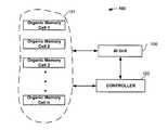
- FIG. 1is a block diagram of a system that controls a programming of a memory cell with functioning zones, in accordance with an aspect of the present invention.
- FIG. 2illustrates a schematic programming system for a memory cell, according to one aspect of the present invention.
- FIG. 3illustrates a particular programming circuit for a memory cell having two electrodes.
- FIG. 4illustrates graphs associated with voltage-time and current-time for various programming states of a memory cell according to one aspect of the present invention.
- FIG. 5illustrates an exemplary methodology for programming a memory cell in accordance with an aspect of the present invention.
- FIG. 6 aillustrates a programming circuit according to a further aspect of the present invention for a memory cell with functional zones employing three upper electrodes.
- FIG. 6 billustrates a schematic block diagram of a diode operating as part of a memory cell for a data processing system in accordance with an aspect of the present invention.
- FIGS. 7 a and 7 billustrate various structures of memory devices in accordance with an aspect of the present invention.
- FIG. 8is a graph depicting the effect of an intrinsic electric field on an interface between a passive layer and a polymer layer in accordance with an aspect of the present invention.
- FIG. 10is a graph illustrating charge carrier distribution of an exemplary memory cell in accordance with an aspect of the present invention.
- FIG. 11is a graph illustrating charge carrier distribution of an exemplary memory cell in accordance with an aspect of the present invention.
- FIG. 12is a graph illustrating charge carrier distribution of an exemplary memory cell in accordance with an aspect of the present invention.
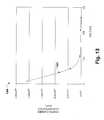
- FIG. 13is a graph illustrating charge carrier concentration at the interface of an exemplary memory cell in accordance with an aspect of the present invention.
- FIG. 14is a graph illustrating charge carrier concentration at the interface of an exemplary memory cell in accordance with an aspect of the present invention.
- FIG. 15is a schematic diagram depicting an organic memory device in various states in accordance with an aspect of the present invention.
- FIG. 16is a graph illustrating I-V characteristics for an organic memory device in accordance with an aspect of the present invention.
- FIG. 1a schematic block diagram illustrating a system 100 that actively programs a plurality of n memory cells 101 , (n being an integer) each with a functional layer, according to one aspect of the present invention.
- the systemincludes a controller component 102 that can write/read/erase any of the memory cells operatively connected thereto by employing a controlled operation.
- each memory cell of the groupcan accept and maintain a plurality of states, in contrast to a conventional memory device that is limited to two states (e.g., off or on). Accordingly, each memory cell can employ varying degrees of conductivity to identify additional states.
- the memory cellscan have a very highly conductive state (very low impedance state), a highly conductive state (low impedance state), a conductive state (medium level impedance state), and a non-conductive state (high impedance state) thereby enabling the storage of multiple bits of information in a single memory cell, such as 2 or more bits of information or 4 or more bits of information (e.g., 4 states providing 2 bits of information, 8 states providing 3 bits of information and the like.)
- Switching a memory cell of the group 101 to a particular stateis referred to as programming or writing.
- programmingcan be accomplished by applying a particular voltage (e.g., 9 volts, 2 volts, 1 volts, . . .
- Such particular voltagealso referred to as a threshold voltage
- a threshold voltagecan vary according to a respective desired state and is generally substantially greater than voltages employed during normal operation.
- the threshold valuevaries depending upon a number of factors including the identity of the materials that constitute the particular memory cell to be programmed, the thickness of the various layers, and the like.
- an external stimulisuch as an applied, voltage or electric field that exceeds a threshold value (e.g. “on” state) permits the writing, reading, or erasing information into/from the memory cells 101 ; whereas the absence of the external stimuli that exceeds a threshold value (“off” state) prevents a write or erase of information into/from the memory cells 101 .
- a threshold valuee.g. “on” state
- a voltage or electric fielde.g., 2 volts, 1 volts, 0.5 volts
- an impedance measurementcan be performed which, therein determines which operating state one or more of the memory cells are in (e.g., high impedance, very low impedance, low impedance, medium impedance, and the like).
- the impedancerelates to, for example, “on” (e.g., 1) or “off” (e.g., 0) for a dual state device, or to “00”, “01”, “10”, or “11” for a quad state device. It is appreciated that other numbers of states can provide other binary interpretations.
- a negative voltage or a polarity opposite the polarity of the writing signal that exceeds a threshold valuecan be applied.
- the system 100 in connection with such active programmingcan employ various artificial intelligence based schemes 106 for carrying out various aspects thereof. For example, a process for learning explicitly or implicitly when a particular memory device should be provided with a signal that initiates a write, read, or erase, can be facilitated via an automatic classification system and process. In addition, tracing of an affected feature associated (e.g. current and/or voltage) with a particular memory cell can be accomplished via such artificial intelligence component 106 . Classification can employ a probabilistic and/or statistical-based analysis (e.g., factoring into the analysis utilities and costs) to prognose or infer an action on a particular memory cell that is desired to be automatically performed. For example, a support vector machine (SVM) classifier can be employed.
- SVMsupport vector machine
- a componentcan also be, but is not so limited, a process running on a processor, a processor, an object, an executable, a thread of execution, a program, and/or a computer.
- an application running on a server and the servercan be a component.
- One or more componentscan reside within a process and/or thread of execution and a component can be localized on one computer and/or distributed between two or more computers. It is to be appreciated that filters, minifilters, filter managers, classifiers, models, order groups and other various items are components.
- the memory set 101can be an array of memory cells that is generally formed on a silicon based wafer, and includes a plurality of rows, referred to as bitlines, and a plurality of columns, referred to as wordlines. Such bit line and wordlines can be connected to the top and bottom metal layers of an individual memory cell's electrode. The intersection of a bitline and a wordline constitutes the address of a particular memory cell, wherein data can be stored in the memory cells (e.g., as a 00 or a 01, 10, 11 for a two bit memory cell operation) by choosing and sending signals via the artificial intelligence component 106 to the appropriate columns and rows in the array.
- a signale.g. current and/or voltage
- CAScolumn address strobe
- RASrow address strobe
- a reverse voltagecan be directed to the desired memory cell address.
- the present inventionhas application to any number of memory cells and is not to be limited to any particular configuration, arrangement and/or number of memory cells.
- FIG. 2illustrates a schematic programming system for a memory cell with a functional zone wherein the controller comprises a microprocessor 220 .
- the microprocessor 220can be part of a suitably programmed general purpose computer of a network and can also be implemented by employing a plurality of separated dedicated programmable integrated or other logic devices. Other information display devices (e.g. monitors, displays and the like), as well as user input devices can be operatively connected to the input/output of such processor.
- the processor 220can actively trace and control a program state of the memory cell 210 .
- the microprocessor system 220can provide a programming signal, e.g.
- a voltage applied to the memory element 210and detect an ensuing electric current that flows through it.
- the voltagecan be removed, and programming stopped. Such can be accomplished by comparing the current via a comparator 224 to reference values. Accordingly, the memory cell 210 can be programmed to a predetermined state. Likewise, by applying a reverse signal, e.g. reverse voltage, information of that state can be erased from such memory cell.
- a reverse signale.g. reverse voltage
- a ballast resistor 360is operatively connected to the memory cell 340 , and has a resistance that increases rapidly with increases in current through the resistor 360 , thereby tending to maintain an essentially constant current despite any variations in the line voltages.
- Registering devices 370 and 380can monitor circuit conditions during various programming stages of the memory cell 340 .
- the value of the current flowing through the memory cellcan be obtained by measuring voltage on the ballast resistor 360 , and such registering device can include voltmeters, oscillographs, recorders and other devices employed for monitoring circuit conditions at any moment.
- the generator 320forms an initial voltage pulse that exceeds a threshold value required for programming a memory cell.
- FIG. 4illustrates associated voltage-time and current-time graphs of such a methodology for writing a two bit memory cell operation. Voltage levels “Z” and “Y” depict an initial voltage pulse and a threshold voltage respectively.
- the values of the current flowing through the memory cell 340can then be obtained by measuring voltage on the ballast resistor 360 . As such, current flowing through the memory cell can be controlled such that the various electric current pulse states correspond to respective bits of information, written in to the memory cell. For example and as depicted in FIG.
- electric current level “A”can designate a value “00”
- electric current level “B”can designate a value “01”
- electric current level “C”can designate a value “10”
- electric current level “D”can designate the value “11”, all which are programmable into the memory cell 340 .
- the write programmingis complete, and the programming voltage switched off.
- a reading voltage “X” that is lower than the threshold voltage value “Y”is generated via the generator 320 .
- the resistance of the memory cell 340can then be estimated, and an electric current flowing through it obtained.
- Such electric currentcan then correspond to a reference electric current, to verify a programmed state of the memory cell.
- the generator 320creates a negative voltage pulse W, which can create a current, controlled to reach an erase threshold value flowing through the memory cell.
- the controlled valuecan be an intensity of light (optical programming when light sensor/emitter layers are employed), or amount of time that the memory cell is subject to an external stimulus and/or signal.
- intensity of lightoptical programming when light sensor/emitter layers are employed
- amount of time that the memory cell is subject to an external stimulus and/or signalcan also depend upon the structure of a particular memory cell, and material employed in its fabrication, as for the particular memory structure illustrated by FIG. 3, it may be necessary to return the cell to its initial state and erase recorded information before a further write operation can be performed.
- FIG. 5a flow diagram illustrates a methodology 500 for programming a memory cell according to one or more aspects of the present invention.
- the methodologybegins at 502 where general initializations are performed. Such initializations can include, but are not limited to, establishing pointers, allocating memory, setting variables, establishing communication channels and/or instantiating one or more objects.
- the memory cell to be programmedreceives an external stimulus. Such an external stimulus can be supplied via a control component, and can change an electrical and/or optical property(ies) associated with the memory cell.
- the control componentcan further monitor/regulate the external stimulus, and thereby control the influenced property of the memory cell.
- the value of property thus affectedcan be obtained (e.g.
- the obtained valueis compared (e.g. via a comparator of the control system) to a reference threshold determined for that particular property.
- a reference thresholdcan set an upper limit associated with a particular programming state for the memory cell having a functional zone to be programmed. It is to be appreciated that other electrical/optical features that are dependent on the affected property can also be compared to respective predetermined values, and employed as reference criteria for verifying the program state.
- the processprogresses to comparing step 510 , if the value of the affected property exceeds or is equal to the reference threshold, then programming for such state is considered complete.
- the methodthen removes the external stimulus at 512 , and ends at 514 . Otherwise, the program returns to subjecting the memory cell to a new stimulus.
- the reference thresholdcan set a lower limit associated with a particular programming state.
- the threshold referencecan also constitute a range, and the comparison step verifying whether the affected property of the memory cell falls within the range or not. While the exemplary method is illustrated and described herein as a series of blocks representative of various events and/or acts, the present invention is not limited by the illustrated ordering of such blocks.
- the memory cellcan be subject to a stimulus that facilitates reading bits of information, as opposed to writing or erasing.
- not all illustrated blocks, events or actsmay be required to implement a methodology in accordance with the present invention.
- the exemplary method and other methods according to the inventionmay be implemented in association with programming the memory cell illustrated and described herein, as well as in association with other systems and apparatus not illustrated or described.
- FIG. 6 aillustrates a circuit that programs a memory cell having a functioning layer according to a further aspect of the present invention.
- the memory cell 620includes a top electrode comprising of three partial electrode components; A, B, C, which together with a bottom electrode, sandwich a selective conductive layer, as will be described infra.
- the circuitalso includes a controller 640 that can provide a controllable electrical current, or voltage level (e.g. a programmable current or voltage) during information writing and/or recording of the memory cell 620 , while at the same time an electric resistance between end electrode elements A, C is being controlled.
- a controllable electrical current, or voltage levele.g. a programmable current or voltage
- writing of informationcan, for example, be considered complete when a controlled electrical resistance value associated with the memory cell reaches a predetermined or preset value. Thereafter, the applied voltage can be switched off. Similarly, information can be read by subjecting the memory cell to low voltage pulses to measure the electrical resistance between elements A, C.
- the structure for the electrodes of the memory cellenables two modes (zero, non-zero) for reading information when voltage is applied between the bottom electrode and the upper electrode element B.
- such structurefacilitates a control accuracy of programming the memory cell, as the write and read circuits are isolated and decoupled.
- control of a resistance value at various points of the memory cellcan generally be improved.
- FIG. 6 billustrates a schematic block diagram of data processing system 670 with a memory cell having a diode in accordance with an aspect of the present invention.
- Controller 660which can include a logic component can program the memory cell 669 according to methodologies discussed supra.
- the diode 663can be an optical diode positioned between electrodes 661 and 662 of a memory cell 669 having a passive layer 664 .
- the diodeitself can form a layer and comprise electrode layer(s) with organic and/or nom-organic material.
- the memory cell 669can be programmed by a signal that applies a forward bias (or a reverse bias).
- the controller 660can apply a reverse bias voltage that exceeds the diode 663 breakdown voltage and create an electric field (or a current) between electrodes 661 , 662 . It is to be appreciated that that the diode 663 can also be separate of the memory cell structure 669 .
- the electrodescan be comprised of a conductive material such as, aluminum, chromium, copper, germanium, gold, magnesium, manganese, indium, iron, nickel, palladium, platinum, silver, titanium, zinc, alloys thereof, indium-tin oxide, polysilicon, doped amorphous silicon, metal silicides, and the like.
- a conductive materialsuch as, aluminum, chromium, copper, germanium, gold, magnesium, manganese, indium, iron, nickel, palladium, platinum, silver, titanium, zinc, alloys thereof, indium-tin oxide, polysilicon, doped amorphous silicon, metal silicides, and the like.
- Exemplary alloys that can be utilized for the conductive materialinclude Hastelloy®, Kovar®, Invar, Monel®, Inconel®, brass, stainless steel, magnesium-silver alloy, and various other alloys.
- the thickness of the electrodescan vary depending on the implementation and the memory device being constructed. However, some exemplary thickness ranges include about 0.01 ⁇ m or more and about 10 ⁇ m or less, about 0.05 ⁇ m or more and about 5 ⁇ m or less, and/or about 0.1 ⁇ m or more and about 1 ⁇ m or less.
- the electrodescan be placed in an alternating fashion among various layers of for example semiconductor layers, polymer layers, and passive layers.
- the active layer 708 and the passive layer 706 of FIG. 7 aare collectively referred to as a selectively conductive media or selectively conductive layer.
- the conductive properties of this mediae.g., conductive, non-conductive, semi-conductive
- the active layer 708can be comprised of a conjugated material 750 , such as a small organic molecule and a conjugated polymer.
- a polymer backbone of the conjugated organic polymermay extend lengthwise between the electrodes 704 and 710 (e.g., generally substantially perpendicular to the inner, facing surfaces of the electrodes 704 and 710 ).
- the conjugated organic moleculecan be linear or branched such that the backbone retains its conjugated nature.
- Such conjugated moleculesare characterized in that they have overlapping 7 r orbitals and that they can assume two or more resonant structures.
- the conjugated nature of the conjugated organic materialscontributes to the controllably conductive properties of the selectively conductive media.
- the conjugated organic materialhas the ability to donate and accept charges (holes and/or electrons).
- the conjugated organic moleculehas at least two relatively stable oxidation-reduction states. The two relatively stable states permit the conjugated organic polymer to donate and accept charges and electrically interact with the conductivity facilitating compound.
- the organic materialmay be cyclic or acyclic.
- the organic materialself assembles between the electrodes during formation or deposition.
- conjugated organic polymersinclude one or more of polyacetylene (cis or trans); polyphenylacetylene (cis or trans); polydiphenylacetylene; polyaniline; poly(p-phenylene vinylene); polythiophene; polyporphyrins; porphyrinic macrocycles, thiol derivatized polyporphyrins; polymetallocenes such as polyferrocenes, polyphthalocyanines; polyvinylenes; polystiroles; and the like.
- the properties of the organic materialcan be modified by doping with a suitable dopant.
- the organic layer 750has a suitable thickness that depends upon the chosen implementations and/or the memory device being fabricated. Some suitable exemplary ranges of thickness for the organic polymer layer 750 are about 0.001 ⁇ m or more and about 5 ⁇ m or less, about 0.01 ⁇ m or more and about 2.5 ⁇ m or less, and about a thickness of about 0.05 ⁇ m or more and about 1 ⁇ m or less.
- the organic layer 750can be formed via a number of suitable techniques.
- One suitable technique that can be utilizedis a spin-on technique which involves depositing a mixture of the material and a solvent, and then removing the solvent from the substrate/electrode.
- Another suitable techniqueis chemical vapor deposition (CVD).
- CVDincludes low pressure chemical vapor deposition (LPCVD), plasma enhanced chemical vapor deposition (PECVD), and high density chemical vapor deposition (HDCVD). It is not typically necessary to functionalize one or more ends of the organic molecule in order to attach it to an electrode/passive layer. Sometime it may have a chemical bond formed between the conjugated organic polymer and the passive layer 706 .
- the passive layer 706 of FIG. 7 acontains at least one conductivity facilitating compound that contributes to the controllably conductive properties of the selectively conductive media.
- the conductivity facilitating compoundhas the ability to donate and accept charges (holes and/or electrons).
- the conductivity facilitating compoundhas at least two relatively stable oxidation-reduction states. The two relatively stable states permit the conductivity facilitating compound to donate and accept charges and electrically interact with the organic layer 750 .
- the particular conductivity facilitating compound employedis selected so that the two relatively stable states match with the two relatively stable states of the conjugated organic molecule of layer 750 .
- the passive layer 706is operative to transport charge from the first electrode 704 to the interface between the organic layer 750 and the passive layer 706 . Additionally, the passive layer 706 facilitates charge carrier (e.g., electrons or holes) injection into the organic layer 750 and increases the concentration of the charge carrier in the organic layer resulting in a modification of the conductivity of the organic layer 750 . Furthermore, the passive layer 706 can also store opposite charges in the passive layer 706 in order to balance the total charge of the device. In addition, the passive layer 706 can in some instances act as a catalyst when forming the organic layer 750 .
- charge carriere.g., electrons or holes
- the backbone of the conjugated organic moleculemay initially form adjacent the passive layer 706 , and grow or assemble away and substantially perpendicular to the passive layer surface.
- the backbones of the conjugated organic moleculemay be self aligned in a direction that traverses the two electrodes.
- Examples of conductivity facilitating compounds that may make up the passive layer 706include, but are not limited to, one or more of copper sulfide (Cu 2 S, CuS), copper oxide (CuO, Cu 2 O), manganese oxide (MnO 2 ), titanium dioxide (TiO 2 ), indium oxide (I 3 O 4 ), silver sulfide (Ag 2 S), iron oxide (Fe 3 O 4 ), and the like.
- the passive layer 706may be grown using oxidation techniques, formed via gas phase reactions, or deposited between the electrodes. It is to be appreciated that the invention is not so limited and other conducting and/or semi conducting materials can also be employed. In addition, other layer structures such as active layers, barrier layers, functioning zones can be employed in fabricating the memory cell.
- the passive layer 706has a suitable thickness that can vary based on the implementation and/or memory device being fabricated. Some examples of suitable thicknesses for the passive layer 706 are as follows: a thickness of about 2 ⁇ or more and about 0.1 ⁇ m or less, a thickness of about 10 ⁇ or more and about 0.01 ⁇ m or less, and a thickness of about 50 ⁇ or more and about 0.005 ⁇ m or less.
- the organic layer 750is generally thicker than the passive layer 706 .
- the thickness of the organic layeris from about 0.1 to about 500 times greater than the thickness of the passive layer. It is appreciated that other suitable ratios can be employed in accordance with the present invention.
- various other electro conductive and optically transparent materialscan also be employed, e.g. when formation of elements such as; diodes, and photo sensors, photo diodes, photo resistance, or light emitting structures are desired.
- light emitting layer 720e.g. comprising polyphenil vinylene
- light sensing layer 740are separated by transparent electrode 725 (e.g. comprising indium oxide.)
- transparent electrode 725e.g. comprising indium oxide.
- Such structurecan facilitate an optical programming (e.g. writing and/or erasing) of the organic memory cell.
- the light emitting layer 720if subjected to a voltage can generate light as a function of the impedance state of the organic memory cell.
- Such emitted lightcan then be received by the light sensing material 740 , and depending on received light properties (e.g. amount, intensity, polarity, phase and the like), various states can be programmed in the memory cell.
- a memory structure employing a plurality of electrodes and passive/active layersfacilitates decoupling of the of Read/Write circuits, e.g. a diode structure, photo resistance, photo sensor elements and the like.
- various diode componentscan be formed (e.g. via employing additional layers of electrodes, conductive/semi conductive material) as part of the memory cell structure.
- Electrodes 710 and 704can flow between electrodes 710 and 704 through the selectively conductive media, and/or the functional zone based on a voltage state applied to the electrodes.
- holescan flow from the first electrode 704 to second electrode 710 if the organic layer 750 is p-type conductor, or both electrons and holes flow in the organic layer if it can be both n and p type with proper energy band match with 706 and 710 .
- currentflows from the first electrode 704 to the second electrode 710 via the selectively conductive media.
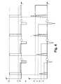
- FIG. 7 billustrates various layers incorporated as part of the structures of memory cells with two electrodes, according to exemplary aspects of the present invention.
- the memory cell 782has a three layered structure, which consists of two electrodes 783 , 784 and a functional zone 786 sandwiched there between.
- a functional zone 786can further include various alternating active, barrier and passive layers; such as 787 , 788 , 789 respectively.
- the barrier layer 788can be comprised of material such as Li 3 N deposited via a CVD process to an exemplary thickness of approximately 50 ⁇ .
- each layercan comprise further sub layers, as illustrated by the memory cell structure 790 , wherein the active layer itself comprises an active layer 1 and active layer 2 .
- the active layeritself comprises an active layer 1 and active layer 2 .
- other arrangements for stacking the active, passive, and barrier layerse.g. 796 , 797 , and 798 ) are possible, and are within the realm of the present invention.
- conductive polymeris used as organic material, and CuS is used as passive layer material.
- CuSis used as passive layer material.
- the copper in CuSis at its highest oxidation state Cu(II). It has relatively strong capability to gain electrons from a contacting polymer and yields the following equation:
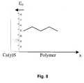
- FIG. 8is a graph depicting the effect of an intrinsic electric field on an interface between Cu(y)S (with y accepting a suitable value e.g. from 1 to 2) and a polymer is provided.
- the oxidized polymer(Polymer + ) is the charge carrier when external field is applied.
- the conductivity of polymeris determined by its concentration and its mobility.
- V ( x )qN p ( d p x ⁇ x 2 /2)/ ⁇ (3)
- N pis the average concentration of charge carrier
- ⁇is the dielectric constant of the polymer
- d pis the width of the charge depletion.
- Vis the external field voltage applied. For forward voltage, it is “ ⁇ ” sign. For the reverse voltage, it is “+” sign.
- Ddiffusion constant of the charge carrier
- Ethe electric field at x. If there is no current, the carrier distribution is:
- the final characteristic, retention timerefers to the fact that a forward voltage produces more charge carrier and the charge carrier accumulates more on the other end of the passive (CuS) layer (away from the organic polymer).
- this charge carrier concentrationwill be set back once the voltage is removed, which includes two processes: charge carrier diffusion toward the CuS layer and charge carrier recombination on the interface.
- Fick's Lawcan describe the 1st process, charge carrier diffusion toward the CuS layer.
- the charge carrier recombinationcan be described as follows:
- the retention timeis the time required to redistribute the charge carrier to the original state. It is likely that the reaction rate is relatively faster than diffusion rate. Therefore, the retention time can be substantially determined by the diffusion process only.
- An exemplary memory cellis considered herein with respect to the equations 1-9 discussed supra and illustrated in FIGS. 9 - 14 .
- Six typical casesare calculated to illustrate electrical operation of an organic memory device in accordance with an aspect of the present invention.
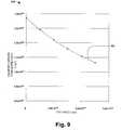
- FIG. 9depicts a graph 900 of charge carrier distribution 901 of the exemplary memory cell as a function of distance from the CuS and organic polymer interface in accordance with an aspect of the invention.
- the charge carrier concentration 901is shown as being a decreasing function of distance (x) from the interface.
- the charge carrier concentration 901is derived utilizing Eq. 6 with a constant field assumption. However, the points shown are independent of the constant field assumption.
- FIG. 10another graph 1000 illustrating charge carrier distribution 1001 for the exemplary organic memory cell is depicted in accordance with an aspect of the present invention.
- the CuS endhas a higher voltage than the other end (organic polymer).
- Thisdrives the charge carrier away from CuS layer and leads to charge carrier concentration that has an increase function of x. Even at lowest concentration p(0), it is not a small value for this case.
- Thisexplains why the polymer is a good conductor when forward voltage is applied.
- itis Eq. 6 with constant electric field model used for the plot. The points demonstrated are independent of constant electric field assumption.
- FIG. 11depicts yet another graph 1100 of charge carrier distribution 1101 of the exemplary memory cell as a function of distance from the CuS and organic polymer interface in accordance with an aspect of the invention.
- the charge carrieris concentrated at the CuS polymer interface and drops quickly to small concentration when it is away from the interface, which describes why the organic memory cell becomes non-conductive when high reversed voltage applied.
- Eq. 6 with constant electric field modelis assumed for the plot. The points demonstrated are independent of this assumption.
- FIG. 12another graph 1200 that depicts charge carrier distribution 1201 of the exemplary memory cell as a function of distance in accordance with an aspect of the present invention is provided.
- current flux J>0the charge carrier is still an increase function of x because the forward voltage drives the charge carrier away from CuS interface.
- One important pointis that the lowest concentration p(x) is at interface.
- FIG. 13depicts yet another graph 1300 of charge carrier concentration at interface 1301 of the exemplary memory cell as function of forward voltage V.
- This modelassumes the electric field in the cell is constant. Therefore, the voltage V(x) is described as a linear function.
- This modelis applicable when the diffusion constant of the polymer is small and there is constant electric resistance.
- the charge carrier concentration at interfaceis derived as function of voltage. It is noted that p 0 (V) tends to be constant after forward voltage is large enough and the current is controlled by the charge carrier not charge injection at the interface.
- This Eq. 10shows that limiting p(0) is an increase function of thickness ratio between CuS layer and polymer layer.
- FIG. 14illustrates another graph 1400 that depicts charge carrier concentration at the interface 1401 of the exemplary memory cell as function of forward voltage Vin accordance with an aspect of the present invention is provided.
- p(0)is a function of forward voltage, current J, which may or may not be >0, and a step potential function model.
- This modelassumes the voltage V(x) function can be described by a step function. The model is applicable when the diffusion constant of the polymer is very large. Therefore, the electric resistance in the cell is trivial.
- the charge carrier concentration at interfaceis derived as the function of voltage. It is noted that in FIG. 14 that p 0 (V) tends to be zero after forward voltage is large enough.
- p(0)is an increase function of thickness ratio between CuS layer and polymer layer.
- the flux measuredis determined by charge carrier drift when limiting flux is in the polymer.
- the function to describe the charge carrier concentrationis p(x).
- another functionis employed to describe the charge carrier concentration p(x).
- the initial charge carrier concentration p(x)has a relatively substantially smaller value than other regions. Therefore, J is still determined by p(0).
- boundary conditionsUnlike semiconductors, it is just applicable to the concentration at interface, not everywhere. This boundary condition limits the total amount of the charge carrier produced in the cell.
- the equations supra (e.q. 1-7) and the FIGS. 11 - 14describe and model behavior of organic memory devices.
- This modelcan be employed to explain measured data and can be for other passive layer materials aside from CuS. Additionally, the model can be used to think about how to improve retention and response time and to design the other devices such as transistor. Further, the model can be employed to develop various threshold voltages that set conductivity levels (e.g., set states), read conductivity levels and erase the conductivity levels thus performing memory device operations of writing or programming, reading and erasing.
- FIG. 15is a schematic diagram that illustrates an organic memory device 1500 in various states in accordance with an aspect of the present invention.
- the device 1500is depicted in a first “off” state 1501 , an “on” state 1502 , and a second “off” state 1503 . It is appreciated that memory devices formed in accordance with the present invention can have other states than those depicted in FIG. 15.
- the organic memory device 1500comprises a top electrode 1504 , a bottom electrode 1506 and a selectively conductive layer 1508 comprising an organic layer (e.g., PPA) and at least one passive layer (e.g., CuS).
- PPAorganic layer
- CuSpassive layer
- the electrons 1510collect in the selectively conductive layer 1508 near the bottom electrode 1506 .
- the electrons 1510are uniformly distributed thereby indicating an on state.
- the electronscollect in the selectively conductive layer 1508 near the top electrode 1504 .
- FIG. 16is a graph 1600 that illustrates I-V characteristics for an organic memory device of the present invention. It can be seen that from state 1, which indicates “off”, the device can be modified to be in state 2, which indicates “on”, by applying a positive voltage of 2V. Additionally, it can be seen that whilst in state 1, the organic memory device has a high impedance and low conductance. Subsequently, the device 1500 can be modified to change from state 2 to state 1 by application of a negative voltage, therein causing a reverse current until the state 1 is obtained.
- the organic memory cells/devicesare useful in any device requiring memory.
- the organic memory devicesare useful in computers, appliances, industrial equipment, hand-held devices, telecommunications equipment, medical equipment, research and development equipment, transportation vehicles, radar/satellite devices, and the like.
- Hand-held devices, and particularly hand-held electronic devicesachieve improvements in portability due to the small size and light weight of the organic memory devices. Examples of hand-held devices include cell phones and other two way communication devices, personal data assistants, palm pilots, pagers, notebook computers, remote controls, recorders (video and audio), radios, small televisions and web viewers, cameras, and the like.
Landscapes
- Engineering & Computer Science (AREA)
- Chemical & Material Sciences (AREA)
- Computer Hardware Design (AREA)
- Nanotechnology (AREA)
- Crystallography & Structural Chemistry (AREA)
- Theoretical Computer Science (AREA)
- Mathematical Physics (AREA)
- Physics & Mathematics (AREA)
- Manufacturing & Machinery (AREA)
- Materials Engineering (AREA)
- Semiconductor Memories (AREA)
- Nitrogen And Oxygen Or Sulfur-Condensed Heterocyclic Ring Systems (AREA)
- Read Only Memory (AREA)
Abstract
Description
- This application is a Continuation-in-Part of PCT application PCT/RU01/00334 filed Aug. 13, 2001.[0001]
- The present invention relates generally to memory devices and, in particular, to programming a memory device having a functional layer via a controlled operation.[0002]
- The proliferation and increased usage of portable computer and electronic devices has greatly increased demand for memory cells. Digital cameras, digital audio players, personal digital assistants, and the like generally seek to employ large capacity memory cells (e.g., flash memory, smart media, compact flash, or the like). Memory cells can be typically employed in various types of storage devices. Storage devices include long term storage mediums such as, for example, hard disk drives, compact disk drives and corresponding media, digital video disk (DVD) drives, and the like. The long term storage mediums typically store larger amounts of information at a lower cost, but are slower than other types of storage devices. Storage devices also include memory devices which are often, but not always, short term storage mediums.[0003]
- Also, memory cells can generally be subdivided into volatile and non-volatile types. Volatile memory cells usually lose their information if they lose power and typically require periodic refresh cycles to maintain their information. Volatile memory cells include, for example, random access memory (RAM), DRAM, SRAM and the like. Non-volatile memory cells maintain their information whether or not power is maintained to the devices. Examples of non-volatile memory cells include; ROM, programmable read only memory (PROM), erasable programmable read only memory (EPROM), electrically erasable programmable read only memory (EEPROM), flash EEPROM the like. Volatile memory cells generally provide faster operation at a lower cost as compared to non-volatile memory cells. Nonetheless, to retain the information, the stored data typically must be refreshed; that is, each capacitor must be periodically charged or discharged to maintain the capacitor's charged or discharged state. The maximum time allowable between refresh operations depends on the charge storage capabilities of the capacitors that make up the memory cells in the array. The memory device manufacturer typically specifies a refresh time that guarantees data retention in the memory cells.[0004]
- As such, each memory cell in a memory device can be accessed or “read”, “written”, and “erased” with information. The memory cells maintain information in an “off” or an “on” state (e.g., are limited to 2 states), also referred to as “0” and “I”. Typically, a memory device is addressed to retrieve a specified number of byte(s) (e.g., 8 memory cells per byte). For volatile memory devices, the memory cells must be periodically “refreshed” in order to maintain their state. Such memory devices are usually fabricated from semiconductor devices that perform these various functions and are capable of switching and maintaining the two states. The devices are often fabricated with inorganic solid state technology, such as, crystalline silicon devices. A common semiconductor device employed in memory devices is the metal oxide semiconductor field effect transistor (MOSFET).[0005]
- Because of the increasing demand for information storage, memory device developers and manufacturers are constantly attempting to increase speed and storage retrieval for memory devices (e.g., increase write/read speed). At the same time, to reach high storage densities, manufacturers typically focus on scaling down semiconductor device dimensions (e.g., at sub-micron levels). Nonetheless, as the size of inorganic solid state devices decreases and integration increases, sensitivity to alignment tolerances can also increase making fabrication markedly more difficult. Moreover, formation of features at small minimum sizes does not imply that the minimum size can be used for fabrication of working circuits. Furthermore, such shrinkage for inorganic non-volatile memory cells, can be particularly difficult to do while maintaining low costs. Accordingly, silicon-based devices are approaching their fundamental physical size limits, and further device shrinking and density increasing may be limited for such memory cells.[0006]
- Therefore, there is a need to overcome the aforementioned deficiencies associated with conventional memory cells and their programming.[0007]
- The following presents a simplified summary of the invention in order to provide a basic understanding of one or more aspects of the invention. This summary is not an extensive overview of the invention. It is intended to neither identify key or critical elements of the invention, nor to delineate the scope of the present invention. Rather, the sole purpose of this summary is to present some concepts of the invention in a simplified form as a prelude to the more detailed description that is presented hereinafter.[0008]
- The present invention provides for systems and methods for programming a memory cell(s) with functional zone(s)/layer(s), or selective conductive layers, by employing a controlled operation. The functional zone can include active, and/or passive and/or barrier layers, as described in more detail infra. Such programming can typically provide for stability, viability and fast switching of a memory cell's operation at a multi-bit level. According to one aspect of the present invention, an “active” mode of programming is employed to program a memory cell with a functional zone—(in contrast to a “passive” method that can employ a load resistance during an “ON” state to limit a flowing current, with the memory cell exhibiting an impedance equal to the value of the load resistance.) Initially, the memory cell to be programmed receives an external stimulus. Such an external stimulus can be supplied via a control component, and can influence an electrical and/or optical property(ies) associated with the functional zone of the memory cell to be programmed. The control component can further control the external stimulus, and thereby regulate and/or trace the influenced property of the memory cell. The value of such property thus affected is then compared to a reference threshold, which is set for that particular property—other electrical/optical features that are dependent on the affected property can also be compared to respective predetermined values to effectuate a corresponding programming state. Based on such comparison, the programming can then be verified, and the external stimulus removed upon completion of the programming state.[0009]
- For example, the reference threshold can designate a lower limit associated with a particular programming state for the memory cell. If the value of the affected property exceeds the reference threshold, then the cell is properly programmed for that particular state. The reference threshold can also set an upper limit, or include a range associated with that programming state.[0010]
- In one exemplary aspect of active mode programming according to the present invention, size of the current through the memory cell in an “ON” state is set by a control system that actively traces conditions for switching of the memory cell. The control system can further include an artificial intelligence component that can regulate, and/or monitor, state of the electric current/voltage applied to the memory cell during its programming and/or information recording/reading. Moreover, the artificial intelligence component can send verifying signal to the memory cell at various stages to verify its programmable state. Such signal can be in the form of an electric current and/or voltage. It is to be appreciated that such verification arrangement (e.g. for a write or erase) during, for example, switching from an “OFF” state to an “ON” state can depend on the particular structural design of the memory cell with the functional zone to be programmed, e.g. number of top electrodes.[0011]
- In an exemplary methodology according to the present invention, the control system can be a generator of a controllable voltage pulse coupled to a ballast resistor that modifies an incoming current/voltage to maintain programming conditions. The generator initially generates a voltage exceeding a threshold value associated with a particular programming state for the memory cell. Accordingly, an ensuing electric current pulse passing through the memory cell can then reach a predetermined value required for the writing mode, at which time the writing operation for the memory cell is considered complete. Subsequently, the generator switches to a reading mode and generates a reading voltage that is substantially lower than the threshold voltage value required for writing. Based on a value of the electric current flowing through the ballast resistor, the impedance of the memory cell can be estimated. Such resistance values can then be corresponded to specific bit information to facilitate a read thereof. In a related aspect of the present invention, erasing of the information occurs when the generator sends a negative voltage pulse with the controlled erasing current value reaching a preset value. The erase operation is considered complete when the controlled values of current and/or resistance values reach the preset level, whereupon the electric voltage is being turned off.[0012]
- The memory cell with a functioning zone to be such programmed can comprise of several electrodes stacked on top of each other, with alternating passive/active/barrier layers that constitute the functioning zone. Accordingly, the memory cell programming can be performed by applying voltages and —or controlling resistance values among selected electrodes of the memory cell.[0013]
- To the accomplishment of the foregoing and related ends, the invention, then, comprises the features hereinafter fully described. The following description and the annexed drawings set forth in detail certain illustrative aspects of the invention. However, these aspects are indicative of but a few of the various ways in which the principles of the invention may be employed. Other aspects, advantages and novel features of the invention will become apparent from the following detailed description of the invention when considered in conjunction with the drawings. To facilitate the reading of the drawings, some of the drawings may not have been drawn to scale from one figure to another or within a given figure.[0014]
- FIG. 1 is a block diagram of a system that controls a programming of a memory cell with functioning zones, in accordance with an aspect of the present invention.[0015]
- FIG. 2 illustrates a schematic programming system for a memory cell, according to one aspect of the present invention.[0016]
- FIG. 3 illustrates a particular programming circuit for a memory cell having two electrodes.[0017]
- FIG. 4 illustrates graphs associated with voltage-time and current-time for various programming states of a memory cell according to one aspect of the present invention.[0018]
- FIG. 5 illustrates an exemplary methodology for programming a memory cell in accordance with an aspect of the present invention.[0019]
- FIG. 6[0020]aillustrates a programming circuit according to a further aspect of the present invention for a memory cell with functional zones employing three upper electrodes.
- FIG. 6[0021]billustrates a schematic block diagram of a diode operating as part of a memory cell for a data processing system in accordance with an aspect of the present invention.
- FIGS. 7[0022]aand7billustrate various structures of memory devices in accordance with an aspect of the present invention.
- FIG. 8 is a graph depicting the effect of an intrinsic electric field on an interface between a passive layer and a polymer layer in accordance with an aspect of the present invention.[0023]
- FIG. 9 is a graph illustrating charge carrier distribution of an exemplary memory cell in accordance with an aspect of the present invention.[0024]
- FIG. 10 is a graph illustrating charge carrier distribution of an exemplary memory cell in accordance with an aspect of the present invention.[0025]
- FIG. 11 is a graph illustrating charge carrier distribution of an exemplary memory cell in accordance with an aspect of the present invention.[0026]
- FIG. 12 is a graph illustrating charge carrier distribution of an exemplary memory cell in accordance with an aspect of the present invention.[0027]
- FIG. 13 is a graph illustrating charge carrier concentration at the interface of an exemplary memory cell in accordance with an aspect of the present invention.[0028]
- FIG. 14 is a graph illustrating charge carrier concentration at the interface of an exemplary memory cell in accordance with an aspect of the present invention.[0029]
- FIG. 15 is a schematic diagram depicting an organic memory device in various states in accordance with an aspect of the present invention.[0030]
- FIG. 16 is a graph illustrating I-V characteristics for an organic memory device in accordance with an aspect of the present invention.[0031]
- The present invention is now described with reference to the drawings, wherein like reference numerals are used to refer to like elements throughout. In the following description, for purposes of explanation, numerous specific details are set forth in order to provide a thorough understanding of the present invention. It may be evident, however, that the present invention may be practiced without these specific details. In other instances, well-known structures and devices are shown in block diagram form in order to facilitate describing the present invention.[0032]
- Referring initially to FIG. 1, a schematic block diagram illustrating a[0033]
system 100 that actively programs a plurality ofn memory cells 101, (n being an integer) each with a functional layer, according to one aspect of the present invention. The system includes acontroller component 102 that can write/read/erase any of the memory cells operatively connected thereto by employing a controlled operation. Typically, each memory cell of the group can accept and maintain a plurality of states, in contrast to a conventional memory device that is limited to two states (e.g., off or on). Accordingly, each memory cell can employ varying degrees of conductivity to identify additional states. For example, the memory cells can have a very highly conductive state (very low impedance state), a highly conductive state (low impedance state), a conductive state (medium level impedance state), and a non-conductive state (high impedance state) thereby enabling the storage of multiple bits of information in a single memory cell, such as 2 or more bits of information or 4 or more bits of information (e.g., 4 states providing 2 bits of information, 8 states providing 3 bits of information and the like.) Switching a memory cell of thegroup 101 to a particular state is referred to as programming or writing. For example, programming can be accomplished by applying a particular voltage (e.g., 9 volts, 2 volts, 1 volts, . . . ) across selected layers of the functioning zone of the memory cell, as described in detail infra. Such particular voltage, also referred to as a threshold voltage, can vary according to a respective desired state and is generally substantially greater than voltages employed during normal operation. Thus, there is typically a separate threshold voltage that corresponds to respective desired states (e.g., “off”, “on” . . . ). The threshold value varies depending upon a number of factors including the identity of the materials that constitute the particular memory cell to be programmed, the thickness of the various layers, and the like. - As such, the presence of an external stimuli such as an applied, voltage or electric field that exceeds a threshold value (e.g. “on” state) permits the writing, reading, or erasing information into/from the[0034]
memory cells 101; whereas the absence of the external stimuli that exceeds a threshold value (“off” state) prevents a write or erase of information into/from thememory cells 101. - To read information from the[0035]
memory cells 101, a voltage or electric field (e.g., 2 volts, 1 volts, 0.5 volts) can be applied via the controller12. Subsequently, an impedance measurement can be performed which, therein determines which operating state one or more of the memory cells are in (e.g., high impedance, very low impedance, low impedance, medium impedance, and the like). As stated supra, the impedance relates to, for example, “on” (e.g., 1) or “off” (e.g., 0) for a dual state device, or to “00”, “01”, “10”, or “11” for a quad state device. It is appreciated that other numbers of states can provide other binary interpretations. To erase information written into thememory cells 101, a negative voltage or a polarity opposite the polarity of the writing signal that exceeds a threshold value can be applied. - The[0036]
system 100 in connection with such active programming can employ various artificial intelligence basedschemes 106 for carrying out various aspects thereof. For example, a process for learning explicitly or implicitly when a particular memory device should be provided with a signal that initiates a write, read, or erase, can be facilitated via an automatic classification system and process. In addition, tracing of an affected feature associated (e.g. current and/or voltage) with a particular memory cell can be accomplished via suchartificial intelligence component 106. Classification can employ a probabilistic and/or statistical-based analysis (e.g., factoring into the analysis utilities and costs) to prognose or infer an action on a particular memory cell that is desired to be automatically performed. For example, a support vector machine (SVM) classifier can be employed. Other classification approaches include Bayesian networks, decision trees, and probabilistic classification models providing different patterns of independence can be employed. Classification as used herein also is inclusive of statistical regression that is utilized to develop models of priority. As will be readily appreciated from the subject specification, the subject invention can employ classifiers that are explicitly trained (e.g., via a generic training data) as well as implicitly trained (e.g., via receiving extrinsic information) so that the classifier is used to automatically determine according to a predetermined criteria what action to perform, or which answer to return to a question. For example, with respect to SVM's that are well understood, SVM's are configured via a learning or training phase within a classifier constructor and feature selection module. A classifier is a function that maps an input attribute vector, x=(x1, x2, x3, x4, xn), to a confidence that the input belongs to a class—that is, f(x)=confidence (class). As used in this application, the terms “component” and “system” are also intended to refer to a computer-related entity, either hardware, a combination of hardware and software, software, or software in execution. For example, a component can also be, but is not so limited, a process running on a processor, a processor, an object, an executable, a thread of execution, a program, and/or a computer. By way of illustration, both an application running on a server and the server can be a component. One or more components can reside within a process and/or thread of execution and a component can be localized on one computer and/or distributed between two or more computers. It is to be appreciated that filters, minifilters, filter managers, classifiers, models, order groups and other various items are components. - The memory set[0037]101 can be an array of memory cells that is generally formed on a silicon based wafer, and includes a plurality of rows, referred to as bitlines, and a plurality of columns, referred to as wordlines. Such bit line and wordlines can be connected to the top and bottom metal layers of an individual memory cell's electrode. The intersection of a bitline and a wordline constitutes the address of a particular memory cell, wherein data can be stored in the memory cells (e.g., as a 00 or a 01, 10, 11 for a two bit memory cell operation) by choosing and sending signals via the
artificial intelligence component 106 to the appropriate columns and rows in the array. (e.g., via a column address strobe (CAS) and a row address strobe (RAS), respectively). As will be described infra, to write to a memory cell, a signal (e.g. current and/or voltage) can be sent to the appropriate column and row address to overcome a threshold voltage and/or current value associated with that particular memory cell location. Similarly, to erase an memory cell of such array, a reverse voltage can be directed to the desired memory cell address. The present invention has application to any number of memory cells and is not to be limited to any particular configuration, arrangement and/or number of memory cells. - FIG. 2 illustrates a schematic programming system for a memory cell with a functional zone wherein the controller comprises a[0038]
microprocessor 220. Themicroprocessor 220 can be part of a suitably programmed general purpose computer of a network and can also be implemented by employing a plurality of separated dedicated programmable integrated or other logic devices. Other information display devices (e.g. monitors, displays and the like), as well as user input devices can be operatively connected to the input/output of such processor. Theprocessor 220 can actively trace and control a program state of thememory cell 210. For example, themicroprocessor system 220 can provide a programming signal, e.g. a voltage applied to thememory element 210, and detect an ensuing electric current that flows through it. When such current is detected to be at a predetermined value that represents a particular resistance of thememory element 210, the voltage can be removed, and programming stopped. Such can be accomplished by comparing the current via acomparator 224 to reference values. Accordingly, thememory cell 210 can be programmed to a predetermined state. Likewise, by applying a reverse signal, e.g. reverse voltage, information of that state can be erased from such memory cell. - Referring now to FIG. 3 a circuit that programs a memory cell having a functional zone according to one aspect of the present invention is illustrated. The control system for such circuit includes a[0039]
generator 320 that can provide a controllable electrical current level (e.g. a programmable current) during information writing and/or recording of thememory cell 340. Thememory cell 340 includes two electrodes that sandwich various layers e.g. a selective conductive layer (functional layer) comprising an active layer (e.g. organic layer) and a passive layer, as will be explained infra. It is to be appreciated that the present invention is not so limited and other layers such as functioning zone layers; barrier layers; active/passive layers, and the like can also be employed with other aspects of the present invention. - A[0040]
ballast resistor 360 is operatively connected to thememory cell 340, and has a resistance that increases rapidly with increases in current through theresistor 360, thereby tending to maintain an essentially constant current despite any variations in the line voltages. Registeringdevices memory cell 340. For example, the value of the current flowing through the memory cell can be obtained by measuring voltage on theballast resistor 360, and such registering device can include voltmeters, oscillographs, recorders and other devices employed for monitoring circuit conditions at any moment. - According to one particular methodology of the present invention, the[0041]
generator 320 forms an initial voltage pulse that exceeds a threshold value required for programming a memory cell. For example, FIG. 4 illustrates associated voltage-time and current-time graphs of such a methodology for writing a two bit memory cell operation. Voltage levels “Z” and “Y” depict an initial voltage pulse and a threshold voltage respectively. The values of the current flowing through thememory cell 340 can then be obtained by measuring voltage on theballast resistor 360. As such, current flowing through the memory cell can be controlled such that the various electric current pulse states correspond to respective bits of information, written in to the memory cell. For example and as depicted in FIG. 4; electric current level “A” can designate a value “00”, electric current level “B” can designate a value “01”, electric current level “C” can designate a value “10”, and electric current level “D” can designate the value “11”, all which are programmable into thememory cell 340. - Next, and after the electric current pulse reaches the desired programmed state, the write programming is complete, and the programming voltage switched off. Similarly, to read bits of information from the[0042]
memory cell 340, a reading voltage “X” that is lower than the threshold voltage value “Y” is generated via thegenerator 320. Based on the amount of current flowing through theballast resistor 360 of FIG. 3, the resistance of thememory cell 340 can then be estimated, and an electric current flowing through it obtained. Such electric current can then correspond to a reference electric current, to verify a programmed state of the memory cell. Likewise, to erase information, thegenerator 320 creates a negative voltage pulse W, which can create a current, controlled to reach an erase threshold value flowing through the memory cell. It is to be appreciated that other properties besides voltage, current, or impedance can be employed to program a memory cell having a functioning zone. For example, the controlled value can be an intensity of light (optical programming when light sensor/emitter layers are employed), or amount of time that the memory cell is subject to an external stimulus and/or signal. Such can also depend upon the structure of a particular memory cell, and material employed in its fabrication, as for the particular memory structure illustrated by FIG. 3, it may be necessary to return the cell to its initial state and erase recorded information before a further write operation can be performed. - Turning to FIG. 5, a flow diagram illustrates a[0043]
methodology 500 for programming a memory cell according to one or more aspects of the present invention. The methodology begins at502 where general initializations are performed. Such initializations can include, but are not limited to, establishing pointers, allocating memory, setting variables, establishing communication channels and/or instantiating one or more objects. At504, the memory cell to be programmed receives an external stimulus. Such an external stimulus can be supplied via a control component, and can change an electrical and/or optical property(ies) associated with the memory cell. The control component can further monitor/regulate the external stimulus, and thereby control the influenced property of the memory cell. At506, the value of property thus affected can be obtained (e.g. calculated and/or measured). Subsequently at508, the obtained value is compared (e.g. via a comparator of the control system) to a reference threshold determined for that particular property. Such reference threshold can set an upper limit associated with a particular programming state for the memory cell having a functional zone to be programmed. It is to be appreciated that other electrical/optical features that are dependent on the affected property can also be compared to respective predetermined values, and employed as reference criteria for verifying the program state. - Next, the process progresses to comparing[0044]
step 510, if the value of the affected property exceeds or is equal to the reference threshold, then programming for such state is considered complete. The method then removes the external stimulus at512, and ends at514. Otherwise, the program returns to subjecting the memory cell to a new stimulus. It is to be appreciated that the reference threshold can set a lower limit associated with a particular programming state. Moreover, the threshold reference can also constitute a range, and the comparison step verifying whether the affected property of the memory cell falls within the range or not. While the exemplary method is illustrated and described herein as a series of blocks representative of various events and/or acts, the present invention is not limited by the illustrated ordering of such blocks. For instance, some acts or events may occur in different orders and/or concurrently with other acts or events, apart from the ordering illustrated herein, in accordance with the invention. For example, the memory cell can be subject to a stimulus that facilitates reading bits of information, as opposed to writing or erasing. In addition, not all illustrated blocks, events or acts, may be required to implement a methodology in accordance with the present invention. Moreover, it will be appreciated that the exemplary method and other methods according to the invention may be implemented in association with programming the memory cell illustrated and described herein, as well as in association with other systems and apparatus not illustrated or described. - FIG. 6[0045]aillustrates a circuit that programs a memory cell having a functioning layer according to a further aspect of the present invention. The
memory cell 620 includes a top electrode comprising of three partial electrode components; A, B, C, which together with a bottom electrode, sandwich a selective conductive layer, as will be described infra. The circuit also includes acontroller 640 that can provide a controllable electrical current, or voltage level (e.g. a programmable current or voltage) during information writing and/or recording of thememory cell 620, while at the same time an electric resistance between end electrode elements A, C is being controlled. As described supra writing of information can, for example, be considered complete when a controlled electrical resistance value associated with the memory cell reaches a predetermined or preset value. Thereafter, the applied voltage can be switched off. Similarly, information can be read by subjecting the memory cell to low voltage pulses to measure the electrical resistance between elements A, C. As illustrated, the structure for the electrodes of the memory cell enables two modes (zero, non-zero) for reading information when voltage is applied between the bottom electrode and the upper electrode element B. In addition, such structure facilitates a control accuracy of programming the memory cell, as the write and read circuits are isolated and decoupled. Thus, for example control of a resistance value at various points of the memory cell can generally be improved. - FIG. 6[0046]billustrates a schematic block diagram of
data processing system 670 with a memory cell having a diode in accordance with an aspect of the present invention.Controller 660 which can include a logic component can program thememory cell 669 according to methodologies discussed supra. Thediode 663 can be an optical diode positioned betweenelectrodes memory cell 669 having apassive layer 664. The diode itself can form a layer and comprise electrode layer(s) with organic and/or nom-organic material. Accordingly, thememory cell 669 can be programmed by a signal that applies a forward bias (or a reverse bias). For example, in case of a reverse bias programming, thecontroller 660 can apply a reverse bias voltage that exceeds thediode 663 breakdown voltage and create an electric field (or a current) betweenelectrodes diode 663 can also be separate of thememory cell structure 669. - Referring now to FIGS. 7[0047]aand7bstructures of memory cells with various exemplary electrode arrangements and material are illustrated. Typically for such memory cells, upper and lower electrodes sandwich various other active, passive, functional zone, and polymer layers, which can also include various light emitting material, such as; light emitting structure, photo resistance, or photo sensors. The electrodes (e.g.704,710) can be comprised of a conductive material such as, aluminum, chromium, copper, germanium, gold, magnesium, manganese, indium, iron, nickel, palladium, platinum, silver, titanium, zinc, alloys thereof, indium-tin oxide, polysilicon, doped amorphous silicon, metal silicides, and the like. Exemplary alloys that can be utilized for the conductive material include Hastelloy®, Kovar®, Invar, Monel®, Inconel®, brass, stainless steel, magnesium-silver alloy, and various other alloys.
- The thickness of the electrodes can vary depending on the implementation and the memory device being constructed. However, some exemplary thickness ranges include about 0.01 μm or more and about 10 μm or less, about 0.05 μm or more and about 5 μm or less, and/or about 0.1 μm or more and about 1 μm or less. The electrodes can be placed in an alternating fashion among various layers of for example semiconductor layers, polymer layers, and passive layers.[0048]
- The[0049]
active layer 708 and thepassive layer 706 of FIG. 7aare collectively referred to as a selectively conductive media or selectively conductive layer. As explained supra, the conductive properties of this media (e.g., conductive, non-conductive, semi-conductive) can be modified in a controlled manner by applying various voltages across the media via theelectrodes active layer 708 can be comprised of aconjugated material 750, such as a small organic molecule and a conjugated polymer. If the organic layer is polymer, a polymer backbone of the conjugated organic polymer may extend lengthwise between theelectrodes 704 and710 (e.g., generally substantially perpendicular to the inner, facing surfaces of theelectrodes 704 and710). The conjugated organic molecule can be linear or branched such that the backbone retains its conjugated nature. Such conjugated molecules are characterized in that they have overlapping7rorbitals and that they can assume two or more resonant structures. The conjugated nature of the conjugated organic materials contributes to the controllably conductive properties of the selectively conductive media. - In this connection, the conjugated organic material has the ability to donate and accept charges (holes and/or electrons). Generally, the conjugated organic molecule has at least two relatively stable oxidation-reduction states. The two relatively stable states permit the conjugated organic polymer to donate and accept charges and electrically interact with the conductivity facilitating compound.[0050]
- The organic material may be cyclic or acyclic. For some cases, such as organic polymers, the organic material self assembles between the electrodes during formation or deposition. Examples of conjugated organic polymers include one or more of polyacetylene (cis or trans); polyphenylacetylene (cis or trans); polydiphenylacetylene; polyaniline; poly(p-phenylene vinylene); polythiophene; polyporphyrins; porphyrinic macrocycles, thiol derivatized polyporphyrins; polymetallocenes such as polyferrocenes, polyphthalocyanines; polyvinylenes; polystiroles; and the like. Additionally, the properties of the organic material can be modified by doping with a suitable dopant. The[0051]
organic layer 750 has a suitable thickness that depends upon the chosen implementations and/or the memory device being fabricated. Some suitable exemplary ranges of thickness for theorganic polymer layer 750 are about 0.001 μm or more and about 5 μm or less, about 0.01 μm or more and about 2.5 μm or less, and about a thickness of about 0.05 μm or more and about 1 μm or less. - The[0052]
organic layer 750 can be formed via a number of suitable techniques. One suitable technique that can be utilized is a spin-on technique which involves depositing a mixture of the material and a solvent, and then removing the solvent from the substrate/electrode. Another suitable technique is chemical vapor deposition (CVD). CVD includes low pressure chemical vapor deposition (LPCVD), plasma enhanced chemical vapor deposition (PECVD), and high density chemical vapor deposition (HDCVD). It is not typically necessary to functionalize one or more ends of the organic molecule in order to attach it to an electrode/passive layer. Sometime it may have a chemical bond formed between the conjugated organic polymer and thepassive layer 706. - The[0053]
passive layer 706 of FIG. 7acontains at least one conductivity facilitating compound that contributes to the controllably conductive properties of the selectively conductive media. The conductivity facilitating compound has the ability to donate and accept charges (holes and/or electrons). Generally, the conductivity facilitating compound has at least two relatively stable oxidation-reduction states. The two relatively stable states permit the conductivity facilitating compound to donate and accept charges and electrically interact with theorganic layer 750. The particular conductivity facilitating compound employed is selected so that the two relatively stable states match with the two relatively stable states of the conjugated organic molecule oflayer 750. - The[0054]
passive layer 706 is operative to transport charge from thefirst electrode 704 to the interface between theorganic layer 750 and thepassive layer 706. Additionally, thepassive layer 706 facilitates charge carrier (e.g., electrons or holes) injection into theorganic layer 750 and increases the concentration of the charge carrier in the organic layer resulting in a modification of the conductivity of theorganic layer 750. Furthermore, thepassive layer 706 can also store opposite charges in thepassive layer 706 in order to balance the total charge of the device. In addition, thepassive layer 706 can in some instances act as a catalyst when forming theorganic layer 750. In this connection, the backbone of the conjugated organic molecule may initially form adjacent thepassive layer 706, and grow or assemble away and substantially perpendicular to the passive layer surface. As a result, the backbones of the conjugated organic molecule may be self aligned in a direction that traverses the two electrodes. - Examples of conductivity facilitating compounds that may make up the[0055]
passive layer 706 include, but are not limited to, one or more of copper sulfide (Cu2S, CuS), copper oxide (CuO, Cu2O), manganese oxide (MnO2), titanium dioxide (TiO2), indium oxide (I3O4), silver sulfide (Ag2S), iron oxide (Fe3O4), and the like. Thepassive layer 706 may be grown using oxidation techniques, formed via gas phase reactions, or deposited between the electrodes. It is to be appreciated that the invention is not so limited and other conducting and/or semi conducting materials can also be employed. In addition, other layer structures such as active layers, barrier layers, functioning zones can be employed in fabricating the memory cell. Thepassive layer 706 has a suitable thickness that can vary based on the implementation and/or memory device being fabricated. Some examples of suitable thicknesses for thepassive layer 706 are as follows: a thickness of about 2 Å or more and about 0.1 μm or less, a thickness of about 10 Å or more and about 0.01 μm or less, and a thickness of about 50 Å or more and about 0.005 μm or less. - In order to facilitate operation of the organic memory device, the[0056]
organic layer 750 is generally thicker than thepassive layer 706. In one aspect, the thickness of the organic layer is from about 0.1 to about 500 times greater than the thickness of the passive layer. It is appreciated that other suitable ratios can be employed in accordance with the present invention. - As illustrated in FIG. 7[0057]a, various other electro conductive and optically transparent materials can also be employed, e.g. when formation of elements such as; diodes, and photo sensors, photo diodes, photo resistance, or light emitting structures are desired. For example, light emitting layer720 (e.g. comprising polyphenil vinylene) and
light sensing layer 740 are separated by transparent electrode725 (e.g. comprising indium oxide.) Such structure can facilitate an optical programming (e.g. writing and/or erasing) of the organic memory cell. For example, thelight emitting layer 720 if subjected to a voltage can generate light as a function of the impedance state of the organic memory cell. Such emitted light can then be received by thelight sensing material 740, and depending on received light properties (e.g. amount, intensity, polarity, phase and the like), various states can be programmed in the memory cell. Typically, a memory structure employing a plurality of electrodes and passive/active layers facilitates decoupling of the of Read/Write circuits, e.g. a diode structure, photo resistance, photo sensor elements and the like. At the same time, various diode components can be formed (e.g. via employing additional layers of electrodes, conductive/semi conductive material) as part of the memory cell structure. - In addition,[0058]
active layers 708, which in conjunction with the passive layer constitute a functional zone for the memory cell, can also be employed. Such active layers can include various semiconductors, ceramics, organic polymers and typically materials that can demonstrate substantial impedance variations, when in contact with charged particles. It is to be appreciated that various structural forms for the memory cell such as; multi-numbered partial top electrodes and bottom electrodes can also be employed, and are within the realm of the present invention. Such structures can facilitate isolation and decoupling of the various Read/Write circuits, and improve accuracy when programming a memory cell. Memory density can also be increased with such structures. - During typical memory cell operation, electrons can flow between[0059]
electrodes first electrode 704 tosecond electrode 710 if theorganic layer 750 is p-type conductor, or both electrons and holes flow in the organic layer if it can be both n and p type with proper energy band match with706 and710. As such, current flows from thefirst electrode 704 to thesecond electrode 710 via the selectively conductive media. - FIG. 7[0060]billustrates various layers incorporated as part of the structures of memory cells with two electrodes, according to exemplary aspects of the present invention. The
memory cell 782 has a three layered structure, which consists of twoelectrodes functional zone 786 sandwiched there between. In one exemplary aspect of the present invention, and as depicted by thememory cell structure 785, such afunctional zone 786, can further include various alternating active, barrier and passive layers; such as787,788,789 respectively. Thebarrier layer 788 can be comprised of material such as Li3N deposited via a CVD process to an exemplary thickness of approximately 50 Å. Furthermore, each layer can comprise further sub layers, as illustrated by thememory cell structure 790, wherein the active layer itself comprises anactive layer 1 andactive layer 2. It is to be appreciated that other arrangements for stacking the active, passive, and barrier layers (e.g.796,797, and798) are possible, and are within the realm of the present invention. - The discussion infra describes and illustrates charge carrier concentration and models behavior of organic memory devices.[0061]
- In the following example, conductive polymer is used as organic material, and CuS is used as passive layer material. With respect to charge carrier generation, the copper in CuS is at its highest oxidation state Cu(II). It has relatively strong capability to gain electrons from a contacting polymer and yields the following equation:[0062]
- Cu(II)S+Polymer→Cu(I)S−+Polymer+ (1)
- The consequence is that an intrinsic field is produced due to the charges accumulated on the interface between CuS and polymer. This is shown in FIG. 8, which is a graph depicting the effect of an intrinsic electric field on an interface between Cu(y)S (with y accepting a suitable value e.g. from 1 to 2) and a polymer is provided. The oxidized polymer (Polymer[0063]+) is the charge carrier when external field is applied. The conductivity of polymer is determined by its concentration and its mobility.
- σ=qpμ (2)
- Where q is the charge of the carrier, p is carrier concentration and μ is the mobility.[0064]
- Referring now to the charge depletion layer, employing a similar concept as applied with respect to semiconductors, a potential function can be expressed as:[0065]
- V(x)=qNp(dpx−x2/2)/ε (3)
- where V is the external field voltage applied. For forward voltage, it is “−” sign. For the reverse voltage, it is “+” sign.[0067]
- The voltage function of Eq. (3) can be approximated to simplify the derivation.[0068]
- where D is diffusion constant of the charge carrier, and E is the electric field at x. If there is no current, the carrier distribution is:[0070]
- p(x)=p(0)exp([(V(0)−V(x))/Vt]) (6)
- where p(0) is the concentration, V(0) is voltage at the interface respectively, and V[0071]1=kT/q.
- When forward voltage is so large that the current flux J>0, the analytical equation can be derived for steady state flow with some assumption for the voltage distribution in the cell. Overall, under forward voltage, the charge distribution p(x) is an increase function of x. When reverse voltage is applied, V(x)>V[0072]0, the charge concentration is a decrease function of x.
- The final characteristic, retention time, refers to the fact that a forward voltage produces more charge carrier and the charge carrier accumulates more on the other end of the passive (CuS) layer (away from the organic polymer). However, this charge carrier concentration will be set back once the voltage is removed, which includes two processes: charge carrier diffusion toward the CuS layer and charge carrier recombination on the interface. Fick's Law can describe the 1st process, charge carrier diffusion toward the CuS layer. The charge carrier recombination can be described as follows:[0073]
- Cu(I)S−+Polymer+→Cu(II)S+Polymer (7)
- The retention time is the time required to redistribute the charge carrier to the original state. It is likely that the reaction rate is relatively faster than diffusion rate. Therefore, the retention time can be substantially determined by the diffusion process only.[0074]
- An exemplary memory cell is considered herein with respect to the equations 1-9 discussed supra and illustrated in FIGS.[0075]9-14. The exemplary cell is considered with parameters intrinsic voltage Vb=0.02V, equilibrium constant Keq=2.17×10⁻⁴, concentration of CuS and Polymer at interface [Polymer]0=[CuS]0=1023/cm3, polymer thickness d=5×10⁻⁵cm (0.5 um), and CuS thickness dCuS=5×10⁻⁷cm (0.005 um). Six typical cases are calculated to illustrate electrical operation of an organic memory device in accordance with an aspect of the present invention.
- FIG. 9 depicts a[0076]
graph 900 ofcharge carrier distribution 901 of the exemplary memory cell as a function of distance from the CuS and organic polymer interface in accordance with an aspect of the invention. Thecharge carrier concentration 901 is shown as being a decreasing function of distance (x) from the interface. Thisgraph 900 assumes an external voltage V=0 and a current J=0. Thecharge carrier concentration 901 is derived utilizing Eq. 6 with a constant field assumption. However, the points shown are independent of the constant field assumption. - Turning now to FIG. 10, another[0077]
graph 1000 illustratingcharge carrier distribution 1001 for the exemplary organic memory cell is depicted in accordance with an aspect of the present invention. For thisgraph 1000, parameters are set as follows: forward voltage=0.12V and current flux J=0. The CuS end has a higher voltage than the other end (organic polymer). This drives the charge carrier away from CuS layer and leads to charge carrier concentration that has an increase function of x. Even at lowest concentration p(0), it is not a small value for this case. This explains why the polymer is a good conductor when forward voltage is applied. Again, it is Eq. 6 with constant electric field model used for the plot. The points demonstrated are independent of constant electric field assumption. - FIG. 11 depicts yet another[0078]
graph 1100 ofcharge carrier distribution 1101 of the exemplary memory cell as a function of distance from the CuS and organic polymer interface in accordance with an aspect of the invention. For this graph, the parameters are set such that the reverse voltage=0.28V and the current J=0. With reversed voltage, the charge carrier is concentrated at the CuS polymer interface and drops quickly to small concentration when it is away from the interface, which describes why the organic memory cell becomes non-conductive when high reversed voltage applied. Again, Eq. 6 with constant electric field model is assumed for the plot. The points demonstrated are independent of this assumption. - Referring now to FIG. 12, another[0079]
graph 1200 that depictscharge carrier distribution 1201 of the exemplary memory cell as a function of distance in accordance with an aspect of the present invention is provided. For thisgraph 1200, parameters are set as follows: forward voltage=0.52V and current flux J>0 (pj=1018/cm3). When current flux J>0, the charge carrier is still an increase function of x because the forward voltage drives the charge carrier away from CuS interface. One important point is that the lowest concentration p(x) is at interface. - FIG. 13 depicts yet another[0080]
graph 1300 of charge carrier concentration atinterface 1301 of the exemplary memory cell as function of forward voltage V. For this graph, the parameters are set such that J>0 (pj=1018/cm3) and assumes a constant electric field model. This model assumes the electric field in the cell is constant. Therefore, the voltage V(x) is described as a linear function. This model is applicable when the diffusion constant of the polymer is small and there is constant electric resistance. With this model, the charge carrier concentration at interface is derived as function of voltage. It is noted that p0(V) tends to be constant after forward voltage is large enough and the current is controlled by the charge carrier not charge injection at the interface. As such, p(0) can be rewritten as:
- This Eq. 10 shows that limiting p(0) is an increase function of thickness ratio between CuS layer and polymer layer.[0081]
- FIG. 14 illustrates another[0082]
graph 1400 that depicts charge carrier concentration at theinterface 1401 of the exemplary memory cell as function of forward voltage Vin accordance with an aspect of the present invention is provided. For thisgraph 1400, p(0) is a function of forward voltage, current J, which may or may not be >0, and a step potential function model. This model assumes the voltage V(x) function can be described by a step function. The model is applicable when the diffusion constant of the polymer is very large. Therefore, the electric resistance in the cell is trivial. With this model, the charge carrier concentration at interface is derived as the function of voltage. It is noted that in FIG. 14 that p0(V) tends to be zero after forward voltage is large enough. When the charge carrier at the interface controls the current flux, this value is a function of voltage. This zero limit behavior is due to the interface boundary limit set by the reaction (1). Basically, the fast charge carrier transportation from the interface to the other end reaches the supply limit. Thus, the limiting p(0) is also rewritten as:
- Again p(0) is an increase function of thickness ratio between CuS layer and polymer layer.[0083]
- Regarding the above discussion, it is important to note that the flux measured is determined by charge carrier drift when limiting flux is in the polymer. Under constant electric field assumption, the function to describe the charge carrier concentration is p(x). p[0084]j=p(0) is met when the polymer determines limiting flux since the lowest concentration in the cell is at the interface. This condition results in a constant p(x). This means the diffusion contribution to the flux in Eq. 5 is zero. Under step potential assumption, another function is employed to describe the charge carrier concentration p(x). The initial charge carrier concentration p(x) has a relatively substantially smaller value than other regions. Therefore, J is still determined by p(0). Another point that is noted regards boundary conditions. Unlike semiconductors, it is just applicable to the concentration at interface, not everywhere. This boundary condition limits the total amount of the charge carrier produced in the cell.
- The equations supra (e.q. 1-7) and the FIGS.[0085]11-14 describe and model behavior of organic memory devices. This model can be employed to explain measured data and can be for other passive layer materials aside from CuS. Additionally, the model can be used to think about how to improve retention and response time and to design the other devices such as transistor. Further, the model can be employed to develop various threshold voltages that set conductivity levels (e.g., set states), read conductivity levels and erase the conductivity levels thus performing memory device operations of writing or programming, reading and erasing.
- FIG. 15 is a schematic diagram that illustrates an[0086]
organic memory device 1500 in various states in accordance with an aspect of the present invention. Thedevice 1500 is depicted in a first “off”state 1501, an “on”state 1502, and a second “off”state 1503. It is appreciated that memory devices formed in accordance with the present invention can have other states than those depicted in FIG. 15. Theorganic memory device 1500 comprises atop electrode 1504, abottom electrode 1506 and a selectivelyconductive layer 1508 comprising an organic layer (e.g., PPA) and at least one passive layer (e.g., CuS). - In the[0087]
first off state 1501,electrons 1510 collect in the selectivelyconductive layer 1508 near thebottom electrode 1506. In the onstate 1502, theelectrons 1510 are uniformly distributed thereby indicating an on state. In thesecond off state 1503, the electrons collect in the selectivelyconductive layer 1508 near thetop electrode 1504. - FIG. 16 is a[0088]
graph 1600 that illustrates I-V characteristics for an organic memory device of the present invention. It can be seen that fromstate 1, which indicates “off”, the device can be modified to be instate 2, which indicates “on”, by applying a positive voltage of 2V. Additionally, it can be seen that whilst instate 1, the organic memory device has a high impedance and low conductance. Subsequently, thedevice 1500 can be modified to change fromstate 2 tostate 1 by application of a negative voltage, therein causing a reverse current until thestate 1 is obtained. - The organic memory cells/devices are useful in any device requiring memory. For example, the organic memory devices are useful in computers, appliances, industrial equipment, hand-held devices, telecommunications equipment, medical equipment, research and development equipment, transportation vehicles, radar/satellite devices, and the like. Hand-held devices, and particularly hand-held electronic devices, achieve improvements in portability due to the small size and light weight of the organic memory devices. Examples of hand-held devices include cell phones and other two way communication devices, personal data assistants, palm pilots, pagers, notebook computers, remote controls, recorders (video and audio), radios, small televisions and web viewers, cameras, and the like.[0089]
- Although the invention has been shown and described with respect to certain illustrated aspects, it will be appreciated that equivalent alterations and modifications will occur to others skilled in the art upon the reading and understanding of this specification and the annexed drawings. In particular regard to the various functions performed by the above described components (assemblies, devices, circuits, systems, etc.), the terms (including a reference to a “means”) used to describe such components are intended to correspond, unless otherwise indicated, to any component which performs the specified function of the described component (e.g., that is functionally equivalent), even though not structurally equivalent to the disclosed structure, which performs the function in the herein illustrated exemplary aspects of the invention. In this regard, it will also be recognized that the invention includes a system as well as a computer-readable medium having computer-executable instructions for performing the acts and/or events of the various methods of the invention.[0090]
- In addition, while a particular feature of the invention may have been disclosed with respect to only one of several implementations, such feature may be combined with one or more other features of the other implementations as may be desired and advantageous for any given or particular application. Furthermore, to the extent that the terms “includes”, “including”, “has”, “having”, and variants thereof are used in either the detailed description or the claims, these terms are intended to be inclusive in a manner similar to the term “comprising.[0091]


Claims (22)
Applications Claiming Priority (1)
| Application Number | Priority Date | Filing Date | Title |
|---|---|---|---|
| PCT/RU2001/000334WO2003017282A1 (en) | 2001-08-13 | 2001-08-13 | Memory cell |
Related Parent Applications (1)
| Application Number | Title | Priority Date | Filing Date |
|---|---|---|---|
| PCT/RU2001/000334Continuation-In-PartWO2003017282A1 (en) | 2001-08-13 | 2001-08-13 | Memory cell |
Publications (2)
| Publication Number | Publication Date |
|---|---|
| US20040160801A1true US20040160801A1 (en) | 2004-08-19 |
| US7254053B2 US7254053B2 (en) | 2007-08-07 |
Family
ID=20129643
Family Applications (5)
| Application Number | Title | Priority Date | Filing Date |
|---|---|---|---|
| US10/486,864Expired - LifetimeUS6992323B2 (en) | 2001-08-13 | 2001-08-13 | Memory cell |
| US10/238,880Expired - LifetimeUS6815286B2 (en) | 2001-08-13 | 2002-09-11 | Memory device |
| US10/414,353Expired - LifetimeUS6864522B2 (en) | 2001-08-13 | 2003-04-15 | Memory device |
| US10/776,850Expired - Fee RelatedUS7026702B2 (en) | 2001-08-13 | 2004-02-11 | Memory device |
| US10/776,870Expired - Fee RelatedUS7254053B2 (en) | 2001-08-13 | 2004-02-11 | Active programming and operation of a memory device |
Family Applications Before (4)
| Application Number | Title | Priority Date | Filing Date |
|---|---|---|---|
| US10/486,864Expired - LifetimeUS6992323B2 (en) | 2001-08-13 | 2001-08-13 | Memory cell |
| US10/238,880Expired - LifetimeUS6815286B2 (en) | 2001-08-13 | 2002-09-11 | Memory device |
| US10/414,353Expired - LifetimeUS6864522B2 (en) | 2001-08-13 | 2003-04-15 | Memory device |
| US10/776,850Expired - Fee RelatedUS7026702B2 (en) | 2001-08-13 | 2004-02-11 | Memory device |
Country Status (8)
| Country | Link |
|---|---|
| US (5) | US6992323B2 (en) |
| EP (1) | EP1434232B1 (en) |
| JP (1) | JP2005500682A (en) |
| KR (1) | KR100860134B1 (en) |
| CN (1) | CN100419906C (en) |
| BR (1) | BR0117103A (en) |
| DE (1) | DE60130586T2 (en) |
| WO (1) | WO2003017282A1 (en) |
Cited By (22)
| Publication number | Priority date | Publication date | Assignee | Title |
|---|---|---|---|---|
| US20050058009A1 (en)* | 2003-09-03 | 2005-03-17 | Yang Yang | Memory devices based on electric field programmable films |
| US20050202620A1 (en)* | 2004-03-10 | 2005-09-15 | Campbell Kristy A. | Method to manufacture polymer memory with copper ion switching species |
| US20050270442A1 (en)* | 2004-05-20 | 2005-12-08 | Yang Yang | Nanoparticle-polymer bistable devices |
| US20050274609A1 (en)* | 2004-05-18 | 2005-12-15 | Yong Chen | Composition of matter which results in electronic switching through intra- or inter- molecular charge transfer, or charge transfer between molecules and electrodes induced by an electrical field |
| US20060131560A1 (en)* | 2003-02-03 | 2006-06-22 | The Regents Of The University Of California | Rewritable nano-surface organic electrical bistable devices |
| US20060215444A1 (en)* | 2005-03-24 | 2006-09-28 | Perner Frederick A | Series diode thermally assisted MRAM |
| US20070009821A1 (en)* | 2005-07-08 | 2007-01-11 | Charlotte Cutler | Devices containing multi-bit data |
| US20070058426A1 (en)* | 2005-09-15 | 2007-03-15 | Spansion Llc | Semiconductor memory device comprising one or more injecting bilayer electrodes |
| US20070102743A1 (en)* | 2004-07-01 | 2007-05-10 | Spansion Llc | Switchable memory diode - a new memory device |
| US7221599B1 (en)* | 2004-11-01 | 2007-05-22 | Spansion, Llc | Polymer memory cell operation |
| US20070164272A1 (en)* | 2003-12-03 | 2007-07-19 | Yang Yang | Three-terminal electrical bistable devices |
| US20070230235A1 (en)* | 2004-11-26 | 2007-10-04 | C/O Semiconductor Energy Laboratory Co., Ltd. | Semiconductor Device |
| US7286388B1 (en)* | 2005-06-23 | 2007-10-23 | Spansion Llc | Resistive memory device with improved data retention |
| US20070281150A1 (en)* | 2004-05-17 | 2007-12-06 | The Regents Of The University Of California | Bistable Nanoparticle-Polymer Composite for Use in Memory Devices |
| US20080017849A1 (en)* | 2006-03-10 | 2008-01-24 | Semiconductor Energy Laboratory Co., Ltd. | Memory element and semiconductor device |
| US20080089113A1 (en)* | 2004-10-28 | 2008-04-17 | The Regents Of The University Of California | Organic-Complex Thin Film For Nonvolatile Memory Applications |
| US20080254314A1 (en)* | 2004-08-30 | 2008-10-16 | Russell Stephen W | Methods for forming an enriched metal oxide surface |
| US20080259680A1 (en)* | 2004-11-08 | 2008-10-23 | Waseda University | Memory Element and Method for Manufacturing Same |
| US20080265240A1 (en)* | 2007-04-26 | 2008-10-30 | Spansion Llc, Advanced Micro Devices, Inc. | Memory device with improved performance |
| US20160380195A1 (en)* | 2007-09-06 | 2016-12-29 | Cypress Semiconductor Corporation | Method of forming controllably conductive oxide |
| US20220302408A1 (en)* | 2019-08-27 | 2022-09-22 | Oti Lumionics Inc. | Light transmissive electrode for light emitting devices |
| US20230171972A1 (en)* | 2021-12-01 | 2023-06-01 | Kioxia Corporation | Organic molecular memory |
Families Citing this family (245)
| Publication number | Priority date | Publication date | Assignee | Title |
|---|---|---|---|---|
| WO2002091496A2 (en) | 2001-05-07 | 2002-11-14 | Advanced Micro Devices, Inc. | Reversible field-programmable electric interconnects |
| KR100900080B1 (en) | 2001-05-07 | 2009-06-01 | 어드밴스드 마이크로 디바이시즈, 인코포레이티드 | Memory device having self-assembled polymer film and manufacturing method thereof |
| US6873540B2 (en) | 2001-05-07 | 2005-03-29 | Advanced Micro Devices, Inc. | Molecular memory cell |
| WO2002091495A2 (en) | 2001-05-07 | 2002-11-14 | Coatue Corporation | Molecular memory device |
| CN100367528C (en) | 2001-05-07 | 2008-02-06 | 先进微装置公司 | Switching device with memory effect |
| US6768157B2 (en) | 2001-08-13 | 2004-07-27 | Advanced Micro Devices, Inc. | Memory device |
| US6806526B2 (en) | 2001-08-13 | 2004-10-19 | Advanced Micro Devices, Inc. | Memory device |
| US6838720B2 (en) | 2001-08-13 | 2005-01-04 | Advanced Micro Devices, Inc. | Memory device with active passive layers |
| WO2003017282A1 (en) | 2001-08-13 | 2003-02-27 | Advanced Micro Devices, Inc. | Memory cell |
| US6858481B2 (en) | 2001-08-13 | 2005-02-22 | Advanced Micro Devices, Inc. | Memory device with active and passive layers |
| US9269043B2 (en) | 2002-03-12 | 2016-02-23 | Knowm Tech, Llc | Memristive neural processor utilizing anti-hebbian and hebbian technology |
| US7392230B2 (en) | 2002-03-12 | 2008-06-24 | Knowmtech, Llc | Physical neural network liquid state machine utilizing nanotechnology |
| US8156057B2 (en) | 2003-03-27 | 2012-04-10 | Knowm Tech, Llc | Adaptive neural network utilizing nanotechnology-based components |
| US6889216B2 (en) | 2002-03-12 | 2005-05-03 | Knowm Tech, Llc | Physical neural network design incorporating nanotechnology |
| US7398259B2 (en) | 2002-03-12 | 2008-07-08 | Knowmtech, Llc | Training of a physical neural network |
| US7412428B2 (en) | 2002-03-12 | 2008-08-12 | Knowmtech, Llc. | Application of hebbian and anti-hebbian learning to nanotechnology-based physical neural networks |
| US7752151B2 (en) | 2002-06-05 | 2010-07-06 | Knowmtech, Llc | Multilayer training in a physical neural network formed utilizing nanotechnology |
| US7827131B2 (en) | 2002-08-22 | 2010-11-02 | Knowm Tech, Llc | High density synapse chip using nanoparticles |
| US7012276B2 (en) | 2002-09-17 | 2006-03-14 | Advanced Micro Devices, Inc. | Organic thin film Zener diodes |
| US6836398B1 (en)* | 2002-10-31 | 2004-12-28 | Advanced Micro Devices, Inc. | System and method of forming a passive layer by a CMP process |
| US6656763B1 (en)* | 2003-03-10 | 2003-12-02 | Advanced Micro Devices, Inc. | Spin on polymers for organic memory devices |
| US6995445B2 (en)* | 2003-03-14 | 2006-02-07 | The Trustees Of Princeton University | Thin film organic position sensitive detectors |
| US7297621B2 (en)* | 2003-04-15 | 2007-11-20 | California Institute Of Technology | Flexible carbon-based ohmic contacts for organic transistors |
| US6977389B2 (en)* | 2003-06-02 | 2005-12-20 | Advanced Micro Devices, Inc. | Planar polymer memory device |
| US6921912B2 (en)* | 2003-06-03 | 2005-07-26 | Micron Technology, Inc. | Diode/superionic conductor/polymer memory structure |
| US20050006640A1 (en)* | 2003-06-26 | 2005-01-13 | Jackson Warren B. | Polymer-based memory element |
| US6787458B1 (en)* | 2003-07-07 | 2004-09-07 | Advanced Micro Devices, Inc. | Polymer memory device formed in via opening |
| US7259039B2 (en)* | 2003-07-09 | 2007-08-21 | Spansion Llc | Memory device and methods of using and making the device |
| JP4321524B2 (en)* | 2003-07-18 | 2009-08-26 | 日本電気株式会社 | Switching element, switching element driving method, rewritable logic integrated circuit, and memory element |
| US7426501B2 (en) | 2003-07-18 | 2008-09-16 | Knowntech, Llc | Nanotechnology neural network methods and systems |
| KR100615586B1 (en)* | 2003-07-23 | 2006-08-25 | 삼성전자주식회사 | Phase change memory device having a local phase change region in a porous dielectric film and a method of manufacturing the same |
| DE10342026A1 (en)* | 2003-09-11 | 2005-04-28 | Infineon Technologies Ag | Memory cell with ion conduction storage mechanism and method for its production |
| US6852586B1 (en)* | 2003-10-01 | 2005-02-08 | Advanced Micro Devices, Inc. | Self assembly of conducting polymer for formation of polymer memory cell |
| US7015504B2 (en)* | 2003-11-03 | 2006-03-21 | Advanced Micro Devices, Inc. | Sidewall formation for high density polymer memory element array |
| JP2005150156A (en)* | 2003-11-11 | 2005-06-09 | Toshiba Corp | Magnetic storage |
| JP4385778B2 (en)* | 2004-01-29 | 2009-12-16 | ソニー株式会社 | Storage device |
| CA2500938A1 (en)* | 2004-03-24 | 2005-09-24 | Rohm And Haas Company | Memory devices based on electric field programmable films |
| ATE486369T1 (en)* | 2004-03-26 | 2010-11-15 | Nxp Bv | ELECTRICAL DEVICE COMPRISING A PHASE CHANGE MATERIAL |
| US7205595B2 (en)* | 2004-03-31 | 2007-04-17 | Intel Corporation | Polymer memory device with electron traps |
| US7608855B2 (en)* | 2004-04-02 | 2009-10-27 | Spansion Llc | Polymer dielectrics for memory element array interconnect |
| DE102004024610B3 (en)* | 2004-05-18 | 2005-12-29 | Infineon Technologies Ag | Solid electrolyte switching element |
| DE102004031135A1 (en)* | 2004-06-28 | 2006-01-19 | Infineon Technologies Ag | Resistive semiconductor element based on a solid-state ion conductor |
| US7220982B2 (en)* | 2004-07-27 | 2007-05-22 | Micron Technology, Inc. | Amorphous carbon-based non-volatile memory |
| US20060035474A1 (en)* | 2004-08-10 | 2006-02-16 | Pavel Komilovich | Increasing retention time for memory devices |
| US7199394B2 (en)* | 2004-08-17 | 2007-04-03 | Spansion Llc | Polymer memory device with variable period of retention time |
| US7289353B2 (en) | 2004-08-17 | 2007-10-30 | Spansion, Llc | Systems and methods for adjusting programming thresholds of polymer memory cells |
| DE102004046392A1 (en)* | 2004-09-24 | 2006-04-06 | Infineon Technologies Ag | Semiconductor memory |
| WO2006039439A2 (en) | 2004-09-30 | 2006-04-13 | Cummins-Allison Corp. | Magnetic detection system for use in currency processing and method and apparatus for using the same |
| US7557782B2 (en)* | 2004-10-20 | 2009-07-07 | Hewlett-Packard Development Company, L.P. | Display device including variable optical element and programmable resistance element |
| KR100657911B1 (en)* | 2004-11-10 | 2006-12-14 | 삼성전자주식회사 | Nonvolatile Memory Device with One Resistor and One Diode |
| KR100651656B1 (en)* | 2004-11-29 | 2006-12-01 | 한국과학기술연구원 | Phase Change Memory Cells with Transparent Conductive Oxide Electrode Contact Materials |
| EP1820215A4 (en)* | 2004-12-07 | 2008-11-12 | Semiconductor Energy Lab | MEMORY DEVICE AND SEMICONDUCTOR DEVICE |
| FR2880177B1 (en) | 2004-12-23 | 2007-05-18 | Commissariat Energie Atomique | MEMORY PMC HAVING IMPROVED RETENTION TIME AND WRITING SPEED |
| US7102156B1 (en)* | 2004-12-23 | 2006-09-05 | Spansion Llc Advanced Micro Devices, Inc | Memory elements using organic active layer |
| US7208757B1 (en)* | 2004-12-23 | 2007-04-24 | Spansion Llc | Memory element with nitrogen-containing active layer |
| US7273766B1 (en)* | 2005-01-12 | 2007-09-25 | Spansion Llc | Variable density and variable persistent organic memory devices, methods, and fabrication |
| US7084062B1 (en) | 2005-01-12 | 2006-08-01 | Advanced Micro Devices, Inc. | Use of Ta-capped metal line to improve formation of memory element films |
| KR101067582B1 (en)* | 2005-01-20 | 2011-09-27 | 삼성전자주식회사 | Multi-State Driving Method of Memory Devices |
| DE102005004107A1 (en)* | 2005-01-28 | 2006-08-17 | Infineon Technologies Ag | Integrated semiconductor memory with an arrangement of nonvolatile memory cells and method |
| US7502769B2 (en) | 2005-01-31 | 2009-03-10 | Knowmtech, Llc | Fractal memory and computational methods and systems based on nanotechnology |
| KR101078125B1 (en)* | 2005-02-07 | 2011-10-28 | 삼성전자주식회사 | Nonvolatile Nano-channel Memory Device using Mesoporous Material |
| KR101036975B1 (en)* | 2005-02-14 | 2011-05-25 | 삼성전자주식회사 | Resistive memory devices with resistor part for controlling switching window |
| US8193606B2 (en) | 2005-02-28 | 2012-06-05 | Semiconductor Energy Laboratory Co., Ltd. | Semiconductor device including a memory element |
| KR100682939B1 (en) | 2005-03-16 | 2007-02-15 | 삼성전자주식회사 | Semiconductor memory device using solid electrolyte of three-dimensional structure and manufacturing method thereof |
| US7145824B2 (en)* | 2005-03-22 | 2006-12-05 | Spansion Llc | Temperature compensation of thin film diode voltage threshold in memory sensing circuit |
| US7579631B2 (en)* | 2005-03-22 | 2009-08-25 | Spansion Llc | Variable breakdown characteristic diode |
| US7830015B2 (en)* | 2005-03-25 | 2010-11-09 | Spansion Llc | Memory device with improved data retention |
| US7307321B1 (en)* | 2005-03-25 | 2007-12-11 | Spansion Llc | Memory device with improved data retention |
| KR101322747B1 (en) | 2005-03-25 | 2013-11-04 | 가부시키가이샤 한도오따이 에네루기 켄큐쇼 | Semiconductor device and electronic appliance |
| US8098521B2 (en)* | 2005-03-31 | 2012-01-17 | Spansion Llc | Method of providing an erase activation energy of a memory device |
| US7344913B1 (en) | 2005-04-06 | 2008-03-18 | Spansion Llc | Spin on memory cell active layer doped with metal ions |
| US7776682B1 (en)* | 2005-04-20 | 2010-08-17 | Spansion Llc | Ordered porosity to direct memory element formation |
| CN101167189B (en)* | 2005-04-27 | 2013-09-18 | 株式会社半导体能源研究所 | Manufacturing method of semiconductor device |
| US20060245235A1 (en)* | 2005-05-02 | 2006-11-02 | Advanced Micro Devices, Inc. | Design and operation of a resistance switching memory cell with diode |
| US7812404B2 (en)* | 2005-05-09 | 2010-10-12 | Sandisk 3D Llc | Nonvolatile memory cell comprising a diode and a resistance-switching material |
| US20060256608A1 (en)* | 2005-05-11 | 2006-11-16 | Spansion Llc | Resistive memory device with improved data retention and reduced power |
| JP4552752B2 (en)* | 2005-05-16 | 2010-09-29 | ソニー株式会社 | Storage element manufacturing method and storage device manufacturing method |
| NO324539B1 (en)* | 2005-06-14 | 2007-11-19 | Thin Film Electronics Asa | Process in the manufacture of a ferroelectric memory device |
| US7361586B2 (en)* | 2005-07-01 | 2008-04-22 | Spansion Llc | Preamorphization to minimize void formation |
| US7746533B2 (en)* | 2005-07-11 | 2010-06-29 | The University Of Connecticut | Electrochromic devices utilizing very low band gap conjugated counter electrodes: preparation and use |
| US7935957B2 (en)* | 2005-08-12 | 2011-05-03 | Semiconductor Energy Laboratory Co., Ltd. | Memory device and a semiconductor device |
| RU2297625C1 (en)* | 2005-09-14 | 2007-04-20 | Сергей Анатольевич Ермаков | Electrolytic memory cell for electronic memorizing devices and method for manufacturing said devices |
| US7633129B1 (en)* | 2005-09-16 | 2009-12-15 | Spansion Llc | Memory devices with active and passive layers having multiple self-assembled sublayers |
| US7307280B1 (en)* | 2005-09-16 | 2007-12-11 | Spansion Llc | Memory devices with active and passive doped sol-gel layers |
| US7268364B2 (en)* | 2005-09-23 | 2007-09-11 | Aculon, Inc. | Hybrid devices |
| US7632706B2 (en)* | 2005-10-21 | 2009-12-15 | Spansion Llc | System and method for processing an organic memory cell |
| US7741638B2 (en)* | 2005-11-23 | 2010-06-22 | Hewlett-Packard Development Company, L.P. | Control layer for a nanoscale electronic switching device |
| US8173995B2 (en)* | 2005-12-23 | 2012-05-08 | E. I. Du Pont De Nemours And Company | Electronic device including an organic active layer and process for forming the electronic device |
| FR2895531B1 (en)* | 2005-12-23 | 2008-05-09 | Commissariat Energie Atomique | IMPROVED METHOD FOR MAKING MEMORY CELLS OF THE PMC TYPE |
| KR20070075812A (en)* | 2006-01-16 | 2007-07-24 | 삼성전자주식회사 | Resistive memory device including an amorphous solid electrolyte layer in a storage node |
| KR101206605B1 (en)* | 2006-02-02 | 2012-11-29 | 삼성전자주식회사 | Organic memory devices and preparation method thereof |
| JP5417709B2 (en)* | 2006-02-09 | 2014-02-19 | 日本電気株式会社 | Switching element, rewritable logic integrated circuit, and memory element |
| US8089110B1 (en)* | 2006-02-09 | 2012-01-03 | Spansion Llc | Switchable memory diodes based on ferroelectric/conjugated polymer heterostructures and/or their composites |
| US7605410B2 (en)* | 2006-02-23 | 2009-10-20 | Semiconductor Energy Laboratory Co., Ltd. | Semiconductor device and manufacturing method thereof |
| US7875871B2 (en)* | 2006-03-31 | 2011-01-25 | Sandisk 3D Llc | Heterojunction device comprising a semiconductor and a resistivity-switching oxide or nitride |
| US8502198B2 (en)* | 2006-04-28 | 2013-08-06 | Hewlett-Packard Development Company, L.P. | Switching device and methods for controlling electron tunneling therein |
| US7719001B2 (en)* | 2006-06-28 | 2010-05-18 | Semiconductor Energy Laboratory Co., Ltd | Semiconductor device with metal oxides and an organic compound |
| US8115282B2 (en)* | 2006-07-25 | 2012-02-14 | Adesto Technology Corporation | Memory cell device and method of manufacture |
| EP1883109B1 (en)* | 2006-07-28 | 2013-05-15 | Semiconductor Energy Laboratory Co., Ltd. | Memory element and method of manufacturing thereof |
| FR2905028B1 (en)* | 2006-08-21 | 2008-12-19 | Commissariat Energie Atomique | ELECTROCHEMICAL MEMORY DEVICE |
| KR100836759B1 (en)* | 2006-10-04 | 2008-06-10 | 삼성전자주식회사 | Organic memory device and method of forming the same |
| US8790819B1 (en)* | 2006-10-06 | 2014-07-29 | Greatbatch Ltd. | Implantable medical assembly |
| US10134985B2 (en) | 2006-10-20 | 2018-11-20 | The Regents Of The University Of Michigan | Non-volatile solid state resistive switching devices |
| KR101249117B1 (en)* | 2006-11-13 | 2013-03-29 | 삼성전자주식회사 | Metallocenyl dendrimer, organic memory device using the same and preparation method thereof |
| US7988057B2 (en) | 2006-11-28 | 2011-08-02 | Semiconductor Energy Laboratory Co., Ltd. | Memory device and semiconductor device |
| US7902086B2 (en)* | 2006-12-08 | 2011-03-08 | Spansion Llc | Prevention of oxidation of carrier ions to improve memory retention properties of polymer memory cell |
| US7449742B2 (en)* | 2006-12-20 | 2008-11-11 | Spansion Llc | Memory device with active layer of dendrimeric material |
| US7930257B2 (en) | 2007-01-05 | 2011-04-19 | Knowm Tech, Llc | Hierarchical temporal memory utilizing nanotechnology |
| KR101313784B1 (en)* | 2007-01-12 | 2013-10-01 | 삼성전자주식회사 | Resistive random access memory device and method for manufacturing the same |
| US7667220B2 (en)* | 2007-01-19 | 2010-02-23 | Macronix International Co., Ltd. | Multilevel-cell memory structures employing multi-memory with tungsten oxides and manufacturing method |
| US8233308B2 (en)* | 2007-06-29 | 2012-07-31 | Sandisk 3D Llc | Memory cell that employs a selectively deposited reversible resistance-switching element and methods of forming the same |
| US7824956B2 (en) | 2007-06-29 | 2010-11-02 | Sandisk 3D Llc | Memory cell that employs a selectively grown reversible resistance-switching element and methods of forming the same |
| US7902537B2 (en) | 2007-06-29 | 2011-03-08 | Sandisk 3D Llc | Memory cell that employs a selectively grown reversible resistance-switching element and methods of forming the same |
| US20090104756A1 (en)* | 2007-06-29 | 2009-04-23 | Tanmay Kumar | Method to form a rewriteable memory cell comprising a diode and a resistivity-switching grown oxide |
| JP5227544B2 (en)* | 2007-07-12 | 2013-07-03 | 株式会社日立製作所 | Semiconductor device |
| RU2376677C2 (en)* | 2007-07-23 | 2009-12-20 | Физико-технологический институт Российской академии наук (статус государственного учреждения) | Memory cell with conducting layer-dielectric-conducting layer structure |
| FR2922368A1 (en)* | 2007-10-16 | 2009-04-17 | Commissariat Energie Atomique | METHOD FOR MANUFACTURING A CBRAM MEMORY HAVING IMPROVED RELIABILITY |
| US7558101B1 (en)* | 2007-12-14 | 2009-07-07 | Spansion Llc | Scan sensing method that improves sensing margins |
| FR2928768B1 (en) | 2008-03-13 | 2010-04-09 | Commissariat Energie Atomique | NON-VOLATILE ELECTROCHEMICAL MEMORY DEVICE |
| US8133793B2 (en) | 2008-05-16 | 2012-03-13 | Sandisk 3D Llc | Carbon nano-film reversible resistance-switchable elements and methods of forming the same |
| KR101435517B1 (en)* | 2008-05-28 | 2014-08-29 | 삼성전자주식회사 | Image sensor using photodetecting molecule and driving method thereof |
| US8569730B2 (en)* | 2008-07-08 | 2013-10-29 | Sandisk 3D Llc | Carbon-based interface layer for a memory device and methods of forming the same |
| US20100032640A1 (en)* | 2008-08-07 | 2010-02-11 | Sandisk 3D Llc | Memory cell that includes a carbon-based memory element and methods of forming the same |
| EP2351083B1 (en) | 2008-10-20 | 2016-09-28 | The Regents of the University of Michigan | A silicon based nanoscale crossbar memory |
| US20100108976A1 (en)* | 2008-10-30 | 2010-05-06 | Sandisk 3D Llc | Electronic devices including carbon-based films, and methods of forming such devices |
| US8835892B2 (en)* | 2008-10-30 | 2014-09-16 | Sandisk 3D Llc | Electronic devices including carbon nano-tube films having boron nitride-based liners, and methods of forming the same |
| US8421050B2 (en)* | 2008-10-30 | 2013-04-16 | Sandisk 3D Llc | Electronic devices including carbon nano-tube films having carbon-based liners, and methods of forming the same |
| US8183121B2 (en) | 2009-03-31 | 2012-05-22 | Sandisk 3D Llc | Carbon-based films, and methods of forming the same, having dielectric filler material and exhibiting reduced thermal resistance |
| US8519372B2 (en) | 2009-07-30 | 2013-08-27 | Hewlett-Packard Development Company, L.P. | Electroforming-free nanoscale switching device |
| WO2011041772A2 (en)* | 2009-10-02 | 2011-04-07 | The University Of Memphis Research Foundation | Memory devices, methods of storing and reading data, smm junctions, and methods of preparing alumina substrates |
| US8551855B2 (en)* | 2009-10-23 | 2013-10-08 | Sandisk 3D Llc | Memory cell that includes a carbon-based reversible resistance switching element compatible with a steering element, and methods of forming the same |
| US8481396B2 (en)* | 2009-10-23 | 2013-07-09 | Sandisk 3D Llc | Memory cell that includes a carbon-based reversible resistance switching element compatible with a steering element, and methods of forming the same |
| US20110156012A1 (en)* | 2009-11-12 | 2011-06-30 | Sony Corporation | Double layer hardmask for organic devices |
| US8279665B2 (en)* | 2009-11-23 | 2012-10-02 | International Business Machines Corporation | Memory cell and select element |
| US8551850B2 (en)* | 2009-12-07 | 2013-10-08 | Sandisk 3D Llc | Methods of forming a reversible resistance-switching metal-insulator-metal structure |
| US20120313070A1 (en)* | 2010-01-29 | 2012-12-13 | Williams R Stanley | Controlled switching memristor |
| US8389375B2 (en)* | 2010-02-11 | 2013-03-05 | Sandisk 3D Llc | Memory cell formed using a recess and methods for forming the same |
| US8416609B2 (en) | 2010-02-15 | 2013-04-09 | Micron Technology, Inc. | Cross-point memory cells, non-volatile memory arrays, methods of reading a memory cell, methods of programming a memory cell, methods of writing to and reading from a memory cell, and computer systems |
| US8437174B2 (en) | 2010-02-15 | 2013-05-07 | Micron Technology, Inc. | Memcapacitor devices, field effect transistor devices, non-volatile memory arrays, and methods of programming |
| US8237146B2 (en)* | 2010-02-24 | 2012-08-07 | Sandisk 3D Llc | Memory cell with silicon-containing carbon switching layer and methods for forming the same |
| CN101807669A (en)* | 2010-03-29 | 2010-08-18 | 南京大学 | Organic memory |
| US8471360B2 (en) | 2010-04-14 | 2013-06-25 | Sandisk 3D Llc | Memory cell with carbon switching material having a reduced cross-sectional area and methods for forming the same |
| US8735858B2 (en) | 2010-04-30 | 2014-05-27 | Hewlett-Packard Development Company, L.P. | Ionic devices with interacting species |
| KR20130119322A (en)* | 2010-05-11 | 2013-10-31 | 예다 리서치 앤드 디벨럽먼트 캄파니 리미티드 | Solid, multi-state molecular random access memory(ram) |
| US8946046B1 (en) | 2012-05-02 | 2015-02-03 | Crossbar, Inc. | Guided path for forming a conductive filament in RRAM |
| US9601692B1 (en) | 2010-07-13 | 2017-03-21 | Crossbar, Inc. | Hetero-switching layer in a RRAM device and method |
| US9012307B2 (en) | 2010-07-13 | 2015-04-21 | Crossbar, Inc. | Two terminal resistive switching device structure and method of fabricating |
| US9570678B1 (en) | 2010-06-08 | 2017-02-14 | Crossbar, Inc. | Resistive RAM with preferental filament formation region and methods |
| US8441835B2 (en) | 2010-06-11 | 2013-05-14 | Crossbar, Inc. | Interface control for improved switching in RRAM |
| CN103081093B (en) | 2010-06-11 | 2015-06-03 | 科洛斯巴股份有限公司 | Pillar structure and method of memory device |
| US8374018B2 (en) | 2010-07-09 | 2013-02-12 | Crossbar, Inc. | Resistive memory using SiGe material |
| US8168506B2 (en) | 2010-07-13 | 2012-05-01 | Crossbar, Inc. | On/off ratio for non-volatile memory device and method |
| US8884261B2 (en) | 2010-08-23 | 2014-11-11 | Crossbar, Inc. | Device switching using layered device structure |
| US8569172B1 (en) | 2012-08-14 | 2013-10-29 | Crossbar, Inc. | Noble metal/non-noble metal electrode for RRAM applications |
| US8467227B1 (en) | 2010-11-04 | 2013-06-18 | Crossbar, Inc. | Hetero resistive switching material layer in RRAM device and method |
| US8947908B2 (en) | 2010-11-04 | 2015-02-03 | Crossbar, Inc. | Hetero-switching layer in a RRAM device and method |
| US8634224B2 (en) | 2010-08-12 | 2014-01-21 | Micron Technology, Inc. | Memory cells, non-volatile memory arrays, methods of operating memory cells, methods of writing to and reading from a memory cell, and methods of programming a memory cell |
| WO2012023992A1 (en) | 2010-08-20 | 2012-02-23 | Rhodia Operations | Films containing electrically conductive polymers |
| US9401475B1 (en) | 2010-08-23 | 2016-07-26 | Crossbar, Inc. | Method for silver deposition for a non-volatile memory device |
| US8889521B1 (en) | 2012-09-14 | 2014-11-18 | Crossbar, Inc. | Method for silver deposition for a non-volatile memory device |
| US8492195B2 (en) | 2010-08-23 | 2013-07-23 | Crossbar, Inc. | Method for forming stackable non-volatile resistive switching memory devices |
| US8404553B2 (en) | 2010-08-23 | 2013-03-26 | Crossbar, Inc. | Disturb-resistant non-volatile memory device and method |
| US8558212B2 (en) | 2010-09-29 | 2013-10-15 | Crossbar, Inc. | Conductive path in switching material in a resistive random access memory device and control |
| US8391049B2 (en) | 2010-09-29 | 2013-03-05 | Crossbar, Inc. | Resistor structure for a non-volatile memory device and method |
| USRE46335E1 (en) | 2010-11-04 | 2017-03-07 | Crossbar, Inc. | Switching device having a non-linear element |
| US8502185B2 (en) | 2011-05-31 | 2013-08-06 | Crossbar, Inc. | Switching device having a non-linear element |
| US8088688B1 (en) | 2010-11-05 | 2012-01-03 | Crossbar, Inc. | p+ polysilicon material on aluminum for non-volatile memory device and method |
| CN102130295A (en)* | 2010-12-17 | 2011-07-20 | 天津理工大学 | A resistive variable memory based on vanadium oxide thin film and its preparation method |
| US8930174B2 (en) | 2010-12-28 | 2015-01-06 | Crossbar, Inc. | Modeling technique for resistive random access memory (RRAM) cells |
| US8815696B1 (en) | 2010-12-31 | 2014-08-26 | Crossbar, Inc. | Disturb-resistant non-volatile memory device using via-fill and etchback technique |
| US9153623B1 (en) | 2010-12-31 | 2015-10-06 | Crossbar, Inc. | Thin film transistor steering element for a non-volatile memory device |
| US8791010B1 (en) | 2010-12-31 | 2014-07-29 | Crossbar, Inc. | Silver interconnects for stacked non-volatile memory device and method |
| GB2488583A (en)* | 2011-03-03 | 2012-09-05 | Nds Ltd | Preventing unauthorized access to data stored in non-volatile memories |
| US8361651B2 (en) | 2011-04-29 | 2013-01-29 | Toyota Motor Engineering & Manufacturing North America, Inc. | Active material for rechargeable battery |
| US8450710B2 (en) | 2011-05-27 | 2013-05-28 | Crossbar, Inc. | Low temperature p+ silicon junction material for a non-volatile memory device |
| US9620206B2 (en) | 2011-05-31 | 2017-04-11 | Crossbar, Inc. | Memory array architecture with two-terminal memory cells |
| US8394670B2 (en) | 2011-05-31 | 2013-03-12 | Crossbar, Inc. | Vertical diodes for non-volatile memory device |
| US8619459B1 (en) | 2011-06-23 | 2013-12-31 | Crossbar, Inc. | High operating speed resistive random access memory |
| US9564587B1 (en) | 2011-06-30 | 2017-02-07 | Crossbar, Inc. | Three-dimensional two-terminal memory with enhanced electric field and segmented interconnects |
| US8659929B2 (en) | 2011-06-30 | 2014-02-25 | Crossbar, Inc. | Amorphous silicon RRAM with non-linear device and operation |
| US9166163B2 (en) | 2011-06-30 | 2015-10-20 | Crossbar, Inc. | Sub-oxide interface layer for two-terminal memory |
| US8946669B1 (en) | 2012-04-05 | 2015-02-03 | Crossbar, Inc. | Resistive memory device and fabrication methods |
| US9627443B2 (en) | 2011-06-30 | 2017-04-18 | Crossbar, Inc. | Three-dimensional oblique two-terminal memory with enhanced electric field |
| US9252191B2 (en) | 2011-07-22 | 2016-02-02 | Crossbar, Inc. | Seed layer for a p+ silicon germanium material for a non-volatile memory device and method |
| US10056907B1 (en) | 2011-07-29 | 2018-08-21 | Crossbar, Inc. | Field programmable gate array utilizing two-terminal non-volatile memory |
| US8674724B2 (en) | 2011-07-29 | 2014-03-18 | Crossbar, Inc. | Field programmable gate array utilizing two-terminal non-volatile memory |
| US9729155B2 (en) | 2011-07-29 | 2017-08-08 | Crossbar, Inc. | Field programmable gate array utilizing two-terminal non-volatile memory |
| KR20130022819A (en)* | 2011-08-26 | 2013-03-07 | 한양대학교 산학협력단 | Non-volatile polymer memory devices containing buffer layer and fabrication method thereof |
| CN103208514B (en)* | 2012-01-14 | 2017-05-17 | 盛况 | Semiconductor device containing metals and preparation method of semiconductor device |
| US9653159B2 (en)* | 2012-01-18 | 2017-05-16 | Xerox Corporation | Memory device based on conductance switching in polymer/electrolyte junctions |
| US8716098B1 (en) | 2012-03-09 | 2014-05-06 | Crossbar, Inc. | Selective removal method and structure of silver in resistive switching device for a non-volatile memory device |
| US9087576B1 (en) | 2012-03-29 | 2015-07-21 | Crossbar, Inc. | Low temperature fabrication method for a three-dimensional memory device and structure |
| US9685608B2 (en) | 2012-04-13 | 2017-06-20 | Crossbar, Inc. | Reduced diffusion in metal electrode for two-terminal memory |
| US8658476B1 (en) | 2012-04-20 | 2014-02-25 | Crossbar, Inc. | Low temperature P+ polycrystalline silicon material for non-volatile memory device |
| US8796658B1 (en) | 2012-05-07 | 2014-08-05 | Crossbar, Inc. | Filamentary based non-volatile resistive memory device and method |
| US8765566B2 (en) | 2012-05-10 | 2014-07-01 | Crossbar, Inc. | Line and space architecture for a non-volatile memory device |
| US8673493B2 (en) | 2012-05-29 | 2014-03-18 | Toyota Motor Engineering & Manufacturing North America, Inc. | Indium-tin binary anodes for rechargeable magnesium-ion batteries |
| US8647770B2 (en) | 2012-05-30 | 2014-02-11 | Toyota Motor Engineering & Manufacturing North America, Inc. | Bismuth-tin binary anodes for rechargeable magnesium-ion batteries |
| US9685619B2 (en) | 2012-07-09 | 2017-06-20 | Yeda Research And Development Co. Ltd. | Logic circuits with plug and play solid-state molecular chips |
| US9741765B1 (en) | 2012-08-14 | 2017-08-22 | Crossbar, Inc. | Monolithically integrated resistive memory using integrated-circuit foundry compatible processes |
| US9583701B1 (en) | 2012-08-14 | 2017-02-28 | Crossbar, Inc. | Methods for fabricating resistive memory device switching material using ion implantation |
| US8946673B1 (en) | 2012-08-24 | 2015-02-03 | Crossbar, Inc. | Resistive switching device structure with improved data retention for non-volatile memory device and method |
| US9312483B2 (en) | 2012-09-24 | 2016-04-12 | Crossbar, Inc. | Electrode structure for a non-volatile memory device and method |
| US9576616B2 (en) | 2012-10-10 | 2017-02-21 | Crossbar, Inc. | Non-volatile memory with overwrite capability and low write amplification |
| US11068620B2 (en) | 2012-11-09 | 2021-07-20 | Crossbar, Inc. | Secure circuit integrated with memory layer |
| US8982647B2 (en) | 2012-11-14 | 2015-03-17 | Crossbar, Inc. | Resistive random access memory equalization and sensing |
| US9412790B1 (en) | 2012-12-04 | 2016-08-09 | Crossbar, Inc. | Scalable RRAM device architecture for a non-volatile memory device and method |
| US9406379B2 (en) | 2013-01-03 | 2016-08-02 | Crossbar, Inc. | Resistive random access memory with non-linear current-voltage relationship |
| CN103078055B (en)* | 2013-01-04 | 2015-06-03 | 华中科技大学 | Unit, device and method for simulating biological neuronal synapsis |
| US9112145B1 (en) | 2013-01-31 | 2015-08-18 | Crossbar, Inc. | Rectified switching of two-terminal memory via real time filament formation |
| US9324942B1 (en) | 2013-01-31 | 2016-04-26 | Crossbar, Inc. | Resistive memory cell with solid state diode |
| US8934280B1 (en) | 2013-02-06 | 2015-01-13 | Crossbar, Inc. | Capacitive discharge programming for two-terminal memory cells |
| US9130157B2 (en) | 2013-07-26 | 2015-09-08 | Micron Technology, Inc. | Memory cells having a number of conductive diffusion barrier materials and manufacturing methods |
| CN104518083B (en)* | 2013-09-26 | 2017-03-15 | 中国科学院宁波材料技术与工程研究所 | A kind of memory element of resistive random access memory (RRAM) and preparation method thereof |
| IL229525A0 (en) | 2013-11-20 | 2014-01-30 | Yeda Res & Dev | Metal-based tris-bipyridyl complexes and uses thereof in electrochromic applications |
| US10290801B2 (en) | 2014-02-07 | 2019-05-14 | Crossbar, Inc. | Scalable silicon based resistive memory device |
| US20170047513A1 (en)* | 2014-04-21 | 2017-02-16 | University Of Washington | Proton resistive memory devices and methods |
| DE102015000120A1 (en)* | 2015-01-07 | 2016-07-07 | Merck Patent Gmbh | Electronic component |
| WO2016152492A1 (en)* | 2015-03-26 | 2016-09-29 | 富士フイルム株式会社 | Matrix device and method for producing matrix device |
| CN104894530B (en)* | 2015-06-09 | 2018-02-02 | 国家纳米科学中心 | A kind of two-dimentional transition metal chalcogenide film and its preparation method and application |
| US10483462B1 (en)* | 2015-06-17 | 2019-11-19 | Crossbar, Inc. | Formation of structurally robust nanoscale Ag-based conductive structure |
| WO2017052546A1 (en)* | 2015-09-24 | 2017-03-30 | Hewlett Packard Enterprise Development Lp | Selector with porous oxide layer |
| DE102016003461A1 (en)* | 2016-03-23 | 2017-09-28 | Forschungszentrum Jülich GmbH | Method for producing a memory, memory, and use of the memory |
| CN105932154B (en)* | 2016-05-17 | 2018-10-09 | 浙江师范大学 | Material with stable threshold resistance transformation characteristic and dynamic RAM part |
| US10204997B2 (en)* | 2016-09-21 | 2019-02-12 | Boe Technology Group Co., Ltd. | Thin film transistor, display substrate and display panel having the same, and fabricating method thereof |
| US10352971B2 (en)* | 2016-09-30 | 2019-07-16 | Arm Ltd. | Voltage detection with correlated electron switch |
| US9947379B1 (en) | 2016-10-06 | 2018-04-17 | National Technology & Engineering Solutions Of Sandia, Llc | Device and methods for writing and erasing analog information in small memory units via voltage pulses |
| GB201620835D0 (en) | 2016-12-07 | 2017-01-18 | Australian Advanced Mat Pty Ltd | Resistive switching memory |
| US10164179B2 (en)* | 2017-01-13 | 2018-12-25 | International Business Machines Corporation | Memristive device based on alkali-doping of transitional metal oxides |
| US10429343B1 (en) | 2017-02-09 | 2019-10-01 | National Technology & Engineering Solutions Of Sandia, Llc | Tunable ionic electronic transistor |
| US10229736B2 (en)* | 2017-06-22 | 2019-03-12 | International Business Machines Corporation | Memristive device based on reversible intercalated ion transfer between two meta-stable phases |
| CN109957194A (en)* | 2017-12-14 | 2019-07-02 | 中国科学院深圳先进技术研究院 | A kind of composite film and its production method |
| US10586591B2 (en) | 2018-01-08 | 2020-03-10 | International Business Machines Corporation | High speed thin film two terminal resistive memory |
| US10777267B2 (en) | 2018-01-08 | 2020-09-15 | International Business Machines Corporation | High speed thin film two terminal resistive memory |
| US10700093B1 (en) | 2018-12-20 | 2020-06-30 | Sandisk Technologies Llc | Ferroelectric memory devices employing conductivity modulation of a thin semiconductor material or a two-dimensional charge carrier gas and methods of operating the same |
| US11177284B2 (en) | 2018-12-20 | 2021-11-16 | Sandisk Technologies Llc | Ferroelectric memory devices containing a two-dimensional charge carrier gas channel and methods of making the same |
| US11455521B2 (en) | 2019-03-01 | 2022-09-27 | International Business Machines Corporation | Neuromorphic device driven by copper ion intercalation |
| CN110224064B (en)* | 2019-06-26 | 2020-10-27 | 西安交通大学 | BN (Al) film-based resistance switch and preparation method thereof |
| US11222920B2 (en) | 2020-02-04 | 2022-01-11 | Western Digital Technologies, Inc. | Magnetic device including multiferroic regions and methods of forming the same |
| US11107516B1 (en) | 2020-02-24 | 2021-08-31 | Sandisk Technologies Llc | Ferroelectric memory devices containing a two-dimensional charge carrier gas channel and methods of making the same |
| US11264562B1 (en) | 2020-08-27 | 2022-03-01 | Western Digital Technologies, Inc. | Multiferroic-assisted voltage controlled magnetic anisotropy memory device and methods of manufacturing the same |
| US11276446B1 (en) | 2020-08-27 | 2022-03-15 | Western Digital Technologies, Inc. | Multiferroic-assisted voltage controlled magnetic anisotropy memory device and methods of manufacturing the same |
| TWI775427B (en) | 2021-05-07 | 2022-08-21 | 財團法人工業技術研究院 | Ferroelectric memories |
| US12366881B1 (en) | 2021-08-23 | 2025-07-22 | National Technology & Engineering Solutions Of Sandia, Llc | Programming analog memory elements in a neomorphic computing system |
| CN120152609B (en)* | 2025-05-13 | 2025-08-22 | 华中科技大学 | A relaxation type memristor and its preparation method and application |
Citations (4)
| Publication number | Priority date | Publication date | Assignee | Title |
|---|---|---|---|---|
| US6069820A (en)* | 1998-02-20 | 2000-05-30 | Kabushiki Kaisha Toshiba | Spin dependent conduction device |
| US6381169B1 (en)* | 1999-07-01 | 2002-04-30 | The Regents Of The University Of California | High density non-volatile memory device |
| US6781868B2 (en)* | 2001-05-07 | 2004-08-24 | Advanced Micro Devices, Inc. | Molecular memory device |
| US6950331B2 (en)* | 2000-10-31 | 2005-09-27 | The Regents Of The University Of California | Organic bistable device and organic memory cells |
Family Cites Families (132)
| Publication number | Priority date | Publication date | Assignee | Title |
|---|---|---|---|---|
| JPS5012598B1 (en) | 1970-04-02 | 1975-05-13 | ||
| US3810127A (en) | 1970-06-23 | 1974-05-07 | Intel Corp | Programmable circuit {13 {11 the method of programming thereof and the devices so programmed |
| US4146876A (en)* | 1977-06-29 | 1979-03-27 | International Business Machines Corporation | Matrix addressed electrochromic display |
| JPS5589980A (en) | 1978-11-27 | 1980-07-08 | Nec Corp | Semiconductor memory unit |
| US4267558A (en) | 1979-01-05 | 1981-05-12 | Texas Instruments Incorporated | Electrically erasable memory with self-limiting erase |
| US4371883A (en) | 1980-03-14 | 1983-02-01 | The Johns Hopkins University | Current controlled bistable electrical organic thin film switching device |
| US4652894A (en)* | 1980-03-14 | 1987-03-24 | The Johns Hopkins University | Electrical organic thin film switching device switching between detectably different oxidation states |
| JPS5864068A (en) | 1981-10-14 | 1983-04-16 | Agency Of Ind Science & Technol | How to write non-volatile semiconductor memory |
| US4677742A (en) | 1983-01-18 | 1987-07-07 | Energy Conversion Devices, Inc. | Electronic matrix arrays and method for making the same |
| US4663270A (en) | 1984-04-25 | 1987-05-05 | The Johns Hopkins University | Multistate optical switching and memory using an amphoteric organic charge transfer material |
| GB2160049B (en) | 1984-05-28 | 1987-06-03 | Suwa Seikosha Kk | A non-volatile memory circuit |
| US5034192A (en) | 1984-11-23 | 1991-07-23 | Massachusetts Institute Of Technology | Molecule-based microelectronic devices |
| US4631562A (en) | 1985-05-31 | 1986-12-23 | Rca Corporation | Zener diode structure |
| DE3602887A1 (en) | 1986-01-31 | 1987-08-06 | Bayer Ag | NON-VOLATILE ELECTRONIC MEMORY |
| US4727514A (en) | 1986-02-11 | 1988-02-23 | Texas Instruments Incorporated | Programmable memory with memory cells programmed by addressing |
| US4834911A (en) | 1986-08-25 | 1989-05-30 | Electro-Organic Company | Intrinsically conductive and semiconductive polymers, products formed with such polymers and methods of forming same |
| DE3751376T2 (en) | 1986-10-13 | 1995-11-16 | Canon Kk | Circuit element. |
| FR2618570B1 (en)* | 1987-07-24 | 1990-10-19 | Warszawski Bernard | LIGHT MODULATION PROCESS |
| JPH01100788A (en) | 1987-10-13 | 1989-04-19 | Hitachi Ltd | Semiconductor integrated circuit device |
| JPH01103137A (en)* | 1987-10-15 | 1989-04-20 | Mitsubishi Electric Corp | Motor |
| US4839700A (en) | 1987-12-16 | 1989-06-13 | California Institute Of Technology | Solid-state non-volatile electronically programmable reversible variable resistance device |
| US5440518A (en) | 1991-06-12 | 1995-08-08 | Hazani; Emanuel | Non-volatile memory circuits, architecture and methods |
| US5136212A (en) | 1988-02-18 | 1992-08-04 | Canon Kabushiki Kaisha | Electron emitting device, electron generator employing said electron emitting device, and method for driving said generator |
| JP3153537B2 (en)* | 1988-03-29 | 2001-04-09 | 株式会社東芝 | Organic thin type device |
| JPH0260166A (en)* | 1988-08-26 | 1990-02-28 | Nippon Telegr & Teleph Corp <Ntt> | Memory device using full valene thin film |
| US5196912A (en) | 1988-10-28 | 1993-03-23 | Casio Computer Co., Ltd. | Thin film transistor having memory function and method for using thin film transistor as memory element |
| US5892244A (en) | 1989-01-10 | 1999-04-06 | Mitsubishi Denki Kabushiki Kaisha | Field effect transistor including πconjugate polymer and liquid crystal display including the field effect transistor |
| JP2636035B2 (en) | 1989-02-27 | 1997-07-30 | 松下電器産業株式会社 | Ferroelectric liquid crystal composition and ferroelectric liquid crystal display |
| EP0418504B1 (en) | 1989-07-25 | 1995-04-05 | Matsushita Electric Industrial Co., Ltd. | Organic semiconductor memory device having a MISFET structure and its control method |
| JPH03104281A (en)* | 1989-09-19 | 1991-05-01 | Toshiba Corp | Organic thin film element |
| JP3169618B2 (en)* | 1989-12-27 | 2001-05-28 | 日本石油化学株式会社 | Electrical element |
| US5206525A (en) | 1989-12-27 | 1993-04-27 | Nippon Petrochemicals Co., Ltd. | Electric element capable of controlling the electric conductivity of π-conjugated macromolecular materials |
| US5552627A (en) | 1990-04-12 | 1996-09-03 | Actel Corporation | Electrically programmable antifuse incorporating dielectric and amorphous silicon interlayers |
| US5272101A (en) | 1990-04-12 | 1993-12-21 | Actel Corporation | Electrically programmable antifuse and fabrication processes |
| US5130380A (en) | 1990-05-29 | 1992-07-14 | Carew Evan B | Conductive polymers |
| JPH0770731B2 (en) | 1990-11-22 | 1995-07-31 | 松下電器産業株式会社 | Electroplastic element |
| US5245543A (en) | 1990-12-21 | 1993-09-14 | Texas Instruments Incorporated | Method and apparatus for integrated circuit design |
| US5296716A (en) | 1991-01-18 | 1994-03-22 | Energy Conversion Devices, Inc. | Electrically erasable, directly overwritable, multibit single cell memory elements and arrays fabricated therefrom |
| FR2672158B1 (en) | 1991-01-24 | 1993-04-09 | Commissariat Energie Atomique | SENSOR FOR THE DETECTION OF CHEMICAL SPECIES OR PHOTONS USING A FIELD EFFECT TRANSISTOR. |
| JP3224829B2 (en) | 1991-08-15 | 2001-11-05 | 株式会社東芝 | Organic field effect device |
| GB9117680D0 (en) | 1991-08-16 | 1991-10-02 | Philips Electronic Associated | Electronic matrix array devices |
| KR100254246B1 (en) | 1991-08-19 | 2000-05-01 | 마빈 에스. 시스킨드 | Electrically erasable, directly overwritable, multibit single cell memory elements and arrays fabricated therefrom |
| US5563081A (en) | 1992-03-23 | 1996-10-08 | Rohm Co., Inc. | Method for making a nonvolatile memory device utilizing a field effect transistor having a ferroelectric gate film |
| US5475341A (en) | 1992-06-01 | 1995-12-12 | Yale University | Sub-nanoscale electronic systems and devices |
| US6320200B1 (en) | 1992-06-01 | 2001-11-20 | Yale University | Sub-nanoscale electronic devices and processes |
| JP2822791B2 (en) | 1992-06-30 | 1998-11-11 | 日本電気株式会社 | Semiconductor device |
| JPH0628841A (en)* | 1992-07-08 | 1994-02-04 | Makoto Yano | Storage element using chemical reaction |
| RU2071126C1 (en) | 1992-08-27 | 1996-12-27 | Кригер Юрий Генрихович | Storage element |
| US5579199A (en)* | 1992-11-26 | 1996-11-26 | Sharp Kabushiki Kaisha | Non-volatile memory device and a method for producing the same |
| US5581111A (en) | 1993-07-07 | 1996-12-03 | Actel Corporation | Dielectric-polysilicon-dielectric antifuse for field programmable logic applications |
| US5818749A (en) | 1993-08-20 | 1998-10-06 | Micron Technology, Inc. | Integrated circuit memory device |
| JPH07106440A (en) | 1993-10-04 | 1995-04-21 | Hitachi Ltd | Nonvolatile semiconductor memory device and application system using the same |
| JP3467858B2 (en) | 1993-11-02 | 2003-11-17 | ソニー株式会社 | Photoelectric conversion element |
| JP2692591B2 (en)* | 1994-06-30 | 1997-12-17 | 株式会社日立製作所 | Optical memory device and optical circuit using the same |
| JP4278721B2 (en) | 1994-09-30 | 2009-06-17 | テキサス インスツルメンツ インコーポレイテツド | Zener diode with high reverse breakdown voltage |
| JPH08222648A (en) | 1995-02-14 | 1996-08-30 | Canon Inc | Storage device |
| US5572472A (en) | 1995-04-14 | 1996-11-05 | Delco Electronics Corporation | Integrated zener-zap nonvolatile memory cell with programming and pretest capability |
| NO952545D0 (en) | 1995-06-23 | 1995-06-23 | Opticon As | Procedure for writing data in an optical memory |
| US5691935A (en) | 1995-07-13 | 1997-11-25 | Douglass; Barry G. | Memory element and method of operation thereof |
| US5849403A (en) | 1995-09-13 | 1998-12-15 | Kabushiki Kaisha Toshiba | Organic thin film device |
| EP0772244B1 (en) | 1995-11-06 | 2000-03-22 | Consorzio per la Ricerca sulla Microelettronica nel Mezzogiorno | MOS technology power device with low output resistance and low capacity and related manufacturing process |
| EP0821826B1 (en)* | 1996-02-16 | 2003-07-23 | Koninklijke Philips Electronics N.V. | Write-once read-many electrical memory element of a conjugated polymer or oligomer |
| JPH09232526A (en)* | 1996-02-27 | 1997-09-05 | Mitsubishi Chem Corp | Optical information processing element |
| US5841180A (en)* | 1996-03-27 | 1998-11-24 | Canon Kabushiki Kaisha | Photoelectric conversion device, method of driving photoelectric conversion device, and system having the device |
| US5761115A (en) | 1996-05-30 | 1998-06-02 | Axon Technologies Corporation | Programmable metallization cell structure and method of making same |
| US5734605A (en) | 1996-09-10 | 1998-03-31 | Motorola, Inc. | Multi-layer magnetic tunneling junction memory cells |
| DE19640239A1 (en) | 1996-09-30 | 1998-04-02 | Siemens Ag | Storage cell with polymer capacitor |
| US5761116A (en)* | 1996-10-07 | 1998-06-02 | Advanced Micro Devices, Inc. | Vpp only scalable EEPROM memory cell having transistors with thin tunnel gate oxide |
| JP3349638B2 (en) | 1996-11-15 | 2002-11-25 | シャープ株式会社 | Method and circuit for driving display device |
| KR100604960B1 (en) | 1997-03-28 | 2006-07-26 | 가부시키가이샤 히타치세이사쿠쇼 | Nonvolatile semiconductor memory device and manufacturing method thereof and semiconductor device and manufacturing method thereof |
| US5942775A (en)* | 1997-04-30 | 1999-08-24 | Lucent Technologies Inc. | Photosensing device with improved spectral response and low thermal leakage |
| NO972803D0 (en) | 1997-06-17 | 1997-06-17 | Opticom As | Electrically addressable logic device, method of electrically addressing the same and use of device and method |
| IL121312A (en) | 1997-07-14 | 2001-09-13 | Technion Res & Dev Foundation | Microelectronic components, their fabrication and electronic networks comprising them |
| NO304956B1 (en) | 1997-07-22 | 1999-03-08 | Opticom As | Electrode device without and with a functional element, as well as an electrode device formed by electrode devices with functional element and applications thereof |
| NO973993L (en) | 1997-09-01 | 1999-03-02 | Opticom As | Reading memory and reading memory devices |
| SG77608A1 (en) | 1997-10-03 | 2001-01-16 | Inst Data Storage | Improvements relating to optical memories using electron trapping material |
| ATE434259T1 (en) | 1997-10-14 | 2009-07-15 | Patterning Technologies Ltd | METHOD OF MAKING AN ELECTRICAL CAPACITOR |
| JP3636579B2 (en)* | 1997-11-04 | 2005-04-06 | キヤノン株式会社 | Photoelectric conversion device, method for driving photoelectric conversion device, and system having the photoelectric conversion device |
| US6169686B1 (en)* | 1997-11-20 | 2001-01-02 | Hewlett-Packard Company | Solid-state memory with magnetic storage cells |
| WO1999028914A2 (en) | 1997-12-04 | 1999-06-10 | Axon Technologies Corporation | Programmable sub-surface aggregating metallization structure and method of making same |
| NO306529B1 (en) | 1998-01-16 | 1999-11-15 | Opticom As | Transistor |
| AU733522B2 (en)* | 1998-01-28 | 2001-05-17 | Thin Film Electronics Asa | A method for generating electrical conducting and/or semiconducting structures in three dimensions, a method for erasing the same structures and an electric field generator/modulator for use with the method for generating |
| JPH11214640A (en)* | 1998-01-28 | 1999-08-06 | Hitachi Ltd | Semiconductor storage element, semiconductor storage device, and control method therefor |
| US6064589A (en) | 1998-02-02 | 2000-05-16 | Walker; Darryl G. | Double gate DRAM memory cell |
| JPH11312393A (en) | 1998-02-19 | 1999-11-09 | Sanyo Electric Co Ltd | Writing circuit for semiconductor memory |
| US6348700B1 (en) | 1998-10-27 | 2002-02-19 | The Mitre Corporation | Monomolecular rectifying wire and logic based thereupon |
| GB2343308B (en) | 1998-10-30 | 2000-10-11 | Nikolai Franz Gregor Schwabe | Magnetic storage device |
| JP2000164361A (en)* | 1998-11-25 | 2000-06-16 | Tdk Corp | Organic el element |
| US6487106B1 (en) | 1999-01-12 | 2002-11-26 | Arizona Board Of Regents | Programmable microelectronic devices and method of forming and programming same |
| US6232626B1 (en)* | 1999-02-01 | 2001-05-15 | Micron Technology, Inc. | Trench photosensor for a CMOS imager |
| CA2362283A1 (en) | 1999-02-11 | 2000-08-17 | Arizona Board Of Regents | Programmable microelectronic devices and methods of forming and programming same |
| WO2000049659A1 (en) | 1999-02-17 | 2000-08-24 | International Business Machines Corporation | Microelectronic device for storing information and method thereof |
| JP2000268973A (en)* | 1999-03-17 | 2000-09-29 | Tdk Corp | Organic EL device |
| JP2000268969A (en)* | 1999-03-17 | 2000-09-29 | Tdk Corp | Organic electroluminescent element |
| US6314019B1 (en) | 1999-03-29 | 2001-11-06 | Hewlett-Packard Company | Molecular-wire crossbar interconnect (MWCI) for signal routing and communications |
| US6459095B1 (en) | 1999-03-29 | 2002-10-01 | Hewlett-Packard Company | Chemically synthesized and assembled electronics devices |
| US6128214A (en) | 1999-03-29 | 2000-10-03 | Hewlett-Packard | Molecular wire crossbar memory |
| FR2792761B1 (en) | 1999-04-21 | 2003-05-23 | St Microelectronics Sa | DEVICE FOR PROGRAMMING AN ELECTRICALLY PROGRAMMABLE NON-VOLATILE MEMORY |
| US6208553B1 (en) | 1999-07-01 | 2001-03-27 | The Regents Of The University Of California | High density non-volatile memory device incorporating thiol-derivatized porphyrins |
| US6324091B1 (en) | 2000-01-14 | 2001-11-27 | The Regents Of The University Of California | Tightly coupled porphyrin macrocycles for molecular memory storage |
| JP4491870B2 (en) | 1999-10-27 | 2010-06-30 | ソニー株式会社 | Driving method of nonvolatile memory |
| US6384427B1 (en) | 1999-10-29 | 2002-05-07 | Semiconductor Energy Laboratory Co., Ltd. | Electronic device |
| DE19959904C2 (en) | 1999-12-11 | 2002-03-14 | Edward William Schlag | Method and device for controlling an electrical current through biomolecules |
| US6212093B1 (en) | 2000-01-14 | 2001-04-03 | North Carolina State University | High-density non-volatile memory devices incorporating sandwich coordination compounds |
| US6272038B1 (en) | 2000-01-14 | 2001-08-07 | North Carolina State University | High-density non-volatile memory devices incorporating thiol-derivatized porphyrin trimers |
| NO315728B1 (en) | 2000-03-22 | 2003-10-13 | Thin Film Electronics Asa | Multidimensional addressing architecture for electronic devices |
| US6449184B2 (en) | 2000-06-19 | 2002-09-10 | Matsushita Electric Industrial Co., Ltd. | Method for driving semiconductor memory |
| US6403397B1 (en) | 2000-06-28 | 2002-06-11 | Agere Systems Guardian Corp. | Process for fabricating organic semiconductor device involving selective patterning |
| US6611037B1 (en)* | 2000-08-28 | 2003-08-26 | Micron Technology, Inc. | Multi-trench region for accumulation of photo-generated charge in a CMOS imager |
| US20050101063A1 (en) | 2000-10-24 | 2005-05-12 | Tour James M. | Three-terminal field-controlled molecular devices |
| NO20005980L (en) | 2000-11-27 | 2002-05-28 | Thin Film Electronics Ab | Ferroelectric memory circuit and method of its manufacture |
| JP4667594B2 (en) | 2000-12-25 | 2011-04-13 | ルネサスエレクトロニクス株式会社 | Thin film magnetic memory device |
| US6407953B1 (en) | 2001-02-02 | 2002-06-18 | Matrix Semiconductor, Inc. | Memory array organization and related test method particularly well suited for integrated circuits having write-once memory arrays |
| US6618295B2 (en) | 2001-03-21 | 2003-09-09 | Matrix Semiconductor, Inc. | Method and apparatus for biasing selected and unselected array lines when writing a memory array |
| KR100900080B1 (en) | 2001-05-07 | 2009-06-01 | 어드밴스드 마이크로 디바이시즈, 인코포레이티드 | Memory device having self-assembled polymer film and manufacturing method thereof |
| CN100367528C (en) | 2001-05-07 | 2008-02-06 | 先进微装置公司 | Switching device with memory effect |
| WO2002091496A2 (en) | 2001-05-07 | 2002-11-14 | Advanced Micro Devices, Inc. | Reversible field-programmable electric interconnects |
| US6873540B2 (en) | 2001-05-07 | 2005-03-29 | Advanced Micro Devices, Inc. | Molecular memory cell |
| DE60233486D1 (en) | 2001-05-07 | 2009-10-08 | Advanced Micro Devices Inc | FLOATING GATE MEMORY BUILDING PART USING COMPOUND MOLECULAR MATERIAL |
| US20040146786A1 (en)* | 2001-05-10 | 2004-07-29 | Takaya Sato | Nonaqueous electolytic solution, composition for polymer gel electrolyte, polymer gel electrolyte, secondary cell, and electric double-layer capacitor |
| US6838720B2 (en)* | 2001-08-13 | 2005-01-04 | Advanced Micro Devices, Inc. | Memory device with active passive layers |
| WO2003017282A1 (en) | 2001-08-13 | 2003-02-27 | Advanced Micro Devices, Inc. | Memory cell |
| US6858481B2 (en)* | 2001-08-13 | 2005-02-22 | Advanced Micro Devices, Inc. | Memory device with active and passive layers |
| US6768157B2 (en)* | 2001-08-13 | 2004-07-27 | Advanced Micro Devices, Inc. | Memory device |
| US6806526B2 (en)* | 2001-08-13 | 2004-10-19 | Advanced Micro Devices, Inc. | Memory device |
| US6462365B1 (en)* | 2001-11-06 | 2002-10-08 | Omnivision Technologies, Inc. | Active pixel having reduced dark current in a CMOS image sensor |
| US6885573B2 (en)* | 2002-03-15 | 2005-04-26 | Hewlett-Packard Development Company, L.P. | Diode for use in MRAM devices and method of manufacture |
| US6900488B1 (en)* | 2002-10-31 | 2005-05-31 | Advanced Micro Devices, Inc. | Multi-cell organic memory element and methods of operating and fabricating |
| US6870183B2 (en)* | 2002-11-04 | 2005-03-22 | Advanced Micro Devices, Inc. | Stacked organic memory devices and methods of operating and fabricating |
| US6873543B2 (en)* | 2003-05-30 | 2005-03-29 | Hewlett-Packard Development Company, L.P. | Memory device |
| US6839275B2 (en)* | 2003-06-04 | 2005-01-04 | Hewlett-Packard Development Company, L.P. | Memory system having control circuit configured to receive data, provide encoded received data to match a fault pattern in the array of memory cells |
| CA2500938A1 (en)* | 2004-03-24 | 2005-09-24 | Rohm And Haas Company | Memory devices based on electric field programmable films |
- 2001
- 2001-08-13WOPCT/RU2001/000334patent/WO2003017282A1/enactiveIP Right Grant
- 2001-08-13BRBR0117103-8Apatent/BR0117103A/ennot_activeApplication Discontinuation
- 2001-08-13JPJP2003522101Apatent/JP2005500682A/enactivePending
- 2001-08-13DEDE60130586Tpatent/DE60130586T2/ennot_activeExpired - Lifetime
- 2001-08-13USUS10/486,864patent/US6992323B2/ennot_activeExpired - Lifetime
- 2001-08-13CNCNB018235379Apatent/CN100419906C/ennot_activeExpired - Lifetime
- 2001-08-13KRKR1020047002228Apatent/KR100860134B1/ennot_activeExpired - Lifetime
- 2001-08-13EPEP01274446Apatent/EP1434232B1/ennot_activeExpired - Lifetime
- 2002
- 2002-09-11USUS10/238,880patent/US6815286B2/ennot_activeExpired - Lifetime
- 2003
- 2003-04-15USUS10/414,353patent/US6864522B2/ennot_activeExpired - Lifetime
- 2004
- 2004-02-11USUS10/776,850patent/US7026702B2/ennot_activeExpired - Fee Related
- 2004-02-11USUS10/776,870patent/US7254053B2/ennot_activeExpired - Fee Related
Patent Citations (4)
| Publication number | Priority date | Publication date | Assignee | Title |
|---|---|---|---|---|
| US6069820A (en)* | 1998-02-20 | 2000-05-30 | Kabushiki Kaisha Toshiba | Spin dependent conduction device |
| US6381169B1 (en)* | 1999-07-01 | 2002-04-30 | The Regents Of The University Of California | High density non-volatile memory device |
| US6950331B2 (en)* | 2000-10-31 | 2005-09-27 | The Regents Of The University Of California | Organic bistable device and organic memory cells |
| US6781868B2 (en)* | 2001-05-07 | 2004-08-24 | Advanced Micro Devices, Inc. | Molecular memory device |
Cited By (44)
| Publication number | Priority date | Publication date | Assignee | Title |
|---|---|---|---|---|
| US20060131560A1 (en)* | 2003-02-03 | 2006-06-22 | The Regents Of The University Of California | Rewritable nano-surface organic electrical bistable devices |
| US7482621B2 (en) | 2003-02-03 | 2009-01-27 | The Regents Of The University Of California | Rewritable nano-surface organic electrical bistable devices |
| US7557372B2 (en) | 2003-09-03 | 2009-07-07 | The Regents Of The University Of California | Memory devices based on electric field programmable films |
| US7274035B2 (en) | 2003-09-03 | 2007-09-25 | The Regents Of The University Of California | Memory devices based on electric field programmable films |
| US20050058009A1 (en)* | 2003-09-03 | 2005-03-17 | Yang Yang | Memory devices based on electric field programmable films |
| US20080095924A1 (en)* | 2003-09-03 | 2008-04-24 | Rohm And Haas Company | Memory devices based on electric field programmable films |
| US7544966B2 (en) | 2003-12-03 | 2009-06-09 | The Regents Of The University Of California | Three-terminal electrical bistable devices |
| US20070164272A1 (en)* | 2003-12-03 | 2007-07-19 | Yang Yang | Three-terminal electrical bistable devices |
| US20050202620A1 (en)* | 2004-03-10 | 2005-09-15 | Campbell Kristy A. | Method to manufacture polymer memory with copper ion switching species |
| US6956761B2 (en) | 2004-03-10 | 2005-10-18 | Micron Technology, Inc. | Method to manufacture polymer memory with copper ion switching species |
| US7750341B2 (en) | 2004-05-17 | 2010-07-06 | The Regents Of The University Of California | Bistable nanoparticle-polymer composite for use in memory devices |
| US20070281150A1 (en)* | 2004-05-17 | 2007-12-06 | The Regents Of The University Of California | Bistable Nanoparticle-Polymer Composite for Use in Memory Devices |
| US20050274609A1 (en)* | 2004-05-18 | 2005-12-15 | Yong Chen | Composition of matter which results in electronic switching through intra- or inter- molecular charge transfer, or charge transfer between molecules and electrodes induced by an electrical field |
| US7554111B2 (en) | 2004-05-20 | 2009-06-30 | The Regents Of The University Of California | Nanoparticle-polymer bistable devices |
| US20050270442A1 (en)* | 2004-05-20 | 2005-12-08 | Yang Yang | Nanoparticle-polymer bistable devices |
| US20070102743A1 (en)* | 2004-07-01 | 2007-05-10 | Spansion Llc | Switchable memory diode - a new memory device |
| US7550761B2 (en)* | 2004-07-01 | 2009-06-23 | Spansion Llc | Switchable memory diode—a new memory device |
| US7981773B2 (en) | 2004-07-01 | 2011-07-19 | Spansion Llc | Switchable memory diode—a new memory device |
| US20090233422A1 (en)* | 2004-07-01 | 2009-09-17 | Spansion Llc | Switchable memory diode - a new memory device |
| US8568900B2 (en)* | 2004-08-30 | 2013-10-29 | Micron Technology, Inc. | Methods for forming an enriched metal oxide surface |
| US20080254314A1 (en)* | 2004-08-30 | 2008-10-16 | Russell Stephen W | Methods for forming an enriched metal oxide surface |
| US20080089113A1 (en)* | 2004-10-28 | 2008-04-17 | The Regents Of The University Of California | Organic-Complex Thin Film For Nonvolatile Memory Applications |
| US7221599B1 (en)* | 2004-11-01 | 2007-05-22 | Spansion, Llc | Polymer memory cell operation |
| US20080259680A1 (en)* | 2004-11-08 | 2008-10-23 | Waseda University | Memory Element and Method for Manufacturing Same |
| US7876596B2 (en)* | 2004-11-08 | 2011-01-25 | Waseda University | Memory element and method for manufacturing same |
| US7688624B2 (en) | 2004-11-26 | 2010-03-30 | Semiconductor Energy Laboratory Co., Ltd. | Semiconductor device |
| US20070230235A1 (en)* | 2004-11-26 | 2007-10-04 | C/O Semiconductor Energy Laboratory Co., Ltd. | Semiconductor Device |
| US20060215444A1 (en)* | 2005-03-24 | 2006-09-28 | Perner Frederick A | Series diode thermally assisted MRAM |
| US7180770B2 (en)* | 2005-03-24 | 2007-02-20 | Hewlett-Packard Development Company, L.P. | Series diode thermally assisted MRAM |
| US7286388B1 (en)* | 2005-06-23 | 2007-10-23 | Spansion Llc | Resistive memory device with improved data retention |
| US20070009821A1 (en)* | 2005-07-08 | 2007-01-11 | Charlotte Cutler | Devices containing multi-bit data |
| US7582893B2 (en) | 2005-09-15 | 2009-09-01 | Spansion Llc | Semiconductor memory device comprising one or more injecting bilayer electrodes |
| US20070058426A1 (en)* | 2005-09-15 | 2007-03-15 | Spansion Llc | Semiconductor memory device comprising one or more injecting bilayer electrodes |
| WO2007035259A1 (en) | 2005-09-15 | 2007-03-29 | Spansion Llc | Semiconductor memory device comprising one or more injecting bilayer electrodes |
| TWI392081B (en)* | 2005-09-15 | 2013-04-01 | Spansion Llc | Semiconductor memory device including one or more injection double layer electrodes |
| US8421061B2 (en)* | 2006-03-10 | 2013-04-16 | Semiconductor Energy Laboratory Co., Ltd. | Memory element and semiconductor device including the memory element |
| US20080017849A1 (en)* | 2006-03-10 | 2008-01-24 | Semiconductor Energy Laboratory Co., Ltd. | Memory element and semiconductor device |
| US20080265240A1 (en)* | 2007-04-26 | 2008-10-30 | Spansion Llc, Advanced Micro Devices, Inc. | Memory device with improved performance |
| US8373148B2 (en)* | 2007-04-26 | 2013-02-12 | Spansion Llc | Memory device with improved performance |
| US20160380195A1 (en)* | 2007-09-06 | 2016-12-29 | Cypress Semiconductor Corporation | Method of forming controllably conductive oxide |
| US10147877B2 (en)* | 2007-09-06 | 2018-12-04 | Cypress Semiconductor Corporation | Method of forming controllably conductive oxide |
| US20220302408A1 (en)* | 2019-08-27 | 2022-09-22 | Oti Lumionics Inc. | Light transmissive electrode for light emitting devices |
| US20230171972A1 (en)* | 2021-12-01 | 2023-06-01 | Kioxia Corporation | Organic molecular memory |
| US12022669B2 (en)* | 2021-12-01 | 2024-06-25 | Kioxia Corporation | Organic molecular memory |
Also Published As
| Publication number | Publication date |
|---|---|
| US20030053350A1 (en) | 2003-03-20 |
| KR20040035734A (en) | 2004-04-29 |
| CN100419906C (en) | 2008-09-17 |
| BR0117103A (en) | 2004-08-10 |
| DE60130586D1 (en) | 2007-10-31 |
| EP1434232B1 (en) | 2007-09-19 |
| US20030179633A1 (en) | 2003-09-25 |
| DE60130586T2 (en) | 2008-06-19 |
| US20040159835A1 (en) | 2004-08-19 |
| US6815286B2 (en) | 2004-11-09 |
| EP1434232A1 (en) | 2004-06-30 |
| EP1434232A4 (en) | 2005-09-07 |
| US6864522B2 (en) | 2005-03-08 |
| WO2003017282A1 (en) | 2003-02-27 |
| JP2005500682A (en) | 2005-01-06 |
| US20040246768A1 (en) | 2004-12-09 |
| KR100860134B1 (en) | 2008-09-25 |
| US6992323B2 (en) | 2006-01-31 |
| US7254053B2 (en) | 2007-08-07 |
| US7026702B2 (en) | 2006-04-11 |
| CN1543652A (en) | 2004-11-03 |
Similar Documents
| Publication | Publication Date | Title |
|---|---|---|
| US7254053B2 (en) | Active programming and operation of a memory device | |
| US7145824B2 (en) | Temperature compensation of thin film diode voltage threshold in memory sensing circuit | |
| KR100869862B1 (en) | Switchable memory diode - a new memory device | |
| US7289353B2 (en) | Systems and methods for adjusting programming thresholds of polymer memory cells | |
| US7221599B1 (en) | Polymer memory cell operation | |
| KR20080009278A (en) | Design and Operation of Resistive Switching Memory Cells with Diodes | |
| US7199394B2 (en) | Polymer memory device with variable period of retention time | |
| US6847047B2 (en) | Methods that facilitate control of memory arrays utilizing zener diode-like devices | |
| US6838720B2 (en) | Memory device with active passive layers | |
| US6753247B1 (en) | Method(s) facilitating formation of memory cell(s) and patterned conductive | |
| US20040217347A1 (en) | Stacked organic memory devices and methods of operating and fabricating | |
| KR101163681B1 (en) | Mocvd formation of cu2s | |
| KR101018053B1 (en) | Self-aligned Memory Devices and Wordlines | |
| US6960783B2 (en) | Erasing and programming an organic memory device and method of fabricating | |
| US7579631B2 (en) | Variable breakdown characteristic diode | |
| US7307338B1 (en) | Three dimensional polymer memory cell systems | |
| US7273766B1 (en) | Variable density and variable persistent organic memory devices, methods, and fabrication |
Legal Events
| Date | Code | Title | Description |
|---|---|---|---|
| AS | Assignment | Owner name:ADVANCED MICRO DEVICES, INC., CALIFORNIA Free format text:ASSIGNMENT OF ASSIGNORS INTEREST;ASSIGNORS:KRIEGER, JURI HEINRICH;YUDANOV, NIKOLAY FEDOROVICH;REEL/FRAME:015006/0883 Effective date:20040205 | |
| AS | Assignment | Owner name:SPANSION INC., CALIFORNIA Free format text:ASSIGNMENT OF ASSIGNORS INTEREST;ASSIGNOR:ADVANCED MICRO DEVICES, INC.;REEL/FRAME:019030/0449 Effective date:20070131 | |
| AS | Assignment | Owner name:SPANSION LLC, CALIFORNIA Free format text:ASSIGNMENT OF ASSIGNORS INTEREST;ASSIGNOR:SPANSION INC.;REEL/FRAME:019063/0765 Effective date:20070131 | |
| AS | Assignment | Owner name:BARCLAYS BANK PLC,NEW YORK Free format text:SECURITY AGREEMENT;ASSIGNORS:SPANSION LLC;SPANSION INC.;SPANSION TECHNOLOGY INC.;AND OTHERS;REEL/FRAME:024522/0338 Effective date:20100510 Owner name:BARCLAYS BANK PLC, NEW YORK Free format text:SECURITY AGREEMENT;ASSIGNORS:SPANSION LLC;SPANSION INC.;SPANSION TECHNOLOGY INC.;AND OTHERS;REEL/FRAME:024522/0338 Effective date:20100510 | |
| FPAY | Fee payment | Year of fee payment:4 | |
| AS | Assignment | Owner name:SPANSION INC., CALIFORNIA Free format text:RELEASE BY SECURED PARTY;ASSIGNOR:BARCLAYS BANK PLC;REEL/FRAME:035201/0159 Effective date:20150312 Owner name:SPANSION TECHNOLOGY LLC, CALIFORNIA Free format text:RELEASE BY SECURED PARTY;ASSIGNOR:BARCLAYS BANK PLC;REEL/FRAME:035201/0159 Effective date:20150312 Owner name:SPANSION LLC, CALIFORNIA Free format text:RELEASE BY SECURED PARTY;ASSIGNOR:BARCLAYS BANK PLC;REEL/FRAME:035201/0159 Effective date:20150312 | |
| REMI | Maintenance fee reminder mailed | ||
| AS | Assignment | Owner name:CYPRESS SEMICONDUCTOR CORPORATION, CALIFORNIA Free format text:ASSIGNMENT OF ASSIGNORS INTEREST;ASSIGNOR:SPANSION, LLC;REEL/FRAME:036036/0738 Effective date:20150601 | |
| LAPS | Lapse for failure to pay maintenance fees | ||
| STCH | Information on status: patent discontinuation | Free format text:PATENT EXPIRED DUE TO NONPAYMENT OF MAINTENANCE FEES UNDER 37 CFR 1.362 | |
| FP | Lapsed due to failure to pay maintenance fee | Effective date:20150807 |