US20040160798A1 - Adaptive programming technique for a re-writable conductive memory device - Google Patents
Adaptive programming technique for a re-writable conductive memory deviceDownload PDFInfo
- Publication number
- US20040160798A1 US20040160798A1US10/680,508US68050803AUS2004160798A1US 20040160798 A1US20040160798 A1US 20040160798A1US 68050803 AUS68050803 AUS 68050803AUS 2004160798 A1US2004160798 A1US 2004160798A1
- Authority
- US
- United States
- Prior art keywords
- selected cell
- programming
- circuit
- voltage
- resistance
- Prior art date
- Legal status (The legal status is an assumption and is not a legal conclusion. Google has not performed a legal analysis and makes no representation as to the accuracy of the status listed.)
- Granted
Links
- 230000003044adaptive effectEffects0.000titleclaimsdescription41
- 238000000034methodMethods0.000titleclaimsdescription14
- 230000015654memoryEffects0.000claimsabstractdescription102
- 230000006870functionEffects0.000claimsdescription32
- 230000003213activating effectEffects0.000claimsdescription26
- 230000001419dependent effectEffects0.000claimsdescription14
- 230000004913activationEffects0.000claimsdescription5
- 230000008859changeEffects0.000claimsdescription5
- 238000001514detection methodMethods0.000claimsdescription5
- 229910044991metal oxideInorganic materials0.000claimsdescription4
- 150000004706metal oxidesChemical class0.000claimsdescription4
- 230000008569processEffects0.000claimsdescription3
- 230000003247decreasing effectEffects0.000claimsdescription2
- 230000000694effectsEffects0.000description12
- 239000000463materialSubstances0.000description11
- 238000010586diagramMethods0.000description9
- 239000000872bufferSubstances0.000description5
- 239000002131composite materialSubstances0.000description3
- 230000008901benefitEffects0.000description2
- 230000001808coupling effectEffects0.000description2
- 230000005684electric fieldEffects0.000description2
- 238000005516engineering processMethods0.000description2
- 239000010408filmSubstances0.000description2
- 230000004048modificationEffects0.000description2
- 238000012986modificationMethods0.000description2
- 230000003071parasitic effectEffects0.000description2
- 230000002441reversible effectEffects0.000description2
- CIWBSHSKHKDKBQ-JLAZNSOCSA-NAscorbic acidChemical compoundOC[C@H](O)[C@H]1OC(=O)C(O)=C1OCIWBSHSKHKDKBQ-JLAZNSOCSA-N0.000description1
- 101000806846Homo sapiens DNA-(apurinic or apyrimidinic site) endonucleaseProteins0.000description1
- 101000835083Homo sapiens Tissue factor pathway inhibitor 2Proteins0.000description1
- 229910002370SrTiO3Inorganic materials0.000description1
- 102100026134Tissue factor pathway inhibitor 2Human genes0.000description1
- 238000004883computer applicationMethods0.000description1
- 238000004590computer programMethods0.000description1
- 239000004020conductorSubstances0.000description1
- 239000013078crystalSubstances0.000description1
- 230000007423decreaseEffects0.000description1
- 238000009826distributionMethods0.000description1
- 230000001747exhibiting effectEffects0.000description1
- 230000006872improvementEffects0.000description1
- 238000001459lithographyMethods0.000description1
- 238000004519manufacturing processMethods0.000description1
- 239000002184metalSubstances0.000description1
- 230000008439repair processEffects0.000description1
- 230000003252repetitive effectEffects0.000description1
- 230000010076replicationEffects0.000description1
- 239000004065semiconductorSubstances0.000description1
- 238000004904shorteningMethods0.000description1
- 239000000126substanceSubstances0.000description1
- 239000010409thin filmSubstances0.000description1
- 230000007704transitionEffects0.000description1
Images


Classifications
- G—PHYSICS
- G11—INFORMATION STORAGE
- G11C—STATIC STORES
- G11C13/00—Digital stores characterised by the use of storage elements not covered by groups G11C11/00, G11C23/00, or G11C25/00
- G11C13/0002—Digital stores characterised by the use of storage elements not covered by groups G11C11/00, G11C23/00, or G11C25/00 using resistive RAM [RRAM] elements
- G11C13/0007—Digital stores characterised by the use of storage elements not covered by groups G11C11/00, G11C23/00, or G11C25/00 using resistive RAM [RRAM] elements comprising metal oxide memory material, e.g. perovskites
- G—PHYSICS
- G11—INFORMATION STORAGE
- G11C—STATIC STORES
- G11C13/00—Digital stores characterised by the use of storage elements not covered by groups G11C11/00, G11C23/00, or G11C25/00
- G11C13/0002—Digital stores characterised by the use of storage elements not covered by groups G11C11/00, G11C23/00, or G11C25/00 using resistive RAM [RRAM] elements
- G11C13/0021—Auxiliary circuits
- G11C13/0064—Verifying circuits or methods
- G—PHYSICS
- G11—INFORMATION STORAGE
- G11C—STATIC STORES
- G11C13/00—Digital stores characterised by the use of storage elements not covered by groups G11C11/00, G11C23/00, or G11C25/00
- G11C13/0002—Digital stores characterised by the use of storage elements not covered by groups G11C11/00, G11C23/00, or G11C25/00 using resistive RAM [RRAM] elements
- G11C13/0021—Auxiliary circuits
- G11C13/0069—Writing or programming circuits or methods
- G—PHYSICS
- G11—INFORMATION STORAGE
- G11C—STATIC STORES
- G11C16/00—Erasable programmable read-only memories
- G11C16/02—Erasable programmable read-only memories electrically programmable
- G11C16/06—Auxiliary circuits, e.g. for writing into memory
- G11C16/34—Determination of programming status, e.g. threshold voltage, overprogramming or underprogramming, retention
- G11C16/3436—Arrangements for verifying correct programming or erasure
- G11C16/3468—Prevention of overerasure or overprogramming, e.g. by verifying whilst erasing or writing
- G—PHYSICS
- G11—INFORMATION STORAGE
- G11C—STATIC STORES
- G11C13/00—Digital stores characterised by the use of storage elements not covered by groups G11C11/00, G11C23/00, or G11C25/00
- G11C13/0002—Digital stores characterised by the use of storage elements not covered by groups G11C11/00, G11C23/00, or G11C25/00 using resistive RAM [RRAM] elements
- G11C13/0021—Auxiliary circuits
- G11C13/0064—Verifying circuits or methods
- G11C2013/0066—Verify correct writing whilst writing is in progress, e.g. by detecting onset or cessation of current flow in cell and using the detector output to terminate writing
- G—PHYSICS
- G11—INFORMATION STORAGE
- G11C—STATIC STORES
- G11C2213/00—Indexing scheme relating to G11C13/00 for features not covered by this group
- G11C2213/30—Resistive cell, memory material aspects
- G11C2213/31—Material having complex metal oxide, e.g. perovskite structure
Definitions
- This inventionconcerns the general field of memory devices. More specifically, the present invention is directed to write circuitry.
- RAMrandom access memory
- ROMread-only memory
- SRAMSRAM
- DRAMDRAM
- ROMFlash memory
- EPROMEPROM
- OTPEEPROM
- PROMPROM
- Some devicessuch as NovRAM and Battery powered SRAM are hybrid devices using more than one technology.
- SRAMSRAM
- Non-volatile memoriessuch as Flash memory are slower to program, and in some cases must erase a large block of memory before being reprogrammed.
- DRAMhas the smallest cell size, but necessitates a complex refresh algorithm, and is volatile.
- PDApersonal digital assistants
- USBremovable “key-chain” or “USB” disks
- RAM and ROMoverlap in many respects. Both types of memory can allow random access reads. Both types of memory can be relatively fast or relatively slow. Although all ROMs are non-volatile, so are some RAMs. Although most ROMs cannot change their data once programmed, some ROMs can be re-programmed. The only consistent difference between RAM and ROM is that ROM is always non-volatile and RAM is always re-writable.
- ROMsthat are capable of modifying their data typically require long write cycles that erase entire blocks of data prior to new data being written. For example, UV light might be applied to an entire memory block in order to “repair” fused connections so that the block can be re-written with new data.
- RAMcan read or write to a randomly accessed byte of memory, typically performing either operation in a standard cycle.
- CMOsconductive metal oxides
- U.S. Pat. No. 6,204,139issued Mar. 20, 2001, to Liu et al., incorporated herein by reference for all purposes, describes some perovskite materials that exhibit such characteristics. The perovskite materials are also described by the same researchers in “Electric-pulse-induced reversible resistance change effect in magnetoresistive films,” Applied Physics Letters, Vol. 76, No.
- MRAMmagnetic RAM
- Ovonic Unified MemoryOFC
- ferroelectric memoryWith only two terminals, it has been theorized that memory can be arranged in a cross point architecture.
- bit-to-bit variationsincrease.
- the size variations of critical layersaffect cells that are at minimum dimensions, i.e., at the limit of the lithography capabilities.
- the variationsmay results in memory bits with different programming time, and possibly different write thresholds.
- the standard way to deal with program time differenceconsists of an algorithm that first writes data by applying an appropriate combination of voltages or current to the selected cells, then verifies data by comparing the data read from the selected cells to the data expected to be programmed, and then, if the data is not properly programmed, write the data again. The process is repeated until the data is correct. If the data does not verify properly after a predetermined number of retries, the memory issues a fail diagnostic.
- the present inventionis directed to electronic systems interfacing with the re-writable conductive memory device, inter alias, to circumvent this problem.
- the present inventionprovides a program circuit that can be used to program a selected memory cell.
- Memory cellsare selected out of a memory array in order to write a specific value to a memory device.
- Each memory cellhas a resistance that is capable of representing stored information.
- the program circuitreceives a selected cell input from the selected memory cell and a first reference input, which are used by a comparator.
- the comparatoris capable of producing a first comparator output that is a function of the selected cell input and the first reference input. In some aspects of the invention, the comparator output causes the program circuit to cease programming when the selected cell input equals the first reference input.
- an adaptive programming circuitin another aspect of the invention, includes a detector, a controller and a driver.
- the detectordetects the resistance of a memory device, R d .
- the controlleris coupled to the detector and both receive a write command and, based upon the detector's output, the controller generates an activating signal indicating either an activated or a deactivated state.
- the driverdrives the re-writable conductive memory device such that the resistance of the conductive memory device is modified to a target resistance, R t , whereby the R t is already equal to R d when the activating signal is in the deactivated state while the programming circuit is enabled.
- a self terminating programming processfor programming a voltage switchable re-writable conductive memory device of resistance R d .
- a write command for a target resistance R tis received.
- a reference currentis selected, the selection being dependent upon R t .
- a memory cell currentis detected, the memory cell current being based upon R d .
- the selected reference currentis then compared with the memory cell current.
- a write voltageis then applied across the memory cell for as long as the comparison indicates that R t is not equal to R d . Once R t is equal to R d the programming cycle is terminated.
- a program circuit for a programming a selected cell to a desired resistive statereceives a first reference input, a second reference input, and a selected cell input.
- the program circuitincludes a first comparator, a second comparator, a first driver and a second driver.
- the first driver's activationis at least partially dependent upon the first comparator output, which is a function of the first reference input and the selected cell input.
- the second driver's activationis at least partially dependent upon the second comparator output, which is a function of the second reference input and the selected cell input.
- a program circuit for a programming a selected cell to a desired resistive statereceives a reference level and a selected cell level.
- the program circuitincludes a comparator, a first driver, and a second driver.
- the first drivercan provide a voltage capable of increasing the resistance of the selected cell and the second driver can provide a voltage capable of decreasing the resistance of the selected cell. Which of the drivers is activated is dependent upon the comparator output and the desired resistive state.
- FIG. 1depicts a block diagram of a re-writable memory array
- FIG. 2depicts a composite current vs. voltage characteristics of a re-writable conductive memory device with two of its terminal resistance states superimposed;
- FIG. 3depicts a high-level conceptual diagram of an adaptive programming circuit of the present invention
- FIG. 4Adepicts a first more detailed embodiment of the adaptive programming circuit using a comparator
- FIG. 4Bdepicts a second more detailed embodiment of the adaptive programming circuit using a comparator
- FIG. 5depicts a third circuit schematic level embodiment of the adaptive programming circuit with a bipolar voltage drive, a current comparison circuitry and an activating logic
- FIG. 6depicts an exemplary timing diagram of signals and device currents during an application of the present invention in a re-writable memory array
- FIG. 7illustrates another embodiment of the adaptive programming circuit extended to a general case where the re-writable conductive memory device exhibits a multi-level voltage switchable resistance set of more than two resistance levels.
- FIG. 8illustrates yet another embodiment of the adaptive programming circuit extended to a general case where the re-writable conductive memory device exhibits a multi-level voltage switchable resistance set of more than two resistance levels.
- arrayrefers to a plurality of objects arranged in a regular pattern.
- CMOrefers to a conductive metal oxide
- cross point memory arrayrefers to an array with two sets of generally perpendicular lines with memory cells placed at the intersections between the sets of lines
- Memory Cellrefers to a spatially repeatable set of devices each storing a unit of addressable information, for example one bit
- Memory Materialrefers to a material that is capable of storing information
- Memory Plugrefers to various layers of materials arranged between conductive lines and including at least a memory material and typically including a top electrode and a bottom electrode
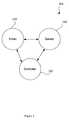
- FIG. 1depicts one implementation of a block diagram of a memory system 100 .
- the memory system 100typically implemented on an integrated circuit chip, includes a re-writable memory array 20 .
- Some inputs to the re-writable memory array 20include an address bus 30 , a control bus 40 and some power supplies 50 .
- Input/output signalsform a data bus 60 .
- the control bus 40includes signals to select the chip, to indicate whether a read or write operation is to be performed, and to enable output buffers within a buffers and drivers block 90 when the chip is in a read operation mode.
- the address bus 30specifies which location within the re-writable memory array 20 is to be accessed.
- Some address lines of the address bus 30go to an X block 70 , which includes a predecoder and an X-decoder to select one of the horizontal array lines addressing the rewritable memory array 20 .
- some address lines of the address bus 30go to a Y block 80 , which includes a predecoder and a Y-decoder to apply appropriate voltages on selected vertical lines.
- 8 vertical linesare selected at once for the case of an 8-bit wide data bus, with each vertical line corresponding to one data line.
- write-datais applied through the data bus 60 to the buffers and drivers 90 , and then to the selected vertical lines, also called bit lines. Meanwhile, the address on the address bus 30 will select which memory cells, located at the intersection of a horizontal line selected by the X-decoder and those vertical lines selected by the Y-decoder, within the re-writable memory array 20 are being written.
- a horizontal line and a number of vertical linesare selected to read each unit of read-data, for example a byte.
- data driversare disabled and sense amplifiers are enabled to detect the state of the selected memory cells with output signals from the selected memory cells, to amplify the output signals and send them to the output buffers which in turn will drive the output pins of the chip.
- the power supply block 50is sometimes added, together with another control block, to generate some of the needed voltages internal to the chip.
- FIG. 2depicts a composite I-V curve 200 of a re-writable conductive memory device with two of its terminal resistance states superimposed.
- R dR i .
- this functionality of R d switchingcan be expressed mathematically as follows:
- R dswitches to R j+1 when V d goes above +VP cj followed by R d switching back to R j when V d drops below ⁇ VN cj
- Re-writable conductive memory device programming cycle timefrom about 0.1 ns to about 100 ⁇ s can be achieved. While a Vd exceeding the threshold voltage would cause a corresponding resistance switching of the re-writable conductive memory device, a higher V d generally, by creating a correspondingly higher electric field within the device, would result in a shorter resistance switching time or equivalently a shorter device programming cycle time. Additionally, it is a good practice to insure that the drive voltage V d is set below a maximum allowable value V max above which unselected re-writable conductive memory device memory cells on a selected line within the memory array could be disturbed due to a parasitic coupling effect.
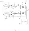
- the present inventionproposes an adaptive programming technique for the re-writable conductive memory device.
- the adaptive programming circuit 300includes a coupled detector 310 , controller 320 and driver 330 .
- the detector 310being coupled to a re-writable conductive memory device, functions to detect R d and to output an indicating signal identifying an R j within the multi-level resistance set (R 1 , R 2 , . . . , R M ) that R d corresponds to.
- the way to decide an R j within the multi-level resistance set that R d corresponds tois simply to determine, in a domain of resistance value of R d , its closest neighbor out of the multi-level resistance set (R 1 , R 2 , . . . , R M ).
- the controller 320being coupled to the detector 310 , functions to detect a write command with write-data and the indicating signal and to generate an activating signal indicating either an activated or a deactivated state.
- the driver 330being coupled to the re-writable conductive memory device and the controller 320 , functions to drive, only while the activating signal is in the activated state, the re-writable conductive memory device to effect a desired switching of R d among the multi-level resistance set.
- the controller 320can further include activating logic functions as follows:
- (b1)a non-correspondence between the indicating signal and the write-data sets the activating signal to an activated state while continuing function (b) thus causing the driver 330 to drive the re-writable conductive memory device to effect a desired switching of R d among the multi-level resistance set; or
- logic element (b2) abovein addition to completing the adaptive aspect of the adaptive programming circuit 300 , also functions to avoid a redundant programming cycle where R d already corresponds to the write-data before the programming cycle. Repetitive redundant programming cycles can potentially cause a shortening of the re-writable conductive memory device operating life.
- the controller 320can further include a pre-determined maximum allowable programming time T max and a timer tracking an elapsed time T Ip of the programming cycle from the moment of presence of the write command.
- LFSLogic Fault Signal
- the activating logicfurther includes the following changes:
- logic element (a)includes an additional, unconditional initialization of LFS to 0.
- logic element (b1)is replaced with the following two logic elements:
- the detector 310further selects an equivalent-reference signal set (REF 1 , REF 2 , . . . , REF M ) depending upon the write data.
- a base reference signalwill typically be an input to the memory system 100 , or derived from resistive circuitry within the memory system 100 .
- the detector 310compares Se q with an appropriate reference signal from the equivalent-reference signal set (REF 1 , REF 2 , . . . , REF M ).
- the driver 330is a switchable, by the activating signal, voltage source with an output voltage V cs
- V csis a constant voltage
- its magnitudemust exceed each respective threshold voltage VP cj and VN cj to effect a desired switching of R d among the multi-level resistance set.
- V dgenerally results in a shorter device programming cycle time
- the V cscan be set as a time-varying voltage ramp of increasing magnitude so as to exceed each respective VP cj and VN cj within a pre-determined time interval to shorten the programming cycle time.
- the initial value of the time-varying voltage rampcan be set at or above a corresponding threshold voltage (VP cj or VN cj ) of the re-writable conductive memory device to further shorten the programming cycle time.
- the driver 330is a switchable, by the activating signal, current source with an output current I cs
- the output current I csis a constant current, of course, its magnitude must cause the corresponding V d to exceed each respective threshold voltage VP cj and VN cj to effect a desired switching of R d among the multi-level resistance set.
- the I cscan be set as a time-varying current ramp of increasing magnitude so as to cause the corresponding V d to exceed each respective VP cj and VN cj within a pre-determined time interval to shorten the programming cycle time.
- the initial value of the time-varying current rampcan be set to cause the corresponding V d to be at or above a corresponding threshold voltage (VP cj or VN cj ) of the re-writable conductive memory device to further shorten the programming cycle time.
- the present inventionis equally applicable to a method of programming the re-writable conductive memory device with a sequence of steps logically corresponding to the above attributes of the adaptive programming circuit. It should also be clear that, except for insuring that V d stays below each respective VP cj and VN cj to avoid the switching of R d , essentially the same adaptive programming circuit can be adapted to effect a read operation outputting an indicating signal identifying an R j that R d corresponds to upon detection of a read-command. Additional, even more detailed embodiments of the detector 310 , the controller 320 and the driver 330 will be presently illustrated graphically.
- FIG. 4Adepicts a first more detailed embodiment of the adaptive programming circuit 300 using a comparator.
- the equivalent-reference signal set selectorincludes a reference driver 400 working in conjunction with a reference data source 410 to provide an equivalent-reference signal REF 1 at node B of a comparator 420 .
- the driver 330includes a program supply 440 and a data driver 450 .
- the program supply 440outputs, inter alia, write-data.
- the data driver 450is a voltage source with an output voltage V cs for effecting an actual programming of the re-writable conductive memory device, located within a re-writable memory array 20 , according to the write-data.
- this particular embodimentessentially employs a current comparison technique and the output of the comparator 420 is logically the indicating signal identifying an R j within the multi-level resistance set (R 1 , R 2 ) that R d corresponds to.
- the controller 320in this case a single feedback signal path, functions to either activate or deactivate the data driver 450 depending upon the correspondence, or not, between the indicating signal and the write-data.
- the current comparison techniqueis further illustrated with a numerical example.
- the selected re-writable conductive memory device to be programmedis in the low resistive state with R d corresponds to R 1 .
- the comparator 420includes a reference current set at 20 ⁇ A, a similar load circuit for the reference current and the selected memory device and a voltage comparator.
- the load circuitsare basically resistor networks connected to the voltage source V CS . As the reference current is 20 ⁇ A and the selected memory device current is 40 ⁇ A, the voltage on node A will be lower than that on node B causing the output of the voltage comparator to be high.
- the comparatorcould be connected with a different polarity of input so that its output would be low. But this would not change the nature of this invention.
- the write voltage V wtstarts to switch the resistance of the selected memory device, its current I d decreases from 40 ⁇ A until it reaches the reference current of 20 82 A. At this point node A voltage equals node B voltage.
- node A voltagebecomes higher than node B voltage that causes the voltage comparator to trip into a state of low output voltage.
- the voltage comparator outputcan be used to deactivate the data driver 450 thus turning off the write voltage V wt applied to the selected memory device.
- the programming voltage pulsedoes not have to be a square pulse of constant amplitude.
- a further improvementwould be to use a ramp on the programming voltage, starting at a low initial voltage value and increasing with time.
- the initial voltagecan start somewhere at or above the read voltage and can go as high as the circuitry allows.
- For a cross point arraythat means the voltage should not disturb unselected memory devices on the selected array lines.
- This techniquecombined with the comparison technique, would insure that memory devices with a fast programming cycle time get programmed quickly at a relatively low voltage.
- memory devices with a slow programming cycle timecan be programmed faster than if a constant voltage was applied as a write voltage.
- a memory devicemay never program under a normal constant voltage drive.
- increasing the write voltageit is now possible to program this memory device.
- FIG. 4Bdepicts a second more detailed embodiment of the adaptive programming circuit 300 using a comparator.
- the equivalent-reference signal set selectorincludes a reference data source 510 providing an equivalent-reference signal REF 1 at node B of a comparator 420 .
- the driver 330includes a program supply 440 and a data driver with voltage detector 520 outputting a detected re-writable conductive memory device voltage V d at node A.
- the program supply 440outputs, inter alias, write-data.
- the data driver with voltage detector 520includes a current source with an output current I cs for effecting an actual programming of the re-writable conductive memory device, located within a re-writable memory array 20 , according to the write-data.
- this particular embodimentessentially employs a voltage comparison technique and the output of the comparator 420 is logically the indicating signal identifying an R j within the multi-level resistance set (R 1 , R 2 ) that R d corresponds to.
- the controller 320in this case a single feedback signal path, functions to either activate or deactivate the data driver with voltage detector 520 depending upon the correspondence, or not, between the indicating signal and the write-data.
- FIG. 5depicts a third circuit schematic level embodiment of the adaptive programming circuit 300 with a bipolar voltage drive, a current comparison circuitry and an activating logic.
- This circuit schematicuses 2 references so that the programmed resistance states R 1 and R 2 are separated by a pre-determined margin.
- R 1 ⁇ R 2a bipolar voltage drive with at least a range of ( ⁇ VN c1 , +VP c1 ) is required.
- the adaptive programming circuit 300includes an upper half circuitry to provide the required positive voltage drive and a lower half circuitry, being essentially a mirror image of the upper half circuitry, to provide the required negative voltage drive.
- the upper half circuitryis also called positive drive circuitry and the lower half circuitry is also called negative drive circuitry. While both the positive drive circuitry and the negative drive circuitry are logically driven by a write command pulse 601 , the positive drive circuitry is only activated with a write-data R 2 signal 602 whereas the negative drive circuitry is only activated with a write-data R 1 signal 603 . In this way, during a programming operation with a positive voltage drive the negative drive circuitry is deactivated in a state of high impedance to avoid any interference with the positive drive circuitry, and vice versa. Focusing on the details of the positive drive circuitry with further reference made to the earlier FIG.
- the controller 320includes an activating logic 600 in turn driving both a device pre-driver 620 and, through an R 2 reference pre-driver 610 , an R 2 reference driver 640 .
- the device pre-driver 620drives a +VP c1 device driver 630 whose output drives a selected re-writable conductive memory device within the re-writable memory array 20 .
- the +VP c1 device driver 630output, through a signal branch at node A, also feeds a negative terminal of a comparator 660 .
- the R 2 reference driver 640 outputin combination with an R 2 reference resistance 650 , establishes an equivalent-reference signal REF 1 at node B that feeds a positive terminal of the comparator 660 . Therefore, with its logic output fed into the activating logic 600 , the comparator 660 would complete the desired function of adaptive programming between Point B and Point C of FIG. 2. Except for working in a domain of negative voltage with a ⁇ VN c1 device driver 680 , by now it should become clear that the negative drive circuitry has a similar circuit topology and functions, in a way similar to the positive drive circuitry above, to accomplish the desired function of adaptive programming between Point D and Point E of FIG. 2. It is also instructional to note that, while FIG.
- the driving circuitcan also be characterized as a hybrid combination of voltage and current source.
- the circuit topology of FIG. 5is used for detecting R d between two levels separated by two reference levels in between to effect a higher detection resolution of R d with a correspondingly higher margin of correct logic decision.
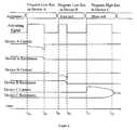
- FIG. 6depicts an exemplary timing diagram of signals and memory device currents during an application of the present invention in a re-writable memory array.
- a first device A within the re-writable memory arrayis programmed with a low resistance state
- a second device Bis programmed with a low resistance state
- a third device Cis programmed with a high resistance state.
- the self-adapting nature of the activating signal having a variable pulse widtheach corresponds to an individual memory device being programmed.
- device Aexhibits a typical programming cycle time of t A2 -t A1
- cell Bexhibits a fast programming cycle time of t B2 -t B1 while cell C exhibits a slow programming cycle time of t C2 -t c1 .
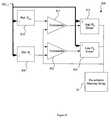
- FIG. 7illustrates another embodiment of the adaptive programming circuit extended to a general case where the re-writable conductive memory device exhibits a multi-level voltage switchable resistance set of more than two resistance levels.
- jthe entire section-j of adaptive programming circuit 720 is selected by a section-j selection signal 722 .
- the section-j selection signal 722Upon selection, the section-j selection signal 722 , for R j programming, activates a reference R j generator 700 to establish an equivalent-reference signal REFj at node B 1 that feeds a first input terminal of a comparator 702 .
- the output of the comparator 702while in an activated state, in turn activates a low R d device driver 704 through a feedback signal path 703 to drive a selected re-writable conductive memory device within the re-writable memory array 20 causing a switching of R d into the R j -state.
- the low R d device driver 704 outputthrough a signal branch at node A, also feeds a second input terminal of the comparator 702 to complete the adaptive programming logic for resistance R j .
- the section-j selection signal 722for R j+1 programming, activates a reference R j+1 generator 710 to establish an equivalent-reference signal REFj+1 at node B 2 that feeds a first input terminal of a comparator 712 .
- FIG. 8depicts a block diagram of an entire adaptive programming circuit 820 with the same functionality as FIG. 7 but a different implementation.
- this approachrequires only 2 comparators 802 and 812 , 2 adjustable references 800 and 810 and 2 adjustable drivers 804 and 814 . This is an advantage where no replication of the section-j circuit would be necessary to implement the programming of the multi-level resistance set (R 1 , R 2 , . . . R M ).
- this front end circuitincludes the device driver 630 , the reference driver 640 , the reference resistance 650 and the comparator 660 .
- an adaptive programming technique for a re-writable conductive memory deviceis proposed to achieve a reliable re-writable conductive memory device programming with a short programming cycle time despite the tolerance of various memory device parameters affecting the programming cycle time.
- the inventionhas been described using exemplary preferred embodiments. However, for those skilled in this field, the preferred embodiments can be easily adapted and modified to suit additional applications without departing from the spirit and scope of this invention.
- the drivercan be generalized into a combination voltage and current drive with an arbitrary output waveform as long as it exceeds the respectively required threshold voltages for programming.
- the scope of the inventionis not limited to the disclosed embodiments. On the contrary, it is intended to cover various modifications and similar arrangements based upon the same operating principle. The scope of the claims, therefore, should be accorded the broadest interpretations so as to encompass all such modifications and similar arrangements.
Landscapes
- Chemical & Material Sciences (AREA)
- Engineering & Computer Science (AREA)
- Materials Engineering (AREA)
- Semiconductor Memories (AREA)
- Read Only Memory (AREA)
Abstract
Description
- This application claims the benefit of U.S. Provisional Application No. 60/422,922, filed Oct. 31, 2002, and the U.S.[0001]
Provisional Application 60/424,083, filed Nov. 5, 2002, all of which are incorporated herein by reference in their entireties and for all purposes. This application is related to the following U.S. Patent Applications: U.S. application Ser. No. 10/360,005, filed Feb. 7, 2003; U.S. application Ser. No. 10/330,512, filed Dec. 26, 2002; application Ser. No. 10/330,153, filed Dec. 26, 2002; application Ser. No. 10/330,964, filed Dec. 26, 2002; application Ser. No. 10/330,170, filed Dec. 26, 2002; application Ser. No. 10/330,900, filed Dec. 26, 2002; application Ser. No. 10/330,150, filed Dec. 26, 2002; application Ser. No. 10/330,965, filed Dec. 26, 2002; application Ser. No. 10/249,846, filed May 12, 2003; application Ser. No. 10/249,848, filed May 12, 2003; application Ser. No. 10/612,733, filed Jul. 1, 2003; application Ser. No. 10/613,099, filed Jul. 1, 2003; application Ser. No. 10/612,191, filed Jul. 1, 2003; application Ser. No. 10/612,263, filed Jul. 1, 2003; application Ser. No. 10/612,776, filed Jul. 1, 2003; application Ser. No. 10/604,556, filed Jul. 30, 2003; application Ser. No. 10/604,606, filed Aug. 4, 2003; and application Ser. No. 10/634,636, filed Aug. 4, 2003. All of the above applications are hereby incorporated herein by reference in their entireties and for all purposes. - 1. Field of the Invention[0002]
- This invention concerns the general field of memory devices. More specifically, the present invention is directed to write circuitry.[0003]
- 2. Description of the Related Art[0004]
- A random access memory (“RAM”) type of memory is typically associated with the main memory available to computer programs and similar devices. RAM memory is often contrasted with a read-only memory (“ROM”) type of memory, which is typically associated with a special memory that is either not changed, or changed relatively infrequently. RAM mostly includes SRAM and DRAM. ROM mostly includes Flash memory, EPROM, OTP, EEPROM, PROM and ROM. Some devices such as NovRAM and Battery powered SRAM are hybrid devices using more than one technology.[0005]
- Although SRAM, with very fast access times, is the memory of choice for computer applications, its volatility, large size and stand-by current limit the total size and applications of the memory. Non-volatile memories such as Flash memory are slower to program, and in some cases must erase a large block of memory before being reprogrammed. DRAM has the smallest cell size, but necessitates a complex refresh algorithm, and is volatile. For new applications, away from PC applications and into portable applications such as cell phones, personal digital assistants (PDA), digital cameras, camcorders, removable “key-chain” or “USB” disks, the key issues are nonvolatility and low power consumption.[0006]
- Regardless of how the memory is used, RAM and ROM overlap in many respects. Both types of memory can allow random access reads. Both types of memory can be relatively fast or relatively slow. Although all ROMs are non-volatile, so are some RAMs. Although most ROMs cannot change their data once programmed, some ROMs can be re-programmed. The only consistent difference between RAM and ROM is that ROM is always non-volatile and RAM is always re-writable.[0007]
- The ROMs that are capable of modifying their data typically require long write cycles that erase entire blocks of data prior to new data being written. For example, UV light might be applied to an entire memory block in order to “repair” fused connections so that the block can be re-written with new data. RAM, on the other hand, can read or write to a randomly accessed byte of memory, typically performing either operation in a standard cycle.[0008]
- Conventional nonvolatile RAM and ROM requires three terminal MOSFET-based devices. The layout of such devices are not ideal, usually requiring feature sizes of at least 8f2 for each memory cell, where f is the minimum feature size.[0009]
- However, not all memory elements require three terminals. Certain conductive metal oxides (CMOs), for example, can retain a resistive state after being exposed to an electronic pulse, which can be generated from two terminals. U.S. Pat. No. 6,204,139, issued Mar. 20, 2001, to Liu et al., incorporated herein by reference for all purposes, describes some perovskite materials that exhibit such characteristics. The perovskite materials are also described by the same researchers in “Electric-pulse-induced reversible resistance change effect in magnetoresistive films,” Applied Physics Letters, Vol. 76, No. 19, 8 May 2000, and “A New Concept for Non-Volatile Memory: The Electric-Pulse Induced Resistive Change Effect in Colossal Magnetoresistive Thin Films,” in materials for the 2001 Non-Volatile Memory Technology Symposium, all of which are hereby incorporated by reference for all purposes.[0010]
- Similarly, the IBM Zurich Research Center has also published three technical papers that also discuss the use of metal oxide material for memory applications: “Reproducible switching effect in thin oxide films for memory applications,” Applied Physics Letters, Vol. 77, No. 1, 3 Jul. 2000, “Current-driven insulator-conductor transition and nonvolatile memory in chromium-doped SrTiO3 single crystals,” Applied Physics Letters, Vol. 78, No. 23, 4 Jun. 2001, and “Electric current distribution across a metal-insulator-metal structure during bistable switching,” Journal of Applied Physics, Vol. 90, No. 6, 15 Sep. 2001, all of which are hereby incorporated by reference for all purposes.[0011]
- Similarly, magnetic RAM (MRAM) requires only two terminals to deliver a magnetic field to the memory element. Other two terminal devices include Ovonic Unified Memory (OUM), which uses chalcogenic layers of material, and various types of ferroelectric memory. With only two terminals, it has been theorized that memory can be arranged in a cross point architecture.[0012]
- However, mere recognition that a two terminal memory element is theoretically capable of being placed in a cross point array does not solve many of the non-trivial problems associated with actually using such a device.[0013]
- For example, as memory is scaled, bit-to-bit variations increase. The size variations of critical layers affect cells that are at minimum dimensions, i.e., at the limit of the lithography capabilities. The variations may results in memory bits with different programming time, and possibly different write thresholds.[0014]
- The standard way to deal with program time difference, as used with EPROM and Flash memories, consists of an algorithm that first writes data by applying an appropriate combination of voltages or current to the selected cells, then verifies data by comparing the data read from the selected cells to the data expected to be programmed, and then, if the data is not properly programmed, write the data again. The process is repeated until the data is correct. If the data does not verify properly after a predetermined number of retries, the memory issues a fail diagnostic.[0015]
- The problem with the above approach is that it is slow, as the memory circuit has to switch back and forth numerous times between read and write modes. Hence, the present invention is directed to electronic systems interfacing with the re-writable conductive memory device, inter alias, to circumvent this problem.[0016]
- The present invention provides a program circuit that can be used to program a selected memory cell. Memory cells are selected out of a memory array in order to write a specific value to a memory device. Each memory cell has a resistance that is capable of representing stored information. The program circuit receives a selected cell input from the selected memory cell and a first reference input, which are used by a comparator. The comparator is capable of producing a first comparator output that is a function of the selected cell input and the first reference input. In some aspects of the invention, the comparator output causes the program circuit to cease programming when the selected cell input equals the first reference input.[0017]
- In another aspect of the invention, an adaptive programming circuit includes a detector, a controller and a driver. The detector detects the resistance of a memory device, R[0018]d. The controller is coupled to the detector and both receive a write command and, based upon the detector's output, the controller generates an activating signal indicating either an activated or a deactivated state. When the activating signal is in the activated state, the driver drives the re-writable conductive memory device such that the resistance of the conductive memory device is modified to a target resistance, Rt, whereby the Rtis already equal to Rdwhen the activating signal is in the deactivated state while the programming circuit is enabled.
- In yet another aspect of the invention, a self terminating programming process for programming a voltage switchable re-writable conductive memory device of resistance R[0019]d, is disclosed. First, a write command for a target resistance Rtis received. Then, a reference current is selected, the selection being dependent upon Rt. Also, a memory cell current is detected, the memory cell current being based upon Rd. The selected reference current is then compared with the memory cell current. A write voltage is then applied across the memory cell for as long as the comparison indicates that Rtis not equal to Rd. Once Rtis equal to Rdthe programming cycle is terminated.
- In yet another aspect of the invention, a program circuit for a programming a selected cell to a desired resistive state receives a first reference input, a second reference input, and a selected cell input. The program circuit includes a first comparator, a second comparator, a first driver and a second driver. The first driver's activation is at least partially dependent upon the first comparator output, which is a function of the first reference input and the selected cell input. Similarly, the second driver's activation is at least partially dependent upon the second comparator output, which is a function of the second reference input and the selected cell input.[0020]
- It yet another aspect of the invention, a program circuit for a programming a selected cell to a desired resistive state receives a reference level and a selected cell level. The program circuit includes a comparator, a first driver, and a second driver. The first driver can provide a voltage capable of increasing the resistance of the selected cell and the second driver can provide a voltage capable of decreasing the resistance of the selected cell. Which of the drivers is activated is dependent upon the comparator output and the desired resistive state.[0021]
- The current invention will be better understood and the nature of the invention set forth above will become apparent when consideration is given to the following detailed description of the preferred embodiments. For clarity of explanation, the detailed description further makes reference to the attached drawings herein:[0022]
- FIG. 1 depicts a block diagram of a re-writable memory array;[0023]
- FIG. 2 depicts a composite current vs. voltage characteristics of a re-writable conductive memory device with two of its terminal resistance states superimposed;[0024]
- FIG. 3 depicts a high-level conceptual diagram of an adaptive programming circuit of the present invention;[0025]
- FIG. 4A depicts a first more detailed embodiment of the adaptive programming circuit using a comparator;[0026]
- FIG. 4B depicts a second more detailed embodiment of the adaptive programming circuit using a comparator;[0027]
- FIG. 5 depicts a third circuit schematic level embodiment of the adaptive programming circuit with a bipolar voltage drive, a current comparison circuitry and an activating logic;[0028]
- FIG. 6 depicts an exemplary timing diagram of signals and device currents during an application of the present invention in a re-writable memory array; and[0029]
- FIG. 7 illustrates another embodiment of the adaptive programming circuit extended to a general case where the re-writable conductive memory device exhibits a multi-level voltage switchable resistance set of more than two resistance levels.[0030]
- FIG. 8 illustrates yet another embodiment of the adaptive programming circuit extended to a general case where the re-writable conductive memory device exhibits a multi-level voltage switchable resistance set of more than two resistance levels.[0031]
- It is to be understood that, in the drawings, like reference numerals designate like structural elements. Also, it should be understood that the depictions in the figures are not necessarily to scale.[0032]
- Glossary[0033]
- As used in the present specification, the following words and phrases are generally intended to have the meanings as set forth below, except to the extent that the context in which they are used indicates otherwise. The following abbreviations and terms have the indicated meanings throughout:[0034]
- The term “array” refers to a plurality of objects arranged in a regular pattern.[0035]
- The term “CMO” refers to a conductive metal oxide[0036]
- The term “cross point memory array” refers to an array with two sets of generally perpendicular lines with memory cells placed at the intersections between the sets of lines[0037]
- The term “Memory Cell” refers to a spatially repeatable set of devices each storing a unit of addressable information, for example one bit[0038]
- The term “Memory Material” refers to a material that is capable of storing information[0039]
- The term “Memory Plug” refers to various layers of materials arranged between conductive lines and including at least a memory material and typically including a top electrode and a bottom electrode[0040]
- In the following detailed description of the present invention, numerous specific details are set forth in order to provide a thorough understanding of the present invention. However, it will become obvious to those skilled in the art that the present invention may be practiced without these specific details. In other instances, well-known methods, procedures, materials, components and circuitry have not been described in detail to avoid unnecessary obscuring aspects of the present invention. The detailed description is presented largely in terms of simplified semiconductor device terminal I-V characteristics, circuit block diagrams, circuit schematics and timing diagrams. These descriptions and representations are the means used by those experienced or skilled in the art to concisely and most effectively convey the substance of their work to others skilled in the art.[0041]
- FIG. 1 depicts one implementation of a block diagram of a[0042]
memory system 100. Thememory system 100, typically implemented on an integrated circuit chip, includes are-writable memory array 20. Some inputs to there-writable memory array 20 include anaddress bus 30, acontrol bus 40 and some power supplies50. Input/output signals form adata bus 60. Thecontrol bus 40 includes signals to select the chip, to indicate whether a read or write operation is to be performed, and to enable output buffers within a buffers and drivers block90 when the chip is in a read operation mode. Theaddress bus 30 specifies which location within there-writable memory array 20 is to be accessed. Some address lines of theaddress bus 30 go to anX block 70, which includes a predecoder and an X-decoder to select one of the horizontal array lines addressing therewritable memory array 20. Likewise, some address lines of theaddress bus 30 go to a Y block80, which includes a predecoder and a Y-decoder to apply appropriate voltages on selected vertical lines. Typically 8 vertical lines are selected at once for the case of an 8-bit wide data bus, with each vertical line corresponding to one data line. - During a write operation (following a write command with write-data) write-data is applied through the[0043]
data bus 60 to the buffers anddrivers 90, and then to the selected vertical lines, also called bit lines. Meanwhile, the address on theaddress bus 30 will select which memory cells, located at the intersection of a horizontal line selected by the X-decoder and those vertical lines selected by the Y-decoder, within there-writable memory array 20 are being written. - Similarly, during a read operation, a horizontal line and a number of vertical lines are selected to read each unit of read-data, for example a byte. Meanwhile, within the buffers and drivers block[0044]90, data drivers are disabled and sense amplifiers are enabled to detect the state of the selected memory cells with output signals from the selected memory cells, to amplify the output signals and send them to the output buffers which in turn will drive the output pins of the chip. The power supply block50 is sometimes added, together with another control block, to generate some of the needed voltages internal to the chip.
- While the above describes the essence of the operation of a memory system, in practice, many other circuits may be added to further enhance the memory functionality, manufacturing yield, testability and other features. However, these other circuits are not necessary for the understanding of the present invention to be presently described.[0045]
- The[0046]
re-writable memory array 20 itself is described in U.S. application Ser. No. 10/604,606 filed Aug. 4, 2003 already incorporated by reference. - The functionality of the re-writable conductive memory device, with a voltage switchable resistance R[0047]d, is illustrated in FIG. 2 that depicts a composite
I-V curve 200 of a re-writable conductive memory device with two of its terminal resistance states superimposed. It is remarked that, in general, the resistance Rdis voltage switchable within a multi-level resistance set Rjwhere j=(1,2, . . . ,M), with M>=2 and R1<R2< . . . <RM, and each value of Rjthus representing a correspondingly stored data. Starting with Point A of drive voltage Vd=0 thus drive current Id=0, within the region between Point A and Point B and characterized by: - 0<=Vd<=+VPci
- R[0048]d=Ri. However, once a threshold voltage +VPciwith an accompanying critical electric field strength is exceeded, for a duration of resistance switching time, within the re-writable conductive memory device the current flow changes to a generally lower value. This is indicated by Point C with a dashed pointing arrow. Now if Vdis taken to a value that is more negative than −VNcifor a duration of resistance switching time, then the
composite I-V curve 200 switches back from Point D to Point E as indicated by another dashed pointing arrow. Thus, in general, this functionality of Rdswitching can be expressed mathematically as follows: - Rd=Rjwhen −VNcj<=Vd<=+VPcj; and
- R[0049]dswitches to Rj+1when Vdgoes above +VPcjfollowed by Rdswitching back to Rjwhen Vddrops below −VNcj
- where M>=2, j=(1, 2, . . . , M−1) and each of VP[0050]cjand VNcjis a pre-determined threshold voltage magnitude.
- Re-writable conductive memory device programming cycle time from about 0.1 ns to about 100 μs can be achieved. While a Vd exceeding the threshold voltage would cause a corresponding resistance switching of the re-writable conductive memory device, a higher V[0051]dgenerally, by creating a correspondingly higher electric field within the device, would result in a shorter resistance switching time or equivalently a shorter device programming cycle time. Additionally, it is a good practice to insure that the drive voltage Vdis set below a maximum allowable value Vmaxabove which unselected re-writable conductive memory device memory cells on a selected line within the memory array could be disturbed due to a parasitic coupling effect. Likewise, it is also a good practice to insure that the drive current Idis set below a maximum allowable value Imaxabove which unselected re-writable conductive memory device memory cells on a selected line within the memory array could be disturbed due to the same parasitic coupling effect. It should be further noticed that although FIG. 2 shows linear IV characteristics, it is also possible for the memory cell to exhibit non-linear characteristics, as further described in U.S. application Ser. No. 10/604,556, already incorporated herein by reference for all purposes. Therefore, the terms “resistive memory” and “resistive device” also apply to memories and devices showing non-linear characteristics, and can also be referred to respectively as “conductive memory” and “conductive device”.
- As alluded to before, scaling down the re-writable conductive memory device size within a re-writable memory array for high memory density will, especially at the limit of lithographic capabilities, increase bit-to-bit tolerance of numerous device geometric, material and electrical parameters. This may result in memory cells exhibiting different programming cycle time and possibly different threshold voltage as well. To insure a reliable re-writable conductive memory device programming with a short programming cycle time despite these device parameter tolerances, the present invention proposes an adaptive programming technique for the re-writable conductive memory device.[0052]
- A high-level conceptual diagram of an adaptive programming circuit of the present invention is depicted in FIG. 3. The[0053]
adaptive programming circuit 300 includes a coupleddetector 310,controller 320 anddriver 330. Thedetector 310, being coupled to a re-writable conductive memory device, functions to detect Rdand to output an indicating signal identifying an Rjwithin the multi-level resistance set (R1, R2, . . . , RM) that Rdcorresponds to. For those skilled in the art, the way to decide an Rjwithin the multi-level resistance set that Rdcorresponds to is simply to determine, in a domain of resistance value of Rd, its closest neighbor out of the multi-level resistance set (R1, R2, . . . , RM). Thecontroller 320, being coupled to thedetector 310, functions to detect a write command with write-data and the indicating signal and to generate an activating signal indicating either an activated or a deactivated state. Thedriver 330, being coupled to the re-writable conductive memory device and thecontroller 320, functions to drive, only while the activating signal is in the activated state, the re-writable conductive memory device to effect a desired switching of Rdamong the multi-level resistance set. Thecontroller 320 can further include activating logic functions as follows: - (a) an absence of the write command (or the presence of a read command) sets the activating signal to a deactivated state thus insuring that the re-writable conductive memory device is not driven by the[0054]
driver 330. - (b) a presence of the write command activates a comparison of the indicating signal with the write-data; and[0055]
- (b1) a non-correspondence between the indicating signal and the write-data sets the activating signal to an activated state while continuing function (b) thus causing the[0056]
driver 330 to drive the re-writable conductive memory device to effect a desired switching of Rdamong the multi-level resistance set; or - (b2) a correspondence between the indicating signal and the write-data sets the activating signal to a deactivated state and terminates the programming cycle.[0057]
- Notice that logic element (b2) above, in addition to completing the adaptive aspect of the[0058]
adaptive programming circuit 300, also functions to avoid a redundant programming cycle where Rdalready corresponds to the write-data before the programming cycle. Repetitive redundant programming cycles can potentially cause a shortening of the re-writable conductive memory device operating life. - To deal with re-writable conductive memory devices that either are unreasonably hard to program or would require an unreasonably long programming cycle time or simply have failed in time, the[0059]
controller 320 can further include a pre-determined maximum allowable programming time Tmaxand a timer tracking an elapsed time TIpof the programming cycle from the moment of presence of the write command. Correspondingly, the above activating logic is first modified to include a Logic Fault Signal (LFS) with, for example, LFS=1 means a fault condition and LFS=0 means a no-fault condition. Secondly, the activating logic adds, to function (b), a logic that sets LFS=1 if TIp>Tmax. Thirdly, the activating logic further includes the following changes: - 1. logic element (a) includes an additional, unconditional initialization of LFS to 0.[0060]
- 2. logic element (b1) is replaced with the following two logic elements:[0061]
- (b11) a non-correspondence between the indicating signal and the write-data, while LFS=0, sets the activating signal to an activated state while continuing function (b) thus causing the[0062]
driver 330 to drive the re-writable conductive memory device to effect a desired switching of Rdamong the multi-level resistance set; or - (b12) a non-correspondence between the indicating signal and the write-data, but LFS=1, sets the activating signal to a deactivated state and terminates the programming cycle.[0063]
- For simplicity of implementation in practice, to effect the function of detecting R[0064]dand outputting an indicating signal identifying an Rjwithin the multi-level resistance set (R1, R2, . . . , RM) that Rdcorresponds to, the
detector 310 includes an equivalent-signal Seqgenerator, whose value corresponds to Rdthrough a pre-determined function Rd=f (Seq) follows: - R1=f(Seq1), R2=f(Seq2), . . . and RM=f (SeqM) (1)
- The[0065]
detector 310 further selects an equivalent-reference signal set (REF1, REF2, . . . , REFM) depending upon the write data. A base reference signal will typically be an input to thememory system 100, or derived from resistive circuitry within thememory system 100 . Additionally, thedetector 310 compares Seqwith an appropriate reference signal from the equivalent-reference signal set (REF1, REF2, . . . , REFM). - For one example, the[0066]
driver 330 is a switchable, by the activating signal, voltage source with an output voltage Vcs, the equivalent-signal Seqgenerator can be a current detector, coupled to the re-writable conductive memory device, providing the re-writable conductive memory device current Idas the equivalent-signal Seq. That is Seq=Id. Consequently, the pre-determined function Rd=f(Seq) can simply be Rd=Vcs/Idby Ohm's law. Where the output voltage Vcsis a constant voltage, of course, its magnitude must exceed each respective threshold voltage VPcjand VNcjto effect a desired switching of Rdamong the multi-level resistance set. As a higher Vdgenerally results in a shorter device programming cycle time, for those re-writable conductive memory devices having high threshold voltages VPcjand VNcjthe Vcscan be set as a time-varying voltage ramp of increasing magnitude so as to exceed each respective VPcjand VNcjwithin a pre-determined time interval to shorten the programming cycle time. Of course, the initial value of the time-varying voltage ramp can be set at or above a corresponding threshold voltage (VPcjor VNcj) of the re-writable conductive memory device to further shorten the programming cycle time. - For another example, the[0067]
driver 330 is a switchable, by the activating signal, current source with an output current Icsthe equivalent-signal Seqgenerator can be a voltage detector, coupled to the re-writable conductive memory device, providing the re-writable conductive memory device voltage Vdas the equivalent-signal Seq. That is Seq=Vd. Consequently, the pre-determined function Rd=f(Seq) can be Rd=Vd/Ics, also by Ohm's law. Where the output current Icsis a constant current, of course, its magnitude must cause the corresponding Vdto exceed each respective threshold voltage VPcjand VNcjto effect a desired switching of Rdamong the multi-level resistance set. As a higher Vdgenerally results in a shorter device programming cycle time, for those re-writable conductive memory devices having high threshold voltages VPcjand VNcj, the Icscan be set as a time-varying current ramp of increasing magnitude so as to cause the corresponding Vdto exceed each respective VPcjand VNcjwithin a pre-determined time interval to shorten the programming cycle time. Of course, the initial value of the time-varying current ramp can be set to cause the corresponding Vdto be at or above a corresponding threshold voltage (VPcjor VNcj) of the re-writable conductive memory device to further shorten the programming cycle time. - By now it should become clear that, in addition to being an adaptive programming circuit, the present invention is equally applicable to a method of programming the re-writable conductive memory device with a sequence of steps logically corresponding to the above attributes of the adaptive programming circuit. It should also be clear that, except for insuring that V[0068]dstays below each respective VPcjand VNcjto avoid the switching of Rd, essentially the same adaptive programming circuit can be adapted to effect a read operation outputting an indicating signal identifying an Rjthat Rdcorresponds to upon detection of a read-command. Additional, even more detailed embodiments of the
detector 310, thecontroller 320 and thedriver 330 will be presently illustrated graphically. - FIG. 4A depicts a first more detailed embodiment of the[0069]
adaptive programming circuit 300 using a comparator. In this case the multi-level resistance set Rjconsists of only two distinct resistance levels R1<R2, that is M=2. As part of thedetector 310, the equivalent-reference signal set selector includes areference driver 400 working in conjunction with areference data source 410 to provide an equivalent-reference signal REF1at node B of acomparator 420. Thedriver 330 includes aprogram supply 440 and adata driver 450. Theprogram supply 440 outputs, inter alia, write-data. Thedata driver 450 is a voltage source with an output voltage Vcsfor effecting an actual programming of the re-writable conductive memory device, located within are-writable memory array 20, according to the write-data. The equivalent-signal Seqgenerator is acurrent detector 430, coupled to the re-writable conductive memory device, providing the equivalent-signal Seq=Id, at node A. Consequently, the pre-determined function Rd=f (Seq) is Rd=Vcs/Id. Hence, this particular embodiment essentially employs a current comparison technique and the output of thecomparator 420 is logically the indicating signal identifying an Rjwithin the multi-level resistance set (R1, R2) that Rdcorresponds to. Thecontroller 320, in this case a single feedback signal path, functions to either activate or deactivate thedata driver 450 depending upon the correspondence, or not, between the indicating signal and the write-data. - The current comparison technique is further illustrated with a numerical example. Here the selected re-writable conductive memory device to be programmed is in the low resistive state with R[0070]dcorresponds to R1. When a write voltage Vwtis initially applied to the cell Id=40 μA before any resistance switching takes place The
comparator 420 includes a reference current set at 20 μA, a similar load circuit for the reference current and the selected memory device and a voltage comparator. The load circuits are basically resistor networks connected to the voltage source VCS. As the reference current is 20 μA and the selected memory device current is 40 μA, the voltage on node A will be lower than that on node B causing the output of the voltage comparator to be high. Notice that, instead, the comparator could be connected with a different polarity of input so that its output would be low. But this would not change the nature of this invention. In time, as the write voltage Vwtstarts to switch the resistance of the selected memory device, its current Iddecreases from 40 μA until it reaches the reference current of 2082 A. At this point node A voltage equals node B voltage. As the programming of the selected memory device progresses further, node A voltage becomes higher than node B voltage that causes the voltage comparator to trip into a state of low output voltage. Hence, the voltage comparator output can be used to deactivate thedata driver 450 thus turning off the write voltage Vwtapplied to the selected memory device. - On the other hand, if the selected memory device to be programmed is already in the high resistive state with R[0071]dcorresponds to R2thus, for example, Id=15 μA at start of the programming operation, the comparator output will stay low and the data driver will stay deactivated.
- Notice that the above circuit needs to be properly initialized. If, at the beginning of the write cycle, the node A voltage starts at a value higher than the node B voltage, the output of the voltage comparator is low thus the[0072]
data driver 450 stays disabled. The consequence is that the program operation would never start. To avoid this problem a discharge circuit and an initialization pulse can be used to force node A voltage low at the beginning of each program operation. - It is further remarked that, while only one reference current is needed in the above example for minimum functionality, this would not provide a more precise resolution of the actual resistance values R[0073]1and R2. Thus, if so desired, additional reference current levels can be included in the adaptive programming circuitry to further improve the detection margin of the various resistance levels.
- As already remarked before, the programming voltage pulse does not have to be a square pulse of constant amplitude. A further improvement would be to use a ramp on the programming voltage, starting at a low initial voltage value and increasing with time. The initial voltage can start somewhere at or above the read voltage and can go as high as the circuitry allows. For a cross point array, that means the voltage should not disturb unselected memory devices on the selected array lines. This technique, combined with the comparison technique, would insure that memory devices with a fast programming cycle time get programmed quickly at a relatively low voltage. On the other hand, memory devices with a slow programming cycle time can be programmed faster than if a constant voltage was applied as a write voltage. Furthermore, if a memory device has a very high write threshold voltage it may never program under a normal constant voltage drive. Here, by increasing the write voltage it is now possible to program this memory device. However, it may not be desirable to program all the memory devices of the array with the increased write voltage as this could prematurely wear out or even damage those memory devices easily programmable at lower voltage levels.[0074]
- FIG. 4B depicts a second more detailed embodiment of the[0075]
adaptive programming circuit 300 using a comparator. The multi-level resistance set Rjstill consists of only two distinct resistance levels R1<R2, that is M=2. As part of thedetector 310, the equivalent-reference signal set selector includes areference data source 510 providing an equivalent-reference signal REF1at node B of acomparator 420. Thedriver 330 includes aprogram supply 440 and a data driver withvoltage detector 520 outputting a detected re-writable conductive memory device voltage Vdat node A. Theprogram supply 440 outputs, inter alias, write-data. The data driver withvoltage detector 520 includes a current source with an output current Icsfor effecting an actual programming of the re-writable conductive memory device, located within are-writable memory array 20, according to the write-data. Thus, the equivalent-signal Seqgenerator is the above voltage detector, coupled to the re-writable conductive memory device, providing the equivalent-signal Seq=Vd, at node A. Hence, this particular embodiment essentially employs a voltage comparison technique and the output of thecomparator 420 is logically the indicating signal identifying an Rjwithin the multi-level resistance set (R1, R2) that Rdcorresponds to. Thecontroller 320, in this case a single feedback signal path, functions to either activate or deactivate the data driver withvoltage detector 520 depending upon the correspondence, or not, between the indicating signal and the write-data. - FIG. 5 depicts a third circuit schematic level embodiment of the[0076]
adaptive programming circuit 300 with a bipolar voltage drive, a current comparison circuitry and an activating logic. This circuit schematic uses 2 references so that the programmed resistance states R1and R2are separated by a pre-determined margin. Referring back to FIG. 2, to effect a reversible switching of Rdbetween R1and R2(R1<R2) a bipolar voltage drive with at least a range of (−VNc1, +VPc1) is required. Correspondingly, theadaptive programming circuit 300 includes an upper half circuitry to provide the required positive voltage drive and a lower half circuitry, being essentially a mirror image of the upper half circuitry, to provide the required negative voltage drive. For convenience, the upper half circuitry is also called positive drive circuitry and the lower half circuitry is also called negative drive circuitry. While both the positive drive circuitry and the negative drive circuitry are logically driven by awrite command pulse 601, the positive drive circuitry is only activated with a write-data R2signal602 whereas the negative drive circuitry is only activated with a write-data R1signal603. In this way, during a programming operation with a positive voltage drive the negative drive circuitry is deactivated in a state of high impedance to avoid any interference with the positive drive circuitry, and vice versa. Focusing on the details of the positive drive circuitry with further reference made to the earlier FIG. 3, thecontroller 320 includes an activatinglogic 600 in turn driving both adevice pre-driver 620 and, through an R2reference pre-driver610, an R2reference driver640. Thedevice pre-driver 620 drives a +VPc1device driver630 whose output drives a selected re-writable conductive memory device within there-writable memory array 20. In parallel, the +VPc1device driver630 output, through a signal branch at node A, also feeds a negative terminal of acomparator 660. The R2reference driver640 output, in combination with an R2reference resistance650, establishes an equivalent-reference signal REF1 at node B that feeds a positive terminal of thecomparator 660. Therefore, with its logic output fed into the activatinglogic 600, thecomparator 660 would complete the desired function of adaptive programming between Point B and Point C of FIG. 2. Except for working in a domain of negative voltage with a −VNc1device driver680, by now it should become clear that the negative drive circuitry has a similar circuit topology and functions, in a way similar to the positive drive circuitry above, to accomplish the desired function of adaptive programming between Point D and Point E of FIG. 2. It is also instructional to note that, while FIG. 5 depicts an embodiment with a bipolar voltage drive, there is nevertheless a typically small drain-to-source voltage drop across the +VPc1device driver630 and the −VNc1device driver680. Furthermore, the drain-to-source voltage drop itself is dependent upon the conductive memory device current Id. Thus, the driving circuit can also be characterized as a hybrid combination of voltage and current source. Lastly, for those skilled in the art, the circuit topology of FIG. 5 is used for detecting Rdbetween two levels separated by two reference levels in between to effect a higher detection resolution of Rdwith a correspondingly higher margin of correct logic decision. - FIG. 6 depicts an exemplary timing diagram of signals and memory device currents during an application of the present invention in a re-writable memory array. In this example, a first device A within the re-writable memory array is programmed with a low resistance state, a second device B is programmed with a low resistance state and a third device C is programmed with a high resistance state. Notice the self-adapting nature of the activating signal having a variable pulse width each corresponds to an individual memory device being programmed. That is, device A exhibits a typical programming cycle time of t[0077]A2-tA1, cell B exhibits a fast programming cycle time of tB2-tB1while cell C exhibits a slow programming cycle time of tC2-tc1.
- FIG. 7 illustrates another embodiment of the adaptive programming circuit extended to a general case where the re-writable conductive memory device exhibits a multi-level voltage switchable resistance set of more than two resistance levels. To avoid unnecessary obscuring aspects of the present invention only section-j of[0078]
adaptive programming circuit 720 is illustrated here where j=(1,2, . . . ,M−1), M>=3 and R1<R2< . . . <RM. However, it should be understood that all other sections are set in parallel, with a common connection at node A, with section-j. First of all, the entire section-j ofadaptive programming circuit 720 is selected by a section-j selection signal 722. Upon selection, the section-j selection signal 722, for Rjprogramming, activates a reference Rjgenerator700 to establish an equivalent-reference signal REFj at node B1 that feeds a first input terminal of acomparator 702. The output of thecomparator 702, while in an activated state, in turn activates a low Rddevice driver704 through afeedback signal path 703 to drive a selected re-writable conductive memory device within there-writable memory array 20 causing a switching of Rdinto the Rj-state. In parallel, the low Rddevice driver704 output, through a signal branch at node A, also feeds a second input terminal of thecomparator 702 to complete the adaptive programming logic for resistance Rj. Similarly, the section-j selection signal 722, for Rj+1programming, activates a reference Rj+1generator710 to establish an equivalent-reference signal REFj+1 at node B2 that feeds a first input terminal of acomparator 712. The output of thecomparator 712, while in an activated state, in turn activates a high Rddevice driver714 through afeedback signal path 713 to drive a selected re-writable conductive memory device within there-writable memory array 20 causing a switching of Rdinto the Rj+1-state. In parallel, the high Rddevice driver714 output, through the signal branch at node A, also feeds a second input terminal of thecomparator 712 to complete the adaptive programming logic for resistance Rj+1. As an alternative embodiment to FIG. 7, FIG. 8 depicts a block diagram of an entireadaptive programming circuit 820 with the same functionality as FIG. 7 but a different implementation. The state-j selection signal 822, which tells the circuit which is the desired state out of M states, and includes typically k lines, so that M=2k, can be applied to the tworeference generators device drivers comparators adjustable references adjustable drivers - Regardless of the detailed description of the various embodiments above, considering the simplicity of implementation, the front end of the circuit schematic as depicted in FIG. 5 is considered to be the best for practicing the present invention. Specifically, this front end circuit includes the[0079]
device driver 630, thereference driver 640, thereference resistance 650 and thecomparator 660. - As described, an adaptive programming technique for a re-writable conductive memory device is proposed to achieve a reliable re-writable conductive memory device programming with a short programming cycle time despite the tolerance of various memory device parameters affecting the programming cycle time. The invention has been described using exemplary preferred embodiments. However, for those skilled in this field, the preferred embodiments can be easily adapted and modified to suit additional applications without departing from the spirit and scope of this invention. For example, the driver can be generalized into a combination voltage and current drive with an arbitrary output waveform as long as it exceeds the respectively required threshold voltages for programming. Thus, it is to be understood that the scope of the invention is not limited to the disclosed embodiments. On the contrary, it is intended to cover various modifications and similar arrangements based upon the same operating principle. The scope of the claims, therefore, should be accorded the broadest interpretations so as to encompass all such modifications and similar arrangements.[0080]
Claims (38)
Priority Applications (2)
| Application Number | Priority Date | Filing Date | Title |
|---|---|---|---|
| US10/680,508US6940744B2 (en) | 2002-10-31 | 2003-10-06 | Adaptive programming technique for a re-writable conductive memory device |
| US11/218,655US7054183B2 (en) | 2002-10-31 | 2005-09-02 | Adaptive programming technique for a re-writable conductive memory device |
Applications Claiming Priority (3)
| Application Number | Priority Date | Filing Date | Title |
|---|---|---|---|
| US42292202P | 2002-10-31 | 2002-10-31 | |
| US42408302P | 2002-11-05 | 2002-11-05 | |
| US10/680,508US6940744B2 (en) | 2002-10-31 | 2003-10-06 | Adaptive programming technique for a re-writable conductive memory device |
Related Child Applications (1)
| Application Number | Title | Priority Date | Filing Date |
|---|---|---|---|
| US11/218,655ContinuationUS7054183B2 (en) | 2002-10-31 | 2005-09-02 | Adaptive programming technique for a re-writable conductive memory device |
Publications (2)
| Publication Number | Publication Date |
|---|---|
| US20040160798A1true US20040160798A1 (en) | 2004-08-19 |
| US6940744B2 US6940744B2 (en) | 2005-09-06 |
Family
ID=32854277
Family Applications (2)
| Application Number | Title | Priority Date | Filing Date |
|---|---|---|---|
| US10/680,508Expired - LifetimeUS6940744B2 (en) | 2002-10-31 | 2003-10-06 | Adaptive programming technique for a re-writable conductive memory device |
| US11/218,655Expired - LifetimeUS7054183B2 (en) | 2002-10-31 | 2005-09-02 | Adaptive programming technique for a re-writable conductive memory device |
Family Applications After (1)
| Application Number | Title | Priority Date | Filing Date |
|---|---|---|---|
| US11/218,655Expired - LifetimeUS7054183B2 (en) | 2002-10-31 | 2005-09-02 | Adaptive programming technique for a re-writable conductive memory device |
Country Status (1)
| Country | Link |
|---|---|
| US (2) | US6940744B2 (en) |
Cited By (27)
| Publication number | Priority date | Publication date | Assignee | Title |
|---|---|---|---|---|
| US20060250836A1 (en)* | 2005-05-09 | 2006-11-09 | Matrix Semiconductor, Inc. | Rewriteable memory cell comprising a diode and a resistance-switching material |
| US20060250837A1 (en)* | 2005-05-09 | 2006-11-09 | Sandisk 3D, Llc | Nonvolatile memory cell comprising a diode and a resistance-switching material |
| US20060273298A1 (en)* | 2005-06-02 | 2006-12-07 | Matrix Semiconductor, Inc. | Rewriteable memory cell comprising a transistor and resistance-switching material in series |
| US20070114508A1 (en)* | 2005-11-23 | 2007-05-24 | Matrix Semiconductor, Inc. | Reversible resistivity-switching metal oxide or nitride layer with added metal |
| US20070114509A1 (en)* | 2005-11-23 | 2007-05-24 | Sandisk 3D Llc | Memory cell comprising nickel-cobalt oxide switching element |
| DE102005061995A1 (en)* | 2005-12-23 | 2007-06-28 | Infineon Technologies Ag | Memory circuit, has discharge circuit formed to make possible discharge current in or from bit circuit to aid recharging of bit circuit, where recharging of bit circuit is caused by changing resistance of resistance memory unit |
| US20070171698A1 (en)* | 2005-12-23 | 2007-07-26 | Heinz Hoenigschmid | Memory circuit including a resistive memory element and method for operating such a memory circuit |
| US20070228414A1 (en)* | 2006-03-31 | 2007-10-04 | Sandisk 3D, Llc | Heterojunction device comprising a semiconductor and a resistivity-switching oxide or nitride |
| US20070236981A1 (en)* | 2006-03-31 | 2007-10-11 | Sandisk 3D, Llc | Multilevel nonvolatile memory cell comprising a resistivity-switching oxide or nitride and an antifuse |
| US20080025080A1 (en)* | 2006-07-27 | 2008-01-31 | Cswitch Corporation | Method and apparatus for programming phase change devices |
| US20080277644A1 (en)* | 2007-05-08 | 2008-11-13 | International Business Machines Corporation | Switch array circuit and system using programmable via structures with phase change materials |
| US20090001344A1 (en)* | 2007-06-29 | 2009-01-01 | April Schricker | Memory cell that employs a selectively grown reversible resistance-switching element and methods of forming the same |
| US20090001343A1 (en)* | 2007-06-29 | 2009-01-01 | April Schricker | Memory cell that employs a selectively deposited reversible resistance-switching element and methods of forming the same |
| US20090001342A1 (en)* | 2007-06-29 | 2009-01-01 | April Schricker | Memory cell that employs a selectively grown reversible resistance-switching element and methods of forming the same |
| US20090001345A1 (en)* | 2007-06-29 | 2009-01-01 | April Schricker | Memory cell that employs a selectively deposited reversible resistance-switching element and methods of forming the same |
| WO2009158673A1 (en)* | 2008-06-27 | 2009-12-30 | Sandisk 3D Llc | Simultaneous write and verify in a non-volatile storage |
| DE102005036555B4 (en)* | 2004-09-02 | 2010-07-01 | Samsung Electronics Co., Ltd., Suwon | Programming programmable resistive memory devices |
| US7829875B2 (en) | 2006-03-31 | 2010-11-09 | Sandisk 3D Llc | Nonvolatile rewritable memory cell comprising a resistivity-switching oxide or nitride and an antifuse |
| US7932548B2 (en) | 2006-07-14 | 2011-04-26 | 4D-S Pty Ltd. | Systems and methods for fabricating self-aligned memory cell |
| US8395199B2 (en) | 2006-03-25 | 2013-03-12 | 4D-S Pty Ltd. | Systems and methods for fabricating self-aligned memory cell |
| US8454810B2 (en) | 2006-07-14 | 2013-06-04 | 4D-S Pty Ltd. | Dual hexagonal shaped plasma source |
| US8711596B2 (en) | 2009-04-20 | 2014-04-29 | Sandisk 3D Llc | Memory system with data line switching scheme |
| US8913413B2 (en) | 2008-08-25 | 2014-12-16 | Sandisk 3D Llc | Memory system with sectional data lines |
| JP2016152060A (en)* | 2015-02-17 | 2016-08-22 | 華邦電子股▲ふん▼有限公司 | Writing and verifying circuit and method for writing and verifying resistive memory thereof |
| DE102006060424B4 (en)* | 2006-01-03 | 2017-04-06 | Polaris Innovations Ltd. | Storage |
| CN111326201A (en)* | 2020-02-19 | 2020-06-23 | 上海集成电路研发中心有限公司 | Self-turn-off circuit and semiconductor memory structure |
| US20220414025A1 (en)* | 2017-09-15 | 2022-12-29 | Mythic, Inc. | System and methods for mixed-signal computing |
Families Citing this family (105)
| Publication number | Priority date | Publication date | Assignee | Title |
|---|---|---|---|---|
| US7038960B2 (en)* | 2002-09-10 | 2006-05-02 | Silicon Storage Technology, Inc. | High speed and high precision sensing for digital multilevel non-volatile memory system |
| US6940744B2 (en)* | 2002-10-31 | 2005-09-06 | Unity Semiconductor Corporation | Adaptive programming technique for a re-writable conductive memory device |
| US6962648B2 (en)* | 2003-09-15 | 2005-11-08 | Global Silicon Net Corp. | Back-biased face target sputtering |
| US7082052B2 (en) | 2004-02-06 | 2006-07-25 | Unity Semiconductor Corporation | Multi-resistive state element with reactive metal |
| US20060171200A1 (en) | 2004-02-06 | 2006-08-03 | Unity Semiconductor Corporation | Memory using mixed valence conductive oxides |
| US20060081467A1 (en)* | 2004-10-15 | 2006-04-20 | Makoto Nagashima | Systems and methods for magnetron deposition |
| US20060081466A1 (en)* | 2004-10-15 | 2006-04-20 | Makoto Nagashima | High uniformity 1-D multiple magnet magnetron source |
| US7425504B2 (en)* | 2004-10-15 | 2008-09-16 | 4D-S Pty Ltd. | Systems and methods for plasma etching |
| US7701834B2 (en)* | 2005-01-18 | 2010-04-20 | Unity Semiconductor Corporation | Movable terminal in a two terminal memory array |
| US7158431B2 (en) | 2005-03-28 | 2007-01-02 | Silicon Storage Technology, Inc. | Single transistor sensing and double transistor sensing for flash memory |
| US8565003B2 (en) | 2011-06-28 | 2013-10-22 | Unity Semiconductor Corporation | Multilayer cross-point memory array having reduced disturb susceptibility |
| US20130082232A1 (en) | 2011-09-30 | 2013-04-04 | Unity Semiconductor Corporation | Multi Layered Conductive Metal Oxide Structures And Methods For Facilitating Enhanced Performance Characteristics Of Two Terminal Memory Cells |
| US8559209B2 (en) | 2011-06-10 | 2013-10-15 | Unity Semiconductor Corporation | Array voltage regulating technique to enable data operations on large cross-point memory arrays with resistive memory elements |
| US8937292B2 (en) | 2011-08-15 | 2015-01-20 | Unity Semiconductor Corporation | Vertical cross point arrays for ultra high density memory applications |
| US8270193B2 (en) | 2010-01-29 | 2012-09-18 | Unity Semiconductor Corporation | Local bit lines and methods of selecting the same to access memory elements in cross-point arrays |
| US7417903B2 (en)* | 2005-09-29 | 2008-08-26 | Hynix Semiconductor Inc. | Core voltage generator and method for generating core voltage in semiconductor memory device |
| US7635855B2 (en) | 2005-11-15 | 2009-12-22 | Macronix International Co., Ltd. | I-shaped phase change memory cell |
| US7786460B2 (en) | 2005-11-15 | 2010-08-31 | Macronix International Co., Ltd. | Phase change memory device and manufacturing method |
| US7449710B2 (en) | 2005-11-21 | 2008-11-11 | Macronix International Co., Ltd. | Vacuum jacket for phase change memory element |
| US7599217B2 (en) | 2005-11-22 | 2009-10-06 | Macronix International Co., Ltd. | Memory cell device and manufacturing method |
| US7688619B2 (en) | 2005-11-28 | 2010-03-30 | Macronix International Co., Ltd. | Phase change memory cell and manufacturing method |
| US7459717B2 (en) | 2005-11-28 | 2008-12-02 | Macronix International Co., Ltd. | Phase change memory cell and manufacturing method |
| US8062833B2 (en) | 2005-12-30 | 2011-11-22 | Macronix International Co., Ltd. | Chalcogenide layer etching method |
| US7560337B2 (en) | 2006-01-09 | 2009-07-14 | Macronix International Co., Ltd. | Programmable resistive RAM and manufacturing method |
| US7741636B2 (en) | 2006-01-09 | 2010-06-22 | Macronix International Co., Ltd. | Programmable resistive RAM and manufacturing method |
| US7576565B2 (en)* | 2006-04-03 | 2009-08-18 | Blaise Laurent Mouttet | Crossbar waveform driver circuit |
| US8183554B2 (en)* | 2006-04-03 | 2012-05-22 | Blaise Laurent Mouttet | Symmetrical programmable memresistor crossbar structure |
| US7564262B2 (en)* | 2006-04-03 | 2009-07-21 | Blaise Laurent Mouttet | Crossbar comparator |
| US7286429B1 (en)* | 2006-04-24 | 2007-10-23 | Taiwan Semiconductor Manufacturing Company, Ltd. | High speed sensing amplifier for an MRAM cell |
| KR101258284B1 (en)* | 2006-05-22 | 2013-04-25 | 삼성전자주식회사 | Memory device driving circuit |
| US7785920B2 (en) | 2006-07-12 | 2010-08-31 | Macronix International Co., Ltd. | Method for making a pillar-type phase change memory element |
| US20080011603A1 (en)* | 2006-07-14 | 2008-01-17 | Makoto Nagashima | Ultra high vacuum deposition of PCMO material |
| US8308915B2 (en) | 2006-09-14 | 2012-11-13 | 4D-S Pty Ltd. | Systems and methods for magnetron deposition |
| US7504653B2 (en) | 2006-10-04 | 2009-03-17 | Macronix International Co., Ltd. | Memory cell device with circumferentially-extending memory element |
| US7379364B2 (en)* | 2006-10-19 | 2008-05-27 | Unity Semiconductor Corporation | Sensing a signal in a two-terminal memory array having leakage current |
| US7372753B1 (en)* | 2006-10-19 | 2008-05-13 | Unity Semiconductor Corporation | Two-cycle sensing in a two-terminal memory array having leakage current |
| US7863655B2 (en) | 2006-10-24 | 2011-01-04 | Macronix International Co., Ltd. | Phase change memory cells with dual access devices |
| US7476587B2 (en)* | 2006-12-06 | 2009-01-13 | Macronix International Co., Ltd. | Method for making a self-converged memory material element for memory cell |
| US7903447B2 (en) | 2006-12-13 | 2011-03-08 | Macronix International Co., Ltd. | Method, apparatus and computer program product for read before programming process on programmable resistive memory cell |
| KR100809339B1 (en)* | 2006-12-20 | 2008-03-05 | 삼성전자주식회사 | Nonvolatile Memory Device Using Resistor and Driving Method Thereof |
| US7718989B2 (en) | 2006-12-28 | 2010-05-18 | Macronix International Co., Ltd. | Resistor random access memory cell device |
| US7535756B2 (en)* | 2007-01-31 | 2009-05-19 | Macronix International Co., Ltd. | Method to tighten set distribution for PCRAM |
| US7956344B2 (en) | 2007-02-27 | 2011-06-07 | Macronix International Co., Ltd. | Memory cell with memory element contacting ring-shaped upper end of bottom electrode |
| US7786461B2 (en) | 2007-04-03 | 2010-08-31 | Macronix International Co., Ltd. | Memory structure with reduced-size memory element between memory material portions |
| US7569844B2 (en) | 2007-04-17 | 2009-08-04 | Macronix International Co., Ltd. | Memory cell sidewall contacting side electrode |
| JP5501966B2 (en)* | 2007-07-25 | 2014-05-28 | インターモレキュラー, インコーポレイテッド | Multi-state non-volatile memory device |
| US7729161B2 (en) | 2007-08-02 | 2010-06-01 | Macronix International Co., Ltd. | Phase change memory with dual word lines and source lines and method of operating same |
| US7919766B2 (en) | 2007-10-22 | 2011-04-05 | Macronix International Co., Ltd. | Method for making self aligning pillar memory cell device |
| TW200923952A (en)* | 2007-11-30 | 2009-06-01 | Vanguard Int Semiconduct Corp | Apparatus and method for sequentially programming memory |
| US7791057B2 (en)* | 2008-04-22 | 2010-09-07 | Macronix International Co., Ltd. | Memory cell having a buried phase change region and method for fabricating the same |
| US8077505B2 (en) | 2008-05-07 | 2011-12-13 | Macronix International Co., Ltd. | Bipolar switching of phase change device |
| US7701750B2 (en) | 2008-05-08 | 2010-04-20 | Macronix International Co., Ltd. | Phase change device having two or more substantial amorphous regions in high resistance state |
| US8415651B2 (en)* | 2008-06-12 | 2013-04-09 | Macronix International Co., Ltd. | Phase change memory cell having top and bottom sidewall contacts |
| US8134857B2 (en) | 2008-06-27 | 2012-03-13 | Macronix International Co., Ltd. | Methods for high speed reading operation of phase change memory and device employing same |
| US7932506B2 (en) | 2008-07-22 | 2011-04-26 | Macronix International Co., Ltd. | Fully self-aligned pore-type memory cell having diode access device |
| US7719876B2 (en) | 2008-07-31 | 2010-05-18 | Unity Semiconductor Corporation | Preservation circuit and methods to maintain values representing data in one or more layers of memory |
| US7903457B2 (en) | 2008-08-19 | 2011-03-08 | Macronix International Co., Ltd. | Multiple phase change materials in an integrated circuit for system on a chip application |
| US7719913B2 (en) | 2008-09-12 | 2010-05-18 | Macronix International Co., Ltd. | Sensing circuit for PCRAM applications |
| US7830701B2 (en)* | 2008-09-19 | 2010-11-09 | Unity Semiconductor Corporation | Contemporaneous margin verification and memory access for memory cells in cross point memory arrays |
| US8324605B2 (en) | 2008-10-02 | 2012-12-04 | Macronix International Co., Ltd. | Dielectric mesh isolated phase change structure for phase change memory |
| US7920407B2 (en)* | 2008-10-06 | 2011-04-05 | Sandisk 3D, Llc | Set and reset detection circuits for reversible resistance switching memory material |
| US8036014B2 (en) | 2008-11-06 | 2011-10-11 | Macronix International Co., Ltd. | Phase change memory program method without over-reset |
| US7869270B2 (en) | 2008-12-29 | 2011-01-11 | Macronix International Co., Ltd. | Set algorithm for phase change memory cell |
| US8089137B2 (en) | 2009-01-07 | 2012-01-03 | Macronix International Co., Ltd. | Integrated circuit memory with single crystal silicon on silicide driver and manufacturing method |
| US8107283B2 (en) | 2009-01-12 | 2012-01-31 | Macronix International Co., Ltd. | Method for setting PCRAM devices |
| US8030635B2 (en) | 2009-01-13 | 2011-10-04 | Macronix International Co., Ltd. | Polysilicon plug bipolar transistor for phase change memory |
| US8064247B2 (en) | 2009-01-14 | 2011-11-22 | Macronix International Co., Ltd. | Rewritable memory device based on segregation/re-absorption |
| US8933536B2 (en) | 2009-01-22 | 2015-01-13 | Macronix International Co., Ltd. | Polysilicon pillar bipolar transistor with self-aligned memory element |
| JP2010267368A (en)* | 2009-04-17 | 2010-11-25 | Semiconductor Energy Lab Co Ltd | Semiconductor memory device |
| US8084760B2 (en) | 2009-04-20 | 2011-12-27 | Macronix International Co., Ltd. | Ring-shaped electrode and manufacturing method for same |
| US8173987B2 (en) | 2009-04-27 | 2012-05-08 | Macronix International Co., Ltd. | Integrated circuit 3D phase change memory array and manufacturing method |
| US8097871B2 (en) | 2009-04-30 | 2012-01-17 | Macronix International Co., Ltd. | Low operational current phase change memory structures |
| US7933139B2 (en) | 2009-05-15 | 2011-04-26 | Macronix International Co., Ltd. | One-transistor, one-resistor, one-capacitor phase change memory |
| US7968876B2 (en) | 2009-05-22 | 2011-06-28 | Macronix International Co., Ltd. | Phase change memory cell having vertical channel access transistor |
| US8350316B2 (en) | 2009-05-22 | 2013-01-08 | Macronix International Co., Ltd. | Phase change memory cells having vertical channel access transistor and memory plane |
| US8809829B2 (en) | 2009-06-15 | 2014-08-19 | Macronix International Co., Ltd. | Phase change memory having stabilized microstructure and manufacturing method |
| US8406033B2 (en) | 2009-06-22 | 2013-03-26 | Macronix International Co., Ltd. | Memory device and method for sensing and fixing margin cells |
| US8363463B2 (en) | 2009-06-25 | 2013-01-29 | Macronix International Co., Ltd. | Phase change memory having one or more non-constant doping profiles |
| US8238149B2 (en) | 2009-06-25 | 2012-08-07 | Macronix International Co., Ltd. | Methods and apparatus for reducing defect bits in phase change memory |
| US8110822B2 (en) | 2009-07-15 | 2012-02-07 | Macronix International Co., Ltd. | Thermal protect PCRAM structure and methods for making |
| US7894254B2 (en) | 2009-07-15 | 2011-02-22 | Macronix International Co., Ltd. | Refresh circuitry for phase change memory |
| US8198619B2 (en) | 2009-07-15 | 2012-06-12 | Macronix International Co., Ltd. | Phase change memory cell structure |
| US8064248B2 (en) | 2009-09-17 | 2011-11-22 | Macronix International Co., Ltd. | 2T2R-1T1R mix mode phase change memory array |
| US8178387B2 (en) | 2009-10-23 | 2012-05-15 | Macronix International Co., Ltd. | Methods for reducing recrystallization time for a phase change material |
| US8638584B2 (en)* | 2010-02-02 | 2014-01-28 | Unity Semiconductor Corporation | Memory architectures and techniques to enhance throughput for cross-point arrays |
| US8729521B2 (en) | 2010-05-12 | 2014-05-20 | Macronix International Co., Ltd. | Self aligned fin-type programmable memory cell |
| JP5367641B2 (en)* | 2010-06-03 | 2013-12-11 | 株式会社東芝 | Nonvolatile semiconductor memory device |
| US8310864B2 (en) | 2010-06-15 | 2012-11-13 | Macronix International Co., Ltd. | Self-aligned bit line under word line memory array |
| US8520425B2 (en) | 2010-06-18 | 2013-08-27 | Sandisk 3D Llc | Resistive random access memory with low current operation |
| US8395926B2 (en) | 2010-06-18 | 2013-03-12 | Sandisk 3D Llc | Memory cell with resistance-switching layers and lateral arrangement |
| US8724369B2 (en) | 2010-06-18 | 2014-05-13 | Sandisk 3D Llc | Composition of memory cell with resistance-switching layers |
| US8619457B2 (en)* | 2010-09-13 | 2013-12-31 | Hewlett-Packard Development Company, L.P. | Three-device non-volatile memory cell |
| US8395935B2 (en) | 2010-10-06 | 2013-03-12 | Macronix International Co., Ltd. | Cross-point self-aligned reduced cell size phase change memory |
| US8497705B2 (en) | 2010-11-09 | 2013-07-30 | Macronix International Co., Ltd. | Phase change device for interconnection of programmable logic device |
| US8467238B2 (en) | 2010-11-15 | 2013-06-18 | Macronix International Co., Ltd. | Dynamic pulse operation for phase change memory |
| US8891276B2 (en) | 2011-06-10 | 2014-11-18 | Unity Semiconductor Corporation | Memory array with local bitlines and local-to-global bitline pass gates and gain stages |
| US9117495B2 (en) | 2011-06-10 | 2015-08-25 | Unity Semiconductor Corporation | Global bit line pre-charge circuit that compensates for process, operating voltage, and temperature variations |
| US10566056B2 (en) | 2011-06-10 | 2020-02-18 | Unity Semiconductor Corporation | Global bit line pre-charge circuit that compensates for process, operating voltage, and temperature variations |
| US9093143B2 (en) | 2013-03-22 | 2015-07-28 | Kabushiki Kaisha Toshiba | Nonvolatile semiconductor memory device and method of controlling the same |
| KR20140121612A (en)* | 2013-04-08 | 2014-10-16 | 에스케이하이닉스 주식회사 | Semiconductor Memory Apparatus and Operation Method Using the same |
| US8891326B1 (en)* | 2013-09-11 | 2014-11-18 | Avalanche Technology, Inc. | Method of sensing data in magnetic random access memory with overlap of high and low resistance distributions |
| US9559113B2 (en) | 2014-05-01 | 2017-01-31 | Macronix International Co., Ltd. | SSL/GSL gate oxide in 3D vertical channel NAND |
| US9837154B2 (en)* | 2015-04-15 | 2017-12-05 | Hewlett Packard Enterprise Development Lp | Resistive random access memory (RRAM) system |
| US9672906B2 (en) | 2015-06-19 | 2017-06-06 | Macronix International Co., Ltd. | Phase change memory with inter-granular switching |
| TWI600009B (en)* | 2016-11-04 | 2017-09-21 | 財團法人工業技術研究院 | Variable-resistance memory and writing method thereof |
Citations (18)
| Publication number | Priority date | Publication date | Assignee | Title |
|---|---|---|---|---|
| US5287326A (en)* | 1991-09-27 | 1994-02-15 | Nec Corporation | Non-volatile semiconductor memory device selectively skipping memory cells in programming |
| US5422842A (en)* | 1993-07-08 | 1995-06-06 | Sundisk Corporation | Method and circuit for simultaneously programming and verifying the programming of selected EEPROM cells |
| US6204139B1 (en)* | 1998-08-25 | 2001-03-20 | University Of Houston | Method for switching the properties of perovskite materials used in thin film resistors |
| US6324093B1 (en)* | 2000-09-15 | 2001-11-27 | Hewlett-Packard Company | Write-once thin-film memory |
| US6515904B2 (en)* | 2001-03-21 | 2003-02-04 | Matrix Semiconductor, Inc. | Method and system for increasing programming bandwidth in a non-volatile memory device |
| US6574145B2 (en)* | 2001-03-21 | 2003-06-03 | Matrix Semiconductor, Inc. | Memory device and method for sensing while programming a non-volatile memory cell |
| US6753561B1 (en)* | 2002-08-02 | 2004-06-22 | Unity Semiconductor Corporation | Cross point memory array using multiple thin films |
| US6798685B2 (en)* | 2002-08-02 | 2004-09-28 | Unity Semiconductor Corporation | Multi-output multiplexor |
| US6807088B2 (en)* | 2003-02-17 | 2004-10-19 | Kabushiki Kaisha Toshiba | Magnetic random access memory and reading method thereof |
| US6809976B2 (en)* | 2002-07-25 | 2004-10-26 | Renesas Technology Corp. | Non-volatile semiconductor memory device conducting read operation using a reference cell |
| US6831854B2 (en)* | 2002-08-02 | 2004-12-14 | Unity Semiconductor Corporation | Cross point memory array using distinct voltages |
| US6834008B2 (en)* | 2002-08-02 | 2004-12-21 | Unity Semiconductor Corporation | Cross point memory array using multiple modes of operation |
| US6836421B2 (en)* | 2002-08-02 | 2004-12-28 | Unity Semiconductor Corporation | Line drivers that fit within a specified line pitch |
| US6850429B2 (en)* | 2002-08-02 | 2005-02-01 | Unity Semiconductor Corporation | Cross point memory array with memory plugs exhibiting a characteristic hysteresis |
| US6850455B2 (en)* | 2002-08-02 | 2005-02-01 | Unity Semiconductor Corporation | Multiplexor having a reference voltage on unselected lines |
| US6856536B2 (en)* | 2002-08-02 | 2005-02-15 | Unity Semiconductor Corporation | Non-volatile memory with a single transistor and resistive memory element |
| US6859382B2 (en)* | 2002-08-02 | 2005-02-22 | Unity Semiconductor Corporation | Memory array of a non-volatile ram |
| US6870755B2 (en)* | 2002-08-02 | 2005-03-22 | Unity Semiconductor Corporation | Re-writable memory with non-linear memory element |
Family Cites Families (2)
| Publication number | Priority date | Publication date | Assignee | Title |
|---|---|---|---|---|
| US6940744B2 (en)* | 2002-10-31 | 2005-09-06 | Unity Semiconductor Corporation | Adaptive programming technique for a re-writable conductive memory device |
| JP4170108B2 (en)* | 2003-02-20 | 2008-10-22 | 株式会社ルネサステクノロジ | Magnetic storage |
- 2003
- 2003-10-06USUS10/680,508patent/US6940744B2/ennot_activeExpired - Lifetime
- 2005
- 2005-09-02USUS11/218,655patent/US7054183B2/ennot_activeExpired - Lifetime
Patent Citations (20)
| Publication number | Priority date | Publication date | Assignee | Title |
|---|---|---|---|---|
| US5287326A (en)* | 1991-09-27 | 1994-02-15 | Nec Corporation | Non-volatile semiconductor memory device selectively skipping memory cells in programming |
| US5422842A (en)* | 1993-07-08 | 1995-06-06 | Sundisk Corporation | Method and circuit for simultaneously programming and verifying the programming of selected EEPROM cells |
| US5495442A (en)* | 1993-07-08 | 1996-02-27 | Sandisk Corporation | Method and circuit for simultaneously programming and verifying the programming of selected EEPROM cells |
| US5532964A (en)* | 1993-07-08 | 1996-07-02 | Sandisk Corporation | Method and circuit for simultaneously programming and verifying the programming of selected EEPROM cells |
| US6204139B1 (en)* | 1998-08-25 | 2001-03-20 | University Of Houston | Method for switching the properties of perovskite materials used in thin film resistors |
| US6324093B1 (en)* | 2000-09-15 | 2001-11-27 | Hewlett-Packard Company | Write-once thin-film memory |
| US6515904B2 (en)* | 2001-03-21 | 2003-02-04 | Matrix Semiconductor, Inc. | Method and system for increasing programming bandwidth in a non-volatile memory device |
| US6574145B2 (en)* | 2001-03-21 | 2003-06-03 | Matrix Semiconductor, Inc. | Memory device and method for sensing while programming a non-volatile memory cell |
| US6809976B2 (en)* | 2002-07-25 | 2004-10-26 | Renesas Technology Corp. | Non-volatile semiconductor memory device conducting read operation using a reference cell |
| US6850429B2 (en)* | 2002-08-02 | 2005-02-01 | Unity Semiconductor Corporation | Cross point memory array with memory plugs exhibiting a characteristic hysteresis |
| US6798685B2 (en)* | 2002-08-02 | 2004-09-28 | Unity Semiconductor Corporation | Multi-output multiplexor |
| US6831854B2 (en)* | 2002-08-02 | 2004-12-14 | Unity Semiconductor Corporation | Cross point memory array using distinct voltages |
| US6834008B2 (en)* | 2002-08-02 | 2004-12-21 | Unity Semiconductor Corporation | Cross point memory array using multiple modes of operation |
| US6836421B2 (en)* | 2002-08-02 | 2004-12-28 | Unity Semiconductor Corporation | Line drivers that fit within a specified line pitch |
| US6753561B1 (en)* | 2002-08-02 | 2004-06-22 | Unity Semiconductor Corporation | Cross point memory array using multiple thin films |
| US6850455B2 (en)* | 2002-08-02 | 2005-02-01 | Unity Semiconductor Corporation | Multiplexor having a reference voltage on unselected lines |
| US6856536B2 (en)* | 2002-08-02 | 2005-02-15 | Unity Semiconductor Corporation | Non-volatile memory with a single transistor and resistive memory element |
| US6859382B2 (en)* | 2002-08-02 | 2005-02-22 | Unity Semiconductor Corporation | Memory array of a non-volatile ram |
| US6870755B2 (en)* | 2002-08-02 | 2005-03-22 | Unity Semiconductor Corporation | Re-writable memory with non-linear memory element |
| US6807088B2 (en)* | 2003-02-17 | 2004-10-19 | Kabushiki Kaisha Toshiba | Magnetic random access memory and reading method thereof |
Cited By (58)
| Publication number | Priority date | Publication date | Assignee | Title |
|---|---|---|---|---|
| DE102005036555B4 (en)* | 2004-09-02 | 2010-07-01 | Samsung Electronics Co., Ltd., Suwon | Programming programmable resistive memory devices |
| US7812404B2 (en) | 2005-05-09 | 2010-10-12 | Sandisk 3D Llc | Nonvolatile memory cell comprising a diode and a resistance-switching material |
| US20060250837A1 (en)* | 2005-05-09 | 2006-11-09 | Sandisk 3D, Llc | Nonvolatile memory cell comprising a diode and a resistance-switching material |
| US20060250836A1 (en)* | 2005-05-09 | 2006-11-09 | Matrix Semiconductor, Inc. | Rewriteable memory cell comprising a diode and a resistance-switching material |
| US8687410B2 (en) | 2005-05-09 | 2014-04-01 | Sandisk 3D Llc | Nonvolatile memory cell comprising a diode and a resistance-switching material |
| US20060273298A1 (en)* | 2005-06-02 | 2006-12-07 | Matrix Semiconductor, Inc. | Rewriteable memory cell comprising a transistor and resistance-switching material in series |
| US7816659B2 (en) | 2005-11-23 | 2010-10-19 | Sandisk 3D Llc | Devices having reversible resistivity-switching metal oxide or nitride layer with added metal |
| US7834338B2 (en) | 2005-11-23 | 2010-11-16 | Sandisk 3D Llc | Memory cell comprising nickel-cobalt oxide switching element |
| US20070114509A1 (en)* | 2005-11-23 | 2007-05-24 | Sandisk 3D Llc | Memory cell comprising nickel-cobalt oxide switching element |
| US20070114508A1 (en)* | 2005-11-23 | 2007-05-24 | Matrix Semiconductor, Inc. | Reversible resistivity-switching metal oxide or nitride layer with added metal |
| US7599209B2 (en) | 2005-12-23 | 2009-10-06 | Infineon Technologies Ag | Memory circuit including a resistive memory element and method for operating such a memory circuit |
| DE102005061995B4 (en)* | 2005-12-23 | 2007-11-08 | Infineon Technologies Ag | Memory circuit with a resistive element and method for operating such a memory circuit |
| US20070171698A1 (en)* | 2005-12-23 | 2007-07-26 | Heinz Hoenigschmid | Memory circuit including a resistive memory element and method for operating such a memory circuit |
| DE102005061995A1 (en)* | 2005-12-23 | 2007-06-28 | Infineon Technologies Ag | Memory circuit, has discharge circuit formed to make possible discharge current in or from bit circuit to aid recharging of bit circuit, where recharging of bit circuit is caused by changing resistance of resistance memory unit |
| DE102006060424B4 (en)* | 2006-01-03 | 2017-04-06 | Polaris Innovations Ltd. | Storage |
| US8395199B2 (en) | 2006-03-25 | 2013-03-12 | 4D-S Pty Ltd. | Systems and methods for fabricating self-aligned memory cell |
| US20070228414A1 (en)* | 2006-03-31 | 2007-10-04 | Sandisk 3D, Llc | Heterojunction device comprising a semiconductor and a resistivity-switching oxide or nitride |
| US7829875B2 (en) | 2006-03-31 | 2010-11-09 | Sandisk 3D Llc | Nonvolatile rewritable memory cell comprising a resistivity-switching oxide or nitride and an antifuse |
| US20110114913A1 (en)* | 2006-03-31 | 2011-05-19 | Tanmay Kumar | Heterojunction device comprising a semiconductor and a resistivity-switching oxide or nitride |
| US8592792B2 (en) | 2006-03-31 | 2013-11-26 | Sandisk 3D Llc | Heterojunction device comprising a semiconductor oxide and a resistivity-switching oxide or nitride |
| US7875871B2 (en) | 2006-03-31 | 2011-01-25 | Sandisk 3D Llc | Heterojunction device comprising a semiconductor and a resistivity-switching oxide or nitride |
| US7808810B2 (en) | 2006-03-31 | 2010-10-05 | Sandisk 3D Llc | Multilevel nonvolatile memory cell comprising a resistivity-switching oxide or nitride and an antifuse |
| US8227787B2 (en) | 2006-03-31 | 2012-07-24 | Sandisk 3D Llc | Heterojunction device comprising a semiconductor and a resistivity-switching oxide or nitride |
| US20070236981A1 (en)* | 2006-03-31 | 2007-10-11 | Sandisk 3D, Llc | Multilevel nonvolatile memory cell comprising a resistivity-switching oxide or nitride and an antifuse |
| US7932548B2 (en) | 2006-07-14 | 2011-04-26 | 4D-S Pty Ltd. | Systems and methods for fabricating self-aligned memory cell |
| US8367513B2 (en) | 2006-07-14 | 2013-02-05 | 4D-S Pty Ltd. | Systems and methods for fabricating self-aligned memory cell |
| US8454810B2 (en) | 2006-07-14 | 2013-06-04 | 4D-S Pty Ltd. | Dual hexagonal shaped plasma source |
| US20080025080A1 (en)* | 2006-07-27 | 2008-01-31 | Cswitch Corporation | Method and apparatus for programming phase change devices |
| US7608851B2 (en)* | 2007-05-08 | 2009-10-27 | International Business Machines Corporation | Switch array circuit and system using programmable via structures with phase change materials |
| US20080277644A1 (en)* | 2007-05-08 | 2008-11-13 | International Business Machines Corporation | Switch array circuit and system using programmable via structures with phase change materials |
| US20090001342A1 (en)* | 2007-06-29 | 2009-01-01 | April Schricker | Memory cell that employs a selectively grown reversible resistance-switching element and methods of forming the same |
| US20090001345A1 (en)* | 2007-06-29 | 2009-01-01 | April Schricker | Memory cell that employs a selectively deposited reversible resistance-switching element and methods of forming the same |
| US20090001344A1 (en)* | 2007-06-29 | 2009-01-01 | April Schricker | Memory cell that employs a selectively grown reversible resistance-switching element and methods of forming the same |
| US20110147693A1 (en)* | 2007-06-29 | 2011-06-23 | April Schricker | Memory cell that employs a selectively grown reversible resistance-switching element and methods of forming the same |
| US8913417B2 (en) | 2007-06-29 | 2014-12-16 | Sandisk 3D Llc | Memory cell that employs a selectively deposited reversible resistance-switching element and methods of forming the same |
| US8173486B2 (en) | 2007-06-29 | 2012-05-08 | Sandisk 3D Llc | Memory cell that employs a selectively grown reversible resistance-switching element and methods of forming the same |
| US7846785B2 (en) | 2007-06-29 | 2010-12-07 | Sandisk 3D Llc | Memory cell that employs a selectively deposited reversible resistance-switching element and methods of forming the same |
| US8233308B2 (en) | 2007-06-29 | 2012-07-31 | Sandisk 3D Llc | Memory cell that employs a selectively deposited reversible resistance-switching element and methods of forming the same |
| US7824956B2 (en) | 2007-06-29 | 2010-11-02 | Sandisk 3D Llc | Memory cell that employs a selectively grown reversible resistance-switching element and methods of forming the same |
| US8373150B2 (en) | 2007-06-29 | 2013-02-12 | Sandisk 3D, Llc | Memory cell that employs a selectively grown reversible resistance-switching element and methods of forming the same |
| US8816315B2 (en) | 2007-06-29 | 2014-08-26 | Sandisk 3D Llc | Memory cell that employs a selectively grown reversible resistance-switching element and methods of forming the same |
| US8809114B2 (en) | 2007-06-29 | 2014-08-19 | Sandisk 3D Llc | Memory cell that employs a selectively grown reversible resistance-switching element and methods of forming the same |
| US8507315B2 (en) | 2007-06-29 | 2013-08-13 | Sandisk 3D Llc | Memory cell that employs a selectively grown reversible resistance-switching element and methods of forming the same |
| US7902537B2 (en) | 2007-06-29 | 2011-03-08 | Sandisk 3D Llc | Memory cell that employs a selectively grown reversible resistance-switching element and methods of forming the same |
| US20090001343A1 (en)* | 2007-06-29 | 2009-01-01 | April Schricker | Memory cell that employs a selectively deposited reversible resistance-switching element and methods of forming the same |
| CN102077293A (en)* | 2008-06-27 | 2011-05-25 | 桑迪士克3D公司 | Simultaneous Write and Checkback in Nonvolatile Memory |
| WO2009158673A1 (en)* | 2008-06-27 | 2009-12-30 | Sandisk 3D Llc | Simultaneous write and verify in a non-volatile storage |
| US20090323392A1 (en)* | 2008-06-27 | 2009-12-31 | Fasoli Luca G | Smart detection circuit for writing to non-volatile storage |
| CN102077293B (en)* | 2008-06-27 | 2014-10-15 | 桑迪士克3D公司 | Simultaneous Write and Checkback in Nonvolatile Memory |
| US8111539B2 (en) | 2008-06-27 | 2012-02-07 | Sandisk 3D Llc | Smart detection circuit for writing to non-volatile storage |
| US8913413B2 (en) | 2008-08-25 | 2014-12-16 | Sandisk 3D Llc | Memory system with sectional data lines |
| US8711596B2 (en) | 2009-04-20 | 2014-04-29 | Sandisk 3D Llc | Memory system with data line switching scheme |
| JP2016152060A (en)* | 2015-02-17 | 2016-08-22 | 華邦電子股▲ふん▼有限公司 | Writing and verifying circuit and method for writing and verifying resistive memory thereof |
| EP3059736A1 (en)* | 2015-02-17 | 2016-08-24 | Winbond Electronics Corp. | Writing and verifying circuit and method for writing and verifying resistive memory thereof |
| CN106205725A (en)* | 2015-02-17 | 2016-12-07 | 华邦电子股份有限公司 | Write and verify circuit and method for writing and verifying resistive memory |
| US20220414025A1 (en)* | 2017-09-15 | 2022-12-29 | Mythic, Inc. | System and methods for mixed-signal computing |
| US11726925B2 (en)* | 2017-09-15 | 2023-08-15 | Mythic, Inc. | System and methods for mixed-signal computing |
| CN111326201A (en)* | 2020-02-19 | 2020-06-23 | 上海集成电路研发中心有限公司 | Self-turn-off circuit and semiconductor memory structure |
Also Published As
| Publication number | Publication date |
|---|---|
| US7054183B2 (en) | 2006-05-30 |
| US20060007769A1 (en) | 2006-01-12 |
| US6940744B2 (en) | 2005-09-06 |
Similar Documents
| Publication | Publication Date | Title |
|---|---|---|
| US6940744B2 (en) | Adaptive programming technique for a re-writable conductive memory device | |
| US8305793B2 (en) | Integrated circuit with an array of resistance changing memory cells | |
| US8422269B2 (en) | Semiconductor memory device | |
| US7593249B2 (en) | Memory device for protecting memory cells during programming | |
| US8031516B2 (en) | Writing memory cells exhibiting threshold switch behavior | |
| US8934292B2 (en) | Balanced method for programming multi-layer cell memories | |
| US7911824B2 (en) | Nonvolatile memory apparatus | |
| JP5214208B2 (en) | Semiconductor device and control method thereof | |
| US20110085370A1 (en) | Soft forming reversible resistivity-switching element for bipolar switching | |
| US9633728B2 (en) | Memory systems and memory programming methods | |
| US10311921B1 (en) | Multiple-mode current sources for sense operations | |
| KR20100097407A (en) | Resistive memory device, memory system including the same, and programming method of the same | |
| JP2012038387A (en) | Semiconductor memory device | |
| US7589989B2 (en) | Method for protecting memory cells during programming | |
| US8040721B2 (en) | Creating short program pulses in asymmetric memory arrays | |
| US8446754B2 (en) | Semiconductor memory apparatus and method of driving the same | |
| US7420851B2 (en) | Memory device for controlling current during programming of memory cells | |
| US7420850B2 (en) | Method for controlling current during programming of memory cells | |
| US20150117087A1 (en) | Self-terminating write for a memory cell | |
| US11862243B2 (en) | Memory device and method thereof | |
| US10297316B2 (en) | Phase change memory apparatus and read control method to reduce read disturb and sneak current phenomena | |
| JP2008027571A5 (en) | ||
| US20250292851A1 (en) | Semiconductor device and operating method using the same | |
| WO2008051835A1 (en) | Memory device and method for protecting memory cells during programming | |
| JP5236343B2 (en) | Semiconductor device and control method thereof |
Legal Events
| Date | Code | Title | Description |
|---|---|---|---|
| AS | Assignment | Owner name:UNITY SEMICONDUCTOR CORPORATION, CALIFORNIA Free format text:ASSIGNMENT OF ASSIGNORS INTEREST;ASSIGNORS:RINERSON, DARRELL;CHEVALLIER, CHRISTOPHE J.;REEL/FRAME:014598/0990 Effective date:20031003 | |
| AS | Assignment | Owner name:UNITY SEMICONDUCTOR CORPORATION, CALIFORNIA Free format text:MERGER;ASSIGNOR:UNITY SEMICONDUCTOR CORPORATION;REEL/FRAME:016323/0107 Effective date:20040712 | |
| STCF | Information on status: patent grant | Free format text:PATENTED CASE | |
| FPAY | Fee payment | Year of fee payment:4 | |
| AS | Assignment | Owner name:GOLD HILL CAPITAL, CALIFORNIA Free format text:SECURITY AGREEMENT;ASSIGNOR:UNITY SEMICONDUCTOR CORPORATION;REEL/FRAME:023129/0669 Effective date:20090407 Owner name:GOLD HILL CAPITAL,CALIFORNIA Free format text:SECURITY AGREEMENT;ASSIGNOR:UNITY SEMICONDUCTOR CORPORATION;REEL/FRAME:023129/0669 Effective date:20090407 | |
| FEPP | Fee payment procedure | Free format text:PAT HOLDER NO LONGER CLAIMS SMALL ENTITY STATUS, ENTITY STATUS SET TO UNDISCOUNTED (ORIGINAL EVENT CODE: STOL); ENTITY STATUS OF PATENT OWNER: LARGE ENTITY Free format text:PAYER NUMBER DE-ASSIGNED (ORIGINAL EVENT CODE: RMPN); ENTITY STATUS OF PATENT OWNER: LARGE ENTITY Free format text:PAYOR NUMBER ASSIGNED (ORIGINAL EVENT CODE: ASPN); ENTITY STATUS OF PATENT OWNER: LARGE ENTITY | |
| FEPP | Fee payment procedure | Free format text:PAYER NUMBER DE-ASSIGNED (ORIGINAL EVENT CODE: RMPN); ENTITY STATUS OF PATENT OWNER: LARGE ENTITY Free format text:PAYOR NUMBER ASSIGNED (ORIGINAL EVENT CODE: ASPN); ENTITY STATUS OF PATENT OWNER: LARGE ENTITY | |
| AS | Assignment | Owner name:UNITY SEMICONDUCTOR, INC., CALIFORNIA Free format text:RELEASE;ASSIGNORS:SILICON VALLEY BANK;GOLD HILL CAPITAL;REEL/FRAME:028132/0675 Effective date:20120315 | |
| FPAY | Fee payment | Year of fee payment:8 | |
| FPAY | Fee payment | Year of fee payment:12 |