US20040159946A1 - Microelectronic assemblies, electronic devices, and apparatuses for supporting microelectronic substrates - Google Patents
Microelectronic assemblies, electronic devices, and apparatuses for supporting microelectronic substratesDownload PDFInfo
- Publication number
- US20040159946A1 US20040159946A1US10/775,703US77570304AUS2004159946A1US 20040159946 A1US20040159946 A1US 20040159946A1US 77570304 AUS77570304 AUS 77570304AUS 2004159946 A1US2004159946 A1US 2004159946A1
- Authority
- US
- United States
- Prior art keywords
- bond site
- connection structure
- elongated members
- support member
- microelectronic substrate
- Prior art date
- Legal status (The legal status is an assumption and is not a legal conclusion. Google has not performed a legal analysis and makes no representation as to the accuracy of the status listed.)
- Granted
Links
- 238000004377microelectronicMethods0.000titleclaimsabstractdescription177
- 239000000758substrateSubstances0.000titleclaimsabstractdescription163
- 230000000712assemblyEffects0.000title1
- 238000000429assemblyMethods0.000title1
- 230000009969flowable effectEffects0.000claimsabstractdescription131
- 239000004020conductorSubstances0.000claimsabstractdescription123
- 238000000034methodMethods0.000claimsabstractdescription54
- 229910000679solderInorganic materials0.000claimsdescription84
- 230000008878couplingEffects0.000claimsdescription19
- 238000010168coupling processMethods0.000claimsdescription19
- 238000005859coupling reactionMethods0.000claimsdescription19
- 238000012360testing methodMethods0.000claimsdescription18
- 238000002161passivationMethods0.000claimsdescription17
- 238000007747platingMethods0.000claimsdescription15
- 239000000463materialSubstances0.000claimsdescription9
- 229910052751metalInorganic materials0.000claimsdescription3
- 239000002184metalSubstances0.000claimsdescription3
- 230000015572biosynthetic processEffects0.000claimsdescription2
- 239000007769metal materialSubstances0.000claims6
- 238000004873anchoringMethods0.000claims1
- 238000000151depositionMethods0.000claims1
- 238000009713electroplatingMethods0.000description9
- PXHVJJICTQNCMI-UHFFFAOYSA-NNickelChemical compound[Ni]PXHVJJICTQNCMI-UHFFFAOYSA-N0.000description8
- 238000004891communicationMethods0.000description6
- RYGMFSIKBFXOCR-UHFFFAOYSA-NCopperChemical compound[Cu]RYGMFSIKBFXOCR-UHFFFAOYSA-N0.000description5
- 229910052802copperInorganic materials0.000description5
- 239000010949copperSubstances0.000description5
- 239000002131composite materialSubstances0.000description4
- 238000007772electroless platingMethods0.000description4
- 229910052759nickelInorganic materials0.000description4
- RTAQQCXQSZGOHL-UHFFFAOYSA-NTitaniumChemical compound[Ti]RTAQQCXQSZGOHL-UHFFFAOYSA-N0.000description3
- 230000008901benefitEffects0.000description3
- 229910052719titaniumInorganic materials0.000description3
- 239000010936titaniumSubstances0.000description3
- 229910052782aluminiumInorganic materials0.000description2
- XAGFODPZIPBFFR-UHFFFAOYSA-NaluminiumChemical compound[Al]XAGFODPZIPBFFR-UHFFFAOYSA-N0.000description2
- 238000000576coating methodMethods0.000description2
- 239000000470constituentSubstances0.000description2
- 230000006870functionEffects0.000description2
- 239000000203mixtureSubstances0.000description2
- JYEUMXHLPRZUAT-UHFFFAOYSA-N1,2,3-triazineChemical compoundC1=CN=NN=C1JYEUMXHLPRZUAT-UHFFFAOYSA-N0.000description1
- 230000006399behaviorEffects0.000description1
- 238000013500data storageMethods0.000description1
- 230000007547defectEffects0.000description1
- 239000008393encapsulating agentSubstances0.000description1
- 239000003822epoxy resinSubstances0.000description1
- PCHJSUWPFVWCPO-UHFFFAOYSA-NgoldChemical compound[Au]PCHJSUWPFVWCPO-UHFFFAOYSA-N0.000description1
- 229910052737goldInorganic materials0.000description1
- 239000010931goldSubstances0.000description1
- 238000009434installationMethods0.000description1
- 238000004519manufacturing processMethods0.000description1
- 238000012986modificationMethods0.000description1
- 230000004048modificationEffects0.000description1
- 229920000647polyepoxidePolymers0.000description1
- 230000008569processEffects0.000description1
Images


Classifications
- H—ELECTRICITY
- H01—ELECTRIC ELEMENTS
- H01L—SEMICONDUCTOR DEVICES NOT COVERED BY CLASS H10
- H01L23/00—Details of semiconductor or other solid state devices
- H01L23/12—Mountings, e.g. non-detachable insulating substrates
- H01L23/13—Mountings, e.g. non-detachable insulating substrates characterised by the shape
- H—ELECTRICITY
- H01—ELECTRIC ELEMENTS
- H01L—SEMICONDUCTOR DEVICES NOT COVERED BY CLASS H10
- H01L23/00—Details of semiconductor or other solid state devices
- H01L23/28—Encapsulations, e.g. encapsulating layers, coatings, e.g. for protection
- H01L23/31—Encapsulations, e.g. encapsulating layers, coatings, e.g. for protection characterised by the arrangement or shape
- H01L23/3107—Encapsulations, e.g. encapsulating layers, coatings, e.g. for protection characterised by the arrangement or shape the device being completely enclosed
- H01L23/3114—Encapsulations, e.g. encapsulating layers, coatings, e.g. for protection characterised by the arrangement or shape the device being completely enclosed the device being a chip scale package, e.g. CSP
- H—ELECTRICITY
- H01—ELECTRIC ELEMENTS
- H01L—SEMICONDUCTOR DEVICES NOT COVERED BY CLASS H10
- H01L23/00—Details of semiconductor or other solid state devices
- H01L23/48—Arrangements for conducting electric current to or from the solid state body in operation, e.g. leads, terminal arrangements ; Selection of materials therefor
- H01L23/488—Arrangements for conducting electric current to or from the solid state body in operation, e.g. leads, terminal arrangements ; Selection of materials therefor consisting of soldered or bonded constructions
- H01L23/498—Leads, i.e. metallisations or lead-frames on insulating substrates, e.g. chip carriers
- H01L23/49811—Additional leads joined to the metallisation on the insulating substrate, e.g. pins, bumps, wires, flat leads
- H01L23/49816—Spherical bumps on the substrate for external connection, e.g. ball grid arrays [BGA]
- H—ELECTRICITY
- H01—ELECTRIC ELEMENTS
- H01L—SEMICONDUCTOR DEVICES NOT COVERED BY CLASS H10
- H01L23/00—Details of semiconductor or other solid state devices
- H01L23/48—Arrangements for conducting electric current to or from the solid state body in operation, e.g. leads, terminal arrangements ; Selection of materials therefor
- H01L23/488—Arrangements for conducting electric current to or from the solid state body in operation, e.g. leads, terminal arrangements ; Selection of materials therefor consisting of soldered or bonded constructions
- H01L23/498—Leads, i.e. metallisations or lead-frames on insulating substrates, e.g. chip carriers
- H01L23/49822—Multilayer substrates
- H—ELECTRICITY
- H01—ELECTRIC ELEMENTS
- H01L—SEMICONDUCTOR DEVICES NOT COVERED BY CLASS H10
- H01L23/00—Details of semiconductor or other solid state devices
- H01L23/48—Arrangements for conducting electric current to or from the solid state body in operation, e.g. leads, terminal arrangements ; Selection of materials therefor
- H01L23/488—Arrangements for conducting electric current to or from the solid state body in operation, e.g. leads, terminal arrangements ; Selection of materials therefor consisting of soldered or bonded constructions
- H01L23/498—Leads, i.e. metallisations or lead-frames on insulating substrates, e.g. chip carriers
- H01L23/49833—Leads, i.e. metallisations or lead-frames on insulating substrates, e.g. chip carriers the chip support structure consisting of a plurality of insulating substrates
- H—ELECTRICITY
- H01—ELECTRIC ELEMENTS
- H01L—SEMICONDUCTOR DEVICES NOT COVERED BY CLASS H10
- H01L23/00—Details of semiconductor or other solid state devices
- H01L23/48—Arrangements for conducting electric current to or from the solid state body in operation, e.g. leads, terminal arrangements ; Selection of materials therefor
- H01L23/488—Arrangements for conducting electric current to or from the solid state body in operation, e.g. leads, terminal arrangements ; Selection of materials therefor consisting of soldered or bonded constructions
- H01L23/498—Leads, i.e. metallisations or lead-frames on insulating substrates, e.g. chip carriers
- H01L23/49838—Geometry or layout
- H—ELECTRICITY
- H01—ELECTRIC ELEMENTS
- H01L—SEMICONDUCTOR DEVICES NOT COVERED BY CLASS H10
- H01L23/00—Details of semiconductor or other solid state devices
- H01L23/48—Arrangements for conducting electric current to or from the solid state body in operation, e.g. leads, terminal arrangements ; Selection of materials therefor
- H01L23/488—Arrangements for conducting electric current to or from the solid state body in operation, e.g. leads, terminal arrangements ; Selection of materials therefor consisting of soldered or bonded constructions
- H01L23/498—Leads, i.e. metallisations or lead-frames on insulating substrates, e.g. chip carriers
- H01L23/4985—Flexible insulating substrates
- H—ELECTRICITY
- H05—ELECTRIC TECHNIQUES NOT OTHERWISE PROVIDED FOR
- H05K—PRINTED CIRCUITS; CASINGS OR CONSTRUCTIONAL DETAILS OF ELECTRIC APPARATUS; MANUFACTURE OF ASSEMBLAGES OF ELECTRICAL COMPONENTS
- H05K1/00—Printed circuits
- H05K1/02—Details
- H05K1/11—Printed elements for providing electric connections to or between printed circuits
- H05K1/111—Pads for surface mounting, e.g. lay-out
- H—ELECTRICITY
- H05—ELECTRIC TECHNIQUES NOT OTHERWISE PROVIDED FOR
- H05K—PRINTED CIRCUITS; CASINGS OR CONSTRUCTIONAL DETAILS OF ELECTRIC APPARATUS; MANUFACTURE OF ASSEMBLAGES OF ELECTRICAL COMPONENTS
- H05K1/00—Printed circuits
- H05K1/02—Details
- H05K1/11—Printed elements for providing electric connections to or between printed circuits
- H05K1/115—Via connections; Lands around holes or via connections
- H05K1/116—Lands, clearance holes or other lay-out details concerning the surrounding of a via
- H—ELECTRICITY
- H01—ELECTRIC ELEMENTS
- H01L—SEMICONDUCTOR DEVICES NOT COVERED BY CLASS H10
- H01L2924/00—Indexing scheme for arrangements or methods for connecting or disconnecting semiconductor or solid-state bodies as covered by H01L24/00
- H01L2924/0001—Technical content checked by a classifier
- H01L2924/0002—Not covered by any one of groups H01L24/00, H01L24/00 and H01L2224/00
- H—ELECTRICITY
- H05—ELECTRIC TECHNIQUES NOT OTHERWISE PROVIDED FOR
- H05K—PRINTED CIRCUITS; CASINGS OR CONSTRUCTIONAL DETAILS OF ELECTRIC APPARATUS; MANUFACTURE OF ASSEMBLAGES OF ELECTRICAL COMPONENTS
- H05K1/00—Printed circuits
- H05K1/02—Details
- H05K1/11—Printed elements for providing electric connections to or between printed circuits
- H05K1/111—Pads for surface mounting, e.g. lay-out
- H05K1/112—Pads for surface mounting, e.g. lay-out directly combined with via connections
- H05K1/113—Via provided in pad; Pad over filled via
- H—ELECTRICITY
- H05—ELECTRIC TECHNIQUES NOT OTHERWISE PROVIDED FOR
- H05K—PRINTED CIRCUITS; CASINGS OR CONSTRUCTIONAL DETAILS OF ELECTRIC APPARATUS; MANUFACTURE OF ASSEMBLAGES OF ELECTRICAL COMPONENTS
- H05K2201/00—Indexing scheme relating to printed circuits covered by H05K1/00
- H05K2201/09—Shape and layout
- H05K2201/09209—Shape and layout details of conductors
- H05K2201/09372—Pads and lands
- H05K2201/09381—Shape of non-curved single flat metallic pad, land or exposed part thereof; Shape of electrode of leadless component
- H—ELECTRICITY
- H05—ELECTRIC TECHNIQUES NOT OTHERWISE PROVIDED FOR
- H05K—PRINTED CIRCUITS; CASINGS OR CONSTRUCTIONAL DETAILS OF ELECTRIC APPARATUS; MANUFACTURE OF ASSEMBLAGES OF ELECTRICAL COMPONENTS
- H05K2201/00—Indexing scheme relating to printed circuits covered by H05K1/00
- H05K2201/09—Shape and layout
- H05K2201/09209—Shape and layout details of conductors
- H05K2201/09372—Pads and lands
- H05K2201/094—Array of pads or lands differing from one another, e.g. in size, pitch or thickness; Using different connections on the pads
- H—ELECTRICITY
- H05—ELECTRIC TECHNIQUES NOT OTHERWISE PROVIDED FOR
- H05K—PRINTED CIRCUITS; CASINGS OR CONSTRUCTIONAL DETAILS OF ELECTRIC APPARATUS; MANUFACTURE OF ASSEMBLAGES OF ELECTRICAL COMPONENTS
- H05K2201/00—Indexing scheme relating to printed circuits covered by H05K1/00
- H05K2201/09—Shape and layout
- H05K2201/09209—Shape and layout details of conductors
- H05K2201/09372—Pads and lands
- H05K2201/09436—Pads or lands on permanent coating which covers the other conductors
- H—ELECTRICITY
- H05—ELECTRIC TECHNIQUES NOT OTHERWISE PROVIDED FOR
- H05K—PRINTED CIRCUITS; CASINGS OR CONSTRUCTIONAL DETAILS OF ELECTRIC APPARATUS; MANUFACTURE OF ASSEMBLAGES OF ELECTRICAL COMPONENTS
- H05K2201/00—Indexing scheme relating to printed circuits covered by H05K1/00
- H05K2201/09—Shape and layout
- H05K2201/09209—Shape and layout details of conductors
- H05K2201/095—Conductive through-holes or vias
- H05K2201/09509—Blind vias, i.e. vias having one side closed
- H—ELECTRICITY
- H05—ELECTRIC TECHNIQUES NOT OTHERWISE PROVIDED FOR
- H05K—PRINTED CIRCUITS; CASINGS OR CONSTRUCTIONAL DETAILS OF ELECTRIC APPARATUS; MANUFACTURE OF ASSEMBLAGES OF ELECTRICAL COMPONENTS
- H05K2201/00—Indexing scheme relating to printed circuits covered by H05K1/00
- H05K2201/09—Shape and layout
- H05K2201/09209—Shape and layout details of conductors
- H05K2201/09654—Shape and layout details of conductors covering at least two types of conductors provided for in H05K2201/09218 - H05K2201/095
- H05K2201/09781—Dummy conductors, i.e. not used for normal transport of current; Dummy electrodes of components
- H—ELECTRICITY
- H05—ELECTRIC TECHNIQUES NOT OTHERWISE PROVIDED FOR
- H05K—PRINTED CIRCUITS; CASINGS OR CONSTRUCTIONAL DETAILS OF ELECTRIC APPARATUS; MANUFACTURE OF ASSEMBLAGES OF ELECTRICAL COMPONENTS
- H05K2201/00—Indexing scheme relating to printed circuits covered by H05K1/00
- H05K2201/09—Shape and layout
- H05K2201/09209—Shape and layout details of conductors
- H05K2201/09654—Shape and layout details of conductors covering at least two types of conductors provided for in H05K2201/09218 - H05K2201/095
- H05K2201/0979—Redundant conductors or connections, i.e. more than one current path between two points
- H—ELECTRICITY
- H05—ELECTRIC TECHNIQUES NOT OTHERWISE PROVIDED FOR
- H05K—PRINTED CIRCUITS; CASINGS OR CONSTRUCTIONAL DETAILS OF ELECTRIC APPARATUS; MANUFACTURE OF ASSEMBLAGES OF ELECTRICAL COMPONENTS
- H05K2201/00—Indexing scheme relating to printed circuits covered by H05K1/00
- H05K2201/09—Shape and layout
- H05K2201/09818—Shape or layout details not covered by a single group of H05K2201/09009 - H05K2201/09809
- H05K2201/099—Coating over pads, e.g. solder resist partly over pads
- H—ELECTRICITY
- H05—ELECTRIC TECHNIQUES NOT OTHERWISE PROVIDED FOR
- H05K—PRINTED CIRCUITS; CASINGS OR CONSTRUCTIONAL DETAILS OF ELECTRIC APPARATUS; MANUFACTURE OF ASSEMBLAGES OF ELECTRICAL COMPONENTS
- H05K2201/00—Indexing scheme relating to printed circuits covered by H05K1/00
- H05K2201/10—Details of components or other objects attached to or integrated in a printed circuit board
- H05K2201/10613—Details of electrical connections of non-printed components, e.g. special leads
- H05K2201/10621—Components characterised by their electrical contacts
- H05K2201/10734—Ball grid array [BGA]; Bump grid array
- H—ELECTRICITY
- H05—ELECTRIC TECHNIQUES NOT OTHERWISE PROVIDED FOR
- H05K—PRINTED CIRCUITS; CASINGS OR CONSTRUCTIONAL DETAILS OF ELECTRIC APPARATUS; MANUFACTURE OF ASSEMBLAGES OF ELECTRICAL COMPONENTS
- H05K3/00—Apparatus or processes for manufacturing printed circuits
- H05K3/30—Assembling printed circuits with electric components, e.g. with resistor
- H05K3/32—Assembling printed circuits with electric components, e.g. with resistor electrically connecting electric components or wires to printed circuits
- H05K3/34—Assembling printed circuits with electric components, e.g. with resistor electrically connecting electric components or wires to printed circuits by soldering
- H05K3/3452—Solder masks
- Y—GENERAL TAGGING OF NEW TECHNOLOGICAL DEVELOPMENTS; GENERAL TAGGING OF CROSS-SECTIONAL TECHNOLOGIES SPANNING OVER SEVERAL SECTIONS OF THE IPC; TECHNICAL SUBJECTS COVERED BY FORMER USPC CROSS-REFERENCE ART COLLECTIONS [XRACs] AND DIGESTS
- Y02—TECHNOLOGIES OR APPLICATIONS FOR MITIGATION OR ADAPTATION AGAINST CLIMATE CHANGE
- Y02P—CLIMATE CHANGE MITIGATION TECHNOLOGIES IN THE PRODUCTION OR PROCESSING OF GOODS
- Y02P70/00—Climate change mitigation technologies in the production process for final industrial or consumer products
- Y02P70/50—Manufacturing or production processes characterised by the final manufactured product
- Y—GENERAL TAGGING OF NEW TECHNOLOGICAL DEVELOPMENTS; GENERAL TAGGING OF CROSS-SECTIONAL TECHNOLOGIES SPANNING OVER SEVERAL SECTIONS OF THE IPC; TECHNICAL SUBJECTS COVERED BY FORMER USPC CROSS-REFERENCE ART COLLECTIONS [XRACs] AND DIGESTS
- Y10—TECHNICAL SUBJECTS COVERED BY FORMER USPC
- Y10T—TECHNICAL SUBJECTS COVERED BY FORMER US CLASSIFICATION
- Y10T29/00—Metal working
- Y10T29/49—Method of mechanical manufacture
- Y10T29/49002—Electrical device making
- Y10T29/49117—Conductor or circuit manufacturing
- Y10T29/49124—On flat or curved insulated base, e.g., printed circuit, etc.
- Y10T29/49155—Manufacturing circuit on or in base
Definitions
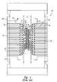
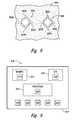
- a microelectronic device package 10can include a support member 20 having a front surface 21 and a rear surface 22 facing opposite the front surface 21 .
- the support member 20can also have a slot 23 extending from the front surface 21 to the rear surface 22 .
- a microelectronic substrate 40(visible through the slot 23 ) is attached to the rear surface 22 , and has wire bond pads 41 that are accessible through the slot 23 for coupling to the support member 20 .
- the support member 20can include active trace patterns 30 , each of which has a wire bond pad 32 , a ball bond pad 31 , and a connecting trace 33 extending between the wire bond pad 32 and the ball bond pad 31 .
- Each active trace pattern 30can also include an electroplating trace 34 coupled to an electroplating bus 24 to provide electrically conductive coatings on the active trace pattern 30 during the formation of the support member 20 .
- the wire bond pads 32 of the active trace patterns 30are connected to corresponding wire bond pads 41 of the microelectronic substrate 40 with wire bonds 42 .
- a solder ball(not shown in FIG. 1) can then be disposed on each ball bond pad 31 .
- the wire bonds 42 and the wire bond pads 41 and 32can then be covered with an encapsulating material for protection, while the solder balls remain exposed.
- the exposed solder ballscan be connected to other devices to provide for communication between those devices and the packaged microelectronic substrate 40 .
- the support member 20can include inactive trace patterns 50 .
- Each inactive trace pattern 50can include a ball bond pad 51 that supports a solder ball, and an electroplating trace 54 for electroplating conductive coatings on the inactive trace pattern 50 .
- the inactive trace patterns 50do not include a wire bond pad 32 or a corresponding connecting trace 33 . Accordingly, the inactive trace patterns 50 do not provide electrical communication to or from the microelectronic substrate 40 .
- the inactive trace patterns 50can support solder balls which, together with the solder balls on the active trace patterns 30 , define a uniform pattern of solder balls that can be compatible with a variety of devices in which the package 10 is installed and/or tested.
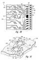
- FIG. 2illustrates a conventional test apparatus 60 for testing device packages such as the package 10 described above with reference to FIG. 1.
- the test apparatus 60can include a base 61 that supports the device package 10 .
- An overlying frame 62secures the package 10 to the base 61 .
- solder balls 25 of the package 10remain exposed through an opening 65 in the frame 62 .
- a test jig 63is then aligned with the base 61 such that test contacts 64 of the jig 63 make physical and electrical contact with the solder balls 25 of the package 10 .
- the test jig 63is then used to test the operational characteristics of the device package 10 .
- test jig 63can partially or completely dislodge some of the solder balls 25 and/or the trace patterns to which the solder balls 25 are connected.
- the dislodged solder balls 25 and/or trace patternscan increase the incidence of short circuits in the package 10 , and accordingly packages with these defects are typically discarded.
- An apparatus in according with one aspect of the inventionincludes a microelectronic substrate, a support member carrying the microelectronic substrate, and a connection structure carried by the support member.
- the connection structurecan have a bond site configured to receive a flowable conductive material, such as solder, and the connection site can further have at least two elongated members connected to and extending outwardly from the bond site. Each elongated member can be configured to receive at least a portion of the flowable conductive material from the bond site, and none of the elongated members is electrically coupled to the microelectronic substrate.
- connection structurecan be a first connection structure and the elongated members can be first elongated members.
- the apparatuscan include a second connection structure carried by the support member and having a second bond site configured to receive a flowable conductive material.
- the second connection structurecan be electrically coupled to the microelectronic substrate and can have second elongated members extending outwardly from the second bond site, with each of the second elongated members configured to receive at least a portion of the flowable conductive material from the second bond site.
- the number of second elongated members for each second connection structurecan equal the number of first elongated members for the first connection structure.
- the inventionis also directed to a method for coupling a flowable conductive material to a microelectronic substrate.
- the methodcan include aligning a support member to receive the flowable conductive material, with the support member having a support surface configured to carry a microelectronic substrate, and further having a first connection structure and second connection structure.
- the first connection structurecan have a first bond site configured to receive the flowable conductive material and can be configured to remain decoupled from the microelectronic substrate when a support member carries the microelectronic substrate.
- the second connection structurecan have a second bond site configured to receive the flowable conductive material, and can be configured to be electrically coupled to the microelectronic substrate when the support member carries the microelectronic substrate.
- the methodcan further include disposing a first quantity of the flowable conductive material on the first bond site, wicking a first portion of the first quantity of flowable material along first elongated members connected to and extending outwardly from the first bond site, and disposing a second quantity of the flowable conductive material on the second bond site.
- the methodcan further include wicking a second portion of the second quantity of flowable conductive material along second elongated members extending outwardly from the second bond site, with the second portion of the flowable conductive material having a volume approximately equal to a volume of the first portion.
- the first quantity of flowable conductive materialcan form a first conductive coupler
- the second quantitycan form a second conductive coupler
- each conductive couplercan project from the support member by approximately the same distance.
- FIG. 1is a bottom view of a microelectronic device package in accordance with the prior art, with selected features shown schematically.
- FIG. 2is a partially exploded illustration of a test apparatus for testing microelectronic device packages in accordance with the prior art.
- FIG. 3Ais a plan view of a support member having active and inactive connection structures in accordance with an embodiment of the invention.
- FIG. 3Bis an enlarged view of a portion of the support member shown in FIG. 3A, connected to a microelectronic substrate in accordance with an embodiment of the invention.
- FIG. 3Cis an isometric view of portions of active and inactive connection structures, with certain features shown schematically in accordance with an embodiment of the invention.
- FIG. 3Dis an enlarged plan view of another portion of the support member shown in FIG. 3A, connected to a microelectronic substrate in accordance with an embodiment of the invention.
- FIG. 4is an enlarged plan view of a portion of a support member in accordance with another embodiment of the invention.
- FIG. 5is a plan view of a portion of a support member having active and inactive connection structures configured for electroplating in accordance with another embodiment of the invention.
- FIG. 6is a plan view of a portion of a support member having active and inactive connection structures configured for electroless plating in accordance with another embodiment of the invention.
- FIG. 7is a plan view of a portion of a support member having active and inactive connection structures configured for electroplating in accordance with yet another embodiment of the invention.
- FIG. 8is a plan view of a portion of a support member having active and inactive connection structures configured for electroless plating in accordance with still another embodiment of the invention.
- FIG. 9is a schematic illustration of a device that includes apparatuses in accordance with another aspect of the invention.
- FIG. 10is a cross-sectional side view of an apparatus including a microelectronic substrate and a connection structure in accordance with another embodiment of the invention.
- FIG. 11is a plan view of the apparatus shown in FIG. 10 in accordance with an embodiment of the invention.
- FIG. 12Ais a cross-sectional side view of an apparatus including a microelectronic substrate and a connection structure having elongated members in accordance with yet another embodiment of the invention.
- FIG. 12Bis a top isometric view of a portion of the apparatus shown in FIG. 12A.
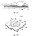
- FIG. 13Ais a cross-sectional side view of an apparatus including a microelectronic substrate and a connection structure in accordance with still another embodiment of the invention.
- FIG. 13Bis a top isometric view of a portion of the apparatus shown in FIG. 13A.
- FIG. 14is a top plan view of a support member in accordance with another embodiment of the invention.
- FIG. 15is a bottom plan view of the support member shown in FIG. 14 in accordance with an embodiment of the invention.
- microelectronic substrateis used throughout to include substrates upon which and/or in which microelectronic circuits or components, data storage elements or layers, and/or vias or conductive lines are or can be fabricated.
- microelectronic substrateis used throughout to include substrates upon which and/or in which microelectronic circuits or components, data storage elements or layers, and/or vias or conductive lines are or can be fabricated.
- the solder balls and/or trace patterns of the packaged devicecan become dislodged during testing, which typically requires discarding the package.
- the inactive solder balls and tracesmay become dislodged more frequently than the active solder balls and traces. Accordingly, in several of the embodiments described below, the inactive traces (or connection structures) are more securely attached to the support member, and/or are configured to be symmetric with the active traces (or connection structures).
- the solder balls or other conductive couplers disposed on the inactive connection structurescan have a size, shape and support generally similar to the size, shape and support of the conductive couplers disposed on the active connection structures.
- the packagecan be less likely to be damaged during testing or installation.
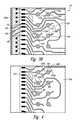
- FIG. 3Ais a plan view of an apparatus 110 having a support member 120 in accordance with an embodiment of the invention.
- the support member 120can have a first surface 121 that supports active connection structures 130 and inactive connection structures 150 .
- the first surface 121can also include plating buses 124 (shown in FIG. 3A as edge plating buses 124 a and a central plating bus 124 b ) that provide current for plating conductive materials onto the active connection structures 130 and the inactive connection structures 150 as these structures are manufactured.
- the support member 120can further include a second surface 122 facing in an opposite direction from the first surface 121 and configured to support a microelectronic substrate for coupling to the active connection structures 130 .
- the support member 120can include a relatively thin sheet of flexible, epoxy resin, such as BT (bimaleimide triazine) or another suitable material.
- FIG. 3Bis a detailed plan view of a portion of the apparatus 110 described above with reference to FIG. 3A, attached to a microelectronic substrate 140 .
- the central plating bus 124FIG. 3A
- the microelectronic substrate 140has been mounted to the second surface 122 of the support member 120 such that wire bond pads 141 of the microelectronic substrate 140 are accessible through the slot 123 for connecting to the active connection structures 130 on the first surface 121 of the support member 120 .
- the active connection structures 130can each include an active bond site 131 , such as a ball bond pad, which is configured to support a volume of a flowable conductive material, such as solder.
- a flowable conductive materialsuch as solder.
- the active connection structure 130can further include two active elongated members 133 , shown in FIG. 3B as active elongated members 133 a and 133 b .
- the active elongated member 133 aextends away from the slot 123 for connecting to the edge plating bus 124 a (FIG. 3A).
- the active elongated member 133 bextends between the active bond site 131 and a wire bond pad 132 positioned adjacent to the slot 123 .
- the wire bond pad 132can be connected with a wire bond 142 to a corresponding one of the wire bond pads 141 of the microelectronic substrate 140 to provide electrical communication between the wire bond pad 141 and the active bond site 131 .
- the inactive connection structures 150can each include an inactive bond site 151 , such as a ball bond pad, coupled to two inactive elongated members 153 , shown in FIG. 3B as inactive elongated members 153 a and 153 b . Accordingly, the inactive bond site 151 can support a flowable conductive material, such as a solder ball.
- the inactive elongated member 153 aextends away from the slot 123 for connecting to the edge plating bus 124 a (FIG. 3A).
- the inactive elongated member 153 bcan be shorter than the inactive elongated member 153 a to define an elongated tab shape, and can remain electrically decoupled from the microelectronic substrate 140 . Accordingly, the inactive bond sites 151 are not electrically connected to the microelectronic substrates 140 ; however, the solder balls they support (in combination with the solder balls of the active bond sites 131 ) can form a uniform pattern that is compatible with a variety of electronic devices and test fixtures.
- FIG. 3Cis an isometric view of a portion of the support member 120 showing an active connection structure 130 and an inactive connection structure 150 , each carrying a quantity of flowable conductive material 125 in accordance with an embodiment of the invention.
- the flowable conductive material 125can form conductive couplers 129 (such as solder balls), shown in FIG. 3C as an active conductive coupler 129 a supported by the active connection structure 130 , and an inactive conductive coupler 129 b supported by the inactive connection structure 150 .
- the active elongated members 133 a,b and the inactive elongated members 153 a,bcan include materials that are easily wetted by the flowable conductive material 125 .
- the elongated members 153 a,b and 133 a,bcan include nickel, gold, and/or copper or other metallic constituents. Accordingly, when the flowable conductive material 125 is disposed on the bond sites 131 and 151 , it tends to wick along the elongated members 133 a,b and 153 a,b , respectively. When the flowable conductive material 125 solidifies to form the conductive couplers 129 , it can have an at least partially ellipsoid shape.
- the support member 120can optionally include a cover layer 126 attached to the first surface 121 with the connection structures 130 and 150 disposed between the cover layer 126 and the first surface 121 .
- the cover layer 126can include a solder mask, and in other embodiments, the cover layer 126 can include other materials.
- the cover layer 126can have apertures 127 (shown as apertures 127 a and 127 b ) aligned with the bond sites 131 and 151 , respectively.
- the apertures 127are sized to leave the bond sites 131 and 151 exposed, while covering at least part of each elongated member 133 a,b and 153 a,b to aid in securing the elongated members to the support member 120 .
- the aperturesare sized to leave the bond sites 131 and 151 exposed while covering each elongated member 133 a,b and 153 a,b up to the edge of the corresponding bond site 131 , 151 .
- the elongated members 133 a,bcan be secured directly to the first surface 121 without the cover layer 126 .
- the bond sites 131 and 150can each have a diameter of about 330 microns, and each elongated member 133 a,b and 153 a,b (and in particular, the inactive elongated member 153 b ) can have a length L of at least 250 microns.
- the apertures 127 a,b in the cover layer 126can have a diameter of about 430 microns. Accordingly, each bond site 131 , 151 can be completely exposed through the corresponding aperture 127 a , 127 b .
- each elongated member 133 a,b and 153 a,bcan also be exposed for a distance D 1 of about 50 microns, measured from the edge of the corresponding bond site 131 , 151 , respectively.
- the elongated member 153 bcan be covered by the cover layer 126 for a distance D 2 of about 200 microns, and the remaining elongated members can be covered for distances greater than D 2 .
- the foregoing dimensionscan have other values.
- each elongated member 153 a,b and 133 a,bcan have approximately the same width W in a direction transverse to the elongation direction to increase the likelihood that the flowable conductive material 125 will wick along each elongated member in at least approximately the same way.
- the angular spacing between the active elongated members 133 a and 133 bcan be about the same as the angular spacing between the inactive elongated members 131 a and 131 b (about 180° in FIG. 3A-C).
- the number of inactive elongated members 153 extending away from the inactive bond site 151is equal to the number of active elongated members 133 extending away from the active bond site 131 . Accordingly, the cover layer 126 (or alternatively the elongated members alone) can provide approximately the same securing force to both the inactive connection structure 150 and the active connection structure 130 . As a result, the inactive elongated members 153 a,b can be less likely to pull away from the support member 120 when subjected to stresses, such as shear stresses which may be imposed on the conductive couplers 129 during testing.
- This featurecan apply when the cover layer 126 covers some or all of the elongated members, and/or when the cover layer 126 is not implemented. This is unlike some conventional arrangements (such as those described above with reference to FIGS. 1 and 2) for which the inactive connection structure may have fewer elongated members than the active connection structure and may accordingly be more likely to pull away from the support member when subjected to shear or other stresses.
- the inactive elongated members 153can wick away the flowable conductive material 125 in generally the same manner and to generally the same extent as the active elongated members 133 .
- the number of inactive elongated members 153 extending away from each inactive bond site 151can be the same as the number of active elongated members 133 extending away from each active bond site 131 , the flowable conductive material 125 will tend to wick away from both bond sites in generally the same way. Accordingly, approximately the same volume of flowable conductive material will tend to wick along each elongated member and away from each bond site, whether the bond site is active or inactive.
- the angular spacing between adjacent inactive elongated members 153can be about the same as the angular spacing between adjacent active elongated members 133 .
- the overall size and shape of flowable conductive material 125 remaining on the inactive bond site 151 (forming the inactive conductive coupler 129 b )can be approximately the same as the overall size and shape of the flowable conductive material 125 remaining on the active bond site 131 (forming the active conductive coupler 129 a ).
- the height H 2 by which the inactive conductive coupler 129 b projects from the support member 120can be at least approximately the same as the height H 1 by which the active conductive coupler 129 a projects from the support member 120 .
- the distance D 1can be at least approximately the same for both the active elongated members 133 a,b and the inactive elongated members 153 a,b .
- the flowable conductive material 125(which tends to wick along the exposed portions of the elongated members, but not beneath the cover layer 126 ) can wick away from the inactive bond site 151 in generally the same manner and to generally the same extent as it wicks away from the active bond site 131 .
- the shape of the inactive conductive coupler 129 bcan be at least approximately identical to the shape of the active conductive coupler 129 a.
- the inactive conductive couplers 129 bcan be contacted by a conventional test fixture (such as the fixture 60 shown in FIG. 2) in generally the same manner as are the active conductive couplers 129 a because the shapes and sizes of the conductive couplers 129 a,b are about the same.
- a conventional test fixturesuch as the fixture 60 shown in FIG. 2
- the inactive solder ballsmay project from the support member by a greater distance than the active solder balls because the solder disposed on the inactive ball bond pads has fewer avenues along which to wick away.
- the inactive solder ballsmay come under greater stress during testing and may be more likely to become dislodged.
- FIG. 3Dis an enlarged plan view of another portion of the apparatus 110 described above with reference to FIG. 3A.
- Three of the active connection structures 130 shown in FIG. 3Dhave an electroplating trace 134 connected between the central plating bus 124 b and the corresponding wire bond pad 132 .
- These active connection structures 130also have an active elongated member 133 a extending between the wire bond pad 132 and the corresponding bond site 131 .
- These active connection structures 130can further include an active elongated member 133 b having an elongated tab shape generally similar to that of the inactive elongated members 153 b described above. Accordingly, the active connection structures 130 and the inactive connection structure 150 shown in FIG.
- 3Dcan each have the same number of elongated members extending from the corresponding bond sites, and can accordingly carry conductive couplers (not shown in FIG. 3D) having at least approximately similar shapes in a manner generally similar to that described above with reference to FIGS. 3 A-C.
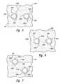
- FIGS. 4 - 8illustrate support members with connection structures having arrangements in accordance with further embodiments of the invention.
- FIG. 4illustrates a support member 420 having an active connection structure 430 and an inactive connection structure 450 , neither of which includes an electroplating trace. Accordingly, the support member 420 can be processed electrolessly to plate the connection structures 430 and 450 during manufacturing.
- the active connection structure 430can include an active bond site 431 having an active elongated member 433 a connected to a corresponding wire bond pad 432 in a manner generally similar to that described above.
- the active connection structure 430can also include a tab-shaped active elongated member 433 b extending away from the active bond site 431 .
- the inactive connection structure 450can include an inactive bond site 451 and two inactive elongated members 453 a and 453 b .
- the inactive elongated member 453 bcan include an anchor 455 which can increase the strength of the connection between the inactive connection structure 450 and the support member 420 .
- the anchor 455can provide more surface area beneath the corresponding cover layer 126 (not shown in FIG. 4), which can further reduce the likelihood for tearing the inactive connection structure 450 away from the support member 420 when the inactive connection structure 450 is subjected to a shear stress.
- the anchor 455can have a generally triangular shape, and in other embodiments, the anchor 455 can have other shapes. In still further embodiments, the anchor 455 can be included as part of any of the elongated members described above or below, when space permits.
- FIG. 5illustrates an embodiment of a support member 520 having an active connection structure 530 with three active elongated members 533 a , 533 b and 533 c .
- the support member 520can further include an inactive connection structure 550 having three inactive elongated members 553 a , 553 b and 553 c .
- the elongated members 533 a and 553 acan be coupled to an edge plating bus (not shown in FIG. 5), and the elongated member 533 b can be coupled to a wire bond pad (not shown in FIG. 5) in a manner generally similar to that described above.
- the elongated members 533 a , 533 b and 553 a , as well as the elongated members 533 c , 553 b and 553 c(which are not connected to other conductive structures) can extend beneath a cover layer 526 to secure the connection structures to the support member 520 , as was generally discussed above.
- the cover layer 526can be eliminated and the elongated members can be secured to the support member 520 with other techniques.
- the active connection structure 530 and the inactive connection structure 550can each include the same number of elongated members and can accordingly support conductive couplers having at least approximately similar shapes and sizes.
- each elongated membercan be angularly spaced apart from its neighbor by about 120°.
- the angular spacingcan have other values for which the angular spacings for the active elongated members 533 a - c are at least generally similar to those for the inactive elongated members 553 a - c.
- FIG. 6illustrates a support member 620 having an active connection structures 630 and an inactive connection structures 650 .
- connection structuresare generally similar to the connection structures described above except that the connection structures 630 and 650 are configured for electroless plating.
- the active connection structure 630can include an active elongated member 633 b coupled to a wire bond pad (not shown in FIG. 6), and can also include two tab-shaped elongated members 633 a and 633 c that are not connected to other conductive structures. All three inactive elongated members 653 a - c can be unconnected to other conductive structures.
- FIG. 7illustrates a support member 720 having an active connection structure 730 with four active elongated members 733 a - d , and an inactive connection structure 750 having four inactive elongated members 753 a - d .
- the elongated members 733 a and 753 aare each configured to be coupled to a plating bus in a manner generally similar to that described above with reference to FIGS. 3B and 5.
- each elongated memberis angularly spaced apart from its neighbor by about 90°.
- the angular spacingcan have other values with the angular spacing between adjacent active elongated members 733 a - d being approximately the same as the angular spacing between inactive elongated members 753 a - d , and the number of active elongated members 733 being the same as the number of inactive elongated members.
- FIG. 8illustrates a support member 820 having an active connection structure 830 and an inactive connection structure 850 , each configured for electroless plating.
- the active connection structure 830can have four active elongated members 833 a - d .
- the inactive connection structure 850can have four inactive elongated members 853 a - d .
- the number of and spacing between active elongated members 833 a - dcan be at least approximately the same as for the inactive elongated members 853 a - d.
- the active and inactive connection structurescan have other shapes and arrangements for which the number of elongated members extending outwardly from an active bond site is equal to the number of elongated members extending outwardly from an inactive bond site.
- the connection structures and, optionally, the corresponding cover layerscan support conductive couplers (such as solder balls) having generally similar shapes and similar behaviors, regardless of whether the conductive couplers are carried by an active bond site or an inactive bond site.
- FIG. 9is a schematic illustration of an electronic device 970 that includes one or more apparatuses 910 in accordance with an embodiment of the invention.
- the electronic devicecan include a computer, a telecommunication device or another device that incorporates microelectronic components.
- the device 910can include a housing 971 containing a processor 973 , a memory 972 and/or an input/output device 974 , each of which can include an apparatus 910 generally similar to any of the apparatuses described above with reference to FIGS. 3 A- 8 .
- the device 910can also include other apparatuses 910 in addition to or in lieu of the apparatuses incorporated into the processor 973 , the memory 972 and/or the input/output device 974 .
- FIG. 10is a cross-sectional side view of an apparatus 1010 that includes a microelectronic substrate 1040 having a connection structure 1030 disposed on it in accordance with another embodiment of the invention.
- the microelectronic substrate 1040can have a first surface 1045 and a second surface 1046 facing opposite from the first surface 1045 .
- the microelectronic substrate 1040can further include active microelectronic features 1044 positioned proximate to the second surface 1046 , and a first bond site 1041 (such as a bond pad), also positioned proximate to the second surface 1046 .
- the connection structure 1030can include a second bond site 1031 spaced apart from the first bond site 1041 .
- the second bond site 1031can include a solder ball pad, and can support a conductive coupler 1029 , such as a solder ball.
- the appuratus 1010can have a “flip chip” configuration.
- the second bond site 1031can have other configurations and can support other types of conductive couplers.
- the connection structure 1030can include an electrically conductive material (such as a metal redistribution layer) and can have a first surface 1037 facing toward the second surface 1046 of the microelectronic substrate 1040 , and a second surface 1038 facing opposite from the first surface 1037 .
- connection structure 1030can further include elongated members 1033 a and 1033 b extending outwardly from the second bond site 1031 .
- the elongated member 1033 acan be connected between the second bond site 1031 of the connection structure and the first bond site 1041 of the microelectronic substrate 1040 .
- the elongated member 1033 bcan have a generally tab-shaped configuration, generally similar to those described above.
- the apparatus 1010can include passivation layers 1035 (shown as a first passivation layer 1035 a and a second passivation layer 1035 b ) positioned between electrically conductive elements of the apparatus 1010 to at least partially isolate these elements from each other.
- the first passivation layer 1035 acan be positioned between the second surface 1046 (including the active microelectronic features 1044 ) of the microelectronic substrate 1040 , and the first surface 1037 of the connection structure 1030 .
- the second passivation layer 1035 bcan be positioned adjacent to the second surface 1038 of the connection structure 1030 .
- the second passivation layer 1035 bcan perform at least some of the same functions as the cover layer 126 described above reference to FIG. 3C. Accordingly, the second passivation layer 1035 b can aid in securing the connection structure 1030 to the microelectronic substrate 1044 . In one embodiment, the second passivation layer 1035 b can extend over the entire lengths of the elongated members 1033 a , 1033 b , while leaving the second connection site 1031 exposed to receive the conductive coupler 1029 .
- FIG. 11is a plan view of an embodiment of the apparatus 1010 described above with reference to FIG. 10.
- each of the elongated members 1033 acan extend between the corresponding first bond site 1041 of the microelectronic substrate 1040 and the corresponding second bond site 1031 , and can be generally co-planer with each other.
- the elongated members 1033 acan cross over each other, for example, by extending into different planes normal to the plane of FIG. 11 to avoid electrical contact with the elongated members over which they pass.
- the apparatus 1010can include an inactive connection structure 1150 having a second bond site 1151 .
- Elongated members 1153 a , 1153 bcan extend outwardly from the second bond site 1151 , without being electrically connected to the microelectronic substrate 1040 .
- the inactive connection structures 1150can support a conductive coupler to provide uniformity with a pre-selected pattern of conductive couplers, in a manner generally similar to that described above.
- FIGS. 12 A-Billustrate a cross-sectional side view and top isometric view, respectively, of an apparatus 1210 in accordance with another embodiment of the invention.
- the apparatus 1210can include a microelectronic substrate 1240 having a first bond site 1241 , and a connection structure 1230 having a second bond site 1231 .
- the microelectronic substrate 1240can include active devices 1244 electrically coupled to the first bond site 1241 .
- the connection structure 1230can include a plurality of elongated members 1233 (two are shown in FIGS. 12 A-B as elongated members 1233 a , 1233 b ) extending outwardly from the second bond site 1231 .
- the elongated member 1233 acan be coupled between the first bond site 1241 and the second bond site 1231 , and the elongated member 1233 b can include an elongated tab-shaped member generally similar to those described above.
- the bond site 1231can include a support portion 1280 carrying a wettable portion 1281 .
- the support portion 1280can have a composition generally similar to that of the elongated members 1233 a - 1233 b (for example, a composite of aluminum, nickel, copper and titanium), and the wettable portion 1281 can have a different composition (such as a composite of nickel and copper). Accordingly, the wettable portion 1281 can be configured to be wetted by a flowable conductive material (such as solder) to support and electrically couple to a conductive coupler 1229 .
- a flowable conductive materialsuch as solder
- the apparatus 1210can include a die passivation layer 1235 positioned between the active devices 1244 and the connection structure 1230 .
- a first dielectric layer 1236 acan be disposed between the passivation layer 1235 and the elongated members 1233 a , 1233 b
- a second dielectric layer 1236 bcan be disposed on top of the connection structure 1230 .
- the elongated members 1233 a , 1233 bare not wetted by the conductive coupler 1229 because the wettable portion 1281 of the second bond site 1231 does not extend over the elongated members.
- the elongated members 1233 a , 1233 bcan be wetted by the conductive coupler 1229 in a manner generally similar to that described above with reference to FIG. 3C.
- FIG. 13Ais a cross-sectional side view of an apparatus 1310 having a connection structure 1330 in accordance with another embodiment of the invention.
- FIG. 13Bis a top isometric view of a portion of the apparatus 1310 shown in FIG. 13A.
- the apparatus 1310can include a microelectronic substrate 1340 having a first bond site 1341 , a passivation layer 1335 , and a first dielectric layer 1336 a disposed on the passivation layer 1335 .
- the connection structure 1330can be disposed on the first dielectric layer 1336 a and can include a second bond site 1331 electrically connected to the first bond site 1341 with a connecting trace 1333 .
- the second bond site 1331can include a generally circular first portion 1382 positioned on the first dielectric layer 1336 a and electrically connected to the connecting trace 1333 .
- a second dielectric layer 1336 bcan be disposed on the connection structure 1330 , including the first portion 1382 of the second bond site 1331 .
- the second bond site 1331can further include a second portion 1383 electrically connected to the first portion 1382 and having at least two elongated members 1333 a , 1333 b extending outwardly therefrom over the second dielectric layer 1336 b .
- the first portion 1382can include a composite of titanium and either copper or aluminum
- the second portion 1383can include a composite of titanium, copper, and nickel.
- these componentscan include other constituents.
- the elongated member 1333 a , 1333 bcan provide some or all of the advantages described above with reference to the foregoing figures.
- FIG. 14illustrates a top plan view of a support member 1420 for supporting a microelectronic substrate in accordance with another embodiment of the invention.
- the support member 1420can include a first surface 1421 and a second surface 1422 facing opposite from the first surface 1421 .
- the second surface 1422can be configured to carry a microelectronic substrate.
- the support member 1420can include connection structures 1430 for connecting the microelectronic substrate supported on the support member 1420 to other electronic or microelectronic devices.
- each connection structure 1430can include a first bond site (such as a solder pad) described below with reference to FIG.
- connection structure 1430can further include electroplating traces 1434 configured to connect to a source of electrical potential for plating the connection structure 1430 , generally in a manner similar to that described above.
- connection structures 1430can be plated with an electroless process.
- connection structures 1430can further include a connecting trace 1439 that extends outwardly from the second bond site 1432 .
- the connecting trace 1439can be coupled to a via 1436 that extends from the second surface of the support member 1420 to the first surface 1421 .
- the via 1436can be electrically coupled to the first bond site of the support member 1420 , as described in greater detail below with reference to FIG. 15.
- FIG. 15is a bottom plan view of an embodiment of the support member 1420 described above with reference to FIG. 14.
- each of the vias 1436 of the connection structures 1430can extend through the support member 1420 to the first surface 1421 .
- Each via 1436can be electrically connected to a corresponding first bond site 1431 (such as a solder ball pad), to provide for electrical communication between the first bond site 1431 and the second bond site 1432 (FIG. 14) on the opposite side of the support member.
- each connection structure 1430can include at least two elongated members 1433 a , 1433 b extending outwardly from the first bond site 1431 .
- the elongated member 1433 bcan extend between the first bond site 1431 and the via 1436 to provide for electrical communication between these two components of the connection structure 1430 .
- the elongated member 1433 acan include a generally tab-shaped structure generally similar to those described above. Accordingly, the elongated members 1433 a , 1433 b can provide some or all of the functions and advantages described above with reference to FIGS. 3 A- 8 .
- the elongated members 1433 a , 1433 bcan aid in securing the first bond site 1431 to the first surface 1421 of the support member 1420 .
- the support member 1420can include a cover layer generally similar to that described above with reference to FIG. 3C to aid in attaching the connection structure 1430 to the first surface 1421 . Accordingly, the cover layer can be configured to either allow or prevent wicking of a flowable conductive material along the elongated members 1433 a , 1433 b.
Landscapes
- Engineering & Computer Science (AREA)
- Microelectronics & Electronic Packaging (AREA)
- Physics & Mathematics (AREA)
- Condensed Matter Physics & Semiconductors (AREA)
- General Physics & Mathematics (AREA)
- Computer Hardware Design (AREA)
- Power Engineering (AREA)
- Geometry (AREA)
- Wire Bonding (AREA)
- Electric Connection Of Electric Components To Printed Circuits (AREA)
- Measuring Leads Or Probes (AREA)
Abstract
Description
- The present invention is directed toward methods and apparatuses for supporting microelectronic substrates. Conventional microelectronic device packages typically include a microelectronic substrate mounted on a support member and packaged with an encapsulant. In one conventional arrangement shown in FIG. 1, a[0001]
microelectronic device package 10 can include asupport member 20 having afront surface 21 and arear surface 22 facing opposite thefront surface 21. Thesupport member 20 can also have aslot 23 extending from thefront surface 21 to therear surface 22. A microelectronic substrate40 (visible through the slot23) is attached to therear surface 22, and haswire bond pads 41 that are accessible through theslot 23 for coupling to thesupport member 20. Accordingly, thesupport member 20 can includeactive trace patterns 30, each of which has awire bond pad 32, aball bond pad 31, and a connectingtrace 33 extending between thewire bond pad 32 and theball bond pad 31. Eachactive trace pattern 30 can also include anelectroplating trace 34 coupled to anelectroplating bus 24 to provide electrically conductive coatings on theactive trace pattern 30 during the formation of thesupport member 20. - In operation, the[0002]
wire bond pads 32 of theactive trace patterns 30 are connected to correspondingwire bond pads 41 of themicroelectronic substrate 40 withwire bonds 42. A solder ball (not shown in FIG. 1) can then be disposed on eachball bond pad 31. Thewire bonds 42 and thewire bond pads microelectronic substrate 40. - In order to conform with industry standards,[0003]
similar device packages 10 are often required to have the same number of solder balls, even if not all the solder balls are required to provide communication with themicroelectronic substrate 40. Accordingly, thesupport member 20 can includeinactive trace patterns 50. Eachinactive trace pattern 50 can include aball bond pad 51 that supports a solder ball, and anelectroplating trace 54 for electroplating conductive coatings on theinactive trace pattern 50. Theinactive trace patterns 50 do not include awire bond pad 32 or acorresponding connecting trace 33. Accordingly, theinactive trace patterns 50 do not provide electrical communication to or from themicroelectronic substrate 40. However, theinactive trace patterns 50 can support solder balls which, together with the solder balls on theactive trace patterns 30, define a uniform pattern of solder balls that can be compatible with a variety of devices in which thepackage 10 is installed and/or tested. - FIG. 2 illustrates a[0004]
conventional test apparatus 60 for testing device packages such as thepackage 10 described above with reference to FIG. 1. In one aspect of this arrangement, thetest apparatus 60 can include abase 61 that supports thedevice package 10. Anoverlying frame 62 secures thepackage 10 to thebase 61. When thepackage 10 is secured to thebase 61,solder balls 25 of thepackage 10 remain exposed through anopening 65 in theframe 62. Atest jig 63 is then aligned with thebase 61 such thattest contacts 64 of thejig 63 make physical and electrical contact with thesolder balls 25 of thepackage 10. Thetest jig 63 is then used to test the operational characteristics of thedevice package 10. - One drawback with the foregoing arrangement is that the[0005]
test jig 63 can partially or completely dislodge some of thesolder balls 25 and/or the trace patterns to which thesolder balls 25 are connected. The dislodgedsolder balls 25 and/or trace patterns can increase the incidence of short circuits in thepackage 10, and accordingly packages with these defects are typically discarded. - The present invention is directed toward methods and apparatuses for supporting microelectronic substrates. An apparatus in according with one aspect of the invention includes a microelectronic substrate, a support member carrying the microelectronic substrate, and a connection structure carried by the support member. The connection structure can have a bond site configured to receive a flowable conductive material, such as solder, and the connection site can further have at least two elongated members connected to and extending outwardly from the bond site. Each elongated member can be configured to receive at least a portion of the flowable conductive material from the bond site, and none of the elongated members is electrically coupled to the microelectronic substrate.[0006]
- In a further aspect of the invention, the connection structure can be a first connection structure and the elongated members can be first elongated members. The apparatus can include a second connection structure carried by the support member and having a second bond site configured to receive a flowable conductive material. The second connection structure can be electrically coupled to the microelectronic substrate and can have second elongated members extending outwardly from the second bond site, with each of the second elongated members configured to receive at least a portion of the flowable conductive material from the second bond site. The number of second elongated members for each second connection structure can equal the number of first elongated members for the first connection structure.[0007]
- The invention is also directed to a method for coupling a flowable conductive material to a microelectronic substrate. The method can include aligning a support member to receive the flowable conductive material, with the support member having a support surface configured to carry a microelectronic substrate, and further having a first connection structure and second connection structure. The first connection structure can have a first bond site configured to receive the flowable conductive material and can be configured to remain decoupled from the microelectronic substrate when a support member carries the microelectronic substrate. The second connection structure can have a second bond site configured to receive the flowable conductive material, and can be configured to be electrically coupled to the microelectronic substrate when the support member carries the microelectronic substrate. The method can further include disposing a first quantity of the flowable conductive material on the first bond site, wicking a first portion of the first quantity of flowable material along first elongated members connected to and extending outwardly from the first bond site, and disposing a second quantity of the flowable conductive material on the second bond site. The method can further include wicking a second portion of the second quantity of flowable conductive material along second elongated members extending outwardly from the second bond site, with the second portion of the flowable conductive material having a volume approximately equal to a volume of the first portion. The first quantity of flowable conductive material can form a first conductive coupler, the second quantity can form a second conductive coupler, and each conductive coupler can project from the support member by approximately the same distance.[0008]
- FIG. 1 is a bottom view of a microelectronic device package in accordance with the prior art, with selected features shown schematically.[0009]
- FIG. 2 is a partially exploded illustration of a test apparatus for testing microelectronic device packages in accordance with the prior art.[0010]
- FIG. 3A is a plan view of a support member having active and inactive connection structures in accordance with an embodiment of the invention.[0011]
- FIG. 3B is an enlarged view of a portion of the support member shown in FIG. 3A, connected to a microelectronic substrate in accordance with an embodiment of the invention.[0012]
- FIG. 3C is an isometric view of portions of active and inactive connection structures, with certain features shown schematically in accordance with an embodiment of the invention.[0013]
- FIG. 3D is an enlarged plan view of another portion of the support member shown in FIG. 3A, connected to a microelectronic substrate in accordance with an embodiment of the invention.[0014]
- FIG. 4 is an enlarged plan view of a portion of a support member in accordance with another embodiment of the invention.[0015]
- FIG. 5 is a plan view of a portion of a support member having active and inactive connection structures configured for electroplating in accordance with another embodiment of the invention.[0016]
- FIG. 6 is a plan view of a portion of a support member having active and inactive connection structures configured for electroless plating in accordance with another embodiment of the invention.[0017]
- FIG. 7 is a plan view of a portion of a support member having active and inactive connection structures configured for electroplating in accordance with yet another embodiment of the invention.[0018]
- FIG. 8 is a plan view of a portion of a support member having active and inactive connection structures configured for electroless plating in accordance with still another embodiment of the invention.[0019]
- FIG. 9 is a schematic illustration of a device that includes apparatuses in accordance with another aspect of the invention.[0020]
- FIG. 10 is a cross-sectional side view of an apparatus including a microelectronic substrate and a connection structure in accordance with another embodiment of the invention.[0021]
- FIG. 11 is a plan view of the apparatus shown in FIG. 10 in accordance with an embodiment of the invention.[0022]
- FIG. 12A is a cross-sectional side view of an apparatus including a microelectronic substrate and a connection structure having elongated members in accordance with yet another embodiment of the invention.[0023]
- FIG. 12B is a top isometric view of a portion of the apparatus shown in FIG. 12A.[0024]
- FIG. 13A is a cross-sectional side view of an apparatus including a microelectronic substrate and a connection structure in accordance with still another embodiment of the invention.[0025]
- FIG. 13B is a top isometric view of a portion of the apparatus shown in FIG. 13A.[0026]
- FIG. 14 is a top plan view of a support member in accordance with another embodiment of the invention.[0027]
- FIG. 15 is a bottom plan view of the support member shown in FIG. 14 in accordance with an embodiment of the invention.[0028]
- The present disclosure describes packaged microelectronic substrates and methods for forming such packages. The term “microelectronic substrate” is used throughout to include substrates upon which and/or in which microelectronic circuits or components, data storage elements or layers, and/or vias or conductive lines are or can be fabricated. Many specific details of certain embodiments of the invention are set forth in the following description and in FIGS.[0029]3A-9 to provide a thorough understanding of these embodiments. One skilled in the art, however, will understand that the present invention may have additional embodiments, and that the invention may be practiced without several of the details described below.
- As described above with reference to FIGS. 1 and 2, a drawback with some conventional arrangements is that the solder balls and/or trace patterns of the packaged device can become dislodged during testing, which typically requires discarding the package. In some cases, it has been observed that the inactive solder balls and traces may become dislodged more frequently than the active solder balls and traces. Accordingly, in several of the embodiments described below, the inactive traces (or connection structures) are more securely attached to the support member, and/or are configured to be symmetric with the active traces (or connection structures). Accordingly, the solder balls or other conductive couplers disposed on the inactive connection structures can have a size, shape and support generally similar to the size, shape and support of the conductive couplers disposed on the active connection structures. As a result, the package can be less likely to be damaged during testing or installation.[0030]
- FIG. 3A is a plan view of an[0031]
apparatus 110 having asupport member 120 in accordance with an embodiment of the invention. Thesupport member 120 can have afirst surface 121 that supportsactive connection structures 130 andinactive connection structures 150. Thefirst surface 121 can also include plating buses124 (shown in FIG. 3A asedge plating buses 124aand acentral plating bus 124b) that provide current for plating conductive materials onto theactive connection structures 130 and theinactive connection structures 150 as these structures are manufactured. Thesupport member 120 can further include asecond surface 122 facing in an opposite direction from thefirst surface 121 and configured to support a microelectronic substrate for coupling to theactive connection structures 130. Thesupport member 120 can include a relatively thin sheet of flexible, epoxy resin, such as BT (bimaleimide triazine) or another suitable material. - FIG. 3B is a detailed plan view of a portion of the[0032]
apparatus 110 described above with reference to FIG. 3A, attached to amicroelectronic substrate 140. As shown in FIG. 3B, the central plating bus124 (FIG. 3A) has been removed to form aslot 123 that extends through thesupport member 120 from thefirst surface 121 to thesecond surface 122. Themicroelectronic substrate 140 has been mounted to thesecond surface 122 of thesupport member 120 such thatwire bond pads 141 of themicroelectronic substrate 140 are accessible through theslot 123 for connecting to theactive connection structures 130 on thefirst surface 121 of thesupport member 120. - The[0033]
active connection structures 130 can each include anactive bond site 131, such as a ball bond pad, which is configured to support a volume of a flowable conductive material, such as solder. When the flowable conductive material is disposed on theactive bond site 131 and placed in a flowable state (for example, in a solder reflow oven), it can form an at least partially spherical or globular shape suitable for electrically and physically connecting theactive connection structure 130 to other devices or circuit elements. Theactive connection structure 130 can further include two active elongated members133, shown in FIG. 3B as activeelongated members elongated member 133aextends away from theslot 123 for connecting to theedge plating bus 124a(FIG. 3A). The activeelongated member 133bextends between theactive bond site 131 and awire bond pad 132 positioned adjacent to theslot 123. Thewire bond pad 132 can be connected with awire bond 142 to a corresponding one of thewire bond pads 141 of themicroelectronic substrate 140 to provide electrical communication between thewire bond pad 141 and theactive bond site 131. - The[0034]
inactive connection structures 150 can each include aninactive bond site 151, such as a ball bond pad, coupled to two inactive elongated members153, shown in FIG. 3B as inactiveelongated members inactive bond site 151 can support a flowable conductive material, such as a solder ball. The inactiveelongated member 153aextends away from theslot 123 for connecting to theedge plating bus 124a(FIG. 3A). The inactiveelongated member 153bcan be shorter than the inactiveelongated member 153ato define an elongated tab shape, and can remain electrically decoupled from themicroelectronic substrate 140. Accordingly, theinactive bond sites 151 are not electrically connected to themicroelectronic substrates 140; however, the solder balls they support (in combination with the solder balls of the active bond sites131) can form a uniform pattern that is compatible with a variety of electronic devices and test fixtures. - FIG. 3C is an isometric view of a portion of the[0035]
support member 120 showing anactive connection structure 130 and aninactive connection structure 150, each carrying a quantity of flowableconductive material 125 in accordance with an embodiment of the invention. Accordingly, the flowableconductive material 125 can form conductive couplers129 (such as solder balls), shown in FIG. 3C as an activeconductive coupler 129asupported by theactive connection structure 130, and an inactiveconductive coupler 129bsupported by theinactive connection structure 150. In one aspect of this embodiment, the activeelongated members 133a,band the inactiveelongated members 153a,bcan include materials that are easily wetted by the flowableconductive material 125. For example, when the flowableconductive material 125 includes solder, theelongated members 153a,band133a,bcan include nickel, gold, and/or copper or other metallic constituents. Accordingly, when the flowableconductive material 125 is disposed on thebond sites elongated members 133a,band153a,b, respectively. When the flowableconductive material 125 solidifies to form the conductive couplers129, it can have an at least partially ellipsoid shape. - In a further aspect of this embodiment, the[0036]
support member 120 can optionally include acover layer 126 attached to thefirst surface 121 with theconnection structures cover layer 126 and thefirst surface 121. In one embodiment, thecover layer 126 can include a solder mask, and in other embodiments, thecover layer 126 can include other materials. In any of these embodiments, thecover layer 126 can have apertures127 (shown asapertures bond sites bond sites elongated member 133a,band153a,bto aid in securing the elongated members to thesupport member 120. In an alternative embodiment (shown in dashed lines in FIG. 3C) the apertures are sized to leave thebond sites elongated member 133a,band153a,bup to the edge of thecorresponding bond site elongated members 133a,bcan be secured directly to thefirst surface 121 without thecover layer 126. - In one embodiment, the[0037]
bond sites elongated member 133a,band153a,b(and in particular, the inactiveelongated member 153b) can have a length L of at least 250 microns. Theapertures 127a,bin thecover layer 126 can have a diameter of about 430 microns. Accordingly, eachbond site aperture portion 128 of eachelongated member 133a,band153a,bcan also be exposed for a distance D1of about 50 microns, measured from the edge of thecorresponding bond site elongated member 153bcan be covered by thecover layer 126 for a distance D2of about 200 microns, and the remaining elongated members can be covered for distances greater than D2. In other embodiments, the foregoing dimensions can have other values. - In a further aspect of this embodiment, each[0038]
elongated member 153a,band133a,bcan have approximately the same width W in a direction transverse to the elongation direction to increase the likelihood that the flowableconductive material 125 will wick along each elongated member in at least approximately the same way. In yet a further aspect of this embodiment, the angular spacing between the activeelongated members - One feature of the foregoing arrangement is that the number of inactive elongated members[0039]153 extending away from the
inactive bond site 151 is equal to the number of active elongated members133 extending away from theactive bond site 131. Accordingly, the cover layer126 (or alternatively the elongated members alone) can provide approximately the same securing force to both theinactive connection structure 150 and theactive connection structure 130. As a result, the inactiveelongated members 153a,bcan be less likely to pull away from thesupport member 120 when subjected to stresses, such as shear stresses which may be imposed on the conductive couplers129 during testing. This feature can apply when thecover layer 126 covers some or all of the elongated members, and/or when thecover layer 126 is not implemented. This is unlike some conventional arrangements (such as those described above with reference to FIGS. 1 and 2) for which the inactive connection structure may have fewer elongated members than the active connection structure and may accordingly be more likely to pull away from the support member when subjected to shear or other stresses. - Another feature of an embodiment of the arrangement described above with reference to FIGS.[0040]3A-C is that the inactive elongated members153 can wick away the flowable
conductive material 125 in generally the same manner and to generally the same extent as the active elongated members133. For example, because the number of inactive elongated members153 extending away from eachinactive bond site 151 can be the same as the number of active elongated members133 extending away from eachactive bond site 131, the flowableconductive material 125 will tend to wick away from both bond sites in generally the same way. Accordingly, approximately the same volume of flowable conductive material will tend to wick along each elongated member and away from each bond site, whether the bond site is active or inactive. - Another feature of an embodiment of the arrangement described above with reference to FIGS.[0041]3A-C is that the angular spacing between adjacent inactive elongated members153 can be about the same as the angular spacing between adjacent active elongated members133. As a result, the overall size and shape of flowable
conductive material 125 remaining on the inactive bond site151 (forming the inactiveconductive coupler 129b) can be approximately the same as the overall size and shape of the flowableconductive material 125 remaining on the active bond site131 (forming the activeconductive coupler 129a). For example, the height H2by which the inactiveconductive coupler 129bprojects from thesupport member 120 can be at least approximately the same as the height H1by which the activeconductive coupler 129aprojects from thesupport member 120. - Yet another feature of an embodiment of the arrangement describe above with reference to FIGS.[0042]3A-C is that the distance D1can be at least approximately the same for both the active
elongated members 133a,band the inactiveelongated members 153a,b. Accordingly, the flowable conductive material125 (which tends to wick along the exposed portions of the elongated members, but not beneath the cover layer126) can wick away from theinactive bond site 151 in generally the same manner and to generally the same extent as it wicks away from theactive bond site 131. As a result, the shape of the inactiveconductive coupler 129bcan be at least approximately identical to the shape of the activeconductive coupler 129a. - An advantage of the foregoing features is that the inactive[0043]
conductive couplers 129bcan be contacted by a conventional test fixture (such as thefixture 60 shown in FIG. 2) in generally the same manner as are the activeconductive couplers 129abecause the shapes and sizes of theconductive couplers 129a,bare about the same. This is unlike some conventional arrangements (such as the arrangement described above with reference to FIG. 1) in which the inactive solder balls may project from the support member by a greater distance than the active solder balls because the solder disposed on the inactive ball bond pads has fewer avenues along which to wick away. In such conventional arrangements, the inactive solder balls may come under greater stress during testing and may be more likely to become dislodged. - FIG. 3D is an enlarged plan view of another portion of the[0044]
apparatus 110 described above with reference to FIG. 3A. Three of theactive connection structures 130 shown in FIG. 3D have anelectroplating trace 134 connected between thecentral plating bus 124band the correspondingwire bond pad 132. Theseactive connection structures 130 also have an activeelongated member 133aextending between thewire bond pad 132 and thecorresponding bond site 131. Theseactive connection structures 130 can further include an activeelongated member 133bhaving an elongated tab shape generally similar to that of the inactiveelongated members 153bdescribed above. Accordingly, theactive connection structures 130 and theinactive connection structure 150 shown in FIG. 3D can each have the same number of elongated members extending from the corresponding bond sites, and can accordingly carry conductive couplers (not shown in FIG. 3D) having at least approximately similar shapes in a manner generally similar to that described above with reference to FIGS.3A-C. - FIGS.[0045]4-8 illustrate support members with connection structures having arrangements in accordance with further embodiments of the invention. For example, FIG. 4 illustrates a
support member 420 having anactive connection structure 430 and aninactive connection structure 450, neither of which includes an electroplating trace. Accordingly, thesupport member 420 can be processed electrolessly to plate theconnection structures active connection structure 430 can include anactive bond site 431 having an activeelongated member 433aconnected to a correspondingwire bond pad 432 in a manner generally similar to that described above. Theactive connection structure 430 can also include a tab-shaped activeelongated member 433bextending away from theactive bond site 431. - The[0046]
inactive connection structure 450 can include aninactive bond site 451 and two inactiveelongated members elongated member 453bcan include ananchor 455 which can increase the strength of the connection between theinactive connection structure 450 and thesupport member 420. For example, theanchor 455 can provide more surface area beneath the corresponding cover layer126 (not shown in FIG. 4), which can further reduce the likelihood for tearing theinactive connection structure 450 away from thesupport member 420 when theinactive connection structure 450 is subjected to a shear stress. In one embodiment, theanchor 455 can have a generally triangular shape, and in other embodiments, theanchor 455 can have other shapes. In still further embodiments, theanchor 455 can be included as part of any of the elongated members described above or below, when space permits. - FIG. 5 illustrates an embodiment of a[0047]
support member 520 having anactive connection structure 530 with three activeelongated members support member 520 can further include aninactive connection structure 550 having three inactiveelongated members 553a,553band553c. Theelongated members 533aand553acan be coupled to an edge plating bus (not shown in FIG. 5), and theelongated member 533bcan be coupled to a wire bond pad (not shown in FIG. 5) in a manner generally similar to that described above. Theelongated members elongated members cover layer 526 to secure the connection structures to thesupport member 520, as was generally discussed above. Alternatively, thecover layer 526 can be eliminated and the elongated members can be secured to thesupport member 520 with other techniques. In either embodiment, theactive connection structure 530 and theinactive connection structure 550 can each include the same number of elongated members and can accordingly support conductive couplers having at least approximately similar shapes and sizes. In a further aspect of this embodiment, each elongated member can be angularly spaced apart from its neighbor by about 120°. In other embodiments, the angular spacing can have other values for which the angular spacings for the active elongated members533a-care at least generally similar to those for the inactive elongated members553a-c. - FIG. 6 illustrates a[0048]
support member 620 having anactive connection structures 630 and aninactive connection structures 650. These connection structures are generally similar to the connection structures described above except that theconnection structures active connection structure 630 can include an activeelongated member 633bcoupled to a wire bond pad (not shown in FIG. 6), and can also include two tab-shapedelongated members 633aand633cthat are not connected to other conductive structures. All three inactive elongated members653a-ccan be unconnected to other conductive structures. - FIG. 7 illustrates a[0049]
support member 720 having anactive connection structure 730 with four active elongated members733a-d, and aninactive connection structure 750 having four inactive elongated members753a-d. Theelongated members - FIG. 8 illustrates a[0050]
support member 820 having anactive connection structure 830 and aninactive connection structure 850, each configured for electroless plating. Accordingly, theactive connection structure 830 can have four active elongated members833a-d. Theinactive connection structure 850 can have four inactive elongated members853a-d. As described above, the number of and spacing between active elongated members833a-dcan be at least approximately the same as for the inactive elongated members853a-d. - In other embodiments, the active and inactive connection structures can have other shapes and arrangements for which the number of elongated members extending outwardly from an active bond site is equal to the number of elongated members extending outwardly from an inactive bond site. In any of these arrangements, the connection structures and, optionally, the corresponding cover layers, can support conductive couplers (such as solder balls) having generally similar shapes and similar behaviors, regardless of whether the conductive couplers are carried by an active bond site or an inactive bond site.[0051]
- FIG. 9 is a schematic illustration of an[0052]
electronic device 970 that includes one ormore apparatuses 910 in accordance with an embodiment of the invention. In one aspect of this embodiment, the electronic device can include a computer, a telecommunication device or another device that incorporates microelectronic components. Accordingly, thedevice 910 can include ahousing 971 containing aprocessor 973, amemory 972 and/or an input/output device 974, each of which can include anapparatus 910 generally similar to any of the apparatuses described above with reference to FIGS.3A-8. Thedevice 910 can also includeother apparatuses 910 in addition to or in lieu of the apparatuses incorporated into theprocessor 973, thememory 972 and/or the input/output device 974. - FIG. 10 is a cross-sectional side view of an[0053]
apparatus 1010 that includes amicroelectronic substrate 1040 having aconnection structure 1030 disposed on it in accordance with another embodiment of the invention. In one aspect of this embodiment, themicroelectronic substrate 1040 can have afirst surface 1045 and asecond surface 1046 facing opposite from thefirst surface 1045. Themicroelectronic substrate 1040 can further include activemicroelectronic features 1044 positioned proximate to thesecond surface 1046, and a first bond site1041 (such as a bond pad), also positioned proximate to thesecond surface 1046. - The[0054]
connection structure 1030 can include asecond bond site 1031 spaced apart from thefirst bond site 1041. Thesecond bond site 1031 can include a solder ball pad, and can support aconductive coupler 1029, such as a solder ball. Accordingly, theappuratus 1010 can have a “flip chip” configuration. In other embodiments, thesecond bond site 1031 can have other configurations and can support other types of conductive couplers. In any of these embodiments, theconnection structure 1030 can include an electrically conductive material (such as a metal redistribution layer) and can have afirst surface 1037 facing toward thesecond surface 1046 of themicroelectronic substrate 1040, and asecond surface 1038 facing opposite from thefirst surface 1037. Theconnection structure 1030 can further includeelongated members second bond site 1031. In one aspect of this embodiment, theelongated member 1033acan be connected between thesecond bond site 1031 of the connection structure and thefirst bond site 1041 of themicroelectronic substrate 1040. Theelongated member 1033bcan have a generally tab-shaped configuration, generally similar to those described above. - In a further aspect of this embodiment, the[0055]
apparatus 1010 can include passivation layers1035 (shown as afirst passivation layer 1035aand asecond passivation layer 1035b) positioned between electrically conductive elements of theapparatus 1010 to at least partially isolate these elements from each other. For example, thefirst passivation layer 1035acan be positioned between the second surface1046 (including the active microelectronic features1044) of themicroelectronic substrate 1040, and thefirst surface 1037 of theconnection structure 1030. Thesecond passivation layer 1035bcan be positioned adjacent to thesecond surface 1038 of theconnection structure 1030. In one aspect of this embodiment, thesecond passivation layer 1035bcan perform at least some of the same functions as thecover layer 126 described above reference to FIG. 3C. Accordingly, thesecond passivation layer 1035bcan aid in securing theconnection structure 1030 to themicroelectronic substrate 1044. In one embodiment, thesecond passivation layer 1035bcan extend over the entire lengths of theelongated members second connection site 1031 exposed to receive theconductive coupler 1029. Alternatively, thesecond passivation layer 1035bcan leave portions of theelongated members second bond site 1031 exposed to allow theconductive coupler 1029 to wick along theelongated members - FIG. 11 is a plan view of an embodiment of the[0056]
apparatus 1010 described above with reference to FIG. 10. In one aspect of this embodiment, each of theelongated members 1033acan extend between the correspondingfirst bond site 1041 of themicroelectronic substrate 1040 and the correspondingsecond bond site 1031, and can be generally co-planer with each other. In an alternative embodiment, theelongated members 1033acan cross over each other, for example, by extending into different planes normal to the plane of FIG. 11 to avoid electrical contact with the elongated members over which they pass. - In a further aspect of this embodiment, the[0057]
apparatus 1010 can include aninactive connection structure 1150 having asecond bond site 1151.Elongated members second bond site 1151, without being electrically connected to themicroelectronic substrate 1040. Accordingly, theinactive connection structures 1150 can support a conductive coupler to provide uniformity with a pre-selected pattern of conductive couplers, in a manner generally similar to that described above. - FIGS.[0058]12A-B illustrate a cross-sectional side view and top isometric view, respectively, of an
apparatus 1210 in accordance with another embodiment of the invention. In one aspect of this embodiment, theapparatus 1210 can include amicroelectronic substrate 1240 having afirst bond site 1241, and aconnection structure 1230 having asecond bond site 1231. Themicroelectronic substrate 1240 can includeactive devices 1244 electrically coupled to thefirst bond site 1241. Theconnection structure 1230 can include a plurality of elongated members1233 (two are shown in FIGS.12A-B aselongated members second bond site 1231. In one aspect of this embodiment, theelongated member 1233acan be coupled between thefirst bond site 1241 and thesecond bond site 1231, and theelongated member 1233bcan include an elongated tab-shaped member generally similar to those described above. Thebond site 1231 can include asupport portion 1280 carrying awettable portion 1281. Thesupport portion 1280 can have a composition generally similar to that of the elongated members1233a-1233b(for example, a composite of aluminum, nickel, copper and titanium), and thewettable portion 1281 can have a different composition (such as a composite of nickel and copper). Accordingly, thewettable portion 1281 can be configured to be wetted by a flowable conductive material (such as solder) to support and electrically couple to aconductive coupler 1229. - In a further aspect of this embodiment, the[0059]
apparatus 1210 can include adie passivation layer 1235 positioned between theactive devices 1244 and theconnection structure 1230. Afirst dielectric layer 1236acan be disposed between thepassivation layer 1235 and theelongated members second dielectric layer 1236bcan be disposed on top of theconnection structure 1230. In one aspect of an embodiment shown in FIGS. 12A and B, theelongated members conductive coupler 1229 because thewettable portion 1281 of thesecond bond site 1231 does not extend over the elongated members. In an alternate embodiment, theelongated members conductive coupler 1229 in a manner generally similar to that described above with reference to FIG. 3C. - FIG. 13A is a cross-sectional side view of an[0060]
apparatus 1310 having aconnection structure 1330 in accordance with another embodiment of the invention. FIG. 13B is a top isometric view of a portion of theapparatus 1310 shown in FIG. 13A. Referring first to FIG. 13A, theapparatus 1310 can include amicroelectronic substrate 1340 having afirst bond site 1341, apassivation layer 1335, and afirst dielectric layer 1336adisposed on thepassivation layer 1335. Theconnection structure 1330 can be disposed on thefirst dielectric layer 1336aand can include asecond bond site 1331 electrically connected to thefirst bond site 1341 with a connectingtrace 1333. - Referring now to FIGS. 13A and 13B, the[0061]
second bond site 1331 can include a generally circularfirst portion 1382 positioned on thefirst dielectric layer 1336aand electrically connected to the connectingtrace 1333. Asecond dielectric layer 1336bcan be disposed on theconnection structure 1330, including thefirst portion 1382 of thesecond bond site 1331. Thesecond bond site 1331 can further include asecond portion 1383 electrically connected to thefirst portion 1382 and having at least twoelongated members second dielectric layer 1336b. In one aspect of this embodiment, thefirst portion 1382 can include a composite of titanium and either copper or aluminum, and thesecond portion 1383 can include a composite of titanium, copper, and nickel. In other embodiments, these components can include other constituents. In any of these embodiments, theelongated member - FIG. 14 illustrates a top plan view of a[0062]
support member 1420 for supporting a microelectronic substrate in accordance with another embodiment of the invention. In one aspect of this embodiment, thesupport member 1420 can include afirst surface 1421 and asecond surface 1422 facing opposite from thefirst surface 1421. Thesecond surface 1422 can be configured to carry a microelectronic substrate. Thesupport member 1420 can includeconnection structures 1430 for connecting the microelectronic substrate supported on thesupport member 1420 to other electronic or microelectronic devices. In one aspect of this embodiment, eachconnection structure 1430 can include a first bond site (such as a solder pad) described below with reference to FIG. 15, and asecond bond site 1432, such as a wire bond pad, configured to be electrically coupled to corresponding terminals of the microelectronic substrate. Theconnection structure 1430 can further include electroplating traces1434 configured to connect to a source of electrical potential for plating theconnection structure 1430, generally in a manner similar to that described above. Alternatively, theconnection structures 1430 can be plated with an electroless process. - The[0063]
connection structures 1430 can further include a connectingtrace 1439 that extends outwardly from thesecond bond site 1432. The connectingtrace 1439 can be coupled to a via1436 that extends from the second surface of thesupport member 1420 to thefirst surface 1421. The via1436 can be electrically coupled to the first bond site of thesupport member 1420, as described in greater detail below with reference to FIG. 15. - FIG. 15 is a bottom plan view of an embodiment of the[0064]
support member 1420 described above with reference to FIG. 14. As shown in FIG. 15, each of thevias 1436 of theconnection structures 1430 can extend through thesupport member 1420 to thefirst surface 1421. Each via1436 can be electrically connected to a corresponding first bond site1431 (such as a solder ball pad), to provide for electrical communication between thefirst bond site 1431 and the second bond site1432 (FIG. 14) on the opposite side of the support member. Accordingly, eachconnection structure 1430 can include at least twoelongated members first bond site 1431. Theelongated member 1433bcan extend between thefirst bond site 1431 and the via1436 to provide for electrical communication between these two components of theconnection structure 1430. Theelongated member 1433acan include a generally tab-shaped structure generally similar to those described above. Accordingly, theelongated members elongated members first bond site 1431 to thefirst surface 1421 of thesupport member 1420. Thesupport member 1420 can include a cover layer generally similar to that described above with reference to FIG. 3C to aid in attaching theconnection structure 1430 to thefirst surface 1421. Accordingly, the cover layer can be configured to either allow or prevent wicking of a flowable conductive material along theelongated members - From the foregoing, it will be appreciated that specific embodiments of the invention have been described herein for purposes of illustration, but that various modifications may be made without deviating from the spirit and scope of the invention. Accordingly, the invention is not limited except as by the appended claims.[0065]
Claims (124)
Priority Applications (2)
| Application Number | Priority Date | Filing Date | Title |
|---|---|---|---|
| US10/775,703US6936916B2 (en) | 2001-12-26 | 2004-02-10 | Microelectronic assemblies and electronic devices including connection structures with multiple elongated members |
| US11/172,325US20050242437A1 (en) | 2001-12-26 | 2005-06-30 | Method and apparatus for supporting microelectronic substrates |
Applications Claiming Priority (2)
| Application Number | Priority Date | Filing Date | Title |
|---|---|---|---|
| US10/034,924US6870276B1 (en) | 2001-12-26 | 2001-12-26 | Apparatus for supporting microelectronic substrates |
| US10/775,703US6936916B2 (en) | 2001-12-26 | 2004-02-10 | Microelectronic assemblies and electronic devices including connection structures with multiple elongated members |
Related Parent Applications (1)
| Application Number | Title | Priority Date | Filing Date |
|---|---|---|---|
| US10/034,924DivisionUS6870276B1 (en) | 2001-12-26 | 2001-12-26 | Apparatus for supporting microelectronic substrates |
Related Child Applications (1)
| Application Number | Title | Priority Date | Filing Date |
|---|---|---|---|
| US11/172,325DivisionUS20050242437A1 (en) | 2001-12-26 | 2005-06-30 | Method and apparatus for supporting microelectronic substrates |
Publications (2)
| Publication Number | Publication Date |
|---|---|
| US20040159946A1true US20040159946A1 (en) | 2004-08-19 |
| US6936916B2 US6936916B2 (en) | 2005-08-30 |
Family
ID=32848805
Family Applications (4)
| Application Number | Title | Priority Date | Filing Date |
|---|---|---|---|
| US10/034,924Expired - LifetimeUS6870276B1 (en) | 2001-12-26 | 2001-12-26 | Apparatus for supporting microelectronic substrates |
| US10/775,736Expired - Fee RelatedUS6995026B2 (en) | 2001-12-26 | 2004-02-10 | Methods for coupling a flowable conductive material to microelectronic substrates |
| US10/775,703Expired - LifetimeUS6936916B2 (en) | 2001-12-26 | 2004-02-10 | Microelectronic assemblies and electronic devices including connection structures with multiple elongated members |
| US11/172,325AbandonedUS20050242437A1 (en) | 2001-12-26 | 2005-06-30 | Method and apparatus for supporting microelectronic substrates |
Family Applications Before (2)
| Application Number | Title | Priority Date | Filing Date |
|---|---|---|---|
| US10/034,924Expired - LifetimeUS6870276B1 (en) | 2001-12-26 | 2001-12-26 | Apparatus for supporting microelectronic substrates |
| US10/775,736Expired - Fee RelatedUS6995026B2 (en) | 2001-12-26 | 2004-02-10 | Methods for coupling a flowable conductive material to microelectronic substrates |
Family Applications After (1)
| Application Number | Title | Priority Date | Filing Date |
|---|---|---|---|
| US11/172,325AbandonedUS20050242437A1 (en) | 2001-12-26 | 2005-06-30 | Method and apparatus for supporting microelectronic substrates |
Country Status (1)
| Country | Link |
|---|---|
| US (4) | US6870276B1 (en) |
Cited By (9)
| Publication number | Priority date | Publication date | Assignee | Title |
|---|---|---|---|---|
| US20050212143A1 (en)* | 1998-02-27 | 2005-09-29 | Micron Technology, Inc. | Multichip semiconductor package |
| US20050230829A1 (en)* | 2004-03-19 | 2005-10-20 | Elpida Memory, Inc. | Semiconductor device |
| US20050242437A1 (en)* | 2001-12-26 | 2005-11-03 | Micron Technology, Inc. | Method and apparatus for supporting microelectronic substrates |
| US20050285281A1 (en)* | 2004-06-29 | 2005-12-29 | Simmons Asher L | Pad-limited integrated circuit |
| US20060054348A1 (en)* | 2004-09-13 | 2006-03-16 | Jia-Cheng Chen | Circuit substrate |
| US20070108562A1 (en)* | 2001-07-10 | 2007-05-17 | Samsung Electronics Co., Ltd. | Semiconductor chip having bond pads |
| US7429799B1 (en) | 2005-07-27 | 2008-09-30 | Amkor Technology, Inc. | Land patterns for a semiconductor stacking structure and method therefor |
| US20090102056A1 (en)* | 2007-10-18 | 2009-04-23 | China Wafer Level Csp Ltd. | Patterned Leads For WLCSP And Method For Fabricating The Same |
| US20090111243A1 (en)* | 2007-10-26 | 2009-04-30 | Didier Landru | Soi substrates with a fine buried insulating layer |
Families Citing this family (82)
| Publication number | Priority date | Publication date | Assignee | Title |
|---|---|---|---|---|
| US7115998B2 (en) | 2002-08-29 | 2006-10-03 | Micron Technology, Inc. | Multi-component integrated circuit contacts |
| KR100448344B1 (en)* | 2002-10-22 | 2004-09-13 | 삼성전자주식회사 | Method for manufacturing wafer level chip scale package |
| JP4056360B2 (en)* | 2002-11-08 | 2008-03-05 | 沖電気工業株式会社 | Semiconductor device and manufacturing method thereof |
| US8853001B2 (en)* | 2003-11-08 | 2014-10-07 | Stats Chippac, Ltd. | Semiconductor device and method of forming pad layout for flipchip semiconductor die |
| WO2005048307A2 (en)* | 2003-11-08 | 2005-05-26 | Chippac, Inc. | Flip chip interconnection pad layout |
| US9029196B2 (en) | 2003-11-10 | 2015-05-12 | Stats Chippac, Ltd. | Semiconductor device and method of self-confinement of conductive bump material during reflow without solder mask |
| USRE44500E1 (en) | 2003-11-10 | 2013-09-17 | Stats Chippac, Ltd. | Semiconductor device and method of forming composite bump-on-lead interconnection |
| US7659633B2 (en) | 2004-11-10 | 2010-02-09 | Stats Chippac, Ltd. | Solder joint flip chip interconnection having relief structure |
| US20070105277A1 (en) | 2004-11-10 | 2007-05-10 | Stats Chippac Ltd. | Solder joint flip chip interconnection |
| USRE47600E1 (en) | 2003-11-10 | 2019-09-10 | STATS ChipPAC Pte. Ltd. | Semiconductor device and method of forming electrical interconnect with stress relief void |
| US8129841B2 (en)* | 2006-12-14 | 2012-03-06 | Stats Chippac, Ltd. | Solder joint flip chip interconnection |
| US8076232B2 (en)* | 2008-04-03 | 2011-12-13 | Stats Chippac, Ltd. | Semiconductor device and method of forming composite bump-on-lead interconnection |
| US8574959B2 (en)* | 2003-11-10 | 2013-11-05 | Stats Chippac, Ltd. | Semiconductor device and method of forming bump-on-lead interconnection |
| US8350384B2 (en)* | 2009-11-24 | 2013-01-08 | Stats Chippac, Ltd. | Semiconductor device and method of forming electrical interconnect with stress relief void |
| US8216930B2 (en) | 2006-12-14 | 2012-07-10 | Stats Chippac, Ltd. | Solder joint flip chip interconnection having relief structure |
| TWI378516B (en) | 2003-11-10 | 2012-12-01 | Chippac Inc | Bump-on-lead flip chip interconnection |
| US8026128B2 (en) | 2004-11-10 | 2011-09-27 | Stats Chippac, Ltd. | Semiconductor device and method of self-confinement of conductive bump material during reflow without solder mask |
| US7342312B2 (en)* | 2004-09-29 | 2008-03-11 | Rohm Co., Ltd. | Semiconductor device |
| US7410824B2 (en)* | 2004-12-09 | 2008-08-12 | Stats Chippac Ltd. | Method for solder bumping, and solder-bumping structures produced thereby |
| US8841779B2 (en) | 2005-03-25 | 2014-09-23 | Stats Chippac, Ltd. | Semiconductor device and method of forming high routing density BOL BONL and BONP interconnect sites on substrate |
| KR20070107154A (en) | 2005-03-25 | 2007-11-06 | 스태츠 칩팩, 엘티디. | Flip chip interconnects with narrow interconnect sites on the substrate |
| US20060255473A1 (en)* | 2005-05-16 | 2006-11-16 | Stats Chippac Ltd. | Flip chip interconnect solder mask |
| US9258904B2 (en)* | 2005-05-16 | 2016-02-09 | Stats Chippac, Ltd. | Semiconductor device and method of forming narrow interconnect sites on substrate with elongated mask openings |
| USD552048S1 (en)* | 2005-10-26 | 2007-10-02 | Hon Hai Precision Industry Co., Ltd. | Printed circuit board |
| USD556158S1 (en)* | 2005-11-18 | 2007-11-27 | Hon Hai Precision Industry Co., Ltd. | Printed circuit board |
| JP2007273564A (en)* | 2006-03-30 | 2007-10-18 | Toshiba Corp | Printed circuit boards, semiconductor packages, and electronic equipment |
| US7713782B2 (en)* | 2006-09-22 | 2010-05-11 | Stats Chippac, Inc. | Fusible I/O interconnection systems and methods for flip-chip packaging involving substrate-mounted stud-bumps |
| US9847309B2 (en) | 2006-09-22 | 2017-12-19 | STATS ChipPAC Pte. Ltd. | Semiconductor device and method of forming vertical interconnect structure between semiconductor die and substrate |
| JP4922891B2 (en)* | 2006-11-08 | 2012-04-25 | 株式会社テラミクロス | Semiconductor device and manufacturing method thereof |
| US8049324B1 (en)* | 2007-05-03 | 2011-11-01 | Maxim Integrated Products, Inc. | Preventing access to stub traces on an integrated circuit package |
| US8349721B2 (en) | 2008-03-19 | 2013-01-08 | Stats Chippac, Ltd. | Semiconductor device and method of forming insulating layer on conductive traces for electrical isolation in fine pitch bonding |
| US9345148B2 (en) | 2008-03-25 | 2016-05-17 | Stats Chippac, Ltd. | Semiconductor device and method of forming flipchip interconnection structure with bump on partial pad |
| US7759137B2 (en)* | 2008-03-25 | 2010-07-20 | Stats Chippac, Ltd. | Flip chip interconnection structure with bump on partial pad and method thereof |
| US20090250814A1 (en)* | 2008-04-03 | 2009-10-08 | Stats Chippac, Ltd. | Flip Chip Interconnection Structure Having Void-Free Fine Pitch and Method Thereof |
| US7897502B2 (en)* | 2008-09-10 | 2011-03-01 | Stats Chippac, Ltd. | Method of forming vertically offset bond on trace interconnects on recessed and raised bond fingers |
| US8659172B2 (en)* | 2008-12-31 | 2014-02-25 | Stats Chippac, Ltd. | Semiconductor device and method of confining conductive bump material with solder mask patch |
| US8198186B2 (en) | 2008-12-31 | 2012-06-12 | Stats Chippac, Ltd. | Semiconductor device and method of confining conductive bump material during reflow with solder mask patch |
| US20100237500A1 (en)* | 2009-03-20 | 2010-09-23 | Stats Chippac, Ltd. | Semiconductor Substrate and Method of Forming Conformal Solder Wet-Enhancement Layer on Bump-on-Lead Site |
| TWI419282B (en)* | 2009-10-05 | 2013-12-11 | Advance Materials Corp | Method for forming window bga substrate |
| US8039384B2 (en) | 2010-03-09 | 2011-10-18 | Stats Chippac, Ltd. | Semiconductor device and method of forming vertically offset bond on trace interconnects on different height traces |
| US8409978B2 (en) | 2010-06-24 | 2013-04-02 | Stats Chippac, Ltd. | Semiconductor device and method of forming vertically offset bond on trace interconnect structure on leadframe |
| US8492197B2 (en) | 2010-08-17 | 2013-07-23 | Stats Chippac, Ltd. | Semiconductor device and method of forming vertically offset conductive pillars over first substrate aligned to vertically offset BOT interconnect sites formed over second substrate |
| US8435834B2 (en) | 2010-09-13 | 2013-05-07 | Stats Chippac, Ltd. | Semiconductor device and method of forming bond-on-lead interconnection for mounting semiconductor die in FO-WLCSP |
| KR101692956B1 (en)* | 2010-09-20 | 2017-01-04 | 삼성전자 주식회사 | Tape package |
| US9935038B2 (en)* | 2012-04-11 | 2018-04-03 | Taiwan Semiconductor Manufacturing Company | Semiconductor device packages and methods |
| US10038267B2 (en)* | 2014-06-12 | 2018-07-31 | Palo Alto Research Center Incorporated | Circuit interconnect system and method |
| US10083894B2 (en) | 2015-12-17 | 2018-09-25 | International Business Machines Corporation | Integrated die paddle structures for bottom terminated components |
| US10438909B2 (en)* | 2016-02-12 | 2019-10-08 | Globalfoundries Singapore Pte. Ltd. | Reliable passivation for integrated circuits |
| USD824345S1 (en)* | 2017-05-26 | 2018-07-31 | TinyPCB, Inc. | Modular circuit board |
| USD826196S1 (en)* | 2017-05-26 | 2018-08-21 | TinyPCB, Inc. | Modular circuit board |
| USD824344S1 (en)* | 2017-05-26 | 2018-07-31 | TinyPCB, Inc. | Modular circuit board |
| USD826188S1 (en)* | 2017-05-26 | 2018-08-21 | TinyPCB, Inc. | Modular circuit board |
| USD830318S1 (en)* | 2017-05-26 | 2018-10-09 | TinyPCB, Inc. | Moduler circuit board |
| USD826192S1 (en)* | 2017-05-26 | 2018-08-21 | TinyPCB, Inc. | Modular circuit board |
| USD826187S1 (en)* | 2017-05-26 | 2018-08-21 | TinyPCB, Inc. | Modular circuit board |
| USD826189S1 (en)* | 2017-05-26 | 2018-08-21 | TinyPCB, Inc. | Modular circuit board |
| USD826194S1 (en)* | 2017-05-26 | 2018-08-21 | TinyPCB, Inc. | Modular circuit board |
| USD826190S1 (en)* | 2017-05-26 | 2018-08-21 | TinyPCB, Inc. | Modular circuit board |
| USD832229S1 (en)* | 2017-05-26 | 2018-10-30 | TinyPCB, Inc. | Modular circuit board |
| USD826193S1 (en)* | 2017-05-26 | 2018-08-21 | TinyPCB, Inc. | Modular circuit board |
| USD826195S1 (en)* | 2017-05-26 | 2018-08-21 | TinyPCB, Inc. | Modular circuit board |
| USD829674S1 (en)* | 2017-05-26 | 2018-10-02 | TinyPCB, Inc. | Modular circuit board |
| USD829675S1 (en)* | 2017-05-26 | 2018-10-02 | TinyPCB, Inc. | Modular circuit board |
| USD826191S1 (en)* | 2017-05-26 | 2018-08-21 | TinyPCB, Inc. | Modular circuit board |
| USD826186S1 (en)* | 2017-05-26 | 2018-08-21 | TinyPCB, Inc. | Modular circuit board |
| USD834546S1 (en)* | 2017-05-30 | 2018-11-27 | TinyPCB, Inc. | Modular circuit board |
| USD839223S1 (en)* | 2017-05-30 | 2019-01-29 | TinyPCB, Inc. | Modular circuit board |
| USD833993S1 (en)* | 2017-05-30 | 2018-11-20 | TinyPCB, Inc. | Modular circuit board |
| USD839222S1 (en)* | 2017-05-30 | 2019-01-29 | TinyPCB, Inc. | Modular circuit board |
| USD833990S1 (en)* | 2017-05-30 | 2018-11-20 | TinyPCB, Inc. | Modular circuit board |
| USD830321S1 (en)* | 2017-05-30 | 2018-10-09 | TinyPCB, Inc. | Modular circuit board |
| USD833994S1 (en)* | 2017-05-30 | 2018-11-20 | TinyPCB, Inc. | Modular circuit board |
| USD833992S1 (en)* | 2017-05-30 | 2018-11-20 | TinyPCB, Inc. | Modular circuit board |
| USD842260S1 (en)* | 2017-05-30 | 2019-03-05 | TinyPCB, Inc. | Modular circuit board |
| USD841606S1 (en)* | 2017-05-30 | 2019-02-26 | TinyPCB, Inc. | Modular circuit board |
| USD830319S1 (en)* | 2017-05-30 | 2018-10-09 | TinyPCB, Inc. | Modular circuit board |
| USD830320S1 (en)* | 2017-05-30 | 2018-10-09 | TinyPCB, Inc. | Modular circuit board |
| USD833991S1 (en)* | 2017-05-30 | 2018-11-20 | TinyPCB, Inc. | Modular circuit board |
| USD839221S1 (en)* | 2017-05-30 | 2019-01-29 | TinyPCB, Inc. | Modular circuit board |
| USD841605S1 (en)* | 2017-05-30 | 2019-02-26 | TinyPCB, Inc. | Modular circuit board |
| JP2019040924A (en)* | 2017-08-22 | 2019-03-14 | 新光電気工業株式会社 | Wiring board, manufacturing method thereof, and electronic device |
| US10861773B2 (en)* | 2017-08-30 | 2020-12-08 | Taiwan Semiconductor Manufacturing Company, Ltd. | Semiconductor package and manufacturing method thereof |
Citations (85)
| Publication number | Priority date | Publication date | Assignee | Title |
|---|---|---|---|---|
| US30965A (en)* | 1860-12-18 | James s | ||
| US36469A (en)* | 1862-09-16 | Improved sugar-evaporator | ||
| US195345A (en)* | 1877-09-18 | Improvement in shawl, package, or book strap handles | ||
| US195614A (en)* | 1877-09-25 | Improvement in feed-water heaters for steam-boilers | ||
| US5062565A (en)* | 1990-07-13 | 1991-11-05 | Micron Technology, Inc. | Method for combining die attach and wirebond in the assembly of a semiconductor package |
| US5128831A (en)* | 1991-10-31 | 1992-07-07 | Micron Technology, Inc. | High-density electronic package comprising stacked sub-modules which are electrically interconnected by solder-filled vias |
| US5145099A (en)* | 1990-07-13 | 1992-09-08 | Micron Technology, Inc. | Method for combining die attach and lead bond in the assembly of a semiconductor package |
| US5255156A (en)* | 1989-02-22 | 1993-10-19 | The Boeing Company | Bonding pad interconnection on a multiple chip module having minimum channel width |
| US5286679A (en)* | 1993-03-18 | 1994-02-15 | Micron Technology, Inc. | Method for attaching a semiconductor die to a leadframe using a patterned adhesive layer |
| US5444303A (en)* | 1994-08-10 | 1995-08-22 | Motorola, Inc. | Wire bond pad arrangement having improved pad density |
| US5504373A (en)* | 1993-05-14 | 1996-04-02 | Samsung Electronics Co., Ltd. | Semiconductor memory module |
| US5544124A (en)* | 1995-03-13 | 1996-08-06 | Micron Technology, Inc. | Optimization circuitry and control for a synchronous memory device with programmable latency period |
| US5554940A (en)* | 1994-07-05 | 1996-09-10 | Motorola, Inc. | Bumped semiconductor device and method for probing the same |
| US5593927A (en)* | 1993-10-14 | 1997-01-14 | Micron Technology, Inc. | Method for packaging semiconductor dice |
| US5642262A (en)* | 1995-02-23 | 1997-06-24 | Altera Corporation | High-density programmable logic device in a multi-chip module package with improved interconnect scheme |
| US5656863A (en)* | 1993-02-18 | 1997-08-12 | Mitsubishi Denki Kabushiki Kaisha | Resin seal semiconductor package |
| US5677566A (en)* | 1995-05-08 | 1997-10-14 | Micron Technology, Inc. | Semiconductor chip package |
| US5723906A (en)* | 1996-06-07 | 1998-03-03 | Hewlett-Packard Company | High-density wirebond chip interconnect for multi-chip modules |
| US5734559A (en)* | 1996-03-29 | 1998-03-31 | Intel Corporation | Staggered bond finger design for fine pitch integrated circuit packages |
| US5792594A (en)* | 1996-04-01 | 1998-08-11 | Motorola, Inc. | Metallization and termination process for an integrated circuit chip |
| US5826628A (en)* | 1996-01-24 | 1998-10-27 | Micron Technology, Inc. | Form tooling and method of forming semiconductor package leads |
| US5843799A (en)* | 1991-11-05 | 1998-12-01 | Monolithic System Technology, Inc. | Circuit module redundancy architecture process |
| US5879965A (en)* | 1997-06-19 | 1999-03-09 | Micron Technology, Inc. | Plastic lead frames for semiconductor devices, packages including same, and methods of fabrication |
| US5891797A (en)* | 1997-10-20 | 1999-04-06 | Micron Technology, Inc. | Method of forming a support structure for air bridge wiring of an integrated circuit |
| US5936844A (en)* | 1998-03-31 | 1999-08-10 | Emc Corporation | Memory system printed circuit board |
| US5946314A (en)* | 1995-11-29 | 1999-08-31 | Cselt - Centro Studi E Laboratori Telecommunicazioni S.P.A. | Method of expanding the capacity of switching elements, and switching stage obtained by the method |
| US5946553A (en)* | 1991-06-04 | 1999-08-31 | Micron Technology, Inc. | Process for manufacturing a semiconductor package with bi-substrate die |
| US5986209A (en)* | 1997-07-09 | 1999-11-16 | Micron Technology, Inc. | Package stack via bottom leaded plastic (BLP) packaging |
| US5990566A (en)* | 1998-05-20 | 1999-11-23 | Micron Technology, Inc. | High density semiconductor package |
| US6018249A (en)* | 1997-12-11 | 2000-01-25 | Micron Technolgoy, Inc. | Test system with mechanical alignment for semiconductor chip scale packages and dice |
| US6025728A (en)* | 1997-04-25 | 2000-02-15 | Micron Technology, Inc. | Semiconductor package with wire bond protective member |
| US6048744A (en)* | 1997-09-15 | 2000-04-11 | Micron Technology, Inc. | Integrated circuit package alignment feature |
| US6048755A (en)* | 1998-11-12 | 2000-04-11 | Micron Technology, Inc. | Method for fabricating BGA package using substrate with patterned solder mask open in die attach area |
| US6072233A (en)* | 1998-05-04 | 2000-06-06 | Micron Technology, Inc. | Stackable ball grid array package |
| US6089920A (en)* | 1998-05-04 | 2000-07-18 | Micron Technology, Inc. | Modular die sockets with flexible interconnects for packaging bare semiconductor die |
| US6097087A (en)* | 1997-10-31 | 2000-08-01 | Micron Technology, Inc. | Semiconductor package including flex circuit, interconnects and dense array external contacts |
| US6103547A (en)* | 1997-01-17 | 2000-08-15 | Micron Technology, Inc. | High speed IC package configuration |
| US6108210A (en)* | 1998-04-24 | 2000-08-22 | Amerasia International Technology, Inc. | Flip chip devices with flexible conductive adhesive |
| US6107122A (en)* | 1997-08-04 | 2000-08-22 | Micron Technology, Inc. | Direct die contact (DDC) semiconductor package |
| US6111205A (en)* | 1997-10-28 | 2000-08-29 | Intel Corporation | Via pad geometry supporting uniform transmission line structures |
| US6118179A (en)* | 1999-08-27 | 2000-09-12 | Micron Technology, Inc. | Semiconductor component with external contact polymer support member and method of fabrication |
| US6130474A (en)* | 1996-12-30 | 2000-10-10 | Micron Technology, Inc. | Leads under chip IC package |
| US6133068A (en)* | 1997-10-06 | 2000-10-17 | Micron Technology, Inc. | Increasing the gap between a lead frame and a semiconductor die |
| US6150710A (en)* | 1998-08-20 | 2000-11-21 | Micron Technology, Inc. | Transverse hybrid LOC package |
| US6148509A (en)* | 1997-04-07 | 2000-11-21 | Micron Technology, Inc. | Method for supporting an integrated circuit die |
| US6153924A (en)* | 1998-02-23 | 2000-11-28 | Micron Technology, Inc. | Multilayered lead frame for semiconductor package |
| US6159764A (en)* | 1997-07-02 | 2000-12-12 | Micron Technology, Inc. | Varied-thickness heat sink for integrated circuit (IC) packages and method of fabricating IC packages |
| US6188232B1 (en)* | 1996-12-31 | 2001-02-13 | Micron Technology, Inc. | Temporary package, system, and method for testing semiconductor dice and chip scale packages |
| US6201305B1 (en)* | 2000-06-09 | 2001-03-13 | Amkor Technology, Inc. | Making solder ball mounting pads on substrates |
| US6201304B1 (en)* | 1995-12-19 | 2001-03-13 | Micron Technology, Inc. | Flip chip adaptor package for bare die |
| US6214716B1 (en)* | 1998-09-30 | 2001-04-10 | Micron Technology, Inc. | Semiconductor substrate-based BGA interconnection and methods of farication same |
| US6221750B1 (en)* | 1998-10-28 | 2001-04-24 | Tessera, Inc. | Fabrication of deformable leads of microelectronic elements |
| US6225689B1 (en)* | 1998-08-21 | 2001-05-01 | Micron Technology, Inc. | Low profile multi-IC chip package connector |
| US6228548B1 (en)* | 1998-02-27 | 2001-05-08 | Micron Technology, Inc. | Method of making a multichip semiconductor package |
| US6229202B1 (en)* | 2000-01-10 | 2001-05-08 | Micron Technology, Inc. | Semiconductor package having downset leadframe for reducing package bow |
| US6232147B1 (en)* | 1997-03-19 | 2001-05-15 | Fujitsu Limited | Method for manufacturing semiconductor device with pad structure |
| US6232666B1 (en)* | 1998-12-04 | 2001-05-15 | Mciron Technology, Inc. | Interconnect for packaging semiconductor dice and fabricating BGA packages |
| US6235552B1 (en)* | 1999-07-09 | 2001-05-22 | Samsung Electronics Co., Ltd. | Chip scale package and method for manufacturing the same using a redistribution substrate |
| US6239489B1 (en)* | 1999-07-30 | 2001-05-29 | Micron Technology, Inc. | Reinforcement of lead bonding in microelectronics packages |
| US6246110B1 (en)* | 1998-07-06 | 2001-06-12 | Micron Technology, Inc. | Downset lead frame for semiconductor packages |
| US6247629B1 (en)* | 1997-09-08 | 2001-06-19 | Micron Technology, Inc. | Wire bond monitoring system for layered packages |
| US6261865B1 (en)* | 1998-10-06 | 2001-07-17 | Micron Technology, Inc. | Multi chip semiconductor package and method of construction |
| US6277660B1 (en)* | 1995-09-08 | 2001-08-21 | Fraunhofer-Gesellschaft Zur Forderung Der Angewandten Forschung E.V. | Method and apparatus for testing chips |
| US6281042B1 (en)* | 1998-08-31 | 2001-08-28 | Micron Technology, Inc. | Structure and method for a high performance electronic packaging assembly |
| US6284571B1 (en)* | 1997-07-02 | 2001-09-04 | Micron Technology, Inc. | Lead frame assemblies with voltage reference plane and IC packages including same |
| US6285204B1 (en)* | 1996-03-19 | 2001-09-04 | Micron Technology, Inc. | Method for testing semiconductor packages using oxide penetrating test contacts |
| US6291894B1 (en)* | 1998-08-31 | 2001-09-18 | Micron Technology, Inc. | Method and apparatus for a semiconductor package for vertical surface mounting |
| US6297547B1 (en)* | 1998-02-13 | 2001-10-02 | Micron Technology Inc. | Mounting multiple semiconductor dies in a package |
| US6300782B1 (en)* | 1999-05-03 | 2001-10-09 | Micron Technology, Inc. | System for testing semiconductor components having flexible interconnect |
| US6303981B1 (en)* | 1999-09-01 | 2001-10-16 | Micron Technology, Inc. | Semiconductor package having stacked dice and leadframes and method of fabrication |
| US6303985B1 (en)* | 1998-11-12 | 2001-10-16 | Micron Technology, Inc. | Semiconductor lead frame and package with stiffened mounting paddle |
| US6310390B1 (en)* | 1999-04-08 | 2001-10-30 | Micron Technology, Inc. | BGA package and method of fabrication |
| US6326698B1 (en)* | 2000-06-08 | 2001-12-04 | Micron Technology, Inc. | Semiconductor devices having protective layers thereon through which contact pads are exposed and stereolithographic methods of fabricating such semiconductor devices |
| US6329705B1 (en)* | 1998-05-20 | 2001-12-11 | Micron Technology, Inc. | Leadframes including offsets extending from a major plane thereof, packaged semiconductor devices including same, and method of designing and fabricating such leadframes |
| US6331221B1 (en)* | 1998-04-15 | 2001-12-18 | Micron Technology, Inc. | Process for providing electrical connection between a semiconductor die and a semiconductor die receiving member |
| US6344976B1 (en)* | 1997-04-07 | 2002-02-05 | Micron Technology, Inc. | Interdigitated leads-over-chip lead frame device and method for supporting an integrated circuit die |
| US20020017711A1 (en)* | 1999-07-12 | 2002-02-14 | Kwon Yong Hwan | Semiconductor package |
| US6362087B1 (en)* | 2000-05-05 | 2002-03-26 | Aptos Corporation | Method for fabricating a microelectronic fabrication having formed therein a redistribution structure |
| US6380555B1 (en)* | 1999-12-24 | 2002-04-30 | Micron Technology, Inc. | Bumped semiconductor component having test pads, and method and system for testing bumped semiconductor components |
| US6391681B1 (en)* | 2001-03-16 | 2002-05-21 | Micron Technology, Inc. | Semiconductor component having selected terminal contacts with multiple electrical paths |
| US6410990B2 (en)* | 1997-12-12 | 2002-06-25 | Intel Corporation | Integrated circuit device having C4 and wire bond connections |
| US6455408B1 (en)* | 1999-09-30 | 2002-09-24 | Samsung Electronics Co., Ltd. | Method for manufacturing semiconductor devices having redistribution patterns with a concave pattern in a bump pad area |
| US20020139578A1 (en)* | 2001-03-28 | 2002-10-03 | International Business Machines Corporation | Hyperbga buildup laminate |
| US6477046B1 (en)* | 1997-05-09 | 2002-11-05 | Texas Instruments Incorporated | Ball grid array package and method using enhanced power and ground distribution circuitry |
| US6682948B2 (en)* | 2000-06-27 | 2004-01-27 | Seiko Epson Corporation | Semiconductor device and method for manufacturing the same |
Family Cites Families (12)
| Publication number | Priority date | Publication date | Assignee | Title |
|---|---|---|---|---|
| US655921A (en)* | 1899-12-04 | 1900-08-14 | Peter V Cornils | Lock. |
| USRE36469E (en) | 1988-09-30 | 1999-12-28 | Micron Technology, Inc. | Packaging for semiconductor logic devices |
| EP0398628A3 (en) | 1989-05-15 | 1991-09-25 | Kabushiki Kaisha Toshiba | Semiconductor memory device |
| GB8918482D0 (en) | 1989-08-14 | 1989-09-20 | Inmos Ltd | Packaging semiconductor chips |
| AU648417B2 (en) | 1991-03-27 | 1994-04-21 | Integrated System Assemblies Corporation | Multichip integrated circuit module and method of fabrication |
| DE19600401A1 (en) | 1996-01-08 | 1997-07-17 | Siemens Ag | Surface-mounted semiconductor device |
| KR100418743B1 (en) | 1996-07-12 | 2004-02-18 | 후지쯔 가부시끼가이샤 | Method for manufacturing semiconductor device and semiconductor device |
| JP2001006370A (en)* | 1999-06-17 | 2001-01-12 | Nec Corp | Sram circuit |
| US6451191B1 (en)* | 1999-11-18 | 2002-09-17 | 3M Innovative Properties Company | Film based addressable programmable electronic matrix articles and methods of manufacturing and using the same |
| US6522018B1 (en)* | 2000-05-16 | 2003-02-18 | Micron Technology, Inc. | Ball grid array chip packages having improved testing and stacking characteristics |
| US6396677B1 (en)* | 2000-05-17 | 2002-05-28 | Xerox Corporation | Photolithographically-patterned variable capacitor structures and method of making |
| US6870276B1 (en)* | 2001-12-26 | 2005-03-22 | Micron Technology, Inc. | Apparatus for supporting microelectronic substrates |
- 2001
- 2001-12-26USUS10/034,924patent/US6870276B1/ennot_activeExpired - Lifetime
- 2004
- 2004-02-10USUS10/775,736patent/US6995026B2/ennot_activeExpired - Fee Related
- 2004-02-10USUS10/775,703patent/US6936916B2/ennot_activeExpired - Lifetime
- 2005
- 2005-06-30USUS11/172,325patent/US20050242437A1/ennot_activeAbandoned
Patent Citations (99)
| Publication number | Priority date | Publication date | Assignee | Title |
|---|---|---|---|---|
| US30965A (en)* | 1860-12-18 | James s | ||
| US36469A (en)* | 1862-09-16 | Improved sugar-evaporator | ||
| US195345A (en)* | 1877-09-18 | Improvement in shawl, package, or book strap handles | ||
| US195614A (en)* | 1877-09-25 | Improvement in feed-water heaters for steam-boilers | ||
| US5255156A (en)* | 1989-02-22 | 1993-10-19 | The Boeing Company | Bonding pad interconnection on a multiple chip module having minimum channel width |
| US5062565A (en)* | 1990-07-13 | 1991-11-05 | Micron Technology, Inc. | Method for combining die attach and wirebond in the assembly of a semiconductor package |
| US5145099A (en)* | 1990-07-13 | 1992-09-08 | Micron Technology, Inc. | Method for combining die attach and lead bond in the assembly of a semiconductor package |
| US6020624A (en)* | 1991-06-04 | 2000-02-01 | Micron Technology, Inc. | Semiconductor package with bi-substrate die |
| US5946553A (en)* | 1991-06-04 | 1999-08-31 | Micron Technology, Inc. | Process for manufacturing a semiconductor package with bi-substrate die |
| US5128831A (en)* | 1991-10-31 | 1992-07-07 | Micron Technology, Inc. | High-density electronic package comprising stacked sub-modules which are electrically interconnected by solder-filled vias |
| US5843799A (en)* | 1991-11-05 | 1998-12-01 | Monolithic System Technology, Inc. | Circuit module redundancy architecture process |
| US5656863A (en)* | 1993-02-18 | 1997-08-12 | Mitsubishi Denki Kabushiki Kaisha | Resin seal semiconductor package |
| US5286679A (en)* | 1993-03-18 | 1994-02-15 | Micron Technology, Inc. | Method for attaching a semiconductor die to a leadframe using a patterned adhesive layer |
| US5504373A (en)* | 1993-05-14 | 1996-04-02 | Samsung Electronics Co., Ltd. | Semiconductor memory module |
| US5593927A (en)* | 1993-10-14 | 1997-01-14 | Micron Technology, Inc. | Method for packaging semiconductor dice |
| US5554940A (en)* | 1994-07-05 | 1996-09-10 | Motorola, Inc. | Bumped semiconductor device and method for probing the same |
| US5444303A (en)* | 1994-08-10 | 1995-08-22 | Motorola, Inc. | Wire bond pad arrangement having improved pad density |
| US5642262A (en)* | 1995-02-23 | 1997-06-24 | Altera Corporation | High-density programmable logic device in a multi-chip module package with improved interconnect scheme |
| US5544124A (en)* | 1995-03-13 | 1996-08-06 | Micron Technology, Inc. | Optimization circuitry and control for a synchronous memory device with programmable latency period |
| US5677566A (en)* | 1995-05-08 | 1997-10-14 | Micron Technology, Inc. | Semiconductor chip package |
| US6277660B1 (en)* | 1995-09-08 | 2001-08-21 | Fraunhofer-Gesellschaft Zur Forderung Der Angewandten Forschung E.V. | Method and apparatus for testing chips |
| US5946314A (en)* | 1995-11-29 | 1999-08-31 | Cselt - Centro Studi E Laboratori Telecommunicazioni S.P.A. | Method of expanding the capacity of switching elements, and switching stage obtained by the method |
| US6265766B1 (en)* | 1995-12-19 | 2001-07-24 | Micron Technology, Inc. | Flip chip adaptor package for bare die |
| US6201304B1 (en)* | 1995-12-19 | 2001-03-13 | Micron Technology, Inc. | Flip chip adaptor package for bare die |
| US5826628A (en)* | 1996-01-24 | 1998-10-27 | Micron Technology, Inc. | Form tooling and method of forming semiconductor package leads |
| US6285204B1 (en)* | 1996-03-19 | 2001-09-04 | Micron Technology, Inc. | Method for testing semiconductor packages using oxide penetrating test contacts |
| US5734559A (en)* | 1996-03-29 | 1998-03-31 | Intel Corporation | Staggered bond finger design for fine pitch integrated circuit packages |
| US5792594A (en)* | 1996-04-01 | 1998-08-11 | Motorola, Inc. | Metallization and termination process for an integrated circuit chip |
| US5723906A (en)* | 1996-06-07 | 1998-03-03 | Hewlett-Packard Company | High-density wirebond chip interconnect for multi-chip modules |
| US6271580B1 (en)* | 1996-12-30 | 2001-08-07 | Micron Technology, Inc. | Leads under chip in conventional IC package |
| US6130474A (en)* | 1996-12-30 | 2000-10-10 | Micron Technology, Inc. | Leads under chip IC package |
| US6188232B1 (en)* | 1996-12-31 | 2001-02-13 | Micron Technology, Inc. | Temporary package, system, and method for testing semiconductor dice and chip scale packages |
| US6103547A (en)* | 1997-01-17 | 2000-08-15 | Micron Technology, Inc. | High speed IC package configuration |
| US6133622A (en)* | 1997-01-17 | 2000-10-17 | Micron Technology, Inc. | High speed IC package configuration |
| US6232147B1 (en)* | 1997-03-19 | 2001-05-15 | Fujitsu Limited | Method for manufacturing semiconductor device with pad structure |
| US6344976B1 (en)* | 1997-04-07 | 2002-02-05 | Micron Technology, Inc. | Interdigitated leads-over-chip lead frame device and method for supporting an integrated circuit die |
| US6148509A (en)* | 1997-04-07 | 2000-11-21 | Micron Technology, Inc. | Method for supporting an integrated circuit die |
| US6025728A (en)* | 1997-04-25 | 2000-02-15 | Micron Technology, Inc. | Semiconductor package with wire bond protective member |
| US6477046B1 (en)* | 1997-05-09 | 2002-11-05 | Texas Instruments Incorporated | Ball grid array package and method using enhanced power and ground distribution circuitry |
| US5879965A (en)* | 1997-06-19 | 1999-03-09 | Micron Technology, Inc. | Plastic lead frames for semiconductor devices, packages including same, and methods of fabrication |
| US6159764A (en)* | 1997-07-02 | 2000-12-12 | Micron Technology, Inc. | Varied-thickness heat sink for integrated circuit (IC) packages and method of fabricating IC packages |
| US6284571B1 (en)* | 1997-07-02 | 2001-09-04 | Micron Technology, Inc. | Lead frame assemblies with voltage reference plane and IC packages including same |
| US5986209A (en)* | 1997-07-09 | 1999-11-16 | Micron Technology, Inc. | Package stack via bottom leaded plastic (BLP) packaging |
| US6107122A (en)* | 1997-08-04 | 2000-08-22 | Micron Technology, Inc. | Direct die contact (DDC) semiconductor package |
| US6150717A (en)* | 1997-08-04 | 2000-11-21 | Micron Technology, Inc. | Direct die contact (DDC) semiconductor package |
| US6247629B1 (en)* | 1997-09-08 | 2001-06-19 | Micron Technology, Inc. | Wire bond monitoring system for layered packages |
| US6246108B1 (en)* | 1997-09-15 | 2001-06-12 | Micron Technology, Inc. | Integrated circuit package including lead frame with electrically isolated alignment feature |
| US6048744A (en)* | 1997-09-15 | 2000-04-11 | Micron Technology, Inc. | Integrated circuit package alignment feature |
| US6133068A (en)* | 1997-10-06 | 2000-10-17 | Micron Technology, Inc. | Increasing the gap between a lead frame and a semiconductor die |
| US5891797A (en)* | 1997-10-20 | 1999-04-06 | Micron Technology, Inc. | Method of forming a support structure for air bridge wiring of an integrated circuit |
| US6111205A (en)* | 1997-10-28 | 2000-08-29 | Intel Corporation | Via pad geometry supporting uniform transmission line structures |
| US6097087A (en)* | 1997-10-31 | 2000-08-01 | Micron Technology, Inc. | Semiconductor package including flex circuit, interconnects and dense array external contacts |
| US6018249A (en)* | 1997-12-11 | 2000-01-25 | Micron Technolgoy, Inc. | Test system with mechanical alignment for semiconductor chip scale packages and dice |
| US6410990B2 (en)* | 1997-12-12 | 2002-06-25 | Intel Corporation | Integrated circuit device having C4 and wire bond connections |
| US6297547B1 (en)* | 1998-02-13 | 2001-10-02 | Micron Technology Inc. | Mounting multiple semiconductor dies in a package |
| US6153924A (en)* | 1998-02-23 | 2000-11-28 | Micron Technology, Inc. | Multilayered lead frame for semiconductor package |
| US6429528B1 (en)* | 1998-02-27 | 2002-08-06 | Micron Technology, Inc. | Multichip semiconductor package |
| US6228548B1 (en)* | 1998-02-27 | 2001-05-08 | Micron Technology, Inc. | Method of making a multichip semiconductor package |
| US5936844A (en)* | 1998-03-31 | 1999-08-10 | Emc Corporation | Memory system printed circuit board |
| US6331221B1 (en)* | 1998-04-15 | 2001-12-18 | Micron Technology, Inc. | Process for providing electrical connection between a semiconductor die and a semiconductor die receiving member |
| US6108210A (en)* | 1998-04-24 | 2000-08-22 | Amerasia International Technology, Inc. | Flip chip devices with flexible conductive adhesive |
| US6089920A (en)* | 1998-05-04 | 2000-07-18 | Micron Technology, Inc. | Modular die sockets with flexible interconnects for packaging bare semiconductor die |
| US6072233A (en)* | 1998-05-04 | 2000-06-06 | Micron Technology, Inc. | Stackable ball grid array package |
| US6329705B1 (en)* | 1998-05-20 | 2001-12-11 | Micron Technology, Inc. | Leadframes including offsets extending from a major plane thereof, packaged semiconductor devices including same, and method of designing and fabricating such leadframes |
| US5990566A (en)* | 1998-05-20 | 1999-11-23 | Micron Technology, Inc. | High density semiconductor package |
| US6246110B1 (en)* | 1998-07-06 | 2001-06-12 | Micron Technology, Inc. | Downset lead frame for semiconductor packages |
| US6259153B1 (en)* | 1998-08-20 | 2001-07-10 | Micron Technology, Inc. | Transverse hybrid LOC package |
| US6150710A (en)* | 1998-08-20 | 2000-11-21 | Micron Technology, Inc. | Transverse hybrid LOC package |
| US6258623B1 (en)* | 1998-08-21 | 2001-07-10 | Micron Technology, Inc. | Low profile multi-IC chip package connector |
| US6225689B1 (en)* | 1998-08-21 | 2001-05-01 | Micron Technology, Inc. | Low profile multi-IC chip package connector |
| US6291894B1 (en)* | 1998-08-31 | 2001-09-18 | Micron Technology, Inc. | Method and apparatus for a semiconductor package for vertical surface mounting |
| US6281042B1 (en)* | 1998-08-31 | 2001-08-28 | Micron Technology, Inc. | Structure and method for a high performance electronic packaging assembly |
| US6214716B1 (en)* | 1998-09-30 | 2001-04-10 | Micron Technology, Inc. | Semiconductor substrate-based BGA interconnection and methods of farication same |
| US6261865B1 (en)* | 1998-10-06 | 2001-07-17 | Micron Technology, Inc. | Multi chip semiconductor package and method of construction |
| US6221750B1 (en)* | 1998-10-28 | 2001-04-24 | Tessera, Inc. | Fabrication of deformable leads of microelectronic elements |
| US6303985B1 (en)* | 1998-11-12 | 2001-10-16 | Micron Technology, Inc. | Semiconductor lead frame and package with stiffened mounting paddle |
| US6048755A (en)* | 1998-11-12 | 2000-04-11 | Micron Technology, Inc. | Method for fabricating BGA package using substrate with patterned solder mask open in die attach area |
| US6232666B1 (en)* | 1998-12-04 | 2001-05-15 | Mciron Technology, Inc. | Interconnect for packaging semiconductor dice and fabricating BGA packages |
| US6329222B1 (en)* | 1998-12-04 | 2001-12-11 | Micron Technology, Inc. | Interconnect for packaging semiconductor dice and fabricating BGA packages |
| US6310390B1 (en)* | 1999-04-08 | 2001-10-30 | Micron Technology, Inc. | BGA package and method of fabrication |
| US6300782B1 (en)* | 1999-05-03 | 2001-10-09 | Micron Technology, Inc. | System for testing semiconductor components having flexible interconnect |
| US6407459B2 (en)* | 1999-07-09 | 2002-06-18 | Samsung Electronics Co., Ltd. | Chip scale package |
| US6235552B1 (en)* | 1999-07-09 | 2001-05-22 | Samsung Electronics Co., Ltd. | Chip scale package and method for manufacturing the same using a redistribution substrate |
| US20020017711A1 (en)* | 1999-07-12 | 2002-02-14 | Kwon Yong Hwan | Semiconductor package |
| US6239489B1 (en)* | 1999-07-30 | 2001-05-29 | Micron Technology, Inc. | Reinforcement of lead bonding in microelectronics packages |
| US6180504B1 (en)* | 1999-08-27 | 2001-01-30 | Micron Technology, Inc. | Method for fabricating a semiconductor component with external polymer support layer |
| US6118179A (en)* | 1999-08-27 | 2000-09-12 | Micron Technology, Inc. | Semiconductor component with external contact polymer support member and method of fabrication |
| US6303981B1 (en)* | 1999-09-01 | 2001-10-16 | Micron Technology, Inc. | Semiconductor package having stacked dice and leadframes and method of fabrication |
| US6455408B1 (en)* | 1999-09-30 | 2002-09-24 | Samsung Electronics Co., Ltd. | Method for manufacturing semiconductor devices having redistribution patterns with a concave pattern in a bump pad area |
| US6380555B1 (en)* | 1999-12-24 | 2002-04-30 | Micron Technology, Inc. | Bumped semiconductor component having test pads, and method and system for testing bumped semiconductor components |
| US6229202B1 (en)* | 2000-01-10 | 2001-05-08 | Micron Technology, Inc. | Semiconductor package having downset leadframe for reducing package bow |
| US6258624B1 (en)* | 2000-01-10 | 2001-07-10 | Micron Technology, Inc. | Semiconductor package having downset leadframe for reducing package bow |
| US6362087B1 (en)* | 2000-05-05 | 2002-03-26 | Aptos Corporation | Method for fabricating a microelectronic fabrication having formed therein a redistribution structure |
| US6326698B1 (en)* | 2000-06-08 | 2001-12-04 | Micron Technology, Inc. | Semiconductor devices having protective layers thereon through which contact pads are exposed and stereolithographic methods of fabricating such semiconductor devices |
| US6201305B1 (en)* | 2000-06-09 | 2001-03-13 | Amkor Technology, Inc. | Making solder ball mounting pads on substrates |
| US6682948B2 (en)* | 2000-06-27 | 2004-01-27 | Seiko Epson Corporation | Semiconductor device and method for manufacturing the same |
| US6392291B1 (en)* | 2001-03-16 | 2002-05-21 | Micron Technology, Inc. | Semiconductor component having selected terminal contacts with multiple electrical paths |
| US6391681B1 (en)* | 2001-03-16 | 2002-05-21 | Micron Technology, Inc. | Semiconductor component having selected terminal contacts with multiple electrical paths |
| US20020139578A1 (en)* | 2001-03-28 | 2002-10-03 | International Business Machines Corporation | Hyperbga buildup laminate |
Cited By (13)
| Publication number | Priority date | Publication date | Assignee | Title |
|---|---|---|---|---|
| US20050212143A1 (en)* | 1998-02-27 | 2005-09-29 | Micron Technology, Inc. | Multichip semiconductor package |
| US7825523B2 (en)* | 2001-07-10 | 2010-11-02 | Samsung Electronics Co., Ltd. | Semiconductor chip having bond pads |
| US20070108562A1 (en)* | 2001-07-10 | 2007-05-17 | Samsung Electronics Co., Ltd. | Semiconductor chip having bond pads |
| US20050242437A1 (en)* | 2001-12-26 | 2005-11-03 | Micron Technology, Inc. | Method and apparatus for supporting microelectronic substrates |
| US20050230829A1 (en)* | 2004-03-19 | 2005-10-20 | Elpida Memory, Inc. | Semiconductor device |
| US20050285281A1 (en)* | 2004-06-29 | 2005-12-29 | Simmons Asher L | Pad-limited integrated circuit |
| US7291788B2 (en)* | 2004-09-13 | 2007-11-06 | Advanced Semiconductor Engineering Inc. | Circuit substrate |
| US20060054348A1 (en)* | 2004-09-13 | 2006-03-16 | Jia-Cheng Chen | Circuit substrate |
| US7429799B1 (en) | 2005-07-27 | 2008-09-30 | Amkor Technology, Inc. | Land patterns for a semiconductor stacking structure and method therefor |
| US7691745B1 (en) | 2005-07-27 | 2010-04-06 | Amkor Technology, Inc. | Land patterns for a semiconductor stacking structure and method therefor |
| US20090102056A1 (en)* | 2007-10-18 | 2009-04-23 | China Wafer Level Csp Ltd. | Patterned Leads For WLCSP And Method For Fabricating The Same |
| US20090111243A1 (en)* | 2007-10-26 | 2009-04-30 | Didier Landru | Soi substrates with a fine buried insulating layer |
| US7892951B2 (en) | 2007-10-26 | 2011-02-22 | S.O.I.Tec Silicon On Insulator Technologies | SOI substrates with a fine buried insulating layer |
Also Published As
| Publication number | Publication date |
|---|---|
| US6870276B1 (en) | 2005-03-22 |
| US20050242437A1 (en) | 2005-11-03 |
| US20040159921A1 (en) | 2004-08-19 |
| US6995026B2 (en) | 2006-02-07 |
| US6936916B2 (en) | 2005-08-30 |
Similar Documents
| Publication | Publication Date | Title |
|---|---|---|
| US6995026B2 (en) | Methods for coupling a flowable conductive material to microelectronic substrates | |
| JP3006885B2 (en) | Contact structures, interposers, semiconductor assemblies and methods for interconnects | |
| US6630372B2 (en) | Method for routing die interconnections using intermediate connection elements secured to the die face | |
| US6060894A (en) | Temporary package, method and system for testing semiconductor dice having backside electrodes | |
| CA1304170C (en) | Highly integrated circuit and method for the production thereof | |
| US6814584B2 (en) | Elastomeric electrical connector | |
| US6882167B2 (en) | Method of forming an electrical contact | |
| US20080012110A1 (en) | Microelectronic packages with leadframes, including leadframes configured for stacked die packages, and associated systems and methods | |
| US20080093749A1 (en) | Partial Solder Mask Defined Pad Design | |
| JP2009521803A (en) | Microelectronic assembly stacked with ultrafine pitch wiring | |
| US6870249B2 (en) | Semiconductor device and manufacturing method thereof | |
| KR101357765B1 (en) | Microelectronic assemblies having compliancy | |
| GB2307336A (en) | Integrated circuit package | |
| KR20020046966A (en) | Semiconductor device and method for producing the same | |
| JPH1144732A (en) | Multi-chip module | |
| US20050248011A1 (en) | Flip chip semiconductor package for testing bump and method of fabricating the same | |
| WO1999054932A1 (en) | Leadless array package | |
| JPH1117058A (en) | Bga package, test socket therefor and test for bga package | |
| US7858402B2 (en) | Integrated circuit package having reversible ESD protection | |
| US6281693B1 (en) | Semiconductor device test board and a method of testing a semiconductor device | |
| KR100299465B1 (en) | How to mount the chip interconnect carrier and the spring contactor to the semiconductor device | |
| US6433565B1 (en) | Test fixture for flip chip ball grid array circuits | |
| JP3340060B2 (en) | Semiconductor inspection equipment | |
| US8830690B2 (en) | Minimizing plating stub reflections in a chip package using capacitance | |
| US7514798B2 (en) | Arrangement for the protection of three-dimensional structures on wafers |
Legal Events
| Date | Code | Title | Description |
|---|---|---|---|
| FEPP | Fee payment procedure | Free format text:PAYOR NUMBER ASSIGNED (ORIGINAL EVENT CODE: ASPN); ENTITY STATUS OF PATENT OWNER: LARGE ENTITY | |
| STCF | Information on status: patent grant | Free format text:PATENTED CASE | |
| FPAY | Fee payment | Year of fee payment:4 | |
| FPAY | Fee payment | Year of fee payment:8 | |
| AS | Assignment | Owner name:U.S. BANK NATIONAL ASSOCIATION, AS COLLATERAL AGENT, CALIFORNIA Free format text:SECURITY INTEREST;ASSIGNOR:MICRON TECHNOLOGY, INC.;REEL/FRAME:038669/0001 Effective date:20160426 Owner name:U.S. BANK NATIONAL ASSOCIATION, AS COLLATERAL AGEN Free format text:SECURITY INTEREST;ASSIGNOR:MICRON TECHNOLOGY, INC.;REEL/FRAME:038669/0001 Effective date:20160426 | |
| AS | Assignment | Owner name:MORGAN STANLEY SENIOR FUNDING, INC., AS COLLATERAL AGENT, MARYLAND Free format text:PATENT SECURITY AGREEMENT;ASSIGNOR:MICRON TECHNOLOGY, INC.;REEL/FRAME:038954/0001 Effective date:20160426 Owner name:MORGAN STANLEY SENIOR FUNDING, INC., AS COLLATERAL Free format text:PATENT SECURITY AGREEMENT;ASSIGNOR:MICRON TECHNOLOGY, INC.;REEL/FRAME:038954/0001 Effective date:20160426 | |
| FPAY | Fee payment | Year of fee payment:12 | |
| AS | Assignment | Owner name:U.S. BANK NATIONAL ASSOCIATION, AS COLLATERAL AGENT, CALIFORNIA Free format text:CORRECTIVE ASSIGNMENT TO CORRECT THE REPLACE ERRONEOUSLY FILED PATENT #7358718 WITH THE CORRECT PATENT #7358178 PREVIOUSLY RECORDED ON REEL 038669 FRAME 0001. ASSIGNOR(S) HEREBY CONFIRMS THE SECURITY INTEREST;ASSIGNOR:MICRON TECHNOLOGY, INC.;REEL/FRAME:043079/0001 Effective date:20160426 Owner name:U.S. BANK NATIONAL ASSOCIATION, AS COLLATERAL AGEN Free format text:CORRECTIVE ASSIGNMENT TO CORRECT THE REPLACE ERRONEOUSLY FILED PATENT #7358718 WITH THE CORRECT PATENT #7358178 PREVIOUSLY RECORDED ON REEL 038669 FRAME 0001. ASSIGNOR(S) HEREBY CONFIRMS THE SECURITY INTEREST;ASSIGNOR:MICRON TECHNOLOGY, INC.;REEL/FRAME:043079/0001 Effective date:20160426 | |
| AS | Assignment | Owner name:JPMORGAN CHASE BANK, N.A., AS COLLATERAL AGENT, ILLINOIS Free format text:SECURITY INTEREST;ASSIGNORS:MICRON TECHNOLOGY, INC.;MICRON SEMICONDUCTOR PRODUCTS, INC.;REEL/FRAME:047540/0001 Effective date:20180703 Owner name:JPMORGAN CHASE BANK, N.A., AS COLLATERAL AGENT, IL Free format text:SECURITY INTEREST;ASSIGNORS:MICRON TECHNOLOGY, INC.;MICRON SEMICONDUCTOR PRODUCTS, INC.;REEL/FRAME:047540/0001 Effective date:20180703 | |
| AS | Assignment | Owner name:MICRON TECHNOLOGY, INC., IDAHO Free format text:RELEASE BY SECURED PARTY;ASSIGNOR:U.S. BANK NATIONAL ASSOCIATION, AS COLLATERAL AGENT;REEL/FRAME:047243/0001 Effective date:20180629 | |
| AS | Assignment | Owner name:MICRON TECHNOLOGY, INC., IDAHO Free format text:RELEASE BY SECURED PARTY;ASSIGNOR:MORGAN STANLEY SENIOR FUNDING, INC., AS COLLATERAL AGENT;REEL/FRAME:050937/0001 Effective date:20190731 | |
| AS | Assignment | Owner name:MICRON SEMICONDUCTOR PRODUCTS, INC., IDAHO Free format text:RELEASE BY SECURED PARTY;ASSIGNOR:JPMORGAN CHASE BANK, N.A., AS COLLATERAL AGENT;REEL/FRAME:051028/0001 Effective date:20190731 Owner name:MICRON TECHNOLOGY, INC., IDAHO Free format text:RELEASE BY SECURED PARTY;ASSIGNOR:JPMORGAN CHASE BANK, N.A., AS COLLATERAL AGENT;REEL/FRAME:051028/0001 Effective date:20190731 |