US20040159835A1 - Memory device - Google Patents
Memory deviceDownload PDFInfo
- Publication number
- US20040159835A1 US20040159835A1US10/776,850US77685004AUS2004159835A1US 20040159835 A1US20040159835 A1US 20040159835A1US 77685004 AUS77685004 AUS 77685004AUS 2004159835 A1US2004159835 A1US 2004159835A1
- Authority
- US
- United States
- Prior art keywords
- memory device
- organic
- active layer
- electrode
- poly
- Prior art date
- Legal status (The legal status is an assumption and is not a legal conclusion. Google has not performed a legal analysis and makes no representation as to the accuracy of the status listed.)
- Granted
Links
- 238000000034methodMethods0.000claimsabstractdescription42
- 238000004519manufacturing processMethods0.000claimsabstractdescription7
- 230000005012migrationEffects0.000claimsabstractdescription4
- 238000013508migrationMethods0.000claimsabstractdescription4
- -1poly(t-butyl)Polymers0.000claimsdescription60
- KDLHZDBZIXYQEI-UHFFFAOYSA-NPalladiumChemical compound[Pd]KDLHZDBZIXYQEI-UHFFFAOYSA-N0.000claimsdescription31
- 239000000463materialSubstances0.000claimsdescription31
- 229910052751metalInorganic materials0.000claimsdescription24
- 239000002184metalSubstances0.000claimsdescription24
- 229920000642polymerPolymers0.000claimsdescription21
- 239000010936titaniumSubstances0.000claimsdescription20
- 229920000620organic polymerPolymers0.000claimsdescription18
- 229910052763palladiumInorganic materials0.000claimsdescription18
- 230000005684electric fieldEffects0.000claimsdescription16
- 238000005229chemical vapour depositionMethods0.000claimsdescription15
- 230000008569processEffects0.000claimsdescription15
- 239000011368organic materialSubstances0.000claimsdescription14
- 229920000123polythiophenePolymers0.000claimsdescription14
- VYPSYNLAJGMNEJ-UHFFFAOYSA-NSilicium dioxideChemical compoundO=[Si]=OVYPSYNLAJGMNEJ-UHFFFAOYSA-N0.000claimsdescription13
- 229910052799carbonInorganic materials0.000claimsdescription13
- 125000000058cyclopentadienyl groupChemical groupC1(=CC=CC1)*0.000claimsdescription13
- BASFCYQUMIYNBI-UHFFFAOYSA-NplatinumChemical compound[Pt]BASFCYQUMIYNBI-UHFFFAOYSA-N0.000claimsdescription12
- 229910045601alloyInorganic materials0.000claimsdescription11
- 239000000956alloySubstances0.000claimsdescription11
- 229910003481amorphous carbonInorganic materials0.000claimsdescription11
- 229920001609Poly(3,4-ethylenedioxythiophene)Polymers0.000claimsdescription10
- 239000010949copperSubstances0.000claimsdescription10
- 229920000548poly(silane) polymerPolymers0.000claimsdescription10
- 230000005855radiationEffects0.000claimsdescription10
- 150000003839saltsChemical class0.000claimsdescription10
- XEEYBQQBJWHFJM-UHFFFAOYSA-NIronChemical compound[Fe]XEEYBQQBJWHFJM-UHFFFAOYSA-N0.000claimsdescription9
- UEXCJVNBTNXOEH-UHFFFAOYSA-NEthynylbenzeneChemical groupC#CC1=CC=CC=C1UEXCJVNBTNXOEH-UHFFFAOYSA-N0.000claimsdescription8
- JRXXLCKWQFKACW-UHFFFAOYSA-NbiphenylacetyleneChemical groupC1=CC=CC=C1C#CC1=CC=CC=C1JRXXLCKWQFKACW-UHFFFAOYSA-N0.000claimsdescription8
- 229910052802copperInorganic materials0.000claimsdescription8
- 150000004767nitridesChemical class0.000claimsdescription8
- 229910021332silicideInorganic materials0.000claimsdescription8
- 238000004528spin coatingMethods0.000claimsdescription8
- PXHVJJICTQNCMI-UHFFFAOYSA-NNickelChemical compound[Ni]PXHVJJICTQNCMI-UHFFFAOYSA-N0.000claimsdescription7
- RTAQQCXQSZGOHL-UHFFFAOYSA-NTitaniumChemical compound[Ti]RTAQQCXQSZGOHL-UHFFFAOYSA-N0.000claimsdescription7
- 125000003277amino groupChemical group0.000claimsdescription7
- 229920000767polyanilinePolymers0.000claimsdescription7
- 229910052719titaniumInorganic materials0.000claimsdescription7
- RYGMFSIKBFXOCR-UHFFFAOYSA-NCopperChemical compound[Cu]RYGMFSIKBFXOCR-UHFFFAOYSA-N0.000claimsdescription6
- HSFWRNGVRCDJHI-UHFFFAOYSA-Nalpha-acetyleneNatural productsC#CHSFWRNGVRCDJHI-UHFFFAOYSA-N0.000claimsdescription6
- 229910052782aluminiumInorganic materials0.000claimsdescription6
- XAGFODPZIPBFFR-UHFFFAOYSA-NaluminiumChemical compound[Al]XAGFODPZIPBFFR-UHFFFAOYSA-N0.000claimsdescription6
- 229910021417amorphous siliconInorganic materials0.000claimsdescription6
- JFDZBHWFFUWGJE-UHFFFAOYSA-NbenzonitrileChemical compoundN#CC1=CC=CC=C1JFDZBHWFFUWGJE-UHFFFAOYSA-N0.000claimsdescription6
- ZSWFCLXCOIISFI-UHFFFAOYSA-Nendo-cyclopentadieneNatural productsC1C=CC=C1ZSWFCLXCOIISFI-UHFFFAOYSA-N0.000claimsdescription6
- 229910052742ironInorganic materials0.000claimsdescription6
- 150000002739metalsChemical class0.000claimsdescription6
- 239000000203mixtureSubstances0.000claimsdescription6
- 229910052697platinumInorganic materials0.000claimsdescription6
- WFKWXMTUELFFGS-UHFFFAOYSA-NtungstenChemical compound[W]WFKWXMTUELFFGS-UHFFFAOYSA-N0.000claimsdescription6
- 229910052721tungstenInorganic materials0.000claimsdescription6
- 239000010937tungstenSubstances0.000claimsdescription6
- ZCAPDAJQDNCVAE-UHFFFAOYSA-N5,6,7,8,14,15,16,17,23,24,25,26,32,33,34,35-hexadecafluoro-2,11,20,29,37,38,39,40-octazanonacyclo[28.6.1.13,10.112,19.121,28.04,9.013,18.022,27.031,36]tetraconta-1,3,5,7,9,11,13(18),14,16,19,21(38),22(27),23,25,28,30(37),31(36),32,34-nonadecaeneChemical compoundC12=C(F)C(F)=C(F)C(F)=C2C(N=C2NC(C3=C(F)C(F)=C(F)C(F)=C32)=N2)=NC1=NC([C]1C(F)=C(F)C(F)=C(F)C1=1)=NC=1N=C1[C]3C(F)=C(F)C(F)=C(F)C3=C2N1ZCAPDAJQDNCVAE-UHFFFAOYSA-N0.000claimsdescription5
- OKTJSMMVPCPJKN-UHFFFAOYSA-NCarbonChemical compound[C]OKTJSMMVPCPJKN-UHFFFAOYSA-N0.000claimsdescription5
- 229920001940conductive polymerPolymers0.000claimsdescription5
- 229910052749magnesiumInorganic materials0.000claimsdescription5
- 239000011777magnesiumSubstances0.000claimsdescription5
- 229910052700potassiumInorganic materials0.000claimsdescription5
- 229910052710siliconInorganic materials0.000claimsdescription5
- 239000000758substrateSubstances0.000claimsdescription5
- PCCVSPMFGIFTHU-UHFFFAOYSA-NtetracyanoquinodimethaneChemical compoundN#CC(C#N)=C1C=CC(=C(C#N)C#N)C=C1PCCVSPMFGIFTHU-UHFFFAOYSA-N0.000claimsdescription5
- 229910052725zincInorganic materials0.000claimsdescription5
- 239000011701zincSubstances0.000claimsdescription5
- UJOBWOGCFQCDNV-UHFFFAOYSA-N9H-carbazoleChemical compoundC1=CC=C2C3=CC=CC=C3NC2=C1UJOBWOGCFQCDNV-UHFFFAOYSA-N0.000claimsdescription4
- KXDAEFPNCMNJSK-UHFFFAOYSA-NBenzamideChemical compoundNC(=O)C1=CC=CC=C1KXDAEFPNCMNJSK-UHFFFAOYSA-N0.000claimsdescription4
- 229910016855F9SO2Inorganic materials0.000claimsdescription4
- 239000002253acidSubstances0.000claimsdescription4
- 150000007513acidsChemical class0.000claimsdescription4
- 229910052804chromiumInorganic materials0.000claimsdescription4
- 239000011651chromiumSubstances0.000claimsdescription4
- IYYZUPMFVPLQIF-UHFFFAOYSA-NdibenzothiopheneChemical compoundC1=CC=C2C3=CC=CC=C3SC2=C1IYYZUPMFVPLQIF-UHFFFAOYSA-N0.000claimsdescription4
- 125000002534ethynyl groupChemical group[H]C#C*0.000claimsdescription4
- 238000010574gas phase reactionMethods0.000claimsdescription4
- 229910052738indiumInorganic materials0.000claimsdescription4
- APFVFJFRJDLVQX-UHFFFAOYSA-Nindium atomChemical compound[In]APFVFJFRJDLVQX-UHFFFAOYSA-N0.000claimsdescription4
- 229910044991metal oxideInorganic materials0.000claimsdescription4
- 150000004706metal oxidesChemical class0.000claimsdescription4
- 229910052759nickelInorganic materials0.000claimsdescription4
- LQNUZADURLCDLV-UHFFFAOYSA-NnitrobenzeneChemical compound[O-][N+](=O)C1=CC=CC=C1LQNUZADURLCDLV-UHFFFAOYSA-N0.000claimsdescription4
- TWNQGVIAIRXVLR-UHFFFAOYSA-Noxo(oxoalumanyloxy)alumaneChemical compoundO=[Al]O[Al]=OTWNQGVIAIRXVLR-UHFFFAOYSA-N0.000claimsdescription4
- 229920001467poly(styrenesulfonates)Polymers0.000claimsdescription4
- 229920001197polyacetylenePolymers0.000claimsdescription4
- 229910021420polycrystalline siliconInorganic materials0.000claimsdescription4
- 229920005591polysiliconPolymers0.000claimsdescription4
- VYZAMTAEIAYCRO-UHFFFAOYSA-NChromiumChemical compound[Cr]VYZAMTAEIAYCRO-UHFFFAOYSA-N0.000claimsdescription3
- FYYHWMGAXLPEAU-UHFFFAOYSA-NMagnesiumChemical compound[Mg]FYYHWMGAXLPEAU-UHFFFAOYSA-N0.000claimsdescription3
- 229920000265PolyparaphenylenePolymers0.000claimsdescription3
- BQCADISMDOOEFD-UHFFFAOYSA-NSilverChemical compound[Ag]BQCADISMDOOEFD-UHFFFAOYSA-N0.000claimsdescription3
- UCKMPCXJQFINFW-UHFFFAOYSA-NSulphideChemical compound[S-2]UCKMPCXJQFINFW-UHFFFAOYSA-N0.000claimsdescription3
- GWEVSGVZZGPLCZ-UHFFFAOYSA-NTitan oxideChemical compoundO=[Ti]=OGWEVSGVZZGPLCZ-UHFFFAOYSA-N0.000claimsdescription3
- HCHKCACWOHOZIP-UHFFFAOYSA-NZincChemical compound[Zn]HCHKCACWOHOZIP-UHFFFAOYSA-N0.000claimsdescription3
- 239000002322conducting polymerSubstances0.000claimsdescription3
- 239000003989dielectric materialSubstances0.000claimsdescription3
- 229910052732germaniumInorganic materials0.000claimsdescription3
- GNPVGFCGXDBREM-UHFFFAOYSA-Ngermanium atomChemical compound[Ge]GNPVGFCGXDBREM-UHFFFAOYSA-N0.000claimsdescription3
- PCHJSUWPFVWCPO-UHFFFAOYSA-NgoldChemical compound[Au]PCHJSUWPFVWCPO-UHFFFAOYSA-N0.000claimsdescription3
- 229910052737goldInorganic materials0.000claimsdescription3
- 239000010931goldSubstances0.000claimsdescription3
- AMGQUBHHOARCQH-UHFFFAOYSA-Nindium;oxotinChemical compound[In].[Sn]=OAMGQUBHHOARCQH-UHFFFAOYSA-N0.000claimsdescription3
- WPBNNNQJVZRUHP-UHFFFAOYSA-Lmanganese(2+);methyl n-[[2-(methoxycarbonylcarbamothioylamino)phenyl]carbamothioyl]carbamate;n-[2-(sulfidocarbothioylamino)ethyl]carbamodithioateChemical compound[Mn+2].[S-]C(=S)NCCNC([S-])=S.COC(=O)NC(=S)NC1=CC=CC=C1NC(=S)NC(=O)OCWPBNNNQJVZRUHP-UHFFFAOYSA-L0.000claimsdescription3
- 239000000377silicon dioxideSubstances0.000claimsdescription3
- 229910052709silverInorganic materials0.000claimsdescription3
- 239000004332silverSubstances0.000claimsdescription3
- XLYOFNOQVPJJNP-UHFFFAOYSA-NwaterSubstancesOXLYOFNOQVPJJNP-UHFFFAOYSA-N0.000claimsdescription3
- IMLSAISZLJGWPP-UHFFFAOYSA-N1,3-dithiolaneChemical compoundC1CSCS1IMLSAISZLJGWPP-UHFFFAOYSA-N0.000claimsdescription2
- WJFKNYWRSNBZNX-UHFFFAOYSA-N10H-phenothiazineChemical compoundC1=CC=C2NC3=CC=CC=C3SC2=C1WJFKNYWRSNBZNX-UHFFFAOYSA-N0.000claimsdescription2
- YBYIRNPNPLQARY-UHFFFAOYSA-N1H-indeneNatural productsC1=CC=C2CC=CC2=C1YBYIRNPNPLQARY-UHFFFAOYSA-N0.000claimsdescription2
- PODJSIAAYWCBDV-UHFFFAOYSA-N5,6-diazatetracyclo[6.6.2.04,16.011,15]hexadeca-1(14),2,4(16),5,7,9,11(15),12-octaeneChemical compoundC1=NN=C2C=CC3=CC=CC4=CC=C1C2=C43PODJSIAAYWCBDV-UHFFFAOYSA-N0.000claimsdescription2
- PLAZXGNBGZYJSA-UHFFFAOYSA-N9-ethylcarbazoleChemical compoundC1=CC=C2N(CC)C3=CC=CC=C3C2=C1PLAZXGNBGZYJSA-UHFFFAOYSA-N0.000claimsdescription2
- 229910017048AsF6Inorganic materials0.000claimsdescription2
- PZNSFCLAULLKQX-UHFFFAOYSA-NBoron nitrideChemical compoundN#BPZNSFCLAULLKQX-UHFFFAOYSA-N0.000claimsdescription2
- 229910003202NH4Inorganic materials0.000claimsdescription2
- 239000004793PolystyreneSubstances0.000claimsdescription2
- 229910004074SiF6Inorganic materials0.000claimsdescription2
- 229910010252TiO3Inorganic materials0.000claimsdescription2
- FRPDXUHZSXRSCC-UHFFFAOYSA-Namino benzenesulfonateChemical compoundNOS(=O)(=O)C1=CC=CC=C1FRPDXUHZSXRSCC-UHFFFAOYSA-N0.000claimsdescription2
- 150000001450anionsChemical class0.000claimsdescription2
- 150000004945aromatic hydrocarbonsChemical class0.000claimsdescription2
- 229910052788bariumInorganic materials0.000claimsdescription2
- 229910052454barium strontium titanateInorganic materials0.000claimsdescription2
- 229910052794bromiumInorganic materials0.000claimsdescription2
- 229910052792caesiumInorganic materials0.000claimsdescription2
- 150000001768cationsChemical class0.000claimsdescription2
- 238000006243chemical reactionMethods0.000claimsdescription2
- 229910052801chlorineInorganic materials0.000claimsdescription2
- 229910001914chlorine tetroxideInorganic materials0.000claimsdescription2
- 150000004696coordination complexChemical class0.000claimsdescription2
- LBJNMUFDOHXDFG-UHFFFAOYSA-Ncopper;hydrateChemical compoundO.[Cu].[Cu]LBJNMUFDOHXDFG-UHFFFAOYSA-N0.000claimsdescription2
- 125000003983fluorenyl groupChemical groupC1(=CC=CC=2C3=CC=CC=C3CC12)*0.000claimsdescription2
- 229910052731fluorineInorganic materials0.000claimsdescription2
- 229910052739hydrogenInorganic materials0.000claimsdescription2
- 125000003454indenyl groupChemical groupC1(C=CC2=CC=CC=C12)*0.000claimsdescription2
- 239000007791liquid phaseSubstances0.000claimsdescription2
- 229910052744lithiumInorganic materials0.000claimsdescription2
- 150000002678macrocyclic compoundsChemical class0.000claimsdescription2
- 150000004682monohydratesChemical class0.000claimsdescription2
- 239000000178monomerSubstances0.000claimsdescription2
- 125000000449nitro groupChemical group[O-][N+](*)=O0.000claimsdescription2
- KFAFTZQGYMGWLU-UHFFFAOYSA-Noxo(oxovanadiooxy)vanadiumChemical compoundO=[V]O[V]=OKFAFTZQGYMGWLU-UHFFFAOYSA-N0.000claimsdescription2
- VLTRZXGMWDSKGL-UHFFFAOYSA-MperchlorateChemical compound[O-]Cl(=O)(=O)=OVLTRZXGMWDSKGL-UHFFFAOYSA-M0.000claimsdescription2
- 229950000688phenothiazineDrugs0.000claimsdescription2
- 125000001997phenyl groupChemical group[H]C1=C([H])C([H])=C(*)C([H])=C1[H]0.000claimsdescription2
- IEQIEDJGQAUEQZ-UHFFFAOYSA-NphthalocyanineChemical compoundN1C(N=C2C3=CC=CC=C3C(N=C3C4=CC=CC=C4C(=N4)N3)=N2)=C(C=CC=C2)C2=C1N=C1C2=CC=CC=C2C4=N1IEQIEDJGQAUEQZ-UHFFFAOYSA-N0.000claimsdescription2
- 229920000834poly(ferrocenylene) polymerPolymers0.000claimsdescription2
- 229920000828poly(metallocenes)Polymers0.000claimsdescription2
- 229920000553poly(phenylenevinylene)Polymers0.000claimsdescription2
- 229920000447polyanionic polymerPolymers0.000claimsdescription2
- 229920000323polyazulenePolymers0.000claimsdescription2
- 229920000015polydiacetylenePolymers0.000claimsdescription2
- 229920000414polyfuranPolymers0.000claimsdescription2
- 229920000069polyphenylene sulfidePolymers0.000claimsdescription2
- 229920000128polypyrrolePolymers0.000claimsdescription2
- 229920002223polystyrenePolymers0.000claimsdescription2
- 150000004032porphyrinsChemical class0.000claimsdescription2
- 229910052701rubidiumInorganic materials0.000claimsdescription2
- 235000012239silicon dioxideNutrition0.000claimsdescription2
- 229910052708sodiumInorganic materials0.000claimsdescription2
- 229910052712strontiumInorganic materials0.000claimsdescription2
- NLDYACGHTUPAQU-UHFFFAOYSA-NtetracyanoethyleneChemical groupN#CC(C#N)=C(C#N)C#NNLDYACGHTUPAQU-UHFFFAOYSA-N0.000claimsdescription2
- ATVLVRVBCRICNU-UHFFFAOYSA-NtrifluorosiliconChemical compoundF[Si](F)FATVLVRVBCRICNU-UHFFFAOYSA-N0.000claimsdescription2
- 125000003396thiol groupChemical class[H]S*0.000claims1
- 239000010410layerSubstances0.000abstractdescription175
- 230000015654memoryEffects0.000abstractdescription98
- 239000002346layers by functionSubstances0.000abstractdescription8
- 230000007306turnoverEffects0.000abstract1
- 239000004020conductorSubstances0.000description20
- 238000010586diagramMethods0.000description17
- 239000012044organic layerSubstances0.000description15
- 238000003860storageMethods0.000description14
- 239000004065semiconductorSubstances0.000description12
- 150000001875compoundsChemical class0.000description8
- 238000000151depositionMethods0.000description7
- 230000006870functionEffects0.000description7
- 125000000609carbazolyl groupChemical groupC1(=CC=CC=2C3=CC=CC=C3NC12)*0.000description6
- 239000002131composite materialSubstances0.000description6
- 150000002500ionsChemical class0.000description6
- 230000008859changeEffects0.000description5
- 229910052814silicon oxideInorganic materials0.000description5
- 238000004544sputter depositionMethods0.000description5
- 238000002207thermal evaporationMethods0.000description5
- XUIMIQQOPSSXEZ-UHFFFAOYSA-NSiliconChemical compound[Si]XUIMIQQOPSSXEZ-UHFFFAOYSA-N0.000description4
- 125000000217alkyl groupChemical group0.000description4
- 230000004888barrier functionEffects0.000description4
- 238000000623plasma-assisted chemical vapour depositionMethods0.000description4
- 239000010703siliconSubstances0.000description4
- 239000000243solutionSubstances0.000description4
- KRHYYFGTRYWZRS-UHFFFAOYSA-MFluoride anionChemical compound[F-]KRHYYFGTRYWZRS-UHFFFAOYSA-M0.000description3
- ZLMJMSJWJFRBEC-UHFFFAOYSA-NPotassiumChemical compound[K]ZLMJMSJWJFRBEC-UHFFFAOYSA-N0.000description3
- 125000003282alkyl amino groupChemical group0.000description3
- 230000015572biosynthetic processEffects0.000description3
- 239000003990capacitorSubstances0.000description3
- 239000002800charge carrierSubstances0.000description3
- 229920000547conjugated polymerPolymers0.000description3
- 230000008021depositionEffects0.000description3
- RBTKNAXYKSUFRK-UHFFFAOYSA-Nheliogen blueChemical compound[Cu].[N-]1C2=C(C=CC=C3)C3=C1N=C([N-]1)C3=CC=CC=C3C1=NC([N-]1)=C(C=CC=C3)C3=C1N=C([N-]1)C3=CC=CC=C3C1=N2RBTKNAXYKSUFRK-UHFFFAOYSA-N0.000description3
- 230000007774longtermEffects0.000description3
- 239000011591potassiumSubstances0.000description3
- IJGRMHOSHXDMSA-UHFFFAOYSA-NAtomic nitrogenChemical compoundN#NIJGRMHOSHXDMSA-UHFFFAOYSA-N0.000description2
- QVGXLLKOCUKJST-UHFFFAOYSA-Natomic oxygenChemical compound[O]QVGXLLKOCUKJST-UHFFFAOYSA-N0.000description2
- 238000013500data storageMethods0.000description2
- 238000005137deposition processMethods0.000description2
- 238000011161developmentMethods0.000description2
- 238000005516engineering processMethods0.000description2
- 229910003480inorganic solidInorganic materials0.000description2
- 238000004518low pressure chemical vapour depositionMethods0.000description2
- 229910021645metal ionInorganic materials0.000description2
- 230000004048modificationEffects0.000description2
- 238000012986modificationMethods0.000description2
- KUDPGZONDFORKU-UHFFFAOYSA-Nn-chloroanilineChemical compoundClNC1=CC=CC=C1KUDPGZONDFORKU-UHFFFAOYSA-N0.000description2
- 229910052755nonmetalInorganic materials0.000description2
- 230000033116oxidation-reduction processEffects0.000description2
- 229910052760oxygenInorganic materials0.000description2
- 239000001301oxygenSubstances0.000description2
- 238000006116polymerization reactionMethods0.000description2
- 229920002981polyvinylidene fluoridePolymers0.000description2
- 229910021426porous siliconInorganic materials0.000description2
- 229910052707rutheniumInorganic materials0.000description2
- 239000002904solventSubstances0.000description2
- 239000000126substanceSubstances0.000description2
- MIZLGWKEZAPEFJ-UHFFFAOYSA-N1,1,2-trifluoroetheneChemical groupFC=C(F)FMIZLGWKEZAPEFJ-UHFFFAOYSA-N0.000description1
- 229910001316Ag alloyInorganic materials0.000description1
- ZOXJGFHDIHLPTG-UHFFFAOYSA-NBoronChemical compound[B]ZOXJGFHDIHLPTG-UHFFFAOYSA-N0.000description1
- 229910001374InvarInorganic materials0.000description1
- 229910000552LiCF3SO3Inorganic materials0.000description1
- 229910000792MonelInorganic materials0.000description1
- KJTLSVCANCCWHF-UHFFFAOYSA-NRutheniumChemical compound[Ru]KJTLSVCANCCWHF-UHFFFAOYSA-N0.000description1
- 125000002015acyclic groupChemical group0.000description1
- 230000002411adverseEffects0.000description1
- 230000004075alterationEffects0.000description1
- 239000002194amorphous carbon materialSubstances0.000description1
- 238000003491arrayMethods0.000description1
- 238000000429assemblyMethods0.000description1
- 230000000712assemblyEffects0.000description1
- 230000008901benefitEffects0.000description1
- 229910052796boronInorganic materials0.000description1
- 239000003054catalystSubstances0.000description1
- 150000001793charged compoundsChemical class0.000description1
- 238000004891communicationMethods0.000description1
- BERDEBHAJNAUOM-UHFFFAOYSA-Ncopper(I) oxideInorganic materials[Cu]O[Cu]BERDEBHAJNAUOM-UHFFFAOYSA-N0.000description1
- 229910021419crystalline siliconInorganic materials0.000description1
- KRFJLUBVMFXRPN-UHFFFAOYSA-Ncuprous oxideChemical compound[O-2].[Cu+].[Cu+]KRFJLUBVMFXRPN-UHFFFAOYSA-N0.000description1
- 125000004122cyclic groupChemical group0.000description1
- 230000007812deficiencyEffects0.000description1
- 239000002019doping agentSubstances0.000description1
- 230000009977dual effectEffects0.000description1
- 230000000694effectsEffects0.000description1
- 239000002305electric materialSubstances0.000description1
- 230000005669field effectEffects0.000description1
- 229910002804graphiteInorganic materials0.000description1
- 239000010439graphiteSubstances0.000description1
- 229910052735hafniumInorganic materials0.000description1
- VBJZVLUMGGDVMO-UHFFFAOYSA-Nhafnium atomChemical compound[Hf]VBJZVLUMGGDVMO-UHFFFAOYSA-N0.000description1
- 229910000856hastalloyInorganic materials0.000description1
- 238000010438heat treatmentMethods0.000description1
- BHEPBYXIRTUNPN-UHFFFAOYSA-Nhydridophosphorus(.) (triplet)Chemical compound[PH]BHEPBYXIRTUNPN-UHFFFAOYSA-N0.000description1
- 238000002847impedance measurementMethods0.000description1
- 230000006872improvementEffects0.000description1
- 229910001026inconelInorganic materials0.000description1
- 238000002347injectionMethods0.000description1
- 239000007924injectionSubstances0.000description1
- 229910052740iodineInorganic materials0.000description1
- 229910000833kovarInorganic materials0.000description1
- IDBFBDSKYCUNPW-UHFFFAOYSA-Nlithium nitrideChemical compound[Li]N([Li])[Li]IDBFBDSKYCUNPW-UHFFFAOYSA-N0.000description1
- 230000007787long-term memoryEffects0.000description1
- SJCKRGFTWFGHGZ-UHFFFAOYSA-Nmagnesium silverChemical compound[Mg].[Ag]SJCKRGFTWFGHGZ-UHFFFAOYSA-N0.000description1
- 230000007246mechanismEffects0.000description1
- 150000001247metal acetylidesChemical class0.000description1
- 239000007769metal materialSubstances0.000description1
- 238000004377microelectronicMethods0.000description1
- JKQOBWVOAYFWKG-UHFFFAOYSA-Nmolybdenum trioxideChemical compoundO=[Mo](=O)=OJKQOBWVOAYFWKG-UHFFFAOYSA-N0.000description1
- 229910052757nitrogenInorganic materials0.000description1
- 229910052762osmiumInorganic materials0.000description1
- 230000000737periodic effectEffects0.000description1
- 230000002093peripheral effectEffects0.000description1
- 238000005240physical vapour depositionMethods0.000description1
- 239000011148porous materialSubstances0.000description1
- 239000002243precursorSubstances0.000description1
- 230000000191radiation effectEffects0.000description1
- 238000012827research and developmentMethods0.000description1
- 230000004044responseEffects0.000description1
- 230000002441reversible effectEffects0.000description1
- 229910052702rheniumInorganic materials0.000description1
- WUAPFZMCVAUBPE-UHFFFAOYSA-Nrhenium atomChemical compound[Re]WUAPFZMCVAUBPE-UHFFFAOYSA-N0.000description1
- 239000007787solidSubstances0.000description1
- 239000007784solid electrolyteSubstances0.000description1
- 239000010935stainless steelSubstances0.000description1
- 229910001220stainless steelInorganic materials0.000description1
- 230000003068static effectEffects0.000description1
- 238000005486sulfidationMethods0.000description1
- UGNWTBMOAKPKBL-UHFFFAOYSA-Ntetrachloro-1,4-benzoquinoneChemical compoundClC1=C(Cl)C(=O)C(Cl)=C(Cl)C1=OUGNWTBMOAKPKBL-UHFFFAOYSA-N0.000description1
- 150000003573thiolsChemical class0.000description1
- 125000002023trifluoromethyl groupChemical groupFC(F)(F)*0.000description1
- ZNOKGRXACCSDPY-UHFFFAOYSA-Ntungsten trioxideChemical compoundO=[W](=O)=OZNOKGRXACCSDPY-UHFFFAOYSA-N0.000description1
- 229910052720vanadiumInorganic materials0.000description1
Images


Classifications
- G—PHYSICS
- G11—INFORMATION STORAGE
- G11C—STATIC STORES
- G11C13/00—Digital stores characterised by the use of storage elements not covered by groups G11C11/00, G11C23/00, or G11C25/00
- G11C13/0002—Digital stores characterised by the use of storage elements not covered by groups G11C11/00, G11C23/00, or G11C25/00 using resistive RAM [RRAM] elements
- G11C13/0021—Auxiliary circuits
- G11C13/0064—Verifying circuits or methods
- H—ELECTRICITY
- H10—SEMICONDUCTOR DEVICES; ELECTRIC SOLID-STATE DEVICES NOT OTHERWISE PROVIDED FOR
- H10K—ORGANIC ELECTRIC SOLID-STATE DEVICES
- H10K19/00—Integrated devices, or assemblies of multiple devices, comprising at least one organic element specially adapted for rectifying, amplifying, oscillating or switching, covered by group H10K10/00
- H10K19/202—Integrated devices comprising a common active layer
- B—PERFORMING OPERATIONS; TRANSPORTING
- B82—NANOTECHNOLOGY
- B82Y—SPECIFIC USES OR APPLICATIONS OF NANOSTRUCTURES; MEASUREMENT OR ANALYSIS OF NANOSTRUCTURES; MANUFACTURE OR TREATMENT OF NANOSTRUCTURES
- B82Y10/00—Nanotechnology for information processing, storage or transmission, e.g. quantum computing or single electron logic
- G—PHYSICS
- G11—INFORMATION STORAGE
- G11C—STATIC STORES
- G11C11/00—Digital stores characterised by the use of particular electric or magnetic storage elements; Storage elements therefor
- G11C11/21—Digital stores characterised by the use of particular electric or magnetic storage elements; Storage elements therefor using electric elements
- G11C11/34—Digital stores characterised by the use of particular electric or magnetic storage elements; Storage elements therefor using electric elements using semiconductor devices
- G—PHYSICS
- G11—INFORMATION STORAGE
- G11C—STATIC STORES
- G11C11/00—Digital stores characterised by the use of particular electric or magnetic storage elements; Storage elements therefor
- G11C11/56—Digital stores characterised by the use of particular electric or magnetic storage elements; Storage elements therefor using storage elements with more than two stable states represented by steps, e.g. of voltage, current, phase, frequency
- G11C11/5664—Digital stores characterised by the use of particular electric or magnetic storage elements; Storage elements therefor using storage elements with more than two stable states represented by steps, e.g. of voltage, current, phase, frequency using organic memory material storage elements
- G—PHYSICS
- G11—INFORMATION STORAGE
- G11C—STATIC STORES
- G11C13/00—Digital stores characterised by the use of storage elements not covered by groups G11C11/00, G11C23/00, or G11C25/00
- G11C13/0002—Digital stores characterised by the use of storage elements not covered by groups G11C11/00, G11C23/00, or G11C25/00 using resistive RAM [RRAM] elements
- G11C13/0009—RRAM elements whose operation depends upon chemical change
- G11C13/0014—RRAM elements whose operation depends upon chemical change comprising cells based on organic memory material
- G11C13/0016—RRAM elements whose operation depends upon chemical change comprising cells based on organic memory material comprising polymers
- G—PHYSICS
- G11—INFORMATION STORAGE
- G11C—STATIC STORES
- G11C13/00—Digital stores characterised by the use of storage elements not covered by groups G11C11/00, G11C23/00, or G11C25/00
- G11C13/0002—Digital stores characterised by the use of storage elements not covered by groups G11C11/00, G11C23/00, or G11C25/00 using resistive RAM [RRAM] elements
- G11C13/0021—Auxiliary circuits
- G11C13/0069—Writing or programming circuits or methods
- H—ELECTRICITY
- H10—SEMICONDUCTOR DEVICES; ELECTRIC SOLID-STATE DEVICES NOT OTHERWISE PROVIDED FOR
- H10B—ELECTRONIC MEMORY DEVICES
- H10B41/00—Electrically erasable-and-programmable ROM [EEPROM] devices comprising floating gates
- H10B41/30—Electrically erasable-and-programmable ROM [EEPROM] devices comprising floating gates characterised by the memory core region
- H—ELECTRICITY
- H10—SEMICONDUCTOR DEVICES; ELECTRIC SOLID-STATE DEVICES NOT OTHERWISE PROVIDED FOR
- H10K—ORGANIC ELECTRIC SOLID-STATE DEVICES
- H10K19/00—Integrated devices, or assemblies of multiple devices, comprising at least one organic element specially adapted for rectifying, amplifying, oscillating or switching, covered by group H10K10/00
- H—ELECTRICITY
- H10—SEMICONDUCTOR DEVICES; ELECTRIC SOLID-STATE DEVICES NOT OTHERWISE PROVIDED FOR
- H10N—ELECTRIC SOLID-STATE DEVICES NOT OTHERWISE PROVIDED FOR
- H10N70/00—Solid-state devices having no potential barriers, and specially adapted for rectifying, amplifying, oscillating or switching
- H10N70/011—Manufacture or treatment of multistable switching devices
- H10N70/021—Formation of switching materials, e.g. deposition of layers
- H10N70/023—Formation of switching materials, e.g. deposition of layers by chemical vapor deposition, e.g. MOCVD, ALD
- H—ELECTRICITY
- H10—SEMICONDUCTOR DEVICES; ELECTRIC SOLID-STATE DEVICES NOT OTHERWISE PROVIDED FOR
- H10N—ELECTRIC SOLID-STATE DEVICES NOT OTHERWISE PROVIDED FOR
- H10N70/00—Solid-state devices having no potential barriers, and specially adapted for rectifying, amplifying, oscillating or switching
- H10N70/20—Multistable switching devices, e.g. memristors
- H10N70/24—Multistable switching devices, e.g. memristors based on migration or redistribution of ionic species, e.g. anions, vacancies
- H10N70/245—Multistable switching devices, e.g. memristors based on migration or redistribution of ionic species, e.g. anions, vacancies the species being metal cations, e.g. programmable metallization cells
- H—ELECTRICITY
- H10—SEMICONDUCTOR DEVICES; ELECTRIC SOLID-STATE DEVICES NOT OTHERWISE PROVIDED FOR
- H10N—ELECTRIC SOLID-STATE DEVICES NOT OTHERWISE PROVIDED FOR
- H10N70/00—Solid-state devices having no potential barriers, and specially adapted for rectifying, amplifying, oscillating or switching
- H10N70/801—Constructional details of multistable switching devices
- H10N70/821—Device geometry
- H10N70/826—Device geometry adapted for essentially vertical current flow, e.g. sandwich or pillar type devices
- H—ELECTRICITY
- H10—SEMICONDUCTOR DEVICES; ELECTRIC SOLID-STATE DEVICES NOT OTHERWISE PROVIDED FOR
- H10N—ELECTRIC SOLID-STATE DEVICES NOT OTHERWISE PROVIDED FOR
- H10N70/00—Solid-state devices having no potential barriers, and specially adapted for rectifying, amplifying, oscillating or switching
- H10N70/801—Constructional details of multistable switching devices
- H10N70/841—Electrodes
- H10N70/8416—Electrodes adapted for supplying ionic species
- H—ELECTRICITY
- H10—SEMICONDUCTOR DEVICES; ELECTRIC SOLID-STATE DEVICES NOT OTHERWISE PROVIDED FOR
- H10N—ELECTRIC SOLID-STATE DEVICES NOT OTHERWISE PROVIDED FOR
- H10N70/00—Solid-state devices having no potential barriers, and specially adapted for rectifying, amplifying, oscillating or switching
- H10N70/801—Constructional details of multistable switching devices
- H10N70/881—Switching materials
- H10N70/882—Compounds of sulfur, selenium or tellurium, e.g. chalcogenides
- H10N70/8822—Sulfides, e.g. CuS
- H—ELECTRICITY
- H10—SEMICONDUCTOR DEVICES; ELECTRIC SOLID-STATE DEVICES NOT OTHERWISE PROVIDED FOR
- H10N—ELECTRIC SOLID-STATE DEVICES NOT OTHERWISE PROVIDED FOR
- H10N70/00—Solid-state devices having no potential barriers, and specially adapted for rectifying, amplifying, oscillating or switching
- H10N70/801—Constructional details of multistable switching devices
- H10N70/881—Switching materials
- H10N70/882—Compounds of sulfur, selenium or tellurium, e.g. chalcogenides
- H10N70/8825—Selenides, e.g. GeSe
- H—ELECTRICITY
- H10—SEMICONDUCTOR DEVICES; ELECTRIC SOLID-STATE DEVICES NOT OTHERWISE PROVIDED FOR
- H10N—ELECTRIC SOLID-STATE DEVICES NOT OTHERWISE PROVIDED FOR
- H10N70/00—Solid-state devices having no potential barriers, and specially adapted for rectifying, amplifying, oscillating or switching
- H10N70/801—Constructional details of multistable switching devices
- H10N70/881—Switching materials
- H10N70/882—Compounds of sulfur, selenium or tellurium, e.g. chalcogenides
- H10N70/8828—Tellurides, e.g. GeSbTe
- H—ELECTRICITY
- H10—SEMICONDUCTOR DEVICES; ELECTRIC SOLID-STATE DEVICES NOT OTHERWISE PROVIDED FOR
- H10N—ELECTRIC SOLID-STATE DEVICES NOT OTHERWISE PROVIDED FOR
- H10N70/00—Solid-state devices having no potential barriers, and specially adapted for rectifying, amplifying, oscillating or switching
- H10N70/801—Constructional details of multistable switching devices
- H10N70/881—Switching materials
- H10N70/883—Oxides or nitrides
- H10N70/8833—Binary metal oxides, e.g. TaOx
- H—ELECTRICITY
- H10—SEMICONDUCTOR DEVICES; ELECTRIC SOLID-STATE DEVICES NOT OTHERWISE PROVIDED FOR
- H10N—ELECTRIC SOLID-STATE DEVICES NOT OTHERWISE PROVIDED FOR
- H10N70/00—Solid-state devices having no potential barriers, and specially adapted for rectifying, amplifying, oscillating or switching
- H10N70/801—Constructional details of multistable switching devices
- H10N70/881—Switching materials
- H10N70/883—Oxides or nitrides
- H10N70/8836—Complex metal oxides, e.g. perovskites, spinels
- G—PHYSICS
- G11—INFORMATION STORAGE
- G11C—STATIC STORES
- G11C13/00—Digital stores characterised by the use of storage elements not covered by groups G11C11/00, G11C23/00, or G11C25/00
- G11C13/04—Digital stores characterised by the use of storage elements not covered by groups G11C11/00, G11C23/00, or G11C25/00 using optical elements ; using other beam accessed elements, e.g. electron or ion beam
- G—PHYSICS
- G11—INFORMATION STORAGE
- G11C—STATIC STORES
- G11C2213/00—Indexing scheme relating to G11C13/00 for features not covered by this group
- G11C2213/10—Resistive cells; Technology aspects
- G11C2213/11—Metal ion trapping, i.e. using memory material including cavities, pores or spaces in form of tunnels or channels wherein metal ions can be trapped but do not react and form an electro-deposit creating filaments or dendrites
- G—PHYSICS
- G11—INFORMATION STORAGE
- G11C—STATIC STORES
- G11C2213/00—Indexing scheme relating to G11C13/00 for features not covered by this group
- G11C2213/10—Resistive cells; Technology aspects
- G11C2213/15—Current-voltage curve
- G—PHYSICS
- G11—INFORMATION STORAGE
- G11C—STATIC STORES
- G11C2213/00—Indexing scheme relating to G11C13/00 for features not covered by this group
- G11C2213/30—Resistive cell, memory material aspects
- G11C2213/34—Material includes an oxide or a nitride
- G—PHYSICS
- G11—INFORMATION STORAGE
- G11C—STATIC STORES
- G11C2213/00—Indexing scheme relating to G11C13/00 for features not covered by this group
- G11C2213/30—Resistive cell, memory material aspects
- G11C2213/35—Material including carbon, e.g. graphite, grapheme
- G—PHYSICS
- G11—INFORMATION STORAGE
- G11C—STATIC STORES
- G11C2213/00—Indexing scheme relating to G11C13/00 for features not covered by this group
- G11C2213/50—Resistive cell structure aspects
- G11C2213/52—Structure characterized by the electrode material, shape, etc.
- G—PHYSICS
- G11—INFORMATION STORAGE
- G11C—STATIC STORES
- G11C2213/00—Indexing scheme relating to G11C13/00 for features not covered by this group
- G11C2213/50—Resistive cell structure aspects
- G11C2213/56—Structure including two electrodes, a memory active layer and a so called passive or source or reservoir layer which is NOT an electrode, wherein the passive or source or reservoir layer is a source of ions which migrate afterwards in the memory active layer to be only trapped there, to form conductive filaments there or to react with the material of the memory active layer in redox way
- G—PHYSICS
- G11—INFORMATION STORAGE
- G11C—STATIC STORES
- G11C2213/00—Indexing scheme relating to G11C13/00 for features not covered by this group
- G11C2213/70—Resistive array aspects
- G11C2213/71—Three dimensional array
- G—PHYSICS
- G11—INFORMATION STORAGE
- G11C—STATIC STORES
- G11C2213/00—Indexing scheme relating to G11C13/00 for features not covered by this group
- G11C2213/70—Resistive array aspects
- G11C2213/77—Array wherein the memory element being directly connected to the bit lines and word lines without any access device being used
- H—ELECTRICITY
- H10—SEMICONDUCTOR DEVICES; ELECTRIC SOLID-STATE DEVICES NOT OTHERWISE PROVIDED FOR
- H10K—ORGANIC ELECTRIC SOLID-STATE DEVICES
- H10K10/00—Organic devices specially adapted for rectifying, amplifying, oscillating or switching; Organic capacitors or resistors having potential barriers
- H10K10/701—Organic molecular electronic devices
- H—ELECTRICITY
- H10—SEMICONDUCTOR DEVICES; ELECTRIC SOLID-STATE DEVICES NOT OTHERWISE PROVIDED FOR
- H10K—ORGANIC ELECTRIC SOLID-STATE DEVICES
- H10K85/00—Organic materials used in the body or electrodes of devices covered by this subclass
- H10K85/10—Organic polymers or oligomers
- H—ELECTRICITY
- H10—SEMICONDUCTOR DEVICES; ELECTRIC SOLID-STATE DEVICES NOT OTHERWISE PROVIDED FOR
- H10K—ORGANIC ELECTRIC SOLID-STATE DEVICES
- H10K85/00—Organic materials used in the body or electrodes of devices covered by this subclass
- H10K85/10—Organic polymers or oligomers
- H10K85/111—Organic polymers or oligomers comprising aromatic, heteroaromatic, or aryl chains, e.g. polyaniline, polyphenylene or polyphenylene vinylene
- H10K85/113—Heteroaromatic compounds comprising sulfur or selene, e.g. polythiophene
- H10K85/1135—Polyethylene dioxythiophene [PEDOT]; Derivatives thereof
- H—ELECTRICITY
- H10—SEMICONDUCTOR DEVICES; ELECTRIC SOLID-STATE DEVICES NOT OTHERWISE PROVIDED FOR
- H10K—ORGANIC ELECTRIC SOLID-STATE DEVICES
- H10K85/00—Organic materials used in the body or electrodes of devices covered by this subclass
- H10K85/10—Organic polymers or oligomers
- H10K85/141—Organic polymers or oligomers comprising aliphatic or olefinic chains, e.g. poly N-vinylcarbazol, PVC or PTFE
- H10K85/143—Polyacetylene; Derivatives thereof
- H—ELECTRICITY
- H10—SEMICONDUCTOR DEVICES; ELECTRIC SOLID-STATE DEVICES NOT OTHERWISE PROVIDED FOR
- H10K—ORGANIC ELECTRIC SOLID-STATE DEVICES
- H10K85/00—Organic materials used in the body or electrodes of devices covered by this subclass
- H10K85/10—Organic polymers or oligomers
- H10K85/141—Organic polymers or oligomers comprising aliphatic or olefinic chains, e.g. poly N-vinylcarbazol, PVC or PTFE
- H10K85/146—Organic polymers or oligomers comprising aliphatic or olefinic chains, e.g. poly N-vinylcarbazol, PVC or PTFE poly N-vinylcarbazol; Derivatives thereof
- H—ELECTRICITY
- H10—SEMICONDUCTOR DEVICES; ELECTRIC SOLID-STATE DEVICES NOT OTHERWISE PROVIDED FOR
- H10K—ORGANIC ELECTRIC SOLID-STATE DEVICES
- H10K85/00—Organic materials used in the body or electrodes of devices covered by this subclass
- H10K85/30—Coordination compounds
- H—ELECTRICITY
- H10—SEMICONDUCTOR DEVICES; ELECTRIC SOLID-STATE DEVICES NOT OTHERWISE PROVIDED FOR
- H10K—ORGANIC ELECTRIC SOLID-STATE DEVICES
- H10K85/00—Organic materials used in the body or electrodes of devices covered by this subclass
- H10K85/30—Coordination compounds
- H10K85/311—Phthalocyanine
- H—ELECTRICITY
- H10—SEMICONDUCTOR DEVICES; ELECTRIC SOLID-STATE DEVICES NOT OTHERWISE PROVIDED FOR
- H10K—ORGANIC ELECTRIC SOLID-STATE DEVICES
- H10K85/00—Organic materials used in the body or electrodes of devices covered by this subclass
- H10K85/40—Organosilicon compounds, e.g. TIPS pentacene
- H—ELECTRICITY
- H10—SEMICONDUCTOR DEVICES; ELECTRIC SOLID-STATE DEVICES NOT OTHERWISE PROVIDED FOR
- H10K—ORGANIC ELECTRIC SOLID-STATE DEVICES
- H10K85/00—Organic materials used in the body or electrodes of devices covered by this subclass
- H10K85/60—Organic compounds having low molecular weight
- H10K85/611—Charge transfer complexes
- H—ELECTRICITY
- H10—SEMICONDUCTOR DEVICES; ELECTRIC SOLID-STATE DEVICES NOT OTHERWISE PROVIDED FOR
- H10K—ORGANIC ELECTRIC SOLID-STATE DEVICES
- H10K85/00—Organic materials used in the body or electrodes of devices covered by this subclass
- H10K85/60—Organic compounds having low molecular weight
- H10K85/649—Aromatic compounds comprising a hetero atom
Definitions
- the present inventionrelates generally to memory devices and, in particular, to memory cells having functional layer(s) with a mechanism for electronic switching and resistance change, which is indicative of data storage.
- Storage devicesinclude long term storage mediums such as, for example, hard disk drives, compact disk drives and corresponding media, digital video disk (DVD) drives, and the like.
- the long term storage mediumstypically store larger amounts of information at a lower cost, but are slower than other types of storage devices.
- Storage devicesalso include memory devices, which are often, but not always, short term storage mediums. Memory devices tend to be substantially faster than long term storage mediums.
- Such memory devicesinclude, for example, dynamic random access memory (DRAM), static random access memory (SRAM), double data rate memory (DDR), flash memory, read only memory (ROM), and the like.
- DRAMdynamic random access memory
- SRAMstatic random access memory
- DDRdouble data rate memory
- ROMread only memory
- Volatile memory devicesgenerally lose their information if they lose power and typically require periodic refresh cycles to maintain their information.
- Volatile memory devicesinclude, for example, random access memory (RAM), DRAM, SRAM and the like.
- Non-volatile memory devicesmaintain their information whether or not power is maintained to the devices.
- Non-volatile memory devicesinclude, but are not limited to, ROM, programmable read only memory (PROM), erasable programmable read only memory (EPROM), flash memory and the like. Volatile memory devices generally provide faster operation at a lower cost as compared to non-volatile memory devices.
- Memory devicesgenerally include arrays of memory cells. Each memory cell can be accessed or “read”, “written”, and “erased” with information. The memory cells maintain information in an “off” or an “on” state (e.g., are limited to 2 states), also referred to as “0” and “1”. Typically, a memory device is addressed to retrieve a specified number of byte(s) (e.g., 8 memory cells per byte). For volatile memory devices, the memory cells must be periodically “refreshed” in order to maintain their state. Such memory devices are usually fabricated from semiconductor devices that perform these various functions and are capable of switching and maintaining the two states. The devices are often fabricated with inorganic solid state technology, such as, crystalline silicon devices. A common semiconductor device employed in memory devices is the metal oxide semiconductor field effect transistor (MOSFET).
- MOSFETmetal oxide semiconductor field effect transistor
- a postage-stamp-sized piece of siliconmay contain tens of millions of transistors, each transistor as small as a few hundred nanometers.
- silicon-based devicesare approaching their fundamental physical size limits.
- Inorganic solid state devicesare generally encumbered with a complex architecture which leads to high cost and a loss of data storage density.
- the volatile semiconductor memories based on inorganic semiconductor materialmust constantly be supplied with electric current with a resulting heating and high electric power consumption in order to maintain stored information.
- Non-volatile semiconductor deviceshave a reduced data rate and relatively high power consumption and large degree of complexity. Typically, fabrication processes for such cells are also not reliable.
- the present inventionprovided for systems and methods of fabricating semiconductor memory devices with a layered functional zone structure.
- Such functional layerfacilitates migration of charges, (e.g. electrons, holes), and allows various impedance states for the memory cell.
- the layered structurecan include selective conductive layers), active/passive layers, and barrier layers. Accordingly, a memory cell with a short resistance switch time and low operating voltages can be created, which is at the same time compatible with manufacturing methodologies for existing semiconductors.
- a top and bottom electrodesandwich various film layers of functional or selective conductive, passive and active layers to form a memory cell.
- Such memory cellwhen subjected to an external stimulus, e.g. bias voltages, light radiation and the like, can be programmed (e.g. write/erase) via a desired impedance state induced in the memory cell.
- the desired impedance staterepresents one or more bits of information, and does not require a constant power supply or refresh cycles to maintain the desired information.
- the impedance state of the selectively conductive mediacan be read by applying a further external stimulus, such as an electric current.
- the read impedance staterepresents one or more bits of information.
- Switching between the various statescan be a function of the electrical field created in such memory cell.
- electrical fieldcan in turn be a function of the thickness of layers sandwiched between the top and bottom electrodes, and the applied electrical voltage between the first and second electrodes.
- a multi-cell memory componentcan be constructed having two or more non metal electrodes, e.g. amorphous carbon material, which sandwich therebetween the passive and the active layer.
- the active layercan comprise various types of conjugated polymers, such as redox-switchable molecular units. Under high external electrical field (e.g. 1-10V) electrons or holes can migrate from switchable molecular units to chains of the conjugated polymers. Such migration of charges can affect a conductivity of the material, and thus change a resistance of the memory cell. The state of the memory cell can then be read by applying a low external electrical voltage, (e.g. 0.05-0.1 V.)
- a low external electrical voltagee.g. 0.05-0.1 V.
- the passive layercan be deposited upon the lower electrode layer via vacuum thermal evaporation, sputtering, or plasma enhanced chemical vapor deposition (PECVD) utilizing a metal organic (MO) precursor.
- PECVDplasma enhanced chemical vapor deposition
- MOmetal organic
- FIG. 1is a schematic diagram illustrating a basic organic memory cell and its various sub layers in accordance with an aspect of the present invention.
- FIG. 2is another schematic diagram of the organic memory cell with various active layers and sub layers.
- FIG. 3is a schematic diagram depicting an organic memory device in various impedance states in accordance with an aspect of the present invention.
- FIG. 4is a schematic block diagram illustrating multiple memory layer and memory cell storage and access in accordance with an aspect of the present invention.
- FIG. 5is a perspective diagram of a memory device in accordance with an aspect of the present invention.
- FIG. 6is a schematic diagram of a passive layer that can be employed in a memory device in accordance with an aspect of the present invention.
- FIG. 7is a schematic diagram illustrating an organic polymer layer as part of an active layer formed by a CVD process in accordance with an aspect of the present invention.
- FIG. 8is a schematic diagram illustrating another organic polymer layer formed by a CVD process in accordance with an aspect of the present invention.
- FIG. 9is a schematic diagram of yet another organic polymer layer formed by a CVD process in accordance with an aspect of the present invention.
- FIG. 10is a graph illustrating I-V characteristics for a memory device in accordance with an aspect of the present invention.
- FIG. 11is a three dimensional view of a memory device having a functional layer in accordance with an aspect of the present invention.
- FIG. 12illustrates a flow chart for a methodology according to the present invention.
- the inventionis based on the problem of creating an essentially new type of memory cell which is capable of storing several bits of information, which has short resistance switch time and low operating voltages and at the same time allow to combine its manufacturing technology with that of the modern semiconductors.
- the memory cellhas a three-layer structure consisting of two electrodes with a functional zone between them. This is achieved by making the electrodes out of metallic and/or semiconductor and/or conductive polymer and/or optically transparent oxide or sulfide material, making the functional zone out of organic, metalorganic and non-organic materials, with different types of active elements built into the materials' molecular and/or crystalline structure, as well as by combining the materials with each other and/or with clusters based on them that change their; state, electrical charge and/or position under influence of an external electric field and/or light radiation.
- the described memory cell structureallows creating a memory element with single bit and multi-bit information writing, storing and reading methods. At the same time information is stored as the functional zone resistance value.
- the resistance valueFor a memory cell with single bit storing mode the resistance value has two levels: high (e.g. representing 0) and low (e.g. representing I), while for a memory cell with multi-bit storing mode the resistance value has several levels corresponding to specific bits of information. For example, for a two-bit cell there are four levels of its resistance, for a four bit cell sixteen levels, and so forth.
- the memory cellis advantageously distinctive of the currently used elements in that it does not require non-interrupted power supply while storing information.
- the information storage timedepends on the memory cell structure, on material used for the functional zone, and on recording mode. The time can vary from several seconds (can be used for dynamic memory) to several years (can be used for long term memory, such as Flash memory).
- the memory cell functional zonemay contain an active layer based on organic and metalorganic conjugate polymers with active elements built into the main circuit and/or connected to the circuit or to the plane and/or built into the structure, with the elements forming or not forming a light emitting structure, or of an active layer based on organic, metalorganic and non-organic materials with instilled positive or negative ions, including molecular ions, and/or with instilled clusters based on solid electrolytes or with molecules and/or ions with an electric dipole element, and/or with clusters based on solid polymer and non-organic ferroelectrics, and/or with donor and acceptor molecules, and/or with organic and/or non-organic salts and/or acids and/or alkalis and/or water molecules which can dissociate in an electric field and/or under light radiation, and/or with non-organic and/or metalorganic and/or organic salts and/or molecules with variable valency of metals or atomic groups they contain.
- the described implementation of a functional zoneallows to create a structure capable of changing the active layer resistance and/or forming high conductivity areas or lines in the active layer under external electric and/or light radiation effect on the memory cell and retaining this state for a long time without applying external electric fields.
- the functional zoneas a multilayer structure containing several layers with various levels of activity, implemented, for example, out of organic, metalorganic and non-organic materials whose molecular and/or crystalline structure have instilled active elements based on them, which will change their state under electric field or light radiation influence, which allows to widen the range and quantity of electric resistance levels therefore increasing the memory data density.
- the functional zonemay be implemented as a multilayer structure with alternating active, passive and barrier layers, where the passive layers are being made of organic, metalorganic and non-organic materials which are donor and/or acceptor charge carriers and possess ion and/or electron conductivity, while the barrier layer is made of material with high electron conductivity and low ion conductivity, which allows to improve the memory cell stability over time at the same time increasing data density due to increasing the quantity of the stored values of the memory cell electric resistance.
- the memory cell's electrodemay be implemented in form of several separate elements, for example two or three elements placed above the functional layer, which permit more precise control the value of the cell electric resistance, therefore improving the quantity of information recording or the memory cell electric resistance analog values precision, as well as allows to decouple the information writing and reading electric circuits.
- the memory cell electrodemay be implemented in the form of two elements separated in a space by a semiconductor and/or organic light emitting material and forming, for example, either a diode structure, or a photo resistance or a photo sensor element, which allows decoupling the information writing and reading electric circuits electrically or optically.
- the memory cell electrodemay be implemented in the form of three parallel elements separated in space by a semiconductor and/or organic light emitting material and forming, for example, a light emitting structure and a photo resistance or a photo sensor element, which allows decoupling the information writing and reading electric circuits optically.
- FIG. 1is a cross sectional illustration of a memory cell 100 , in accordance with an aspect of the present invention.
- the memory cell 100can be formed on a wafer, and typically on a base substrate 102 , such as silicon.
- the cell 100includes a bottom electrode 104 , a functional layer 103 , and a top electrode 110 .
- the memory cell 100is capable of maintaining two or more states.
- a single cell of the memory cell 100can hold one or more bits of information.
- the memory cell 100is a non-volatile memory cell and consequently, does not require a constant or nearly constant power supply.
- the bottom electrode 104is formed by depositing a first conductive material over the substrate 102 . Trenches and/or vias can be formed in the substrate prior to deposition of such conductive material followed by selectively depositing the first conductive material into the trenches.
- the electrodes 104 , 110can comprise; tungsten, silver, copper, titanium, chromium, germanium, gold, aluminum, magnesium, manganese, indium, iron, nickel, palladium, platinum, zinc, alloys thereof, indium-tin oxide, other conductive oxides, polysilicon, doped amorphous silicon, metal silicides, and various metal composition alloys.
- conducting or semi-conducting polymersPEDOT/PSS, polyaniline, polythiothene material, their derivatives and other doped or undoped conducting and semiconducting organic polymers, oligomers or monomers, conducting and semiconducting metal oxides and nitrides and silicides, conductive organic polymers, and the like, can be employed for fabrication of the electrodes 104 and 110 .
- non-metal materialsuch as amorphous carbon can also be employed for electrode formation.
- other conductive polymers and/or optically transparent oxide or sulfide materialcan be employed in forming the electrodes 104 , and 110 .
- Such functional zonecan itself comprise of organic, metal organic, and non-organic materials, in the form of an active layer 108 and a passive layer 106 .
- the passive layer 106is operative to transport charge from the electrode 104 to the interface between the active layer 108 and the passive layer 106 . Additionally, the passive layer 106 facilitates charge carrier (e.g., electrons or holes) and/or metal ion injection into the active layer 108 and increases the concentration of the charge carrier and/or metal ions in the active layer 108 resulting in a modification of the conductivity of the active layer 108 . Furthermore, the passive layer 106 can also store opposite charges in the passive layer 106 in order to balance the total charge of the device 100 . Both the passive layer 106 and the active layer 108 can comprise further sub layers, as shown in FIG. 1.
- the passive layer 106can be part of the functional layer 103 , which is formed on the bottom electrode 104 .
- the passive layer 106contains at least one conductivity facilitating compound that has the ability to donate and accept charges (holes and/or electrons).
- the conductivity facilitating compoundhas at least two relatively stable oxidation-reduction states that can permit the conductivity facilitating compound to donate and accept charges.
- Passive layer 106should also be capable of donating and accepting ions. Examples of other conductivity facilitating compounds that can be employed for the passive layer 106 include one or more of the following: tungsten oxide (WO 3 ), molybdenum oxide (MoO 3 ), titanium dioxide (TiO 2 ), and the like.
- the passive layer 106can in some instances act as a catalyst when forming the active layer 108 .
- a backbone of a conjugated organic moleculecan initially form adjacent the passive layer 106 , and grow or assemble away and substantially perpendicular to the passive layer surface.
- the backbones of the conjugated organic moleculecan be self aligned in a direction that traverses the two electrodes.
- the passive layercan be formed by a deposition process (e.g. thermal deposition, PVD, non-selective CVD, and the like) or by a complete sulfidation of pre-deposited thin Cu layer.
- such layercan include various organic, metal organic conjugate polymers.
- various light emitting materialsuch as; light emitting structure, photo resistance, or photo sensors can be part of the active layer 108 .
- additional material with donor/acceptor chargessuch as; molecules and/or ions with an electric dipole element, polymer ferroelectrics clusters, non-organic ferro-electrics, salts, alkalis and acids (organic or non organic), water molecules, materials with molecules that can dissociate in an electrical field and/or under radiation, organic salts and/or molecules with variable valency of metals, can also be employed as part of the active layer 108 .
- examples of organic, non-organic salts, alkalis, acids and molecules that can dissociate in an electric field and/or under light radiationcan include the following anions: I, Br, Cl, F, ClO 4 , AlCi 4 , PF 6 , AsF 6 , AsF 4 , SO 3 CF 3 , BF 4 , BCl 4 , NO 3 , POF 4 , CN, SiF 3 , SiF 6 , SO 4 , CH 3 CO 2 , C 6 H 5 CO 2 , CH 3 C 6 H 4 SO 3 , CF 3 SO 3 , N(SO 3 CF 3 ) 2 , N(CF 3 SO 2 )(C 4 F 9 SO 2 ), N(C 4 F 9 SO 2 ) 2 , alkylphosphate, organoborate, bis-(4-nitrophenil)sulfonilimide, poly(styrene sulfonate)(polyanions)- and for cations such as: Li, Na, K, K
- examples of clusters employed in the active layer 108 that are based on polymer ferro electrics and non-organic ferro-electricscan include poly(vinylidene fluoride), poly(vinylidene fluoride)/trifluoroethylene, and the like.
- porous dielectric materialscan also be employed as part of the functional layer 103 .
- Such porous materialfor example, can include matter selected from the group of Si, amorphous Si, silicon dioxide (SiO 2 ), aluminum oxide (Al 2 O 3 ), copper oxide (Cu 2 O), titanium dioxide (TiO 2 ), boron nitride (BN), vanadium oxide (V 2 O 3 ), carbon tri-nitride (CN 3 ), and ferroelectric materials, including barium-strontium titanate ((Ba, Sr) TiO 3 ).
- the active layer 108 of the memory cell 100can include polymers with variable electric conductivity.
- Such polymers with variable electrical conductivitycan include; polydiphenylacetylene, poly(t-butyl)diphenylacetylene, poly(trifluoromethyl)diphenylacetylene, polybis-trifluoromethyl)acetylene, polybis(t-butyidiphenyl)acetylene, poly(trimethylsilyl) diphenylacetylene, poly(carbazole)diphenylacetylene, polydiacetylene, polyphenylacetylene, polypyridineacetylene, polymethoxyphenylacetylene, polymethylphenylacetylene, poly(t-butyl)phenylacetylene, polynitro-phenylacetylene, poly(trifluoromethyl)phenylacetylene, poly(trimethylsilyl)pheylacetylene, polydipyrrylme
- an active molecule or molecular groupcan be one that changes a property when subjected to an electrical field or light radiation, (e.g. iozinable group); such as: nitro group, amino group, cyclopentadienyl, dithiolane, metilcyclopentadienyl, fulvalenediyl, indenyl, fluorenyl, cyclobis(paraquart-p-phenylene), bipyridinium, phenothiazine, diazapyrenium, benzonitrile, benzonate, benzamide, carbazole, dibenzothiophene, nitrobenzene, aminobenzenesulfonate, amonobenzanate, and molecular units with redox-active metals; metallocenes (Fe, V, Cr, Co, Ni and the like) complex, polypyridine metal complex (Ru, Os and the like).
- iozinable groupsuch as: nitro group, amino group, cyclopentadie
- the active layer 108can include polymers such as polyaniline, polythiophene, polypyrrole, polysilane, polystyrene, polyfuran, polyindole, polyazulene, polyphenylene, polypyridine, polybipyridine, polyphthalocyanine, polysexithiofene, poly(siliconoxohemiporphyrazine), poly(germaniumoxohemiporphyrazine), poly(ethylenedioxythiophene) and related derivatives with active molecular group.
- polymerssuch as polyaniline, polythiophene, polypyrrole, polysilane, polystyrene, polyfuran, polyindole, polyazulene, polyphenylene, polypyridine, polybipyridine, polyphthalocyanine, polysexithiofene, poly(siliconoxohemiporphyrazine), poly(germaniumoxohemiporphyrazine), poly(ethylenedioxythiophene)
- aromatic hydrocarbonsorganic molecules with donor and acceptor properties
- organic molecules with donor and acceptor propertiesN-Ethylcarbazole, tetrathiotetracene, tetrathiofulvalene, tetracyanoquinodimethane, tetracyanoethylene, cloranol, dinitro-n phenyl and so on
- metallo-organic complexesbisdiphenylglyoxime, bisorthophenylenediimine, tetraaza-tetramethylannulene and so on
- porphyrinphthalocyanine, hexadecafluoro phthalocyanine and their derivatives with active molecular group.
- the memory cell structure 100 employing the material discussed supracan exhibit a formation of high conductivity areas, or affect a resistance of the functional zone 103 in response to an external stimulus such as an electric voltage, electric current, light radiation, and the like.
- an external stimulussuch as an electric voltage, electric current, light radiation, and the like.
- presence of ferro-electric materialcan increase an internal electric field intensity, and as a result application of a lower external electric voltage can be required for a writing of the memory cell 100 .
- the active layer 108can be created on the passive layer 106 and results in an interface between the two layers.
- the active layer 108can be formed via a number of suitable techniques. One such technique involves growing the active layer 108 in the form of an organic layer from the passive layer 106 .
- CVDchemical vapor deposition
- LPCVDlow pressure chemical vapor deposition
- PECVDplasma enhanced chemical vapor deposition
- HDCVDhigh density chemical vapor deposition
- the active layer 108can also be comprised of a conjugated organic material, such as a small organic molecule and a conjugated polymer.
- a conjugated organic materialsuch as a small organic molecule and a conjugated polymer.
- a polymer backbone of the conjugated organic polymermay extend lengthwise between the electrodes 104 and 110 (e.g., generally substantially perpendicular to the inner, facing surfaces of the electrodes 104 and 110 ).
- the conjugated organic moleculecan be linear or branched such that the backbone retains its conjugated nature.
- Such conjugated moleculesare characterized in that they have overlapping ⁇ orbitals and that they can assume two or more resonant structures.
- the conjugated nature of the conjugated organic materialscontributes to the controllably conductive properties of the selectively conductive media.
- the conjugated organic material of the active layer 108has the ability to donate and accept charges (holes and/or electrons).
- the conjugated organic moleculehas at least two relatively stable oxidation-reduction states. The two relatively stable states permit the conjugated organic polymer to donate and accept charges and electrically interact with the conductivity facilitating compound.
- the organic material employed as part of the active layer 108can be cyclic or acyclic.
- the organic materialcan self assemble on bottom electrode during formation or deposition.
- conjugated organic polymersinclude one or more of polyacetylene (cis or trans); polyphenylacetylene (cis or trans); polydiphenylacetylene; polyaniline; poly(p-phenylene vinylene); polythiophene; polyporphyrins; porphyrinic macrocycles, thiol derivatized polyporphyrins; poly(p-phenylene)s; poly(imide)s; polymetallocenes such as polyferrocenes, polyphthalocyanines; polyvinylenes; polystiroles; and the like. Additionally, the properties of the organic material can be modified by doping with a suitable dopant.
- the top electrode 110is formed on/over the organic material of the active layer 108 and/or the passive layer 106 .
- the top electrode 110can be comprised of similar material as described supra for the lower electrode 104 . Additionally, alloys with phosphorous, nitrogen, carbon, and boron, graphite, conductive oxides and other conductive substances can also be employed.
- the thickness of the bottom electrode 104 and the top electrode 110can vary depending on the implementation and the memory cell being constructed. However, some exemplary thickness ranges include about 0.01 ⁇ m or more and about 10 ⁇ m or less, about 0.05 ⁇ m or more and about 5 ⁇ m or less, and/or about 0.1 ⁇ m or more and about 1 ⁇ m or less.
- the active layer 108 and the passive layer 106can be collectively referred to as a selectively conductive media or a selectively conductive layer, which is a part of the functional zone 103 .
- the conductive properties of this mediae.g., conductive, non-conductive, semi-conductive
- the organic layer that in one exemplary aspect can form the active layer 108has a suitable thickness that depends upon the chosen implementations and/or the memory cell being fabricated.
- Some suitable exemplary ranges of thickness for the organic polymer layer, which in part can form the active layer 108are about 0.001 ⁇ m or more and about 5 ⁇ m or less, about 0.01 ⁇ m or more and about 2.5 ⁇ m or less, and about a thickness of about 0.05 ⁇ m or more and about 1 ⁇ m or less.
- the passive layer 106has a suitable thickness that can vary based on the implementation and/or memory cell being fabricated.
- Suitable thicknesses for the passive layer 106are as follows: a thickness of about 2 ⁇ or more and about 0.1 ⁇ m or less, a thickness of about 10 ⁇ or more and about 0.01 ⁇ m or less, and a thickness of about 50 ⁇ or more and about 0.005 ⁇ m or less.
- the active layer 108is generally thicker than the passive layer 106 .
- the thickness of the active layeris from about 0.1 to about 500 times greater than the thickness of the passive layer. It is appreciated that other suitable ratios can be employed in accordance with the present invention. It is to be appreciated that the various layers employed in fabricating the memory cell can themselves comprise a plurality of sub layers, as depicted in FIG. 1 wherein passive layer 106 , and active layer 108 , are each shown as comprising three sub-layers.
- the memory cell 100can have two states, a conductive (low impedance or “on”) state or non-conductive (high impedance or “off”) state. However, unlike conventional memory cells, the memory cell 100 is able to have/maintain a plurality of states, in contrast to a conventional memory cell that is limited to two states (e.g., off or on). The memory cell can employ varying degrees of conductivity to identify additional states.
- the memory cell 100can have a low impedance state, such as a very highly conductive state (very low impedance state), a highly conductive state (low impedance state), a conductive state (medium level impedance state), and a non-conductive state (high impedance state) thereby enabling the storage of multiple bits of information in a single organic memory cell, such as 2 or more bits of information or 4 or more bits of information (e.g., 4 states providing 2 bits of information, 8 states providing 3 bits of information, and the like.)
- Switching the memory cell 100 to a particular stateis referred to as programming or writing. Programming is accomplished by applying a particular voltage (e.g., 9 volts, 2 volts, 1 volt, . . .
- the particular voltagealso referred to as a threshold voltage
- the particular voltagealso referred to as a threshold voltage
- a threshold voltagevaries according to a respective desired state and is generally substantially greater than voltages employed during normal operation.
- the threshold valuevaries depending upon a number of factors including the identity of the materials that constitute the memory cell 100 , the thickness of the various layers, and the like.
- an external stimulisuch as an applied electric field that exceeds a threshold value (“on” state) permits an applied voltage to write, read, or erase information into/from the memory cell 100 ; whereas the absence of the external stimuli that exceeds a threshold value (“off” state) prevents an applied voltage to write or erase information into/from the memory cell 100 .
- a voltage or electric field(e.g., 2 volts, 1 volt, 0.5 volts) is applied via a voltage source. Then, an impedance measurement is performed which, therein determines which operating state the memory device is in (e.g., high impedance, very low impedance, low impedance, medium impedance, and the like). As stated supra, the impedance relates to, for example, “on” (e.g., I) or “off” (e.g., 0) for a dual state device or to “00”, “01”, “10”, or “11” for a quad state device. It is appreciated that other numbers of states can provide other binary interpretations. To erase information written into the organic memory device, a negative voltage or a polarity opposite the polarity of the writing signal that exceeds a threshold value is applied.
- a negative voltage or a polarity opposite the polarity of the writing signal that exceeds a threshold valueis applied.
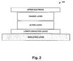
- FIG. 2illustrates another exemplary structure for a memory cell 200 in accordance with the present invention.
- a first or lower conductive layeris deposited on an upper surface of an insulating layer.
- the lower conductive layercan comprise aluminum, titanium, tungsten, platinum, palladium and their alloys and nitrides, conductive oxides and amorphous carbon (a-C).
- Such first or lower conductor layercan be about 1000 ⁇ -5000 ⁇ thick.
- Such active layercan comprise; polymer polyphenilacetylene+molecules of chloranil or tetracyano-quino-dimethane or dichlordicyanoquinone, (which can be deposited from solution by spin-coating); copper phthalocyanine (which can be deposited by thermal deposition method to about 30 ⁇ -1000 ⁇ ); copper hexadecafluoro phthalocyanine, amorphous carbon or palladium, (which can be deposited on the upper surface of the active layer by magnetron co-sputtering); porous silicon oxide (SiO 2 ) and polisilanes with N-carbazolylpropyl group; polymer polytiophene with cyclopentadienyl groups, (which can be deposited from solution by spin-coating; polisilanes with N-carbazolylpropyl group); polisilanes with cyclopentadienyl groups; polisilanes with amino groups; polytiophene with
- FIG. 3is a schematic diagram that illustrates an organic memory device 300 in various states in accordance with an aspect of the present invention.
- the device 300is depicted in a first “off” state 301 , an “on” state 302 , and a second “off” state 303 .
- memory devices formed in accordance with the present inventioncan have other states than those depicted in FIG. 3.
- the organic memory device 300comprises a top electrode 304 , a bottom electrode 306 and a selectively conductive layer 308 and at least one passive layer.
- various barrier layersfor example comprised of material such as Li 3 N, can be placed at various locations among the active layer, passive layer and electrodes.
- the electrons 310collect in the selectively conductive layer 308 near the bottom electrode 306 .
- the electrons 310are uniformly distributed thereby indicating an on state.
- the electronscollect in the selectively conductive layer 308 near the top electrode 304 .
- FIG. 4an array 400 of memory cells in accordance with an aspect of the present invention is illustrated.
- Such an arrayis generally formed on a silicon based wafer, and includes a plurality of columns 402 , referred to as bitlines, and a plurality of rows 404 , referred to as wordlines.
- bitlinesa plurality of columns 402
- wordlinesa plurality of rows 404
- Such bit line and wordlinescan be connected to the top and bottom metal layers of the memory component.
- the intersection of a bitline and a wordlineconstitutes the address of a particular memory cell.
- Datacan be stored in the memory cells (e.g., as a 0 or a 1) by choosing and sending signals to appropriate columns and rows in the array (e.g., via a column address strobe (CAS) 406 and a row address strobe (RAS) 408 , respectively).
- CAScolumn address strobe
- RASrow address strobe
- the state (e.g., a 0 or a 1) of the memory cell indicated at 410is a function of the 3 rd row and 8 th column of the array 400 .
- memory cellsinclude transistor-capacitor pairs.
- a chargecan be sent to the appropriate column (e.g., via CAS 406 ) to activate the respective transistors in the columns, and the state that respective capacitors should take on can be sent to the appropriate columns (e.g., via RAS 408 ).
- a sense-amplifiercan determine the level of charge on the capacitors. If it is more than 50 percent, it can be read as a 1; otherwise it can be read as a 0. It is to be appreciated that while the array 400 illustrated in FIG. 4 includes 64 memory cells (e.g., 8 rows ⁇ 8 columns), the present invention has application to any number of memory cells and is not to be limited to any particular configuration, arrangement and/or number of memory cells.
- FIG. 5a perspective diagram of an organic memory device in accordance with an aspect of the present invention is depicted.
- the memory deviceincludes a first electrode 504 , a passive layer 506 , an organic polymer layer 508 , and a second electrode 510 .
- the diagramalso illustrates a voltage source 502 connected to the first electrode 504 and the second electrode 510 that can apply an external stimulus in form of a voltage on the first electrode 504 and the second electrode 510 .
- the first electrode 504 and the second electrode 510are comprised of a conductive material, such as, aluminum, chromium, germanium, carbon, hafnium, indium, rhenium, ruthenium, tungsten, gold, magnesium, manganese, indium, iron, nickel, palladium, platinum, silver, titanium, zinc, alloys thereof, indium-tin oxide, polysilicon, doped amorphous silicon, metal carbides, nitrides and silicides, conducting oxides, semiconducting oxides, polysilicon, doped amorphous silicon, metal silicides, metal nitrides and silicides and the like.
- Exemplary alloys that can be utilized for the conductive materialinclude Hastelloy®, Kovar®, Invar, Monel®, Inconel®, stainless steel, magnesium-silver alloy, and various other alloys.
- an external stimulisuch as an applied electric field that exceeds a threshold value (“on” state)
- an applied voltage 502permits an applied voltage 502 to write, read, or erase information into/from the organic memory cell
- the absence of the external stimuli that exceeds a threshold value (“off” state)prevents an applied voltage to write or erase information into/from the organic memory cell.
- FIG. 6is a schematic diagram that depicts a passive layer 600 in accordance with an aspect of the present invention.
- a first layer 606is formed that forms the lower electrode.
- a second layer 604is formed on the first layer.
- the second layercomprises Cu x S and has a thickness of about 20 ⁇ or more.
- a third layer 602is formed on the second layer 604 .
- the third layer 602contains Cu 2 O, and/or CuO and generally has a thickness of about 10 ⁇ or less. It is appreciated that alternate aspects of the invention can employ suitable variations in composition and thickness and still be in accordance with the present invention.
- FIG. 7is a schematic diagram illustrating an organic layer 700 formed by a chemical vapor deposition (CVD) process as part of the active layer in accordance with an aspect of the present invention.
- the organic layer 700is formed via a gas phase reaction process.
- the organic layer 700is formed in contact with a passive layer and an electrode.
- the organic layer 700is comprised of polymer polydiphenylacetylene (pDPA). This polymer layer, as shown can be fabricated to be about 750 ⁇ thick.
- pDPApolymer polydiphenylacetylene
- FIG. 8a diagram depicting another organic layer 800 formed from a CVD process in accordance with an aspect of the present invention is illustrated.
- the organic layer 800is formed via a gas phase reaction process.
- the organic layer 800is formed in contact with a passive layer and an electrode.
- the organic polymer layer 800is comprised of polymer polyphenylacetylene (PPA).
- FIG. 9a block diagram of another organic layer 900 as part of the active layer of a memory cell formed by spin coating in accordance with an aspect of the present invention is illustrated.
- the organic layer 900is formed via a spin coating process, instead of a gas phase reaction process.
- the organic layer 900is formed in contact with a passive layer and an electrode.
- the organic layer 900is comprised substantially of PPA and has a thickness of about 1000 ⁇ .
- FIGS. 6 - 9various alternatives to and variations of the layers described in FIGS. 6 - 9 can be employed in accordance with the present invention.
- other methods of forming the active layercan be employed such as liquid phase reaction process, e.g. self assembling of an active layer(s) on bottom electrode (or a passive layer) via application of a suitable chemical compound.
- FIG. 10is a graph 1000 that illustrates an I-V graph for a memory device in accordance with an aspect of the present invention. It can be seen that from state 1, which indicates “off”, the device can be modified to be in state 2, which indicates “on”, by applying a positive voltage. Additionally, it can be seen that whilst in state 1, the organic memory device has a high impedance and low conductance. Subsequently, the device can be modified to change from state 2 to state 1 by application of a negative voltage, therein causing a reverse current until the state 1 is obtained.
- FIG. 11a three dimensional view of a memory device 1100 containing a plurality of memory cells with functional zones in accordance with an aspect of the invention is shown.
- the memory device 1100contains a plurality of first electrodes 1102 , a plurality of second electrodes 1104 , and a plurality of memory cell layers 1106 . Between the respective first and second electrodes are the controllably conductive media (not shown).
- the plurality of first electrodes 1102 and the plurality of second electrodes 1104are shown in substantially perpendicular orientation, although other orientations are possible.
- the three dimensional microelectronic memory deviceis capable of containing an extremely high number of memory cells thereby improving device density. Peripheral circuitry and devices are not shown for brevity.
- the memory cells/devicesare useful in any device requiring memory.
- the memory devicesare useful in computers, appliances, industrial equipment, hand-held devices, telecommunications equipment, medical equipment, research and development equipment, transportation vehicles, radar/satellite devices, and the like.
- Hand-held devices, and particularly hand-held electronic devicesachieve improvements in portability due to the small size and light weight of the memory devices. Examples of hand-held devices include cell phones and other two way communication devices, personal data assistants, palm pilots, pagers, notebook computers, remote controls, recorders (video and audio), radios, small televisions and web viewers, cameras, and the like.
- FIG. 12illustrates a methodology according to one aspect of the present invention.
- the exemplary methodis illustrated and described herein as a series of blocks representative of various events and/or acts, the present invention is not limited by the illustrated ordering of such blocks. For instance, some acts or events may occur in different orders and/or concurrently with other acts or events, apart from the ordering illustrated herein, in accordance with the invention. In addition, not all illustrated blocks, events or acts, may be required to implement a methodology in accordance with the present invention. Moreover, it will be appreciated that the exemplary method and other methods according to the invention may be implemented in association with a deposition and etch process for IC fabrication, and/or a damascene fill and polish procedure as well as in association with other systems and apparatus not illustrated or described.
- a bottom metal layeris being deposited, e.g., as part of an interconnect line as described in detail supra.
- a passive layeris formed over the bottom metal layer.
- an active layeris being deposited.
- a top metal layeris being formed over the active layer, e.g., as part of an interconnect line.
- layers of the memory componentcan be associated with and/or part of a memory cell or array, as described in more detail supra.
- a first or lower conductive conductoris deposited on an upper surface of an insulating layer.
- the first or lower conductormay be formed from materials selected from: aluminum, titanium, tungsten, platinum, palladium and their alloys and nitrides, conductive oxides and amorphous carbon (a-C).
- the first or lower conductor layeris about 3000 ⁇ thick.
- the active layeris mixture of a polymer polyphenylacetylene+molecules of chloraniline or tetracyano-quino-dimethane or dichlordicyanoquinone, which may be deposited from solution by spin-coating.
- the active layeris about 500 ⁇ thick.
- the second conductor layeris amorphous carbon or palladium, which can be deposited on the upper surface of the active layer by magnetron co-sputtering.
- the second conductor layeris about 2000 ⁇ thick.
- a first or lower conductive conductoris deposited on an upper surface of an insulating layer.
- the first or lower conductormay be formed from titanium and is about 3000 ⁇ thick.
- the lower active layeris copper phthalocyanine which can be deposited by thermal deposition method and is about 50 ⁇ thick.
- the upper active layeris copper hexadecafluoro phthalocyanine which can be deposited by thermal deposition method and is about 50 ⁇ thick.
- the second conductor layeris amorphous carbon, which can be deposited on the upper surface of the second polyaniline active layer by magnetron co-sputtering. The second conductor layer is about 2000 ⁇ thick.
- Ti/polysilanes with N-carbazolylpropyl group+silicon oxide (SiO 2 )/a-C or Pd or ITOThis cell is fabricated in a similar manner as Example I, except that the active layer is a composite of containing porous silicon oxide (SiO 2 ) and polysilanes with N-carbazolylpropyl group.
- a first or lower conductive conductoris deposited on an upper surface of an insulating layer.
- the first or lower conductormay be formed from materials selected from: aluminum, titanium, tungsten, platinum, palladium and their alloys and nitrides, conductive oxides, and amorphous carbon (a-C).
- the first or lower conductor layeris about 3000 ⁇ thick.
- the active layeris mixture of a polymer polythiophene with cyclopentadienyl groups, which may be deposited from solution by spin-coating.
- the active layeris about 500 ⁇ thick.
- the second conductor layeris amorphous carbon or palladium, which can be deposited on the upper surface of the active layer by magnetron co-sputtering.
- the second conductor layeris about 2000 ⁇ thick.
- Pd/polysilanes containing cyclopentadienyl groups/a-C or Pd or ITOThis cell is fabricated in a similar manner as Example 4, except that the active layer is polysilanes with cyclopentadienyl groups.
- Pd/polysilanes with amino groups/a-C or Pd or ITOThis cell is fabricated in a similar manner as Example 4, except that the active layer is polysilanes with amino groups.
Landscapes
- Engineering & Computer Science (AREA)
- Chemical & Material Sciences (AREA)
- Computer Hardware Design (AREA)
- Nanotechnology (AREA)
- Crystallography & Structural Chemistry (AREA)
- Theoretical Computer Science (AREA)
- Mathematical Physics (AREA)
- Physics & Mathematics (AREA)
- Manufacturing & Machinery (AREA)
- Materials Engineering (AREA)
- Semiconductor Memories (AREA)
- Nitrogen And Oxygen Or Sulfur-Condensed Heterocyclic Ring Systems (AREA)
- Read Only Memory (AREA)
Abstract
Description
- This application is a Continuation-in-Part of PCT application PCT/RU01/00334 filed Aug. 13, 2001.[0001]
- The present invention relates generally to memory devices and, in particular, to memory cells having functional layer(s) with a mechanism for electronic switching and resistance change, which is indicative of data storage.[0002]
- The volume, use and complexity of computers and electronic devices are continually increasing. Computers consistently become more powerful, new and improved electronic devices are continually developed (e.g., digital audio players, video players). Additionally, the growth and use of digital media (e.g., digital audio, video, images, and the like) have further pushed development of these devices. Such growth and development has vastly increased the amount of information desired/required to be stored and maintained for computer and electronic devices.[0003]
- Generally, information is stored and maintained in one or more of a number of types of storage devices. Storage devices include long term storage mediums such as, for example, hard disk drives, compact disk drives and corresponding media, digital video disk (DVD) drives, and the like. The long term storage mediums typically store larger amounts of information at a lower cost, but are slower than other types of storage devices. Storage devices also include memory devices, which are often, but not always, short term storage mediums. Memory devices tend to be substantially faster than long term storage mediums. Such memory devices include, for example, dynamic random access memory (DRAM), static random access memory (SRAM), double data rate memory (DDR), flash memory, read only memory (ROM), and the like. Memory devices are subdivided into volatile and non-volatile types. Volatile memory devices generally lose their information if they lose power and typically require periodic refresh cycles to maintain their information. Volatile memory devices include, for example, random access memory (RAM), DRAM, SRAM and the like. Non-volatile memory devices maintain their information whether or not power is maintained to the devices. Non-volatile memory devices include, but are not limited to, ROM, programmable read only memory (PROM), erasable programmable read only memory (EPROM), flash memory and the like. Volatile memory devices generally provide faster operation at a lower cost as compared to non-volatile memory devices.[0004]
- Memory devices generally include arrays of memory cells. Each memory cell can be accessed or “read”, “written”, and “erased” with information. The memory cells maintain information in an “off” or an “on” state (e.g., are limited to 2 states), also referred to as “0” and “1”. Typically, a memory device is addressed to retrieve a specified number of byte(s) (e.g., 8 memory cells per byte). For volatile memory devices, the memory cells must be periodically “refreshed” in order to maintain their state. Such memory devices are usually fabricated from semiconductor devices that perform these various functions and are capable of switching and maintaining the two states. The devices are often fabricated with inorganic solid state technology, such as, crystalline silicon devices. A common semiconductor device employed in memory devices is the metal oxide semiconductor field effect transistor (MOSFET).[0005]
- The use of portable computer and electronic devices has greatly increased demand for non-volatile memory devices. Digital cameras, digital audio players, personal digital assistants, and the like generally seek to employ large capacity non-volatile memory devices (e.g., flash memory, smart media, compact flash, and the like).[0006]
- Because of the increasing demand for information storage, memory device developers and manufacturers are constantly attempting to increase storage capacity for memory devices (e.g., increase storage per die or chip). A postage-stamp-sized piece of silicon may contain tens of millions of transistors, each transistor as small as a few hundred nanometers. However, silicon-based devices are approaching their fundamental physical size limits. Inorganic solid state devices are generally encumbered with a complex architecture which leads to high cost and a loss of data storage density. The volatile semiconductor memories based on inorganic semiconductor material must constantly be supplied with electric current with a resulting heating and high electric power consumption in order to maintain stored information. Non-volatile semiconductor devices have a reduced data rate and relatively high power consumption and large degree of complexity. Typically, fabrication processes for such cells are also not reliable.[0007]
- Therefore, there is a need to overcome the aforementioned deficiencies associated with conventional systems.[0008]
- The following presents a simplified summary of the invention in order to provide a basic understanding of one or more aspects of the invention. This summary is not an extensive overview of the invention. It is intended to neither identify key or critical elements of the invention, nor to delineate the scope of the present invention. Rather, the sole purpose of this summary is to present some concepts of the invention in a simplified form as a prelude to the more detailed description that is presented hereinafter.[0009]
- The present invention provided for systems and methods of fabricating semiconductor memory devices with a layered functional zone structure. Such functional layer facilitates migration of charges, (e.g. electrons, holes), and allows various impedance states for the memory cell. The layered structure can include selective conductive layers), active/passive layers, and barrier layers. Accordingly, a memory cell with a short resistance switch time and low operating voltages can be created, which is at the same time compatible with manufacturing methodologies for existing semiconductors.[0010]
- According to one aspect of the present invention a top and bottom electrode sandwich various film layers of functional or selective conductive, passive and active layers to form a memory cell. Such memory cell when subjected to an external stimulus, e.g. bias voltages, light radiation and the like, can be programmed (e.g. write/erase) via a desired impedance state induced in the memory cell. The desired impedance state represents one or more bits of information, and does not require a constant power supply or refresh cycles to maintain the desired information. Accordingly, the impedance state of the selectively conductive media can be read by applying a further external stimulus, such as an electric current. As with the written impedance state, the read impedance state represents one or more bits of information. Switching between the various states (e.g. read or write) can be a function of the electrical field created in such memory cell. In general, such formed electrical field can in turn be a function of the thickness of layers sandwiched between the top and bottom electrodes, and the applied electrical voltage between the first and second electrodes.[0011]
- According to another aspect of the present invention, a multi-cell memory component can be constructed having two or more non metal electrodes, e.g. amorphous carbon material, which sandwich therebetween the passive and the active layer. In addition, the active layer can comprise various types of conjugated polymers, such as redox-switchable molecular units. Under high external electrical field (e.g. 1-10V) electrons or holes can migrate from switchable molecular units to chains of the conjugated polymers. Such migration of charges can affect a conductivity of the material, and thus change a resistance of the memory cell. The state of the memory cell can then be read by applying a low external electrical voltage, (e.g. 0.05-0.1 V.)[0012]
- According to one aspect of the present invention, the passive layer can be deposited upon the lower electrode layer via vacuum thermal evaporation, sputtering, or plasma enhanced chemical vapor deposition (PECVD) utilizing a metal organic (MO) precursor. The deposition process can be monitored and controlled to facilitate, among other things, depositing the conductivity facilitating compound to a desired thickness.[0013]
- To the accomplishment of the foregoing and related ends, the invention, then, comprises the features hereinafter fully described. The following description and the annexed drawings set forth in detail certain illustrative aspects of the invention. However, these aspects are indicative of but a few of the various ways in which the principles of the invention may be employed. Other aspects, advantages and novel features of the invention will become apparent from the following detailed description of the invention when considered in conjunction with the drawings. To facilitate the reading of the drawings, some of the drawings may not have been drawn to scale from one figure to another or within a given figure.[0014]
- FIG. 1 is a schematic diagram illustrating a basic organic memory cell and its various sub layers in accordance with an aspect of the present invention.[0015]
- FIG. 2 is another schematic diagram of the organic memory cell with various active layers and sub layers.[0016]
- FIG. 3 is a schematic diagram depicting an organic memory device in various impedance states in accordance with an aspect of the present invention.[0017]
- FIG. 4 is a schematic block diagram illustrating multiple memory layer and memory cell storage and access in accordance with an aspect of the present invention.[0018]
- FIG. 5 is a perspective diagram of a memory device in accordance with an aspect of the present invention.[0019]
- FIG. 6 is a schematic diagram of a passive layer that can be employed in a memory device in accordance with an aspect of the present invention.[0020]
- FIG. 7 is a schematic diagram illustrating an organic polymer layer as part of an active layer formed by a CVD process in accordance with an aspect of the present invention.[0021]
- FIG. 8 is a schematic diagram illustrating another organic polymer layer formed by a CVD process in accordance with an aspect of the present invention.[0022]
- FIG. 9 is a schematic diagram of yet another organic polymer layer formed by a CVD process in accordance with an aspect of the present invention.[0023]
- FIG. 10 is a graph illustrating I-V characteristics for a memory device in accordance with an aspect of the present invention.[0024]
- FIG. 11 is a three dimensional view of a memory device having a functional layer in accordance with an aspect of the present invention.[0025]
- FIG. 12 illustrates a flow chart for a methodology according to the present invention.[0026]
- The present invention is now described with reference to the drawings, wherein like reference numerals are used to refer to like elements throughout. In the following description, for purposes of explanation, numerous specific details are set forth in order to provide a thorough understanding of the present invention. It may be evident, however, to one skilled in the art that one or more aspects of the present invention may be practiced with a lesser degree of these specific details. In other instances, known structures and devices may be shown in block diagram form in order to facilitate describing one or more aspects of the present invention.[0027]
- The invention is based on the problem of creating an essentially new type of memory cell which is capable of storing several bits of information, which has short resistance switch time and low operating voltages and at the same time allow to combine its manufacturing technology with that of the modern semiconductors.[0028]
- This problem is resolved as follows. The memory cell has a three-layer structure consisting of two electrodes with a functional zone between them. This is achieved by making the electrodes out of metallic and/or semiconductor and/or conductive polymer and/or optically transparent oxide or sulfide material, making the functional zone out of organic, metalorganic and non-organic materials, with different types of active elements built into the materials' molecular and/or crystalline structure, as well as by combining the materials with each other and/or with clusters based on them that change their; state, electrical charge and/or position under influence of an external electric field and/or light radiation.[0029]
- The described memory cell structure allows creating a memory element with single bit and multi-bit information writing, storing and reading methods. At the same time information is stored as the functional zone resistance value. For a memory cell with single bit storing mode the resistance value has two levels: high (e.g. representing 0) and low (e.g. representing I), while for a memory cell with multi-bit storing mode the resistance value has several levels corresponding to specific bits of information. For example, for a two-bit cell there are four levels of its resistance, for a four bit cell sixteen levels, and so forth. The memory cell is advantageously distinctive of the currently used elements in that it does not require non-interrupted power supply while storing information. The information storage time depends on the memory cell structure, on material used for the functional zone, and on recording mode. The time can vary from several seconds (can be used for dynamic memory) to several years (can be used for long term memory, such as Flash memory).[0030]
- The memory cell functional zone may contain an active layer based on organic and metalorganic conjugate polymers with active elements built into the main circuit and/or connected to the circuit or to the plane and/or built into the structure, with the elements forming or not forming a light emitting structure, or of an active layer based on organic, metalorganic and non-organic materials with instilled positive or negative ions, including molecular ions, and/or with instilled clusters based on solid electrolytes or with molecules and/or ions with an electric dipole element, and/or with clusters based on solid polymer and non-organic ferroelectrics, and/or with donor and acceptor molecules, and/or with organic and/or non-organic salts and/or acids and/or alkalis and/or water molecules which can dissociate in an electric field and/or under light radiation, and/or with non-organic and/or metalorganic and/or organic salts and/or molecules with variable valency of metals or atomic groups they contain. The described implementation of a functional zone allows to create a structure capable of changing the active layer resistance and/or forming high conductivity areas or lines in the active layer under external electric and/or light radiation effect on the memory cell and retaining this state for a long time without applying external electric fields.[0031]
- There are interesting prospects in implementing the functional zone as a multilayer structure containing several layers with various levels of activity, implemented, for example, out of organic, metalorganic and non-organic materials whose molecular and/or crystalline structure have instilled active elements based on them, which will change their state under electric field or light radiation influence, which allows to widen the range and quantity of electric resistance levels therefore increasing the memory data density.[0032]
- The functional zone may be implemented as a multilayer structure with alternating active, passive and barrier layers, where the passive layers are being made of organic, metalorganic and non-organic materials which are donor and/or acceptor charge carriers and possess ion and/or electron conductivity, while the barrier layer is made of material with high electron conductivity and low ion conductivity, which allows to improve the memory cell stability over time at the same time increasing data density due to increasing the quantity of the stored values of the memory cell electric resistance.[0033]
- The memory cell's electrode may be implemented in form of several separate elements, for example two or three elements placed above the functional layer, which permit more precise control the value of the cell electric resistance, therefore improving the quantity of information recording or the memory cell electric resistance analog values precision, as well as allows to decouple the information writing and reading electric circuits.[0034]
- The memory cell electrode may be implemented in the form of two elements separated in a space by a semiconductor and/or organic light emitting material and forming, for example, either a diode structure, or a photo resistance or a photo sensor element, which allows decoupling the information writing and reading electric circuits electrically or optically.[0035]
- The memory cell electrode may be implemented in the form of three parallel elements separated in space by a semiconductor and/or organic light emitting material and forming, for example, a light emitting structure and a photo resistance or a photo sensor element, which allows decoupling the information writing and reading electric circuits optically.[0036]
- FIG. 1 is a cross sectional illustration of a[0037]
memory cell 100, in accordance with an aspect of the present invention. Thememory cell 100 can be formed on a wafer, and typically on abase substrate 102, such as silicon. Thecell 100 includes abottom electrode 104, afunctional layer 103, and atop electrode 110. Unlike conventional inorganic memory cells that can maintain only two states, thememory cell 100 is capable of maintaining two or more states. Thus, a single cell of thememory cell 100 can hold one or more bits of information. Furthermore, thememory cell 100 is a non-volatile memory cell and consequently, does not require a constant or nearly constant power supply. - The[0038]
bottom electrode 104 is formed by depositing a first conductive material over thesubstrate 102. Trenches and/or vias can be formed in the substrate prior to deposition of such conductive material followed by selectively depositing the first conductive material into the trenches. According to one aspect of the present invention, theelectrodes electrodes electrodes - As illustrated in FIG. 1, sandwiched between the two[0039]
electrodes functional zone 103. Such functional zone can itself comprise of organic, metal organic, and non-organic materials, in the form of anactive layer 108 and apassive layer 106. - The[0040]
passive layer 106 is operative to transport charge from theelectrode 104 to the interface between theactive layer 108 and thepassive layer 106. Additionally, thepassive layer 106 facilitates charge carrier (e.g., electrons or holes) and/or metal ion injection into theactive layer 108 and increases the concentration of the charge carrier and/or metal ions in theactive layer 108 resulting in a modification of the conductivity of theactive layer 108. Furthermore, thepassive layer 106 can also store opposite charges in thepassive layer 106 in order to balance the total charge of thedevice 100. Both thepassive layer 106 and theactive layer 108 can comprise further sub layers, as shown in FIG. 1. - As further illustrated in FIG. 1, the[0041]
passive layer 106 can be part of thefunctional layer 103, which is formed on thebottom electrode 104. Thepassive layer 106 contains at least one conductivity facilitating compound that has the ability to donate and accept charges (holes and/or electrons). Generally, the conductivity facilitating compound has at least two relatively stable oxidation-reduction states that can permit the conductivity facilitating compound to donate and accept charges.Passive layer 106 should also be capable of donating and accepting ions. Examples of other conductivity facilitating compounds that can be employed for thepassive layer 106 include one or more of the following: tungsten oxide (WO3), molybdenum oxide (MoO3), titanium dioxide (TiO2), and the like. - The[0042]
passive layer 106 can in some instances act as a catalyst when forming theactive layer 108. In this connection, a backbone of a conjugated organic molecule can initially form adjacent thepassive layer 106, and grow or assemble away and substantially perpendicular to the passive layer surface. As a result, the backbones of the conjugated organic molecule can be self aligned in a direction that traverses the two electrodes. The passive layer can be formed by a deposition process (e.g. thermal deposition, PVD, non-selective CVD, and the like) or by a complete sulfidation of pre-deposited thin Cu layer. - Referring now to the[0043]
active layer 108, such layer can include various organic, metal organic conjugate polymers. In addition, various light emitting material, such as; light emitting structure, photo resistance, or photo sensors can be part of theactive layer 108. Moreover, additional material with donor/acceptor charges such as; molecules and/or ions with an electric dipole element, polymer ferroelectrics clusters, non-organic ferro-electrics, salts, alkalis and acids (organic or non organic), water molecules, materials with molecules that can dissociate in an electrical field and/or under radiation, organic salts and/or molecules with variable valency of metals, can also be employed as part of theactive layer 108. As such, examples of organic, non-organic salts, alkalis, acids and molecules that can dissociate in an electric field and/or under light radiation can include the following anions: I, Br, Cl, F, ClO4, AlCi4, PF6, AsF6, AsF4, SO3CF3, BF4, BCl4, NO3, POF4, CN, SiF3, SiF6, SO4, CH3CO2, C6H5CO2, CH3C6H4SO3, CF3SO3, N(SO3CF3)2, N(CF3SO2)(C4F9SO2), N(C4F9SO2)2, alkylphosphate, organoborate, bis-(4-nitrophenil)sulfonilimide, poly(styrene sulfonate)(polyanions)- and for cations such as: Li, Na, K, Rb, Cs, Ag, Ca, Mg, Zn, Fe, Cu, H, NH4and the like. Similarly, examples of clusters employed in theactive layer 108 that are based on polymer ferro electrics and non-organic ferro-electrics can include poly(vinylidene fluoride), poly(vinylidene fluoride)/trifluoroethylene, and the like. - In a related aspect of the present invention, various porous dielectric materials can also be employed as part of the[0044]
functional layer 103. Such porous material for example, can include matter selected from the group of Si, amorphous Si, silicon dioxide (SiO2), aluminum oxide (Al2O3), copper oxide (Cu2O), titanium dioxide (TiO2), boron nitride (BN), vanadium oxide (V2O3), carbon tri-nitride (CN3), and ferroelectric materials, including barium-strontium titanate ((Ba, Sr) TiO3). - In accordance with another aspect of the present invention, the[0045]
active layer 108 of thememory cell 100 can include polymers with variable electric conductivity. Such polymers with variable electrical conductivity can include; polydiphenylacetylene, poly(t-butyl)diphenylacetylene, poly(trifluoromethyl)diphenylacetylene, polybis-trifluoromethyl)acetylene, polybis(t-butyidiphenyl)acetylene, poly(trimethylsilyl) diphenylacetylene, poly(carbazole)diphenylacetylene, polydiacetylene, polyphenylacetylene, polypyridineacetylene, polymethoxyphenylacetylene, polymethylphenylacetylene, poly(t-butyl)phenylacetylene, polynitro-phenylacetylene, poly(trifluoromethyl)phenylacetylene, poly(trimethylsilyl)pheylacetylene, polydipyrrylmethane, polyindoqiunone, polydihydroxyindole, polytrihydroxyindole, furane-polydihydroxyindole, polyindoqiunone-2-carboxyl, polyindoqiunone monohydrate, polybenzobisthiazole, poly(p-phenylene sulfide) and derivatives with active molecular group. - As used in this application, an active molecule or molecular group can be one that changes a property when subjected to an electrical field or light radiation, (e.g. iozinable group); such as: nitro group, amino group, cyclopentadienyl, dithiolane, metilcyclopentadienyl, fulvalenediyl, indenyl, fluorenyl, cyclobis(paraquart-p-phenylene), bipyridinium, phenothiazine, diazapyrenium, benzonitrile, benzonate, benzamide, carbazole, dibenzothiophene, nitrobenzene, aminobenzenesulfonate, amonobenzanate, and molecular units with redox-active metals; metallocenes (Fe, V, Cr, Co, Ni and the like) complex, polypyridine metal complex (Ru, Os and the like).[0046]
- In another aspect of the present invention, the[0047]
active layer 108 can include polymers such as polyaniline, polythiophene, polypyrrole, polysilane, polystyrene, polyfuran, polyindole, polyazulene, polyphenylene, polypyridine, polybipyridine, polyphthalocyanine, polysexithiofene, poly(siliconoxohemiporphyrazine), poly(germaniumoxohemiporphyrazine), poly(ethylenedioxythiophene) and related derivatives with active molecular group. It is to be appreciated that other suitable and related chemical compounds can also be employed including: aromatic hydrocarbons; organic molecules with donor and acceptor properties (N-Ethylcarbazole, tetrathiotetracene, tetrathiofulvalene, tetracyanoquinodimethane, tetracyanoethylene, cloranol, dinitro-n phenyl and so on); metallo-organic complexes (bisdiphenylglyoxime, bisorthophenylenediimine, tetraaza-tetramethylannulene and so on); porphyrin, phthalocyanine, hexadecafluoro phthalocyanine and their derivatives with active molecular group. - In general, the[0048]
memory cell structure 100 employing the material discussed supra can exhibit a formation of high conductivity areas, or affect a resistance of thefunctional zone 103 in response to an external stimulus such as an electric voltage, electric current, light radiation, and the like. For example, presence of ferro-electric material can increase an internal electric field intensity, and as a result application of a lower external electric voltage can be required for a writing of thememory cell 100. As explained supia, theactive layer 108 can be created on thepassive layer 106 and results in an interface between the two layers. Moreover, theactive layer 108 can be formed via a number of suitable techniques. One such technique involves growing theactive layer 108 in the form of an organic layer from thepassive layer 106. Another technique that can be utilized is a spin-on technique which involves depositing a mixture of the material and a solvent, and then removing the solvent from the substrate/electrode. Another suitable technique is chemical vapor deposition (CVD). CVD includes low pressure chemical vapor deposition (LPCVD), plasma enhanced chemical vapor deposition (PECVD), and high density chemical vapor deposition (HDCVD). It is not typically necessary to functionalize one or more ends of the organic molecule in order to attach it to an electrode/passive layer. Sometime it may have a chemical bond formed between the conjugated organic polymer of theactive layer 108 and thepassive layer 106. - In one aspect of the present invention, the[0049]
active layer 108 can also be comprised of a conjugated organic material, such as a small organic molecule and a conjugated polymer. If the organic layer is polymer, a polymer backbone of the conjugated organic polymer may extend lengthwise between theelectrodes 104 and110 (e.g., generally substantially perpendicular to the inner, facing surfaces of theelectrodes 104 and110). The conjugated organic molecule can be linear or branched such that the backbone retains its conjugated nature. Such conjugated molecules are characterized in that they have overlapping π orbitals and that they can assume two or more resonant structures. The conjugated nature of the conjugated organic materials contributes to the controllably conductive properties of the selectively conductive media. - In this connection, the conjugated organic material of the[0050]
active layer 108 has the ability to donate and accept charges (holes and/or electrons). Generally, the conjugated organic molecule has at least two relatively stable oxidation-reduction states. The two relatively stable states permit the conjugated organic polymer to donate and accept charges and electrically interact with the conductivity facilitating compound. - The organic material employed as part of the[0051]
active layer 108 according to one aspect of the present invention can be cyclic or acyclic. For some cases, such as organic polymers, the organic material can self assemble on bottom electrode during formation or deposition. Examples of conjugated organic polymers include one or more of polyacetylene (cis or trans); polyphenylacetylene (cis or trans); polydiphenylacetylene; polyaniline; poly(p-phenylene vinylene); polythiophene; polyporphyrins; porphyrinic macrocycles, thiol derivatized polyporphyrins; poly(p-phenylene)s; poly(imide)s; polymetallocenes such as polyferrocenes, polyphthalocyanines; polyvinylenes; polystiroles; and the like. Additionally, the properties of the organic material can be modified by doping with a suitable dopant. - The[0052]
top electrode 110 is formed on/over the organic material of theactive layer 108 and/or thepassive layer 106. Thetop electrode 110 can be comprised of similar material as described supra for thelower electrode 104. Additionally, alloys with phosphorous, nitrogen, carbon, and boron, graphite, conductive oxides and other conductive substances can also be employed. - The thickness of the[0053]
bottom electrode 104 and thetop electrode 110 can vary depending on the implementation and the memory cell being constructed. However, some exemplary thickness ranges include about 0.01 μm or more and about 10 μm or less, about 0.05 μm or more and about 5 μm or less, and/or about 0.1 μm or more and about 1 μm or less. - The[0054]
active layer 108 and thepassive layer 106 can be collectively referred to as a selectively conductive media or a selectively conductive layer, which is a part of thefunctional zone 103. The conductive properties of this media (e.g., conductive, non-conductive, semi-conductive) can be modified in a controlled manner by applying various voltages across the media via theelectrodes - The organic layer that in one exemplary aspect can form the[0055]
active layer 108, has a suitable thickness that depends upon the chosen implementations and/or the memory cell being fabricated. Some suitable exemplary ranges of thickness for the organic polymer layer, which in part can form theactive layer 108, are about 0.001 μm or more and about 5 μm or less, about 0.01 μm or more and about 2.5 μm or less, and about a thickness of about 0.05 μm or more and about 1 μm or less. Similarly, thepassive layer 106 has a suitable thickness that can vary based on the implementation and/or memory cell being fabricated. Some examples of suitable thicknesses for thepassive layer 106 are as follows: a thickness of about 2 Å or more and about 0.1 μm or less, a thickness of about 10 Å or more and about 0.01 μm or less, and a thickness of about 50 Å or more and about 0.005 μm or less. - In order to facilitate operation of the[0056]
memory cell 100, theactive layer 108 is generally thicker than thepassive layer 106. In one aspect, the thickness of the active layer is from about 0.1 to about 500 times greater than the thickness of the passive layer. It is appreciated that other suitable ratios can be employed in accordance with the present invention. It is to be appreciated that the various layers employed in fabricating the memory cell can themselves comprise a plurality of sub layers, as depicted in FIG. 1 whereinpassive layer 106, andactive layer 108, are each shown as comprising three sub-layers. - The[0057]
memory cell 100, like conventional memory cells, can have two states, a conductive (low impedance or “on”) state or non-conductive (high impedance or “off”) state. However, unlike conventional memory cells, thememory cell 100 is able to have/maintain a plurality of states, in contrast to a conventional memory cell that is limited to two states (e.g., off or on). The memory cell can employ varying degrees of conductivity to identify additional states. For example, thememory cell 100 can have a low impedance state, such as a very highly conductive state (very low impedance state), a highly conductive state (low impedance state), a conductive state (medium level impedance state), and a non-conductive state (high impedance state) thereby enabling the storage of multiple bits of information in a single organic memory cell, such as 2 or more bits of information or 4 or more bits of information (e.g., 4 states providing 2 bits of information, 8 states providing 3 bits of information, and the like.) Switching thememory cell 100 to a particular state is referred to as programming or writing. Programming is accomplished by applying a particular voltage (e.g., 9 volts, 2 volts, 1 volt, . . . ) across the selectively conductive media via theelectrodes memory cell 100, the thickness of the various layers, and the like. Generally speaking, the presence of an external stimuli such as an applied electric field that exceeds a threshold value (“on” state) permits an applied voltage to write, read, or erase information into/from thememory cell 100; whereas the absence of the external stimuli that exceeds a threshold value (“off” state) prevents an applied voltage to write or erase information into/from thememory cell 100. - To read information from the memory device, a voltage or electric field (e.g., 2 volts, 1 volt, 0.5 volts) is applied via a voltage source. Then, an impedance measurement is performed which, therein determines which operating state the memory device is in (e.g., high impedance, very low impedance, low impedance, medium impedance, and the like). As stated supra, the impedance relates to, for example, “on” (e.g., I) or “off” (e.g., 0) for a dual state device or to “00”, “01”, “10”, or “11” for a quad state device. It is appreciated that other numbers of states can provide other binary interpretations. To erase information written into the organic memory device, a negative voltage or a polarity opposite the polarity of the writing signal that exceeds a threshold value is applied.[0058]
- FIG. 2 illustrates another exemplary structure for a[0059]
memory cell 200 in accordance with the present invention. A first or lower conductive layer is deposited on an upper surface of an insulating layer. The lower conductive layer can comprise aluminum, titanium, tungsten, platinum, palladium and their alloys and nitrides, conductive oxides and amorphous carbon (a-C). Such first or lower conductor layer can be about 1000 Å-5000 Å thick. Upon this lower conductive and active layer is deposited. Such active layer can comprise; polymer polyphenilacetylene+molecules of chloranil or tetracyano-quino-dimethane or dichlordicyanoquinone, (which can be deposited from solution by spin-coating); copper phthalocyanine (which can be deposited by thermal deposition method to about 30 Å-1000 Å); copper hexadecafluoro phthalocyanine, amorphous carbon or palladium, (which can be deposited on the upper surface of the active layer by magnetron co-sputtering); porous silicon oxide (SiO2) and polisilanes with N-carbazolylpropyl group; polymer polytiophene with cyclopentadienyl groups, (which can be deposited from solution by spin-coating; polisilanes with N-carbazolylpropyl group); polisilanes with cyclopentadienyl groups; polisilanes with amino groups; polytiophene with alkyl amino groups; polytiophene with cyclopentadienyl alkyl groups; composite containing polydiphenilacetylene containing carbazolyl groups and dinitro-n-phenyl (DNP); polyethylenedioxythiophene and Li CF3SO3salt containing porous ferroelectric (polyvinyline fluoride), polydiphenilacetylene containing carbazolyl groups dinitro-n-phenyl (DNP); polyethylenedioxythiophene and salt of potassium hexycyanoferrate. - FIG. 3 is a schematic diagram that illustrates an[0060]
organic memory device 300 in various states in accordance with an aspect of the present invention. Thedevice 300 is depicted in a first “off”state 301, an “on”state 302, and a second “off”state 303. It is appreciated that memory devices formed in accordance with the present invention can have other states than those depicted in FIG. 3. Theorganic memory device 300 comprises atop electrode 304, abottom electrode 306 and a selectivelyconductive layer 308 and at least one passive layer. In addition, various barrier layers, for example comprised of material such as Li3N, can be placed at various locations among the active layer, passive layer and electrodes. In the firstoff state 301,electrons 310 collect in the selectivelyconductive layer 308 near thebottom electrode 306. In the onstate 302, theelectrons 310 are uniformly distributed thereby indicating an on state. In the secondoff state 303, the electrons collect in the selectivelyconductive layer 308 near thetop electrode 304. - Turning to FIG. 4, an[0061]
array 400 of memory cells in accordance with an aspect of the present invention is illustrated. Such an array is generally formed on a silicon based wafer, and includes a plurality ofcolumns 402, referred to as bitlines, and a plurality ofrows 404, referred to as wordlines. Such bit line and wordlines can be connected to the top and bottom metal layers of the memory component. The intersection of a bitline and a wordline constitutes the address of a particular memory cell. Data can be stored in the memory cells (e.g., as a 0 or a 1) by choosing and sending signals to appropriate columns and rows in the array (e.g., via a column address strobe (CAS)406 and a row address strobe (RAS)408, respectively). For example, the state (e.g., a 0 or a 1) of the memory cell indicated at410 is a function of the 3rdrow and 8thcolumn of thearray 400. In dynamic random access memory (DRAM), for example, memory cells include transistor-capacitor pairs. To write to a memory cell, a charge can be sent to the appropriate column (e.g., via CAS406) to activate the respective transistors in the columns, and the state that respective capacitors should take on can be sent to the appropriate columns (e.g., via RAS408). To read the state of the cells, a sense-amplifier can determine the level of charge on the capacitors. If it is more than 50 percent, it can be read as a 1; otherwise it can be read as a 0. It is to be appreciated that while thearray 400 illustrated in FIG. 4 includes 64 memory cells (e.g., 8 rows×8 columns), the present invention has application to any number of memory cells and is not to be limited to any particular configuration, arrangement and/or number of memory cells. - Now referring to FIG. 5, a perspective diagram of an organic memory device in accordance with an aspect of the present invention is depicted. The memory device includes a[0062]
first electrode 504, apassive layer 506, anorganic polymer layer 508, and asecond electrode 510. The diagram also illustrates avoltage source 502 connected to thefirst electrode 504 and thesecond electrode 510 that can apply an external stimulus in form of a voltage on thefirst electrode 504 and thesecond electrode 510. - The[0063]
first electrode 504 and thesecond electrode 510 are comprised of a conductive material, such as, aluminum, chromium, germanium, carbon, hafnium, indium, rhenium, ruthenium, tungsten, gold, magnesium, manganese, indium, iron, nickel, palladium, platinum, silver, titanium, zinc, alloys thereof, indium-tin oxide, polysilicon, doped amorphous silicon, metal carbides, nitrides and silicides, conducting oxides, semiconducting oxides, polysilicon, doped amorphous silicon, metal silicides, metal nitrides and silicides and the like. Exemplary alloys that can be utilized for the conductive material include Hastelloy®, Kovar®, Invar, Monel®, Inconel®, stainless steel, magnesium-silver alloy, and various other alloys. - As explained supra, the presence of an external stimuli; such as an applied electric field that exceeds a threshold value (“on” state), permits an applied[0064]
voltage 502 to write, read, or erase information into/from the organic memory cell; whereas the absence of the external stimuli that exceeds a threshold value (“off” state) prevents an applied voltage to write or erase information into/from the organic memory cell. - FIG. 6 is a schematic diagram that depicts a[0065]
passive layer 600 in accordance with an aspect of the present invention. Afirst layer 606 is formed that forms the lower electrode. Asecond layer 604 is formed on the first layer. The second layer comprises CuxS and has a thickness of about 20 Å or more. Athird layer 602 is formed on thesecond layer 604. Thethird layer 602 contains Cu2O, and/or CuO and generally has a thickness of about 10 Å or less. It is appreciated that alternate aspects of the invention can employ suitable variations in composition and thickness and still be in accordance with the present invention. - FIG. 7 is a schematic diagram illustrating an[0066]
organic layer 700 formed by a chemical vapor deposition (CVD) process as part of the active layer in accordance with an aspect of the present invention. Theorganic layer 700 is formed via a gas phase reaction process. Typically, theorganic layer 700 is formed in contact with a passive layer and an electrode. Theorganic layer 700 is comprised of polymer polydiphenylacetylene (pDPA). This polymer layer, as shown can be fabricated to be about 750 Å thick. - Turning now to FIG. 8, a diagram depicting another[0067]
organic layer 800 formed from a CVD process in accordance with an aspect of the present invention is illustrated. Once again, theorganic layer 800 is formed via a gas phase reaction process. Theorganic layer 800 is formed in contact with a passive layer and an electrode. Theorganic polymer layer 800 is comprised of polymer polyphenylacetylene (PPA). - Referring to FIG. 9, a block diagram of another[0068]
organic layer 900 as part of the active layer of a memory cell formed by spin coating in accordance with an aspect of the present invention is illustrated. Theorganic layer 900 is formed via a spin coating process, instead of a gas phase reaction process. Theorganic layer 900 is formed in contact with a passive layer and an electrode. Theorganic layer 900 is comprised substantially of PPA and has a thickness of about 1000 Å. - Experimental results tend to show that organic layers formed via spin coating yield a more reliable polymer layer than polymer layers formed via CVD. This may be due to the presence of oxygen and lack of control of heat generated by polymerization under CVD. It is appreciated that controlling heat and oxygen during polymerization for CVD processes can improve the resulting polymer layer.[0069]
- It is appreciated that various alternatives to and variations of the layers described in FIGS.[0070]6-9 can be employed in accordance with the present invention. Moreover, it is to be appreciated that other methods of forming the active layer can be employed such as liquid phase reaction process, e.g. self assembling of an active layer(s) on bottom electrode (or a passive layer) via application of a suitable chemical compound.
- FIG. 10 is a graph[0071]1000 that illustrates an I-V graph for a memory device in accordance with an aspect of the present invention. It can be seen that from
state 1, which indicates “off”, the device can be modified to be instate 2, which indicates “on”, by applying a positive voltage. Additionally, it can be seen that whilst instate 1, the organic memory device has a high impedance and low conductance. Subsequently, the device can be modified to change fromstate 2 tostate 1 by application of a negative voltage, therein causing a reverse current until thestate 1 is obtained. - Referring to FIG. 11, a three dimensional view of a[0072]
memory device 1100 containing a plurality of memory cells with functional zones in accordance with an aspect of the invention is shown. Thememory device 1100 contains a plurality offirst electrodes 1102, a plurality ofsecond electrodes 1104, and a plurality of memory cell layers1106. Between the respective first and second electrodes are the controllably conductive media (not shown). The plurality offirst electrodes 1102 and the plurality ofsecond electrodes 1104 are shown in substantially perpendicular orientation, although other orientations are possible. The three dimensional microelectronic memory device is capable of containing an extremely high number of memory cells thereby improving device density. Peripheral circuitry and devices are not shown for brevity. - The memory cells/devices are useful in any device requiring memory. For example, the memory devices are useful in computers, appliances, industrial equipment, hand-held devices, telecommunications equipment, medical equipment, research and development equipment, transportation vehicles, radar/satellite devices, and the like. Hand-held devices, and particularly hand-held electronic devices, achieve improvements in portability due to the small size and light weight of the memory devices. Examples of hand-held devices include cell phones and other two way communication devices, personal data assistants, palm pilots, pagers, notebook computers, remote controls, recorders (video and audio), radios, small televisions and web viewers, cameras, and the like.[0073]
- FIG. 12 illustrates a methodology according to one aspect of the present invention.[0074]
- While the exemplary method is illustrated and described herein as a series of blocks representative of various events and/or acts, the present invention is not limited by the illustrated ordering of such blocks. For instance, some acts or events may occur in different orders and/or concurrently with other acts or events, apart from the ordering illustrated herein, in accordance with the invention. In addition, not all illustrated blocks, events or acts, may be required to implement a methodology in accordance with the present invention. Moreover, it will be appreciated that the exemplary method and other methods according to the invention may be implemented in association with a deposition and etch process for IC fabrication, and/or a damascene fill and polish procedure as well as in association with other systems and apparatus not illustrated or described.[0075]
- Initially, at[0076]1202 a bottom metal layer is being deposited, e.g., as part of an interconnect line as described in detail supra. Next at1204 a passive layer, as discussed in detail supra, is formed over the bottom metal layer. At1206, and over the passive layer, an active layer is being deposited. Next and at1208, a top metal layer is being formed over the active layer, e.g., as part of an interconnect line. In addition, layers of the memory component can be associated with and/or part of a memory cell or array, as described in more detail supra.
- The following examples illustrate various particular aspects of the present invention. Unless otherwise indicated in the following examples and elsewhere in the specification and claims, all parts and percentages are by weight, all temperatures are in degrees Centigrade, and pressure is at or near atmospheric pressure.[0077]
- Ti/polyphenylacetylene+molecules of chloraniline or tetracyano-quino-dimethane/amorphous carbon (a-C). A first or lower conductive conductor is deposited on an upper surface of an insulating layer. The first or lower conductor may be formed from materials selected from: aluminum, titanium, tungsten, platinum, palladium and their alloys and nitrides, conductive oxides and amorphous carbon (a-C). The first or lower conductor layer is about 3000 Å thick. The active layer is mixture of a polymer polyphenylacetylene+molecules of chloraniline or tetracyano-quino-dimethane or dichlordicyanoquinone, which may be deposited from solution by spin-coating. The active layer is about 500 Å thick. The second conductor layer is amorphous carbon or palladium, which can be deposited on the upper surface of the active layer by magnetron co-sputtering. The second conductor layer is about 2000 Å thick.[0078]
- Ti/copper phthalocyanine/cupper hexadecafluoro phthalocyanine/a-C or Pd or ITO. A first or lower conductive conductor is deposited on an upper surface of an insulating layer. The first or lower conductor may be formed from titanium and is about 3000 Å thick. The lower active layer is copper phthalocyanine which can be deposited by thermal deposition method and is about 50 Å thick. The upper active layer is copper hexadecafluoro phthalocyanine which can be deposited by thermal deposition method and is about 50 Å thick. The second conductor layer is amorphous carbon, which can be deposited on the upper surface of the second polyaniline active layer by magnetron co-sputtering. The second conductor layer is about 2000 Å thick.[0079]
- Ti/polysilanes with N-carbazolylpropyl group+silicon oxide (SiO[0080]2)/a-C or Pd or ITO. This cell is fabricated in a similar manner as Example I, except that the active layer is a composite of containing porous silicon oxide (SiO2) and polysilanes with N-carbazolylpropyl group.
- Ti/Polythiophene with cyclopentadienyl groups/amorphous carbon (a-C). A first or lower conductive conductor is deposited on an upper surface of an insulating layer. The first or lower conductor may be formed from materials selected from: aluminum, titanium, tungsten, platinum, palladium and their alloys and nitrides, conductive oxides, and amorphous carbon (a-C). The first or lower conductor layer is about 3000 Å thick. The active layer is mixture of a polymer polythiophene with cyclopentadienyl groups, which may be deposited from solution by spin-coating. The active layer is about 500 Å thick. The second conductor layer is amorphous carbon or palladium, which can be deposited on the upper surface of the active layer by magnetron co-sputtering. The second conductor layer is about 2000 Å thick.[0081]
- Ti/polysilanes with N-carbazolylpropyl group/a-C or Pd or ITO. This cell is fabricated in a similar manner as Example 4, except that the active layer is polysilanes with N-carbazolylpropyl group.[0082]
- Pd/polysilanes containing cyclopentadienyl groups/a-C or Pd or ITO. This cell is fabricated in a similar manner as Example 4, except that the active layer is polysilanes with cyclopentadienyl groups.[0083]
- Pd/polysilanes with amino groups/a-C or Pd or ITO. This cell is fabricated in a similar manner as Example 4, except that the active layer is polysilanes with amino groups.[0084]
- Ti/Polythiophene with amino groups/a-C or Pd or ITO. This cell is fabricated in a similar manner as Example 4, except that the active layer is polythiophene with amino groups.[0085]
- Ti/Polythiophene with alkyl amino groups/a-C or Pd or ITO. This cell is fabricated in a similar manner as Example 4, except that the active layer is polythiophene with alkyl amino groups.[0086]
- Ti/Polythiophene with cyclopentadienyl alkyl groups/a-C or Pd or ITO. This cell is fabricated in a similar manner as Example 4, except that the active layer is polythiophene with cyclopentadienyl alkyl groups.[0087]
- Ti/Polythiophene with cyclopentadienyl groups/a-C or Pd or ITO. This cell is fabricated in a similar manner as Example 4, except that the active layer is polythiophene with cyclopentadienyl alkyl groups.[0088]
- Ti/Polydiphenilacetylene with carbazolyl groups+dinitro-n-phenyl (DNP)/a-C. This cell was fabricated in a similar manner as Example 4, except that the active layer is a composite containing polydiphenilacetylene containing carbazolyl groups and dinitro-n-phenyl(DNP).[0089]
- Ti/polyethylenedioxythiophene+Li CF[0090]3SO3/Pd. This cell is fabricated in a similar manner as Example 4, except that the active layer is a composite of containing polyethylenedioxythiophene and LiCF3SO3salt.
- Ti/polydiphenylacetylene containing carbazolyl groups+dinitro-n-phenyl (DNP)+porous ferroelectric (polyvinyline fluoride)/a-C. This cell is fabricated in a similar manner as Example 4, except that the active layer is a composite of containing porous ferroelectric (polyvinyline fluoride), polydiphenylacetylene containing carbazolyl groups and dinitro-n-phenyl(DNP).[0091]
- Ti/polyethylenedioxythiophene+salt of potassium hexycyanoferrate/Pd. This cell is fabricated in a similar manner as Example 4, except that the active layer is a composite of containing polyethylenedioxythiophene and salt of potassium hexycyanoferrate.[0092]
- Although the invention has been shown and described with respect to certain illustrated aspects, it will be appreciated that equivalent alterations and modifications will occur to others skilled in the art upon the reading and understanding of this specification and the annexed drawings. In particular regard to the various functions performed by the above described components (assemblies, devices, circuits, systems, etc.), the terms (including a reference to a “means”) used to describe such components are intended to correspond, unless otherwise indicated, to any component which performs the specified function of the described component (e.g., that is functionally equivalent), even though not structurally equivalent to the disclosed structure, which performs the function in the herein illustrated exemplary aspects of the invention. In this regard, it will also be recognized that the invention includes a system as well as a computer-readable medium having computer-executable instructions for performing the acts and/or events of the various methods of the invention.[0093]
- In addition, while a particular feature of the invention may have been disclosed with respect to only one of several implementations, such feature may be combined with one or more other features of the other implementations as may be desired and advantageous for any given or particular application. Furthermore, to the extent that the terms “includes”, “including”, “has”, “having”, and variants thereof are used in either the detailed description or the claims, these terms are intended to be inclusive in a manner similar to the term “comprising”.[0094]
Claims (32)
Applications Claiming Priority (1)
| Application Number | Priority Date | Filing Date | Title |
|---|---|---|---|
| PCT/RU2001/000334WO2003017282A1 (en) | 2001-08-13 | 2001-08-13 | Memory cell |
Related Parent Applications (1)
| Application Number | Title | Priority Date | Filing Date |
|---|---|---|---|
| PCT/RU2001/000334Continuation-In-PartWO2003017282A1 (en) | 2001-08-13 | 2001-08-13 | Memory cell |
Publications (2)
| Publication Number | Publication Date |
|---|---|
| US20040159835A1true US20040159835A1 (en) | 2004-08-19 |
| US7026702B2 US7026702B2 (en) | 2006-04-11 |
Family
ID=20129643
Family Applications (5)
| Application Number | Title | Priority Date | Filing Date |
|---|---|---|---|
| US10/486,864Expired - LifetimeUS6992323B2 (en) | 2001-08-13 | 2001-08-13 | Memory cell |
| US10/238,880Expired - LifetimeUS6815286B2 (en) | 2001-08-13 | 2002-09-11 | Memory device |
| US10/414,353Expired - LifetimeUS6864522B2 (en) | 2001-08-13 | 2003-04-15 | Memory device |
| US10/776,850Expired - Fee RelatedUS7026702B2 (en) | 2001-08-13 | 2004-02-11 | Memory device |
| US10/776,870Expired - Fee RelatedUS7254053B2 (en) | 2001-08-13 | 2004-02-11 | Active programming and operation of a memory device |
Family Applications Before (3)
| Application Number | Title | Priority Date | Filing Date |
|---|---|---|---|
| US10/486,864Expired - LifetimeUS6992323B2 (en) | 2001-08-13 | 2001-08-13 | Memory cell |
| US10/238,880Expired - LifetimeUS6815286B2 (en) | 2001-08-13 | 2002-09-11 | Memory device |
| US10/414,353Expired - LifetimeUS6864522B2 (en) | 2001-08-13 | 2003-04-15 | Memory device |
Family Applications After (1)
| Application Number | Title | Priority Date | Filing Date |
|---|---|---|---|
| US10/776,870Expired - Fee RelatedUS7254053B2 (en) | 2001-08-13 | 2004-02-11 | Active programming and operation of a memory device |
Country Status (8)
| Country | Link |
|---|---|
| US (5) | US6992323B2 (en) |
| EP (1) | EP1434232B1 (en) |
| JP (1) | JP2005500682A (en) |
| KR (1) | KR100860134B1 (en) |
| CN (1) | CN100419906C (en) |
| BR (1) | BR0117103A (en) |
| DE (1) | DE60130586T2 (en) |
| WO (1) | WO2003017282A1 (en) |
Cited By (92)
| Publication number | Priority date | Publication date | Assignee | Title |
|---|---|---|---|---|
| US20040245517A1 (en)* | 2003-06-03 | 2004-12-09 | Campbell Kristy A. | Diode/superionic conductor/polymer memory structure |
| US20050006640A1 (en)* | 2003-06-26 | 2005-01-13 | Jackson Warren B. | Polymer-based memory element |
| US20050058009A1 (en)* | 2003-09-03 | 2005-03-17 | Yang Yang | Memory devices based on electric field programmable films |
| US20050202620A1 (en)* | 2004-03-10 | 2005-09-15 | Campbell Kristy A. | Method to manufacture polymer memory with copper ion switching species |
| US20050227377A1 (en)* | 2004-03-31 | 2005-10-13 | Renavikar Mukul P | Creation of electron traps in metal nitride and metal oxide electrodes in polymer memory devices |
| US20050270442A1 (en)* | 2004-05-20 | 2005-12-08 | Yang Yang | Nanoparticle-polymer bistable devices |
| US20060002168A1 (en)* | 2004-07-01 | 2006-01-05 | Krieger Juri H | Switchable memory diode - a new memory device |
| DE102004046392A1 (en)* | 2004-09-24 | 2006-04-06 | Infineon Technologies Ag | Semiconductor memory |
| US20060098472A1 (en)* | 2004-11-10 | 2006-05-11 | Seung-Eon Ahn | Nonvolatile memory device, array of nonvolatile memory devices, and methods of making the same |
| US20060103026A1 (en)* | 2004-07-27 | 2006-05-18 | Campbell Kristy A | Amorphous carbon-based non-volatile memory |
| US20060131560A1 (en)* | 2003-02-03 | 2006-06-22 | The Regents Of The University Of California | Rewritable nano-surface organic electrical bistable devices |
| US20070009821A1 (en)* | 2005-07-08 | 2007-01-11 | Charlotte Cutler | Devices containing multi-bit data |
| US20070069246A1 (en)* | 2005-09-23 | 2007-03-29 | Norbert Koch | Hybrid devices |
| US7208757B1 (en)* | 2004-12-23 | 2007-04-24 | Spansion Llc | Memory element with nitrogen-containing active layer |
| US20070090343A1 (en)* | 2005-10-21 | 2007-04-26 | Spansion Llc | System and method for processing an organic memory cell |
| US20070117256A1 (en)* | 2005-11-23 | 2007-05-24 | Duncan Stewart | Control layer for a nanoscale electronic switching device |
| US20070164272A1 (en)* | 2003-12-03 | 2007-07-19 | Yang Yang | Three-terminal electrical bistable devices |
| US20070176172A1 (en)* | 2006-02-02 | 2007-08-02 | Won Jae Joo | Organic memory devices and methods of fabricating such devices |
| US20070176173A1 (en)* | 2005-12-23 | 2007-08-02 | Ramakrishnan Ed S | Electronic device including an organic active layer and process for forming the electronic device |
| US7273766B1 (en)* | 2005-01-12 | 2007-09-25 | Spansion Llc | Variable density and variable persistent organic memory devices, methods, and fabrication |
| US20070230235A1 (en)* | 2004-11-26 | 2007-10-04 | C/O Semiconductor Energy Laboratory Co., Ltd. | Semiconductor Device |
| US20070252128A1 (en)* | 2006-04-28 | 2007-11-01 | Williams R S | Switching device and methods for controlling electron tunneling therein |
| US20070281150A1 (en)* | 2004-05-17 | 2007-12-06 | The Regents Of The University Of California | Bistable Nanoparticle-Polymer Composite for Use in Memory Devices |
| US20080023798A1 (en)* | 2006-07-25 | 2008-01-31 | Sandra Mege | Memory cells with an anode comprising intercalating material and metal species dispersed therein |
| US7344913B1 (en)* | 2005-04-06 | 2008-03-18 | Spansion Llc | Spin on memory cell active layer doped with metal ions |
| US20080083921A1 (en)* | 2006-10-04 | 2008-04-10 | Samsung Electronics Co., Ltd. | Semiconductor memory device and method of forming the same |
| US20080089113A1 (en)* | 2004-10-28 | 2008-04-17 | The Regents Of The University Of California | Organic-Complex Thin Film For Nonvolatile Memory Applications |
| US20080169459A1 (en)* | 2007-01-12 | 2008-07-17 | Samsung Electronics Co., Ltd. | Storage node of a resistive random access memory device and method of manufacturing the same |
| US20080254314A1 (en)* | 2004-08-30 | 2008-10-16 | Russell Stephen W | Methods for forming an enriched metal oxide surface |
| US20080296561A1 (en)* | 2004-12-07 | 2008-12-04 | Semiconductor Energy Laboratory Co., Ltd. | Memory Device and Semiconductor Device |
| US20090001343A1 (en)* | 2007-06-29 | 2009-01-01 | April Schricker | Memory cell that employs a selectively deposited reversible resistance-switching element and methods of forming the same |
| US20090104756A1 (en)* | 2007-06-29 | 2009-04-23 | Tanmay Kumar | Method to form a rewriteable memory cell comprising a diode and a resistivity-switching grown oxide |
| US20090140231A1 (en)* | 2005-04-27 | 2009-06-04 | Semiconductor Energy Labortory Co., Ltd. | Semiconductor device and method of manufacturing the same |
| US20090285981A1 (en)* | 2005-06-14 | 2009-11-19 | Peter Dyreklev | Method in the fabrication of a ferroelectric memory device |
| US20090283735A1 (en)* | 2008-05-16 | 2009-11-19 | Sandisk 3D Llc | Carbon nano-film reversible resistance-switchable elements and methods of forming the same |
| US7633129B1 (en)* | 2005-09-16 | 2009-12-15 | Spansion Llc | Memory devices with active and passive layers having multiple self-assembled sublayers |
| US20100006811A1 (en)* | 2008-07-08 | 2010-01-14 | Sandisk 3D Llc | Carbon-based interface layer for a memory device and methods of forming the same |
| US20100032638A1 (en)* | 2008-08-07 | 2010-02-11 | Sandisk 3D Llc | Memory cell that includes a carbon-based memory element and methods of forming the same |
| US20100108976A1 (en)* | 2008-10-30 | 2010-05-06 | Sandisk 3D Llc | Electronic devices including carbon-based films, and methods of forming such devices |
| US20100108982A1 (en)* | 2008-10-30 | 2010-05-06 | Sandisk 3D Llc | Electronic devices including carbon nano-tube films having carbon-based liners, and methods of forming the same |
| US20100108981A1 (en)* | 2008-10-30 | 2010-05-06 | Sandisk 3D Llc | Electronic devices including carbon nano-tube films having boron nitride-based liners, and methods of forming the same |
| EP2256745A1 (en)* | 2005-05-09 | 2010-12-01 | Sandisk 3D LLC | Non-volatile memory cell comprising a diode and a resistance-switching material |
| WO2011014172A1 (en)* | 2009-07-30 | 2011-02-03 | Hewlett-Packard Development Company, L.P. | Electroforming-free nanoscale switching device |
| US20110095257A1 (en)* | 2009-10-23 | 2011-04-28 | Huiwen Xu | Memory cell that includes a carbon-based reversible resistance switching element compatible with a steering element, and methods of forming the same |
| US20110095258A1 (en)* | 2009-10-23 | 2011-04-28 | Huiwen Xu | Memory cell that includes a carbon-based reversible resistance switching element compatible with a steering element, and methods of forming the same |
| US20110114913A1 (en)* | 2006-03-31 | 2011-05-19 | Tanmay Kumar | Heterojunction device comprising a semiconductor and a resistivity-switching oxide or nitride |
| WO2011041772A3 (en)* | 2009-10-02 | 2011-05-19 | The University Of Memphis Research Foundation | Memory devices, methods of storing and reading data, smm junctions, and methods of preparing alumina substrates |
| US20110133151A1 (en)* | 2009-12-07 | 2011-06-09 | Sandisk 3D Llc | Memory cell that includes a carbon-based memory element and methods of forming the same |
| US20110147693A1 (en)* | 2007-06-29 | 2011-06-23 | April Schricker | Memory cell that employs a selectively grown reversible resistance-switching element and methods of forming the same |
| US20110193042A1 (en)* | 2010-02-11 | 2011-08-11 | Steven Maxwell | Memory cell formed using a recess and methods for forming the same |
| US20110204474A1 (en)* | 2010-02-24 | 2011-08-25 | Franz Kreupl | Memory cell with silicon-containing carbon switching layer and methods for forming the same |
| WO2011141913A1 (en)* | 2010-05-11 | 2011-11-17 | Yeda Research And Development Co. Ltd | Solid, multi-state molecular random access memory (ram) |
| US8173486B2 (en) | 2007-06-29 | 2012-05-08 | Sandisk 3D Llc | Memory cell that employs a selectively grown reversible resistance-switching element and methods of forming the same |
| US8183121B2 (en) | 2009-03-31 | 2012-05-22 | Sandisk 3D Llc | Carbon-based films, and methods of forming the same, having dielectric filler material and exhibiting reduced thermal resistance |
| WO2012117311A1 (en)* | 2011-03-03 | 2012-09-07 | Nds Limited | Protection of stored data using optical emitting elements |
| WO2013032191A3 (en)* | 2011-08-26 | 2013-04-25 | 한양대학교 산학협력단 | Non-volatile polymer memory device including a buffer layer, and method for manufacturing same |
| US8471360B2 (en) | 2010-04-14 | 2013-06-25 | Sandisk 3D Llc | Memory cell with carbon switching material having a reduced cross-sectional area and methods for forming the same |
| US20140203263A1 (en)* | 2006-02-09 | 2014-07-24 | Spansion Llc | Switchable memory diodes based on ferroelectric/conuugated polymer heterostructures and/or their composites |
| CN104518083A (en)* | 2013-09-26 | 2015-04-15 | 中国科学院宁波材料技术与工程研究所 | Memory cell of resistive random access memory and preparation method thereof |
| US9130157B2 (en) | 2013-07-26 | 2015-09-08 | Micron Technology, Inc. | Memory cells having a number of conductive diffusion barrier materials and manufacturing methods |
| US9543359B2 (en) | 2011-05-31 | 2017-01-10 | Crossbar, Inc. | Switching device having a non-linear element |
| US9564587B1 (en) | 2011-06-30 | 2017-02-07 | Crossbar, Inc. | Three-dimensional two-terminal memory with enhanced electric field and segmented interconnects |
| US9570678B1 (en) | 2010-06-08 | 2017-02-14 | Crossbar, Inc. | Resistive RAM with preferental filament formation region and methods |
| US9576616B2 (en) | 2012-10-10 | 2017-02-21 | Crossbar, Inc. | Non-volatile memory with overwrite capability and low write amplification |
| US9583701B1 (en) | 2012-08-14 | 2017-02-28 | Crossbar, Inc. | Methods for fabricating resistive memory device switching material using ion implantation |
| US9590013B2 (en) | 2010-08-23 | 2017-03-07 | Crossbar, Inc. | Device switching using layered device structure |
| USRE46335E1 (en) | 2010-11-04 | 2017-03-07 | Crossbar, Inc. | Switching device having a non-linear element |
| US9601692B1 (en) | 2010-07-13 | 2017-03-21 | Crossbar, Inc. | Hetero-switching layer in a RRAM device and method |
| US9601690B1 (en)* | 2011-06-30 | 2017-03-21 | Crossbar, Inc. | Sub-oxide interface layer for two-terminal memory |
| US9620206B2 (en) | 2011-05-31 | 2017-04-11 | Crossbar, Inc. | Memory array architecture with two-terminal memory cells |
| US9627443B2 (en) | 2011-06-30 | 2017-04-18 | Crossbar, Inc. | Three-dimensional oblique two-terminal memory with enhanced electric field |
| US9633723B2 (en) | 2011-06-23 | 2017-04-25 | Crossbar, Inc. | High operating speed resistive random access memory |
| US9673255B2 (en) | 2012-04-05 | 2017-06-06 | Crossbar, Inc. | Resistive memory device and fabrication methods |
| US9685619B2 (en) | 2012-07-09 | 2017-06-20 | Yeda Research And Development Co. Ltd. | Logic circuits with plug and play solid-state molecular chips |
| US9685608B2 (en) | 2012-04-13 | 2017-06-20 | Crossbar, Inc. | Reduced diffusion in metal electrode for two-terminal memory |
| US9735358B2 (en) | 2012-08-14 | 2017-08-15 | Crossbar, Inc. | Noble metal / non-noble metal electrode for RRAM applications |
| US9741765B1 (en) | 2012-08-14 | 2017-08-22 | Crossbar, Inc. | Monolithically integrated resistive memory using integrated-circuit foundry compatible processes |
| DE102016003461A1 (en)* | 2016-03-23 | 2017-09-28 | Forschungszentrum Jülich GmbH | Method for producing a memory, memory, and use of the memory |
| US9793474B2 (en) | 2012-04-20 | 2017-10-17 | Crossbar, Inc. | Low temperature P+ polycrystalline silicon material for non-volatile memory device |
| US9847494B2 (en) | 2013-11-20 | 2017-12-19 | Yeda Research And Development Co. Ltd. | Metal-based tris-bipyridyl complexes and uses thereof in electrochromic applications |
| US20180012908A1 (en)* | 2015-03-26 | 2018-01-11 | Fujifilm Corporation | Matrix device and manufacturing method of matrix device |
| US9972778B2 (en) | 2012-05-02 | 2018-05-15 | Crossbar, Inc. | Guided path for forming a conductive filament in RRAM |
| US10204997B2 (en)* | 2016-09-21 | 2019-02-12 | Boe Technology Group Co., Ltd. | Thin film transistor, display substrate and display panel having the same, and fabricating method thereof |
| US10290801B2 (en) | 2014-02-07 | 2019-05-14 | Crossbar, Inc. | Scalable silicon based resistive memory device |
| CN109957194A (en)* | 2017-12-14 | 2019-07-02 | 中国科学院深圳先进技术研究院 | A kind of composite film and its production method |
| CN110224064A (en)* | 2019-06-26 | 2019-09-10 | 西安交通大学 | Resistance switch and preparation method of the one kind based on BN(Al) film |
| US10700093B1 (en) | 2018-12-20 | 2020-06-30 | Sandisk Technologies Llc | Ferroelectric memory devices employing conductivity modulation of a thin semiconductor material or a two-dimensional charge carrier gas and methods of operating the same |
| US11107516B1 (en) | 2020-02-24 | 2021-08-31 | Sandisk Technologies Llc | Ferroelectric memory devices containing a two-dimensional charge carrier gas channel and methods of making the same |
| US11177284B2 (en) | 2018-12-20 | 2021-11-16 | Sandisk Technologies Llc | Ferroelectric memory devices containing a two-dimensional charge carrier gas channel and methods of making the same |
| US11222920B2 (en) | 2020-02-04 | 2022-01-11 | Western Digital Technologies, Inc. | Magnetic device including multiferroic regions and methods of forming the same |
| US11264562B1 (en) | 2020-08-27 | 2022-03-01 | Western Digital Technologies, Inc. | Multiferroic-assisted voltage controlled magnetic anisotropy memory device and methods of manufacturing the same |
| US11276446B1 (en) | 2020-08-27 | 2022-03-15 | Western Digital Technologies, Inc. | Multiferroic-assisted voltage controlled magnetic anisotropy memory device and methods of manufacturing the same |
Families Citing this family (175)
| Publication number | Priority date | Publication date | Assignee | Title |
|---|---|---|---|---|
| WO2002091496A2 (en) | 2001-05-07 | 2002-11-14 | Advanced Micro Devices, Inc. | Reversible field-programmable electric interconnects |
| KR100900080B1 (en) | 2001-05-07 | 2009-06-01 | 어드밴스드 마이크로 디바이시즈, 인코포레이티드 | Memory device having self-assembled polymer film and manufacturing method thereof |
| US6873540B2 (en) | 2001-05-07 | 2005-03-29 | Advanced Micro Devices, Inc. | Molecular memory cell |
| WO2002091495A2 (en) | 2001-05-07 | 2002-11-14 | Coatue Corporation | Molecular memory device |
| CN100367528C (en) | 2001-05-07 | 2008-02-06 | 先进微装置公司 | Switching device with memory effect |
| US6768157B2 (en) | 2001-08-13 | 2004-07-27 | Advanced Micro Devices, Inc. | Memory device |
| US6806526B2 (en) | 2001-08-13 | 2004-10-19 | Advanced Micro Devices, Inc. | Memory device |
| US6838720B2 (en) | 2001-08-13 | 2005-01-04 | Advanced Micro Devices, Inc. | Memory device with active passive layers |
| WO2003017282A1 (en) | 2001-08-13 | 2003-02-27 | Advanced Micro Devices, Inc. | Memory cell |
| US6858481B2 (en) | 2001-08-13 | 2005-02-22 | Advanced Micro Devices, Inc. | Memory device with active and passive layers |
| US9269043B2 (en) | 2002-03-12 | 2016-02-23 | Knowm Tech, Llc | Memristive neural processor utilizing anti-hebbian and hebbian technology |
| US7392230B2 (en) | 2002-03-12 | 2008-06-24 | Knowmtech, Llc | Physical neural network liquid state machine utilizing nanotechnology |
| US8156057B2 (en) | 2003-03-27 | 2012-04-10 | Knowm Tech, Llc | Adaptive neural network utilizing nanotechnology-based components |
| US6889216B2 (en) | 2002-03-12 | 2005-05-03 | Knowm Tech, Llc | Physical neural network design incorporating nanotechnology |
| US7398259B2 (en) | 2002-03-12 | 2008-07-08 | Knowmtech, Llc | Training of a physical neural network |
| US7412428B2 (en) | 2002-03-12 | 2008-08-12 | Knowmtech, Llc. | Application of hebbian and anti-hebbian learning to nanotechnology-based physical neural networks |
| US7752151B2 (en) | 2002-06-05 | 2010-07-06 | Knowmtech, Llc | Multilayer training in a physical neural network formed utilizing nanotechnology |
| US7827131B2 (en) | 2002-08-22 | 2010-11-02 | Knowm Tech, Llc | High density synapse chip using nanoparticles |
| US7012276B2 (en) | 2002-09-17 | 2006-03-14 | Advanced Micro Devices, Inc. | Organic thin film Zener diodes |
| US6836398B1 (en)* | 2002-10-31 | 2004-12-28 | Advanced Micro Devices, Inc. | System and method of forming a passive layer by a CMP process |
| US6656763B1 (en)* | 2003-03-10 | 2003-12-02 | Advanced Micro Devices, Inc. | Spin on polymers for organic memory devices |
| US6995445B2 (en)* | 2003-03-14 | 2006-02-07 | The Trustees Of Princeton University | Thin film organic position sensitive detectors |
| US7297621B2 (en)* | 2003-04-15 | 2007-11-20 | California Institute Of Technology | Flexible carbon-based ohmic contacts for organic transistors |
| US6977389B2 (en)* | 2003-06-02 | 2005-12-20 | Advanced Micro Devices, Inc. | Planar polymer memory device |
| US6787458B1 (en)* | 2003-07-07 | 2004-09-07 | Advanced Micro Devices, Inc. | Polymer memory device formed in via opening |
| US7259039B2 (en)* | 2003-07-09 | 2007-08-21 | Spansion Llc | Memory device and methods of using and making the device |
| JP4321524B2 (en)* | 2003-07-18 | 2009-08-26 | 日本電気株式会社 | Switching element, switching element driving method, rewritable logic integrated circuit, and memory element |
| US7426501B2 (en) | 2003-07-18 | 2008-09-16 | Knowntech, Llc | Nanotechnology neural network methods and systems |
| KR100615586B1 (en)* | 2003-07-23 | 2006-08-25 | 삼성전자주식회사 | Phase change memory device having a local phase change region in a porous dielectric film and a method of manufacturing the same |
| DE10342026A1 (en)* | 2003-09-11 | 2005-04-28 | Infineon Technologies Ag | Memory cell with ion conduction storage mechanism and method for its production |
| US6852586B1 (en)* | 2003-10-01 | 2005-02-08 | Advanced Micro Devices, Inc. | Self assembly of conducting polymer for formation of polymer memory cell |
| US7015504B2 (en)* | 2003-11-03 | 2006-03-21 | Advanced Micro Devices, Inc. | Sidewall formation for high density polymer memory element array |
| JP2005150156A (en)* | 2003-11-11 | 2005-06-09 | Toshiba Corp | Magnetic storage |
| JP4385778B2 (en)* | 2004-01-29 | 2009-12-16 | ソニー株式会社 | Storage device |
| CA2500938A1 (en)* | 2004-03-24 | 2005-09-24 | Rohm And Haas Company | Memory devices based on electric field programmable films |
| ATE486369T1 (en)* | 2004-03-26 | 2010-11-15 | Nxp Bv | ELECTRICAL DEVICE COMPRISING A PHASE CHANGE MATERIAL |
| US7608855B2 (en)* | 2004-04-02 | 2009-10-27 | Spansion Llc | Polymer dielectrics for memory element array interconnect |
| US20050274609A1 (en)* | 2004-05-18 | 2005-12-15 | Yong Chen | Composition of matter which results in electronic switching through intra- or inter- molecular charge transfer, or charge transfer between molecules and electrodes induced by an electrical field |
| DE102004024610B3 (en)* | 2004-05-18 | 2005-12-29 | Infineon Technologies Ag | Solid electrolyte switching element |
| DE102004031135A1 (en)* | 2004-06-28 | 2006-01-19 | Infineon Technologies Ag | Resistive semiconductor element based on a solid-state ion conductor |
| US20060035474A1 (en)* | 2004-08-10 | 2006-02-16 | Pavel Komilovich | Increasing retention time for memory devices |
| US7199394B2 (en)* | 2004-08-17 | 2007-04-03 | Spansion Llc | Polymer memory device with variable period of retention time |
| US7289353B2 (en) | 2004-08-17 | 2007-10-30 | Spansion, Llc | Systems and methods for adjusting programming thresholds of polymer memory cells |
| WO2006039439A2 (en) | 2004-09-30 | 2006-04-13 | Cummins-Allison Corp. | Magnetic detection system for use in currency processing and method and apparatus for using the same |
| US7557782B2 (en)* | 2004-10-20 | 2009-07-07 | Hewlett-Packard Development Company, L.P. | Display device including variable optical element and programmable resistance element |
| US7221599B1 (en)* | 2004-11-01 | 2007-05-22 | Spansion, Llc | Polymer memory cell operation |
| US7876596B2 (en)* | 2004-11-08 | 2011-01-25 | Waseda University | Memory element and method for manufacturing same |
| KR100651656B1 (en)* | 2004-11-29 | 2006-12-01 | 한국과학기술연구원 | Phase Change Memory Cells with Transparent Conductive Oxide Electrode Contact Materials |
| FR2880177B1 (en) | 2004-12-23 | 2007-05-18 | Commissariat Energie Atomique | MEMORY PMC HAVING IMPROVED RETENTION TIME AND WRITING SPEED |
| US7102156B1 (en)* | 2004-12-23 | 2006-09-05 | Spansion Llc Advanced Micro Devices, Inc | Memory elements using organic active layer |
| US7084062B1 (en) | 2005-01-12 | 2006-08-01 | Advanced Micro Devices, Inc. | Use of Ta-capped metal line to improve formation of memory element films |
| KR101067582B1 (en)* | 2005-01-20 | 2011-09-27 | 삼성전자주식회사 | Multi-State Driving Method of Memory Devices |
| DE102005004107A1 (en)* | 2005-01-28 | 2006-08-17 | Infineon Technologies Ag | Integrated semiconductor memory with an arrangement of nonvolatile memory cells and method |
| US7502769B2 (en) | 2005-01-31 | 2009-03-10 | Knowmtech, Llc | Fractal memory and computational methods and systems based on nanotechnology |
| KR101078125B1 (en)* | 2005-02-07 | 2011-10-28 | 삼성전자주식회사 | Nonvolatile Nano-channel Memory Device using Mesoporous Material |
| KR101036975B1 (en)* | 2005-02-14 | 2011-05-25 | 삼성전자주식회사 | Resistive memory devices with resistor part for controlling switching window |
| US8193606B2 (en) | 2005-02-28 | 2012-06-05 | Semiconductor Energy Laboratory Co., Ltd. | Semiconductor device including a memory element |
| KR100682939B1 (en) | 2005-03-16 | 2007-02-15 | 삼성전자주식회사 | Semiconductor memory device using solid electrolyte of three-dimensional structure and manufacturing method thereof |
| US7145824B2 (en)* | 2005-03-22 | 2006-12-05 | Spansion Llc | Temperature compensation of thin film diode voltage threshold in memory sensing circuit |
| US7579631B2 (en)* | 2005-03-22 | 2009-08-25 | Spansion Llc | Variable breakdown characteristic diode |
| US7180770B2 (en)* | 2005-03-24 | 2007-02-20 | Hewlett-Packard Development Company, L.P. | Series diode thermally assisted MRAM |
| US7830015B2 (en)* | 2005-03-25 | 2010-11-09 | Spansion Llc | Memory device with improved data retention |
| US7307321B1 (en)* | 2005-03-25 | 2007-12-11 | Spansion Llc | Memory device with improved data retention |
| KR101322747B1 (en) | 2005-03-25 | 2013-11-04 | 가부시키가이샤 한도오따이 에네루기 켄큐쇼 | Semiconductor device and electronic appliance |
| US8098521B2 (en)* | 2005-03-31 | 2012-01-17 | Spansion Llc | Method of providing an erase activation energy of a memory device |
| US7776682B1 (en)* | 2005-04-20 | 2010-08-17 | Spansion Llc | Ordered porosity to direct memory element formation |
| US20060245235A1 (en)* | 2005-05-02 | 2006-11-02 | Advanced Micro Devices, Inc. | Design and operation of a resistance switching memory cell with diode |
| US20060256608A1 (en)* | 2005-05-11 | 2006-11-16 | Spansion Llc | Resistive memory device with improved data retention and reduced power |
| JP4552752B2 (en)* | 2005-05-16 | 2010-09-29 | ソニー株式会社 | Storage element manufacturing method and storage device manufacturing method |
| US7286388B1 (en)* | 2005-06-23 | 2007-10-23 | Spansion Llc | Resistive memory device with improved data retention |
| US7361586B2 (en)* | 2005-07-01 | 2008-04-22 | Spansion Llc | Preamorphization to minimize void formation |
| US7746533B2 (en)* | 2005-07-11 | 2010-06-29 | The University Of Connecticut | Electrochromic devices utilizing very low band gap conjugated counter electrodes: preparation and use |
| US7935957B2 (en)* | 2005-08-12 | 2011-05-03 | Semiconductor Energy Laboratory Co., Ltd. | Memory device and a semiconductor device |
| RU2297625C1 (en)* | 2005-09-14 | 2007-04-20 | Сергей Анатольевич Ермаков | Electrolytic memory cell for electronic memorizing devices and method for manufacturing said devices |
| US7582893B2 (en)* | 2005-09-15 | 2009-09-01 | Spansion Llc | Semiconductor memory device comprising one or more injecting bilayer electrodes |
| US7307280B1 (en)* | 2005-09-16 | 2007-12-11 | Spansion Llc | Memory devices with active and passive doped sol-gel layers |
| FR2895531B1 (en)* | 2005-12-23 | 2008-05-09 | Commissariat Energie Atomique | IMPROVED METHOD FOR MAKING MEMORY CELLS OF THE PMC TYPE |
| KR20070075812A (en)* | 2006-01-16 | 2007-07-24 | 삼성전자주식회사 | Resistive memory device including an amorphous solid electrolyte layer in a storage node |
| JP5417709B2 (en)* | 2006-02-09 | 2014-02-19 | 日本電気株式会社 | Switching element, rewritable logic integrated circuit, and memory element |
| US7605410B2 (en)* | 2006-02-23 | 2009-10-20 | Semiconductor Energy Laboratory Co., Ltd. | Semiconductor device and manufacturing method thereof |
| CN101401209B (en)* | 2006-03-10 | 2011-05-25 | 株式会社半导体能源研究所 | Memory element and semiconductor device |
| US7719001B2 (en)* | 2006-06-28 | 2010-05-18 | Semiconductor Energy Laboratory Co., Ltd | Semiconductor device with metal oxides and an organic compound |
| EP1883109B1 (en)* | 2006-07-28 | 2013-05-15 | Semiconductor Energy Laboratory Co., Ltd. | Memory element and method of manufacturing thereof |
| FR2905028B1 (en)* | 2006-08-21 | 2008-12-19 | Commissariat Energie Atomique | ELECTROCHEMICAL MEMORY DEVICE |
| US8790819B1 (en)* | 2006-10-06 | 2014-07-29 | Greatbatch Ltd. | Implantable medical assembly |
| US10134985B2 (en) | 2006-10-20 | 2018-11-20 | The Regents Of The University Of Michigan | Non-volatile solid state resistive switching devices |
| KR101249117B1 (en)* | 2006-11-13 | 2013-03-29 | 삼성전자주식회사 | Metallocenyl dendrimer, organic memory device using the same and preparation method thereof |
| US7988057B2 (en) | 2006-11-28 | 2011-08-02 | Semiconductor Energy Laboratory Co., Ltd. | Memory device and semiconductor device |
| US7902086B2 (en)* | 2006-12-08 | 2011-03-08 | Spansion Llc | Prevention of oxidation of carrier ions to improve memory retention properties of polymer memory cell |
| US7449742B2 (en)* | 2006-12-20 | 2008-11-11 | Spansion Llc | Memory device with active layer of dendrimeric material |
| US7930257B2 (en) | 2007-01-05 | 2011-04-19 | Knowm Tech, Llc | Hierarchical temporal memory utilizing nanotechnology |
| US7667220B2 (en)* | 2007-01-19 | 2010-02-23 | Macronix International Co., Ltd. | Multilevel-cell memory structures employing multi-memory with tungsten oxides and manufacturing method |
| US8373148B2 (en)* | 2007-04-26 | 2013-02-12 | Spansion Llc | Memory device with improved performance |
| JP5227544B2 (en)* | 2007-07-12 | 2013-07-03 | 株式会社日立製作所 | Semiconductor device |
| RU2376677C2 (en)* | 2007-07-23 | 2009-12-20 | Физико-технологический институт Российской академии наук (статус государственного учреждения) | Memory cell with conducting layer-dielectric-conducting layer structure |
| US8946020B2 (en)* | 2007-09-06 | 2015-02-03 | Spansion, Llc | Method of forming controllably conductive oxide |
| FR2922368A1 (en)* | 2007-10-16 | 2009-04-17 | Commissariat Energie Atomique | METHOD FOR MANUFACTURING A CBRAM MEMORY HAVING IMPROVED RELIABILITY |
| US7558101B1 (en)* | 2007-12-14 | 2009-07-07 | Spansion Llc | Scan sensing method that improves sensing margins |
| FR2928768B1 (en) | 2008-03-13 | 2010-04-09 | Commissariat Energie Atomique | NON-VOLATILE ELECTROCHEMICAL MEMORY DEVICE |
| KR101435517B1 (en)* | 2008-05-28 | 2014-08-29 | 삼성전자주식회사 | Image sensor using photodetecting molecule and driving method thereof |
| EP2351083B1 (en) | 2008-10-20 | 2016-09-28 | The Regents of the University of Michigan | A silicon based nanoscale crossbar memory |
| US20110156012A1 (en)* | 2009-11-12 | 2011-06-30 | Sony Corporation | Double layer hardmask for organic devices |
| US8279665B2 (en)* | 2009-11-23 | 2012-10-02 | International Business Machines Corporation | Memory cell and select element |
| US20120313070A1 (en)* | 2010-01-29 | 2012-12-13 | Williams R Stanley | Controlled switching memristor |
| US8416609B2 (en) | 2010-02-15 | 2013-04-09 | Micron Technology, Inc. | Cross-point memory cells, non-volatile memory arrays, methods of reading a memory cell, methods of programming a memory cell, methods of writing to and reading from a memory cell, and computer systems |
| US8437174B2 (en) | 2010-02-15 | 2013-05-07 | Micron Technology, Inc. | Memcapacitor devices, field effect transistor devices, non-volatile memory arrays, and methods of programming |
| CN101807669A (en)* | 2010-03-29 | 2010-08-18 | 南京大学 | Organic memory |
| US8735858B2 (en) | 2010-04-30 | 2014-05-27 | Hewlett-Packard Development Company, L.P. | Ionic devices with interacting species |
| US9012307B2 (en) | 2010-07-13 | 2015-04-21 | Crossbar, Inc. | Two terminal resistive switching device structure and method of fabricating |
| US8441835B2 (en) | 2010-06-11 | 2013-05-14 | Crossbar, Inc. | Interface control for improved switching in RRAM |
| CN103081093B (en) | 2010-06-11 | 2015-06-03 | 科洛斯巴股份有限公司 | Pillar structure and method of memory device |
| US8374018B2 (en) | 2010-07-09 | 2013-02-12 | Crossbar, Inc. | Resistive memory using SiGe material |
| US8168506B2 (en) | 2010-07-13 | 2012-05-01 | Crossbar, Inc. | On/off ratio for non-volatile memory device and method |
| US8467227B1 (en) | 2010-11-04 | 2013-06-18 | Crossbar, Inc. | Hetero resistive switching material layer in RRAM device and method |
| US8947908B2 (en) | 2010-11-04 | 2015-02-03 | Crossbar, Inc. | Hetero-switching layer in a RRAM device and method |
| US8634224B2 (en) | 2010-08-12 | 2014-01-21 | Micron Technology, Inc. | Memory cells, non-volatile memory arrays, methods of operating memory cells, methods of writing to and reading from a memory cell, and methods of programming a memory cell |
| WO2012023992A1 (en) | 2010-08-20 | 2012-02-23 | Rhodia Operations | Films containing electrically conductive polymers |
| US9401475B1 (en) | 2010-08-23 | 2016-07-26 | Crossbar, Inc. | Method for silver deposition for a non-volatile memory device |
| US8889521B1 (en) | 2012-09-14 | 2014-11-18 | Crossbar, Inc. | Method for silver deposition for a non-volatile memory device |
| US8492195B2 (en) | 2010-08-23 | 2013-07-23 | Crossbar, Inc. | Method for forming stackable non-volatile resistive switching memory devices |
| US8404553B2 (en) | 2010-08-23 | 2013-03-26 | Crossbar, Inc. | Disturb-resistant non-volatile memory device and method |
| US8558212B2 (en) | 2010-09-29 | 2013-10-15 | Crossbar, Inc. | Conductive path in switching material in a resistive random access memory device and control |
| US8391049B2 (en) | 2010-09-29 | 2013-03-05 | Crossbar, Inc. | Resistor structure for a non-volatile memory device and method |
| US8088688B1 (en) | 2010-11-05 | 2012-01-03 | Crossbar, Inc. | p+ polysilicon material on aluminum for non-volatile memory device and method |
| CN102130295A (en)* | 2010-12-17 | 2011-07-20 | 天津理工大学 | A resistive variable memory based on vanadium oxide thin film and its preparation method |
| US8930174B2 (en) | 2010-12-28 | 2015-01-06 | Crossbar, Inc. | Modeling technique for resistive random access memory (RRAM) cells |
| US8815696B1 (en) | 2010-12-31 | 2014-08-26 | Crossbar, Inc. | Disturb-resistant non-volatile memory device using via-fill and etchback technique |
| US9153623B1 (en) | 2010-12-31 | 2015-10-06 | Crossbar, Inc. | Thin film transistor steering element for a non-volatile memory device |
| US8791010B1 (en) | 2010-12-31 | 2014-07-29 | Crossbar, Inc. | Silver interconnects for stacked non-volatile memory device and method |
| US8361651B2 (en) | 2011-04-29 | 2013-01-29 | Toyota Motor Engineering & Manufacturing North America, Inc. | Active material for rechargeable battery |
| US8450710B2 (en) | 2011-05-27 | 2013-05-28 | Crossbar, Inc. | Low temperature p+ silicon junction material for a non-volatile memory device |
| US8394670B2 (en) | 2011-05-31 | 2013-03-12 | Crossbar, Inc. | Vertical diodes for non-volatile memory device |
| US8659929B2 (en) | 2011-06-30 | 2014-02-25 | Crossbar, Inc. | Amorphous silicon RRAM with non-linear device and operation |
| US9252191B2 (en) | 2011-07-22 | 2016-02-02 | Crossbar, Inc. | Seed layer for a p+ silicon germanium material for a non-volatile memory device and method |
| US10056907B1 (en) | 2011-07-29 | 2018-08-21 | Crossbar, Inc. | Field programmable gate array utilizing two-terminal non-volatile memory |
| US8674724B2 (en) | 2011-07-29 | 2014-03-18 | Crossbar, Inc. | Field programmable gate array utilizing two-terminal non-volatile memory |
| US9729155B2 (en) | 2011-07-29 | 2017-08-08 | Crossbar, Inc. | Field programmable gate array utilizing two-terminal non-volatile memory |
| CN103208514B (en)* | 2012-01-14 | 2017-05-17 | 盛况 | Semiconductor device containing metals and preparation method of semiconductor device |
| US9653159B2 (en)* | 2012-01-18 | 2017-05-16 | Xerox Corporation | Memory device based on conductance switching in polymer/electrolyte junctions |
| US8716098B1 (en) | 2012-03-09 | 2014-05-06 | Crossbar, Inc. | Selective removal method and structure of silver in resistive switching device for a non-volatile memory device |
| US9087576B1 (en) | 2012-03-29 | 2015-07-21 | Crossbar, Inc. | Low temperature fabrication method for a three-dimensional memory device and structure |
| US8796658B1 (en) | 2012-05-07 | 2014-08-05 | Crossbar, Inc. | Filamentary based non-volatile resistive memory device and method |
| US8765566B2 (en) | 2012-05-10 | 2014-07-01 | Crossbar, Inc. | Line and space architecture for a non-volatile memory device |
| US8673493B2 (en) | 2012-05-29 | 2014-03-18 | Toyota Motor Engineering & Manufacturing North America, Inc. | Indium-tin binary anodes for rechargeable magnesium-ion batteries |
| US8647770B2 (en) | 2012-05-30 | 2014-02-11 | Toyota Motor Engineering & Manufacturing North America, Inc. | Bismuth-tin binary anodes for rechargeable magnesium-ion batteries |
| US8946673B1 (en) | 2012-08-24 | 2015-02-03 | Crossbar, Inc. | Resistive switching device structure with improved data retention for non-volatile memory device and method |
| US9312483B2 (en) | 2012-09-24 | 2016-04-12 | Crossbar, Inc. | Electrode structure for a non-volatile memory device and method |
| US11068620B2 (en) | 2012-11-09 | 2021-07-20 | Crossbar, Inc. | Secure circuit integrated with memory layer |
| US8982647B2 (en) | 2012-11-14 | 2015-03-17 | Crossbar, Inc. | Resistive random access memory equalization and sensing |
| US9412790B1 (en) | 2012-12-04 | 2016-08-09 | Crossbar, Inc. | Scalable RRAM device architecture for a non-volatile memory device and method |
| US9406379B2 (en) | 2013-01-03 | 2016-08-02 | Crossbar, Inc. | Resistive random access memory with non-linear current-voltage relationship |
| CN103078055B (en)* | 2013-01-04 | 2015-06-03 | 华中科技大学 | Unit, device and method for simulating biological neuronal synapsis |
| US9112145B1 (en) | 2013-01-31 | 2015-08-18 | Crossbar, Inc. | Rectified switching of two-terminal memory via real time filament formation |
| US9324942B1 (en) | 2013-01-31 | 2016-04-26 | Crossbar, Inc. | Resistive memory cell with solid state diode |
| US8934280B1 (en) | 2013-02-06 | 2015-01-13 | Crossbar, Inc. | Capacitive discharge programming for two-terminal memory cells |
| US20170047513A1 (en)* | 2014-04-21 | 2017-02-16 | University Of Washington | Proton resistive memory devices and methods |
| DE102015000120A1 (en)* | 2015-01-07 | 2016-07-07 | Merck Patent Gmbh | Electronic component |
| CN104894530B (en)* | 2015-06-09 | 2018-02-02 | 国家纳米科学中心 | A kind of two-dimentional transition metal chalcogenide film and its preparation method and application |
| US10483462B1 (en)* | 2015-06-17 | 2019-11-19 | Crossbar, Inc. | Formation of structurally robust nanoscale Ag-based conductive structure |
| WO2017052546A1 (en)* | 2015-09-24 | 2017-03-30 | Hewlett Packard Enterprise Development Lp | Selector with porous oxide layer |
| CN105932154B (en)* | 2016-05-17 | 2018-10-09 | 浙江师范大学 | Material with stable threshold resistance transformation characteristic and dynamic RAM part |
| US10352971B2 (en)* | 2016-09-30 | 2019-07-16 | Arm Ltd. | Voltage detection with correlated electron switch |
| US9947379B1 (en) | 2016-10-06 | 2018-04-17 | National Technology & Engineering Solutions Of Sandia, Llc | Device and methods for writing and erasing analog information in small memory units via voltage pulses |
| GB201620835D0 (en) | 2016-12-07 | 2017-01-18 | Australian Advanced Mat Pty Ltd | Resistive switching memory |
| US10164179B2 (en)* | 2017-01-13 | 2018-12-25 | International Business Machines Corporation | Memristive device based on alkali-doping of transitional metal oxides |
| US10429343B1 (en) | 2017-02-09 | 2019-10-01 | National Technology & Engineering Solutions Of Sandia, Llc | Tunable ionic electronic transistor |
| US10229736B2 (en)* | 2017-06-22 | 2019-03-12 | International Business Machines Corporation | Memristive device based on reversible intercalated ion transfer between two meta-stable phases |
| US10586591B2 (en) | 2018-01-08 | 2020-03-10 | International Business Machines Corporation | High speed thin film two terminal resistive memory |
| US10777267B2 (en) | 2018-01-08 | 2020-09-15 | International Business Machines Corporation | High speed thin film two terminal resistive memory |
| US11455521B2 (en) | 2019-03-01 | 2022-09-27 | International Business Machines Corporation | Neuromorphic device driven by copper ion intercalation |
| WO2021038475A1 (en)* | 2019-08-27 | 2021-03-04 | Oti Lumionics Inc. | Light transmissive electrode for light emitting devices |
| TWI775427B (en) | 2021-05-07 | 2022-08-21 | 財團法人工業技術研究院 | Ferroelectric memories |
| US12366881B1 (en) | 2021-08-23 | 2025-07-22 | National Technology & Engineering Solutions Of Sandia, Llc | Programming analog memory elements in a neomorphic computing system |
| JP2023081627A (en)* | 2021-12-01 | 2023-06-13 | キオクシア株式会社 | organic molecular memory |
| CN120152609B (en)* | 2025-05-13 | 2025-08-22 | 华中科技大学 | A relaxation type memristor and its preparation method and application |
Citations (27)
| Publication number | Priority date | Publication date | Assignee | Title |
|---|---|---|---|---|
| US4652894A (en)* | 1980-03-14 | 1987-03-24 | The Johns Hopkins University | Electrical organic thin film switching device switching between detectably different oxidation states |
| US4663270A (en)* | 1984-04-25 | 1987-05-05 | The Johns Hopkins University | Multistate optical switching and memory using an amphoteric organic charge transfer material |
| US5579199A (en)* | 1992-11-26 | 1996-11-26 | Sharp Kabushiki Kaisha | Non-volatile memory device and a method for producing the same |
| US5589692A (en)* | 1992-06-01 | 1996-12-31 | Yale University | Sub-nanoscale electronic systems and devices |
| US5841180A (en)* | 1996-03-27 | 1998-11-24 | Canon Kabushiki Kaisha | Photoelectric conversion device, method of driving photoelectric conversion device, and system having the device |
| US5942775A (en)* | 1997-04-30 | 1999-08-24 | Lucent Technologies Inc. | Photosensing device with improved spectral response and low thermal leakage |
| US6055180A (en)* | 1997-06-17 | 2000-04-25 | Thin Film Electronics Asa | Electrically addressable passive device, method for electrical addressing of the same and uses of the device and the method |
| US6208553B1 (en)* | 1999-07-01 | 2001-03-27 | The Regents Of The University Of California | High density non-volatile memory device incorporating thiol-derivatized porphyrins |
| US6212093B1 (en)* | 2000-01-14 | 2001-04-03 | North Carolina State University | High-density non-volatile memory devices incorporating sandwich coordination compounds |
| US6232626B1 (en)* | 1999-02-01 | 2001-05-15 | Micron Technology, Inc. | Trench photosensor for a CMOS imager |
| US6245601B1 (en)* | 1997-11-04 | 2001-06-12 | Canon Kabushiki Kaisha | Photoelectric converter, method for driving photoelectric converter and system having photoelectric converter |
| US6249085B1 (en)* | 1999-03-17 | 2001-06-19 | Tdk Corporation | Organic electroluminescent device with a high-resistance inorganic hole injecting and transporting layer |
| US6272038B1 (en)* | 2000-01-14 | 2001-08-07 | North Carolina State University | High-density non-volatile memory devices incorporating thiol-derivatized porphyrin trimers |
| US6288487B1 (en)* | 1999-03-17 | 2001-09-11 | Tdk Corporation | Organic electroluminescent device with a high-resistance inorganic electron injecting and transporting layer |
| US6314019B1 (en)* | 1999-03-29 | 2001-11-06 | Hewlett-Packard Company | Molecular-wire crossbar interconnect (MWCI) for signal routing and communications |
| US6320200B1 (en)* | 1992-06-01 | 2001-11-20 | Yale University | Sub-nanoscale electronic devices and processes |
| US6324091B1 (en)* | 2000-01-14 | 2001-11-27 | The Regents Of The University Of California | Tightly coupled porphyrin macrocycles for molecular memory storage |
| US6348700B1 (en)* | 1998-10-27 | 2002-02-19 | The Mitre Corporation | Monomolecular rectifying wire and logic based thereupon |
| US6404126B1 (en)* | 1998-11-25 | 2002-06-11 | Tdk Corporation | Organic electroluminescent device having a conjugated polymer and an inorganic insulative electron injecting and transporting layer |
| US20030155602A1 (en)* | 2001-08-13 | 2003-08-21 | Coatue Corporation | Memory device |
| US20030173612A1 (en)* | 2001-08-13 | 2003-09-18 | Krieger Juri H. | Memory device with active and passive layers |
| US20030178667A1 (en)* | 2001-08-13 | 2003-09-25 | Krieger Juri H. | Memory device |
| US6649950B2 (en)* | 2001-11-06 | 2003-11-18 | Omnivision Technologies, Inc. | Active pixel having reduced dark current in a CMOS image sensor |
| US20040026714A1 (en)* | 2001-08-13 | 2004-02-12 | Krieger Juri H. | Memory device with active passive layers |
| US20040146786A1 (en)* | 2001-05-10 | 2004-07-29 | Takaya Sato | Nonaqueous electolytic solution, composition for polymer gel electrolyte, polymer gel electrolyte, secondary cell, and electric double-layer capacitor |
| US6838742B2 (en)* | 2000-08-28 | 2005-01-04 | Micron Technology, Inc. | Multi-trench region for accumulation of photo-generated charge in a CMOS imager |
| US20050211978A1 (en)* | 2004-03-24 | 2005-09-29 | Lujia Bu | Memory devices based on electric field programmable films |
Family Cites Families (109)
| Publication number | Priority date | Publication date | Assignee | Title |
|---|---|---|---|---|
| JPS5012598B1 (en) | 1970-04-02 | 1975-05-13 | ||
| US3810127A (en) | 1970-06-23 | 1974-05-07 | Intel Corp | Programmable circuit {13 {11 the method of programming thereof and the devices so programmed |
| US4146876A (en)* | 1977-06-29 | 1979-03-27 | International Business Machines Corporation | Matrix addressed electrochromic display |
| JPS5589980A (en) | 1978-11-27 | 1980-07-08 | Nec Corp | Semiconductor memory unit |
| US4267558A (en) | 1979-01-05 | 1981-05-12 | Texas Instruments Incorporated | Electrically erasable memory with self-limiting erase |
| US4371883A (en) | 1980-03-14 | 1983-02-01 | The Johns Hopkins University | Current controlled bistable electrical organic thin film switching device |
| JPS5864068A (en) | 1981-10-14 | 1983-04-16 | Agency Of Ind Science & Technol | How to write non-volatile semiconductor memory |
| US4677742A (en) | 1983-01-18 | 1987-07-07 | Energy Conversion Devices, Inc. | Electronic matrix arrays and method for making the same |
| GB2160049B (en) | 1984-05-28 | 1987-06-03 | Suwa Seikosha Kk | A non-volatile memory circuit |
| US5034192A (en) | 1984-11-23 | 1991-07-23 | Massachusetts Institute Of Technology | Molecule-based microelectronic devices |
| US4631562A (en) | 1985-05-31 | 1986-12-23 | Rca Corporation | Zener diode structure |
| DE3602887A1 (en) | 1986-01-31 | 1987-08-06 | Bayer Ag | NON-VOLATILE ELECTRONIC MEMORY |
| US4727514A (en) | 1986-02-11 | 1988-02-23 | Texas Instruments Incorporated | Programmable memory with memory cells programmed by addressing |
| US4834911A (en) | 1986-08-25 | 1989-05-30 | Electro-Organic Company | Intrinsically conductive and semiconductive polymers, products formed with such polymers and methods of forming same |
| DE3751376T2 (en) | 1986-10-13 | 1995-11-16 | Canon Kk | Circuit element. |
| FR2618570B1 (en)* | 1987-07-24 | 1990-10-19 | Warszawski Bernard | LIGHT MODULATION PROCESS |
| JPH01100788A (en) | 1987-10-13 | 1989-04-19 | Hitachi Ltd | Semiconductor integrated circuit device |
| JPH01103137A (en)* | 1987-10-15 | 1989-04-20 | Mitsubishi Electric Corp | Motor |
| US4839700A (en) | 1987-12-16 | 1989-06-13 | California Institute Of Technology | Solid-state non-volatile electronically programmable reversible variable resistance device |
| US5440518A (en) | 1991-06-12 | 1995-08-08 | Hazani; Emanuel | Non-volatile memory circuits, architecture and methods |
| US5136212A (en) | 1988-02-18 | 1992-08-04 | Canon Kabushiki Kaisha | Electron emitting device, electron generator employing said electron emitting device, and method for driving said generator |
| JP3153537B2 (en)* | 1988-03-29 | 2001-04-09 | 株式会社東芝 | Organic thin type device |
| JPH0260166A (en)* | 1988-08-26 | 1990-02-28 | Nippon Telegr & Teleph Corp <Ntt> | Memory device using full valene thin film |
| US5196912A (en) | 1988-10-28 | 1993-03-23 | Casio Computer Co., Ltd. | Thin film transistor having memory function and method for using thin film transistor as memory element |
| US5892244A (en) | 1989-01-10 | 1999-04-06 | Mitsubishi Denki Kabushiki Kaisha | Field effect transistor including πconjugate polymer and liquid crystal display including the field effect transistor |
| JP2636035B2 (en) | 1989-02-27 | 1997-07-30 | 松下電器産業株式会社 | Ferroelectric liquid crystal composition and ferroelectric liquid crystal display |
| EP0418504B1 (en) | 1989-07-25 | 1995-04-05 | Matsushita Electric Industrial Co., Ltd. | Organic semiconductor memory device having a MISFET structure and its control method |
| JPH03104281A (en)* | 1989-09-19 | 1991-05-01 | Toshiba Corp | Organic thin film element |
| JP3169618B2 (en)* | 1989-12-27 | 2001-05-28 | 日本石油化学株式会社 | Electrical element |
| US5206525A (en) | 1989-12-27 | 1993-04-27 | Nippon Petrochemicals Co., Ltd. | Electric element capable of controlling the electric conductivity of π-conjugated macromolecular materials |
| US5552627A (en) | 1990-04-12 | 1996-09-03 | Actel Corporation | Electrically programmable antifuse incorporating dielectric and amorphous silicon interlayers |
| US5272101A (en) | 1990-04-12 | 1993-12-21 | Actel Corporation | Electrically programmable antifuse and fabrication processes |
| US5130380A (en) | 1990-05-29 | 1992-07-14 | Carew Evan B | Conductive polymers |
| JPH0770731B2 (en) | 1990-11-22 | 1995-07-31 | 松下電器産業株式会社 | Electroplastic element |
| US5245543A (en) | 1990-12-21 | 1993-09-14 | Texas Instruments Incorporated | Method and apparatus for integrated circuit design |
| US5296716A (en) | 1991-01-18 | 1994-03-22 | Energy Conversion Devices, Inc. | Electrically erasable, directly overwritable, multibit single cell memory elements and arrays fabricated therefrom |
| FR2672158B1 (en) | 1991-01-24 | 1993-04-09 | Commissariat Energie Atomique | SENSOR FOR THE DETECTION OF CHEMICAL SPECIES OR PHOTONS USING A FIELD EFFECT TRANSISTOR. |
| JP3224829B2 (en) | 1991-08-15 | 2001-11-05 | 株式会社東芝 | Organic field effect device |
| GB9117680D0 (en) | 1991-08-16 | 1991-10-02 | Philips Electronic Associated | Electronic matrix array devices |
| KR100254246B1 (en) | 1991-08-19 | 2000-05-01 | 마빈 에스. 시스킨드 | Electrically erasable, directly overwritable, multibit single cell memory elements and arrays fabricated therefrom |
| US5563081A (en) | 1992-03-23 | 1996-10-08 | Rohm Co., Inc. | Method for making a nonvolatile memory device utilizing a field effect transistor having a ferroelectric gate film |
| JP2822791B2 (en) | 1992-06-30 | 1998-11-11 | 日本電気株式会社 | Semiconductor device |
| JPH0628841A (en)* | 1992-07-08 | 1994-02-04 | Makoto Yano | Storage element using chemical reaction |
| RU2071126C1 (en) | 1992-08-27 | 1996-12-27 | Кригер Юрий Генрихович | Storage element |
| US5581111A (en) | 1993-07-07 | 1996-12-03 | Actel Corporation | Dielectric-polysilicon-dielectric antifuse for field programmable logic applications |
| US5818749A (en) | 1993-08-20 | 1998-10-06 | Micron Technology, Inc. | Integrated circuit memory device |
| JPH07106440A (en) | 1993-10-04 | 1995-04-21 | Hitachi Ltd | Nonvolatile semiconductor memory device and application system using the same |
| JP3467858B2 (en) | 1993-11-02 | 2003-11-17 | ソニー株式会社 | Photoelectric conversion element |
| JP2692591B2 (en)* | 1994-06-30 | 1997-12-17 | 株式会社日立製作所 | Optical memory device and optical circuit using the same |
| JP4278721B2 (en) | 1994-09-30 | 2009-06-17 | テキサス インスツルメンツ インコーポレイテツド | Zener diode with high reverse breakdown voltage |
| JPH08222648A (en) | 1995-02-14 | 1996-08-30 | Canon Inc | Storage device |
| US5572472A (en) | 1995-04-14 | 1996-11-05 | Delco Electronics Corporation | Integrated zener-zap nonvolatile memory cell with programming and pretest capability |
| NO952545D0 (en) | 1995-06-23 | 1995-06-23 | Opticon As | Procedure for writing data in an optical memory |
| US5691935A (en) | 1995-07-13 | 1997-11-25 | Douglass; Barry G. | Memory element and method of operation thereof |
| US5849403A (en) | 1995-09-13 | 1998-12-15 | Kabushiki Kaisha Toshiba | Organic thin film device |
| EP0772244B1 (en) | 1995-11-06 | 2000-03-22 | Consorzio per la Ricerca sulla Microelettronica nel Mezzogiorno | MOS technology power device with low output resistance and low capacity and related manufacturing process |
| EP0821826B1 (en)* | 1996-02-16 | 2003-07-23 | Koninklijke Philips Electronics N.V. | Write-once read-many electrical memory element of a conjugated polymer or oligomer |
| JPH09232526A (en)* | 1996-02-27 | 1997-09-05 | Mitsubishi Chem Corp | Optical information processing element |
| US5761115A (en) | 1996-05-30 | 1998-06-02 | Axon Technologies Corporation | Programmable metallization cell structure and method of making same |
| US5734605A (en) | 1996-09-10 | 1998-03-31 | Motorola, Inc. | Multi-layer magnetic tunneling junction memory cells |
| DE19640239A1 (en) | 1996-09-30 | 1998-04-02 | Siemens Ag | Storage cell with polymer capacitor |
| US5761116A (en)* | 1996-10-07 | 1998-06-02 | Advanced Micro Devices, Inc. | Vpp only scalable EEPROM memory cell having transistors with thin tunnel gate oxide |
| JP3349638B2 (en) | 1996-11-15 | 2002-11-25 | シャープ株式会社 | Method and circuit for driving display device |
| KR100604960B1 (en) | 1997-03-28 | 2006-07-26 | 가부시키가이샤 히타치세이사쿠쇼 | Nonvolatile semiconductor memory device and manufacturing method thereof and semiconductor device and manufacturing method thereof |
| IL121312A (en) | 1997-07-14 | 2001-09-13 | Technion Res & Dev Foundation | Microelectronic components, their fabrication and electronic networks comprising them |
| NO304956B1 (en) | 1997-07-22 | 1999-03-08 | Opticom As | Electrode device without and with a functional element, as well as an electrode device formed by electrode devices with functional element and applications thereof |
| NO973993L (en) | 1997-09-01 | 1999-03-02 | Opticom As | Reading memory and reading memory devices |
| SG77608A1 (en) | 1997-10-03 | 2001-01-16 | Inst Data Storage | Improvements relating to optical memories using electron trapping material |
| ATE434259T1 (en) | 1997-10-14 | 2009-07-15 | Patterning Technologies Ltd | METHOD OF MAKING AN ELECTRICAL CAPACITOR |
| US6169686B1 (en)* | 1997-11-20 | 2001-01-02 | Hewlett-Packard Company | Solid-state memory with magnetic storage cells |
| WO1999028914A2 (en) | 1997-12-04 | 1999-06-10 | Axon Technologies Corporation | Programmable sub-surface aggregating metallization structure and method of making same |
| NO306529B1 (en) | 1998-01-16 | 1999-11-15 | Opticom As | Transistor |
| AU733522B2 (en)* | 1998-01-28 | 2001-05-17 | Thin Film Electronics Asa | A method for generating electrical conducting and/or semiconducting structures in three dimensions, a method for erasing the same structures and an electric field generator/modulator for use with the method for generating |
| JPH11214640A (en)* | 1998-01-28 | 1999-08-06 | Hitachi Ltd | Semiconductor storage element, semiconductor storage device, and control method therefor |
| US6064589A (en) | 1998-02-02 | 2000-05-16 | Walker; Darryl G. | Double gate DRAM memory cell |
| JPH11312393A (en) | 1998-02-19 | 1999-11-09 | Sanyo Electric Co Ltd | Writing circuit for semiconductor memory |
| US6069820A (en)* | 1998-02-20 | 2000-05-30 | Kabushiki Kaisha Toshiba | Spin dependent conduction device |
| GB2343308B (en) | 1998-10-30 | 2000-10-11 | Nikolai Franz Gregor Schwabe | Magnetic storage device |
| US6487106B1 (en) | 1999-01-12 | 2002-11-26 | Arizona Board Of Regents | Programmable microelectronic devices and method of forming and programming same |
| CA2362283A1 (en) | 1999-02-11 | 2000-08-17 | Arizona Board Of Regents | Programmable microelectronic devices and methods of forming and programming same |
| WO2000049659A1 (en) | 1999-02-17 | 2000-08-24 | International Business Machines Corporation | Microelectronic device for storing information and method thereof |
| US6459095B1 (en) | 1999-03-29 | 2002-10-01 | Hewlett-Packard Company | Chemically synthesized and assembled electronics devices |
| US6128214A (en) | 1999-03-29 | 2000-10-03 | Hewlett-Packard | Molecular wire crossbar memory |
| FR2792761B1 (en) | 1999-04-21 | 2003-05-23 | St Microelectronics Sa | DEVICE FOR PROGRAMMING AN ELECTRICALLY PROGRAMMABLE NON-VOLATILE MEMORY |
| US6381169B1 (en)* | 1999-07-01 | 2002-04-30 | The Regents Of The University Of California | High density non-volatile memory device |
| JP4491870B2 (en) | 1999-10-27 | 2010-06-30 | ソニー株式会社 | Driving method of nonvolatile memory |
| US6384427B1 (en) | 1999-10-29 | 2002-05-07 | Semiconductor Energy Laboratory Co., Ltd. | Electronic device |
| DE19959904C2 (en) | 1999-12-11 | 2002-03-14 | Edward William Schlag | Method and device for controlling an electrical current through biomolecules |
| NO315728B1 (en) | 2000-03-22 | 2003-10-13 | Thin Film Electronics Asa | Multidimensional addressing architecture for electronic devices |
| US6449184B2 (en) | 2000-06-19 | 2002-09-10 | Matsushita Electric Industrial Co., Ltd. | Method for driving semiconductor memory |
| US6403397B1 (en) | 2000-06-28 | 2002-06-11 | Agere Systems Guardian Corp. | Process for fabricating organic semiconductor device involving selective patterning |
| US20050101063A1 (en) | 2000-10-24 | 2005-05-12 | Tour James M. | Three-terminal field-controlled molecular devices |
| US6950331B2 (en)* | 2000-10-31 | 2005-09-27 | The Regents Of The University Of California | Organic bistable device and organic memory cells |
| NO20005980L (en) | 2000-11-27 | 2002-05-28 | Thin Film Electronics Ab | Ferroelectric memory circuit and method of its manufacture |
| JP4667594B2 (en) | 2000-12-25 | 2011-04-13 | ルネサスエレクトロニクス株式会社 | Thin film magnetic memory device |
| US6407953B1 (en) | 2001-02-02 | 2002-06-18 | Matrix Semiconductor, Inc. | Memory array organization and related test method particularly well suited for integrated circuits having write-once memory arrays |
| US6618295B2 (en) | 2001-03-21 | 2003-09-09 | Matrix Semiconductor, Inc. | Method and apparatus for biasing selected and unselected array lines when writing a memory array |
| KR100900080B1 (en) | 2001-05-07 | 2009-06-01 | 어드밴스드 마이크로 디바이시즈, 인코포레이티드 | Memory device having self-assembled polymer film and manufacturing method thereof |
| CN100367528C (en) | 2001-05-07 | 2008-02-06 | 先进微装置公司 | Switching device with memory effect |
| WO2002091496A2 (en) | 2001-05-07 | 2002-11-14 | Advanced Micro Devices, Inc. | Reversible field-programmable electric interconnects |
| US6873540B2 (en) | 2001-05-07 | 2005-03-29 | Advanced Micro Devices, Inc. | Molecular memory cell |
| WO2002091495A2 (en) | 2001-05-07 | 2002-11-14 | Coatue Corporation | Molecular memory device |
| DE60233486D1 (en) | 2001-05-07 | 2009-10-08 | Advanced Micro Devices Inc | FLOATING GATE MEMORY BUILDING PART USING COMPOUND MOLECULAR MATERIAL |
| WO2003017282A1 (en) | 2001-08-13 | 2003-02-27 | Advanced Micro Devices, Inc. | Memory cell |
| US6885573B2 (en)* | 2002-03-15 | 2005-04-26 | Hewlett-Packard Development Company, L.P. | Diode for use in MRAM devices and method of manufacture |
| US6900488B1 (en)* | 2002-10-31 | 2005-05-31 | Advanced Micro Devices, Inc. | Multi-cell organic memory element and methods of operating and fabricating |
| US6870183B2 (en)* | 2002-11-04 | 2005-03-22 | Advanced Micro Devices, Inc. | Stacked organic memory devices and methods of operating and fabricating |
| US6873543B2 (en)* | 2003-05-30 | 2005-03-29 | Hewlett-Packard Development Company, L.P. | Memory device |
| US6839275B2 (en)* | 2003-06-04 | 2005-01-04 | Hewlett-Packard Development Company, L.P. | Memory system having control circuit configured to receive data, provide encoded received data to match a fault pattern in the array of memory cells |
- 2001
- 2001-08-13WOPCT/RU2001/000334patent/WO2003017282A1/enactiveIP Right Grant
- 2001-08-13BRBR0117103-8Apatent/BR0117103A/ennot_activeApplication Discontinuation
- 2001-08-13JPJP2003522101Apatent/JP2005500682A/enactivePending
- 2001-08-13DEDE60130586Tpatent/DE60130586T2/ennot_activeExpired - Lifetime
- 2001-08-13USUS10/486,864patent/US6992323B2/ennot_activeExpired - Lifetime
- 2001-08-13CNCNB018235379Apatent/CN100419906C/ennot_activeExpired - Lifetime
- 2001-08-13KRKR1020047002228Apatent/KR100860134B1/ennot_activeExpired - Lifetime
- 2001-08-13EPEP01274446Apatent/EP1434232B1/ennot_activeExpired - Lifetime
- 2002
- 2002-09-11USUS10/238,880patent/US6815286B2/ennot_activeExpired - Lifetime
- 2003
- 2003-04-15USUS10/414,353patent/US6864522B2/ennot_activeExpired - Lifetime
- 2004
- 2004-02-11USUS10/776,850patent/US7026702B2/ennot_activeExpired - Fee Related
- 2004-02-11USUS10/776,870patent/US7254053B2/ennot_activeExpired - Fee Related
Patent Citations (29)
| Publication number | Priority date | Publication date | Assignee | Title |
|---|---|---|---|---|
| US4652894A (en)* | 1980-03-14 | 1987-03-24 | The Johns Hopkins University | Electrical organic thin film switching device switching between detectably different oxidation states |
| US4663270A (en)* | 1984-04-25 | 1987-05-05 | The Johns Hopkins University | Multistate optical switching and memory using an amphoteric organic charge transfer material |
| US5589692A (en)* | 1992-06-01 | 1996-12-31 | Yale University | Sub-nanoscale electronic systems and devices |
| US6320200B1 (en)* | 1992-06-01 | 2001-11-20 | Yale University | Sub-nanoscale electronic devices and processes |
| US5579199A (en)* | 1992-11-26 | 1996-11-26 | Sharp Kabushiki Kaisha | Non-volatile memory device and a method for producing the same |
| US5841180A (en)* | 1996-03-27 | 1998-11-24 | Canon Kabushiki Kaisha | Photoelectric conversion device, method of driving photoelectric conversion device, and system having the device |
| US5942775A (en)* | 1997-04-30 | 1999-08-24 | Lucent Technologies Inc. | Photosensing device with improved spectral response and low thermal leakage |
| US6055180A (en)* | 1997-06-17 | 2000-04-25 | Thin Film Electronics Asa | Electrically addressable passive device, method for electrical addressing of the same and uses of the device and the method |
| US6245601B1 (en)* | 1997-11-04 | 2001-06-12 | Canon Kabushiki Kaisha | Photoelectric converter, method for driving photoelectric converter and system having photoelectric converter |
| US6348700B1 (en)* | 1998-10-27 | 2002-02-19 | The Mitre Corporation | Monomolecular rectifying wire and logic based thereupon |
| US6404126B1 (en)* | 1998-11-25 | 2002-06-11 | Tdk Corporation | Organic electroluminescent device having a conjugated polymer and an inorganic insulative electron injecting and transporting layer |
| US6232626B1 (en)* | 1999-02-01 | 2001-05-15 | Micron Technology, Inc. | Trench photosensor for a CMOS imager |
| US6249085B1 (en)* | 1999-03-17 | 2001-06-19 | Tdk Corporation | Organic electroluminescent device with a high-resistance inorganic hole injecting and transporting layer |
| US6288487B1 (en)* | 1999-03-17 | 2001-09-11 | Tdk Corporation | Organic electroluminescent device with a high-resistance inorganic electron injecting and transporting layer |
| US6314019B1 (en)* | 1999-03-29 | 2001-11-06 | Hewlett-Packard Company | Molecular-wire crossbar interconnect (MWCI) for signal routing and communications |
| US6208553B1 (en)* | 1999-07-01 | 2001-03-27 | The Regents Of The University Of California | High density non-volatile memory device incorporating thiol-derivatized porphyrins |
| US6324091B1 (en)* | 2000-01-14 | 2001-11-27 | The Regents Of The University Of California | Tightly coupled porphyrin macrocycles for molecular memory storage |
| US6272038B1 (en)* | 2000-01-14 | 2001-08-07 | North Carolina State University | High-density non-volatile memory devices incorporating thiol-derivatized porphyrin trimers |
| US6212093B1 (en)* | 2000-01-14 | 2001-04-03 | North Carolina State University | High-density non-volatile memory devices incorporating sandwich coordination compounds |
| US6838742B2 (en)* | 2000-08-28 | 2005-01-04 | Micron Technology, Inc. | Multi-trench region for accumulation of photo-generated charge in a CMOS imager |
| US20040146786A1 (en)* | 2001-05-10 | 2004-07-29 | Takaya Sato | Nonaqueous electolytic solution, composition for polymer gel electrolyte, polymer gel electrolyte, secondary cell, and electric double-layer capacitor |
| US6768157B2 (en)* | 2001-08-13 | 2004-07-27 | Advanced Micro Devices, Inc. | Memory device |
| US20040026714A1 (en)* | 2001-08-13 | 2004-02-12 | Krieger Juri H. | Memory device with active passive layers |
| US20040026729A9 (en)* | 2001-08-13 | 2004-02-12 | Coatue Corporation | Memory device |
| US20030178667A1 (en)* | 2001-08-13 | 2003-09-25 | Krieger Juri H. | Memory device |
| US20030173612A1 (en)* | 2001-08-13 | 2003-09-18 | Krieger Juri H. | Memory device with active and passive layers |
| US20030155602A1 (en)* | 2001-08-13 | 2003-08-21 | Coatue Corporation | Memory device |
| US6649950B2 (en)* | 2001-11-06 | 2003-11-18 | Omnivision Technologies, Inc. | Active pixel having reduced dark current in a CMOS image sensor |
| US20050211978A1 (en)* | 2004-03-24 | 2005-09-29 | Lujia Bu | Memory devices based on electric field programmable films |
Cited By (183)
| Publication number | Priority date | Publication date | Assignee | Title |
|---|---|---|---|---|
| US20060131560A1 (en)* | 2003-02-03 | 2006-06-22 | The Regents Of The University Of California | Rewritable nano-surface organic electrical bistable devices |
| US7482621B2 (en) | 2003-02-03 | 2009-01-27 | The Regents Of The University Of California | Rewritable nano-surface organic electrical bistable devices |
| US20040262591A1 (en)* | 2003-06-03 | 2004-12-30 | Campbell Kristy A. | Diode/superionic conductor/polymer memory structure |
| US9614004B2 (en) | 2003-06-03 | 2017-04-04 | Micron Technology, Inc. | Diode/superionic conductor/polymer memory structure |
| US6921912B2 (en) | 2003-06-03 | 2005-07-26 | Micron Technology, Inc. | Diode/superionic conductor/polymer memory structure |
| US20080237563A1 (en)* | 2003-06-03 | 2008-10-02 | Campbell Kristy A | Diode/superionic conductor/polymer memory structure |
| US7338851B2 (en) | 2003-06-03 | 2008-03-04 | Micron Technology, Inc. | Diode/superionic conductor/polymer memory structure |
| US9236119B2 (en) | 2003-06-03 | 2016-01-12 | Micron Technology, Inc. | Diode/superionic conductor/polymer memory structure |
| US9985076B2 (en) | 2003-06-03 | 2018-05-29 | Micron Technology, Inc. | Diode/superionic conductor/polymer memory structure |
| US20040245517A1 (en)* | 2003-06-03 | 2004-12-09 | Campbell Kristy A. | Diode/superionic conductor/polymer memory structure |
| US20050006640A1 (en)* | 2003-06-26 | 2005-01-13 | Jackson Warren B. | Polymer-based memory element |
| US7557372B2 (en) | 2003-09-03 | 2009-07-07 | The Regents Of The University Of California | Memory devices based on electric field programmable films |
| US20050058009A1 (en)* | 2003-09-03 | 2005-03-17 | Yang Yang | Memory devices based on electric field programmable films |
| US20080095924A1 (en)* | 2003-09-03 | 2008-04-24 | Rohm And Haas Company | Memory devices based on electric field programmable films |
| US7274035B2 (en) | 2003-09-03 | 2007-09-25 | The Regents Of The University Of California | Memory devices based on electric field programmable films |
| US20070164272A1 (en)* | 2003-12-03 | 2007-07-19 | Yang Yang | Three-terminal electrical bistable devices |
| US7544966B2 (en) | 2003-12-03 | 2009-06-09 | The Regents Of The University Of California | Three-terminal electrical bistable devices |
| US20050202620A1 (en)* | 2004-03-10 | 2005-09-15 | Campbell Kristy A. | Method to manufacture polymer memory with copper ion switching species |
| US6956761B2 (en) | 2004-03-10 | 2005-10-18 | Micron Technology, Inc. | Method to manufacture polymer memory with copper ion switching species |
| US20050227377A1 (en)* | 2004-03-31 | 2005-10-13 | Renavikar Mukul P | Creation of electron traps in metal nitride and metal oxide electrodes in polymer memory devices |
| US7205595B2 (en)* | 2004-03-31 | 2007-04-17 | Intel Corporation | Polymer memory device with electron traps |
| US7750341B2 (en) | 2004-05-17 | 2010-07-06 | The Regents Of The University Of California | Bistable nanoparticle-polymer composite for use in memory devices |
| US20070281150A1 (en)* | 2004-05-17 | 2007-12-06 | The Regents Of The University Of California | Bistable Nanoparticle-Polymer Composite for Use in Memory Devices |
| US7554111B2 (en) | 2004-05-20 | 2009-06-30 | The Regents Of The University Of California | Nanoparticle-polymer bistable devices |
| US20050270442A1 (en)* | 2004-05-20 | 2005-12-08 | Yang Yang | Nanoparticle-polymer bistable devices |
| US7550761B2 (en) | 2004-07-01 | 2009-06-23 | Spansion Llc | Switchable memory diode—a new memory device |
| US20060002168A1 (en)* | 2004-07-01 | 2006-01-05 | Krieger Juri H | Switchable memory diode - a new memory device |
| US20090233422A1 (en)* | 2004-07-01 | 2009-09-17 | Spansion Llc | Switchable memory diode - a new memory device |
| US7157732B2 (en)* | 2004-07-01 | 2007-01-02 | Spansion Llc | Switchable memory diode-a new memory device |
| US7981773B2 (en) | 2004-07-01 | 2011-07-19 | Spansion Llc | Switchable memory diode—a new memory device |
| US20070102743A1 (en)* | 2004-07-01 | 2007-05-10 | Spansion Llc | Switchable memory diode - a new memory device |
| US20060103026A1 (en)* | 2004-07-27 | 2006-05-18 | Campbell Kristy A | Amorphous carbon-based non-volatile memory |
| US7659205B2 (en)* | 2004-07-27 | 2010-02-09 | Micron Technology, Inc. | Amorphous carbon-based non-volatile memory |
| US20080254314A1 (en)* | 2004-08-30 | 2008-10-16 | Russell Stephen W | Methods for forming an enriched metal oxide surface |
| US8568900B2 (en)* | 2004-08-30 | 2013-10-29 | Micron Technology, Inc. | Methods for forming an enriched metal oxide surface |
| US7345295B2 (en) | 2004-09-24 | 2008-03-18 | Infineon Technologies Ag | Semiconductor memory |
| US20060076549A1 (en)* | 2004-09-24 | 2006-04-13 | Infineon Technologies Ag | Semiconductor memory |
| DE102004046392A1 (en)* | 2004-09-24 | 2006-04-06 | Infineon Technologies Ag | Semiconductor memory |
| US20080089113A1 (en)* | 2004-10-28 | 2008-04-17 | The Regents Of The University Of California | Organic-Complex Thin Film For Nonvolatile Memory Applications |
| US7602042B2 (en) | 2004-11-10 | 2009-10-13 | Samsung Electronics Co., Ltd. | Nonvolatile memory device, array of nonvolatile memory devices, and methods of making the same |
| US7935953B2 (en) | 2004-11-10 | 2011-05-03 | Samsung Electronics Co., Ltd. | Nonvolatile memory device, array of nonvolatile memory devices, and methods of making the same |
| US20080121865A1 (en)* | 2004-11-10 | 2008-05-29 | Seung-Eon Ahn | Nonvolatile memory device, array of nonvolatile memory devices, and methods of making the same |
| US20060098472A1 (en)* | 2004-11-10 | 2006-05-11 | Seung-Eon Ahn | Nonvolatile memory device, array of nonvolatile memory devices, and methods of making the same |
| EP1657753A3 (en)* | 2004-11-10 | 2008-12-10 | Samsung Electronics Co., Ltd. | Nonvolatile memory device including one resistor and one diode |
| US7688624B2 (en) | 2004-11-26 | 2010-03-30 | Semiconductor Energy Laboratory Co., Ltd. | Semiconductor device |
| US20070230235A1 (en)* | 2004-11-26 | 2007-10-04 | C/O Semiconductor Energy Laboratory Co., Ltd. | Semiconductor Device |
| US8314417B2 (en)* | 2004-12-07 | 2012-11-20 | Semiconductor Energy Laboratory Co., Ltd. | Memory device and semiconductor device |
| US20080296561A1 (en)* | 2004-12-07 | 2008-12-04 | Semiconductor Energy Laboratory Co., Ltd. | Memory Device and Semiconductor Device |
| US7208757B1 (en)* | 2004-12-23 | 2007-04-24 | Spansion Llc | Memory element with nitrogen-containing active layer |
| US7273766B1 (en)* | 2005-01-12 | 2007-09-25 | Spansion Llc | Variable density and variable persistent organic memory devices, methods, and fabrication |
| US7344913B1 (en)* | 2005-04-06 | 2008-03-18 | Spansion Llc | Spin on memory cell active layer doped with metal ions |
| US20090140231A1 (en)* | 2005-04-27 | 2009-06-04 | Semiconductor Energy Labortory Co., Ltd. | Semiconductor device and method of manufacturing the same |
| US8288197B2 (en)* | 2005-04-27 | 2012-10-16 | Semiconductor Energy Laboratory Co., Ltd. | Method for manufacturing a semiconductor device including a memory device comprising an insulator mixture region in a conductive layer |
| EP2256747A1 (en)* | 2005-05-09 | 2010-12-01 | Sandisk 3D LLC | Non-volatile memory cell comprising a diode and a resistance-switching material |
| EP2256745A1 (en)* | 2005-05-09 | 2010-12-01 | Sandisk 3D LLC | Non-volatile memory cell comprising a diode and a resistance-switching material |
| EP2256744A1 (en)* | 2005-05-09 | 2010-12-01 | Sandisk 3D LLC | Non-volatile memory cell comprising a diode and a resistance-switching material |
| EP2256746A1 (en)* | 2005-05-09 | 2010-12-01 | Sandisk 3D LLC | Non-volatile memory cell comprising a diode and a resistance-switching material |
| US8687410B2 (en) | 2005-05-09 | 2014-04-01 | Sandisk 3D Llc | Nonvolatile memory cell comprising a diode and a resistance-switching material |
| US20100302836A1 (en)* | 2005-05-09 | 2010-12-02 | Herner S Brad | Nonvolatile memory cell comprising a diode and a resistance-switching material |
| US8349664B2 (en) | 2005-05-09 | 2013-01-08 | Sandisk 3D Llc | Nonvolatile memory cell comprising a diode and a resistance-switching material |
| US20090285981A1 (en)* | 2005-06-14 | 2009-11-19 | Peter Dyreklev | Method in the fabrication of a ferroelectric memory device |
| US20070009821A1 (en)* | 2005-07-08 | 2007-01-11 | Charlotte Cutler | Devices containing multi-bit data |
| US7633129B1 (en)* | 2005-09-16 | 2009-12-15 | Spansion Llc | Memory devices with active and passive layers having multiple self-assembled sublayers |
| US7268364B2 (en)* | 2005-09-23 | 2007-09-11 | Aculon, Inc. | Hybrid devices |
| US20070069246A1 (en)* | 2005-09-23 | 2007-03-29 | Norbert Koch | Hybrid devices |
| US20070090343A1 (en)* | 2005-10-21 | 2007-04-26 | Spansion Llc | System and method for processing an organic memory cell |
| US7632706B2 (en) | 2005-10-21 | 2009-12-15 | Spansion Llc | System and method for processing an organic memory cell |
| WO2007050270A3 (en)* | 2005-10-21 | 2007-10-18 | Spansion Llc | System and method for processing an organic memory cell |
| TWI427166B (en)* | 2005-10-21 | 2014-02-21 | Spansion Llc | System and method for processing organic memory cells |
| WO2008054400A2 (en) | 2005-11-23 | 2008-05-08 | Hewlett-Packard Development Company, L. P. | Control layer for a nanoscale electronic switching device |
| WO2008054400A3 (en)* | 2005-11-23 | 2008-08-21 | Hewlett Packard Development Co | Control layer for a nanoscale electronic switching device |
| US20070117256A1 (en)* | 2005-11-23 | 2007-05-24 | Duncan Stewart | Control layer for a nanoscale electronic switching device |
| US7741638B2 (en) | 2005-11-23 | 2010-06-22 | Hewlett-Packard Development Company, L.P. | Control layer for a nanoscale electronic switching device |
| US20070176173A1 (en)* | 2005-12-23 | 2007-08-02 | Ramakrishnan Ed S | Electronic device including an organic active layer and process for forming the electronic device |
| US8383455B2 (en)* | 2005-12-23 | 2013-02-26 | E I Du Pont De Nemours And Company | Electronic device including an organic active layer and process for forming the electronic device |
| US20120178208A1 (en)* | 2005-12-23 | 2012-07-12 | E I Du Pont De Nemours And Company | Electronic device including an organic active layer and process for forming the electronic device |
| US8173995B2 (en)* | 2005-12-23 | 2012-05-08 | E. I. Du Pont De Nemours And Company | Electronic device including an organic active layer and process for forming the electronic device |
| US7829885B2 (en)* | 2006-02-02 | 2010-11-09 | Samsung Electronics Co., Ltd. | Organic memory devices and methods of fabricating such devices |
| US20070176172A1 (en)* | 2006-02-02 | 2007-08-02 | Won Jae Joo | Organic memory devices and methods of fabricating such devices |
| US8394666B2 (en) | 2006-02-02 | 2013-03-12 | Samsung Electronics Co., Ltd. | Organic memory devices and methods of fabricating such devices |
| US20110014744A1 (en)* | 2006-02-02 | 2011-01-20 | Won Jae Joo | Organic memory devices and methods of fabricating such devices |
| US20140203263A1 (en)* | 2006-02-09 | 2014-07-24 | Spansion Llc | Switchable memory diodes based on ferroelectric/conuugated polymer heterostructures and/or their composites |
| US8227787B2 (en) | 2006-03-31 | 2012-07-24 | Sandisk 3D Llc | Heterojunction device comprising a semiconductor and a resistivity-switching oxide or nitride |
| US20110114913A1 (en)* | 2006-03-31 | 2011-05-19 | Tanmay Kumar | Heterojunction device comprising a semiconductor and a resistivity-switching oxide or nitride |
| US8592792B2 (en) | 2006-03-31 | 2013-11-26 | Sandisk 3D Llc | Heterojunction device comprising a semiconductor oxide and a resistivity-switching oxide or nitride |
| US20070252128A1 (en)* | 2006-04-28 | 2007-11-01 | Williams R S | Switching device and methods for controlling electron tunneling therein |
| US8502198B2 (en)* | 2006-04-28 | 2013-08-06 | Hewlett-Packard Development Company, L.P. | Switching device and methods for controlling electron tunneling therein |
| US20080023798A1 (en)* | 2006-07-25 | 2008-01-31 | Sandra Mege | Memory cells with an anode comprising intercalating material and metal species dispersed therein |
| US8115282B2 (en) | 2006-07-25 | 2012-02-14 | Adesto Technology Corporation | Memory cell device and method of manufacture |
| US20080083921A1 (en)* | 2006-10-04 | 2008-04-10 | Samsung Electronics Co., Ltd. | Semiconductor memory device and method of forming the same |
| US20080169459A1 (en)* | 2007-01-12 | 2008-07-17 | Samsung Electronics Co., Ltd. | Storage node of a resistive random access memory device and method of manufacturing the same |
| US8362455B2 (en)* | 2007-01-12 | 2013-01-29 | Samsung Electronics Co., Ltd. | Storage node of a resistive random access memory device with a resistance change layer and method of manufacturing the same |
| KR101313784B1 (en)* | 2007-01-12 | 2013-10-01 | 삼성전자주식회사 | Resistive random access memory device and method for manufacturing the same |
| US8233308B2 (en) | 2007-06-29 | 2012-07-31 | Sandisk 3D Llc | Memory cell that employs a selectively deposited reversible resistance-switching element and methods of forming the same |
| US8373150B2 (en) | 2007-06-29 | 2013-02-12 | Sandisk 3D, Llc | Memory cell that employs a selectively grown reversible resistance-switching element and methods of forming the same |
| US8816315B2 (en) | 2007-06-29 | 2014-08-26 | Sandisk 3D Llc | Memory cell that employs a selectively grown reversible resistance-switching element and methods of forming the same |
| US20090104756A1 (en)* | 2007-06-29 | 2009-04-23 | Tanmay Kumar | Method to form a rewriteable memory cell comprising a diode and a resistivity-switching grown oxide |
| US20110147693A1 (en)* | 2007-06-29 | 2011-06-23 | April Schricker | Memory cell that employs a selectively grown reversible resistance-switching element and methods of forming the same |
| US8913417B2 (en) | 2007-06-29 | 2014-12-16 | Sandisk 3D Llc | Memory cell that employs a selectively deposited reversible resistance-switching element and methods of forming the same |
| US20090001343A1 (en)* | 2007-06-29 | 2009-01-01 | April Schricker | Memory cell that employs a selectively deposited reversible resistance-switching element and methods of forming the same |
| US8809114B2 (en) | 2007-06-29 | 2014-08-19 | Sandisk 3D Llc | Memory cell that employs a selectively grown reversible resistance-switching element and methods of forming the same |
| US8507315B2 (en) | 2007-06-29 | 2013-08-13 | Sandisk 3D Llc | Memory cell that employs a selectively grown reversible resistance-switching element and methods of forming the same |
| US8173486B2 (en) | 2007-06-29 | 2012-05-08 | Sandisk 3D Llc | Memory cell that employs a selectively grown reversible resistance-switching element and methods of forming the same |
| US20090283735A1 (en)* | 2008-05-16 | 2009-11-19 | Sandisk 3D Llc | Carbon nano-film reversible resistance-switchable elements and methods of forming the same |
| US8680503B2 (en) | 2008-05-16 | 2014-03-25 | Sandisk 3D Llc | Carbon nano-film reversible resistance-switchable elements and methods of forming the same |
| US8133793B2 (en) | 2008-05-16 | 2012-03-13 | Sandisk 3D Llc | Carbon nano-film reversible resistance-switchable elements and methods of forming the same |
| US20100006811A1 (en)* | 2008-07-08 | 2010-01-14 | Sandisk 3D Llc | Carbon-based interface layer for a memory device and methods of forming the same |
| WO2010005854A1 (en)* | 2008-07-08 | 2010-01-14 | Sandisk 3D, Llc | Carbon-based interface layer for a memory device and methods of forming the same |
| US8569730B2 (en)* | 2008-07-08 | 2013-10-29 | Sandisk 3D Llc | Carbon-based interface layer for a memory device and methods of forming the same |
| US20100032638A1 (en)* | 2008-08-07 | 2010-02-11 | Sandisk 3D Llc | Memory cell that includes a carbon-based memory element and methods of forming the same |
| US8466044B2 (en) | 2008-08-07 | 2013-06-18 | Sandisk 3D Llc | Memory cell that includes a carbon-based memory element and methods forming the same |
| US20100108981A1 (en)* | 2008-10-30 | 2010-05-06 | Sandisk 3D Llc | Electronic devices including carbon nano-tube films having boron nitride-based liners, and methods of forming the same |
| US20100108976A1 (en)* | 2008-10-30 | 2010-05-06 | Sandisk 3D Llc | Electronic devices including carbon-based films, and methods of forming such devices |
| US8835892B2 (en) | 2008-10-30 | 2014-09-16 | Sandisk 3D Llc | Electronic devices including carbon nano-tube films having boron nitride-based liners, and methods of forming the same |
| US8421050B2 (en) | 2008-10-30 | 2013-04-16 | Sandisk 3D Llc | Electronic devices including carbon nano-tube films having carbon-based liners, and methods of forming the same |
| US20100108982A1 (en)* | 2008-10-30 | 2010-05-06 | Sandisk 3D Llc | Electronic devices including carbon nano-tube films having carbon-based liners, and methods of forming the same |
| US8183121B2 (en) | 2009-03-31 | 2012-05-22 | Sandisk 3D Llc | Carbon-based films, and methods of forming the same, having dielectric filler material and exhibiting reduced thermal resistance |
| WO2011014172A1 (en)* | 2009-07-30 | 2011-02-03 | Hewlett-Packard Development Company, L.P. | Electroforming-free nanoscale switching device |
| US8519372B2 (en) | 2009-07-30 | 2013-08-27 | Hewlett-Packard Development Company, L.P. | Electroforming-free nanoscale switching device |
| US20130058149A1 (en)* | 2009-10-02 | 2013-03-07 | University Of Memphis Research Foundation | Memory devices, methods of storing and reading data, smm junctions, and methods of preparing alumina substrates |
| US9183927B2 (en)* | 2009-10-02 | 2015-11-10 | The University Of Memphis Research Foundation | Memory devices, methods of storing and reading data, SMM junctions, and methods of preparing alumina substrates |
| WO2011041772A3 (en)* | 2009-10-02 | 2011-05-19 | The University Of Memphis Research Foundation | Memory devices, methods of storing and reading data, smm junctions, and methods of preparing alumina substrates |
| US8551855B2 (en) | 2009-10-23 | 2013-10-08 | Sandisk 3D Llc | Memory cell that includes a carbon-based reversible resistance switching element compatible with a steering element, and methods of forming the same |
| US8481396B2 (en) | 2009-10-23 | 2013-07-09 | Sandisk 3D Llc | Memory cell that includes a carbon-based reversible resistance switching element compatible with a steering element, and methods of forming the same |
| US20110095257A1 (en)* | 2009-10-23 | 2011-04-28 | Huiwen Xu | Memory cell that includes a carbon-based reversible resistance switching element compatible with a steering element, and methods of forming the same |
| US20110095258A1 (en)* | 2009-10-23 | 2011-04-28 | Huiwen Xu | Memory cell that includes a carbon-based reversible resistance switching element compatible with a steering element, and methods of forming the same |
| US8551850B2 (en) | 2009-12-07 | 2013-10-08 | Sandisk 3D Llc | Methods of forming a reversible resistance-switching metal-insulator-metal structure |
| US20110133151A1 (en)* | 2009-12-07 | 2011-06-09 | Sandisk 3D Llc | Memory cell that includes a carbon-based memory element and methods of forming the same |
| US8389375B2 (en) | 2010-02-11 | 2013-03-05 | Sandisk 3D Llc | Memory cell formed using a recess and methods for forming the same |
| US20110193042A1 (en)* | 2010-02-11 | 2011-08-11 | Steven Maxwell | Memory cell formed using a recess and methods for forming the same |
| US20110204474A1 (en)* | 2010-02-24 | 2011-08-25 | Franz Kreupl | Memory cell with silicon-containing carbon switching layer and methods for forming the same |
| US8237146B2 (en) | 2010-02-24 | 2012-08-07 | Sandisk 3D Llc | Memory cell with silicon-containing carbon switching layer and methods for forming the same |
| US8471360B2 (en) | 2010-04-14 | 2013-06-25 | Sandisk 3D Llc | Memory cell with carbon switching material having a reduced cross-sectional area and methods for forming the same |
| CN103003885A (en)* | 2010-05-11 | 2013-03-27 | 耶达研究及发展有限公司 | Solid Polymorphic Molecular Random Access Memory (RAM) |
| US8917539B2 (en) | 2010-05-11 | 2014-12-23 | Yeda Research And Development Co., Ltd. | Solid, multi-state molecular random access memory |
| WO2011141913A1 (en)* | 2010-05-11 | 2011-11-17 | Yeda Research And Development Co. Ltd | Solid, multi-state molecular random access memory (ram) |
| US9570678B1 (en) | 2010-06-08 | 2017-02-14 | Crossbar, Inc. | Resistive RAM with preferental filament formation region and methods |
| US9601692B1 (en) | 2010-07-13 | 2017-03-21 | Crossbar, Inc. | Hetero-switching layer in a RRAM device and method |
| US10224370B2 (en) | 2010-08-23 | 2019-03-05 | Crossbar, Inc. | Device switching using layered device structure |
| US9590013B2 (en) | 2010-08-23 | 2017-03-07 | Crossbar, Inc. | Device switching using layered device structure |
| USRE46335E1 (en) | 2010-11-04 | 2017-03-07 | Crossbar, Inc. | Switching device having a non-linear element |
| US8760954B2 (en) | 2011-03-03 | 2014-06-24 | Cisco Technology Inc. | Protection of stored data using optical emitting elements |
| WO2012117311A1 (en)* | 2011-03-03 | 2012-09-07 | Nds Limited | Protection of stored data using optical emitting elements |
| CN103443859A (en)* | 2011-03-03 | 2013-12-11 | Nds有限公司 | Protection of stored data using optical emitting elements |
| US9543359B2 (en) | 2011-05-31 | 2017-01-10 | Crossbar, Inc. | Switching device having a non-linear element |
| US9620206B2 (en) | 2011-05-31 | 2017-04-11 | Crossbar, Inc. | Memory array architecture with two-terminal memory cells |
| US9633723B2 (en) | 2011-06-23 | 2017-04-25 | Crossbar, Inc. | High operating speed resistive random access memory |
| US9564587B1 (en) | 2011-06-30 | 2017-02-07 | Crossbar, Inc. | Three-dimensional two-terminal memory with enhanced electric field and segmented interconnects |
| US9601690B1 (en)* | 2011-06-30 | 2017-03-21 | Crossbar, Inc. | Sub-oxide interface layer for two-terminal memory |
| US9570683B1 (en) | 2011-06-30 | 2017-02-14 | Crossbar, Inc. | Three-dimensional two-terminal memory with enhanced electric field and segmented interconnects |
| US9627443B2 (en) | 2011-06-30 | 2017-04-18 | Crossbar, Inc. | Three-dimensional oblique two-terminal memory with enhanced electric field |
| WO2013032191A3 (en)* | 2011-08-26 | 2013-04-25 | 한양대학교 산학협력단 | Non-volatile polymer memory device including a buffer layer, and method for manufacturing same |
| US9673255B2 (en) | 2012-04-05 | 2017-06-06 | Crossbar, Inc. | Resistive memory device and fabrication methods |
| US10910561B1 (en) | 2012-04-13 | 2021-02-02 | Crossbar, Inc. | Reduced diffusion in metal electrode for two-terminal memory |
| US9685608B2 (en) | 2012-04-13 | 2017-06-20 | Crossbar, Inc. | Reduced diffusion in metal electrode for two-terminal memory |
| US9793474B2 (en) | 2012-04-20 | 2017-10-17 | Crossbar, Inc. | Low temperature P+ polycrystalline silicon material for non-volatile memory device |
| US9972778B2 (en) | 2012-05-02 | 2018-05-15 | Crossbar, Inc. | Guided path for forming a conductive filament in RRAM |
| US9685619B2 (en) | 2012-07-09 | 2017-06-20 | Yeda Research And Development Co. Ltd. | Logic circuits with plug and play solid-state molecular chips |
| US9735358B2 (en) | 2012-08-14 | 2017-08-15 | Crossbar, Inc. | Noble metal / non-noble metal electrode for RRAM applications |
| US9583701B1 (en) | 2012-08-14 | 2017-02-28 | Crossbar, Inc. | Methods for fabricating resistive memory device switching material using ion implantation |
| US9741765B1 (en) | 2012-08-14 | 2017-08-22 | Crossbar, Inc. | Monolithically integrated resistive memory using integrated-circuit foundry compatible processes |
| US10096653B2 (en) | 2012-08-14 | 2018-10-09 | Crossbar, Inc. | Monolithically integrated resistive memory using integrated-circuit foundry compatible processes |
| US9576616B2 (en) | 2012-10-10 | 2017-02-21 | Crossbar, Inc. | Non-volatile memory with overwrite capability and low write amplification |
| US9130157B2 (en) | 2013-07-26 | 2015-09-08 | Micron Technology, Inc. | Memory cells having a number of conductive diffusion barrier materials and manufacturing methods |
| US9711717B2 (en) | 2013-07-26 | 2017-07-18 | Micron Technology, Inc. | Memory cells having a number of conductive diffusion barrier materials and manufacturing methods |
| US10290800B2 (en) | 2013-07-26 | 2019-05-14 | Micron Technology, Inc. | Memory cells having a number of conductive diffusion barrier materials and manufacturing methods |
| CN104518083A (en)* | 2013-09-26 | 2015-04-15 | 中国科学院宁波材料技术与工程研究所 | Memory cell of resistive random access memory and preparation method thereof |
| US9847494B2 (en) | 2013-11-20 | 2017-12-19 | Yeda Research And Development Co. Ltd. | Metal-based tris-bipyridyl complexes and uses thereof in electrochromic applications |
| US10290801B2 (en) | 2014-02-07 | 2019-05-14 | Crossbar, Inc. | Scalable silicon based resistive memory device |
| US20180012908A1 (en)* | 2015-03-26 | 2018-01-11 | Fujifilm Corporation | Matrix device and manufacturing method of matrix device |
| US10388675B2 (en)* | 2015-03-26 | 2019-08-20 | Fujifilm Corporation | Matrix device and manufacturing method of matrix device |
| DE102016003461A1 (en)* | 2016-03-23 | 2017-09-28 | Forschungszentrum Jülich GmbH | Method for producing a memory, memory, and use of the memory |
| US10204997B2 (en)* | 2016-09-21 | 2019-02-12 | Boe Technology Group Co., Ltd. | Thin film transistor, display substrate and display panel having the same, and fabricating method thereof |
| CN109957194A (en)* | 2017-12-14 | 2019-07-02 | 中国科学院深圳先进技术研究院 | A kind of composite film and its production method |
| US10700093B1 (en) | 2018-12-20 | 2020-06-30 | Sandisk Technologies Llc | Ferroelectric memory devices employing conductivity modulation of a thin semiconductor material or a two-dimensional charge carrier gas and methods of operating the same |
| US10957711B2 (en) | 2018-12-20 | 2021-03-23 | Sandisk Technologies Llc | Ferroelectric device with multiple polarization states and method of making the same |
| US11177284B2 (en) | 2018-12-20 | 2021-11-16 | Sandisk Technologies Llc | Ferroelectric memory devices containing a two-dimensional charge carrier gas channel and methods of making the same |
| US11271009B2 (en) | 2018-12-20 | 2022-03-08 | Sandisk Technologies Llc | Ferroelectric memory devices employing conductivity modulation of a thin semiconductor material or a two-dimensional charge carrier gas and methods of operating the same |
| CN110224064A (en)* | 2019-06-26 | 2019-09-10 | 西安交通大学 | Resistance switch and preparation method of the one kind based on BN(Al) film |
| US11222920B2 (en) | 2020-02-04 | 2022-01-11 | Western Digital Technologies, Inc. | Magnetic device including multiferroic regions and methods of forming the same |
| US11107516B1 (en) | 2020-02-24 | 2021-08-31 | Sandisk Technologies Llc | Ferroelectric memory devices containing a two-dimensional charge carrier gas channel and methods of making the same |
| US11264562B1 (en) | 2020-08-27 | 2022-03-01 | Western Digital Technologies, Inc. | Multiferroic-assisted voltage controlled magnetic anisotropy memory device and methods of manufacturing the same |
| US11276446B1 (en) | 2020-08-27 | 2022-03-15 | Western Digital Technologies, Inc. | Multiferroic-assisted voltage controlled magnetic anisotropy memory device and methods of manufacturing the same |
Also Published As
| Publication number | Publication date |
|---|---|
| US20030053350A1 (en) | 2003-03-20 |
| KR20040035734A (en) | 2004-04-29 |
| CN100419906C (en) | 2008-09-17 |
| BR0117103A (en) | 2004-08-10 |
| DE60130586D1 (en) | 2007-10-31 |
| EP1434232B1 (en) | 2007-09-19 |
| US20030179633A1 (en) | 2003-09-25 |
| DE60130586T2 (en) | 2008-06-19 |
| US6815286B2 (en) | 2004-11-09 |
| EP1434232A1 (en) | 2004-06-30 |
| EP1434232A4 (en) | 2005-09-07 |
| US6864522B2 (en) | 2005-03-08 |
| WO2003017282A1 (en) | 2003-02-27 |
| JP2005500682A (en) | 2005-01-06 |
| US20040246768A1 (en) | 2004-12-09 |
| US20040160801A1 (en) | 2004-08-19 |
| KR100860134B1 (en) | 2008-09-25 |
| US6992323B2 (en) | 2006-01-31 |
| US7254053B2 (en) | 2007-08-07 |
| US7026702B2 (en) | 2006-04-11 |
| CN1543652A (en) | 2004-11-03 |
Similar Documents
| Publication | Publication Date | Title |
|---|---|---|
| US7026702B2 (en) | Memory device | |
| US7550761B2 (en) | Switchable memory diode—a new memory device | |
| US7259039B2 (en) | Memory device and methods of using and making the device | |
| US7465956B1 (en) | Stacked organic memory devices and methods of operating and fabricating | |
| US6858481B2 (en) | Memory device with active and passive layers | |
| US6838720B2 (en) | Memory device with active passive layers | |
| TWI392081B (en) | Semiconductor memory device including one or more injection double layer electrodes | |
| US7199394B2 (en) | Polymer memory device with variable period of retention time | |
| KR20080009278A (en) | Design and Operation of Resistive Switching Memory Cells with Diodes | |
| US20060038982A1 (en) | Systems and methods for adjusting programming thresholds of polymer memory cells | |
| US20040027849A1 (en) | Organic bistable device and organic memory cells | |
| JP5311740B2 (en) | Organic memory device | |
| WO2004102579A1 (en) | Erasing and programming an organic memory device and methods of operating and fabricating | |
| US7307338B1 (en) | Three dimensional polymer memory cell systems | |
| US6900488B1 (en) | Multi-cell organic memory element and methods of operating and fabricating | |
| US7105374B1 (en) | Memory cell containing copolymer containing diarylacetylene portion | |
| US7067349B1 (en) | Ion path polymers for ion-motion memory | |
| US7232750B1 (en) | Methods involving spin-on polymers that reversibly bind charge carriers | |
| US7344913B1 (en) | Spin on memory cell active layer doped with metal ions | |
| US7374654B1 (en) | Method of making an organic memory cell | |
| US7208757B1 (en) | Memory element with nitrogen-containing active layer |
Legal Events
| Date | Code | Title | Description |
|---|---|---|---|
| AS | Assignment | Owner name:ADVANCED MICRO DEVICES, INC., CALIFORNIA Free format text:ASSIGNMENT OF ASSIGNORS INTEREST;ASSIGNORS:KRIEGER, JURI HEINRICH;YUDANOV, NIKOLAY FEDOROVICH;REEL/FRAME:014982/0532 Effective date:20040205 | |
| AS | Assignment | Owner name:SPANSION INC., CALIFORNIA Free format text:ASSIGNMENT OF ASSIGNORS INTEREST;ASSIGNOR:ADVANCED MICRO DEVICES, INC.;REEL/FRAME:019047/0736 Effective date:20070131 | |
| AS | Assignment | Owner name:SPANSION LLC, CALIFORNIA Free format text:ASSIGNMENT OF ASSIGNORS INTEREST;ASSIGNOR:SPANSION INC.;REEL/FRAME:019069/0378 Effective date:20070131 | |
| FPAY | Fee payment | Year of fee payment:4 | |
| AS | Assignment | Owner name:BARCLAYS BANK PLC,NEW YORK Free format text:SECURITY AGREEMENT;ASSIGNORS:SPANSION LLC;SPANSION INC.;SPANSION TECHNOLOGY INC.;AND OTHERS;REEL/FRAME:024522/0338 Effective date:20100510 Owner name:BARCLAYS BANK PLC, NEW YORK Free format text:SECURITY AGREEMENT;ASSIGNORS:SPANSION LLC;SPANSION INC.;SPANSION TECHNOLOGY INC.;AND OTHERS;REEL/FRAME:024522/0338 Effective date:20100510 | |
| FPAY | Fee payment | Year of fee payment:8 | |
| AS | Assignment | Owner name:SPANSION INC., CALIFORNIA Free format text:RELEASE BY SECURED PARTY;ASSIGNOR:BARCLAYS BANK PLC;REEL/FRAME:035201/0159 Effective date:20150312 Owner name:SPANSION LLC, CALIFORNIA Free format text:RELEASE BY SECURED PARTY;ASSIGNOR:BARCLAYS BANK PLC;REEL/FRAME:035201/0159 Effective date:20150312 Owner name:SPANSION TECHNOLOGY LLC, CALIFORNIA Free format text:RELEASE BY SECURED PARTY;ASSIGNOR:BARCLAYS BANK PLC;REEL/FRAME:035201/0159 Effective date:20150312 | |
| AS | Assignment | Owner name:CYPRESS SEMICONDUCTOR CORPORATION, CALIFORNIA Free format text:ASSIGNMENT OF ASSIGNORS INTEREST;ASSIGNOR:SPANSION, LLC;REEL/FRAME:036038/0001 Effective date:20150601 | |
| AS | Assignment | Owner name:SPANSION LLC, CALIFORNIA Free format text:PARTIAL RELEASE OF SECURITY INTEREST IN PATENTS;ASSIGNOR:MORGAN STANLEY SENIOR FUNDING, INC., AS COLLATERAL AGENT;REEL/FRAME:039708/0001 Effective date:20160811 Owner name:CYPRESS SEMICONDUCTOR CORPORATION, CALIFORNIA Free format text:PARTIAL RELEASE OF SECURITY INTEREST IN PATENTS;ASSIGNOR:MORGAN STANLEY SENIOR FUNDING, INC., AS COLLATERAL AGENT;REEL/FRAME:039708/0001 Effective date:20160811 | |
| FEPP | Fee payment procedure | Free format text:MAINTENANCE FEE REMINDER MAILED (ORIGINAL EVENT CODE: REM.) | |
| LAPS | Lapse for failure to pay maintenance fees | Free format text:PATENT EXPIRED FOR FAILURE TO PAY MAINTENANCE FEES (ORIGINAL EVENT CODE: EXP.) | |
| STCH | Information on status: patent discontinuation | Free format text:PATENT EXPIRED DUE TO NONPAYMENT OF MAINTENANCE FEES UNDER 37 CFR 1.362 | |
| FP | Lapsed due to failure to pay maintenance fee | Effective date:20180411 |