US20040149203A1 - Semiconductor structure, semiconductor device, communicating device, integrated circuit, and process for fabricating the same - Google Patents
Semiconductor structure, semiconductor device, communicating device, integrated circuit, and process for fabricating the sameDownload PDFInfo
- Publication number
- US20040149203A1 US20040149203A1US10/768,108US76810804AUS2004149203A1US 20040149203 A1US20040149203 A1US 20040149203A1US 76810804 AUS76810804 AUS 76810804AUS 2004149203 A1US2004149203 A1US 2004149203A1
- Authority
- US
- United States
- Prior art keywords
- monocrystalline
- layer
- semiconductor
- compound semiconductor
- group
- Prior art date
- Legal status (The legal status is an assumption and is not a legal conclusion. Google has not performed a legal analysis and makes no representation as to the accuracy of the status listed.)
- Granted
Links
Images


Classifications
- H—ELECTRICITY
- H10—SEMICONDUCTOR DEVICES; ELECTRIC SOLID-STATE DEVICES NOT OTHERWISE PROVIDED FOR
- H10D—INORGANIC ELECTRIC SEMICONDUCTOR DEVICES
- H10D84/00—Integrated devices formed in or on semiconductor substrates that comprise only semiconducting layers, e.g. on Si wafers or on GaAs-on-Si wafers
- H10D84/01—Manufacture or treatment
- H10D84/02—Manufacture or treatment characterised by using material-based technologies
- H10D84/05—Manufacture or treatment characterised by using material-based technologies using Group III-V technology
- H—ELECTRICITY
- H01—ELECTRIC ELEMENTS
- H01S—DEVICES USING THE PROCESS OF LIGHT AMPLIFICATION BY STIMULATED EMISSION OF RADIATION [LASER] TO AMPLIFY OR GENERATE LIGHT; DEVICES USING STIMULATED EMISSION OF ELECTROMAGNETIC RADIATION IN WAVE RANGES OTHER THAN OPTICAL
- H01S5/00—Semiconductor lasers
- H01S5/02—Structural details or components not essential to laser action
- H01S5/026—Monolithically integrated components, e.g. waveguides, monitoring photo-detectors, drivers
- H01S5/0261—Non-optical elements, e.g. laser driver components, heaters
- C—CHEMISTRY; METALLURGY
- C30—CRYSTAL GROWTH
- C30B—SINGLE-CRYSTAL GROWTH; UNIDIRECTIONAL SOLIDIFICATION OF EUTECTIC MATERIAL OR UNIDIRECTIONAL DEMIXING OF EUTECTOID MATERIAL; REFINING BY ZONE-MELTING OF MATERIAL; PRODUCTION OF A HOMOGENEOUS POLYCRYSTALLINE MATERIAL WITH DEFINED STRUCTURE; SINGLE CRYSTALS OR HOMOGENEOUS POLYCRYSTALLINE MATERIAL WITH DEFINED STRUCTURE; AFTER-TREATMENT OF SINGLE CRYSTALS OR A HOMOGENEOUS POLYCRYSTALLINE MATERIAL WITH DEFINED STRUCTURE; APPARATUS THEREFOR
- C30B25/00—Single-crystal growth by chemical reaction of reactive gases, e.g. chemical vapour-deposition growth
- C30B25/02—Epitaxial-layer growth
- C30B25/18—Epitaxial-layer growth characterised by the substrate
- H—ELECTRICITY
- H01—ELECTRIC ELEMENTS
- H01L—SEMICONDUCTOR DEVICES NOT COVERED BY CLASS H10
- H01L21/00—Processes or apparatus adapted for the manufacture or treatment of semiconductor or solid state devices or of parts thereof
- H01L21/02—Manufacture or treatment of semiconductor devices or of parts thereof
- H01L21/02104—Forming layers
- H01L21/02365—Forming inorganic semiconducting materials on a substrate
- H01L21/02367—Substrates
- H01L21/0237—Materials
- H01L21/02373—Group 14 semiconducting materials
- H01L21/02381—Silicon, silicon germanium, germanium
- H—ELECTRICITY
- H01—ELECTRIC ELEMENTS
- H01L—SEMICONDUCTOR DEVICES NOT COVERED BY CLASS H10
- H01L21/00—Processes or apparatus adapted for the manufacture or treatment of semiconductor or solid state devices or of parts thereof
- H01L21/02—Manufacture or treatment of semiconductor devices or of parts thereof
- H01L21/02104—Forming layers
- H01L21/02365—Forming inorganic semiconducting materials on a substrate
- H01L21/02367—Substrates
- H01L21/02433—Crystal orientation
- H—ELECTRICITY
- H01—ELECTRIC ELEMENTS
- H01L—SEMICONDUCTOR DEVICES NOT COVERED BY CLASS H10
- H01L21/00—Processes or apparatus adapted for the manufacture or treatment of semiconductor or solid state devices or of parts thereof
- H01L21/02—Manufacture or treatment of semiconductor devices or of parts thereof
- H01L21/02104—Forming layers
- H01L21/02365—Forming inorganic semiconducting materials on a substrate
- H01L21/02436—Intermediate layers between substrates and deposited layers
- H01L21/02439—Materials
- H01L21/02469—Group 12/16 materials
- H01L21/02472—Oxides
- H—ELECTRICITY
- H01—ELECTRIC ELEMENTS
- H01L—SEMICONDUCTOR DEVICES NOT COVERED BY CLASS H10
- H01L21/00—Processes or apparatus adapted for the manufacture or treatment of semiconductor or solid state devices or of parts thereof
- H01L21/02—Manufacture or treatment of semiconductor devices or of parts thereof
- H01L21/02104—Forming layers
- H01L21/02365—Forming inorganic semiconducting materials on a substrate
- H01L21/02436—Intermediate layers between substrates and deposited layers
- H01L21/02439—Materials
- H01L21/02488—Insulating materials
- H—ELECTRICITY
- H01—ELECTRIC ELEMENTS
- H01L—SEMICONDUCTOR DEVICES NOT COVERED BY CLASS H10
- H01L21/00—Processes or apparatus adapted for the manufacture or treatment of semiconductor or solid state devices or of parts thereof
- H01L21/02—Manufacture or treatment of semiconductor devices or of parts thereof
- H01L21/02104—Forming layers
- H01L21/02365—Forming inorganic semiconducting materials on a substrate
- H01L21/02436—Intermediate layers between substrates and deposited layers
- H01L21/02494—Structure
- H01L21/02496—Layer structure
- H01L21/02505—Layer structure consisting of more than two layers
- H01L21/02507—Alternating layers, e.g. superlattice
- H—ELECTRICITY
- H01—ELECTRIC ELEMENTS
- H01L—SEMICONDUCTOR DEVICES NOT COVERED BY CLASS H10
- H01L21/00—Processes or apparatus adapted for the manufacture or treatment of semiconductor or solid state devices or of parts thereof
- H01L21/02—Manufacture or treatment of semiconductor devices or of parts thereof
- H01L21/02104—Forming layers
- H01L21/02365—Forming inorganic semiconducting materials on a substrate
- H01L21/02436—Intermediate layers between substrates and deposited layers
- H01L21/02494—Structure
- H01L21/02513—Microstructure
- H—ELECTRICITY
- H01—ELECTRIC ELEMENTS
- H01L—SEMICONDUCTOR DEVICES NOT COVERED BY CLASS H10
- H01L21/00—Processes or apparatus adapted for the manufacture or treatment of semiconductor or solid state devices or of parts thereof
- H01L21/02—Manufacture or treatment of semiconductor devices or of parts thereof
- H01L21/02104—Forming layers
- H01L21/02365—Forming inorganic semiconducting materials on a substrate
- H01L21/02518—Deposited layers
- H01L21/02521—Materials
- H01L21/02538—Group 13/15 materials
- H01L21/02543—Phosphides
- H—ELECTRICITY
- H01—ELECTRIC ELEMENTS
- H01L—SEMICONDUCTOR DEVICES NOT COVERED BY CLASS H10
- H01L21/00—Processes or apparatus adapted for the manufacture or treatment of semiconductor or solid state devices or of parts thereof
- H01L21/02—Manufacture or treatment of semiconductor devices or of parts thereof
- H01L21/02104—Forming layers
- H01L21/02365—Forming inorganic semiconducting materials on a substrate
- H01L21/02518—Deposited layers
- H01L21/02521—Materials
- H01L21/02538—Group 13/15 materials
- H01L21/02546—Arsenides
- H—ELECTRICITY
- H10—SEMICONDUCTOR DEVICES; ELECTRIC SOLID-STATE DEVICES NOT OTHERWISE PROVIDED FOR
- H10D—INORGANIC ELECTRIC SEMICONDUCTOR DEVICES
- H10D84/00—Integrated devices formed in or on semiconductor substrates that comprise only semiconducting layers, e.g. on Si wafers or on GaAs-on-Si wafers
- H10D84/01—Manufacture or treatment
- H10D84/02—Manufacture or treatment characterised by using material-based technologies
- H10D84/08—Manufacture or treatment characterised by using material-based technologies using combinations of technologies, e.g. using both Si and SiC technologies or using both Si and Group III-V technologies
- H—ELECTRICITY
- H10—SEMICONDUCTOR DEVICES; ELECTRIC SOLID-STATE DEVICES NOT OTHERWISE PROVIDED FOR
- H10H—INORGANIC LIGHT-EMITTING SEMICONDUCTOR DEVICES HAVING POTENTIAL BARRIERS
- H10H29/00—Integrated devices, or assemblies of multiple devices, comprising at least one light-emitting semiconductor element covered by group H10H20/00
- H10H29/10—Integrated devices comprising at least one light-emitting semiconductor component covered by group H10H20/00
- H—ELECTRICITY
- H01—ELECTRIC ELEMENTS
- H01L—SEMICONDUCTOR DEVICES NOT COVERED BY CLASS H10
- H01L21/00—Processes or apparatus adapted for the manufacture or treatment of semiconductor or solid state devices or of parts thereof
- H01L21/02—Manufacture or treatment of semiconductor devices or of parts thereof
- H01L21/02104—Forming layers
- H01L21/02107—Forming insulating materials on a substrate
- H01L21/02109—Forming insulating materials on a substrate characterised by the type of layer, e.g. type of material, porous/non-porous, pre-cursors, mixtures or laminates
- H01L21/02112—Forming insulating materials on a substrate characterised by the type of layer, e.g. type of material, porous/non-porous, pre-cursors, mixtures or laminates characterised by the material of the layer
- H01L21/02172—Forming insulating materials on a substrate characterised by the type of layer, e.g. type of material, porous/non-porous, pre-cursors, mixtures or laminates characterised by the material of the layer the material containing at least one metal element, e.g. metal oxides, metal nitrides, metal oxynitrides or metal carbides
- H01L21/02197—Forming insulating materials on a substrate characterised by the type of layer, e.g. type of material, porous/non-porous, pre-cursors, mixtures or laminates characterised by the material of the layer the material containing at least one metal element, e.g. metal oxides, metal nitrides, metal oxynitrides or metal carbides the material having a perovskite structure, e.g. BaTiO3
- H—ELECTRICITY
- H01—ELECTRIC ELEMENTS
- H01L—SEMICONDUCTOR DEVICES NOT COVERED BY CLASS H10
- H01L21/00—Processes or apparatus adapted for the manufacture or treatment of semiconductor or solid state devices or of parts thereof
- H01L21/02—Manufacture or treatment of semiconductor devices or of parts thereof
- H01L21/02104—Forming layers
- H01L21/02107—Forming insulating materials on a substrate
- H01L21/02225—Forming insulating materials on a substrate characterised by the process for the formation of the insulating layer
- H01L21/0226—Forming insulating materials on a substrate characterised by the process for the formation of the insulating layer formation by a deposition process
- H01L21/02263—Forming insulating materials on a substrate characterised by the process for the formation of the insulating layer formation by a deposition process deposition from the gas or vapour phase
- H01L21/02271—Forming insulating materials on a substrate characterised by the process for the formation of the insulating layer formation by a deposition process deposition from the gas or vapour phase deposition by decomposition or reaction of gaseous or vapour phase compounds, i.e. chemical vapour deposition
- H01L21/0228—Forming insulating materials on a substrate characterised by the process for the formation of the insulating layer formation by a deposition process deposition from the gas or vapour phase deposition by decomposition or reaction of gaseous or vapour phase compounds, i.e. chemical vapour deposition deposition by cyclic CVD, e.g. ALD, ALE, pulsed CVD
- H—ELECTRICITY
- H01—ELECTRIC ELEMENTS
- H01L—SEMICONDUCTOR DEVICES NOT COVERED BY CLASS H10
- H01L21/00—Processes or apparatus adapted for the manufacture or treatment of semiconductor or solid state devices or of parts thereof
- H01L21/02—Manufacture or treatment of semiconductor devices or of parts thereof
- H01L21/02104—Forming layers
- H01L21/02365—Forming inorganic semiconducting materials on a substrate
- H01L21/02518—Deposited layers
- H01L21/02521—Materials
- H01L21/02551—Group 12/16 materials
- H01L21/02557—Sulfides
- H—ELECTRICITY
- H01—ELECTRIC ELEMENTS
- H01L—SEMICONDUCTOR DEVICES NOT COVERED BY CLASS H10
- H01L21/00—Processes or apparatus adapted for the manufacture or treatment of semiconductor or solid state devices or of parts thereof
- H01L21/02—Manufacture or treatment of semiconductor devices or of parts thereof
- H01L21/02104—Forming layers
- H01L21/02365—Forming inorganic semiconducting materials on a substrate
- H01L21/02518—Deposited layers
- H01L21/02521—Materials
- H01L21/02551—Group 12/16 materials
- H01L21/0256—Selenides
- H—ELECTRICITY
- H01—ELECTRIC ELEMENTS
- H01L—SEMICONDUCTOR DEVICES NOT COVERED BY CLASS H10
- H01L2924/00—Indexing scheme for arrangements or methods for connecting or disconnecting semiconductor or solid-state bodies as covered by H01L24/00
- H01L2924/0001—Technical content checked by a classifier
- H01L2924/0002—Not covered by any one of groups H01L24/00, H01L24/00 and H01L2224/00
- H—ELECTRICITY
- H01—ELECTRIC ELEMENTS
- H01S—DEVICES USING THE PROCESS OF LIGHT AMPLIFICATION BY STIMULATED EMISSION OF RADIATION [LASER] TO AMPLIFY OR GENERATE LIGHT; DEVICES USING STIMULATED EMISSION OF ELECTROMAGNETIC RADIATION IN WAVE RANGES OTHER THAN OPTICAL
- H01S5/00—Semiconductor lasers
- H01S5/02—Structural details or components not essential to laser action
- H01S5/0206—Substrates, e.g. growth, shape, material, removal or bonding
- H01S5/021—Silicon based substrates
- H—ELECTRICITY
- H10—SEMICONDUCTOR DEVICES; ELECTRIC SOLID-STATE DEVICES NOT OTHERWISE PROVIDED FOR
- H10H—INORGANIC LIGHT-EMITTING SEMICONDUCTOR DEVICES HAVING POTENTIAL BARRIERS
- H10H20/00—Individual inorganic light-emitting semiconductor devices having potential barriers, e.g. light-emitting diodes [LED]
- H10H20/80—Constructional details
- H10H20/81—Bodies
- H10H20/817—Bodies characterised by the crystal structures or orientations, e.g. polycrystalline, amorphous or porous
- H—ELECTRICITY
- H10—SEMICONDUCTOR DEVICES; ELECTRIC SOLID-STATE DEVICES NOT OTHERWISE PROVIDED FOR
- H10H—INORGANIC LIGHT-EMITTING SEMICONDUCTOR DEVICES HAVING POTENTIAL BARRIERS
- H10H20/00—Individual inorganic light-emitting semiconductor devices having potential barriers, e.g. light-emitting diodes [LED]
- H10H20/80—Constructional details
- H10H20/81—Bodies
- H10H20/822—Materials of the light-emitting regions
- H10H20/824—Materials of the light-emitting regions comprising only Group III-V materials, e.g. GaP
Definitions
- This inventionrelates generally to semiconductor structures and devices and to a method for their fabrication, and more specifically to compound semiconductor structures and devices and to the fabrication and use of semiconductor structures, devices, and integrated circuits that include a monocrystalline compound semiconductor material.
- GaAsGallium arsenide
- silicon wafersare available up to about 300 mm and are widely available at 200 mm.
- the 150 mm GaAs wafersare many times more expensive than are their silicon counterparts. Wafers of other compound semiconductor materials are even less available and are more expensive than GaAs.
- FIGS. 1, 2, 4 , 5illustrate schematically, in cross section, device structures in accordance with various embodiments of the invention
- FIG. 3illustrates graphically the relationship between maximum attainable film thickness and lattice mismatch between a host crystal and a grown crystalline overlayer
- FIG. 6includes an illustration of a block diagram of a portion of a communicating device
- FIGS. 7 - 11include illustrations of cross-sectional views of a portion of an integrated circuit that includes a compound semiconductor portion, a bipolar portion, and an MOS portion;
- FIGS. 12 - 18includes illustrations of cross-sectional views of a portion of another integrated circuit that includes a semiconductor laser and an MOS transistor.
- FIG. 1illustrates schematically, in cross section, a portion of a semiconductor structure 20 in accordance with an embodiment of the invention.
- Semiconductor structure 20includes a monocrystalline substrate 22 , accommodating buffer layer 24 comprising a monocrystalline material, and a layer 26 of a monocrystalline compound semiconductor material.
- monocrystallineshall have the meaning commonly used within the semiconductor industry.
- the termshall refer to materials that are a single crystal or that are substantially a single crystal and shall include those materials having a relatively small number of defects such as dislocations and the like as are commonly found in substrates of silicon or germanium or mixtures of silicon and germanium and epitaxial layers of such materials commonly found in the semiconductor industry.
- structure 20also includes an amorphous intermediate layer 28 positioned between substrate 22 and accommodating buffer layer 24 .
- Structure 20may also include a template layer 30 between the accommodating buffer layer and compound semiconductor layer 26 .
- the template layerhelps to initiate the growth of the compound semiconductor layer on the accommodating buffer layer.
- the amorphous intermediate layerhelps to relieve the strain in the accommodating buffer layer and by doing so, aids in the growth of a high crystalline quality accommodating buffer layer.
- Substrate 22is a monocrystalline semiconductor wafer, preferably of large diameter.
- the wafercan be of a material from Group IV of the periodic table, and preferably a material from Group IVA.
- Group IV semiconductor materialsinclude silicon, germanium, mixed silicon and germanium, mixed silicon and carbon, mixed silicon, germanium and carbon, and the like.
- substrate 22is a wafer containing silicon or germanium, and most preferably is a high quality monocrystalline silicon wafer as used in the semiconductor industry.
- Accommodating buffer layer 24is preferably a monocrystalline oxide or nitride material epitaxially grown on the underlying substrate.
- amorphous intermediate layer 28is grown on substrate 22 at the interface between substrate 22 and the growing accommodating buffer layer by the oxidation of substrate 22 during the growth of layer 24 .
- the amorphous intermediate layerserves to relieve strain that might otherwise occur in the monocrystalline accommodating buffer layer as a result of differences in the lattice constants of the substrate and the buffer layer.
- lattice constantsrefers to the distance between atoms of a cell measured in the plane of the surface. If such strain is not relieved by the amorphous intermediate layer, the strain may cause defects in the crystalline structure of the accommodating buffer layer. Defects in the crystalline structure of the accommodating buffer layer, in turn, would make it difficult to achieve a high quality crystalline structure in monocrystalline compound semiconductor layer 26 .
- Accommodating buffer layer 24is preferably a monocrystalline oxide or nitride material selected for its crystalline compatibility with the underlying substrate and with the overlying compound semiconductor material.
- the materialcould be an oxide or nitride having a lattice structure matched to the substrate and to the subsequently applied semiconductor material.
- Materials that are suitable for the accommodating buffer layerinclude metal oxides such as the alkaline earth metal titanates, alkaline earth metal zirconates, alkaline earth metal hafnates, alkaline earth metal tantalates, alkaline earth metal ruthenates, alkaline earth metal niobates, alkaline earth metal vanadates, alkaline earth metal tin-based perovskites, lanthanum aluminate, lanthanum scandium oxide, and gadolinium oxide. Additionally, various nitrides such as gallium nitride, aluminum nitride, and boron nitride may also be used for the accommodating buffer layer.
- metal oxidessuch as the alkaline earth metal titanates, alkaline earth metal zirconates, alkaline earth metal hafnates, alkaline earth metal tantalates, alkaline earth metal ruthenates, alkaline earth metal niobates, alkaline earth metal vanadates, alkaline earth metal tin
- these materialsare insulators, although strontium ruthenate, for example, is a conductor.
- these materialsare metal oxides or metal nitrides, and more particularly, these metal oxide or nitrides typically include at least two different metallic elements. In some specific applications, the metal oxides or nitride may include three or more different metallic elements.
- Amorphous interface layer 28is preferably an oxide formed by the oxidation of the surface of substrate 22 , and more preferably is composed of a silicon oxide.
- the thickness of layer 28is sufficient to relieve strain attributed to mismatches between the lattice constants of substrate 22 and accommodating buffer layer 24 .
- layer 28has a thickness in the range of approximately 0.5-5 nm.
- the compound semiconductor material of layer 26can be selected, as needed for a particular semiconductor structure, from any of the Group IIIA and VA elements (III-V semiconductor compounds), mixed III-V compounds, Group II(A or B) and VIA elements (II-VI semiconductor compounds), and mixed II-VI compounds.
- Examplesinclude gallium arsenide (GaAs), gallium indium arsenide (GaInAs), gallium aluminum arsenide (GaAlAs), indium phosphide (InP), cadmium sulfide (CdS), cadmium mercury telluride (CdHgTe), zinc selenide (ZnSe), zinc sulfur selenide (ZnSSe), and the like.
- Suitable template materialschemically bond to the surface of the accommodating buffer layer 24 at selected sites and provide sites for the nucleation of the epitaxial growth of the subsequent compound semiconductor layer 26 . Appropriate materials for template 30 are discussed below.
- FIG. 2illustrates, in cross section, a portion of a semiconductor structure 40 in accordance with a further embodiment of the invention.
- Structure 40is similar to the previously described semiconductor structure 20 except that an additional buffer layer 32 is positioned between accommodating buffer layer 24 and layer of monocrystalline compound semiconductor material 26 .
- the additional buffer layeris positioned between the template layer 30 and the overlying layer of compound semiconductor material.
- the additional buffer layerformed of a semiconductor or compound semiconductor material, serves to provide a lattice compensation when the lattice constant of the accommodating buffer layer cannot be adequately matched to the overlying monocrystalline compound semiconductor material layer.
- monocrystalline substrate 22is a silicon substrate oriented in the (100) direction.
- the silicon substratecan be, for example, a silicon substrate as is commonly used in making complementary metal oxide semiconductor (CMOS) integrated circuits having a diameter of about 200-300 mm.
- accommodating buffer layer 24is a monocrystalline layer of Sr z Ba 1-z TiO 3 where z ranges from 0 to 1 and the amorphous intermediate layer is a layer of silicon oxide (SiO x ) formed at the interface between the silicon substrate and the accommodating buffer layer. The value of z is selected to obtain one or more lattice constants closely matched to corresponding lattice constants of the subsequently formed layer 26 .
- the accommodating buffer layercan have a thickness of about 2 to about 100 nanometers (nm) and preferably has a thickness of about 10 nm. In general, it is desired to have an accommodating buffer layer thick enough to isolate the compound semiconductor layer from the substrate to obtain the desired electrical and optical properties. Layers thicker than 100 nm usually provide little additional benefit while increasing cost unnecessarily; however, thicker layers may be fabricated if needed.
- the amorphous intermediate layer of silicon oxidecan have a thickness of about 0.5-5 nm, and preferably a thickness of about 1.5-2.5 nm.
- compound semiconductor material layer 26is a layer of gallium arsenide (GaAs) or aluminum gallium arsenide (AlGaAs) having a thickness of about 1 nm to about 100 micrometers ( ⁇ m) and preferably a thickness of about 0.5 ⁇ m to 10 ⁇ m. The thickness generally depends on the application for which the layer is being prepared.
- a template layeris formed by capping the oxide layer.
- the template layeris preferably 1-10 monolayers of Ti—As, Sr—O—As, Sr—Ga—O, or Sr—Al—O.
- 1-2 monolayers of Ti—As or Sr—Ga—Ohave been shown to successfully grow GaAs layers.
- monocrystalline substrate 22is a silicon substrate as described above.
- the accommodating buffer layeris a monocrystalline oxide of strontium or barium zirconate or hafnate in a cubic or orthorhombic phase with an amorphous intermediate layer of silicon oxide formed at the interface between the silicon substrate and the accommodating buffer layer.
- the accommodating buffer layercan have a thickness of about 2-100 nm and preferably has a thickness of at least 5 nm to ensure adequate crystalline and surface quality and is formed of a monocrystalline SrZrO 3 , BaZrO 3 , SrHfO 3 , BaSnO 3 or BaHfO 3 .
- a monocrystalline oxide layer of BaZrO 3can grow at a temperature of about 700 degrees C.
- the lattice structure of the resulting crystalline oxideexhibits a 45 degree rotation with respect to the substrate silicon lattice structure.
- An accommodating buffer layer formed of these zirconate or hafnate materialsis suitable for the growth of compound semiconductor materials in the indium phosphide (InP) system.
- the compound semiconductor materialcan be, for example, indium phosphide (InP) or indium gallium arsenide (InGaAs) having a thickness of about 1.0 nm to 10 ⁇ m.
- a suitable template for this structureis 1-10 monolayers of zirconium-arsenic (Zr—As), zirconium-phosphorus (Zr—P), hafnium-arsenic (Hf—As), hafnium-phosphorus (Hf—P), strontium-oxygen-arsenic (Sr—O—As), strontium-oxygen-phosphorus (Sr—O—P), barium-oxygen-arsenic (Ba—O—As), indium-strontium-oxygen (In—Sr—O), or barium-oxygen-phosphorus (Ba—O—P), and preferably 1-2 monolayers of one of these materials.
- the surfaceis terminated with 1-2 monolayers of zirconium followed by deposition of 1-2 monolayers of arsenic to form a Zr—As template.
- a monocrystalline layer of the compound semiconductor material from the indium phosphide systemis then grown on the template layer.
- the resulting lattice structure of the compound semiconductor materialexhibits a 45 degree rotation with respect to the accommodating buffer layer lattice structure and a lattice mismatch to (100) InP of less than 2.5%, and preferably less than about 1.0%.
- a structureis provided that is suitable for the growth of an epitaxial film of a II-VI material overlying a silicon substrate.
- the substrateis preferably a silicon wafer as described above.
- a suitable accommodating buffer layer materialis Sr x Ba 1-x TiO 3 , where x ranges from 0 to 1, having a thickness of about 2-100 nm and preferably a thickness of about 5-15 nm.
- the II-VI compound semiconductor materialcan be, for example, zinc selenide (ZnSe) or zinc sulfur selenide (ZnSSe).
- a suitable template for this material systemincludes 1-10 monolayers of zinc-oxygen (Zn—O) followed by 1-2 monolayers of an excess of zinc followed by the selenidation of zinc on the surface.
- a templatecan be, for example, strontium-sulfur (Sr—S) followed by the ZnSeS.
- This embodiment of the inventionis an example of structure 40 illustrated in FIG. 2.
- Substrate 22 , monocrystalline oxide layer 24 , and monocrystalline compound semiconductor material layer 26can be similar to those described in example 1.
- an additional buffer layer 32serves to alleviate any strains that might result from a mismatch of the crystal lattice of the accommodating buffer layer and the lattice of the monocrystalline semiconductor material.
- Buffer layer 32can be a gallium arsenide phosphide (GaAs x P 1-x ) or indium gallium phosphide (In y Ga 1-y P) strain compensated superlattice.
- the value of xranges from 0 to 1
- the value of yranges from 0 to 1.
- the lattice constantis varied from bottom to top across the superlattice to create a match between lattice constants of the underlying oxide and the overlying compound semiconductor material.
- the superlatticecan have a thickness of about 50-500 nm and preferably has a thickness of about 200-100 nm.
- the template for this structurecan be the same of that described in example 1.
- the buffer layercan be a layer of monocrystalline germanium having a thickness of 1-50 nm and preferably having a thickness of about 2-20 nm.
- a template layer of either germanium-strontium (Ge—Sr) or germanium-titanium (Ge—Ti) having a thickness of about one monolayercan be used.
- the formation of the oxide layeris capped with either a monolayer of strontium or a monolayer of titanium to act as a nucleating site for the subsequent deposition of the monocrystalline germanium.
- the monolayer of strontium or titaniumprovides a nucleating site to which the first monolayer of germanium can bond.
- This examplealso illustrates materials useful in a structure 40 as illustrated in FIG. 2.
- Substrate material 22 , accommodating buffer layer 24 , monocrystalline compound semiconductor material layer 26 and template layer 30can be the same as those described above in example 2.
- a buffer layer 32is inserted between the accommodating buffer layer and the overlying monocrystalline compound semiconductor material layer.
- the buffer layera further monocrystalline semiconductor material, can be, for example, a graded layer of indium gallium arsenide (InGaAs) in which the indium composition varies from 0 to about 47%.
- the buffer layerpreferably has a thickness of about 10-30 nm.
- Varying the composition of the buffer layer from GaAs to InGaAsserves to provide a lattice match between the underlying monocrystalline oxide material and the overlying layer of monocrystalline compound semiconductor material.
- Such a buffer layeris especially advantageous if there is a lattice mismatch between accommodating buffer layer 24 and monocrystalline compound semiconductor material layer 26 .
- substrate 22is a monocrystalline substrate such as a monocrystalline silicon substrate.
- the crystalline structure of the monocrystalline substrateis characterized by a lattice constant and by a lattice orientation.
- accommodating buffer layer 24is also a monocrystalline material and the lattice of that monocrystalline material is characterized by a lattice constant and a crystal orientation.
- the lattice constants of the accommodating buffer layer and the monocrystalline substratemust be closely matched or, alternatively, must be such that upon rotation of one crystal orientation with respect to the other crystal orientation, a substantial match in lattice constants is achieved.
- the terms “substantially equal” and “substantially matched”mean that there is sufficient similarity between the lattice constants to permit the growth of a high quality crystalline layer on the underlying layer.
- FIG. 3illustrates graphically the relationship of the achievable thickness of a grown crystal layer of high crystalline quality as a function of the mismatch between the lattice constants of the host crystal and the grown crystal.
- Curve 42illustrates the boundary of high crystalline quality material. The area to the right of curve 42 represents layers that tend to be polycrystalline. With no lattice mismatch, it is theoretically possible to grow an infinitely thick, high quality epitaxial layer on the host crystal. As the mismatch in lattice constants increases, the thickness of achievable, high quality crystalline layer decreases rapidly. As a reference point, for example, if the lattice constants between the host crystal and the grown layer are mismatched by more than about 2%, monocrystalline epitaxial layers in excess of about 20 nm cannot be achieved.
- substrate 22is a (100) or (111) oriented monocrystalline silicon wafer and accommodating buffer layer 24 is a layer of strontium barium titanate.
- accommodating buffer layer 24is a layer of strontium barium titanate.
- Substantial matching of lattice constants between these two materialsis achieved by rotating the crystal orientation of the titanate material by 45° with respect to the crystal orientation of the silicon substrate wafer.
- the inclusion in the structure of amorphous interface layer 24a silicon oxide layer in this example, serves to reduce strain in the titanate monocrystalline layer that might result from any mismatch in the lattice constants of the host silicon wafer and the grown titanate layer.
- a high quality, thick monocrystalline titanate layeris achievable.
- layer 26is a layer of epitaxially grown monocrystalline compound semiconductor material and that crystalline material is also characterized by a crystal lattice constant and a crystal orientation.
- the accommodating buffer layermust be of high crystalline quality.
- substantial matching between the crystal lattice constant of the host crystal, in this case, the monocrystalline accommodating buffer layer, and the grown crystalis desired. With properly selected materials this substantial matching of lattice constants is achieved as a result of rotation of the crystal orientation of the grown crystal with respect to the orientation of the host crystal.
- the grown crystalis gallium arsenide, aluminum gallium arsenide, zinc selenide, or zinc sulfur selenide and the accommodating buffer layer is monocrystalline Sr x Ba 1-x TiO 3 , substantial matching of crystal lattice constants of the two materials is achieved, wherein the crystal orientation of the grown layer is rotated by 45° with respect to the orientation of the host monocrystalline oxide.
- the host materialis a strontium or barium zirconate or a strontium or barium hafnate or barium tin oxide and the compound semiconductor layer is indium phosphide or gallium indium arsenide or aluminum indium arsenide
- substantial matching of crystal lattice constantscan be achieved by rotating the orientation of the grown crystal layer by 45° with respect to the host oxide crystal.
- a crystalline semiconductor buffer layer between the host oxide and the grown compound semiconductor layercan be used to reduce strain in the grown monocrystalline compound semiconductor layer that might result from small differences in lattice constants. Better crystalline quality in the grown monocrystalline compound semiconductor layer can thereby be achieved.
- the following exampleillustrates a process, in accordance with one embodiment of the invention, for fabricating a semiconductor structure such as the structures depicted in FIGS. 1 and 2.
- the processstarts by providing a monocrystalline semiconductor substrate comprising silicon or germanium.
- the semiconductor substrateis a silicon wafer having a (100) orientation.
- the substrateis preferably oriented on axis or, at most, about 0.5° off axis.
- At least a portion of the semiconductor substratehas a bare surface, although other portions of the substrate, as described below, may encompass other structures.
- the term “bare” in this contextmeans that the surface in the portion of the substrate has been cleaned to remove any oxides, contaminants, or other foreign material.
- bare siliconis highly reactive and readily forms a native oxide.
- the term “bare”is intended to encompass such a native oxide.
- a thin silicon oxidemay also be intentionally grown on the semiconductor substrate, although such a grown oxide is not essential to the process in accordance with the invention.
- the native oxide layerIn order to epitaxially grow a monocrystalline oxide layer overlying the monocrystalline substrate, the native oxide layer must first be removed to expose the crystalline structure of the underlying substrate. The following process is preferably carried out by molecular beam epitaxy (MBE).
- MBEmolecular beam epitaxy
- the native oxidecan be removed by first thermally depositing a thin layer of strontium in an MBE apparatus. The substrate is then heated to a temperature of about 750° C. to cause the strontium to react with the native silicon oxide layer.
- the strontiumserves to reduce the silicon oxide to leave a silicon oxide-free surface.
- the resultant surfacewhich exhibits an ordered 2 ⁇ 1 structure, includes strontium, oxygen, and silicon.
- the ordered 2 ⁇ 1 structureforms a template for the ordered growth of an overlying layer of a monocrystalline oxide.
- the templateprovides the necessary chemical and physical properties to nucleate the crystalline growth of an overlying layer.
- the native silicon oxidecan be converted and the substrate surface can be prepared for the growth of a monocrystalline oxide layer by depositing strontium oxide onto the substrate surface by MBE at a low temperature and by subsequently heating the structure to a temperature of about 750° C. At this temperature a solid state reaction takes place between the strontium oxide and the native silicon oxide causing the reduction of the native silicon oxide and leaving an ordered 2 ⁇ 1 structure with strontium, oxygen, and silicon remaining on the substrate surface. Again, this forms a template for the subsequent growth of an ordered monocrystalline oxide layer.
- the substrateis cooled to a temperature in the range of about 400-600° C. and a layer of strontium titanate is grown on the template layer by molecular beam epitaxy.
- the MBE processis initiated by opening shutters in the MBE apparatus to expose strontium, titanium and oxygen sources.
- the ratio of strontium and titaniumis approximately 1:1.
- the partial pressure of oxygenis initially set at a minimum value to grow stochiometric strontium titanate at a growth rate of about 0.3-0.5 nm per minute. After initiating growth of the strontium titanate, the partial pressure of oxygen is increased above the initial minimum value.
- the overpressure of oxygencauses the growth of an amorphous silicon oxide layer at the interface between the underlying substrate and the growing strontium titanate layer.
- the growth of the silicon oxide layerresults from the diffusion of oxygen through the growing strontium titanate layer to the interface where the oxygen reacts with silicon at the surface of the underlying substrate.
- the strontium titanategrows as an ordered monocrystal with the crystalline orientation rotated by 45° with respect to the ordered 2 ⁇ 1 crystalline structure of the underlying substrate. Strain that otherwise might exist in the strontium titanate layer because of the small mismatch in lattice constant between the silicon substrate and the growing crystal is relieved in the amorphous silicon oxide intermediate layer.
- the monocrystalline strontium titanateis capped by a template layer that is conducive to the subsequent growth of an epitaxial layer of a desired compound semiconductor material.
- the MBE growth of the strontium titanate monocrystalline layercan be capped by terminating the growth with 1-2 monolayers of titanium, 1-2 monolayers of titanium-oxygen or with 1-2 monolayers of strontium-oxygen.
- arsenicis deposited to form a Ti—As bond, a Ti—O—As bond or a Sr—O—As.
- gallium arsenide monocrystalline layerAny of these form an appropriate template for deposition and formation of a gallium arsenide monocrystalline layer. Following the formation of the template, gallium is introduced to the reaction with the arsenic and gallium arsenide forms. Alternatively, gallium can be deposited on the capping layer to form a Sr—O—Ga bond, and arsenic is introduced with the gallium to form the GaAs.
- the structure illustrated in FIG. 2can be formed by the process discussed above with the addition of an additional buffer layer deposition step.
- the buffer layeris formed overlying the template layer before the deposition of the monocrystalline compound semiconductor layer. If the buffer layer is a compound semiconductor superlattice, such a superlattice can be deposited, by MBE for example, on the template described above. If instead the buffer layer is a layer of germanium, the process above is modified to cap the strontium titanate monocrystalline layer with a final layer of either strontium or titanium and then by depositing germanium to react with the strontium or titanium. The germanium buffer layer can then be deposited directly on this template.
- the process described aboveillustrates a process for forming a semiconductor structure including a silicon substrate, a monocrystalline strontium titanate accommodating buffer layer, and a monocrystalline gallium arsenide compound semiconductor layer by the process of molecular beam epitaxy.
- the processcan also be carried out by the process of chemical vapor deposition (CVD), metal organic chemical vapor deposition (MOCVD), migration enhanced epitaxy (MEE), atomic layer epitaxy (ALE), or the like.
- CVDchemical vapor deposition
- MOCVDmetal organic chemical vapor deposition
- MEEmigration enhanced epitaxy
- ALEatomic layer epitaxy
- monocrystalline accommodating buffer layerssuch as alkaline earth metal titanates, zirconates, hafnates, tantalates, vanadates, ruthenates, and niobates, alkaline earth metal tin-based perovskites, lanthanum aluminate, lanthanum scandium oxide, and gadolinium oxide can also be grown.
- a similar processsuch as MBE, other III-V and II-VI monocrystalline compound semiconductor layers can be deposited overlying the monocrystalline oxide accommodating buffer layer.
- each of the variations of compound semiconductor materials and monocrystalline oxide accommodating buffer layeruses an appropriate template for initiating the grown of the compound semiconductor layer.
- the accommodating buffer layeris alkaline earth metal zirconate
- the oxidecan be capped by a thin layer of zirconium.
- the deposition of zirconiumcan be followed by the deposition of arsenic or phosphorus to react with the zirconium as a precursor to depositing indium gallium arsenide, indium aluminum arsenide, or indium phosphide respectively.
- the monocrystalline oxide accommodating buffer layeris an alkaline earth metal hafnate, the oxide layer can be capped by a thin layer of hafnium.
- hafniumis followed by the deposition of arsenic or phosphorous to react with the hafnium as a precursor to the growth of an indium gallium arsenide, indium aluminum arsenide, or indium phosphide layer, respectively.
- strontium titanatecan be capped with a layer of strontium or strontium and oxygen and barium titanate can be capped with a layer of barium or barium and oxygen.
- Each of these depositionscan be followed by the deposition of arsenic or phosphorus to react with the capping material to form a template for the deposition of a compound semiconductor material layer comprising indium gallium arsenide, indium aluminum arsenide, or indium phosphide.
- FIG. 4illustrates schematically, in cross section, a device structure 50 in accordance with a further embodiment of the invention.
- Device structure 50includes a monocrystalline semiconductor substrate 52 , preferably a monocrystalline silicon wafer.
- Monocrystalline semiconductor substrate 52includes two regions, 53 and 54 .
- An electrical semiconductor component generally indicated by the dashed line 56is formed in region 53 .
- Electrical component 56can be a resistor, a capacitor, an active semiconductor component such as a diode or a transistor or an integrated circuit such as a CMOS integrated circuit.
- electrical semiconductor component 56can be a CMOS integrated circuit configured to perform digital signal processing or another function for which silicon integrated circuits are well suited.
- the electrical semiconductor component in region 53can be formed by conventional semiconductor processing as well known and widely practiced in the semiconductor industry.
- a layer of insulating material 58such as a layer of silicon dioxide or the like may overlie electrical semiconductor component 56 .
- Insulating material 58 and any other layers that may have been formed or deposited during the processing of semiconductor component 56 in region 53are removed from the surface of region 54 to provide a bare silicon surface in that region.
- bare silicon surfacesare highly reactive and a native silicon oxide layer can quickly form on the bare surface.
- a layer of barium or barium and oxygenis deposited onto the native oxide layer on the surface of region 54 and is reacted with the oxidized surface to form a first template layer (not shown).
- a monocrystalline oxide layer 60is formed overlying the template layer by a process of molecular beam epitaxy. Reactants including barium, titanium and oxygen are deposited onto the template layer to form the monocrystalline oxide layer.
- the partial pressure of oxygenis kept near the minimum necessary to fully react with the barium and titanium to form monocrystalline barium titanate layer 60 .
- the partial pressure of oxygenis then increased to provide an overpressure of oxygen and to allow oxygen to diffuse through the growing monocrystalline oxide layer.
- the oxygen diffusing through the barium titanatereacts with silicon at the surface of region 54 to form an amorphous layer 62 of silicon oxide on the second region and at the interface between the silicon substrate and the monocrystalline oxide.
- the step of depositing monocrystalline oxide layer 60is terminated by depositing a second template layer 64 , which can be 1-10 monolayers of titanium., barium, barium and oxygen, or titanium and oxygen.
- a layer 66 of a monocrystalline compound semiconductor materialis then deposited overlying the second template layer by a process of molecular beam epitaxy. The deposition of layer 66 is initiated by depositing a layer of arsenic onto the template. This initial step is followed by depositing gallium and arsenic to form monocrystalline gallium arsenide.
- strontiumcan be substituted for barium in the above example.
- a semiconductor componentis formed in compound semiconductor layer 66 .
- Semiconductor component 68can be formed by processing steps conventionally used in the fabrication of gallium arsenide or other III-V compound semiconductor material devices.
- Semiconductor component 68can be any active or passive component, and preferably is a semiconductor laser, light emitting diode, photodetector, heterojunction bipolar transistor (HBT), high frequency MESFET, or other component that utilizes and takes advantage of the physical properties of compound semiconductor materials.
- HBTheterojunction bipolar transistor
- a metallic conductor schematically indicated by the line 70can be formed to electrically couple device 68 and device 56 , thus implementing an integrated device that includes at least one component formed in the silicon substrate and one device formed in the monocrystalline compound semiconductor material layer.
- illustrative structure 50has been described as a structure formed on a silicon substrate 52 and having a barium (or strontium) titanate layer 60 and a gallium arsenide layer 66 , similar devices can be fabricated using other substrates, monocrystalline oxide layers and other compound semiconductor layers as described elsewhere in this disclosure.
- FIG. 5illustrates a semiconductor structure 72 in accordance with a further embodiment of the invention.
- Structure 72includes a monocrystalline semiconductor substrate 74 such as a monocrystalline silicon wafer that includes a region 75 and a region 76 .
- An electrical component schematically illustrated by the dashed line 78is formed in region 75 using conventional silicon device processing techniques commonly used in the semiconductor industry.
- a monocrystalline oxide layer 80 and an intermediate amorphous silicon oxide layer 82are formed overlying region 76 of substrate 74 .
- a template layer 84 and subsequently a monocrystalline semiconductor layer 86are formed overlying monocrystalline oxide layer 80 .
- an additional monocrystalline oxide layer 88is formed overlying layer 86 by process steps similar to those used to form layer 80
- an additional monocrystalline semiconductor layer 90is formed overlying monocrystalline oxide layer 88 by process steps similar to those used to form layer 86 .
- at least one of layers 86 and 90are formed from a compound semiconductor material.
- a semiconductor component generally indicated by a dashed line 92is formed at least partially in monocrystalline semiconductor layer 86 .
- semiconductor component 92may include a field effect transistor having a gate dielectric formed, in part, by monocrystalline oxide layer 88 .
- monocrystalline semiconductor layer 92can be used to implement the gate electrode of that field effect transistor.
- monocrystalline semiconductor layer 86is formed from a group III-V compound and semiconductor component 92 is a radio frequency amplifier that takes advantage of the high mobility characteristic of group III-V component materials.
- an electrical interconnection schematically illustrated by the line 94electrically interconnects component 78 and component 92 . Structure 72 thus integrates components that take advantage of the unique properties of the two monocrystalline semiconductor materials.
- FIG. 6includes a simplified block diagram illustrating a portion of a communicating device 100 having a signal transceiving means 101 ., an integrated circuit 102 , an output unit 103 , and an input unit 104 .
- the signal transceiving meansinclude an antenna, a modem, or any other means by which information or data can be sent either to or from an external unit.
- transceivingis used to denote that the signal transceiving means may be capable of only receiving, only transmitting, or both receiving and transmitting signals from or to the communicating device.
- the output unit 103can include a display, a monitor, a speaker, or the like.
- the input unitcan include a microphone, a keyboard, or the like.
- the output unit 103 and input unit 104could be replaced by a single unit such as a memory, or the like.
- the memorycan include random access memory or nonvolatile memory, such as a hard disk, a flash memory card or module, or the like.
- An integrated circuitis generally a combination of at least two circuit elements (e.g., transistors, diodes, resistors, capacitors, and the like) inseparably associated on or within a continuous substrate.
- the integrated circuit 102includes a compound semiconductor portion 1022 , a bipolar portion 1024 , and an MOS portion 1026 .
- the compound semiconductor portion 1022includes electrical components that are formed at least partially within a compound semiconductor material.
- Transistors and other electrical components within the compound semiconductor portion 1022are capable of processing signals at radio frequencies of at least approximately 0.8 GHz. In other embodiments, the signals could be at lower or higher frequencies. For example, some materials, such as indium gallium arsenide, are capable of processing signals at radio frequency signals at approximately 27 GHz.
- the compound semiconductor portion 1022further includes a duplexer 10222 , a radio frequency-to-baseband converter 10224 (demodulating means or demodulating circuit), baseband-to-radio frequency converter 10226 (modulating means or modulating circuit), a power amplifier 10228 , and an isolator 10229 .
- the bipolar portion 1024 and the MOS portion 1026typically are formed in a Group IV semiconductive material.
- the bipolar portion 1024includes a receiving amplifier 10242 , an analog-to-digital converter 10244 , a digital-to-analog converter 10246 , and a transmitting amplifier 10248 .
- the MOS portion 1026includes a digital signal processing means 10262 .
- Such meansincludes any one of the commonly available DSP cores available in the market, such as the Motorola DSP 566xx (from Motorola, Incorporated of Schaumburg, Ill.) and Texas Instruments TMS 320C54x (from Texas Instruments of Dallas, Tex.) families of digital signal processors.
- This digital signal processing means 10262typically includes complementary MOS (CMOS) transistors and analog-to-digital and digital-to-analog converters.
- CMOScomplementary MOS
- other electrical componentsare present in the integrated circuit, 102 .
- the communicating device 100receives a signal from an antenna, which is part of the signal transceiving means 101 .
- the signalpasses through the duplexer 10227 to the radio frequency-to-baseband converter 10224 .
- the analog data or other informationis amplified by receiving amplifier 10224 and transmitted to the digital signal processing means 10262 .
- the processed information or other datais transmitted to the output unit 103 .
- the output unitcan be a display.
- the output unit 103can include a speaker, a display, or both.
- Data or other informationcan be sent through the communicating device 100 in the opposite direction.
- the data or other informationwill come in through the input unit 104 . In a cellular telephone, this could include a microphone or a keypad.
- the information or other datais then processed using the digital signal processing means 10262 .
- the signalis then converted using the digital-to-analog converter 10246 .
- the converted signalis amplified by the transmitting amplifier 10248 .
- the amplified signalis modulated by the baseband-to-radio frequency converter 10226 and further amplified by power amplifier 10228 .
- the amplified RF signalpasses through the isolator 10229 and duplexer 10222 to the antenna.
- Prior art embodiments of the communicating device 100would have at least two separate integrated circuits: one for the compound semiconductor portion 1022 and one for the MOS portion 1026 .
- the bipolar portion 1024may be on the same integrated circuit as the MOS portion 1026 or could be on still another integrated circuit. With an embodiment of the present invention, all three portions can now be formed within a single integrated circuit. Because all of the transistors can reside on a single integrated circuit, the communicating device can be greatly miniaturized and allow for greater portability of a communicating device.
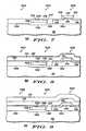
- FIGS. 7 - 11Attention is now directed to a method for forming exemplary portions of the integrated circuit 102 as illustrated in FIGS. 7 - 11 .
- a p-type doped, monocrystalline silicon substrate 110is provided having a compound semiconductor portion 1022 , a bipolar portion 1024 , and an MOS portion 1026 .
- the monocrystalline silicon substrateis doped to form an N + buried region 1102 .
- a lightly p-type doped epitaxial monocrystalline silicon layer 1104is then formed over the buried region 1102 and the substrate 110 .
- a doping stepis then performed to create a lightly n-type doped drift region 1117 above the N + buried region 1102 .
- the doping stepconverts the dopant type of the lightly p-type epitaxial layer within a section of the bipolar region 1024 to a lightly n-type monocrystalline silicon region.
- a field isolation region 1106is then formed between the bipolar portion 1024 and the MOS portion 1026 .
- a gate dielectric layer 1110is formed over a portion of the epitaxial layer 1104 within MOS portion 1026 , and the gate electrode 1112 is then formed over the gate dielectric layer 1110 .
- Sidewall spacers 1115are formed along vertical sides of the gate electrode 1112 and gate dielectric layer 1110 .
- a p-type dopantis introduced into the drift region 1117 to form an active or intrinsic base region 1114 .
- An n-type, deep collector region 1108is then formed within the bipolar portion 1024 to allow electrical connection to the buried region 1102 .
- Selective n-type dopingis performed to form N + doped regions 1116 and the emitter region 1120 .
- N + doped regions 1116are formed within layer 1104 along adjacent sides of the gate electrode 1112 and are source, drain, or source/drain regions for the MOS transistor.
- the N + doped regions 1116 and emitter region 1120have a doping concentration of at least 1E19 atoms per cubic centimeter to allow ohmic contacts to be formed.
- a p-type doped regionis formed to create the inactive or extrinsic base region 1118 which is a P + doped region (doping concentration of at least 1E19 atoms per cubic centimeter).
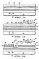
- An accommodating buffer layer 124is then formed over the substrate 110 as illustrated in FIG. 8.
- the accommodating buffer layerwill form as a monocrystalline layer over the properly prepared (i.e., having the appropriate template layer) bare silicon surface in portion 1022 .
- the portion of layer 124 that forms over portions 1024 and 1026may be polycrystalline or amorphous because it is formed over a material that is not monocrystalline, and therefore, does not nucleate monocrystalline growth.
- the accommodating buffer layer 124typically is a monocrystalline metal oxide or nitride layer and typically has a thickness in a range of approximately 2-100 nanometers. In one particular embodiment, the accommodating buffer layer is approximately 5-15 nm thick.
- an amorphous intermediate layer 122is formed along the uppermost silicon surfaces of the integrated circuit 102 .
- This amorphous intermediate layer 122typically includes an oxide of silicon and has a thickness and range of approximately 1-5 nm. In one particular embodiment, the thickness is approximately 2 nm.
- a template layer 126is then formed and has a thickness in a range of approximately one to ten monolayers of a material.
- the materialincludes titanium-arsenic, strontium-oxygen-arsenic, or other similar materials as previously described with respect to FIGS. 1 - 5 .
- a monocrystalline compound semiconductor layer 132is then epitaxially grown overlying the monocrystalline portion of accommodating buffer layer 124 as shown in FIG. 9.
- the portion of layer 132 that is grown over portions of layer 124 that are not monocrystallinemay be polycrystalline or amorphous.
- the monocrystalline compound semiconductor layercan be formed by a number of methods and typically includes a material such as gallium arsenide, aluminum gallium arsenide, indium phosphide, or other compounds semiconductor materials as previously mentioned.
- the thickness of the layeris in a range of approximately 1-5,000 nm, and more preferably 100-500 nm.
- each of the elements within the template layerare also present in the accommodating buffer layer 124 , the monocrystalline compound semiconductor material 132 , or both. Therefore, the delineation between the template layer 126 and its two immediately adjacent layers disappears during processing. Therefore, when a transmission electron microscopy (TEM) photograph is taken, an interface between the accommodating buffer layer 124 and the monocrystalline compound semiconductor layer 132 is seen.
- TEM
- the insulating layer 142can include a number of materials such as oxides, nitrides, oxynitrides, low-k dielectrics, or the like. As used herein, low-k is a material having a dielectric constant no higher than approximately 3.5. After the insulating layer 142 has been deposited, it is then polished, removing portions of the insulating layer 142 that overlie monocrystalline compound semiconductor layer 132 .
- a transistor 144is then formed within the monocrystalline compound semiconductor portion 1022 .
- a gate electrode 148is then formed on the monocrystalline compound semiconductor layer 132 .
- Doped regions 146are then formed within the monocrystalline compound semiconductor layer 132 .
- the transistor 144is a metal-semiconductor field-effect transistor (MESFET). If the MESFET is an n-type MESFET, the doped regions 146 and monocrystalline compound semiconductor layer 132 are also n-type doped. If a p-type MESFET were to be formed, then the doped regions 146 and monocrystalline compound semiconductor layer 132 would have just the opposite doping type.
- MESFETmetal-semiconductor field-effect transistor
- the heavier doped (N) regions 146allow ohmic contacts to be made to the monocrystalline compound semiconductor layer 132 .
- the active devices within the integrated circuithave been formed.
- This particular embodimentincludes an n-type MESFET, a vertical NPN bipolar transistor, and a planar n-channel MOS transistor.
- transistorsincluding P-channel MOS transistors, p-type vertical bipolar transistors, p-type MESFETs, and combinations of vertical and planar transistors, can be used.
- other electrical componentssuch as resistors, capacitors, diodes, and the like, may be formed in one or more of the portions 1022 , 1024 , and 1026 .
- An insulating layer 152is formed over the substrate 110 .
- the insulating layer 152may include an etch-stop or polish-stop region that is not illustrated in the FIG. 11.
- a second insulating layer 154is then formed over the first insulating layer 152 . Portions of layers 154 , 152 , 142 , 124 , and 122 are removed to define contact openings where the devices are to be interconnected. Interconnect trenches are formed within insulating layer 154 to provide the lateral connections between the contacts. As illustrated in FIG.
- interconnect 1562connects a source or drain region of the n-type MESFET within portion 1022 to the deep collector region 1108 of the NPN transistor within the bipolar portion 1024 .
- the emitter region 1120 of the NPN transistoris connected to one of the doped regions 1116 of the n-channel MOS transistor within the MOS portion 1026 .
- the other doped region 1116is electrically connected to other portions of the integrated circuit that are not shown.
- a passivation layer 156is formed over the interconnects 1562 , 1564 , and 1566 and insulating layer 154 .
- Other electrical connectionsare made to the transistors as illustrated as well as to other electrical or electronic components within the integrated circuit 102 but are not illustrated in the figures. Further, additional insulating layers and interconnects may be formed as necessary to form the proper interconnections between the various components within the integrated circuit 102 .
- active devices for both compound semiconductor and Group IV semiconductor materialscan be integrated into a single integrated circuit. Because there is some difficulty in incorporating both bipolar transistors and MOS transistors within a same integrated circuit, it may be possible to move some of the components within bipolar portion into the compound semiconductor portion 1022 or the MOS portion 1024 . More specifically, turning to the embodiment as described with respect to FIG. 6, the amplifiers 10248 and 10242 may be moved over to the compound semiconductor portion 1022 , and the converters 10244 and 10246 can be moved over into the MOS portion 1026 . Therefore, the requirement of special fabricating steps solely used for making a bipolar transistor can be eliminated. Therefore, there would only be a compound semiconductor portion and a MOS portion to the integrated circuit.
- an integrated circuitcan be formed such that it includes an optical laser in a compound semiconductor portion and an optical interconnect (waveguide) to an MOS transistor within a Group IV semiconductor region of the same integrated circuit.
- FIGS. 12 - 18include illustrations of one embodiment.
- FIG. 12includes an illustration of a cross-section view of a portion of an integrated circuit 160 that includes a monocrystalline silicon wafer 161 .
- An amorphous intermediate layer 162 and an accommodating buffer layer 164similar to those previously described, have been formed over wafer 161 .
- the layers needed to form the optical laserwill be formed first, followed by the layers needed for the MOS transistor.
- the lower mirror layer 166includes alternating layers of compound semiconductor materials.
- the first, third, and fifth films within the optical lasermay include a material such as gallium arsenide
- the second, fourth, and: sixth films within the lower mirror layer 166may include aluminum gallium arsenide or vice versa.
- Layer 168includes the active region that will be used for photon generation.
- Upper mirror layer 170is formed in a similar manner to the lower mirror layer 166 and includes alternating films of compound semiconductor materials.
- the upper mirror layer 170may be p-type doped compound semiconductor materials
- the lower mirror layer 166may be n-type doped compound semiconductor materials.
- Another accommodating buffer layer 172is formed over the upper mirror layer 170 .
- the accommodating buffer layers 164 and 172may include different materials. However, their function is essentially the same in that each is used for making a transition between a compound semiconductor layer and a monocrystalline Group IV semiconductor layer.
- a monocrystalline Group IV semiconductor layer 174is formed over the accommodating buffer layer 172 .
- the monocrystalline Grout IV semiconductor layer 174includes germanium, silicon germanium, silicon germanium carbide, or the like.
- the MOS portionis processed to form electrical components within this upper monocrystalline Group IV semiconductor layer 174 .
- a field isolation region 171is formed from a portion of layer 174 .
- a gate dielectric layer 173is formed over the layer 174 , and a gate electrode 175 is formed over the gate dielectric layer 173 .
- Doped regions 177are source, drain, or source/drain regions for the transistor 181 , as shown.
- Sidewall spacers 179are formed adjacent to the vertical sides of the gate electrode 175 .
- Other componentscan be made within at least a part of layer 174 . These other components include other transistors (n-channel or p-channel), capacitors, transistors, diodes, and the like.
- a monocrystalline Group IV semiconductor layeris epitaxially grown over one of the doped regions 177 .
- An upper portion 184is P+ doped, and a lower portion 182 remains substantially intrinsic (undoped) as illustrated in FIG. 13.
- the layercan be formed using a selective epitaxial process.
- an insulating layer(not shown) is formed over the transistor 181 and the field isolation region 171 .
- the insulating layeris patterned to define an opening that exposes one of the doped regions 177 .
- the selective epitaxial layeris formed without dopants.
- the entire selective epitaxial layermay be intrinsic, or a p-type dopant can be added near the end of the formation of the selective epitaxial layer. If the selective epitaxial layer is intrinsic, as formed, a doping step may be formed by implantation or by furnace doping. Regardless how the P+ upper portion 184 is formed, the insulating layer is then removed to form the resulting structure shown in FIG. 13.
- the next set of stepsis performed to define the optical laser 180 as illustrated in FIG. 14.
- the field isolation region 171 and the accommodating buffer layer 172are removed over the compound semiconductor portion of the integrated circuit. Additional steps are performed to define the upper mirror layer 170 and active layer 168 of the optical laser 180 .
- the sides of the upper mirror layer 170 and active layer 168are substantially coterminous.
- Contacts 186 and 188are formed for making electrical contact to the upper mirror layer 170 and the lower mirror layer 166 , respectively, as shown in FIG. 14.
- Contact 186has an annular shape to allow light (photons) to pass out of the upper mirror layer 170 into a subsequently formed optical waveguide.
- An insulating layer 190is then formed and patterned to define optical openings extending to the contact layer 186 and one of the doped regions 177 as shown in FIG. 15.
- the insulating materialcan be any number of different materials, including an oxide, nitride, oxynitride, low-k dielectric, or any combination thereof.
- a higher refractive index material 202is then formed within the openings to fill them and to deposit the layer over the insulating layer 190 as illustrated in FIG. 16.
- “higher”is in relation to the material of the insulating layer 190 (i.e., material 202 has a higher refractive index compared to the insulating layer 190 ).
- a relatively thin lower refractive index film(not shown) could be formed before forming the higher refractive index material 202 .
- a hard mask layer 204is then formed over the high refractive index layer 202 . Portions of the hard mask layer 204 , and high refractive index layer 202 are removed from portions overlying the opening and to areas closer to the sides of FIG. 16.
- a deposition procedure(possibly a dep-etch process) is performed to effectively create sidewalls sections 212 .
- the sidewall sections 212are made of the same material as material 202 .
- the hard mask layer 204is then removed, and a low refractive index layer 214 (low relative to material 202 and layer 212 ) is formed over the higher refractive index material 212 and 202 and exposed portions of the insulating layer 190 .
- the dash lines in FIG. 17illustrate the border between the high refractive index materials 202 and 212 . This designation is used to identify that both are made of the same material but are formed at different times.
- Processingis continued to form a substantially completed integrated circuit as illustrated in FIG. 18.
- a passivation layer 220is then formed over the optical laser 180 and MOSFET transistor 181 .
- other electrical or optical connectionsare made to the components within the integrated circuit but are not illustrated in FIG. 18.
- These interconnectscan include other optical waveguides or may include metallic interconnects.
- other types of laserscan be formed.
- another type of lasercan emit light (photons) horizontally instead of vertically. If light is emitted horizontally, the MOSFET transistor could be formed within the substrate 161 , and the optical waveguide would be reconfigured, so that the laser is properly coupled (optically connected) to the transistor.
- the optical waveguidecan include at least a portion of the accommodating buffer layer. Other configurations are possible.
- the compound semiconductor portionmay include light emitting diodes, photodetectors, diodes, or the like
- the Group IV semiconductorcan include digital logic, memory arrays, and most structures that can be formed in conventional MOS integrated circuits.
- a monocrystalline Group IV wafercan be used in forming only compound semiconductor electrical components over the wafer.
- the waferis essentially a “handle” wafer used during the fabrication of the compound semiconductor electrical components within a monocrystalline compound semiconductor layer overlying the wafer. Therefore, electrical components can be formed within III-V or II-VI semiconductor materials over a wafer of at least approximately 200 millimeters in diameter and possibly at least approximately 300 millimeters.
- a relatively inexpensive “handle” waferovercomes the fragile nature of the compound semiconductor wafers by placing them over a relatively more durable and easy to fabricate base material. Therefore, an integrated circuit can be formed such that all electrical components, and particularly all active electronic devices, can be formed within the compound semiconductor material even though the substrate itself may include a Group IV semiconductor material. Fabrication costs for compound semiconductor device should decrease because larger substrates can be processed more economically and more readily compared to the relatively smaller and more fragile, conventional compound semiconductor wafers.
Landscapes
- Engineering & Computer Science (AREA)
- Physics & Mathematics (AREA)
- Condensed Matter Physics & Semiconductors (AREA)
- General Physics & Mathematics (AREA)
- Manufacturing & Machinery (AREA)
- Computer Hardware Design (AREA)
- Microelectronics & Electronic Packaging (AREA)
- Power Engineering (AREA)
- Chemical & Material Sciences (AREA)
- Crystallography & Structural Chemistry (AREA)
- Materials Engineering (AREA)
- General Chemical & Material Sciences (AREA)
- Chemical Kinetics & Catalysis (AREA)
- Electromagnetism (AREA)
- Metallurgy (AREA)
- Organic Chemistry (AREA)
- Optics & Photonics (AREA)
- Recrystallisation Techniques (AREA)
- Semiconductor Memories (AREA)
- Metal-Oxide And Bipolar Metal-Oxide Semiconductor Integrated Circuits (AREA)
- Bipolar Integrated Circuits (AREA)
- Junction Field-Effect Transistors (AREA)
- Crystals, And After-Treatments Of Crystals (AREA)
- Semiconductor Lasers (AREA)
- Semiconductor Integrated Circuits (AREA)
- Bipolar Transistors (AREA)
- Formation Of Insulating Films (AREA)
- Solid State Image Pick-Up Elements (AREA)
Abstract
Description
- The present application is related to U.S. patent application Ser. No. 09/273,929 entitled “Method for Fabricating a Semiconductor Structure Having a Crystalline Alkaline Earth Metal Oxide Interface with Silicon,” filed 22 Mar. 1999, U.S. patent application Ser. No. 09/274,268 entitled “Semiconductor Structure Having a Crystalline Alkaline Earth Metal Oxide Interface with Silicon,” filed 22 Mar. 1999, and (Attorney Reference No. SC10903TP) entitled “Semiconductor Substrate and Method for Preparing the Same,” filed concurrently herewith, all of which are assigned to the current assignee hereof.[0001]
- This invention relates generally to semiconductor structures and devices and to a method for their fabrication, and more specifically to compound semiconductor structures and devices and to the fabrication and use of semiconductor structures, devices, and integrated circuits that include a monocrystalline compound semiconductor material.[0002]
- The vast majority of semiconductor discrete devices and integrated circuits are fabricated from silicon, at least in part because of the availability of inexpensive, high quality monocrystalline silicon substrates. Other semiconductor materials, such as the so called compound semiconductor materials, have physical attributes, including wider bandgap and/or higher mobility than silicon, or direct bandgaps that makes these materials advantageous for certain types of semiconductor devices. Unfortunately, compound semiconductor materials are generally much more expensive than silicon and are not available in large wafers as is silicon. Gallium arsenide (GaAs), the most readily available compound semiconductor material, is available in wafers only up to about 150 millimeters (mm) in diameter. In contrast, silicon wafers are available up to about 300 mm and are widely available at 200 mm. The 150 mm GaAs wafers are many times more expensive than are their silicon counterparts. Wafers of other compound semiconductor materials are even less available and are more expensive than GaAs.[0003]
- Because of the desirable characteristics of compound semiconductor materials, and because of their present generally high cost and low availability in bulk form, for many years attempts have been made to grow thin films of the compound semiconductor materials on a foreign substrate. To achieve optimal characteristics of the compound semiconductor material, however, a monocrystalline film of high crystalline quality is desired. Attempts have been made, for example, to grow layers of a monocrystalline compound semiconductor material on germanium, silicon, and various insulators. These attempts have generally been unsuccessful because lattice mismatches between the host crystal and the grown crystal have caused the resulting thin film of compound semiconductor material to be of low crystalline quality.[0004]
- If a large area thin film of high quality monocrystalline compound semiconductor material was available at low cost, a variety of semiconductor devices could advantageously be fabricated in that film at a low cost compared to the cost of fabricating such devices on a bulk wafer of compound semiconductor material or in an epitaxial film of such material on a bulk wafer of compound semiconductor material. In addition, if a thin film of high quality monocrystalline compound semiconductor material could be realized on a bulk wafer such as a silicon wafer, an integrated device structure could be achieved that took advantage of the best properties of both the silicon and the compound semiconductor material.[0005]
- Accordingly, a need exists for a semiconductor structure that provides a high quality monocrystalline compound semiconductor film over another monocrystalline material and for a process for making such a structure.[0006]
- The present invention is illustrated by way of example and not limitation in the accompanying figures, in which like references indicate similar elements, and in which:[0007]
- FIGS. 1, 2,[0008]4,5 illustrate schematically, in cross section, device structures in accordance with various embodiments of the invention;
- FIG. 3 illustrates graphically the relationship between maximum attainable film thickness and lattice mismatch between a host crystal and a grown crystalline overlayer;[0009]
- FIG. 6 includes an illustration of a block diagram of a portion of a communicating device;[0010]
- FIGS.[0011]7-11 include illustrations of cross-sectional views of a portion of an integrated circuit that includes a compound semiconductor portion, a bipolar portion, and an MOS portion; and
- FIGS.[0012]12-18 includes illustrations of cross-sectional views of a portion of another integrated circuit that includes a semiconductor laser and an MOS transistor.
- Skilled artisans will appreciate that elements in the figures are illustrated for simplicity and clarity and have not necessarily been drawn to scale. For example, the dimensions of some of the elements in the figures may be exaggerated relative to other elements to help to improve understanding of embodiments of the present invention.[0013]
- FIG. 1 illustrates schematically, in cross section, a portion of a[0014]
semiconductor structure 20 in accordance with an embodiment of the invention.Semiconductor structure 20 includes amonocrystalline substrate 22,accommodating buffer layer 24 comprising a monocrystalline material, and alayer 26 of a monocrystalline compound semiconductor material. In this context, the term “monocrystalline” shall have the meaning commonly used within the semiconductor industry. The term shall refer to materials that are a single crystal or that are substantially a single crystal and shall include those materials having a relatively small number of defects such as dislocations and the like as are commonly found in substrates of silicon or germanium or mixtures of silicon and germanium and epitaxial layers of such materials commonly found in the semiconductor industry. - In accordance with one embodiment of the invention,[0015]
structure 20 also includes an amorphousintermediate layer 28 positioned betweensubstrate 22 and accommodatingbuffer layer 24.Structure 20 may also include atemplate layer 30 between the accommodating buffer layer andcompound semiconductor layer 26. As will be explained more fully below, the template layer helps to initiate the growth of the compound semiconductor layer on the accommodating buffer layer. The amorphous intermediate layer helps to relieve the strain in the accommodating buffer layer and by doing so, aids in the growth of a high crystalline quality accommodating buffer layer. - [0016]
Substrate 22, in accordance with an embodiment of the invention, is a monocrystalline semiconductor wafer, preferably of large diameter. The wafer can be of a material from Group IV of the periodic table, and preferably a material from Group IVA. Examples of Group IV semiconductor materials include silicon, germanium, mixed silicon and germanium, mixed silicon and carbon, mixed silicon, germanium and carbon, and the like. Preferablysubstrate 22 is a wafer containing silicon or germanium, and most preferably is a high quality monocrystalline silicon wafer as used in the semiconductor industry. Accommodatingbuffer layer 24 is preferably a monocrystalline oxide or nitride material epitaxially grown on the underlying substrate. In accordance with one embodiment of the invention, amorphousintermediate layer 28 is grown onsubstrate 22 at the interface betweensubstrate 22 and the growing accommodating buffer layer by the oxidation ofsubstrate 22 during the growth oflayer 24. The amorphous intermediate layer serves to relieve strain that might otherwise occur in the monocrystalline accommodating buffer layer as a result of differences in the lattice constants of the substrate and the buffer layer. As used herein, lattice constants refers to the distance between atoms of a cell measured in the plane of the surface. If such strain is not relieved by the amorphous intermediate layer, the strain may cause defects in the crystalline structure of the accommodating buffer layer. Defects in the crystalline structure of the accommodating buffer layer, in turn, would make it difficult to achieve a high quality crystalline structure in monocrystallinecompound semiconductor layer 26. - Accommodating[0017]
buffer layer 24 is preferably a monocrystalline oxide or nitride material selected for its crystalline compatibility with the underlying substrate and with the overlying compound semiconductor material. For example, the material could be an oxide or nitride having a lattice structure matched to the substrate and to the subsequently applied semiconductor material. Materials that are suitable for the accommodating buffer layer include metal oxides such as the alkaline earth metal titanates, alkaline earth metal zirconates, alkaline earth metal hafnates, alkaline earth metal tantalates, alkaline earth metal ruthenates, alkaline earth metal niobates, alkaline earth metal vanadates, alkaline earth metal tin-based perovskites, lanthanum aluminate, lanthanum scandium oxide, and gadolinium oxide. Additionally, various nitrides such as gallium nitride, aluminum nitride, and boron nitride may also be used for the accommodating buffer layer. Most of these materials are insulators, although strontium ruthenate, for example, is a conductor. Generally, these materials are metal oxides or metal nitrides, and more particularly, these metal oxide or nitrides typically include at least two different metallic elements. In some specific applications, the metal oxides or nitride may include three or more different metallic elements. - [0018]
Amorphous interface layer 28 is preferably an oxide formed by the oxidation of the surface ofsubstrate 22, and more preferably is composed of a silicon oxide. The thickness oflayer 28 is sufficient to relieve strain attributed to mismatches between the lattice constants ofsubstrate 22 and accommodatingbuffer layer 24. Typically,layer 28 has a thickness in the range of approximately 0.5-5 nm. - The compound semiconductor material of[0019]
layer 26 can be selected, as needed for a particular semiconductor structure, from any of the Group IIIA and VA elements (III-V semiconductor compounds), mixed III-V compounds, Group II(A or B) and VIA elements (II-VI semiconductor compounds), and mixed II-VI compounds. Examples include gallium arsenide (GaAs), gallium indium arsenide (GaInAs), gallium aluminum arsenide (GaAlAs), indium phosphide (InP), cadmium sulfide (CdS), cadmium mercury telluride (CdHgTe), zinc selenide (ZnSe), zinc sulfur selenide (ZnSSe), and the like. Suitable template materials chemically bond to the surface of theaccommodating buffer layer 24 at selected sites and provide sites for the nucleation of the epitaxial growth of the subsequentcompound semiconductor layer 26. Appropriate materials fortemplate 30 are discussed below. - FIG. 2 illustrates, in cross section, a portion of a[0020]
semiconductor structure 40 in accordance with a further embodiment of the invention.Structure 40 is similar to the previously describedsemiconductor structure 20 except that anadditional buffer layer 32 is positioned betweenaccommodating buffer layer 24 and layer of monocrystallinecompound semiconductor material 26. Specifically, the additional buffer layer is positioned between thetemplate layer 30 and the overlying layer of compound semiconductor material. The additional buffer layer, formed of a semiconductor or compound semiconductor material, serves to provide a lattice compensation when the lattice constant of the accommodating buffer layer cannot be adequately matched to the overlying monocrystalline compound semiconductor material layer. - The following non-limiting, illustrative examples illustrate various combinations of materials useful in[0021]
structure 20 andstructure 40 in accordance with various alternative embodiments of the invention. These examples are merely illustrative, and it is not intended that the invention be limited to these illustrative examples. - In accordance with one embodiment of the invention,[0022]
monocrystalline substrate 22 is a silicon substrate oriented in the (100) direction. The silicon substrate can be, for example, a silicon substrate as is commonly used in making complementary metal oxide semiconductor (CMOS) integrated circuits having a diameter of about 200-300 mm. In accordance with this embodiment of the invention,accommodating buffer layer 24 is a monocrystalline layer of SrzBa1-zTiO3where z ranges from 0 to 1 and the amorphous intermediate layer is a layer of silicon oxide (SiOx) formed at the interface between the silicon substrate and the accommodating buffer layer. The value of z is selected to obtain one or more lattice constants closely matched to corresponding lattice constants of the subsequently formedlayer 26. The accommodating buffer layer can have a thickness of about 2 to about 100 nanometers (nm) and preferably has a thickness of about 10 nm. In general, it is desired to have an accommodating buffer layer thick enough to isolate the compound semiconductor layer from the substrate to obtain the desired electrical and optical properties. Layers thicker than 100 nm usually provide little additional benefit while increasing cost unnecessarily; however, thicker layers may be fabricated if needed. The amorphous intermediate layer of silicon oxide can have a thickness of about 0.5-5 nm, and preferably a thickness of about 1.5-2.5 nm. - In accordance with this embodiment of the invention, compound[0023]
semiconductor material layer 26 is a layer of gallium arsenide (GaAs) or aluminum gallium arsenide (AlGaAs) having a thickness of about 1 nm to about 100 micrometers (μm) and preferably a thickness of about 0.5 μm to 10 μm. The thickness generally depends on the application for which the layer is being prepared. To facilitate the epitaxial growth of the gallium arsenide or aluminum gallium arsenide on the monocrystalline oxide, a template layer is formed by capping the oxide layer. The template layer is preferably 1-10 monolayers of Ti—As, Sr—O—As, Sr—Ga—O, or Sr—Al—O. By way of a preferred example, 1-2 monolayers of Ti—As or Sr—Ga—O have been shown to successfully grow GaAs layers. - In accordance with a further embodiment of the invention,[0024]
monocrystalline substrate 22 is a silicon substrate as described above. The accommodating buffer layer is a monocrystalline oxide of strontium or barium zirconate or hafnate in a cubic or orthorhombic phase with an amorphous intermediate layer of silicon oxide formed at the interface between the silicon substrate and the accommodating buffer layer. The accommodating buffer layer can have a thickness of about 2-100 nm and preferably has a thickness of at least 5 nm to ensure adequate crystalline and surface quality and is formed of a monocrystalline SrZrO3, BaZrO3, SrHfO3, BaSnO3or BaHfO3. For example, a monocrystalline oxide layer of BaZrO3can grow at a temperature of about 700 degrees C. The lattice structure of the resulting crystalline oxide exhibits a 45 degree rotation with respect to the substrate silicon lattice structure. - An accommodating buffer layer formed of these zirconate or hafnate materials is suitable for the growth of compound semiconductor materials in the indium phosphide (InP) system. The compound semiconductor material can be, for example, indium phosphide (InP) or indium gallium arsenide (InGaAs) having a thickness of about 1.0 nm to 10 μm. A suitable template for this structure is 1-10 monolayers of zirconium-arsenic (Zr—As), zirconium-phosphorus (Zr—P), hafnium-arsenic (Hf—As), hafnium-phosphorus (Hf—P), strontium-oxygen-arsenic (Sr—O—As), strontium-oxygen-phosphorus (Sr—O—P), barium-oxygen-arsenic (Ba—O—As), indium-strontium-oxygen (In—Sr—O), or barium-oxygen-phosphorus (Ba—O—P), and preferably 1-2 monolayers of one of these materials. By way of an example, for a barium zirconate accommodating buffer layer, the surface is terminated with 1-2 monolayers of zirconium followed by deposition of 1-2 monolayers of arsenic to form a Zr—As template. A monocrystalline layer of the compound semiconductor material from the indium phosphide system is then grown on the template layer. The resulting lattice structure of the compound semiconductor material exhibits a 45 degree rotation with respect to the accommodating buffer layer lattice structure and a lattice mismatch to (100) InP of less than 2.5%, and preferably less than about 1.0%.[0025]
- In accordance with a further embodiment of the invention, a structure is provided that is suitable for the growth of an epitaxial film of a II-VI material overlying a silicon substrate. The substrate is preferably a silicon wafer as described above. A suitable accommodating buffer layer material is Sr[0026]xBa1-xTiO3, where x ranges from 0 to 1, having a thickness of about 2-100 nm and preferably a thickness of about 5-15 nm. The II-VI compound semiconductor material can be, for example, zinc selenide (ZnSe) or zinc sulfur selenide (ZnSSe). A suitable template for this material system includes 1-10 monolayers of zinc-oxygen (Zn—O) followed by 1-2 monolayers of an excess of zinc followed by the selenidation of zinc on the surface. Alternatively, a template can be, for example, strontium-sulfur (Sr—S) followed by the ZnSeS.
- This embodiment of the invention is an example of[0027]
structure 40 illustrated in FIG. 2.Substrate 22,monocrystalline oxide layer 24, and monocrystalline compoundsemiconductor material layer 26 can be similar to those described in example 1. In addition, anadditional buffer layer 32 serves to alleviate any strains that might result from a mismatch of the crystal lattice of the accommodating buffer layer and the lattice of the monocrystalline semiconductor material.Buffer layer 32 can be a gallium arsenide phosphide (GaAsxP1-x) or indium gallium phosphide (InyGa1-yP) strain compensated superlattice. In the gallium arsenide phosphide superlattice the value of x ranges from 0 to 1, and in the indium gallium phosphide superlattice the value of y ranges from 0 to 1. By so varying the value of x or y, as the case may be, the lattice constant is varied from bottom to top across the superlattice to create a match between lattice constants of the underlying oxide and the overlying compound semiconductor material. The superlattice can have a thickness of about 50-500 nm and preferably has a thickness of about 200-100 nm. The template for this structure can be the same of that described in example 1. Alternatively, the buffer layer can be a layer of monocrystalline germanium having a thickness of 1-50 nm and preferably having a thickness of about 2-20 nm. In using a germanium buffer layer, a template layer of either germanium-strontium (Ge—Sr) or germanium-titanium (Ge—Ti) having a thickness of about one monolayer can be used. The formation of the oxide layer is capped with either a monolayer of strontium or a monolayer of titanium to act as a nucleating site for the subsequent deposition of the monocrystalline germanium. The monolayer of strontium or titanium provides a nucleating site to which the first monolayer of germanium can bond. - This example also illustrates materials useful in a[0028]
structure 40 as illustrated in FIG. 2.Substrate material 22,accommodating buffer layer 24, monocrystalline compoundsemiconductor material layer 26 andtemplate layer 30 can be the same as those described above in example 2. In addition, abuffer layer 32 is inserted between the accommodating buffer layer and the overlying monocrystalline compound semiconductor material layer. The buffer layer, a further monocrystalline semiconductor material, can be, for example, a graded layer of indium gallium arsenide (InGaAs) in which the indium composition varies from 0 to about 47%. The buffer layer preferably has a thickness of about 10-30 nm. Varying the composition of the buffer layer from GaAs to InGaAs serves to provide a lattice match between the underlying monocrystalline oxide material and the overlying layer of monocrystalline compound semiconductor material. Such a buffer layer is especially advantageous if there is a lattice mismatch betweenaccommodating buffer layer 24 and monocrystalline compoundsemiconductor material layer 26. - Referring again to FIGS. 1 and 2,[0029]
substrate 22 is a monocrystalline substrate such as a monocrystalline silicon substrate. The crystalline structure of the monocrystalline substrate is characterized by a lattice constant and by a lattice orientation. In similar manner,accommodating buffer layer 24 is also a monocrystalline material and the lattice of that monocrystalline material is characterized by a lattice constant and a crystal orientation. The lattice constants of the accommodating buffer layer and the monocrystalline substrate must be closely matched or, alternatively, must be such that upon rotation of one crystal orientation with respect to the other crystal orientation, a substantial match in lattice constants is achieved. In this context the terms “substantially equal” and “substantially matched” mean that there is sufficient similarity between the lattice constants to permit the growth of a high quality crystalline layer on the underlying layer. - FIG. 3 illustrates graphically the relationship of the achievable thickness of a grown crystal layer of high crystalline quality as a function of the mismatch between the lattice constants of the host crystal and the grown crystal.[0030]
Curve 42 illustrates the boundary of high crystalline quality material. The area to the right ofcurve 42 represents layers that tend to be polycrystalline. With no lattice mismatch, it is theoretically possible to grow an infinitely thick, high quality epitaxial layer on the host crystal. As the mismatch in lattice constants increases, the thickness of achievable, high quality crystalline layer decreases rapidly. As a reference point, for example, if the lattice constants between the host crystal and the grown layer are mismatched by more than about 2%, monocrystalline epitaxial layers in excess of about 20 nm cannot be achieved. - In accordance with one embodiment of the invention,[0031]
substrate 22 is a (100) or (111) oriented monocrystalline silicon wafer andaccommodating buffer layer 24 is a layer of strontium barium titanate. Substantial matching of lattice constants between these two materials is achieved by rotating the crystal orientation of the titanate material by 45° with respect to the crystal orientation of the silicon substrate wafer. The inclusion in the structure ofamorphous interface layer 24, a silicon oxide layer in this example, serves to reduce strain in the titanate monocrystalline layer that might result from any mismatch in the lattice constants of the host silicon wafer and the grown titanate layer. As a result, in accordance with an embodiment of the invention, a high quality, thick monocrystalline titanate layer is achievable. - Still referring to FIGS. 1 and 2,[0032]
layer 26 is a layer of epitaxially grown monocrystalline compound semiconductor material and that crystalline material is also characterized by a crystal lattice constant and a crystal orientation. To achieve high crystalline quality in this epitaxially grown layer, the accommodating buffer layer must be of high crystalline quality. In addition, in order to achieve high crystalline quality inlayer 26, substantial matching between the crystal lattice constant of the host crystal, in this case, the monocrystalline accommodating buffer layer, and the grown crystal is desired. With properly selected materials this substantial matching of lattice constants is achieved as a result of rotation of the crystal orientation of the grown crystal with respect to the orientation of the host crystal. If the grown crystal is gallium arsenide, aluminum gallium arsenide, zinc selenide, or zinc sulfur selenide and the accommodating buffer layer is monocrystalline SrxBa1-xTiO3, substantial matching of crystal lattice constants of the two materials is achieved, wherein the crystal orientation of the grown layer is rotated by 45° with respect to the orientation of the host monocrystalline oxide. Similarly, if the host material is a strontium or barium zirconate or a strontium or barium hafnate or barium tin oxide and the compound semiconductor layer is indium phosphide or gallium indium arsenide or aluminum indium arsenide, substantial matching of crystal lattice constants can be achieved by rotating the orientation of the grown crystal layer by 45° with respect to the host oxide crystal. In some instances, a crystalline semiconductor buffer layer between the host oxide and the grown compound semiconductor layer can be used to reduce strain in the grown monocrystalline compound semiconductor layer that might result from small differences in lattice constants. Better crystalline quality in the grown monocrystalline compound semiconductor layer can thereby be achieved. - The following example illustrates a process, in accordance with one embodiment of the invention, for fabricating a semiconductor structure such as the structures depicted in FIGS. 1 and 2. The process starts by providing a monocrystalline semiconductor substrate comprising silicon or germanium. In accordance with a preferred embodiment of the invention, the semiconductor substrate is a silicon wafer having a (100) orientation. The substrate is preferably oriented on axis or, at most, about 0.5° off axis. At least a portion of the semiconductor substrate has a bare surface, although other portions of the substrate, as described below, may encompass other structures. The term “bare” in this context means that the surface in the portion of the substrate has been cleaned to remove any oxides, contaminants, or other foreign material. As is well known, bare silicon is highly reactive and readily forms a native oxide. The term “bare” is intended to encompass such a native oxide. A thin silicon oxide may also be intentionally grown on the semiconductor substrate, although such a grown oxide is not essential to the process in accordance with the invention. In order to epitaxially grow a monocrystalline oxide layer overlying the monocrystalline substrate, the native oxide layer must first be removed to expose the crystalline structure of the underlying substrate. The following process is preferably carried out by molecular beam epitaxy (MBE). The native oxide can be removed by first thermally depositing a thin layer of strontium in an MBE apparatus. The substrate is then heated to a temperature of about 750° C. to cause the strontium to react with the native silicon oxide layer. The strontium serves to reduce the silicon oxide to leave a silicon oxide-free surface. The resultant surface, which exhibits an ordered 2×1 structure, includes strontium, oxygen, and silicon. The ordered 2×1 structure forms a template for the ordered growth of an overlying layer of a monocrystalline oxide. The template provides the necessary chemical and physical properties to nucleate the crystalline growth of an overlying layer.[0033]
- In accordance with an alternate embodiment of the invention, the native silicon oxide can be converted and the substrate surface can be prepared for the growth of a monocrystalline oxide layer by depositing strontium oxide onto the substrate surface by MBE at a low temperature and by subsequently heating the structure to a temperature of about 750° C. At this temperature a solid state reaction takes place between the strontium oxide and the native silicon oxide causing the reduction of the native silicon oxide and leaving an ordered 2×1 structure with strontium, oxygen, and silicon remaining on the substrate surface. Again, this forms a template for the subsequent growth of an ordered monocrystalline oxide layer.[0034]
- Following the removal of the silicon oxide from the surface of the substrate, in accordance with one embodiment of the invention, the substrate is cooled to a temperature in the range of about 400-600° C. and a layer of strontium titanate is grown on the template layer by molecular beam epitaxy. The MBE process is initiated by opening shutters in the MBE apparatus to expose strontium, titanium and oxygen sources. The ratio of strontium and titanium is approximately 1:1. The partial pressure of oxygen is initially set at a minimum value to grow stochiometric strontium titanate at a growth rate of about 0.3-0.5 nm per minute. After initiating growth of the strontium titanate, the partial pressure of oxygen is increased above the initial minimum value. The overpressure of oxygen causes the growth of an amorphous silicon oxide layer at the interface between the underlying substrate and the growing strontium titanate layer. The growth of the silicon oxide layer results from the diffusion of oxygen through the growing strontium titanate layer to the interface where the oxygen reacts with silicon at the surface of the underlying substrate. The strontium titanate grows as an ordered monocrystal with the crystalline orientation rotated by 45° with respect to the ordered 2×1 crystalline structure of the underlying substrate. Strain that otherwise might exist in the strontium titanate layer because of the small mismatch in lattice constant between the silicon substrate and the growing crystal is relieved in the amorphous silicon oxide intermediate layer.[0035]
- After the strontium titanate layer has been grown to the desired thickness, the monocrystalline strontium titanate is capped by a template layer that is conducive to the subsequent growth of an epitaxial layer of a desired compound semiconductor material. For the subsequent growth of a layer of gallium arsenide, the MBE growth of the strontium titanate monocrystalline layer can be capped by terminating the growth with 1-2 monolayers of titanium, 1-2 monolayers of titanium-oxygen or with 1-2 monolayers of strontium-oxygen. Following the formation of this capping layer, arsenic is deposited to form a Ti—As bond, a Ti—O—As bond or a Sr—O—As. Any of these form an appropriate template for deposition and formation of a gallium arsenide monocrystalline layer. Following the formation of the template, gallium is introduced to the reaction with the arsenic and gallium arsenide forms. Alternatively, gallium can be deposited on the capping layer to form a Sr—O—Ga bond, and arsenic is introduced with the gallium to form the GaAs.[0036]
- The structure illustrated in FIG. 2 can be formed by the process discussed above with the addition of an additional buffer layer deposition step. The buffer layer is formed overlying the template layer before the deposition of the monocrystalline compound semiconductor layer. If the buffer layer is a compound semiconductor superlattice, such a superlattice can be deposited, by MBE for example, on the template described above. If instead the buffer layer is a layer of germanium, the process above is modified to cap the strontium titanate monocrystalline layer with a final layer of either strontium or titanium and then by depositing germanium to react with the strontium or titanium. The germanium buffer layer can then be deposited directly on this template.[0037]
- The process described above illustrates a process for forming a semiconductor structure including a silicon substrate, a monocrystalline strontium titanate accommodating buffer layer, and a monocrystalline gallium arsenide compound semiconductor layer by the process of molecular beam epitaxy. The process can also be carried out by the process of chemical vapor deposition (CVD), metal organic chemical vapor deposition (MOCVD), migration enhanced epitaxy (MEE), atomic layer epitaxy (ALE), or the like. Further, by a similar process, other monocrystalline accommodating buffer layers such as alkaline earth metal titanates, zirconates, hafnates, tantalates, vanadates, ruthenates, and niobates, alkaline earth metal tin-based perovskites, lanthanum aluminate, lanthanum scandium oxide, and gadolinium oxide can also be grown. Further, by a similar process such as MBE, other III-V and II-VI monocrystalline compound semiconductor layers can be deposited overlying the monocrystalline oxide accommodating buffer layer.[0038]
- Each of the variations of compound semiconductor materials and monocrystalline oxide accommodating buffer layer uses an appropriate template for initiating the grown of the compound semiconductor layer. For example, if the accommodating buffer layer is alkaline earth metal zirconate, the oxide can be capped by a thin layer of zirconium. The deposition of zirconium can be followed by the deposition of arsenic or phosphorus to react with the zirconium as a precursor to depositing indium gallium arsenide, indium aluminum arsenide, or indium phosphide respectively. Similarly, if the monocrystalline oxide accommodating buffer layer is an alkaline earth metal hafnate, the oxide layer can be capped by a thin layer of hafnium. The deposition of hafnium is followed by the deposition of arsenic or phosphorous to react with the hafnium as a precursor to the growth of an indium gallium arsenide, indium aluminum arsenide, or indium phosphide layer, respectively. In a similar manner, strontium titanate can be capped with a layer of strontium or strontium and oxygen and barium titanate can be capped with a layer of barium or barium and oxygen. Each of these depositions can be followed by the deposition of arsenic or phosphorus to react with the capping material to form a template for the deposition of a compound semiconductor material layer comprising indium gallium arsenide, indium aluminum arsenide, or indium phosphide.[0039]
- FIG. 4 illustrates schematically, in cross section, a[0040]
device structure 50 in accordance with a further embodiment of the invention.Device structure 50 includes amonocrystalline semiconductor substrate 52, preferably a monocrystalline silicon wafer.Monocrystalline semiconductor substrate 52 includes two regions,53 and54. An electrical semiconductor component generally indicated by the dashedline 56 is formed inregion 53.Electrical component 56 can be a resistor, a capacitor, an active semiconductor component such as a diode or a transistor or an integrated circuit such as a CMOS integrated circuit. For example,electrical semiconductor component 56 can be a CMOS integrated circuit configured to perform digital signal processing or another function for which silicon integrated circuits are well suited. The electrical semiconductor component inregion 53 can be formed by conventional semiconductor processing as well known and widely practiced in the semiconductor industry. A layer of insulatingmaterial 58 such as a layer of silicon dioxide or the like may overlieelectrical semiconductor component 56. - Insulating[0041]
material 58 and any other layers that may have been formed or deposited during the processing ofsemiconductor component 56 inregion 53 are removed from the surface ofregion 54 to provide a bare silicon surface in that region. As is well known, bare silicon surfaces are highly reactive and a native silicon oxide layer can quickly form on the bare surface. A layer of barium or barium and oxygen is deposited onto the native oxide layer on the surface ofregion 54 and is reacted with the oxidized surface to form a first template layer (not shown). In accordance with one embodiment of the invention amonocrystalline oxide layer 60 is formed overlying the template layer by a process of molecular beam epitaxy. Reactants including barium, titanium and oxygen are deposited onto the template layer to form the monocrystalline oxide layer. Initially during the deposition the partial pressure of oxygen is kept near the minimum necessary to fully react with the barium and titanium to form monocrystallinebarium titanate layer 60. The partial pressure of oxygen is then increased to provide an overpressure of oxygen and to allow oxygen to diffuse through the growing monocrystalline oxide layer. The oxygen diffusing through the barium titanate reacts with silicon at the surface ofregion 54 to form anamorphous layer 62 of silicon oxide on the second region and at the interface between the silicon substrate and the monocrystalline oxide. - In accordance with an embodiment of the invention, the step of depositing[0042]
monocrystalline oxide layer 60 is terminated by depositing asecond template layer 64, which can be 1-10 monolayers of titanium., barium, barium and oxygen, or titanium and oxygen. Alayer 66 of a monocrystalline compound semiconductor material is then deposited overlying the second template layer by a process of molecular beam epitaxy. The deposition oflayer 66 is initiated by depositing a layer of arsenic onto the template. This initial step is followed by depositing gallium and arsenic to form monocrystalline gallium arsenide. Alternatively, strontium can be substituted for barium in the above example. - In accordance with a further embodiment of the invention, a semiconductor component, generally indicated by a dashed[0043]
line 68 is formed incompound semiconductor layer 66.Semiconductor component 68 can be formed by processing steps conventionally used in the fabrication of gallium arsenide or other III-V compound semiconductor material devices.Semiconductor component 68 can be any active or passive component, and preferably is a semiconductor laser, light emitting diode, photodetector, heterojunction bipolar transistor (HBT), high frequency MESFET, or other component that utilizes and takes advantage of the physical properties of compound semiconductor materials. A metallic conductor schematically indicated by theline 70 can be formed toelectrically couple device 68 anddevice 56, thus implementing an integrated device that includes at least one component formed in the silicon substrate and one device formed in the monocrystalline compound semiconductor material layer. Althoughillustrative structure 50 has been described as a structure formed on asilicon substrate 52 and having a barium (or strontium)titanate layer 60 and agallium arsenide layer 66, similar devices can be fabricated using other substrates, monocrystalline oxide layers and other compound semiconductor layers as described elsewhere in this disclosure. - FIG. 5 illustrates a semiconductor structure[0044]72 in accordance with a further embodiment of the invention. Structure72 includes a
monocrystalline semiconductor substrate 74 such as a monocrystalline silicon wafer that includes aregion 75 and aregion 76. An electrical component schematically illustrated by the dashedline 78 is formed inregion 75 using conventional silicon device processing techniques commonly used in the semiconductor industry. Using process steps similar to those described above, amonocrystalline oxide layer 80 and an intermediate amorphoussilicon oxide layer 82 are formedoverlying region 76 ofsubstrate 74. Atemplate layer 84 and subsequently amonocrystalline semiconductor layer 86 are formed overlyingmonocrystalline oxide layer 80. In accordance with a further embodiment of the invention, an additionalmonocrystalline oxide layer 88 is formedoverlying layer 86 by process steps similar to those used to formlayer 80, and an additionalmonocrystalline semiconductor layer 90 is formed overlyingmonocrystalline oxide layer 88 by process steps similar to those used to formlayer 86. In accordance with one embodiment of the invention, at least one oflayers - A semiconductor component generally indicated by a dashed[0045]
line 92 is formed at least partially inmonocrystalline semiconductor layer 86. In accordance with one embodiment of the invention,semiconductor component 92 may include a field effect transistor having a gate dielectric formed, in part, bymonocrystalline oxide layer 88. In addition,monocrystalline semiconductor layer 92 can be used to implement the gate electrode of that field effect transistor. In accordance with one embodiment of the invention,monocrystalline semiconductor layer 86 is formed from a group III-V compound andsemiconductor component 92 is a radio frequency amplifier that takes advantage of the high mobility characteristic of group III-V component materials. In accordance with yet a further embodiment of the invention, an electrical interconnection schematically illustrated by theline 94electrically interconnects component 78 andcomponent 92. Structure72 thus integrates components that take advantage of the unique properties of the two monocrystalline semiconductor materials. - By way of more specific examples, other integrated circuits and systems are illustrated in FIGS.[0046]6-18. FIG. 6 includes a simplified block diagram illustrating a portion of a communicating
device 100 having a signal transceiving means101., anintegrated circuit 102, anoutput unit 103, and aninput unit 104. Examples of the signal transceiving means include an antenna, a modem, or any other means by which information or data can be sent either to or from an external unit. As used herein, transceiving is used to denote that the signal transceiving means may be capable of only receiving, only transmitting, or both receiving and transmitting signals from or to the communicating device. Theoutput unit 103 can include a display, a monitor, a speaker, or the like. The input unit can include a microphone, a keyboard, or the like. Note that in alternative embodiments theoutput unit 103 andinput unit 104 could be replaced by a single unit such as a memory, or the like. The memory can include random access memory or nonvolatile memory, such as a hard disk, a flash memory card or module, or the like. - An integrated circuit is generally a combination of at least two circuit elements (e.g., transistors, diodes, resistors, capacitors, and the like) inseparably associated on or within a continuous substrate. The[0047]
integrated circuit 102 includes acompound semiconductor portion 1022, abipolar portion 1024, and anMOS portion 1026. Thecompound semiconductor portion 1022 includes electrical components that are formed at least partially within a compound semiconductor material. Transistors and other electrical components within thecompound semiconductor portion 1022 are capable of processing signals at radio frequencies of at least approximately 0.8 GHz. In other embodiments, the signals could be at lower or higher frequencies. For example, some materials, such as indium gallium arsenide, are capable of processing signals at radio frequency signals at approximately 27 GHz. - The[0048]
compound semiconductor portion 1022 further includes aduplexer 10222, a radio frequency-to-baseband converter10224 (demodulating means or demodulating circuit), baseband-to-radio frequency converter10226 (modulating means or modulating circuit), apower amplifier 10228, and anisolator 10229. Thebipolar portion 1024 and theMOS portion 1026 typically are formed in a Group IV semiconductive material. Thebipolar portion 1024 includes a receivingamplifier 10242, an analog-to-digital converter 10244, a digital-to-analog converter 10246, and a transmittingamplifier 10248. TheMOS portion 1026 includes a digital signal processing means10262. An example of such means includes any one of the commonly available DSP cores available in the market, such as the Motorola DSP 566xx (from Motorola, Incorporated of Schaumburg, Ill.) and Texas Instruments TMS 320C54x (from Texas Instruments of Dallas, Tex.) families of digital signal processors. This digital signal processing means10262 typically includes complementary MOS (CMOS) transistors and analog-to-digital and digital-to-analog converters. Clearly, other electrical components are present in the integrated circuit,102. - In one mode of operation, the communicating[0049]
device 100 receives a signal from an antenna, which is part of the signal transceiving means101. The signal passes through the duplexer10227 to the radio frequency-to-baseband converter 10224. The analog data or other information is amplified by receivingamplifier 10224 and transmitted to the digital signal processing means10262. After the digital signal processing means10262 has processed the information or other data, the processed information or other data is transmitted to theoutput unit 103. If the communicating device is a pager, the output unit can be a display. If the communicating device is a cellular telephone, theoutput unit 103 can include a speaker, a display, or both. - Data or other information can be sent through the communicating[0050]
device 100 in the opposite direction. The data or other information will come in through theinput unit 104. In a cellular telephone, this could include a microphone or a keypad. The information or other data is then processed using the digital signal processing means10262. After processing, the signal is then converted using the digital-to-analog converter 10246. The converted signal is amplified by the transmittingamplifier 10248. The amplified signal is modulated by the baseband-to-radio frequency converter 10226 and further amplified bypower amplifier 10228. The amplified RF signal passes through theisolator 10229 andduplexer 10222 to the antenna. - Prior art embodiments of the communicating[0051]
device 100 would have at least two separate integrated circuits: one for thecompound semiconductor portion 1022 and one for theMOS portion 1026. Thebipolar portion 1024 may be on the same integrated circuit as theMOS portion 1026 or could be on still another integrated circuit. With an embodiment of the present invention, all three portions can now be formed within a single integrated circuit. Because all of the transistors can reside on a single integrated circuit, the communicating device can be greatly miniaturized and allow for greater portability of a communicating device. - Attention is now directed to a method for forming exemplary portions of the[0052]
integrated circuit 102 as illustrated in FIGS.7-11. In FIG. 7, a p-type doped,monocrystalline silicon substrate 110 is provided having acompound semiconductor portion 1022, abipolar portion 1024, and anMOS portion 1026. Within the bipolar portion, the monocrystalline silicon substrate is doped to form an N+ buriedregion 1102. A lightly p-type doped epitaxialmonocrystalline silicon layer 1104 is then formed over the buriedregion 1102 and thesubstrate 110. A doping step is then performed to create a lightly n-type dopeddrift region 1117 above the N+ buriedregion 1102. The doping step converts the dopant type of the lightly p-type epitaxial layer within a section of thebipolar region 1024 to a lightly n-type monocrystalline silicon region. Afield isolation region 1106 is then formed between thebipolar portion 1024 and theMOS portion 1026. Agate dielectric layer 1110 is formed over a portion of theepitaxial layer 1104 withinMOS portion 1026, and thegate electrode 1112 is then formed over thegate dielectric layer 1110.Sidewall spacers 1115 are formed along vertical sides of thegate electrode 1112 andgate dielectric layer 1110. - A p-type dopant is introduced into the[0053]
drift region 1117 to form an active orintrinsic base region 1114. An n-type,deep collector region 1108 is then formed within thebipolar portion 1024 to allow electrical connection to the buriedregion 1102. Selective n-type doping is performed to form N+ dopedregions 1116 and theemitter region 1120. N+ dopedregions 1116 are formed withinlayer 1104 along adjacent sides of thegate electrode 1112 and are source, drain, or source/drain regions for the MOS transistor. The N+ dopedregions 1116 andemitter region 1120 have a doping concentration of at least 1E19 atoms per cubic centimeter to allow ohmic contacts to be formed. A p-type doped region is formed to create the inactive orextrinsic base region 1118 which is a P+ doped region (doping concentration of at least 1E19 atoms per cubic centimeter). - In the embodiment described, several processing steps have been performed but are not illustrated or further described, such as the formation of well regions, threshold adjusting implants, channel punchthrough prevention implants, field punchthrough prevention implants, as well as a variety of masking layers. The formation of the device up to this point in the process is performed using conventional steps. As illustrated, a standard N-channel MOS transistor has been formed within the[0054]
MOS region 1026, and a vertical NPN bipolar transistor has been formed within thebipolar portion 1024. As of this point, no circuitry has been formed within thecompound semiconductor portion 1022. - All of the layers that have been formed during the processing of the bipolar and MOS portions of the integrated circuit are now removed from the surface of[0055]
compound semiconductor portion 1022. A bare silicon surface is thus provided for the subsequent processing of this portion, for example in the manner set forth above. - An[0056]
accommodating buffer layer 124 is then formed over thesubstrate 110 as illustrated in FIG. 8. The accommodating buffer layer will form as a monocrystalline layer over the properly prepared (i.e., having the appropriate template layer) bare silicon surface inportion 1022. The portion oflayer 124 that forms overportions accommodating buffer layer 124 typically is a monocrystalline metal oxide or nitride layer and typically has a thickness in a range of approximately 2-100 nanometers. In one particular embodiment, the accommodating buffer layer is approximately 5-15 nm thick. During the formation of the accommodating buffer layer, an amorphousintermediate layer 122 is formed along the uppermost silicon surfaces of theintegrated circuit 102. This amorphousintermediate layer 122 typically includes an oxide of silicon and has a thickness and range of approximately 1-5 nm. In one particular embodiment, the thickness is approximately 2 nm. Following the formation of theaccommodating buffer layer 124 and the amorphousintermediate layer 122, atemplate layer 126 is then formed and has a thickness in a range of approximately one to ten monolayers of a material. In one particular embodiment, the material includes titanium-arsenic, strontium-oxygen-arsenic, or other similar materials as previously described with respect to FIGS.1-5. - A monocrystalline[0057]
compound semiconductor layer 132 is then epitaxially grown overlying the monocrystalline portion ofaccommodating buffer layer 124 as shown in FIG. 9. The portion oflayer 132 that is grown over portions oflayer 124 that are not monocrystalline may be polycrystalline or amorphous. The monocrystalline compound semiconductor layer can be formed by a number of methods and typically includes a material such as gallium arsenide, aluminum gallium arsenide, indium phosphide, or other compounds semiconductor materials as previously mentioned. The thickness of the layer is in a range of approximately 1-5,000 nm, and more preferably 100-500 nm. In this particular embodiment, each of the elements within the template layer are also present in theaccommodating buffer layer 124, the monocrystallinecompound semiconductor material 132, or both. Therefore, the delineation between thetemplate layer 126 and its two immediately adjacent layers disappears during processing. Therefore, when a transmission electron microscopy (TEM) photograph is taken, an interface between theaccommodating buffer layer 124 and the monocrystallinecompound semiconductor layer 132 is seen. - At this point in time, sections of the[0058]
compound semiconductor layer 132 and theaccommodating buffer layer 124 are removed from portions overlying thebipolar portion 1024 and theMOS portion 1026 as shown in FIG. 10. After the section is removed, an insulatinglayer 142 is then formed over thesubstrate 110. The insulatinglayer 142 can include a number of materials such as oxides, nitrides, oxynitrides, low-k dielectrics, or the like. As used herein, low-k is a material having a dielectric constant no higher than approximately 3.5. After the insulatinglayer 142 has been deposited, it is then polished, removing portions of the insulatinglayer 142 that overlie monocrystallinecompound semiconductor layer 132. - A[0059]
transistor 144 is then formed within the monocrystallinecompound semiconductor portion 1022. Agate electrode 148 is then formed on the monocrystallinecompound semiconductor layer 132.Doped regions 146 are then formed within the monocrystallinecompound semiconductor layer 132. In this embodiment, thetransistor 144 is a metal-semiconductor field-effect transistor (MESFET). If the MESFET is an n-type MESFET, the dopedregions 146 and monocrystallinecompound semiconductor layer 132 are also n-type doped. If a p-type MESFET were to be formed, then thedoped regions 146 and monocrystallinecompound semiconductor layer 132 would have just the opposite doping type. The heavier doped (N)regions 146 allow ohmic contacts to be made to the monocrystallinecompound semiconductor layer 132. At this point in time, the active devices within the integrated circuit have been formed. This particular embodiment includes an n-type MESFET, a vertical NPN bipolar transistor, and a planar n-channel MOS transistor. Many other types of transistors, including P-channel MOS transistors, p-type vertical bipolar transistors, p-type MESFETs, and combinations of vertical and planar transistors, can be used. Also, other electrical components, such as resistors, capacitors, diodes, and the like, may be formed in one or more of theportions - Processing continues to form a substantially completed[0060]
integrated circuit 102 as illustrated in FIG. 11. An insulatinglayer 152 is formed over thesubstrate 110. The insulatinglayer 152 may include an etch-stop or polish-stop region that is not illustrated in the FIG. 11. A second insulatinglayer 154 is then formed over the first insulatinglayer 152. Portions oflayers layer 154 to provide the lateral connections between the contacts. As illustrated in FIG. 11,interconnect 1562 connects a source or drain region of the n-type MESFET withinportion 1022 to thedeep collector region 1108 of the NPN transistor within thebipolar portion 1024. Theemitter region 1120 of the NPN transistor is connected to one of the dopedregions 1116 of the n-channel MOS transistor within theMOS portion 1026. The otherdoped region 1116 is electrically connected to other portions of the integrated circuit that are not shown. - A[0061]
passivation layer 156 is formed over theinterconnects layer 154. Other electrical connections are made to the transistors as illustrated as well as to other electrical or electronic components within theintegrated circuit 102 but are not illustrated in the figures. Further, additional insulating layers and interconnects may be formed as necessary to form the proper interconnections between the various components within theintegrated circuit 102. - As can be seen from the previous embodiment, active devices for both compound semiconductor and Group IV semiconductor materials can be integrated into a single integrated circuit. Because there is some difficulty in incorporating both bipolar transistors and MOS transistors within a same integrated circuit, it may be possible to move some of the components within bipolar portion into the[0062]
compound semiconductor portion 1022 or theMOS portion 1024. More specifically, turning to the embodiment as described with respect to FIG. 6, theamplifiers compound semiconductor portion 1022, and theconverters MOS portion 1026. Therefore, the requirement of special fabricating steps solely used for making a bipolar transistor can be eliminated. Therefore, there would only be a compound semiconductor portion and a MOS portion to the integrated circuit. - In still another embodiment, an integrated circuit can be formed such that it includes an optical laser in a compound semiconductor portion and an optical interconnect (waveguide) to an MOS transistor within a Group IV semiconductor region of the same integrated circuit. FIGS.[0063]12-18 include illustrations of one embodiment.
- FIG. 12 includes an illustration of a cross-section view of a portion of an integrated circuit[0064]160 that includes a
monocrystalline silicon wafer 161. An amorphousintermediate layer 162 and anaccommodating buffer layer 164, similar to those previously described, have been formed overwafer 161. In this specific embodiment, the layers needed to form the optical laser will be formed first, followed by the layers needed for the MOS transistor. In FIG. 12, thelower mirror layer 166 includes alternating layers of compound semiconductor materials. For example, the first, third, and fifth films within the optical laser may include a material such as gallium arsenide, and the second, fourth, and: sixth films within thelower mirror layer 166 may include aluminum gallium arsenide or vice versa.Layer 168 includes the active region that will be used for photon generation.Upper mirror layer 170 is formed in a similar manner to thelower mirror layer 166 and includes alternating films of compound semiconductor materials. In one particular embodiment, theupper mirror layer 170 may be p-type doped compound semiconductor materials, and thelower mirror layer 166 may be n-type doped compound semiconductor materials. - Another[0065]
accommodating buffer layer 172, similar to theaccommodating buffer layer 164, is formed over theupper mirror layer 170. In an alternative embodiment, the accommodating buffer layers164 and172 may include different materials. However, their function is essentially the same in that each is used for making a transition between a compound semiconductor layer and a monocrystalline Group IV semiconductor layer. A monocrystalline GroupIV semiconductor layer 174 is formed over theaccommodating buffer layer 172. In one particular embodiment, the monocrystalline GroutIV semiconductor layer 174 includes germanium, silicon germanium, silicon germanium carbide, or the like. - In FIG. 13, the MOS portion is processed to form electrical components within this upper monocrystalline Group[0066]
IV semiconductor layer 174. As illustrated in FIG. 13, afield isolation region 171 is formed from a portion oflayer 174. Agate dielectric layer 173 is formed over thelayer 174, and agate electrode 175 is formed over thegate dielectric layer 173.Doped regions 177 are source, drain, or source/drain regions for thetransistor 181, as shown.Sidewall spacers 179 are formed adjacent to the vertical sides of thegate electrode 175. Other components can be made within at least a part oflayer 174. These other components include other transistors (n-channel or p-channel), capacitors, transistors, diodes, and the like. - A monocrystalline Group IV semiconductor layer is epitaxially grown over one of the doped[0067]
regions 177. Anupper portion 184 is P+ doped, and alower portion 182 remains substantially intrinsic (undoped) as illustrated in FIG. 13. The layer can be formed using a selective epitaxial process. In one embodiment, an insulating layer (not shown) is formed over thetransistor 181 and thefield isolation region 171. The insulating layer is patterned to define an opening that exposes one of the dopedregions 177. At least initially, the selective epitaxial layer is formed without dopants. The entire selective epitaxial layer may be intrinsic, or a p-type dopant can be added near the end of the formation of the selective epitaxial layer. If the selective epitaxial layer is intrinsic, as formed, a doping step may be formed by implantation or by furnace doping. Regardless how the P+upper portion 184 is formed, the insulating layer is then removed to form the resulting structure shown in FIG. 13. - The next set of steps is performed to define the[0068]
optical laser 180 as illustrated in FIG. 14. Thefield isolation region 171 and theaccommodating buffer layer 172 are removed over the compound semiconductor portion of the integrated circuit. Additional steps are performed to define theupper mirror layer 170 andactive layer 168 of theoptical laser 180. The sides of theupper mirror layer 170 andactive layer 168 are substantially coterminous. - [0069]
Contacts upper mirror layer 170 and thelower mirror layer 166, respectively, as shown in FIG. 14. Contact186 has an annular shape to allow light (photons) to pass out of theupper mirror layer 170 into a subsequently formed optical waveguide. - An insulating[0070]
layer 190 is then formed and patterned to define optical openings extending to thecontact layer 186 and one of the dopedregions 177 as shown in FIG. 15. The insulating material can be any number of different materials, including an oxide, nitride, oxynitride, low-k dielectric, or any combination thereof. After defining theopenings 192, a higherrefractive index material 202 is then formed within the openings to fill them and to deposit the layer over the insulatinglayer 190 as illustrated in FIG. 16. With respect to the higherrefractive index material 202, “higher” is in relation to the material of the insulating layer190 (i.e.,material 202 has a higher refractive index compared to the insulating layer190). Optionally, a relatively thin lower refractive index film (not shown) could be formed before forming the higherrefractive index material 202. Ahard mask layer 204 is then formed over the highrefractive index layer 202. Portions of thehard mask layer 204, and highrefractive index layer 202 are removed from portions overlying the opening and to areas closer to the sides of FIG. 16. - The balance of the formation of the optical waveguide, which is an optical interconnect, is completed as illustrated in FIG. 17. A deposition procedure (possibly a dep-etch process) is performed to effectively create[0071]
sidewalls sections 212. In this embodiment, thesidewall sections 212 are made of the same material asmaterial 202. Thehard mask layer 204 is then removed, and a low refractive index layer214 (low relative tomaterial 202 and layer212) is formed over the higherrefractive index material layer 190. The dash lines in FIG. 17 illustrate the border between the highrefractive index materials - Processing is continued to form a substantially completed integrated circuit as illustrated in FIG. 18. A[0072]
passivation layer 220 is then formed over theoptical laser 180 andMOSFET transistor 181. Although not shown, other electrical or optical connections are made to the components within the integrated circuit but are not illustrated in FIG. 18. These interconnects can include other optical waveguides or may include metallic interconnects. - In other embodiments, other types of lasers can be formed. For example, another type of laser can emit light (photons) horizontally instead of vertically. If light is emitted horizontally, the MOSFET transistor could be formed within the[0073]
substrate 161, and the optical waveguide would be reconfigured, so that the laser is properly coupled (optically connected) to the transistor. In one specific embodiment, the optical waveguide can include at least a portion of the accommodating buffer layer. Other configurations are possible. - Clearly, these embodiments of integrated circuits having compound semiconductor portions and Group IV semiconductor portions, are meant to illustrate embodiments of the present invention and not limit the present invention. There are multiplicity of other combinations and other embodiments of the present invention. For example, the compound semiconductor portion may include light emitting diodes, photodetectors, diodes, or the like, and the Group IV semiconductor can include digital logic, memory arrays, and most structures that can be formed in conventional MOS integrated circuits. By using embodiments of the present invention, it is now simpler to integrate devices that work better in compound semiconductor materials with other components that work better in Group IV semiconductor materials. This allows a device to be shrunk, the manufacturing costs to decrease, and yield and reliability to increase.[0074]
- Although not illustrated, a monocrystalline Group IV wafer can be used in forming only compound semiconductor electrical components over the wafer. In this manner, the wafer is essentially a “handle” wafer used during the fabrication of the compound semiconductor electrical components within a monocrystalline compound semiconductor layer overlying the wafer. Therefore, electrical components can be formed within III-V or II-VI semiconductor materials over a wafer of at least approximately 200 millimeters in diameter and possibly at least approximately 300 millimeters.[0075]
- By the use of this type of substrate, a relatively inexpensive “handle” wafer overcomes the fragile nature of the compound semiconductor wafers by placing them over a relatively more durable and easy to fabricate base material. Therefore, an integrated circuit can be formed such that all electrical components, and particularly all active electronic devices, can be formed within the compound semiconductor material even though the substrate itself may include a Group IV semiconductor material. Fabrication costs for compound semiconductor device should decrease because larger substrates can be processed more economically and more readily compared to the relatively smaller and more fragile, conventional compound semiconductor wafers.[0076]
- In the foregoing specification, the invention has been described with reference to specific embodiments. However, one of ordinary skill in the art appreciates that various modifications and changes can be made without departing from the scope of the present invention as set forth in the claims below. Accordingly, the specification and figures are to be regarded in an illustrative rather than a restrictive sense, and all such modifications are intended to be included within the scope of present invention.[0077]
- Benefits, other advantages, and solutions to problems have been described above with regard to specific embodiments. However, the benefits, advantages, solutions to problems, and any element(s) that may cause any benefit, advantage, or solution to occur or become more pronounced are not to be construed as a critical, required, or essential feature or element of any or all the claims. As used herein, the terms “comprises,” “comprising,” or any other variation thereof, are intended to cover a non-exclusive inclusion, such that a process, method, article, or apparatus that comprises a list of elements does not include only those elements but may include other elements not expressly listed or inherent to such process, method, article, or apparatus.[0078]
Claims (143)
Priority Applications (1)
| Application Number | Priority Date | Filing Date | Title |
|---|---|---|---|
| US10/768,108US7067856B2 (en) | 2000-02-10 | 2004-02-02 | Semiconductor structure, semiconductor device, communicating device, integrated circuit, and process for fabricating the same |
Applications Claiming Priority (3)
| Application Number | Priority Date | Filing Date | Title |
|---|---|---|---|
| US09/502,023US6392257B1 (en) | 2000-02-10 | 2000-02-10 | Semiconductor structure, semiconductor device, communicating device, integrated circuit, and process for fabricating the same |
| US10/076,450US20020074624A1 (en) | 2000-02-10 | 2002-02-19 | Semiconductor structure, semiconductor device, communicating device, integrated circuit, and process for fabricating the same |
| US10/768,108US7067856B2 (en) | 2000-02-10 | 2004-02-02 | Semiconductor structure, semiconductor device, communicating device, integrated circuit, and process for fabricating the same |
Related Parent Applications (1)
| Application Number | Title | Priority Date | Filing Date |
|---|---|---|---|
| US10/076,450DivisionUS20020074624A1 (en) | 2000-02-10 | 2002-02-19 | Semiconductor structure, semiconductor device, communicating device, integrated circuit, and process for fabricating the same |
Publications (2)
| Publication Number | Publication Date |
|---|---|
| US20040149203A1true US20040149203A1 (en) | 2004-08-05 |
| US7067856B2 US7067856B2 (en) | 2006-06-27 |
Family
ID=23995993
Family Applications (9)
| Application Number | Title | Priority Date | Filing Date |
|---|---|---|---|
| US09/502,023Expired - LifetimeUS6392257B1 (en) | 2000-02-10 | 2000-02-10 | Semiconductor structure, semiconductor device, communicating device, integrated circuit, and process for fabricating the same |
| US09/986,034AbandonedUS20020047123A1 (en) | 2000-02-10 | 2001-11-07 | Semiconductor structure, semiconductor device, communicating device, integrated circuit, and process for fabricating the same |
| US09/986,024AbandonedUS20020047143A1 (en) | 2000-02-10 | 2001-11-07 | Semiconductor structure, semiconductor device, communicating device, integrated circuit, and process for fabricating the same |
| US10/076,450AbandonedUS20020074624A1 (en) | 2000-02-10 | 2002-02-19 | Semiconductor structure, semiconductor device, communicating device, integrated circuit, and process for fabricating the same |
| US10/767,994AbandonedUS20040149202A1 (en) | 2000-02-10 | 2004-02-02 | Semiconductor structure, semiconductor device, communicating device, integrated circuit, and process for fabricating the same |
| US10/768,108Expired - LifetimeUS7067856B2 (en) | 2000-02-10 | 2004-02-02 | Semiconductor structure, semiconductor device, communicating device, integrated circuit, and process for fabricating the same |
| US10/767,998AbandonedUS20040150076A1 (en) | 2000-02-10 | 2004-02-02 | Semiconductor structure, semiconductor device, communicating device, integrated circuit, and process for fabricating the same |
| US10/767,996AbandonedUS20040150003A1 (en) | 2000-02-10 | 2004-02-02 | Semiconductor structure, semiconductor device, communicating device, integrated circuit, and process for fabricating the same |
| US10/878,225AbandonedUS20040232525A1 (en) | 2000-02-10 | 2004-06-29 | Semiconductor structure, semiconductor device, communicating device, integrated circuit, and process for fabricating the same |
Family Applications Before (5)
| Application Number | Title | Priority Date | Filing Date |
|---|---|---|---|
| US09/502,023Expired - LifetimeUS6392257B1 (en) | 2000-02-10 | 2000-02-10 | Semiconductor structure, semiconductor device, communicating device, integrated circuit, and process for fabricating the same |
| US09/986,034AbandonedUS20020047123A1 (en) | 2000-02-10 | 2001-11-07 | Semiconductor structure, semiconductor device, communicating device, integrated circuit, and process for fabricating the same |
| US09/986,024AbandonedUS20020047143A1 (en) | 2000-02-10 | 2001-11-07 | Semiconductor structure, semiconductor device, communicating device, integrated circuit, and process for fabricating the same |
| US10/076,450AbandonedUS20020074624A1 (en) | 2000-02-10 | 2002-02-19 | Semiconductor structure, semiconductor device, communicating device, integrated circuit, and process for fabricating the same |
| US10/767,994AbandonedUS20040149202A1 (en) | 2000-02-10 | 2004-02-02 | Semiconductor structure, semiconductor device, communicating device, integrated circuit, and process for fabricating the same |
Family Applications After (3)
| Application Number | Title | Priority Date | Filing Date |
|---|---|---|---|
| US10/767,998AbandonedUS20040150076A1 (en) | 2000-02-10 | 2004-02-02 | Semiconductor structure, semiconductor device, communicating device, integrated circuit, and process for fabricating the same |
| US10/767,996AbandonedUS20040150003A1 (en) | 2000-02-10 | 2004-02-02 | Semiconductor structure, semiconductor device, communicating device, integrated circuit, and process for fabricating the same |
| US10/878,225AbandonedUS20040232525A1 (en) | 2000-02-10 | 2004-06-29 | Semiconductor structure, semiconductor device, communicating device, integrated circuit, and process for fabricating the same |
Country Status (9)
| Country | Link |
|---|---|
| US (9) | US6392257B1 (en) |
| EP (5) | EP1258030A1 (en) |
| JP (5) | JP2003523084A (en) |
| KR (5) | KR100695662B1 (en) |
| CN (5) | CN1398423A (en) |
| AU (7) | AU2001234999A1 (en) |
| CA (2) | CA2399394A1 (en) |
| TW (6) | TW487969B (en) |
| WO (7) | WO2001059835A1 (en) |
Cited By (2)
| Publication number | Priority date | Publication date | Assignee | Title |
|---|---|---|---|---|
| US20090261346A1 (en)* | 2008-04-16 | 2009-10-22 | Ding-Yuan Chen | Integrating CMOS and Optical Devices on a Same Chip |
| US10593710B2 (en) | 2009-10-16 | 2020-03-17 | Semiconductor Energy Laboratory Co., Ltd. | Logic circuit and semiconductor device |
Families Citing this family (157)
| Publication number | Priority date | Publication date | Assignee | Title |
|---|---|---|---|---|
| DE19942692B4 (en)* | 1999-09-07 | 2007-04-12 | Infineon Technologies Ag | Optoelectronic microelectronic assembly |
| US6392257B1 (en) | 2000-02-10 | 2002-05-21 | Motorola Inc. | Semiconductor structure, semiconductor device, communicating device, integrated circuit, and process for fabricating the same |
| US6693033B2 (en)* | 2000-02-10 | 2004-02-17 | Motorola, Inc. | Method of removing an amorphous oxide from a monocrystalline surface |
| JP2004503920A (en) | 2000-05-31 | 2004-02-05 | モトローラ・インコーポレイテッド | Semiconductor device and method of manufacturing the semiconductor device |
| US20020030246A1 (en)* | 2000-06-28 | 2002-03-14 | Motorola, Inc. | Structure and method for fabricating semiconductor structures and devices not lattice matched to the substrate |
| AU2001264987A1 (en)* | 2000-06-30 | 2002-01-14 | Motorola, Inc., A Corporation Of The State Of Delware | Hybrid semiconductor structure and device |
| WO2002009187A2 (en) | 2000-07-24 | 2002-01-31 | Motorola, Inc. | Heterojunction tunneling diodes and process for fabricating same |
| US6555946B1 (en) | 2000-07-24 | 2003-04-29 | Motorola, Inc. | Acoustic wave device and process for forming the same |
| US6590236B1 (en)* | 2000-07-24 | 2003-07-08 | Motorola, Inc. | Semiconductor structure for use with high-frequency signals |
| WO2002009148A2 (en)* | 2000-07-24 | 2002-01-31 | Motorola, Inc. | Integrated radiation emitting system and process for fabricating same |
| DE60124766T2 (en)* | 2000-08-04 | 2007-10-11 | Amberwave Systems Corp. | SILICON WAIST WITH MONOLITHIC OPTOELECTRONIC COMPONENTS |
| US7273657B2 (en)* | 2000-08-08 | 2007-09-25 | Translucent Photonics, Inc. | Rare earth-oxides, rare earth-nitrides, rare earth-phosphides and ternary alloys with silicon |
| US6638838B1 (en) | 2000-10-02 | 2003-10-28 | Motorola, Inc. | Semiconductor structure including a partially annealed layer and method of forming the same |
| WO2002033385A2 (en)* | 2000-10-19 | 2002-04-25 | Motorola, Inc. | Biochip excitation and analysis structure |
| US7065124B2 (en)* | 2000-11-28 | 2006-06-20 | Finlsar Corporation | Electron affinity engineered VCSELs |
| US6905900B1 (en) | 2000-11-28 | 2005-06-14 | Finisar Corporation | Versatile method and system for single mode VCSELs |
| US6563118B2 (en)* | 2000-12-08 | 2003-05-13 | Motorola, Inc. | Pyroelectric device on a monocrystalline semiconductor substrate and process for fabricating same |
| US20020096683A1 (en) | 2001-01-19 | 2002-07-25 | Motorola, Inc. | Structure and method for fabricating GaN devices utilizing the formation of a compliant substrate |
| US6589335B2 (en)* | 2001-02-08 | 2003-07-08 | Amberwave Systems Corporation | Relaxed InxGa1-xAs layers integrated with Si |
| US6673646B2 (en) | 2001-02-28 | 2004-01-06 | Motorola, Inc. | Growth of compound semiconductor structures on patterned oxide films and process for fabricating same |
| US20020140012A1 (en)* | 2001-03-30 | 2002-10-03 | Motorola, Inc. | Semiconductor structures and devices for detecting far-infrared light and methods for fabricating same |
| WO2002082551A1 (en) | 2001-04-02 | 2002-10-17 | Motorola, Inc. | A semiconductor structure exhibiting reduced leakage current |
| US6594409B2 (en)* | 2001-04-18 | 2003-07-15 | Apic Corporation | WDM transmitter or receiver including an array waveguide grating and active optical elements |
| US20020163010A1 (en)* | 2001-05-04 | 2002-11-07 | Motorola, Inc. | Wide bandgap semiconductor structure, semiconductor device including the structure, and methods of forming the structure and device |
| US20020175347A1 (en)* | 2001-05-22 | 2002-11-28 | Motorola, Inc. | Hybrid semiconductor input/output structure |
| US20020179957A1 (en)* | 2001-05-29 | 2002-12-05 | Motorola, Inc. | Structure and method for fabricating high Q varactor diodes |
| US20020182762A1 (en)* | 2001-05-30 | 2002-12-05 | Motorola Inc. | Direct conversion/sampling at antenna |
| US20020181827A1 (en)* | 2001-06-01 | 2002-12-05 | Motorola, Inc. | Optically-communicating integrated circuits |
| US7037862B2 (en)* | 2001-06-13 | 2006-05-02 | Micron Technology, Inc. | Dielectric layer forming method and devices formed therewith |
| US20020195599A1 (en)* | 2001-06-20 | 2002-12-26 | Motorola, Inc. | Low-defect semiconductor structure, device including the structure and method for fabricating structure and device |
| US6709989B2 (en) | 2001-06-21 | 2004-03-23 | Motorola, Inc. | Method for fabricating a semiconductor structure including a metal oxide interface with silicon |
| US20030012965A1 (en)* | 2001-07-10 | 2003-01-16 | Motorola, Inc. | Structure and method for fabricating semiconductor structures and devices utilizing the formation of a compliant substrate comprising an oxygen-doped compound semiconductor layer |
| US6992321B2 (en)* | 2001-07-13 | 2006-01-31 | Motorola, Inc. | Structure and method for fabricating semiconductor structures and devices utilizing piezoelectric materials |
| US20030013219A1 (en)* | 2001-07-13 | 2003-01-16 | Motorola, Inc. | Structure and method for fabricating semiconductor structures and devices utilizing electro-optic structures |
| US20030015767A1 (en)* | 2001-07-17 | 2003-01-23 | Motorola, Inc. | Structure and method for fabricating semiconductor structures and devices with integrated control components |
| US20030015134A1 (en)* | 2001-07-18 | 2003-01-23 | Motorola, Inc. | Semiconductor structure for edge mounting applications and process for fabrication |
| US6646293B2 (en) | 2001-07-18 | 2003-11-11 | Motorola, Inc. | Structure for fabricating high electron mobility transistors utilizing the formation of complaint substrates |
| US6693298B2 (en) | 2001-07-20 | 2004-02-17 | Motorola, Inc. | Structure and method for fabricating epitaxial semiconductor on insulator (SOI) structures and devices utilizing the formation of a compliant substrate for materials used to form same |
| US7019332B2 (en) | 2001-07-20 | 2006-03-28 | Freescale Semiconductor, Inc. | Fabrication of a wavelength locker within a semiconductor structure |
| US6855992B2 (en) | 2001-07-24 | 2005-02-15 | Motorola Inc. | Structure and method for fabricating configurable transistor devices utilizing the formation of a compliant substrate for materials used to form the same |
| US20030020144A1 (en)* | 2001-07-24 | 2003-01-30 | Motorola, Inc. | Integrated communications apparatus and method |
| US20030021538A1 (en)* | 2001-07-25 | 2003-01-30 | Motorola, Inc. | Structure and method for fabricating semiconductor structures and devices utilizing optical waveguides |
| US20030020071A1 (en)* | 2001-07-25 | 2003-01-30 | Motorola, Inc. | Integral semiconductor apparatus for conducting a plurality of functions |
| US20030020090A1 (en)* | 2001-07-25 | 2003-01-30 | Motorola, Inc. | Structure including both compound semiconductor devices and silicon devices for optimal performance and function and method for fabricating the structure |
| US6667196B2 (en) | 2001-07-25 | 2003-12-23 | Motorola, Inc. | Method for real-time monitoring and controlling perovskite oxide film growth and semiconductor structure formed using the method |
| US6639249B2 (en) | 2001-08-06 | 2003-10-28 | Motorola, Inc. | Structure and method for fabrication for a solid-state lighting device |
| US6589856B2 (en) | 2001-08-06 | 2003-07-08 | Motorola, Inc. | Method and apparatus for controlling anti-phase domains in semiconductor structures and devices |
| US20030034491A1 (en)* | 2001-08-14 | 2003-02-20 | Motorola, Inc. | Structure and method for fabricating semiconductor structures and devices for detecting an object |
| US6673667B2 (en) | 2001-08-15 | 2004-01-06 | Motorola, Inc. | Method for manufacturing a substantially integral monolithic apparatus including a plurality of semiconductor materials |
| US8026161B2 (en) | 2001-08-30 | 2011-09-27 | Micron Technology, Inc. | Highly reliable amorphous high-K gate oxide ZrO2 |
| JP4543162B2 (en)* | 2001-09-05 | 2010-09-15 | 独立行政法人産業技術総合研究所 | ZnOSSe mixed crystal semiconductor |
| DE10197029D2 (en) | 2001-10-15 | 2004-10-28 | Infineon Technologies Ag | Laser diode unit and arrangement for operating a laser diode |
| US20030071327A1 (en)* | 2001-10-17 | 2003-04-17 | Motorola, Inc. | Method and apparatus utilizing monocrystalline insulator |
| US6737339B2 (en)* | 2001-10-24 | 2004-05-18 | Agere Systems Inc. | Semiconductor device having a doped lattice matching layer and a method of manufacture therefor |
| WO2003038878A2 (en)* | 2001-10-26 | 2003-05-08 | Motorola Inc. | Method for fabricating semiconductor structures |
| US6893984B2 (en)* | 2002-02-20 | 2005-05-17 | Micron Technology Inc. | Evaporated LaA1O3 films for gate dielectrics |
| US6872252B2 (en)* | 2002-03-06 | 2005-03-29 | Agilent Technologies, Inc. | Lead-based perovskite buffer for forming indium phosphide on silicon |
| US6815248B2 (en)* | 2002-04-18 | 2004-11-09 | Infineon Technologies Ag | Material combinations for tunnel junction cap layer, tunnel junction hard mask and tunnel junction stack seed layer in MRAM processing |
| US7589029B2 (en) | 2002-05-02 | 2009-09-15 | Micron Technology, Inc. | Atomic layer deposition and conversion |
| US7160577B2 (en) | 2002-05-02 | 2007-01-09 | Micron Technology, Inc. | Methods for atomic-layer deposition of aluminum oxides in integrated circuits |
| EP1359614A1 (en)* | 2002-05-02 | 2003-11-05 | Agilent Technologies, Inc. - a Delaware corporation - | Semiconductor substrates and structures with an oxide layer |
| US6916717B2 (en) | 2002-05-03 | 2005-07-12 | Motorola, Inc. | Method for growing a monocrystalline oxide layer and for fabricating a semiconductor device on a monocrystalline substrate |
| US7135421B2 (en) | 2002-06-05 | 2006-11-14 | Micron Technology, Inc. | Atomic layer-deposited hafnium aluminum oxide |
| US6884739B2 (en)* | 2002-08-15 | 2005-04-26 | Micron Technology Inc. | Lanthanide doped TiOx dielectric films by plasma oxidation |
| US7608927B2 (en)* | 2002-08-29 | 2009-10-27 | Micron Technology, Inc. | Localized biasing for silicon on insulator structures |
| US6965626B2 (en)* | 2002-09-03 | 2005-11-15 | Finisar Corporation | Single mode VCSEL |
| US6791125B2 (en)* | 2002-09-30 | 2004-09-14 | Freescale Semiconductor, Inc. | Semiconductor device structures which utilize metal sulfides |
| JP2004158717A (en)* | 2002-11-07 | 2004-06-03 | Fujitsu Ltd | Thin film laminate, electronic device and actuator using the thin film laminate, and method of manufacturing actuator |
| US7169619B2 (en) | 2002-11-19 | 2007-01-30 | Freescale Semiconductor, Inc. | Method for fabricating semiconductor structures on vicinal substrates using a low temperature, low pressure, alkaline earth metal-rich process |
| US6885065B2 (en) | 2002-11-20 | 2005-04-26 | Freescale Semiconductor, Inc. | Ferromagnetic semiconductor structure and method for forming the same |
| US6813293B2 (en)* | 2002-11-21 | 2004-11-02 | Finisar Corporation | Long wavelength VCSEL with tunnel junction, and implant |
| US6806202B2 (en) | 2002-12-03 | 2004-10-19 | Motorola, Inc. | Method of removing silicon oxide from a surface of a substrate |
| US6770504B2 (en)* | 2003-01-06 | 2004-08-03 | Honeywell International Inc. | Methods and structure for improving wafer bow control |
| US7020374B2 (en) | 2003-02-03 | 2006-03-28 | Freescale Semiconductor, Inc. | Optical waveguide structure and method for fabricating the same |
| US6965128B2 (en) | 2003-02-03 | 2005-11-15 | Freescale Semiconductor, Inc. | Structure and method for fabricating semiconductor microresonator devices |
| US6890816B2 (en)* | 2003-02-07 | 2005-05-10 | Freescale Semiconductor, Inc. | Compound semiconductor structure including an epitaxial perovskite layer and method for fabricating semiconductor structures and devices |
| US7026690B2 (en)* | 2003-02-12 | 2006-04-11 | Micron Technology, Inc. | Memory devices and electronic systems comprising integrated bipolar and FET devices |
| JP2004273562A (en)* | 2003-03-05 | 2004-09-30 | Seiko Epson Corp | Light emitting device and manufacturing method thereof |
| US7135369B2 (en) | 2003-03-31 | 2006-11-14 | Micron Technology, Inc. | Atomic layer deposited ZrAlxOy dielectric layers including Zr4AlO9 |
| US7183186B2 (en) | 2003-04-22 | 2007-02-27 | Micro Technology, Inc. | Atomic layer deposited ZrTiO4 films |
| US20040222363A1 (en)* | 2003-05-07 | 2004-11-11 | Honeywell International Inc. | Connectorized optical component misalignment detection system |
| US20040247250A1 (en)* | 2003-06-03 | 2004-12-09 | Honeywell International Inc. | Integrated sleeve pluggable package |
| US8889530B2 (en)* | 2003-06-03 | 2014-11-18 | The Research Foundation Of State University Of New York | Formation of highly dislocation free compound semiconductor on a lattice mismatched substrate |
| WO2004109775A2 (en)* | 2003-06-03 | 2004-12-16 | The Research Foundation Of State University Of New York | Formation of highly dislocation free compound semiconductor on a lattice mismatched substrate |
| US7298942B2 (en) | 2003-06-06 | 2007-11-20 | Finisar Corporation | Pluggable optical optic system having a lens fiber stop |
| JP4663216B2 (en)* | 2003-06-10 | 2011-04-06 | ルネサスエレクトロニクス株式会社 | Semiconductor memory device and manufacturing method thereof |
| US7433381B2 (en) | 2003-06-25 | 2008-10-07 | Finisar Corporation | InP based long wavelength VCSEL |
| US7277461B2 (en)* | 2003-06-27 | 2007-10-02 | Finisar Corporation | Dielectric VCSEL gain guide |
| US7075962B2 (en)* | 2003-06-27 | 2006-07-11 | Finisar Corporation | VCSEL having thermal management |
| US7054345B2 (en) | 2003-06-27 | 2006-05-30 | Finisar Corporation | Enhanced lateral oxidation |
| US7149383B2 (en)* | 2003-06-30 | 2006-12-12 | Finisar Corporation | Optical system with reduced back reflection |
| US6961489B2 (en) | 2003-06-30 | 2005-11-01 | Finisar Corporation | High speed optical system |
| US20060056762A1 (en)* | 2003-07-02 | 2006-03-16 | Honeywell International Inc. | Lens optical coupler |
| US7210857B2 (en)* | 2003-07-16 | 2007-05-01 | Finisar Corporation | Optical coupling system |
| US20050013539A1 (en)* | 2003-07-17 | 2005-01-20 | Honeywell International Inc. | Optical coupling system |
| JP4689153B2 (en)* | 2003-07-18 | 2011-05-25 | 株式会社リコー | Laminated substrate and semiconductor device |
| US6887801B2 (en)* | 2003-07-18 | 2005-05-03 | Finisar Corporation | Edge bead control method and apparatus |
| US7031363B2 (en)* | 2003-10-29 | 2006-04-18 | Finisar Corporation | Long wavelength VCSEL device processing |
| US7135753B2 (en) | 2003-12-05 | 2006-11-14 | International Rectifier Corporation | Structure and method for III-nitride monolithic power IC |
| GB0405325D0 (en)* | 2004-03-10 | 2004-04-21 | Koninkl Philips Electronics Nv | Trench-gate transistors and their manufacture |
| JP4874527B2 (en)* | 2004-04-01 | 2012-02-15 | トヨタ自動車株式会社 | Silicon carbide semiconductor substrate and method for manufacturing the same |
| CN100492668C (en)* | 2004-05-25 | 2009-05-27 | 中国科学院福建物质结构研究所 | A range of semiconductor materials |
| CN100485867C (en)* | 2004-07-20 | 2009-05-06 | 中国科学院物理研究所 | Epitaxial growth of lanthanum aluminate film material on silicon substrate and preparation method |
| US7601649B2 (en) | 2004-08-02 | 2009-10-13 | Micron Technology, Inc. | Zirconium-doped tantalum oxide films |
| US7081421B2 (en) | 2004-08-26 | 2006-07-25 | Micron Technology, Inc. | Lanthanide oxide dielectric layer |
| US7588988B2 (en) | 2004-08-31 | 2009-09-15 | Micron Technology, Inc. | Method of forming apparatus having oxide films formed using atomic layer deposition |
| US7494939B2 (en) | 2004-08-31 | 2009-02-24 | Micron Technology, Inc. | Methods for forming a lanthanum-metal oxide dielectric layer |
| US7309660B2 (en)* | 2004-09-16 | 2007-12-18 | International Business Machines Corporation | Buffer layer for selective SiGe growth for uniform nucleation |
| US7560395B2 (en) | 2005-01-05 | 2009-07-14 | Micron Technology, Inc. | Atomic layer deposited hafnium tantalum oxide dielectrics |
| US7217643B2 (en)* | 2005-02-24 | 2007-05-15 | Freescale Semiconductors, Inc. | Semiconductor structures and methods for fabricating semiconductor structures comprising high dielectric constant stacked structures |
| US7687409B2 (en) | 2005-03-29 | 2010-03-30 | Micron Technology, Inc. | Atomic layer deposited titanium silicon oxide films |
| JP4876418B2 (en)* | 2005-03-29 | 2012-02-15 | 富士電機株式会社 | Semiconductor device |
| US7390756B2 (en)* | 2005-04-28 | 2008-06-24 | Micron Technology, Inc. | Atomic layer deposited zirconium silicon oxide films |
| US7662729B2 (en) | 2005-04-28 | 2010-02-16 | Micron Technology, Inc. | Atomic layer deposition of a ruthenium layer to a lanthanide oxide dielectric layer |
| US7572695B2 (en) | 2005-05-27 | 2009-08-11 | Micron Technology, Inc. | Hafnium titanium oxide films |
| US7927948B2 (en) | 2005-07-20 | 2011-04-19 | Micron Technology, Inc. | Devices with nanocrystals and methods of formation |
| US7575978B2 (en) | 2005-08-04 | 2009-08-18 | Micron Technology, Inc. | Method for making conductive nanoparticle charge storage element |
| US7989290B2 (en) | 2005-08-04 | 2011-08-02 | Micron Technology, Inc. | Methods for forming rhodium-based charge traps and apparatus including rhodium-based charge traps |
| US20070044832A1 (en)* | 2005-08-25 | 2007-03-01 | Fritzemeier Leslie G | Photovoltaic template |
| US7410910B2 (en) | 2005-08-31 | 2008-08-12 | Micron Technology, Inc. | Lanthanum aluminum oxynitride dielectric films |
| KR101316947B1 (en)* | 2005-11-01 | 2013-10-15 | 메사추세츠 인스티튜트 오브 테크놀로지 | Monolithically integrated semiconductor materials and devices |
| US7410859B1 (en)* | 2005-11-07 | 2008-08-12 | Advanced Micro Devices, Inc. | Stressed MOS device and method for its fabrication |
| US7700423B2 (en)* | 2006-07-28 | 2010-04-20 | Iqe Rf, Llc | Process for manufacturing epitaxial wafers for integrated devices on a common compound semiconductor III-V wafer |
| US7588951B2 (en)* | 2006-11-17 | 2009-09-15 | Freescale Semiconductor, Inc. | Method of packaging a semiconductor device and a prefabricated connector |
| US7807511B2 (en)* | 2006-11-17 | 2010-10-05 | Freescale Semiconductor, Inc. | Method of packaging a device having a multi-contact elastomer connector contact area and device thereof |
| US20080119004A1 (en)* | 2006-11-17 | 2008-05-22 | Burch Kenneth R | Method of packaging a device having a keypad switch point |
| US7696016B2 (en)* | 2006-11-17 | 2010-04-13 | Freescale Semiconductor, Inc. | Method of packaging a device having a tangible element and device thereof |
| US8927392B2 (en)* | 2007-11-02 | 2015-01-06 | Siva Power, Inc. | Methods for forming crystalline thin-film photovoltaic structures |
| US8236603B1 (en) | 2008-09-04 | 2012-08-07 | Solexant Corp. | Polycrystalline semiconductor layers and methods for forming the same |
| US8093559B1 (en)* | 2008-12-02 | 2012-01-10 | Hrl Laboratories, Llc | Methods and apparatus for three-color infrared sensors |
| WO2010088366A1 (en)* | 2009-01-28 | 2010-08-05 | Wakonda Technologies, Inc. | Large-grain crystalline thin-film structures and devices and methods for forming the same |
| CN101840971B (en)* | 2009-03-17 | 2012-09-05 | 展晶科技(深圳)有限公司 | Light-emitting diode and manufacturing method thereof |
| US8897470B2 (en) | 2009-07-31 | 2014-11-25 | Macronix International Co., Ltd. | Method of fabricating integrated semiconductor device with MOS, NPN BJT, LDMOS, pre-amplifier and MEMS unit |
| DE102009051521B4 (en)* | 2009-10-31 | 2012-04-26 | X-Fab Semiconductor Foundries Ag | Production of silicon semiconductor wafers with III-V layer structures for high electron mobility transistors (HEMT) and a corresponding semiconductor layer arrangement |
| US9012253B2 (en) | 2009-12-16 | 2015-04-21 | Micron Technology, Inc. | Gallium nitride wafer substrate for solid state lighting devices, and associated systems and methods |
| US8680510B2 (en) | 2010-06-28 | 2014-03-25 | International Business Machines Corporation | Method of forming compound semiconductor |
| US8164092B2 (en)* | 2010-10-18 | 2012-04-24 | The University Of Utah Research Foundation | PIN structures including intrinsic gallium arsenide, devices incorporating the same, and related methods |
| US20120126239A1 (en)* | 2010-11-24 | 2012-05-24 | Transphorm Inc. | Layer structures for controlling stress of heteroepitaxially grown iii-nitride layers |
| US9312436B2 (en) | 2011-05-16 | 2016-04-12 | Kabushiki Kaisha Toshiba | Nitride semiconductor device, nitride semiconductor wafer, and method for manufacturing nitride semiconductor layer |
| US9879357B2 (en) | 2013-03-11 | 2018-01-30 | Tivra Corporation | Methods and systems for thin film deposition processes |
| EP2862206A4 (en)* | 2012-06-14 | 2015-12-30 | Tivra Corp | Multilayer substrate structure and method and system of manufacturing the same |
| JP6107435B2 (en)* | 2013-06-04 | 2017-04-05 | 三菱電機株式会社 | Semiconductor device and manufacturing method thereof |
| KR102171268B1 (en) | 2014-09-30 | 2020-11-06 | 삼성전자 주식회사 | manufacturing method of Hybrid silicon laser |
| JP6956716B2 (en)* | 2015-11-13 | 2021-11-02 | アイキューイー ピーエルシーIQE plc | Layer structure for RF filters processed with rare earth oxides and epitaxial aluminum nitride |
| CN105428384B (en)* | 2015-12-28 | 2018-08-10 | 上海集成电路研发中心有限公司 | A kind of image sensor and its manufacturing method |
| WO2018004693A1 (en)* | 2016-07-01 | 2018-01-04 | Intel Corporation | Substrates for integrated circuits |
| US11495670B2 (en) | 2016-09-22 | 2022-11-08 | Iqe Plc | Integrated epitaxial metal electrodes |
| US10553494B2 (en)* | 2016-11-29 | 2020-02-04 | Taiwan Semiconductor Manufacturing Company, Ltd. | Breakdown resistant semiconductor apparatus and method of making same |
| US10083963B2 (en)* | 2016-12-21 | 2018-09-25 | Qualcomm Incorporated | Logic circuit block layouts with dual-side processing |
| EP3568873B1 (en)* | 2017-01-13 | 2023-11-08 | Massachusetts Institute of Technology | A method of forming a multilayer structure for a pixelated display and a multilayer structure for a pixelated display |
| GB2565054A (en)* | 2017-07-28 | 2019-02-06 | Comptek Solutions Oy | Heterostructure semiconductor device and manufacturing method |
| US10373936B2 (en) | 2017-08-22 | 2019-08-06 | Facebook Technologies, Llc | Pixel elements including light emitters of variable heights |
| FR3079534B1 (en)* | 2018-03-28 | 2022-03-18 | Soitec Silicon On Insulator | METHOD FOR MANUFACTURING A MONOCRYSTALLINE LAYER OF GAAS MATERIAL AND SUBSTRATE FOR GROWTH BY EPITAXIS OF A MONOCRYSTALLINE LAYER OF GAAS MATERIAL |
| FR3090013B1 (en)* | 2018-12-17 | 2020-12-25 | Commissariat A L Energie Atomique Et Aux Energies Alternatives | PROCESS FOR MANUFACTURING A MONOCRISTALLINE STRUCTURE |
| CN110600362B (en)* | 2019-08-01 | 2022-05-20 | 中国科学院微电子研究所 | Silicon-based heterogeneous integrated material, preparation method thereof and semiconductor device |
| TWI803219B (en) | 2021-03-03 | 2023-05-21 | 美商安托梅拉公司 | Radio frequency (rf) semiconductor devices including a ground plane layer having a superlattice and associated methods |
| CN116364825A (en)* | 2023-06-01 | 2023-06-30 | 江西兆驰半导体有限公司 | Composite buffer layer, preparation method thereof, epitaxial wafer and light-emitting diode |
Citations (1)
| Publication number | Priority date | Publication date | Assignee | Title |
|---|---|---|---|---|
| US5478653A (en)* | 1994-04-04 | 1995-12-26 | Guenzer; Charles S. | Bismuth titanate as a template layer for growth of crystallographically oriented silicon |
Family Cites Families (725)
| Publication number | Priority date | Publication date | Assignee | Title |
|---|---|---|---|---|
| US247722A (en)* | 1881-09-27 | John westinghotjse | ||
| US1037272A (en)* | 1907-11-16 | 1912-09-03 | William Godson Lindsay | Bottle. |
| US2152315A (en)* | 1936-12-07 | 1939-03-28 | Kohn Samuel | Frankfurter cooker |
| US3046384A (en)* | 1960-05-04 | 1962-07-24 | Taylor Winfield Corp | Flash welding and trimming apparatus |
| US3617951A (en) | 1968-11-21 | 1971-11-02 | Western Microwave Lab Inc | Broadband circulator or isolator of the strip line or microstrip type |
| US3670213A (en) | 1969-05-24 | 1972-06-13 | Tokyo Shibaura Electric Co | Semiconductor photosensitive device with a rare earth oxide compound forming a rectifying junction |
| US4404265A (en) | 1969-10-01 | 1983-09-13 | Rockwell International Corporation | Epitaxial composite and method of making |
| GB1319311A (en) | 1970-06-04 | 1973-06-06 | North American Rockwell | Epitaxial composite and method of making |
| US3766370A (en) | 1971-05-14 | 1973-10-16 | Hewlett Packard Co | Elementary floating point cordic function processor and shifter |
| US3802967A (en) | 1971-08-27 | 1974-04-09 | Rca Corp | Iii-v compound on insulating substrate and its preparation and use |
| US3914137A (en) | 1971-10-06 | 1975-10-21 | Motorola Inc | Method of manufacturing a light coupled monolithic circuit by selective epitaxial deposition |
| US3758199A (en)* | 1971-11-22 | 1973-09-11 | Sperry Rand Corp | Piezoelectrically actuated light deflector |
| US3818451A (en)* | 1972-03-15 | 1974-06-18 | Motorola Inc | Light-emitting and light-receiving logic array |
| US4006989A (en)* | 1972-10-02 | 1977-02-08 | Raytheon Company | Laser gyroscope |
| US3935031A (en)* | 1973-05-07 | 1976-01-27 | New England Institute, Inc. | Photovoltaic cell with enhanced power output |
| US4084130A (en) | 1974-01-18 | 1978-04-11 | Texas Instruments Incorporated | Laser for integrated optical circuits |
| JPS528835A (en) | 1975-07-11 | 1977-01-24 | Fujitsu Ltd | Connector for fiber optics |
| JPS52135684U (en) | 1975-10-22 | 1977-10-15 | ||
| JPS5816335B2 (en)* | 1976-01-20 | 1983-03-30 | 松下電器産業株式会社 | semiconductor equipment |
| JPS604962B2 (en)* | 1976-01-20 | 1985-02-07 | 松下電器産業株式会社 | optical waveguide device |
| US4120588A (en) | 1976-07-12 | 1978-10-17 | Erik Chaum | Multiple path configuration for a laser interferometer |
| JPS5413455A (en) | 1977-07-01 | 1979-01-31 | Hitachi Ltd | Uniformly expanding device for tube |
| NL7710164A (en) | 1977-09-16 | 1979-03-20 | Philips Nv | METHOD OF TREATING A SINGLE CRYSTAL LINE BODY. |
| US4174422A (en) | 1977-12-30 | 1979-11-13 | International Business Machines Corporation | Growing epitaxial films when the misfit between film and substrate is large |
| US4284329A (en) | 1978-01-03 | 1981-08-18 | Raytheon Company | Laser gyroscope system |
| US4146297A (en)* | 1978-01-16 | 1979-03-27 | Bell Telephone Laboratories, Incorporated | Tunable optical waveguide directional coupler filter |
| US4174504A (en)* | 1978-01-25 | 1979-11-13 | United Technologies Corporation | Apparatus and method for cavity dumping a Q-switched laser |
| JPS54134554U (en) | 1978-03-10 | 1979-09-18 | ||
| JPS5944004B2 (en) | 1978-05-12 | 1984-10-26 | 井関農機株式会社 | Root digging device using vibrating subsoiler |
| JPS558742A (en) | 1978-06-30 | 1980-01-22 | Matsushita Electric Works Ltd | Waterproof facial beauty instrument |
| US4242595A (en) | 1978-07-27 | 1980-12-30 | University Of Southern California | Tunnel diode load for ultra-fast low power switching circuits |
| JPS5587424U (en) | 1978-12-13 | 1980-06-17 | ||
| JPS6136981Y2 (en) | 1979-03-13 | 1986-10-27 | ||
| US4297656A (en) | 1979-03-23 | 1981-10-27 | Harris Corporation | Plural frequency oscillator employing multiple fiber-optic delay line |
| FR2453423A1 (en)* | 1979-04-04 | 1980-10-31 | Quantel Sa | THICK OPTICAL ELEMENT WITH VARIABLE CURVATURE |
| JPS5696834A (en)* | 1979-12-28 | 1981-08-05 | Mitsubishi Monsanto Chem Co | Compound semiconductor epitaxial wafer and manufacture thereof |
| US4424589A (en)* | 1980-04-11 | 1984-01-03 | Coulter Systems Corporation | Flat bed scanner system and method |
| US4452720A (en) | 1980-06-04 | 1984-06-05 | Teijin Limited | Fluorescent composition having the ability to change wavelengths of light, shaped article of said composition as a light wavelength converting element and device for converting optical energy to electrical energy using said element |
| US4289920A (en) | 1980-06-23 | 1981-09-15 | International Business Machines Corporation | Multiple bandgap solar cell on transparent substrate |
| DE3168688D1 (en) | 1980-11-06 | 1985-03-14 | Toshiba Kk | Method for manufacturing a semiconductor device |
| US4442590A (en) | 1980-11-17 | 1984-04-17 | Ball Corporation | Monolithic microwave integrated circuit with integral array antenna |
| US4392297A (en) | 1980-11-20 | 1983-07-12 | Spire Corporation | Process of making thin film high efficiency solar cells |
| GB2096785B (en)* | 1981-04-09 | 1984-10-10 | Standard Telephones Cables Ltd | Integrated optic device |
| JPS57177583A (en) | 1981-04-14 | 1982-11-01 | Int Standard Electric Corp | Holl effect device |
| JPS57176785A (en)* | 1981-04-22 | 1982-10-30 | Hitachi Ltd | Semiconductor laser device |
| GB2115996B (en) | 1981-11-02 | 1985-03-20 | Kramer Kane N | Portable data processing and storage system |
| US4439014A (en)* | 1981-11-13 | 1984-03-27 | Mcdonnell Douglas Corporation | Low voltage electro-optic modulator |
| JPS5875868U (en) | 1981-11-18 | 1983-05-23 | ダイハツ工業株式会社 | Automobile door unlocking device |
| US4626878A (en)* | 1981-12-11 | 1986-12-02 | Sanyo Electric Co., Ltd. | Semiconductor optical logical device |
| US4525871A (en)* | 1982-02-03 | 1985-06-25 | Massachusetts Institute Of Technology | High speed optoelectronic mixer |
| US4482422A (en) | 1982-02-26 | 1984-11-13 | Rca Corporation | Method for growing a low defect monocrystalline layer on a mask |
| JPS58158944A (en) | 1982-03-16 | 1983-09-21 | Futaba Corp | Semiconductor device |
| US4484332A (en) | 1982-06-02 | 1984-11-20 | The United States Of America As Represented By The Secretary Of The Air Force | Multiple double heterojunction buried laser device |
| JPS58213412A (en) | 1982-06-04 | 1983-12-12 | Hitachi Ltd | Semiconductor device and its manufacturing method |
| US4482906A (en) | 1982-06-30 | 1984-11-13 | International Business Machines Corporation | Gallium aluminum arsenide integrated circuit structure using germanium |
| JPS5966183U (en) | 1982-10-25 | 1984-05-02 | アロカ株式会社 | Radiation measuring device |
| JPS5973498U (en) | 1982-11-08 | 1984-05-18 | 日立造船株式会社 | shield tunneling machine |
| JPS59109541U (en) | 1983-01-14 | 1984-07-24 | 市光工業株式会社 | Seat adjuster |
| US4594000A (en) | 1983-04-04 | 1986-06-10 | Ball Corporation | Method and apparatus for optically measuring distance and velocity |
| JPS59228362A (en) | 1983-06-09 | 1984-12-21 | Daikin Ind Ltd | battery active material |
| US4567392A (en) | 1983-12-09 | 1986-01-28 | Clarion Co., Ltd. | Sezawa surface-acoustic-wave device using ZnO(0001)/SiO2 / Si(100)(011) |
| JPS60139282U (en) | 1984-02-28 | 1985-09-14 | 株式会社島津製作所 | Magnetic field strength measuring device |
| US4756007A (en) | 1984-03-08 | 1988-07-05 | Codex Corporation | Adaptive communication rate modem |
| JPS60210018A (en) | 1984-04-03 | 1985-10-22 | Nec Corp | Thin film piezoelectric oscillator |
| JPS60212018A (en) | 1984-04-04 | 1985-10-24 | Nec Corp | Surface acoustic wave substrate and its manufacture |
| JPS60161635U (en) | 1984-04-06 | 1985-10-26 | 三菱自動車工業株式会社 | vehicle ashtray |
| US5268327A (en) | 1984-04-27 | 1993-12-07 | Advanced Energy Fund Limited Partnership | Epitaxial compositions |
| JPS6110818A (en) | 1984-06-25 | 1986-01-18 | オムロン株式会社 | Drive circuit of electrostrictive actuator |
| SE456346B (en) | 1984-07-23 | 1988-09-26 | Pharmacia Ab | GEL TO PREVENT ADHESION BETWEEN BODY TISSUE AND SET FOR ITS PREPARATION |
| US4629821A (en) | 1984-08-16 | 1986-12-16 | Polaroid Corporation | Photovoltaic cell |
| JPH069334B2 (en) | 1984-09-03 | 1994-02-02 | 株式会社東芝 | Optical / electrical integrated device |
| JPS6163015U (en) | 1984-10-01 | 1986-04-28 | ||
| JPS61108187A (en)* | 1984-11-01 | 1986-05-26 | Seiko Epson Corp | Semiconductor optoelectronic device |
| US4773063A (en) | 1984-11-13 | 1988-09-20 | University Of Delaware | Optical wavelength division multiplexing/demultiplexing system |
| JPS61108187U (en) | 1984-12-19 | 1986-07-09 | ||
| US4661176A (en) | 1985-02-27 | 1987-04-28 | The United States Of America As Represented By The Secretary Of The Air Force | Process for improving the quality of epitaxial silicon films grown on insulating substrates utilizing oxygen ion conductor substrates |
| US4748485A (en) | 1985-03-21 | 1988-05-31 | Hughes Aircraft Company | Opposed dual-gate hybrid structure for three-dimensional integrated circuits |
| JPS61255074A (en) | 1985-05-08 | 1986-11-12 | Mitsubishi Electric Corp | Photoelectric conversion semiconductor device |
| US4846926A (en) | 1985-08-26 | 1989-07-11 | Ford Aerospace & Communications Corporation | HcCdTe epitaxially grown on crystalline support |
| JPS6250462A (en) | 1985-08-30 | 1987-03-05 | Hitachi Ltd | Sputtering device |
| DE3676019D1 (en) | 1985-09-03 | 1991-01-17 | Daido Steel Co Ltd | EPITACTIC GALLIUM ARSENIDE SEMICONDUCTOR DISC AND METHOD FOR THEIR PRODUCTION. |
| JPS6263828A (en) | 1985-09-06 | 1987-03-20 | Yokogawa Electric Corp | vibrating transducer |
| US4695120A (en) | 1985-09-26 | 1987-09-22 | The United States Of America As Represented By The Secretary Of The Army | Optic-coupled integrated circuits |
| US5140387A (en) | 1985-11-08 | 1992-08-18 | Lockheed Missiles & Space Company, Inc. | Semiconductor device in which gate region is precisely aligned with source and drain regions |
| JPS62119196A (en) | 1985-11-18 | 1987-05-30 | Univ Nagoya | How to grow compound semiconductors |
| JPH0341783Y2 (en) | 1985-12-27 | 1991-09-02 | ||
| US4872046A (en) | 1986-01-24 | 1989-10-03 | University Of Illinois | Heterojunction semiconductor device with <001> tilt |
| FR2595509B1 (en) | 1986-03-07 | 1988-05-13 | Thomson Csf | COMPONENT IN SEMICONDUCTOR MATERIAL EPITAXIA ON A SUBSTRATE WITH DIFFERENT MESH PARAMETER AND APPLICATION TO VARIOUS SEMICONDUCTOR COMPONENTS |
| JPS62216600A (en)* | 1986-03-18 | 1987-09-24 | Oki Electric Ind Co Ltd | Photo-acoustic transducing device |
| US4804866A (en) | 1986-03-24 | 1989-02-14 | Matsushita Electric Works, Ltd. | Solid state relay |
| US4777613A (en) | 1986-04-01 | 1988-10-11 | Motorola Inc. | Floating point numeric data processor |
| US4901133A (en)* | 1986-04-02 | 1990-02-13 | Texas Instruments Incorporated | Multilayer semi-insulating film for hermetic wafer passivation and method for making same |
| JPS62245205A (en) | 1986-04-17 | 1987-10-26 | Nec Corp | Thin film optical waveguide and its production |
| GB8612072D0 (en) | 1986-05-19 | 1986-06-25 | British Telecomm | Homodyne interconnections of integrated circuits |
| US4774205A (en) | 1986-06-13 | 1988-09-27 | Massachusetts Institute Of Technology | Monolithic integration of silicon and gallium arsenide devices |
| JPS633499A (en) | 1986-06-23 | 1988-01-08 | 日本電気ホームエレクトロニクス株式会社 | Method of detecting attachment conditions of electronic parts |
| JPS6319836A (en) | 1986-07-14 | 1988-01-27 | Toshiba Corp | Semiconductor wafer transport method |
| US4891091A (en) | 1986-07-14 | 1990-01-02 | Gte Laboratories Incorporated | Method of epitaxially growing compound semiconductor materials |
| US4866489A (en) | 1986-07-22 | 1989-09-12 | Matsushita Electric Industrial Co., Ltd. | Semiconductor device |
| JPS6334994A (en)* | 1986-07-29 | 1988-02-15 | Mitsubishi Electric Corp | Photoelectric integrated circuit device and manufacture thereof |
| US4888202A (en) | 1986-07-31 | 1989-12-19 | Nippon Telegraph And Telephone Corporation | Method of manufacturing thin compound oxide film and apparatus for manufacturing thin oxide film |
| JP2516604B2 (en) | 1986-10-17 | 1996-07-24 | キヤノン株式会社 | Method for manufacturing complementary MOS integrated circuit device |
| US4723321A (en)* | 1986-11-07 | 1988-02-02 | American Telephone And Telegraph Company, At&T Bell Laboratories | Techniques for cross-polarization cancellation in a space diversity radio system |
| US5163118A (en) | 1986-11-10 | 1992-11-10 | The United States Of America As Represented By The Secretary Of The Air Force | Lattice mismatched hetrostructure optical waveguide |
| JPH087288B2 (en)* | 1986-11-20 | 1996-01-29 | 日本電信電話株式会社 | Method for manufacturing hybrid optical integrated circuit |
| JPH07120835B2 (en)* | 1986-12-26 | 1995-12-20 | 松下電器産業株式会社 | Optical integrated circuit |
| US4772929A (en) | 1987-01-09 | 1988-09-20 | Sprague Electric Company | Hall sensor with integrated pole pieces |
| US4876208A (en) | 1987-01-30 | 1989-10-24 | Yellowstone Diagnostics Corporation | Diffraction immunoassay apparatus and method |
| JPS63198365A (en)* | 1987-02-13 | 1988-08-17 | Sharp Corp | semiconductor equipment |
| JPS63131104U (en) | 1987-02-18 | 1988-08-26 | ||
| US4868376A (en) | 1987-05-15 | 1989-09-19 | Smartcard International Inc. | Intelligent portable interactive personal data system |
| US4815084A (en)* | 1987-05-20 | 1989-03-21 | Spectra Diode Laboratories, Inc. | Semiconductor laser with integrated optical elements |
| JPS63289812A (en) | 1987-05-21 | 1988-11-28 | Ricoh Co Ltd | semiconductor laminate |
| JPS63198365U (en) | 1987-06-04 | 1988-12-21 | ||
| US4801184A (en)* | 1987-06-15 | 1989-01-31 | Eastman Kodak Company | Integrated optical read/write head and apparatus incorporating same |
| US5511238A (en) | 1987-06-26 | 1996-04-23 | Texas Instruments Incorporated | Monolithic microwave transmitter/receiver |
| DE3855246T2 (en) | 1987-07-06 | 1996-12-05 | Sumitomo Electric Industries | Superconducting thin film and process for its production |
| JPS6414949A (en)* | 1987-07-08 | 1989-01-19 | Nec Corp | Semiconductor device and manufacture of the same |
| EP0300499B2 (en) | 1987-07-24 | 1998-08-19 | Matsushita Electric Industrial Co., Ltd. | Composite superconductor layer |
| JPH0766922B2 (en) | 1987-07-29 | 1995-07-19 | 株式会社村田製作所 | Method for manufacturing semiconductor device |
| GB8718552D0 (en) | 1987-08-05 | 1987-09-09 | British Railways Board | Track to train communications systems |
| JP2545403B2 (en) | 1987-08-22 | 1996-10-16 | 住友電気工業株式会社 | Superconductor |
| US5081062A (en)* | 1987-08-27 | 1992-01-14 | Prahalad Vasudev | Monolithic integration of silicon on insulator and gallium arsenide semiconductor technologies |
| JPS6450575U (en) | 1987-09-24 | 1989-03-29 | ||
| JPH0618290B2 (en) | 1987-09-25 | 1994-03-09 | 松下電器産業株式会社 | Microwave oscillator |
| FI81926C (en)* | 1987-09-29 | 1990-12-10 | Nokia Oy Ab | FOERFARANDE FOER UPPBYGGNING AV GAAS-FILMER PAO SI- OCH GAAS-SUBSTRATER. |
| JPH0695554B2 (en) | 1987-10-12 | 1994-11-24 | 工業技術院長 | Method for forming single crystal magnesia spinel film |
| US4885376A (en) | 1987-10-13 | 1989-12-05 | Iowa State University Research Foundation, Inc. | New types of organometallic reagents and catalysts for asymmetric synthesis |
| JPH0239A (en) | 1987-10-20 | 1990-01-05 | Konica Corp | Silver halide photographic sensitive material having high contrast |
| US4802182A (en)* | 1987-11-05 | 1989-01-31 | Xerox Corporation | Monolithic two dimensional waveguide coupled cavity laser/modulator |
| JPH0548072Y2 (en) | 1987-11-25 | 1993-12-20 | ||
| US4981714A (en)* | 1987-12-14 | 1991-01-01 | Sharp Kabushiki Kaisha | Method of producing ferroelectric LiNb1-31 x Tax O3 0<x<1) thin film by activated evaporation |
| JPH01102435U (en) | 1987-12-26 | 1989-07-11 | ||
| JPH01179411A (en) | 1988-01-08 | 1989-07-17 | Nec Corp | Iii-v compound semiconductor vapor growth method |
| US5073981A (en) | 1988-01-22 | 1991-12-17 | At&T Bell Laboratories | Optical communication by injection-locking to a signal which modulates an optical carrier |
| JP2757364B2 (en) | 1988-02-02 | 1998-05-25 | 富士通株式会社 | Semiconductor device |
| JPH01207920A (en) | 1988-02-16 | 1989-08-21 | Oki Electric Ind Co Ltd | Method for manufacturing InP semiconductor thin film |
| US4904036A (en) | 1988-03-03 | 1990-02-27 | American Telephone And Telegraph Company, At&T Bell Laboratories | Subassemblies for optoelectronic hybrid integrated circuits |
| JP2691721B2 (en) | 1988-03-04 | 1997-12-17 | 富士通株式会社 | Semiconductor thin film manufacturing method |
| US4912087A (en) | 1988-04-15 | 1990-03-27 | Ford Motor Company | Rapid thermal annealing of superconducting oxide precursor films on Si and SiO2 substrates |
| US5130269A (en)* | 1988-04-27 | 1992-07-14 | Fujitsu Limited | Hetero-epitaxially grown compound semiconductor substrate and a method of growing the same |
| US5063166A (en) | 1988-04-29 | 1991-11-05 | Sri International | Method of forming a low dislocation density semiconductor device |
| JPH01289108A (en) | 1988-05-17 | 1989-11-21 | Fujitsu Ltd | Heteroepitaxial growth method |
| JPH01294594A (en) | 1988-05-23 | 1989-11-28 | Toshiba Corp | Molecular beam epitaxial growth equipment |
| US5238869A (en) | 1988-07-25 | 1993-08-24 | Texas Instruments Incorporated | Method of forming an epitaxial layer on a heterointerface |
| US4910164A (en) | 1988-07-27 | 1990-03-20 | Texas Instruments Incorporated | Method of making planarized heterostructures using selective epitaxial growth |
| US5221367A (en) | 1988-08-03 | 1993-06-22 | International Business Machines, Corp. | Strained defect-free epitaxial mismatched heterostructures and method of fabrication |
| US4889402A (en) | 1988-08-31 | 1989-12-26 | American Telephone And Telegraph Company, At&T Bell Laboratories | Electro-optic polarization modulation in multi-electrode waveguides |
| US4963949A (en) | 1988-09-30 | 1990-10-16 | The United States Of America As Represented Of The United States Department Of Energy | Substrate structures for InP-based devices |
| US4952420A (en) | 1988-10-12 | 1990-08-28 | Advanced Dielectric Technologies, Inc. | Vapor deposition patterning method |
| JPH02105910A (en)* | 1988-10-14 | 1990-04-18 | Hitachi Ltd | logic integrated circuit |
| DE68923756T2 (en)* | 1988-10-28 | 1996-03-07 | Texas Instruments Inc., Dallas, Tex. | Covered heat treatment. |
| US5286985A (en) | 1988-11-04 | 1994-02-15 | Texas Instruments Incorporated | Interface circuit operable to perform level shifting between a first type of device and a second type of device |
| US5063081A (en) | 1988-11-14 | 1991-11-05 | I-Stat Corporation | Method of manufacturing a plurality of uniform microfabricated sensing devices having an immobilized ligand receptor |
| US5087829A (en)* | 1988-12-07 | 1992-02-11 | Hitachi, Ltd. | High speed clock distribution system |
| US4965649A (en) | 1988-12-23 | 1990-10-23 | Ford Aerospace Corporation | Manufacture of monolithic infrared focal plane arrays |
| US5227196A (en) | 1989-02-16 | 1993-07-13 | Semiconductor Energy Laboratory Co., Ltd. | Method of forming a carbon film on a substrate made of an oxide material |
| US5028563A (en) | 1989-02-24 | 1991-07-02 | Laser Photonics, Inc. | Method for making low tuning rate single mode PbTe/PbEuSeTe buried heterostructure tunable diode lasers and arrays |
| US4999842A (en) | 1989-03-01 | 1991-03-12 | At&T Bell Laboratories | Quantum well vertical cavity laser |
| US4990974A (en)* | 1989-03-02 | 1991-02-05 | Thunderbird Technologies, Inc. | Fermi threshold field effect transistor |
| US5237233A (en) | 1989-03-03 | 1993-08-17 | E. F. Johnson Company | Optoelectronic active circuit element |
| US5057694A (en) | 1989-03-15 | 1991-10-15 | Matsushita Electric Works, Ltd. | Optoelectronic relay circuit having charging path formed by a switching transistor and a rectifying diode |
| AU621474B2 (en) | 1989-03-20 | 1992-03-12 | Dow Chemical Company, The | Styrenic copolymer and production thereof |
| US4934777A (en) | 1989-03-21 | 1990-06-19 | Pco, Inc. | Cascaded recirculating transmission line without bending loss limitations |
| JPH02271586A (en) | 1989-04-12 | 1990-11-06 | Mitsubishi Electric Corp | semiconductor laser equipment |
| US5198269A (en)* | 1989-04-24 | 1993-03-30 | Battelle Memorial Institute | Process for making sol-gel deposited ferroelectric thin films insensitive to their substrates |
| JPH02306680A (en)* | 1989-05-22 | 1990-12-20 | Hikari Gijutsu Kenkyu Kaihatsu Kk | Optoelectronic integrated circuit device and manufacture thereof |
| US5075743A (en) | 1989-06-06 | 1991-12-24 | Cornell Research Foundation, Inc. | Quantum well optical device on silicon |
| US5143854A (en) | 1989-06-07 | 1992-09-01 | Affymax Technologies N.V. | Large scale photolithographic solid phase synthesis of polypeptides and receptor binding screening thereof |
| US5067809A (en) | 1989-06-09 | 1991-11-26 | Oki Electric Industry Co., Ltd. | Opto-semiconductor device and method of fabrication of the same |
| US5594000A (en)* | 1989-06-21 | 1997-01-14 | Astra Ab | Spirofurane derivatives |
| DE69016283T3 (en) | 1989-06-30 | 1998-04-02 | Sumitomo Electric Industries | Substrate with a superconducting layer. |
| DE3923709A1 (en) | 1989-07-18 | 1991-01-31 | Standard Elektrik Lorenz Ag | OPTOELECTRONIC ARRANGEMENT |
| FR2650704B1 (en) | 1989-08-01 | 1994-05-06 | Thomson Csf | PROCESS FOR THE MANUFACTURE BY EPITAXY OF MONOCRYSTALLINE LAYERS OF MATERIALS WITH DIFFERENT MESH PARAMETERS |
| US5399898A (en)* | 1992-07-17 | 1995-03-21 | Lsi Logic Corporation | Multi-chip semiconductor arrangements using flip chip dies |
| US5504035A (en) | 1989-08-28 | 1996-04-02 | Lsi Logic Corporation | Process for solder ball interconnecting a semiconductor device to a substrate using a noble metal foil embedded interposer substrate |
| US5055445A (en) | 1989-09-25 | 1991-10-08 | Litton Systems, Inc. | Method of forming oxidic high Tc superconducting materials on substantially lattice matched monocrystalline substrates utilizing liquid phase epitaxy |
| US4959702A (en) | 1989-10-05 | 1990-09-25 | Motorola, Inc. | Si-GaP-Si heterojunction bipolar transistor (HBT) on Si substrate |
| GB8922681D0 (en) | 1989-10-09 | 1989-11-22 | Secr Defence | Oscillator |
| JPH03150218A (en) | 1989-11-07 | 1991-06-26 | Sumitomo Electric Ind Ltd | Production of superconductive thin film |
| JP2740680B2 (en) | 1989-11-07 | 1998-04-15 | 日本電信電話株式会社 | Field effect transistor |
| JPH03171617A (en) | 1989-11-29 | 1991-07-25 | Nec Corp | Epitaxial growth method of iii-v compound semiconductor on silicon substrate |
| JPH03188619A (en) | 1989-12-18 | 1991-08-16 | Nec Corp | Method for heteroepitaxially growing iii-v group compound semiconductor on different kind of substrate |
| US5051790A (en) | 1989-12-22 | 1991-09-24 | David Sarnoff Research Center, Inc. | Optoelectronic interconnections for integrated circuits |
| JPH088214B2 (en)* | 1990-01-19 | 1996-01-29 | 三菱電機株式会社 | Semiconductor device |
| US6362017B1 (en) | 1990-02-28 | 2002-03-26 | Toyoda Gosei Co., Ltd. | Light-emitting semiconductor device using gallium nitride group compound |
| US5997638A (en)* | 1990-03-23 | 1999-12-07 | International Business Machines Corporation | Localized lattice-mismatch-accomodation dislocation network epitaxy |
| US5310707A (en) | 1990-03-28 | 1994-05-10 | Superconductivity Research Laboratory International | Substrate material for the preparation of oxide superconductors |
| FR2661040A1 (en) | 1990-04-13 | 1991-10-18 | Thomson Csf | PROCESS FOR ADAPTING TWO CRYSTALLIZED SEMICONDUCTOR MATERIALS AND SEMICONDUCTOR DEVICE |
| US5173474A (en) | 1990-04-18 | 1992-12-22 | Xerox Corporation | Silicon substrate having an epitaxial superconducting layer thereon and method of making same |
| US5358925A (en) | 1990-04-18 | 1994-10-25 | Board Of Trustees Of The Leland Stanford Junior University | Silicon substrate having YSZ epitaxial barrier layer and an epitaxial superconducting layer |
| US5164359A (en) | 1990-04-20 | 1992-11-17 | Eaton Corporation | Monolithic integrated circuit having compound semiconductor layer epitaxially grown on ceramic substrate |
| US5362972A (en) | 1990-04-20 | 1994-11-08 | Hitachi, Ltd. | Semiconductor device using whiskers |
| US5122852A (en) | 1990-04-23 | 1992-06-16 | Bell Communications Research, Inc. | Grafted-crystal-film integrated optics and optoelectronic devices |
| US5132648A (en) | 1990-06-08 | 1992-07-21 | Rockwell International Corporation | Large array MMIC feedthrough |
| US5018816A (en) | 1990-06-11 | 1991-05-28 | Amp Incorporated | Optical delay switch and variable delay system |
| US5188976A (en)* | 1990-07-13 | 1993-02-23 | Hitachi, Ltd. | Manufacturing method of non-volatile semiconductor memory device |
| US5585288A (en) | 1990-07-16 | 1996-12-17 | Raytheon Company | Digital MMIC/analog MMIC structures and process |
| US5608046A (en)* | 1990-07-27 | 1997-03-04 | Isis Pharmaceuticals, Inc. | Conjugated 4'-desmethyl nucleoside analog compounds |
| US5248631A (en) | 1990-08-24 | 1993-09-28 | Minnesota Mining And Manufacturing Company | Doping of iib-via semiconductors during molecular beam epitaxy using neutral free radicals |
| GB2250751B (en) | 1990-08-24 | 1995-04-12 | Kawasaki Heavy Ind Ltd | Process for the production of dielectric thin films |
| DE4027024A1 (en)* | 1990-08-27 | 1992-03-05 | Standard Elektrik Lorenz Ag | FIBER GYRO |
| US5281834A (en)* | 1990-08-31 | 1994-01-25 | Motorola, Inc. | Non-silicon and silicon bonded structure and method of manufacture |
| US5064781A (en)* | 1990-08-31 | 1991-11-12 | Motorola, Inc. | Method of fabricating integrated silicon and non-silicon semiconductor devices |
| US5442191A (en) | 1990-09-05 | 1995-08-15 | Yale University | Isotopically enriched semiconductor devices |
| US5144409A (en) | 1990-09-05 | 1992-09-01 | Yale University | Isotopically enriched semiconductor devices |
| US5127067A (en) | 1990-09-10 | 1992-06-30 | Westinghouse Electric Corp. | Local area network with star topology and ring protocol |
| DE4029060C2 (en) | 1990-09-13 | 1994-01-13 | Forschungszentrum Juelich Gmbh | Process for the production of components for electronic, electro-optical and optical components |
| US5060031A (en) | 1990-09-18 | 1991-10-22 | Motorola, Inc | Complementary heterojunction field effect transistor with an anisotype N+ ga-channel devices |
| JP3028840B2 (en)* | 1990-09-19 | 2000-04-04 | 株式会社日立製作所 | Composite circuit of bipolar transistor and MOS transistor, and semiconductor integrated circuit device using the same |
| US5119448A (en) | 1990-09-21 | 1992-06-02 | Tacan Corporation | Modular micro-optical systems and method of making such systems |
| CA2052074A1 (en) | 1990-10-29 | 1992-04-30 | Victor Vali | Integrated optics gyroscope sensor |
| FR2670050B1 (en)* | 1990-11-09 | 1997-03-14 | Thomson Csf | SEMICONDUCTOR OPTOELECTRONIC DETECTOR. |
| US5880452A (en)* | 1990-11-15 | 1999-03-09 | Geo Labs, Inc. | Laser based PCMCIA data collection system with automatic triggering for portable applications and method of use |
| US5130762A (en) | 1990-11-20 | 1992-07-14 | Amp Incorporated | Integrated quantum well feedback structure |
| US5418216A (en) | 1990-11-30 | 1995-05-23 | Fork; David K. | Superconducting thin films on epitaxial magnesium oxide grown on silicon |
| US5075641A (en) | 1990-12-04 | 1991-12-24 | Iowa State University Research Foundation, Inc. | High frequency oscillator comprising cointegrated thin film resonator and active device |
| US5146078A (en) | 1991-01-10 | 1992-09-08 | At&T Bell Laboratories | Articles and systems comprising optically communicating logic elements including an electro-optical logic element |
| US5216359A (en) | 1991-01-18 | 1993-06-01 | University Of North Carolina | Electro-optical method and apparatus for testing integrated circuits |
| US5387811A (en)* | 1991-01-25 | 1995-02-07 | Nec Corporation | Composite semiconductor device with a particular bipolar structure |
| JP3101321B2 (en) | 1991-02-19 | 2000-10-23 | 富士通株式会社 | Semiconductor device having isolation region containing oxygen and method of manufacturing the same |
| US5273911A (en) | 1991-03-07 | 1993-12-28 | Mitsubishi Denki Kabushiki Kaisha | Method of producing a thin-film solar cell |
| US5166761A (en)* | 1991-04-01 | 1992-11-24 | Midwest Research Institute | Tunnel junction multiple wavelength light-emitting diodes |
| KR940005454B1 (en)* | 1991-04-03 | 1994-06-18 | 삼성전자 주식회사 | Compound Semiconductor Device |
| SE468267B (en)* | 1991-04-10 | 1992-11-30 | Ericsson Telefon Ab L M | TERMINAL FOR A FREQUENCY PART, OPTICAL COMMUNICATION SYSTEM |
| US5225031A (en) | 1991-04-10 | 1993-07-06 | Martin Marietta Energy Systems, Inc. | Process for depositing an oxide epitaxially onto a silicon substrate and structures prepared with the process |
| US5482003A (en) | 1991-04-10 | 1996-01-09 | Martin Marietta Energy Systems, Inc. | Process for depositing epitaxial alkaline earth oxide onto a substrate and structures prepared with the process |
| US5116461A (en) | 1991-04-22 | 1992-05-26 | Motorola, Inc. | Method for fabricating an angled diffraction grating |
| US5221413A (en) | 1991-04-24 | 1993-06-22 | At&T Bell Laboratories | Method for making low defect density semiconductor heterostructure and devices made thereby |
| US5523879A (en) | 1991-04-26 | 1996-06-04 | Fuji Xerox Co., Ltd. | Optical link amplifier and a wavelength multiplex laser oscillator |
| US5185589A (en) | 1991-05-17 | 1993-02-09 | Westinghouse Electric Corp. | Microwave film bulk acoustic resonator and manifolded filter bank |
| US5194397A (en)* | 1991-06-05 | 1993-03-16 | International Business Machines Corporation | Method for controlling interfacial oxide at a polycrystalline/monocrystalline silicon interface |
| US5140651A (en) | 1991-06-27 | 1992-08-18 | The United States Of America As Represented By The Secretary Of The Air Force | Semiconductive guided-wave programmable optical delay lines using electrooptic fabry-perot elements |
| JPH07187892A (en)* | 1991-06-28 | 1995-07-25 | Internatl Business Mach Corp <Ibm> | Silicon and its formation |
| US5312765A (en) | 1991-06-28 | 1994-05-17 | Hughes Aircraft Company | Method of fabricating three dimensional gallium arsenide microelectronic device |
| EP0584410A1 (en) | 1991-07-05 | 1994-03-02 | Conductus, Inc. | Superconducting electronic structures and methods of preparing same |
| DE69232236T2 (en) | 1991-07-16 | 2002-08-08 | Asahi Kasei Kogyo K.K., Osaka | SEMICONDUCTOR SENSOR AND ITS MANUFACTURING METHOD |
| JP3130575B2 (en)* | 1991-07-25 | 2001-01-31 | 日本電気株式会社 | Microwave and millimeter wave transceiver module |
| US5306649A (en) | 1991-07-26 | 1994-04-26 | Avantek, Inc. | Method for producing a fully walled emitter-base structure in a bipolar transistor |
| DE69223009T2 (en) | 1991-08-02 | 1998-04-02 | Canon Kk | Liquid crystal display unit |
| JPH0548072A (en) | 1991-08-12 | 1993-02-26 | Nippon Telegr & Teleph Corp <Ntt> | Semiconductor element |
| US5357122A (en) | 1991-09-05 | 1994-10-18 | Sony Corporation | Three-dimensional optical-electronic integrated circuit device with raised sections |
| CA2076279A1 (en) | 1991-09-06 | 1993-03-07 | Liang-Sun Hung | Superconductive layer on monocrystalline substrate and process for its preparation |
| US5238894A (en)* | 1991-09-20 | 1993-08-24 | Air Products And Chemcials, Inc. | Hydroxyl group-containing amine-boron adducts as reduced odor catalyst compositions for the production of polyurethanes |
| SE469204B (en) | 1991-10-01 | 1993-05-24 | Asea Brown Boveri | MONOLITIC RECORDER |
| DE69233314T2 (en) | 1991-10-11 | 2005-03-24 | Canon K.K. | Process for the production of semiconductor products |
| US5173835A (en) | 1991-10-15 | 1992-12-22 | Motorola, Inc. | Voltage variable capacitor |
| US5148504A (en) | 1991-10-16 | 1992-09-15 | At&T Bell Laboratories | Optical integrated circuit designed to operate by use of photons |
| DE4135076A1 (en) | 1991-10-24 | 1993-04-29 | Daimler Benz Ag | MULTILAYERED, MONOCRISTALLINE SILICON CARBIDE COMPOSITION |
| US5283462A (en) | 1991-11-04 | 1994-02-01 | Motorola, Inc. | Integrated distributed inductive-capacitive network |
| US5404373A (en) | 1991-11-08 | 1995-04-04 | University Of New Mexico | Electro-optical device |
| US5208182A (en) | 1991-11-12 | 1993-05-04 | Kopin Corporation | Dislocation density reduction in gallium arsenide on silicon heterostructures |
| US5216729A (en) | 1991-11-18 | 1993-06-01 | Harmonic Lightwaves, Inc. | Active alignment system for laser to fiber coupling |
| JPH05150143A (en) | 1991-11-27 | 1993-06-18 | Sumitomo Electric Ind Ltd | Optical connector with built-in circuit |
| JPH05152529A (en) | 1991-11-29 | 1993-06-18 | Oki Electric Ind Co Ltd | Semiconductor device |
| US5397428A (en)* | 1991-12-20 | 1995-03-14 | The University Of North Carolina At Chapel Hill | Nucleation enhancement for chemical vapor deposition of diamond |
| DE59108800D1 (en) | 1991-12-21 | 1997-08-28 | Itt Ind Gmbh Deutsche | Offset compensated Hall sensor |
| JP3416163B2 (en) | 1992-01-31 | 2003-06-16 | キヤノン株式会社 | Semiconductor substrate and manufacturing method thereof |
| JP3250673B2 (en)* | 1992-01-31 | 2002-01-28 | キヤノン株式会社 | Semiconductor element substrate and method of manufacturing the same |
| CA2088701C (en) | 1992-02-05 | 1998-01-27 | Yoshio Yoshida | Optical information reproducing apparatus |
| JPH05221800A (en) | 1992-02-12 | 1993-08-31 | Sumitomo Cement Co Ltd | Ceramic superlattice |
| JPH05232307A (en) | 1992-02-18 | 1993-09-10 | Sony Magnescale Inc | Production of diffraction grating |
| JPH05243525A (en) | 1992-02-26 | 1993-09-21 | Seiki Daimon | Semiconductor device and manufacture thereof |
| JP2610076B2 (en) | 1992-02-28 | 1997-05-14 | 松下電器産業株式会社 | Hybrid integrated circuit and manufacturing method thereof |
| US5270298A (en) | 1992-03-05 | 1993-12-14 | Bell Communications Research, Inc. | Cubic metal oxide thin film epitaxially grown on silicon |
| US5155658A (en) | 1992-03-05 | 1992-10-13 | Bell Communications Research, Inc. | Crystallographically aligned ferroelectric films usable in memories and method of crystallographically aligning perovskite films |
| TW232079B (en) | 1992-03-17 | 1994-10-11 | Wisconsin Alumni Res Found | |
| US5244818A (en) | 1992-04-08 | 1993-09-14 | Georgia Tech Research Corporation | Processes for lift-off of thin film materials and for the fabrication of three dimensional integrated circuits |
| JPH05291299A (en) | 1992-04-13 | 1993-11-05 | Hitachi Ltd | Formation of metallic electrode |
| WO1993022140A1 (en) | 1992-04-23 | 1993-11-11 | Seiko Epson Corporation | Liquid jet head and production thereof |
| US5238877A (en)* | 1992-04-30 | 1993-08-24 | The United States Of America As Represented By The Secretary Of The Navy | Conformal method of fabricating an optical waveguide on a semiconductor substrate |
| US5326721A (en) | 1992-05-01 | 1994-07-05 | Texas Instruments Incorporated | Method of fabricating high-dielectric constant oxides on semiconductors using a GE buffer layer |
| EP0568064B1 (en) | 1992-05-01 | 1999-07-14 | Texas Instruments Incorporated | Pb/Bi-containing high-dielectric constant oxides using a non-Pb/Bi-containing perovskite as a buffer layer |
| US5442561A (en) | 1992-05-12 | 1995-08-15 | Nippon Telegraph And Telephone Corporation | Production management system and its application method |
| US5585167A (en) | 1992-05-18 | 1996-12-17 | Matsushita Electric Industrial Co., Ltd. | Thin-film conductor and method of fabricating the same |
| US5365477A (en)* | 1992-06-16 | 1994-11-15 | The United States Of America As Represented By The Secretary Of The Navy | Dynamic random access memory device |
| WO1993026041A1 (en) | 1992-06-17 | 1993-12-23 | Harris Corporation | Bonded wafer processing |
| US5266355A (en) | 1992-06-18 | 1993-11-30 | Eastman Kodak Company | Chemical vapor deposition of metal oxide films |
| US5572052A (en) | 1992-07-24 | 1996-11-05 | Mitsubishi Denki Kabushiki Kaisha | Electronic device using zirconate titanate and barium titanate ferroelectrics in insulating layer |
| US5296721A (en) | 1992-07-31 | 1994-03-22 | Hughes Aircraft Company | Strained interband resonant tunneling negative resistance diode |
| WO1994003931A1 (en) | 1992-08-07 | 1994-02-17 | Asahi Kasei Kogyo Kabushiki Kaisha | Nitride based semiconductor device and manufacture thereof |
| US5262659A (en) | 1992-08-12 | 1993-11-16 | United Technologies Corporation | Nyquist frequency bandwidth hact memory |
| JPH0667046A (en) | 1992-08-21 | 1994-03-11 | Sharp Corp | Optical integrated circuit |
| EP0660968A1 (en)* | 1992-09-14 | 1995-07-05 | Conductus, Inc. | Improved barrier layers for oxide superconductor devices and circuits |
| US5438584A (en) | 1992-09-22 | 1995-08-01 | Xerox Corporation | Dual polarization laser diode with quaternary material system |
| US5314547A (en) | 1992-09-28 | 1994-05-24 | General Motors Corporation | Rare earth slab doping of group III-V compounds |
| JP3286921B2 (en) | 1992-10-09 | 2002-05-27 | 富士通株式会社 | Silicon substrate compound semiconductor device |
| US5356509A (en) | 1992-10-16 | 1994-10-18 | Astropower, Inc. | Hetero-epitaxial growth of non-lattice matched semiconductors |
| US5514484A (en) | 1992-11-05 | 1996-05-07 | Fuji Xerox Co., Ltd. | Oriented ferroelectric thin film |
| JPH06151872A (en)* | 1992-11-09 | 1994-05-31 | Mitsubishi Kasei Corp | Fet device |
| EP0600303B1 (en) | 1992-12-01 | 2002-02-06 | Matsushita Electric Industrial Co., Ltd. | Method for fabrication of dielectric thin film |
| US5323023A (en) | 1992-12-02 | 1994-06-21 | Xerox Corporation | Epitaxial magnesium oxide as a buffer layer on (111) tetrahedral semiconductors |
| US5248564A (en) | 1992-12-09 | 1993-09-28 | Bell Communications Research, Inc. | C-axis perovskite thin films grown on silicon dioxide |
| US5347157A (en) | 1992-12-17 | 1994-09-13 | Eastman Kodak Company | Multilayer structure having a (111)-oriented buffer layer |
| JPH06196648A (en) | 1992-12-25 | 1994-07-15 | Fuji Xerox Co Ltd | Oriented ferroelectric thin film device |
| JPH06303137A (en) | 1992-12-29 | 1994-10-28 | Hitachi Ltd | D / A converter, offset adjusting circuit, and mobile communication terminal device using the same |
| US5352926A (en) | 1993-01-04 | 1994-10-04 | Motorola, Inc. | Flip chip package and method of making |
| EP0606821A1 (en) | 1993-01-11 | 1994-07-20 | International Business Machines Corporation | Modulated strain heterostructure light emitting devices |
| JP3047656B2 (en)* | 1993-01-12 | 2000-05-29 | 株式会社村田製作所 | Method for producing InSb thin film |
| KR100293596B1 (en)* | 1993-01-27 | 2001-09-17 | 가나이 쓰도무 | Clock Distribution Circuit in LSI |
| US5371734A (en) | 1993-01-29 | 1994-12-06 | Digital Ocean, Inc. | Medium access control protocol for wireless network |
| JP3248636B2 (en) | 1993-02-03 | 2002-01-21 | 日本電信電話株式会社 | Method for manufacturing composite semiconductor circuit device |
| US5301201A (en) | 1993-03-01 | 1994-04-05 | At&T Bell Laboratories | Article comprising a tunable semiconductor laser |
| AU6132494A (en) | 1993-03-12 | 1994-09-26 | Neocera, Inc. | Superconducting films on alkaline earth fluoride substrates with multiple buffer layers |
| US5642371A (en)* | 1993-03-12 | 1997-06-24 | Kabushiki Kaisha Toshiba | Optical transmission apparatus |
| US5334556A (en) | 1993-03-23 | 1994-08-02 | Texas Instruments Incorporated | Method for improving gate oxide integrity using low temperature oxidation during source/drain anneal |
| US5293050A (en)* | 1993-03-25 | 1994-03-08 | International Business Machines Corporation | Semiconductor quantum dot light emitting/detecting devices |
| JP3425185B2 (en) | 1993-03-26 | 2003-07-07 | 日本オプネクスト株式会社 | Semiconductor element |
| US5452118A (en) | 1993-04-20 | 1995-09-19 | Spire Corporation | Optical heterodyne receiver for fiber optic communications system |
| US5315128A (en)* | 1993-04-30 | 1994-05-24 | At&T Bell Laboratories | Photodetector with a resonant cavity |
| US5955591A (en) | 1993-05-12 | 1999-09-21 | Imbach; Jean-Louis | Phosphotriester oligonucleotides, amidites and method of preparation |
| JPH06327862A (en) | 1993-05-19 | 1994-11-29 | Brother Ind Ltd | Failure position detecting device in automatically controlled sewing machine |
| JPH06338630A (en) | 1993-05-28 | 1994-12-06 | Omron Corp | Semiconductor light-emitting element, and optical detector, optical information processor, optical coupler and light-emitting device using the light-emitting element |
| US5456205A (en) | 1993-06-01 | 1995-10-10 | Midwest Research Institute | System for monitoring the growth of crystalline films on stationary substrates |
| US5312790A (en) | 1993-06-09 | 1994-05-17 | The United States Of America As Represented By The Secretary Of The Army | Ceramic ferroelectric material |
| JP3244205B2 (en) | 1993-06-17 | 2002-01-07 | 信越半導体株式会社 | Semiconductor device |
| JPH0714853A (en) | 1993-06-18 | 1995-01-17 | Fujitsu Ltd | Compound semiconductor device on silicon substrate and manufacturing method thereof |
| US5480829A (en)* | 1993-06-25 | 1996-01-02 | Motorola, Inc. | Method of making a III-V complementary heterostructure device with compatible non-gold ohmic contacts |
| US6048751A (en) | 1993-06-25 | 2000-04-11 | Lucent Technologies Inc. | Process for manufacture of composite semiconductor devices |
| US5444016A (en) | 1993-06-25 | 1995-08-22 | Abrokwah; Jonathan K. | Method of making ohmic contacts to a complementary III-V semiconductor device |
| US5578162A (en) | 1993-06-25 | 1996-11-26 | Lucent Technologies Inc. | Integrated composite semiconductor devices and method for manufacture thereof |
| US5572040A (en)* | 1993-07-12 | 1996-11-05 | Peregrine Semiconductor Corporation | High-frequency wireless communication system on a single ultrathin silicon on sapphire chip |
| DE4323821A1 (en) | 1993-07-15 | 1995-01-19 | Siemens Ag | Pyrodetector element with oriented grown pyroelectric layer and method for its production |
| US5394489A (en)* | 1993-07-27 | 1995-02-28 | At&T Corp. | Wavelength division multiplexed optical communication transmitters |
| US6139483A (en) | 1993-07-27 | 2000-10-31 | Texas Instruments Incorporated | Method of forming lateral resonant tunneling devices |
| US5693140A (en) | 1993-07-30 | 1997-12-02 | Lockheed Martin Energy Systems, Inc. | Process for growing a film epitaxially upon a MgO surface |
| US5450812A (en) | 1993-07-30 | 1995-09-19 | Martin Marietta Energy Systems, Inc. | Process for growing a film epitaxially upon an oxide surface and structures formed with the process |
| US5682046A (en) | 1993-08-12 | 1997-10-28 | Fujitsu Limited | Heterojunction bipolar semiconductor device and its manufacturing method |
| US5371621A (en) | 1993-08-23 | 1994-12-06 | Unisys Corporation | Self-routing multi-stage photonic interconnect |
| JPH07114746A (en) | 1993-08-25 | 1995-05-02 | Sony Corp | Optical device |
| JPH0766366A (en) | 1993-08-26 | 1995-03-10 | Hitachi Ltd | Semiconductor laminated structure and semiconductor device using the same |
| JP3333325B2 (en) | 1993-08-26 | 2002-10-15 | 株式会社東芝 | Semiconductor device, semiconductor device simulation method, and semiconductor device simulator |
| US5792679A (en) | 1993-08-30 | 1998-08-11 | Sharp Microelectronics Technology, Inc. | Method for forming silicon-germanium/Si/silicon dioxide heterostructure using germanium implant |
| JP3644980B2 (en)* | 1993-09-06 | 2005-05-11 | 株式会社ルネサステクノロジ | Manufacturing method of semiconductor device |
| US5753928A (en) | 1993-09-30 | 1998-05-19 | Siemens Components, Inc. | Monolithic optical emitter-detector |
| EP0721662A1 (en) | 1993-09-30 | 1996-07-17 | Kopin Corporation | Three-dimensional processor using transferred thin film circuits |
| DE69431333T2 (en) | 1993-10-08 | 2003-07-31 | Mitsubishi Cable Industries, Ltd. | GaN single crystal |
| JPH07115244A (en) | 1993-10-19 | 1995-05-02 | Toyota Motor Corp | Semiconductor laser and manufacturing method thereof |
| JPH07133192A (en) | 1993-11-04 | 1995-05-23 | Sumitomo Electric Ind Ltd | Film forming apparatus and film forming method |
| US5650362A (en) | 1993-11-04 | 1997-07-22 | Fuji Xerox Co. | Oriented conductive film and process for preparing the same |
| US5549977A (en) | 1993-11-18 | 1996-08-27 | Lucent Technologies Inc. | Article comprising magnetoresistive material |
| BE1007865A3 (en) | 1993-12-10 | 1995-11-07 | Philips Electronics Nv | Tunnel of permanent switch wiring element with different situations. |
| WO1995017768A1 (en)* | 1993-12-20 | 1995-06-29 | General Electronic Company | Address line repair structure and method for thin film imager devices |
| BE1007902A3 (en) | 1993-12-23 | 1995-11-14 | Philips Electronics Nv | Switching element with memory with schottky barrier tunnel. |
| JP3345143B2 (en) | 1993-12-27 | 2002-11-18 | 株式会社日立製作所 | Manufacturing method of optical waveguide |
| JP3395318B2 (en)* | 1994-01-07 | 2003-04-14 | 住友化学工業株式会社 | Method for growing group 3-5 compound semiconductor crystal |
| US5576879A (en) | 1994-01-14 | 1996-11-19 | Fuji Xerox Co., Ltd. | Composite optical modulator |
| US5623552A (en) | 1994-01-21 | 1997-04-22 | Cardguard International, Inc. | Self-authenticating identification card with fingerprint identification |
| US5679152A (en) | 1994-01-27 | 1997-10-21 | Advanced Technology Materials, Inc. | Method of making a single crystals Ga*N article |
| US5561305A (en) | 1994-02-16 | 1996-10-01 | The United States Of America As Represented By The Secretary Of The Army | Method and apparatus for performing internal device structure analysis of a dual channel transistor by multiple-frequency Schubnikov-de Haas analysis |
| US5538941A (en) | 1994-02-28 | 1996-07-23 | University Of Maryland | Superconductor/insulator metal oxide hetero structure for electric field tunable microwave device |
| GB2287327A (en) | 1994-03-02 | 1995-09-13 | Sharp Kk | Electro-optic apparatus |
| JP3360105B2 (en) | 1994-03-04 | 2002-12-24 | 富士通株式会社 | Method for manufacturing semiconductor device |
| JPH07253519A (en) | 1994-03-16 | 1995-10-03 | Fujitsu Ltd | Optical connection device |
| JP2985691B2 (en) | 1994-03-23 | 1999-12-06 | 株式会社デンソー | Semiconductor device |
| US6469357B1 (en) | 1994-03-23 | 2002-10-22 | Agere Systems Guardian Corp. | Article comprising an oxide layer on a GaAs or GaN-based semiconductor body |
| JP3015656B2 (en) | 1994-03-23 | 2000-03-06 | 株式会社東芝 | Method and apparatus for producing semi-insulating GaAs single crystal |
| US5962883A (en) | 1994-03-23 | 1999-10-05 | Lucent Technologies Inc. | Article comprising an oxide layer on a GaAs-based semiconductor body |
| JP3330218B2 (en) | 1994-03-25 | 2002-09-30 | 三菱電機株式会社 | Semiconductor device manufacturing method and semiconductor device |
| US5481102A (en)* | 1994-03-31 | 1996-01-02 | Hazelrigg, Jr.; George A. | Micromechanical/microelectromechanical identification devices and methods of fabrication and encoding thereof |
| US5689123A (en) | 1994-04-07 | 1997-11-18 | Sdl, Inc. | III-V aresenide-nitride semiconductor materials and devices |
| DE69511995T2 (en) | 1994-04-08 | 2000-04-20 | Japan Energy Corp. | METHOD FOR GROWING GALLIUM NITRIDE SEMICONDUCTOR CRYSTALS AND DEVICE |
| JP3771287B2 (en) | 1994-04-15 | 2006-04-26 | 富士写真フイルム株式会社 | Waveguide type electro-optic element |
| US5883564A (en)* | 1994-04-18 | 1999-03-16 | General Motors Corporation | Magnetic field sensor having high mobility thin indium antimonide active layer on thin aluminum indium antimonide buffer layer |
| US5436181A (en)* | 1994-04-18 | 1995-07-25 | Texas Instruments Incorporated | Method of self aligning an emitter contact in a heterojunction bipolar transistor |
| US5528414A (en) | 1994-05-05 | 1996-06-18 | Lots Technology | Two dimensional electro-optic modulator array |
| US5491461A (en)* | 1994-05-09 | 1996-02-13 | General Motors Corporation | Magnetic field sensor on elemental semiconductor substrate with electric field reduction means |
| US6064783A (en) | 1994-05-25 | 2000-05-16 | Congdon; Philip A. | Integrated laser and coupled waveguide |
| US5479033A (en) | 1994-05-27 | 1995-12-26 | Sandia Corporation | Complementary junction heterostructure field-effect transistor |
| JP2643833B2 (en)* | 1994-05-30 | 1997-08-20 | 日本電気株式会社 | Semiconductor memory device and method of manufacturing the same |
| JP3460095B2 (en) | 1994-06-01 | 2003-10-27 | 富士通株式会社 | Ferroelectric memory |
| US5436759A (en) | 1994-06-14 | 1995-07-25 | The Regents Of The University Of California | Cross-talk free, low-noise optical amplifier |
| DE4421007A1 (en) | 1994-06-18 | 1995-12-21 | Philips Patentverwaltung | Electronic component and method for its production |
| JP2901493B2 (en) | 1994-06-27 | 1999-06-07 | 日本電気株式会社 | Semiconductor memory device and method of manufacturing the same |
| US5589284A (en) | 1994-08-01 | 1996-12-31 | Texas Instruments Incorporated | Electrodes comprising conductive perovskite-seed layers for perovskite dielectrics |
| US5838029A (en) | 1994-08-22 | 1998-11-17 | Rohm Co., Ltd. | GaN-type light emitting device formed on a silicon substrate |
| US5828080A (en) | 1994-08-17 | 1998-10-27 | Tdk Corporation | Oxide thin film, electronic device substrate and electronic device |
| JPH0864596A (en) | 1994-08-25 | 1996-03-08 | Fujitsu Ltd | Semiconductor device and manufacturing method thereof |
| US5559368A (en) | 1994-08-30 | 1996-09-24 | The Regents Of The University Of California | Dynamic threshold voltage mosfet having gate to body connection for ultra-low voltage operation |
| US5811839A (en) | 1994-09-01 | 1998-09-22 | Mitsubishi Chemical Corporation | Semiconductor light-emitting devices |
| US5873977A (en) | 1994-09-02 | 1999-02-23 | Sharp Kabushiki Kaisha | Dry etching of layer structure oxides |
| US5504183A (en) | 1994-09-12 | 1996-04-02 | Motorola | Organometallic fluorescent complex polymers for light emitting applications |
| US5754714A (en)* | 1994-09-17 | 1998-05-19 | Kabushiki Kaisha Toshiba | Semiconductor optical waveguide device, optical control type optical switch, and wavelength conversion device |
| JPH0890832A (en) | 1994-09-27 | 1996-04-09 | Oki Electric Ind Co Ltd | Light emitting element array and optical head |
| US5635741A (en) | 1994-09-30 | 1997-06-03 | Texas Instruments Incorporated | Barium strontium titanate (BST) thin films by erbium donor doping |
| US5479317A (en) | 1994-10-05 | 1995-12-26 | Bell Communications Research, Inc. | Ferroelectric capacitor heterostructure and method of making same |
| US5473047A (en) | 1994-10-11 | 1995-12-05 | Motorola, Inc. | Soluble precursor to poly (cyanoterephthalydene) and method of preparation |
| US5778018A (en) | 1994-10-13 | 1998-07-07 | Nec Corporation | VCSELs (vertical-cavity surface emitting lasers) and VCSEL-based devices |
| US5985356A (en) | 1994-10-18 | 1999-11-16 | The Regents Of The University Of California | Combinatorial synthesis of novel materials |
| US5486406A (en)* | 1994-11-07 | 1996-01-23 | Motorola | Green-emitting organometallic complexes for use in light emitting devices |
| US5677551A (en) | 1994-11-15 | 1997-10-14 | Fujitsu Limited | Semiconductor optical device and an optical processing system that uses such a semiconductor optical system |
| US5519235A (en) | 1994-11-18 | 1996-05-21 | Bell Communications Research, Inc. | Polycrystalline ferroelectric capacitor heterostructure employing hybrid electrodes |
| JPH08148968A (en) | 1994-11-24 | 1996-06-07 | Mitsubishi Electric Corp | Thin film piezoelectric element |
| KR0148596B1 (en) | 1994-11-28 | 1998-10-15 | 양승택 | Superconducting field effect element with grain boundary channel and its manufacturing method |
| US5777350A (en) | 1994-12-02 | 1998-07-07 | Nichia Chemical Industries, Ltd. | Nitride semiconductor light-emitting device |
| JP2679653B2 (en) | 1994-12-05 | 1997-11-19 | 日本電気株式会社 | Semiconductor device |
| US5834362A (en) | 1994-12-14 | 1998-11-10 | Fujitsu Limited | Method of making a device having a heteroepitaxial substrate |
| US5635453A (en) | 1994-12-23 | 1997-06-03 | Neocera, Inc. | Superconducting thin film system using a garnet substrate |
| US5772758A (en) | 1994-12-29 | 1998-06-30 | California Institute Of Technology | Near real-time extraction of deposition and pre-deposition characteristics from rotating substrates and control of a deposition apparatus in near real-time |
| US5574589A (en) | 1995-01-09 | 1996-11-12 | Lucent Technologies Inc. | Self-amplified networks |
| JPH09139480A (en)* | 1995-01-27 | 1997-05-27 | Toshiba Corp | Thin film capacitor and semiconductor memory device using the same |
| US5563428A (en)* | 1995-01-30 | 1996-10-08 | Ek; Bruce A. | Layered structure of a substrate, a dielectric layer and a single crystal layer |
| US5937274A (en) | 1995-01-31 | 1999-08-10 | Hitachi, Ltd. | Fabrication method for AlGaIn NPAsSb based devices |
| US5574744A (en)* | 1995-02-03 | 1996-11-12 | Motorola | Optical coupler |
| US5552547A (en) | 1995-02-13 | 1996-09-03 | Shi; Song Q. | Organometallic complexes with built-in fluorescent dyes for use in light emitting devices |
| US5530235A (en) | 1995-02-16 | 1996-06-25 | Xerox Corporation | Interactive contents revealing storage device |
| US5610744A (en)* | 1995-02-16 | 1997-03-11 | Board Of Trustees Of The University Of Illinois | Optical communications and interconnection networks having opto-electronic switches and direct optical routers |
| WO1996029725A1 (en) | 1995-03-21 | 1996-09-26 | Northern Telecom Limited | Ferroelectric dielectric for integrated circuit applications at microwave frequencies |
| US5679965A (en) | 1995-03-29 | 1997-10-21 | North Carolina State University | Integrated heterostructures of Group III-V nitride semiconductor materials including epitaxial ohmic contact, non-nitride buffer layer and methods of fabricating same |
| US5670798A (en) | 1995-03-29 | 1997-09-23 | North Carolina State University | Integrated heterostructures of Group III-V nitride semiconductor materials including epitaxial ohmic contact non-nitride buffer layer and methods of fabricating same |
| JP3557011B2 (en) | 1995-03-30 | 2004-08-25 | 株式会社東芝 | Semiconductor light emitting device and manufacturing method thereof |
| US5919522A (en)* | 1995-03-31 | 1999-07-06 | Advanced Technology Materials, Inc. | Growth of BaSrTiO3 using polyamine-based precursors |
| US6140746A (en)* | 1995-04-03 | 2000-10-31 | Seiko Epson Corporation | Piezoelectric thin film, method for producing the same, and ink jet recording head using the thin film |
| US5528209A (en) | 1995-04-27 | 1996-06-18 | Hughes Aircraft Company | Monolithic microwave integrated circuit and method |
| US6088216A (en) | 1995-04-28 | 2000-07-11 | International Business Machines Corporation | Lead silicate based capacitor structures |
| US5606184A (en)* | 1995-05-04 | 1997-02-25 | Motorola, Inc. | Heterostructure field effect device having refractory ohmic contact directly on channel layer and method for making |
| US5528067A (en) | 1995-05-08 | 1996-06-18 | Hughes Aircraft Company | Magnetic field detection |
| US5790583A (en) | 1995-05-25 | 1998-08-04 | Northwestern University | Photonic-well Microcavity light emitting devices |
| US5825799A (en) | 1995-05-25 | 1998-10-20 | Northwestern University | Microcavity semiconductor laser |
| US5926496A (en) | 1995-05-25 | 1999-07-20 | Northwestern University | Semiconductor micro-resonator device |
| US6151240A (en)* | 1995-06-01 | 2000-11-21 | Sony Corporation | Ferroelectric nonvolatile memory and oxide multi-layered structure |
| US5614739A (en)* | 1995-06-02 | 1997-03-25 | Motorola | HIGFET and method |
| JP3335075B2 (en) | 1995-06-06 | 2002-10-15 | キヤノン株式会社 | Network system, node device, and transmission control method |
| KR100189966B1 (en) | 1995-06-13 | 1999-06-01 | 윤종용 | Soy-structured MOS transistor and manufacturing method thereof |
| US5753300A (en) | 1995-06-19 | 1998-05-19 | Northwestern University | Oriented niobate ferroelectric thin films for electrical and optical devices and method of making such films |
| JP4063896B2 (en) | 1995-06-20 | 2008-03-19 | 株式会社半導体エネルギー研究所 | Colored see-through photovoltaic device |
| EP0972309A4 (en) | 1995-06-28 | 2000-01-19 | Telcordia Tech Inc | BARRIER LAYER FOR INTEGRATED FERROELECTRIC CAPACITOR ON SILICON |
| KR100193219B1 (en)* | 1995-07-06 | 1999-06-15 | 박원훈 | Passive polarizer |
| US5621227A (en) | 1995-07-18 | 1997-04-15 | Discovery Semiconductors, Inc. | Method and apparatus for monolithic optoelectronic integrated circuit using selective epitaxy |
| US5753934A (en)* | 1995-08-04 | 1998-05-19 | Tok Corporation | Multilayer thin film, substrate for electronic device, electronic device, and preparation of multilayer oxide thin film |
| JP3310881B2 (en)* | 1995-08-04 | 2002-08-05 | ティーディーケイ株式会社 | Laminated thin film, substrate for electronic device, electronic device, and method of manufacturing laminated thin film |
| US5760740A (en)* | 1995-08-08 | 1998-06-02 | Lucent Technologies, Inc. | Apparatus and method for electronic polarization correction |
| US5551238A (en) | 1995-08-23 | 1996-09-03 | Prueitt; Melvin L. | Hydro-air renewable power system |
| JP3137880B2 (en)* | 1995-08-25 | 2001-02-26 | ティーディーケイ株式会社 | Ferroelectric thin film, electronic device, and method of manufacturing ferroelectric thin film |
| JPH0964477A (en)* | 1995-08-25 | 1997-03-07 | Toshiba Corp | Semiconductor light emitting device and manufacturing method thereof |
| US5633724A (en) | 1995-08-29 | 1997-05-27 | Hewlett-Packard Company | Evanescent scanning of biochemical array |
| US5905571A (en) | 1995-08-30 | 1999-05-18 | Sandia Corporation | Optical apparatus for forming correlation spectrometers and optical processors |
| JPH0967193A (en) | 1995-08-31 | 1997-03-11 | Sumitomo Metal Mining Co Ltd | Method of manufacturing ferroelectric thin film |
| US5635433A (en) | 1995-09-11 | 1997-06-03 | The United States Of America As Represented By The Secretary Of The Army | Ceramic ferroelectric composite material-BSTO-ZnO |
| JP3245021B2 (en) | 1995-09-13 | 2002-01-07 | 株式会社東芝 | Method for manufacturing semiconductor memory device |
| AU6946196A (en) | 1995-09-18 | 1997-04-09 | Hitachi Limited | Semiconductor material, method of producing the semiconductor material, and semiconductor device |
| EP0765045B1 (en) | 1995-09-21 | 2001-12-19 | Alcatel | Arrangement for amplifying and combining optical signals, and method for upstream transmission realised therewith |
| JP3188179B2 (en) | 1995-09-26 | 2001-07-16 | シャープ株式会社 | Method of manufacturing ferroelectric thin film element and method of manufacturing ferroelectric memory element |
| KR100441810B1 (en)* | 1995-09-29 | 2004-10-20 | 모토로라 인코포레이티드 | Electronic device to align light transmission structures |
| US5783495A (en) | 1995-11-13 | 1998-07-21 | Micron Technology, Inc. | Method of wafer cleaning, and system and cleaning solution regarding same |
| US5659180A (en) | 1995-11-13 | 1997-08-19 | Motorola | Heterojunction interband tunnel diodes with improved P/V current ratios |
| DE69525535T2 (en) | 1995-11-21 | 2002-11-28 | Stmicroelectronics S.R.L., Agrate Brianza | Adaptive optical sensor |
| JP3645338B2 (en) | 1995-12-11 | 2005-05-11 | 株式会社東芝 | Nonvolatile semiconductor memory device |
| JP3396356B2 (en) | 1995-12-11 | 2003-04-14 | 三菱電機株式会社 | Semiconductor device and method of manufacturing the same |
| US6022963A (en)* | 1995-12-15 | 2000-02-08 | Affymetrix, Inc. | Synthesis of oligonucleotide arrays using photocleavable protecting groups |
| US5861966A (en) | 1995-12-27 | 1999-01-19 | Nynex Science & Technology, Inc. | Broad band optical fiber telecommunications network |
| KR100199095B1 (en)* | 1995-12-27 | 1999-06-15 | 구본준 | Capacitor Structure of Semiconductor Memory Cell and Manufacturing Method Thereof |
| JP3036424B2 (en) | 1996-01-12 | 2000-04-24 | 日本電気株式会社 | Optical repeater with signal regeneration function |
| US5729394A (en)* | 1996-01-24 | 1998-03-17 | Hewlett-Packard Company | Multi-direction optical data port |
| US5745631A (en) | 1996-01-26 | 1998-04-28 | Irvine Sensors Corporation | Self-aligning optical beam system |
| FR2744578B1 (en) | 1996-02-06 | 1998-04-30 | Motorola Semiconducteurs | HIGH FREQUENCY AMPLIFIER |
| DE19607107A1 (en) | 1996-02-26 | 1997-08-28 | Sel Alcatel Ag | Light conductor to opto-electronic component coupling apparatus for optical communications |
| JP3435966B2 (en) | 1996-03-13 | 2003-08-11 | 株式会社日立製作所 | Ferroelectric element and method of manufacturing the same |
| US5833603A (en) | 1996-03-13 | 1998-11-10 | Lipomatrix, Inc. | Implantable biosensing transponder |
| US5801072A (en) | 1996-03-14 | 1998-09-01 | Lsi Logic Corporation | Method of packaging integrated circuits |
| US5792569A (en) | 1996-03-19 | 1998-08-11 | International Business Machines Corporation | Magnetic devices and sensors based on perovskite manganese oxide materials |
| JP3258899B2 (en) | 1996-03-19 | 2002-02-18 | シャープ株式会社 | Ferroelectric thin film element, semiconductor device using the same, and method of manufacturing ferroelectric thin film element |
| DE19712496A1 (en) | 1996-03-26 | 1997-10-30 | Mitsubishi Materials Corp | Piezoelectric thin-film component |
| JPH09270558A (en) | 1996-03-29 | 1997-10-14 | Fuji Photo Film Co Ltd | Semiconductor laser |
| JP3122771B2 (en) | 1996-04-16 | 2001-01-09 | 岸本 忠三 | Method for detecting solid cancer cells and tissue atypia, and method for testing tissues for bone marrow transplantation and peripheral blood stem cell transplantation |
| US5981980A (en) | 1996-04-22 | 1999-11-09 | Sony Corporation | Semiconductor laminating structure |
| TW410272B (en)* | 1996-05-07 | 2000-11-01 | Thermoscan Lnc | Enhanced protective lens cover |
| CA2256699C (en) | 1996-05-28 | 2003-02-25 | The Trustees Of Columbia University In The City Of New York | Crystallization processing of semiconductor film regions on a substrate, and devices made therewith |
| US5729641A (en)* | 1996-05-30 | 1998-03-17 | Sdl, Inc. | Optical device employing edge-coupled waveguide geometry |
| EP0810666B1 (en) | 1996-05-30 | 2004-08-25 | Oki Electric Industry Co., Ltd. | Non-volatile semiconductor memory cell and method for production thereof |
| US5733641A (en) | 1996-05-31 | 1998-03-31 | Xerox Corporation | Buffered substrate for semiconductor devices |
| SE518132C2 (en)* | 1996-06-07 | 2002-08-27 | Ericsson Telefon Ab L M | Method and apparatus for synchronizing combined receivers and transmitters in a cellular system |
| US5729566A (en) | 1996-06-07 | 1998-03-17 | Picolight Incorporated | Light emitting device having an electrical contact through a layer containing oxidized material |
| US5838851A (en) | 1996-06-24 | 1998-11-17 | Trw Inc. | Optical-loop signal processing using reflection mechanisms |
| JP3082671B2 (en) | 1996-06-26 | 2000-08-28 | 日本電気株式会社 | Transistor element and method of manufacturing the same |
| JP3193302B2 (en) | 1996-06-26 | 2001-07-30 | ティーディーケイ株式会社 | Film structure, electronic device, recording medium, and method of manufacturing ferroelectric thin film |
| US6039803A (en) | 1996-06-28 | 2000-03-21 | Massachusetts Institute Of Technology | Utilization of miscut substrates to improve relaxed graded silicon-germanium and germanium layers on silicon |
| US5863326A (en)* | 1996-07-03 | 1999-01-26 | Cermet, Inc. | Pressurized skull crucible for crystal growth using the Czochralski technique |
| US6367699B2 (en) | 1996-07-11 | 2002-04-09 | Intermec Ip Corp. | Method and apparatus for utilizing specular light to image low contrast symbols |
| US5858814A (en)* | 1996-07-17 | 1999-01-12 | Lucent Technologies Inc. | Hybrid chip and method therefor |
| US6051858A (en) | 1996-07-26 | 2000-04-18 | Symetrix Corporation | Ferroelectric/high dielectric constant integrated circuit and method of fabricating same |
| IL119006A (en) | 1996-08-04 | 2001-04-30 | B G Negev Technologies And App | Tunable delay line optical filters |
| US5830270A (en) | 1996-08-05 | 1998-11-03 | Lockheed Martin Energy Systems, Inc. | CaTiO3 Interfacial template structure on semiconductor-based material and the growth of electroceramic thin-films in the perovskite class |
| US6023082A (en)* | 1996-08-05 | 2000-02-08 | Lockheed Martin Energy Research Corporation | Strain-based control of crystal anisotropy for perovskite oxides on semiconductor-based material |
| US6020247A (en) | 1996-08-05 | 2000-02-01 | Texas Instruments Incorporated | Method for thin film deposition on single-crystal semiconductor substrates |
| US5734672A (en) | 1996-08-06 | 1998-03-31 | Cutting Edge Optronics, Inc. | Smart laser diode array assembly and operating method using same |
| EP0917719A2 (en) | 1996-08-12 | 1999-05-26 | Energenius, Inc. | Semiconductor supercapacitor system, method for making same and articles produced therefrom |
| US5985404A (en)* | 1996-08-28 | 1999-11-16 | Tdk Corporation | Recording medium, method of making, and information processing apparatus |
| US5987011A (en) | 1996-08-30 | 1999-11-16 | Chai-Keong Toh | Routing method for Ad-Hoc mobile networks |
| JP4114709B2 (en) | 1996-09-05 | 2008-07-09 | 株式会社神戸製鋼所 | Diamond film formation method |
| US5767543A (en) | 1996-09-16 | 1998-06-16 | Motorola, Inc. | Ferroelectric semiconductor device having a layered ferroelectric structure |
| US5838053A (en) | 1996-09-19 | 1998-11-17 | Raytheon Ti Systems, Inc. | Method of forming a cadmium telluride/silicon structure |
| US5789733A (en) | 1996-09-20 | 1998-08-04 | Motorola, Inc. | Smart card with contactless optical interface |
| US5764676A (en) | 1996-09-26 | 1998-06-09 | Xerox Corporation | Transversely injected multiple wavelength diode laser array formed by layer disordering |
| JPH10126350A (en) | 1996-10-15 | 1998-05-15 | Nec Corp | Optical network, optical branch insertion node, and fault recovery system |
| EP1002340A2 (en) | 1996-10-25 | 2000-05-24 | Superconducting Core Technologies, Inc. | Tunable dielectric flip chip varactors |
| EP0839653A3 (en)* | 1996-10-29 | 1999-06-30 | Matsushita Electric Industrial Co., Ltd. | Ink jet recording apparatus and its manufacturing method |
| US5725641A (en)* | 1996-10-30 | 1998-03-10 | Macleod; Cheryl A. | Lightfast inks for ink-jet printing |
| US5953468A (en) | 1996-11-01 | 1999-09-14 | Mendez R&D Associates | Scalable, quantized, delay-line array based on nested, generalized spirals |
| JP3364230B2 (en) | 1996-11-14 | 2003-01-08 | アフィメトリックス,インコーポレイテッド | Chemical amplification for the synthesis of patterned arrays |
| US5719417A (en) | 1996-11-27 | 1998-02-17 | Advanced Technology Materials, Inc. | Ferroelectric integrated circuit structure |
| JPH10223929A (en) | 1996-12-05 | 1998-08-21 | Showa Denko Kk | Substrate for AlGaInP light emitting device |
| US5912068A (en) | 1996-12-05 | 1999-06-15 | The Regents Of The University Of California | Epitaxial oxides on amorphous SiO2 on single crystal silicon |
| US6320238B1 (en) | 1996-12-23 | 2001-11-20 | Agere Systems Guardian Corp. | Gate structure for integrated circuit fabrication |
| US5741724A (en) | 1996-12-27 | 1998-04-21 | Motorola | Method of growing gallium nitride on a spinel substrate |
| GB2321114B (en)* | 1997-01-10 | 2001-02-21 | Lasor Ltd | An optical modulator |
| US5778116A (en) | 1997-01-23 | 1998-07-07 | Tomich; John L. | Photonic home area network fiber/power insertion apparatus |
| JP3414227B2 (en) | 1997-01-24 | 2003-06-09 | セイコーエプソン株式会社 | Ink jet recording head |
| US5812272A (en) | 1997-01-30 | 1998-09-22 | Hewlett-Packard Company | Apparatus and method with tiled light source array for integrated assay sensing |
| US5835521A (en) | 1997-02-10 | 1998-11-10 | Motorola, Inc. | Long wavelength light emitting vertical cavity surface emitting laser and method of fabrication |
| US5937115A (en) | 1997-02-12 | 1999-08-10 | Foster-Miller, Inc. | Switchable optical components/structures and methods for the fabrication thereof |
| US5864543A (en)* | 1997-02-24 | 1999-01-26 | At&T Wireless Services, Inc. | Transmit/receive compensation in a time division duplex system |
| JP4053647B2 (en) | 1997-02-27 | 2008-02-27 | 株式会社東芝 | Semiconductor memory device and manufacturing method thereof |
| TW422994B (en) | 1997-02-28 | 2001-02-21 | Asahi Kasei Denshi Kk | Magnetic field sensor |
| US5952695A (en) | 1997-03-05 | 1999-09-14 | International Business Machines Corporation | Silicon-on-insulator and CMOS-on-SOI double film structures |
| JPH10256154A (en) | 1997-03-06 | 1998-09-25 | Mitsubishi Electric Corp | Semiconductor heterostructure, method of manufacturing the same, and semiconductor device |
| US6022671A (en)* | 1997-03-11 | 2000-02-08 | Lightwave Microsystems Corporation | Method of making optical interconnects with hybrid construction |
| US5872493A (en) | 1997-03-13 | 1999-02-16 | Nokia Mobile Phones, Ltd. | Bulk acoustic wave (BAW) filter having a top portion that includes a protective acoustic mirror |
| US6211096B1 (en) | 1997-03-21 | 2001-04-03 | Lsi Logic Corporation | Tunable dielectric constant oxide and method of manufacture |
| JPH10265948A (en)* | 1997-03-25 | 1998-10-06 | Rohm Co Ltd | Substrate for semiconductor device and method of manufacturing the same |
| JPH10269842A (en) | 1997-03-27 | 1998-10-09 | Toshiba Corp | Conductive oxide thin film, thin film capacitor and magnetoresistive element |
| US6358822B1 (en) | 1997-03-28 | 2002-03-19 | Sharp Kabushiki Kaisha | Method of epitaxially growing III-V compound semiconductor containing nitrogen and at least another group V element utilizing MBE |
| US6114996A (en) | 1997-03-31 | 2000-09-05 | Qualcomm Incorporated | Increased bandwidth patch antenna |
| US6008762A (en) | 1997-03-31 | 1999-12-28 | Qualcomm Incorporated | Folded quarter-wave patch antenna |
| FR2761811B1 (en) | 1997-04-03 | 1999-07-16 | France Telecom | ENGRAVING-FREE TECHNOLOGY FOR INTEGRATING COMPONENTS |
| CN1131548C (en) | 1997-04-04 | 2003-12-17 | 松下电器产业株式会社 | Ohmic electrode forming method and semiconductor device |
| EP2234142A1 (en) | 1997-04-11 | 2010-09-29 | Nichia Corporation | Nitride semiconductor substrate |
| US5998781A (en) | 1997-04-30 | 1999-12-07 | Sandia Corporation | Apparatus for millimeter-wave signal generation |
| US5906951A (en)* | 1997-04-30 | 1999-05-25 | International Business Machines Corporation | Strained Si/SiGe layers on insulator |
| US5857049A (en)* | 1997-05-05 | 1999-01-05 | Lucent Technologies, Inc., | Precision alignment of optoelectronic devices |
| AU2712597A (en) | 1997-05-13 | 1998-12-08 | Mitsubishi Denki Kabushiki Kaisha | Piezoelectric thin film device |
| US6103403A (en) | 1997-05-15 | 2000-08-15 | University Of Kentucky Research Foundation Intellectual Property Development | Clathrate structure for electronic and electro-optic applications |
| JPH10321943A (en) | 1997-05-15 | 1998-12-04 | Tokyo Inst Of Technol | Thin color display device using vertical cavity surface emitting laser device having single color emission spectrum |
| US5984190A (en) | 1997-05-15 | 1999-11-16 | Micron Technology, Inc. | Method and apparatus for identifying integrated circuits |
| US5926493A (en) | 1997-05-20 | 1999-07-20 | Sdl, Inc. | Optical semiconductor device with diffraction grating structure |
| US5937285A (en) | 1997-05-23 | 1999-08-10 | Motorola, Inc. | Method of fabricating submicron FETs with low temperature group III-V material |
| EP0881669B1 (en) | 1997-05-30 | 2005-12-14 | STMicroelectronics S.r.l. | Manufacturing process of a germanium implanted heterojunction bipolar transistor |
| US6150239A (en) | 1997-05-31 | 2000-11-21 | Max Planck Society | Method for the transfer of thin layers monocrystalline material onto a desirable substrate |
| KR100243294B1 (en) | 1997-06-09 | 2000-02-01 | 윤종용 | Ferroelectric memory cell &array in semiconductor device |
| DE19725900C2 (en) | 1997-06-13 | 2003-03-06 | Dieter Bimberg | Process for the deposition of gallium nitride on silicon substrates |
| AU8036898A (en) | 1997-06-19 | 1999-01-04 | Asahi Kasei Kogyo Kabushiki Kaisha | Soi substrate and process for preparing the same, and semiconductor device and process for preparing the same |
| JP3535527B2 (en) | 1997-06-24 | 2004-06-07 | マサチューセッツ インスティテュート オブ テクノロジー | Controlling threading dislocations in germanium-on-silicon using graded GeSi layer and planarization |
| US5869845A (en)* | 1997-06-26 | 1999-02-09 | Texas Instruments Incorporated | Resonant tunneling memory |
| US6153454A (en) | 1997-07-09 | 2000-11-28 | Advanced Micro Devices, Inc. | Convex device with selectively doped channel |
| US5852687A (en) | 1997-07-09 | 1998-12-22 | Trw Inc. | Integrated optical time delay unit |
| JP3813740B2 (en) | 1997-07-11 | 2006-08-23 | Tdk株式会社 | Substrates for electronic devices |
| US5831960A (en) | 1997-07-17 | 1998-11-03 | Motorola, Inc. | Integrated vertical cavity surface emitting laser pair for high density data storage and method of fabrication |
| US5963291A (en) | 1997-07-21 | 1999-10-05 | Chorum Technologies Inc. | Optical attenuator using polarization modulation and a feedback controller |
| US6078717A (en) | 1997-07-22 | 2000-06-20 | Fuji Xerox Co., Ltd. | Opical waveguide device |
| US6013553A (en)* | 1997-07-24 | 2000-01-11 | Texas Instruments Incorporated | Zirconium and/or hafnium oxynitride gate dielectric |
| US5962069A (en) | 1997-07-25 | 1999-10-05 | Symetrix Corporation | Process for fabricating layered superlattice materials and AB03 type metal oxides without exposure to oxygen at high temperatures |
| US6222654B1 (en) | 1997-08-04 | 2001-04-24 | Lucent Technologies, Inc. | Optical node system for a ring architecture and method thereof |
| US5940691A (en) | 1997-08-20 | 1999-08-17 | Micron Technology, Inc. | Methods of forming SOI insulator layers and methods of forming transistor devices |
| US5907792A (en) | 1997-08-25 | 1999-05-25 | Motorola,Inc. | Method of forming a silicon nitride layer |
| JP4221765B2 (en) | 1997-08-29 | 2009-02-12 | ソニー株式会社 | Optical integrated oxide device and method for manufacturing optical integrated oxide device |
| US6002375A (en) | 1997-09-02 | 1999-12-14 | Motorola, Inc. | Multi-substrate radio-frequency circuit |
| US5981400A (en) | 1997-09-18 | 1999-11-09 | Cornell Research Foundation, Inc. | Compliant universal substrate for epitaxial growth |
| KR20010024041A (en) | 1997-09-16 | 2001-03-26 | 자르밀라 제트. 흐르벡 | CO-PLANAR Si AND Ge COMPOSITE SUBSTRATE AND METHOD OF PRODUCING SAME |
| US6204525B1 (en)* | 1997-09-22 | 2001-03-20 | Murata Manufacturing Co., Ltd. | Ferroelectric thin film device and method of producing the same |
| WO1999019546A1 (en) | 1997-10-10 | 1999-04-22 | Cornell Research Foundation, Inc. | Methods for growing defect-free heteroepitaxial layers |
| US6233435B1 (en)* | 1997-10-14 | 2001-05-15 | Telecommunications Equipment Corporation | Multi-function interactive communications system with circularly/elliptically polarized signal transmission and reception |
| US6265749B1 (en) | 1997-10-14 | 2001-07-24 | Advanced Micro Devices, Inc. | Metal silicide transistor gate spaced from a semiconductor substrate by a ceramic gate dielectric having a high dielectric constant |
| US6181920B1 (en)* | 1997-10-20 | 2001-01-30 | Ericsson Inc. | Transmitter that selectively polarizes a radio wave |
| JP3521711B2 (en) | 1997-10-22 | 2004-04-19 | 松下電器産業株式会社 | Karaoke playback device |
| JPH11123868A (en) | 1997-10-24 | 1999-05-11 | Mitsubishi Kagaku Polyester Film Kk | White polyester medium to be recorded |
| JP3274638B2 (en) | 1997-10-29 | 2002-04-15 | 日本電気株式会社 | Method for manufacturing semiconductor device |
| US5987196A (en) | 1997-11-06 | 1999-11-16 | Micron Technology, Inc. | Semiconductor structure having an optical signal path in a substrate and method for forming the same |
| JP4204108B2 (en) | 1997-11-06 | 2009-01-07 | エピフォトニクス株式会社 | Optical waveguide device and manufacturing method thereof |
| US6376337B1 (en) | 1997-11-10 | 2002-04-23 | Nanodynamics, Inc. | Epitaxial SiOx barrier/insulation layer |
| JP4002643B2 (en)* | 1997-11-12 | 2007-11-07 | 昭和電工株式会社 | Epitaxial wafer composed of single crystal substrate and gallium nitride compound semiconductor crystal grown on it |
| JP3658160B2 (en) | 1997-11-17 | 2005-06-08 | キヤノン株式会社 | Molding machine |
| US6058131A (en) | 1997-11-17 | 2000-05-02 | E-Tek Dynamics, Inc. | Wavelength stabilization of laser source using fiber Bragg grating feedback |
| US6197503B1 (en) | 1997-11-26 | 2001-03-06 | Ut-Battelle, Llc | Integrated circuit biochip microsystem containing lens |
| US6277436B1 (en) | 1997-11-26 | 2001-08-21 | Advanced Technology Materials, Inc. | Liquid delivery MOCVD process for deposition of high frequency dielectric materials |
| US6049702A (en) | 1997-12-04 | 2000-04-11 | Rockwell Science Center, Llc | Integrated passive transceiver section |
| JP3092659B2 (en)* | 1997-12-10 | 2000-09-25 | 日本電気株式会社 | Thin film capacitor and method of manufacturing the same |
| US6069368A (en) | 1997-12-15 | 2000-05-30 | Texas Instruments Incorporated | Method for growing high-quality crystalline Si quantum wells for RTD structures |
| US6020222A (en) | 1997-12-16 | 2000-02-01 | Advanced Micro Devices, Inc. | Silicon oxide insulator (SOI) semiconductor having selectively linked body |
| US5966323A (en) | 1997-12-18 | 1999-10-12 | Motorola, Inc. | Low switching field magnetoresistive tunneling junction for high density arrays |
| EP0926739A1 (en) | 1997-12-24 | 1999-06-30 | Texas Instruments Incorporated | A structure of and method for forming a mis field effect transistor |
| US6093302A (en) | 1998-01-05 | 2000-07-25 | Combimatrix Corporation | Electrochemical solid phase synthesis |
| US5977567A (en) | 1998-01-06 | 1999-11-02 | Lightlogic, Inc. | Optoelectronic assembly and method of making the same |
| US6140696A (en) | 1998-01-27 | 2000-10-31 | Micron Technology, Inc. | Vertically mountable semiconductor device and methods |
| US6278523B1 (en) | 1998-02-13 | 2001-08-21 | Centre National De La Recherche Scientifique-Cnrs | Optical sensor on a silicon substrate and application for the in situ measurement of a fluorescent marker in the small bronchia |
| US6110840A (en)* | 1998-02-17 | 2000-08-29 | Motorola, Inc. | Method of passivating the surface of a Si substrate |
| US6069581A (en) | 1998-02-20 | 2000-05-30 | Amerigon | High performance vehicle radar system |
| JP3504851B2 (en) | 1998-02-20 | 2004-03-08 | 旭化成株式会社 | Method for manufacturing compound semiconductor film |
| GB2334594A (en)* | 1998-02-20 | 1999-08-25 | Fujitsu Telecommunications Eur | Arrayed waveguide grating device |
| US6011646A (en)* | 1998-02-20 | 2000-01-04 | The Regents Of The Unviersity Of California | Method to adjust multilayer film stress induced deformation of optics |
| DE59801853D1 (en) | 1998-02-20 | 2001-11-29 | Stocko Contact Gmbh & Co Kg | Vertical, short chip card reader |
| JPH11274467A (en)* | 1998-03-26 | 1999-10-08 | Murata Mfg Co Ltd | Optoelectronic integrated circuit device |
| US6051874A (en)* | 1998-04-01 | 2000-04-18 | Citizen Watch Co., Ltd. | Diode formed in a surface silicon layer on an SOI substrate |
| CA2268997C (en) | 1998-05-05 | 2005-03-22 | National Research Council Of Canada | Quantum dot infrared photodetectors (qdip) and methods of making the same |
| JPH11330411A (en) | 1998-05-13 | 1999-11-30 | Matsushita Electric Ind Co Ltd | Semiconductor memory device and method of manufacturing the same |
| US6055179A (en) | 1998-05-19 | 2000-04-25 | Canon Kk | Memory device utilizing giant magnetoresistance effect |
| US6064078A (en) | 1998-05-22 | 2000-05-16 | Xerox Corporation | Formation of group III-V nitride films on sapphire substrates with reduced dislocation densities |
| EP0961371B1 (en) | 1998-05-25 | 2001-09-12 | Alcatel | Optoelectronic module containing at least one optoelectronic component and temperature stabilising method |
| JPH11340542A (en) | 1998-05-27 | 1999-12-10 | Sanyo Electric Co Ltd | Magnetoresistance effect device |
| US6888175B1 (en) | 1998-05-29 | 2005-05-03 | Massachusetts Institute Of Technology | Compound semiconductor structure with lattice and polarity matched heteroepitaxial layers |
| FI108583B (en) | 1998-06-02 | 2002-02-15 | Nokia Corp | resonator structures |
| US6372356B1 (en) | 1998-06-04 | 2002-04-16 | Xerox Corporation | Compliant substrates for growing lattice mismatched films |
| US6113690A (en) | 1998-06-08 | 2000-09-05 | Motorola, Inc. | Method of preparing crystalline alkaline earth metal oxides on a Si substrate |
| JPH11354820A (en) | 1998-06-12 | 1999-12-24 | Sharp Corp | Photoelectric conversion element and method for manufacturing the same |
| FR2779843A1 (en) | 1998-06-16 | 1999-12-17 | Busless Computers | Serial multi port memory component comprising RAM memory bank assemblies for use in computer |
| US6289068B1 (en) | 1998-06-22 | 2001-09-11 | Xilinx, Inc. | Delay lock loop with clock phase shifter |
| KR20000003975A (en) | 1998-06-30 | 2000-01-25 | 김영환 | Method for manufacturing bonding-type soi wafer having a field oxide |
| US6338756B2 (en)* | 1998-06-30 | 2002-01-15 | Seh America, Inc. | In-situ post epitaxial treatment process |
| DE19829609B4 (en) | 1998-07-02 | 2008-04-30 | Robert Bosch Gmbh | Method for producing a microsystem |
| JP2000022128A (en)* | 1998-07-06 | 2000-01-21 | Murata Mfg Co Ltd | Semiconductor light emitting device and optoelectronic integrated circuit device |
| US6121642A (en) | 1998-07-20 | 2000-09-19 | International Business Machines Corporation | Junction mott transition field effect transistor (JMTFET) and switch for logic and memory applications |
| US6128178A (en) | 1998-07-20 | 2000-10-03 | International Business Machines Corporation | Very thin film capacitor for dynamic random access memory (DRAM) |
| JP3450713B2 (en)* | 1998-07-21 | 2003-09-29 | 富士通カンタムデバイス株式会社 | Semiconductor device, method for manufacturing the same, and method for manufacturing microstrip line |
| EP1104494A1 (en) | 1998-07-30 | 2001-06-06 | UT-Battelle, LLC | Control of crystal anisotropy for perovskite oxides on semiconductor-based substrates |
| US6103008A (en) | 1998-07-30 | 2000-08-15 | Ut-Battelle, Llc | Silicon-integrated thin-film structure for electro-optic applications |
| US6393167B1 (en) | 1998-07-31 | 2002-05-21 | Monica K. Davis | Fast, environmentally-stable fiber switches using a Sagnac interferometer |
| US6392253B1 (en) | 1998-08-10 | 2002-05-21 | Arjun J. Saxena | Semiconductor device with single crystal films grown on arrayed nucleation sites on amorphous and/or non-single crystal surfaces |
| US6278138B1 (en) | 1998-08-28 | 2001-08-21 | Sony Corporation | Silicon-based functional matrix substrate and optical integrated oxide device |
| US6300615B1 (en) | 1998-08-31 | 2001-10-09 | Canon Kabushiki Kaisha | Photoelectric conversion apparatus |
| US6022410A (en) | 1998-09-01 | 2000-02-08 | Motorola, Inc. | Alkaline-earth metal silicides on silicon |
| JP3289683B2 (en) | 1998-09-04 | 2002-06-10 | 株式会社村田製作所 | Semiconductor light emitting device |
| SG94712A1 (en) | 1998-09-15 | 2003-03-18 | Univ Singapore | Method of fabricating group-iii nitride-based semiconductor device |
| JP3159255B2 (en) | 1998-09-16 | 2001-04-23 | 日本電気株式会社 | Sputter growth method for electrodes used in ferroelectric capacitors |
| US6191011B1 (en) | 1998-09-28 | 2001-02-20 | Ag Associates (Israel) Ltd. | Selective hemispherical grain silicon deposition |
| TW399309B (en)* | 1998-09-30 | 2000-07-21 | World Wiser Electronics Inc | Cavity-down package structure with thermal via |
| US6252261B1 (en) | 1998-09-30 | 2001-06-26 | Nec Corporation | GaN crystal film, a group III element nitride semiconductor wafer and a manufacturing process therefor |
| US6343171B1 (en)* | 1998-10-09 | 2002-01-29 | Fujitsu Limited | Systems based on opto-electronic substrates with electrical and optical interconnections and methods for making |
| JP3592553B2 (en) | 1998-10-15 | 2004-11-24 | 株式会社東芝 | Gallium nitride based semiconductor device |
| US6232806B1 (en)* | 1998-10-21 | 2001-05-15 | International Business Machines Corporation | Multiple-mode clock distribution apparatus and method with adaptive skew compensation |
| JP3430036B2 (en) | 1998-10-29 | 2003-07-28 | 松下電器産業株式会社 | Method for forming thin film and method for manufacturing semiconductor light emitting device |
| US6355939B1 (en) | 1998-11-03 | 2002-03-12 | Lockheed Martin Corporation | Multi-band infrared photodetector |
| US6255198B1 (en) | 1998-11-24 | 2001-07-03 | North Carolina State University | Methods of fabricating gallium nitride microelectronic layers on silicon layers and gallium nitride microelectronic structures formed thereby |
| US6316332B1 (en) | 1998-11-30 | 2001-11-13 | Lo Yu-Hwa | Method for joining wafers at a low temperature and low stress |
| JP3408762B2 (en) | 1998-12-03 | 2003-05-19 | シャープ株式会社 | Semiconductor device having SOI structure and method of manufacturing the same |
| FR2786887B1 (en) | 1998-12-08 | 2001-01-26 | Cit Alcatel | SEMICONDUCTOR PHASE MODULATOR |
| US6143366A (en) | 1998-12-24 | 2000-11-07 | Lu; Chung Hsin | High-pressure process for crystallization of ceramic films at low temperatures |
| US6173474B1 (en) | 1999-01-08 | 2001-01-16 | Fantom Technologies Inc. | Construction of a vacuum cleaner head |
| EP1173893A4 (en) | 1999-01-15 | 2007-08-01 | Univ California | POLYCRYSTALLINE SILICON GERMANIUM FILMS FOR THE MANUFACTURE OF MICROELECTROCHEMICAL SYSTEMS |
| US20010042503A1 (en) | 1999-02-10 | 2001-11-22 | Lo Yu-Hwa | Method for design of epitaxial layer and substrate structures for high-quality epitaxial growth on lattice-mismatched substrates |
| US6180486B1 (en) | 1999-02-16 | 2001-01-30 | International Business Machines Corporation | Process of fabricating planar and densely patterned silicon-on-insulator structure |
| US6246016B1 (en) | 1999-03-11 | 2001-06-12 | Lucent Technologies, Inc. | Edge-mountable integrated circuit package and method of attaching the same to a printed wiring board |
| US6241821B1 (en) | 1999-03-22 | 2001-06-05 | Motorola, Inc. | Method for fabricating a semiconductor structure having a crystalline alkaline earth metal oxide interface with silicon |
| US6248459B1 (en) | 1999-03-22 | 2001-06-19 | Motorola, Inc. | Semiconductor structure having a crystalline alkaline earth metal oxide interface with silicon |
| JP2000278085A (en)* | 1999-03-24 | 2000-10-06 | Yamaha Corp | Surface acoustic wave element |
| JP2001138529A (en)* | 1999-03-25 | 2001-05-22 | Seiko Epson Corp | Method of manufacturing piezoelectric body |
| TW460717B (en) | 1999-03-30 | 2001-10-21 | Toppan Printing Co Ltd | Optical wiring layer, optoelectric wiring substrate mounted substrate, and methods for manufacturing the same |
| US6143072A (en) | 1999-04-06 | 2000-11-07 | Ut-Battelle, Llc | Generic process for preparing a crystalline oxide upon a group IV semiconductor substrate |
| DE10017137A1 (en) | 1999-04-14 | 2000-10-26 | Siemens Ag | Novel silicon structure, used for solar cells or LCD TFTs, comprises a crystalline textured silicon thin film over a biaxially textured lattice-matched diffusion barrier buffer layer on a thermal expansion-matched inert substrate |
| JP4631103B2 (en) | 1999-05-19 | 2011-02-16 | ソニー株式会社 | Semiconductor device and manufacturing method thereof |
| JP3555500B2 (en) | 1999-05-21 | 2004-08-18 | 豊田合成株式会社 | Group III nitride semiconductor and method of manufacturing the same |
| US6312819B1 (en) | 1999-05-26 | 2001-11-06 | The Regents Of The University Of California | Oriented conductive oxide electrodes on SiO2/Si and glass |
| JP2000349278A (en) | 1999-06-02 | 2000-12-15 | Hitachi Cable Ltd | III-V compound semiconductor crystal |
| JP3748011B2 (en) | 1999-06-11 | 2006-02-22 | 東芝セラミックス株式会社 | Si wafer for GaN semiconductor crystal growth, wafer for GaN light emitting device using the same, and manufacturing method thereof |
| JP2000353700A (en) | 1999-06-14 | 2000-12-19 | Mitsubishi Electric Corp | Method for forming high dielectric constant thin film and method for manufacturing semiconductor device |
| US6372813B1 (en) | 1999-06-25 | 2002-04-16 | Motorola | Methods and compositions for attachment of biomolecules to solid supports, hydrogels, and hydrogel arrays |
| JP2000068466A (en) | 1999-07-01 | 2000-03-03 | Seiko Epson Corp | Semiconductor storage device |
| WO2001004943A1 (en) | 1999-07-07 | 2001-01-18 | Matsushita Electric Industrial Co., Ltd. | Multilayered body, method for fabricating multilayered body, and semiconductor device |
| US6270568B1 (en) | 1999-07-15 | 2001-08-07 | Motorola, Inc. | Method for fabricating a semiconductor structure with reduced leakage current density |
| US6319730B1 (en) | 1999-07-15 | 2001-11-20 | Motorola, Inc. | Method of fabricating a semiconductor structure including a metal oxide interface |
| US6107721A (en) | 1999-07-27 | 2000-08-22 | Tfr Technologies, Inc. | Piezoelectric resonators on a differentially offset reflector |
| US6563143B2 (en) | 1999-07-29 | 2003-05-13 | Stmicroelectronics, Inc. | CMOS circuit of GaAs/Ge on Si substrate |
| US6275122B1 (en) | 1999-08-17 | 2001-08-14 | International Business Machines Corporation | Encapsulated MEMS band-pass filter for integrated circuits |
| US6238946B1 (en) | 1999-08-17 | 2001-05-29 | International Business Machines Corporation | Process for fabricating single crystal resonant devices that are compatible with integrated circuit processing |
| US6444478B1 (en) | 1999-08-31 | 2002-09-03 | Micron Technology, Inc. | Dielectric films and methods of forming same |
| US6389209B1 (en) | 1999-09-07 | 2002-05-14 | Agere Systems Optoelectronics Guardian Corp. | Strain free planar optical waveguides |
| US6326667B1 (en)* | 1999-09-09 | 2001-12-04 | Kabushiki Kaisha Toshiba | Semiconductor devices and methods for producing semiconductor devices |
| EP1085319B1 (en) | 1999-09-13 | 2005-06-01 | Interuniversitair Micro-Elektronica Centrum Vzw | A device for detecting an analyte in a sample based on organic materials |
| US6306668B1 (en) | 1999-09-23 | 2001-10-23 | Ut-Battelle, Llc | Control method and system for use when growing thin-films on semiconductor-based materials |
| JP2001102676A (en) | 1999-09-27 | 2001-04-13 | Toshiba Electronic Engineering Corp | Optical integrated unit, optical pickup and optical recording medium drive |
| US6329277B1 (en)* | 1999-10-14 | 2001-12-11 | Advanced Micro Devices, Inc. | Method of forming cobalt silicide |
| US6326637B1 (en) | 1999-10-18 | 2001-12-04 | International Business Machines Corporation | Antiferromagnetically exchange-coupled structure for magnetic tunnel junction device |
| WO2001033585A1 (en) | 1999-11-05 | 2001-05-10 | Oxxel Oxide Electronics Technology, Inc. | Synthesis and magnetoresistance test system using double-perovskite samples for preparation of a magnetoresistance device |
| JP2001144087A (en) | 1999-11-12 | 2001-05-25 | Natl Research Inst For Metals Ministry Of Education Culture Sports Science & Technology | Method of stabilizing oxide / semiconductor interface with group V element and stabilized semiconductor |
| US6340788B1 (en)* | 1999-12-02 | 2002-01-22 | Hughes Electronics Corporation | Multijunction photovoltaic cells and panels using a silicon or silicon-germanium active substrate cell for space and terrestrial applications |
| US6479173B1 (en) | 1999-12-17 | 2002-11-12 | Motorola, Inc. | Semiconductor structure having a crystalline alkaline earth metal silicon nitride/oxide interface with silicon |
| US6291319B1 (en) | 1999-12-17 | 2001-09-18 | Motorola, Inc. | Method for fabricating a semiconductor structure having a stable crystalline interface with silicon |
| US6362558B1 (en)* | 1999-12-24 | 2002-03-26 | Kansai Research Institute | Piezoelectric element, process for producing the same and ink jet recording head |
| US6268269B1 (en) | 1999-12-30 | 2001-07-31 | United Microelectronics Corp. | Method for fabricating an oxide layer on silicon with carbon ions introduced at the silicon/oxide interface in order to reduce hot carrier effects |
| US6251738B1 (en) | 2000-01-10 | 2001-06-26 | International Business Machines Corporation | Process for forming a silicon-germanium base of heterojunction bipolar transistor |
| JP3777931B2 (en) | 2000-01-11 | 2006-05-24 | セイコーエプソン株式会社 | Surface acoustic wave device |
| US6404027B1 (en) | 2000-02-07 | 2002-06-11 | Agere Systems Guardian Corp. | High dielectric constant gate oxides for silicon-based devices |
| US6392257B1 (en) | 2000-02-10 | 2002-05-21 | Motorola Inc. | Semiconductor structure, semiconductor device, communicating device, integrated circuit, and process for fabricating the same |
| US20010013313A1 (en) | 2000-02-10 | 2001-08-16 | Motorola, Inc. | Apparatus for fabricating semiconductor structures and method of forming the structures |
| US6445724B2 (en)* | 2000-02-23 | 2002-09-03 | Sarnoff Corporation | Master oscillator vertical emission laser |
| KR100430751B1 (en)* | 2000-02-23 | 2004-05-10 | 주식회사 세라콤 | Method for Single Crystal Growth of Perovskite Oxides |
| US6731585B2 (en) | 2000-03-03 | 2004-05-04 | Matsushita Electric Industrial Co., Ltd. | Optical pick-up head with semiconductor laser |
| JP2001251283A (en) | 2000-03-06 | 2001-09-14 | Hitachi Ltd | Interface circuit |
| US6348373B1 (en)* | 2000-03-29 | 2002-02-19 | Sharp Laboratories Of America, Inc. | Method for improving electrical properties of high dielectric constant films |
| US6415140B1 (en)* | 2000-04-28 | 2002-07-02 | Bae Systems Aerospace Inc. | Null elimination in a space diversity antenna system |
| US6313486B1 (en) | 2000-06-15 | 2001-11-06 | Board Of Regents, The University Of Texas System | Floating gate transistor having buried strained silicon germanium channel layer |
| JP2002009366A (en) | 2000-06-21 | 2002-01-11 | Canon Inc | Ferromagnetic tunnel effect element and magnetic memory using the ferromagnetic tunnel effect element |
| US20020008234A1 (en)* | 2000-06-28 | 2002-01-24 | Motorola, Inc. | Mixed-signal semiconductor structure, device including the structure, and methods of forming the device and the structure |
| WO2002001648A1 (en) | 2000-06-28 | 2002-01-03 | Motorola, Inc. | Semiconductor structure, device, circuit, and process |
| US20020030246A1 (en) | 2000-06-28 | 2002-03-14 | Motorola, Inc. | Structure and method for fabricating semiconductor structures and devices not lattice matched to the substrate |
| US6410941B1 (en) | 2000-06-30 | 2002-06-25 | Motorola, Inc. | Reconfigurable systems using hybrid integrated circuits with optical ports |
| US6477285B1 (en) | 2000-06-30 | 2002-11-05 | Motorola, Inc. | Integrated circuits with optical signal propagation |
| US6521996B1 (en) | 2000-06-30 | 2003-02-18 | Intel Corporation | Ball limiting metallurgy for input/outputs and methods of fabrication |
| AU2001274970A1 (en) | 2000-06-30 | 2002-01-14 | Motorola, Inc. | Vertically-stacked integrated circuits with wide bandwidth ports |
| US6427066B1 (en) | 2000-06-30 | 2002-07-30 | Motorola, Inc. | Apparatus and method for effecting communications among a plurality of remote stations |
| JP2002023123A (en)* | 2000-07-11 | 2002-01-23 | Fujitsu Ltd | Optical circuit with optical waveguide for guiding non-primary light |
| AU2001282899A1 (en) | 2000-07-21 | 2002-02-05 | Motorola, Inc. | Monolithic optical system |
| US6661940B2 (en)* | 2000-07-21 | 2003-12-09 | Finisar Corporation | Apparatus and method for rebroadcasting signals in an optical backplane bus system |
| US6432546B1 (en) | 2000-07-24 | 2002-08-13 | Motorola, Inc. | Microelectronic piezoelectric structure and method of forming the same |
| US6555946B1 (en) | 2000-07-24 | 2003-04-29 | Motorola, Inc. | Acoustic wave device and process for forming the same |
| US6590236B1 (en) | 2000-07-24 | 2003-07-08 | Motorola, Inc. | Semiconductor structure for use with high-frequency signals |
| EP1176230A1 (en) | 2000-07-26 | 2002-01-30 | Motorola, Inc. | Method of preparing crystalline alkaline earth metal oxides on an Si substrate |
| AU2001279044A1 (en) | 2000-07-31 | 2002-02-13 | Motorola, Inc. | Widely tunable laser structure |
| DE60124766T2 (en)* | 2000-08-04 | 2007-10-11 | Amberwave Systems Corp. | SILICON WAIST WITH MONOLITHIC OPTOELECTRONIC COMPONENTS |
| US6224669B1 (en) | 2000-09-14 | 2001-05-01 | Motorola, Inc. | Method for fabricating a semiconductor structure having a crystalline alkaline earth metal oxide interface with silicon |
| WO2002033385A2 (en) | 2000-10-19 | 2002-04-25 | Motorola, Inc. | Biochip excitation and analysis structure |
| US6501121B1 (en)* | 2000-11-15 | 2002-12-31 | Motorola, Inc. | Semiconductor structure |
| US6563118B2 (en) | 2000-12-08 | 2003-05-13 | Motorola, Inc. | Pyroelectric device on a monocrystalline semiconductor substrate and process for fabricating same |
| US20020076906A1 (en) | 2000-12-18 | 2002-06-20 | Motorola, Inc. | Semiconductor structure including a monocrystalline film, device including the structure, and methods of forming the structure and device |
| KR100360413B1 (en)* | 2000-12-19 | 2002-11-13 | 삼성전자 주식회사 | Method of manufacturing capacitor of semiconductor memory device by two-step thermal treatment |
| US6524651B2 (en)* | 2001-01-26 | 2003-02-25 | Battelle Memorial Institute | Oxidized film structure and method of making epitaxial metal oxide structure |
| US6528374B2 (en)* | 2001-02-05 | 2003-03-04 | International Business Machines Corporation | Method for forming dielectric stack without interfacial layer |
| US6297598B1 (en) | 2001-02-20 | 2001-10-02 | Harvatek Corp. | Single-side mounted light emitting diode module |
| JP4056226B2 (en) | 2001-02-23 | 2008-03-05 | 株式会社ルネサステクノロジ | Semiconductor device |
| US6788839B2 (en) | 2001-03-19 | 2004-09-07 | General Instrument Corporation | Time slot tunable all-optical packet data routing switch |
| US20020140012A1 (en) | 2001-03-30 | 2002-10-03 | Motorola, Inc. | Semiconductor structures and devices for detecting far-infrared light and methods for fabricating same |
| US20020182762A1 (en) | 2001-05-30 | 2002-12-05 | Motorola Inc. | Direct conversion/sampling at antenna |
| US20020195610A1 (en) | 2001-06-20 | 2002-12-26 | Motorola, Inc. | Structure and method for fabricating a semiconductor device with a side interconnect |
| US6498358B1 (en)* | 2001-07-20 | 2002-12-24 | Motorola, Inc. | Structure and method for fabricating an electro-optic system having an electrochromic diffraction grating |
| US20030022412A1 (en) | 2001-07-25 | 2003-01-30 | Motorola, Inc. | Monolithic semiconductor-piezoelectric device structures and electroacoustic charge transport devices |
| US6462360B1 (en) | 2001-08-06 | 2002-10-08 | Motorola, Inc. | Integrated gallium arsenide communications systems |
| US6589887B1 (en)* | 2001-10-11 | 2003-07-08 | Novellus Systems, Inc. | Forming metal-derived layers by simultaneous deposition and evaporation of metal |
- 2000
- 2000-02-10USUS09/502,023patent/US6392257B1/ennot_activeExpired - Lifetime
- 2001
- 2001-02-08JPJP2001559060Apatent/JP2003523084A/ennot_activeWithdrawn
- 2001-02-08EPEP01907188Apatent/EP1258030A1/ennot_activeWithdrawn
- 2001-02-08AUAU2001234999Apatent/AU2001234999A1/ennot_activeAbandoned
- 2001-02-08CNCN01804762Apatent/CN1398423A/enactivePending
- 2001-02-08CACA002399394Apatent/CA2399394A1/ennot_activeAbandoned
- 2001-02-08AUAU2001236895Apatent/AU2001236895A1/ennot_activeAbandoned
- 2001-02-08JPJP2001559059Apatent/JP2003523083A/ennot_activeWithdrawn
- 2001-02-08AUAU2001234993Apatent/AU2001234993A1/ennot_activeAbandoned
- 2001-02-08WOPCT/US2001/004208patent/WO2001059835A1/ennot_activeApplication Discontinuation
- 2001-02-08EPEP01910542Apatent/EP1258039A1/ennot_activeWithdrawn
- 2001-02-08AUAU2001234972Apatent/AU2001234972A1/ennot_activeAbandoned
- 2001-02-08JPJP2001559047Apatent/JP2003523080A/enactivePending
- 2001-02-08JPJP2001559042Apatent/JP2003523078A/ennot_activeWithdrawn
- 2001-02-08AUAU2001234973Apatent/AU2001234973A1/ennot_activeAbandoned
- 2001-02-08AUAU2001238137Apatent/AU2001238137A1/ennot_activeAbandoned
- 2001-02-08WOPCT/US2001/004207patent/WO2001059814A2/ennot_activeApplication Discontinuation
- 2001-02-08WOPCT/US2001/004209patent/WO2001059820A1/ennot_activeApplication Discontinuation
- 2001-02-08KRKR1020027010316Apatent/KR100695662B1/ennot_activeExpired - Lifetime
- 2001-02-08EPEP01907162Apatent/EP1258027A2/ennot_activeWithdrawn
- 2001-02-08WOPCT/US2001/004422patent/WO2001059822A1/enactiveApplication Filing
- 2001-02-08KRKR1020027010314Apatent/KR20020086514A/ennot_activeWithdrawn
- 2001-02-08KRKR1020027010317Apatent/KR20020075403A/ennot_activeWithdrawn
- 2001-02-08EPEP01909024Apatent/EP1258031A1/ennot_activeWithdrawn
- 2001-02-08CNCNB01804753XApatent/CN1261978C/ennot_activeExpired - Fee Related
- 2001-02-08EPEP01907163Apatent/EP1258038A1/ennot_activeWithdrawn
- 2001-02-08WOPCT/US2001/004386patent/WO2001059836A1/enactiveApplication Filing
- 2001-02-08JPJP2001559048Apatent/JP2003523081A/ennot_activeWithdrawn
- 2001-02-08WOPCT/US2001/004389patent/WO2001059837A1/enactiveApplication Filing
- 2001-02-08WOPCT/US2001/004388patent/WO2001059821A1/ennot_activeApplication Discontinuation
- 2001-02-08CNCNB01804798XApatent/CN1222032C/ennot_activeExpired - Fee Related
- 2001-02-08KRKR1020027010310Apatent/KR20020077907A/ennot_activeWithdrawn
- 2001-02-08CNCN01804746Apatent/CN1416590A/enactivePending
- 2001-02-08CNCN01804799Apatent/CN1398430A/enactivePending
- 2001-02-08CACA002400513Apatent/CA2400513A1/ennot_activeAbandoned
- 2001-02-08KRKR1020027010309Apatent/KR20020077678A/ennot_activeWithdrawn
- 2001-02-08AUAU2001236820Apatent/AU2001236820A1/ennot_activeAbandoned
- 2001-02-09TWTW090102848Apatent/TW487969B/enactive
- 2001-02-09TWTW090102850Apatent/TWI301292B/ennot_activeIP Right Cessation
- 2001-02-09TWTW090102854Apatent/TWI235491B/ennot_activeIP Right Cessation
- 2001-02-09TWTW090102846Apatent/TW497152B/ennot_activeIP Right Cessation
- 2001-02-09TWTW090102845Apatent/TW494450B/ennot_activeIP Right Cessation
- 2001-02-09TWTW090102847Apatent/TW483050B/ennot_activeIP Right Cessation
- 2001-11-07USUS09/986,034patent/US20020047123A1/ennot_activeAbandoned
- 2001-11-07USUS09/986,024patent/US20020047143A1/ennot_activeAbandoned
- 2002
- 2002-02-19USUS10/076,450patent/US20020074624A1/ennot_activeAbandoned
- 2004
- 2004-02-02USUS10/767,994patent/US20040149202A1/ennot_activeAbandoned
- 2004-02-02USUS10/768,108patent/US7067856B2/ennot_activeExpired - Lifetime
- 2004-02-02USUS10/767,998patent/US20040150076A1/ennot_activeAbandoned
- 2004-02-02USUS10/767,996patent/US20040150003A1/ennot_activeAbandoned
- 2004-06-29USUS10/878,225patent/US20040232525A1/ennot_activeAbandoned
Patent Citations (1)
| Publication number | Priority date | Publication date | Assignee | Title |
|---|---|---|---|---|
| US5478653A (en)* | 1994-04-04 | 1995-12-26 | Guenzer; Charles S. | Bismuth titanate as a template layer for growth of crystallographically oriented silicon |
Cited By (5)
| Publication number | Priority date | Publication date | Assignee | Title |
|---|---|---|---|---|
| US20090261346A1 (en)* | 2008-04-16 | 2009-10-22 | Ding-Yuan Chen | Integrating CMOS and Optical Devices on a Same Chip |
| US10593710B2 (en) | 2009-10-16 | 2020-03-17 | Semiconductor Energy Laboratory Co., Ltd. | Logic circuit and semiconductor device |
| US11056515B2 (en) | 2009-10-16 | 2021-07-06 | Semiconductor Energy Laboratory Co., Ltd. | Logic circuit and semiconductor device |
| US11756966B2 (en) | 2009-10-16 | 2023-09-12 | Semiconductor Energy Laboratory Co., Ltd. | Logic circuit and semiconductor device |
| US12243881B2 (en) | 2009-10-16 | 2025-03-04 | Semiconductor Energy Laboratory Co., Ltd. | Logic circuit and semiconductor device |
Also Published As
Similar Documents
| Publication | Publication Date | Title |
|---|---|---|
| US6392257B1 (en) | Semiconductor structure, semiconductor device, communicating device, integrated circuit, and process for fabricating the same | |
| US20020030246A1 (en) | Structure and method for fabricating semiconductor structures and devices not lattice matched to the substrate | |
| WO2002001648A1 (en) | Semiconductor structure, device, circuit, and process | |
| US20030026575A1 (en) | Structure and method for fabricating semiconductor optical waveguide structures utilizing the formation of a compliant substrate | |
| US20020195599A1 (en) | Low-defect semiconductor structure, device including the structure and method for fabricating structure and device | |
| US7019332B2 (en) | Fabrication of a wavelength locker within a semiconductor structure | |
| US20030020121A1 (en) | Semiconductor structure for monolithic switch matrix and method of manufacturing | |
| US20030015712A1 (en) | Fabrication of an optical communication device within a semiconductor structure | |
| US20030015697A1 (en) | Fabrication of an optical transmitter within a semiconductor structure | |
| US20020181828A1 (en) | Structure for an optically switched device utilizing the formation of a compliant substrate for materials used to form the same | |
| US20030020103A1 (en) | Structures and methods for composite semiconductor field effect transistors | |
| US20020175347A1 (en) | Hybrid semiconductor input/output structure | |
| US20030017621A1 (en) | Fabrication of buried devices within a semiconductor structure | |
| US20030034551A1 (en) | Fabrication of devices for a mesh network within a semiconductor structure | |
| WO2002003420A2 (en) | Integrated circuit radio architectures |
Legal Events
| Date | Code | Title | Description |
|---|---|---|---|
| AS | Assignment | Owner name:FREESCALE SEMICONDUCTOR, INC., TEXAS Free format text:ASSIGNMENT OF ASSIGNORS INTEREST;ASSIGNOR:MOTOROLA, INC;REEL/FRAME:015360/0718 Effective date:20040404 Owner name:FREESCALE SEMICONDUCTOR, INC.,TEXAS Free format text:ASSIGNMENT OF ASSIGNORS INTEREST;ASSIGNOR:MOTOROLA, INC;REEL/FRAME:015360/0718 Effective date:20040404 | |
| AS | Assignment | Owner name:FREESCALE SEMICONDUCTOR, INC., TEXAS Free format text:ASSIGNMENT OF ASSIGNORS INTEREST;ASSIGNOR:MOTOROLA, INC.;REEL/FRAME:015735/0156 Effective date:20041210 Owner name:FREESCALE SEMICONDUCTOR, INC.,TEXAS Free format text:ASSIGNMENT OF ASSIGNORS INTEREST;ASSIGNOR:MOTOROLA, INC.;REEL/FRAME:015735/0156 Effective date:20041210 | |
| STCF | Information on status: patent grant | Free format text:PATENTED CASE | |
| AS | Assignment | Owner name:CITIBANK, N.A. AS COLLATERAL AGENT, NEW YORK Free format text:SECURITY AGREEMENT;ASSIGNORS:FREESCALE SEMICONDUCTOR, INC.;FREESCALE ACQUISITION CORPORATION;FREESCALE ACQUISITION HOLDINGS CORP.;AND OTHERS;REEL/FRAME:018855/0129 Effective date:20061201 Owner name:CITIBANK, N.A. AS COLLATERAL AGENT,NEW YORK Free format text:SECURITY AGREEMENT;ASSIGNORS:FREESCALE SEMICONDUCTOR, INC.;FREESCALE ACQUISITION CORPORATION;FREESCALE ACQUISITION HOLDINGS CORP.;AND OTHERS;REEL/FRAME:018855/0129 Effective date:20061201 | |
| FEPP | Fee payment procedure | Free format text:PAYER NUMBER DE-ASSIGNED (ORIGINAL EVENT CODE: RMPN); ENTITY STATUS OF PATENT OWNER: LARGE ENTITY Free format text:PAYOR NUMBER ASSIGNED (ORIGINAL EVENT CODE: ASPN); ENTITY STATUS OF PATENT OWNER: LARGE ENTITY | |
| FPAY | Fee payment | Year of fee payment:4 | |
| AS | Assignment | Owner name:CITIBANK, N.A., AS COLLATERAL AGENT,NEW YORK Free format text:SECURITY AGREEMENT;ASSIGNOR:FREESCALE SEMICONDUCTOR, INC.;REEL/FRAME:024397/0001 Effective date:20100413 Owner name:CITIBANK, N.A., AS COLLATERAL AGENT, NEW YORK Free format text:SECURITY AGREEMENT;ASSIGNOR:FREESCALE SEMICONDUCTOR, INC.;REEL/FRAME:024397/0001 Effective date:20100413 | |
| AS | Assignment | Owner name:CITIBANK, N.A., AS NOTES COLLATERAL AGENT, NEW YORK Free format text:SECURITY AGREEMENT;ASSIGNOR:FREESCALE SEMICONDUCTOR, INC.;REEL/FRAME:030633/0424 Effective date:20130521 Owner name:CITIBANK, N.A., AS NOTES COLLATERAL AGENT, NEW YOR Free format text:SECURITY AGREEMENT;ASSIGNOR:FREESCALE SEMICONDUCTOR, INC.;REEL/FRAME:030633/0424 Effective date:20130521 | |
| AS | Assignment | Owner name:CITIBANK, N.A., AS NOTES COLLATERAL AGENT, NEW YORK Free format text:SECURITY AGREEMENT;ASSIGNOR:FREESCALE SEMICONDUCTOR, INC.;REEL/FRAME:031591/0266 Effective date:20131101 Owner name:CITIBANK, N.A., AS NOTES COLLATERAL AGENT, NEW YOR Free format text:SECURITY AGREEMENT;ASSIGNOR:FREESCALE SEMICONDUCTOR, INC.;REEL/FRAME:031591/0266 Effective date:20131101 | |
| FPAY | Fee payment | Year of fee payment:8 | |
| AS | Assignment | Owner name:FREESCALE SEMICONDUCTOR, INC., TEXAS Free format text:PATENT RELEASE;ASSIGNOR:CITIBANK, N.A., AS COLLATERAL AGENT;REEL/FRAME:037356/0143 Effective date:20151207 Owner name:FREESCALE SEMICONDUCTOR, INC., TEXAS Free format text:PATENT RELEASE;ASSIGNOR:CITIBANK, N.A., AS COLLATERAL AGENT;REEL/FRAME:037354/0225 Effective date:20151207 Owner name:FREESCALE SEMICONDUCTOR, INC., TEXAS Free format text:PATENT RELEASE;ASSIGNOR:CITIBANK, N.A., AS COLLATERAL AGENT;REEL/FRAME:037356/0553 Effective date:20151207 | |
| AS | Assignment | Owner name:MORGAN STANLEY SENIOR FUNDING, INC., MARYLAND Free format text:ASSIGNMENT AND ASSUMPTION OF SECURITY INTEREST IN PATENTS;ASSIGNOR:CITIBANK, N.A.;REEL/FRAME:037486/0517 Effective date:20151207 | |
| AS | Assignment | Owner name:MORGAN STANLEY SENIOR FUNDING, INC., MARYLAND Free format text:ASSIGNMENT AND ASSUMPTION OF SECURITY INTEREST IN PATENTS;ASSIGNOR:CITIBANK, N.A.;REEL/FRAME:037518/0292 Effective date:20151207 | |
| AS | Assignment | Owner name:MORGAN STANLEY SENIOR FUNDING, INC., MARYLAND Free format text:SUPPLEMENT TO THE SECURITY AGREEMENT;ASSIGNOR:FREESCALE SEMICONDUCTOR, INC.;REEL/FRAME:039138/0001 Effective date:20160525 | |
| AS | Assignment | Owner name:NXP, B.V., F/K/A FREESCALE SEMICONDUCTOR, INC., NETHERLANDS Free format text:RELEASE BY SECURED PARTY;ASSIGNOR:MORGAN STANLEY SENIOR FUNDING, INC.;REEL/FRAME:040925/0001 Effective date:20160912 Owner name:NXP, B.V., F/K/A FREESCALE SEMICONDUCTOR, INC., NE Free format text:RELEASE BY SECURED PARTY;ASSIGNOR:MORGAN STANLEY SENIOR FUNDING, INC.;REEL/FRAME:040925/0001 Effective date:20160912 | |
| AS | Assignment | Owner name:NXP B.V., NETHERLANDS Free format text:RELEASE BY SECURED PARTY;ASSIGNOR:MORGAN STANLEY SENIOR FUNDING, INC.;REEL/FRAME:040928/0001 Effective date:20160622 | |
| AS | Assignment | Owner name:NXP USA, INC., TEXAS Free format text:CHANGE OF NAME;ASSIGNOR:FREESCALE SEMICONDUCTOR, INC.;REEL/FRAME:040632/0001 Effective date:20161107 | |
| AS | Assignment | Owner name:MORGAN STANLEY SENIOR FUNDING, INC., MARYLAND Free format text:CORRECTIVE ASSIGNMENT TO CORRECT THE REMOVE PATENTS 8108266 AND 8062324 AND REPLACE THEM WITH 6108266 AND 8060324 PREVIOUSLY RECORDED ON REEL 037518 FRAME 0292. ASSIGNOR(S) HEREBY CONFIRMS THE ASSIGNMENT AND ASSUMPTION OF SECURITY INTEREST IN PATENTS;ASSIGNOR:CITIBANK, N.A.;REEL/FRAME:041703/0536 Effective date:20151207 | |
| MAFP | Maintenance fee payment | Free format text:PAYMENT OF MAINTENANCE FEE, 12TH YEAR, LARGE ENTITY (ORIGINAL EVENT CODE: M1553) Year of fee payment:12 | |
| AS | Assignment | Owner name:NXP USA, INC., TEXAS Free format text:CORRECTIVE ASSIGNMENT TO CORRECT THE NATURE OF CONVEYANCE PREVIOUSLY RECORDED AT REEL: 040632 FRAME: 0001. ASSIGNOR(S) HEREBY CONFIRMS THE MERGER AND CHANGE OF NAME;ASSIGNOR:FREESCALE SEMICONDUCTOR INC.;REEL/FRAME:044209/0047 Effective date:20161107 | |
| AS | Assignment | Owner name:SHENZHEN XINGUODU TECHNOLOGY CO., LTD., CHINA Free format text:CORRECTIVE ASSIGNMENT TO CORRECT THE TO CORRECT THE APPLICATION NO. FROM 13,883,290 TO 13,833,290 PREVIOUSLY RECORDED ON REEL 041703 FRAME 0536. ASSIGNOR(S) HEREBY CONFIRMS THE THE ASSIGNMENT AND ASSUMPTION OF SECURITYINTEREST IN PATENTS.;ASSIGNOR:MORGAN STANLEY SENIOR FUNDING, INC.;REEL/FRAME:048734/0001 Effective date:20190217 | |
| AS | Assignment | Owner name:NXP B.V., NETHERLANDS Free format text:RELEASE BY SECURED PARTY;ASSIGNOR:MORGAN STANLEY SENIOR FUNDING, INC.;REEL/FRAME:050744/0097 Effective date:20190903 | |
| AS | Assignment | Owner name:MORGAN STANLEY SENIOR FUNDING, INC., MARYLAND Free format text:CORRECTIVE ASSIGNMENT TO CORRECT THE REMOVE APPLICATION11759915 AND REPLACE IT WITH APPLICATION 11759935 PREVIOUSLY RECORDED ON REEL 037486 FRAME 0517. ASSIGNOR(S) HEREBY CONFIRMS THE ASSIGNMENT AND ASSUMPTION OF SECURITYINTEREST IN PATENTS;ASSIGNOR:CITIBANK, N.A.;REEL/FRAME:053547/0421 Effective date:20151207 | |
| AS | Assignment | Owner name:NXP B.V., NETHERLANDS Free format text:CORRECTIVE ASSIGNMENT TO CORRECT THE REMOVEAPPLICATION 11759915 AND REPLACE IT WITH APPLICATION11759935 PREVIOUSLY RECORDED ON REEL 040928 FRAME 0001. ASSIGNOR(S) HEREBY CONFIRMS THE RELEASE OF SECURITYINTEREST;ASSIGNOR:MORGAN STANLEY SENIOR FUNDING, INC.;REEL/FRAME:052915/0001 Effective date:20160622 | |
| AS | Assignment | Owner name:NXP, B.V. F/K/A FREESCALE SEMICONDUCTOR, INC., NETHERLANDS Free format text:CORRECTIVE ASSIGNMENT TO CORRECT THE REMOVEAPPLICATION 11759915 AND REPLACE IT WITH APPLICATION11759935 PREVIOUSLY RECORDED ON REEL 040925 FRAME 0001. ASSIGNOR(S) HEREBY CONFIRMS THE RELEASE OF SECURITYINTEREST;ASSIGNOR:MORGAN STANLEY SENIOR FUNDING, INC.;REEL/FRAME:052917/0001 Effective date:20160912 |