US20040147094A1 - Methods of forming semiconductor devices having self aligned semiconductor mesas and contact layers and related devices - Google Patents
Methods of forming semiconductor devices having self aligned semiconductor mesas and contact layers and related devicesDownload PDFInfo
- Publication number
- US20040147094A1 US20040147094A1US10/741,705US74170503AUS2004147094A1US 20040147094 A1US20040147094 A1US 20040147094A1US 74170503 AUS74170503 AUS 74170503AUS 2004147094 A1US2004147094 A1US 2004147094A1
- Authority
- US
- United States
- Prior art keywords
- layer
- semiconductor
- mesa
- portions
- sidewalls
- Prior art date
- Legal status (The legal status is an assumption and is not a legal conclusion. Google has not performed a legal analysis and makes no representation as to the accuracy of the status listed.)
- Granted
Links
Images


Classifications
- H—ELECTRICITY
- H01—ELECTRIC ELEMENTS
- H01S—DEVICES USING THE PROCESS OF LIGHT AMPLIFICATION BY STIMULATED EMISSION OF RADIATION [LASER] TO AMPLIFY OR GENERATE LIGHT; DEVICES USING STIMULATED EMISSION OF ELECTROMAGNETIC RADIATION IN WAVE RANGES OTHER THAN OPTICAL
- H01S5/00—Semiconductor lasers
- H01S5/30—Structure or shape of the active region; Materials used for the active region
- H—ELECTRICITY
- H10—SEMICONDUCTOR DEVICES; ELECTRIC SOLID-STATE DEVICES NOT OTHERWISE PROVIDED FOR
- H10H—INORGANIC LIGHT-EMITTING SEMICONDUCTOR DEVICES HAVING POTENTIAL BARRIERS
- H10H20/00—Individual inorganic light-emitting semiconductor devices having potential barriers, e.g. light-emitting diodes [LED]
- H10H20/80—Constructional details
- H10H20/81—Bodies
- H10H20/816—Bodies having carrier transport control structures, e.g. highly-doped semiconductor layers or current-blocking structures
- H10H20/8162—Current-blocking structures
- H—ELECTRICITY
- H01—ELECTRIC ELEMENTS
- H01S—DEVICES USING THE PROCESS OF LIGHT AMPLIFICATION BY STIMULATED EMISSION OF RADIATION [LASER] TO AMPLIFY OR GENERATE LIGHT; DEVICES USING STIMULATED EMISSION OF ELECTROMAGNETIC RADIATION IN WAVE RANGES OTHER THAN OPTICAL
- H01S5/00—Semiconductor lasers
- H01S5/04—Processes or apparatus for excitation, e.g. pumping, e.g. by electron beams
- H01S5/042—Electrical excitation ; Circuits therefor
- H01S5/0421—Electrical excitation ; Circuits therefor characterised by the semiconducting contacting layers
- H—ELECTRICITY
- H01—ELECTRIC ELEMENTS
- H01S—DEVICES USING THE PROCESS OF LIGHT AMPLIFICATION BY STIMULATED EMISSION OF RADIATION [LASER] TO AMPLIFY OR GENERATE LIGHT; DEVICES USING STIMULATED EMISSION OF ELECTROMAGNETIC RADIATION IN WAVE RANGES OTHER THAN OPTICAL
- H01S5/00—Semiconductor lasers
- H01S5/20—Structure or shape of the semiconductor body to guide the optical wave ; Confining structures perpendicular to the optical axis, e.g. index or gain guiding, stripe geometry, broad area lasers, gain tailoring, transverse or lateral reflectors, special cladding structures, MQW barrier reflection layers
- H01S5/22—Structure or shape of the semiconductor body to guide the optical wave ; Confining structures perpendicular to the optical axis, e.g. index or gain guiding, stripe geometry, broad area lasers, gain tailoring, transverse or lateral reflectors, special cladding structures, MQW barrier reflection layers having a ridge or stripe structure
- H01S5/223—Buried stripe structure
- H01S5/2231—Buried stripe structure with inner confining structure only between the active layer and the upper electrode
- H—ELECTRICITY
- H01—ELECTRIC ELEMENTS
- H01S—DEVICES USING THE PROCESS OF LIGHT AMPLIFICATION BY STIMULATED EMISSION OF RADIATION [LASER] TO AMPLIFY OR GENERATE LIGHT; DEVICES USING STIMULATED EMISSION OF ELECTROMAGNETIC RADIATION IN WAVE RANGES OTHER THAN OPTICAL
- H01S5/00—Semiconductor lasers
- H01S5/30—Structure or shape of the active region; Materials used for the active region
- H01S5/32—Structure or shape of the active region; Materials used for the active region comprising PN junctions, e.g. hetero- or double- heterostructures
- H01S5/323—Structure or shape of the active region; Materials used for the active region comprising PN junctions, e.g. hetero- or double- heterostructures in AIIIBV compounds, e.g. AlGaAs-laser, InP-based laser
- H01S5/32308—Structure or shape of the active region; Materials used for the active region comprising PN junctions, e.g. hetero- or double- heterostructures in AIIIBV compounds, e.g. AlGaAs-laser, InP-based laser emitting light at a wavelength less than 900 nm
- H01S5/32341—Structure or shape of the active region; Materials used for the active region comprising PN junctions, e.g. hetero- or double- heterostructures in AIIIBV compounds, e.g. AlGaAs-laser, InP-based laser emitting light at a wavelength less than 900 nm blue laser based on GaN or GaP
- H—ELECTRICITY
- H01—ELECTRIC ELEMENTS
- H01S—DEVICES USING THE PROCESS OF LIGHT AMPLIFICATION BY STIMULATED EMISSION OF RADIATION [LASER] TO AMPLIFY OR GENERATE LIGHT; DEVICES USING STIMULATED EMISSION OF ELECTROMAGNETIC RADIATION IN WAVE RANGES OTHER THAN OPTICAL
- H01S2301/00—Functional characteristics
- H01S2301/17—Semiconductor lasers comprising special layers
- H01S2301/176—Specific passivation layers on surfaces other than the emission facet
- H—ELECTRICITY
- H01—ELECTRIC ELEMENTS
- H01S—DEVICES USING THE PROCESS OF LIGHT AMPLIFICATION BY STIMULATED EMISSION OF RADIATION [LASER] TO AMPLIFY OR GENERATE LIGHT; DEVICES USING STIMULATED EMISSION OF ELECTROMAGNETIC RADIATION IN WAVE RANGES OTHER THAN OPTICAL
- H01S5/00—Semiconductor lasers
- H01S5/02—Structural details or components not essential to laser action
- H01S5/0206—Substrates, e.g. growth, shape, material, removal or bonding
- H01S5/021—Silicon based substrates
- H—ELECTRICITY
- H01—ELECTRIC ELEMENTS
- H01S—DEVICES USING THE PROCESS OF LIGHT AMPLIFICATION BY STIMULATED EMISSION OF RADIATION [LASER] TO AMPLIFY OR GENERATE LIGHT; DEVICES USING STIMULATED EMISSION OF ELECTROMAGNETIC RADIATION IN WAVE RANGES OTHER THAN OPTICAL
- H01S5/00—Semiconductor lasers
- H01S5/04—Processes or apparatus for excitation, e.g. pumping, e.g. by electron beams
- H01S5/042—Electrical excitation ; Circuits therefor
- H01S5/0425—Electrodes, e.g. characterised by the structure
- H01S5/04254—Electrodes, e.g. characterised by the structure characterised by the shape
- H—ELECTRICITY
- H01—ELECTRIC ELEMENTS
- H01S—DEVICES USING THE PROCESS OF LIGHT AMPLIFICATION BY STIMULATED EMISSION OF RADIATION [LASER] TO AMPLIFY OR GENERATE LIGHT; DEVICES USING STIMULATED EMISSION OF ELECTROMAGNETIC RADIATION IN WAVE RANGES OTHER THAN OPTICAL
- H01S5/00—Semiconductor lasers
- H01S5/20—Structure or shape of the semiconductor body to guide the optical wave ; Confining structures perpendicular to the optical axis, e.g. index or gain guiding, stripe geometry, broad area lasers, gain tailoring, transverse or lateral reflectors, special cladding structures, MQW barrier reflection layers
- H01S5/22—Structure or shape of the semiconductor body to guide the optical wave ; Confining structures perpendicular to the optical axis, e.g. index or gain guiding, stripe geometry, broad area lasers, gain tailoring, transverse or lateral reflectors, special cladding structures, MQW barrier reflection layers having a ridge or stripe structure
- H01S5/2205—Structure or shape of the semiconductor body to guide the optical wave ; Confining structures perpendicular to the optical axis, e.g. index or gain guiding, stripe geometry, broad area lasers, gain tailoring, transverse or lateral reflectors, special cladding structures, MQW barrier reflection layers having a ridge or stripe structure comprising special burying or current confinement layers
- H01S5/2206—Structure or shape of the semiconductor body to guide the optical wave ; Confining structures perpendicular to the optical axis, e.g. index or gain guiding, stripe geometry, broad area lasers, gain tailoring, transverse or lateral reflectors, special cladding structures, MQW barrier reflection layers having a ridge or stripe structure comprising special burying or current confinement layers based on III-V materials
- H—ELECTRICITY
- H01—ELECTRIC ELEMENTS
- H01S—DEVICES USING THE PROCESS OF LIGHT AMPLIFICATION BY STIMULATED EMISSION OF RADIATION [LASER] TO AMPLIFY OR GENERATE LIGHT; DEVICES USING STIMULATED EMISSION OF ELECTROMAGNETIC RADIATION IN WAVE RANGES OTHER THAN OPTICAL
- H01S5/00—Semiconductor lasers
- H01S5/20—Structure or shape of the semiconductor body to guide the optical wave ; Confining structures perpendicular to the optical axis, e.g. index or gain guiding, stripe geometry, broad area lasers, gain tailoring, transverse or lateral reflectors, special cladding structures, MQW barrier reflection layers
- H01S5/22—Structure or shape of the semiconductor body to guide the optical wave ; Confining structures perpendicular to the optical axis, e.g. index or gain guiding, stripe geometry, broad area lasers, gain tailoring, transverse or lateral reflectors, special cladding structures, MQW barrier reflection layers having a ridge or stripe structure
- H01S5/2205—Structure or shape of the semiconductor body to guide the optical wave ; Confining structures perpendicular to the optical axis, e.g. index or gain guiding, stripe geometry, broad area lasers, gain tailoring, transverse or lateral reflectors, special cladding structures, MQW barrier reflection layers having a ridge or stripe structure comprising special burying or current confinement layers
- H01S5/2214—Structure or shape of the semiconductor body to guide the optical wave ; Confining structures perpendicular to the optical axis, e.g. index or gain guiding, stripe geometry, broad area lasers, gain tailoring, transverse or lateral reflectors, special cladding structures, MQW barrier reflection layers having a ridge or stripe structure comprising special burying or current confinement layers based on oxides or nitrides
- H—ELECTRICITY
- H01—ELECTRIC ELEMENTS
- H01S—DEVICES USING THE PROCESS OF LIGHT AMPLIFICATION BY STIMULATED EMISSION OF RADIATION [LASER] TO AMPLIFY OR GENERATE LIGHT; DEVICES USING STIMULATED EMISSION OF ELECTROMAGNETIC RADIATION IN WAVE RANGES OTHER THAN OPTICAL
- H01S5/00—Semiconductor lasers
- H01S5/20—Structure or shape of the semiconductor body to guide the optical wave ; Confining structures perpendicular to the optical axis, e.g. index or gain guiding, stripe geometry, broad area lasers, gain tailoring, transverse or lateral reflectors, special cladding structures, MQW barrier reflection layers
- H01S5/22—Structure or shape of the semiconductor body to guide the optical wave ; Confining structures perpendicular to the optical axis, e.g. index or gain guiding, stripe geometry, broad area lasers, gain tailoring, transverse or lateral reflectors, special cladding structures, MQW barrier reflection layers having a ridge or stripe structure
- H01S5/227—Buried mesa structure ; Striped active layer
- H01S5/2275—Buried mesa structure ; Striped active layer mesa created by etching
Definitions
- the present inventionrelates to the field of electronics, and more particularly, to methods of forming electronic semiconductor devices and related structures.
- a laseris a device that produces a beam of coherent monochromatic light as a result of stimulated emission of photons. Stimulated emission of photons may also produce optical gain, which may cause light beams produced by lasers to have a high optical energy.
- a number of materialsare capable of producing the lasing effect and include certain high-purity crystals (ruby is a common example), semiconductors, certain types of glass, certain gases including carbon dioxide, helium, argon and neon, and certain plasmas.
- photonic devicesinclude light-emitting diodes (LEDs), photodetectors, photovoltaic devices, and semiconductor lasers.
- Semiconductor lasersare similar to other lasers in that the emitted radiation has spatial and temporal coherence. As noted above, laser radiation is highly monochromatic (i.e., of narrow band width) and it produces highly directional beams of light. Semiconductor lasers may differ, however, from other lasers in several respects. For example, in semiconductor lasers, the quantum transitions are associated with the band properties of materials; semiconductor lasers may be very compact in size, may have very narrow active regions, and larger divergence of the laser beam; the characteristics of a semiconductor laser may be strongly influenced by the properties of the junction medium; and for P—N junction lasers, the lasing action is produced by passing a forward current through the diode itself.
- semiconductor laserscan provide very efficient systems that may be controlled by modulating the current directed across the devices. Additionally, because semiconductor lasers can have very short photon lifetimes, they may be used to produce high-frequency modulation. In turn, the compact size and capability for such high-frequency modulation may make semiconductor lasers an important light source for optical fiber communications.
- the structure of a semiconductor lasershould provide optical confinement to create a resonant cavity in which light amplification may occur, and electrical confinement to produce high current densities to cause stimulated emission to occur.
- the semiconductormay be a direct bandgap material rather than an indirect bandgap material.
- a direct bandgap materialis one in which an electron's transition from the valence band to the conduction band does not require a change in crystal momentum for the electron.
- Gallium arsenide and gallium nitrideare examples of direct bandgap semiconductors.
- In indirect bandgap semiconductorsthe alternative situation exists; i.e., a change of crystal momentum is required for an electron's transition between the valence and conduction bands.
- Silicon and silicon carbideare examples of such indirect semiconductors.
- the frequency of electromagnetic radiationi.e., the photons
- the photonsmay be a function of the material's bandgap. Smaller bandgaps produce lower energy, longer wavelength photons, while wider bandgap materials produce higher energy, shorter wavelength photons.
- one semiconductor commonly used for lasersis aluminum indium gallium phosphide (AlInGaP).
- the light that AlInGaP can producemay be limited to the red portion of the visible spectrum, i.e., about 600 to 700 nanometers (nm).
- semiconductor materials having relatively large bandgapsmay be used.
- Group III-nitride materialssuch as gallium nitride (GaN), the ternary alloys indium gallium nitride (InGaN), aluminum gallium nitride (AlGaN) and aluminum indium nitride (AlInN) as well as the quaternary alloy aluminum gallium indium nitride (AlInGaN) are attractive candidate materials for blue and UV lasers because of their relatively high bandgap (3.36 eV at room temperature for GaN). Accordingly, Group III-nitride based laser diodes have been demonstrated that emit light in the 370-420 nm range.
- U.S. Pat. Nos. 6,459,100; 6,373,077; 6,201,262; 6,187,606; 5,912,477; and 5,416,342describe various methods and structures for gallium-nitride based optoelectronic devices.
- U.S. Pat. No. 5,838,706describes low-strain nitride laser diode structures.
- Published U.S. application Ser. Nos. 20/020,093,020 and 20/020,022,290describe epitaxial structures for nitride-based optoelectronic devices.
- Vulnerable portions of conventional semiconductor laser devicesmay be subject to damage during fabrication and/or subsequent packaging. Moreover, electrically vulnerable portions of conventional semiconductor laser devices may result in current leakage, electrical short circuits, and/or increased lasing thresholds.
- methods of forming semiconductor devicesmay include forming a semiconductor layer on a substrate, forming a conductive layer on the semiconductor layer opposite the substrate, and forming a mask on the conductive layer opposite the semiconductor layer. Portions of the conductive layer and the semiconductor layer exposed by the mask may be selectively removed while maintaining the mask to define a semiconductor mesa having mesa sidewalls between the mask and the substrate and a mesa surface opposite the substrate and defining a contact layer on the mesa surface between the semiconductor mesa and the mask.
- a passivation layercan be formed on the mask and on the mesa sidewalls, and the mask and portions of the passivation layer on the mask can be removed. More particularly, the contact layer may provide ohmic contact with the semiconductor mesa.
- the mesamay be configured to provide at least one of optical confinement or current confinement for a light emitting device in the semiconductor structure.
- the mesa sidewallsmay be free of the conductive contact layer.
- the semiconductor layercan be a Group III-V semiconductor material such as a Group III-nitride semiconductor material, and forming the semiconductor layer may include forming an epitaxial semiconductor layer.
- the semiconductor layermay include a first layer of a first conductivity type (such as N-type) and a second layer of a second conductivity type (such as P-type) on the first layer opposite the substrate. More particularly, removing portions of the semiconductor layer may include removing portions of the second layer of the second conductivity type without removing portions of the first layer of the first conductivity type. In an alternative, removing portions of the semiconductor layer may include removing portions of the first and second layers.
- the semiconductor layermay include an active layer between the first and second layers.
- Portions of the semiconductor layer included in the mesamay have a thickness in the range of approximately 0.1 to 5 microns or more, and more particularly, portions of the semiconductor layer included in the mesa may have a thickness of less than approximately 2.5 microns.
- the mesa surfacemay have a width in the range of approximately 1 to 3 microns or more at an interface with the contact layer.
- methods according to embodiments of the present inventionmay also include forming a conductive overlayer on the mesa surface and on portions of the passivation layer surrounding the contact layer.
- the conductive overlayermay include a metal layer such as a layer of nickel (Ni), gold (Au), platinum (Pt), titanium (Ti), tungsten (W), molybdenum (Mo), tantalum (Ta), and/or palladium (Pd).
- the passivation layermay include an insulating layer such as a layer of silicon nitride, silicon oxide, and/or aluminum oxide.
- forming the passivation layermay include depositing the passivation layer using chemical vapor deposition (CVD), plasma enhanced chemical vapor deposition (PECVD), low pressure chemical vapor deposition (LPCVD), sputtering, and/or e-beam evaporation.
- CVDchemical vapor deposition
- PECVDplasma enhanced chemical vapor deposition
- LPCVDlow pressure chemical vapor deposition
- sputteringand/or e-beam evaporation.
- the contact layermay include inwardly beveled sidewalls and a contact surface opposite the mesa surface, wherein the passivation layer extends onto the inwardly beveled sidewalls of the contact layer, and wherein the contact surface of the contact layer is free of the passivation layer.
- portions of the inwardly beveled sidewalls adjacent the contact surfacemay be free of the passivation layer.
- Sidewalls of the semiconductor mesamay have a first slope relative to the substrate, and sidewalls of the contact layer may have a second slope relative to the substrate, and the first slope can be greater than the second slope.
- selectively removing portions of the conductive layer and the semiconductor layermay include dry etching portions of the conductive layer and the semiconductor layer.
- methods of forming semiconductor devicesmay include forming a semiconductor structure on a substrate wherein the semiconductor structure has mesa sidewalls and a mesa surface opposite the substrate.
- a contact layeris formed on the mesa surface wherein the contact layer has sidewalls and a contact surface opposite the mesa surface and the contact layer may extend substantially across an entirety of the mesa surface.
- a passivation layeris formed on the mesa sidewalls and on portions of the contact layer sidewalls adjacent the mesa surface, and the passivation layer exposes substantially an entirety of the contact surface of the contact layer.
- the semiconductor structuremay comprise a Group III-V semiconductor material such as a Group III-nitride semiconductor material.
- the semiconductor structuremay include a first layer of a first conductivity type (such as N-type) and a second layer of a second conductivity type (such as P-type) on the first layer opposite the substrate.
- the mesa sidewallsmay expose portions of the second layer of the second conductivity type without exposing portions of the first layer of the first conductivity type.
- the mesa sidewallsmay expose portions of the first layer of the first conductivity type and portions of the second layer of the second conductivity type.
- the semiconductor structuremay also include an active layer between the first and second layers.
- Portions of the semiconductor structure included in the mesamay have a thickness in the range of approximately 0.1 to 5 microns, and more particularly, portions of the semiconductor structure included in the mesa have a thickness of less than approximately 2.5 microns.
- the mesa surface of the semiconductor structuremay have a width in the range of approximately 1 to 3 microns.
- Methods according to embodiments of the present inventionmay include forming a conductive overlayer on the exposed portions of the contact layer and on portions of the passivation layer surrounding the contact layer.
- the conductive overlayercomprises a metal layer such as a layer of nickel (Ni), gold (Au), platinum (Pt), titanium (Ti), tungsten (W), molybdenum (Mo), tantalum (Ta), and/or palladium (Pd).
- the passivation layermay include a layer of an insulating material such as silicon nitride, silicon oxide, and/or aluminum oxide.
- forming the passivation layermay include depositing the passivation layer using chemical vapor deposition (CVD), plasma enhanced chemical vapor deposition (PECVD), low pressure chemical vapor deposition (LPCVD), sputtering, and/or e-beam evaporation.
- CVDchemical vapor deposition
- PECVDplasma enhanced chemical vapor deposition
- LPCVDlow pressure chemical vapor deposition
- sputteringand/or e-beam evaporation.
- the contact layer sidewallsmay be inwardly beveled with the passivation layer extending onto the inwardly beveled sidewalls of the contact layer opposite the mesa surface.
- the mesa sidewalls of the semiconductor structuremay have a first slope relative to the substrate and the contact layer sidewalls may have a second slope relative to the substrate wherein the second slope is less than the first slope.
- a maskBefore forming the passivation layer, a mask can be maintained on the contact layer opposite the semiconductor substrate and forming the passivation layer can include forming the passivation layer on the mask. After forming the passivation layer, the mask and portions of the passivation layer on the mask can be removed. Accordingly, the contact surface of the contact layer can be maintained free of the passivation layer without using a masking operation to form a via hole through the passivation layer.
- forming the semiconductor structure and forming the contact layermay include forming a semiconductor layer on the substrate, forming a conductive layer on the semiconductor layer, and forming the mask on the conductive layer opposite the semiconductor layer. Portions of the conductive layer and the semiconductor layer exposed by the mask can then be removed to form the contact layer and the semiconductor structure.
- the passivation layermay also expose portions of the contact layer sidewalls adjacent the contact surface.
- a semiconductor devicemay include a substrate, and a semiconductor structure on the substrate, the semiconductor structure having mesa sidewalls and a mesa surface opposite the substrate.
- a contact layer on the mesa surfacehas sidewalls and a contact surface opposite the mesa surface, and the contact layer extends substantially across an entirety of the mesa surface.
- a passivation layeris on the mesa sidewalls and on portions of the contact layer sidewalls adjacent the mesa surface, and the passivation layer exposes substantially an entirety of the contact surface of the contact layer.
- the semiconductor structuremay include a Group III-V semiconductor material such as a Group III-nitride semiconductor material.
- the semiconductor structuremay include a first layer of a first conductivity type (such as N-type) and a second layer of a second conductivity type (such as P-type) on the first layer opposite the substrate.
- the mesa sidewallsmay expose portions of the second layer of the second conductivity type without exposing portions of the first layer of the first conductivity type.
- the mesa sidewallsmay expose portions of the first layer of the first conductivity type and portions of the second layer of the second conductivity type.
- the semiconductor structuremay also include an active layer between the first and second layers.
- Portions of the semiconductor structure included in the mesamay have a thickness in the range of approximately 0.1 to 5 microns, and more particularly, portions of the semiconductor structure included in the mesa may have a thickness of less than approximately 2.5 microns.
- the mesa surface of the semiconductor structuremay have a width in the range of approximately 1 to 3 microns.
- the semiconductor devicemay also include a conductive overlayer on the exposed portions of the contact layer and on portions of the passivation layer surrounding the contact layer.
- the conductive overlayermay include a metal layer such as a layer of nickel (Ni), gold (Au), platinum (Pt), titanium (Ti), tungsten (W), molybdenum (Mo), tantalum (Ta), and/or palladium (Pd).
- the passivation layermay include a layer of an insulting material such as silicon nitride, silicon oxide, and/or aluminum oxide.
- the contact layer sidewallsmay be inwardly beveled and the passivation layer may extend onto the inwardly beveled sidewalls of the contact layer opposite the mesa surface. Moreover, the passivation layer may expose portions of the contact layer sidewalls adjacent the contact surface.
- the mesa sidewalls of the semiconductor structuremay have a first slope relative to the substrate and the contact layer sidewalls may have a second slope relative to the substrate wherein the second slope is less than the first slope.
- FIG. 1is a cross-sectional view illustrating a mesa structure for a semiconductor laser.
- FIG. 2is a cross-sectional view illustrating semiconductor laser structures according to embodiments of the present invention.
- FIGS. 3A to 3 Fare cross-sectional views illustrating steps of forming semiconductor laser structures according to embodiments of the present invention.
- FIG. 4is a scanning electron microscope photomicrograph of a cross-section of a semiconductor laser structure according to embodiments of the present invention.
- FIG. 5is a cross-sectional view illustrating semiconductor device structures according to embodiments of the present invention.
- FIGS. 6 A- 6 Dare cross-sectional views illustrating steps of forming semiconductor device structures according to embodiments of the present invention.
- Group III-nitride materialsmay be made P-type by doping with P-type impurities (dopants) such as magnesium.
- P-type impuritiessuch as magnesium
- P-type nitride. semiconductor materialsmay provide relatively low carrier activation rates and relatively low carrier mobilities. Accordingly, P-type nitride semiconductor materials may be characterized by relatively high resistivities. Because laser diodes may require relatively high current levels to provide conditions for lasing, it may be beneficial for the ohmic contact to the p-type nitride material to cover as much surface area as possible.
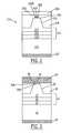
- FIG. 1is cross-sectional view illustrating a structure providing an ohmic contact to a P-type Group III-nitride based laser diode.
- a laser structure 210includes a substrate 212 on which is formed an epitaxial semiconductor structure 214 comprising one or more Group III-nitride materials.
- the epitaxial semiconductor structure 214may include an N-type layer 215 , a P-type layer 217 , and an active layer 216 between the N-type and P-type layers.
- the active layer 216may include any of a number of different structures and/or layers and/or combinations thereof, such as single or multiple quantum wells, double heterostructures, and/or superlattices. Active layer 216 may also include light and current confinement layers that may encourage laser action in the device.
- Portions of the epitaxial structure 214may be patterned into a mesa structure 220 for optical and current confinement purposes.
- a passivation layer 218may protect and insulate exposed surfaces of the P-type layer 217 .
- the passivation layer 218may be a layer of an insulating material such as silicon dioxide, silicon nitride, aluminum oxide, and/or combinations thereof.
- the laser structure 210may include a first ohmic contact layer 226 on the P-type layer 217 and a second ohmic contact layer 227 on the substrate 212 opposite the epitaxial semiconductor structure 214 .
- a metal overlayer 224may be provided on the passivation layer 218 and on the first ohmic contact layer 226 to provide a conductive path for interconnection of the device 210 with an external circuit.
- the metal overlayer 224may also provide some optical confinement for the device 210 .
- the ohmic contact 227may be provided on the N-type layer 215 .
- the substrate 212may comprise a conductive material such as N-type silicon carbide to provide a “vertical” device having a “vertical” current path between the first and second ohmic contacts 226 and 227 through the epitaxial semiconductor structure 214 and the substrate 212 .
- the anode and cathode of the deviceare on opposite sides of the substrate 212 .
- the second ohmic contactcould be placed on an exposed portion of the N-type layer 215 so that both ohmic contacts are on the same side of the substrate.
- the ohmic contact 226 on the P-type layer 217can be formed within a via 222 that has been opened through the passivation layer 218 to expose a portion of the surface 220 A of the mesa 220 .
- the mesa 220can be fabricated by forming an epitaxial semiconductor layer, forming a photoresist layer on the epitaxial semiconductor layer, patterning the photoresist layer to expose portions of the semiconductor layer (using a technique known as photolithography), and etching the exposed portions of the epitaxial semiconductor layer to form the mesa 220 .
- the epitaxial semiconductor structure 214 including the mesa 220is then covered with the passivation layer 218 , and a second patterned photoresist layer can be formed and patterned (using photolithography) on the passivation layer to expose a portion of the passivation layer where the via is to be formed.
- the exposed portion of the passivation layercan then be etched to form the via 222 exposing a portion of the mesa surface 220 A.
- a layer of a metal such as nickel, titanium, platinum, palladium, and/or combinations thereofcan then be deposited on the portion of the mesa surface 220 A exposed by the via 222 . Because of tolerance limits of the two photolithography steps discussed above, however, it may be difficult to align the via 222 with the mesa surface 220 A. Accordingly, the via 222 may need to be patterned to be significantly narrower than the mesa surface 220 A so that the passivation layer 218 may extend onto significant portions of the mesa surface 220 A and so that the ohmic contact 226 may not contact significant portions of the mesa surface 220 A. Accordingly, electric current passing from the ohmic contact 226 to the mesa surface 220 A may be distributed unevenly across the mesa and performance of the device may be degraded.
- a metalsuch as nickel, titanium, platinum, palladium, and/or combinations thereof
- the passivation layer 218may cover corners 211 of the mesa 220 .
- the corners 211may be electrically vulnerable regions of the structure, and the passivation layer may provide protection therefore. More particularly, it may be desirable to protect the mesa corners 211 when the metal overlayer 224 is deposited. If the corners are not protected when the metal overlayer 224 is deposited, metal from the overlayer may migrate down the mesa 220 sidewalls which may cause current leakage, electrical short circuits, and/or an increase in a lasing threshold voltage. Providing the passivation layer 218 on the corners 211 of the mesa 220 A may also protect mesa sidewalls from environmental conditions such as high humidity.
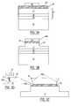
- a laser diode structure 30may include a substrate 12 and an epitaxial semiconductor structure 14 including semiconductor materials such as Group III-V semiconductor materials, and more particularly, semiconductor materials such as Group III-nitride semiconductor materials.
- the epitaxial semiconductor structure 14may include an N-type layer 15 and a P-type layer 17 .
- the epitaxial semiconductor structure 14may also include an active layer 16 between the N-type and P-type layers.
- the substrate 12may include a material such as N-type silicon carbide having a polytype such as 2H, 4H, 6H, 8H, 15R, and/or 3C; sapphire; gallium nitride; and/or aluminum nitride.
- a “vertical” devicecan be provided such that a current path is provided through the epitaxial semiconductor structure 14 and the substrate 12 .
- a “vertical” current pathis provided between the ohmic contact layers 36 and 27 which are provided on opposite sides of the substrate 12 .
- a “horizontal” devicemay be provided with both contacts on the same side of the substrate, in which case, the substrate may be insulating, semi-insulating, or conductive.
- the active layer 16may include a number of different structures and/or layers and/or combinations thereof.
- the active layer 16may include single or multiple quantum wells, double heterostructures, and/or superlattices.
- the active layer 16may also include light and/or current confinement layers that may encourage laser action in the device.
- Portions of the epitaxial semiconductor structure 14may be patterned into a semiconductor mesa 20 , for example, to provide optical and/or current confinement. As illustrated in FIG. 2, a portion of the P-type layer 17 may be included in the mesa 20 without including any of the N-type layer 15 in the mesa 20 . In alternatives, portions or all of the active layer 16 and or the N-type layer 15 may be included in the mesa 20 .
- a thickness of the mesa 20(determined, for example, by a depth of an etch used to form the mesa) may be in the range of approximately 0.1 to 5 microns, and more particularly, the thickness of the mesa may be less than approximately 2.5 microns.
- a width of the mesa surface 20 A(visible in the cross-section of FIG. 3) may be in the range of approximately 1 to 3 microns and a length of the mesa (perpendicular to the cross-section of FIG. 2) may be significantly greater.
- the ohmic contact 36may be formed on the mesa surface 20 A, and the ohmic contact 27 may be formed on the substrate 12 opposite the mesa 20 . As further shown in FIG. 2, the ohmic contact 36 may be in direct contact with substantially an entire width of the mesa surface 20 A.
- the passivation layer 34may protect and insulate exposed surfaces of the P-type layer 17 , and the passivation layer 34 may be a layer of an insulating material such as silicon dioxide, silicon nitride, aluminum oxide, and/or combinations thereof. Moreover, the passivation layer may be formed using a deposition technique such as plasma enhanced chemical vapor deposition (PECVD), low pressure chemical vapor deposition (LPCVD), chemical vapor deposition (CVD), sputtering, and/or e-beam evaporation. As shown, the passivation layer 34 may extend across peripheral portions of the mesa surface 20 A thereby covering potentially vulnerable corner portions of the mesa 20 where the mesa surface 20 A and mesa sidewalls meet.
- PECVDplasma enhanced chemical vapor deposition
- LPCVDlow pressure chemical vapor deposition
- CVDchemical vapor deposition
- sputteringand/or e-beam evaporation
- the passivation layer 34may also cover portions of beveled sidewalls of the ohmic contact layer 36 .
- Metal overlayer 24may include a layer of a metal such as nickel, gold, platinum, titanium, molybdenum, tantalum, palladium, and/or combinations thereof. As shown, the metal overlayer 24 can be in contact with the ohmic contact layer 36 to facilitate electrical connection of the laser diode with an external device.
- the ohmic contact layerfor example, may provide a surface for wire and/or other bonding for electrical connection with another device.
- a laser diode precursor structuremay include an epitaxial semiconductor structure 14 ′ including an N-type layer 15 and a P-type layer 17 ′.
- the epitaxial semiconductor layermay also include an active layer 16 between the N-type and P-type layers.
- a metal layer 42 ′may include a metal stack that provides ohmic contact with the epitaxial semiconductor structure 14 ′ opposite the substrate 12 .
- a metal stack of the metal layer 42 ′may also include other layers such as barrier and/or bonding layers as described, for example, in Published U.S. patent application Ser. No. 20/030,045,015 (Ser. No. 10/185,252) and Published U.S. patent application Ser. No. 20/030,042,507 (Ser. No. 10/185,350), the disclosures of which are hereby incorporated herein in their entirety by reference.
- a mask 44is provided on the metal layer 42 ′ to expose portions of the metal layer 42 ′ and the epitaxial semiconductor structure 14 ′.
- the mask 44may be a photoresist mask that is patterned using photolithographic techniques.
- the mask 44may be a layer of another material that can resist an etch chemistry used to etch the metal layer 42 ′ and the epitaxial semiconductor structure 14 ′.
- portions of the metal layer 42 ′ and the epitaxial semiconductor structure 14 ′ exposed by the mask 44can be selectively removed, for example, using a dry etch, to provide the ohmic contact layer 42 and the mesa 20 including portions of the P-type layer 17 .
- the mesa 20is shown exposing only portions of the P-type layer 17
- exposed portions of the epitaxial semiconductor structure 14 ′may be removed to a greater depth so that all of the P-type layer 17 is included in the mesa, so that all or portions of the active layer 16 are included in the mesa, and/or so that all or portions of the N-type layer 15 are included in the mesa.
- exposed portions of the metal layer 42 ′ and the epitaxial semiconductor structure 14 ′can be removed down to the substrate 12 .
- Exposed portions of the metal layer 42 ′ and the epitaxial semiconductor structure 14 ′can be removed using a dry etch such as a Reactive Ion Etch (RIE), an Electron Cyclotron Resonance (ECR) plasma etch, and/or an Inductively Coupled Plasma (ICP) etch. More particularly, the metal layer and the epitaxial semiconductor layer can be etched using a dry etch in an Argon (Ar) environment with a chlorine (Cl 2 ) etchant.
- RIEReactive Ion Etch
- ECRElectron Cyclotron Resonance
- ICPInductively Coupled Plasma
- argoncan flow at a rate in the range of approximately 2 to 40 sccm and chlorine can flow at a rate in the range of approximately 5 to 50 sccm in an RIE reactor at a pressure in the range of approximately 5 to 50 mTorr and at an RF power in the range of approximately 200 to 1000 W.
- etch parametersare provided by way of example, and other etch parameters may be used.
- FIGS. 3C and 3Dillustrate the intersection of the ohmic contact layer 42 and the mask 44 in greater detail after completion of the mesa etch.
- residue 45may build up on sidewalls 44 A of the mask 44 as the etch progresses through the metal layer 42 ′ to form the ohmic contact layer 42 .
- the residue 45may result from redeposition of material etched from the metal layer 42 ′. More particularly, when dry etching the metal layer 42 ′, the metal layer 42 ′ may be bombarded with reactive ions 41 as shown in FIG. 3D, and the reactive ions 41 may physically remove exposed portions of the metal layer 42 ′.
- Etch by-products such as ions 41 and/or etched materialmay form a residue 45 that builds up on sidewalls of the mask 44 as the etch of the metal layer 42 ′ progresses. Because the residue 45 may effectively increase a width of the mask 44 as the etch progresses through the metal layer 42 ′, an increasing area of the metal layer 42 ′ may be shielded/shadowed from the etch as the depth of the etch increases. Accordingly, sidewalls 42 A of the ohmic contact layer 42 may be inwardly beveled or slanted.
- a passivation layer 34is formed on exposed portions of the P-type layer 17 , on the mask 34 , and on portions of the beveled sidewalls of the ohmic contact layer 42 .
- the passivation layer 34may include a layer of an insulting material such as silicon nitride, silicon dioxide, and/or aluminum oxide.
- the passivation layer 34may be formed using a deposition technique such as plasma enhanced chemical vapor deposition (PECVD), low pressure chemical vapor deposition (LPCVD), chemical vapor deposition (CVD), sputtering, and/or e-beam evaporation.
- PECVDplasma enhanced chemical vapor deposition
- LPCVDlow pressure chemical vapor deposition
- CVDchemical vapor deposition
- sputteringand/or e-beam evaporation.
- the passivation layer 34may have a thickness that is slightly greater than a depth of the etch into the semiconductor layer.
- the passivation layer 34may have a thickness in the range of approximately 0.1 to 2 microns with the etch depth into the semiconductor layer being slightly less than the thickness of the passivation layer.
- portions 38 of the passivation layer 34 on the inwardly beveled sidewalls of the ohmic contact layer 42may cover corner portions of the semiconductor mesa 20 .
- the portions 38 of the passivation layer 34may thus provide electrical and/or physical protection for the corner portions of the semiconductor mesa 20 .
- the mask 44 and portions of the passivation layer 34 on the maskcan then be removed using a lift-off technique, and the resulting structure can be rinsed in de-ionized water.
- Portions 38 of the passivation layer 34 that overlap the semiconductor mesa 20may thus effectively provide a self-aligned via surrounding and protecting the ohmic contact layer 42 .
- the same mask that is used to pattern the ohmic contact layer 42 and the semiconductor mesa 20is also used to define a contact surface of the ohmic contact layer that is exposed through the passivation layer.
- a metal overlayer 50can then be deposited on the passivation layer 34 and on exposed portions of the ohmic contact layer 42 as shown in FIG. 3F.
- the metal overlayermay be a layer of a metal such as nickel, gold, platinum, titanium, tungsten, molybdenum, tantalum, palladium, and/or combinations thereof.
- Portions 38 of the passivation layer 34may thus define a self-aligned via to allow contact between the ohmic contact layer 42 and the metal overlayer 50 while reducing the possibility of contact between the metal overlayer 50 and the P-type layer.
- leakage currents, short circuits, and/or threshold voltagesmay be reduced.
- FIG. 4is a photograph illustrating mesa structures according to embodiments of the present invention.
- a semiconductor devicecan include a substrate 112 , and a semiconductor structure 114 on the substrate 112 with the semiconductor structure 114 including a semiconductor mesa 120 having semiconductor mesa sidewalls 120 A and a semiconductor mesa surface 120 B opposite the substrate 112 .
- An ohmic contact layer 136 on the semiconductor mesa surface 120 Bcan include sidewalls 136 A and a contact surface 136 B opposite the semiconductor mesa surface 120 B, and the ohmic contact layer 136 can extend substantially across an entirety of the semiconductor mesa surface 120 B.
- a passivation layer 134can be provided on the semiconductor mesa sidewalls 120 A and on portions of the ohmic contact layer sidewalls 136 A adjacent the semiconductor mesa surface 120 B, and the passivation layer 134 can expose substantially an entirety of the contact surface 136 B of the ohmic contact layer 136 . Portions of the ohmic contact layer sidewalls 136 A adjacent the contact surface 136 B may also be exposed by the passivation layer 134 .
- the ohmic contact layer sidewalls 136 Acan be inwardly beveled, and the passivation layer 134 may extend onto the inwardly beveled sidewalls of the ohmic contact layer adjacent the semiconductor mesa sidewalls 120 A. Portions of the ohmic contact layer sidewalls 136 A adjacent the semiconductor mesa surface 120 B may be covered by the passivation layer 134 , and portions of the ohmic contact layer sidewalls 136 A adjacent the contact surface 136 B may be free of the passivation layer 134 .
- the semiconductor mesa sidewalls 120 A of the semiconductor structure 114may have a first slope relative to the substrate and the ohmic contact layer sidewalls 136 A may have a second slope relative to the substrate wherein the second slope is less than the first slope.
- the passivation layercan protect corner portions of the semiconductor mesa 120 between the semiconductor mesa sidewalls 120 A and the semiconductor mesa surface 120 B.
- the semiconductor devicecan also include a conductive overlayer 124 on the passivation layer 134 and on exposed portions of the ohmic contact layer 136 . More particularly, the conductive overlayer 124 can provide electrical contact with the contact surface 136 B and exposed portions of the ohmic contact layer sidewalls 136 A to provide a current path through the semiconductor mesa 120 of the semiconductor structure 114 .
- a second contact layer 127can be provided on the substrate 112 opposite the semiconductor structure 114 so that a “vertical” current path is defined between the conductive overlayer 124 and the second contact layer 127 through the ohmic contact layer 136 , the semiconductor structure 114 , and the substrate 112 .
- a second contact layermay be provided on a surface of the substrate 112 adjacent the semiconductor structure 114 or on a surface of the semiconductor structure 114 adjacent the semiconductor mesa to define a “horizontal” current path.
- the semiconductor structure 114may include a first layer of a first conductivity type and a second layer of a second conductivity type on the first layer opposite the substrate 112 .
- the first layermay be an N-type layer and the second layer may be a P-type layer so that a P—N junction is defined therebetween.
- the semiconductor devicemay be a light emitting device so that light is emitted responsive to electrical current passing through the P—N junction. More particularly, the semiconductor device may be a semiconductor laser so that coherent light is emitted from the semiconductor mesa structure 114 parallel to the substrate and perpendicular to the plane of the cross-section.
- the semiconductor mesa sidewalls 120 Amay expose portions of the second layer of the second conductivity type without exposing portions of the first layer of the first conductivity type. Accordingly, the P—N junction can be located in the semiconductor structure 114 below the semiconductor mesa 120 . In an alternative, the semiconductor mesa sidewalls 120 A may expose portions of both the first layer of the first conductivity type and the second layer of the second conductivity type. Accordingly, the P—N junction can be located in the semiconductor mesa 120 of the semiconductor structure 114 .
- the semiconductor structure 114can also include an active layer between the first and second layers of the first and second conductivity types.
- An active layermay include different structures and/or layers an/or combinations thereof, such as single or multiple quantum wells, double heterostructures, and/or superlattices.
- An active layermay also include light and/or current confinement layers that may encourage laser action in the device.
- portions of the semiconductor structure 114 included in the semiconductor mesa 120may have a thickness in the range of approximately 0.1 to 5 microns. According to additional embodiments of the present invention, portions of the semiconductor structure 114 included in the semiconductor mesa 120 have a thickness of less than approximately 2.5 microns.
- the semiconductor mesa surface 120 B of the semiconductor structure 114can have a width in the range of approximately 1 to 3 microns where the width is the lateral dimension of the semiconductor mesa surface 120 B visible in the cross-section of FIG. 5.
- the length of the mesa 120is the dimension of the mesa perpendicular to the cross-section of FIG. 5, and the length of the mesa may be significantly greater than the width. By providing the length significantly greater than the width, the mesa may provide current and/or optical confinement when providing a semiconductor laser device.
- the semiconductor structure 114may have a semiconductor mesa 120 and a non-patterned portion between the semiconductor mesa 120 and the substrate 112 so that at least a portion of the first layer of the first conductivity type is not included in the semiconductor mesa 120 .
- the semiconductor mesa sidewalls 120 Amay extend from the semiconductor mesa surface 120 B to the substrate 112 so that all of the first layer of the first conductivity type is included in the semiconductor mesa 120 .
- the semiconductor structure 114may comprise a Group III-V semiconductor material such as a Group III-nitride semiconductor material.
- the substrate 112may comprise N-type silicon carbide having a polytype selected from 2H, 4H, 6H, 8H, 15R, and/or 3C.
- the substratecould alternately comprise another material such as sapphire, gallium nitride, and/or aluminum nitride.
- the substrate 112may be conductive when the second contact layer 127 is provided on a side thereof opposite the semiconductor structure 114 . Non-conductive substrate materials, however, may be used if a current path is not provided through the substrate 112 .
- the term substratemay be defined to include a non-patterned portion of the semiconductor material making up the semiconductor structure 114 , and/or there may not be a material transition between the substrate 112 and the semiconductor structure 114 .
- the semiconductor structuremay be an epitaxial semiconductor structure.
- the conductive overlayer 124may be a metal layer such as a layer of nickel (Ni), gold (Au), platinum (Pt), titanium (Ti), tungsten (W), molybdenum (Mo), tantalum (Ta), and/or palladium (Pd).
- the passivation layermay be a layer of an insulating material such as a layer of silicon nitride, silicon oxide, and/or aluminum oxide.
- the passivation layermay be formed using one or more of chemical vapor deposition (CVD), plasma enhanced chemical vapor deposition (PECVD), low pressure chemical vapor deposition (LPCVD), sputtering, and/or e-beam evaporation.
- CVDchemical vapor deposition
- PECVDplasma enhanced chemical vapor deposition
- LPCVDlow pressure chemical vapor deposition
- sputteringand/or e-beam evaporation.
- FIGS. 6 A- 6 Dillustrate steps of forming the semiconductor device illustrated in FIG. 5.
- a semiconductor layer 114 ′may be formed on a substrate 112
- a conductive layer 136 ′may be formed on the semiconductor layer 114 ′ opposite the substrate 112
- a mask 144may be formed on the conductive layer 136 ′ opposite the semiconductor layer 114 ′.
- the substratemay comprise a material such as N-type silicon carbide substrate having a polytype such as 2H, 4H, 6H, 8H, 15R, and 3C; sapphire; gallium nitride; and/or aluminum.
- the conductive layer 136 ′may comprise a metal such as nickel, titanium, platinum, and/or palladium, and the mask 144 may be a photoresist mask or other masking material that can resist an etch used to pattern the conductive layer 136 ′ and the semiconductor layer 114 ′.
- the semiconductor layer 114 ′may comprise a semiconductor material such as a Group III-V semiconductor material, and more particularly a Group III-nitride material. Moreover, the semiconductor material may comprise a first layer of a first conductivity type and a second layer of a second conductivity type on the first layer opposite the substrate. More particularly, the first layer may be an N-type semiconductor layer on the substrate 112 , and the second layer may be a P-type semiconductor layer on the N-type semiconductor layer opposite the substrate so that a P—N junction is defined therebetween. Moreover, forming the semiconductor layer may include forming an epitaxial semiconductor layer.
- the semiconductor layermay include an active layer between the N-type and P-type layers.
- An active layermay include different structures and/or layers an/or combinations thereof, such as single or multiple quantum wells, double heterostructures, and/or superlattices.
- An active layermay also include light and/or current confinement layers that may encourage laser action in the device.
- portions of the conductive layer 136 ′ and the semiconductor layer 114 ′ exposed by the mask 144are selectively removed to define the ohmic contact layer 136 and the semiconductor structure 114 including a semiconductor mesa 120 having semiconductor mesa sidewalls 120 A and a semiconductor mesa surface 120 B.
- Portions of the conductive layer and the semiconductor layercan be selectively removed using a dry etch such as a Reactive Ion Etch (RIE), an Electron Cyclotron Resonance (ECR) plasma etch, and/or an Inductively Coupled Plasma (ICP) etch.
- RIEReactive Ion Etch
- ECRElectron Cyclotron Resonance
- ICPInductively Coupled Plasma
- the semiconductor layermay be etched using a dry etch in a Argon (Ar) environment with a chlorine (Cl 2 ) etchant. More particularly, the dry etch may be performed by flowing Ar at a flow in the range of approximately 2-40 sccm and flowing Cl 2 at a flow in the range of approximately 5-50 sccm in an RIE reactor at a pressure in the range of approximately 5-50 mTorr and at a radio frequency (RF) power in the range of approximately 200-1000W.
- ArArgon
- Cl 2chlorine
- RFradio frequency
- the semiconductor layer 144 ′may be etched to at depth in the range of approximately 0.1 to 5 microns. According to additional embodiments of the present invention, the semiconductor layer 144 ′ may be etched to a depth of less than approximately 2.5 microns. The depth of the etch will determine the thickness of the semiconductor mesa 120 . As discussed above, the semiconductor layer 114 ′ may include a first conductivity-type layer (such as an N-type layer) on the substrate and a second conductivity-type layer (such as a P-type layer) on the first conductivity-type layer opposite the substrate.
- a first conductivity-type layersuch as an N-type layer
- a second conductivity-type layersuch as a P-type layer
- the etch depthmay be such that only portions of the second conductivity-type layer are exposed along the resulting mesa sidewalls 120 A. In an alternative, the etch depth may be such that portions of the first conductivity-type layer are also exposed along the resulting mesa sidewalls 120 A. While the etch is shown extending through only a portion of the thickness of the semiconductor layer 114 ′, the etch could extend through the entire thickness of the semiconductor layer so that portions of the substrate 112 are exposed adjacent the mesa sidewalls 120 A. Moreover, the mask 144 can be provided so that the mesa surface 120 B has a width in the range of approximately 1 to 3 microns.
- a residue 144 ′may build up on sidewalls of the mask 144 as a dry etch progresses through the conductive layer 136 ′. More particularly, portions of the conductive layer 136 ′ may be physically removed by bombarding electrons during a dry etch, and some of this removed material may generate the residue that builds up on sidewalls of the mask. Because the residue builds over time, a greater portion of the conductive layer may be shielded from the etch as the etch depth increases so that the sidewalls 136 A of the ohmic contact layer 136 are inwardly beveled.
- etching of the semiconductor layer 114 ′may result in reduced generation of etch residue on the mask sidewalls so that the slopes of the semiconductor mesa sidewalls 120 A may be greater than the slopes of the ohmic contact layer sidewalls 136 A.
- the ohmic contact layer 136 and the semiconductor mesa 120are patterned at the same time, the ohmic contact layer 136 can provide coverage across substantially an entirety of the semiconductor mesa surface 120 B without extending onto mesa sidewalls 120 B.
- the ohmic contact layer 136can thus be “self aligned” with respect to the semiconductor surface 120 B. Accordingly, improved current spreading can be provided for an electronic device with a current flow through the mesa surface.
- the ohmic contact layer 136may provide improved protection for corners of the semiconductor mesa 120 .
- a passivation layer 134can be formed on sidewalls 120 A of the semiconductor mesa 120 and on the mask 144 . Stated in other words, the mask 144 is maintained-while forming the passivation layer. The passivation layer may also be formed on portions the ohmic contact layer sidewalls 136 A adjacent the semiconductor mesa surface 120 B. Because the mask is maintained while forming the passivation layer, the passivation layer is not formed directly on the contact surface 136 B of the ohmic contact layer. Due to shielding of the residue 144 ′, portions of the ohmic contact layer sidewalls 136 A adjacent the contact surface 136 B may also be maintained free of the passivation layer. By providing the passivation layer on portions of the inwardly beveled sidewalls 136 A of the ohmic contact layer 136 , additional protection may be provided for corners of the semiconductor mesa 120 .
- the passivation layer 134may be a layer of an insulting material such as silicon nitride, silicon oxide, and/or aluminum oxide. Moreover, the passivation layer may be formed using chemical vapor deposition (CVD), plasma enhanced chemical vapor deposition (PECVD), low pressure chemical vapor deposition (LPCVD), sputtering, and/or e-beam evaporation. According to embodiments of the present invention, the passivation layer is formed to have a thickness greater than a thickness of the semiconductor mesa 120 (i.e. a depth of the etch into the semiconductor layer 144 ′) but less than a combined thickness of the semiconductor mesa 120 and the ohmic contact layer 136 .
- CVDchemical vapor deposition
- PECVDplasma enhanced chemical vapor deposition
- LPCVDlow pressure chemical vapor deposition
- sputteringand/or e-beam evaporation.
- the passivation layeris formed to have a thickness greater than a thickness of the
- the passivation layermay cover the semiconductor mesa sidewalls 120 A and portions of the ohmic contact layer sidewalls 136 A, but the ohmic contact surface 136 B may still extend through the passivation layer.
- the passivation layermay have a thickness in the range of approximately 0.1 to 2.0 microns with the thickness of the semiconductor mesa 120 being slightly less.
- the mask 144 and portions of the passivation layer 134 on the maskcan then be removed thereby exposing the contact surface 136 B of the ohmic contact layer 136 , for example, using a lift-off technique.
- the contact surface 136 Bcan thus be exposed through the passivation layer without using a separate masking step to form a via through the passivation layer.
- the passivation layercan be “self aligned” with respect to the ohmic contact layer.
- a conductive overlayer 124is then formed on the contact surface 136 B and on portions of the passivation layer 134 surrounding the ohmic contact layer 136 .
- the conductive overlayer 124may comprise a metal such as nickel (Ni), gold (Au), platinum (Pt), titanium (Ti), tungsten (W), molybdenum (Mo), tantalum (Ta), and/or palladium (Pd).
- the conductive overlayermay provide a large area contact for a wire bond or other interconnection.
- a second ohmic contact 127may be provided on the substrate 112 opposite the semiconductor mesa 120 . While the second ohmic contact is shown as being formed after forming the semiconductor mesa 120 , the second ohmic contact 127 may be formed at any point during the fabrication of the semiconductor device. With the second ohmic contact provided on the substrate opposite the semiconductor device, a “vertical” current path may be provided through the semiconductor mesa and the substrate. In an alternative, a second ohmic contact may be provided on a surface of the substrate adjacent the semiconductor mesa, or a second ohmic contact may be formed on a portion of the semiconductor layer 114 opposite the substrate to provide a “horizontal” current path.
- the resulting semiconductor devicemay provide an edge emitting semiconductor laser with light being emitted parallel to the substrate along a lengthwise direction of a semiconductor mesa stripe. Stated in other words, the light may be emitted along a direction perpendicular to the cross section of FIG. 6D. While methods and devices have been discussed with reference to methods of forming light emitting devices such as laser diodes, methods according to embodiments of the present invention may be used to form other semiconductor devices such as conventional diodes, conventional light emitting diodes, or any other semiconductor device including a semiconductor mesa.
Landscapes
- Physics & Mathematics (AREA)
- Condensed Matter Physics & Semiconductors (AREA)
- General Physics & Mathematics (AREA)
- Electromagnetism (AREA)
- Optics & Photonics (AREA)
- Geometry (AREA)
- Semiconductor Lasers (AREA)
- Bipolar Transistors (AREA)
- Formation Of Insulating Films (AREA)
- Electrodes Of Semiconductors (AREA)
- Light Receiving Elements (AREA)
- Internal Circuitry In Semiconductor Integrated Circuit Devices (AREA)
- Led Devices (AREA)
- Insulated Gate Type Field-Effect Transistor (AREA)
Abstract
Description
- The present application claims the benefit of: U.S. Provisional Application No. 60/435,213 filed Dec. 20, 2002, and entitled “Laser Diode With Self-Aligned Index Guide And Via”; U.S. Provisional Application No. 60/434,914 filed Dec. 20, 2002, and entitled “Laser Diode With Surface Depressed Ridge Waveguide”; U.S. Provisional Application No. 60/434,999 filed Dec. 20, 2002 and entitled “Laser Diode with Etched Mesa Structure”; and U.S. Provisional Application No. 60/435,211 filed Dec. 20, 2002, and entitled “Laser Diode With Metal Current Spreading Layer.” The disclosures of each of these provisional applications are hereby incorporated herein in their entirety by reference.[0001]
- The present application is also related to: U.S. application Ser. No. ______ (Attorney Docket No. 5308-280) entitled “Methods Of Forming Semiconductor Mesa Structures Including Self-Aligned Contact Layers And Related Devices” filed concurrently herewith; U.S. application Ser. No. ______ (Attorney Docket No. 5308-282) entitled “Methods Of Forming Semiconductor Devices Including Mesa Structures And Multiple Passivation Layers And Related Devices” filed concurrently herewith; and U.S. application Ser. No. ______ (Attorney Docket No. 5308-283) entitled “Methods Of Forming Electronic Devices Including Semiconductor Mesa Structures And Conductivity Junctions And Related Devices” filed concurrently herewith. The disclosures of each of these U.S. applications are hereby incorporated herein in their entirety by reference.[0002]
- The present invention relates to the field of electronics, and more particularly, to methods of forming electronic semiconductor devices and related structures.[0003]
- A laser is a device that produces a beam of coherent monochromatic light as a result of stimulated emission of photons. Stimulated emission of photons may also produce optical gain, which may cause light beams produced by lasers to have a high optical energy. A number of materials are capable of producing the lasing effect and include certain high-purity crystals (ruby is a common example), semiconductors, certain types of glass, certain gases including carbon dioxide, helium, argon and neon, and certain plasmas.[0004]
- More recently, lasers have been developed in semiconducting materials, thus taking advantage of the smaller size, lower cost and other related advantages typically associated with semiconductor devices. In the semiconductor arts, devices in which photons play a major role are referred to as “photonic” or “optoelectronic” devices. In turn, photonic devices include light-emitting diodes (LEDs), photodetectors, photovoltaic devices, and semiconductor lasers.[0005]
- Semiconductor lasers are similar to other lasers in that the emitted radiation has spatial and temporal coherence. As noted above, laser radiation is highly monochromatic (i.e., of narrow band width) and it produces highly directional beams of light. Semiconductor lasers may differ, however, from other lasers in several respects. For example, in semiconductor lasers, the quantum transitions are associated with the band properties of materials; semiconductor lasers may be very compact in size, may have very narrow active regions, and larger divergence of the laser beam; the characteristics of a semiconductor laser may be strongly influenced by the properties of the junction medium; and for P—N junction lasers, the lasing action is produced by passing a forward current through the diode itself. Overall, semiconductor lasers can provide very efficient systems that may be controlled by modulating the current directed across the devices. Additionally, because semiconductor lasers can have very short photon lifetimes, they may be used to produce high-frequency modulation. In turn, the compact size and capability for such high-frequency modulation may make semiconductor lasers an important light source for optical fiber communications.[0006]
- In broad terms, the structure of a semiconductor laser should provide optical confinement to create a resonant cavity in which light amplification may occur, and electrical confinement to produce high current densities to cause stimulated emission to occur. Additionally, to produce the laser effect (stimulated emission of radiation), the semiconductor may be a direct bandgap material rather than an indirect bandgap material. As known to those familiar with semiconductor characteristics, a direct bandgap material is one in which an electron's transition from the valence band to the conduction band does not require a change in crystal momentum for the electron. Gallium arsenide and gallium nitride are examples of direct bandgap semiconductors. In indirect bandgap semiconductors, the alternative situation exists; i.e., a change of crystal momentum is required for an electron's transition between the valence and conduction bands. Silicon and silicon carbide are examples of such indirect semiconductors.[0007]
- A useful explanation of the theory, structure and operation of semiconductor lasers, including optical and electronic confinement and mirroring, is given by Sze, Physics of Semiconductor Devices, 2nd Edition (1981) at pages 704-742, and these pages are incorporated entirely herein by reference.[0008]
- As known to those familiar with photonic devices such as LEDs and lasers, the frequency of electromagnetic radiation (i.e., the photons) that can be produced by a given semiconductor material may be a function of the material's bandgap. Smaller bandgaps produce lower energy, longer wavelength photons, while wider bandgap materials produce higher energy, shorter wavelength photons. For example, one semiconductor commonly used for lasers is aluminum indium gallium phosphide (AlInGaP). Because of this material's bandgap (actually a range of bandgaps depending upon the mole or atomic fraction of each element present), the light that AlInGaP can produce may be limited to the red portion of the visible spectrum, i.e., about 600 to 700 nanometers (nm). In order to produce photons that have wavelengths in the blue or ultraviolet portions of the spectrum, semiconductor materials having relatively large bandgaps may be used. Group III-nitride materials such as gallium nitride (GaN), the ternary alloys indium gallium nitride (InGaN), aluminum gallium nitride (AlGaN) and aluminum indium nitride (AlInN) as well as the quaternary alloy aluminum gallium indium nitride (AlInGaN) are attractive candidate materials for blue and UV lasers because of their relatively high bandgap (3.36 eV at room temperature for GaN). Accordingly, Group III-nitride based laser diodes have been demonstrated that emit light in the 370-420 nm range.[0009]
- A number of commonly assigned patents and co-pending patent applications likewise discuss the design and manufacture of optoelectronic devices. For example, U.S. Pat. Nos. 6,459,100; 6,373,077; 6,201,262; 6,187,606; 5,912,477; and 5,416,342 describe various methods and structures for gallium-nitride based optoelectronic devices. U.S. Pat. No. 5,838,706 describes low-strain nitride laser diode structures. Published U.S. application Ser. Nos. 20/020,093,020 and 20/020,022,290 describe epitaxial structures for nitride-based optoelectronic devices. Various metal contact structures and bonding methods, including flip-chip bonding methods, are described in Published U.S. application Ser. No. 20/020,123,164 as well as Published U.S. application Ser. No. 03/0,045,015 entitled “Flip Chip Bonding of Light Emitting Devices and Light Emitting Devices Suitable for Flip-Chip Bonding”; Published U.S. application Ser. No. 20/030,042,507 entitled “Bonding of Light Emitting Diodes Having Shaped Substrates and Collets for Bonding of Light Emitting Diodes Having Shaped Substrates”, and Published U.S. application Ser. No. 20/030,015,721 entitled “Light Emitting Diodes Including Modifications for Submount Bonding and Manufacturing Methods Therefor.” Dry etching methods are described in U.S. Pat. No. 6,475,889. Passivation methods for nitride optoelectronic devices are described in U.S. application Ser. No. 08/920,409 entitled “Robust Group III Light Emitting Diode for High Reliability in Standard Packaging Applications” and Published U.S. application Ser. No. 20/030,025,121 entitled “Robust Group III Light Emitting Diode for High Reliability in Standard Packaging Applications.” Active layer structures suitable for use in nitride laser diodes are described in Published U.S. application Ser. No. 20/030,006,418 entitled “Group III Nitride Based Light Emitting Diode Structures with a Quantum Well and Superlattice, Group III Nitride Based Quantum Well Structures and Group III Nitride Based Superlattice Structures” and Published U.S. application Ser. No. 20/030,020,061 entitled “Ultraviolet Light Emitting Diode.” The contents of all of the foregoing patents, patent applications and published patent applications are incorporated entirely herein by reference as if fully set forth herein.[0010]
- Vulnerable portions of conventional semiconductor laser devices, however, may be subject to damage during fabrication and/or subsequent packaging. Moreover, electrically vulnerable portions of conventional semiconductor laser devices may result in current leakage, electrical short circuits, and/or increased lasing thresholds.[0011]
- According to embodiments of the present invention, methods of forming semiconductor devices may include forming a semiconductor layer on a substrate, forming a conductive layer on the semiconductor layer opposite the substrate, and forming a mask on the conductive layer opposite the semiconductor layer. Portions of the conductive layer and the semiconductor layer exposed by the mask may be selectively removed while maintaining the mask to define a semiconductor mesa having mesa sidewalls between the mask and the substrate and a mesa surface opposite the substrate and defining a contact layer on the mesa surface between the semiconductor mesa and the mask. A passivation layer can be formed on the mask and on the mesa sidewalls, and the mask and portions of the passivation layer on the mask can be removed. More particularly, the contact layer may provide ohmic contact with the semiconductor mesa.[0012]
- While selectively removing portions of the metal layer, by-products of the conductive layer may be redeposited on sidewalls of the mask. Accordingly, an effective width of the mask may increase as the conductive layer is removed. In addition, the mesa may be configured to provide at least one of optical confinement or current confinement for a light emitting device in the semiconductor structure. Moreover, the mesa sidewalls may be free of the conductive contact layer.[0013]
- The semiconductor layer can be a Group III-V semiconductor material such as a Group III-nitride semiconductor material, and forming the semiconductor layer may include forming an epitaxial semiconductor layer. Moreover, the semiconductor layer may include a first layer of a first conductivity type (such as N-type) and a second layer of a second conductivity type (such as P-type) on the first layer opposite the substrate. More particularly, removing portions of the semiconductor layer may include removing portions of the second layer of the second conductivity type without removing portions of the first layer of the first conductivity type. In an alternative, removing portions of the semiconductor layer may include removing portions of the first and second layers. In addition, the semiconductor layer may include an active layer between the first and second layers.[0014]
- Portions of the semiconductor layer included in the mesa may have a thickness in the range of approximately 0.1 to 5 microns or more, and more particularly, portions of the semiconductor layer included in the mesa may have a thickness of less than approximately 2.5 microns. In addition, the mesa surface may have a width in the range of approximately 1 to 3 microns or more at an interface with the contact layer.[0015]
- After removing the mask and portions of the passivation layer on the mask, methods according to embodiments of the present invention may also include forming a conductive overlayer on the mesa surface and on portions of the passivation layer surrounding the contact layer. The conductive overlayer may include a metal layer such as a layer of nickel (Ni), gold (Au), platinum (Pt), titanium (Ti), tungsten (W), molybdenum (Mo), tantalum (Ta), and/or palladium (Pd). The passivation layer may include an insulating layer such as a layer of silicon nitride, silicon oxide, and/or aluminum oxide. Moreover, forming the passivation layer may include depositing the passivation layer using chemical vapor deposition (CVD), plasma enhanced chemical vapor deposition (PECVD), low pressure chemical vapor deposition (LPCVD), sputtering, and/or e-beam evaporation.[0016]
- The contact layer may include inwardly beveled sidewalls and a contact surface opposite the mesa surface, wherein the passivation layer extends onto the inwardly beveled sidewalls of the contact layer, and wherein the contact surface of the contact layer is free of the passivation layer. In addition, portions of the inwardly beveled sidewalls adjacent the contact surface may be free of the passivation layer. Sidewalls of the semiconductor mesa may have a first slope relative to the substrate, and sidewalls of the contact layer may have a second slope relative to the substrate, and the first slope can be greater than the second slope. In addition, selectively removing portions of the conductive layer and the semiconductor layer may include dry etching portions of the conductive layer and the semiconductor layer.[0017]
- According to additional embodiments of the present invention, methods of forming semiconductor devices may include forming a semiconductor structure on a substrate wherein the semiconductor structure has mesa sidewalls and a mesa surface opposite the substrate. A contact layer is formed on the mesa surface wherein the contact layer has sidewalls and a contact surface opposite the mesa surface and the contact layer may extend substantially across an entirety of the mesa surface. A passivation layer is formed on the mesa sidewalls and on portions of the contact layer sidewalls adjacent the mesa surface, and the passivation layer exposes substantially an entirety of the contact surface of the contact layer.[0018]
- The semiconductor structure may comprise a Group III-V semiconductor material such as a Group III-nitride semiconductor material. In addition, the semiconductor structure may include a first layer of a first conductivity type (such as N-type) and a second layer of a second conductivity type (such as P-type) on the first layer opposite the substrate. The mesa sidewalls may expose portions of the second layer of the second conductivity type without exposing portions of the first layer of the first conductivity type. In an alternative, the mesa sidewalls may expose portions of the first layer of the first conductivity type and portions of the second layer of the second conductivity type. The semiconductor structure may also include an active layer between the first and second layers.[0019]
- Portions of the semiconductor structure included in the mesa may have a thickness in the range of approximately 0.1 to 5 microns, and more particularly, portions of the semiconductor structure included in the mesa have a thickness of less than approximately 2.5 microns. In addition, the mesa surface of the semiconductor structure may have a width in the range of approximately 1 to 3 microns.[0020]
- Methods according to embodiments of the present invention may include forming a conductive overlayer on the exposed portions of the contact layer and on portions of the passivation layer surrounding the contact layer. The conductive overlayer comprises a metal layer such as a layer of nickel (Ni), gold (Au), platinum (Pt), titanium (Ti), tungsten (W), molybdenum (Mo), tantalum (Ta), and/or palladium (Pd). The passivation layer may include a layer of an insulating material such as silicon nitride, silicon oxide, and/or aluminum oxide. Moreover, forming the passivation layer may include depositing the passivation layer using chemical vapor deposition (CVD), plasma enhanced chemical vapor deposition (PECVD), low pressure chemical vapor deposition (LPCVD), sputtering, and/or e-beam evaporation.[0021]
- The contact layer sidewalls may be inwardly beveled with the passivation layer extending onto the inwardly beveled sidewalls of the contact layer opposite the mesa surface. In addition or in an alternative, the mesa sidewalls of the semiconductor structure may have a first slope relative to the substrate and the contact layer sidewalls may have a second slope relative to the substrate wherein the second slope is less than the first slope.[0022]
- Before forming the passivation layer, a mask can be maintained on the contact layer opposite the semiconductor substrate and forming the passivation layer can include forming the passivation layer on the mask. After forming the passivation layer, the mask and portions of the passivation layer on the mask can be removed. Accordingly, the contact surface of the contact layer can be maintained free of the passivation layer without using a masking operation to form a via hole through the passivation layer. In addition, forming the semiconductor structure and forming the contact layer may include forming a semiconductor layer on the substrate, forming a conductive layer on the semiconductor layer, and forming the mask on the conductive layer opposite the semiconductor layer. Portions of the conductive layer and the semiconductor layer exposed by the mask can then be removed to form the contact layer and the semiconductor structure. The passivation layer may also expose portions of the contact layer sidewalls adjacent the contact surface.[0023]
- According to yet additional embodiment of the present invention, a semiconductor device may include a substrate, and a semiconductor structure on the substrate, the semiconductor structure having mesa sidewalls and a mesa surface opposite the substrate. A contact layer on the mesa surface has sidewalls and a contact surface opposite the mesa surface, and the contact layer extends substantially across an entirety of the mesa surface. A passivation layer is on the mesa sidewalls and on portions of the contact layer sidewalls adjacent the mesa surface, and the passivation layer exposes substantially an entirety of the contact surface of the contact layer.[0024]
- The semiconductor structure may include a Group III-V semiconductor material such as a Group III-nitride semiconductor material. The semiconductor structure may include a first layer of a first conductivity type (such as N-type) and a second layer of a second conductivity type (such as P-type) on the first layer opposite the substrate. In addition, the mesa sidewalls may expose portions of the second layer of the second conductivity type without exposing portions of the first layer of the first conductivity type. In an alternative, the mesa sidewalls may expose portions of the first layer of the first conductivity type and portions of the second layer of the second conductivity type. The semiconductor structure may also include an active layer between the first and second layers.[0025]
- Portions of the semiconductor structure included in the mesa may have a thickness in the range of approximately 0.1 to 5 microns, and more particularly, portions of the semiconductor structure included in the mesa may have a thickness of less than approximately 2.5 microns. The mesa surface of the semiconductor structure may have a width in the range of approximately 1 to 3 microns.[0026]
- The semiconductor device may also include a conductive overlayer on the exposed portions of the contact layer and on portions of the passivation layer surrounding the contact layer. The conductive overlayer may include a metal layer such as a layer of nickel (Ni), gold (Au), platinum (Pt), titanium (Ti), tungsten (W), molybdenum (Mo), tantalum (Ta), and/or palladium (Pd). The passivation layer may include a layer of an insulting material such as silicon nitride, silicon oxide, and/or aluminum oxide.[0027]
- The contact layer sidewalls may be inwardly beveled and the passivation layer may extend onto the inwardly beveled sidewalls of the contact layer opposite the mesa surface. Moreover, the passivation layer may expose portions of the contact layer sidewalls adjacent the contact surface. In addition, the mesa sidewalls of the semiconductor structure may have a first slope relative to the substrate and the contact layer sidewalls may have a second slope relative to the substrate wherein the second slope is less than the first slope.[0028]
- FIG. 1 is a cross-sectional view illustrating a mesa structure for a semiconductor laser.[0029]
- FIG. 2 is a cross-sectional view illustrating semiconductor laser structures according to embodiments of the present invention.[0030]
- FIGS. 3A to[0031]3F are cross-sectional views illustrating steps of forming semiconductor laser structures according to embodiments of the present invention.
- FIG. 4 is a scanning electron microscope photomicrograph of a cross-section of a semiconductor laser structure according to embodiments of the present invention.[0032]
- FIG. 5 is a cross-sectional view illustrating semiconductor device structures according to embodiments of the present invention.[0033]
- FIGS.[0034]6A-6D are cross-sectional views illustrating steps of forming semiconductor device structures according to embodiments of the present invention.
- The present invention will now be described more fully hereinafter with reference to the accompanying drawings, in which preferred embodiments of the invention are shown. The invention may, however, be embodied in different forms and should not be construed as limited to the embodiments set forth herein. Rather, these embodiments are provided so that this disclosure will be thorough and complete, and will fully convey the scope of the invention to those skilled in the art. In the drawings, the thickness of layers and regions are exaggerated for clarity. It will also be understood that when a layer is referred to as being “on” another layer or substrate, it can be directly on the other layer or substrate, or intervening layers may also be present. It will also be understood that when an element is referred to as being “coupled” or “connected” to another element, it can be directly coupled or connected to the other element, or intervening elements may also be present. Like numbers refer to like elements throughout. Furthermore, relative terms such as “vertical” and “horizontal” may be used herein to describe a relationship with respect to a substrate or base layer as illustrated in the figures. It will be understood that these terms are intended to encompass different orientations of the device in addition to the orientation depicted in the figures.[0035]
- Group III-nitride materials may be made P-type by doping with P-type impurities (dopants) such as magnesium. However, P-type nitride. semiconductor materials may provide relatively low carrier activation rates and relatively low carrier mobilities. Accordingly, P-type nitride semiconductor materials may be characterized by relatively high resistivities. Because laser diodes may require relatively high current levels to provide conditions for lasing, it may be beneficial for the ohmic contact to the p-type nitride material to cover as much surface area as possible.[0036]
- FIG. 1 is cross-sectional view illustrating a structure providing an ohmic contact to a P-type Group III-nitride based laser diode. As shown in FIG. 1, a[0037]
laser structure 210 includes asubstrate 212 on which is formed anepitaxial semiconductor structure 214 comprising one or more Group III-nitride materials. Theepitaxial semiconductor structure 214 may include an N-type layer 215, a P-type layer 217, and anactive layer 216 between the N-type and P-type layers. Theactive layer 216 may include any of a number of different structures and/or layers and/or combinations thereof, such as single or multiple quantum wells, double heterostructures, and/or superlattices.Active layer 216 may also include light and current confinement layers that may encourage laser action in the device. - Portions of the[0038]
epitaxial structure 214 may be patterned into amesa structure 220 for optical and current confinement purposes. Apassivation layer 218 may protect and insulate exposed surfaces of the P-type layer 217. Thepassivation layer 218 may be a layer of an insulating material such as silicon dioxide, silicon nitride, aluminum oxide, and/or combinations thereof. - The[0039]
laser structure 210 may include a firstohmic contact layer 226 on the P-type layer 217 and a secondohmic contact layer 227 on thesubstrate 212 opposite theepitaxial semiconductor structure 214. Ametal overlayer 224 may be provided on thepassivation layer 218 and on the firstohmic contact layer 226 to provide a conductive path for interconnection of thedevice 210 with an external circuit. Themetal overlayer 224 may also provide some optical confinement for thedevice 210. - While the second[0040]
ohmic contact 227 is shown on thesubstrate 212, theohmic contact 227 may be provided on the N-type layer 215. In the device illustrated in FIG. 1, thesubstrate 212 may comprise a conductive material such as N-type silicon carbide to provide a “vertical” device having a “vertical” current path between the first and secondohmic contacts epitaxial semiconductor structure 214 and thesubstrate 212. Stated in other words, the anode and cathode of the device are on opposite sides of thesubstrate 212. In a “horizontal” device, for example, the second ohmic contact could be placed on an exposed portion of the N-type layer 215 so that both ohmic contacts are on the same side of the substrate. - As shown in FIG. 1, the[0041]
ohmic contact 226 on the P-type layer 217 can be formed within a via222 that has been opened through thepassivation layer 218 to expose a portion of thesurface 220A of themesa 220. More particularly, themesa 220 can be fabricated by forming an epitaxial semiconductor layer, forming a photoresist layer on the epitaxial semiconductor layer, patterning the photoresist layer to expose portions of the semiconductor layer (using a technique known as photolithography), and etching the exposed portions of the epitaxial semiconductor layer to form themesa 220. Theepitaxial semiconductor structure 214 including themesa 220 is then covered with thepassivation layer 218, and a second patterned photoresist layer can be formed and patterned (using photolithography) on the passivation layer to expose a portion of the passivation layer where the via is to be formed. The exposed portion of the passivation layer can then be etched to form the via222 exposing a portion of themesa surface 220A. - A layer of a metal such as nickel, titanium, platinum, palladium, and/or combinations thereof can then be deposited on the portion of the[0042]
mesa surface 220A exposed by thevia 222. Because of tolerance limits of the two photolithography steps discussed above, however, it may be difficult to align the via222 with themesa surface 220A. Accordingly, the via222 may need to be patterned to be significantly narrower than themesa surface 220A so that thepassivation layer 218 may extend onto significant portions of themesa surface 220A and so that theohmic contact 226 may not contact significant portions of themesa surface 220A. Accordingly, electric current passing from theohmic contact 226 to themesa surface 220A may be distributed unevenly across the mesa and performance of the device may be degraded. - As shown in FIG. 1, the[0043]
passivation layer 218 may covercorners 211 of themesa 220. Thecorners 211 may be electrically vulnerable regions of the structure, and the passivation layer may provide protection therefore. More particularly, it may be desirable to protect themesa corners 211 when themetal overlayer 224 is deposited. If the corners are not protected when themetal overlayer 224 is deposited, metal from the overlayer may migrate down themesa 220 sidewalls which may cause current leakage, electrical short circuits, and/or an increase in a lasing threshold voltage. Providing thepassivation layer 218 on thecorners 211 of themesa 220A may also protect mesa sidewalls from environmental conditions such as high humidity. - A laser diode structure according to embodiments of the present invention is illustrated in FIG. 2. As shown in FIG. 2, a laser diode structure[0044]30 may include a
substrate 12 and anepitaxial semiconductor structure 14 including semiconductor materials such as Group III-V semiconductor materials, and more particularly, semiconductor materials such as Group III-nitride semiconductor materials. Theepitaxial semiconductor structure 14 may include an N-type layer 15 and a P-type layer 17. Theepitaxial semiconductor structure 14 may also include anactive layer 16 between the N-type and P-type layers. - The[0045]
substrate 12 may include a material such as N-type silicon carbide having a polytype such as 2H, 4H, 6H, 8H, 15R, and/or 3C; sapphire; gallium nitride; and/or aluminum nitride. By providing a conductive substrate, a “vertical” device can be provided such that a current path is provided through theepitaxial semiconductor structure 14 and thesubstrate 12. As shown in FIG. 2, a “vertical” current path is provided between the ohmic contact layers36 and27 which are provided on opposite sides of thesubstrate 12. In an alternative, a “horizontal” device may be provided with both contacts on the same side of the substrate, in which case, the substrate may be insulating, semi-insulating, or conductive. - The[0046]
active layer 16 may include a number of different structures and/or layers and/or combinations thereof. Theactive layer 16, for example, may include single or multiple quantum wells, double heterostructures, and/or superlattices. Theactive layer 16 may also include light and/or current confinement layers that may encourage laser action in the device. - Portions of the[0047]
epitaxial semiconductor structure 14 may be patterned into asemiconductor mesa 20, for example, to provide optical and/or current confinement. As illustrated in FIG. 2, a portion of the P-type layer 17 may be included in themesa 20 without including any of the N-type layer 15 in themesa 20. In alternatives, portions or all of theactive layer 16 and or the N-type layer 15 may be included in themesa 20. A thickness of the mesa20 (determined, for example, by a depth of an etch used to form the mesa) may be in the range of approximately 0.1 to 5 microns, and more particularly, the thickness of the mesa may be less than approximately 2.5 microns. A width of themesa surface 20A (visible in the cross-section of FIG. 3) may be in the range of approximately 1 to 3 microns and a length of the mesa (perpendicular to the cross-section of FIG. 2) may be significantly greater. - As shown in FIG. 2, the[0048]
ohmic contact 36 may be formed on themesa surface 20A, and theohmic contact 27 may be formed on thesubstrate 12 opposite themesa 20. As further shown in FIG. 2, theohmic contact 36 may be in direct contact with substantially an entire width of themesa surface 20A. - The[0049]
passivation layer 34 may protect and insulate exposed surfaces of the P-type layer 17, and thepassivation layer 34 may be a layer of an insulating material such as silicon dioxide, silicon nitride, aluminum oxide, and/or combinations thereof. Moreover, the passivation layer may be formed using a deposition technique such as plasma enhanced chemical vapor deposition (PECVD), low pressure chemical vapor deposition (LPCVD), chemical vapor deposition (CVD), sputtering, and/or e-beam evaporation. As shown, thepassivation layer 34 may extend across peripheral portions of themesa surface 20A thereby covering potentially vulnerable corner portions of themesa 20 where themesa surface 20A and mesa sidewalls meet. Thepassivation layer 34 may also cover portions of beveled sidewalls of theohmic contact layer 36.Metal overlayer 24 may include a layer of a metal such as nickel, gold, platinum, titanium, molybdenum, tantalum, palladium, and/or combinations thereof. As shown, themetal overlayer 24 can be in contact with theohmic contact layer 36 to facilitate electrical connection of the laser diode with an external device. The ohmic contact layer, for example, may provide a surface for wire and/or other bonding for electrical connection with another device. - Methods of fabricating laser diodes according to embodiments of the present invention are illustrated in the cross-sectionals views of FIGS. 3A to[0050]3F. As shown in FIG. 3A, a laser diode precursor structure may include an
epitaxial semiconductor structure 14′ including an N-type layer 15 and a P-type layer 17′. The epitaxial semiconductor layer may also include anactive layer 16 between the N-type and P-type layers. In addition, ametal layer 42′ may include a metal stack that provides ohmic contact with theepitaxial semiconductor structure 14′ opposite thesubstrate 12. In addition to providing ohmic contact with theepitaxial semiconductor structure 14′, a metal stack of themetal layer 42′ may also include other layers such as barrier and/or bonding layers as described, for example, in Published U.S. patent application Ser. No. 20/030,045,015 (Ser. No. 10/185,252) and Published U.S. patent application Ser. No. 20/030,042,507 (Ser. No. 10/185,350), the disclosures of which are hereby incorporated herein in their entirety by reference. Amask 44 is provided on themetal layer 42′ to expose portions of themetal layer 42′ and theepitaxial semiconductor structure 14′. For example, themask 44 may be a photoresist mask that is patterned using photolithographic techniques. In an alternative, themask 44 may be a layer of another material that can resist an etch chemistry used to etch themetal layer 42′ and theepitaxial semiconductor structure 14′. - As shown in FIG. 3B, portions of the[0051]
metal layer 42′ and theepitaxial semiconductor structure 14′ exposed by themask 44 can be selectively removed, for example, using a dry etch, to provide theohmic contact layer 42 and themesa 20 including portions of the P-type layer 17. While themesa 20 is shown exposing only portions of the P-type layer 17, exposed portions of theepitaxial semiconductor structure 14′ may be removed to a greater depth so that all of the P-type layer 17 is included in the mesa, so that all or portions of theactive layer 16 are included in the mesa, and/or so that all or portions of the N-type layer 15 are included in the mesa. For example, exposed portions of themetal layer 42′ and theepitaxial semiconductor structure 14′ can be removed down to thesubstrate 12. - Exposed portions of the[0052]
metal layer 42′ and theepitaxial semiconductor structure 14′ can be removed using a dry etch such as a Reactive Ion Etch (RIE), an Electron Cyclotron Resonance (ECR) plasma etch, and/or an Inductively Coupled Plasma (ICP) etch. More particularly, the metal layer and the epitaxial semiconductor layer can be etched using a dry etch in an Argon (Ar) environment with a chlorine (Cl2) etchant. For example, argon can flow at a rate in the range of approximately 2 to 40 sccm and chlorine can flow at a rate in the range of approximately 5 to 50 sccm in an RIE reactor at a pressure in the range of approximately 5 to 50 mTorr and at an RF power in the range of approximately 200 to 1000 W. These etch parameters are provided by way of example, and other etch parameters may be used. - FIGS. 3C and 3D illustrate the intersection of the[0053]
ohmic contact layer 42 and themask 44 in greater detail after completion of the mesa etch. As shown in FIG. 3C,residue 45 may build up onsidewalls 44A of themask 44 as the etch progresses through themetal layer 42′ to form theohmic contact layer 42. Theresidue 45 may result from redeposition of material etched from themetal layer 42′. More particularly, when dry etching themetal layer 42′, themetal layer 42′ may be bombarded withreactive ions 41 as shown in FIG. 3D, and thereactive ions 41 may physically remove exposed portions of themetal layer 42′. Etch by-products such asions 41 and/or etched material may form aresidue 45 that builds up on sidewalls of themask 44 as the etch of themetal layer 42′ progresses. Because theresidue 45 may effectively increase a width of themask 44 as the etch progresses through themetal layer 42′, an increasing area of themetal layer 42′ may be shielded/shadowed from the etch as the depth of the etch increases. Accordingly, sidewalls42A of theohmic contact layer 42 may be inwardly beveled or slanted. - Once the[0054]
metal layer 42′ has been etched through to provide theohmic contact layer 42 and etching of the P-type layer 17′ begins, redeposition of etch by-products asresidue 45 onto mask sidewalls44A may be reduced and/or eliminated. Accordingly, sidewalls of thesemiconductor mesa 20 may have a greater slope relative to the substrate than sidewalls42A of theohmic contact layer 42. - As shown in FIG. 3E, a[0055]
passivation layer 34 is formed on exposed portions of the P-type layer 17, on themask 34, and on portions of the beveled sidewalls of theohmic contact layer 42. Thepassivation layer 34 may include a layer of an insulting material such as silicon nitride, silicon dioxide, and/or aluminum oxide. Moreover, thepassivation layer 34 may be formed using a deposition technique such as plasma enhanced chemical vapor deposition (PECVD), low pressure chemical vapor deposition (LPCVD), chemical vapor deposition (CVD), sputtering, and/or e-beam evaporation. According to some embodiments, thepassivation layer 34 may have a thickness that is slightly greater than a depth of the etch into the semiconductor layer. Thepassivation layer 34 may have a thickness in the range of approximately 0.1 to 2 microns with the etch depth into the semiconductor layer being slightly less than the thickness of the passivation layer. - Because the sidewalls of the[0056]
ohmic contact layer 42 may be inwardly beveled,portions 38 of thepassivation layer 34 on the inwardly beveled sidewalls of theohmic contact layer 42 may cover corner portions of thesemiconductor mesa 20. Theportions 38 of thepassivation layer 34 may thus provide electrical and/or physical protection for the corner portions of thesemiconductor mesa 20. Themask 44 and portions of thepassivation layer 34 on the mask can then be removed using a lift-off technique, and the resulting structure can be rinsed in de-ionized water.Portions 38 of thepassivation layer 34 that overlap thesemiconductor mesa 20 may thus effectively provide a self-aligned via surrounding and protecting theohmic contact layer 42. Stated in other words, the same mask that is used to pattern theohmic contact layer 42 and thesemiconductor mesa 20 is also used to define a contact surface of the ohmic contact layer that is exposed through the passivation layer. - A[0057]
metal overlayer 50 can then be deposited on thepassivation layer 34 and on exposed portions of theohmic contact layer 42 as shown in FIG. 3F. The metal overlayer may be a layer of a metal such as nickel, gold, platinum, titanium, tungsten, molybdenum, tantalum, palladium, and/or combinations thereof.Portions 38 of thepassivation layer 34 may thus define a self-aligned via to allow contact between theohmic contact layer 42 and themetal overlayer 50 while reducing the possibility of contact between themetal overlayer 50 and the P-type layer. By reducing the possibility of contact betweenmetal overlayer 50 and thesemiconductor mesa 20, leakage currents, short circuits, and/or threshold voltages may be reduced. FIG. 4 is a photograph illustrating mesa structures according to embodiments of the present invention. - Additional embodiments of the present invention are discussed with reference to FIG. 5. As shown in the cross-sectional view of FIG. 5, a semiconductor device according to embodiments of the present invention can include a[0058]
substrate 112, and asemiconductor structure 114 on thesubstrate 112 with thesemiconductor structure 114 including asemiconductor mesa 120 having semiconductor mesa sidewalls120A and asemiconductor mesa surface 120B opposite thesubstrate 112. Anohmic contact layer 136 on thesemiconductor mesa surface 120B can include sidewalls136A and acontact surface 136B opposite thesemiconductor mesa surface 120B, and theohmic contact layer 136 can extend substantially across an entirety of thesemiconductor mesa surface 120B. Apassivation layer 134 can be provided on the semiconductor mesa sidewalls120A and on portions of the ohmiccontact layer sidewalls 136A adjacent thesemiconductor mesa surface 120B, and thepassivation layer 134 can expose substantially an entirety of thecontact surface 136B of theohmic contact layer 136. Portions of the ohmiccontact layer sidewalls 136A adjacent thecontact surface 136B may also be exposed by thepassivation layer 134. - More particularly, the ohmic contact layer sidewalls[0059]136A can be inwardly beveled, and the
passivation layer 134 may extend onto the inwardly beveled sidewalls of the ohmic contact layer adjacent the semiconductor mesa sidewalls120A. Portions of the ohmiccontact layer sidewalls 136A adjacent thesemiconductor mesa surface 120B may be covered by thepassivation layer 134, and portions of the ohmiccontact layer sidewalls 136A adjacent thecontact surface 136B may be free of thepassivation layer 134. Moreover, thesemiconductor mesa sidewalls 120A of thesemiconductor structure 114 may have a first slope relative to the substrate and the ohmic contact layer sidewalls136A may have a second slope relative to the substrate wherein the second slope is less than the first slope. - By providing the[0060]
passivation layer 134 on portions of the ohmiccontact layer sidewalls 136A adjacent the semiconductor mesa surface, the passivation layer can protect corner portions of thesemiconductor mesa 120 between the semiconductor mesa sidewalls120A and thesemiconductor mesa surface 120B. As shown in FIG. 5, the semiconductor device can also include aconductive overlayer 124 on thepassivation layer 134 and on exposed portions of theohmic contact layer 136. More particularly, theconductive overlayer 124 can provide electrical contact with thecontact surface 136B and exposed portions of the ohmiccontact layer sidewalls 136A to provide a current path through thesemiconductor mesa 120 of thesemiconductor structure 114. In addition, asecond contact layer 127 can be provided on thesubstrate 112 opposite thesemiconductor structure 114 so that a “vertical” current path is defined between theconductive overlayer 124 and thesecond contact layer 127 through theohmic contact layer 136, thesemiconductor structure 114, and thesubstrate 112. In an alternative, a second contact layer may be provided on a surface of thesubstrate 112 adjacent thesemiconductor structure 114 or on a surface of thesemiconductor structure 114 adjacent the semiconductor mesa to define a “horizontal” current path. - According to particular embodiments of the present invention, the[0061]
semiconductor structure 114 may include a first layer of a first conductivity type and a second layer of a second conductivity type on the first layer opposite thesubstrate 112. More particularly, the first layer may be an N-type layer and the second layer may be a P-type layer so that a P—N junction is defined therebetween. In addition, the semiconductor device may be a light emitting device so that light is emitted responsive to electrical current passing through the P—N junction. More particularly, the semiconductor device may be a semiconductor laser so that coherent light is emitted from thesemiconductor mesa structure 114 parallel to the substrate and perpendicular to the plane of the cross-section. - The semiconductor mesa sidewalls[0062]120A may expose portions of the second layer of the second conductivity type without exposing portions of the first layer of the first conductivity type. Accordingly, the P—N junction can be located in the
semiconductor structure 114 below thesemiconductor mesa 120. In an alternative, the semiconductor mesa sidewalls120A may expose portions of both the first layer of the first conductivity type and the second layer of the second conductivity type. Accordingly, the P—N junction can be located in thesemiconductor mesa 120 of thesemiconductor structure 114. - The[0063]
semiconductor structure 114 can also include an active layer between the first and second layers of the first and second conductivity types. An active layer may include different structures and/or layers an/or combinations thereof, such as single or multiple quantum wells, double heterostructures, and/or superlattices. An active layer may also include light and/or current confinement layers that may encourage laser action in the device. - According to embodiments of the present invention, portions of the[0064]
semiconductor structure 114 included in thesemiconductor mesa 120 may have a thickness in the range of approximately 0.1 to 5 microns. According to additional embodiments of the present invention, portions of thesemiconductor structure 114 included in thesemiconductor mesa 120 have a thickness of less than approximately 2.5 microns. In addition, thesemiconductor mesa surface 120B of thesemiconductor structure 114 can have a width in the range of approximately 1 to 3 microns where the width is the lateral dimension of thesemiconductor mesa surface 120B visible in the cross-section of FIG. 5. - The length of the[0065]
mesa 120 is the dimension of the mesa perpendicular to the cross-section of FIG. 5, and the length of the mesa may be significantly greater than the width. By providing the length significantly greater than the width, the mesa may provide current and/or optical confinement when providing a semiconductor laser device. - As shown in FIG. 5, the[0066]
semiconductor structure 114 may have asemiconductor mesa 120 and a non-patterned portion between thesemiconductor mesa 120 and thesubstrate 112 so that at least a portion of the first layer of the first conductivity type is not included in thesemiconductor mesa 120. In an alternative, the semiconductor mesa sidewalls120A may extend from thesemiconductor mesa surface 120B to thesubstrate 112 so that all of the first layer of the first conductivity type is included in thesemiconductor mesa 120. - The[0067]
semiconductor structure 114 may comprise a Group III-V semiconductor material such as a Group III-nitride semiconductor material. Moreover, thesubstrate 112 may comprise N-type silicon carbide having a polytype selected from 2H, 4H, 6H, 8H, 15R, and/or 3C. The substrate could alternately comprise another material such as sapphire, gallium nitride, and/or aluminum nitride. Thesubstrate 112 may be conductive when thesecond contact layer 127 is provided on a side thereof opposite thesemiconductor structure 114. Non-conductive substrate materials, however, may be used if a current path is not provided through thesubstrate 112. Moreover, the term substrate may be defined to include a non-patterned portion of the semiconductor material making up thesemiconductor structure 114, and/or there may not be a material transition between thesubstrate 112 and thesemiconductor structure 114. Moreover, the semiconductor structure may be an epitaxial semiconductor structure. - The[0068]
conductive overlayer 124 may be a metal layer such as a layer of nickel (Ni), gold (Au), platinum (Pt), titanium (Ti), tungsten (W), molybdenum (Mo), tantalum (Ta), and/or palladium (Pd). The passivation layer may be a layer of an insulating material such as a layer of silicon nitride, silicon oxide, and/or aluminum oxide. Moreover, the passivation layer may be formed using one or more of chemical vapor deposition (CVD), plasma enhanced chemical vapor deposition (PECVD), low pressure chemical vapor deposition (LPCVD), sputtering, and/or e-beam evaporation. - FIGS.[0069]6A-6D illustrate steps of forming the semiconductor device illustrated in FIG. 5. As shown in FIG. 6A, a
semiconductor layer 114′ may be formed on asubstrate 112, and aconductive layer 136′ may be formed on thesemiconductor layer 114′ opposite thesubstrate 112, and amask 144 may be formed on theconductive layer 136′ opposite thesemiconductor layer 114′. As discussed above, the substrate may comprise a material such as N-type silicon carbide substrate having a polytype such as 2H, 4H, 6H, 8H, 15R, and 3C; sapphire; gallium nitride; and/or aluminum. Theconductive layer 136′ may comprise a metal such as nickel, titanium, platinum, and/or palladium, and themask 144 may be a photoresist mask or other masking material that can resist an etch used to pattern theconductive layer 136′ and thesemiconductor layer 114′. - The[0070]
semiconductor layer 114′ may comprise a semiconductor material such as a Group III-V semiconductor material, and more particularly a Group III-nitride material. Moreover, the semiconductor material may comprise a first layer of a first conductivity type and a second layer of a second conductivity type on the first layer opposite the substrate. More particularly, the first layer may be an N-type semiconductor layer on thesubstrate 112, and the second layer may be a P-type semiconductor layer on the N-type semiconductor layer opposite the substrate so that a P—N junction is defined therebetween. Moreover, forming the semiconductor layer may include forming an epitaxial semiconductor layer. - In addition, the semiconductor layer may include an active layer between the N-type and P-type layers. An active layer may include different structures and/or layers an/or combinations thereof, such as single or multiple quantum wells, double heterostructures, and/or superlattices. An active layer may also include light and/or current confinement layers that may encourage laser action in the device.[0071]
- As shown in FIG. 6B, portions of the[0072]
conductive layer 136′ and thesemiconductor layer 114′ exposed by themask 144 are selectively removed to define theohmic contact layer 136 and thesemiconductor structure 114 including asemiconductor mesa 120 having semiconductor mesa sidewalls120A and asemiconductor mesa surface 120B. Portions of the conductive layer and the semiconductor layer can be selectively removed using a dry etch such as a Reactive Ion Etch (RIE), an Electron Cyclotron Resonance (ECR) plasma etch, and/or an Inductively Coupled Plasma (ICP) etch. The semiconductor layer, for example, may be etched using a dry etch in a Argon (Ar) environment with a chlorine (Cl2) etchant. More particularly, the dry etch may be performed by flowing Ar at a flow in the range of approximately 2-40 sccm and flowing Cl2at a flow in the range of approximately 5-50 sccm in an RIE reactor at a pressure in the range of approximately 5-50 mTorr and at a radio frequency (RF) power in the range of approximately 200-1000W. These process conditions are provided by way of example, and other process conditions may be used in accordance with embodiments of the present invention. - According to embodiments of the present invention, the[0073]
semiconductor layer 144′ may be etched to at depth in the range of approximately 0.1 to 5 microns. According to additional embodiments of the present invention, thesemiconductor layer 144′ may be etched to a depth of less than approximately 2.5 microns. The depth of the etch will determine the thickness of thesemiconductor mesa 120. As discussed above, thesemiconductor layer 114′ may include a first conductivity-type layer (such as an N-type layer) on the substrate and a second conductivity-type layer (such as a P-type layer) on the first conductivity-type layer opposite the substrate. Moreover, the etch depth may be such that only portions of the second conductivity-type layer are exposed along the resulting mesa sidewalls120A. In an alternative, the etch depth may be such that portions of the first conductivity-type layer are also exposed along the resulting mesa sidewalls120A. While the etch is shown extending through only a portion of the thickness of thesemiconductor layer 114′, the etch could extend through the entire thickness of the semiconductor layer so that portions of thesubstrate 112 are exposed adjacent themesa sidewalls 120A. Moreover, themask 144 can be provided so that themesa surface 120B has a width in the range of approximately 1 to 3 microns. - As shown in FIG. 6B, a[0074]
residue 144′ may build up on sidewalls of themask 144 as a dry etch progresses through theconductive layer 136′. More particularly, portions of theconductive layer 136′ may be physically removed by bombarding electrons during a dry etch, and some of this removed material may generate the residue that builds up on sidewalls of the mask. Because the residue builds over time, a greater portion of the conductive layer may be shielded from the etch as the etch depth increases so that thesidewalls 136A of theohmic contact layer 136 are inwardly beveled. Once the etch is completed through theconductive layer 136′, etching of thesemiconductor layer 114′ may result in reduced generation of etch residue on the mask sidewalls so that the slopes of the semiconductor mesa sidewalls120A may be greater than the slopes of the ohmic contact layer sidewalls136A. - Because the[0075]
ohmic contact layer 136 and thesemiconductor mesa 120 are patterned at the same time, theohmic contact layer 136 can provide coverage across substantially an entirety of thesemiconductor mesa surface 120B without extending ontomesa sidewalls 120B. Theohmic contact layer 136 can thus be “self aligned” with respect to thesemiconductor surface 120B. Accordingly, improved current spreading can be provided for an electronic device with a current flow through the mesa surface. In addition, theohmic contact layer 136 may provide improved protection for corners of thesemiconductor mesa 120. - As shown in FIG. 6C, a[0076]
passivation layer 134 can be formed onsidewalls 120A of thesemiconductor mesa 120 and on themask 144. Stated in other words, themask 144 is maintained-while forming the passivation layer. The passivation layer may also be formed on portions the ohmiccontact layer sidewalls 136A adjacent thesemiconductor mesa surface 120B. Because the mask is maintained while forming the passivation layer, the passivation layer is not formed directly on thecontact surface 136B of the ohmic contact layer. Due to shielding of theresidue 144′, portions of the ohmiccontact layer sidewalls 136A adjacent thecontact surface 136B may also be maintained free of the passivation layer. By providing the passivation layer on portions of the inwardly beveled sidewalls136A of theohmic contact layer 136, additional protection may be provided for corners of thesemiconductor mesa 120. - The[0077]
passivation layer 134 may be a layer of an insulting material such as silicon nitride, silicon oxide, and/or aluminum oxide. Moreover, the passivation layer may be formed using chemical vapor deposition (CVD), plasma enhanced chemical vapor deposition (PECVD), low pressure chemical vapor deposition (LPCVD), sputtering, and/or e-beam evaporation. According to embodiments of the present invention, the passivation layer is formed to have a thickness greater than a thickness of the semiconductor mesa120 (i.e. a depth of the etch into thesemiconductor layer 144′) but less than a combined thickness of thesemiconductor mesa 120 and theohmic contact layer 136. Accordingly, the passivation layer may cover the semiconductor mesa sidewalls120A and portions of the ohmic contact layer sidewalls136A, but theohmic contact surface 136B may still extend through the passivation layer. The passivation layer may have a thickness in the range of approximately 0.1 to 2.0 microns with the thickness of thesemiconductor mesa 120 being slightly less. - The[0078]
mask 144 and portions of thepassivation layer 134 on the mask can then be removed thereby exposing thecontact surface 136B of theohmic contact layer 136, for example, using a lift-off technique. Thecontact surface 136B can thus be exposed through the passivation layer without using a separate masking step to form a via through the passivation layer. Stated in other words, the passivation layer can be “self aligned” with respect to the ohmic contact layer. Aconductive overlayer 124 is then formed on thecontact surface 136B and on portions of thepassivation layer 134 surrounding theohmic contact layer 136. More particularly, theconductive overlayer 124 may comprise a metal such as nickel (Ni), gold (Au), platinum (Pt), titanium (Ti), tungsten (W), molybdenum (Mo), tantalum (Ta), and/or palladium (Pd). The conductive overlayer may provide a large area contact for a wire bond or other interconnection. - In addition, a second[0079]
ohmic contact 127 may be provided on thesubstrate 112 opposite thesemiconductor mesa 120. While the second ohmic contact is shown as being formed after forming thesemiconductor mesa 120, the secondohmic contact 127 may be formed at any point during the fabrication of the semiconductor device. With the second ohmic contact provided on the substrate opposite the semiconductor device, a “vertical” current path may be provided through the semiconductor mesa and the substrate. In an alternative, a second ohmic contact may be provided on a surface of the substrate adjacent the semiconductor mesa, or a second ohmic contact may be formed on a portion of thesemiconductor layer 114 opposite the substrate to provide a “horizontal” current path. - The resulting semiconductor device may provide an edge emitting semiconductor laser with light being emitted parallel to the substrate along a lengthwise direction of a semiconductor mesa stripe. Stated in other words, the light may be emitted along a direction perpendicular to the cross section of FIG. 6D. While methods and devices have been discussed with reference to methods of forming light emitting devices such as laser diodes, methods according to embodiments of the present invention may be used to form other semiconductor devices such as conventional diodes, conventional light emitting diodes, or any other semiconductor device including a semiconductor mesa.[0080]
- While this invention has been particularly shown and described with reference to preferred embodiments thereof, it will be understood by those skilled in the art that various changes in form and details may be made therein without departing from the spirit and scope of the invention as defined by the appended claims and their equivalents.[0081]
Claims (70)
Priority Applications (2)
| Application Number | Priority Date | Filing Date | Title |
|---|---|---|---|
| US10/741,705US7160747B2 (en) | 2002-12-20 | 2003-12-19 | Methods of forming semiconductor devices having self aligned semiconductor mesas and contact layers |
| US11/520,383US7613219B2 (en) | 2002-12-20 | 2006-09-13 | Semiconductor devices having self aligned semiconductor mesas and contact layers |
Applications Claiming Priority (5)
| Application Number | Priority Date | Filing Date | Title |
|---|---|---|---|
| US43521302P | 2002-12-20 | 2002-12-20 | |
| US43499902P | 2002-12-20 | 2002-12-20 | |
| US43521102P | 2002-12-20 | 2002-12-20 | |
| US43491402P | 2002-12-20 | 2002-12-20 | |
| US10/741,705US7160747B2 (en) | 2002-12-20 | 2003-12-19 | Methods of forming semiconductor devices having self aligned semiconductor mesas and contact layers |
Related Child Applications (1)
| Application Number | Title | Priority Date | Filing Date |
|---|---|---|---|
| US11/520,383DivisionUS7613219B2 (en) | 2002-12-20 | 2006-09-13 | Semiconductor devices having self aligned semiconductor mesas and contact layers |
Publications (2)
| Publication Number | Publication Date |
|---|---|
| US20040147094A1true US20040147094A1 (en) | 2004-07-29 |
| US7160747B2 US7160747B2 (en) | 2007-01-09 |
Family
ID=32686283
Family Applications (6)
| Application Number | Title | Priority Date | Filing Date |
|---|---|---|---|
| US10/741,240Expired - LifetimeUS7329569B2 (en) | 2002-12-20 | 2003-12-19 | Methods of forming semiconductor devices including mesa structures and multiple passivation layers |
| US10/741,334AbandonedUS20040152224A1 (en) | 2002-12-20 | 2003-12-19 | Methods of forming semiconductor mesa structures including self-aligned contact layers and related devices |
| US10/741,705Expired - LifetimeUS7160747B2 (en) | 2002-12-20 | 2003-12-19 | Methods of forming semiconductor devices having self aligned semiconductor mesas and contact layers |
| US10/742,426AbandonedUS20040149997A1 (en) | 2002-12-20 | 2003-12-19 | Methods of forming electronic devices including semiconductor mesa structures and conductivity junctions and related devices |
| US11/520,383Expired - LifetimeUS7613219B2 (en) | 2002-12-20 | 2006-09-13 | Semiconductor devices having self aligned semiconductor mesas and contact layers |
| US11/959,725Expired - LifetimeUS7642626B2 (en) | 2002-12-20 | 2007-12-19 | Semiconductor devices including mesa structures and multiple passivation layers |
Family Applications Before (2)
| Application Number | Title | Priority Date | Filing Date |
|---|---|---|---|
| US10/741,240Expired - LifetimeUS7329569B2 (en) | 2002-12-20 | 2003-12-19 | Methods of forming semiconductor devices including mesa structures and multiple passivation layers |
| US10/741,334AbandonedUS20040152224A1 (en) | 2002-12-20 | 2003-12-19 | Methods of forming semiconductor mesa structures including self-aligned contact layers and related devices |
Family Applications After (3)
| Application Number | Title | Priority Date | Filing Date |
|---|---|---|---|
| US10/742,426AbandonedUS20040149997A1 (en) | 2002-12-20 | 2003-12-19 | Methods of forming electronic devices including semiconductor mesa structures and conductivity junctions and related devices |
| US11/520,383Expired - LifetimeUS7613219B2 (en) | 2002-12-20 | 2006-09-13 | Semiconductor devices having self aligned semiconductor mesas and contact layers |
| US11/959,725Expired - LifetimeUS7642626B2 (en) | 2002-12-20 | 2007-12-19 | Semiconductor devices including mesa structures and multiple passivation layers |
Country Status (11)
| Country | Link |
|---|---|
| US (6) | US7329569B2 (en) |
| EP (5) | EP1830416B1 (en) |
| JP (4) | JP4866550B2 (en) |
| KR (4) | KR20050085756A (en) |
| CN (4) | CN1729582A (en) |
| AT (2) | ATE512490T1 (en) |
| AU (4) | AU2003299748A1 (en) |
| CA (4) | CA2504098A1 (en) |
| DE (1) | DE60311678T2 (en) |
| TW (4) | TWI338320B (en) |
| WO (4) | WO2004059751A2 (en) |
Cited By (7)
| Publication number | Priority date | Publication date | Assignee | Title |
|---|---|---|---|---|
| US20060262243A1 (en)* | 2005-05-19 | 2006-11-23 | Lester Steven D | Display system and method using a solid state laser |
| US20080299495A1 (en)* | 2007-05-31 | 2008-12-04 | Jingqun Xi | Methods of fabricating metal contact structures for laser diodes using backside UV exposure |
| US20090127661A1 (en)* | 2007-11-20 | 2009-05-21 | Mitsubishi Electric Corporation | Nitride semiconductor device and method of manufacturing the same |
| US7598104B2 (en) | 2006-11-24 | 2009-10-06 | Agency For Science, Technology And Research | Method of forming a metal contact and passivation of a semiconductor feature |
| US20100308445A1 (en)* | 2009-06-03 | 2010-12-09 | Nichia Corporation | Semiconductor device and method of manufacturing semiconductor device |
| US20220246798A1 (en)* | 2021-01-29 | 2022-08-04 | PlayNitride Display Co., Ltd. | Micro light emitting diode and display panel |
| US12107190B2 (en) | 2021-01-29 | 2024-10-01 | PlayNitride Display Co., Ltd. | Micro light-emitting diode and display panel |
Families Citing this family (41)
| Publication number | Priority date | Publication date | Assignee | Title |
|---|---|---|---|---|
| US10340424B2 (en) | 2002-08-30 | 2019-07-02 | GE Lighting Solutions, LLC | Light emitting diode component |
| US7800121B2 (en) | 2002-08-30 | 2010-09-21 | Lumination Llc | Light emitting diode component |
| CN100468791C (en) | 2002-08-30 | 2009-03-11 | 吉尔科有限公司 | Light emitting diode with improved effience |
| DE60311678T2 (en)* | 2002-12-20 | 2007-11-22 | Cree, Inc. | METHOD FOR PRODUCING SEMICONDUCTOR DEVICES WITH MESASTRUCTURES AND MULTIPLE PASSIVATION LAYERS AND RELATED DEVICES |
| GB0302580D0 (en)* | 2003-02-05 | 2003-03-12 | Univ Strathclyde | MICRO LEDs |
| US7345309B2 (en)* | 2004-08-31 | 2008-03-18 | Lockheed Martin Corporation | SiC metal semiconductor field-effect transistor |
| KR100818522B1 (en)* | 2004-08-31 | 2008-03-31 | 삼성전기주식회사 | Manufacturing method of laser diode |
| JP2007027164A (en)* | 2005-07-12 | 2007-02-01 | Rohm Co Ltd | Semiconductor light emitting device manufacturing method and semiconductor light emitting device |
| JP2007184426A (en)* | 2006-01-06 | 2007-07-19 | Shinko Electric Ind Co Ltd | Manufacturing method of semiconductor device |
| US8193591B2 (en) | 2006-04-13 | 2012-06-05 | Freescale Semiconductor, Inc. | Transistor and method with dual layer passivation |
| KR100794380B1 (en)* | 2006-05-08 | 2008-01-15 | 한국광기술원 | Method for manufacturing a buried heterojunction structured laser diode in which the mesa side active layer is protected |
| US7842960B2 (en) | 2006-09-06 | 2010-11-30 | Lumination Llc | Light emitting packages and methods of making same |
| US7707455B2 (en)* | 2007-03-14 | 2010-04-27 | Microsoft Corporation | Self-service recovery of application data |
| US8237183B2 (en)* | 2007-08-16 | 2012-08-07 | Kabushiki Kaisha Toshiba | Semiconductor light emitting device and method for manufacturing same |
| KR100892983B1 (en)* | 2007-09-05 | 2009-04-10 | 한국광기술원 | How to form a buried laser diode |
| US7935620B2 (en)* | 2007-12-05 | 2011-05-03 | Freescale Semiconductor, Inc. | Method for forming semiconductor devices with low leakage Schottky contacts |
| JP2009158745A (en)* | 2007-12-27 | 2009-07-16 | Mitsubishi Electric Corp | Manufacturing method of semiconductor device |
| US8593040B2 (en) | 2009-10-02 | 2013-11-26 | Ge Lighting Solutions Llc | LED lamp with surface area enhancing fins |
| JP5742325B2 (en)* | 2010-03-25 | 2015-07-01 | 日亜化学工業株式会社 | Semiconductor laser device and manufacturing method thereof |
| KR101731056B1 (en)* | 2010-08-13 | 2017-04-27 | 서울바이오시스 주식회사 | Semiconductor light emitting device having ohmic electrode structure and method of fabricating the same |
| US20120149176A1 (en)* | 2010-12-10 | 2012-06-14 | Taiwan Semiconductor Manufacturing Company, Ltd. | Method and apparatus for forming a iii-v family layer |
| US20130009045A1 (en)* | 2011-07-07 | 2013-01-10 | Raytheon Company | Self-Aligned Contacts for Photosensitive Detection Devices |
| US10115764B2 (en) | 2011-08-15 | 2018-10-30 | Raytheon Company | Multi-band position sensitive imaging arrays |
| GB2494008A (en)* | 2011-08-23 | 2013-02-27 | Oclaro Technology Ltd | semiconductor laser device and a method for manufacturing a semiconductor laser device |
| CN103021840B (en)* | 2011-09-23 | 2015-11-04 | 中国科学院微电子研究所 | Method for preventing over-etching of passivation layer |
| US8710859B2 (en)* | 2011-09-23 | 2014-04-29 | Powertech Technology Inc. | Method for testing multi-chip stacked packages |
| US9500355B2 (en) | 2012-05-04 | 2016-11-22 | GE Lighting Solutions, LLC | Lamp with light emitting elements surrounding active cooling device |
| CN104380545B (en)* | 2012-05-08 | 2017-09-15 | 镁可微波技术有限公司 | Lasers with Beam Shape Modification |
| JP6205826B2 (en)* | 2013-05-01 | 2017-10-04 | 住友電気工業株式会社 | Semiconductor optical device manufacturing method |
| RU2617179C2 (en)* | 2014-11-14 | 2017-04-21 | Федеральное государственное бюджетное учреждение науки Физический институт им. П.Н. Лебедева Российской академии наук (ФИАН) | POWER AMPLIFICATION METHOD OF RADIO FREQUENCY MODULATED TERAHERTZ RADIATION OF 30-PERIOD WEAKLY BOUND SEMICONDUCTOR SUPERLATTICE GaAs / AlGaAs |
| WO2017201459A1 (en)* | 2016-05-20 | 2017-11-23 | Macom Technology Solutions Holdings, Inc. | Semiconductor lasers and processes for the planarization of semiconductor lasers |
| JP7164202B2 (en)* | 2016-10-06 | 2022-11-01 | ステファン ヴィトハルム | Apparatus and method for combining dust |
| WO2018204402A1 (en) | 2017-05-01 | 2018-11-08 | Ohio State Innovation Foundation | Tunnel junction ultraviolet light emitting diodes with enhanced light extraction efficiency |
| CN108666216B (en)* | 2018-05-15 | 2021-05-07 | 西安电子科技大学 | HEMT device based on laminated passivation structure and preparation method thereof |
| KR102544296B1 (en)* | 2018-09-13 | 2023-06-16 | 쑤저우 레킨 세미컨덕터 컴퍼니 리미티드 | A VERTICAL-CAVITY SURFACE-EMITTING LASER DEVICE and APPARATUS HAVING THE SAME |
| CN109659810B (en)* | 2018-12-24 | 2021-10-08 | 香港中文大学(深圳) | A method for reducing the threshold of microcavity semiconductor laser |
| KR102634208B1 (en)* | 2018-12-26 | 2024-02-07 | 에이에스엠엘 네델란즈 비.브이. | Systems and methods for etching a substrate |
| US11366240B2 (en)* | 2019-06-28 | 2022-06-21 | Beijing Boe Technology Development Co., Ltd. | Radiation detection and method of fabricating radiation detector |
| KR102701214B1 (en)* | 2019-10-30 | 2024-08-30 | 더 리전츠 오브 더 유니버시티 오브 캘리포니아 | Method for improving the performance of gallium-containing light-emitting devices |
| US11626532B2 (en) | 2021-01-06 | 2023-04-11 | Applied Materials, Inc. | Methods and apparatus for forming light emitting diodes |
| CN114336268B (en) | 2022-03-04 | 2022-05-31 | 苏州长光华芯光电技术股份有限公司 | High-reliability low-defect semiconductor light-emitting device and preparation method thereof |
Citations (72)
| Publication number | Priority date | Publication date | Assignee | Title |
|---|---|---|---|---|
| US3833435A (en)* | 1972-09-25 | 1974-09-03 | Bell Telephone Labor Inc | Dielectric optical waveguides and technique for fabricating same |
| US3865646A (en)* | 1972-09-25 | 1975-02-11 | Bell Telephone Labor Inc | Dielectric optical waveguides and technique for fabricating same |
| US3938173A (en)* | 1973-05-04 | 1976-02-10 | International Standard Electric Corporation | Optically coupled semiconductive switching devices |
| US4032944A (en)* | 1975-03-11 | 1977-06-28 | U.S. Philips Corporation | Semiconductor device for generating incoherent radiation and method of manufacturing same |
| US4053914A (en)* | 1974-10-03 | 1977-10-11 | Itt Industries, Inc. | Light emissive diode |
| US4084130A (en)* | 1974-01-18 | 1978-04-11 | Texas Instruments Incorporated | Laser for integrated optical circuits |
| US4099305A (en)* | 1977-03-14 | 1978-07-11 | Bell Telephone Laboratories, Incorporated | Fabrication of mesa devices by MBE growth over channeled substrates |
| US4142160A (en)* | 1972-03-13 | 1979-02-27 | Hitachi, Ltd. | Hetero-structure injection laser |
| US4236122A (en)* | 1978-04-26 | 1980-11-25 | Bell Telephone Laboratories, Incorporated | Mesa devices fabricated on channeled substrates |
| US4276098A (en)* | 1980-03-31 | 1981-06-30 | Bell Telephone Laboratories, Incorporated | Batch processing of semiconductor devices |
| US4531142A (en)* | 1982-03-10 | 1985-07-23 | Siemens Aktiengesellschaft | Light emitting diode having silicon carbide layers |
| US4754462A (en)* | 1985-04-11 | 1988-06-28 | Sharp Kabushiki Kaisha | Semiconductor laser device with a V-channel and a mesa |
| US4966862A (en)* | 1989-08-28 | 1990-10-30 | Cree Research, Inc. | Method of production of light emitting diodes |
| US5003548A (en)* | 1988-09-21 | 1991-03-26 | Cornell Research Foundation, Inc. | High power (1,4 W)AlGaInP graded-index separate confinement heterostructure visible (λ-658 nm) laser |
| US5128276A (en)* | 1990-02-19 | 1992-07-07 | U.S. Philips Corporation | Method of manufacturing a semiconductor device comprising a mesa |
| US5187108A (en)* | 1990-01-16 | 1993-02-16 | Oki Electric Industry Co., Ltd. | Method of manufacturing a bipolar transistor |
| US5208183A (en)* | 1990-12-20 | 1993-05-04 | At&T Bell Laboratories | Method of making a semiconductor laser |
| US5243204A (en)* | 1990-05-18 | 1993-09-07 | Sharp Kabushiki Kaisha | Silicon carbide light emitting diode and a method for the same |
| US5260230A (en)* | 1991-07-12 | 1993-11-09 | Nippon Telegraph And Telephone Corporation | Method of manufacturing buried heterostructure semiconductor laser |
| US5276699A (en)* | 1992-11-05 | 1994-01-04 | Eastman Kodak Company | Depressed-index ridge waveguide laser diode containing a stabilizing region |
| US5388116A (en)* | 1992-09-25 | 1995-02-07 | The Furukawa Electric Co., Ltd. | Semiconductor laser device |
| US5416342A (en)* | 1993-06-23 | 1995-05-16 | Cree Research, Inc. | Blue light-emitting diode with high external quantum efficiency |
| US5418190A (en)* | 1993-12-30 | 1995-05-23 | At&T Corp. | Method of fabrication for electro-optical devices |
| US5429954A (en)* | 1993-02-20 | 1995-07-04 | Temic Telefunken Microelectronic Gmbh | Radiation-emitting diode with improved radiation output |
| US5478775A (en)* | 1993-12-10 | 1995-12-26 | Nec Corporation | Ridge stripe type laser diode and method for fabricating the same |
| US5574743A (en)* | 1994-03-22 | 1996-11-12 | U.S. Philips Corporation | Semiconductor diode laser having improved performance and method of manufacturing same |
| US5631190A (en)* | 1994-10-07 | 1997-05-20 | Cree Research, Inc. | Method for producing high efficiency light-emitting diodes and resulting diode structures |
| US5668049A (en)* | 1996-07-31 | 1997-09-16 | Lucent Technologies Inc. | Method of making a GaAs-based laser comprising a facet coating with gas phase sulphur |
| US5693558A (en)* | 1995-12-29 | 1997-12-02 | Hyundai Electronics Industries Co., Ltd. | Method for fabricating a laser diode |
| US5789275A (en)* | 1995-12-29 | 1998-08-04 | Hyundai Electronics Industries Co., Ltd. | Method for fabricating a laser diode |
| US5834329A (en)* | 1995-10-16 | 1998-11-10 | Hyundai Electronics Industries Co., Ltd. | Laser diode and method for fabricating the same |
| US5838706A (en)* | 1994-09-20 | 1998-11-17 | Cree Research, Inc. | Low-strain laser structures with group III nitride active layers |
| US5915187A (en)* | 1995-12-21 | 1999-06-22 | U.S. Philips Corporation | Method of manufacturing a semiconductor device with a pn junction provided through epitaxy |
| US5916460A (en)* | 1995-07-07 | 1999-06-29 | Hitachi Cable, Ltd. | Method and apparatus for dicing a substrate |
| US5923053A (en)* | 1995-09-29 | 1999-07-13 | Siemens Aktiengesellschaft | Light-emitting diode having a curved side surface for coupling out light |
| US5923946A (en)* | 1997-04-17 | 1999-07-13 | Cree Research, Inc. | Recovery of surface-ready silicon carbide substrates |
| US5972781A (en)* | 1997-09-30 | 1999-10-26 | Siemens Aktiengesellschaft | Method for producing semiconductor chips |
| US6048748A (en)* | 1999-01-14 | 2000-04-11 | Hewlett-Packard Company | Advanced semiconductor devices fabricated with passivated high aluminum content III-V materials |
| US6134368A (en)* | 1996-08-30 | 2000-10-17 | Nec Corporation | Optical semiconductor device with a current blocking structure and method for making the same |
| US6187606B1 (en)* | 1997-10-07 | 2001-02-13 | Cree, Inc. | Group III nitride photonic devices on silicon carbide substrates with conductive buffer interlayer structure |
| US6200826B1 (en)* | 1996-12-30 | 2001-03-13 | Hyundai Electronics Industries Co., Ltd. | Method of fabricating a reverse mesa ridge waveguide type laser diode |
| US6204161B1 (en)* | 1998-10-17 | 2001-03-20 | Samsung Electronics, Co., Ltd. | Self aligned contact pad in a semiconductor device and method for forming the same |
| US6345064B1 (en)* | 1997-11-07 | 2002-02-05 | Nec Corporation | Semiconductor laser having an improved current blocking layers and method of forming the same |
| US20020022290A1 (en)* | 1999-10-14 | 2002-02-21 | Hua-Shuang Kong | Single step pendeo-and lateral epitaxial overgrowth of group III-nitride epitaxial layers with group III-nitride buffer layer and resulting structures |
| US20020034204A1 (en)* | 2000-09-14 | 2002-03-21 | Koji Iwamoto | Semiconductor laser device and method of manufacturing the same |
| US6365968B1 (en)* | 1998-08-07 | 2002-04-02 | Corning Lasertron, Inc. | Polyimide/silicon oxide bi-layer for bond pad parasitic capacitance control in semiconductor electro-optical device |
| US6376866B1 (en)* | 1994-08-22 | 2002-04-23 | Rohm Co., Ltd. | GaN semiconductor light emitting device having a group II-VI substrate |
| US20020048835A1 (en)* | 2000-08-12 | 2002-04-25 | Kwak Joon-Seop | Method for manufacturing semiconducter laser diode |
| US6413839B1 (en)* | 1998-10-23 | 2002-07-02 | Emcore Corporation | Semiconductor device separation using a patterned laser projection |
| US6420252B1 (en)* | 2000-05-10 | 2002-07-16 | Emcore Corporation | Methods of forming robust metal contacts on compound semiconductors |
| US20020093020A1 (en)* | 2001-01-16 | 2002-07-18 | Edmond John Adam | Group III nitride LED with undoped cladding layer (5000.137) |
| US6432788B1 (en)* | 1999-07-22 | 2002-08-13 | Implant Sciences Corporation | Method for fabricating an emitter-base junction for a gallium nitride bipolar transistor |
| US6432735B1 (en)* | 2000-06-23 | 2002-08-13 | Agere Systems Guardian Corp. | High power single mode laser and method of fabrication |
| US20020123164A1 (en)* | 2001-02-01 | 2002-09-05 | Slater David B. | Light emitting diodes including modifications for light extraction and manufacturing methods therefor |
| US6459100B1 (en)* | 1998-09-16 | 2002-10-01 | Cree, Inc. | Vertical geometry ingan LED |
| US20020159494A1 (en)* | 2001-04-12 | 2002-10-31 | Tsuyoshi Tojo | Semiconductor laser device |
| US6475889B1 (en)* | 2000-04-11 | 2002-11-05 | Cree, Inc. | Method of forming vias in silicon carbide and resulting devices and circuits |
| US6475100B1 (en)* | 2000-10-11 | 2002-11-05 | Callaway Golf Company | Golf club head with adjustable face angle |
| US20030006418A1 (en)* | 2001-05-30 | 2003-01-09 | Emerson David Todd | Group III nitride based light emitting diode structures with a quantum well and superlattice, group III nitride based quantum well structures and group III nitride based superlattice structures |
| US20030006425A1 (en)* | 2000-02-22 | 2003-01-09 | International Rectifier Corporation | Manufacturing process and termination structure for fast recovery diode |
| US20030015721A1 (en)* | 2001-07-23 | 2003-01-23 | Slater, David B. | Light emitting diodes including modifications for submount bonding and manufacturing methods therefor |
| US6512783B1 (en)* | 1998-12-07 | 2003-01-28 | Fujitsu Limited | Semiconductor laser and method of manufacturing the same |
| US20030020061A1 (en)* | 2001-06-15 | 2003-01-30 | Emerson David Todd | Ultraviolet light emitting diode |
| US20030025121A1 (en)* | 1997-08-29 | 2003-02-06 | Edmond John Adam | Robust Group III light emitting diode for high reliability in standard packaging applications |
| US20030042507A1 (en)* | 2001-07-23 | 2003-03-06 | Slater David B. | Bonding of light emitting diodes having shaped substrates and collets for bonding of light emitting diodes having shaped substrates |
| US20030045015A1 (en)* | 2001-07-23 | 2003-03-06 | Slater David B. | Flip-chip bonding of light emitting devices and light emitting devices suitable for flip-chip bonding |
| US6580054B1 (en)* | 2002-06-10 | 2003-06-17 | New Wave Research | Scribing sapphire substrates with a solid state UV laser |
| US6656759B1 (en)* | 1999-05-19 | 2003-12-02 | Canon Kabushiki Kaisha | Method of producing semiconductor element, semiconductor element, and gyroscope |
| US6677173B2 (en)* | 2000-03-28 | 2004-01-13 | Pioneer Corporation | Method of manufacturing a nitride semiconductor laser with a plated auxiliary metal substrate |
| US20040051118A1 (en)* | 2002-07-19 | 2004-03-18 | Bruhns Michael T. | Trench cut light emitting diodes and methods of fabricating same |
| US20040075160A1 (en)* | 2002-10-18 | 2004-04-22 | Jack Eng | Transient voltage suppressor having an epitaxial layer for higher avalanche voltage operation |
| US6946682B2 (en)* | 1997-08-29 | 2005-09-20 | Cree, Inc. | Robust group III light emitting diode for high reliability in standard packaging applications |
Family Cites Families (78)
| Publication number | Priority date | Publication date | Assignee | Title |
|---|---|---|---|---|
| US6418A (en)* | 1849-05-01 | Improvement in the preparation of flour for bread-making | ||
| US592053A (en)* | 1897-10-19 | Antifriction-bearing | ||
| US542995A (en)* | 1895-07-23 | Mechanism for giving reciprocating motion to canvas | ||
| US15721A (en)* | 1856-09-09 | Improvement in harvesters | ||
| US25121A (en)* | 1859-08-16 | Improvement in mole-plows | ||
| US45015A (en)* | 1864-11-15 | Improvement in flaring metal hoops | ||
| US22290A (en)* | 1858-12-14 | Harness-snap | ||
| US93020A (en)* | 1869-07-27 | Improvement in eye-xlasses | ||
| US123164A (en)* | 1872-01-30 | Improvement in fishing-apparatus | ||
| US920409A (en)* | 1908-11-21 | 1909-05-04 | Rudolf Wild | Manicure implement. |
| GB406665A (en)* | 1932-08-30 | 1934-02-28 | Roger Harry Cubitt | Improvements relating to the manufacture of photo-electric cells |
| US3495140A (en)* | 1967-10-12 | 1970-02-10 | Rca Corp | Light-emitting diodes and method of making same |
| FR2613547B1 (en)* | 1987-04-01 | 1989-06-23 | Cit Alcatel | SEMICONDUCTOR LASER WITH UNDERGROUND HETEROSTRUCTURE |
| JP2650744B2 (en)* | 1988-12-28 | 1997-09-03 | シャープ株式会社 | Light emitting diode |
| JPH02188983A (en)* | 1989-01-17 | 1990-07-25 | Nec Corp | Embedded structure semiconductor laser device |
| JPH0396289A (en)* | 1989-09-08 | 1991-04-22 | Nec Corp | Semiconductor laser |
| DE69010485T2 (en)* | 1990-04-06 | 1995-01-26 | Ibm | Method for producing the web structure of a self-aligning semiconductor laser. |
| US5088099A (en)* | 1990-12-20 | 1992-02-11 | At&T Bell Laboratories | Apparatus comprising a laser adapted for emission of single mode radiation having low transverse divergence |
| JPH05235481A (en)* | 1992-02-21 | 1993-09-10 | Nippon Telegr & Teleph Corp <Ntt> | Semiconductor light emitting device |
| JP3312146B2 (en)* | 1993-06-25 | 2002-08-05 | 株式会社日立製作所 | Magnetic head and method of manufacturing the same |
| JPH0750448A (en)* | 1993-08-04 | 1995-02-21 | Matsushita Electric Ind Co Ltd | Semiconductor laser and manufacturing method thereof |
| US5422901A (en)* | 1993-11-15 | 1995-06-06 | Motorola, Inc. | Semiconductor device with high heat conductivity |
| US5559053A (en)* | 1994-04-14 | 1996-09-24 | Lucent Technologies Inc. | Vertical cavity semiconductor laser |
| JP3497627B2 (en)* | 1994-12-08 | 2004-02-16 | 株式会社東芝 | Semiconductor device and manufacturing method thereof |
| US5787104A (en)* | 1995-01-19 | 1998-07-28 | Matsushita Electric Industrial Co., Ltd. | Semiconductor light emitting element and method for fabricating the same |
| US5661074A (en)* | 1995-02-03 | 1997-08-26 | Advanced Technology Materials, Inc. | High brightness electroluminescent device emitting in the green to ultraviolet spectrum and method of making the same |
| US5739554A (en)* | 1995-05-08 | 1998-04-14 | Cree Research, Inc. | Double heterojunction light emitting diode with gallium nitride active layer |
| JPH0936484A (en)* | 1995-07-14 | 1997-02-07 | Oki Electric Ind Co Ltd | Semiconductor laser and fabrication thereof |
| JPH09270569A (en)* | 1996-01-25 | 1997-10-14 | Matsushita Electric Ind Co Ltd | Semiconductor laser device |
| US5923690A (en)* | 1996-01-25 | 1999-07-13 | Matsushita Electric Industrial Co., Ltd. | Semiconductor laser device |
| US5874747A (en)* | 1996-02-05 | 1999-02-23 | Advanced Technology Materials, Inc. | High brightness electroluminescent device emitting in the green to ultraviolet spectrum and method of making the same |
| JPH09270528A (en) | 1996-03-29 | 1997-10-14 | Sanyo Electric Co Ltd | Light emitting diode device and manufacturing method thereof |
| JP3708213B2 (en)* | 1996-04-18 | 2005-10-19 | 松下電器産業株式会社 | Semiconductor light emitting device and manufacturing method thereof |
| JPH1027940A (en)* | 1996-07-12 | 1998-01-27 | Matsushita Electric Ind Co Ltd | Semiconductor laser device |
| JPH1075011A (en)* | 1996-08-30 | 1998-03-17 | Sony Corp | Semiconductor laser |
| JP3954686B2 (en) | 1997-03-24 | 2007-08-08 | 平田機工株式会社 | Substrate transport apparatus and substrate transport method |
| JP3897186B2 (en)* | 1997-03-27 | 2007-03-22 | シャープ株式会社 | Compound semiconductor laser |
| EP2234142A1 (en)* | 1997-04-11 | 2010-09-29 | Nichia Corporation | Nitride semiconductor substrate |
| JPH10290025A (en)* | 1997-04-15 | 1998-10-27 | Oki Electric Ind Co Ltd | LED array |
| JP3339369B2 (en)* | 1997-05-30 | 2002-10-28 | 株式会社デンソー | Laser diode |
| JPH11150334A (en)* | 1997-11-14 | 1999-06-02 | Sony Corp | Semiconductor light emitting device |
| JP3653169B2 (en)* | 1998-01-26 | 2005-05-25 | シャープ株式会社 | Gallium nitride semiconductor laser device |
| JP3604278B2 (en)* | 1998-02-17 | 2004-12-22 | 日亜化学工業株式会社 | Nitride semiconductor laser device |
| JP4166885B2 (en)* | 1998-05-18 | 2008-10-15 | 富士通株式会社 | Optical semiconductor device and manufacturing method thereof |
| JP4352473B2 (en)* | 1998-06-26 | 2009-10-28 | ソニー株式会社 | Manufacturing method of semiconductor device |
| JP4245691B2 (en)* | 1998-08-04 | 2009-03-25 | シャープ株式会社 | Gallium nitride semiconductor laser device and optical pickup device |
| JP3348024B2 (en)* | 1998-08-17 | 2002-11-20 | 松下電器産業株式会社 | Semiconductor laser device |
| US6255198B1 (en)* | 1998-11-24 | 2001-07-03 | North Carolina State University | Methods of fabricating gallium nitride microelectronic layers on silicon layers and gallium nitride microelectronic structures formed thereby |
| US6744800B1 (en)* | 1998-12-30 | 2004-06-01 | Xerox Corporation | Method and structure for nitride based laser diode arrays on an insulating substrate |
| JP2000223742A (en) | 1999-01-29 | 2000-08-11 | Toshiba Corp | Nitrogen compound semiconductor device |
| ATE452445T1 (en)* | 1999-03-04 | 2010-01-15 | Nichia Corp | NITRIDE SEMICONDUCTOR LASER ELEMENT |
| JP3459607B2 (en)* | 1999-03-24 | 2003-10-20 | 三洋電機株式会社 | Semiconductor laser device and method of manufacturing the same |
| JP2000299528A (en)* | 1999-04-12 | 2000-10-24 | Nec Corp | Semiconductor laser and manufacture thereof |
| JP3735638B2 (en)* | 1999-04-23 | 2006-01-18 | ソニー株式会社 | Semiconductor laser and manufacturing method thereof |
| JP2001094197A (en)* | 1999-09-21 | 2001-04-06 | Nec Corp | Self-oscillating type semiconductor laser |
| JP2001148532A (en)* | 1999-11-19 | 2001-05-29 | Pioneer Electronic Corp | Nitride semiconductor laser and manufacturing method therefor |
| US6835963B2 (en)* | 1999-12-22 | 2004-12-28 | Kabushiki Kaisha Toshiba | Light-emitting element and method of fabrication thereof |
| JP4007737B2 (en)* | 1999-12-24 | 2007-11-14 | 三洋電機株式会社 | Semiconductor element |
| JP3636976B2 (en)* | 2000-03-17 | 2005-04-06 | 日本電気株式会社 | Nitride semiconductor device and manufacturing method thereof |
| JP3484394B2 (en)* | 2000-04-12 | 2004-01-06 | Necエレクトロニクス株式会社 | Optical semiconductor device and method of manufacturing the same |
| CA2378342A1 (en)* | 2000-04-20 | 2001-11-01 | General Electric Company | Method and system for graphically identifying replacement parts for generally complex equipment |
| CA2409063A1 (en)* | 2000-05-15 | 2001-11-22 | Mark L. Nelson | 7-substituted fused ring tetracycline compounds |
| DE60129227T2 (en)* | 2000-06-08 | 2008-03-13 | Nichia Corp., Anan | SEMICONDUCTOR LASER ELEMENT AND METHOD FOR THE PRODUCTION THEREOF |
| JP2002094189A (en)* | 2000-09-14 | 2002-03-29 | Sharp Corp | Nitride semiconductor laser device and optical device using the same |
| US6387804B1 (en)* | 2000-09-19 | 2002-05-14 | Advanced Micro Devices, Inc. | Passivation of sidewall spacers using ozonated water |
| US7053413B2 (en)* | 2000-10-23 | 2006-05-30 | General Electric Company | Homoepitaxial gallium-nitride-based light emitting device and method for producing |
| DE10054966A1 (en) | 2000-11-06 | 2002-05-16 | Osram Opto Semiconductors Gmbh | Component for optoelectronics |
| KR100346843B1 (en)* | 2000-12-07 | 2002-08-03 | 삼성전자 주식회사 | Method of forming interlayer dielectric film and method of manufacturing semiconductor device |
| JP2002222859A (en)* | 2001-01-26 | 2002-08-09 | Sanken Electric Co Ltd | Method for forming contact electrode of semiconductor element |
| JP2002335048A (en)* | 2001-03-06 | 2002-11-22 | Sony Corp | Nitride semiconductor laser element and its manufacturing method |
| JP4304883B2 (en)* | 2001-05-30 | 2009-07-29 | 日亜化学工業株式会社 | Nitride semiconductor laser diode and manufacturing method thereof |
| WO2002101894A1 (en)* | 2001-05-31 | 2002-12-19 | Nichia Corporation | Semiconductor laser element |
| JP3876649B2 (en)* | 2001-06-05 | 2007-02-07 | ソニー株式会社 | Nitride semiconductor laser and manufacturing method thereof |
| US6977953B2 (en)* | 2001-07-27 | 2005-12-20 | Sanyo Electric Co., Ltd. | Nitride-based semiconductor light-emitting device and method of fabricating the same |
| US6746948B2 (en)* | 2001-09-17 | 2004-06-08 | Matsushita Electric Industrial Co., Ltd. | Method for fabricating semiconductor light-emitting device |
| DE10148227B4 (en) | 2001-09-28 | 2015-03-05 | Osram Opto Semiconductors Gmbh | Radiation-emitting semiconductor chip, method for its production and radiation-emitting component |
| DE10254190B4 (en)* | 2002-11-20 | 2005-12-22 | Fraunhofer-Gesellschaft zur Förderung der angewandten Forschung e.V. | Infrared semiconductor laser |
| DE60311678T2 (en)* | 2002-12-20 | 2007-11-22 | Cree, Inc. | METHOD FOR PRODUCING SEMICONDUCTOR DEVICES WITH MESASTRUCTURES AND MULTIPLE PASSIVATION LAYERS AND RELATED DEVICES |
- 2003
- 2003-12-18DEDE60311678Tpatent/DE60311678T2/ennot_activeExpired - Lifetime
- 2003-12-18CACA002504098Apatent/CA2504098A1/ennot_activeAbandoned
- 2003-12-18JPJP2004563767Apatent/JP4866550B2/ennot_activeExpired - Lifetime
- 2003-12-18EPEP06124077Apatent/EP1830416B1/ennot_activeExpired - Lifetime
- 2003-12-18AUAU2003299748Apatent/AU2003299748A1/ennot_activeAbandoned
- 2003-12-18JPJP2004563850Apatent/JP5183012B2/ennot_activeExpired - Lifetime
- 2003-12-18KRKR1020057011313Apatent/KR20050085756A/ennot_activeWithdrawn
- 2003-12-18WOPCT/US2003/040379patent/WO2004059751A2/ennot_activeApplication Discontinuation
- 2003-12-18EPEP03800027Apatent/EP1573870B1/ennot_activeExpired - Lifetime
- 2003-12-18EPEP03814168Apatent/EP1576674A2/ennot_activeWithdrawn
- 2003-12-18EPEP03814166.9Apatent/EP1573871B1/ennot_activeExpired - Lifetime
- 2003-12-18EPEP03814183Apatent/EP1573827A2/ennot_activeCeased
- 2003-12-18KRKR1020057009973Apatent/KR20050085290A/ennot_activeWithdrawn
- 2003-12-18ATAT06124077Tpatent/ATE512490T1/ennot_activeIP Right Cessation
- 2003-12-18CNCNA2003801070707Apatent/CN1729582A/enactivePending
- 2003-12-18JPJP2004563789Apatent/JP2006511944A/enactivePending
- 2003-12-18KRKR1020057011314Apatent/KR101020387B1/ennot_activeExpired - Lifetime
- 2003-12-18AUAU2003301089Apatent/AU2003301089A1/ennot_activeAbandoned
- 2003-12-18CNCN2003801071466Apatent/CN1729600B/ennot_activeExpired - Lifetime
- 2003-12-18CACA002504099Apatent/CA2504099A1/ennot_activeAbandoned
- 2003-12-18WOPCT/US2003/040377patent/WO2004059809A2/enactiveApplication Filing
- 2003-12-18WOPCT/US2003/040682patent/WO2004059808A2/enactiveIP Right Grant
- 2003-12-18CACA002503854Apatent/CA2503854A1/ennot_activeAbandoned
- 2003-12-18JPJP2004563769Apatent/JP2006511943A/enactivePending
- 2003-12-18WOPCT/US2003/040483patent/WO2004059706A2/enactiveApplication Filing
- 2003-12-18CNCN2003801064778Apatent/CN1726624B/ennot_activeExpired - Lifetime
- 2003-12-18AUAU2003301057Apatent/AU2003301057A1/ennot_activeAbandoned
- 2003-12-18AUAU2003301055Apatent/AU2003301055A1/ennot_activeAbandoned
- 2003-12-18CNCNA2003801065978Apatent/CN1729581A/enactivePending
- 2003-12-18ATAT03800027Tpatent/ATE353484T1/ennot_activeIP Right Cessation
- 2003-12-18KRKR1020057011312Apatent/KR101045160B1/ennot_activeExpired - Lifetime
- 2003-12-18CACA002500647Apatent/CA2500647A1/ennot_activeAbandoned
- 2003-12-19TWTW092136163Apatent/TWI338320B/ennot_activeIP Right Cessation
- 2003-12-19USUS10/741,240patent/US7329569B2/ennot_activeExpired - Lifetime
- 2003-12-19TWTW092136164Apatent/TWI337373B/ennot_activeIP Right Cessation
- 2003-12-19USUS10/741,334patent/US20040152224A1/ennot_activeAbandoned
- 2003-12-19USUS10/741,705patent/US7160747B2/ennot_activeExpired - Lifetime
- 2003-12-19TWTW092136297Apatent/TW200501199A/enunknown
- 2003-12-19TWTW092136260Apatent/TWI334620B/ennot_activeIP Right Cessation
- 2003-12-19USUS10/742,426patent/US20040149997A1/ennot_activeAbandoned
- 2006
- 2006-09-13USUS11/520,383patent/US7613219B2/ennot_activeExpired - Lifetime
- 2007
- 2007-12-19USUS11/959,725patent/US7642626B2/ennot_activeExpired - Lifetime
Patent Citations (77)
| Publication number | Priority date | Publication date | Assignee | Title |
|---|---|---|---|---|
| US4142160A (en)* | 1972-03-13 | 1979-02-27 | Hitachi, Ltd. | Hetero-structure injection laser |
| US3865646A (en)* | 1972-09-25 | 1975-02-11 | Bell Telephone Labor Inc | Dielectric optical waveguides and technique for fabricating same |
| US3833435A (en)* | 1972-09-25 | 1974-09-03 | Bell Telephone Labor Inc | Dielectric optical waveguides and technique for fabricating same |
| US3938173A (en)* | 1973-05-04 | 1976-02-10 | International Standard Electric Corporation | Optically coupled semiconductive switching devices |
| US4084130A (en)* | 1974-01-18 | 1978-04-11 | Texas Instruments Incorporated | Laser for integrated optical circuits |
| US4053914A (en)* | 1974-10-03 | 1977-10-11 | Itt Industries, Inc. | Light emissive diode |
| US4032944A (en)* | 1975-03-11 | 1977-06-28 | U.S. Philips Corporation | Semiconductor device for generating incoherent radiation and method of manufacturing same |
| US4099305A (en)* | 1977-03-14 | 1978-07-11 | Bell Telephone Laboratories, Incorporated | Fabrication of mesa devices by MBE growth over channeled substrates |
| US4236122A (en)* | 1978-04-26 | 1980-11-25 | Bell Telephone Laboratories, Incorporated | Mesa devices fabricated on channeled substrates |
| US4276098A (en)* | 1980-03-31 | 1981-06-30 | Bell Telephone Laboratories, Incorporated | Batch processing of semiconductor devices |
| US4531142A (en)* | 1982-03-10 | 1985-07-23 | Siemens Aktiengesellschaft | Light emitting diode having silicon carbide layers |
| US4754462A (en)* | 1985-04-11 | 1988-06-28 | Sharp Kabushiki Kaisha | Semiconductor laser device with a V-channel and a mesa |
| US5003548A (en)* | 1988-09-21 | 1991-03-26 | Cornell Research Foundation, Inc. | High power (1,4 W)AlGaInP graded-index separate confinement heterostructure visible (λ-658 nm) laser |
| US4966862A (en)* | 1989-08-28 | 1990-10-30 | Cree Research, Inc. | Method of production of light emitting diodes |
| US5187108A (en)* | 1990-01-16 | 1993-02-16 | Oki Electric Industry Co., Ltd. | Method of manufacturing a bipolar transistor |
| US5128276A (en)* | 1990-02-19 | 1992-07-07 | U.S. Philips Corporation | Method of manufacturing a semiconductor device comprising a mesa |
| US5243204A (en)* | 1990-05-18 | 1993-09-07 | Sharp Kabushiki Kaisha | Silicon carbide light emitting diode and a method for the same |
| US5208183A (en)* | 1990-12-20 | 1993-05-04 | At&T Bell Laboratories | Method of making a semiconductor laser |
| US5260230A (en)* | 1991-07-12 | 1993-11-09 | Nippon Telegraph And Telephone Corporation | Method of manufacturing buried heterostructure semiconductor laser |
| US5470785A (en)* | 1991-07-12 | 1995-11-28 | Nippon Telegraph And Telephone Corporation | Method of manufacturing buried heterostructure semiconductor laser |
| US5388116A (en)* | 1992-09-25 | 1995-02-07 | The Furukawa Electric Co., Ltd. | Semiconductor laser device |
| US5276699A (en)* | 1992-11-05 | 1994-01-04 | Eastman Kodak Company | Depressed-index ridge waveguide laser diode containing a stabilizing region |
| US5429954A (en)* | 1993-02-20 | 1995-07-04 | Temic Telefunken Microelectronic Gmbh | Radiation-emitting diode with improved radiation output |
| US5416342A (en)* | 1993-06-23 | 1995-05-16 | Cree Research, Inc. | Blue light-emitting diode with high external quantum efficiency |
| US5478775A (en)* | 1993-12-10 | 1995-12-26 | Nec Corporation | Ridge stripe type laser diode and method for fabricating the same |
| US5418190A (en)* | 1993-12-30 | 1995-05-23 | At&T Corp. | Method of fabrication for electro-optical devices |
| US5574743A (en)* | 1994-03-22 | 1996-11-12 | U.S. Philips Corporation | Semiconductor diode laser having improved performance and method of manufacturing same |
| US6376866B1 (en)* | 1994-08-22 | 2002-04-23 | Rohm Co., Ltd. | GaN semiconductor light emitting device having a group II-VI substrate |
| US5838706A (en)* | 1994-09-20 | 1998-11-17 | Cree Research, Inc. | Low-strain laser structures with group III nitride active layers |
| US5631190A (en)* | 1994-10-07 | 1997-05-20 | Cree Research, Inc. | Method for producing high efficiency light-emitting diodes and resulting diode structures |
| US5912477A (en)* | 1994-10-07 | 1999-06-15 | Cree Research, Inc. | High efficiency light emitting diodes |
| US5916460A (en)* | 1995-07-07 | 1999-06-29 | Hitachi Cable, Ltd. | Method and apparatus for dicing a substrate |
| US5923053A (en)* | 1995-09-29 | 1999-07-13 | Siemens Aktiengesellschaft | Light-emitting diode having a curved side surface for coupling out light |
| US5834329A (en)* | 1995-10-16 | 1998-11-10 | Hyundai Electronics Industries Co., Ltd. | Laser diode and method for fabricating the same |
| US5915187A (en)* | 1995-12-21 | 1999-06-22 | U.S. Philips Corporation | Method of manufacturing a semiconductor device with a pn junction provided through epitaxy |
| US5789275A (en)* | 1995-12-29 | 1998-08-04 | Hyundai Electronics Industries Co., Ltd. | Method for fabricating a laser diode |
| US5693558A (en)* | 1995-12-29 | 1997-12-02 | Hyundai Electronics Industries Co., Ltd. | Method for fabricating a laser diode |
| US5668049A (en)* | 1996-07-31 | 1997-09-16 | Lucent Technologies Inc. | Method of making a GaAs-based laser comprising a facet coating with gas phase sulphur |
| US6134368A (en)* | 1996-08-30 | 2000-10-17 | Nec Corporation | Optical semiconductor device with a current blocking structure and method for making the same |
| US6200826B1 (en)* | 1996-12-30 | 2001-03-13 | Hyundai Electronics Industries Co., Ltd. | Method of fabricating a reverse mesa ridge waveguide type laser diode |
| US5923946A (en)* | 1997-04-17 | 1999-07-13 | Cree Research, Inc. | Recovery of surface-ready silicon carbide substrates |
| US6946682B2 (en)* | 1997-08-29 | 2005-09-20 | Cree, Inc. | Robust group III light emitting diode for high reliability in standard packaging applications |
| US6825501B2 (en)* | 1997-08-29 | 2004-11-30 | Cree, Inc. | Robust Group III light emitting diode for high reliability in standard packaging applications |
| US20030025121A1 (en)* | 1997-08-29 | 2003-02-06 | Edmond John Adam | Robust Group III light emitting diode for high reliability in standard packaging applications |
| US5972781A (en)* | 1997-09-30 | 1999-10-26 | Siemens Aktiengesellschaft | Method for producing semiconductor chips |
| US6187606B1 (en)* | 1997-10-07 | 2001-02-13 | Cree, Inc. | Group III nitride photonic devices on silicon carbide substrates with conductive buffer interlayer structure |
| US6201262B1 (en)* | 1997-10-07 | 2001-03-13 | Cree, Inc. | Group III nitride photonic devices on silicon carbide substrates with conductive buffer interlay structure |
| US6373077B1 (en)* | 1997-10-07 | 2002-04-16 | Cree, Inc. | Group III nitride photonic devices on silicon carbide substrates with conductive buffer interlayer structure |
| US6345064B1 (en)* | 1997-11-07 | 2002-02-05 | Nec Corporation | Semiconductor laser having an improved current blocking layers and method of forming the same |
| US6365968B1 (en)* | 1998-08-07 | 2002-04-02 | Corning Lasertron, Inc. | Polyimide/silicon oxide bi-layer for bond pad parasitic capacitance control in semiconductor electro-optical device |
| US6459100B1 (en)* | 1998-09-16 | 2002-10-01 | Cree, Inc. | Vertical geometry ingan LED |
| US6204161B1 (en)* | 1998-10-17 | 2001-03-20 | Samsung Electronics, Co., Ltd. | Self aligned contact pad in a semiconductor device and method for forming the same |
| US6413839B1 (en)* | 1998-10-23 | 2002-07-02 | Emcore Corporation | Semiconductor device separation using a patterned laser projection |
| US6512783B1 (en)* | 1998-12-07 | 2003-01-28 | Fujitsu Limited | Semiconductor laser and method of manufacturing the same |
| US6048748A (en)* | 1999-01-14 | 2000-04-11 | Hewlett-Packard Company | Advanced semiconductor devices fabricated with passivated high aluminum content III-V materials |
| US6656759B1 (en)* | 1999-05-19 | 2003-12-02 | Canon Kabushiki Kaisha | Method of producing semiconductor element, semiconductor element, and gyroscope |
| US6432788B1 (en)* | 1999-07-22 | 2002-08-13 | Implant Sciences Corporation | Method for fabricating an emitter-base junction for a gallium nitride bipolar transistor |
| US20020022290A1 (en)* | 1999-10-14 | 2002-02-21 | Hua-Shuang Kong | Single step pendeo-and lateral epitaxial overgrowth of group III-nitride epitaxial layers with group III-nitride buffer layer and resulting structures |
| US20030006425A1 (en)* | 2000-02-22 | 2003-01-09 | International Rectifier Corporation | Manufacturing process and termination structure for fast recovery diode |
| US6677173B2 (en)* | 2000-03-28 | 2004-01-13 | Pioneer Corporation | Method of manufacturing a nitride semiconductor laser with a plated auxiliary metal substrate |
| US6475889B1 (en)* | 2000-04-11 | 2002-11-05 | Cree, Inc. | Method of forming vias in silicon carbide and resulting devices and circuits |
| US6420252B1 (en)* | 2000-05-10 | 2002-07-16 | Emcore Corporation | Methods of forming robust metal contacts on compound semiconductors |
| US6432735B1 (en)* | 2000-06-23 | 2002-08-13 | Agere Systems Guardian Corp. | High power single mode laser and method of fabrication |
| US20020048835A1 (en)* | 2000-08-12 | 2002-04-25 | Kwak Joon-Seop | Method for manufacturing semiconducter laser diode |
| US20020034204A1 (en)* | 2000-09-14 | 2002-03-21 | Koji Iwamoto | Semiconductor laser device and method of manufacturing the same |
| US6475100B1 (en)* | 2000-10-11 | 2002-11-05 | Callaway Golf Company | Golf club head with adjustable face angle |
| US20020093020A1 (en)* | 2001-01-16 | 2002-07-18 | Edmond John Adam | Group III nitride LED with undoped cladding layer (5000.137) |
| US20020123164A1 (en)* | 2001-02-01 | 2002-09-05 | Slater David B. | Light emitting diodes including modifications for light extraction and manufacturing methods therefor |
| US20020159494A1 (en)* | 2001-04-12 | 2002-10-31 | Tsuyoshi Tojo | Semiconductor laser device |
| US20030006418A1 (en)* | 2001-05-30 | 2003-01-09 | Emerson David Todd | Group III nitride based light emitting diode structures with a quantum well and superlattice, group III nitride based quantum well structures and group III nitride based superlattice structures |
| US20030020061A1 (en)* | 2001-06-15 | 2003-01-30 | Emerson David Todd | Ultraviolet light emitting diode |
| US20030015721A1 (en)* | 2001-07-23 | 2003-01-23 | Slater, David B. | Light emitting diodes including modifications for submount bonding and manufacturing methods therefor |
| US20030042507A1 (en)* | 2001-07-23 | 2003-03-06 | Slater David B. | Bonding of light emitting diodes having shaped substrates and collets for bonding of light emitting diodes having shaped substrates |
| US20030045015A1 (en)* | 2001-07-23 | 2003-03-06 | Slater David B. | Flip-chip bonding of light emitting devices and light emitting devices suitable for flip-chip bonding |
| US6580054B1 (en)* | 2002-06-10 | 2003-06-17 | New Wave Research | Scribing sapphire substrates with a solid state UV laser |
| US20040051118A1 (en)* | 2002-07-19 | 2004-03-18 | Bruhns Michael T. | Trench cut light emitting diodes and methods of fabricating same |
| US20040075160A1 (en)* | 2002-10-18 | 2004-04-22 | Jack Eng | Transient voltage suppressor having an epitaxial layer for higher avalanche voltage operation |
Cited By (13)
| Publication number | Priority date | Publication date | Assignee | Title |
|---|---|---|---|---|
| US20060262243A1 (en)* | 2005-05-19 | 2006-11-23 | Lester Steven D | Display system and method using a solid state laser |
| US7598104B2 (en) | 2006-11-24 | 2009-10-06 | Agency For Science, Technology And Research | Method of forming a metal contact and passivation of a semiconductor feature |
| US20080299495A1 (en)* | 2007-05-31 | 2008-12-04 | Jingqun Xi | Methods of fabricating metal contact structures for laser diodes using backside UV exposure |
| US7833695B2 (en) | 2007-05-31 | 2010-11-16 | Corning Incorporated | Methods of fabricating metal contact structures for laser diodes using backside UV exposure |
| US20090127661A1 (en)* | 2007-11-20 | 2009-05-21 | Mitsubishi Electric Corporation | Nitride semiconductor device and method of manufacturing the same |
| EP2262066A3 (en)* | 2009-06-03 | 2014-03-19 | Nichia Corporation | Semiconductor device and method of manufacturing semiconductor device |
| US20100308445A1 (en)* | 2009-06-03 | 2010-12-09 | Nichia Corporation | Semiconductor device and method of manufacturing semiconductor device |
| US9318874B2 (en)* | 2009-06-03 | 2016-04-19 | Nichia Corporation | Semiconductor device and method of manufacturing semiconductor device |
| US9692208B2 (en) | 2009-06-03 | 2017-06-27 | Nichia Corporation | Method of manufacturing semiconductor device |
| EP3217491A1 (en)* | 2009-06-03 | 2017-09-13 | Nichia Corporation | Semiconductor device and method of manufacturing semiconductor device |
| US20220246798A1 (en)* | 2021-01-29 | 2022-08-04 | PlayNitride Display Co., Ltd. | Micro light emitting diode and display panel |
| US12021171B2 (en)* | 2021-01-29 | 2024-06-25 | PlayNitride Display Co., Ltd. | Micro light emitting diode and display panel having etch protection conductive layer |
| US12107190B2 (en) | 2021-01-29 | 2024-10-01 | PlayNitride Display Co., Ltd. | Micro light-emitting diode and display panel |
Also Published As
Similar Documents
| Publication | Publication Date | Title |
|---|---|---|
| US7160747B2 (en) | Methods of forming semiconductor devices having self aligned semiconductor mesas and contact layers | |
| US7769066B2 (en) | Laser diode and method for fabricating same | |
| US20080112453A1 (en) | Group-III nitride based laser diode and method for fabricating same | |
| US8045595B2 (en) | Self aligned diode fabrication method and self aligned laser diode | |
| KR101014720B1 (en) | Semiconductor laser diode manufacturing method | |
| KR100991784B1 (en) | How to reduce wafer bending of nitride semiconductor laser diodes | |
| HK1076330B (en) | Methods of forming semiconductor devices including mesa structures and multiple passivation layers and related devices |
Legal Events
| Date | Code | Title | Description |
|---|---|---|---|
| AS | Assignment | Owner name:CREE, INC., NORTH CAROLINA Free format text:ASSIGNMENT OF ASSIGNORS INTEREST;ASSIGNORS:HAERERN, KEVIN WARD;ROSADO, RAYMOND;BERGMAN, MICHAEL JOHN;AND OTHERS;REEL/FRAME:015211/0757;SIGNING DATES FROM 20040206 TO 20040212 | |
| AS | Assignment | Owner name:CREE, INC., NORTH CAROLINA Free format text:ASSIGNMENT OF ASSIGNORS INTEREST;ASSIGNORS:HABERERN, KEVIN WARD;ROSADO, RAYMOND;BERGMAN, MICHAEL JOHN;AND OTHERS;REEL/FRAME:015356/0682;SIGNING DATES FROM 20040206 TO 20040212 | |
| STCF | Information on status: patent grant | Free format text:PATENTED CASE | |
| FPAY | Fee payment | Year of fee payment:4 | |
| FPAY | Fee payment | Year of fee payment:8 | |
| MAFP | Maintenance fee payment | Free format text:PAYMENT OF MAINTENANCE FEE, 12TH YEAR, LARGE ENTITY (ORIGINAL EVENT CODE: M1553) Year of fee payment:12 | |
| AS | Assignment | Owner name:CREELED, INC., CALIFORNIA Free format text:ASSIGNMENT OF ASSIGNORS INTEREST;ASSIGNOR:CREE, INC.;REEL/FRAME:055911/0577 Effective date:20210301 | |
| AS | Assignment | Owner name:CITIZENS BANK, N.A., MASSACHUSETTS Free format text:SECURITY INTEREST;ASSIGNORS:SMART MODULAR TECHNOLOGIES, INC.;SMART HIGH RELIABILITY SOLUTIONS, LLC;SMART EMBEDDED COMPUTING, INC.;AND OTHERS;REEL/FRAME:058983/0001 Effective date:20220207 | |
| AS | Assignment | Owner name:SMART MODULAR TECHNOLOGIES, INC., CALIFORNIA Free format text:RELEASE OF PATENT SECURITY INTEREST RECORDED AT R/F 058983/0001;ASSIGNOR:CITIZENS BANK, N.A.;REEL/FRAME:071725/0207 Effective date:20250624 Owner name:SMART EMBEDDED COMPUTING, INC., ARIZONA Free format text:RELEASE OF PATENT SECURITY INTEREST RECORDED AT R/F 058983/0001;ASSIGNOR:CITIZENS BANK, N.A.;REEL/FRAME:071725/0207 Effective date:20250624 Owner name:SMART HIGH RELIABILITY SOLUTIONS LLC, CALIFORNIA Free format text:RELEASE OF PATENT SECURITY INTEREST RECORDED AT R/F 058983/0001;ASSIGNOR:CITIZENS BANK, N.A.;REEL/FRAME:071725/0207 Effective date:20250624 Owner name:CREELED, INC., CALIFORNIA Free format text:RELEASE OF PATENT SECURITY INTEREST RECORDED AT R/F 058983/0001;ASSIGNOR:CITIZENS BANK, N.A.;REEL/FRAME:071725/0207 Effective date:20250624 |