US20040147088A1 - Capacitor - Google Patents
CapacitorDownload PDFInfo
- Publication number
- US20040147088A1 US20040147088A1US10/759,457US75945704AUS2004147088A1US 20040147088 A1US20040147088 A1US 20040147088A1US 75945704 AUS75945704 AUS 75945704AUS 2004147088 A1US2004147088 A1US 2004147088A1
- Authority
- US
- United States
- Prior art keywords
- layer
- forming
- metal pattern
- lower electrode
- metal
- Prior art date
- Legal status (The legal status is an assumption and is not a legal conclusion. Google has not performed a legal analysis and makes no representation as to the accuracy of the status listed.)
- Granted
Links
- 239000003990capacitorSubstances0.000titleclaimsabstractdescription25
- 229910052751metalInorganic materials0.000claimsabstractdescription44
- 239000002184metalSubstances0.000claimsabstractdescription44
- 238000000034methodMethods0.000claimsabstractdescription37
- 229910052741iridiumInorganic materials0.000claimsabstractdescription7
- 229910052707rutheniumInorganic materials0.000claimsabstractdescription7
- 238000009713electroplatingMethods0.000claimsabstractdescription3
- 239000000463materialSubstances0.000claimsdescription14
- 239000000758substrateSubstances0.000claimsdescription14
- 229910052697platinumInorganic materials0.000claimsdescription10
- 238000005229chemical vapour depositionMethods0.000claimsdescription6
- 238000005530etchingMethods0.000claimsdescription3
- 238000001020plasma etchingMethods0.000claimsdescription2
- 238000004544sputter depositionMethods0.000claims1
- QVGXLLKOCUKJST-UHFFFAOYSA-Natomic oxygenChemical compound[O]QVGXLLKOCUKJST-UHFFFAOYSA-N0.000abstractdescription11
- 229910052760oxygenInorganic materials0.000abstractdescription11
- 239000001301oxygenSubstances0.000abstractdescription11
- 238000007669thermal treatmentMethods0.000abstractdescription8
- 238000009792diffusion processMethods0.000abstractdescription5
- 230000003078antioxidant effectEffects0.000abstractdescription4
- 238000000151depositionMethods0.000abstractdescription4
- 239000010410layerSubstances0.000description100
- 230000004888barrier functionEffects0.000description16
- 229910021420polycrystalline siliconInorganic materials0.000description16
- 229920005591polysiliconPolymers0.000description16
- BASFCYQUMIYNBI-UHFFFAOYSA-NplatinumChemical compound[Pt]BASFCYQUMIYNBI-UHFFFAOYSA-N0.000description14
- ATJFFYVFTNAWJD-UHFFFAOYSA-NTinChemical compound[Sn]ATJFFYVFTNAWJD-UHFFFAOYSA-N0.000description11
- 239000004065semiconductorSubstances0.000description10
- 239000010936titaniumSubstances0.000description8
- RTAQQCXQSZGOHL-UHFFFAOYSA-NTitaniumChemical compound[Ti]RTAQQCXQSZGOHL-UHFFFAOYSA-N0.000description7
- 229910052719titaniumInorganic materials0.000description7
- 239000011229interlayerSubstances0.000description6
- VYPSYNLAJGMNEJ-UHFFFAOYSA-NSilicium dioxideChemical compoundO=[Si]=OVYPSYNLAJGMNEJ-UHFFFAOYSA-N0.000description5
- NRTOMJZYCJJWKI-UHFFFAOYSA-NTitanium nitrideChemical compound[Ti]#NNRTOMJZYCJJWKI-UHFFFAOYSA-N0.000description4
- 239000003989dielectric materialSubstances0.000description4
- 229910052814silicon oxideInorganic materials0.000description4
- 229910008486TiSixInorganic materials0.000description3
- 238000007254oxidation reactionMethods0.000description3
- 229910004200TaSiNInorganic materials0.000description2
- 229910010037TiAlNInorganic materials0.000description2
- 229910010252TiO3Inorganic materials0.000description2
- 229910008482TiSiNInorganic materials0.000description2
- GWEVSGVZZGPLCZ-UHFFFAOYSA-NTitan oxideChemical compoundO=[Ti]=OGWEVSGVZZGPLCZ-UHFFFAOYSA-N0.000description2
- 230000015572biosynthetic processEffects0.000description2
- 238000006243chemical reactionMethods0.000description2
- 229910052681coesiteInorganic materials0.000description2
- 229910052906cristobaliteInorganic materials0.000description2
- 238000002955isolationMethods0.000description2
- QRXWMOHMRWLFEY-UHFFFAOYSA-NisoniazideChemical compoundNNC(=O)C1=CC=NC=C1QRXWMOHMRWLFEY-UHFFFAOYSA-N0.000description2
- 230000003647oxidationEffects0.000description2
- 239000005360phosphosilicate glassSubstances0.000description2
- WOCIAKWEIIZHES-UHFFFAOYSA-Nruthenium(iv) oxideChemical compoundO=[Ru]=OWOCIAKWEIIZHES-UHFFFAOYSA-N0.000description2
- 229910052710siliconInorganic materials0.000description2
- 239000010703siliconSubstances0.000description2
- 239000000377silicon dioxideSubstances0.000description2
- 229910052682stishoviteInorganic materials0.000description2
- 229910021341titanium silicideInorganic materials0.000description2
- 229910052905tridymiteInorganic materials0.000description2
- VLJQDHDVZJXNQL-UHFFFAOYSA-N4-methyl-n-(oxomethylidene)benzenesulfonamideChemical compoundCC1=CC=C(S(=O)(=O)N=C=O)C=C1VLJQDHDVZJXNQL-UHFFFAOYSA-N0.000description1
- 229910020279Pb(Zr, Ti)O3Inorganic materials0.000description1
- KJTLSVCANCCWHF-UHFFFAOYSA-NRutheniumChemical compound[Ru]KJTLSVCANCCWHF-UHFFFAOYSA-N0.000description1
- 229910002370SrTiO3Inorganic materials0.000description1
- 229910003071TaONInorganic materials0.000description1
- 238000007792additionMethods0.000description1
- PNEYBMLMFCGWSK-UHFFFAOYSA-Naluminium oxideInorganic materials[O-2].[O-2].[O-2].[Al+3].[Al+3]PNEYBMLMFCGWSK-UHFFFAOYSA-N0.000description1
- 239000003963antioxidant agentSubstances0.000description1
- 238000000231atomic layer depositionMethods0.000description1
- 229910052797bismuthInorganic materials0.000description1
- 150000001875compoundsChemical class0.000description1
- 229910052593corundumInorganic materials0.000description1
- 239000007772electrode materialSubstances0.000description1
- 238000005516engineering processMethods0.000description1
- 239000012212insulatorSubstances0.000description1
- 230000010354integrationEffects0.000description1
- GKOZUEZYRPOHIO-UHFFFAOYSA-Niridium atomChemical compound[Ir]GKOZUEZYRPOHIO-UHFFFAOYSA-N0.000description1
- HTXDPTMKBJXEOW-UHFFFAOYSA-Niridium(IV) oxideInorganic materialsO=[Ir]=OHTXDPTMKBJXEOW-UHFFFAOYSA-N0.000description1
- 229910052746lanthanumInorganic materials0.000description1
- 229910044991metal oxideInorganic materials0.000description1
- 150000004706metal oxidesChemical class0.000description1
- 238000012986modificationMethods0.000description1
- 230000004048modificationEffects0.000description1
- 150000004767nitridesChemical class0.000description1
- 229910000510noble metalInorganic materials0.000description1
- 230000001590oxidative effectEffects0.000description1
- 238000000206photolithographyMethods0.000description1
- 229910021340platinum monosilicideInorganic materials0.000description1
- 238000005498polishingMethods0.000description1
- 238000007517polishing processMethods0.000description1
- 239000000126substanceSubstances0.000description1
- 238000006467substitution reactionMethods0.000description1
- PBCFLUZVCVVTBY-UHFFFAOYSA-Ntantalum pentoxideInorganic materialsO=[Ta](=O)O[Ta](=O)=OPBCFLUZVCVVTBY-UHFFFAOYSA-N0.000description1
- 238000001039wet etchingMethods0.000description1
- 229910001845yogo sapphireInorganic materials0.000description1
Images


Classifications
- H—ELECTRICITY
- H10—SEMICONDUCTOR DEVICES; ELECTRIC SOLID-STATE DEVICES NOT OTHERWISE PROVIDED FOR
- H10D—INORGANIC ELECTRIC SEMICONDUCTOR DEVICES
- H10D84/00—Integrated devices formed in or on semiconductor substrates that comprise only semiconducting layers, e.g. on Si wafers or on GaAs-on-Si wafers
- H10D84/80—Integrated devices formed in or on semiconductor substrates that comprise only semiconducting layers, e.g. on Si wafers or on GaAs-on-Si wafers characterised by the integration of at least one component covered by groups H10D12/00 or H10D30/00, e.g. integration of IGFETs
- H—ELECTRICITY
- H10—SEMICONDUCTOR DEVICES; ELECTRIC SOLID-STATE DEVICES NOT OTHERWISE PROVIDED FOR
- H10D—INORGANIC ELECTRIC SEMICONDUCTOR DEVICES
- H10D1/00—Resistors, capacitors or inductors
- H10D1/60—Capacitors
- H10D1/68—Capacitors having no potential barriers
- H10D1/692—Electrodes
- H10D1/711—Electrodes having non-planar surfaces, e.g. formed by texturisation
- H10D1/716—Electrodes having non-planar surfaces, e.g. formed by texturisation having vertical extensions
- H—ELECTRICITY
- H10—SEMICONDUCTOR DEVICES; ELECTRIC SOLID-STATE DEVICES NOT OTHERWISE PROVIDED FOR
- H10D—INORGANIC ELECTRIC SEMICONDUCTOR DEVICES
- H10D1/00—Resistors, capacitors or inductors
- H10D1/60—Capacitors
- H10D1/68—Capacitors having no potential barriers
- H10D1/682—Capacitors having no potential barriers having dielectrics comprising perovskite structures
- H—ELECTRICITY
- H10—SEMICONDUCTOR DEVICES; ELECTRIC SOLID-STATE DEVICES NOT OTHERWISE PROVIDED FOR
- H10D—INORGANIC ELECTRIC SEMICONDUCTOR DEVICES
- H10D1/00—Resistors, capacitors or inductors
- H10D1/60—Capacitors
- H10D1/68—Capacitors having no potential barriers
- H10D1/692—Electrodes
Definitions
- the inventionrelates to a semiconductor device and a method for forming a semiconductor device. More particularly, the invention relates to a capacitor for a semiconductor device and a method for forming the capacitor.
- Each of a dynamic random access memory (DRAM), which is the most widely used semiconductor memory device, and a ferroelectric random access memory (FeRAM), which has attracted much attention recently,has a unit cell structure consisting of one transistor and one capacitor.
- the unit cell structure of the DRAM and FeRAMis a superior structure from an integration respect.
- the capacitor of such semiconductor deviceshas a stacked structure including an upper electrode, a dielectric layer for charge storing, and a lower electrode.
- the capacitoris coupled to one active region of a transistor through a plug formed of doped polysilicon. The charge stored in the capacitor flow into a bit line through a channel of the transistor and another active region of the transistor.
- dielectric materialcan include a ferroelectric material
- dielectric layercan include a ferroelectric layer.
- An interlayer insulating layer and an etch barrier layerare formed on a semiconductor substrate on which a transistor and a bit line are formed. Thereafter, the interlayer insulating layer and the etch barrier layer are selectively etched to form a contact hole exposing an active region of the transistor, and a polysilicon plug is then formed in the contact hole to fill a portion of the contact hole.
- TiSi xtitanium silicide
- the TiSi x layeris an ohmic contact layer reducing contact resistance between the polysilicon plug and a diffusion barrier layer to be formed over the polysilicon plug.
- a TiN layeris formed on the TiSi x layer and the etch barrier layer.
- the TiN layeris then removed by a polishing process or an etching process until the surface of the etch barrier layer is exposed to leave the TiN layer only in the contact hole.
- the TiN layerplays the role of a diffusion barrier layer to prevent oxygen diffusing to the polysilicon plug or the substrate through a lower electrode of a capacitor during thermal treatment.
- Such a thermal treatmentcan be a part of a process for forming a high dielectric layer or a ferroelectric layer, for example.
- a lower electrode layer, a high dielectric layer (or a ferroelectric layer), and an upper electrode layerare deposited in order and pattern to form a capacitor.
- polysiliconinstead of polysilicon, noble metals, such as platinum (“Pt”), iridium (“Ir”), and ruthenium (“Ru”); conductive oxides, such as RuO 2 and IrO 2 ; and conductive compounds such as TiN can be used to form the metal/insulator/metal(“MIM”) structure of a capacitor.
- a high dielectric layer made of SrTiO 3 (“STO”) or (Ba, Sr)TiO 3 (“BST”), and a ferroelectric layer made of Pb(Zr, Ti)O 3 (“PZT”), SrBi 2 Ta 2 O 9 (“SBT”), (Sr x Bi 2-y )(Ta 1-z Nb z ) 2 O 9 (“SBTN”), or (Bi, La)TiO 3 (“BLT”)are generally formed at very high temperature (e.g., from about 600° C. to about 1000° C.) in an oxygen atmosphere.
- oxygencan diffuse into parts of the semiconductor device that are under the capacitor and cause problems such as formation of an isolation layer or a resistance material.
- an isolation layer including SiO 2can be formed on the surface of the polysilicon plug by diffused oxygen.
- a resistance material, such as PtSiis easily formed by the reaction of the metal and silicon at a temperature above about 250° C., for example. Therefore, the problem of increased resistance is possible.
- a diffusion barrier layeris formed of TiN, as mentioned above.
- subsequent processing temperaturesare limited to about 450° C. even if the barrier layer is formed of TiN, due to the potential for oxidizing TiN.
- a barrier materialcapable of effectively preventing the polysilicon being oxidized is desired.
- a triatomic barrier layer materialsuch as TiAlN, TiSiN, or TaSiN, is oxidized at a temperature as much as about 50° C. to about 100° C. higher than TiN.
- such a triatomic barrier layeris also easily oxidized at a temperature of over 550° C.
- an insulating layersuch as a TiO 2 layer, an Al 2 O 3 layer, or a SiO 2 layer, is formed on the surface of the triatomic barrier layer because oxygen diffused through the lower electrode reacts with the Ti-based nitride layer or the polysilicon plug during a process for forming a capacitor.
- the barrier layerpreferably will resist or prevent oxidation of the polysilicon and resist or prevent oxidation of itself at a temperature over about 600° C.
- a method of forming a capacitorincluding the steps of: forming a lower electrode on a substrate, the lower electrode including a metal pattern and a layer including Pt covering an upper surface and sidewalls of the metal pattern, wherein the metal pattern is formed of a material having good antioxidant properties (e.g., capable of forming a conductive oxide); forming a dielectric layer on the lower electrode; and forming an upper electrode on the dielectric layer.
- a material having good antioxidant propertiese.g., capable of forming a conductive oxide
- a capacitorincluding: a lower electrode formed on a substrate, wherein the lower electrode includes a metal pattern and a layer including Pt covering an upper surface and sidewalls of the metal pattern, and wherein the metal pattern is formed of a material having good antioxidant properties (e.g., capable of forming a conductive oxide); a dielectric layer formed on the lower electrode; and an upper electrode formed on-the dielectric layer.
- a material having good antioxidant propertiese.g., capable of forming a conductive oxide
- a surface of the lower electrodecan be formed of Pt having a work function that has a high difference with the work function of the dielectric material.
- An inner part of the lower electrodeis formed of metal, for example a metal which forms a conductive oxide material, being a good antioxidant.
- the inner part of the lower electrodecan be formed by depositing metal, such as Ru or Ir, by electro plating, for example.
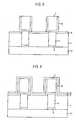
- FIGS. 1 to 8are cross-sectional views illustrating a method for fabricating a semiconductor device in accordance with the disclosure.
- an interlayer insulating layer 1is formed with an oxide layer on a substrate 11 undergone predetermined processes, and a SiON layer 2 , of which etch selectivity is higher than that of the oxide layer, is formed on the interlayer insulating layer 1 . Thereafter, the SiON layer 2 and the interlayer insulating layer 1 are selectively etched to form a contact hole exposing the substrate 11 . Next, a polysilicon plug (not shown) is formed in the contact hole for forming a vertical interconnection between the substrate 11 and a capacitor to be formed.
- a titanium layeris deposited to a thickness of about 100 ⁇ to about 300 ⁇ , and then a rapid thermal treatment (RTP) is carried out at a temperature of about 650° C. to about 800° C. to form a titanium silicide layer 3 for reducing contact resistance between the polysilicon plug and a barrier metal layer later to be formed on the polysilicon plug. Un-reacted titanium from the titanium layer is removed by a wet etch process.
- a titanium nitride layer 4is formed as the metal barrier layer on the substrate 11 , and the titanium nitride layer 4 is flattened, for example by a chemical mechanical polishing (CMP) process, to reach substantially the same height as the SiON layer 2 .
- CMPchemical mechanical polishing
- Various triatomic materialssuch as TiSiN, TiAlN, and TaSiN, can be used to form a metal barrier layer instead of titanium nitride.
- a sacrificial layer 5e.g., a silicon oxide layer, a phosphosilicate glass (PSG) layer, and the like
- a sacrificial layer 5for forming a lower electrode of a capacitor is deposited and selectively etched to expose the titanium nitride layer 4 .
- a photolithography, exposing, and etching processis used.
- a Pt seed layer 6is formed to a thickness of about 100 ⁇ to about 300 ⁇ , with a chemical vapor deposition (CVD) method, for example.
- CVDchemical vapor deposition
- a metal layer 7 for a lower electrode of a capacitoris formed, for example by depositing a metal such as Ru or Ir with a CVD method.
- portions of the metal layer 7 and the seed layer 6are removed, for example by CMP, until the surface of the sacrificial layer 5 is exposed.
- a Pt layer 8is formed on the entire surface of the substrate.
- a processsuch as a blanket etch-back process using a reactive ion etching method, is carried out to remove a portion of the pt layer 8 and leave the Pt layer 8 remaining on the upper surface of the metal layer 7 .
- a dielectric layer 9is formed, for example with an atomic layer deposition method or a metal organic chemical vapor deposition method.
- the dielectric layer 9preferably is formed of a high dielectric material, such as Ta 2 O 5 (“TaON”), STO, SBT, or BST; and in case of forming a ferroelectric random access memory, the dielectric layer 9 preferably is formed of a ferroelectric material, such as PZT, SBT, SBTN, or BLT.
- the dielectric layer 9is crystallized, for example by a rapid thermal nitridation (“RTN”) or a rapid thermal nitr-oxidation (“RTNO”) process at a temperature of about 650° C. to about 750° C. for about 10 seconds to about 180 seconds.
- RTNrapid thermal nitridation
- RTNOrapid thermal nitr-oxidation
- a top electrode 10is formed, for example with a CVD method, to a thickness of about 500 ⁇ to about 1000 ⁇ .
- the top electrode 10preferably is formed of a metal selected from the group consisting of Ru, Ir and Pt.
- a seed layer 6is formed; however the step of forming a seed layer can be omitted. That is, the lower electrode can be obtained by forming a metal pattern without a seed layer and by forming a Pt layer on an upper surface and sidewalls of the metal pattern.
Landscapes
- Semiconductor Memories (AREA)
Abstract
Description
- 1. Field of the Invention[0001]
- The invention relates to a semiconductor device and a method for forming a semiconductor device. More particularly, the invention relates to a capacitor for a semiconductor device and a method for forming the capacitor.[0002]
- 2. Brief Description of Related Technology[0003]
- Each of a dynamic random access memory (DRAM), which is the most widely used semiconductor memory device, and a ferroelectric random access memory (FeRAM), which has attracted much attention recently, has a unit cell structure consisting of one transistor and one capacitor. The unit cell structure of the DRAM and FeRAM is a superior structure from an integration respect.[0004]
- The capacitor of such semiconductor devices has a stacked structure including an upper electrode, a dielectric layer for charge storing, and a lower electrode. In a DRAM and a FeRAM, the capacitor is coupled to one active region of a transistor through a plug formed of doped polysilicon. The charge stored in the capacitor flow into a bit line through a channel of the transistor and another active region of the transistor.[0005]
- Methods for forming a highly integrated DRAM or FeRAM, employing high dielectric material or ferroelectric material for forming a capacitor dielectric layer, respectively, are described below. As used herein, the term “dielectric material” can include a ferroelectric material and “dielectric layer” can include a ferroelectric layer.[0006]
- An interlayer insulating layer and an etch barrier layer are formed on a semiconductor substrate on which a transistor and a bit line are formed. Thereafter, the interlayer insulating layer and the etch barrier layer are selectively etched to form a contact hole exposing an active region of the transistor, and a polysilicon plug is then formed in the contact hole to fill a portion of the contact hole.[0007]
- Subsequently, a titanium layer is deposited on the substrate and a rapid thermal process is performed to form a titanium silicide (TiSi[0008]x) layer by causing a reaction between silicon in the polysilicon plug and titanium in the titanium layer. The titanium layer remaining on the interlayer insulating layer is removed by a wet etching process. The TiSixlayer is an ohmic contact layer reducing contact resistance between the polysilicon plug and a diffusion barrier layer to be formed over the polysilicon plug.
- Next, a TiN layer is formed on the TiSi[0009]xlayer and the etch barrier layer. The TiN layer is then removed by a polishing process or an etching process until the surface of the etch barrier layer is exposed to leave the TiN layer only in the contact hole. The TiN layer plays the role of a diffusion barrier layer to prevent oxygen diffusing to the polysilicon plug or the substrate through a lower electrode of a capacitor during thermal treatment. Such a thermal treatment can be a part of a process for forming a high dielectric layer or a ferroelectric layer, for example.
- Thereafter, a lower electrode layer, a high dielectric layer (or a ferroelectric layer), and an upper electrode layer are deposited in order and pattern to form a capacitor. It is difficult to use polysilicon as an electrode material. Instead of polysilicon, noble metals, such as platinum (“Pt”), iridium (“Ir”), and ruthenium (“Ru”); conductive oxides, such as RuO[0010]2and IrO2; and conductive compounds such as TiN can be used to form the metal/insulator/metal(“MIM”) structure of a capacitor.
- A high dielectric layer made of SrTiO[0011]3(“STO”) or (Ba, Sr)TiO3(“BST”), and a ferroelectric layer made of Pb(Zr, Ti)O3(“PZT”), SrBi2Ta2O9(“SBT”), (SrxBi2-y)(Ta1-zNbz)2O9(“SBTN”), or (Bi, La)TiO3(“BLT”) are generally formed at very high temperature (e.g., from about 600° C. to about 1000° C.) in an oxygen atmosphere.
- When depositing a dielectric layer or performing a subsequent thermal treatment in an oxygen atmosphere, oxygen can diffuse into parts of the semiconductor device that are under the capacitor and cause problems such as formation of an isolation layer or a resistance material. For example, an isolation layer including SiO[0012]2can be formed on the surface of the polysilicon plug by diffused oxygen. Moreover, in the case of forming a lower electrode on a polysilicon plug using metal, such as Pt, a resistance material, such as PtSi, is easily formed by the reaction of the metal and silicon at a temperature above about 250° C., for example. Therefore, the problem of increased resistance is possible.
- To ameliorate the problem of resistance increase, a diffusion barrier layer is formed of TiN, as mentioned above. However, subsequent processing temperatures are limited to about 450° C. even if the barrier layer is formed of TiN, due to the potential for oxidizing TiN. Accordingly, a barrier material capable of effectively preventing the polysilicon being oxidized is desired. A triatomic barrier layer material, such as TiAlN, TiSiN, or TaSiN, is oxidized at a temperature as much as about 50° C. to about 100° C. higher than TiN. However, such a triatomic barrier layer is also easily oxidized at a temperature of over 550° C. That is, an insulating layer, such as a TiO[0013]2layer, an Al2O3layer, or a SiO2layer, is formed on the surface of the triatomic barrier layer because oxygen diffused through the lower electrode reacts with the Ti-based nitride layer or the polysilicon plug during a process for forming a capacitor.
- To secure the dielectric quality of a high dielectric layer, such as a layer made of STO or BST, and a ferroelectric layer, such as a layer made of PZT, SBT, SBTN, or BLT, the barrier layer preferably will resist or prevent oxidation of the polysilicon and resist or prevent oxidation of itself at a temperature over about 600° C.[0014]
- It is, therefore, desirable to provide a semiconductor device capable of resisting or preventing the diffusion of oxygen past a lower electrode during thermal processing, and a method for fabricating such a semiconductor device.[0015]
- Disclosed herein is a method of forming a capacitor, including the steps of: forming a lower electrode on a substrate, the lower electrode including a metal pattern and a layer including Pt covering an upper surface and sidewalls of the metal pattern, wherein the metal pattern is formed of a material having good antioxidant properties (e.g., capable of forming a conductive oxide); forming a dielectric layer on the lower electrode; and forming an upper electrode on the dielectric layer.[0016]
- Also disclosed herein is a capacitor, including: a lower electrode formed on a substrate, wherein the lower electrode includes a metal pattern and a layer including Pt covering an upper surface and sidewalls of the metal pattern, and wherein the metal pattern is formed of a material having good antioxidant properties (e.g., capable of forming a conductive oxide); a dielectric layer formed on the lower electrode; and an upper electrode formed on-the dielectric layer.[0017]
- A surface of the lower electrode can be formed of Pt having a work function that has a high difference with the work function of the dielectric material. An inner part of the lower electrode is formed of metal, for example a metal which forms a conductive oxide material, being a good antioxidant. The inner part of the lower electrode can be formed by depositing metal, such as Ru or Ir, by electro plating, for example.[0018]
- The above and other aspects of the disclosure will become apparent from the following description given in conjunction with the accompanying drawings, in which:[0019]
- FIGS.[0020]1 to8 are cross-sectional views illustrating a method for fabricating a semiconductor device in accordance with the disclosure.
- Referring to FIG. 1, an[0021]
interlayer insulating layer 1 is formed with an oxide layer on asubstrate 11 undergone predetermined processes, and aSiON layer 2, of which etch selectivity is higher than that of the oxide layer, is formed on theinterlayer insulating layer 1. Thereafter, theSiON layer 2 and theinterlayer insulating layer 1 are selectively etched to form a contact hole exposing thesubstrate 11. Next, a polysilicon plug (not shown) is formed in the contact hole for forming a vertical interconnection between thesubstrate 11 and a capacitor to be formed. - Subsequently, a titanium layer is deposited to a thickness of about 100 Å to about 300 Å, and then a rapid thermal treatment (RTP) is carried out at a temperature of about 650° C. to about 800° C. to form a[0022]
titanium silicide layer 3 for reducing contact resistance between the polysilicon plug and a barrier metal layer later to be formed on the polysilicon plug. Un-reacted titanium from the titanium layer is removed by a wet etch process. Next, atitanium nitride layer 4 is formed as the metal barrier layer on thesubstrate 11, and thetitanium nitride layer 4 is flattened, for example by a chemical mechanical polishing (CMP) process, to reach substantially the same height as theSiON layer 2. Various triatomic materials, such as TiSiN, TiAlN, and TaSiN, can be used to form a metal barrier layer instead of titanium nitride. - Thereafter, a sacrificial layer[0023]5 (e.g., a silicon oxide layer, a phosphosilicate glass (PSG) layer, and the like) for forming a lower electrode of a capacitor is deposited and selectively etched to expose the
titanium nitride layer 4. Preferably, a photolithography, exposing, and etching process is used. - Referring to FIG. 2, a[0024]
Pt seed layer 6 is formed to a thickness of about 100 Å to about 300 Å, with a chemical vapor deposition (CVD) method, for example. - Referring to FIG. 3, a[0025]
metal layer 7 for a lower electrode of a capacitor is formed, for example by depositing a metal such as Ru or Ir with a CVD method. - Referring to FIG. 4, portions of the[0026]
metal layer 7 and theseed layer 6 are removed, for example by CMP, until the surface of thesacrificial layer 5 is exposed. - Referring to FIG. 5, the[0027]
sacrificial layer 5 is removed. - Referring to FIG. 6, a[0028]
Pt layer 8 is formed on the entire surface of the substrate. - Referring to FIG. 7, a process, such as a blanket etch-back process using a reactive ion etching method, is carried out to remove a portion of the[0029]
pt layer 8 and leave thePt layer 8 remaining on the upper surface of themetal layer 7. - Referring to FIG. 8, a[0030]
dielectric layer 9 is formed, for example with an atomic layer deposition method or a metal organic chemical vapor deposition method. In the case of forming a dynamic random access memory, thedielectric layer 9 preferably is formed of a high dielectric material, such as Ta2O5(“TaON”), STO, SBT, or BST; and in case of forming a ferroelectric random access memory, thedielectric layer 9 preferably is formed of a ferroelectric material, such as PZT, SBT, SBTN, or BLT. Thereafter, thedielectric layer 9 is crystallized, for example by a rapid thermal nitridation (“RTN”) or a rapid thermal nitr-oxidation (“RTNO”) process at a temperature of about 650° C. to about 750° C. for about 10 seconds to about 180 seconds. - Subsequently, a[0031]
top electrode 10 is formed, for example with a CVD method, to a thickness of about 500 Å to about 1000 Å. Thetop electrode 10 preferably is formed of a metal selected from the group consisting of Ru, Ir and Pt. - In the above-described example, a[0032]
seed layer 6 is formed; however the step of forming a seed layer can be omitted. That is, the lower electrode can be obtained by forming a metal pattern without a seed layer and by forming a Pt layer on an upper surface and sidewalls of the metal pattern. - By forming the surface and the inner part of the lower electrode of the capacitor with Pt and a metal which forms a conductive metal oxide, respectively, it is possible to perform the thermal treatment for crystallizing a dielectric layer at a higher temperature, for example as much as about 150° C. to about 200° C., compared to the case of forming the lower electrode only with a TiN layer.[0033]
- Therefore, several advantages can be achieved by various examples of a process according to the disclosure. First, it is possible to reduce leakage current, for example by the use of a material such as Pt for forming the surface of the lower electrode. It is also possible to form a dielectric layer having a high dielectric constant, for example because it is possible to perform thermal treatment for crystallizing a dielectric layer at a temperature as much as 150° C. to about 200° C. higher than the case when a lower electrode is formed only with a TiN layer. Thus, the process burden due to the capacitor formation process can be minimized. Finally, it is also possible to perform a thermal treatment at a high temperature in an oxygen atmosphere, because the inner part of the lower electrode prevents oxygen from diffusing, so that a high dielectric layer can be obtained.[0034]
- Although the examples of the disclosure have been described for illustrative purposes, those skilled in the art will appreciate that various modifications, additions and substitutions are possible, without departing from the scope and spirit of the disclosure.[0035]
Claims (10)
1. A method for forming a capacitor, comprising the steps of:
forming a lower electrode including a metal pattern and a layer comprising Pt covering an upper surface and sidewalls of the metal pattern on a substrate, wherein the metal pattern is formed of a material capable of forming a conductive oxide;
forming a dielectric layer on the lower electrode; and
forming an upper electrode on the dielectric layer.
2. The method as recited inclaim 1 , wherein the step of forming the lower electrode includes the steps of:
forming a sacrificial layer on the substrate;
forming a contact hole by selectively etching the sacrificial layer;
forming a seed layer comprising Pt in the contact hole;
filling the contact hole with a metal layer for the metal pattern;
removing the sacrificial layer, whereby the metal pattern is exposed; and
forming the layer comprising Pt on the upper surface and sidewalls of the metal pattern.
3. The method as recited inclaim 2 , comprising forming the metal layer with an electro plating process.
4. The method as recited inclaim 2 , wherein the step of forming the layer comprising Pt includes the steps of:
forming the layer comprising Pt on the metal pattern with a sputtering method; and
performing a blanket etch back process with a reactive ion etching process, whereby the layer comprising Pt remains on the upper surface and sidewalls of the metal pattern.
5. The method as recited inclaim 2 , comprising forming the seed layer to a thickness of about 100 Å to about 300 Å.
6. The method as recited inclaim 2 , comprising forming the seed layer with a chemical vapor deposition method.
7. The method as recited inclaim 2 , comprising forming the metal pattern comprising a metal selected from the group consisting of Ru and Ir.
8. A capacitor comprising:
a lower electrode formed on a substrate, wherein the lower electrode includes a metal pattern and a layer comprising Pt covering an upper surface and sidewalls of the metal pattern, and wherein the metal pattern is formed of a material capable of forming a conductive oxide;
a dielectric layer formed on the lower electrode; and
an upper electrode formed on the dielectric layer.
9. The capacitor as recited inclaim 8 , further comprising a seed layer comprising Pt between the substrate and the metal pattern.
10. The capacitor as recited inclaim 9 , wherein the metal pattern is formed comprising a metal selected from the group consisting of Ru and Ir.
Priority Applications (1)
| Application Number | Priority Date | Filing Date | Title |
|---|---|---|---|
| US10/759,457US7042034B2 (en) | 2001-09-12 | 2004-01-16 | Capacitor |
Applications Claiming Priority (4)
| Application Number | Priority Date | Filing Date | Title |
|---|---|---|---|
| KR10-2001-0056136AKR100422594B1 (en) | 2001-09-12 | 2001-09-12 | Capacitor in semiconductor device and method for fabricating the same |
| KR2001-56136 | 2001-09-12 | ||
| US10/236,311US6689623B2 (en) | 2001-09-12 | 2002-09-06 | Method for forming a capacitor |
| US10/759,457US7042034B2 (en) | 2001-09-12 | 2004-01-16 | Capacitor |
Related Parent Applications (1)
| Application Number | Title | Priority Date | Filing Date |
|---|---|---|---|
| US10/236,311DivisionUS6689623B2 (en) | 2001-09-12 | 2002-09-06 | Method for forming a capacitor |
Publications (2)
| Publication Number | Publication Date |
|---|---|
| US20040147088A1true US20040147088A1 (en) | 2004-07-29 |
| US7042034B2 US7042034B2 (en) | 2006-05-09 |
Family
ID=19714195
Family Applications (2)
| Application Number | Title | Priority Date | Filing Date |
|---|---|---|---|
| US10/236,311Expired - Fee RelatedUS6689623B2 (en) | 2001-09-12 | 2002-09-06 | Method for forming a capacitor |
| US10/759,457Expired - Fee RelatedUS7042034B2 (en) | 2001-09-12 | 2004-01-16 | Capacitor |
Family Applications Before (1)
| Application Number | Title | Priority Date | Filing Date |
|---|---|---|---|
| US10/236,311Expired - Fee RelatedUS6689623B2 (en) | 2001-09-12 | 2002-09-06 | Method for forming a capacitor |
Country Status (2)
| Country | Link |
|---|---|
| US (2) | US6689623B2 (en) |
| KR (1) | KR100422594B1 (en) |
Cited By (3)
| Publication number | Priority date | Publication date | Assignee | Title |
|---|---|---|---|---|
| US20090072349A1 (en)* | 2007-09-13 | 2009-03-19 | Samsung Electronics, Co., Ltd. | Semiconductor device and method of manufacturing the same |
| US7582549B2 (en) | 2006-08-25 | 2009-09-01 | Micron Technology, Inc. | Atomic layer deposited barium strontium titanium oxide films |
| US12150295B2 (en) | 2021-01-04 | 2024-11-19 | Changxin Memory Technologies, Inc. | Method for manufacturing a memory using a plurality of sacrificial pillars |
Families Citing this family (4)
| Publication number | Priority date | Publication date | Assignee | Title |
|---|---|---|---|---|
| KR100583090B1 (en)* | 2003-05-30 | 2006-05-23 | 주식회사 하이닉스반도체 | Capacitor Manufacturing Method of Ferroelectric Resistors |
| KR100780610B1 (en)* | 2003-11-28 | 2007-11-29 | 주식회사 하이닉스반도체 | Semiconductor device manufacturing method |
| KR100675895B1 (en)* | 2005-06-29 | 2007-02-02 | 주식회사 하이닉스반도체 | Metal wiring structure of semiconductor device and manufacturing method |
| CN114725018B (en)* | 2021-01-04 | 2024-06-21 | 长鑫存储技术有限公司 | Memory and preparation method thereof |
Citations (27)
| Publication number | Priority date | Publication date | Assignee | Title |
|---|---|---|---|---|
| US5566045A (en)* | 1994-08-01 | 1996-10-15 | Texas Instruments, Inc. | High-dielectric-constant material electrodes comprising thin platinum layers |
| US5877062A (en)* | 1996-11-13 | 1999-03-02 | Samsung Electronics Co., Ltd. | Methods of forming integrated circuit capacitors having protected diffusion barrier metal layers therein |
| US5879957A (en)* | 1996-12-03 | 1999-03-09 | Lg Semicon Co., Ltd. | Method for manufacturing a capacitor |
| US6011284A (en)* | 1996-12-26 | 2000-01-04 | Sony Corporation | Electronic material, its manufacturing method, dielectric capacitor, nonvolatile memory and semiconductor device |
| US6096391A (en)* | 1998-10-16 | 2000-08-01 | Wilson Greatbatch Ltd. | Method for improving electrical conductivity of metals, metal alloys and metal oxides |
| US6107136A (en)* | 1998-08-17 | 2000-08-22 | Motorola Inc. | Method for forming a capacitor structure |
| US6110529A (en)* | 1990-07-06 | 2000-08-29 | Advanced Tech Materials | Method of forming metal films on a substrate by chemical vapor deposition |
| US6127277A (en)* | 1996-07-03 | 2000-10-03 | Tegal Corporation | Method and apparatus for etching a semiconductor wafer with features having vertical sidewalls |
| US6144060A (en)* | 1997-07-31 | 2000-11-07 | Samsung Electronics Co., Ltd. | Integrated circuit devices having buffer layers therein which contain metal oxide stabilized by heat treatment under low temperature |
| US6165623A (en)* | 1996-11-07 | 2000-12-26 | Cabot Corporation | Niobium powders and niobium electrolytic capacitors |
| US6190496B1 (en)* | 1996-07-03 | 2001-02-20 | Tegal Corporation | Plasma etch reactor and method for emerging films |
| US6255167B1 (en)* | 1998-06-03 | 2001-07-03 | Texas Instruments - Acer Incorporated | Method of forming high density buried bit line flash EEPROM memory cell with a shallow trench floating gate |
| US20010055851A1 (en)* | 2000-06-13 | 2001-12-27 | Samsung Electronics Co., Ltd. | Method for forming capacitor of semiconductor memory device using electrolplating method |
| US20020016036A1 (en)* | 2000-06-28 | 2002-02-07 | Kwon Hong | Method for fabricating a capacitor in a semiconductor device |
| US6358810B1 (en)* | 1998-07-28 | 2002-03-19 | Applied Materials, Inc. | Method for superior step coverage and interface control for high K dielectric capacitors and related electrodes |
| US6384443B1 (en)* | 1999-11-18 | 2002-05-07 | Mitsubishi Denki Kabushiki Kaisha | Stacked capacitor and method of manufacturing same |
| US6395601B2 (en)* | 1999-12-29 | 2002-05-28 | Hyundai Electronics Industries Co., Ltd. | Method for forming a lower electrode for use in a semiconductor device |
| US20020074661A1 (en)* | 2000-12-20 | 2002-06-20 | Mitsubishi Denki Kabushiki Kaisha | Semiconductor device and method of manufacturing the same |
| US6451666B2 (en)* | 1999-12-27 | 2002-09-17 | Hyundai Electronics Industries Co., Ltd | Method for forming a lower electrode by using an electroplating method |
| US6468858B1 (en)* | 2001-03-23 | 2002-10-22 | Taiwan Semiconductor Manufacturing Company | Method of forming a metal insulator metal capacitor structure |
| US20020179566A1 (en)* | 2001-05-03 | 2002-12-05 | Jong-Bum Park | Method for manufacturing a capacitor |
| US6511912B1 (en)* | 2000-08-22 | 2003-01-28 | Micron Technology, Inc. | Method of forming a non-conformal layer over and exposing a trench |
| US6521494B2 (en)* | 2000-01-26 | 2003-02-18 | Hitachi, Ltd. | Method of manufacturing semiconductor devices utilizing underlayer-dependency of deposition of capacitor electrode film, and semiconductor device |
| US20030042609A1 (en)* | 2001-08-29 | 2003-03-06 | Hyung-Bok Choi | Semiconductor device and method of fabricating the same |
| US20040041194A1 (en)* | 2002-08-29 | 2004-03-04 | Micron Technology, Inc. | Metal plating using seed film |
| US20040135182A1 (en)* | 2002-11-11 | 2004-07-15 | Hyeong-Geun An | Ferroelectric capacitors including a seed conductive film and methods for manufacturing the same |
| US20050032346A1 (en)* | 2003-08-05 | 2005-02-10 | Graettinger Thomas M. | Stud electrode and process for making same |
Family Cites Families (12)
| Publication number | Priority date | Publication date | Assignee | Title |
|---|---|---|---|---|
| KR19980014897A (en)* | 1996-08-17 | 1998-05-25 | 구자홍 | Capacitor and method of manufacturing the same |
| KR100273228B1 (en)* | 1997-09-27 | 2001-01-15 | 김영환 | Manufacturing method for capacitor |
| KR100318453B1 (en)* | 1998-06-29 | 2002-03-08 | 박종섭 | METHOD FOR FORMING CAPACITOR HAVING BOTTOM ELECTRODE FORMED BY Ir/Pt DOUBLE LAYER |
| WO2000039842A1 (en)* | 1998-12-23 | 2000-07-06 | Infineon Technologies Ag | Capacitor electrode structure |
| JP2001237395A (en)* | 2000-02-22 | 2001-08-31 | Matsushita Electric Ind Co Ltd | Semiconductor storage device |
| KR100593137B1 (en)* | 2000-06-19 | 2006-06-26 | 주식회사 하이닉스반도체 | Storage electrode formation method of high dielectric capacitor |
| KR100646947B1 (en)* | 2000-06-29 | 2006-11-17 | 주식회사 하이닉스반도체 | Capacitor manufacturing method of semiconductor device |
| KR20020002633A (en)* | 2000-06-30 | 2002-01-10 | 박종섭 | A method for forming a storage node of a semiconductor device |
| KR100501595B1 (en)* | 2000-11-15 | 2005-07-14 | 주식회사 하이닉스반도체 | Method of manufacturing a capacitor in a semiconductor device |
| KR100504943B1 (en)* | 2000-11-15 | 2005-08-03 | 주식회사 하이닉스반도체 | Method of manufacturing a capacitor in a semiconductor device |
| KR20020045261A (en)* | 2000-12-08 | 2002-06-19 | 박종섭 | Method of manufacturing a capacitor |
| KR100418585B1 (en)* | 2001-06-30 | 2004-02-14 | 주식회사 하이닉스반도체 | Method for fabrication of ferroelectric random access memory |
- 2001
- 2001-09-12KRKR10-2001-0056136Apatent/KR100422594B1/ennot_activeExpired - Fee Related
- 2002
- 2002-09-06USUS10/236,311patent/US6689623B2/ennot_activeExpired - Fee Related
- 2004
- 2004-01-16USUS10/759,457patent/US7042034B2/ennot_activeExpired - Fee Related
Patent Citations (31)
| Publication number | Priority date | Publication date | Assignee | Title |
|---|---|---|---|---|
| US6110529A (en)* | 1990-07-06 | 2000-08-29 | Advanced Tech Materials | Method of forming metal films on a substrate by chemical vapor deposition |
| US5619393A (en)* | 1994-08-01 | 1997-04-08 | Texas Instruments Incorporated | High-dielectric-constant material electrodes comprising thin ruthenium dioxide layers |
| US5566045A (en)* | 1994-08-01 | 1996-10-15 | Texas Instruments, Inc. | High-dielectric-constant material electrodes comprising thin platinum layers |
| US6190496B1 (en)* | 1996-07-03 | 2001-02-20 | Tegal Corporation | Plasma etch reactor and method for emerging films |
| US6127277A (en)* | 1996-07-03 | 2000-10-03 | Tegal Corporation | Method and apparatus for etching a semiconductor wafer with features having vertical sidewalls |
| US6165623A (en)* | 1996-11-07 | 2000-12-26 | Cabot Corporation | Niobium powders and niobium electrolytic capacitors |
| US5877062A (en)* | 1996-11-13 | 1999-03-02 | Samsung Electronics Co., Ltd. | Methods of forming integrated circuit capacitors having protected diffusion barrier metal layers therein |
| US5879957A (en)* | 1996-12-03 | 1999-03-09 | Lg Semicon Co., Ltd. | Method for manufacturing a capacitor |
| US6011284A (en)* | 1996-12-26 | 2000-01-04 | Sony Corporation | Electronic material, its manufacturing method, dielectric capacitor, nonvolatile memory and semiconductor device |
| US6144060A (en)* | 1997-07-31 | 2000-11-07 | Samsung Electronics Co., Ltd. | Integrated circuit devices having buffer layers therein which contain metal oxide stabilized by heat treatment under low temperature |
| US6255167B1 (en)* | 1998-06-03 | 2001-07-03 | Texas Instruments - Acer Incorporated | Method of forming high density buried bit line flash EEPROM memory cell with a shallow trench floating gate |
| US6358810B1 (en)* | 1998-07-28 | 2002-03-19 | Applied Materials, Inc. | Method for superior step coverage and interface control for high K dielectric capacitors and related electrodes |
| US6107136A (en)* | 1998-08-17 | 2000-08-22 | Motorola Inc. | Method for forming a capacitor structure |
| US6096391A (en)* | 1998-10-16 | 2000-08-01 | Wilson Greatbatch Ltd. | Method for improving electrical conductivity of metals, metal alloys and metal oxides |
| US6384443B1 (en)* | 1999-11-18 | 2002-05-07 | Mitsubishi Denki Kabushiki Kaisha | Stacked capacitor and method of manufacturing same |
| US6451666B2 (en)* | 1999-12-27 | 2002-09-17 | Hyundai Electronics Industries Co., Ltd | Method for forming a lower electrode by using an electroplating method |
| US6395601B2 (en)* | 1999-12-29 | 2002-05-28 | Hyundai Electronics Industries Co., Ltd. | Method for forming a lower electrode for use in a semiconductor device |
| US6521494B2 (en)* | 2000-01-26 | 2003-02-18 | Hitachi, Ltd. | Method of manufacturing semiconductor devices utilizing underlayer-dependency of deposition of capacitor electrode film, and semiconductor device |
| US20010055851A1 (en)* | 2000-06-13 | 2001-12-27 | Samsung Electronics Co., Ltd. | Method for forming capacitor of semiconductor memory device using electrolplating method |
| US6630387B2 (en)* | 2000-06-13 | 2003-10-07 | Samsung Electronics Co., Ltd. | Method for forming capacitor of semiconductor memory device using electroplating method |
| US20020016036A1 (en)* | 2000-06-28 | 2002-02-07 | Kwon Hong | Method for fabricating a capacitor in a semiconductor device |
| US6511912B1 (en)* | 2000-08-22 | 2003-01-28 | Micron Technology, Inc. | Method of forming a non-conformal layer over and exposing a trench |
| US20030096498A1 (en)* | 2000-08-22 | 2003-05-22 | Dinesh Chopra | Method of providing a structure using self-aligned features |
| US20040219738A1 (en)* | 2000-08-22 | 2004-11-04 | Dinesh Chopra | Method of providing a structure using self-aligned features |
| US20020074661A1 (en)* | 2000-12-20 | 2002-06-20 | Mitsubishi Denki Kabushiki Kaisha | Semiconductor device and method of manufacturing the same |
| US6468858B1 (en)* | 2001-03-23 | 2002-10-22 | Taiwan Semiconductor Manufacturing Company | Method of forming a metal insulator metal capacitor structure |
| US20020179566A1 (en)* | 2001-05-03 | 2002-12-05 | Jong-Bum Park | Method for manufacturing a capacitor |
| US20030042609A1 (en)* | 2001-08-29 | 2003-03-06 | Hyung-Bok Choi | Semiconductor device and method of fabricating the same |
| US20040041194A1 (en)* | 2002-08-29 | 2004-03-04 | Micron Technology, Inc. | Metal plating using seed film |
| US20040135182A1 (en)* | 2002-11-11 | 2004-07-15 | Hyeong-Geun An | Ferroelectric capacitors including a seed conductive film and methods for manufacturing the same |
| US20050032346A1 (en)* | 2003-08-05 | 2005-02-10 | Graettinger Thomas M. | Stud electrode and process for making same |
Cited By (5)
| Publication number | Priority date | Publication date | Assignee | Title |
|---|---|---|---|---|
| US7582549B2 (en) | 2006-08-25 | 2009-09-01 | Micron Technology, Inc. | Atomic layer deposited barium strontium titanium oxide films |
| US8581352B2 (en) | 2006-08-25 | 2013-11-12 | Micron Technology, Inc. | Electronic devices including barium strontium titanium oxide films |
| US9202686B2 (en) | 2006-08-25 | 2015-12-01 | Micron Technology, Inc. | Electronic devices including barium strontium titanium oxide films |
| US20090072349A1 (en)* | 2007-09-13 | 2009-03-19 | Samsung Electronics, Co., Ltd. | Semiconductor device and method of manufacturing the same |
| US12150295B2 (en) | 2021-01-04 | 2024-11-19 | Changxin Memory Technologies, Inc. | Method for manufacturing a memory using a plurality of sacrificial pillars |
Also Published As
| Publication number | Publication date |
|---|---|
| US6689623B2 (en) | 2004-02-10 |
| US7042034B2 (en) | 2006-05-09 |
| KR100422594B1 (en) | 2004-03-16 |
| US20030048593A1 (en) | 2003-03-13 |
| KR20030023141A (en) | 2003-03-19 |
Similar Documents
| Publication | Publication Date | Title |
|---|---|---|
| JP5047250B2 (en) | Manufacturing method of semiconductor device | |
| US20040180453A1 (en) | Ferroelectric memory device and method of forming the same | |
| US7205192B2 (en) | Semiconductor memory device capable of preventing oxidation of plug and method for fabricating the same | |
| US6184074B1 (en) | Method of fabrication a self-aligned polysilicon/diffusion barrier/oxygen stable sidewall bottom electrode structure for high-K DRAMS | |
| KR100815657B1 (en) | Capacitor, method for fabricating the capacitor, and method for fabricating semiconductor device | |
| US6682974B2 (en) | Fabricating capacitor of semiconductor device | |
| US20030059959A1 (en) | Method for fabricating capacitor | |
| US6689623B2 (en) | Method for forming a capacitor | |
| KR100219506B1 (en) | Capacitor Manufacturing Method of Semiconductor Device | |
| KR100402943B1 (en) | High dielectric capacitor and a method of manufacturing the same | |
| US20010018237A1 (en) | Method for fabricating a nonvolatile dram memory cell | |
| KR100633330B1 (en) | Capacitor Manufacturing Method of Semiconductor Device | |
| JP2002373975A (en) | Method of manufacturing ferroelectric memory device and ferroelectric memory device | |
| US6306666B1 (en) | Method for fabricating ferroelectric memory device | |
| KR100614576B1 (en) | Capacitor Manufacturing Method | |
| KR100604659B1 (en) | Capacitor Formation Method of Semiconductor Device | |
| JP3929743B2 (en) | Capacitor element manufacturing method | |
| JP4632620B2 (en) | Manufacturing method of semiconductor device | |
| KR100687433B1 (en) | Method of forming lower electrode of capacitor | |
| KR100688054B1 (en) | Fabrication of Conductor Capacitor of Ferroelectric Device | |
| KR20010059002A (en) | A method for forming capacitor in semiconductor device | |
| KR100448242B1 (en) | Method for fabricating capacitor top electrode in semiconductor device | |
| KR100418585B1 (en) | Method for fabrication of ferroelectric random access memory | |
| KR20010027679A (en) | Capacitor of a semiconductor device having low contact resistance between a lower electrode and a contact plug and method for fabricating the same | |
| KR20020094176A (en) | Method of forming memory device having electroplating electrode |
Legal Events
| Date | Code | Title | Description |
|---|---|---|---|
| FEPP | Fee payment procedure | Free format text:PAYOR NUMBER ASSIGNED (ORIGINAL EVENT CODE: ASPN); ENTITY STATUS OF PATENT OWNER: LARGE ENTITY | |
| FPAY | Fee payment | Year of fee payment:4 | |
| FEPP | Fee payment procedure | Free format text:PAYOR NUMBER ASSIGNED (ORIGINAL EVENT CODE: ASPN); ENTITY STATUS OF PATENT OWNER: LARGE ENTITY Free format text:PAYER NUMBER DE-ASSIGNED (ORIGINAL EVENT CODE: RMPN); ENTITY STATUS OF PATENT OWNER: LARGE ENTITY | |
| FPAY | Fee payment | Year of fee payment:8 | |
| FEPP | Fee payment procedure | Free format text:MAINTENANCE FEE REMINDER MAILED (ORIGINAL EVENT CODE: REM.) | |
| LAPS | Lapse for failure to pay maintenance fees | Free format text:PATENT EXPIRED FOR FAILURE TO PAY MAINTENANCE FEES (ORIGINAL EVENT CODE: EXP.) | |
| STCH | Information on status: patent discontinuation | Free format text:PATENT EXPIRED DUE TO NONPAYMENT OF MAINTENANCE FEES UNDER 37 CFR 1.362 | |
| FP | Lapsed due to failure to pay maintenance fee | Effective date:20180509 |