US20040146560A1 - Oriented nanostructures and methods of preparing - Google Patents
Oriented nanostructures and methods of preparingDownload PDFInfo
- Publication number
- US20040146560A1 US20040146560A1US10/656,911US65691103AUS2004146560A1US 20040146560 A1US20040146560 A1US 20040146560A1US 65691103 AUS65691103 AUS 65691103AUS 2004146560 A1US2004146560 A1US 2004146560A1
- Authority
- US
- United States
- Prior art keywords
- nanostructures
- composition
- matrix
- alignment
- nanostructure
- Prior art date
- Legal status (The legal status is an assumption and is not a legal conclusion. Google has not performed a legal analysis and makes no representation as to the accuracy of the status listed.)
- Granted
Links
- 239000002086nanomaterialSubstances0.000titleclaimsabstractdescription479
- 238000000034methodMethods0.000titleclaimsabstractdescription105
- 239000000203mixtureSubstances0.000claimsabstractdescription139
- 239000003446ligandSubstances0.000claimsdescription189
- 239000011159matrix materialSubstances0.000claimsdescription141
- 239000002070nanowireSubstances0.000claimsdescription73
- 239000002159nanocrystalSubstances0.000claimsdescription40
- 239000000758substrateSubstances0.000claimsdescription32
- 230000000295complement effectEffects0.000claimsdescription31
- 230000003993interactionEffects0.000claimsdescription28
- -1nanodotsSubstances0.000claimsdescription28
- 239000002073nanorodSubstances0.000claimsdescription24
- 150000001412aminesChemical class0.000claimsdescription17
- 238000004132cross linkingMethods0.000claimsdescription17
- RAXXELZNTBOGNW-UHFFFAOYSA-NimidazoleNatural productsC1=CNC=N1RAXXELZNTBOGNW-UHFFFAOYSA-N0.000claimsdescription15
- YBJHBAHKTGYVGT-ZKWXMUAHSA-N(+)-BiotinChemical compoundN1C(=O)N[C@@H]2[C@H](CCCCC(=O)O)SC[C@@H]21YBJHBAHKTGYVGT-ZKWXMUAHSA-N0.000claimsdescription14
- 238000001816coolingMethods0.000claimsdescription14
- 238000010438heat treatmentMethods0.000claimsdescription14
- 239000013522chelantSubstances0.000claimsdescription13
- XYFCBTPGUUZFHI-UHFFFAOYSA-NPhosphineChemical compoundPXYFCBTPGUUZFHI-UHFFFAOYSA-N0.000claimsdescription12
- YCIMNLLNPGFGHC-UHFFFAOYSA-NcatecholChemical compoundOC1=CC=CC=C1OYCIMNLLNPGFGHC-UHFFFAOYSA-N0.000claimsdescription12
- 150000001875compoundsChemical class0.000claimsdescription12
- JUJWROOIHBZHMG-UHFFFAOYSA-NPyridineChemical compoundC1=CC=NC=C1JUJWROOIHBZHMG-UHFFFAOYSA-N0.000claimsdescription10
- 230000008878couplingEffects0.000claimsdescription10
- 238000010168coupling processMethods0.000claimsdescription10
- 238000005859coupling reactionMethods0.000claimsdescription10
- 229910052739hydrogenInorganic materials0.000claimsdescription10
- 239000001257hydrogenSubstances0.000claimsdescription10
- 239000000412dendrimerSubstances0.000claimsdescription8
- 229920000736dendritic polymerPolymers0.000claimsdescription8
- 238000000151depositionMethods0.000claimsdescription8
- 239000002077nanosphereSubstances0.000claimsdescription8
- 229960002685biotinDrugs0.000claimsdescription7
- 235000020958biotinNutrition0.000claimsdescription7
- 239000011616biotinSubstances0.000claimsdescription7
- 150000003573thiolsChemical group0.000claimsdescription7
- HZAXFHJVJLSVMW-UHFFFAOYSA-N2-Aminoethan-1-olChemical compoundNCCOHZAXFHJVJLSVMW-UHFFFAOYSA-N0.000claimsdescription6
- VEUMANXWQDHAJV-UHFFFAOYSA-N2-[2-[(2-hydroxyphenyl)methylideneamino]ethyliminomethyl]phenolChemical compoundOC1=CC=CC=C1C=NCCN=CC1=CC=CC=C1OVEUMANXWQDHAJV-UHFFFAOYSA-N0.000claimsdescription6
- 108091023037AptamerProteins0.000claimsdescription6
- 108090001008AvidinProteins0.000claimsdescription6
- KXDHJXZQYSOELW-UHFFFAOYSA-MCarbamateChemical compoundNC([O-])=OKXDHJXZQYSOELW-UHFFFAOYSA-M0.000claimsdescription6
- ABLZXFCXXLZCGV-UHFFFAOYSA-NPhosphorous acidChemical compoundOP(O)=OABLZXFCXXLZCGV-UHFFFAOYSA-N0.000claimsdescription6
- XSQUKJJJFZCRTK-UHFFFAOYSA-NUreaChemical compoundNC(N)=OXSQUKJJJFZCRTK-UHFFFAOYSA-N0.000claimsdescription6
- 150000001408amidesChemical class0.000claimsdescription6
- 239000004202carbamideSubstances0.000claimsdescription6
- 239000012948isocyanateSubstances0.000claimsdescription6
- 150000002513isocyanatesChemical class0.000claimsdescription6
- 229910000073phosphorus hydrideInorganic materials0.000claimsdescription6
- MDDUHVRJJAFRAU-YZNNVMRBSA-Ntert-butyl-[(1r,3s,5z)-3-[tert-butyl(dimethyl)silyl]oxy-5-(2-diphenylphosphorylethylidene)-4-methylidenecyclohexyl]oxy-dimethylsilaneChemical compoundC1[C@@H](O[Si](C)(C)C(C)(C)C)C[C@H](O[Si](C)(C)C(C)(C)C)C(=C)\C1=C/CP(=O)(C=1C=CC=CC=1)C1=CC=CC=C1MDDUHVRJJAFRAU-YZNNVMRBSA-N0.000claimsdescription6
- 239000012808vapor phaseSubstances0.000claimsdescription6
- UQOKRDJILZMZKU-UHFFFAOYSA-N2-nitropyrimidineChemical compound[O-][N+](=O)C1=NC=CC=N1UQOKRDJILZMZKU-UHFFFAOYSA-N0.000claimsdescription5
- LFQSCWFLJHTTHZ-UHFFFAOYSA-NEthanolChemical compoundCCOLFQSCWFLJHTTHZ-UHFFFAOYSA-N0.000claimsdescription5
- UMJSCPRVCHMLSP-UHFFFAOYSA-NpyridineNatural productsCOC1=CC=CN=C1UMJSCPRVCHMLSP-UHFFFAOYSA-N0.000claimsdescription5
- 230000008021depositionEffects0.000claimsdescription4
- 108090001090LectinsProteins0.000claimsdescription3
- 102000004856LectinsHuman genes0.000claimsdescription3
- 238000005411Van der Waals forceMethods0.000claimsdescription3
- LEOOSTWEONVEMC-UHFFFAOYSA-Naniline;phosphenous acidChemical compoundOP=O.NC1=CC=CC=C1LEOOSTWEONVEMC-UHFFFAOYSA-N0.000claimsdescription3
- 239000000427antigenSubstances0.000claimsdescription3
- 108091007433antigensProteins0.000claimsdescription3
- 102000036639antigensHuman genes0.000claimsdescription3
- 150000001720carbohydratesChemical class0.000claimsdescription3
- 229940031098ethanolamineDrugs0.000claimsdescription3
- 239000002523lectinSubstances0.000claimsdescription3
- 108020004707nucleic acidsProteins0.000claimsdescription3
- 150000007523nucleic acidsChemical class0.000claimsdescription3
- 102000039446nucleic acidsHuman genes0.000claimsdescription3
- 108090000623proteins and genesProteins0.000claimsdescription3
- 102000004169proteins and genesHuman genes0.000claimsdescription3
- 238000007740vapor depositionMethods0.000claimsdescription3
- 230000009881electrostatic interactionEffects0.000claimsdescription2
- 239000012071phaseSubstances0.000claimsdescription2
- 230000000379polymerizing effectEffects0.000claimsdescription2
- 150000001735carboxylic acidsChemical class0.000claims2
- 239000000463materialSubstances0.000description35
- 230000015572biosynthetic processEffects0.000description24
- 239000004065semiconductorSubstances0.000description24
- 239000010410layerSubstances0.000description22
- 239000000126substanceSubstances0.000description20
- 238000003786synthesis reactionMethods0.000description19
- 239000000470constituentSubstances0.000description10
- 239000002019doping agentSubstances0.000description9
- 229920000642polymerPolymers0.000description8
- 238000002360preparation methodMethods0.000description8
- 230000008569processEffects0.000description8
- 239000013598vectorSubstances0.000description8
- 239000013078crystalSubstances0.000description7
- 239000000178monomerSubstances0.000description7
- 239000002105nanoparticleSubstances0.000description7
- 229910052710siliconInorganic materials0.000description7
- 238000013459approachMethods0.000description6
- 238000003491arrayMethods0.000description6
- UHYPYGJEEGLRJD-UHFFFAOYSA-Ncadmium(2+);selenium(2-)Chemical compound[Se-2].[Cd+2]UHYPYGJEEGLRJD-UHFFFAOYSA-N0.000description6
- 238000004519manufacturing processMethods0.000description6
- 239000002094self assembled monolayerSubstances0.000description6
- 239000004054semiconductor nanocrystalSubstances0.000description6
- OKTJSMMVPCPJKN-UHFFFAOYSA-NCarbonChemical compound[C]OKTJSMMVPCPJKN-UHFFFAOYSA-N0.000description5
- 239000002041carbon nanotubeSubstances0.000description5
- 150000001732carboxylic acid derivativesChemical class0.000description5
- 239000002071nanotubeSubstances0.000description5
- 239000002096quantum dotSubstances0.000description5
- 241000894007speciesSpecies0.000description5
- 239000011800void materialSubstances0.000description5
- 239000004971Cross linkerSubstances0.000description4
- 229910000673Indium arsenideInorganic materials0.000description4
- 229910045601alloyInorganic materials0.000description4
- 239000000956alloySubstances0.000description4
- 229910021393carbon nanotubeInorganic materials0.000description4
- RPQDHPTXJYYUPQ-UHFFFAOYSA-Nindium arsenideChemical compound[In]#[As]RPQDHPTXJYYUPQ-UHFFFAOYSA-N0.000description4
- 229910044991metal oxideInorganic materials0.000description4
- 150000004706metal oxidesChemical class0.000description4
- 239000002074nanoribbonSubstances0.000description4
- 230000003287optical effectEffects0.000description4
- 239000002245particleSubstances0.000description4
- 230000000737periodic effectEffects0.000description4
- 125000006239protecting groupChemical group0.000description4
- 239000000523sampleSubstances0.000description4
- 229910052711seleniumInorganic materials0.000description4
- 239000013545self-assembled monolayerSubstances0.000description4
- 239000002904solventSubstances0.000description4
- 229910052714telluriumInorganic materials0.000description4
- 229920000106Liquid crystal polymerPolymers0.000description3
- 239000004977Liquid-crystal polymers (LCPs)Substances0.000description3
- XUIMIQQOPSSXEZ-UHFFFAOYSA-NSiliconChemical compound[Si]XUIMIQQOPSSXEZ-UHFFFAOYSA-N0.000description3
- YXFVVABEGXRONW-UHFFFAOYSA-NTolueneChemical compoundCC1=CC=CC=C1YXFVVABEGXRONW-UHFFFAOYSA-N0.000description3
- 229910052782aluminiumInorganic materials0.000description3
- 229920001940conductive polymerPolymers0.000description3
- 239000004020conductorSubstances0.000description3
- 239000011258core-shell materialSubstances0.000description3
- 230000007547defectEffects0.000description3
- 230000005669field effectEffects0.000description3
- 229910052738indiumInorganic materials0.000description3
- 238000000608laser ablationMethods0.000description3
- 229910052751metalInorganic materials0.000description3
- 239000002184metalSubstances0.000description3
- 238000002156mixingMethods0.000description3
- 230000004001molecular interactionEffects0.000description3
- QJGQUHMNIGDVPM-UHFFFAOYSA-Nnitrogen groupChemical group[N]QJGQUHMNIGDVPM-UHFFFAOYSA-N0.000description3
- 239000010703siliconSubstances0.000description3
- 239000007787solidSubstances0.000description3
- 238000006467substitution reactionMethods0.000description3
- 229910052717sulfurInorganic materials0.000description3
- YBNMDCCMCLUHBL-UHFFFAOYSA-N(2,5-dioxopyrrolidin-1-yl) 4-pyren-1-ylbutanoateChemical compoundC=1C=C(C2=C34)C=CC3=CC=CC4=CC=C2C=1CCCC(=O)ON1C(=O)CCC1=OYBNMDCCMCLUHBL-UHFFFAOYSA-N0.000description2
- CDAWCLOXVUBKRW-UHFFFAOYSA-N2-aminophenolChemical compoundNC1=CC=CC=C1OCDAWCLOXVUBKRW-UHFFFAOYSA-N0.000description2
- CUYKNJBYIJFRCU-UHFFFAOYSA-N3-aminopyridineChemical compoundNC1=CC=CN=C1CUYKNJBYIJFRCU-UHFFFAOYSA-N0.000description2
- 229910017115AlSbInorganic materials0.000description2
- XMWRBQBLMFGWIX-UHFFFAOYSA-NC60 fullereneChemical compoundC12=C3C(C4=C56)=C7C8=C5C5=C9C%10=C6C6=C4C1=C1C4=C6C6=C%10C%10=C9C9=C%11C5=C8C5=C8C7=C3C3=C7C2=C1C1=C2C4=C6C4=C%10C6=C9C9=C%11C5=C5C8=C3C3=C7C1=C1C2=C4C6=C2C9=C5C3=C12XMWRBQBLMFGWIX-UHFFFAOYSA-N0.000description2
- 229910004613CdTeInorganic materials0.000description2
- HEDRZPFGACZZDS-UHFFFAOYSA-NChloroformChemical compoundClC(Cl)ClHEDRZPFGACZZDS-UHFFFAOYSA-N0.000description2
- 229910005542GaSbInorganic materials0.000description2
- 229910001218Gallium arsenideInorganic materials0.000description2
- 229910002665PbTeInorganic materials0.000description2
- 229910000577Silicon-germaniumInorganic materials0.000description2
- 108010090804StreptavidinProteins0.000description2
- XLOMVQKBTHCTTD-UHFFFAOYSA-NZinc monoxideChemical compound[Zn]=OXLOMVQKBTHCTTD-UHFFFAOYSA-N0.000description2
- 150000001345alkine derivativesChemical class0.000description2
- 238000003556assayMethods0.000description2
- 125000004429atomChemical group0.000description2
- JRPBQTZRNDNNOP-UHFFFAOYSA-Nbarium titanateChemical compound[Ba+2].[Ba+2].[O-][Ti]([O-])([O-])[O-]JRPBQTZRNDNNOP-UHFFFAOYSA-N0.000description2
- 229910002113barium titanateInorganic materials0.000description2
- 230000004888barrier functionEffects0.000description2
- 230000008901benefitEffects0.000description2
- 238000006664bond formation reactionMethods0.000description2
- 229910052796boronInorganic materials0.000description2
- 150000005829chemical entitiesChemical class0.000description2
- MVPPADPHJFYWMZ-UHFFFAOYSA-NchlorobenzeneChemical compoundClC1=CC=CC=C1MVPPADPHJFYWMZ-UHFFFAOYSA-N0.000description2
- 239000011248coating agentSubstances0.000description2
- 238000000576coating methodMethods0.000description2
- 239000002322conducting polymerSubstances0.000description2
- 230000021615conjugationEffects0.000description2
- 229910021419crystalline siliconInorganic materials0.000description2
- OPTASPLRGRRNAP-UHFFFAOYSA-NcytosineChemical compoundNC=1C=CNC(=O)N=1OPTASPLRGRRNAP-UHFFFAOYSA-N0.000description2
- 229910003472fullereneInorganic materials0.000description2
- 229910052733galliumInorganic materials0.000description2
- 229910052732germaniumInorganic materials0.000description2
- UYTPUPDQBNUYGX-UHFFFAOYSA-NguanineChemical compoundO=C1NC(N)=NC2=C1N=CN2UYTPUPDQBNUYGX-UHFFFAOYSA-N0.000description2
- 125000004435hydrogen atomChemical class[H]*0.000description2
- 125000002887hydroxy groupChemical group[H]O*0.000description2
- WPYVAWXEWQSOGY-UHFFFAOYSA-Nindium antimonideChemical compound[Sb]#[In]WPYVAWXEWQSOGY-UHFFFAOYSA-N0.000description2
- 239000012212insulatorSubstances0.000description2
- 150000002576ketonesChemical class0.000description2
- VNWKTOKETHGBQD-UHFFFAOYSA-NmethaneChemical groupCVNWKTOKETHGBQD-UHFFFAOYSA-N0.000description2
- 238000000386microscopyMethods0.000description2
- 229910052757nitrogenInorganic materials0.000description2
- 230000005693optoelectronicsEffects0.000description2
- 230000008520organizationEffects0.000description2
- 239000005022packaging materialSubstances0.000description2
- 229910052698phosphorusInorganic materials0.000description2
- 229920000301poly(3-hexylthiophene-2,5-diyl) polymerPolymers0.000description2
- 229920000553poly(phenylenevinylene)Polymers0.000description2
- 230000002441reversible effectEffects0.000description2
- SBIBMFFZSBJNJF-UHFFFAOYSA-Nselenium;zincChemical compound[Se]=[Zn]SBIBMFFZSBJNJF-UHFFFAOYSA-N0.000description2
- 229910010271silicon carbideInorganic materials0.000description2
- 239000002109single walled nanotubeSubstances0.000description2
- 239000004094surface-active agentSubstances0.000description2
- OCGWQDWYSQAFTO-UHFFFAOYSA-NtellanylideneleadChemical compound[Pb]=[Te]OCGWQDWYSQAFTO-UHFFFAOYSA-N0.000description2
- 229910052718tinInorganic materials0.000description2
- 238000012546transferMethods0.000description2
- 229910018873(CdSe)ZnSInorganic materials0.000description1
- HYZJCKYKOHLVJF-UHFFFAOYSA-N1H-benzimidazoleChemical classC1=CC=C2NC=NC2=C1HYZJCKYKOHLVJF-UHFFFAOYSA-N0.000description1
- 1500000039302-aminopyridinesChemical class0.000description1
- CRMACCRNCSJWTO-UHFFFAOYSA-N2h-pyridine-1,2-diamineChemical compoundNC1C=CC=CN1NCRMACCRNCSJWTO-UHFFFAOYSA-N0.000description1
- UENRXLSRMCSUSN-UHFFFAOYSA-N3,5-diaminobenzoic acidChemical compoundNC1=CC(N)=CC(C(O)=O)=C1UENRXLSRMCSUSN-UHFFFAOYSA-N0.000description1
- 229910015849BeSiN2Inorganic materials0.000description1
- 229910015894BeTeInorganic materials0.000description1
- 229910004608CdSnAs2Inorganic materials0.000description1
- 229910021589Copper(I) bromideInorganic materials0.000description1
- 229910021591Copper(I) chlorideInorganic materials0.000description1
- 229910021593Copper(I) fluorideInorganic materials0.000description1
- 229910016518CuGeP3Inorganic materials0.000description1
- 229910016351CuSi2P3Inorganic materials0.000description1
- 229910005987Ge3N4Inorganic materials0.000description1
- 229910005829GeSInorganic materials0.000description1
- 229910005866GeSeInorganic materials0.000description1
- 229910005900GeTeInorganic materials0.000description1
- 229910005939Ge—SnInorganic materials0.000description1
- 229910004262HgTeInorganic materials0.000description1
- UFHFLCQGNIYNRP-UHFFFAOYSA-NHydrogenChemical compound[H][H]UFHFLCQGNIYNRP-UHFFFAOYSA-N0.000description1
- 229920000877Melamine resinPolymers0.000description1
- 238000006845Michael addition reactionMethods0.000description1
- 239000004952PolyamideSubstances0.000description1
- 239000004642PolyimideSubstances0.000description1
- 229920001328Polyvinylidene chloridePolymers0.000description1
- 229910018540Si CInorganic materials0.000description1
- 229910008355Si-SnInorganic materials0.000description1
- 229910052581Si3N4Inorganic materials0.000description1
- VYPSYNLAJGMNEJ-UHFFFAOYSA-NSilicium dioxideChemical compoundO=[Si]=OVYPSYNLAJGMNEJ-UHFFFAOYSA-N0.000description1
- 229910021607Silver chlorideInorganic materials0.000description1
- 229910008310Si—GeInorganic materials0.000description1
- 229910006453Si—SnInorganic materials0.000description1
- 229910005642SnTeInorganic materials0.000description1
- 241001455273TetrapodaSpecies0.000description1
- 229920001807Urea-formaldehydePolymers0.000description1
- QYKIQEUNHZKYBP-UHFFFAOYSA-NVinyl etherChemical compoundC=COC=CQYKIQEUNHZKYBP-UHFFFAOYSA-N0.000description1
- 229910007475ZnGeP2Inorganic materials0.000description1
- 229910007707ZnSnSb2Inorganic materials0.000description1
- 229910007709ZnTeInorganic materials0.000description1
- 239000002253acidSubstances0.000description1
- 150000001252acrylic acid derivativesChemical class0.000description1
- 230000004913activationEffects0.000description1
- 230000002776aggregationEffects0.000description1
- 238000004220aggregationMethods0.000description1
- 125000001931aliphatic groupChemical group0.000description1
- 229910052783alkali metalInorganic materials0.000description1
- 150000001340alkali metalsChemical class0.000description1
- 125000002009alkene groupChemical group0.000description1
- 229920000109alkoxy-substituted poly(p-phenylene vinylene)Polymers0.000description1
- 125000000217alkyl groupChemical group0.000description1
- HSFWRNGVRCDJHI-UHFFFAOYSA-Nalpha-acetyleneNatural productsC#CHSFWRNGVRCDJHI-UHFFFAOYSA-N0.000description1
- PNEYBMLMFCGWSK-UHFFFAOYSA-Naluminium oxideInorganic materials[O-2].[O-2].[O-2].[Al+3].[Al+3]PNEYBMLMFCGWSK-UHFFFAOYSA-N0.000description1
- 238000000137annealingMethods0.000description1
- 229910052787antimonyInorganic materials0.000description1
- 229940111121antirheumatic drug quinolinesDrugs0.000description1
- 229910052785arsenicInorganic materials0.000description1
- 125000003118aryl groupChemical group0.000description1
- QVGXLLKOCUKJST-UHFFFAOYSA-Natomic oxygenChemical group[O]QVGXLLKOCUKJST-UHFFFAOYSA-N0.000description1
- 229910052454barium strontium titanateInorganic materials0.000description1
- 239000002585baseSubstances0.000description1
- 125000002619bicyclic groupChemical group0.000description1
- LLCSWKVOHICRDD-UHFFFAOYSA-Nbuta-1,3-diyneChemical groupC#CC#CLLCSWKVOHICRDD-UHFFFAOYSA-N0.000description1
- 229910052793cadmiumInorganic materials0.000description1
- 229910052799carbonInorganic materials0.000description1
- 239000003054catalystSubstances0.000description1
- 230000003197catalytic effectEffects0.000description1
- 238000012512characterization methodMethods0.000description1
- 125000003636chemical groupChemical group0.000description1
- 239000003153chemical reaction reagentSubstances0.000description1
- 238000005229chemical vapour depositionMethods0.000description1
- 239000011247coating layerSubstances0.000description1
- 229910017052cobaltInorganic materials0.000description1
- 239000010941cobaltSubstances0.000description1
- GUTLYIVDDKVIGB-UHFFFAOYSA-Ncobalt atomChemical compound[Co]GUTLYIVDDKVIGB-UHFFFAOYSA-N0.000description1
- 230000009918complex formationEffects0.000description1
- 239000002131composite materialSubstances0.000description1
- 238000006482condensation reactionMethods0.000description1
- 230000001268conjugating effectEffects0.000description1
- 229910052802copperInorganic materials0.000description1
- OXBLHERUFWYNTN-UHFFFAOYSA-Mcopper(I) chlorideChemical compound[Cu]ClOXBLHERUFWYNTN-UHFFFAOYSA-M0.000description1
- 229910052593corundumInorganic materials0.000description1
- 239000003431cross linking reagentSubstances0.000description1
- 238000001723curingMethods0.000description1
- 229940104302cytosineDrugs0.000description1
- 238000011982device technologyMethods0.000description1
- 229910003460diamondInorganic materials0.000description1
- 239000010432diamondSubstances0.000description1
- WMFHTIJCSNSMDO-UHFFFAOYSA-Ndiphenylphosphinoethyl-pssChemical groupC=1C=CC=CC=1P(C=1C=CC=CC=1)CC[Si](O1)(O2)O[Si](O3)(C4CCCC4)O[Si](O4)(C5CCCC5)O[Si]1(C1CCCC1)O[Si](O1)(C5CCCC5)O[Si]2(C2CCCC2)O[Si]3(C2CCCC2)O[Si]41C1CCCC1WMFHTIJCSNSMDO-UHFFFAOYSA-N0.000description1
- 239000006185dispersionSubstances0.000description1
- 238000009826distributionMethods0.000description1
- 230000009977dual effectEffects0.000description1
- 239000000806elastomerSubstances0.000description1
- 229920001971elastomerPolymers0.000description1
- 238000010894electron beam technologyMethods0.000description1
- 229920006351engineering plasticPolymers0.000description1
- 238000005516engineering processMethods0.000description1
- 230000007613environmental effectEffects0.000description1
- 239000003822epoxy resinSubstances0.000description1
- 125000002534ethynyl groupChemical group[H]C#C*0.000description1
- 238000011049fillingMethods0.000description1
- 239000010408filmSubstances0.000description1
- 229920002313fluoropolymerPolymers0.000description1
- 230000006870functionEffects0.000description1
- 125000000524functional groupChemical group0.000description1
- PCHJSUWPFVWCPO-UHFFFAOYSA-NgoldChemical compound[Au]PCHJSUWPFVWCPO-UHFFFAOYSA-N0.000description1
- 229910052737goldInorganic materials0.000description1
- 239000010931goldSubstances0.000description1
- LNEPOXFFQSENCJ-UHFFFAOYSA-NhaloperidolChemical compoundC1CC(O)(C=2C=CC(Cl)=CC=2)CCN1CCCC(=O)C1=CC=C(F)C=C1LNEPOXFFQSENCJ-UHFFFAOYSA-N0.000description1
- 125000000623heterocyclic groupChemical group0.000description1
- 230000005525hole transportEffects0.000description1
- BHEPBYXIRTUNPN-UHFFFAOYSA-Nhydridophosphorus(.) (triplet)Chemical group[PH]BHEPBYXIRTUNPN-UHFFFAOYSA-N0.000description1
- 230000002209hydrophobic effectEffects0.000description1
- 150000002460imidazolesChemical class0.000description1
- 150000002484inorganic compoundsChemical class0.000description1
- 229910010272inorganic materialInorganic materials0.000description1
- 230000009878intermolecular interactionEffects0.000description1
- 229910052742ironInorganic materials0.000description1
- 230000001788irregularEffects0.000description1
- 238000001182laser chemical vapour depositionMethods0.000description1
- 229910052451lead zirconate titanateInorganic materials0.000description1
- HFGPZNIAWCZYJU-UHFFFAOYSA-Nlead zirconate titanateChemical compound[O-2].[O-2].[O-2].[O-2].[O-2].[Ti+4].[Zr+4].[Pb+2]HFGPZNIAWCZYJU-UHFFFAOYSA-N0.000description1
- 125000005647linker groupChemical group0.000description1
- 239000007788liquidSubstances0.000description1
- 239000004973liquid crystal related substanceSubstances0.000description1
- 238000003754machiningMethods0.000description1
- 229920002521macromoleculePolymers0.000description1
- 229910052749magnesiumInorganic materials0.000description1
- 230000001404mediated effectEffects0.000description1
- 229910052753mercuryInorganic materials0.000description1
- 150000002734metacrylic acid derivativesChemical class0.000description1
- 229910021404metallic carbonInorganic materials0.000description1
- 125000001570methylene groupChemical group[H]C([H])([*:1])[*:2]0.000description1
- 125000000325methylidene groupChemical group[H]C([H])=*0.000description1
- 239000000693micelleSubstances0.000description1
- 238000000813microcontact printingMethods0.000description1
- 238000012986modificationMethods0.000description1
- 230000004048modificationEffects0.000description1
- 229910003465moissaniteInorganic materials0.000description1
- 238000005232molecular self-assemblyMethods0.000description1
- 229910021421monocrystalline siliconInorganic materials0.000description1
- QUSNBJAOOMFDIB-UHFFFAOYSA-Nmonoethyl amineNatural productsCCNQUSNBJAOOMFDIB-UHFFFAOYSA-N0.000description1
- QEKBSYPCDUPAGL-UHFFFAOYSA-Nn-phosphanylanilineChemical compoundPNC1=CC=CC=C1QEKBSYPCDUPAGL-UHFFFAOYSA-N0.000description1
- 239000002114nanocompositeSubstances0.000description1
- 125000000449nitro groupChemical group[O-][N+](*)=O0.000description1
- 125000000962organic groupChemical group0.000description1
- 229920000620organic polymerPolymers0.000description1
- JMANVNJQNLATNU-UHFFFAOYSA-NoxalonitrileChemical compoundN#CC#NJMANVNJQNLATNU-UHFFFAOYSA-N0.000description1
- 238000012856packingMethods0.000description1
- 238000000059patterningMethods0.000description1
- 150000002978peroxidesChemical class0.000description1
- 229920001568phenolic resinPolymers0.000description1
- 239000005011phenolic resinSubstances0.000description1
- 125000000951phenoxy groupChemical group[H]C1=C([H])C([H])=C(O*)C([H])=C1[H]0.000description1
- 229920003023plasticPolymers0.000description1
- 239000004033plasticSubstances0.000description1
- 229920002492poly(sulfone)Polymers0.000description1
- 229920000058polyacrylatePolymers0.000description1
- 229920006350polyacrylonitrile resinPolymers0.000description1
- 229920002647polyamidePolymers0.000description1
- 229920000767polyanilinePolymers0.000description1
- 239000004417polycarbonateSubstances0.000description1
- 229920000515polycarbonatePolymers0.000description1
- 229920000647polyepoxidePolymers0.000description1
- 229920000728polyesterPolymers0.000description1
- 229920001721polyimidePolymers0.000description1
- 229920001470polyketonePolymers0.000description1
- 238000006116polymerization reactionMethods0.000description1
- 229920000098polyolefinPolymers0.000description1
- 229920006324polyoxymethylenePolymers0.000description1
- 229920005591polysiliconPolymers0.000description1
- 229920005990polystyrene resinPolymers0.000description1
- 229920005749polyurethane resinPolymers0.000description1
- 229920002689polyvinyl acetatePolymers0.000description1
- 239000011118polyvinyl acetateSubstances0.000description1
- 229920000915polyvinyl chloridePolymers0.000description1
- 239000004800polyvinyl chlorideSubstances0.000description1
- 239000005033polyvinylidene chlorideSubstances0.000description1
- 239000002243precursorSubstances0.000description1
- 238000004549pulsed laser depositionMethods0.000description1
- 150000003212purinesChemical class0.000description1
- 150000003222pyridinesChemical class0.000description1
- 150000003230pyrimidinesChemical class0.000description1
- 150000003248quinolinesChemical class0.000description1
- 150000003254radicalsChemical class0.000description1
- 230000035484reaction timeEffects0.000description1
- 230000009467reductionEffects0.000description1
- 229920005989resinPolymers0.000description1
- 239000011347resinSubstances0.000description1
- 238000012552reviewMethods0.000description1
- 238000001338self-assemblyMethods0.000description1
- 229910052814silicon oxideInorganic materials0.000description1
- 229910052709silverInorganic materials0.000description1
- ADZWSOLPGZMUMY-UHFFFAOYSA-Msilver bromideChemical compound[Ag]BrADZWSOLPGZMUMY-UHFFFAOYSA-M0.000description1
- HKZLPVFGJNLROG-UHFFFAOYSA-Msilver monochlorideChemical compound[Cl-].[Ag+]HKZLPVFGJNLROG-UHFFFAOYSA-M0.000description1
- REYHXKZHIMGNSE-UHFFFAOYSA-Msilver monofluorideChemical compound[F-].[Ag+]REYHXKZHIMGNSE-UHFFFAOYSA-M0.000description1
- MBEGFNBBAVRKLK-UHFFFAOYSA-Nsodium;iminomethylideneazanideChemical compound[Na+].[NH-]C#NMBEGFNBBAVRKLK-UHFFFAOYSA-N0.000description1
- 230000002269spontaneous effectEffects0.000description1
- VEALVRVVWBQVSL-UHFFFAOYSA-Nstrontium titanateChemical compound[Sr+2].[O-][Ti]([O-])=OVEALVRVVWBQVSL-UHFFFAOYSA-N0.000description1
- 238000012360testing methodMethods0.000description1
- 229910052716thalliumInorganic materials0.000description1
- 238000001029thermal curingMethods0.000description1
- 238000002207thermal evaporationMethods0.000description1
- 229920001169thermoplasticPolymers0.000description1
- 229920001187thermosetting polymerPolymers0.000description1
- 239000004634thermosetting polymerSubstances0.000description1
- 239000010409thin filmSubstances0.000description1
- 235000012431wafersNutrition0.000description1
- 229910001845yogo sapphireInorganic materials0.000description1
- 229910052725zincInorganic materials0.000description1
Images

Classifications
- B—PERFORMING OPERATIONS; TRANSPORTING
- B82—NANOTECHNOLOGY
- B82B—NANOSTRUCTURES FORMED BY MANIPULATION OF INDIVIDUAL ATOMS, MOLECULES, OR LIMITED COLLECTIONS OF ATOMS OR MOLECULES AS DISCRETE UNITS; MANUFACTURE OR TREATMENT THEREOF
- B82B1/00—Nanostructures formed by manipulation of individual atoms or molecules, or limited collections of atoms or molecules as discrete units
- B—PERFORMING OPERATIONS; TRANSPORTING
- B82—NANOTECHNOLOGY
- B82Y—SPECIFIC USES OR APPLICATIONS OF NANOSTRUCTURES; MEASUREMENT OR ANALYSIS OF NANOSTRUCTURES; MANUFACTURE OR TREATMENT OF NANOSTRUCTURES
- B82Y10/00—Nanotechnology for information processing, storage or transmission, e.g. quantum computing or single electron logic
- B—PERFORMING OPERATIONS; TRANSPORTING
- B82—NANOTECHNOLOGY
- B82Y—SPECIFIC USES OR APPLICATIONS OF NANOSTRUCTURES; MEASUREMENT OR ANALYSIS OF NANOSTRUCTURES; MANUFACTURE OR TREATMENT OF NANOSTRUCTURES
- B82Y30/00—Nanotechnology for materials or surface science, e.g. nanocomposites
Definitions
- the present inventionis in the field of nanotechnology. More particularly, the present invention is directed to structurally ordered nanostructure compositions (e.g., non-randomly oriented and/or arranged nanostructures), as well as related methods for producing, and related devices.
- structurally ordered nanostructure compositionse.g., non-randomly oriented and/or arranged nanostructures
- Nanostructuressuch as nanotubes, nanocrystals, and nanowires have gained a great deal of attention for their interesting and novel properties in electrical, chemical, optical and other applications.
- Such nanomaterialshave a wide variety of expected and actual uses, including use as semiconductors for nanoscale electronics, optoelectronic applications in emissive devices (e.g., lasers, LEDs, etc.), light collectors, photovoltaics, and sensor applications (see, for example international applications PCT/US03/09827 filed Mar. 1, 2003, PCT/US03/09991 filed Mar. 1, 2003 and Attorney Docket No. 40-001320PC co-filed herewith; PCT publication WO 03/005450; and U.S. Pat. No. 5,230,957; U.S. Pat. No. 5,537,000; U.S. Pat. No. 5,990,479; U.S. Pat. No. 6,198,655; and U.S. Pat. No. 6,207,229).
- the present inventionprovides compositions of structurally ordered nanostructures, as well as methods for preparing structurally ordered nanostructures.
- Any of a number of nanostructures (or combination of nanostructures)can be used in the compositions and methods of the present invention, including, but not limited to, nanocrystals, nanospheres, nanorods, nanowires, nanoribbons, nanotetrapods, various branched structures (e.g., dendrimer branching structures), quantum dots, nanodots, and the like.
- the present inventionprovides a plurality of structurally ordered nanostructures in a matrix.
- the structurally ordered nanostructuresare substantially non-randomly oriented nanostructures.
- the non-randomly oriented nanostructuresare substantially aligned with respect to one another, and/or substantially aligned with a selected axis.
- the axiscan be selected to be oriented substantially perpendicular to the surface of the substrate, parallel to the surface, or at a desired angle with respect to the surface.
- the plurality of structurally ordered nanostructuresprovide a substantially regularly-ordered array of nanostructures.
- the structurally ordered nanostructuresare provided as an irregularly-ordered arrangement of structurally ordered nanostructures.
- Nanostructures for use in the compositions of the present inventionare available in a variety of available shapes, such as spherical, ovoid, elongated or branched structures.
- the structurally ordered nanostructurescan be nanocrystals, nanodots, nanospheres, nanorods, nanowires, nanotetrapods, dendrimer branching structures, or any combination thereof.
- the nanostructuresare inorganic nanostructures, such as conductive nanostructures or semiconductive nanostructures.
- the matrix used in the compositions of the present inventionhave one or more components that interact to form a plurality of receiving structures that provide an ordering and/or an orientation to the nanostructures.
- self-organizing moleculessuch as those used to prepare self assembling monolayers, are used as components of the matrix.
- one or more components of the matrixcan be chemically crosslinked to one another or polymerized (e.g., during or after formation of the nanostructure-containing matrix).
- one or more components of the matrixcan also be crosslinked to one or more of the nanostructures, or to a surface ligand associated with the nanostructures (e.g., an intervening component, such as a surfactant).
- the matrix componentsprovide multiple functionalities for binding to the nanostructure(s).
- each member layercontains a plurality of structurally ordered nanostructures.
- the member nanostructures in a first matrix layermay or may not aligned with respect to the member nanostructures in the adjacent matrix layer.
- the present inventionprovides compositions having a plurality of structurally ordered nanostructures, wherein members nanostructures comprise one or more alignment ligands associated with the nanostructures.
- the structurally ordered nanostructuresare typically substantially non-randomly oriented nanostructures.
- the structurally ordered nanostructuresare substantially aligned nanostructures.
- the structurally ordering of the plurality of nanostructuresis achieved by interacting a first alignment ligand on a first member nanostructure with a second alignment ligand on an adjacent member nanostructure.
- the first and second alignment ligandsare complementary binding pairs.
- both complements of the binding pairare provided on the same molecule (e.g., a multifunctional molecule).
- a single chemical entitycan be used as the first and second alignment ligands.
- the two halves of the complementary binding paircan be provided on different compositions, such that the first and second alignment ligands are differing molecules.
- the first and second alignment ligandsare self-organizing molecules.
- alignment ligandscan be generated using self assembling monolayer components.
- the complementary binding pairs employed in the alignment ligandsare molecules having a molecular recognition functionality.
- the alignment ligandscan include an amine-containing compound and a ketone or alcohol-containing compound.
- one or more biomolecule pairscan be used as the alignment ligands.
- Exemplary biomolecule pairsinclude, but are not limited to, an antibody and an antigen that binds to the antibody; biotin and avidin (or streptavidin); a lectin and a carbohydrate ligand; complementary nucleic acids; a protein and a ligand; a receptor and a ligand; an aptamer and an aptamer ligand.
- combinations of biomoleculescan be employed.
- the first alignment ligand and/or the second alignment ligandcomprise two or more selected molecular recognition functionalities per alignment ligand.
- the alignment ligandscan be associated (either directly or indirectly) with any of a number of nanostructure shapes and sizes, such as spherical, ovoid, elongated or branched structures.
- nanostructurescan be nanocrystals, nanospheres, nanorods, nanowires, nanotetrapods, dendrimer branching structures, or any combination thereof.
- the nanostructuresare inorganic nanostructures, such as conductive nanostructures or semiconductive nanostructures.
- the alignment ligandcan either be directly associated with the surface of a nanostructure, or indirectly associated, through a surface ligand on the nanostructure; this interaction can be, for example, an ionic interaction, a covalent interaction, a hydrogen bond interaction, an electrostatic interaction, a coulombic interaction, a van der Waals force interaction, or a combination thereof.
- the chemical composition of the first and/or second alignment ligandsincludes one or more functionalized head group capable of binding to a nanostructure surface, or to an intervening surface ligand.
- Chemical functionalities that can be used as a functionalized head group in the present inventioninclude, but are not limited to, one or more phosphonic acid, carboxylic acid, amine, phosphine, phosphine oxide, carbamate, urea, pyridine, isocyanate, amide, nitro, pyrimidine, imidazole, salen, dithiolene, catechol, N,O-chelate ligand (such as ethanol amine or aniline phosphinate), P,N-chelate ligand, and/or thiol moieties.
- one or more phosphonic acidcarboxylic acid, amine, phosphine, phosphine oxide, carbamate, urea, pyridine, isocyanate, amide, nitro, pyrimidine, imidazole, salen, dithiolene, catechol, N,O-chelate ligand (such as ethanol amine or aniline phosphinate), P,N-chelate ligand,
- the present inventionprovides a plurality of clusters of structurally ordered nanostructures (for example, substantially aligned nanostructures) on a substrate.
- the nanostructurescan be positioned, e.g., substantially perpendicular to the plane of the substrate, substantially parallel to the substrate, or at another selected angle.
- the substratecan be planar, curved, or can comprise more complex two or three dimensional geometries.
- the position or orientation of the nanostructureis selected such that clusters of nanostructures are tuned; this can be achieved, e.g., by selecting an appropriate atom geometry and/or chemical composition (see, for example, Huang et al.
- the atom geometryis tetrahedral, square, planar, octahedral, or another selected configuration.
- the present inventionalso provides methods for preparing aligned, oriented, arranged, or otherwise structurally ordered nanostructures.
- a plurality of non-randomly oriented or non-randomly dispersed nanostructures in a matrixare prepared by a) providing a plurality of nanostructures and a matrix composition, in which the matrix composition includes one or more matrix components that interact to form a plurality of receiving structures capable of accommodating the nanostructures; and b) heating and cooling the matrix composition in the presence of the plurality of nanostructures, thereby preparing the plurality of non-randomly oriented or non-randomly dispersed nanostructures in the matrix.
- the matrix compositionis provided as one or more matrix components or monomers in a non-ordered (e.g., unassembled) form; the process of heating and cooling the matrix composition in the presence of the plurality of nanostructures allows for thermodynamic ordering of the matrix around the plurality of nanostructures, thereby preparing an ordered nanostructure-containing matrix.
- the matrix compositionis provided as a pre-formed matrix having the plurality of receiving structures capable of accommodating the nanostructures. Heating and cooling the matrix composition in the presence of the plurality of nanostructures provides the energy necessary to insert the nanostructures into the receiving structures of the matrix.
- methods for preparing a plurality of selectively-oriented nanostructuresinclude the steps of: a) providing a plurality of nanostructures comprising a first set of nanostructures associated with a first alignment ligand and a second set of nanostructures associated with a second alignment ligand; and b) interacting the first alignment ligand on a first nanostructure with the second alignment ligand on a second adjacent nanostructure, to selectively orient the plurality of nanostructures.
- the first and second alignment ligandsare complementary binding pairs, which can be presented on separate molecules or on differing portions of the same molecule.
- the first and/or second alignment ligandsare physically coupled (e.g., bonded) to the nanostructure surface (or to a molecule associated with the surface).
- this interactionis through a portion of the alignment ligand having a nanostructure binding moiety or functionalized head group of the present invention.
- the nanostructures employed in the methods of the present inventioncan be prepared by any of a number of techniques, such as vapor deposition or solution phase deposition onto a substrate.
- the member nanostructuresare then treated with the alignment ligands.
- the first alignment ligandis vapor phase deposited on a surface of a first portion of the plurality of nanostructures; and the second alignment ligand is vapor phase deposited on a surface of a second portion of the plurality of nanostructures.
- the nanostructure-alignment ligand conjugatesare then allowed to interact, to drive the orientation of the nanostructures. If the nanostructures were synthesized on a substrate, the nanostructure-alignment ligand conjugates are optionally removed from the substrate.
- the first and second alignment ligandsare complementary binding pairs selected for a particular molecular recognition functionality or moiety.
- the complementary binding pairscan provide a simple chemical interaction, such as the hydrogen bonding between an amine moiety and a ketone/alcohol moiety, or a more complex interaction, such as seen with biomolecule/bioconjugate pairs.
- a preferred set of molecular recognition functionalitiesare embodied in the class of compounds termed “self organizing molecules.”
- Interacting the first and second alignment ligands to achieve the selective orientation of the plurality of nanostructurescan be performed, for example, by heating and cooling the plurality of nanostructures.
- interacting the alignment ligandsoptionally includes the step of crosslinking or polymerizing the first and second alignment ligands, e.g., to form a matrix.
- the plurality of selectively-oriented nanostructurescan be affixed to a substrate or surface.
- the first and second alignment ligandsare removed after affixing the aligned nanostructures, to produce a plurality of selectively-oriented nanostructures on a substrate.
- any of a number of nanostructures known in the artcan be used in the methods, including, but not limited to, nanocrystals, nanodots, nanospheres, nanorods, nanowires, nanotetrapods, various branching structures, or combinations thereof.
- the present inventionalso provides the plurality of selectively oriented, non-randomly oriented, or non-randomly dispersed nanostructures as prepared by the described methods.
- the aligned and/or organized nanostructurescan be used in any of a number of devices and applications, including, but not limited to, various photovoltaic devices, optoelectronic devices (LEDs, lasers, optical amplifiers), light collectors, photodetectors and/or the like.
- various photovoltaic devicesincluding, but not limited to, various photovoltaic devices, optoelectronic devices (LEDs, lasers, optical amplifiers), light collectors, photodetectors and/or the like.
- nanostructuresrefers to structures having at least one region or characteristic dimension with a dimension of less than 500 nm, e.g., less than 200 nm, less than 100 nm, less than 50 nm, or even less than 20 nm. Typically, the region or characteristic dimension will be along the smallest axis of the structure.
- Nanostructurescan be substantially homogeneous in material properties, or in certain embodiments can be heterogeneous (e.g. heterostructures).
- a nanostructurecan comprise one or more surface ligands (for example, surfactants).
- the nanostructureis optionally substantially single crystal in structure (a “single crystal nanostructure” or a “monocrystalline nanostructure”).
- nanostructures for use in the present inventioncan be fabricated from essentially any convenient material or material, preferably the nanostructure is prepared from an inorganic compound, a conductive material, and/or a semiconductive material.
- a conductive or semi-conductive nanostructureoften displays 1-dimensional quantum confinement, e.g., an electron can often travel along only one dimension of the structure.
- crystallineor “substantially crystalline”, when used with respect to nanostructures, refer to the fact that the nanostructures typically exhibit long-range ordering across one or more dimensions of the structure. It will be understood by one of skill in the art that the term “long range ordering” will depend on the absolute size of the specific nanostructures, as ordering for a single crystal cannot extend beyond the boundaries of the crystal. In this case, “long-range ordering” will mean substantial order across at least the majority of the dimension of the nanostructure.
- a nanostructurecan bear an oxide or other coating, or can be comprised of a core and at least one shell. In such instances it will be appreciated that the oxide, shell(s), or other coating need not exhibit such ordering (e.g.
- crystallinerefers to the central core of the nanostructure (excluding the coating layers or shells).
- crystallineor “substantially crystalline” as used herein are intended to also encompass structures comprising various defects, stacking faults, atomic substitutions, and the like, as long as the structure exhibits substantial long range ordering (e.g., order over at least about 80% of the length of at least one axis of the nanostructure or its core).
- the interface between a core and the outside of a nanostructure or between a core and an adjacent shell or between a shell and a second adjacent shellmay contain non-crystalline regions and may even be amorphous. This does not prevent the nanostructure from being crystalline or substantially crystalline as defined herein.
- nanocrystallinewhen used with respect to a nanostructure indicates that the nanostructure is substantially crystalline and comprises substantially a single crystal.
- a nanostructure heterostructurecomprising a core and one or more shells
- monocrystallineindicates that the core is substantially crystalline and comprises substantially a single crystal.
- Nanocrystalis a nanostructure that is substantially monocrystalline. Nanocrystals typically have an aspect ratio between about 0.1 and about 1.5 (e.g., between about 0.1 and about 0.5, between about 0.5 and about 1, or between about 1 and about 1.5). Thus, nanocrystals include, for example, substantially spherical nanocrystals with aspect ratios between about 0.8 and about 1.2 and disk-shaped nanocrystals. Nanocrystals typically have a diameter between about 1.5 nm and about 15 nm (e.g., between about 2 nm and about 5 nm, between about 5 nm and about 10 nm, or between about 10 nm and about 15 nm).
- Nanocrystalscan be substantially homogeneous in material properties, or in certain embodiments can be heterogeneous (e.g. heterostructures).
- the term “nanocrystal”is intended to encompass substantially monocrystalline nanostructures comprising various defects, stacking faults, atomic substitutions, and the like, as well as substantially monocrystalline nanostructures without such defects, faults, or substitutions.
- the core of the nanocrystalis substantially monocrystalline, but the shell(s) need not be.
- the nanocrystalscan be fabricated from essentially any convenient material or materials.
- the nanocrystalscan comprise “pure” materials, substantially pure materials, doped materials and the like, and can include insulators, conductors, and semiconductors.
- a “nanowire”is a nanostructure that has one principle axis that is longer than the other two principle axes. Consequently, the nanowire has an aspect ratio greater than one; nanowires of this invention have an aspect ratio greater than about 1.5 or greater than about 2.
- Short nanowiressometimes referred to as “nanorods,” typically have an aspect ratio between about 1.5 and about 10 (e.g., greater than 1.5, or greater than 5).
- Longer nanowireshave an aspect ratio greater than about 10, greater than about 20, greater than about 50, or greater than about 100, or even greater than about 10,000.
- the diameter of a nanowireis typically less than about 500 nm, preferably less than about 200 nm, more preferably less than about 150 nm, and most preferably less than about 100 nm, about 50 nm, or about 25 nm, or even less than about 10 nm or about 5 nm.
- the length of a nanowireis optionally greater than about 100 nm, e.g., greater than 200 nm, greater than 500 nm, or even greater than 1000 nm.
- the nanowires employed in the present inventioncan be substantially homogeneous in material properties, or in certain embodiments can be heterogeneous (e.g. nanowire heterostructures).
- the nanowirescan be fabricated from essentially any convenient material or materials, and can be, e.g., substantially crystalline, substantially monocrystalline, polycrystalline, or amorphous.
- the nanowirescan comprise “pure” materials, substantially pure materials, doped materials and the like, and can include insulators, conductors, and semiconductors.
- Nanowirescan have a variable diameter or can have a substantially uniform diameter, that is, a diameter that shows a variance less than about 20% (e.g., less than about 10%, less than about 5%, or less than about 1%) over the region of greatest variability and over a linear dimension of at least 5 nm (e.g., at least 10 nm, at least 20 nm, or at least 50 nm). Typically the diameter is evaluated away from the ends of the nanowire (e.g. over the central 20%, 40%, 50%, or 80% or more of the nanowire).
- a nanowirecan be straight or can be e.g. curved or bent, over the entire length of its long axis or a portion thereof.
- a nanowire or a portion thereofcan exhibit two- or three-dimensional quantum confinement.
- Nanowires according to this inventioncan expressly exclude carbon nanotubes, and, in certain embodiments, exclude “whiskers” or “nanowhiskers”, particularly whiskers having a diameter greater than 100 nm, or greater than about 200 nm.
- Nanorods, nanowires nanocomposites, and other nanostructuresare described in additional detail in U.S.SNo. 60/408,722, filed Sep. 5, 2002, the contents of which are incorporated herein in their entirety.
- structurally ordered nanostructuresrefers to nanostructures that are substantially organized, ordered, aligned or otherwise “substantially non-random” either with respect to each other or with respect to a given axis or spatial position.
- a “plurality of structurally ordered nanostructures”is intended to include sets of non-randomly arrayed nanostructures (e.g., clustered, patterned or other spatially-organized arrangements of either aligned, oriented or non-oriented nanostructures), as well as sets of non-randomly oriented nanostructures (in which the majority of individual nanostructures are substantially non-random, but can be positioned in either regularly patterned arrays or irregular, e.g., scattered, arrangements).
- substantially non-randomindicates that the nanostructures do not occupy a purely random distribution of orientations or spatial positioning with respect to each other.
- a collection of nanostructuresis “substantially non-randomly oriented” if, when the position of each nanostructure is represented as a vector of a unit length in a three-dimensional rectangular coordinate system, at least one component of the vector average of the nanostructures' orientations is non-zero (when representing a nanostructure by a vector, any intrinsic difference between the two ends of the nanostructure can typically be ignored).
- the nanostructures dispersed in a matrixwould have substantially nonrandom orientations if a higher percentage of the nanostructures pointed in one direction (or in one of at least two specific directions) than in any other direction (e.g., if at least 10%, at least 25%, at least 50%, at least 75%, at least 90% or more of the nanostructures pointed in a particular direction).
- the plurality of nanorods or nanowires in a matrixwould be substantially non-randomly oriented if a majority of the nanostructures had their long axes more nearly perpendicular than parallel to a surface of the film (or vice versa).
- the nanostructurescan be substantially non-randomly oriented, yet not point in at least one specific direction.
- the preceding examplesare for illustration only; a collection of nanostructures could possess less order than these examples yet still be substantially non-randomly oriented.
- substantially oriented nanostructuresor “substantially non-randomly oriented nanostructures” as used herein refers to sets or clusters of nanostructures in which at least 10%, at least 25%, at least 50%, at least 75%, at least 90% or more of the member nanostructures are oriented or positioned relative to a designated axis, plane, surface or three dimensional space.
- the orientation or positioningcan be, for example, substantially parallel, substantially perpendicular, or at a selected angle (e.g., about 15°, 30°, 45°, or 60°).
- Substantially oriented nanostructuresinclude, for example, sets of splayed or angularly-gathered sets of nanostructures (e.g., star patterns or hexagonal groupings) as well as substantially aligned populations of nanostructures.
- substantially alignedrefers to a subset of oriented nanostructures, in which at least 10%, at least 25%, at least 50%, at least 75%, at least 90% or more of the member nanostructures are oriented or positioned in a co-axial or parallel relationship, e.g., with one another as well as being oriented relative to the designated axis, plane or surface.
- a plurality or set of substantially aligned nanostructuresare positioned in a like manner with respect to one another such that the vectors representing the long axes of the member nanostructures differ from one another by no more than about 30° (e.g., the vectors are within about 30°, or preferably within about 15°, or more preferably within about 10° or within about 5° of one another).
- substantially perpendicular and substantially parallelrefers to orientations (or vectors representing populations of orientations) that vary by less than 25%, preferably by less than 10%, and more preferably by less than 5% from a perpendicular or parallel vector, respectively.
- the phrase “regularly ordered” as used hereinrefers to a substantially non-random arrangement, spatial pattern or organizational structure in either two dimensions or three dimensions.
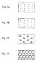
- An irregularly ordered arrangement or arraylacks a substantially non-random arrangement, spatial pattern or organizational structure in at least two dimension. For example, see FIG. 1B in which the nanostructures are aligned with respect to one another (e.g., the z-axis) but irregularly arranged on the x-y plane.
- matrixrefers to a material, often a polymeric material, into which a second material (e.g., a nanostructure) is embedded, surrounded, or otherwise associated.
- a matrixis typically composed of one or more monomers, but may include other matrix components/constituents. Often the matrix constituents include one or more “addressable” components or complementary binding pairs, e.g. that optionally promote assembly and/or cross-linkage of the matrix.
- Alignment ligandare components that interact with one or more nanostructures and can be used to order, orient and/or align the nanostructures associated therewith.
- the alignment ligands of the present inventionalso typically include one or more complementary binding pairs or specific or nonspecific “molecular recognition functionality” incorporated therein.
- An “array” of nanostructuresis an assemblage of nanostructures.
- the assemblagecan be spatially patterned or disordered.
- the arraycan form or comprise one or more functional elements (e.g., a junction or collection of junctions); alternatively, the array can be non-functional.
- the phrase “plurality of receiving structures”refers to the portions of the matrix that are structured to receive, position, and/or structurally order the nanostructures within the composition.
- the receiving structurestypically include cavities or void spaces into which the nanostructure is positioned; optionally, the receiving structures also include one or more functionalized chemical constituent that interacts with, associates with, binds to, or otherwise “receives,” the nanostructure.
- complementary binding pairrefers to a set of molecules that have an affinity for one another.
- the affinitycan be a non-specific molecular interaction, such as hydrogen boding between donor and acceptor molecules, or it can be a more complex or specific molecular recognition functionality, such as seen with a receptor and its complementary ligand.
- a complementary binding pair that employs a specific biochemical molecular recognition functionalityis also termed a “biomolecule pair” or “bioconjugate pair.”
- self organizing moleculerefers to a molecule that is capable of spontaneously assembling with other such molecules into stable, structured molecular aggregates or assemblages.
- One class of self-organizing moleculesare components used to prepare self assembling monolayers (SAMs).
- nanostructure binding componentand “head group” are used interchangeably herein to refer to various chemical constituents or moieties which are either coupled (e.g., in bound form) or capable of coupling (e.g. functionalized) to a nanostructure.
- the couplingcan be either directly to the surface of the nanostructure, or in some cases, the coupling is to a surface ligand associated with the nanostructure (e.g., the surface ligand functions as a linking group between the nanostructure and the component having the nanostructure binding component).
- An “aspect ratio”is the length of a first axis of a nanostructure divided by the average of the lengths of the second and third axes of the nanostructure, where the second and third axes are the two axes whose lengths are most nearly equal each other.
- the aspect ratio for a perfect rodwould be the length of its long axis divided by the diameter of a cross-section perpendicular to (normal to) the long axis.
- FIG. 1provides pictorial representations of various embodiments of a composition having a plurality of structurally ordered nanostructures in a matrix.
- FIG. 2provides a schematic representation of interactions between nanostructures and either monofunctional or multifunctional first and second alignment ligands as described in the present invention.
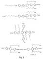
- FIG. 3depicts embodiments of alignment ligands for use in the present invention.
- the present inventionprovides compositions having structurally ordered nanostructures, as well as methods for preparing the nanostructures, and devices in which they can be employed. While the detailed description and examples focuses on one or another type of nanostructure, it will be appreciated that the methods and compositions provided herein can be applied to any of a number of nanostructures known in the art, including, but not limited to, nanocrystals, nanodots, quantum dots, nanoparticles, nanotubes, nanowires, nanoribbons, nanotetrapods, nanoscale branched structures (e.g., dendrimer branching structures), and the like.
- the present inventionprovides a plurality of structurally ordered nanostructures in a matrix.
- the structurally ordered nanostructuresare substantially non-randomly oriented nanostructures.
- the non-randomly oriented nanostructuresare substantially aligned with respect to one another, and/or substantially aligned with a selected axis (e.g., at least 25%, at least 50%, at least 75%, at least 90% or more of the nanostructures are substantially aligned with the selected axis).
- the selected axiscan be oriented substantially perpendicular to the surface of the substrate, parallel to the surface, or at a desired angle with respect to the surface.
- the nanostructuresare pointed in substantially the same direction.
- the nanostructuresare optionally oriented in the same direction.
- the present inventionprovides compositions having a plurality of non-randomly oriented nanostructures in a matrix.
- the oriented nanostructurescan be provided, for example, as a regularly-ordered array of nanostructures. Alternatively, the oriented nanostructures are provided as an irregularly ordered arrangement.
- the nanostructuresare typically oriented in relation to one another; (e.g., substantially parallel to one another, end to end, etc.); optionally, their orientation may also be described relative to a selected plane, space, or surface (e.g., parallel, perpendicular, at a selected angle, etc.).
- the non-random orientation of the nanostructuresis maintained by the presence of the matrix in which the nanostructures are disposed.
- FIG. 1Pictorial representations of exemplary embodiments of the present invention are provided in FIG. 1.
- nanorods-like structuresare depicted, along a z-axis (e.g., on end) in FIGS. 1A and 1B, angularly oriented in FIG. 1C, and arranged within the x-y plane in FIG. 1D.
- the present inventionis not limited to the embodiments shown.
- a plurality of substantially non-randomly oriented nanostructuresis depicted.
- the structuresare oriented with respect to a selected angle (e.g., 45°).
- the present inventionprovides compositions having a plurality of non-randomly oriented nanostructures in a matrix.
- the oriented nanostructurescan be provided, for example, as a regularly-ordered array of nanostructures. Alternatively, the oriented nanostructures are provided as an irregularly ordered arrangement.
- the nanostructuresare oriented in relation to one another; (e.g., parallel to one another, end to end, etc.); optionally, their orientation may also be described relative to a selected plane or surface (e.g., parallel, perpendicular, at a selected angle, etc.).
- the non-random orientation of the nanostructuresis maintained by the presence of the matrix in which the nanostructures are disposed.
- the present inventionprovides compositions having an array of nanostructures in a matrix, wherein the array comprises a plurality of non-randomly arranged nanostructure members.
- the nanostructure members of the arrayare also non-randomly oriented with respect to one another.
- FIG. 1 panel Aalso depicts a plurality of non-randomly arranged nanostructure members, in which the nanostructure members are also non-randomly oriented with respect to one another.
- FIG. 1, panel Cdepicts another embodiment of a composition having an array comprising a plurality of non-randomly arranged nanostructures. In this embodiment, the nanostructure members of the array are randomly oriented with respect to one another.
- FIG. 1, panel DA further embodiment of the array of non-randomly arranged nanostructures in a matrix is shown in FIG. 1, panel D, in which the nanostructure members are also non-randomly oriented with respect to one another.
- the nanostructuresare not parallel with one another, but are depicted as parallel with a planar surface such as a substrate.
- the compositions of the present inventionneed not be mainly 2-dimensional in nature. Further embodiments having 3-dimensional arrangements of nanostructures (for example, tetrameric and hexameric configurations, or other arrangements having interspersed sets of parallel nanostructural components) are also a feature of the present invention.
- the matrixis composed of one or more components that interact to form a plurality of receiving structures, which provides ordering and/or orientation to the nanostructures.
- the receiving structuretypically includes a pore-like cavity or void space in the matrix that can accommodate the selected nanostructure (e.g., a nanorod), the dimensions of which are determined by the selected matrix components used in the composition.
- the dimensions of the receiving structurescan be selected and/or adjusted based upon the nanostructure to be used in the composition, but typically will range in diameter from about 1-2 nm to about 500 nm (e.g., from about 1 nm to about 20 nm; or from about 10 nm to about 50 nm; or from about 100 nm to about 250 nm; or from about 250 nm to about 500 nm).
- the receiving structureoptionally includes a chemical moiety that has an affinity for the nanostructure, such as a nanostructure binding moiety.
- a nanostructure binding moietycan be used to assist in the assembly of the composition, particularly for nanostructures having a directionality or “end” arising, for example, from an asymmetrical composition or configuration of nanocrystal components.
- Association of the nanostructure with the receiving structure and/or nanostructure binding moiety thereinfurther provides for orientation and/or alignment of the nanostructures in the composition.
- the matrix components of the present inventionare modular in composition and synthesis, e.g., to provide varying sizes of receiving structures and/or varying nanostructure-binding functionalities based upon the specifics of the nanostructure to be incorporated into the composition.
- the matrix constituents of the present inventioninclude a core or body component (which optionally is a conductive chemical moiety, such as those described in Attorney Docket No. 40-0027-10US co-filed herewith), and one or more attached constituents.
- the body structurecan be either a conductive or a nonconductive chemical composition, depending in part upon the intended use of the nanostructure-containing composition. Often one or more “addressable” chemical constituents are attached to the body structure or otherwise incorporated into the matrix component.
- the addressable elementscan be used, for example, for connecting adjacent matrix monomers, e.g., to provide embodiments in which one or more components of the matrix are chemically crosslinked (or capable of chemically cross-linking) to one another.
- the addressable elements of the matrix monomersare designed to self-assemble to form the matrix.
- the matrix component(s)also optionally includes a nanostructure binding moiety (e.g., a functionalized “head group”) for coupling the matrix component to the nanostructure.
- a nanostructure binding moietye.g., a functionalized “head group”
- one or more components of the matrixare chemically cross-linked (or capable of chemically cross-linking) to the nanostructures of the composition.
- Exemplary embodiments of matrix components which can be used in the compositions and methods of the present inventionare provided in U.S.SNo. 60/452,232, as well as in Attorney Docket No. 40-002710US and international application Attorney Docket no. 40-002710PC by Whiteford et al., titled “Organic Species that Facilitate Charge Transfer to/from Nanocrystals” co-filed herewith.
- the matrixincludes one or more components having multiple nanostructure-binding components (i.e., multidentate components).
- the matrix componentincludes an additional “tail group” coupled to a portion (e.g., a terminus) of the body structure.
- the tail groupcan be designed to provide additional monomer coupling capacity, or additional nanostructure ligand binding capacity.
- compositions of the present inventionare comprised of two or more matrix layers, each member layer having a plurality of non-randomly oriented nanostructures.
- the orientation of member nanostructures in a first matrix layer with respect to the member nanostructures in an adjacent matrix layermay or may not be aligned with one another.
- member nanostructures in a first matrix layermay be aligned parallel (e.g., along the same orientation of direction) with respect to member nanostructures in the adjacent matrix layer.
- the member nanostructures in the two layerscan be perpendicular to one another, or differ in orientation by a selected angular degree (e.g., by 15°, 30°, 45°, 60° etc. with respect to one another).
- the member nanostructures in the layersare offset from one another (e.g., the layers of nanostructures are shifted in position, e.g., by a selected distance and/or controlled spacing), rather than being layered directly above one another.
- the member nanostructures in a first matrix layerare not aligned with respect to the member nanostructures in an adjacent matrix layer.
- the components used to prepare the matricescan be the same constituents, or they can be different matrix components.
- n-type nanostructuresare incorporated into one of the matrix layers (e.g., the first matrix layer), and p-type nanostructures are provided in the other (second) matrix layer.
- the two or more nanostructure-containing matrix layerscan be used to prepare templated nanostructure compositions, e.g., to form p-n junctions and the like.
- compositions of the present inventioncan be comprised of two or more matrix layers, in which each member layer includes a plurality of non-randomly arranged nanostructures within the constituent matrices.
- the present inventionalso provides methods of preparing a plurality of non-randomly oriented or non-randomly dispersed nanostructures in a matrix.
- the methodsinclude the steps of a) providing a plurality of nanostructures and a matrix composition, wherein the matrix composition comprises one or more matrix components that interact to form a plurality of receiving structures capable of accommodating the nanostructures; and b) heating and cooling the matrix composition in the presence of the plurality of nanostructures, thereby preparing the plurality of non-randomly oriented or non-randomly dispersed nanostructures in the matrix.
- the matrixis prepared from one or more components that interact to form a plurality of receiving structures (e.g., cavities or void spaces) that provide an ordering and/or orientation to the nanostructures.
- the configuration of the receiving structuresis used to determine to arrangement, ordering and/or orientation (e.g., alignment) of the incorporated nanostructures.
- the nanostructurescan be incorporated into the matrix either during (i.e., concomitant with) or after matrix formation.
- providing the matrix compositioninvolves providing one or more matrix components (i.e., monomers) in a non-ordered or non-polymerized form.
- Subsequent heating and cooling of the matrix composition in the presence of the plurality of nanostructuresallows the matrix to coalesce around the nanostructures, as a means of thermodynamically ordering the matrix around the plurality of nanostructures.
- the temperatures and reaction times employed in the methods of the present inventionwill vary with the selected matrix component, type of nanostructure, and the like, but could easily be determined by one of skill in the art without undue experimentation.
- the matrix (and the plurality of receiving structures therein)is assembled prior to exposure to the plurality of nanostructures. Heating and cooling the pre-formed matrix in the presence of the plurality of nanostructures provides allows the nanostructures to be inserted into one or more of the plurality of receiving structures.
- the matrix host spaceranges in diameter from about 1-2 nm to about 500 nm.
- the dimensionscan be further engineered to meet any requirements of the desired composition, e.g., based upon the size of the nanostructure.
- the surface of the nanostructure proximal to the host spacecan be functionalized to provide any of a number of selected chemical functionalities as receiving structures (e.g., for binding to the nanostructure).
- any of a number of matrix compositions known in the artcan be employed in the compositions and methods of the present invention.
- a wide variety of nanostructure-compatible polymersare known to those of skill in the art (see e.g., Demus et al. (ed.) 1998 Handbook of Liquid Crystals Volumes 1-4 (John Wiley and Sons, Inc., Hoboken, N.J.); Brandrup (ed.) 1999 Polymer Handbook, (John Wiley and Sons, Inc.); Harper 2002 Handbook of Plastics, Elastomers, and Composites, 4th edition (McGraw-Hill, Columbus, Ohio); and Kraft et al. (1998) Angew. Chem. Int. Ed. 37:402-428.
- Exemplary polymers for use in the present inventioninclude, but are not limited to, thermoplastic polymers (e.g., polyolefins, polyesters, polysilicones, polyacrylonitrile resins, polystyrene resins, polyvinyl chloride, polyvinylidene chloride, polyvinyl acetate, or fluoroplastics); thermosetting polymers (e.g., phenolic resins, urea resins, melamine resins, epoxy resins, polyurethane resins); engineering plastics (e.g., polyamides, polyacrylate resins, polyketones, polyimides, polysulfones, polycarbonates, polyacetals); and liquid crystal polymers, including main chain liquid crystal polymers (e.g., poly(hydroxynapthoic acid)) and side chain liquid crystal polymers (e.g., poly [n-((4′(4′′-cyanphenyl)phenoxy)alkyl)vinyl ether]).
- Certain embodimentsinclude conductive organic polymers; see e.g. T. A. Skatherin (ed.) 1986 Handbook of Conducting Polymers I. (Marcel Dekker, New York).
- conductive polymers for use as matrices of the present inventioninclude, but are not limited to, poly(3-hexylthiophene) (P3HT), poly[2-methoxy, 5-(2′-ethyl-hexyloxy)-p-phenylene-vinylene] (MEH-PPV), poly(p-phenylene vinylene) (PPV), and polyaniline.
- Conductive compositions as provided in U.S.SNo. 60/452,232 and Attorney Docket No. 40-002710US, co-filed herewith,can also be used as matrix components of the present invention.
- the conductive compositionscontain a conjugated organic species and at least one binding group capable of interacting with a nanostructure surface; during use, the compositions are coupled via the binding group to the nanostructure surface, such that the compositions are substantially conductive to electrons and/or holes being transported by/through the nanostructure (e.g., during the process of extracting or injecting the electrons or holes).
- compositions of the present inventioncan optionally be derivatized with additional chemical groups, e.g., to modulate the electronic conjugation of the core organic species, to couple or align adjacent nanostructures, to provide additional chemical functionalities in the matrix receiving structures, or to facilitate dispersion, mixing and/or blending of nanostructures in various matrices.
- additional chemical groupse.g., to modulate the electronic conjugation of the core organic species, to couple or align adjacent nanostructures, to provide additional chemical functionalities in the matrix receiving structures, or to facilitate dispersion, mixing and/or blending of nanostructures in various matrices.
- conductive compositionsthat include a conjugated organic species as a body structure, coupled to a nanostructure-binding head group, an alkyne-containing tail group, and addressable sidechain elements for crosslinking or coupling of the compositions, can be used as matrix components in the present invention.
- one or more components of the matrixare chemically crosslinked, or are capable of chemically cross-linking to one another.
- Traditional methods of crosslinkinginclude, but are not limited to, various condensation reactions, free radical curing (e.g., via ultraviolet light, electron beam or peroxides), thermal curing, and amine crosslinking using Michael Addition reaction chemistry.
- the cross linkagesare typically generated through one or more functionalized moieties coupled to the body structure of the matrix (e.g., sidechains).
- the matrix componentscan include photolabile groups that, once activated by exposure to light, can be removed to expose a reactive site for cross-linking adjacent matrix monomers.
- photolabile groups and their associated linkage chemistriesare well known in the art.
- the cross-linker groupis capped by a protecting group that is cleaved or rendered cleavable upon exposure to light of a desired wavelength.
- photolabile protecting groupsinclude nitroveratryloxycarbonyl protecting groups, such as NVOC and MeNVOC, as well as nitropiperonyloxycarbonyl protecting groups, such as NPOC and MeNPOC, and others, e.g., PyMOC.
- the use of these protecting groups and others in, for example, photolithographic activation of surfaces,is described in, e.g., U.S. Pat. No. 5,489,678 and U.S. Pat. No. 6,147,205.
- the photo-removable protecting groupexposed an amine moiety, which then can react with a proximal activated carboxylic acid to form the cross-linkage.
- One exemplary chemical moiety that can be used to connect adjacent matrix componentsis a diacetylene group.
- any of a number of conjugation reagentssuch as zero-length cross linkers, homobifunctional cross-linkers, heterobifunctional cross-linkers, and the like, are known in the art and can be incorporated into the matrix components of the present invention (see, for example, Hermanson (1996) Bioconjugate Techniques, Academic Press, New York; and Brandrup (1999) The Polymer Handbook, 4th Edition, John Wiley & Sons, Ltd, New York, N.Y.).
- one or more components of the matrixare optionally chemically cross-linked or capable of chemically cross-linking to one or more of the nanostructures, via one or more functionalized “head groups” (e.g., nanostructure binding groups).
- head groupse.g., nanostructure binding groups.
- exemplary chemical moieties for use as functionalized head groups in the present inventioninclude, but are not limited to, phosphonic acid, carboxylic acid, amine, phosphine, phosphine oxide, carbamate, isocyanate, nitro, salen, dithiolene, catechol, N,O-chelate ligand, P,N-chelate ligand, and/or thiol moieties.
- ureaderivatives of nanocrystal growth terminators, or other nitrogen-containing aromatic compounds or heterocycles (e.g., various amides, imidazoles, benzoimidazoles, pyridines, pyrimidines, purines, or quinolines) can also be used as nanostructure-binding head group moieties in the compositions and methods of the present invention.
- nitrogen-containing aromatic compounds or heterocyclese.g., various amides, imidazoles, benzoimidazoles, pyridines, pyrimidines, purines, or quinolines
- Exemplary compoundsinclude, but are not limited to, derivatives of 2-aminopyridine, 3-aminopyridine, 1,2-diaminopyridine, and other compounds commonly used as inorganic nitrogen-containing ligands.
- the nanostructure binding head groupsmay be in an ionizable form, such that under certain conditions, e.g., low or high pH, the functional group has substantial affinity for the nanostructure, e.g., a strong positive or negative charge, while under different environmental conditions, the affinity is substantially lower, or is even negative.
- the functionalized (or bound) head groupis a monodentate structure (e.g., includes a single moiety capable of interacting with the nanocrystal).
- the head groupis a multidentate structure capable of a plurality of interactions with the nanostructure surface, or a ligand associated with the nanostructure surface.
- the present inventionalso provides a plurality of non-randomly oriented or non-randomly dispersed nanostructures in a matrix as prepared by a method provided herein.
- the present inventionprovides compositions having a plurality of selectively-oriented nanostructures in which the members nanostructures are associated with one or more alignment ligands.
- the alignment ligandsare molecules that have one or more chemical or biochemical functionalities that have an attraction for one another.
- a portion of a first alignment ligand on a first nanostructureinteracts with a complementary portion of a second alignment ligand on an adjacent member nanostructure.
- Multiple alignment ligandsare associated with each nanostructure, each of which can independently interact with a complementary alignment ligands on adjacent nanostructures; these interactions can be used to generate (and/or maintain) the selective orientation of the population of nanostructures (e.g., providing structural order to the nanostructures).
- an entropy increasewill also be gained upon heating and cooling as solvent molecules are ejected from the void space between matrices by forming a host(matrix)-guest(nanocrystal or nanowire) or inclusion molecule with the nanowire/nanocrystal, thereby preferring the ordered array.
- This nanowire/nanocrystal-matrix inclusion complexwill also increase crystallinity of the entire system thereby imparting stability to the preferred ordered structure and driving the equilibrium towards the ordered array.
- the first and second alignment ligandsare molecules which have selected molecular recognition functionalities or moieties.
- the molecular recognition between the first and second alignment ligandscan be a simple chemical interaction, such as the hydrogen bonding interaction that occurs between an amine moiety and a hydroxyl moiety.
- Alignment ligandscan be designed to take advantage of any of a number of basic molecular interactions beyond hydrogen bonding.
- coulombic interactionscan be employed for complex formation between the first and second alignment ligands.
- the interactionscan be of varying number (monodentate or multidentate) and varying strength (weak, intermediate or strong), but typically the interactions are reversible, at least during initial formation of the composition.
- Conductive compositions as provided in U.S.SNo. 60/452,232 and Attorney Docket No. 40-002710US co-filed herewithcan be used, or modified for use, as alignment ligands of the present invention.
- conductive compositionsthat include either a non-conjugated or a conjugated organic species as a body structure, coupled to a nanostructure-binding head group, an alkyne tail group having a second nanostructure-binding moiety, and two sidechains (coupled to the body structure) incorporating complementary binding moieties (e.g., an amine moiety and a hydroxyl moiety) can be used in the methods, devices and compositions of the present invention.
- complementary binding moietiese.g., an amine moiety and a hydroxyl moiety
- compositions for use as alignment ligandsare shown in FIG. 3.
- methylene, aryl, acetylene and alkene groupscan be incorporated into the alignment composition (e.g., within the head group, tail group or sidechain moieties), the more “floppy” constituents (e.g., methylenes) typically produce less conductive compositions and/or less thermodynamically predictable compositions.
- Bioconjugate/biomolecular pairsprovide another example of complementary molecular recognition moieties which can be used in the present invention.
- Various biomolecular pairings and interactionsare described in detail in, for example, Bioconjugate Techniques by Hermanson (1996, Academic Press, New York).
- Any of a number of complementary biomolecules known in the artcan be used as the first and second alignment ligands.
- the interaction between an antibody and an antigen that binds to the antibodycan be used to orient adjacent nanostructures, as can the interaction between: biotin and avidin or streptavidin; a lectin and a carbohydrate ligand; or a protein (e.g., a receptor) and the complementary ligand.
- Even complementary nucleic acids, and/or an aptamer and an aptamer ligandcan be employed as alignment ligands in the present invention.
- one of the alignment ligandscan be a moiety used to functionalize the surface of the nanostructure (e.g., via silanation, nitridation, or a flnctionalizing plasma such as described in PCT/US03/09827 to Empedocles).
- the first and/or second alignment ligandhas more than one molecular recognition functionality per ligand (e.g., a multifunctional or multidentate ligand).
- a multidentate alignment ligandcan have multiple amine functionalities, or multiple copies of biotin attached to a core structure.
- the alignment ligandcan be multifunctional by having both halves (complements) of the selected conjugating embodiment; e.g., both a biotin moiety and an avidin moiety.
- the first and second alignment ligandsare provided by the same molecule.
- a schematic representation of exemplary monofunctional and multifunctional alignment ligand embodimentsare provided in FIG. 2.
- Molecular self assemblyis the spontaneous organization of selected molecules into organized two-dimensional (or three-dimensional) configurations based upon intermolecular interactions such as those described herein.
- Organization of the alignment ligand:nanostructure compositionoptimally leads to a thermodynamic minimum.
- Complementary binding of alignment ligands, as well as the presence of the nanostructures filling void spaces within the matrix (and thereby ejecting solvent molecules to compensate for entropy loss while increasing crytallinity of the system) and the binding of nanostructures by head attachment groupsresults in an overall reduction of Gibbs free energy and a thermodynamically favored equilibrium.
- the alignment ligandsare associated either directly with the nanostructure surface, or with other ligands already associated or bound to the nanostructure surface.
- the alignment ligandsfurther include one or more functionalized head group(s) capable of binding to a nanostructure surface or to a ligand associated with a nanostructure surface.
- the head group functionality selected for use in the compositionwill depend in part upon the type of nanostructure being aligned.
- Exemplary chemical moieties which can be used to couple the alignment ligand to the nanostructure surfaceinclude, but are not limited to, phosphonic acid, carboxylic acid, amine, phosphine, phosphine oxide, carbamate, urea, pyridine, isocyanate, amide, nitro, pyrimidine, imidazole, salen, dithiolene, catechol, N,O-chelate ligand, P,N-chelate ligand, thiol, or a combination of these moieties.
- a chelating P,N ligandincludes a phosphorous heteroatom and a nitrogen heteroatom capable of bonding or binding through a lone pair of electrons that may form a hydrogen, coordination or covalent bond.
- Exemplary chelating P,N ligandsinclude 2-triphenyl phosphino-pyridine, 2-triethyl phosphino-aniline, diphenylphosphino ethyl amine
- a Chelating N,O ligandincludes a nitrogen heteroatom and an oxygen heteroatom capable of bonding or binding through a lone pair of electrons that may form a hydrogen, coordination or covalent bond.
- Exemplary chelating N,O ligandsinclude ethanol amine and aniline phosphinate, as well as 2-hydroxyaniline, 3,5-diaminobenzoic acid, guanine (G), cytosine (C), and G ⁇ circumflex over ( ) ⁇ C bicyclic bases (see, for example, Fenniri et al. “Entropically driven self-assembly of multichannel rosette nanotubes” presented at the Arthur M. Sackler Colloquium of the National Academy of Sciences, May 18-20, 2001).
- Nanostructure:alignment ligand compositionsare also provided in the present invention.
- the distance between adjacent nanostructuresis determined in part by the composition and conformation of the associated alignment ligand.
- the adjacent nanostructuresor vectors representing adjacent nanostructures
- do not deviate in distancee.g. the span between the adjacent nanostructures by more than about 10%, or optionally, by more than about 5%.
- the present inventionalso provides methods for preparing a plurality of selectively-oriented nanostructures, in which the nanostructure population includes a first set of nanostructures associated with a first alignment ligand, and a second set of nanostructures associated with a second alignment ligand.
- any of a number of embodiments of alignment ligandscan be used to prepare the selectively-oriented nanostructures, such as those depicted in FIG. 3.
- the first and second alignment ligandsare distinct chemical entities (FIG. 3, panel A), while in other embodiments, a single multifunctional molecule acts as both the first alignment ligand and the second alignment ligand (FIG. 3, panel B).
- the first alignment ligandcan include a biotin moiety, while the complementary second alignment ligand has an avidin moiety incorporated into the structure.
- biotin and avidin functionalitiescan be incorporated into two separate ligand molecules; alternatively, they can be two portions of a multifunctional ligand molecule (e.g., a single alignment ligand has both molecular recognition functionalities incorporated therein).
- the first set of nanostructuresfurther includes the second alignment ligand and the second set of nanostructures also includes the first alignment ligand (FIG. 3, panel C).
- dual alignment functionality of a given nanostructurecan also be achieved, for example, by positioning one or more first alignment ligands along one portion of a given nanostructure, and second alignment ligand(s) along a second portion of the nanostructure (FIG. D).
- the alignment ligandsare coupled to the nanostructures, either via direct coupling to the nanostructure surface, or to an additional (e.g. intervening) ligand associated with the nanostructure.
- the first alignment ligands on the first set of nanostructureare then interacted with the second alignment ligand on a second adjacent nanostructure, to selectively orient the plurality of nanostructures.
- a plurality of nanowiresare prepared for use as the plurality of nanostructures, by any of a number of techniques known in the art, such as vapor deposition, or solution deposition.
- alternative nanostructure embodimentsnanonocrystals, nanodots, nanorods, etc.
- the nanostructuresare then treated, e.g., by vapor phase depositing the first alignment ligand on a surface of a first portion of the plurality of nanostructures; and vapor phase depositing the second alignment ligand on a surface of a second portion of the plurality of nanostructures.
- the methodsfurther include the step of removing the nanowire-alignment ligand conjugates from the substrate prior to interacting the first and second alignment ligands.
- the first and second portions of the nanowireare separate populations of nanowires.
- the alignment ligandis not a monofunctional ligand (i.e., having only one of the complementary molecular recognition elements)
- the methodgenerates two populations of ligand-associated nanostructures.
- the first and second portionscomprise separate regions of individual nanowires, for example, two termini of the nanostructures, a single (non-symmetrical) population of nanowires is generated.
- the first and second alignment ligandscomprise molecules incorporating a selected molecular interaction (e.g., hydrogen bond formation), a selected molecular recognition functionality (e.g., a biomolecular pair) or other self organizing molecules.
- a selected molecular interactione.g., hydrogen bond formation
- a selected molecular recognition functionalitye.g., a biomolecular pair
- the first and second alignment ligands which can be designed to interact via hydrogen bondinginclude, but are not limited to, an amine-containing compound and an alcohol-containing compound.
- the methods of the present inventioninclude the step of coupling the alignment ligands to the surface of the associated nanostructures.
- alignment ligands having a functionalized head group or other nanostructure-binding moietyare employed, for binding the alignment molecule to the nanostructure surface.
- Exemplary chemical functionalities which interact with nanostructure surfacesinclude, but are not limited to, phosphonic acid, carboxylic acid, amine, phosphine, phosphine oxide, carbamate, urea, pyridine, isocyanate, amide, nitro, pyrimidine, imidazole, salen, dithiolene, catechol, N,O-chelate ligand, P,N-chelate ligand, thiol moieties (or combinations thereof).
- the first and second alignment ligandsfurther comprise a crosslinking or polymerizable element, such that interacting the first and second alignment ligands leads to crosslinking or polymerization of the first and second alignment ligands.
- interacting the first and second alignment ligandsis performed by heating and cooling the plurality of nanostructures.
- interacting the first and second ligandscan be achieved by mixing the ligands with solvents in which the ligands have different solubilities (e.g., due to polarity).
- solventsthat can be used include, but are not limited to, chloroform, toluene, and chlorobenzene.
- the methods of the present inventionfurther include the step of affixing the plurality of selectively-oriented nanostructures to a substrate.
- the first and second alignment ligandscan optionally be removed.
- the present inventionalso provides a plurality of clusters of selectively-oriented nanostructures on a substrate. Unlike the previously-described embodiments of the present invention, these clusters are provided independent of surrounding matrix.
- the orientation of the selectively-oriented nanostructurescan be perpendicular to a surface or other defined x,y plane with which the nanostructures are associated, or the orientation can be an orientation other than normal to the surface or plane.
- the clusters of selectively-oriented nanostructurescan be generated, for example, to provide an aggregation of functional elements such as junctions at defined locations on a substrate, e.g., for interfacing with additional nanoscale or microscale electronics).
- nanostructures(or combination of nanostructures) can be used in the compositions and methods of the present invention, including, but not limited to, nanocrystals, nanodots, nanospheres, nanorods, nanowires, nanoribbons, nanotetrapods, various branched structures (e.g., dendrimer branching structures), quantum dots, and the like.
- nanostructuresare prepared from semiconductive materials.
- Semiconductor nanostructuresinclude a wide range of different materials that exist as nano-sized particles or structures, e.g., having at least one cross sectional dimension of less than about 500 nm, and preferably, less than 100 nm. These nanostructures may be comprised of a wide range of semiconductive materials, including for example, group III-V, group II-VI and group IV semiconductors or alloys of these materials. For example, CdSe, CdTe, InP, InAs, CdS, ZnS, ZnO, ZnSe, PbSe, PbS, and/or PbTe semiconductors, or their alloys, are optionally used as at least a portion of the nanostructure component.
- nanowiresinclude semiconductor nanowires as described in Published International Patent Application Nos. WO 02/17362 to Lieber et al. (“Doped elongated semiconductors, growing such semiconductors, devices including such semiconductors and fabricating such devices”), WO 02/48701 to Lieber et al. (“Nanosensors”), and WO 01/03208 to Lieber et al. (“Nanoscopic Wire-based devices, arrays, and methods of their manufacture”), carbon nanotubes, and other elongated conductive or semiconductive structures of like dimensions.
- Nanostructurescomprised of semiconductor material selected from, e.g., Si, Ge, Sn, Se, Te, B, Diamond, P, B—C, B—P(BP6), B—Si, Si—C, Si—Ge, Si—Sn and Ge—Sn, SiC, BN/BP/BAs, AlN/AlP/AlAs/AlSb, GaN/GaP/GaAs/GaSb, InN/InP/InAs/InSb, BN/BP/BAs, AlN/AlP/AlAs/AlSb, GaN/GaP/GaAs/GaSb, InN/InP/InAs/InSb, ZnO/ZnS/ZnSe/ZnTe, CdS/CdSe/CdTe, HgS/HgSe/HgTe, BeS/BeSe/BeTe/MgS/MgSe, GeS, Ge
- the semiconductormay also include a dopant from a group consisting of: a p-type dopant from Group III of the periodic table; an n-type dopant from Group V of the periodic table; a p-type dopant selected from a group consisting of: B, Al and In; an n-type dopant selected from a group consisting of: P, As and Sb; a p-type dopant from Group II of the periodic table; a p-type dopant selected from a group consisting of: Mg, Zn, Cd and Hg; a p-type dopant from Group IV of the periodic table; a p-type dopant selected from a group consisting of: C and Si.; or an n-type is selected from a group consisting of: Si, Ge, Sn, S, Se and Te.
- nanostructurese.g., by patterning nanostructure catalysts and/or precursors on a substrate, oriented growth in magnetic fields, use of fluidic assembly arrays, and radially deposition of nanostructures on a substrate.
- VLSvapor liquid solid growth
- laser ablationlaser catalytic growth
- thermal evaporationvapor liquid solid growth
- VLSlaser ablation
- PDA-CVDhybrid pulsed laser ablation/ chemical vapor deposition
- substrates and self assembling monolayer (SAM) forming materialscan be used, e.g., along with microcontact printing techniques to make nanostructures, such as those described by Schön, Meng, and Bao (2001) “Self-assembled monolayer organic field-effect transistors” Nature 413:713; Zhou et al. (1997) “Nanoscale Metal/Self-Assembled Monolayer/Metal Heterostructures” Applied Physics Letters 71:611; and WO 96/29629 (Whitesides, et al., published Jun. 26, 1996).
- SAMself assembling monolayer
- a preferred embodiment of a composition that can be used to prepare a self-assembled monolayertypically includes a thiol component that can be attached to a substrate (e.g., gold) and one or more aliphatic chains that interact and pack to form an organized layer.
- a substratee.g., gold
- nanostructuressuch as nanowires having various aspect ratios, including nanowires with controlled diameters, is described in, e.g., Gudiksen et al (2000) “Diameter-selective synthesis of semiconductor nanowires” J. Am. Chem. Soc. 122:8801-8802; Cui et al. (2001) “Diameter-controlled synthesis of single-crystal silicon nanowires” Appl. Phys. Lett. 78: 2214-2216; Gudiksen et al. (2001) “Synthetic control of the diameter and length of single crystal semiconductor nanowires” J. Phys. Chem. B 105:4062-4064; Morales et al.
- the aligned and/or oriented nanostructures of the present inventioncan be used or assembled into any of a number of functional elements or devices.
- a variety of methods of making one-dimensional structures for use in small scale devices and device elements and methods of making junctions and circuits of such deviceshave been described. or example, nanostructures such as nanowires and nanotubes can transport electrons and holes, providing the building blocks for nanoscale electronic devices. Studies of charge carrying properties of such elements have led to the creation of field effect transistors, single electron transistors, rectifying junctions, and even complete circuits.
- Nanostructures or nanostructure arrays made according to the present inventionoptionally can similarly be configured as memory, logic, computing elements, or the like.
- Kitswill optionally additionally comprise instructions for preparing the structurally ordered nanostructures, nanostructure:matrix compositions, or nanostructure:alignment ligand compositions of the present invention, instructions for incorporating the compositions into nanostructure-containing devices, or instructions for otherwise performing the methods provided herein, packaging materials, one or more containers which contain nanostructures, matrix components, or alignment ligands, and/or the like.
- kits embodying the methods and devices hereinoptionally comprise one or more of the following: (1) one or more alignment ligands, or components for the synthesis of the alignment ligands; (2) one or more preparations of nanostructures; (3) components and/or instructions for the preparation of structurally ordered nanostructures in a matrix; (4) components and/or instructions for the preparation of nanostructure:alignment ligand compositions; (5) components and/or instructions for the preparation of clusters of ordered nanostructures; (6) instructions for practicing the methods described herein; and/or (7) packaging materials.
- the present inventionprovides for the use of any component or kit herein, for the practice of any method or assay herein, and/or for the use of any apparatus or kit to practice any assay or method herein.
Landscapes
- Chemical & Material Sciences (AREA)
- Engineering & Computer Science (AREA)
- Nanotechnology (AREA)
- Crystallography & Structural Chemistry (AREA)
- Physics & Mathematics (AREA)
- Condensed Matter Physics & Semiconductors (AREA)
- Theoretical Computer Science (AREA)
- Composite Materials (AREA)
- Mathematical Physics (AREA)
- General Physics & Mathematics (AREA)
- Materials Engineering (AREA)
- Investigating, Analyzing Materials By Fluorescence Or Luminescence (AREA)
- Manufacture Of Metal Powder And Suspensions Thereof (AREA)
- Inorganic Insulating Materials (AREA)
- Compositions Of Oxide Ceramics (AREA)
- Luminescent Compositions (AREA)
- Medicinal Preparation (AREA)
Abstract
Description
- This application is related to U.S. provisional applications U.S.SNo. 60/408,722, filed Sep. 5, 2002; U.S.SNo. 60/421,353, filed Oct. 25, 2002; U.S.SNo. 60/452,038, filed Mar. 4, 2003; and U.S.SNo. 60/452,232, filed Mar. 4, 2003. The present application claims priority to and benefit of each of these prior applications, which are hereby incorporated herein by reference in their entirety for all purposes.[0001]
- The present invention is in the field of nanotechnology. More particularly, the present invention is directed to structurally ordered nanostructure compositions (e.g., non-randomly oriented and/or arranged nanostructures), as well as related methods for producing, and related devices.[0002]
- Nanostructures such as nanotubes, nanocrystals, and nanowires have gained a great deal of attention for their interesting and novel properties in electrical, chemical, optical and other applications. Such nanomaterials have a wide variety of expected and actual uses, including use as semiconductors for nanoscale electronics, optoelectronic applications in emissive devices (e.g., lasers, LEDs, etc.), light collectors, photovoltaics, and sensor applications (see, for example international applications PCT/US03/09827 filed Mar. 1, 2003, PCT/US03/09991 filed Mar. 1, 2003 and Attorney Docket No. 40-001320PC co-filed herewith; PCT publication WO 03/005450; and U.S. Pat. No. 5,230,957; U.S. Pat. No. 5,537,000; U.S. Pat. No. 5,990,479; U.S. Pat. No. 6,198,655; and U.S. Pat. No. 6,207,229).[0003]
- While commercial applications of the molecular, physical, chemical and optical properties of these materials have been postulated, generating commercially viable products has not, as yet, been forthcoming. In the world of devices with integrated nanostructure elements, some of the difficulties in producing commercially viable products has stemmed from the difficulty in handling and interfacing with such small scale materials. For example, existing nanocrystal-based photovoltaic device technologies suffer from inefficient charge transfer from the nanostructure surface to the electrode of the photovoltaic device. One limiting factor in the electron/hole transport is the degree of nanocrystal packing and ordering. For the most part, the nanostructures are produced in bulk as free-standing elements that must be positioned and/or oriented within the photovoltaic device, a task which has proven difficult. While a variety of procedures for making nanostructures are available, current technologies are insufficient to produce selectively-oriented or arranged arrays of nanostructures.[0004]
- Accordingly, there exists a need in the art for non-randomly oriented nanostructures and/or non-randomly-arranged nanostructures, as well as methods for preparing non-randomly oriented or non-randomly dispersed nanostructures, for example, within a matrix. The present invention meets these and a variety of other needs. A complete understanding of the invention will be obtained upon review of the following.[0005]
- The present invention provides compositions of structurally ordered nanostructures, as well as methods for preparing structurally ordered nanostructures. Any of a number of nanostructures (or combination of nanostructures) can be used in the compositions and methods of the present invention, including, but not limited to, nanocrystals, nanospheres, nanorods, nanowires, nanoribbons, nanotetrapods, various branched structures (e.g., dendrimer branching structures), quantum dots, nanodots, and the like.[0006]
- In one aspect, the present invention provides a plurality of structurally ordered nanostructures in a matrix. In one embodiment, the structurally ordered nanostructures are substantially non-randomly oriented nanostructures. Optionally, the non-randomly oriented nanostructures are substantially aligned with respect to one another, and/or substantially aligned with a selected axis. For compositions that are associated with or otherwise proximal to a substrate, the axis can be selected to be oriented substantially perpendicular to the surface of the substrate, parallel to the surface, or at a desired angle with respect to the surface.[0007]
- In another aspect of the present invention, the plurality of structurally ordered nanostructures provide a substantially regularly-ordered array of nanostructures. Alternatively, the structurally ordered nanostructures are provided as an irregularly-ordered arrangement of structurally ordered nanostructures.[0008]
- Nanostructures for use in the compositions of the present invention are available in a variety of available shapes, such as spherical, ovoid, elongated or branched structures. For example, the structurally ordered nanostructures can be nanocrystals, nanodots, nanospheres, nanorods, nanowires, nanotetrapods, dendrimer branching structures, or any combination thereof. Preferably, the nanostructures are inorganic nanostructures, such as conductive nanostructures or semiconductive nanostructures.[0009]
- Optionally, the matrix used in the compositions of the present invention have one or more components that interact to form a plurality of receiving structures that provide an ordering and/or an orientation to the nanostructures. In some embodiments, self-organizing molecules, such as those used to prepare self assembling monolayers, are used as components of the matrix. Furthermore, in some embodiments, one or more components of the matrix can be chemically crosslinked to one another or polymerized (e.g., during or after formation of the nanostructure-containing matrix).[0010]
- Optionally, one or more components of the matrix can also be crosslinked to one or more of the nanostructures, or to a surface ligand associated with the nanostructures (e.g., an intervening component, such as a surfactant). In some embodiments, the matrix components provide multiple functionalities for binding to the nanostructure(s).[0011]
- In some embodiments of the present invention, two or more matrix layers are present in the nanostructure-containing composition. Preferably, each member layer contains a plurality of structurally ordered nanostructures. The member nanostructures in a first matrix layer may or may not aligned with respect to the member nanostructures in the adjacent matrix layer.[0012]
- In a further aspect, the present invention provides compositions having a plurality of structurally ordered nanostructures, wherein members nanostructures comprise one or more alignment ligands associated with the nanostructures. The structurally ordered nanostructures are typically substantially non-randomly oriented nanostructures. Optionally, the structurally ordered nanostructures are substantially aligned nanostructures.[0013]
- The structurally ordering of the plurality of nanostructures is achieved by interacting a first alignment ligand on a first member nanostructure with a second alignment ligand on an adjacent member nanostructure. Typically, the first and second alignment ligands are complementary binding pairs. Optionally, both complements of the binding pair are provided on the same molecule (e.g., a multifunctional molecule). In some embodiments, a single chemical entity can be used as the first and second alignment ligands. Alternatively, the two halves of the complementary binding pair can be provided on different compositions, such that the first and second alignment ligands are differing molecules.[0014]
- In a preferred embodiment, the first and second alignment ligands are self-organizing molecules. For example, alignment ligands can be generated using self assembling monolayer components.[0015]
- Typically, the complementary binding pairs employed in the alignment ligands are molecules having a molecular recognition functionality. For example, the alignment ligands can include an amine-containing compound and a ketone or alcohol-containing compound. Alternatively, one or more biomolecule pairs can be used as the alignment ligands. Exemplary biomolecule pairs include, but are not limited to, an antibody and an antigen that binds to the antibody; biotin and avidin (or streptavidin); a lectin and a carbohydrate ligand; complementary nucleic acids; a protein and a ligand; a receptor and a ligand; an aptamer and an aptamer ligand. Furthermore, combinations of biomolecules can be employed. In one embodiment, the first alignment ligand and/or the second alignment ligand comprise two or more selected molecular recognition functionalities per alignment ligand.[0016]
- The alignment ligands can be associated (either directly or indirectly) with any of a number of nanostructure shapes and sizes, such as spherical, ovoid, elongated or branched structures. For example, nanostructures can be nanocrystals, nanospheres, nanorods, nanowires, nanotetrapods, dendrimer branching structures, or any combination thereof. Preferably, the nanostructures are inorganic nanostructures, such as conductive nanostructures or semiconductive nanostructures. The alignment ligand can either be directly associated with the surface of a nanostructure, or indirectly associated, through a surface ligand on the nanostructure; this interaction can be, for example, an ionic interaction, a covalent interaction, a hydrogen bond interaction, an electrostatic interaction, a coulombic interaction, a van der Waals force interaction, or a combination thereof. Optionally, the chemical composition of the first and/or second alignment ligands includes one or more functionalized head group capable of binding to a nanostructure surface, or to an intervening surface ligand. Chemical functionalities that can be used as a functionalized head group in the present invention include, but are not limited to, one or more phosphonic acid, carboxylic acid, amine, phosphine, phosphine oxide, carbamate, urea, pyridine, isocyanate, amide, nitro, pyrimidine, imidazole, salen, dithiolene, catechol, N,O-chelate ligand (such as ethanol amine or aniline phosphinate), P,N-chelate ligand, and/or thiol moieties.[0017]
- In a further aspect, the present invention provides a plurality of clusters of structurally ordered nanostructures (for example, substantially aligned nanostructures) on a substrate. The nanostructures can be positioned, e.g., substantially perpendicular to the plane of the substrate, substantially parallel to the substrate, or at another selected angle. Furthermore, the substrate can be planar, curved, or can comprise more complex two or three dimensional geometries. Optionally, the position or orientation of the nanostructure is selected such that clusters of nanostructures are tuned; this can be achieved, e.g., by selecting an appropriate atom geometry and/or chemical composition (see, for example, Huang et al. (2003) “From 1D chain to 3D network: Tuning hybrid II-VI nanostructures and their optical properties”[0018]J. Am. Chem. Soc.125:7049-7055). Optionally, the atom geometry is tetrahedral, square, planar, octahedral, or another selected configuration.
- The present invention also provides methods for preparing aligned, oriented, arranged, or otherwise structurally ordered nanostructures. In some embodiments of the methods of the present invention, a plurality of non-randomly oriented or non-randomly dispersed nanostructures in a matrix are prepared by a) providing a plurality of nanostructures and a matrix composition, in which the matrix composition includes one or more matrix components that interact to form a plurality of receiving structures capable of accommodating the nanostructures; and b) heating and cooling the matrix composition in the presence of the plurality of nanostructures, thereby preparing the plurality of non-randomly oriented or non-randomly dispersed nanostructures in the matrix.[0019]
- In one embodiment, the matrix composition is provided as one or more matrix components or monomers in a non-ordered (e.g., unassembled) form; the process of heating and cooling the matrix composition in the presence of the plurality of nanostructures allows for thermodynamic ordering of the matrix around the plurality of nanostructures, thereby preparing an ordered nanostructure-containing matrix.[0020]
- In an alternate embodiment, the matrix composition is provided as a pre-formed matrix having the plurality of receiving structures capable of accommodating the nanostructures. Heating and cooling the matrix composition in the presence of the plurality of nanostructures provides the energy necessary to insert the nanostructures into the receiving structures of the matrix.[0021]
- In another embodiment of the present invention, methods for preparing a plurality of selectively-oriented nanostructures are provided. The methods include the steps of: a) providing a plurality of nanostructures comprising a first set of nanostructures associated with a first alignment ligand and a second set of nanostructures associated with a second alignment ligand; and b) interacting the first alignment ligand on a first nanostructure with the second alignment ligand on a second adjacent nanostructure, to selectively orient the plurality of nanostructures. Optionally, the first and second alignment ligands are complementary binding pairs, which can be presented on separate molecules or on differing portions of the same molecule.[0022]
- Preferably, the first and/or second alignment ligands are physically coupled (e.g., bonded) to the nanostructure surface (or to a molecule associated with the surface). Typically, this interaction is through a portion of the alignment ligand having a nanostructure binding moiety or functionalized head group of the present invention.[0023]
- The nanostructures employed in the methods of the present invention (e.g., nanorods, nanowires, etc) can be prepared by any of a number of techniques, such as vapor deposition or solution phase deposition onto a substrate. The member nanostructures are then treated with the alignment ligands. For example, after preparing a plurality of nanostructures, the first alignment ligand is vapor phase deposited on a surface of a first portion of the plurality of nanostructures; and the second alignment ligand is vapor phase deposited on a surface of a second portion of the plurality of nanostructures. The nanostructure-alignment ligand conjugates are then allowed to interact, to drive the orientation of the nanostructures. If the nanostructures were synthesized on a substrate, the nanostructure-alignment ligand conjugates are optionally removed from the substrate.[0024]
- Optionally, the first and second alignment ligands are complementary binding pairs selected for a particular molecular recognition functionality or moiety. The complementary binding pairs can provide a simple chemical interaction, such as the hydrogen bonding between an amine moiety and a ketone/alcohol moiety, or a more complex interaction, such as seen with biomolecule/bioconjugate pairs. A preferred set of molecular recognition functionalities are embodied in the class of compounds termed “self organizing molecules.”[0025]
- Interacting the first and second alignment ligands to achieve the selective orientation of the plurality of nanostructures, can be performed, for example, by heating and cooling the plurality of nanostructures. In embodiments in which the first and second alignment ligands further include a crosslinking or polymerizable element, interacting the alignment ligands optionally includes the step of crosslinking or polymerizing the first and second alignment ligands, e.g., to form a matrix.[0026]
- As a further embodiment of the methods of the present invention, the plurality of selectively-oriented nanostructures can be affixed to a substrate or surface. Optionally, the first and second alignment ligands are removed after affixing the aligned nanostructures, to produce a plurality of selectively-oriented nanostructures on a substrate.[0027]
- Any of a number of nanostructures known in the art can be used in the methods, including, but not limited to, nanocrystals, nanodots, nanospheres, nanorods, nanowires, nanotetrapods, various branching structures, or combinations thereof. The present invention also provides the plurality of selectively oriented, non-randomly oriented, or non-randomly dispersed nanostructures as prepared by the described methods.[0028]
- The aligned and/or organized nanostructures can be used in any of a number of devices and applications, including, but not limited to, various photovoltaic devices, optoelectronic devices (LEDs, lasers, optical amplifiers), light collectors, photodetectors and/or the like.[0029]
- Before describing the present invention in detail, it is to be understood that this invention is not limited to particular devices or biological systems, which can, of course, vary. It is also to be understood that the terminology used herein is for the purpose of describing particular embodiments only, and is not intended to be limiting. As used in this specification and the appended claims, the singular forms “a”, “an” and “the” include plural referents unless the content clearly dictates otherwise. Thus, for example, reference to “a substrate” optionally includes a combinations of two or more substrates; reference to “nanowire” optionally includes mixtures of nanowires, and the like.[0030]
- Unless defined otherwise, all technical and scientific terms used herein have the same meaning as commonly understood by one of ordinary skill in the art to which the invention pertains. Although any methods and materials similar or equivalent to those described herein can be used in the practice for testing of the present invention, the preferred materials and methods are described herein. In describing and claiming the present invention, the following terminology will be used in accordance with the definitions set out below.[0031]
- As used herein, the term “nanostructures” refers to structures having at least one region or characteristic dimension with a dimension of less than 500 nm, e.g., less than 200 nm, less than 100 nm, less than 50 nm, or even less than 20 nm. Typically, the region or characteristic dimension will be along the smallest axis of the structure. Examples of such structures include various spherical, ovoid, elongated or branched structures, including, but not limited to, nanocrystals, nanowires, nanorods, nanotubes, branched nanowires, nanotetrapods, nanotripods, nanobipods, nanodots, quantum dots, nanoparticles, nanoribbons, and/or the like. Nanostructures can be substantially homogeneous in material properties, or in certain embodiments can be heterogeneous (e.g. heterostructures). Optionally, a nanostructure can comprise one or more surface ligands (for example, surfactants). The nanostructure is optionally substantially single crystal in structure (a “single crystal nanostructure” or a “monocrystalline nanostructure”). While nanostructures for use in the present invention can be fabricated from essentially any convenient material or material, preferably the nanostructure is prepared from an inorganic compound, a conductive material, and/or a semiconductive material. A conductive or semi-conductive nanostructure often displays 1-dimensional quantum confinement, e.g., an electron can often travel along only one dimension of the structure.[0032]
- The terms “crystalline” or “substantially crystalline”, when used with respect to nanostructures, refer to the fact that the nanostructures typically exhibit long-range ordering across one or more dimensions of the structure. It will be understood by one of skill in the art that the term “long range ordering” will depend on the absolute size of the specific nanostructures, as ordering for a single crystal cannot extend beyond the boundaries of the crystal. In this case, “long-range ordering” will mean substantial order across at least the majority of the dimension of the nanostructure. In some instances, a nanostructure can bear an oxide or other coating, or can be comprised of a core and at least one shell. In such instances it will be appreciated that the oxide, shell(s), or other coating need not exhibit such ordering (e.g. it can be amorphous, polycrystalline, or otherwise). In such instances, the phrase “crystalline,” “substantially crystalline,” “substantially monocrystalline,” or “monocrystalline” refers to the central core of the nanostructure (excluding the coating layers or shells). The terms “crystalline” or “substantially crystalline” as used herein are intended to also encompass structures comprising various defects, stacking faults, atomic substitutions, and the like, as long as the structure exhibits substantial long range ordering (e.g., order over at least about 80% of the length of at least one axis of the nanostructure or its core). In addition, it will be appreciated that the interface between a core and the outside of a nanostructure or between a core and an adjacent shell or between a shell and a second adjacent shell may contain non-crystalline regions and may even be amorphous. This does not prevent the nanostructure from being crystalline or substantially crystalline as defined herein.[0033]
- The term “monocrystalline” when used with respect to a nanostructure indicates that the nanostructure is substantially crystalline and comprises substantially a single crystal. When used with respect to a nanostructure heterostructure comprising a core and one or more shells, “monocrystalline” indicates that the core is substantially crystalline and comprises substantially a single crystal.[0034]
- A “nanocrystal” is a nanostructure that is substantially monocrystalline. Nanocrystals typically have an aspect ratio between about 0.1 and about 1.5 (e.g., between about 0.1 and about 0.5, between about 0.5 and about 1, or between about 1 and about 1.5). Thus, nanocrystals include, for example, substantially spherical nanocrystals with aspect ratios between about 0.8 and about 1.2 and disk-shaped nanocrystals. Nanocrystals typically have a diameter between about 1.5 nm and about 15 nm (e.g., between about 2 nm and about 5 nm, between about 5 nm and about 10 nm, or between about 10 nm and about 15 nm). Nanocrystals can be substantially homogeneous in material properties, or in certain embodiments can be heterogeneous (e.g. heterostructures). The term “nanocrystal” is intended to encompass substantially monocrystalline nanostructures comprising various defects, stacking faults, atomic substitutions, and the like, as well as substantially monocrystalline nanostructures without such defects, faults, or substitutions. In the case of nanocrystal heterostructures comprising a core and one or more shells, the core of the nanocrystal is substantially monocrystalline, but the shell(s) need not be. The nanocrystals can be fabricated from essentially any convenient material or materials. The nanocrystals can comprise “pure” materials, substantially pure materials, doped materials and the like, and can include insulators, conductors, and semiconductors.[0035]
- A “nanowire” is a nanostructure that has one principle axis that is longer than the other two principle axes. Consequently, the nanowire has an aspect ratio greater than one; nanowires of this invention have an aspect ratio greater than about 1.5 or greater than about 2. Short nanowires, sometimes referred to as “nanorods,” typically have an aspect ratio between about 1.5 and about 10 (e.g., greater than 1.5, or greater than 5). Longer nanowires have an aspect ratio greater than about 10, greater than about 20, greater than about 50, or greater than about 100, or even greater than about 10,000. The diameter of a nanowire is typically less than about 500 nm, preferably less than about 200 nm, more preferably less than about 150 nm, and most preferably less than about 100 nm, about 50 nm, or about 25 nm, or even less than about 10 nm or about 5 nm. The length of a nanowire is optionally greater than about 100 nm, e.g., greater than 200 nm, greater than 500 nm, or even greater than 1000 nm.[0036]
- The nanowires employed in the present invention can be substantially homogeneous in material properties, or in certain embodiments can be heterogeneous (e.g. nanowire heterostructures). The nanowires can be fabricated from essentially any convenient material or materials, and can be, e.g., substantially crystalline, substantially monocrystalline, polycrystalline, or amorphous. The nanowires can comprise “pure” materials, substantially pure materials, doped materials and the like, and can include insulators, conductors, and semiconductors. Nanowires can have a variable diameter or can have a substantially uniform diameter, that is, a diameter that shows a variance less than about 20% (e.g., less than about 10%, less than about 5%, or less than about 1%) over the region of greatest variability and over a linear dimension of at least 5 nm (e.g., at least 10 nm, at least 20 nm, or at least 50 nm). Typically the diameter is evaluated away from the ends of the nanowire (e.g. over the central 20%, 40%, 50%, or 80% or more of the nanowire). A nanowire can be straight or can be e.g. curved or bent, over the entire length of its long axis or a portion thereof. In certain embodiments, a nanowire or a portion thereof can exhibit two- or three-dimensional quantum confinement. Nanowires according to this invention can expressly exclude carbon nanotubes, and, in certain embodiments, exclude “whiskers” or “nanowhiskers”, particularly whiskers having a diameter greater than 100 nm, or greater than about 200 nm. Nanorods, nanowires nanocomposites, and other nanostructures are described in additional detail in U.S.SNo. 60/408,722, filed Sep. 5, 2002, the contents of which are incorporated herein in their entirety.[0037]
- The phrase “structurally ordered nanostructures” as used herein refers to nanostructures that are substantially organized, ordered, aligned or otherwise “substantially non-random” either with respect to each other or with respect to a given axis or spatial position. A “plurality of structurally ordered nanostructures” is intended to include sets of non-randomly arrayed nanostructures (e.g., clustered, patterned or other spatially-organized arrangements of either aligned, oriented or non-oriented nanostructures), as well as sets of non-randomly oriented nanostructures (in which the majority of individual nanostructures are substantially non-random, but can be positioned in either regularly patterned arrays or irregular, e.g., scattered, arrangements).[0038]
- The phrase “substantially non-random” (as used herein to describe the orientation and/or spatial arrangement of nanostructures) indicates that the nanostructures do not occupy a purely random distribution of orientations or spatial positioning with respect to each other. A collection of nanostructures is “substantially non-randomly oriented” if, when the position of each nanostructure is represented as a vector of a unit length in a three-dimensional rectangular coordinate system, at least one component of the vector average of the nanostructures' orientations is non-zero (when representing a nanostructure by a vector, any intrinsic difference between the two ends of the nanostructure can typically be ignored). For example, the nanostructures dispersed in a matrix (e.g., members of the plurality of structurally ordered nanostructures) would have substantially nonrandom orientations if a higher percentage of the nanostructures pointed in one direction (or in one of at least two specific directions) than in any other direction (e.g., if at least 10%, at least 25%, at least 50%, at least 75%, at least 90% or more of the nanostructures pointed in a particular direction). As another example, the plurality of nanorods or nanowires in a matrix would be substantially non-randomly oriented if a majority of the nanostructures had their long axes more nearly perpendicular than parallel to a surface of the film (or vice versa). The nanostructures can be substantially non-randomly oriented, yet not point in at least one specific direction. The preceding examples are for illustration only; a collection of nanostructures could possess less order than these examples yet still be substantially non-randomly oriented.[0039]
- The term “substantially oriented nanostructures” or “substantially non-randomly oriented nanostructures” as used herein refers to sets or clusters of nanostructures in which at least 10%, at least 25%, at least 50%, at least 75%, at least 90% or more of the member nanostructures are oriented or positioned relative to a designated axis, plane, surface or three dimensional space. The orientation or positioning can be, for example, substantially parallel, substantially perpendicular, or at a selected angle (e.g., about 15°, 30°, 45°, or 60°). Substantially oriented nanostructures include, for example, sets of splayed or angularly-gathered sets of nanostructures (e.g., star patterns or hexagonal groupings) as well as substantially aligned populations of nanostructures.[0040]
- The term “substantially aligned” as used herein refers to a subset of oriented nanostructures, in which at least 10%, at least 25%, at least 50%, at least 75%, at least 90% or more of the member nanostructures are oriented or positioned in a co-axial or parallel relationship, e.g., with one another as well as being oriented relative to the designated axis, plane or surface. For example, a plurality or set of substantially aligned nanostructures are positioned in a like manner with respect to one another such that the vectors representing the long axes of the member nanostructures differ from one another by no more than about 30° (e.g., the vectors are within about 30°, or preferably within about 15°, or more preferably within about 10° or within about 5° of one another).[0041]
- The terms substantially perpendicular” and “substantially parallel” refers to orientations (or vectors representing populations of orientations) that vary by less than 25%, preferably by less than 10%, and more preferably by less than 5% from a perpendicular or parallel vector, respectively.[0042]
- The term “about” refers to an acceptable variation of less than 25%, preferably less than 10%, and more preferably less than 5% of the cited value.[0043]
- The phrase “regularly ordered” as used herein refers to a substantially non-random arrangement, spatial pattern or organizational structure in either two dimensions or three dimensions. An irregularly ordered arrangement or array lacks a substantially non-random arrangement, spatial pattern or organizational structure in at least two dimension. For example, see FIG. 1B in which the nanostructures are aligned with respect to one another (e.g., the z-axis) but irregularly arranged on the x-y plane.[0044]
- The term “matrix” refers to a material, often a polymeric material, into which a second material (e.g., a nanostructure) is embedded, surrounded, or otherwise associated. A matrix is typically composed of one or more monomers, but may include other matrix components/constituents. Often the matrix constituents include one or more “addressable” components or complementary binding pairs, e.g. that optionally promote assembly and/or cross-linkage of the matrix.[0045]
- “Alignment ligand” are components that interact with one or more nanostructures and can be used to order, orient and/or align the nanostructures associated therewith. In addition to having an affinity for a nanostructure, the alignment ligands of the present invention also typically include one or more complementary binding pairs or specific or nonspecific “molecular recognition functionality” incorporated therein.[0046]
- An “array” of nanostructures is an assemblage of nanostructures. The assemblage can be spatially patterned or disordered. Optionally, the array can form or comprise one or more functional elements (e.g., a junction or collection of junctions); alternatively, the array can be non-functional.[0047]
- As used herein, the phrase “plurality of receiving structures” refers to the portions of the matrix that are structured to receive, position, and/or structurally order the nanostructures within the composition. The receiving structures typically include cavities or void spaces into which the nanostructure is positioned; optionally, the receiving structures also include one or more functionalized chemical constituent that interacts with, associates with, binds to, or otherwise “receives,” the nanostructure.[0048]
- The term “complementary binding pair” refers to a set of molecules that have an affinity for one another. The affinity can be a non-specific molecular interaction, such as hydrogen boding between donor and acceptor molecules, or it can be a more complex or specific molecular recognition functionality, such as seen with a receptor and its complementary ligand. A complementary binding pair that employs a specific biochemical molecular recognition functionality is also termed a “biomolecule pair” or “bioconjugate pair.”[0049]
- The term “self organizing molecule” refers to a molecule that is capable of spontaneously assembling with other such molecules into stable, structured molecular aggregates or assemblages. One class of self-organizing molecules are components used to prepare self assembling monolayers (SAMs).[0050]
- The terms “nanostructure binding component” and “head group” are used interchangeably herein to refer to various chemical constituents or moieties which are either coupled (e.g., in bound form) or capable of coupling (e.g. functionalized) to a nanostructure. The coupling can be either directly to the surface of the nanostructure, or in some cases, the coupling is to a surface ligand associated with the nanostructure (e.g., the surface ligand functions as a linking group between the nanostructure and the component having the nanostructure binding component).[0051]
- An “aspect ratio” is the length of a first axis of a nanostructure divided by the average of the lengths of the second and third axes of the nanostructure, where the second and third axes are the two axes whose lengths are most nearly equal each other. For example, the aspect ratio for a perfect rod would be the length of its long axis divided by the diameter of a cross-section perpendicular to (normal to) the long axis.[0052]
- FIG. 1 provides pictorial representations of various embodiments of a composition having a plurality of structurally ordered nanostructures in a matrix.[0053]
- FIG. 2 provides a schematic representation of interactions between nanostructures and either monofunctional or multifunctional first and second alignment ligands as described in the present invention.[0054]
- FIG. 3 depicts embodiments of alignment ligands for use in the present invention.[0055]
- The present invention provides compositions having structurally ordered nanostructures, as well as methods for preparing the nanostructures, and devices in which they can be employed. While the detailed description and examples focuses on one or another type of nanostructure, it will be appreciated that the methods and compositions provided herein can be applied to any of a number of nanostructures known in the art, including, but not limited to, nanocrystals, nanodots, quantum dots, nanoparticles, nanotubes, nanowires, nanoribbons, nanotetrapods, nanoscale branched structures (e.g., dendrimer branching structures), and the like.[0056]
- Structurally Ordered Nanostructures in a Matrix[0057]
- In one aspect, the present invention provides a plurality of structurally ordered nanostructures in a matrix. In one embodiment, the structurally ordered nanostructures are substantially non-randomly oriented nanostructures. Optionally, the non-randomly oriented nanostructures are substantially aligned with respect to one another, and/or substantially aligned with a selected axis (e.g., at least 25%, at least 50%, at least 75%, at least 90% or more of the nanostructures are substantially aligned with the selected axis). For example, for compositions that are associated with or otherwise proximal to a substrate, the selected axis can be oriented substantially perpendicular to the surface of the substrate, parallel to the surface, or at a desired angle with respect to the surface. Optionally, the nanostructures are pointed in substantially the same direction. For example, for compositions including asymmetric nanostructure elements, the nanostructures are optionally oriented in the same direction.[0058]
- In one embodiment, the present invention provides compositions having a plurality of non-randomly oriented nanostructures in a matrix. The oriented nanostructures can be provided, for example, as a regularly-ordered array of nanostructures. Alternatively, the oriented nanostructures are provided as an irregularly ordered arrangement. The nanostructures are typically oriented in relation to one another; (e.g., substantially parallel to one another, end to end, etc.); optionally, their orientation may also be described relative to a selected plane, space, or surface (e.g., parallel, perpendicular, at a selected angle, etc.). The non-random orientation of the nanostructures is maintained by the presence of the matrix in which the nanostructures are disposed.[0059]
- Pictorial representations of exemplary embodiments of the present invention are provided in FIG. 1. In these embodiment, nanorods-like structures are depicted, along a z-axis (e.g., on end) in FIGS. 1A and 1B, angularly oriented in FIG. 1C, and arranged within the x-y plane in FIG. 1D. However, the present invention is not limited to the embodiments shown. A plurality of substantially non-randomly oriented nanostructures is depicted. In a particular embodiment, rather than substantially aligning the nanostructures with one another, the structures are oriented with respect to a selected angle (e.g., 45°).[0060]
- Optionally, the present invention provides compositions having a plurality of non-randomly oriented nanostructures in a matrix. The oriented nanostructures can be provided, for example, as a regularly-ordered array of nanostructures. Alternatively, the oriented nanostructures are provided as an irregularly ordered arrangement. The nanostructures are oriented in relation to one another; (e.g., parallel to one another, end to end, etc.); optionally, their orientation may also be described relative to a selected plane or surface (e.g., parallel, perpendicular, at a selected angle, etc.). The non-random orientation of the nanostructures is maintained by the presence of the matrix in which the nanostructures are disposed.[0061]
- In another aspect, the present invention provides compositions having an array of nanostructures in a matrix, wherein the array comprises a plurality of non-randomly arranged nanostructure members. Optionally, the nanostructure members of the array are also non-randomly oriented with respect to one another. Thus, FIG. 1 panel A also depicts a plurality of non-randomly arranged nanostructure members, in which the nanostructure members are also non-randomly oriented with respect to one another. FIG. 1, panel C depicts another embodiment of a composition having an array comprising a plurality of non-randomly arranged nanostructures. In this embodiment, the nanostructure members of the array are randomly oriented with respect to one another. A further embodiment of the array of non-randomly arranged nanostructures in a matrix is shown in FIG. 1, panel D, in which the nanostructure members are also non-randomly oriented with respect to one another. In this embodiment, the nanostructures are not parallel with one another, but are depicted as parallel with a planar surface such as a substrate. The compositions of the present invention need not be mainly 2-dimensional in nature. Further embodiments having 3-dimensional arrangements of nanostructures (for example, tetrameric and hexameric configurations, or other arrangements having interspersed sets of parallel nanostructural components) are also a feature of the present invention.[0062]
- In a preferred embodiment of the present invention, the matrix is composed of one or more components that interact to form a plurality of receiving structures, which provides ordering and/or orientation to the nanostructures. The receiving structure typically includes a pore-like cavity or void space in the matrix that can accommodate the selected nanostructure (e.g., a nanorod), the dimensions of which are determined by the selected matrix components used in the composition. As such, the dimensions of the receiving structures can be selected and/or adjusted based upon the nanostructure to be used in the composition, but typically will range in diameter from about 1-2 nm to about 500 nm (e.g., from about 1 nm to about 20 nm; or from about 10 nm to about 50 nm; or from about 100 nm to about 250 nm; or from about 250 nm to about 500 nm).[0063]
- The receiving structure optionally includes a chemical moiety that has an affinity for the nanostructure, such as a nanostructure binding moiety. The presence of a nanostructure binding moiety can be used to assist in the assembly of the composition, particularly for nanostructures having a directionality or “end” arising, for example, from an asymmetrical composition or configuration of nanocrystal components. Association of the nanostructure with the receiving structure and/or nanostructure binding moiety therein further provides for orientation and/or alignment of the nanostructures in the composition.[0064]
- Typically, the matrix components of the present invention are modular in composition and synthesis, e.g., to provide varying sizes of receiving structures and/or varying nanostructure-binding functionalities based upon the specifics of the nanostructure to be incorporated into the composition. Typically, the matrix constituents of the present invention include a core or body component (which optionally is a conductive chemical moiety, such as those described in Attorney Docket No. 40-0027-10US co-filed herewith), and one or more attached constituents. The body structure can be either a conductive or a nonconductive chemical composition, depending in part upon the intended use of the nanostructure-containing composition. Often one or more “addressable” chemical constituents are attached to the body structure or otherwise incorporated into the matrix component. The addressable elements (e.g., sidechains, or “side arms”) can be used, for example, for connecting adjacent matrix monomers, e.g., to provide embodiments in which one or more components of the matrix are chemically crosslinked (or capable of chemically cross-linking) to one another. In some embodiments, the addressable elements of the matrix monomers are designed to self-assemble to form the matrix.[0065]
- The matrix component(s) also optionally includes a nanostructure binding moiety (e.g., a functionalized “head group”) for coupling the matrix component to the nanostructure. In some embodiments of the compositions, one or more components of the matrix are chemically cross-linked (or capable of chemically cross-linking) to the nanostructures of the composition. Exemplary embodiments of matrix components which can be used in the compositions and methods of the present invention are provided in U.S.SNo. 60/452,232, as well as in Attorney Docket No. 40-002710US and international application Attorney Docket no. 40-002710PC by Whiteford et al., titled “Organic Species that Facilitate Charge Transfer to/from Nanocrystals” co-filed herewith.[0066]
- Optionally, the matrix includes one or more components having multiple nanostructure-binding components (i.e., multidentate components). As an example, in some compositions of the present invention, the matrix component includes an additional “tail group” coupled to a portion (e.g., a terminus) of the body structure. The tail group can be designed to provide additional monomer coupling capacity, or additional nanostructure ligand binding capacity.[0067]
- In a further embodiment, the compositions of the present invention are comprised of two or more matrix layers, each member layer having a plurality of non-randomly oriented nanostructures. The orientation of member nanostructures in a first matrix layer with respect to the member nanostructures in an adjacent matrix layer may or may not be aligned with one another. For example, member nanostructures in a first matrix layer may be aligned parallel (e.g., along the same orientation of direction) with respect to member nanostructures in the adjacent matrix layer. Alternatively, the member nanostructures in the two layers can be perpendicular to one another, or differ in orientation by a selected angular degree (e.g., by 15°, 30°, 45°, 60° etc. with respect to one another). Optionally, the member nanostructures in the layers are offset from one another (e.g., the layers of nanostructures are shifted in position, e.g., by a selected distance and/or controlled spacing), rather than being layered directly above one another. Alternatively, the member nanostructures in a first matrix layer are not aligned with respect to the member nanostructures in an adjacent matrix layer. The components used to prepare the matrices can be the same constituents, or they can be different matrix components. Optionally, n-type nanostructures are incorporated into one of the matrix layers (e.g., the first matrix layer), and p-type nanostructures are provided in the other (second) matrix layer. The two or more nanostructure-containing matrix layers can be used to prepare templated nanostructure compositions, e.g., to form p-n junctions and the like.[0068]
- Furthermore, the compositions of the present invention can be comprised of two or more matrix layers, in which each member layer includes a plurality of non-randomly arranged nanostructures within the constituent matrices.[0069]
- Methods of Preparing a Nanostructure-Matrix Composition[0070]
- As a further aspect, the present invention also provides methods of preparing a plurality of non-randomly oriented or non-randomly dispersed nanostructures in a matrix. The methods include the steps of a) providing a plurality of nanostructures and a matrix composition, wherein the matrix composition comprises one or more matrix components that interact to form a plurality of receiving structures capable of accommodating the nanostructures; and b) heating and cooling the matrix composition in the presence of the plurality of nanostructures, thereby preparing the plurality of non-randomly oriented or non-randomly dispersed nanostructures in the matrix.[0071]
- In a preferred embodiment of the present invention, the matrix is prepared from one or more components that interact to form a plurality of receiving structures (e.g., cavities or void spaces) that provide an ordering and/or orientation to the nanostructures. The configuration of the receiving structures is used to determine to arrangement, ordering and/or orientation (e.g., alignment) of the incorporated nanostructures. In the methods of the present invention, the nanostructures can be incorporated into the matrix either during (i.e., concomitant with) or after matrix formation. For example, in one embodiment of the methods, providing the matrix composition involves providing one or more matrix components (i.e., monomers) in a non-ordered or non-polymerized form. Subsequent heating and cooling of the matrix composition in the presence of the plurality of nanostructures allows the matrix to coalesce around the nanostructures, as a means of thermodynamically ordering the matrix around the plurality of nanostructures. The temperatures and reaction times employed in the methods of the present invention will vary with the selected matrix component, type of nanostructure, and the like, but could easily be determined by one of skill in the art without undue experimentation. Standard protocols for preparation of matrices can be found, for example, in Nalwa (2001)[0072]Advanced Functional Molecules and Polymersvolumes 1-4; Kroschwitz et al., (1990)Concise Encyclopedia of Polymer Science and Engineering(Wiley-Interscience, New York, N.Y.); Chandrasekhar (1999)Conducting Polymers, Fundamentals and Applications: A Practical Approach(Academic Publishers, Boston, Mass., 1999); and Brandrup (1999) Polymer Handbook, 4th Edition (John Wiley & Sons, Ltd, New York, N.Y.), which references are incorporated herein in their entirety.
- In an alternative embodiment, the matrix (and the plurality of receiving structures therein) is assembled prior to exposure to the plurality of nanostructures. Heating and cooling the pre-formed matrix in the presence of the plurality of nanostructures provides allows the nanostructures to be inserted into one or more of the plurality of receiving structures. Typically, the matrix host space ranges in diameter from about 1-2 nm to about 500 nm. However, the dimensions can be further engineered to meet any requirements of the desired composition, e.g., based upon the size of the nanostructure. Furthermore, the surface of the nanostructure proximal to the host space can be functionalized to provide any of a number of selected chemical functionalities as receiving structures (e.g., for binding to the nanostructure).[0073]
- Any of a number of matrix compositions known in the art can be employed in the compositions and methods of the present invention. For example, a wide variety of nanostructure-compatible polymers are known to those of skill in the art (see e.g., Demus et al. (ed.) 1998[0074]Handbook of Liquid CrystalsVolumes 1-4 (John Wiley and Sons, Inc., Hoboken, N.J.); Brandrup (ed.) 1999Polymer Handbook,(John Wiley and Sons, Inc.); Harper 2002Handbook of Plastics, Elastomers, and Composites,4th edition (McGraw-Hill, Columbus, Ohio); and Kraft et al. (1998)Angew. Chem. Int. Ed.37:402-428.
- Exemplary polymers for use in the present invention include, but are not limited to, thermoplastic polymers (e.g., polyolefins, polyesters, polysilicones, polyacrylonitrile resins, polystyrene resins, polyvinyl chloride, polyvinylidene chloride, polyvinyl acetate, or fluoroplastics); thermosetting polymers (e.g., phenolic resins, urea resins, melamine resins, epoxy resins, polyurethane resins); engineering plastics (e.g., polyamides, polyacrylate resins, polyketones, polyimides, polysulfones, polycarbonates, polyacetals); and liquid crystal polymers, including main chain liquid crystal polymers (e.g., poly(hydroxynapthoic acid)) and side chain liquid crystal polymers (e.g., poly [n-((4′(4″-cyanphenyl)phenoxy)alkyl)vinyl ether]). Certain embodiments include conductive organic polymers; see e.g. T. A. Skatherin (ed.) 1986[0075]Handbook of Conducting Polymers I.(Marcel Dekker, New York). Examples of conductive polymers for use as matrices of the present invention include, but are not limited to, poly(3-hexylthiophene) (P3HT), poly[2-methoxy, 5-(2′-ethyl-hexyloxy)-p-phenylene-vinylene] (MEH-PPV), poly(p-phenylene vinylene) (PPV), and polyaniline.
- Conductive compositions as provided in U.S.SNo. 60/452,232 and Attorney Docket No. 40-002710US, co-filed herewith, can also be used as matrix components of the present invention. The conductive compositions contain a conjugated organic species and at least one binding group capable of interacting with a nanostructure surface; during use, the compositions are coupled via the binding group to the nanostructure surface, such that the compositions are substantially conductive to electrons and/or holes being transported by/through the nanostructure (e.g., during the process of extracting or injecting the electrons or holes). The compositions of the present invention can optionally be derivatized with additional chemical groups, e.g., to modulate the electronic conjugation of the core organic species, to couple or align adjacent nanostructures, to provide additional chemical functionalities in the matrix receiving structures, or to facilitate dispersion, mixing and/or blending of nanostructures in various matrices. For example, conductive compositions that include a conjugated organic species as a body structure, coupled to a nanostructure-binding head group, an alkyne-containing tail group, and addressable sidechain elements for crosslinking or coupling of the compositions, can be used as matrix components in the present invention.[0076]
- Optionally, one or more components of the matrix are chemically crosslinked, or are capable of chemically cross-linking to one another. Traditional methods of crosslinking include, but are not limited to, various condensation reactions, free radical curing (e.g., via ultraviolet light, electron beam or peroxides), thermal curing, and amine crosslinking using Michael Addition reaction chemistry. The cross linkages are typically generated through one or more functionalized moieties coupled to the body structure of the matrix (e.g., sidechains). In addition to traditional crosslinking agents like acrylates and methacrylates, the matrix components can include photolabile groups that, once activated by exposure to light, can be removed to expose a reactive site for cross-linking adjacent matrix monomers. A wide variety of photolabile groups and their associated linkage chemistries are well known in the art. For example, the cross-linker group is capped by a protecting group that is cleaved or rendered cleavable upon exposure to light of a desired wavelength. Examples of known photolabile protecting groups include nitroveratryloxycarbonyl protecting groups, such as NVOC and MeNVOC, as well as nitropiperonyloxycarbonyl protecting groups, such as NPOC and MeNPOC, and others, e.g., PyMOC. The use of these protecting groups and others in, for example, photolithographic activation of surfaces, is described in, e.g., U.S. Pat. No. 5,489,678 and U.S. Pat. No. 6,147,205. Optionally, the photo-removable protecting group exposed an amine moiety, which then can react with a proximal activated carboxylic acid to form the cross-linkage.[0077]
- One exemplary chemical moiety that can be used to connect adjacent matrix components is a diacetylene group. However, any of a number of conjugation reagents, such as zero-length cross linkers, homobifunctional cross-linkers, heterobifunctional cross-linkers, and the like, are known in the art and can be incorporated into the matrix components of the present invention (see, for example, Hermanson (1996)[0078]Bioconjugate Techniques,Academic Press, New York; and Brandrup (1999)The Polymer Handbook,4th Edition, John Wiley & Sons, Ltd, New York, N.Y.).
- In addition, one or more components of the matrix are optionally chemically cross-linked or capable of chemically cross-linking to one or more of the nanostructures, via one or more functionalized “head groups” (e.g., nanostructure binding groups). Exemplary chemical moieties for use as functionalized head groups in the present invention include, but are not limited to, phosphonic acid, carboxylic acid, amine, phosphine, phosphine oxide, carbamate, isocyanate, nitro, salen, dithiolene, catechol, N,O-chelate ligand, P,N-chelate ligand, and/or thiol moieties.[0079]
- Alternatively, urea, derivatives of nanocrystal growth terminators, or other nitrogen-containing aromatic compounds or heterocycles (e.g., various amides, imidazoles, benzoimidazoles, pyridines, pyrimidines, purines, or quinolines) can also be used as nanostructure-binding head group moieties in the compositions and methods of the present invention. Exemplary compounds include, but are not limited to, derivatives of 2-aminopyridine, 3-aminopyridine, 1,2-diaminopyridine, and other compounds commonly used as inorganic nitrogen-containing ligands.[0080]
- In alternative arrangements, the nanostructure binding head groups may be in an ionizable form, such that under certain conditions, e.g., low or high pH, the functional group has substantial affinity for the nanostructure, e.g., a strong positive or negative charge, while under different environmental conditions, the affinity is substantially lower, or is even negative.[0081]
- In some embodiments, the functionalized (or bound) head group is a monodentate structure (e.g., includes a single moiety capable of interacting with the nanocrystal). In an alternate embodiment, the head group is a multidentate structure capable of a plurality of interactions with the nanostructure surface, or a ligand associated with the nanostructure surface.[0082]
- The present invention also provides a plurality of non-randomly oriented or non-randomly dispersed nanostructures in a matrix as prepared by a method provided herein.[0083]
- Nanostructures with Interacting Alignment Ligands[0084]
- In another aspect, the present invention provides compositions having a plurality of selectively-oriented nanostructures in which the members nanostructures are associated with one or more alignment ligands. The alignment ligands are molecules that have one or more chemical or biochemical functionalities that have an attraction for one another. Typically, a portion of a first alignment ligand on a first nanostructure interacts with a complementary portion of a second alignment ligand on an adjacent member nanostructure. Multiple alignment ligands are associated with each nanostructure, each of which can independently interact with a complementary alignment ligands on adjacent nanostructures; these interactions can be used to generate (and/or maintain) the selective orientation of the population of nanostructures (e.g., providing structural order to the nanostructures).[0085]
- The thermodynamic expression ΔG=ΔH−TΔS describes the relationship between enthalpy (ΔH) and entropy (ΔS) relating to Gibb's free energy (ΔG). Heating and cooling of the composition allow the entropy term (ΔS) to be used to overcome the energy barrier (ΔH) in breaking up random binding of complementary pairs. The complementary binding pairs can then overcome the energy barrier preventing the thermodynamically-favored ordered array binding. Further, an entropy increase will also be gained upon heating and cooling as solvent molecules are ejected from the void space between matrices by forming a host(matrix)-guest(nanocrystal or nanowire) or inclusion molecule with the nanowire/nanocrystal, thereby preferring the ordered array. This nanowire/nanocrystal-matrix inclusion complex will also increase crystallinity of the entire system thereby imparting stability to the preferred ordered structure and driving the equilibrium towards the ordered array.[0086]
- Typically, the first and second alignment ligands are molecules which have selected molecular recognition functionalities or moieties. As one example, the molecular recognition between the first and second alignment ligands can be a simple chemical interaction, such as the hydrogen bonding interaction that occurs between an amine moiety and a hydroxyl moiety. Thus, any of a variety of amine-containing compounds and alcohol-containing compounds can be employed as first and second alignment ligands in the present invention. Alignment ligands can be designed to take advantage of any of a number of basic molecular interactions beyond hydrogen bonding. For example, coulombic interactions, van der Waals forces, ionic interactions, covalent bond formation, and/or various hydrophobic or hydrophilic interactions can be employed for complex formation between the first and second alignment ligands. The interactions can be of varying number (monodentate or multidentate) and varying strength (weak, intermediate or strong), but typically the interactions are reversible, at least during initial formation of the composition.[0087]
- Conductive compositions as provided in U.S.SNo. 60/452,232 and Attorney Docket No. 40-002710US co-filed herewith can be used, or modified for use, as alignment ligands of the present invention. For example, conductive compositions that include either a non-conjugated or a conjugated organic species as a body structure, coupled to a nanostructure-binding head group, an alkyne tail group having a second nanostructure-binding moiety, and two sidechains (coupled to the body structure) incorporating complementary binding moieties (e.g., an amine moiety and a hydroxyl moiety) can be used in the methods, devices and compositions of the present invention. Exemplary compositions for use as alignment ligands are shown in FIG. 3. The more rigid the portion of the molecule used to crosslink adjacent ligands, the more predictable the alignment (and the resulting “2-dimensional” sheet or 3-dimensional composition) will be. While methylene, aryl, acetylene and alkene groups can be incorporated into the alignment composition (e.g., within the head group, tail group or sidechain moieties), the more “floppy” constituents (e.g., methylenes) typically produce less conductive compositions and/or less thermodynamically predictable compositions.[0088]
- Bioconjugate/biomolecular pairs provide another example of complementary molecular recognition moieties which can be used in the present invention. Various biomolecular pairings and interactions are described in detail in, for example,[0089]Bioconjugate Techniquesby Hermanson (1996, Academic Press, New York). Any of a number of complementary biomolecules known in the art can be used as the first and second alignment ligands. For example, the interaction between an antibody and an antigen that binds to the antibody can be used to orient adjacent nanostructures, as can the interaction between: biotin and avidin or streptavidin; a lectin and a carbohydrate ligand; or a protein (e.g., a receptor) and the complementary ligand. Even complementary nucleic acids, and/or an aptamer and an aptamer ligand, can be employed as alignment ligands in the present invention.
- Optionally, one of the alignment ligands can be a moiety used to functionalize the surface of the nanostructure (e.g., via silanation, nitridation, or a flnctionalizing plasma such as described in PCT/US03/09827 to Empedocles).[0090]
- In some embodiments of the present invention, the first and/or second alignment ligand has more than one molecular recognition functionality per ligand (e.g., a multifunctional or multidentate ligand). For example, a multidentate alignment ligand can have multiple amine functionalities, or multiple copies of biotin attached to a core structure. Alternatively, the alignment ligand can be multifunctional by having both halves (complements) of the selected conjugating embodiment; e.g., both a biotin moiety and an avidin moiety. For example, in some embodiments, the first and second alignment ligands are provided by the same molecule. A schematic representation of exemplary monofunctional and multifunctional alignment ligand embodiments are provided in FIG. 2.[0091]
- Molecular self assembly is the spontaneous organization of selected molecules into organized two-dimensional (or three-dimensional) configurations based upon intermolecular interactions such as those described herein. Organization of the alignment ligand:nanostructure composition optimally leads to a thermodynamic minimum. Complementary binding of alignment ligands, as well as the presence of the nanostructures filling void spaces within the matrix (and thereby ejecting solvent molecules to compensate for entropy loss while increasing crytallinity of the system) and the binding of nanostructures by head attachment groups results in an overall reduction of Gibbs free energy and a thermodynamically favored equilibrium. An exemplary embodiment of this concept is seen with self-organizing molecules, such as those that form self assembling monolayers or clusters (see, for example, Caulder et al. (2001)[0092]J. Am. Chem. Soc.123:8923-8938; Colvin et al. (1992)J. Am. Chem. Soc.114:5221-5230; Leininger et al. (2000)Chem. Rev.100:853-908; Schenning et al. (2002)J. Am. Chem. Soc.124:1269-1275; Shimazaki et al.Langmuir14:2768-2773; Stockton and Rubner (1997)Macromolecules30:2717-2725; and Su and Mrksich (2002)Angew. Chem. Int Ed.41:4715-4718).
- The alignment ligands are associated either directly with the nanostructure surface, or with other ligands already associated or bound to the nanostructure surface. In certain embodiments of the present invention in which the nanostructure surface is accessible and/or available for binding, the alignment ligands further include one or more functionalized head group(s) capable of binding to a nanostructure surface or to a ligand associated with a nanostructure surface. The head group functionality selected for use in the composition will depend in part upon the type of nanostructure being aligned. Exemplary chemical moieties which can be used to couple the alignment ligand to the nanostructure surface include, but are not limited to, phosphonic acid, carboxylic acid, amine, phosphine, phosphine oxide, carbamate, urea, pyridine, isocyanate, amide, nitro, pyrimidine, imidazole, salen, dithiolene, catechol, N,O-chelate ligand, P,N-chelate ligand, thiol, or a combination of these moieties.[0093]
- A chelating P,N ligand includes a phosphorous heteroatom and a nitrogen heteroatom capable of bonding or binding through a lone pair of electrons that may form a hydrogen, coordination or covalent bond. Exemplary chelating P,N ligands include 2-triphenyl phosphino-pyridine, 2-triethyl phosphino-aniline, diphenylphosphino ethyl amine[0094]
- A Chelating N,O ligand includes a nitrogen heteroatom and an oxygen heteroatom capable of bonding or binding through a lone pair of electrons that may form a hydrogen, coordination or covalent bond. Exemplary chelating N,O ligands include ethanol amine and aniline phosphinate, as well as 2-hydroxyaniline, 3,5-diaminobenzoic acid, guanine (G), cytosine (C), and G{circumflex over ( )}C bicyclic bases (see, for example, Fenniri et al. “Entropically driven self-assembly of multichannel rosette nanotubes” presented at the Arthur M. Sackler Colloquium of the National Academy of Sciences, May 18-20, 2001).[0095]
- Nanostructure:alignment ligand compositions are also provided in the present invention. The distance between adjacent nanostructures is determined in part by the composition and conformation of the associated alignment ligand. In some embodiments, the adjacent nanostructures (or vectors representing adjacent nanostructures) do not deviate in distance (e.g. the span between the adjacent nanostructures) by more than about 10%, or optionally, by more than about 5%.[0096]
- Methods for Preparing Selectively-Oriented Nanostructures[0097]
- The present invention also provides methods for preparing a plurality of selectively-oriented nanostructures, in which the nanostructure population includes a first set of nanostructures associated with a first alignment ligand, and a second set of nanostructures associated with a second alignment ligand.[0098]
- Any of a number of embodiments of alignment ligands can be used to prepare the selectively-oriented nanostructures, such as those depicted in FIG. 3. In some embodiments, the first and second alignment ligands are distinct chemical entities (FIG. 3, panel A), while in other embodiments, a single multifunctional molecule acts as both the first alignment ligand and the second alignment ligand (FIG. 3, panel B). For example, the first alignment ligand can include a biotin moiety, while the complementary second alignment ligand has an avidin moiety incorporated into the structure. The biotin and avidin functionalities can be incorporated into two separate ligand molecules; alternatively, they can be two portions of a multifunctional ligand molecule (e.g., a single alignment ligand has both molecular recognition functionalities incorporated therein).[0099]
- Thus, in certain embodiments of the methods, the first set of nanostructures further includes the second alignment ligand and the second set of nanostructures also includes the first alignment ligand (FIG. 3, panel C). However, dual alignment functionality of a given nanostructure can also be achieved, for example, by positioning one or more first alignment ligands along one portion of a given nanostructure, and second alignment ligand(s) along a second portion of the nanostructure (FIG. D).[0100]
- As noted above, in a preferred embodiment, the alignment ligands are coupled to the nanostructures, either via direct coupling to the nanostructure surface, or to an additional (e.g. intervening) ligand associated with the nanostructure. The first alignment ligands on the first set of nanostructure are then interacted with the second alignment ligand on a second adjacent nanostructure, to selectively orient the plurality of nanostructures.[0101]
- In some embodiments, a plurality of nanowires are prepared for use as the plurality of nanostructures, by any of a number of techniques known in the art, such as vapor deposition, or solution deposition. However, alternative nanostructure embodiments (nanocrystals, nanodots, nanorods, etc.) could be substituted in the methods for the nanowires. The nanostructures are then treated, e.g., by vapor phase depositing the first alignment ligand on a surface of a first portion of the plurality of nanostructures; and vapor phase depositing the second alignment ligand on a surface of a second portion of the plurality of nanostructures. Optionally, the methods further include the step of removing the nanowire-alignment ligand conjugates from the substrate prior to interacting the first and second alignment ligands.[0102]
- In some embodiments, the first and second portions of the nanowire are separate populations of nanowires. In embodiments in which the alignment ligand is not a monofunctional ligand (i.e., having only one of the complementary molecular recognition elements), the method generates two populations of ligand-associated nanostructures. In an alternative embodiment in which the first and second portions comprise separate regions of individual nanowires, for example, two termini of the nanostructures, a single (non-symmetrical) population of nanowires is generated.[0103]
- Optionally, the first and second alignment ligands comprise molecules incorporating a selected molecular interaction (e.g., hydrogen bond formation), a selected molecular recognition functionality (e.g., a biomolecular pair) or other self organizing molecules. Exemplary the first and second alignment ligands which can be designed to interact via hydrogen bonding include, but are not limited to, an amine-containing compound and an alcohol-containing compound.[0104]
- Preferably, the methods of the present invention include the step of coupling the alignment ligands to the surface of the associated nanostructures. In these embodiment of the methods, alignment ligands having a functionalized head group or other nanostructure-binding moiety are employed, for binding the alignment molecule to the nanostructure surface. Exemplary chemical functionalities which interact with nanostructure surfaces (or with ligands associated therewith) include, but are not limited to, phosphonic acid, carboxylic acid, amine, phosphine, phosphine oxide, carbamate, urea, pyridine, isocyanate, amide, nitro, pyrimidine, imidazole, salen, dithiolene, catechol, N,O-chelate ligand, P,N-chelate ligand, thiol moieties (or combinations thereof). Optionally, the first and second alignment ligands further comprise a crosslinking or polymerizable element, such that interacting the first and second alignment ligands leads to crosslinking or polymerization of the first and second alignment ligands.[0105]
- In some embodiments of the methods, interacting the first and second alignment ligands is performed by heating and cooling the plurality of nanostructures. Alternatively, interacting the first and second ligands can be achieved by mixing the ligands with solvents in which the ligands have different solubilities (e.g., due to polarity). Exemplary solvents that can be used include, but are not limited to, chloroform, toluene, and chlorobenzene.[0106]
- In a further embodiment, the methods of the present invention further include the step of affixing the plurality of selectively-oriented nanostructures to a substrate. The first and second alignment ligands can optionally be removed.[0107]
- Clusters of Oriented Nanostructures[0108]
- As a further aspect, the present invention also provides a plurality of clusters of selectively-oriented nanostructures on a substrate. Unlike the previously-described embodiments of the present invention, these clusters are provided independent of surrounding matrix. The orientation of the selectively-oriented nanostructures can be perpendicular to a surface or other defined x,y plane with which the nanostructures are associated, or the orientation can be an orientation other than normal to the surface or plane. The clusters of selectively-oriented nanostructures can be generated, for example, to provide an aggregation of functional elements such as junctions at defined locations on a substrate, e.g., for interfacing with additional nanoscale or microscale electronics).[0109]
- Nanostructure Compositions[0110]
- Any of a number of nanostructures (or combination of nanostructures) can be used in the compositions and methods of the present invention, including, but not limited to, nanocrystals, nanodots, nanospheres, nanorods, nanowires, nanoribbons, nanotetrapods, various branched structures (e.g., dendrimer branching structures), quantum dots, and the like.[0111]
- Various methodologies for the manufacture of nanostructures from a semiconducting material, a ferroelectric material, a metal, etc., are known in the art. For example, semiconductor nanocrystals have been described in great detail (see, e.g., Huynh, et al. (2002) “Hybrid Nanorod-Polymer Solar Cells”[0112]Science295:2426-2427; Huynh, et al., Adv. Materials 11(11):923 (1999), Greenham et al., Phys. Rev. B 54(24):17628-17637 (1996), and U.S. Pat. No. 6,239,355). In some embodiments of the present invention, the nanostructures are prepared from semiconductive materials. Semiconductor nanostructures include a wide range of different materials that exist as nano-sized particles or structures, e.g., having at least one cross sectional dimension of less than about 500 nm, and preferably, less than 100 nm. These nanostructures may be comprised of a wide range of semiconductive materials, including for example, group III-V, group II-VI and group IV semiconductors or alloys of these materials. For example, CdSe, CdTe, InP, InAs, CdS, ZnS, ZnO, ZnSe, PbSe, PbS, and/or PbTe semiconductors, or their alloys, are optionally used as at least a portion of the nanostructure component.
- Additional examples of nanowires include semiconductor nanowires as described in Published International Patent Application Nos. WO 02/17362 to Lieber et al. (“Doped elongated semiconductors, growing such semiconductors, devices including such semiconductors and fabricating such devices”), WO 02/48701 to Lieber et al. (“Nanosensors”), and WO 01/03208 to Lieber et al. (“Nanoscopic Wire-based devices, arrays, and methods of their manufacture”), carbon nanotubes, and other elongated conductive or semiconductive structures of like dimensions. Nanostructures comprised of semiconductor material selected from, e.g., Si, Ge, Sn, Se, Te, B, Diamond, P, B—C, B—P(BP6), B—Si, Si—C, Si—Ge, Si—Sn and Ge—Sn, SiC, BN/BP/BAs, AlN/AlP/AlAs/AlSb, GaN/GaP/GaAs/GaSb, InN/InP/InAs/InSb, BN/BP/BAs, AlN/AlP/AlAs/AlSb, GaN/GaP/GaAs/GaSb, InN/InP/InAs/InSb, ZnO/ZnS/ZnSe/ZnTe, CdS/CdSe/CdTe, HgS/HgSe/HgTe, BeS/BeSe/BeTe/MgS/MgSe, GeS, GeSe, GeTe, SnS, SnSe, SnTe, PbO, PbS, PbSe, PbTe, CuF, CuCl, CuBr, Cul, AgF, AgCl, AgBr, AgI, BeSiN[0113]2, CaCN2, ZnGeP2, CdSnAs2, ZnSnSb2, CuGeP3, CuSi2P3, (Cu, Ag)(Al, Ga, In, Tl, Fe)(S, Se, Te)2, Si3N4, Ge3N4, Al2O3, (Al, Ga, In)2(S, Se, Te)3, Al2CO, and/or an appropriate combination of two or more such semiconductors are contemplated in the present invention. In certain aspects, the semiconductor may also include a dopant from a group consisting of: a p-type dopant from Group III of the periodic table; an n-type dopant from Group V of the periodic table; a p-type dopant selected from a group consisting of: B, Al and In; an n-type dopant selected from a group consisting of: P, As and Sb; a p-type dopant from Group II of the periodic table; a p-type dopant selected from a group consisting of: Mg, Zn, Cd and Hg; a p-type dopant from Group IV of the periodic table; a p-type dopant selected from a group consisting of: C and Si.; or an n-type is selected from a group consisting of: Si, Ge, Sn, S, Se and Te.
- Additional methods for making nanostructures (e.g., by patterning nanostructure catalysts and/or precursors on a substrate, oriented growth in magnetic fields, use of fluidic assembly arrays, and radially deposition of nanostructures on a substrate) are described, for example, in international applications PCT/US03/09827 to Empedocles and PCT/US03/09991 to Duan.[0114]
- Common methods for making silicon nanostructures include vapor liquid solid growth (VLS), laser ablation (laser catalytic growth) and thermal evaporation. See, for example, Morales et al. (1998) “A Laser Ablation Method for the Synthesis of Crystalline Semiconductor Nanowires”[0115]Science279, 208-211 (1998). In one example approach, a hybrid pulsed laser ablation/ chemical vapor deposition (PLA-CVD) process for the synthesis of semiconductor nanowires with longitudinally ordered heterostructures is used. See, Wu et al. (2002) “Block-by-Block Growth of Single-Crystalline Si/SiGe Superlattice Nanowires” Nano Letters 2:83-86.
- In general, several methods of making nanostructures and other resulting nanostructures have been described and can be applied in the methods, systems and devices herein. In addition to Morales et al. and Wu et al. (above), See, for example, Lieber et al. (2001) “Carbide Nanomaterials” U.S. Pat. No. 6,190,634 B1; Lieber et al. (2000) “Nanometer Scale Microscopy Probes U.S. Pat. No. 6,159,742; Lieber et al. (2000) “Method of Producing Metal Oxide Nanorods” U.S. Pat. No. 6,036,774; Lieber et al. (1999) “Metal Oxide Nanorods” U.S. Pat. No. 5,897,945; Lieber et al. (1999) “Preparation of Carbide Nanorods” U.S. Pat. No. 5,997,832; Lieber et al. (1998) “Covalent Carbon Nitride Material Comprising C2N and Formation Method; Thess, et al. (1996) “Crystalline Ropes of Metallic Carbon Nanotubes”[0116]Science273, 483-486; Lieber et al. (1993) “Method of Making a Superconducting Fullerene Composition By Reacting a Fullerene with an Alloy Containing Alkali Metal U.S. Pat. No. 5,196,396, and Lieber et al. (1993) Machining Oxide Thin Films with an Atomic Force Microscope: Pattern and Object Formation on the Nanometer Scale” U.S. Pat. No. 5,252,835. Recently, one dimensional semiconductor heterostructure nanocrystals which can be arranged/positioned/oriented, etc., according to the present invention, have been described. See, e.g., Bjork et al. (2002) “One-dimensional Steeplechase for Electrons Realized” Nano Letters 2:86-90.
- In another approach, synthetic procedures to prepare individual nanowires on surfaces and in bulk are described, for example, by Kong, et al. (1998) “Synthesis of Individual Single-Walled Carbon Nanotubes on Patterned Silicon Wafers” Nature 395, 878-881, and Kong, et al. (1998), “Chemical Vapor Deposition of Methane for Single-Walled Carbon Nanotubes”[0117]Chem. Phys. Lett.292, 567-574.
- In yet another approach, substrates and self assembling monolayer (SAM) forming materials can be used, e.g., along with microcontact printing techniques to make nanostructures, such as those described by Schön, Meng, and Bao (2001) “Self-assembled monolayer organic field-effect transistors”[0118]Nature413:713; Zhou et al. (1997) “Nanoscale Metal/Self-Assembled Monolayer/Metal Heterostructures”Applied Physics Letters71:611; and WO 96/29629 (Whitesides, et al., published Jun. 26, 1996). A preferred embodiment of a composition that can be used to prepare a self-assembled monolayer typically includes a thiol component that can be attached to a substrate (e.g., gold) and one or more aliphatic chains that interact and pack to form an organized layer.
- Synthesis of nanocrystals of various composition is described in, e.g., Peng et al. (2000) “Shape control of CdSe nanocrystals” Nature 404:59-61; Puntes et al. (2001) “Colloidal nanocrystal shape and size control: The case of cobalt”[0119]Science291:2115-2117; U.S. Pat. No. 6,306,736 to Alivisatos et al. (Oct. 23, 2001) entitled “Process for forming shaped group III-V semiconductor nanocrystals, and product formed using process”; U.S. Pat. No. 6,225,198 to Alivisatos et al. (May 1, 2001) entitled “Process for forming shaped group II-VI semiconductor nanocrystals, and product formed using process”; U.S. Pat. No. 5,505,928 to Alivisatos et al. (Apr. 9, 1996) entitled “Preparation of III-V semiconductor nanocrystals”; U.S. Pat. No. 5,751,018 to Alivisatos et al. (May 12, 1998) entitled “Semiconductor nanocrystals covalently bound to solid inorganic surfaces using self-assembled monolayers”; U.S. Pat. No. 6,048,616 to Gallagher et al. (Apr. 11, 2000) entitled “Encapsulated quantum sized doped semiconductor particles and method of manufacturing same”; and U.S. Pat. No. 5,990,479 to Weiss et al. (Nov. 23, 1999) entitled “Organo luminescent semiconductor nanocrystal probes for biological applications and process for making and using such probes.”
- Growth of nanostructures such as nanowires having various aspect ratios, including nanowires with controlled diameters, is described in, e.g., Gudiksen et al (2000) “Diameter-selective synthesis of semiconductor nanowires” J. Am. Chem. Soc. 122:8801-8802; Cui et al. (2001) “Diameter-controlled synthesis of single-crystal silicon nanowires”[0120]Appl. Phys. Lett.78: 2214-2216; Gudiksen et al. (2001) “Synthetic control of the diameter and length of single crystal semiconductor nanowires”J. Phys. Chem. B105:4062-4064; Morales et al. (1998) “A laser ablation method for the synthesis of crystalline semiconductor nanowires”Science279:208-211; Duan et al. (2000) “General synthesis of compound semiconductor nanowires”Adv. Mater.12:298-302; Cui et al. (2000) “Doping and electrical transport in silicon nanowires”J. Phys. Chem. B104:5213-5216; Peng et al. (2000), supra; Puntes et al. (2001), supra; U.S. Pat. No. 6,225,198 to Alivisatos et al., supra; U.S. Pat. No. 6,036,774 to Lieber et al. (Mar. 14, 2000) entitled “Method of producing metal oxide nanorods”; U.S. Pat. No. 5,897,945 to Lieber et al. (Apr. 27, 1999) entitled “Metal oxide nanorods”; U.S. Pat. No. 5,997,832 to Lieber et al. (Dec. 7, 1999) “Preparation of carbide nanorods”; Urbau et al. (2002) “Synthesis of single-crystalline perovskite nanowires composed of barium titanate and strontium titanate” J. Am. Chem. Soc., 124, 1186; Yun et al. (2002) “Ferroelectric Properties of Individual Barium Titanate Nanowires Investigated by Scanned Probe Microscopy” Nano Letters 2, 447; and published PCT application nos. WO 02/17362, and WO 02/080280.
- Growth of branched nanowires (e.g., nanotetrapods, tripods, bipods, and branched tetrapods) is described in, e.g., Jun et al. (2001) “Controlled synthesis of multi-armed CdS nanorod architectures using monosurfactant system” J. Am. Chem. Soc. 123:5150-5151; and Manna et al. (2000) “Synthesis of Soluble and Processable Rod-,Arrow-, Teardrop-, and Tetrapod-Shaped CdSe Nanocrystals” J. Am. Chem. Soc. 122:12700-12706. Synthesis of nanoparticles is described in, e.g., U.S. Pat. No. 5,690,807 to Clark Jr. et al. (Nov. 25, 1997) entitled “Method for producing semiconductor particles”; U.S. Pat. No. 6,136,156 to El-Shall, et al. (Oct. 24, 2000) entitled “Nanoparticles of silicon oxide alloys”; U.S. Pat. No. 6,413,489 to Ying et al. (Jul. 2, 2002) entitled “Synthesis of nanometer-sized particles by reverse micelle mediated techniques”; and Liu et al. (2001) “Sol-Gel Synthesis of Free-Standing Ferroelectric Lead Zirconate Titanate Nanoparticles”[0121]J. Am. Chem. Soc.123:4344. Synthesis of nanoparticles is also described in the above citations for growth of nanocrystals, nanowires, and branched nanowires.
- Synthesis of core-shell nanostructure heterostructures are described in, e.g., Peng et al. (1997) “Epitaxial growth of highly luminescent CdSe/CdS core/shell nanocrystals with photostability and electronic accessibility” J. Am. Chem. Soc. 119:7019-7029; Dabbousi et al. (1997) “(CdSe)ZnS core-shell quantum dots: Synthesis and characterization of a size series of highly luminescent nanocrystallites” J. Phys. Chem. B 101:9463-9475; Manna et al. (2002) “Epitaxial growth and photochemical annealing of graded CdS/ZnS shells on colloidal CdSe nanorods” J. Am. Chem. Soc. 124:7136-7145; and Cao et al. (2000) “Growth and properties of semiconductor core/shell nanocrystals with InAs cores” J. Am. Chem. Soc. 122:9692-9702. Similar approaches can be applied to growth of other core-shell nanostructures. See, for example, U.S. Pat. No. 6,207,229 (Mar. 27, 2001) and U.S. Pat. No. 6,322,901 (Nov. 27, 2001) to Bawendi et al. entitled “Highly luminescent color-selective materials”.[0122]
- Growth of homogeneous populations of nanowires, including nanowire heterostructures in which the different materials are distributed at different locations along the long axis of the nanowire is described in, e.g., published PCT application nos. WO 02/17362, and WO 02/080280; Gudiksen et al. (2002) “Growth of nanowire superlattice structures for nanoscale photonics and electronics” Nature 415:617-620; Bjork et al. (2002) “One-dimensional steeplechase for electrons realized” Nano Letters 2:86-90; Wu et al. (2002) “Block-by-block growth of single-crystalline Si/SiGe superlattice nanowires” Nano Letters 2, 83-86; and U.S. patent application No. 60/370,095 (Apr. 2, 2002) to Empedocles entitled “Nanowire heterostructures for encoding information.” Similar approaches can be applied to growth of other heterostructures and applied to the various methods and systems herein.[0123]
- Device[0124]
- The aligned and/or oriented nanostructures of the present invention can be used or assembled into any of a number of functional elements or devices. A variety of methods of making one-dimensional structures for use in small scale devices and device elements and methods of making junctions and circuits of such devices have been described. or example, nanostructures such as nanowires and nanotubes can transport electrons and holes, providing the building blocks for nanoscale electronic devices. Studies of charge carrying properties of such elements have led to the creation of field effect transistors, single electron transistors, rectifying junctions, and even complete circuits.[0125]
- For example, various device subcomponents such as memory, logic, switches, and the like, utilizing nanostructures or other small scale structures have been described and can be adapted to the present invention, e.g., by using the nanostructure compositions and arrays of nanostructures, ordered nanostructures, of the present invention, to construct like devices. See, e.g., Huang et al. (2001) “Logic Gates and Computation from Assembled Nanowire Building Blocks”[0126]Science294:1313; Huang et al. Huang et al. (2001) “Directed Assembly of One-Dimensional Nanostructures Into Functional Networks”Science291:630; Chung et al. (2000) “Si Nanowire Devices”Appl. Phys. Lett.76:2068; Bachtold et al. (2001) “Logic Circuits with Carbon Nanotube Transistors”Science294:1317; Schön et al. (2001) “Field-Effect Modulation of the Conductance of Single Molecules”Science294:2138; Derycke et al. (August 2001) “Carbon Nanotube Inter- and Intramolecular Logic Gates”Nano Letterspublished on line; Kuekes et al. (2000) “Molecular Wire Crossbar Memory” U.S. Pat. No. 6,128,214; Collier et al. (1999) “Electronically Configurable Molecular-Based Logic Gates”Science285:391-394; Chen et al. (1999) “Observation of a Large On-Off Ratio and Negative Differential Resistance in an Electronic Molecular Switch”Science286:1550. Gallagher et al. (1997) “Magnetic Memory Array Using Magnetic Tunnel Junction Devices in the Memory Cells” U.S. Pat. No. 5,640,343, Glen et al. (1993) “Large Capacity Solid State Memory” U.S. Pat. No. 5,274,602; Service (2001), “Assembling Nanocircuits From the Bottom Up”Science293, 782; and Tseng and Ellenbogen, (2001) “Toward Nanocomputers”Science294, 1293. Nanostructures or nanostructure arrays made according to the present invention optionally can similarly be configured as memory, logic, computing elements, or the like.
- Uses of the Methods, Devices and Compositions of the Present Invention[0127]
- Modifications can be made to the method and materials as described above without departing from the spirit or scope of the invention as claimed, and the invention can be put to a number of different uses, including:[0128]
- The use of any method herein, to prepare a nanostructure:matrix composition in which the nanostructures are structurally ordered.[0129]
- The use of a structurally ordered nanostructure composition in the manufacture of a nanostructure-based device.[0130]
- A kit or system utilizing a use of any one of the structurally ordered nanostructures, nanostructure:matrix compositions, nanostructure:alignment ligand compositions, or methods hereinbefore described. Kits will optionally additionally comprise instructions for preparing the structurally ordered nanostructures, nanostructure:matrix compositions, or nanostructure:alignment ligand compositions of the present invention, instructions for incorporating the compositions into nanostructure-containing devices, or instructions for otherwise performing the methods provided herein, packaging materials, one or more containers which contain nanostructures, matrix components, or alignment ligands, and/or the like.[0131]
- In an additional aspect, the present invention provides kits embodying the methods and devices herein. Kits of the invention optionally comprise one or more of the following: (1) one or more alignment ligands, or components for the synthesis of the alignment ligands; (2) one or more preparations of nanostructures; (3) components and/or instructions for the preparation of structurally ordered nanostructures in a matrix; (4) components and/or instructions for the preparation of nanostructure:alignment ligand compositions; (5) components and/or instructions for the preparation of clusters of ordered nanostructures; (6) instructions for practicing the methods described herein; and/or (7) packaging materials.[0132]
- In a further aspect, the present invention provides for the use of any component or kit herein, for the practice of any method or assay herein, and/or for the use of any apparatus or kit to practice any assay or method herein.[0133]
- While the foregoing invention has been described in some detail for purposes of clarity and understanding, it will be clear to one skilled in the art from a reading of this disclosure that various changes in form and detail can be made without departing from the true scope of the invention. For example, all the techniques and apparatus described above can be used in various combinations. All publications, patents, patent applications, and/or other documents cited in this application are incorporated by reference in their entirety for all purposes to the same extent as if each individual publication, patent, patent application, and/or other document were individually indicated to be incorporated by reference for all purposes.[0134]
Claims (67)
Priority Applications (1)
| Application Number | Priority Date | Filing Date | Title |
|---|---|---|---|
| US10/656,911US7662313B2 (en) | 2002-09-05 | 2003-09-04 | Oriented nanostructures and methods of preparing |
Applications Claiming Priority (5)
| Application Number | Priority Date | Filing Date | Title |
|---|---|---|---|
| US40872202P | 2002-09-05 | 2002-09-05 | |
| US42135302P | 2002-10-25 | 2002-10-25 | |
| US45223203P | 2003-03-04 | 2003-03-04 | |
| US45203803P | 2003-03-04 | 2003-03-04 | |
| US10/656,911US7662313B2 (en) | 2002-09-05 | 2003-09-04 | Oriented nanostructures and methods of preparing |
Publications (2)
| Publication Number | Publication Date |
|---|---|
| US20040146560A1true US20040146560A1 (en) | 2004-07-29 |
| US7662313B2 US7662313B2 (en) | 2010-02-16 |
Family
ID=32034396
Family Applications (1)
| Application Number | Title | Priority Date | Filing Date |
|---|---|---|---|
| US10/656,911Expired - LifetimeUS7662313B2 (en) | 2002-09-05 | 2003-09-04 | Oriented nanostructures and methods of preparing |
Country Status (3)
| Country | Link |
|---|---|
| US (1) | US7662313B2 (en) |
| AU (1) | AU2003298998A1 (en) |
| WO (1) | WO2004027822A2 (en) |
Cited By (133)
| Publication number | Priority date | Publication date | Assignee | Title |
|---|---|---|---|---|
| US20020117659A1 (en)* | 2000-12-11 | 2002-08-29 | Lieber Charles M. | Nanosensors |
| US20020130311A1 (en)* | 2000-08-22 | 2002-09-19 | Lieber Charles M. | Doped elongated semiconductors, growing such semiconductors, devices including such semiconductors and fabricating such devices |
| US20030089899A1 (en)* | 2000-08-22 | 2003-05-15 | Lieber Charles M. | Nanoscale wires and related devices |
| US20040084080A1 (en)* | 2002-06-22 | 2004-05-06 | Nanosolar, Inc. | Optoelectronic device and fabrication method |
| US20040118448A1 (en)* | 2002-09-05 | 2004-06-24 | Nanosys, Inc. | Nanostructure and nanocomposite based compositions and photovoltaic devices |
| US20040119064A1 (en)* | 2002-12-02 | 2004-06-24 | Jagdish Narayan | Methods of forming three-dimensional nanodot arrays in a matrix |
| US20040148015A1 (en)* | 2002-11-13 | 2004-07-29 | Setagon, Inc. | Medical devices having porous layers and methods for making same |
| US20040187917A1 (en)* | 2003-03-29 | 2004-09-30 | Nanosolar, Inc. | Transparent electrode, optoelectronic apparatus and devices |
| US20050046017A1 (en)* | 2003-08-25 | 2005-03-03 | Carlos Dangelo | System and method using self-assembled nano structures in the design and fabrication of an integrated circuit micro-cooler |
| US20050070989A1 (en)* | 2002-11-13 | 2005-03-31 | Whye-Kei Lye | Medical devices having porous layers and methods for making the same |
| US20050098205A1 (en)* | 2003-05-21 | 2005-05-12 | Nanosolar, Inc. | Photovoltaic devices fabricated from insulating nanostructured template |
| US20050098204A1 (en)* | 2003-05-21 | 2005-05-12 | Nanosolar, Inc. | Photovoltaic devices fabricated from nanostructured template |
| US20050109269A1 (en)* | 1998-11-25 | 2005-05-26 | The Regents Of The University Of California | Shaped nanocrystal particles and methods for working the same |
| US20050121068A1 (en)* | 2002-06-22 | 2005-06-09 | Nanosolar, Inc. | Photovoltaic devices fabricated by growth from porous template |
| US20050211154A1 (en)* | 2004-03-23 | 2005-09-29 | The Regents Of The University Of California | Nanocrystals with linear and branched topology |
| US20050219788A1 (en)* | 2004-03-18 | 2005-10-06 | Nanosys, Inc. | Nanofiber surface based capacitors |
| US20050224220A1 (en)* | 2003-03-11 | 2005-10-13 | Jun Li | Nanoengineered thermal materials based on carbon nanotube array composites |
| US20050279274A1 (en)* | 2004-04-30 | 2005-12-22 | Chunming Niu | Systems and methods for nanowire growth and manufacturing |
| US20060008942A1 (en)* | 2004-07-07 | 2006-01-12 | Nanosys, Inc. | Systems and methods for harvesting and integrating nanowires |
| US20060019472A1 (en)* | 2004-04-30 | 2006-01-26 | Nanosys, Inc. | Systems and methods for nanowire growth and harvesting |
| US20060057354A1 (en)* | 2000-05-30 | 2006-03-16 | Penn State Research Foundation | Electronic and opto-electronic devices fabricated from nanostructured high surface to volume ratio thin films |
| US7035308B1 (en)* | 2002-10-28 | 2006-04-25 | Science Applications International Corporation | Method and system for countering laser technology |
| US20060121080A1 (en)* | 2002-11-13 | 2006-06-08 | Lye Whye K | Medical devices having nanoporous layers and methods for making the same |
| US20060223947A1 (en)* | 2005-04-05 | 2006-10-05 | The Ohio State University Research Foundation | Chemical synthesis of polymeric nanomaterials and carbon nanomaterials |
| US20060238990A1 (en)* | 2005-03-21 | 2006-10-26 | Ephraim Suhir | Apparatus for attaching a cooling structure to an integrated circuit |
| US20060240227A1 (en)* | 2004-09-23 | 2006-10-26 | Zhijun Zhang | Nanocrystal coated surfaces |
| US20060240218A1 (en)* | 2005-04-26 | 2006-10-26 | Nanosys, Inc. | Paintable nonofiber coatings |
| US20060243959A1 (en)* | 2005-01-07 | 2006-11-02 | Edward Sargent | Three-dimensional bicontinuous heterostructures, a method of making them, and their application in quantum dot-polymer nanocomposite photodetectors and photovoltaics |
| US20060244164A1 (en)* | 2003-10-10 | 2006-11-02 | The Board Of Trustees Of The University Of Illinois | Controlled chemical aerosol flow synthesis of nanometer-sized particles and other nanometer-sized products |
| US20060266442A1 (en)* | 2003-11-26 | 2006-11-30 | Jagdish Narayan | Methods of forming three-dimensional nanodot arrays in a matrix |
| US20060278901A1 (en)* | 2003-01-24 | 2006-12-14 | Carlos Dangelo | In-chip structures and methods for removing heat from integrated circuits |
| US20060286785A1 (en)* | 2004-06-04 | 2006-12-21 | The Board Of Trustees Of The University Of Illinois | A Stretchable Form of Single Crystal Silicon for High Performance Electronics on Rubber Substrates |
| US20070004222A1 (en)* | 2005-06-29 | 2007-01-04 | Qingqiao Wei | Fabrication of aligned nanowire lattices |
| US7195733B2 (en) | 2004-04-27 | 2007-03-27 | The Board Of Trustees Of The University Of Illinois | Composite patterning devices for soft lithography |
| US20070148461A1 (en)* | 2005-12-23 | 2007-06-28 | Boston Scientific Scimed, Inc. | Nanoparticle precursor structures, nanoparticle structures, and composite materials |
| US20070148206A1 (en)* | 2005-12-22 | 2007-06-28 | The Penn State Research Foundation | Method and systems for forming and using nanoengineered sculptured thin films |
| US20070178658A1 (en)* | 2004-06-21 | 2007-08-02 | Kelley Tommie W | Patterning and aligning semiconducting nanoparticles |
| US7254151B2 (en) | 2002-07-19 | 2007-08-07 | President & Fellows Of Harvard College | Nanoscale coherent optical components |
| US7253017B1 (en) | 2002-06-22 | 2007-08-07 | Nanosolar, Inc. | Molding technique for fabrication of optoelectronic devices |
| US20070190880A1 (en)* | 2004-02-02 | 2007-08-16 | Nanosys, Inc. | Porous substrates, articles, systems and compositions comprising nanofibers and methods of their use and production |
| US20070296032A1 (en)* | 2004-09-16 | 2007-12-27 | Nanosys, Inc. | Artificial dielectrics using nanostructures |
| US20080038520A1 (en)* | 2005-12-29 | 2008-02-14 | Nanosys, Inc. | Methods for oriented growth of nanowires on patterned substrates |
| US20080055581A1 (en)* | 2004-04-27 | 2008-03-06 | Rogers John A | Devices and methods for pattern generation by ink lithography |
| US20080086198A1 (en)* | 2002-11-13 | 2008-04-10 | Gary Owens | Nanoporous stents with enhanced cellular adhesion and reduced neointimal formation |
| US20080096293A1 (en)* | 2006-10-24 | 2008-04-24 | Ephraim Suhir | Method and Apparatus for Evaluation and Improvement of Mechanical and Thermal Properties of CNT/CNF Arrays |
| US20080128116A1 (en)* | 2003-08-25 | 2008-06-05 | Carlos Dangelo | Vapor chamber heat sink having a carbon nanotube fluid interface |
| US20080157235A1 (en)* | 2004-06-04 | 2008-07-03 | Rogers John A | Controlled buckling structures in semiconductor interconnects and nanomembranes for stretchable electronics |
| WO2008024783A3 (en)* | 2006-08-24 | 2008-07-24 | Univ California | Lithographically patterned nanowire electrodeposition |
| US20080206479A1 (en)* | 2007-02-23 | 2008-08-28 | Samsung Electronics Co., Ltd | Organosilicon nanocluster, method of preparing the same and method of forming thin film using the same |
| US20080268226A1 (en)* | 2007-04-24 | 2008-10-30 | Naval Research Laboratory | Nanoporous thin films and multi-functional layers via spatially organized polymers |
| WO2008048232A3 (en)* | 2005-08-22 | 2008-11-06 | Q1 Nanosystems Inc | Nanostructure and photovoltaic cell implementing same |
| WO2009002876A1 (en)* | 2007-06-22 | 2008-12-31 | Washington State University Research Foundation | Hybrid structures for solar energy capture |
| US7511217B1 (en) | 2003-04-19 | 2009-03-31 | Nanosolar, Inc. | Inter facial architecture for nanostructured optoelectronic devices |
| US20090093664A1 (en)* | 2007-10-09 | 2009-04-09 | Chemnano Materials, Ltd. | Carbon nanotubes using for recovery of radionuclides and separation of actinides and lanthanides |
| US7538422B2 (en) | 2003-08-25 | 2009-05-26 | Nanoconduction Inc. | Integrated circuit micro-cooler having multi-layers of tubes of a CNT array |
| US20090143227A1 (en)* | 2004-02-02 | 2009-06-04 | Nanosys, Inc. | Porous substrates, articles, systems and compositions comprising nanofibers and methods of their use and production |
| WO2009079249A1 (en)* | 2007-12-14 | 2009-06-25 | 3M Innovative Properties Company | Methods for making electronic devices |
| US7557367B2 (en) | 2004-06-04 | 2009-07-07 | The Board Of Trustees Of The University Of Illinois | Stretchable semiconductor elements and stretchable electrical circuits |
| US20090199960A1 (en)* | 2004-06-04 | 2009-08-13 | Nuzzo Ralph G | Pattern Transfer Printing by Kinetic Control of Adhesion to an Elastomeric Stamp |
| US7594982B1 (en) | 2002-06-22 | 2009-09-29 | Nanosolar, Inc. | Nanostructured transparent conducting electrode |
| US20090257056A1 (en)* | 2007-04-24 | 2009-10-15 | The Government Of The United States Of America, As Represented By The Secretary Of The Navy | Surface enhanced raman detection on metalized nanostructured polymer films |
| US20090267479A1 (en)* | 2008-02-12 | 2009-10-29 | Hutchison James E | Method of making zinc oxide nanowires |
| US7645934B1 (en) | 2003-04-29 | 2010-01-12 | Nanosolar, Inc. | Nanostructured layer and fabrication methods |
| WO2010014198A1 (en)* | 2008-07-28 | 2010-02-04 | Qd Vision, Inc. | Nanoparticle including multi-functional ligand and method |
| US20100047595A1 (en)* | 2008-08-21 | 2010-02-25 | Seagate Technology Llc | Thin Film Template For Fabrication of Two-Dimensional Quantum Dot Structures |
| US20100043872A1 (en)* | 2008-08-21 | 2010-02-25 | Seagate Technology Llc | Photovoltaic Device With an Up-Converting Quantum Dot Layer and Absorber |
| US20100052112A1 (en)* | 2008-04-03 | 2010-03-04 | Rogers John A | Printable, Flexible and Stretchable Diamond for Thermal Management |
| US20100137541A1 (en)* | 2006-04-28 | 2010-06-03 | Russell Alan J | End-to-end joining of nanotubes |
| US7742322B2 (en)* | 2005-01-07 | 2010-06-22 | Invisage Technologies, Inc. | Electronic and optoelectronic devices with quantum dot films |
| US7741197B1 (en) | 2005-12-29 | 2010-06-22 | Nanosys, Inc. | Systems and methods for harvesting and reducing contamination in nanowires |
| US7746681B2 (en)* | 2005-01-07 | 2010-06-29 | Invisage Technologies, Inc. | Methods of making quantum dot films |
| US20100169737A1 (en)* | 2005-11-15 | 2010-07-01 | Ramot At Tel Aviv University Ltd. | Method and device for multi phase error-correction |
| US20100173070A1 (en)* | 2004-02-02 | 2010-07-08 | Nanosys, Inc. | Porous Substrates, Articles, Systems and Compositions Comprising Nanofibers and Methods of Their Use and Production |
| US7773404B2 (en)* | 2005-01-07 | 2010-08-10 | Invisage Technologies, Inc. | Quantum dot optical devices with enhanced gain and sensitivity and methods of making same |
| US7776760B2 (en) | 2006-11-07 | 2010-08-17 | Nanosys, Inc. | Systems and methods for nanowire growth |
| US7785922B2 (en) | 2004-04-30 | 2010-08-31 | Nanosys, Inc. | Methods for oriented growth of nanowires on patterned substrates |
| US7799699B2 (en) | 2004-06-04 | 2010-09-21 | The Board Of Trustees Of The University Of Illinois | Printable semiconductor structures and related methods of making and assembling |
| US20100283014A1 (en)* | 2006-06-02 | 2010-11-11 | Craig Breen | Functionalized nanoparticles and method |
| US20100283069A1 (en)* | 2007-01-17 | 2010-11-11 | John Rogers | Optical systems fabricated by printing-based assembly |
| US7858965B2 (en) | 2005-06-06 | 2010-12-28 | President And Fellows Of Harvard College | Nanowire heterostructures |
| US20110147715A1 (en)* | 2008-06-16 | 2011-06-23 | Purdue Research Foundation | Medium Scale Carbon Nanotube Thin Film Integrated Circuits on Flexible Plastic Substrates |
| US7968474B2 (en) | 2006-11-09 | 2011-06-28 | Nanosys, Inc. | Methods for nanowire alignment and deposition |
| US20110165405A1 (en)* | 2004-09-16 | 2011-07-07 | Nanosys, Inc. | Continuously variable graded artificial dielectrics using nanostructures |
| US20110214709A1 (en)* | 2010-03-03 | 2011-09-08 | Q1 Nanosystems Corporation | Nanostructure and photovoltaic cell implementing same |
| US8058640B2 (en) | 2006-09-11 | 2011-11-15 | President And Fellows Of Harvard College | Branched nanoscale wires |
| US8097926B2 (en) | 2008-10-07 | 2012-01-17 | Mc10, Inc. | Systems, methods, and devices having stretchable integrated circuitry for sensing and delivering therapy |
| US8154002B2 (en) | 2004-12-06 | 2012-04-10 | President And Fellows Of Harvard College | Nanoscale wire-based data storage |
| US8232584B2 (en) | 2005-05-25 | 2012-07-31 | President And Fellows Of Harvard College | Nanoscale sensors |
| US8367035B2 (en) | 2006-03-03 | 2013-02-05 | The Board Of Trustees Of The University Of Illinois | Methods of making spatially aligned nanotubes and nanotube arrays |
| US8372726B2 (en) | 2008-10-07 | 2013-02-12 | Mc10, Inc. | Methods and applications of non-planar imaging arrays |
| US8389862B2 (en) | 2008-10-07 | 2013-03-05 | Mc10, Inc. | Extremely stretchable electronics |
| US8455088B2 (en) | 2005-12-23 | 2013-06-04 | Boston Scientific Scimed, Inc. | Spun nanofiber, medical devices, and methods |
| US8552299B2 (en) | 2008-03-05 | 2013-10-08 | The Board Of Trustees Of The University Of Illinois | Stretchable and foldable electronic devices |
| US8558311B2 (en) | 2004-09-16 | 2013-10-15 | Nanosys, Inc. | Dielectrics using substantially longitudinally oriented insulated conductive wires |
| US8575663B2 (en) | 2006-11-22 | 2013-11-05 | President And Fellows Of Harvard College | High-sensitivity nanoscale wire sensors |
| US8623288B1 (en) | 2009-06-29 | 2014-01-07 | Nanosys, Inc. | Apparatus and methods for high density nanowire growth |
| US8666471B2 (en) | 2010-03-17 | 2014-03-04 | The Board Of Trustees Of The University Of Illinois | Implantable biomedical devices on bioresorbable substrates |
| US8849087B2 (en) | 2006-03-07 | 2014-09-30 | Qd Vision, Inc. | Compositions, optical component, system including an optical component, devices, and other products |
| US8865489B2 (en) | 2009-05-12 | 2014-10-21 | The Board Of Trustees Of The University Of Illinois | Printed assemblies of ultrathin, microscale inorganic light emitting diodes for deformable and semitransparent displays |
| US8886334B2 (en) | 2008-10-07 | 2014-11-11 | Mc10, Inc. | Systems, methods, and devices using stretchable or flexible electronics for medical applications |
| US8934965B2 (en) | 2011-06-03 | 2015-01-13 | The Board Of Trustees Of The University Of Illinois | Conformable actively multiplexed high-density surface electrode array for brain interfacing |
| US9076908B2 (en) | 2013-01-28 | 2015-07-07 | Q1 Nanosystems Corporation | Three-dimensional metamaterial device with photovoltaic bristles |
| US9102521B2 (en) | 2006-06-12 | 2015-08-11 | President And Fellows Of Harvard College | Nanosensors and related technologies |
| US9140844B2 (en) | 2008-05-06 | 2015-09-22 | Qd Vision, Inc. | Optical components, systems including an optical component, and devices |
| US9139435B2 (en) | 2011-05-16 | 2015-09-22 | Qd Vision, Inc. | Method for preparing semiconductor nanocrystals |
| US9159635B2 (en) | 2011-05-27 | 2015-10-13 | Mc10, Inc. | Flexible electronic structure |
| US9167659B2 (en) | 2008-05-06 | 2015-10-20 | Qd Vision, Inc. | Solid state lighting devices including quantum confined semiconductor nanoparticles, an optical component for a solid state lighting device, and methods |
| US9171794B2 (en) | 2012-10-09 | 2015-10-27 | Mc10, Inc. | Embedding thin chips in polymer |
| US9207385B2 (en) | 2008-05-06 | 2015-12-08 | Qd Vision, Inc. | Lighting systems and devices including same |
| US9212056B2 (en) | 2006-06-02 | 2015-12-15 | Qd Vision, Inc. | Nanoparticle including multi-functional ligand and method |
| US9289132B2 (en) | 2008-10-07 | 2016-03-22 | Mc10, Inc. | Catheter balloon having stretchable integrated circuitry and sensor array |
| US9297092B2 (en) | 2005-06-05 | 2016-03-29 | Qd Vision, Inc. | Compositions, optical component, system including an optical component, devices, and other products |
| US9297796B2 (en) | 2009-09-24 | 2016-03-29 | President And Fellows Of Harvard College | Bent nanowires and related probing of species |
| US9390951B2 (en) | 2009-05-26 | 2016-07-12 | Sharp Kabushiki Kaisha | Methods and systems for electric field deposition of nanowires and other devices |
| US9442285B2 (en) | 2011-01-14 | 2016-09-13 | The Board Of Trustees Of The University Of Illinois | Optical component array having adjustable curvature |
| US9543142B2 (en) | 2011-08-19 | 2017-01-10 | Qd Vision, Inc. | Semiconductor nanocrystals and methods |
| US9554484B2 (en) | 2012-03-30 | 2017-01-24 | The Board Of Trustees Of The University Of Illinois | Appendage mountable electronic devices conformable to surfaces |
| US9691873B2 (en) | 2011-12-01 | 2017-06-27 | The Board Of Trustees Of The University Of Illinois | Transient devices designed to undergo programmable transformations |
| US9723122B2 (en) | 2009-10-01 | 2017-08-01 | Mc10, Inc. | Protective cases with integrated electronics |
| US9765934B2 (en) | 2011-05-16 | 2017-09-19 | The Board Of Trustees Of The University Of Illinois | Thermally managed LED arrays assembled by printing |
| US9936574B2 (en) | 2009-12-16 | 2018-04-03 | The Board Of Trustees Of The University Of Illinois | Waterproof stretchable optoelectronics |
| US9947817B2 (en) | 2013-03-14 | 2018-04-17 | Q1 Nanosystems Corporation | Three-dimensional photovoltaic devices including non-conductive cores and methods of manufacture |
| US9954126B2 (en) | 2013-03-14 | 2018-04-24 | Q1 Nanosystems Corporation | Three-dimensional photovoltaic devices including cavity-containing cores and methods of manufacture |
| US10441185B2 (en) | 2009-12-16 | 2019-10-15 | The Board Of Trustees Of The University Of Illinois | Flexible and stretchable electronic systems for epidermal electronics |
| US10490817B2 (en) | 2009-05-19 | 2019-11-26 | Oned Material Llc | Nanostructured materials for battery applications |
| US10918298B2 (en) | 2009-12-16 | 2021-02-16 | The Board Of Trustees Of The University Of Illinois | High-speed, high-resolution electrophysiology in-vivo using conformal electronics |
| US10925543B2 (en) | 2015-11-11 | 2021-02-23 | The Board Of Trustees Of The University Of Illinois | Bioresorbable silicon electronics for transient implants |
| US11029198B2 (en) | 2015-06-01 | 2021-06-08 | The Board Of Trustees Of The University Of Illinois | Alternative approach for UV sensing |
| US11118965B2 (en) | 2015-06-01 | 2021-09-14 | The Board Of Trustees Of The University Of Illinois | Miniaturized electronic systems with wireless power and near-field communication capabilities |
| US20210371736A1 (en)* | 2020-06-02 | 2021-12-02 | Samsung Display Co., Ltd. | Quantum dot composition, light emitting element, and method for manufacturing the same |
| US11374215B2 (en) | 2012-08-24 | 2022-06-28 | Sila Nanotechnologies, Inc. | Scaffolding matrix with internal nanoparticles |
| US11515528B2 (en) | 2009-09-29 | 2022-11-29 | Georgia Tech Research Corporation | Electrodes, lithium-ion batteries, and methods of making and using same |
| US12054831B1 (en)* | 2012-07-25 | 2024-08-06 | Oceanit Laboratories, Inc. | Methods of manipulating surfaces for extreme hydrophilic, hydrophobic or omniphobic behavior and applications thereof |
Families Citing this family (9)
| Publication number | Priority date | Publication date | Assignee | Title |
|---|---|---|---|---|
| EP1576655B1 (en)* | 2002-08-15 | 2014-05-21 | Moungi G. Bawendi | Stabilized semiconductor nanocrystals |
| US20100075130A1 (en)* | 2005-05-17 | 2010-03-25 | Rensselaer Polytechnic Institute | Controlled fabrication of hierarchically branched nanopores, nanotubes, and nanowires |
| US8231965B2 (en)* | 2007-04-24 | 2012-07-31 | National Institute Of Advanced Industrial Science And Technology | Resin complex containing carbon nanotube and method for production thereof |
| US10214686B2 (en) | 2008-12-30 | 2019-02-26 | Nanosys, Inc. | Methods for encapsulating nanocrystals and resulting compositions |
| US8343575B2 (en) | 2008-12-30 | 2013-01-01 | Nanosys, Inc. | Methods for encapsulating nanocrystals and resulting compositions |
| US11198270B2 (en) | 2008-12-30 | 2021-12-14 | Nanosys, Inc. | Quantum dot films, lighting devices, and lighting methods |
| GB2484743B (en)* | 2010-10-23 | 2014-10-15 | Univ Montfort | Organic photoconductive material |
| KR102496406B1 (en) | 2010-11-10 | 2023-02-06 | 나노시스, 인크. | Quantum dot films, lighting devices, and lighting methods |
| US8758167B2 (en) | 2011-09-15 | 2014-06-24 | Acushnet Company | Compositions for golf balls based on oriented nanostructures |
Citations (38)
| Publication number | Priority date | Publication date | Assignee | Title |
|---|---|---|---|---|
| US5196396A (en)* | 1991-07-16 | 1993-03-23 | The President And Fellows Of Harvard College | Method of making a superconducting fullerene composition by reacting a fullerene with an alloy containing alkali metal |
| US5230957A (en)* | 1991-07-24 | 1993-07-27 | E. I. Du Pont De Nemours And Company | Hollow filament cross-sections containing four continuous voids |
| US5252835A (en)* | 1992-07-17 | 1993-10-12 | President And Trustees Of Harvard College | Machining oxide thin-films with an atomic force microscope: pattern and object formation on the nanometer scale |
| US5274602A (en)* | 1991-10-22 | 1993-12-28 | Florida Atlantic University | Large capacity solid-state memory |
| US5505928A (en)* | 1991-11-22 | 1996-04-09 | The Regents Of University Of California | Preparation of III-V semiconductor nanocrystals |
| US5537000A (en)* | 1994-04-29 | 1996-07-16 | The Regents, University Of California | Electroluminescent devices formed using semiconductor nanocrystals as an electron transport media and method of making such electroluminescent devices |
| US5640343A (en)* | 1996-03-18 | 1997-06-17 | International Business Machines Corporation | Magnetic memory array using magnetic tunnel junction devices in the memory cells |
| US5690807A (en)* | 1995-08-03 | 1997-11-25 | Massachusetts Institute Of Technology | Method for producing semiconductor particles |
| US5751018A (en)* | 1991-11-22 | 1998-05-12 | The Regents Of The University Of California | Semiconductor nanocrystals covalently bound to solid inorganic surfaces using self-assembled monolayers |
| US5849215A (en)* | 1997-01-08 | 1998-12-15 | The Regents Of The University Of California | Highly ordered nanocomposites via a monomer self-assembly in situ condensation approach |
| US5897945A (en)* | 1996-02-26 | 1999-04-27 | President And Fellows Of Harvard College | Metal oxide nanorods |
| US5958367A (en)* | 1995-04-03 | 1999-09-28 | Massachusetts Institute Of Technology | Methods for preparing porous metal oxides |
| US5990479A (en)* | 1997-11-25 | 1999-11-23 | Regents Of The University Of California | Organo Luminescent semiconductor nanocrystal probes for biological applications and process for making and using such probes |
| US5997832A (en)* | 1997-03-07 | 1999-12-07 | President And Fellows Of Harvard College | Preparation of carbide nanorods |
| US6036774A (en)* | 1996-02-26 | 2000-03-14 | President And Fellows Of Harvard College | Method of producing metal oxide nanorods |
| US6048616A (en)* | 1993-04-21 | 2000-04-11 | Philips Electronics N.A. Corp. | Encapsulated quantum sized doped semiconductor particles and method of manufacturing same |
| US6128214A (en)* | 1999-03-29 | 2000-10-03 | Hewlett-Packard | Molecular wire crossbar memory |
| US6136156A (en)* | 1996-03-01 | 2000-10-24 | Virginia Commonwealth University | Nanoparticles of silicon oxide alloys |
| US6159742A (en)* | 1998-06-05 | 2000-12-12 | President And Fellows Of Harvard College | Nanometer-scale microscopy probes |
| US6190634B1 (en)* | 1995-06-07 | 2001-02-20 | President And Fellows Of Harvard College | Carbide nanomaterials |
| US6198655B1 (en)* | 1999-12-10 | 2001-03-06 | The Regents Of The University Of California | Electrically addressable volatile non-volatile molecular-based switching devices |
| US6207229B1 (en)* | 1997-11-13 | 2001-03-27 | Massachusetts Institute Of Technology | Highly luminescent color-selective materials and method of making thereof |
| US6225198B1 (en)* | 2000-02-04 | 2001-05-01 | The Regents Of The University Of California | Process for forming shaped group II-VI semiconductor nanocrystals, and product formed using process |
| US6228248B1 (en)* | 1997-11-05 | 2001-05-08 | The Trustees Of Princeton University | Biomimetic pathways for assembling inorganic thin films and oriented mesoscopic silicate patterns through guided growth |
| US6239355B1 (en)* | 1998-10-09 | 2001-05-29 | The Trustees Of Columbia University In The City Of New York | Solid-state photoelectric device |
| US6306736B1 (en)* | 2000-02-04 | 2001-10-23 | The Regents Of The University Of California | Process for forming shaped group III-V semiconductor nanocrystals, and product formed using process |
| US6413489B1 (en)* | 1997-04-15 | 2002-07-02 | Massachusetts Institute Of Technology | Synthesis of nanometer-sized particles by reverse micelle mediated techniques |
| US20030142944A1 (en)* | 2001-09-17 | 2003-07-31 | Sundar Vikram C. | Semiconductor nanocrystal composite |
| US6733946B2 (en)* | 2000-03-09 | 2004-05-11 | Xerox Corporation | Three dimensional optical memory storage |
| US6762237B2 (en)* | 2001-06-08 | 2004-07-13 | Eikos, Inc. | Nanocomposite dielectrics |
| US6812272B2 (en)* | 1997-08-08 | 2004-11-02 | Nederlandse Organisatie Voor Toegepast-Natuurwetenschappelijk Onderzoek Tno | Nanocomposite material |
| US6863983B2 (en)* | 2002-06-25 | 2005-03-08 | University Of Massachusetts | Layered silicate material and applications of layered materials with porous layers |
| US6876796B2 (en)* | 2002-01-30 | 2005-04-05 | Photon-X, Llc | Nanocomposite microresonators |
| US6878871B2 (en)* | 2002-09-05 | 2005-04-12 | Nanosys, Inc. | Nanostructure and nanocomposite based compositions and photovoltaic devices |
| US6882051B2 (en)* | 2001-03-30 | 2005-04-19 | The Regents Of The University Of California | Nanowires, nanostructures and devices fabricated therefrom |
| US6946109B2 (en)* | 1999-11-09 | 2005-09-20 | Board Of Trustees Of Michigan State University | Ultra-stable lamellar mesoporous silica compositions and process for the preparation thereof |
| US7056455B2 (en)* | 2001-04-06 | 2006-06-06 | Carnegie Mellon University | Process for the preparation of nanostructured materials |
| US7211464B2 (en)* | 2000-08-22 | 2007-05-01 | President & Fellows Of Harvard College | Doped elongated semiconductors, growing such semiconductors, devices including such semiconductors and fabricating such devices |
Family Cites Families (10)
| Publication number | Priority date | Publication date | Assignee | Title |
|---|---|---|---|---|
| WO1996029629A2 (en) | 1995-03-01 | 1996-09-26 | President And Fellows Of Harvard College | Microcontact printing on surfaces and derivative articles |
| EP2224508B1 (en) | 1999-07-02 | 2016-01-06 | President and Fellows of Harvard College | Method of separating metallic and semiconducting nanoscopic wires |
| CA2430888C (en) | 2000-12-11 | 2013-10-22 | President And Fellows Of Harvard College | Nanosensors |
| JP2004535066A (en) | 2001-05-18 | 2004-11-18 | プレジデント・アンド・フェロウズ・オブ・ハーバード・カレッジ | Nanoscale wires and related devices |
| US20030020190A1 (en) | 2001-07-24 | 2003-01-30 | John P. Fouser L.L.C. | Production of melt fused synthetic fibers using a spinneret |
| ES2384995T3 (en) | 2001-07-25 | 2012-07-16 | Microban Products Company | Antimicrobial melamine resin and products made from it |
| US20030058004A1 (en) | 2001-09-24 | 2003-03-27 | Stengel Robert E. | Method and apparatus for direct digital synthesis of frequency signals |
| US6872645B2 (en) | 2002-04-02 | 2005-03-29 | Nanosys, Inc. | Methods of positioning and/or orienting nanostructures |
| WO2004022637A2 (en) | 2002-09-05 | 2004-03-18 | Nanosys, Inc. | Nanocomposites |
| WO2004022714A2 (en) | 2002-09-05 | 2004-03-18 | Nanosys, Inc. | Organic species that facilitate charge transfer to or from nanostructures |
- 2003
- 2003-09-04AUAU2003298998Apatent/AU2003298998A1/ennot_activeAbandoned
- 2003-09-04WOPCT/US2003/027845patent/WO2004027822A2/enactiveSearch and Examination
- 2003-09-04USUS10/656,911patent/US7662313B2/ennot_activeExpired - Lifetime
Patent Citations (40)
| Publication number | Priority date | Publication date | Assignee | Title |
|---|---|---|---|---|
| US5196396A (en)* | 1991-07-16 | 1993-03-23 | The President And Fellows Of Harvard College | Method of making a superconducting fullerene composition by reacting a fullerene with an alloy containing alkali metal |
| US5230957A (en)* | 1991-07-24 | 1993-07-27 | E. I. Du Pont De Nemours And Company | Hollow filament cross-sections containing four continuous voids |
| US5274602A (en)* | 1991-10-22 | 1993-12-28 | Florida Atlantic University | Large capacity solid-state memory |
| US5751018A (en)* | 1991-11-22 | 1998-05-12 | The Regents Of The University Of California | Semiconductor nanocrystals covalently bound to solid inorganic surfaces using self-assembled monolayers |
| US5505928A (en)* | 1991-11-22 | 1996-04-09 | The Regents Of University Of California | Preparation of III-V semiconductor nanocrystals |
| US5252835A (en)* | 1992-07-17 | 1993-10-12 | President And Trustees Of Harvard College | Machining oxide thin-films with an atomic force microscope: pattern and object formation on the nanometer scale |
| US6048616A (en)* | 1993-04-21 | 2000-04-11 | Philips Electronics N.A. Corp. | Encapsulated quantum sized doped semiconductor particles and method of manufacturing same |
| US5537000A (en)* | 1994-04-29 | 1996-07-16 | The Regents, University Of California | Electroluminescent devices formed using semiconductor nanocrystals as an electron transport media and method of making such electroluminescent devices |
| US5958367A (en)* | 1995-04-03 | 1999-09-28 | Massachusetts Institute Of Technology | Methods for preparing porous metal oxides |
| US6190634B1 (en)* | 1995-06-07 | 2001-02-20 | President And Fellows Of Harvard College | Carbide nanomaterials |
| US5690807A (en)* | 1995-08-03 | 1997-11-25 | Massachusetts Institute Of Technology | Method for producing semiconductor particles |
| US6036774A (en)* | 1996-02-26 | 2000-03-14 | President And Fellows Of Harvard College | Method of producing metal oxide nanorods |
| US5897945A (en)* | 1996-02-26 | 1999-04-27 | President And Fellows Of Harvard College | Metal oxide nanorods |
| US6136156A (en)* | 1996-03-01 | 2000-10-24 | Virginia Commonwealth University | Nanoparticles of silicon oxide alloys |
| US5640343A (en)* | 1996-03-18 | 1997-06-17 | International Business Machines Corporation | Magnetic memory array using magnetic tunnel junction devices in the memory cells |
| US5849215A (en)* | 1997-01-08 | 1998-12-15 | The Regents Of The University Of California | Highly ordered nanocomposites via a monomer self-assembly in situ condensation approach |
| US5997832A (en)* | 1997-03-07 | 1999-12-07 | President And Fellows Of Harvard College | Preparation of carbide nanorods |
| US6413489B1 (en)* | 1997-04-15 | 2002-07-02 | Massachusetts Institute Of Technology | Synthesis of nanometer-sized particles by reverse micelle mediated techniques |
| US6812272B2 (en)* | 1997-08-08 | 2004-11-02 | Nederlandse Organisatie Voor Toegepast-Natuurwetenschappelijk Onderzoek Tno | Nanocomposite material |
| US6228248B1 (en)* | 1997-11-05 | 2001-05-08 | The Trustees Of Princeton University | Biomimetic pathways for assembling inorganic thin films and oriented mesoscopic silicate patterns through guided growth |
| US6322901B1 (en)* | 1997-11-13 | 2001-11-27 | Massachusetts Institute Of Technology | Highly luminescent color-selective nano-crystalline materials |
| US6207229B1 (en)* | 1997-11-13 | 2001-03-27 | Massachusetts Institute Of Technology | Highly luminescent color-selective materials and method of making thereof |
| US5990479A (en)* | 1997-11-25 | 1999-11-23 | Regents Of The University Of California | Organo Luminescent semiconductor nanocrystal probes for biological applications and process for making and using such probes |
| US6159742A (en)* | 1998-06-05 | 2000-12-12 | President And Fellows Of Harvard College | Nanometer-scale microscopy probes |
| US6239355B1 (en)* | 1998-10-09 | 2001-05-29 | The Trustees Of Columbia University In The City Of New York | Solid-state photoelectric device |
| US6128214A (en)* | 1999-03-29 | 2000-10-03 | Hewlett-Packard | Molecular wire crossbar memory |
| US6946109B2 (en)* | 1999-11-09 | 2005-09-20 | Board Of Trustees Of Michigan State University | Ultra-stable lamellar mesoporous silica compositions and process for the preparation thereof |
| US6198655B1 (en)* | 1999-12-10 | 2001-03-06 | The Regents Of The University Of California | Electrically addressable volatile non-volatile molecular-based switching devices |
| US6306736B1 (en)* | 2000-02-04 | 2001-10-23 | The Regents Of The University Of California | Process for forming shaped group III-V semiconductor nanocrystals, and product formed using process |
| US6225198B1 (en)* | 2000-02-04 | 2001-05-01 | The Regents Of The University Of California | Process for forming shaped group II-VI semiconductor nanocrystals, and product formed using process |
| US6733946B2 (en)* | 2000-03-09 | 2004-05-11 | Xerox Corporation | Three dimensional optical memory storage |
| US7211464B2 (en)* | 2000-08-22 | 2007-05-01 | President & Fellows Of Harvard College | Doped elongated semiconductors, growing such semiconductors, devices including such semiconductors and fabricating such devices |
| US6882051B2 (en)* | 2001-03-30 | 2005-04-19 | The Regents Of The University Of California | Nanowires, nanostructures and devices fabricated therefrom |
| US7056455B2 (en)* | 2001-04-06 | 2006-06-06 | Carnegie Mellon University | Process for the preparation of nanostructured materials |
| US6762237B2 (en)* | 2001-06-08 | 2004-07-13 | Eikos, Inc. | Nanocomposite dielectrics |
| US20030142944A1 (en)* | 2001-09-17 | 2003-07-31 | Sundar Vikram C. | Semiconductor nanocrystal composite |
| US6876796B2 (en)* | 2002-01-30 | 2005-04-05 | Photon-X, Llc | Nanocomposite microresonators |
| US6863983B2 (en)* | 2002-06-25 | 2005-03-08 | University Of Massachusetts | Layered silicate material and applications of layered materials with porous layers |
| US6878871B2 (en)* | 2002-09-05 | 2005-04-12 | Nanosys, Inc. | Nanostructure and nanocomposite based compositions and photovoltaic devices |
| US7087833B2 (en)* | 2002-09-05 | 2006-08-08 | Nanosys, Inc. | Nanostructure and nanocomposite based compositions and photovoltaic devices |
Cited By (342)
| Publication number | Priority date | Publication date | Assignee | Title |
|---|---|---|---|---|
| US20050109269A1 (en)* | 1998-11-25 | 2005-05-26 | The Regents Of The University Of California | Shaped nanocrystal particles and methods for working the same |
| US7311774B2 (en)* | 1998-11-25 | 2007-12-25 | The Regents Of The University Of California | Shaped nanocrystal particles and methods for working the same |
| US20060057354A1 (en)* | 2000-05-30 | 2006-03-16 | Penn State Research Foundation | Electronic and opto-electronic devices fabricated from nanostructured high surface to volume ratio thin films |
| US7341774B2 (en) | 2000-05-30 | 2008-03-11 | The Penn State Research Foundation | Electronic and opto-electronic devices fabricated from nanostructured high surface to volume ratio thin films |
| US7595260B2 (en) | 2000-08-22 | 2009-09-29 | President And Fellows Of Harvard College | Doped elongated semiconductors, growing such semiconductors, devices including such semiconductors, and fabricating such devices |
| US8153470B2 (en) | 2000-08-22 | 2012-04-10 | President And Fellows Of Harvard College | Doped elongated semiconductors, growing such semiconductors, devices including such semiconductors, and fabricating such devices |
| US7666708B2 (en) | 2000-08-22 | 2010-02-23 | President And Fellows Of Harvard College | Doped elongated semiconductors, growing such semiconductors, devices including such semiconductors, and fabricating such devices |
| US20030089899A1 (en)* | 2000-08-22 | 2003-05-15 | Lieber Charles M. | Nanoscale wires and related devices |
| US7211464B2 (en) | 2000-08-22 | 2007-05-01 | President & Fellows Of Harvard College | Doped elongated semiconductors, growing such semiconductors, devices including such semiconductors and fabricating such devices |
| US7301199B2 (en) | 2000-08-22 | 2007-11-27 | President And Fellows Of Harvard College | Nanoscale wires and related devices |
| US20020130311A1 (en)* | 2000-08-22 | 2002-09-19 | Lieber Charles M. | Doped elongated semiconductors, growing such semiconductors, devices including such semiconductors and fabricating such devices |
| US7915151B2 (en) | 2000-08-22 | 2011-03-29 | President And Fellows Of Harvard College | Doped elongated semiconductors, growing such semiconductors, devices including such semiconductors and fabricating such devices |
| US7476596B2 (en) | 2000-08-22 | 2009-01-13 | President And Fellows Of Harvard College | Doped elongated semiconductors, growing such semiconductors, devices including such semiconductors, and fabricating such devices |
| US7385267B2 (en) | 2000-12-11 | 2008-06-10 | President And Fellows Of Harvard College | Nanosensors |
| US7619290B2 (en) | 2000-12-11 | 2009-11-17 | President And Fellows Of Harvard College | Nanosensors |
| US7129554B2 (en) | 2000-12-11 | 2006-10-31 | President & Fellows Of Harvard College | Nanosensors |
| US7911009B2 (en) | 2000-12-11 | 2011-03-22 | President And Fellows Of Harvard College | Nanosensors |
| US8399339B2 (en) | 2000-12-11 | 2013-03-19 | President And Fellows Of Harvard College | Nanosensors |
| US7956427B2 (en) | 2000-12-11 | 2011-06-07 | President And Fellows Of Harvard College | Nanosensors |
| US7256466B2 (en) | 2000-12-11 | 2007-08-14 | President & Fellows Of Harvard College | Nanosensors |
| US20020117659A1 (en)* | 2000-12-11 | 2002-08-29 | Lieber Charles M. | Nanosensors |
| US20070181177A9 (en)* | 2002-06-22 | 2007-08-09 | Nanosolar, Inc. | Optoelectronic device and fabrication method |
| US7291782B2 (en) | 2002-06-22 | 2007-11-06 | Nanosolar, Inc. | Optoelectronic device and fabrication method |
| US7594982B1 (en) | 2002-06-22 | 2009-09-29 | Nanosolar, Inc. | Nanostructured transparent conducting electrode |
| US20050121068A1 (en)* | 2002-06-22 | 2005-06-09 | Nanosolar, Inc. | Photovoltaic devices fabricated by growth from porous template |
| US20040084080A1 (en)* | 2002-06-22 | 2004-05-06 | Nanosolar, Inc. | Optoelectronic device and fabrication method |
| US6946597B2 (en) | 2002-06-22 | 2005-09-20 | Nanosular, Inc. | Photovoltaic devices fabricated by growth from porous template |
| US7253017B1 (en) | 2002-06-22 | 2007-08-07 | Nanosolar, Inc. | Molding technique for fabrication of optoelectronic devices |
| US7254151B2 (en) | 2002-07-19 | 2007-08-07 | President & Fellows Of Harvard College | Nanoscale coherent optical components |
| US20040118448A1 (en)* | 2002-09-05 | 2004-06-24 | Nanosys, Inc. | Nanostructure and nanocomposite based compositions and photovoltaic devices |
| US6878871B2 (en)* | 2002-09-05 | 2005-04-12 | Nanosys, Inc. | Nanostructure and nanocomposite based compositions and photovoltaic devices |
| US7742170B1 (en)* | 2002-10-28 | 2010-06-22 | Science Applications International Corporation | Method and system for countering laser technology |
| US7035308B1 (en)* | 2002-10-28 | 2006-04-25 | Science Applications International Corporation | Method and system for countering laser technology |
| US20060174934A1 (en)* | 2002-11-05 | 2006-08-10 | Nanosolar, Inc. | Optoelectronic device and frabrication method |
| US20060193887A1 (en)* | 2002-11-13 | 2006-08-31 | Owens Gary K | Medical devices having nanoporous bonding layers |
| US20060276879A1 (en)* | 2002-11-13 | 2006-12-07 | Whye-Kei Lye | Medical devices having porous layers and methods for making the same |
| US7294409B2 (en) | 2002-11-13 | 2007-11-13 | University Of Virgina | Medical devices having porous layers and methods for making same |
| US20060193886A1 (en)* | 2002-11-13 | 2006-08-31 | Owens Gary K | Medical devices with nanoporous layers and topcoats |
| US8124166B2 (en) | 2002-11-13 | 2012-02-28 | Medtronic Vascular, Inc. | Method for loading nanoporous layers with therapeutic agent |
| US20060193889A1 (en)* | 2002-11-13 | 2006-08-31 | Joshua Spradlin | Nanoporous layers using thermal dealloying |
| US7713573B2 (en) | 2002-11-13 | 2010-05-11 | Medtronic Vascular, Inc. | Method for loading nanoporous layers with therapeutic agent |
| US20040148015A1 (en)* | 2002-11-13 | 2004-07-29 | Setagon, Inc. | Medical devices having porous layers and methods for making same |
| US20060193890A1 (en)* | 2002-11-13 | 2006-08-31 | Owens Gary K | Method for loading nanoporous layers with therapeutic agent |
| US20060121080A1 (en)* | 2002-11-13 | 2006-06-08 | Lye Whye K | Medical devices having nanoporous layers and methods for making the same |
| US9770349B2 (en) | 2002-11-13 | 2017-09-26 | University Of Virginia Patent Foundation | Nanoporous stents with enhanced cellular adhesion and reduced neointimal formation |
| US20080086198A1 (en)* | 2002-11-13 | 2008-04-10 | Gary Owens | Nanoporous stents with enhanced cellular adhesion and reduced neointimal formation |
| US20050070989A1 (en)* | 2002-11-13 | 2005-03-31 | Whye-Kei Lye | Medical devices having porous layers and methods for making the same |
| US8449602B2 (en) | 2002-11-13 | 2013-05-28 | Medtronic Vascular, Inc. | Methods for using a stent having nanoporous layers |
| US20060271169A1 (en)* | 2002-11-13 | 2006-11-30 | Whye-Kei Lye | Stent with nanoporous surface |
| US20060276885A1 (en)* | 2002-11-13 | 2006-12-07 | Whye-Kei Lye | Nanoporous stents with improved radiolucency |
| US20060276884A1 (en)* | 2002-11-13 | 2006-12-07 | Whye-Kei Lye | Nanoporous stents with magnesium leaching |
| US20060276877A1 (en)* | 2002-11-13 | 2006-12-07 | Gary Owens | Dealloyed nanoporous stents |
| US20060276878A1 (en)* | 2002-11-13 | 2006-12-07 | Gary Owens | Dealloyed nanoporous stents |
| US7105118B2 (en)* | 2002-12-02 | 2006-09-12 | North Carolina State University | Methods of forming three-dimensional nanodot arrays in a matrix |
| US20040119064A1 (en)* | 2002-12-02 | 2004-06-24 | Jagdish Narayan | Methods of forming three-dimensional nanodot arrays in a matrix |
| US20060278901A1 (en)* | 2003-01-24 | 2006-12-14 | Carlos Dangelo | In-chip structures and methods for removing heat from integrated circuits |
| US7656027B2 (en) | 2003-01-24 | 2010-02-02 | Nanoconduction, Inc. | In-chip structures and methods for removing heat from integrated circuits |
| US20050224220A1 (en)* | 2003-03-11 | 2005-10-13 | Jun Li | Nanoengineered thermal materials based on carbon nanotube array composites |
| US7273095B2 (en) | 2003-03-11 | 2007-09-25 | United States Of America As Represented By The Administrator Of The National Aeronautics And Space Administration | Nanoengineered thermal materials based on carbon nanotube array composites |
| US20070163769A9 (en)* | 2003-03-11 | 2007-07-19 | Jun Li | Nanoengineered thermal materials based on carbon nanotube array composites |
| US6936761B2 (en)* | 2003-03-29 | 2005-08-30 | Nanosolar, Inc. | Transparent electrode, optoelectronic apparatus and devices |
| US20040187917A1 (en)* | 2003-03-29 | 2004-09-30 | Nanosolar, Inc. | Transparent electrode, optoelectronic apparatus and devices |
| US7511217B1 (en) | 2003-04-19 | 2009-03-31 | Nanosolar, Inc. | Inter facial architecture for nanostructured optoelectronic devices |
| US8178384B1 (en) | 2003-04-19 | 2012-05-15 | Nanosolar, Inc. | Interfacial architecture for nanostructured optoelectronic devices |
| US8257788B2 (en) | 2003-04-29 | 2012-09-04 | Nanosolar, Inc. | Nanostructured layer and fabrication methods |
| US7645934B1 (en) | 2003-04-29 | 2010-01-12 | Nanosolar, Inc. | Nanostructured layer and fabrication methods |
| US20100166954A1 (en)* | 2003-04-29 | 2010-07-01 | Jacqueline Fidanza | Nanostructured Layer and Fabrication Methods |
| US20050098205A1 (en)* | 2003-05-21 | 2005-05-12 | Nanosolar, Inc. | Photovoltaic devices fabricated from insulating nanostructured template |
| US20050098204A1 (en)* | 2003-05-21 | 2005-05-12 | Nanosolar, Inc. | Photovoltaic devices fabricated from nanostructured template |
| US7462774B2 (en) | 2003-05-21 | 2008-12-09 | Nanosolar, Inc. | Photovoltaic devices fabricated from insulating nanostructured template |
| US7605327B2 (en) | 2003-05-21 | 2009-10-20 | Nanosolar, Inc. | Photovoltaic devices fabricated from nanostructured template |
| US8093489B2 (en) | 2003-05-21 | 2012-01-10 | Nanosolar, Inc. | Photovoltaic devices fabricated from nanostructured template |
| US20050046017A1 (en)* | 2003-08-25 | 2005-03-03 | Carlos Dangelo | System and method using self-assembled nano structures in the design and fabrication of an integrated circuit micro-cooler |
| US7732918B2 (en) | 2003-08-25 | 2010-06-08 | Nanoconduction, Inc. | Vapor chamber heat sink having a carbon nanotube fluid interface |
| US7109581B2 (en) | 2003-08-25 | 2006-09-19 | Nanoconduction, Inc. | System and method using self-assembled nano structures in the design and fabrication of an integrated circuit micro-cooler |
| US20060270116A1 (en)* | 2003-08-25 | 2006-11-30 | Nanoconduction, Inc. | System and method using self-assembled nano structures in the design and fabrication of an integrated circuit micro-cooler |
| US20080128116A1 (en)* | 2003-08-25 | 2008-06-05 | Carlos Dangelo | Vapor chamber heat sink having a carbon nanotube fluid interface |
| US8039953B2 (en) | 2003-08-25 | 2011-10-18 | Samsung Electronics Co., Ltd. | System and method using self-assembled nano structures in the design and fabrication of an integrated circuit micro-cooler |
| US7538422B2 (en) | 2003-08-25 | 2009-05-26 | Nanoconduction Inc. | Integrated circuit micro-cooler having multi-layers of tubes of a CNT array |
| US20060244164A1 (en)* | 2003-10-10 | 2006-11-02 | The Board Of Trustees Of The University Of Illinois | Controlled chemical aerosol flow synthesis of nanometer-sized particles and other nanometer-sized products |
| US7160489B2 (en)* | 2003-10-10 | 2007-01-09 | The Board Of Trustees Of The University Of Illinois | Controlled chemical aerosol flow synthesis of nanometer-sized particles and other nanometer-sized products |
| US20060266442A1 (en)* | 2003-11-26 | 2006-11-30 | Jagdish Narayan | Methods of forming three-dimensional nanodot arrays in a matrix |
| US20100173070A1 (en)* | 2004-02-02 | 2010-07-08 | Nanosys, Inc. | Porous Substrates, Articles, Systems and Compositions Comprising Nanofibers and Methods of Their Use and Production |
| US8025960B2 (en) | 2004-02-02 | 2011-09-27 | Nanosys, Inc. | Porous substrates, articles, systems and compositions comprising nanofibers and methods of their use and production |
| US20090143227A1 (en)* | 2004-02-02 | 2009-06-04 | Nanosys, Inc. | Porous substrates, articles, systems and compositions comprising nanofibers and methods of their use and production |
| US7553371B2 (en) | 2004-02-02 | 2009-06-30 | Nanosys, Inc. | Porous substrates, articles, systems and compositions comprising nanofibers and methods of their use and production |
| US20070190880A1 (en)* | 2004-02-02 | 2007-08-16 | Nanosys, Inc. | Porous substrates, articles, systems and compositions comprising nanofibers and methods of their use and production |
| US10279341B2 (en) | 2004-02-02 | 2019-05-07 | Oned Material Llc | Porous substrates, articles, systems and compositions comprising nanofibers and methods of their use and production |
| US20070279837A1 (en)* | 2004-03-18 | 2007-12-06 | Nanosys, Inc. | Nanofiber Surface Based Capacitors |
| US7116546B2 (en) | 2004-03-18 | 2006-10-03 | Nanosys, Inc. | Nanofiber surface based capacitors |
| US7295419B2 (en) | 2004-03-18 | 2007-11-13 | Nanosys, Inc. | Nanofiber surface based capacitors |
| US20050219788A1 (en)* | 2004-03-18 | 2005-10-06 | Nanosys, Inc. | Nanofiber surface based capacitors |
| USRE43868E1 (en) | 2004-03-18 | 2012-12-25 | Nanosys, Inc. | Nanofiber surface based capacitors |
| US7057881B2 (en) | 2004-03-18 | 2006-06-06 | Nanosys, Inc | Nanofiber surface based capacitors |
| US20060121349A1 (en)* | 2004-03-18 | 2006-06-08 | Nanosys, Inc. | Nanofiber surface based capacitors |
| US20060279905A1 (en)* | 2004-03-18 | 2006-12-14 | Nanosys, Inc. | Nanofiber surface based capacitors |
| US7466533B2 (en) | 2004-03-18 | 2008-12-16 | Nanosys, Inc | Nanofiber surface based capacitors |
| US7303628B2 (en)* | 2004-03-23 | 2007-12-04 | The Regents Of The University Of California | Nanocrystals with linear and branched topology |
| US20050211154A1 (en)* | 2004-03-23 | 2005-09-29 | The Regents Of The University Of California | Nanocrystals with linear and branched topology |
| US7784531B1 (en) | 2004-04-13 | 2010-08-31 | The United States Of America As Represented By The Administrator Of The National Aeronautics And Space Administration | Nanoengineered thermal materials based on carbon nanotube array composites |
| US9570502B2 (en)* | 2004-04-19 | 2017-02-14 | Invisage Technologies, Inc. | Quantum dot optical devices with enhanced gain and sensitivity and methods of making same |
| US9054246B2 (en)* | 2004-04-19 | 2015-06-09 | Invisage Technologies, Inc. | Quantum dot optical devices with enhanced gain and sensitivity and methods of making same |
| US20140291608A1 (en)* | 2004-04-19 | 2014-10-02 | Invisage Technologies, Inc. | Quantum dot optical devices with enhanced gain and sensitivity and methods of making same |
| US9373736B2 (en)* | 2004-04-19 | 2016-06-21 | Invisage Technologies, Inc. | Quantum dot optical devices with enhanced gain and sensitivity and methods of making same |
| US20170154928A1 (en)* | 2004-04-19 | 2017-06-01 | Invisage Technologies, Inc. | Quantum dot optical devices with enhanced gain and sensitivity and methods of making same |
| US9806131B2 (en)* | 2004-04-19 | 2017-10-31 | Invisage Technologies, Inc. | Quantum dot optical devices with enhanced gain and sensitivity and methods of making same |
| US20080055581A1 (en)* | 2004-04-27 | 2008-03-06 | Rogers John A | Devices and methods for pattern generation by ink lithography |
| US7195733B2 (en) | 2004-04-27 | 2007-03-27 | The Board Of Trustees Of The University Of Illinois | Composite patterning devices for soft lithography |
| US7105428B2 (en) | 2004-04-30 | 2006-09-12 | Nanosys, Inc. | Systems and methods for nanowire growth and harvesting |
| US20060255481A1 (en)* | 2004-04-30 | 2006-11-16 | Nanosys, Inc. | Systems and methods for nanowire growth and harvesting |
| US20100279513A1 (en)* | 2004-04-30 | 2010-11-04 | Nanosys, Inc. | Systems and Methods for Nanowire Growth and Manufacturing |
| US20080072818A1 (en)* | 2004-04-30 | 2008-03-27 | Nanosys, Inc. | Systems and Methods for Nanowire Growth and Harvesting |
| US20050279274A1 (en)* | 2004-04-30 | 2005-12-22 | Chunming Niu | Systems and methods for nanowire growth and manufacturing |
| US7785922B2 (en) | 2004-04-30 | 2010-08-31 | Nanosys, Inc. | Methods for oriented growth of nanowires on patterned substrates |
| US7273732B2 (en) | 2004-04-30 | 2007-09-25 | Nanosys, Inc. | Systems and methods for nanowire growth and harvesting |
| US7985454B2 (en) | 2004-04-30 | 2011-07-26 | Nanosys, Inc. | Systems and methods for nanowire growth and manufacturing |
| US20060019472A1 (en)* | 2004-04-30 | 2006-01-26 | Nanosys, Inc. | Systems and methods for nanowire growth and harvesting |
| US7666791B2 (en) | 2004-04-30 | 2010-02-23 | Nanosys, Inc. | Systems and methods for nanowire growth and harvesting |
| US10374072B2 (en) | 2004-06-04 | 2019-08-06 | The Board Of Trustees Of The University Of Illinois | Methods and devices for fabricating and assembling printable semiconductor elements |
| US9324733B2 (en) | 2004-06-04 | 2016-04-26 | The Board Of Trustees Of The University Of Illinois | Controlled buckling structures in semiconductor interconnects and nanomembranes for stretchable electronics |
| US8729524B2 (en) | 2004-06-04 | 2014-05-20 | The Board Of Trustees Of The University Of Illinois | Controlled buckling structures in semiconductor interconnects and nanomembranes for stretchable electronics |
| US8754396B2 (en) | 2004-06-04 | 2014-06-17 | The Board Of Trustees Of The University Of Illinois | Stretchable form of single crystal silicon for high performance electronics on rubber substrates |
| US7622367B1 (en) | 2004-06-04 | 2009-11-24 | The Board Of Trustees Of The University Of Illinois | Methods and devices for fabricating and assembling printable semiconductor elements |
| US20090294803A1 (en)* | 2004-06-04 | 2009-12-03 | The Board Of Trustees Of The University Of Illinois | Methods and devices for fabricating and assembling printable semiconductor elements |
| US20060286785A1 (en)* | 2004-06-04 | 2006-12-21 | The Board Of Trustees Of The University Of Illinois | A Stretchable Form of Single Crystal Silicon for High Performance Electronics on Rubber Substrates |
| US9515025B2 (en) | 2004-06-04 | 2016-12-06 | The Board Of Trustees Of The University Of Illinois | Stretchable form of single crystal silicon for high performance electronics on rubber substrates |
| US8394706B2 (en) | 2004-06-04 | 2013-03-12 | The Board Of Trustees Of The University Of Illinois | Printable semiconductor structures and related methods of making and assembling |
| US8664699B2 (en) | 2004-06-04 | 2014-03-04 | The Board Of Trustees Of The University Of Illinois | Methods and devices for fabricating and assembling printable semiconductor elements |
| US10355113B2 (en) | 2004-06-04 | 2019-07-16 | The Board Of Trustees Of The University Of Illinois | Controlled buckling structures in semiconductor interconnects and nanomembranes for stretchable electronics |
| US8217381B2 (en) | 2004-06-04 | 2012-07-10 | The Board Of Trustees Of The University Of Illinois | Controlled buckling structures in semiconductor interconnects and nanomembranes for stretchable electronics |
| US8198621B2 (en) | 2004-06-04 | 2012-06-12 | The Board Of Trustees Of The University Of Illinois | Stretchable form of single crystal silicon for high performance electronics on rubber substrates |
| US9768086B2 (en) | 2004-06-04 | 2017-09-19 | The Board Of Trustees Of The University Of Illinois | Methods and devices for fabricating and assembling printable semiconductor elements |
| US20100059863A1 (en)* | 2004-06-04 | 2010-03-11 | The Board Of Trustees Of The University Of Illinois | Stretchable Form of Single Crystal Silicon for High Performance Electronics on Rubber Substrates |
| US11088268B2 (en) | 2004-06-04 | 2021-08-10 | The Board Of Trustees Of The University Of Illinois | Methods and devices for fabricating and assembling printable semiconductor elements |
| US11456258B2 (en) | 2004-06-04 | 2022-09-27 | The Board Of Trustees Of The University Of Illinois | Stretchable form of single crystal silicon for high performance electronics on rubber substrates |
| US12074213B2 (en) | 2004-06-04 | 2024-08-27 | The Board Of Trustees Of The University Of Illinois | Methods and devices for fabricating and assembling printable semiconductor elements |
| US9105555B2 (en) | 2004-06-04 | 2015-08-11 | The Board Of Trustees Of The University Of Illinois | Stretchable form of single crystal silicon for high performance electronics on rubber substrates |
| US10204864B2 (en) | 2004-06-04 | 2019-02-12 | The Board Of Trustees Of The University Of Illinois | Stretchable form of single crystal silicon for high performance electronics on rubber substrates |
| US8039847B2 (en) | 2004-06-04 | 2011-10-18 | The Board Of Trustees Of The University Of Illinois | Printable semiconductor structures and related methods of making and assembling |
| US9450043B2 (en) | 2004-06-04 | 2016-09-20 | The Board Of Trustees Of The University Of Illinois | Methods and devices for fabricating and assembling printable semiconductor elements |
| US20080157235A1 (en)* | 2004-06-04 | 2008-07-03 | Rogers John A | Controlled buckling structures in semiconductor interconnects and nanomembranes for stretchable electronics |
| US7521292B2 (en) | 2004-06-04 | 2009-04-21 | The Board Of Trustees Of The University Of Illinois | Stretchable form of single crystal silicon for high performance electronics on rubber substrates |
| US7943491B2 (en) | 2004-06-04 | 2011-05-17 | The Board Of Trustees Of The University Of Illinois | Pattern transfer printing by kinetic control of adhesion to an elastomeric stamp |
| US8440546B2 (en) | 2004-06-04 | 2013-05-14 | The Board Of Trustees Of The University Of Illinois | Methods and devices for fabricating and assembling printable semiconductor elements |
| US7799699B2 (en) | 2004-06-04 | 2010-09-21 | The Board Of Trustees Of The University Of Illinois | Printable semiconductor structures and related methods of making and assembling |
| US20090199960A1 (en)* | 2004-06-04 | 2009-08-13 | Nuzzo Ralph G | Pattern Transfer Printing by Kinetic Control of Adhesion to an Elastomeric Stamp |
| US7982296B2 (en) | 2004-06-04 | 2011-07-19 | The Board Of Trustees Of The University Of Illinois | Methods and devices for fabricating and assembling printable semiconductor elements |
| US7557367B2 (en) | 2004-06-04 | 2009-07-07 | The Board Of Trustees Of The University Of Illinois | Stretchable semiconductor elements and stretchable electrical circuits |
| US9761444B2 (en) | 2004-06-04 | 2017-09-12 | The Board Of Trustees Of The University Of Illinois | Methods and devices for fabricating and assembling printable semiconductor elements |
| US20070178658A1 (en)* | 2004-06-21 | 2007-08-02 | Kelley Tommie W | Patterning and aligning semiconducting nanoparticles |
| US7344961B2 (en) | 2004-07-07 | 2008-03-18 | Nanosys, Inc. | Methods for nanowire growth |
| US7767102B2 (en) | 2004-07-07 | 2010-08-03 | Nanosys, Inc. | Systems and methods for harvesting and integrating nanowires |
| US20060008942A1 (en)* | 2004-07-07 | 2006-01-12 | Nanosys, Inc. | Systems and methods for harvesting and integrating nanowires |
| US20100261013A1 (en)* | 2004-07-07 | 2010-10-14 | Nanosys, Inc. | Systems and methods for harvesting and integrating nanowires |
| US20060009003A1 (en)* | 2004-07-07 | 2006-01-12 | Nanosys, Inc. | Methods for nanowire growth |
| US7339184B2 (en) | 2004-07-07 | 2008-03-04 | Nanosys, Inc | Systems and methods for harvesting and integrating nanowires |
| US20110165405A1 (en)* | 2004-09-16 | 2011-07-07 | Nanosys, Inc. | Continuously variable graded artificial dielectrics using nanostructures |
| US7365395B2 (en) | 2004-09-16 | 2008-04-29 | Nanosys, Inc. | Artificial dielectrics using nanostructures |
| US8558311B2 (en) | 2004-09-16 | 2013-10-15 | Nanosys, Inc. | Dielectrics using substantially longitudinally oriented insulated conductive wires |
| US20070296032A1 (en)* | 2004-09-16 | 2007-12-27 | Nanosys, Inc. | Artificial dielectrics using nanostructures |
| US8089152B2 (en) | 2004-09-16 | 2012-01-03 | Nanosys, Inc. | Continuously variable graded artificial dielectrics using nanostructures |
| US20060240227A1 (en)* | 2004-09-23 | 2006-10-26 | Zhijun Zhang | Nanocrystal coated surfaces |
| US8154002B2 (en) | 2004-12-06 | 2012-04-10 | President And Fellows Of Harvard College | Nanoscale wire-based data storage |
| US10263041B2 (en)* | 2005-01-07 | 2019-04-16 | Invisage Technologies, Inc. | Quantum dot optical devices with enhanced gain and sensitivity and methods of making same |
| US7881091B2 (en)* | 2005-01-07 | 2011-02-01 | InVisage Technologies. Inc. | Methods of making quantum dot films |
| US20130009129A1 (en)* | 2005-01-07 | 2013-01-10 | Edward Sargent | Quantum dot optical devices with enhanced gain and sensitivity and methods of making same |
| US10008543B2 (en)* | 2005-01-07 | 2018-06-26 | Invisage Technologies, Inc. | Quantum dot optical devices with enhanced gain and sensitivity and methods of making same |
| US8284587B2 (en)* | 2005-01-07 | 2012-10-09 | Invisage Technologies, Inc. | Quantum dot optical devices with enhanced gain and sensitivity and methods of making same |
| US9231223B2 (en) | 2005-01-07 | 2016-01-05 | Invisage Technologies, Inc. | Three-dimensional bicontinuous heterostructures, method of making, and their application in quantum dot-polymer nanocomposite photodetectors and photovoltaics |
| US8284586B2 (en)* | 2005-01-07 | 2012-10-09 | Invisage Technologies, Inc. | Electronic and optoelectronic devices with quantum dot films |
| US8422266B2 (en)* | 2005-01-07 | 2013-04-16 | Invisage Technologies, Inc. | Quantum dot optical devices with enhanced gain and sensitivity and methods of making same |
| US8450138B2 (en) | 2005-01-07 | 2013-05-28 | Invisage Technologies, Inc. | Three-dimensional bicontinuous heterostructures, method of making, and their application in quantum dot-polymer nanocomposite photodetectors and photovoltaics |
| US7773404B2 (en)* | 2005-01-07 | 2010-08-10 | Invisage Technologies, Inc. | Quantum dot optical devices with enhanced gain and sensitivity and methods of making same |
| US20060243959A1 (en)* | 2005-01-07 | 2006-11-02 | Edward Sargent | Three-dimensional bicontinuous heterostructures, a method of making them, and their application in quantum dot-polymer nanocomposite photodetectors and photovoltaics |
| US20100314529A1 (en)* | 2005-01-07 | 2010-12-16 | Invisage Technologies, Inc. | Quantum dot optical devices with enhanced gain and sensitivity and methods of making same |
| US8023306B2 (en)* | 2005-01-07 | 2011-09-20 | Invisage Technologies, Inc. | Electronic and optoelectronic devices with quantum dot films |
| US20130228749A1 (en)* | 2005-01-07 | 2013-09-05 | Invisage Technologies, Inc. | Quantum dot optical devices with enhanced gain and sensitivity and methods of making same |
| US8213212B2 (en)* | 2005-01-07 | 2012-07-03 | Invisage Technologies, Inc. | Methods of making quantum dot films |
| US7746681B2 (en)* | 2005-01-07 | 2010-06-29 | Invisage Technologies, Inc. | Methods of making quantum dot films |
| US20120145884A1 (en)* | 2005-01-07 | 2012-06-14 | Edward Sargent | Quantum dot optical devices with enhanced gain and sensitivity and methods of making same |
| US20180033827A1 (en)* | 2005-01-07 | 2018-02-01 | Invisage Technologies, Inc. | Quantum dot optical devices with enhanced gain and sensitivity and methods of making same |
| US8054671B2 (en)* | 2005-01-07 | 2011-11-08 | Invisage Technologies, Inc. | Methods of making quantum dot films |
| US20120100699A1 (en)* | 2005-01-07 | 2012-04-26 | Invisage Technologies, Inc. | Methods of making quantum dot films |
| US20110315959A1 (en)* | 2005-01-07 | 2011-12-29 | Invisage Technologies, Inc. | Electronic and optoelectronic devices with quantum dot films |
| US8724366B2 (en)* | 2005-01-07 | 2014-05-13 | Invisage Technologies, Inc. | Quantum dot optical devices with enhanced gain and sensitivity and methods of making same |
| US7742322B2 (en)* | 2005-01-07 | 2010-06-22 | Invisage Technologies, Inc. | Electronic and optoelectronic devices with quantum dot films |
| US8115232B2 (en) | 2005-01-07 | 2012-02-14 | Invisage Technologies, Inc. | Three-dimensional bicontinuous heterostructures, a method of making them, and their application in quantum dot-polymer nanocomposite photodetectors and photovoltaics |
| US8102693B2 (en)* | 2005-01-07 | 2012-01-24 | Invisage Technologies, Inc. | Quantum dot optical devices with enhanced gain and sensitivity and methods of making same |
| US20060238990A1 (en)* | 2005-03-21 | 2006-10-26 | Ephraim Suhir | Apparatus for attaching a cooling structure to an integrated circuit |
| US7477527B2 (en) | 2005-03-21 | 2009-01-13 | Nanoconduction, Inc. | Apparatus for attaching a cooling structure to an integrated circuit |
| US20060223947A1 (en)* | 2005-04-05 | 2006-10-05 | The Ohio State University Research Foundation | Chemical synthesis of polymeric nanomaterials and carbon nanomaterials |
| US20060240218A1 (en)* | 2005-04-26 | 2006-10-26 | Nanosys, Inc. | Paintable nonofiber coatings |
| US8232584B2 (en) | 2005-05-25 | 2012-07-31 | President And Fellows Of Harvard College | Nanoscale sensors |
| US9297092B2 (en) | 2005-06-05 | 2016-03-29 | Qd Vision, Inc. | Compositions, optical component, system including an optical component, devices, and other products |
| US7858965B2 (en) | 2005-06-06 | 2010-12-28 | President And Fellows Of Harvard College | Nanowire heterostructures |
| US20080009121A1 (en)* | 2005-06-29 | 2008-01-10 | Qingqiao Wei | Fabrication of Aligned Nanowire Lattices |
| US7727855B2 (en) | 2005-06-29 | 2010-06-01 | Hewlett-Packard Development Company, L.P. | Fabrication of aligned nanowire lattices |
| US20070004222A1 (en)* | 2005-06-29 | 2007-01-04 | Qingqiao Wei | Fabrication of aligned nanowire lattices |
| US7276424B2 (en) | 2005-06-29 | 2007-10-02 | Hewlett-Packard Development Company, L.P. | Fabrication of aligned nanowire lattices |
| US8877541B2 (en) | 2005-08-22 | 2014-11-04 | Q1 Nanosystems, Inc. | Nanostructure and photovoltaic cell implementing same |
| US8906733B2 (en) | 2005-08-22 | 2014-12-09 | Q1 Nanosystems, Inc. | Methods for forming nanostructures and photovoltaic cells implementing same |
| US20110036395A1 (en)* | 2005-08-22 | 2011-02-17 | The Regents Of The University Of California | Methods for forming nanostructures and photovoltaic cells implementing same |
| WO2008048232A3 (en)* | 2005-08-22 | 2008-11-06 | Q1 Nanosystems Inc | Nanostructure and photovoltaic cell implementing same |
| US8344241B1 (en) | 2005-08-22 | 2013-01-01 | Q1 Nanosystems Corporation | Nanostructure and photovoltaic cell implementing same |
| US20100169737A1 (en)* | 2005-11-15 | 2010-07-01 | Ramot At Tel Aviv University Ltd. | Method and device for multi phase error-correction |
| US8647654B2 (en) | 2005-12-22 | 2014-02-11 | The Penn State Research Foundation | Method and systems for forming and using nanoengineered sculptured thin films |
| US20070148206A1 (en)* | 2005-12-22 | 2007-06-28 | The Penn State Research Foundation | Method and systems for forming and using nanoengineered sculptured thin films |
| US8481643B2 (en) | 2005-12-23 | 2013-07-09 | Boston Scientific Scimed, Inc. | Nanoparticle precursor structures, nanoparticle structures, and composite materials |
| US20070148461A1 (en)* | 2005-12-23 | 2007-06-28 | Boston Scientific Scimed, Inc. | Nanoparticle precursor structures, nanoparticle structures, and composite materials |
| US7470466B2 (en) | 2005-12-23 | 2008-12-30 | Boston Scientific Scimed, Inc. | Nanoparticle structures and composite materials comprising a silicon-containing compound having a chemical linker that forms a non-covalent bond with a polymer |
| US7799426B2 (en) | 2005-12-23 | 2010-09-21 | Boston Scientific Scimed, Inc. | Nanoparticle structures comprising silicon oxide-based polymer, and composite materials |
| US20090062483A1 (en)* | 2005-12-23 | 2009-03-05 | Boston Scientific Scimed, Inc. | Nanoparticle precursor structures, nanoparticle structures, and composite materials |
| US8455088B2 (en) | 2005-12-23 | 2013-06-04 | Boston Scientific Scimed, Inc. | Spun nanofiber, medical devices, and methods |
| US20080038520A1 (en)* | 2005-12-29 | 2008-02-14 | Nanosys, Inc. | Methods for oriented growth of nanowires on patterned substrates |
| US7741197B1 (en) | 2005-12-29 | 2010-06-22 | Nanosys, Inc. | Systems and methods for harvesting and reducing contamination in nanowires |
| US7951422B2 (en) | 2005-12-29 | 2011-05-31 | Nanosys, Inc. | Methods for oriented growth of nanowires on patterned substrates |
| US8367035B2 (en) | 2006-03-03 | 2013-02-05 | The Board Of Trustees Of The University Of Illinois | Methods of making spatially aligned nanotubes and nanotube arrays |
| US8849087B2 (en) | 2006-03-07 | 2014-09-30 | Qd Vision, Inc. | Compositions, optical component, system including an optical component, devices, and other products |
| US8012278B2 (en) | 2006-04-28 | 2011-09-06 | University of Pittsburgh—of the Commonwealth System of Higher Education | End-to-end joining of nanotubes |
| US20100137541A1 (en)* | 2006-04-28 | 2010-06-03 | Russell Alan J | End-to-end joining of nanotubes |
| US8845927B2 (en) | 2006-06-02 | 2014-09-30 | Qd Vision, Inc. | Functionalized nanoparticles and method |
| US9212056B2 (en) | 2006-06-02 | 2015-12-15 | Qd Vision, Inc. | Nanoparticle including multi-functional ligand and method |
| US9534168B2 (en) | 2006-06-02 | 2017-01-03 | Qd Vision, Inc. | Functionalized nanoparticles and method |
| US20100283014A1 (en)* | 2006-06-02 | 2010-11-11 | Craig Breen | Functionalized nanoparticles and method |
| US9903862B2 (en) | 2006-06-12 | 2018-02-27 | President And Fellows Of Harvard College | Nanosensors and related technologies |
| US9102521B2 (en) | 2006-06-12 | 2015-08-11 | President And Fellows Of Harvard College | Nanosensors and related technologies |
| US8142984B2 (en) | 2006-08-24 | 2012-03-27 | The Regents Of The University Of California | Lithographically patterned nanowire electrodeposition |
| WO2008024783A3 (en)* | 2006-08-24 | 2008-07-24 | Univ California | Lithographically patterned nanowire electrodeposition |
| US20090197209A1 (en)* | 2006-08-24 | 2009-08-06 | The Regents Of The University Of California | Lithographically patterned nanowire electrodeposition |
| US8058640B2 (en) | 2006-09-11 | 2011-11-15 | President And Fellows Of Harvard College | Branched nanoscale wires |
| US8048688B2 (en) | 2006-10-24 | 2011-11-01 | Samsung Electronics Co., Ltd. | Method and apparatus for evaluation and improvement of mechanical and thermal properties of CNT/CNF arrays |
| US20080096293A1 (en)* | 2006-10-24 | 2008-04-24 | Ephraim Suhir | Method and Apparatus for Evaluation and Improvement of Mechanical and Thermal Properties of CNT/CNF Arrays |
| US7776760B2 (en) | 2006-11-07 | 2010-08-17 | Nanosys, Inc. | Systems and methods for nanowire growth |
| US20110156003A1 (en)* | 2006-11-07 | 2011-06-30 | Nanosys, Inc. | Systems and Methods for Nanowire Growth |
| US8252164B2 (en) | 2006-11-09 | 2012-08-28 | Nanosys, Inc. | Methods for nanowire alignment and deposition |
| US7968474B2 (en) | 2006-11-09 | 2011-06-28 | Nanosys, Inc. | Methods for nanowire alignment and deposition |
| US8575663B2 (en) | 2006-11-22 | 2013-11-05 | President And Fellows Of Harvard College | High-sensitivity nanoscale wire sensors |
| US9535063B2 (en) | 2006-11-22 | 2017-01-03 | President And Fellows Of Harvard College | High-sensitivity nanoscale wire sensors |
| US10424572B2 (en) | 2007-01-17 | 2019-09-24 | The Board Of Trustees Of The University Of Illinois | Optical systems fabricated by printing-based assembly |
| US7972875B2 (en) | 2007-01-17 | 2011-07-05 | The Board Of Trustees Of The University Of Illinois | Optical systems fabricated by printing-based assembly |
| US9601671B2 (en) | 2007-01-17 | 2017-03-21 | The Board Of Trustees Of The University Of Illinois | Optical systems fabricated by printing-based assembly |
| US8722458B2 (en) | 2007-01-17 | 2014-05-13 | The Board Of Trustees Of The University Of Illinois | Optical systems fabricated by printing-based assembly |
| US9117940B2 (en) | 2007-01-17 | 2015-08-25 | The Board Of Trustees Of The University Of Illinois | Optical systems fabricated by printing-based assembly |
| US10504882B2 (en) | 2007-01-17 | 2019-12-10 | The Board Of Trustees Of The University Of Illinois | Optical systems fabricated by printing-based assembly |
| US10361180B2 (en) | 2007-01-17 | 2019-07-23 | The Board Of Trustees Of The University Of Illinois | Optical systems fabricated by printing-based assembly |
| US11309305B2 (en) | 2007-01-17 | 2022-04-19 | The Board Of Trustees Of The University Of Illinois | Optical systems fabricated by printing-based assembly |
| US12136620B2 (en) | 2007-01-17 | 2024-11-05 | The Board Of Trustees Of The University Of Illinois | Optical systems fabricated by printing-based assembly |
| US20100283069A1 (en)* | 2007-01-17 | 2010-11-11 | John Rogers | Optical systems fabricated by printing-based assembly |
| US8252883B2 (en)* | 2007-02-23 | 2012-08-28 | Samsung Electronics Co., Ltd. | Organosilicon nanocluster, method of preparing the same and method of forming thin film using the same |
| US20080206479A1 (en)* | 2007-02-23 | 2008-08-28 | Samsung Electronics Co., Ltd | Organosilicon nanocluster, method of preparing the same and method of forming thin film using the same |
| US8603623B2 (en)* | 2007-04-24 | 2013-12-10 | The United States Of America, As Represented By The Secretary Of The Navy | Nanoporous thin films and multi-functional layers via spatially organized polymers |
| US8652632B2 (en)* | 2007-04-24 | 2014-02-18 | The United States Of America, As Represented By The Secretary Of The Navy | Surface enhanced raman detection on metalized nanostructured polymer films |
| US20090257056A1 (en)* | 2007-04-24 | 2009-10-15 | The Government Of The United States Of America, As Represented By The Secretary Of The Navy | Surface enhanced raman detection on metalized nanostructured polymer films |
| US20080268226A1 (en)* | 2007-04-24 | 2008-10-30 | Naval Research Laboratory | Nanoporous thin films and multi-functional layers via spatially organized polymers |
| WO2009002876A1 (en)* | 2007-06-22 | 2008-12-31 | Washington State University Research Foundation | Hybrid structures for solar energy capture |
| US20100243020A1 (en)* | 2007-06-22 | 2010-09-30 | Washington State University Research Foundation | Hybrid structures for solar energy capture |
| US20090093664A1 (en)* | 2007-10-09 | 2009-04-09 | Chemnano Materials, Ltd. | Carbon nanotubes using for recovery of radionuclides and separation of actinides and lanthanides |
| US8343450B2 (en) | 2007-10-09 | 2013-01-01 | Chemnano Materials, Ltd. | Functionalized carbon nanotubes, recovery of radionuclides and separation of actinides and lanthanides |
| WO2009048596A1 (en)* | 2007-10-09 | 2009-04-16 | Chemnano Materials, Ltd. | Carbon nanotubes using for recovery of radionuclides and separation of actinides and lanthanides |
| US20100270058A1 (en)* | 2007-12-14 | 2010-10-28 | 3M Innovative Properties Company | Methods for making electronic devices |
| WO2009079249A1 (en)* | 2007-12-14 | 2009-06-25 | 3M Innovative Properties Company | Methods for making electronic devices |
| US8723407B2 (en)* | 2008-02-12 | 2014-05-13 | The State Of Oregon Acting By And Through The State Board Of Higher Education On Behalf Of The University Of Oregon | Method of making zinc oxide nanowires |
| US20090267479A1 (en)* | 2008-02-12 | 2009-10-29 | Hutchison James E | Method of making zinc oxide nanowires |
| US8552299B2 (en) | 2008-03-05 | 2013-10-08 | The Board Of Trustees Of The University Of Illinois | Stretchable and foldable electronic devices |
| US10064269B2 (en) | 2008-03-05 | 2018-08-28 | The Board Of Trustees Of The University Of Illinois | Stretchable and foldable electronic devices |
| US8905772B2 (en) | 2008-03-05 | 2014-12-09 | The Board Of Trustees Of The University Of Illinois | Stretchable and foldable electronic devices |
| US10292261B2 (en) | 2008-03-05 | 2019-05-14 | The Board Of Trustees Of The University Of Illinois | Stretchable and foldable electronic devices |
| US20100052112A1 (en)* | 2008-04-03 | 2010-03-04 | Rogers John A | Printable, Flexible and Stretchable Diamond for Thermal Management |
| US8470701B2 (en) | 2008-04-03 | 2013-06-25 | Advanced Diamond Technologies, Inc. | Printable, flexible and stretchable diamond for thermal management |
| US10359555B2 (en) | 2008-05-06 | 2019-07-23 | Samsung Electronics Co., Ltd. | Lighting systems and devices including same |
| US10145539B2 (en) | 2008-05-06 | 2018-12-04 | Samsung Electronics Co., Ltd. | Solid state lighting devices including quantum confined semiconductor nanoparticles, an optical component for a solid state lighting device, and methods |
| US9140844B2 (en) | 2008-05-06 | 2015-09-22 | Qd Vision, Inc. | Optical components, systems including an optical component, and devices |
| US9207385B2 (en) | 2008-05-06 | 2015-12-08 | Qd Vision, Inc. | Lighting systems and devices including same |
| US9946004B2 (en) | 2008-05-06 | 2018-04-17 | Samsung Electronics Co., Ltd. | Lighting systems and devices including same |
| US10627561B2 (en) | 2008-05-06 | 2020-04-21 | Samsung Electronics Co., Ltd. | Lighting systems and devices including same |
| US9167659B2 (en) | 2008-05-06 | 2015-10-20 | Qd Vision, Inc. | Solid state lighting devices including quantum confined semiconductor nanoparticles, an optical component for a solid state lighting device, and methods |
| US20110147715A1 (en)* | 2008-06-16 | 2011-06-23 | Purdue Research Foundation | Medium Scale Carbon Nanotube Thin Film Integrated Circuits on Flexible Plastic Substrates |
| US8946683B2 (en) | 2008-06-16 | 2015-02-03 | The Board Of Trustees Of The University Of Illinois | Medium scale carbon nanotube thin film integrated circuits on flexible plastic substrates |
| WO2010014198A1 (en)* | 2008-07-28 | 2010-02-04 | Qd Vision, Inc. | Nanoparticle including multi-functional ligand and method |
| US20100047595A1 (en)* | 2008-08-21 | 2010-02-25 | Seagate Technology Llc | Thin Film Template For Fabrication of Two-Dimensional Quantum Dot Structures |
| US20100043872A1 (en)* | 2008-08-21 | 2010-02-25 | Seagate Technology Llc | Photovoltaic Device With an Up-Converting Quantum Dot Layer and Absorber |
| US8927852B2 (en) | 2008-08-21 | 2015-01-06 | Seagate Technology Llc | Photovoltaic device with an up-converting quantum dot layer and absorber |
| US8029924B2 (en) | 2008-08-21 | 2011-10-04 | Seagate Technology Llc | Thin film template for fabrication of two-dimensional quantum dot structures |
| US9012784B2 (en) | 2008-10-07 | 2015-04-21 | Mc10, Inc. | Extremely stretchable electronics |
| US9289132B2 (en) | 2008-10-07 | 2016-03-22 | Mc10, Inc. | Catheter balloon having stretchable integrated circuitry and sensor array |
| US8097926B2 (en) | 2008-10-07 | 2012-01-17 | Mc10, Inc. | Systems, methods, and devices having stretchable integrated circuitry for sensing and delivering therapy |
| US8372726B2 (en) | 2008-10-07 | 2013-02-12 | Mc10, Inc. | Methods and applications of non-planar imaging arrays |
| US9516758B2 (en) | 2008-10-07 | 2016-12-06 | Mc10, Inc. | Extremely stretchable electronics |
| US8389862B2 (en) | 2008-10-07 | 2013-03-05 | Mc10, Inc. | Extremely stretchable electronics |
| US8886334B2 (en) | 2008-10-07 | 2014-11-11 | Mc10, Inc. | Systems, methods, and devices using stretchable or flexible electronics for medical applications |
| US8536667B2 (en) | 2008-10-07 | 2013-09-17 | Mc10, Inc. | Systems, methods, and devices having stretchable integrated circuitry for sensing and delivering therapy |
| US10546841B2 (en) | 2009-05-12 | 2020-01-28 | The Board Of Trustees Of The University Of Illinois | Printed assemblies of ultrathin, microscale inorganic light emitting diodes for deformable and semitransparent displays |
| US9647171B2 (en) | 2009-05-12 | 2017-05-09 | The Board Of Trustees Of The University Of Illinois | Printed assemblies of ultrathin, microscale inorganic light emitting diodes for deformable and semitransparent displays |
| US8865489B2 (en) | 2009-05-12 | 2014-10-21 | The Board Of Trustees Of The University Of Illinois | Printed assemblies of ultrathin, microscale inorganic light emitting diodes for deformable and semitransparent displays |
| US11233240B2 (en) | 2009-05-19 | 2022-01-25 | Oned Material, Inc. | Nanostructured materials for battery applications |
| US10490817B2 (en) | 2009-05-19 | 2019-11-26 | Oned Material Llc | Nanostructured materials for battery applications |
| US11600821B2 (en) | 2009-05-19 | 2023-03-07 | Oned Material, Inc. | Nanostructured materials for battery applications |
| US12224441B2 (en) | 2009-05-19 | 2025-02-11 | Oned Material, Inc. | Nanostructured materials for battery |
| US9390951B2 (en) | 2009-05-26 | 2016-07-12 | Sharp Kabushiki Kaisha | Methods and systems for electric field deposition of nanowires and other devices |
| US8623288B1 (en) | 2009-06-29 | 2014-01-07 | Nanosys, Inc. | Apparatus and methods for high density nanowire growth |
| US9297796B2 (en) | 2009-09-24 | 2016-03-29 | President And Fellows Of Harvard College | Bent nanowires and related probing of species |
| US11515528B2 (en) | 2009-09-29 | 2022-11-29 | Georgia Tech Research Corporation | Electrodes, lithium-ion batteries, and methods of making and using same |
| US11984584B2 (en) | 2009-09-29 | 2024-05-14 | Georgia Tech Research Corporation | Electrodes, lithium-ion batteries, and methods of making and using same |
| US11715825B2 (en) | 2009-09-29 | 2023-08-01 | Georgia Tech Research Corporation | Electrodes, lithium-ion batteries, and methods of making and using same |
| US11557757B2 (en) | 2009-09-29 | 2023-01-17 | Sila Nanotechnologies, Inc. | Electrodes, lithium-ion batteries, and methods of making and using same |
| US11522176B2 (en) | 2009-09-29 | 2022-12-06 | Georgia Tech Research Corporation | Electrodes, lithium-ion batteries, and methods of making and using same |
| US9723122B2 (en) | 2009-10-01 | 2017-08-01 | Mc10, Inc. | Protective cases with integrated electronics |
| US11057991B2 (en) | 2009-12-16 | 2021-07-06 | The Board Of Trustees Of The University Of Illinois | Waterproof stretchable optoelectronics |
| US10441185B2 (en) | 2009-12-16 | 2019-10-15 | The Board Of Trustees Of The University Of Illinois | Flexible and stretchable electronic systems for epidermal electronics |
| US9936574B2 (en) | 2009-12-16 | 2018-04-03 | The Board Of Trustees Of The University Of Illinois | Waterproof stretchable optoelectronics |
| US10918298B2 (en) | 2009-12-16 | 2021-02-16 | The Board Of Trustees Of The University Of Illinois | High-speed, high-resolution electrophysiology in-vivo using conformal electronics |
| US9202954B2 (en) | 2010-03-03 | 2015-12-01 | Q1 Nanosystems Corporation | Nanostructure and photovoltaic cell implementing same |
| US20110214709A1 (en)* | 2010-03-03 | 2011-09-08 | Q1 Nanosystems Corporation | Nanostructure and photovoltaic cell implementing same |
| US8666471B2 (en) | 2010-03-17 | 2014-03-04 | The Board Of Trustees Of The University Of Illinois | Implantable biomedical devices on bioresorbable substrates |
| US9986924B2 (en) | 2010-03-17 | 2018-06-05 | The Board Of Trustees Of The University Of Illinois | Implantable biomedical devices on bioresorbable substrates |
| US9442285B2 (en) | 2011-01-14 | 2016-09-13 | The Board Of Trustees Of The University Of Illinois | Optical component array having adjustable curvature |
| US9765934B2 (en) | 2011-05-16 | 2017-09-19 | The Board Of Trustees Of The University Of Illinois | Thermally managed LED arrays assembled by printing |
| US9139435B2 (en) | 2011-05-16 | 2015-09-22 | Qd Vision, Inc. | Method for preparing semiconductor nanocrystals |
| US9159635B2 (en) | 2011-05-27 | 2015-10-13 | Mc10, Inc. | Flexible electronic structure |
| US10349860B2 (en) | 2011-06-03 | 2019-07-16 | The Board Of Trustees Of The University Of Illinois | Conformable actively multiplexed high-density surface electrode array for brain interfacing |
| US8934965B2 (en) | 2011-06-03 | 2015-01-13 | The Board Of Trustees Of The University Of Illinois | Conformable actively multiplexed high-density surface electrode array for brain interfacing |
| US9543142B2 (en) | 2011-08-19 | 2017-01-10 | Qd Vision, Inc. | Semiconductor nanocrystals and methods |
| US10396173B2 (en) | 2011-12-01 | 2019-08-27 | The Board Of Trustees Of The University Of Illinois | Transient devices designed to undergo programmable transformations |
| US9691873B2 (en) | 2011-12-01 | 2017-06-27 | The Board Of Trustees Of The University Of Illinois | Transient devices designed to undergo programmable transformations |
| US9554484B2 (en) | 2012-03-30 | 2017-01-24 | The Board Of Trustees Of The University Of Illinois | Appendage mountable electronic devices conformable to surfaces |
| US10357201B2 (en) | 2012-03-30 | 2019-07-23 | The Board Of Trustees Of The University Of Illinois | Appendage mountable electronic devices conformable to surfaces |
| US10052066B2 (en) | 2012-03-30 | 2018-08-21 | The Board Of Trustees Of The University Of Illinois | Appendage mountable electronic devices conformable to surfaces |
| US12054831B1 (en)* | 2012-07-25 | 2024-08-06 | Oceanit Laboratories, Inc. | Methods of manipulating surfaces for extreme hydrophilic, hydrophobic or omniphobic behavior and applications thereof |
| US11374215B2 (en) | 2012-08-24 | 2022-06-28 | Sila Nanotechnologies, Inc. | Scaffolding matrix with internal nanoparticles |
| US11411212B2 (en) | 2012-08-24 | 2022-08-09 | Sila Nanotechnologies, Inc. | Scaffolding matrix with internal nanoparticles |
| US11942624B2 (en) | 2012-08-24 | 2024-03-26 | Sila Nanotechnologies, Inc. | Scaffolding matrix with internal nanoparticles |
| US9171794B2 (en) | 2012-10-09 | 2015-10-27 | Mc10, Inc. | Embedding thin chips in polymer |
| US9082911B2 (en) | 2013-01-28 | 2015-07-14 | Q1 Nanosystems Corporation | Three-dimensional metamaterial device with photovoltaic bristles |
| US9076908B2 (en) | 2013-01-28 | 2015-07-07 | Q1 Nanosystems Corporation | Three-dimensional metamaterial device with photovoltaic bristles |
| US9954126B2 (en) | 2013-03-14 | 2018-04-24 | Q1 Nanosystems Corporation | Three-dimensional photovoltaic devices including cavity-containing cores and methods of manufacture |
| US9947817B2 (en) | 2013-03-14 | 2018-04-17 | Q1 Nanosystems Corporation | Three-dimensional photovoltaic devices including non-conductive cores and methods of manufacture |
| US11029198B2 (en) | 2015-06-01 | 2021-06-08 | The Board Of Trustees Of The University Of Illinois | Alternative approach for UV sensing |
| US11118965B2 (en) | 2015-06-01 | 2021-09-14 | The Board Of Trustees Of The University Of Illinois | Miniaturized electronic systems with wireless power and near-field communication capabilities |
| US10925543B2 (en) | 2015-11-11 | 2021-02-23 | The Board Of Trustees Of The University Of Illinois | Bioresorbable silicon electronics for transient implants |
| US11866627B2 (en)* | 2020-06-02 | 2024-01-09 | Samsung Display Co., Ltd. | Quantum dot composition including a ligand bonded to a surface of a quantum dot, light emitting element including an emission layer containing a quantum dot and ligand residues, and method for manufacturing the same |
| US20210371736A1 (en)* | 2020-06-02 | 2021-12-02 | Samsung Display Co., Ltd. | Quantum dot composition, light emitting element, and method for manufacturing the same |
| US12258504B2 (en) | 2020-06-02 | 2025-03-25 | Samsung Display Co., Ltd. | Method for manufacturing a light emitting element including a quantum dot composition |
Also Published As
| Publication number | Publication date |
|---|---|
| WO2004027822A3 (en) | 2005-08-18 |
| US7662313B2 (en) | 2010-02-16 |
| WO2004027822A2 (en) | 2004-04-01 |
| AU2003298998A1 (en) | 2004-04-08 |
| AU2003298998A8 (en) | 2004-04-08 |
Similar Documents
| Publication | Publication Date | Title |
|---|---|---|
| US7662313B2 (en) | Oriented nanostructures and methods of preparing | |
| CN102351169B (en) | Systems and methods for growing and harvesting nanowires | |
| CN101331590B (en) | Methods for oriented growth of nanowires on patterned substrates | |
| Parviz et al. | Using self-assembly for the fabrication of nano-scale electronic and photonic devices | |
| JP5210520B2 (en) | Nanostructure in which nanowhiskers with expanded branches are formed and manufacturing method thereof | |
| EP1314189B1 (en) | Electrical device comprising doped semiconductor nanowires and method for its production | |
| CN102054527B (en) | Post-deposition encapsulation of nanostructures: compositions, devices and systems incorporating same | |
| US20080308130A1 (en) | Methods of Processing Nanocrystals, and Compositions, Devices and Systems Including Same | |
| TWI463713B (en) | Method for alignment and deposition of nanowires | |
| JP2007505991A (en) | Nanocrystal processing method and composition, device and system comprising said nanocrystal | |
| JP2008538728A (en) | Nanowire dispersion composition and use thereof | |
| WO2003085701A2 (en) | Methods of positions and/or orienting nanostructures | |
| US20040072994A1 (en) | Nanostructures including controllably positioned and aligned synthetic nanotubes, and related methods | |
| US8093494B2 (en) | Methods of making functionalized nanorods | |
| WO2008140558A1 (en) | Apparatus and method for fabricating one-dimensional nanostructures on flexible substrates | |
| TW200408694A (en) | Oriented nanostructures and methods of preparing | |
| Pantelides et al. | Materials Research Society Symposium Proceedings Volume 582. Molecular Electronics. Symposium held November 29-December 2, 1999, Boston, Massachusetts, USA | |
| AU2007202897B2 (en) | Doped elongated semiconductors, growing such semiconductors, devices including such semiconductors and fabricating such devices | |
| Raffaelle | Nanostructured Photovoltaics Materials Fabrication and Characterization |
Legal Events
| Date | Code | Title | Description |
|---|---|---|---|
| AS | Assignment | Owner name:NANOSYS, INC., CALIFORNIA Free format text:ASSIGNMENT OF ASSIGNORS INTEREST;ASSIGNORS:WHITEFORD, JEFFERY A.;BURETEA, MIHAI;SCHER, ERIK;AND OTHERS;REEL/FRAME:015191/0569;SIGNING DATES FROM 20040326 TO 20040402 Owner name:NANOSYS, INC.,CALIFORNIA Free format text:ASSIGNMENT OF ASSIGNORS INTEREST;ASSIGNORS:WHITEFORD, JEFFERY A.;BURETEA, MIHAI;SCHER, ERIK;AND OTHERS;SIGNING DATES FROM 20040326 TO 20040402;REEL/FRAME:015191/0569 | |
| AS | Assignment | Owner name:NANOSYS, INC., CALIFORNIA Free format text:CORRECTIVE ASSIGNMENT TO CORRECT THE 5TH ASSIGNOR'S FIRST NAME, PREVIOUSLY RECORDED AT REEL 015191 FRAME 0569;ASSIGNORS:WHITEFORD, JEFFREY A.;BURETEA, MIHAI;ECHER, ERIK;AND OTHERS;REEL/FRAME:015226/0209;SIGNING DATES FROM 20040326 TO 20040402 Owner name:NANOSYS, INC.,CALIFORNIA Free format text:CORRECTIVE ASSIGNMENT TO CORRECT THE 5TH ASSIGNOR'S FIRST NAME, PREVIOUSLY RECORDED AT REEL 015191 FRAME 0569;ASSIGNORS:WHITEFORD, JEFFREY A.;BURETEA, MIHAI;ECHER, ERIK;AND OTHERS;SIGNING DATES FROM 20040326 TO 20040402;REEL/FRAME:015226/0209 | |
| AS | Assignment | Owner name:NANOSYS, INC., CALIFORNIA Free format text:RECORD TO CORRECT 5TH ASSIGNORS NAME ON AN ASSIGNMENT PREVIOUSLY RECORDED AT REEL 015191 FRAME 0569;ASSIGNORS:WHITEFORD, JEFFERY A.;BURETEA, MIHAI;SCHER, ERIK;AND OTHERS;REEL/FRAME:015327/0009;SIGNING DATES FROM 20040326 TO 20040402 Owner name:NANOSYS, INC.,CALIFORNIA Free format text:RECORD TO CORRECT 5TH ASSIGNORS NAME ON AN ASSIGNMENT PREVIOUSLY RECORDED AT REEL 015191 FRAME 0569;ASSIGNORS:WHITEFORD, JEFFERY A.;BURETEA, MIHAI;SCHER, ERIK;AND OTHERS;SIGNING DATES FROM 20040326 TO 20040402;REEL/FRAME:015327/0009 | |
| FEPP | Fee payment procedure | Free format text:PAYOR NUMBER ASSIGNED (ORIGINAL EVENT CODE: ASPN); ENTITY STATUS OF PATENT OWNER: LARGE ENTITY | |
| STCF | Information on status: patent grant | Free format text:PATENTED CASE | |
| CC | Certificate of correction | ||
| FPAY | Fee payment | Year of fee payment:4 | |
| AS | Assignment | Owner name:NANOSYS, INC., CALIFORNIA Free format text:SECURITY AGREEMENT;ASSIGNOR:PRVP HOLDINGS, LLC;REEL/FRAME:030285/0829 Effective date:20121221 | |
| AS | Assignment | Owner name:NANOSYS, INC., CALIFORNIA Free format text:RELEASE BY SECURED PARTY;ASSIGNOR:NANOSYS, INC.;REEL/FRAME:030599/0907 Effective date:20130611 | |
| AS | Assignment | Owner name:ONED MATERIAL LLC, CALIFORNIA Free format text:ASSIGNMENT OF ASSIGNORS INTEREST;ASSIGNOR:NANOSYS, INC.;REEL/FRAME:032264/0148 Effective date:20131231 | |
| AS | Assignment | Owner name:MPEG LA, L.L.C., COLORADO Free format text:SECURITY INTEREST;ASSIGNOR:ONED MATERIAL LLC;REEL/FRAME:032447/0937 Effective date:20131231 | |
| AS | Assignment | Owner name:MPEG LA, L.L.C., MARYLAND Free format text:SECURITY INTEREST;ASSIGNOR:ONED MATERIAL LLC;REEL/FRAME:034171/0227 Effective date:20140801 | |
| AS | Assignment | Owner name:ONED MATERIAL LLC, CALIFORNIA Free format text:RELEASE BY SECURED PARTY;ASSIGNOR:MPEG LA, L.L.C;REEL/FRAME:040373/0380 Effective date:20161005 Owner name:ONED MATERIAL LLC, CALIFORNIA Free format text:RELEASE BY SECURED PARTY;ASSIGNOR:MPEG LA, L.L.C;REEL/FRAME:040373/0484 Effective date:20161005 | |
| FEPP | Fee payment procedure | Free format text:7.5 YR SURCHARGE - LATE PMT W/IN 6 MO, LARGE ENTITY (ORIGINAL EVENT CODE: M1555) | |
| MAFP | Maintenance fee payment | Free format text:PAYMENT OF MAINTENANCE FEE, 8TH YEAR, LARGE ENTITY (ORIGINAL EVENT CODE: M1552) Year of fee payment:8 | |
| AS | Assignment | Owner name:ONED MATERIAL, INC., CALIFORNIA Free format text:CHANGE OF NAME;ASSIGNOR:ONED MATERIAL LLC;REEL/FRAME:053375/0462 Effective date:20191231 | |
| MAFP | Maintenance fee payment | Free format text:PAYMENT OF MAINTENANCE FEE, 12TH YEAR, LARGE ENTITY (ORIGINAL EVENT CODE: M1553); ENTITY STATUS OF PATENT OWNER: LARGE ENTITY Year of fee payment:12 | |
| AS | Assignment | Owner name:VOLTA ENERGY TECHNOLOGIES, LLC, AS COLLATERAL AGENT, ILLINOIS Free format text:PATENT SECURITY AGREEMENT;ASSIGNOR:ONED MATERIAL, INC.;REEL/FRAME:068174/0120 Effective date:20240725 |