US20040145794A1 - Apparatus and method for selectively exposing photosensitive materials using a spatial light modulator - Google Patents
Apparatus and method for selectively exposing photosensitive materials using a spatial light modulatorDownload PDFInfo
- Publication number
- US20040145794A1 US20040145794A1US10/760,812US76081204AUS2004145794A1US 20040145794 A1US20040145794 A1US 20040145794A1US 76081204 AUS76081204 AUS 76081204AUS 2004145794 A1US2004145794 A1US 2004145794A1
- Authority
- US
- United States
- Prior art keywords
- photosensitive medium
- exposure
- light modulator
- optical film
- exposing
- Prior art date
- Legal status (The legal status is an assumption and is not a legal conclusion. Google has not performed a legal analysis and makes no representation as to the accuracy of the status listed.)
- Granted
Links
Images


Classifications
- G—PHYSICS
- G03—PHOTOGRAPHY; CINEMATOGRAPHY; ANALOGOUS TECHNIQUES USING WAVES OTHER THAN OPTICAL WAVES; ELECTROGRAPHY; HOLOGRAPHY
- G03F—PHOTOMECHANICAL PRODUCTION OF TEXTURED OR PATTERNED SURFACES, e.g. FOR PRINTING, FOR PROCESSING OF SEMICONDUCTOR DEVICES; MATERIALS THEREFOR; ORIGINALS THEREFOR; APPARATUS SPECIALLY ADAPTED THEREFOR
- G03F7/00—Photomechanical, e.g. photolithographic, production of textured or patterned surfaces, e.g. printing surfaces; Materials therefor, e.g. comprising photoresists; Apparatus specially adapted therefor
- G03F7/70—Microphotolithographic exposure; Apparatus therefor
- G03F7/70691—Handling of masks or workpieces
- G03F7/70791—Large workpieces, e.g. glass substrates for flat panel displays or solar panels
- G—PHYSICS
- G03—PHOTOGRAPHY; CINEMATOGRAPHY; ANALOGOUS TECHNIQUES USING WAVES OTHER THAN OPTICAL WAVES; ELECTROGRAPHY; HOLOGRAPHY
- G03F—PHOTOMECHANICAL PRODUCTION OF TEXTURED OR PATTERNED SURFACES, e.g. FOR PRINTING, FOR PROCESSING OF SEMICONDUCTOR DEVICES; MATERIALS THEREFOR; ORIGINALS THEREFOR; APPARATUS SPECIALLY ADAPTED THEREFOR
- G03F7/00—Photomechanical, e.g. photolithographic, production of textured or patterned surfaces, e.g. printing surfaces; Materials therefor, e.g. comprising photoresists; Apparatus specially adapted therefor
- G03F7/20—Exposure; Apparatus therefor
- G03F7/2002—Exposure; Apparatus therefor with visible light or UV light, through an original having an opaque pattern on a transparent support, e.g. film printing, projection printing; by reflection of visible or UV light from an original such as a printed image
- G—PHYSICS
- G03—PHOTOGRAPHY; CINEMATOGRAPHY; ANALOGOUS TECHNIQUES USING WAVES OTHER THAN OPTICAL WAVES; ELECTROGRAPHY; HOLOGRAPHY
- G03F—PHOTOMECHANICAL PRODUCTION OF TEXTURED OR PATTERNED SURFACES, e.g. FOR PRINTING, FOR PROCESSING OF SEMICONDUCTOR DEVICES; MATERIALS THEREFOR; ORIGINALS THEREFOR; APPARATUS SPECIALLY ADAPTED THEREFOR
- G03F7/00—Photomechanical, e.g. photolithographic, production of textured or patterned surfaces, e.g. printing surfaces; Materials therefor, e.g. comprising photoresists; Apparatus specially adapted therefor
- G03F7/70—Microphotolithographic exposure; Apparatus therefor
- G03F7/70216—Mask projection systems
- G03F7/70283—Mask effects on the imaging process
- G03F7/70291—Addressable masks, e.g. spatial light modulators [SLMs], digital micro-mirror devices [DMDs] or liquid crystal display [LCD] patterning devices
- G—PHYSICS
- G03—PHOTOGRAPHY; CINEMATOGRAPHY; ANALOGOUS TECHNIQUES USING WAVES OTHER THAN OPTICAL WAVES; ELECTROGRAPHY; HOLOGRAPHY
- G03F—PHOTOMECHANICAL PRODUCTION OF TEXTURED OR PATTERNED SURFACES, e.g. FOR PRINTING, FOR PROCESSING OF SEMICONDUCTOR DEVICES; MATERIALS THEREFOR; ORIGINALS THEREFOR; APPARATUS SPECIALLY ADAPTED THEREFOR
- G03F7/00—Photomechanical, e.g. photolithographic, production of textured or patterned surfaces, e.g. printing surfaces; Materials therefor, e.g. comprising photoresists; Apparatus specially adapted therefor
- G03F7/70—Microphotolithographic exposure; Apparatus therefor
- G03F7/70425—Imaging strategies, e.g. for increasing throughput or resolution, printing product fields larger than the image field or compensating lithography- or non-lithography errors, e.g. proximity correction, mix-and-match, stitching or double patterning
- G—PHYSICS
- G02—OPTICS
- G02F—OPTICAL DEVICES OR ARRANGEMENTS FOR THE CONTROL OF LIGHT BY MODIFICATION OF THE OPTICAL PROPERTIES OF THE MEDIA OF THE ELEMENTS INVOLVED THEREIN; NON-LINEAR OPTICS; FREQUENCY-CHANGING OF LIGHT; OPTICAL LOGIC ELEMENTS; OPTICAL ANALOGUE/DIGITAL CONVERTERS
- G02F1/00—Devices or arrangements for the control of the intensity, colour, phase, polarisation or direction of light arriving from an independent light source, e.g. switching, gating or modulating; Non-linear optics
- G02F1/01—Devices or arrangements for the control of the intensity, colour, phase, polarisation or direction of light arriving from an independent light source, e.g. switching, gating or modulating; Non-linear optics for the control of the intensity, phase, polarisation or colour
- G02F1/13—Devices or arrangements for the control of the intensity, colour, phase, polarisation or direction of light arriving from an independent light source, e.g. switching, gating or modulating; Non-linear optics for the control of the intensity, phase, polarisation or colour based on liquid crystals, e.g. single liquid crystal display cells
- G02F1/133—Constructional arrangements; Operation of liquid crystal cells; Circuit arrangements
- G02F1/1333—Constructional arrangements; Manufacturing methods
- G02F1/1337—Surface-induced orientation of the liquid crystal molecules, e.g. by alignment layers
- G02F1/13378—Surface-induced orientation of the liquid crystal molecules, e.g. by alignment layers by treatment of the surface, e.g. embossing, rubbing or light irradiation
- G02F1/133788—Surface-induced orientation of the liquid crystal molecules, e.g. by alignment layers by treatment of the surface, e.g. embossing, rubbing or light irradiation by light irradiation, e.g. linearly polarised light photo-polymerisation
- G—PHYSICS
- G02—OPTICS
- G02F—OPTICAL DEVICES OR ARRANGEMENTS FOR THE CONTROL OF LIGHT BY MODIFICATION OF THE OPTICAL PROPERTIES OF THE MEDIA OF THE ELEMENTS INVOLVED THEREIN; NON-LINEAR OPTICS; FREQUENCY-CHANGING OF LIGHT; OPTICAL LOGIC ELEMENTS; OPTICAL ANALOGUE/DIGITAL CONVERTERS
- G02F2203/00—Function characteristic
- G02F2203/06—Polarisation independent
Definitions
- This inventiongenerally relates to a method and a system for manufacturing an optical film and more particularly relates to a method and system for fabrication of an optical film having a patterned layer formed by exposure of photosensitive material using a spatial light modulator.
- a geometric patternis imposed onto a photoresist wafer substrate by applying a mask to selectively block the exposure energy over specific areas.
- This same conceptusing a static mask, can be applied to optical film fabrication, where the same regular pattern is used repeatedly as part of the fabrication process.
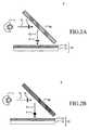
- FIGS. 1A and 1Billustrate the basics of the process described for exposure of an optical film 40 comprising a photosensitive layer 20 and a substrate 10 .
- a light source 1emits a polarized light 91 having p-polarization.
- Transmissive mask 98a transmissive LCD spatial light modulator, selectively modulates exposure beam 92 over each pixel area to provide either p-polarized light, as shown in FIG. 1A, or s-polarized light, as shown in FIG. 1B.
- the solution of U.S. patent application Publication No. 2002-0027624 A1offers a mask solution that is dynamically changeable, eliminating the need to prepare and deploy separate masking components to support optical film fabrication.
- a photo-alignment methodmay be one of three basic types:
- LCPliquid crystal polymer
- LCP materialsinclude cross-linkable liquid crystalline monomers, oligomers, or pre-polymers having cross-linkable groups.
- the cross-linkable liquid crystal materialmay exhibit a nematic, smectic, or cholesteric phase.
- the object of the present inventionis to provide an improved apparatus and method for forming a pattern in fabrication of optical film.
- the present inventionprovides an apparatus for exposing a pattern onto a photosensitive medium, the apparatus comprising:
- a polarization light modulatorcomprising an array of pixels for modulating, at each pixel, the polarization state of the incident light beam
- a feature of the present inventionis the formation of a pattern onto a photosensitive medium by modulating the polarization of a beam of light that is directed toward the photosensitive layer.
- FIGS. 1A and 1Bshow schematics of a prior art exposure apparatus for exposing a pattern onto optical film using a transmissive LCD for modulating polarization state;
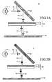
- FIGS. 2A and 2Bshow schematics of an apparatus of the present invention for exposing a pattern onto optical film using a reflective LCD for modulating polarization state;
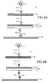
- FIGS. 4A and 4Bshow schematics of an optional embodiment of the present invention using a reflective surface to re-use exposure energy that had been transmitted through the optical film when using a transmissive spatial light modulator.
- the terms “photosensitive” and “photoreactive”are considered to be equivalent.
- the system and method of the present inventionare directed to exposure of photoreactive materials in optical films used for alignment of LCP layers, however, the system and methods disclosed herein can be more broadly applied to fabrication of optical films overall, wherever a layer of photosensitive material is exposed or irradiated to take advantage of a photoreaction as part of optical film manufacture.
- a substrate layermust have sufficient mechanical strength to serve as a support for additional layers.
- a substrateIn roll-to-roll web fabrication, a substrate must have sufficient strength to allow it to be wound or unwound from a roll, for example.
- Typical substrate materials for optical filminclude triacetate cellulose (TAC), polyester, polycarbonate, or other transparent polymers, with thickness typically in the 25 to 500 micrometer range.
- TACtriacetate cellulose
- an orientation layer or anisotropic layer comprising photoreactive materialis typically less than about five micrometers thick and often less than two micrometers thick; such layers cannot be used or considered as a substrate.
- optical filmis fabricated along a web in a roll-to-roll manufacturing process.
- the apparatus and methods of the present inventioncould be generally applied to applications using glass or other rigid material as a substrate.
- exposure irradiationis used to condition photoreactive media for fabrication of an optical film.
- the term “condition,” as used here,must be properly understood.
- exposure energyconditions the optical film by causing an alignment photoreaction.
- Typical alignment photoreactionsinclude isomerization, photo-dimerization, and photo-dissociation, as described in the background section above.
- the method of the present inventioncan be used with other types of conditioning, including curing for example.
- optical materialsmay have up to three different principal indices of refraction and can be classified as either isotropic or anisotropic based on the relationship of these indices. When all three of its principal indices are equal, a material is considered to be isotropic. When anisotropic, a material can be either uniaxial, or biaxial. When two principal indices are equal, a material is considered to be uniaxial.
- An uniaxial materialis uniquely characterized as having an ordinary index, referred as n o , an extraordinary index n e , and two angles describing the orientation of its optical axis, the axis of n e .
- n eWhen n e is greater than n o , an uniaxial material is positively birefringent. When n e is smaller than n o , an uniaxial material is negatively birefringent. Controlling birefringent behavior is particularly useful in the fabrication and application of optical films. When all three refractive indices differ, a material is considered to be biaxial, uniquely specified by its principal indices nx 0 , ny 0 , nz 0 , and three orientational angles.
- FIGS. 2A and 2Bshow an exposure apparatus 8 for fabrication of optical film 40 having a pattern formed by exposure to polarized light.
- a reflective polarization modulation device 88modulates the polarization state of an incident light beam 81 from light source 1 .
- a modulated exposure beam 82is directed to photosensitive layer 20 which is coupled to a substrate 10 .
- Reflective polarization modulation device 88is a reflective LCD spatial light modulator in one embodiment.
- the reflective LCDprovides an array of pixels, each of which can be individually addressed and modulated.
- FIG. 2Ashows the behavior of reflective polarization modulation device 88 for an unmodulated pixel, where the polarization state of the pixel in modulated exposure beam 82 is the same p-polarization state as the state of incident light beam 81 .
- FIG. 2Bshows the modulation of a pixel to an s-polarization state.
- the arrangement of modulated and unmodulated pixels on reflective polarization modulation device 88determines the pattern imposed on photosensitive layer 20 by modulated exposure beam 82 .
- FIGS. 2A and 2Bare only one of the numerous possible angular arrangements for reflective polarization modulation device 88 relative to light source 1 and the surface of optical film 40 .
- exposure beam 82is incident at a normal to optical film 40 .
- the relative angle of reflective polarization modulation device 88can be utilized to provide exposure beam 82 incidence at a suitable angle for the type of optical film 40 being fabricated.
- incident light beam 81 and exposure beam 82may be collimated for some applications; specific types of photosensitive material may exhibit improved response to collimated light.
- exposure apparatus 8can be used with a number of different types of photosensitive layer 20 , depending on the function of optical film 40 .
- Photosensitive layer 20may be sensitive to exposure irradiation from UV light, from visible light, or even from infrared light.
- optical film 40could be stationary, provided as individual sheets, for example. Alternately, optical film 40 could be provided on a web, such as in a roll-to-roll manufacturing operation.
- Optical film 40could have any number of layers, in addition to at least one photosensitive layer 20 .
- Exposure apparatus 8could have applications beyond that of film fabrication; substrate 10 could be glass or other hard material upon which photosensitive layer 20 is treated.
- the pattern imposed on optical film 40could be a static pattern, such as for an alignment film.
- exposure apparatus 8is capable of applying other types of pattern. For example, identity or security images or some other type of patterning can be applied within the scope of the present invention.
- Light source 1provides polarized light and may include an optional filter for providing light having a specific range or ranges of wavelengths.
- exposure apparatus 8includes a reflective surface 50 for re-using a portion of the exposure energy, as disclosed commonly-assigned copending U.S. patent application Ser. No. 10/242,564.
- Reflective surface 50is located opposite reflective polarization modulator 88 with respect to optical film 40 .
- Reflective surface 50reflects a portion of a residual beam 83 back as a reflected beam 84 toward optical film 40 .
- reflected beam 84preserves the polarization state of residual beam 83 , independent of the pixel state at reflective polarization modulator 88 .
- the re-used reflected beam 84could be used to complement the pattern-forming function of reflective polarization modulator 88 by adding to the photoreactive response achieved by exposure beam 82 .
- reflected beam 84could have an opposing effect, mediating the photoreactive response achieved by exposure beam 82 .
- Reflected beam 84could further serve some alternate purpose, such as providing energy for curing, for example.
- reflective surface 50may be a mirror or a retroreflective surface, and may be oriented parallel to the surface of optical film 40 or at some oblique angle relative to that surface. To aid in fabrication of optical film 40 , reflective surface 50 may be coupled to optical film 40 , such as using static attraction or an adhesive for example.
- FIGS. 4A and 4Banother embodiment of the present invention is shown in which an exposure apparatus 9 employs reflective surface 50 in cooperation with a transmissive spatial light modulator as transmissive mask 98 .
- This embodimentalso allows re-use of a portion of the exposure energy, as described above for the reflective embodiment of FIGS. 3A and 3B.
- the embodiment of FIGS. 4A and 4Bhelps to increase the exposure energy available when using a transmissive spatial light modulator, to help compensate for shortcomings of the transmissive mask method, as noted in the background material above.
Landscapes
- Physics & Mathematics (AREA)
- General Physics & Mathematics (AREA)
- Life Sciences & Earth Sciences (AREA)
- Sustainable Development (AREA)
- Exposure And Positioning Against Photoresist Photosensitive Materials (AREA)
- Printers Or Recording Devices Using Electromagnetic And Radiation Means (AREA)
- Facsimile Scanning Arrangements (AREA)
Abstract
Description
- This is a continuation-in-part of application Ser. No. 10/242,048, filed Sep. 12, 2002, entitled APPARATUS AND METHOD FOR SELECTIVELY EXPOSING PHOTOSENSITIVE MATERIALS USING A REFLECTIVE LIGHT MODULATOR, by Xiang-Dong Mi.[0001]
- This invention generally relates to a method and a system for manufacturing an optical film and more particularly relates to a method and system for fabrication of an optical film having a patterned layer formed by exposure of photosensitive material using a spatial light modulator.[0002]
- Considerable interest has been shown in photo-alignment methods for the fabrication of optical components including optical films. As just one example among many, U.S. Pat. No. 6,061,138 (Gibbon et al.) discloses a photo-alignment process using UV light for aligning a liquid crystal medium. Among the advantages of photo-alignment methods over traditional mechanical alignment methods, such as rubbing, is the capability to generate a high resolution pattern in the exposed photosensitive medium. Photo-alignment techniques can be used to form patterned alignment layers such as those used in an liquid crystal display (LCD) to create multi-domain liquid crystal structures and patterned optical films used as image cards, security cards, and the like. Depending upon the response characteristics of the photosensitive medium, patterns can be formed by changing various characteristics of the exposure energy, typically intensity or polarization, for example.[0003]
- In photolithography, used, for example, in the manufacture of electronic circuits on silicon, a geometric pattern is imposed onto a photoresist wafer substrate by applying a mask to selectively block the exposure energy over specific areas. This same concept, using a static mask, can be applied to optical film fabrication, where the same regular pattern is used repeatedly as part of the fabrication process.[0004]
- Driven in part by the high costs and schedule impact of mask fabrication and the difficulty of changing masks to correct for errors or to rework a fabrication process, the semiconductor industry has shown significant interest in “maskless” photolithography. Using this approach, as exemplified in U.S. Pat. No. 5,691,541 (Ceglio et al.) and U.S. Pat. No. 6,060,224 (Sweatt et al.), a digital micromirror device (DMD) is used to reflect a pattern onto the photoresist substrate. The DMD comprises an array of tiny mirrors, each separately addressable for reflecting light onto or away from the photoresist substrate. The exposure pattern can thus be formed on the DMD. Then, the exposure source is reflected from the DMD surface and focused onto the substrate for forming circuitry components. This approach appears to have merit where light intensity is used to form the desired pattern.[0005]
- For many types of optical film, such as the film treated using the apparatus of U.S. Pat. No. 6,061,138, for example, the polarization state and direction of light, rather than light intensity, is used for conditioning alignment or other pattern formation in a photosensitive medium. Following the photolithography paradigm, masks have been employed in a number of devices used for exposure of optical film with polarized light, as is disclosed in U.S. Pat. No. 5,389,698 (Chigrinov et al.) It can be expected, however, that some of the same cost and deployment difficulties confronted when using masks in microlithography will also discourage the use of masks with optical film fabrication.[0006]
- In an attempt to meet the need for an adaptive solution, U.S. patent application Publication No. 2002/0027624 A1 (Seiberle) discloses a transmissive optical component that acts as a mask, producing patterned, linearly polarized light. FIGS. 1A and 1B illustrate the basics of the process described for exposure of an[0007]
optical film 40 comprising aphotosensitive layer 20 and asubstrate 10. Alight source 1 emits a polarizedlight 91 having p-polarization.Transmissive mask 98, a transmissive LCD spatial light modulator, selectively modulatesexposure beam 92 over each pixel area to provide either p-polarized light, as shown in FIG. 1A, or s-polarized light, as shown in FIG. 1B. As with the DMD solution for microlithography described above, the solution of U.S. patent application Publication No. 2002-0027624 A1 offers a mask solution that is dynamically changeable, eliminating the need to prepare and deploy separate masking components to support optical film fabrication. - When used for photo-alignment,[0008]
photosensitive layer 20 is typically a thin photo-reactive alignment medium, typically linear photo-polymerization media (LPP), also known as photo-oriented polymer network (PPN).Photosensitive layer 20 is applied tosubstrate 10 and is then irradiated, typically using UV light, to provide a directional alignment bias. - There are a number of photo-alignment methods, based on different photoreaction processes. In general, a photo-alignment method may be one of three basic types:[0009]
- (1) Isomerization, as disclosed in U.S. Pat. No. 4,974,941 (Gibbons et al.);[0010]
- (2) Photo-dimerization, as disclosed in U.S. Pat. No. 5,602,661 (Schadt et al.); and[0011]
- (3) Photo-dissociation, as taught in “Prospects of the photo-alignment technique for LCD fabrication” SID Digest 1997, pp. 311-314 (Iimura et al.).[0012]
- Once[0013]
photosensitive layer 20 is aligned, a liquid crystal polymer (LCP) layer is applied over the LPP layer that has been treated to provide a preferred alignment orientation. As is well known in the photoaligment art, LCP materials include cross-linkable liquid crystalline monomers, oligomers, or pre-polymers having cross-linkable groups. Depending on the intended application, the cross-linkable liquid crystal material may exhibit a nematic, smectic, or cholesteric phase. - Although transmissive LCD spatial light modulators have been used successfully in a number of projection display apparatus, these devices have inherent disadvantages for high-energy exposure environments. As is well-known in the optical arts, transmissive LCDs are fabricated onto a clear substrate, so that circuit traces and componentry reduce the active area of each LCD cell that modulates a pixel. As a result, the effective aperture size for each pixel is a fraction of the area available on the transmissive LCD. This is a significant constraint on the amount of light available for each pixel, whether considered in terms of brightness, irradiance, or exposure energy. As a result, higher energy light sources must be used, with low levels of efficiency. Due to device geometry, there are also limitations to the resolution levels that can be achieved. Thus, while the transmissive LCD of U.S. patent application Publication No. 2002/0027624 has some capability for adaptive pattern forming on optical film, there are inherent limitations with respect to allowable intensity and resolution. Imaging at other than 1:1 magnification presents further difficulties, due to interference effects and focus restrictions.[0014]
- Reflective LCD spatial light modulators have been used to modulate the polarization of incident light in imaging apparatus for display and projection. In these devices, light directed to the reflective LCD via a polarization beamsplitter is modulated by selectively altering the polarization state of individual pixels of incident light. The reflected light is sent back in the same direction as the incident light, but is transmitted through the polarization beamsplitter along its way to a display surface. For example, LCD spatial light modulators have been developed and employed for digital projection systems for image display, such as is disclosed in U.S. Pat. No. 5,325,137 (Konno et al.) and in miniaturized image display apparatus suitable for mounting within a helmet or supported by eyeglasses, as is disclosed in U.S. Pat. No. 5,808,800 (Handschy et al.) Improvements in reflective LCD components have improved the resolution of these devices. Because each pixel cell in the LCD array is reflective, aperture sizes are maximized, providing significant improvements in brightness or irradiance when compared with transmissive LCDs. However, disclosed uses of reflective LCD components are in image-forming for print and projection apparatus.[0015]
- Thus, it can be seen that, while there have been some solutions presented for fabricating a patterned optical film by exposure of photosensitive materials using masks, there is room for improvement, particularly with respect to light efficiency and resolution.[0016]
- The object of the present invention is to provide an improved apparatus and method for forming a pattern in fabrication of optical film. With this object in mind, the present invention provides an apparatus for exposing a pattern onto a photosensitive medium, the apparatus comprising:[0017]
- (a) a source of exposure radiation for providing an incident light beam to a polarization light modulator;[0018]
- (b) a polarization light modulator comprising an array of pixels for modulating, at each pixel, the polarization state of the incident light beam;[0019]
- (c) a reflective surface disposed to reflect, back through the photosensitive medium, a portion of the exposure beam transmitted through the photosensitive medium, in order to obtain a photoreactive response thereby; and[0020]
- wherein the source of exposure radiation and the reflective surface are on opposite sides of the photosensitive medium.[0021]
- A feature of the present invention is the formation of a pattern onto a photosensitive medium by modulating the polarization of a beam of light that is directed toward the photosensitive layer.[0022]
- It is an advantage of the present invention that, because it uses an LCD spatial light modulator as a “mask,” it allows a pattern to be changed quickly, even during exposure operation.[0023]
- It is a further advantage of the present invention that it employs reflective means for supplementing the radiant energy available from modulated light.[0024]
- These and other objects, features, and advantages of the present invention will become apparent to those skilled in the art upon a reading of the following detailed description when taken in conjunction with the drawings wherein there is shown and described an illustrative embodiment of the invention.[0025]
- While the specification concludes with claims particularly pointing out and distinctly claiming the subject matter of the present invention, it is believed that the invention will be better understood from the following description when taken in conjunction with the accompanying drawings, wherein:[0026]
- FIGS. 1A and 1B show schematics of a prior art exposure apparatus for exposing a pattern onto optical film using a transmissive LCD for modulating polarization state;[0027]
- FIGS. 2A and 2B show schematics of an apparatus of the present invention for exposing a pattern onto optical film using a reflective LCD for modulating polarization state;[0028]
- FIGS. 3A and 3B show schematics of an optional embodiment of the present invention using a reflective surface to re-use exposure energy that had been transmitted through the optical film when using a reflective spatial light modulator; and[0029]
- FIGS. 4A and 4B show schematics of an optional embodiment of the present invention using a reflective surface to re-use exposure energy that had been transmitted through the optical film when using a transmissive spatial light modulator.[0030]
- The present description is directed in particular to elements forming part of, or cooperating more directly with, apparatus in accordance with the invention. It is to be understood that elements not specifically shown or described may take various forms well known to those skilled in the art.[0031]
- For the purposes of this application, the terms “photosensitive” and “photoreactive” are considered to be equivalent. In a preferred embodiment, the system and method of the present invention are directed to exposure of photoreactive materials in optical films used for alignment of LCP layers, however, the system and methods disclosed herein can be more broadly applied to fabrication of optical films overall, wherever a layer of photosensitive material is exposed or irradiated to take advantage of a photoreaction as part of optical film manufacture.[0032]
- With respect to optical films, a substrate layer must have sufficient mechanical strength to serve as a support for additional layers. In roll-to-roll web fabrication, a substrate must have sufficient strength to allow it to be wound or unwound from a roll, for example. Typical substrate materials for optical film include triacetate cellulose (TAC), polyester, polycarbonate, or other transparent polymers, with thickness typically in the 25 to 500 micrometer range. By comparison, an orientation layer or anisotropic layer comprising photoreactive material is typically less than about five micrometers thick and often less than two micrometers thick; such layers cannot be used or considered as a substrate. For the preferred embodiment, optical film is fabricated along a web in a roll-to-roll manufacturing process. However, the apparatus and methods of the present invention could be generally applied to applications using glass or other rigid material as a substrate.[0033]
- In the apparatus and method of the present invention, exposure irradiation is used to condition photoreactive media for fabrication of an optical film. The term “condition,” as used here, must be properly understood. In the preferred embodiment, exposure energy conditions the optical film by causing an alignment photoreaction. Typical alignment photoreactions include isomerization, photo-dimerization, and photo-dissociation, as described in the background section above. However, the method of the present invention can be used with other types of conditioning, including curing for example.[0034]
- As is well known in the art, optical materials may have up to three different principal indices of refraction and can be classified as either isotropic or anisotropic based on the relationship of these indices. When all three of its principal indices are equal, a material is considered to be isotropic. When anisotropic, a material can be either uniaxial, or biaxial. When two principal indices are equal, a material is considered to be uniaxial. An uniaxial material is uniquely characterized as having an ordinary index, referred as n[0035]o, an extraordinary index ne, and two angles describing the orientation of its optical axis, the axis of ne. When neis greater than no, an uniaxial material is positively birefringent. When neis smaller than no, an uniaxial material is negatively birefringent. Controlling birefringent behavior is particularly useful in the fabrication and application of optical films. When all three refractive indices differ, a material is considered to be biaxial, uniquely specified by its principal indices nx0, ny0, nz0, and three orientational angles.
- FIGS. 2A and 2B show an[0036]
exposure apparatus 8 for fabrication ofoptical film 40 having a pattern formed by exposure to polarized light. A reflectivepolarization modulation device 88 modulates the polarization state of anincident light beam 81 fromlight source 1. A modulatedexposure beam 82 is directed tophotosensitive layer 20 which is coupled to asubstrate 10. - Reflective[0037]
polarization modulation device 88 is a reflective LCD spatial light modulator in one embodiment. The reflective LCD provides an array of pixels, each of which can be individually addressed and modulated. FIG. 2A shows the behavior of reflectivepolarization modulation device 88 for an unmodulated pixel, where the polarization state of the pixel in modulatedexposure beam 82 is the same p-polarization state as the state ofincident light beam 81. FIG. 2B shows the modulation of a pixel to an s-polarization state. The arrangement of modulated and unmodulated pixels on reflectivepolarization modulation device 88 determines the pattern imposed onphotosensitive layer 20 by modulatedexposure beam 82. - It must be observed that the diagonal positioning of FIGS. 2A and 2B is only one of the numerous possible angular arrangements for reflective[0038]
polarization modulation device 88 relative tolight source 1 and the surface ofoptical film 40. With the arrangement of FIGS. 2A and 2B,exposure beam 82 is incident at a normal tooptical film 40. For some types ofphotosensitive layer 20, including many types of alignment media, oblique incidence is desirable. Thus, the relative angle of reflectivepolarization modulation device 88 can be utilized to provideexposure beam 82 incidence at a suitable angle for the type ofoptical film 40 being fabricated. It must also be noted thatincident light beam 81 andexposure beam 82 may be collimated for some applications; specific types of photosensitive material may exhibit improved response to collimated light. - It should be understood that[0039]
exposure apparatus 8 can be used with a number of different types ofphotosensitive layer 20, depending on the function ofoptical film 40.Photosensitive layer 20 may be sensitive to exposure irradiation from UV light, from visible light, or even from infrared light. During exposure,optical film 40 could be stationary, provided as individual sheets, for example. Alternately,optical film 40 could be provided on a web, such as in a roll-to-roll manufacturing operation.Optical film 40 could have any number of layers, in addition to at least onephotosensitive layer 20. Clearly, best results and maximum efficiency are obtained whenexposure apparatus 8 is suitably matched to the sensitivity characteristics ofphotosensitive layer 20 inoptical film 40.Exposure apparatus 8 could have applications beyond that of film fabrication;substrate 10 could be glass or other hard material upon whichphotosensitive layer 20 is treated. - The pattern imposed on[0040]
optical film 40 could be a static pattern, such as for an alignment film. However,exposure apparatus 8 is capable of applying other types of pattern. For example, identity or security images or some other type of patterning can be applied within the scope of the present invention. - [0041]
Light source 1 provides polarized light and may include an optional filter for providing light having a specific range or ranges of wavelengths. - Referring to FIGS. 3A and 3B, an embodiment of the present invention is shown in which[0042]
exposure apparatus 8 includes areflective surface 50 for re-using a portion of the exposure energy, as disclosed commonly-assigned copending U.S. patent application Ser. No. 10/242,564.Reflective surface 50 is located oppositereflective polarization modulator 88 with respect tooptical film 40.Reflective surface 50 reflects a portion of aresidual beam 83 back as a reflectedbeam 84 towardoptical film 40. As is represented in FIGS. 3A and 3B, reflectedbeam 84 preserves the polarization state ofresidual beam 83, independent of the pixel state atreflective polarization modulator 88. By re-using exposure energy that would otherwise be wasted, the arrangement of FIGS. 3A and 3B can help to increase the overall efficiency ofexposure apparatus 8. The re-used reflectedbeam 84 could be used to complement the pattern-forming function ofreflective polarization modulator 88 by adding to the photoreactive response achieved byexposure beam 82. Alternately, reflectedbeam 84 could have an opposing effect, mediating the photoreactive response achieved byexposure beam 82.Reflected beam 84 could further serve some alternate purpose, such as providing energy for curing, for example. As is noted in commonly-assigned copending U.S. patent application Ser. No. 10/242,564,reflective surface 50 may be a mirror or a retroreflective surface, and may be oriented parallel to the surface ofoptical film 40 or at some oblique angle relative to that surface. To aid in fabrication ofoptical film 40,reflective surface 50 may be coupled tooptical film 40, such as using static attraction or an adhesive for example. - Referring to FIGS. 4A and 4B, another embodiment of the present invention is shown in which an[0043]
exposure apparatus 9 employsreflective surface 50 in cooperation with a transmissive spatial light modulator astransmissive mask 98. This embodiment also allows re-use of a portion of the exposure energy, as described above for the reflective embodiment of FIGS. 3A and 3B. The embodiment of FIGS. 4A and 4B helps to increase the exposure energy available when using a transmissive spatial light modulator, to help compensate for shortcomings of the transmissive mask method, as noted in the background material above. - The invention has been described in detail with particular reference to certain preferred embodiments thereof, but it will be understood that variations and modifications can be effected within the scope of the invention. Therefore, what is provided is an improved apparatus and method for forming a pattern in fabrication of optical film using a spatial light modulator.[0044]
- [0045]1 Light source
- [0046]8 Exposure apparatus
- [0047]9 Exposure apparatus
- [0048]10 Substrate
- [0049]20 Photosensitive layer
- [0050]40 Optical film
- [0051]50 Reflective surface
- [0052]81 Incident light beam
- [0053]82 Exposure beam
- [0054]83 Residual beam
- [0055]84 Reflected beam
- [0056]88 Reflective polarization modulation device
- [0057]91 Polarized light
- [0058]92 Exposure beam
- [0059]98 Transmissive mask
Claims (21)
Priority Applications (1)
| Application Number | Priority Date | Filing Date | Title |
|---|---|---|---|
| US10/760,812US6914708B2 (en) | 2002-09-12 | 2004-01-20 | Apparatus and method for selectively exposing photosensitive materials using a spatial light modulator |
Applications Claiming Priority (2)
| Application Number | Priority Date | Filing Date | Title |
|---|---|---|---|
| US10/242,048US6751003B2 (en) | 2002-09-12 | 2002-09-12 | Apparatus and method for selectively exposing photosensitive materials using a reflective light modulator |
| US10/760,812US6914708B2 (en) | 2002-09-12 | 2004-01-20 | Apparatus and method for selectively exposing photosensitive materials using a spatial light modulator |
Related Parent Applications (1)
| Application Number | Title | Priority Date | Filing Date |
|---|---|---|---|
| US10/242,048Continuation-In-PartUS6751003B2 (en) | 2002-09-12 | 2002-09-12 | Apparatus and method for selectively exposing photosensitive materials using a reflective light modulator |
Publications (2)
| Publication Number | Publication Date |
|---|---|
| US20040145794A1true US20040145794A1 (en) | 2004-07-29 |
| US6914708B2 US6914708B2 (en) | 2005-07-05 |
Family
ID=31991312
Family Applications (2)
| Application Number | Title | Priority Date | Filing Date |
|---|---|---|---|
| US10/242,048Expired - LifetimeUS6751003B2 (en) | 2002-09-12 | 2002-09-12 | Apparatus and method for selectively exposing photosensitive materials using a reflective light modulator |
| US10/760,812Expired - LifetimeUS6914708B2 (en) | 2002-09-12 | 2004-01-20 | Apparatus and method for selectively exposing photosensitive materials using a spatial light modulator |
Family Applications Before (1)
| Application Number | Title | Priority Date | Filing Date |
|---|---|---|---|
| US10/242,048Expired - LifetimeUS6751003B2 (en) | 2002-09-12 | 2002-09-12 | Apparatus and method for selectively exposing photosensitive materials using a reflective light modulator |
Country Status (3)
| Country | Link |
|---|---|
| US (2) | US6751003B2 (en) |
| JP (1) | JP2004102262A (en) |
| TW (1) | TW200415253A (en) |
Cited By (4)
| Publication number | Priority date | Publication date | Assignee | Title |
|---|---|---|---|---|
| CN106680216A (en)* | 2016-12-06 | 2017-05-17 | 天津津航技术物理研究所 | Method for calculating reflectivity and transmissivity spectrums of binary laminated optical material |
| CN107741672A (en)* | 2017-10-25 | 2018-02-27 | 深圳市华星光电技术有限公司 | A kind of platform applied to MMG panels and the method to MMG panel orientations |
| CN108957863A (en)* | 2018-06-29 | 2018-12-07 | 武汉华星光电技术有限公司 | A kind of smooth orientation equipment |
| CN112817179A (en)* | 2019-11-15 | 2021-05-18 | 苏州大学 | Patterned liquid crystal photo-alignment device with phase compensation function and method |
Families Citing this family (36)
| Publication number | Priority date | Publication date | Assignee | Title |
|---|---|---|---|---|
| US6909473B2 (en)* | 2002-01-07 | 2005-06-21 | Eastman Kodak Company | Display apparatus and method |
| US7061561B2 (en)* | 2002-01-07 | 2006-06-13 | Moxtek, Inc. | System for creating a patterned polarization compensator |
| CN100365451C (en)* | 2002-07-30 | 2008-01-30 | 日东电工株式会社 | Optical film and method for producing same |
| US6943930B2 (en)* | 2002-09-12 | 2005-09-13 | Eastman Kodak Company | Method and system for fabricating optical film using an exposure source and reflecting surface |
| US6751003B2 (en)* | 2002-09-12 | 2004-06-15 | Eastman Kodak Company | Apparatus and method for selectively exposing photosensitive materials using a reflective light modulator |
| DE10338983A1 (en)* | 2003-08-20 | 2005-03-17 | Carl Zeiss Smt Ag | Projection lens for microlithography scans a pattern set up in a projection lens object plane into a projection lens focal plane |
| JP2005091480A (en)* | 2003-09-12 | 2005-04-07 | Nitto Denko Corp | Method for producing anisotropic film |
| US20080055720A1 (en)* | 2006-08-31 | 2008-03-06 | Perkins Raymond T | Optical Data Storage System with an Inorganic, Dielectric Grid Polarizer |
| US20080055721A1 (en)* | 2006-08-31 | 2008-03-06 | Perkins Raymond T | Light Recycling System with an Inorganic, Dielectric Grid Polarizer |
| US7800823B2 (en)* | 2004-12-06 | 2010-09-21 | Moxtek, Inc. | Polarization device to polarize and further control light |
| US7961393B2 (en)* | 2004-12-06 | 2011-06-14 | Moxtek, Inc. | Selectively absorptive wire-grid polarizer |
| US7570424B2 (en)* | 2004-12-06 | 2009-08-04 | Moxtek, Inc. | Multilayer wire-grid polarizer |
| US20080055722A1 (en)* | 2006-08-31 | 2008-03-06 | Perkins Raymond T | Optical Polarization Beam Combiner/Splitter with an Inorganic, Dielectric Grid Polarizer |
| US20080055549A1 (en)* | 2006-08-31 | 2008-03-06 | Perkins Raymond T | Projection Display with an Inorganic, Dielectric Grid Polarizer |
| US7630133B2 (en)* | 2004-12-06 | 2009-12-08 | Moxtek, Inc. | Inorganic, dielectric, grid polarizer and non-zero order diffraction grating |
| US8072552B2 (en)* | 2005-08-19 | 2011-12-06 | Reald Inc. | Stereoscopic eyewear |
| US20070297052A1 (en)* | 2006-06-26 | 2007-12-27 | Bin Wang | Cube wire-grid polarizing beam splitter |
| US20070296921A1 (en)* | 2006-06-26 | 2007-12-27 | Bin Wang | Projection display with a cube wire-grid polarizing beam splitter |
| US8755113B2 (en)* | 2006-08-31 | 2014-06-17 | Moxtek, Inc. | Durable, inorganic, absorptive, ultra-violet, grid polarizer |
| US7789515B2 (en)* | 2007-05-17 | 2010-09-07 | Moxtek, Inc. | Projection device with a folded optical path and wire-grid polarizer |
| US20080316599A1 (en)* | 2007-06-22 | 2008-12-25 | Bin Wang | Reflection-Repressed Wire-Grid Polarizer |
| US9561622B2 (en) | 2008-05-05 | 2017-02-07 | Georgia Tech Research Corporation | Systems and methods for fabricating three-dimensional objects |
| US8636496B2 (en)* | 2008-05-05 | 2014-01-28 | Georgia Tech Research Corporation | Systems and methods for fabricating three-dimensional objects |
| KR100911459B1 (en)* | 2008-08-06 | 2009-08-11 | 삼성전자주식회사 | Alignment film forming method, manufacturing method of liquid crystal display device and alignment film forming device using same |
| US20100103517A1 (en)* | 2008-10-29 | 2010-04-29 | Mark Alan Davis | Segmented film deposition |
| US8248696B2 (en) | 2009-06-25 | 2012-08-21 | Moxtek, Inc. | Nano fractal diffuser |
| US8913321B2 (en) | 2010-09-21 | 2014-12-16 | Moxtek, Inc. | Fine pitch grid polarizer |
| US8611007B2 (en) | 2010-09-21 | 2013-12-17 | Moxtek, Inc. | Fine pitch wire grid polarizer |
| US8873144B2 (en) | 2011-05-17 | 2014-10-28 | Moxtek, Inc. | Wire grid polarizer with multiple functionality sections |
| US8913320B2 (en) | 2011-05-17 | 2014-12-16 | Moxtek, Inc. | Wire grid polarizer with bordered sections |
| US8922890B2 (en) | 2012-03-21 | 2014-12-30 | Moxtek, Inc. | Polarizer edge rib modification |
| EP2856223B1 (en)* | 2012-05-30 | 2020-12-23 | ROLIC Technologies AG | Fast generation of elements with individually patterned anisotropy |
| CN102778820A (en)* | 2012-08-17 | 2012-11-14 | 杭州士兰明芯科技有限公司 | Maskless graphic exposure system based on spatial light modulator |
| US9354374B2 (en) | 2013-10-24 | 2016-05-31 | Moxtek, Inc. | Polarizer with wire pair over rib |
| CN108345180B (en)* | 2017-01-25 | 2020-04-10 | 上海微电子装备(集团)股份有限公司 | Exposure and photo-alignment integrated device and using method thereof |
| CN116520612B (en)* | 2023-04-20 | 2024-05-28 | 成都瑞波科材料科技有限公司 | Optical module and optical film processing apparatus |
Citations (10)
| Publication number | Priority date | Publication date | Assignee | Title |
|---|---|---|---|---|
| US4974941A (en)* | 1989-03-08 | 1990-12-04 | Hercules Incorporated | Process of aligning and realigning liquid crystal media |
| US5325137A (en)* | 1991-08-28 | 1994-06-28 | Victor Company Of Japan, Ltd. | Overhead projector with a spatial light modulator |
| US5389698A (en)* | 1991-07-26 | 1995-02-14 | Hoffmann-La Roche Inc. | Process for making photopolymers having varying molecular orientation using light to orient and polymerize |
| US5602661A (en)* | 1993-02-17 | 1997-02-11 | Hoffmann-La Roche Inc. | Optical component |
| US5691541A (en)* | 1996-05-14 | 1997-11-25 | The Regents Of The University Of California | Maskless, reticle-free, lithography |
| US5808800A (en)* | 1994-12-22 | 1998-09-15 | Displaytech, Inc. | Optics arrangements including light source arrangements for an active matrix liquid crystal image generator |
| US6061138A (en)* | 1997-08-05 | 2000-05-09 | Elsicon, Inc. | Optical exposure systems and processes for alignment of liquid crystals |
| US6060224A (en)* | 1996-06-19 | 2000-05-09 | Sweatt; William C. | Method for maskless lithography |
| US20020027624A1 (en)* | 1995-07-11 | 2002-03-07 | Rolic Ag | Optical component for producing linearly polarized light |
| US6751003B2 (en)* | 2002-09-12 | 2004-06-15 | Eastman Kodak Company | Apparatus and method for selectively exposing photosensitive materials using a reflective light modulator |
Family Cites Families (1)
| Publication number | Priority date | Publication date | Assignee | Title |
|---|---|---|---|---|
| US5488494A (en)* | 1993-10-07 | 1996-01-30 | Tamarack Storage Devices | Packaging system for holographic storage media |
- 2002
- 2002-09-12USUS10/242,048patent/US6751003B2/ennot_activeExpired - Lifetime
- 2003
- 2003-07-22TWTW092119990Apatent/TW200415253A/enunknown
- 2003-08-14JPJP2003293481Apatent/JP2004102262A/enactivePending
- 2004
- 2004-01-20USUS10/760,812patent/US6914708B2/ennot_activeExpired - Lifetime
Patent Citations (10)
| Publication number | Priority date | Publication date | Assignee | Title |
|---|---|---|---|---|
| US4974941A (en)* | 1989-03-08 | 1990-12-04 | Hercules Incorporated | Process of aligning and realigning liquid crystal media |
| US5389698A (en)* | 1991-07-26 | 1995-02-14 | Hoffmann-La Roche Inc. | Process for making photopolymers having varying molecular orientation using light to orient and polymerize |
| US5325137A (en)* | 1991-08-28 | 1994-06-28 | Victor Company Of Japan, Ltd. | Overhead projector with a spatial light modulator |
| US5602661A (en)* | 1993-02-17 | 1997-02-11 | Hoffmann-La Roche Inc. | Optical component |
| US5808800A (en)* | 1994-12-22 | 1998-09-15 | Displaytech, Inc. | Optics arrangements including light source arrangements for an active matrix liquid crystal image generator |
| US20020027624A1 (en)* | 1995-07-11 | 2002-03-07 | Rolic Ag | Optical component for producing linearly polarized light |
| US5691541A (en)* | 1996-05-14 | 1997-11-25 | The Regents Of The University Of California | Maskless, reticle-free, lithography |
| US6060224A (en)* | 1996-06-19 | 2000-05-09 | Sweatt; William C. | Method for maskless lithography |
| US6061138A (en)* | 1997-08-05 | 2000-05-09 | Elsicon, Inc. | Optical exposure systems and processes for alignment of liquid crystals |
| US6751003B2 (en)* | 2002-09-12 | 2004-06-15 | Eastman Kodak Company | Apparatus and method for selectively exposing photosensitive materials using a reflective light modulator |
Cited By (4)
| Publication number | Priority date | Publication date | Assignee | Title |
|---|---|---|---|---|
| CN106680216A (en)* | 2016-12-06 | 2017-05-17 | 天津津航技术物理研究所 | Method for calculating reflectivity and transmissivity spectrums of binary laminated optical material |
| CN107741672A (en)* | 2017-10-25 | 2018-02-27 | 深圳市华星光电技术有限公司 | A kind of platform applied to MMG panels and the method to MMG panel orientations |
| CN108957863A (en)* | 2018-06-29 | 2018-12-07 | 武汉华星光电技术有限公司 | A kind of smooth orientation equipment |
| CN112817179A (en)* | 2019-11-15 | 2021-05-18 | 苏州大学 | Patterned liquid crystal photo-alignment device with phase compensation function and method |
Also Published As
| Publication number | Publication date |
|---|---|
| US6914708B2 (en) | 2005-07-05 |
| US6751003B2 (en) | 2004-06-15 |
| TW200415253A (en) | 2004-08-16 |
| US20040051928A1 (en) | 2004-03-18 |
| JP2004102262A (en) | 2004-04-02 |
Similar Documents
| Publication | Publication Date | Title |
|---|---|---|
| US6914708B2 (en) | Apparatus and method for selectively exposing photosensitive materials using a spatial light modulator | |
| US10031424B2 (en) | Fabrication of high efficiency, high quality, large area diffractive waveplates and arrays | |
| JP3362814B2 (en) | Switchable holographic device | |
| US11003028B2 (en) | Photo-alignment apparatus that realizes desirable distribution through single exposure and method of manufacturing an optical element | |
| JP3881865B2 (en) | Optical recording apparatus and method, and exposure apparatus and method | |
| US7548301B2 (en) | Maskless optical writer | |
| JP4023541B2 (en) | Lithographic projection apparatus and device manufacturing method | |
| CN101995598B (en) | There is the liquid crystal layer at the inclination angle spatially changed | |
| JP2001194626A (en) | Optical device | |
| US6943930B2 (en) | Method and system for fabricating optical film using an exposure source and reflecting surface | |
| JP3502930B2 (en) | Optical alignment device | |
| EP0701149B1 (en) | Polarisation dependent refractive device and methods of manufacture thereof | |
| JP3649824B2 (en) | Method for manufacturing liquid crystal display device and apparatus for manufacturing the same | |
| KR20040100869A (en) | Irradiation apparatus of polarization light for light orientation | |
| JPH11119439A (en) | LCD mask type exposure marking system | |
| EP1439425A1 (en) | Lithographic projection apparatus and device manufacturing method | |
| JP2000221465A (en) | Method for manufacturing diffractive optical element | |
| KR960039114A (en) | Mask using polarized material and manufacturing method thereof | |
| HK1155521B (en) | Lc layers having a spatially-varying tilt angle |
Legal Events
| Date | Code | Title | Description |
|---|---|---|---|
| AS | Assignment | Owner name:EASTMAN KODAK COMPANY, NEW YORK Free format text:ASSIGNMENT OF ASSIGNORS INTEREST;ASSIGNOR:MI, XIANG-DONG;REEL/FRAME:014915/0011 Effective date:20040119 | |
| FEPP | Fee payment procedure | Free format text:PAYOR NUMBER ASSIGNED (ORIGINAL EVENT CODE: ASPN); ENTITY STATUS OF PATENT OWNER: LARGE ENTITY | |
| STCF | Information on status: patent grant | Free format text:PATENTED CASE | |
| AS | Assignment | Owner name:NITTO DENKO CORPORATION,JAPAN Free format text:ASSIGNMENT OF ASSIGNORS INTEREST;ASSIGNOR:EASTMAN KODAK COMPANY;REEL/FRAME:018816/0960 Effective date:20061219 Owner name:NITTO DENKO CORPORATION, JAPAN Free format text:ASSIGNMENT OF ASSIGNORS INTEREST;ASSIGNOR:EASTMAN KODAK COMPANY;REEL/FRAME:018816/0960 Effective date:20061219 | |
| FPAY | Fee payment | Year of fee payment:4 | |
| FEPP | Fee payment procedure | Free format text:PAYER NUMBER DE-ASSIGNED (ORIGINAL EVENT CODE: RMPN); ENTITY STATUS OF PATENT OWNER: LARGE ENTITY Free format text:PAYOR NUMBER ASSIGNED (ORIGINAL EVENT CODE: ASPN); ENTITY STATUS OF PATENT OWNER: LARGE ENTITY | |
| FPAY | Fee payment | Year of fee payment:8 | |
| FPAY | Fee payment | Year of fee payment:12 |