US20040145019A1 - Strained channel finfet - Google Patents
Strained channel finfetDownload PDFInfo
- Publication number
- US20040145019A1 US20040145019A1US10/349,042US34904203AUS2004145019A1US 20040145019 A1US20040145019 A1US 20040145019A1US 34904203 AUS34904203 AUS 34904203AUS 2004145019 A1US2004145019 A1US 2004145019A1
- Authority
- US
- United States
- Prior art keywords
- crystalline material
- layer
- fin
- lattice constant
- semiconductor device
- Prior art date
- Legal status (The legal status is an assumption and is not a legal conclusion. Google has not performed a legal analysis and makes no representation as to the accuracy of the status listed.)
- Granted
Links
- 239000002178crystalline materialSubstances0.000claimsabstractdescription63
- 239000004065semiconductorSubstances0.000claimsabstractdescription14
- 238000000034methodMethods0.000claimsdescription24
- 229910052710siliconInorganic materials0.000claimsdescription11
- 239000010703siliconSubstances0.000claimsdescription11
- 229910021420polycrystalline siliconInorganic materials0.000claimsdescription5
- 229920005591polysiliconPolymers0.000claimsdescription5
- 230000008569processEffects0.000description9
- 239000012212insulatorSubstances0.000description8
- 239000000758substrateSubstances0.000description8
- XUIMIQQOPSSXEZ-UHFFFAOYSA-NSiliconChemical compound[Si]XUIMIQQOPSSXEZ-UHFFFAOYSA-N0.000description6
- 230000015572biosynthetic processEffects0.000description4
- 238000000151depositionMethods0.000description3
- 238000005530etchingMethods0.000description3
- 239000000463materialSubstances0.000description3
- VYPSYNLAJGMNEJ-UHFFFAOYSA-NSilicium dioxideChemical compoundO=[Si]=OVYPSYNLAJGMNEJ-UHFFFAOYSA-N0.000description2
- BOTDANWDWHJENH-UHFFFAOYSA-NTetraethyl orthosilicateChemical compoundCCO[Si](OCC)(OCC)OCCBOTDANWDWHJENH-UHFFFAOYSA-N0.000description2
- MCMNRKCIXSYSNV-UHFFFAOYSA-NZirconium dioxideChemical compoundO=[Zr]=OMCMNRKCIXSYSNV-UHFFFAOYSA-N0.000description2
- 230000008021depositionEffects0.000description2
- 239000003989dielectric materialSubstances0.000description2
- 239000011810insulating materialSubstances0.000description2
- 238000012986modificationMethods0.000description2
- 230000004048modificationEffects0.000description2
- 101100269850Caenorhabditis elegans mask-1 geneProteins0.000description1
- 229910004541SiNInorganic materials0.000description1
- PNEYBMLMFCGWSK-UHFFFAOYSA-Naluminium oxideInorganic materials[O-2].[O-2].[O-2].[Al+3].[Al+3]PNEYBMLMFCGWSK-UHFFFAOYSA-N0.000description1
- 229910052681coesiteInorganic materials0.000description1
- 229910052593corundumInorganic materials0.000description1
- 229910052906cristobaliteInorganic materials0.000description1
- 238000005137deposition processMethods0.000description1
- 230000000694effectsEffects0.000description1
- 230000005669field effectEffects0.000description1
- 230000006698inductionEffects0.000description1
- 229910001635magnesium fluorideInorganic materials0.000description1
- 238000004519manufacturing processMethods0.000description1
- 150000004767nitridesChemical class0.000description1
- 238000012856packingMethods0.000description1
- 238000000059patterningMethods0.000description1
- 238000005498polishingMethods0.000description1
- 230000009467reductionEffects0.000description1
- 239000000377silicon dioxideSubstances0.000description1
- LIVNPJMFVYWSIS-UHFFFAOYSA-Nsilicon monoxideInorganic materials[Si-]#[O+]LIVNPJMFVYWSIS-UHFFFAOYSA-N0.000description1
- 229910052814silicon oxideInorganic materials0.000description1
- 229910052682stishoviteInorganic materials0.000description1
- -1structuresSubstances0.000description1
- 239000000126substanceSubstances0.000description1
- 229910052905tridymiteInorganic materials0.000description1
- 229910001845yogo sapphireInorganic materials0.000description1
Images


Classifications
- H—ELECTRICITY
- H10—SEMICONDUCTOR DEVICES; ELECTRIC SOLID-STATE DEVICES NOT OTHERWISE PROVIDED FOR
- H10D—INORGANIC ELECTRIC SEMICONDUCTOR DEVICES
- H10D30/00—Field-effect transistors [FET]
- H10D30/60—Insulated-gate field-effect transistors [IGFET]
- H10D30/62—Fin field-effect transistors [FinFET]
- H—ELECTRICITY
- H10—SEMICONDUCTOR DEVICES; ELECTRIC SOLID-STATE DEVICES NOT OTHERWISE PROVIDED FOR
- H10D—INORGANIC ELECTRIC SEMICONDUCTOR DEVICES
- H10D30/00—Field-effect transistors [FET]
- H10D30/01—Manufacture or treatment
- H10D30/021—Manufacture or treatment of FETs having insulated gates [IGFET]
- H10D30/024—Manufacture or treatment of FETs having insulated gates [IGFET] of fin field-effect transistors [FinFET]
- H—ELECTRICITY
- H10—SEMICONDUCTOR DEVICES; ELECTRIC SOLID-STATE DEVICES NOT OTHERWISE PROVIDED FOR
- H10D—INORGANIC ELECTRIC SEMICONDUCTOR DEVICES
- H10D30/00—Field-effect transistors [FET]
- H10D30/60—Insulated-gate field-effect transistors [IGFET]
- H10D30/67—Thin-film transistors [TFT]
- H10D30/6729—Thin-film transistors [TFT] characterised by the electrodes
- H10D30/6737—Thin-film transistors [TFT] characterised by the electrodes characterised by the electrode materials
- H10D30/6739—Conductor-insulator-semiconductor electrodes
- H—ELECTRICITY
- H10—SEMICONDUCTOR DEVICES; ELECTRIC SOLID-STATE DEVICES NOT OTHERWISE PROVIDED FOR
- H10D—INORGANIC ELECTRIC SEMICONDUCTOR DEVICES
- H10D30/00—Field-effect transistors [FET]
- H10D30/60—Insulated-gate field-effect transistors [IGFET]
- H10D30/67—Thin-film transistors [TFT]
- H10D30/674—Thin-film transistors [TFT] characterised by the active materials
- H10D30/6741—Group IV materials, e.g. germanium or silicon carbide
- H10D30/6743—Silicon
- H10D30/6744—Monocrystalline silicon
- H—ELECTRICITY
- H10—SEMICONDUCTOR DEVICES; ELECTRIC SOLID-STATE DEVICES NOT OTHERWISE PROVIDED FOR
- H10D—INORGANIC ELECTRIC SEMICONDUCTOR DEVICES
- H10D30/00—Field-effect transistors [FET]
- H10D30/60—Insulated-gate field-effect transistors [IGFET]
- H10D30/67—Thin-film transistors [TFT]
- H10D30/674—Thin-film transistors [TFT] characterised by the active materials
- H10D30/6741—Group IV materials, e.g. germanium or silicon carbide
- H10D30/6748—Group IV materials, e.g. germanium or silicon carbide having a multilayer structure or superlattice structure
- H—ELECTRICITY
- H10—SEMICONDUCTOR DEVICES; ELECTRIC SOLID-STATE DEVICES NOT OTHERWISE PROVIDED FOR
- H10D—INORGANIC ELECTRIC SEMICONDUCTOR DEVICES
- H10D30/00—Field-effect transistors [FET]
- H10D30/60—Insulated-gate field-effect transistors [IGFET]
- H10D30/751—Insulated-gate field-effect transistors [IGFET] having composition variations in the channel regions
- H—ELECTRICITY
- H10—SEMICONDUCTOR DEVICES; ELECTRIC SOLID-STATE DEVICES NOT OTHERWISE PROVIDED FOR
- H10D—INORGANIC ELECTRIC SEMICONDUCTOR DEVICES
- H10D30/00—Field-effect transistors [FET]
- H10D30/60—Insulated-gate field-effect transistors [IGFET]
- H10D30/791—Arrangements for exerting mechanical stress on the crystal lattice of the channel regions
Definitions
- the present inventionrelates generally to transistors and, more particularly, to fin field effect transistors (FinFETs).
- FinFETsfin field effect transistors
- Double-gate MOSFETsrepresent new devices that are candidates for succeeding existing planar MOSFETs.
- double-gate MOSFETsthe use of two gates to control the channel significantly suppresses short-channel effects.
- a FinFETis a recent double-gate structure that includes a channel formed in a vertical fin.
- the FinFETis similar to existing planar MOSFET in layout and fabrication.
- the FinFETalso provides a range of channel lengths, CMOS compatibility and large packing density compared to other double-gate structures.
- a FinFET transistoruses a vertically formed strained channel layer that is self-aligned to the fin channel.
- the strained channel layermay include a crystalline material that is lattice constant mismatched with the crystalline material of the fin of the FinFET.
- the lattice constant mismatchinduces tensile strain within the strained channel layer that increases carrier mobility. Increasing the carrier mobility, in turn, increases the drive current of the FinFET transistor, thus, improving FinFET performance.
- a semiconductor structurethat includes a fin.
- the finincludes a first crystalline material and a plurality of surfaces.
- the structurefurther includes a layer formed on at least a portion of the plurality of surfaces, the layer including a second crystalline material.
- the first crystalline materialhas a different lattice constant than the second crystalline material to induce tensile strain within the layer.
- a transistorincludes a fin that further includes a first crystalline material and first and second end portions.
- the first crystalline materialhas a first lattice constant.
- the transistorfurther includes source and drain regions formed adjacent the first and second end portions of the fin.
- the transistoralso includes a first layer of second crystalline material formed on at least a portion of the fin.
- the second crystalline materialhas a second lattice constant, wherein the first lattice constant is greater than the second lattice constant.
- the transistoradditionally includes a dielectric layer formed on at least a portion of the first layer and a gate electrode formed on at least a portion of the dielectric layer.
- a method of forming a semiconductor deviceincludes forming a fin that includes a first crystalline material and multiple surfaces. The method further includes forming a first layer on at least a portion of the multiple surfaces. The first layer includes a second crystalline material, wherein the first crystalline material is lattice constant mismatched with the second crystalline material to induce tensile strain within the first layer.
- FIG. 1illustrates exemplary layers of a substrate that may be used for forming a fin of a FinFET consistent with the present invention
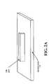
- FIG. 2Aillustrates an exemplary fin consistent with the invention
- FIG. 2Billustrates a cross-sectional view of the exemplary fin of FIG. 2A consistent with the invention
- FIGS. 2C and 2Dillustrate exemplary source and drain regions formed adjacent the fin of FIGS. 2A and 2B consistent with the invention
- FIG. 3Aillustrates a cross-sectional view of a strained layer formed on a fin consistent with the invention
- FIG. 3Billustrates a top view of the strained layer of FIG. 3A formed upon a fin and source and drain regions consistent with the invention
- FIG. 4Aillustrates a cross-sectional view of a gate dielectric and gate electrode formed upon a fin consistent with the invention
- FIG. 4Billustrates a top view of the gate dielectric and gate electrode of FIG. 4A formed upon a fin consistent with the invention
- FIG. 5illustrates a strained insulator underneath the fin of FIGS. 2A and 2B consistent with another embodiment of the present invention.
- FIG. 6illustrates damescene source/drain regrowth consistent with another embodiment of the present invention.
- an increased mobility channel FinFETis provided.
- a vertically formed strained channel layerconsistent with the present invention, is self-aligned to the fin channel of the FinFET.
- the strained channel layermay include a crystalline material that is lattice mismatched with the crystalline material of the fin of the FinFET such that tensile strain is induced within the strained channel layer.
- the induced tensile strainincreases carrier mobility of the strained channel layer, thus, increasing drive current of the FinFET.
- FIG. 1illustrates a cross-section of a substrate 100 formed in accordance with an exemplary embodiment of the present invention.
- Substrate 100may be a silicon on insulator (SOI) structure that includes a fin channel layer 105 formed upon, for example, a buried oxide layer 110 .
- Buried oxide layer 110may be formed on a silicon layer (not shown).
- the thickness of fin channel layer 105may range, for example, from about 500 ⁇ to about 2000 ⁇ and the thickness of buried oxide layer 110 may range, for example, from about 1000 ⁇ to about 3000 ⁇ .
- Fin channel layer 105may include a crystalline material with a lattice constant larger than the lattice constant of a crystalline material selected for a strained channel layer (described with respect to FIGS. 3A and 3B below). If, for example, silicon is selected for the strained channel layer, fin channel layer 105 may include a crystalline material with a lattice constant large than the lattice constant of silicon. Fin channel layer 105 may include, for example, Si x Ge (1-x) with x approximately equal to 0.7. Other values of x may be appropriately selected.
- substrate 100may be formed by wafer bonding epitaxial Si x Ge (1-x) to an oxide/Si substrate wafer.
- substrate 100may be formed by wafer bonding epitaxial Si x Ge (1-x) to an oxide/Si substrate wafer.
- a vertical fin 205may be formed from fin channel layer 105 .
- Fin 205may be formed, for example, with a width (w) in a range of 10-15 nm. Fin 205 may be formed from fin channel layer 105 using any existing process, including, but not limited to, existing photolithographic and etching processes.
- Source 210 and drain 215 regionsmay be formed adjacent the respective ends of fin 205 , as shown in FIGS. 2C and 2D.
- Source 210 and drain 215 regionsmay be formed by, for example, deposition of a layer of crystalline material over fin 205 .
- the source 210 and drain 215 regionsmay be formed from the layer of crystalline material using, for example, existing photolithographic and etching processes.
- One skilled in the artwill recognize, however, that other existing techniques may be used for forming source 210 and drain 215 regions.
- Source 210 and drain 215 regionsmay include a crystalline material such as, for example, Si x Ge (1-x) , with x approximately equal to 0.7.
- a strained layer 305may be formed on fin 205 , source 210 and drain 215 , as shown in FIGS. 3A and 3B.
- Strained layer 305may be formed on fin 205 , source 210 and drain 215 using any appropriate existing process.
- strained layer 305may be formed on fin 205 , source 210 and drain 215 using a selective epitaxial deposition process.
- Strained layer 305may include a crystalline material whose lattice constant is smaller that the lattice constant of the crystalline material used for fin 205 .
- Strained layer 305may be formed, for example, with a thickness t that is approximately ⁇ fraction (1/2) ⁇ to 1 ⁇ 3 of the fin 205 width w.
- the thickness t of strained layer 305may be 5 nm.
- Strained layer 305may include, but is not limited to, silicon.
- siliconOne skilled in the art will recognize that other crystalline materials with lattice constants less than the crystalline material used to form fin 205 may, alternatively, be used.
- a gate dielectric 405 and gate electrode 410may be formed on the portion of fin 205 not covered by source 210 and drain 215 , as shown in FIGS. 4A and 4B.
- the gate dielectric 405may include a thin layer of dielectric material, such as SiO, SiO 2 , SiN, SiON, HFO 2 , ZrO 2 , Al 2 O 3 , HFSiO(x)ZnS, MgF 2 , or other dielectric materials.
- Gate electrode 410may be formed upon gate dielectric 405 and may include, for example, a layer of polysilicon.
- Gate dielectric 405 and gate electrode 410may be formed on fin 205 using any existing processes, such as, for example, existing deposition and patterning processes. Formation of gate dielectric 405 and gate electrode 410 upon fin 205 , thus, produces a FET sidewall vertical channel that includes a thin strained layer 305 at both vertical surfaces of fin 205 . Strained layer 305 provides improved carrier mobility through the induction of tensile strain in strained layer 305 caused by the lattice mismatch between strained layer 305 and fin 205 . This carrier mobility enhancement can increase the drive current of a FinFET transistor created using the semiconductor structure shown in FIGS. 4A and 4B.
- FIG. 5illustrates an exemplary strained insulator 505 that may, consistent with another embodiment of the present invention, be formed beneath a fin of a FinFET, such as fin 205 shown in FIGS. 2A and 2B.
- Fin 205may be formed upon the insulating material of strained insulator 505 such that the crystalline material of fin 205 and strained insulator 505 are lattice mismatched.
- a lattice mismatch between fin 205 and strained insulator 505produces tensile strain in fin 205 that, in turn, improves carrier mobility of the FinFET.
- any appropriate insulating materialwith a lattice constant that is mismatched with the crystalline material of fin 205 , may be used as strained insulator 505 .
- FIG. 6illustrates exemplary damascene source/drain regrowth consistent with another embodiment of the present invention.
- TEOStetraethylorthosilicate
- a mask (mask 1 ) 610may then be used to open a gate area 615 .
- Fin 605may be thinned down and a gate 620 may be formed by depositing and polishing polysilicon in gate area 615 .
- a second mask (mask 2 ) 625may be used to open a source and drain area 630 .
- a nitride layer of active area 600within the opened source and drain area 630 , may be etched to expose a region of the source and drain area 630 . From the exposed region, silicon can be selectively re-grown to produce a source 635 and a drain 640 .
Landscapes
- Thin Film Transistor (AREA)
- Insulated Gate Type Field-Effect Transistor (AREA)
Abstract
Description
- The present invention relates generally to transistors and, more particularly, to fin field effect transistors (FinFETs).[0001]
- Scaling of device dimensions has been a primary factor driving improvements in integrated circuit performance and reduction in integrated circuit cost. Due to limitations associated with existing gate-oxide thicknesses and source/drain (S/D) junction depths, scaling of existing bulk MOSFET devices below the 0.1 μm process generation may be difficult, if not impossible. New device structures and new materials, thus, are likely to be needed to improve FET performance.[0002]
- Double-gate MOSFETs represent new devices that are candidates for succeeding existing planar MOSFETs. In double-gate MOSFETs, the use of two gates to control the channel significantly suppresses short-channel effects. A FinFET is a recent double-gate structure that includes a channel formed in a vertical fin. The FinFET is similar to existing planar MOSFET in layout and fabrication. The FinFET also provides a range of channel lengths, CMOS compatibility and large packing density compared to other double-gate structures.[0003]
- Consistent with the present invention, a FinFET transistor is provided that uses a vertically formed strained channel layer that is self-aligned to the fin channel. The strained channel layer may include a crystalline material that is lattice constant mismatched with the crystalline material of the fin of the FinFET. The lattice constant mismatch induces tensile strain within the strained channel layer that increases carrier mobility. Increasing the carrier mobility, in turn, increases the drive current of the FinFET transistor, thus, improving FinFET performance.[0004]
- Additional advantages and other features of the invention will be set forth in part in the description which follows and, in part, will become apparent to those having ordinary skill in the art upon examination of the following, or may be learned from the practice of the invention. The advantages and features of the invention may be realized and obtained as particularly pointed out in the appended claims.[0005]
- According to the present invention, the foregoing and other advantages are achieved in part by a semiconductor structure that includes a fin. The fin includes a first crystalline material and a plurality of surfaces. The structure further includes a layer formed on at least a portion of the plurality of surfaces, the layer including a second crystalline material. The first crystalline material has a different lattice constant than the second crystalline material to induce tensile strain within the layer.[0006]
- According to another aspect of the invention, a transistor is provided. The transistor includes a fin that further includes a first crystalline material and first and second end portions. The first crystalline material has a first lattice constant. The transistor further includes source and drain regions formed adjacent the first and second end portions of the fin. The transistor also includes a first layer of second crystalline material formed on at least a portion of the fin. The second crystalline material has a second lattice constant, wherein the first lattice constant is greater than the second lattice constant. The transistor additionally includes a dielectric layer formed on at least a portion of the first layer and a gate electrode formed on at least a portion of the dielectric layer.[0007]
- According to a further aspect of the invention, a method of forming a semiconductor device is provided. The method includes forming a fin that includes a first crystalline material and multiple surfaces. The method further includes forming a first layer on at least a portion of the multiple surfaces. The first layer includes a second crystalline material, wherein the first crystalline material is lattice constant mismatched with the second crystalline material to induce tensile strain within the first layer.[0008]
- Other advantages and features of the present invention will become readily apparent to those skilled in this art from the following detailed description. The embodiments shown and described provide illustration of the best mode contemplated for carrying out the invention. The invention is capable of modifications in various obvious respects, all without departing from the invention. Accordingly, the drawings are to be regarded as illustrative in nature, and not as restrictive.[0009]
- Reference is made to the attached drawings, wherein elements having the same reference number designation may represent like elements throughout.[0010]
- FIG. 1 illustrates exemplary layers of a substrate that may be used for forming a fin of a FinFET consistent with the present invention;[0011]
- FIG. 2A illustrates an exemplary fin consistent with the invention;[0012]
- FIG. 2B illustrates a cross-sectional view of the exemplary fin of FIG. 2A consistent with the invention;[0013]
- FIGS. 2C and 2D illustrate exemplary source and drain regions formed adjacent the fin of FIGS. 2A and 2B consistent with the invention;[0014]
- FIG. 3A illustrates a cross-sectional view of a strained layer formed on a fin consistent with the invention;[0015]
- FIG. 3B illustrates a top view of the strained layer of FIG. 3A formed upon a fin and source and drain regions consistent with the invention;[0016]
- FIG. 4A illustrates a cross-sectional view of a gate dielectric and gate electrode formed upon a fin consistent with the invention;[0017]
- FIG. 4B illustrates a top view of the gate dielectric and gate electrode of FIG. 4A formed upon a fin consistent with the invention;[0018]
- FIG. 5 illustrates a strained insulator underneath the fin of FIGS. 2A and 2B consistent with another embodiment of the present invention; and[0019]
- FIG. 6 illustrates damescene source/drain regrowth consistent with another embodiment of the present invention.[0020]
- The following detailed description of the invention refers to the accompanying drawings. The same reference numbers in different drawings may identify the same or similar elements. Also, the following detailed description does not limit the invention. Instead, the scope of the invention is defined by the appended claims.[0021]
- Consistent with the present invention, an increased mobility channel FinFET is provided. A vertically formed strained channel layer, consistent with the present invention, is self-aligned to the fin channel of the FinFET. The strained channel layer may include a crystalline material that is lattice mismatched with the crystalline material of the fin of the FinFET such that tensile strain is induced within the strained channel layer. The induced tensile strain increases carrier mobility of the strained channel layer, thus, increasing drive current of the FinFET.[0022]
- FIG. 1 illustrates a cross-section of a[0023]
substrate 100 formed in accordance with an exemplary embodiment of the present invention.Substrate 100, consistent with the present invention, may be a silicon on insulator (SOI) structure that includes afin channel layer 105 formed upon, for example, a buriedoxide layer 110.Buried oxide layer 110 may be formed on a silicon layer (not shown). The thickness offin channel layer 105 may range, for example, from about 500 Å to about 2000 Å and the thickness of buriedoxide layer 110 may range, for example, from about 1000 Å to about 3000 Å. - [0024]
Fin channel layer 105 may include a crystalline material with a lattice constant larger than the lattice constant of a crystalline material selected for a strained channel layer (described with respect to FIGS. 3A and 3B below). If, for example, silicon is selected for the strained channel layer,fin channel layer 105 may include a crystalline material with a lattice constant large than the lattice constant of silicon.Fin channel layer 105 may include, for example, SixGe(1-x)with x approximately equal to 0.7. Other values of x may be appropriately selected. One skilled in the art will recognize that crystalline materials other than SixGe(1-x)may be used such that the material's lattice constant is larger than the lattice constant of the crystalline material selected for the strained channel layer. In some embodiments,substrate 100 may be formed by wafer bonding epitaxial SixGe(1-x)to an oxide/Si substrate wafer. One skilled in the art will recognize, however, that other existing techniques may be used for formingsubstrate 100. - As shown in FIGS. 2A and 2B, after forming[0025]
substrate 100, avertical fin 205 may be formed fromfin channel layer 105.Fin 205 may be formed, for example, with a width (w) in a range of 10-15 nm.Fin 205 may be formed fromfin channel layer 105 using any existing process, including, but not limited to, existing photolithographic and etching processes. - Subsequent to formation of[0026]
fin 205,source 210 and drain215 regions may be formed adjacent the respective ends offin 205, as shown in FIGS. 2C and 2D.Source 210 and drain215 regions may be formed by, for example, deposition of a layer of crystalline material overfin 205. Thesource 210 and drain215 regions may be formed from the layer of crystalline material using, for example, existing photolithographic and etching processes. One skilled in the art will recognize, however, that other existing techniques may be used for formingsource 210 and drain215 regions.Source 210 and drain215 regions may include a crystalline material such as, for example, SixGe(1-x), with x approximately equal to 0.7. - After formation of[0027]
source 210 and drain215 regions, astrained layer 305 may be formed onfin 205,source 210 and drain215, as shown in FIGS. 3A and 3B.Strained layer 305 may be formed onfin 205,source 210 and drain215 using any appropriate existing process. In some exemplary embodiments, for example,strained layer 305 may be formed onfin 205,source 210 and drain215 using a selective epitaxial deposition process.Strained layer 305 may include a crystalline material whose lattice constant is smaller that the lattice constant of the crystalline material used forfin 205. With a lattice mismatch betweenfin 205 andstrained layer 305 tensile strain is produced instrained layer 305.Strained layer 305 may be formed, for example, with a thickness t that is approximately {fraction (1/2)} to ⅓ of thefin 205 width w. For example, the thickness t ofstrained layer 305 may be 5 nm.Strained layer 305 may include, but is not limited to, silicon. One skilled in the art will recognize that other crystalline materials with lattice constants less than the crystalline material used to formfin 205 may, alternatively, be used. - After formation of[0028]
strained layer 305, agate dielectric 405 andgate electrode 410 may be formed on the portion offin 205 not covered bysource 210 and drain215, as shown in FIGS. 4A and 4B. Thegate dielectric 405 may include a thin layer of dielectric material, such as SiO, SiO2, SiN, SiON, HFO2, ZrO2, Al2O3, HFSiO(x)ZnS, MgF2, or other dielectric materials.Gate electrode 410 may be formed upongate dielectric 405 and may include, for example, a layer of polysilicon.Gate dielectric 405 andgate electrode 410 may be formed onfin 205 using any existing processes, such as, for example, existing deposition and patterning processes. Formation ofgate dielectric 405 andgate electrode 410 uponfin 205, thus, produces a FET sidewall vertical channel that includes a thinstrained layer 305 at both vertical surfaces offin 205.Strained layer 305 provides improved carrier mobility through the induction of tensile strain instrained layer 305 caused by the lattice mismatch betweenstrained layer 305 andfin 205. This carrier mobility enhancement can increase the drive current of a FinFET transistor created using the semiconductor structure shown in FIGS. 4A and 4B. - FIG. 5 illustrates an exemplary[0029]
strained insulator 505 that may, consistent with another embodiment of the present invention, be formed beneath a fin of a FinFET, such asfin 205 shown in FIGS. 2A and 2B.Fin 205 may be formed upon the insulating material ofstrained insulator 505 such that the crystalline material offin 205 andstrained insulator 505 are lattice mismatched. A lattice mismatch betweenfin 205 andstrained insulator 505 produces tensile strain infin 205 that, in turn, improves carrier mobility of the FinFET. One skilled in the art will recognize that any appropriate insulating material, with a lattice constant that is mismatched with the crystalline material offin 205, may be used asstrained insulator 505. - FIG. 6 illustrates exemplary damascene source/drain regrowth consistent with another embodiment of the present invention. After forming an[0030]
active area 600 andfin 605 upon a substrate, tetraethylorthosilicate (TEOS) may be deposited uponfin 605 andactive area 600 and then polished. A mask (mask1)610 may then be used to open agate area 615.Fin 605 may be thinned down and agate 620 may be formed by depositing and polishing polysilicon ingate area 615. A second mask (mask2)625 may be used to open a source anddrain area 630. A nitride layer ofactive area 600, within the opened source anddrain area 630, may be etched to expose a region of the source anddrain area 630. From the exposed region, silicon can be selectively re-grown to produce asource 635 and adrain 640. - In the previous descriptions, numerous specific details are set forth, such as specific materials, structures, chemicals, processes, etc., in order to provide a thorough understanding of the present invention. However, the present invention can be practiced without resorting to the details specifically set forth herein. In other instances, well known processing structures have not been described in detail, in order not to unnecessarily obscure the thrust of the present invention. In practicing the present invention, conventional photolithographic and etching techniques may be employed, and hence, the details of such techniques have not been set forth herein in detail.[0031]
- Only the preferred embodiments of the invention and a few examples of its versatility are shown and described in the present disclosure. It is to be understood that the invention is capable of use in various other combinations and environments and is capable of modifications within the scope of the inventive concept as expressed herein.[0032]
Claims (25)
1. A semiconductor device, comprising:
a fin comprising a first crystalline material and a plurality of surfaces; and
a first layer formed on at least a portion of the plurality of surfaces, the first layer comprising a second crystalline material, wherein the first crystalline material has a different lattice constant than the second crystalline material to induce tensile strain within the first layer.
2. The semiconductor device ofclaim 1 , wherein the fin has a rectangular cross-section.
3. The semiconductor device ofclaim 1 , wherein the first crystalline material comprises a crystalline material with a lattice constant larger than a lattice constant of the second crystalline material.
4. The semiconductor device ofclaim 1 , wherein the second crystalline material comprises silicon.
5. The semiconductor device ofclaim 4 , wherein the first crystalline material comprises a crystalline material with a lattice constant larger than silicon.
6. The semiconductor device ofclaim 5 , wherein the first crystalline material comprises SixGe(1-x).
7. The semiconductor device ofclaim 6 , wherein x equals approximately 0.7.
8. The semiconductor device ofclaim 1 , further comprising:
a second layer formed on at least a portion of the first layer, the second layer comprising a dielectric.
9. The semiconductor device ofclaim 8 , further comprising:
a gate electrode formed on at least a portion of the second layer, the gate electrode comprising polysilicon.
10. A transistor, comprising:
a fin comprising a first crystalline material that has a first lattice constant, the fin further comprising first and second end portions;
source and drain regions formed adjacent the first and second end portions of the fin;
a first layer of second crystalline material formed on at least a portion of the fin, the second crystalline material having a second lattice constant, wherein the first lattice constant is greater than the second lattice constant;
a dielectric layer formed on at least a portion of the first layer; and
a gate electrode formed on at least a portion of the dielectric layer.
11. The transistor ofclaim 10 , wherein the gate electrode comprises a third crystalline material.
12. The transistor ofclaim 11 , wherein the third crystalline material comprises polysilicon.
13. The transistor ofclaim 10 , wherein the first crystalline material comprises SixGe(1-x).
14. The transistor ofclaim 13 , wherein the second crystalline material comprises silicon.
15. The transistor ofclaim 13 , wherein x equals approximately 0.7.
16. The transistor ofclaim 10 , wherein the first lattice constant is greater than the second lattice constant to induce tensile strain in the first layer.
17. The transistor ofclaim 16 , wherein the tensile strain increases carrier mobility in the first layer.
18. A method of forming a semiconductor device, comprising:
forming a fin comprising a first crystalline material and a plurality of surfaces; and
forming a first layer on at least a portion of the plurality of surfaces, the first layer comprising a second crystalline material, wherein the first crystalline material is lattice constant mismatched with the second crystalline material to induce tensile strain within the first layer.
19. The method ofclaim 18 , further comprising:
selecting the first crystalline material such that the first crystalline material has a lattice constant greater than a lattice constant of the second crystalline material.
20. The method ofclaim 18 , further comprising:
selecting silicon as the second crystalline material for forming the first layer.
21. The method ofclaim 20 , further comprising:
selecting the first crystalline material such that the first crystalline material has a lattice constant larger than silicon.
22. The method of21, further comprising:
selecting SixGe(1-x)as the first crystalline material for forming the elongated fin.
23. The method ofclaim 22 , further comprising:
selecting x as approximately equal to 0.7.
24. The method of claim ofclaim 18 , further comprising:
forming a second layer on the first layer, the second layer comprising a dielectric.
25. The method ofclaim 24 , further comprising:
forming a gate electrode on the second layer, the gate electrode comprising polysilicon.
Priority Applications (8)
| Application Number | Priority Date | Filing Date | Title |
|---|---|---|---|
| US10/349,042US6803631B2 (en) | 2003-01-23 | 2003-01-23 | Strained channel finfet |
| KR1020057013666AKR20050096155A (en) | 2003-01-23 | 2004-01-15 | Strained channel finfet |
| CNB200480002593XACN100521230C (en) | 2003-01-23 | 2004-01-15 | Strained channel FinFET |
| EP04702513.5AEP1593161B1 (en) | 2003-01-23 | 2004-01-15 | Strained channel finfet |
| PCT/US2004/000967WO2004068585A1 (en) | 2003-01-23 | 2004-01-15 | Strained channel finfet |
| JP2006502829AJP2006516821A (en) | 2003-01-23 | 2004-01-15 | Method for forming strained channel fin FET |
| TW093101515ATWI326489B (en) | 2003-01-23 | 2004-01-20 | Strained channel finfet |
| US10/833,112US6897527B2 (en) | 2003-01-23 | 2004-04-28 | Strained channel FinFET |
Applications Claiming Priority (1)
| Application Number | Priority Date | Filing Date | Title |
|---|---|---|---|
| US10/349,042US6803631B2 (en) | 2003-01-23 | 2003-01-23 | Strained channel finfet |
Related Child Applications (1)
| Application Number | Title | Priority Date | Filing Date |
|---|---|---|---|
| US10/833,112ContinuationUS6897527B2 (en) | 2003-01-23 | 2004-04-28 | Strained channel FinFET |
Publications (2)
| Publication Number | Publication Date |
|---|---|
| US20040145019A1true US20040145019A1 (en) | 2004-07-29 |
| US6803631B2 US6803631B2 (en) | 2004-10-12 |
Family
ID=32735412
Family Applications (2)
| Application Number | Title | Priority Date | Filing Date |
|---|---|---|---|
| US10/349,042Expired - LifetimeUS6803631B2 (en) | 2003-01-23 | 2003-01-23 | Strained channel finfet |
| US10/833,112Expired - LifetimeUS6897527B2 (en) | 2003-01-23 | 2004-04-28 | Strained channel FinFET |
Family Applications After (1)
| Application Number | Title | Priority Date | Filing Date |
|---|---|---|---|
| US10/833,112Expired - LifetimeUS6897527B2 (en) | 2003-01-23 | 2004-04-28 | Strained channel FinFET |
Country Status (7)
| Country | Link |
|---|---|
| US (2) | US6803631B2 (en) |
| EP (1) | EP1593161B1 (en) |
| JP (1) | JP2006516821A (en) |
| KR (1) | KR20050096155A (en) |
| CN (1) | CN100521230C (en) |
| TW (1) | TWI326489B (en) |
| WO (1) | WO2004068585A1 (en) |
Cited By (34)
| Publication number | Priority date | Publication date | Assignee | Title |
|---|---|---|---|---|
| US20030201458A1 (en)* | 2002-03-19 | 2003-10-30 | Clark William F. | Strained fin fets structure and method |
| US20040094807A1 (en)* | 2002-08-23 | 2004-05-20 | Chau Robert S. | Tri-gate devices and methods of fabrication |
| US20040188670A1 (en)* | 2003-03-31 | 2004-09-30 | Shaheed M. Reaz | Increasing stress-enhanced drive current in a MOS transistor |
| US20050173740A1 (en)* | 2004-02-07 | 2005-08-11 | You-Seung Jin | Multi-gate transistor formed with active patterns of uniform critical dimension |
| US20050287772A1 (en)* | 2004-06-07 | 2005-12-29 | Infineon Technologies Ag | Process for producing a web of a semiconductor material |
| US20060033095A1 (en)* | 2004-08-10 | 2006-02-16 | Doyle Brian S | Non-planar pMOS structure with a strained channel region and an integrated strained CMOS flow |
| US20060076625A1 (en)* | 2004-09-25 | 2006-04-13 | Lee Sung-Young | Field effect transistors having a strained silicon channel and methods of fabricating same |
| US20060157794A1 (en)* | 2005-01-18 | 2006-07-20 | Doyle Brian S | Non-planar MOS structure with a strained channel region |
| US7084018B1 (en)* | 2004-05-05 | 2006-08-01 | Advanced Micro Devices, Inc. | Sacrificial oxide for minimizing box undercut in damascene FinFET |
| US20060261411A1 (en)* | 2003-06-27 | 2006-11-23 | Hareland Scott A | Nonplanar device with stress incorporation layer and method of fabrication |
| US20080061284A1 (en)* | 2006-09-11 | 2008-03-13 | International Business Machines Corporation | Nanowire MOSFET with doped epitaxial contacts for source and drain |
| WO2007133775A3 (en)* | 2006-05-15 | 2008-05-29 | Univ Carnegie Mellon | Integrated circuit, device, system, and method of fabrication |
| US20080137051A1 (en)* | 2004-12-21 | 2008-06-12 | Carnegie Mellon University | Lithography and Associated Methods, Devices, and Systems |
| US20080179682A1 (en)* | 2007-01-31 | 2008-07-31 | Infineon Technologies Ag | Circuit layout for different performance and method |
| US7456476B2 (en) | 2003-06-27 | 2008-11-25 | Intel Corporation | Nonplanar semiconductor device with partially or fully wrapped around gate electrode and methods of fabrication |
| US7479421B2 (en) | 2005-09-28 | 2009-01-20 | Intel Corporation | Process for integrating planar and non-planar CMOS transistors on a bulk substrate and article made thereby |
| DE102005045078B4 (en)* | 2004-09-25 | 2009-01-22 | Samsung Electronics Co., Ltd., Suwon | Field effect transistor with a strained channel layer on sidewalls of a structure on a semiconductor substrate |
| US7547637B2 (en) | 2005-06-21 | 2009-06-16 | Intel Corporation | Methods for patterning a semiconductor film |
| US7736956B2 (en) | 2005-08-17 | 2010-06-15 | Intel Corporation | Lateral undercut of metal gate in SOI device |
| US7781771B2 (en) | 2004-03-31 | 2010-08-24 | Intel Corporation | Bulk non-planar transistor having strained enhanced mobility and methods of fabrication |
| US7879675B2 (en) | 2005-03-14 | 2011-02-01 | Intel Corporation | Field effect transistor with metal source/drain regions |
| US7898041B2 (en) | 2005-06-30 | 2011-03-01 | Intel Corporation | Block contact architectures for nanoscale channel transistors |
| US7902014B2 (en) | 2005-09-28 | 2011-03-08 | Intel Corporation | CMOS devices with a single work function gate electrode and method of fabrication |
| US7989280B2 (en) | 2005-11-30 | 2011-08-02 | Intel Corporation | Dielectric interface for group III-V semiconductor device |
| US8067818B2 (en) | 2004-10-25 | 2011-11-29 | Intel Corporation | Nonplanar device with thinned lower body portion and method of fabrication |
| US8084818B2 (en) | 2004-06-30 | 2011-12-27 | Intel Corporation | High mobility tri-gate devices and methods of fabrication |
| US8183646B2 (en) | 2005-02-23 | 2012-05-22 | Intel Corporation | Field effect transistor with narrow bandgap source and drain regions and method of fabrication |
| US8268709B2 (en) | 2004-09-29 | 2012-09-18 | Intel Corporation | Independently accessed double-gate and tri-gate transistors in same process flow |
| US8362566B2 (en) | 2008-06-23 | 2013-01-29 | Intel Corporation | Stress in trigate devices using complimentary gate fill materials |
| US8617945B2 (en) | 2006-08-02 | 2013-12-31 | Intel Corporation | Stacking fault and twin blocking barrier for integrating III-V on Si |
| US9093516B2 (en) | 2012-12-07 | 2015-07-28 | Imec | Semiconductor heterostructure field effect transistor and method for making thereof |
| US9337307B2 (en) | 2005-06-15 | 2016-05-10 | Intel Corporation | Method for fabricating transistor with thinned channel |
| US9589811B2 (en)* | 2015-06-24 | 2017-03-07 | Varian Semiconductor Equipment Associates, Inc. | FinFET spacer etch with no fin recess and no gate-spacer pull-down |
| GB2542973A (en)* | 2012-12-20 | 2017-04-05 | Intel Corp | Expitaxial film on nanoscale structure |
Families Citing this family (61)
| Publication number | Priority date | Publication date | Assignee | Title |
|---|---|---|---|---|
| US7091068B1 (en)* | 2002-12-06 | 2006-08-15 | Advanced Micro Devices, Inc. | Planarizing sacrificial oxide to improve gate critical dimension in semiconductor devices |
| WO2004073044A2 (en)* | 2003-02-13 | 2004-08-26 | Massachusetts Institute Of Technology | Finfet device and method to make same |
| TWI231994B (en)* | 2003-04-04 | 2005-05-01 | Univ Nat Taiwan | Strained Si FinFET |
| CN1799146A (en)* | 2003-05-30 | 2006-07-05 | 松下电器产业株式会社 | Semiconductor device and method for manufacturing same |
| US7045401B2 (en)* | 2003-06-23 | 2006-05-16 | Sharp Laboratories Of America, Inc. | Strained silicon finFET device |
| US6921982B2 (en)* | 2003-07-21 | 2005-07-26 | International Business Machines Corporation | FET channel having a strained lattice structure along multiple surfaces |
| EP1519420A2 (en)* | 2003-09-25 | 2005-03-30 | Interuniversitaire Microelectronica Centrum vzw ( IMEC) | Multiple gate semiconductor device and method for forming same |
| US6855989B1 (en)* | 2003-10-01 | 2005-02-15 | Advanced Micro Devices, Inc. | Damascene finfet gate with selective metal interdiffusion |
| US6970373B2 (en)* | 2003-10-02 | 2005-11-29 | Intel Corporation | Method and apparatus for improving stability of a 6T CMOS SRAM cell |
| US7144818B2 (en)* | 2003-12-05 | 2006-12-05 | Advanced Micro Devices, Inc. | Semiconductor substrate and processes therefor |
| US6924178B2 (en)* | 2003-12-08 | 2005-08-02 | International Business Machines Corporation | Oxide/nitride stacked in FinFET spacer process |
| US7198995B2 (en)* | 2003-12-12 | 2007-04-03 | International Business Machines Corporation | Strained finFETs and method of manufacture |
| US6936516B1 (en)* | 2004-01-12 | 2005-08-30 | Advanced Micro Devices, Inc. | Replacement gate strained silicon finFET process |
| US7268058B2 (en)* | 2004-01-16 | 2007-09-11 | Intel Corporation | Tri-gate transistors and methods to fabricate same |
| US7005302B2 (en)* | 2004-04-07 | 2006-02-28 | Advanced Micro Devices, Inc. | Semiconductor on insulator substrate and devices formed therefrom |
| US7176092B2 (en)* | 2004-04-16 | 2007-02-13 | Taiwan Semiconductor Manufacturing Company | Gate electrode for a semiconductor fin device |
| US7579280B2 (en)* | 2004-06-01 | 2009-08-25 | Intel Corporation | Method of patterning a film |
| US7262104B1 (en) | 2004-06-02 | 2007-08-28 | Advanced Micro Devices, Inc. | Selective channel implantation for forming semiconductor devices with different threshold voltages |
| US7332439B2 (en) | 2004-09-29 | 2008-02-19 | Intel Corporation | Metal gate transistors with epitaxial source and drain regions |
| JP4064955B2 (en)* | 2004-09-30 | 2008-03-19 | 株式会社東芝 | Semiconductor device and manufacturing method thereof |
| US7361958B2 (en) | 2004-09-30 | 2008-04-22 | Intel Corporation | Nonplanar transistors with metal gate electrodes |
| JP2006135067A (en)* | 2004-11-05 | 2006-05-25 | Toshiba Corp | Semiconductor device and manufacturing method thereof |
| US7400031B2 (en)* | 2005-09-19 | 2008-07-15 | International Business Machines Corporation | Asymmetrically stressed CMOS FinFET |
| US7309626B2 (en)* | 2005-11-15 | 2007-12-18 | International Business Machines Corporation | Quasi self-aligned source/drain FinFET process |
| US7402856B2 (en)* | 2005-12-09 | 2008-07-22 | Intel Corporation | Non-planar microelectronic device having isolation element to mitigate fringe effects and method to fabricate same |
| DE102005059231B4 (en)* | 2005-12-12 | 2011-01-13 | Infineon Technologies Ag | A method of fabricating a compound semiconductor field effect transistor having a fin structure and compound semiconductor field effect transistor having a fin structure |
| US7439588B2 (en)* | 2005-12-13 | 2008-10-21 | Intel Corporation | Tri-gate integration with embedded floating body memory cell using a high-K dual metal gate |
| US7512017B2 (en)* | 2005-12-21 | 2009-03-31 | Intel Corporation | Integration of planar and tri-gate devices on the same substrate |
| US7396711B2 (en) | 2005-12-27 | 2008-07-08 | Intel Corporation | Method of fabricating a multi-cornered film |
| US7525160B2 (en) | 2005-12-27 | 2009-04-28 | Intel Corporation | Multigate device with recessed strain regions |
| US20070148926A1 (en)* | 2005-12-28 | 2007-06-28 | Intel Corporation | Dual halo implant for improving short channel effect in three-dimensional tri-gate transistors |
| US20070235763A1 (en)* | 2006-03-29 | 2007-10-11 | Doyle Brian S | Substrate band gap engineered multi-gate pMOS devices |
| US7449373B2 (en) | 2006-03-31 | 2008-11-11 | Intel Corporation | Method of ion implanting for tri-gate devices |
| US7407847B2 (en)* | 2006-03-31 | 2008-08-05 | Intel Corporation | Stacked multi-gate transistor design and method of fabrication |
| US7425500B2 (en) | 2006-03-31 | 2008-09-16 | Intel Corporation | Uniform silicide metal on epitaxially grown source and drain regions of three-dimensional transistors |
| US7442590B2 (en)* | 2006-04-27 | 2008-10-28 | Freescale Semiconductor, Inc | Method for forming a semiconductor device having a fin and structure thereof |
| JP2007299951A (en)* | 2006-04-28 | 2007-11-15 | Toshiba Corp | Semiconductor device and manufacturing method thereof |
| US7435683B2 (en)* | 2006-09-15 | 2008-10-14 | Intel Corporation | Apparatus and method for selectively recessing spacers on multi-gate devices |
| US7700470B2 (en) | 2006-09-22 | 2010-04-20 | Intel Corporation | Selective anisotropic wet etching of workfunction metal for semiconductor devices |
| US7538391B2 (en)* | 2007-01-09 | 2009-05-26 | International Business Machines Corporation | Curved FINFETs |
| US20080173942A1 (en)* | 2007-01-22 | 2008-07-24 | International Business Machines Corporation | STRUCTURE AND METHOD OF MANUFACTURING A STRAINED FinFET WITH STRESSED SILICIDE |
| KR20100048954A (en)* | 2007-07-27 | 2010-05-11 | 파나소닉 주식회사 | Semiconductor device and method for manufacturing the same |
| US7910994B2 (en)* | 2007-10-15 | 2011-03-22 | Taiwan Semiconductor Manufacturing Company, Ltd. | System and method for source/drain contact processing |
| US8053838B2 (en)* | 2008-06-26 | 2011-11-08 | International Business Machines Corporation | Structures, fabrication methods, design structures for strained fin field effect transistors (FinFets) |
| US20100155801A1 (en)* | 2008-12-22 | 2010-06-24 | Doyle Brian S | Integrated circuit, 1T-1C embedded memory cell containing same, and method of manufacturing 1T-1C memory cell for embedded memory application |
| US7999298B2 (en)* | 2008-12-30 | 2011-08-16 | Intel Corporation | Embedded memory cell and method of manufacturing same |
| US9768305B2 (en)* | 2009-05-29 | 2017-09-19 | Taiwan Semiconductor Manufacturing Company, Ltd. | Gradient ternary or quaternary multiple-gate transistor |
| US7977174B2 (en)* | 2009-06-08 | 2011-07-12 | Globalfoundries Inc. | FinFET structures with stress-inducing source/drain-forming spacers and methods for fabricating the same |
| US20100308409A1 (en)* | 2009-06-08 | 2010-12-09 | Globalfoundries Inc. | Finfet structures with fins having stress-inducing caps and methods for fabricating the same |
| US8404592B2 (en)* | 2009-07-27 | 2013-03-26 | GlobalFoundries, Inc. | Methods for fabricating FinFET semiconductor devices using L-shaped spacers |
| US8629478B2 (en)* | 2009-07-31 | 2014-01-14 | Taiwan Semiconductor Manufacturing Company, Ltd. | Fin structure for high mobility multiple-gate transistor |
| CN102315269B (en)* | 2010-07-01 | 2013-12-25 | 中国科学院微电子研究所 | Semiconductor device and forming method thereof |
| CN103137671B (en)* | 2011-12-02 | 2015-06-24 | 中芯国际集成电路制造(上海)有限公司 | Multi-grid field effect transistor and manufacturing method thereof |
| CN103187446B (en)* | 2011-12-31 | 2016-02-03 | 中芯国际集成电路制造(上海)有限公司 | Multiple gate field effect transistor and manufacture method thereof |
| US8729634B2 (en)* | 2012-06-15 | 2014-05-20 | Taiwan Semiconductor Manufacturing Company, Ltd. | FinFET with high mobility and strain channel |
| US8872225B2 (en)* | 2012-12-20 | 2014-10-28 | Intel Corporation | Defect transferred and lattice mismatched epitaxial film |
| US9391181B2 (en) | 2012-12-21 | 2016-07-12 | Intel Corporation | Lattice mismatched hetero-epitaxial film |
| US8823060B1 (en)* | 2013-02-20 | 2014-09-02 | Taiwan Semiconductor Manufacturing Co., Ltd. | Method for inducing strain in FinFET channels |
| US9214555B2 (en) | 2013-03-12 | 2015-12-15 | Taiwan Semiconductor Manufacturing Co., Ltd. | Barrier layer for FinFET channels |
| EP3123519A4 (en) | 2014-03-24 | 2017-10-25 | Intel Corporation | Fin sculpting and cladding during replacement gate process for transistor channel applications |
| US9755073B1 (en) | 2016-05-11 | 2017-09-05 | International Business Machines Corporation | Fabrication of vertical field effect transistor structure with strained channels |
Citations (3)
| Publication number | Priority date | Publication date | Assignee | Title |
|---|---|---|---|---|
| US6475869B1 (en)* | 2001-02-26 | 2002-11-05 | Advanced Micro Devices, Inc. | Method of forming a double gate transistor having an epitaxial silicon/germanium channel region |
| US6611029B1 (en)* | 2002-11-08 | 2003-08-26 | Advanced Micro Devices, Inc. | Double gate semiconductor device having separate gates |
| US6635909B2 (en)* | 2002-03-19 | 2003-10-21 | International Business Machines Corporation | Strained fin FETs structure and method |
Family Cites Families (4)
| Publication number | Priority date | Publication date | Assignee | Title |
|---|---|---|---|---|
| US7163864B1 (en)* | 2000-10-18 | 2007-01-16 | International Business Machines Corporation | Method of fabricating semiconductor side wall fin |
| US6300182B1 (en)* | 2000-12-11 | 2001-10-09 | Advanced Micro Devices, Inc. | Field effect transistor having dual gates with asymmetrical doping for reduced threshold voltage |
| JP3782021B2 (en)* | 2002-02-22 | 2006-06-07 | 株式会社東芝 | Semiconductor device, semiconductor device manufacturing method, and semiconductor substrate manufacturing method |
| US6800910B2 (en)* | 2002-09-30 | 2004-10-05 | Advanced Micro Devices, Inc. | FinFET device incorporating strained silicon in the channel region |
- 2003
- 2003-01-23USUS10/349,042patent/US6803631B2/ennot_activeExpired - Lifetime
- 2004
- 2004-01-15EPEP04702513.5Apatent/EP1593161B1/ennot_activeExpired - Lifetime
- 2004-01-15WOPCT/US2004/000967patent/WO2004068585A1/enactiveSearch and Examination
- 2004-01-15JPJP2006502829Apatent/JP2006516821A/enactivePending
- 2004-01-15KRKR1020057013666Apatent/KR20050096155A/ennot_activeAbandoned
- 2004-01-15CNCNB200480002593XApatent/CN100521230C/ennot_activeExpired - Fee Related
- 2004-01-20TWTW093101515Apatent/TWI326489B/ennot_activeIP Right Cessation
- 2004-04-28USUS10/833,112patent/US6897527B2/ennot_activeExpired - Lifetime
Patent Citations (3)
| Publication number | Priority date | Publication date | Assignee | Title |
|---|---|---|---|---|
| US6475869B1 (en)* | 2001-02-26 | 2002-11-05 | Advanced Micro Devices, Inc. | Method of forming a double gate transistor having an epitaxial silicon/germanium channel region |
| US6635909B2 (en)* | 2002-03-19 | 2003-10-21 | International Business Machines Corporation | Strained fin FETs structure and method |
| US6611029B1 (en)* | 2002-11-08 | 2003-08-26 | Advanced Micro Devices, Inc. | Double gate semiconductor device having separate gates |
Cited By (90)
| Publication number | Priority date | Publication date | Assignee | Title |
|---|---|---|---|---|
| US6849884B2 (en)* | 2002-03-19 | 2005-02-01 | International Business Machines Corporation | Strained Fin FETs structure and method |
| US20030201458A1 (en)* | 2002-03-19 | 2003-10-30 | Clark William F. | Strained fin fets structure and method |
| US7358121B2 (en) | 2002-08-23 | 2008-04-15 | Intel Corporation | Tri-gate devices and methods of fabrication |
| US20070034972A1 (en)* | 2002-08-23 | 2007-02-15 | Chau Robert S | Tri-gate devices and methods of fabrication |
| US7560756B2 (en) | 2002-08-23 | 2009-07-14 | Intel Corporation | Tri-gate devices and methods of fabrication |
| US20040094807A1 (en)* | 2002-08-23 | 2004-05-20 | Chau Robert S. | Tri-gate devices and methods of fabrication |
| US7504678B2 (en) | 2002-08-23 | 2009-03-17 | Intel Corporation | Tri-gate devices and methods of fabrication |
| US20040188670A1 (en)* | 2003-03-31 | 2004-09-30 | Shaheed M. Reaz | Increasing stress-enhanced drive current in a MOS transistor |
| US6870179B2 (en)* | 2003-03-31 | 2005-03-22 | Intel Corporation | Increasing stress-enhanced drive current in a MOS transistor |
| US7456476B2 (en) | 2003-06-27 | 2008-11-25 | Intel Corporation | Nonplanar semiconductor device with partially or fully wrapped around gate electrode and methods of fabrication |
| US7820513B2 (en) | 2003-06-27 | 2010-10-26 | Intel Corporation | Nonplanar semiconductor device with partially or fully wrapped around gate electrode and methods of fabrication |
| US20110020987A1 (en)* | 2003-06-27 | 2011-01-27 | Hareland Scott A | Nonplanar semiconductor device with partially or fully wrapped around gate electrode and methods of fabrication |
| US8405164B2 (en) | 2003-06-27 | 2013-03-26 | Intel Corporation | Tri-gate transistor device with stress incorporation layer and method of fabrication |
| US20060261411A1 (en)* | 2003-06-27 | 2006-11-23 | Hareland Scott A | Nonplanar device with stress incorporation layer and method of fabrication |
| US7714397B2 (en) | 2003-06-27 | 2010-05-11 | Intel Corporation | Tri-gate transistor device with stress incorporation layer and method of fabrication |
| US8273626B2 (en) | 2003-06-27 | 2012-09-25 | Intel Corporationn | Nonplanar semiconductor device with partially or fully wrapped around gate electrode and methods of fabrication |
| US7244666B2 (en)* | 2004-02-07 | 2007-07-17 | Samsung Electronics Co., Ltd. | Multi-gate transistor formed with active patterns of uniform critical dimension |
| US20050173740A1 (en)* | 2004-02-07 | 2005-08-11 | You-Seung Jin | Multi-gate transistor formed with active patterns of uniform critical dimension |
| US7781771B2 (en) | 2004-03-31 | 2010-08-24 | Intel Corporation | Bulk non-planar transistor having strained enhanced mobility and methods of fabrication |
| US7084018B1 (en)* | 2004-05-05 | 2006-08-01 | Advanced Micro Devices, Inc. | Sacrificial oxide for minimizing box undercut in damascene FinFET |
| US20050287772A1 (en)* | 2004-06-07 | 2005-12-29 | Infineon Technologies Ag | Process for producing a web of a semiconductor material |
| US8084818B2 (en) | 2004-06-30 | 2011-12-27 | Intel Corporation | High mobility tri-gate devices and methods of fabrication |
| US20060033095A1 (en)* | 2004-08-10 | 2006-02-16 | Doyle Brian S | Non-planar pMOS structure with a strained channel region and an integrated strained CMOS flow |
| US7348284B2 (en) | 2004-08-10 | 2008-03-25 | Intel Corporation | Non-planar pMOS structure with a strained channel region and an integrated strained CMOS flow |
| US7960794B2 (en) | 2004-08-10 | 2011-06-14 | Intel Corporation | Non-planar pMOS structure with a strained channel region and an integrated strained CMOS flow |
| US20060076625A1 (en)* | 2004-09-25 | 2006-04-13 | Lee Sung-Young | Field effect transistors having a strained silicon channel and methods of fabricating same |
| DE102005045078B4 (en)* | 2004-09-25 | 2009-01-22 | Samsung Electronics Co., Ltd., Suwon | Field effect transistor with a strained channel layer on sidewalls of a structure on a semiconductor substrate |
| US8399922B2 (en) | 2004-09-29 | 2013-03-19 | Intel Corporation | Independently accessed double-gate and tri-gate transistors |
| US8268709B2 (en) | 2004-09-29 | 2012-09-18 | Intel Corporation | Independently accessed double-gate and tri-gate transistors in same process flow |
| US9190518B2 (en) | 2004-10-25 | 2015-11-17 | Intel Corporation | Nonplanar device with thinned lower body portion and method of fabrication |
| US8067818B2 (en) | 2004-10-25 | 2011-11-29 | Intel Corporation | Nonplanar device with thinned lower body portion and method of fabrication |
| US9741809B2 (en) | 2004-10-25 | 2017-08-22 | Intel Corporation | Nonplanar device with thinned lower body portion and method of fabrication |
| US8749026B2 (en) | 2004-10-25 | 2014-06-10 | Intel Corporation | Nonplanar device with thinned lower body portion and method of fabrication |
| US8502351B2 (en) | 2004-10-25 | 2013-08-06 | Intel Corporation | Nonplanar device with thinned lower body portion and method of fabrication |
| US10236356B2 (en) | 2004-10-25 | 2019-03-19 | Intel Corporation | Nonplanar device with thinned lower body portion and method of fabrication |
| US20080137051A1 (en)* | 2004-12-21 | 2008-06-12 | Carnegie Mellon University | Lithography and Associated Methods, Devices, and Systems |
| US8259286B2 (en) | 2004-12-21 | 2012-09-04 | Carnegie Mellon University | Lithography and associated methods, devices, and systems |
| US7531393B2 (en) | 2005-01-18 | 2009-05-12 | Intel Corporation | Non-planar MOS structure with a strained channel region |
| DE112006000229B4 (en)* | 2005-01-18 | 2016-04-14 | Intel Corporation | Non-planar MOS structure with a strained channel region and method of fabricating such a structure |
| GB2437867B (en)* | 2005-01-18 | 2008-07-09 | Intel Corp | Non-planer mos structure with a strained channel region |
| GB2437867A (en)* | 2005-01-18 | 2007-11-07 | Intel Corp | Non-planer mos structure with a strained channel region |
| US7193279B2 (en) | 2005-01-18 | 2007-03-20 | Intel Corporation | Non-planar MOS structure with a strained channel region |
| WO2006078469A1 (en)* | 2005-01-18 | 2006-07-27 | Intel Corporation | Non-planar mos structure with a strained channel region |
| US20060157687A1 (en)* | 2005-01-18 | 2006-07-20 | Doyle Brian S | Non-planar MOS structure with a strained channel region |
| US20060157794A1 (en)* | 2005-01-18 | 2006-07-20 | Doyle Brian S | Non-planar MOS structure with a strained channel region |
| US9048314B2 (en) | 2005-02-23 | 2015-06-02 | Intel Corporation | Field effect transistor with narrow bandgap source and drain regions and method of fabrication |
| US8368135B2 (en) | 2005-02-23 | 2013-02-05 | Intel Corporation | Field effect transistor with narrow bandgap source and drain regions and method of fabrication |
| US9614083B2 (en) | 2005-02-23 | 2017-04-04 | Intel Corporation | Field effect transistor with narrow bandgap source and drain regions and method of fabrication |
| US10121897B2 (en) | 2005-02-23 | 2018-11-06 | Intel Corporation | Field effect transistor with narrow bandgap source and drain regions and method of fabrication |
| US8183646B2 (en) | 2005-02-23 | 2012-05-22 | Intel Corporation | Field effect transistor with narrow bandgap source and drain regions and method of fabrication |
| US9368583B2 (en) | 2005-02-23 | 2016-06-14 | Intel Corporation | Field effect transistor with narrow bandgap source and drain regions and method of fabrication |
| US8664694B2 (en) | 2005-02-23 | 2014-03-04 | Intel Corporation | Field effect transistor with narrow bandgap source and drain regions and method of fabrication |
| US9748391B2 (en) | 2005-02-23 | 2017-08-29 | Intel Corporation | Field effect transistor with narrow bandgap source and drain regions and method of fabrication |
| US8816394B2 (en) | 2005-02-23 | 2014-08-26 | Intel Corporation | Field effect transistor with narrow bandgap source and drain regions and method of fabrication |
| US7879675B2 (en) | 2005-03-14 | 2011-02-01 | Intel Corporation | Field effect transistor with metal source/drain regions |
| US9337307B2 (en) | 2005-06-15 | 2016-05-10 | Intel Corporation | Method for fabricating transistor with thinned channel |
| US9806195B2 (en) | 2005-06-15 | 2017-10-31 | Intel Corporation | Method for fabricating transistor with thinned channel |
| US11978799B2 (en) | 2005-06-15 | 2024-05-07 | Tahoe Research, Ltd. | Method for fabricating transistor with thinned channel |
| US8933458B2 (en) | 2005-06-21 | 2015-01-13 | Intel Corporation | Semiconductor device structures and methods of forming semiconductor structures |
| US9761724B2 (en) | 2005-06-21 | 2017-09-12 | Intel Corporation | Semiconductor device structures and methods of forming semiconductor structures |
| US8581258B2 (en) | 2005-06-21 | 2013-11-12 | Intel Corporation | Semiconductor device structures and methods of forming semiconductor structures |
| US7547637B2 (en) | 2005-06-21 | 2009-06-16 | Intel Corporation | Methods for patterning a semiconductor film |
| US9385180B2 (en) | 2005-06-21 | 2016-07-05 | Intel Corporation | Semiconductor device structures and methods of forming semiconductor structures |
| US8071983B2 (en) | 2005-06-21 | 2011-12-06 | Intel Corporation | Semiconductor device structures and methods of forming semiconductor structures |
| US7898041B2 (en) | 2005-06-30 | 2011-03-01 | Intel Corporation | Block contact architectures for nanoscale channel transistors |
| US7736956B2 (en) | 2005-08-17 | 2010-06-15 | Intel Corporation | Lateral undercut of metal gate in SOI device |
| US8294180B2 (en) | 2005-09-28 | 2012-10-23 | Intel Corporation | CMOS devices with a single work function gate electrode and method of fabrication |
| US7902014B2 (en) | 2005-09-28 | 2011-03-08 | Intel Corporation | CMOS devices with a single work function gate electrode and method of fabrication |
| US7479421B2 (en) | 2005-09-28 | 2009-01-20 | Intel Corporation | Process for integrating planar and non-planar CMOS transistors on a bulk substrate and article made thereby |
| US8193567B2 (en) | 2005-09-28 | 2012-06-05 | Intel Corporation | Process for integrating planar and non-planar CMOS transistors on a bulk substrate and article made thereby |
| US7989280B2 (en) | 2005-11-30 | 2011-08-02 | Intel Corporation | Dielectric interface for group III-V semiconductor device |
| WO2007133775A3 (en)* | 2006-05-15 | 2008-05-29 | Univ Carnegie Mellon | Integrated circuit, device, system, and method of fabrication |
| US20090321830A1 (en)* | 2006-05-15 | 2009-12-31 | Carnegie Mellon University | Integrated circuit device, system, and method of fabrication |
| US8617945B2 (en) | 2006-08-02 | 2013-12-31 | Intel Corporation | Stacking fault and twin blocking barrier for integrating III-V on Si |
| US8153494B2 (en) | 2006-09-11 | 2012-04-10 | International Business Machines Corporation | Nanowire MOSFET with doped epitaxial contacts for source and drain |
| US20080061284A1 (en)* | 2006-09-11 | 2008-03-13 | International Business Machines Corporation | Nanowire MOSFET with doped epitaxial contacts for source and drain |
| US7999251B2 (en)* | 2006-09-11 | 2011-08-16 | International Business Machines Corporation | Nanowire MOSFET with doped epitaxial contacts for source and drain |
| US7709893B2 (en)* | 2007-01-31 | 2010-05-04 | Infineon Technologies Ag | Circuit layout for different performance and method |
| US20080179682A1 (en)* | 2007-01-31 | 2008-07-31 | Infineon Technologies Ag | Circuit layout for different performance and method |
| US9450092B2 (en) | 2008-06-23 | 2016-09-20 | Intel Corporation | Stress in trigate devices using complimentary gate fill materials |
| US8741733B2 (en) | 2008-06-23 | 2014-06-03 | Intel Corporation | Stress in trigate devices using complimentary gate fill materials |
| US9224754B2 (en) | 2008-06-23 | 2015-12-29 | Intel Corporation | Stress in trigate devices using complimentary gate fill materials |
| US8362566B2 (en) | 2008-06-23 | 2013-01-29 | Intel Corporation | Stress in trigate devices using complimentary gate fill materials |
| US9806193B2 (en) | 2008-06-23 | 2017-10-31 | Intel Corporation | Stress in trigate devices using complimentary gate fill materials |
| US9093516B2 (en) | 2012-12-07 | 2015-07-28 | Imec | Semiconductor heterostructure field effect transistor and method for making thereof |
| GB2542973B (en)* | 2012-12-20 | 2017-12-06 | Intel Corp | Epitaxial film on nanoscale structure |
| GB2542973A (en)* | 2012-12-20 | 2017-04-05 | Intel Corp | Expitaxial film on nanoscale structure |
| US10109494B2 (en) | 2015-06-24 | 2018-10-23 | Varian Semiconductor Equipment Associates, Inc. | FinFet spacer etch with no fin recess and no gate-spacer pull-down |
| CN107787521A (en)* | 2015-06-24 | 2018-03-09 | 瓦里安半导体设备公司 | Fin-shaped field-effect transistor spacer etch without fin depression and the drop-down of non-grid clearance wall |
| US9589811B2 (en)* | 2015-06-24 | 2017-03-07 | Varian Semiconductor Equipment Associates, Inc. | FinFET spacer etch with no fin recess and no gate-spacer pull-down |
Also Published As
| Publication number | Publication date |
|---|---|
| US6897527B2 (en) | 2005-05-24 |
| US20040195627A1 (en) | 2004-10-07 |
| CN1742375A (en) | 2006-03-01 |
| EP1593161B1 (en) | 2019-04-24 |
| JP2006516821A (en) | 2006-07-06 |
| KR20050096155A (en) | 2005-10-05 |
| CN100521230C (en) | 2009-07-29 |
| EP1593161A1 (en) | 2005-11-09 |
| TWI326489B (en) | 2010-06-21 |
| WO2004068585A1 (en) | 2004-08-12 |
| TW200423405A (en) | 2004-11-01 |
| US6803631B2 (en) | 2004-10-12 |
Similar Documents
| Publication | Publication Date | Title |
|---|---|---|
| US6803631B2 (en) | Strained channel finfet | |
| US7541267B1 (en) | Reversed T-shaped finfet | |
| US6762483B1 (en) | Narrow fin FinFET | |
| US6855583B1 (en) | Method for forming tri-gate FinFET with mesa isolation | |
| US6812119B1 (en) | Narrow fins by oxidation in double-gate finfet | |
| US6686231B1 (en) | Damascene gate process with sacrificial oxide in semiconductor devices | |
| US7304336B2 (en) | FinFET structure and method to make the same | |
| US6611029B1 (en) | Double gate semiconductor device having separate gates | |
| US7078299B2 (en) | Formation of finFET using a sidewall epitaxial layer | |
| US6955969B2 (en) | Method of growing as a channel region to reduce source/drain junction capacitance | |
| US7186599B2 (en) | Narrow-body damascene tri-gate FinFET | |
| US7084018B1 (en) | Sacrificial oxide for minimizing box undercut in damascene FinFET | |
| US20040092062A1 (en) | Planarizing gate material to improve gate critical dimension in semiconductor devices | |
| US20100207209A1 (en) | Semiconductor device and producing method thereof | |
| US6855989B1 (en) | Damascene finfet gate with selective metal interdiffusion | |
| US7041542B2 (en) | Damascene tri-gate FinFET | |
| US6876042B1 (en) | Additional gate control for a double-gate MOSFET | |
| US9911601B2 (en) | Epitaxial silicon germanium fin formation using sacrificial silicon fin templates | |
| US6967175B1 (en) | Damascene gate semiconductor processing with local thinning of channel region | |
| US7388257B2 (en) | Multi-gate device with high k dielectric for channel top surface |
Legal Events
| Date | Code | Title | Description |
|---|---|---|---|
| AS | Assignment | Owner name:ADVANCED MICRO DEVICES, INC., CALIFORNIA Free format text:ASSIGNMENT OF ASSIGNORS INTEREST;ASSIGNORS:DAKSHINA-MURTHY, SRIKANTESWARA;AN, XILIN, JUDY;KRIVOKAPIC, ZORAN;AND OTHERS;REEL/FRAME:013688/0773;SIGNING DATES FROM 20021213 TO 20030110 | |
| FEPP | Fee payment procedure | Free format text:PAYOR NUMBER ASSIGNED (ORIGINAL EVENT CODE: ASPN); ENTITY STATUS OF PATENT OWNER: LARGE ENTITY | |
| STCF | Information on status: patent grant | Free format text:PATENTED CASE | |
| CC | Certificate of correction | ||
| FPAY | Fee payment | Year of fee payment:4 | |
| FPAY | Fee payment | Year of fee payment:8 | |
| FPAY | Fee payment | Year of fee payment:12 | |
| AS | Assignment | Owner name:INNOVATIVE FOUNDRY TECHNOLOGIES LLC, NEW HAMPSHIRE Free format text:ASSIGNMENT OF ASSIGNORS INTEREST;ASSIGNOR:ADVANCED MICRO DEVICES, INC.;REEL/FRAME:047014/0777 Effective date:20180626 |