US20040144323A1 - Epitaxial wafer production apparatus and susceptor structure - Google Patents
Epitaxial wafer production apparatus and susceptor structureDownload PDFInfo
- Publication number
- US20040144323A1 US20040144323A1US10/626,675US62667503AUS2004144323A1US 20040144323 A1US20040144323 A1US 20040144323A1US 62667503 AUS62667503 AUS 62667503AUS 2004144323 A1US2004144323 A1US 2004144323A1
- Authority
- US
- United States
- Prior art keywords
- susceptor
- wafer
- gas
- chamber
- Prior art date
- Legal status (The legal status is an assumption and is not a legal conclusion. Google has not performed a legal analysis and makes no representation as to the accuracy of the status listed.)
- Granted
Links
- 238000004519manufacturing processMethods0.000titleclaimsdescription34
- 239000007789gasSubstances0.000claimsabstractdescription230
- 239000012159carrier gasSubstances0.000claimsabstractdescription43
- 239000002994raw materialSubstances0.000claimsabstractdescription35
- 238000007599dischargingMethods0.000claimsabstractdescription5
- 238000010438heat treatmentMethods0.000claimsdescription15
- 239000002019doping agentSubstances0.000abstractdescription24
- 235000012431wafersNutrition0.000description183
- 230000002093peripheral effectEffects0.000description22
- XUIMIQQOPSSXEZ-UHFFFAOYSA-NSiliconChemical compound[Si]XUIMIQQOPSSXEZ-UHFFFAOYSA-N0.000description16
- 229910052710siliconInorganic materials0.000description16
- 239000010703siliconSubstances0.000description16
- HBMJWWWQQXIZIP-UHFFFAOYSA-Nsilicon carbideChemical compound[Si+]#[C-]HBMJWWWQQXIZIP-UHFFFAOYSA-N0.000description12
- 229910010271silicon carbideInorganic materials0.000description12
- 230000007246mechanismEffects0.000description9
- XKRFYHLGVUSROY-UHFFFAOYSA-NArgonChemical compound[Ar]XKRFYHLGVUSROY-UHFFFAOYSA-N0.000description8
- 238000010408sweepingMethods0.000description8
- 239000010408filmSubstances0.000description7
- 238000000034methodMethods0.000description7
- UFHFLCQGNIYNRP-UHFFFAOYSA-NHydrogenChemical compound[H][H]UFHFLCQGNIYNRP-UHFFFAOYSA-N0.000description6
- XYFCBTPGUUZFHI-UHFFFAOYSA-NPhosphineChemical compoundPXYFCBTPGUUZFHI-UHFFFAOYSA-N0.000description6
- 238000006243chemical reactionMethods0.000description6
- 230000008569processEffects0.000description5
- 239000010453quartzSubstances0.000description5
- VYPSYNLAJGMNEJ-UHFFFAOYSA-Nsilicon dioxideInorganic materialsO=[Si]=OVYPSYNLAJGMNEJ-UHFFFAOYSA-N0.000description5
- 229910003818SiH2Cl2Inorganic materials0.000description4
- 229910003822SiHCl3Inorganic materials0.000description4
- 229910052786argonInorganic materials0.000description4
- MROCJMGDEKINLD-UHFFFAOYSA-NdichlorosilaneChemical compoundCl[SiH2]ClMROCJMGDEKINLD-UHFFFAOYSA-N0.000description4
- 238000000407epitaxyMethods0.000description4
- ZDHXKXAHOVTTAH-UHFFFAOYSA-NtrichlorosilaneChemical compoundCl[SiH](Cl)ClZDHXKXAHOVTTAH-UHFFFAOYSA-N0.000description4
- 239000005052trichlorosilaneSubstances0.000description4
- OKTJSMMVPCPJKN-UHFFFAOYSA-NCarbonChemical compound[C]OKTJSMMVPCPJKN-UHFFFAOYSA-N0.000description3
- VEXZGXHMUGYJMC-UHFFFAOYSA-NHydrochloric acidChemical compoundClVEXZGXHMUGYJMC-UHFFFAOYSA-N0.000description3
- 229910052799carbonInorganic materials0.000description3
- 239000011248coating agentSubstances0.000description3
- 238000000576coating methodMethods0.000description3
- 239000013078crystalSubstances0.000description3
- 238000009792diffusion processMethods0.000description3
- 230000000694effectsEffects0.000description3
- 230000000977initiatory effectEffects0.000description3
- 229910000073phosphorus hydrideInorganic materials0.000description3
- 239000000758substrateSubstances0.000description3
- 230000015572biosynthetic processEffects0.000description2
- 239000006227byproductSubstances0.000description2
- 238000000354decomposition reactionMethods0.000description2
- 238000013461designMethods0.000description2
- 238000005516engineering processMethods0.000description2
- 229910052736halogenInorganic materials0.000description2
- 150000002367halogensChemical class0.000description2
- 150000002431hydrogenChemical class0.000description2
- 239000001257hydrogenSubstances0.000description2
- 229910052739hydrogenInorganic materials0.000description2
- 238000012423maintenanceMethods0.000description2
- 238000012545processingMethods0.000description2
- 238000002230thermal chemical vapour depositionMethods0.000description2
- 239000010409thin filmSubstances0.000description2
- 239000005046ChlorosilaneSubstances0.000description1
- 229910021417amorphous siliconInorganic materials0.000description1
- KOPOQZFJUQMUML-UHFFFAOYSA-NchlorosilaneChemical compoundCl[SiH3]KOPOQZFJUQMUML-UHFFFAOYSA-N0.000description1
- 238000011109contaminationMethods0.000description1
- 230000007547defectEffects0.000description1
- 238000006073displacement reactionMethods0.000description1
- -1e.g.Substances0.000description1
- 230000005484gravityEffects0.000description1
- 230000014759maintenance of locationEffects0.000description1
- 239000000203mixtureSubstances0.000description1
- 230000004048modificationEffects0.000description1
- 238000012986modificationMethods0.000description1
- 229910003465moissaniteInorganic materials0.000description1
- 238000007517polishing processMethods0.000description1
- 239000000047productSubstances0.000description1
- 238000000746purificationMethods0.000description1
- 230000009257reactivityEffects0.000description1
- 230000004044responseEffects0.000description1
- 238000007789sealingMethods0.000description1
- 230000003746surface roughnessEffects0.000description1
Images


Classifications
- C—CHEMISTRY; METALLURGY
- C23—COATING METALLIC MATERIAL; COATING MATERIAL WITH METALLIC MATERIAL; CHEMICAL SURFACE TREATMENT; DIFFUSION TREATMENT OF METALLIC MATERIAL; COATING BY VACUUM EVAPORATION, BY SPUTTERING, BY ION IMPLANTATION OR BY CHEMICAL VAPOUR DEPOSITION, IN GENERAL; INHIBITING CORROSION OF METALLIC MATERIAL OR INCRUSTATION IN GENERAL
- C23C—COATING METALLIC MATERIAL; COATING MATERIAL WITH METALLIC MATERIAL; SURFACE TREATMENT OF METALLIC MATERIAL BY DIFFUSION INTO THE SURFACE, BY CHEMICAL CONVERSION OR SUBSTITUTION; COATING BY VACUUM EVAPORATION, BY SPUTTERING, BY ION IMPLANTATION OR BY CHEMICAL VAPOUR DEPOSITION, IN GENERAL
- C23C16/00—Chemical coating by decomposition of gaseous compounds, without leaving reaction products of surface material in the coating, i.e. chemical vapour deposition [CVD] processes
- C23C16/44—Chemical coating by decomposition of gaseous compounds, without leaving reaction products of surface material in the coating, i.e. chemical vapour deposition [CVD] processes characterised by the method of coating
- C23C16/455—Chemical coating by decomposition of gaseous compounds, without leaving reaction products of surface material in the coating, i.e. chemical vapour deposition [CVD] processes characterised by the method of coating characterised by the method used for introducing gases into reaction chamber or for modifying gas flows in reaction chamber
- C23C16/45519—Inert gas curtains
- C23C16/45521—Inert gas curtains the gas, other than thermal contact gas, being introduced the rear of the substrate to flow around its periphery
- C—CHEMISTRY; METALLURGY
- C23—COATING METALLIC MATERIAL; COATING MATERIAL WITH METALLIC MATERIAL; CHEMICAL SURFACE TREATMENT; DIFFUSION TREATMENT OF METALLIC MATERIAL; COATING BY VACUUM EVAPORATION, BY SPUTTERING, BY ION IMPLANTATION OR BY CHEMICAL VAPOUR DEPOSITION, IN GENERAL; INHIBITING CORROSION OF METALLIC MATERIAL OR INCRUSTATION IN GENERAL
- C23C—COATING METALLIC MATERIAL; COATING MATERIAL WITH METALLIC MATERIAL; SURFACE TREATMENT OF METALLIC MATERIAL BY DIFFUSION INTO THE SURFACE, BY CHEMICAL CONVERSION OR SUBSTITUTION; COATING BY VACUUM EVAPORATION, BY SPUTTERING, BY ION IMPLANTATION OR BY CHEMICAL VAPOUR DEPOSITION, IN GENERAL
- C23C16/00—Chemical coating by decomposition of gaseous compounds, without leaving reaction products of surface material in the coating, i.e. chemical vapour deposition [CVD] processes
- C23C16/44—Chemical coating by decomposition of gaseous compounds, without leaving reaction products of surface material in the coating, i.e. chemical vapour deposition [CVD] processes characterised by the method of coating
- C23C16/458—Chemical coating by decomposition of gaseous compounds, without leaving reaction products of surface material in the coating, i.e. chemical vapour deposition [CVD] processes characterised by the method of coating characterised by the method used for supporting substrates in the reaction chamber
- C23C16/4582—Rigid and flat substrates, e.g. plates or discs
- C23C16/4583—Rigid and flat substrates, e.g. plates or discs the substrate being supported substantially horizontally
- C23C16/4584—Rigid and flat substrates, e.g. plates or discs the substrate being supported substantially horizontally the substrate being rotated
- C—CHEMISTRY; METALLURGY
- C30—CRYSTAL GROWTH
- C30B—SINGLE-CRYSTAL GROWTH; UNIDIRECTIONAL SOLIDIFICATION OF EUTECTIC MATERIAL OR UNIDIRECTIONAL DEMIXING OF EUTECTOID MATERIAL; REFINING BY ZONE-MELTING OF MATERIAL; PRODUCTION OF A HOMOGENEOUS POLYCRYSTALLINE MATERIAL WITH DEFINED STRUCTURE; SINGLE CRYSTALS OR HOMOGENEOUS POLYCRYSTALLINE MATERIAL WITH DEFINED STRUCTURE; AFTER-TREATMENT OF SINGLE CRYSTALS OR A HOMOGENEOUS POLYCRYSTALLINE MATERIAL WITH DEFINED STRUCTURE; APPARATUS THEREFOR
- C30B25/00—Single-crystal growth by chemical reaction of reactive gases, e.g. chemical vapour-deposition growth
- C30B25/02—Epitaxial-layer growth
- C30B25/12—Substrate holders or susceptors
- C—CHEMISTRY; METALLURGY
- C30—CRYSTAL GROWTH
- C30B—SINGLE-CRYSTAL GROWTH; UNIDIRECTIONAL SOLIDIFICATION OF EUTECTIC MATERIAL OR UNIDIRECTIONAL DEMIXING OF EUTECTOID MATERIAL; REFINING BY ZONE-MELTING OF MATERIAL; PRODUCTION OF A HOMOGENEOUS POLYCRYSTALLINE MATERIAL WITH DEFINED STRUCTURE; SINGLE CRYSTALS OR HOMOGENEOUS POLYCRYSTALLINE MATERIAL WITH DEFINED STRUCTURE; AFTER-TREATMENT OF SINGLE CRYSTALS OR A HOMOGENEOUS POLYCRYSTALLINE MATERIAL WITH DEFINED STRUCTURE; APPARATUS THEREFOR
- C30B25/00—Single-crystal growth by chemical reaction of reactive gases, e.g. chemical vapour-deposition growth
- C30B25/02—Epitaxial-layer growth
- C30B25/14—Feed and outlet means for the gases; Modifying the flow of the reactive gases
- H—ELECTRICITY
- H01—ELECTRIC ELEMENTS
- H01L—SEMICONDUCTOR DEVICES NOT COVERED BY CLASS H10
- H01L21/00—Processes or apparatus adapted for the manufacture or treatment of semiconductor or solid state devices or of parts thereof
- H01L21/67—Apparatus specially adapted for handling semiconductor or electric solid state devices during manufacture or treatment thereof; Apparatus specially adapted for handling wafers during manufacture or treatment of semiconductor or electric solid state devices or components ; Apparatus not specifically provided for elsewhere
- H01L21/67005—Apparatus not specifically provided for elsewhere
- H01L21/67011—Apparatus for manufacture or treatment
- H01L21/67017—Apparatus for fluid treatment
- H—ELECTRICITY
- H01—ELECTRIC ELEMENTS
- H01L—SEMICONDUCTOR DEVICES NOT COVERED BY CLASS H10
- H01L21/00—Processes or apparatus adapted for the manufacture or treatment of semiconductor or solid state devices or of parts thereof
- H01L21/67—Apparatus specially adapted for handling semiconductor or electric solid state devices during manufacture or treatment thereof; Apparatus specially adapted for handling wafers during manufacture or treatment of semiconductor or electric solid state devices or components ; Apparatus not specifically provided for elsewhere
- H01L21/67005—Apparatus not specifically provided for elsewhere
- H01L21/67011—Apparatus for manufacture or treatment
- H01L21/67098—Apparatus for thermal treatment
- H01L21/67115—Apparatus for thermal treatment mainly by radiation
Definitions
- the present inventionrelates to an epitaxial wafer production apparatus, a susceptor structure, and an epitaxial wafer production method for the formation of an epitaxial layer on a wafer, and more particularly to an epitaxial wafer production apparatus, a susceptor structure, and an epitaxial wafer production method capable of suppressing the increase in dopant concentration in the peripheral edge portion of the front surface of the epitaxial wafer.
- a technologyis known for the production of a silicon wafer which is free from crystal defects and has the desired resistivity by growing a crystal layer of silicon on the front surface of the wafer.
- a silicon crystal layeris an ultra-thin layer with a thickness of about several microns.
- Itis generally called an epitaxial layer, and an apparatus for forming the epitaxial layer called an epitaxial wafer production apparatus.
- a susceptor 4(wafer support) supporting one wafer horizontally is usually provided inside a treatment chamber 2 .
- a lift mechanism for moving a wafer 12 up and down with respect to the susceptor 4is provided for transporting the wafer 12 on the susceptor 4 .
- the lift mechanismcomprises a plurality of lift pins 23 extending through the susceptor 4 .
- the wafer 12is carried on the upper ends of those lift pins 23 , and the wafer 12 is lifted or lowered by moving the lift pins 23 up and down with respect to the susceptor 4 .
- the wafer 12 carried by the hand of a transport arm and into the chamber 2is moved on the susceptor 4 or, conversely, transferred from the susceptor 4 to the hand.
- heat sources 8 , 9such as a plurality of halogen lamps (IR lamps) are arranged above and below the treatment chamber 2 to heat the susceptor 4 and the wafer 12 .
- the susceptor 4is prepared by coating a silicon carbide SiC film on a carbon C substrate and plays a role of a liner base maintaining a uniform temperature over the entire wafer 12 when the wafer 12 is heated.
- a recess called a wafer pocketwhich is larger in size than the wafer 12 and has a depth of about 1-2 mm is formed in the upper surface of the susceptor 4 to accommodate, for example, a silicon wafer.
- the inner surface of the wafer pocket 13has a tapered configuration so as to be in contact only with the outer peripheral portion of the wafer, and measures are taken to minimize the surface contact of the wafer 12 and the inner surface of the wafer pocket 13 .
- An epitaxial layer composed of a silicon thin filmis grown on the surface of the wafer 12 by accommodating the wafer 12 inside the wafer pocket 13 and holding the susceptor 4 in a carrier gas containing a raw material gas at the prescribed temperature.
- the raw material gas as referred to hereinis a silicon source gas and a dopant gas.
- a chlorosilane gassuch as trichlorosilane SiHCl 3 or dichlorosilane SiH 2 Cl 2 is usually used as the silicon gas, and diborane (P type) and phosphine (N type) are usually used as the dopant gas.
- Those gasesare introduced into the chamber together with hydrogen H 2 as a carrier gas, and HCl is produced as a byproduct in the course of silicon epitaxy by a thermal CVD reaction on the front surface of the wafer.
- Si—H—Cl atmosphereis formed on the rear surface of the wafer by an overflow mainly caused by gas diffusion, and emission of dopant species from the rear surface of the wafer occurs in the Si—H—Cl atmosphere.
- the atmosphere comprising dopant species and filling the wafer pocket 13overflows onto the front surface of the wafer by diffusion, and the dopant concentration in the gas phase locally increases in the outer edge portion of the front surface of the wafer 12 .
- an effectcan be observed of the dopant concentration in the epitaxial layer being increased in the peripheral edge portion of the front surface of the wafer.
- a hole 50 passing to the rear surface of the susceptor 4is provided in the outermost peripheral portion of the wafer pocket 13 , as shown in FIG. 16.
- the raw material gassuch as trichlorosilane SiHCl 3 or dichlorosilane SiH 2 Cl 2 , which has a high reactivity, and HCl and amorphous Si obtained by decomposition in a gas phase flow out in a large amount together with the carrier gas into a lower chamber 7 b.
- the lower chamber 7 bcomprises a rotary drive mechanism, a lift mechanism, and a transport arm advancement channel for the wafer 12 and is very difficult to clean.
- the above-described introduction of the raw material gas and decomposition productsresults in a significant increase in maintenance time and causes a decrease in productivity. Further, the increase in maintenance cost also cannot be ignored.
- the invention of the present applicationwas created to resolve the above-described problems, and it is an object of the present invention to provide an epitaxial wafer production apparatus and a susceptor structure capable of discharging the atmosphere containing dopant species and filling the wafer pocket, without causing the flow of a large quantity of the raw material gas from the front surface side of the susceptor to under the susceptor.
- a first aspect of the inventionprovides a susceptor of an approximately round disk shape, having a concave wafer pocket on a front surface thereof for accommodating a wafer, comprising: a gas supply channel passing through from a side surface or a rear surface of the susceptor to the wafer pocket; and a gas discharge channel passing through from the wafer pocket to the side surface or the rear surface of the susceptor.
- a second aspect of the inventionprovides the susceptor according to the first aspect, wherein the gas supply channel has a shape adapted to supply a gas into the wafer pocket as the susceptor rotates; and the gas discharge channel has a shape adapted to discharge the gas present in the wafer pocket as the susceptor rotates.
- a third aspect of theprovides an epitaxial wafer production apparatus comprising: a chamber having a gas supply vent and a gas discharge vent; a susceptor of an approximately round disk shape, which is disposed inside the chamber and comprises a concave wafer pocket on the front surface thereof for accommodating a wafer, a gas supply channel passing through from a side surface or a rear surface to the wafer pocket, and a gas discharge channel passing through from the wafer pocket to the side surface or the rear surface; support means for supporting the susceptor; and heating means for heating the susceptor and the wafer inside the chamber.
- a fourth aspect of the inventionprovides the epitaxial wafer production apparatus according to the third aspect, comprising a gas supply vent for supplying a carrier gas containing a raw material gas only to above the susceptor located inside the chamber.
- a fifth aspect of the inventionprovides an epitaxial wafer production apparatus comprising: a chamber; a susceptor disposed inside the chamber and comprising a concave wafer pocket on a front surface thereof for accommodating a wafer; support means for supporting the susceptor; and heating means for heating the susceptor and the wafer inside the chamber, wherein the apparatus further comprises: a gas supply vent for supplying a carrier gas containing a raw material gas to above the susceptor located inside the chamber; and a heavy gas supply vent for supplying a gas which is heavier than the carrier gas to under the susceptor located inside the chamber.
- a sixth aspect of the inventionprovides a method for producing an epitaxial wafer, comprising the steps of placing a wafer into a concave wafer pocket formed on a front surface of a susceptor disposed inside a chamber; supplying a gas from under the susceptor into the wafer pocket; discharging a gas present inside the wafer pocket from under the susceptor; and heating the susceptor and the wafer inside the chamber.
- a seventh aspect of the inventionprovides a method for producing an epitaxial wafer, comprising the steps of placing a wafer onto a susceptor disposed inside a chamber; supplying a carrier gas containing a raw material gas to above the susceptor inside the chamber and supplying a gas heavier than the carrier gas to under the susceptor; and heating the susceptor and the wafer inside the chamber.
- the atmosphere containing dopant species and filling the wafer pocketcan be discharged without causing a large quantity of the raw material gas to flow from the front surface side of the susceptor to under the susceptor.
- the susceptor structure of the present applicationbecause the gas present inside the wafer pocket is forcibly discharged by using the rotation of the susceptor during epitaxial growth, the atmosphere containing the dopant species and filling the wafer pocket can be more effectively prevented from overflowing to the front surface of the wafer.
- gas inlet notches and the gas discharge notchesso that they have symmetrical shapes makes it possible to discharge forcibly the gas present in the wafer pocket when the susceptor is rotated either in the clockwise direction or in the counterclockwise direction.
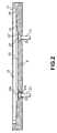
- FIG. 1is a longitudinal sectional view illustrating schematically the epitaxial wafer production apparatus in accordance with the present application
- FIG. 2is a longitudinal sectional view illustrating schematically a susceptor
- FIG. 3is a perspective view of the front surface side of the susceptor of the first embodiment
- FIG. 4is a perspective view of the rear surface side of the susceptor of the first embodiment
- FIG. 5is a plan view of the susceptor of the first embodiment
- FIG. 6is a bottom view of the susceptor of the first embodiment
- FIG. 7is a cross-sectional view of the susceptor shown in FIG. 5 along B-B′;
- FIG. 8is a perspective view of the front surface side of the susceptor of the third embodiment.
- FIG. 9is a perspective view of the rear surface side of the susceptor of the third embodiment.
- FIG. 10is a plan view of the susceptor of the third embodiment
- FIG. 11is a bottom view of the susceptor of the third embodiment
- FIG. 12Ais a cross-sectional view of the susceptor shown in FIG. 10 along A-A′;
- FIG. 12Bis a cross-sectional view of the susceptor shown in FIG. 10 along C-C′;
- FIG. 13is a longitudinal sectional view illustrating another example of the epitaxial wafer production apparatus in accordance with the present application.
- FIG. 14is a plan view of the susceptor of the second embodiment
- FIG. 15is a cross-sectional view of the susceptor shown in FIG. 14 along D-D′;
- FIG. 16is a longitudinal sectional view illustrating schematically the conventional susceptor.
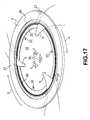
- FIG. 17is a perspective view of the front surface side of the susceptor of the fourth embodiment.
- FIG. 1is a longitudinal sectional view illustrating a schematic structure of an epitaxial wafer production apparatus 1 in accordance with the present invention.
- the schematic structure itself of the epitaxial wafer production apparatus 1 in accordance with the present inventionis almost identical to that of the epitaxial wafer production apparatus explained with reference to the prior art technology. Therefore, the explanation will be conducted by using the same figure.
- the structure of the chamber 2is mainly described, and specific drawing of a rotary drive mechanism is omitted.
- a cylindrical base ring 3is sandwiched from above and below by a disk-like upper window 5 and a saucer-like lower window 6 , and the internal closed space forms a reaction furnace.
- Transparent quartzis used for the upper window 5 and lower window 6 so as to avoid shielding of the light from the heat sources.
- the reaction furnace formed inside the chamber 2is divided into an upper chamber 7 a which is the space above the wafer 12 and a lower chamber 7 b which is the space below the wafer 12 .
- each of the upper and lower heat sources 8 , 9is composed of a plurality of halogen lamps (IR lamps).
- a susceptor 4 for supporting in the upper part thereof the wafer 12is accommodated in the chamber 2 .
- the susceptor 4has a round disk-like shape, if viewed from above, the diameter thereof being larger than that of the wafer 12 .
- a round concave wafer pocket 13 for accommodating the wafer 12is provided in the upper surface of the susceptor 4 .
- the susceptor 4is prepared by coating a silicon carbide SiC film on a carbon C substrate and plays a role of a liner base maintaining a uniform temperature over the entire wafer 12 when the wafer 12 is heated.
- the susceptor 4has a thickness and a thermal capacity several times those of the wafer 12 .
- the susceptor 4rotates about the vertical axis as a rotation center in the plane parallel to the sheet plate of the wafer 12 in the course of the epitaxial layer growing operation.
- the center of the wafer pocket 13 provided in the susceptor 4obviously coincides with the rotation center of the susceptor 4 .
- the three susceptor arms 15are arranged radially so as to form an angle of 120° therebetween, if viewed from above, and the upward protrusions provided on the distal ends of the susceptor arms 15 are abutted against the lower surface of the susceptor 4 and support the susceptor 4 .
- the susceptor support shaft 14is disposed vertically in the position such that the axial center thereof coincides with the center of the round disk of the susceptor 4 , and the susceptor 4 is rotated by the rotation of the susceptor support shaft 14 .
- the rotationis provided to the susceptor support shaft 14 from a rotary drive mechanism (not shown in the figures).
- Transparent quartzis used for the susceptor support shaft 14 and the susceptor arms 15 so as to avoid shielding of the light from the heat source 9 .
- a longitudinal section of the susceptor 4is shown schematically in FIG. 2.
- the wafer pocket 13 of the susceptor 4is composed of a plurality of step-like portions and a tapered surface, as described hereinbelow.
- a round disk-like member with a diameter of 350-400 mm and a thickness of 3-6 mmis used as the susceptor 4 .
- a first step-like portion 30 in the form of a round concave portionis provided in the position at a distance of 20-40 mm from the outer periphery of the upper surface of the susceptor 4 toward the center.
- the first step-like portion 30is a round flat surface provided in a position 0.4-0.7 mm below the upper surface of the susceptor 4 and is a horizontal surface, that is, parallel to the upper surface of the susceptor 4 .
- a tapered surface 31 with a gentle inclinationis provided starting from the position at a distance of 5-6 mm from the outer periphery of the first step-like portion 30 toward the center.
- the tapered surface 31starts from a position about 0.1 mm further below the first step-like portion 30 and forms a funnel shape with a very gentle slope toward the center, the gradient of descending being about 0.1 mm over a distance of 24-27 mm.
- a second step-like portion 32 in the form of a round concave portionis provided further toward the center from the tapered surface 31 .
- the second step-like portion 32is a round flat surface provided in a position of about 0.3 mm below the tapered surface 31 and is a horizontal surface, that is, parallel to the upper surface of the susceptor 4 .
- Three through orifices 22are provided in the second step-like portion 32 , and dish-like orifices 22 ′ expanding upward are formed above each through orifice 22 .
- the lift pin 23 for supporting a waferis inserted in each of the three through orifices 22 .
- the diameter of the through orifice 22is larger than the diameter of the lift pin 23 and the orifice is formed so as to have a size such that the lift pin 23 moves up and down with respect to the susceptor 4 , without coming into contact therewith
- the lift pins 23are composed of quartz, silicon Si, silicon carbide SiC, or quartz coated with a thin film of silicon Si or silicon carbide SiC.
- the lift pin 23has a round rod- or tube-like shape and a head portion 24 is provided at the upper end thereof, the head portion having a tapered surface 24 b on the lower outer periphery thereof which corresponds to the dish-like orifice 22 ′.
- the taper angle of the tapered surface 24 b of the head portion 24matches the taper angle of the tapered surface of the dish-like orifice 22 ′.
- the head portion 24provides excellent sealing with respect to the inner wall of the dish-like orifice 22 ′, thereby preventing leakage of the raw material gas through the space between the lift pin 23 and the inner wall of the through orifice 22 .
- the upper part 24 a of the head portion 24has a conical shape with an obtuse vertical angle, thereby greatly reducing the contact surface area when supporting the rear surface of the wafer. As a result, the occurrence of damage of the rear surface of the wafer by the lift pins 23 is prevented.
- the head portion 24 of the lift pin 23mates with the inner wall of the dish-like orifice 22 ′ of the susceptor 4 , and when the lift pin 23 is lowered, it hangs down vertically under gravity. In this state, the upper part 24 a of the head portion 24 does not protrude from the upper surface of the second step-like portion 32 .
- the lift pin 23hangs down from the susceptor 4 and the body thereof is inserted into the through orifice provided in the susceptor arm 15 . Because the lift pin 23 is an independent unit structure separated from the below-described lift arm 16 , when the susceptor 4 rotates, the lift pin 23 also rotates together with the susceptor 4 , but the lift arm 16 maintains a stationary state. Because the body of the lift pin 23 is inserted into the through orifice provided in the susceptor arm 15 , when the susceptor 4 rotates, the lift pin 23 can be prevented from being tilted by a centrifugal force.
- a cylindrical lift shaft 17 with an inner diameter allowing the shaft to slide with respect to the susceptor support shaft 14is provided on the outer periphery of the susceptor support shaft 14 .
- Three lift arms 16 arranged radially so as to form an angle of 120° therebetween, if viewed from above,are provided at the upper end of the lift shaft 17 .
- a heat-sink ring 19 in the form of a round ring with a thickness almost equal to that of the susceptor 4is fixedly arranged so as to surround the susceptor 4 on the outer periphery of the susceptor 4 .
- the inner peripheral surface of the heat-sink ring 19is disposed at a certain distance from the outer peripheral surface of the susceptor 4 so as to prevent contact therebetween.
- the susceptor 4can rotate independently from the heat-sink ring 19 .
- the heat-sink ring 19is fabricated by coating a film of silicon carbide SiC on a carbon C substrate and serves to prevent rapid temperature changes accompanying changes in thermal capacity in the outer peripheral portion of the susceptor 4 .
- Providing the heat-sink ring 19 around the susceptor 4 in the above-described mannermakes it possible to heat the susceptor 4 almost uniformly from the central portion to the outer peripheral portion thereof.
- a gas supply vent 10 a and a gas discharge vent 11are provided in the base ring 3 .
- the carrier gas containing the raw material gasis supplied through the gas supply vent 10 a shown on the left side and discharged from the gas discharge vent 11 shown on he right side of this figure.
- the raw material gas and the carrier gasare supplied into the chamber 2 through the gas supply vent 10 a from the gas supply unit (not shown in the figure) provided outside the chamber.
- the gas supply vent 10 ahas an opening above the heat-sink ring 19 in the inner peripheral surface of the base ring 3 and supplies hydrogen gas H 2 or hydrogen gas containing the raw material gas into the upper chamber 7 a .
- the raw material gasis prepared by adding a dopant gas of diborane (P type) or phosphine (N type) to a chlorosilane-type silicon source gas such as trichlorosilane SiHCl 3 or dichlorosilane SiH 2 Cl 2 . Those gases are introduced into the upper chamber 7 a together with hydrogen gas H 2 which is the carrier gas.
- the lower supply vent 10 bis provided separately from the gas supply vent 10 a , and hydrogen gas H 2 is supplied into the lower chamber 7 b through the lower supply vent 10 b from a gas supply unit (not shown in the figure) provided outside the chamber.
- the lower supply vent 10 bhas an opening below the heat-sink ring 19 in the inner peripheral surface of the base ring 3 and supplies hydrogen gas H 2 into the lower chamber 7 b.
- the gas discharge vent 11has two openings, above and below the heat-sink ring 19 , in the inner peripheral surface of the base ring 3 and discharges the gas from both the upper chamber 7 a and the lower chamber 7 b to the outside of the chamber 2 .
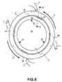
- FIG. 3is a perspective view of the front surface side of the susceptor 4 .
- FIG. 4is a perspective view of the rear surface side of the susceptor 4 .
- the susceptor 4is provided with four notches passing from the rear surface side of the susceptor 4 and reaching the middle of the susceptor 4 .
- Each notchhas a rectangular opening in the outer peripheral surface of the susceptor 4 .
- the notches disposed in the positions symmetrical with respect to the center of the susceptor 4form pairs.
- two gas inlet notches 25 and two gas discharge notches 26are formed.
- FIG. 1is a perspective view of the front surface side of the susceptor 4 .
- FIG. 4is a perspective view of the rear surface side of the susceptor 4 .
- the susceptor 4is provided with four notches passing from the rear surface side of the susceptor 4 and reaching the middle of the susceptor 4 .
- Each notchhas a rectangular opening in the outer peripheral surface of the susceptor 4
- the gas inlet notches 25 and gas discharge notches 26form wide grooves which draw gentle curves, if viewed from the rear surface side of the susceptor 4 .
- the cross-sectional shape of the groovepreferably narrows from the outer periphery of the susceptor 4 toward the central part of the susceptor 4 , but also may be constant.
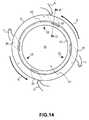
- FIG. 5is a plan view of the susceptor 4
- FIG. 6is a bottom view of the susceptor 4 .
- the gas inlet notches 25are formed so as to whirl clockwise toward the center
- the gas discharge notches 26are formed so as to whirl clockwise toward the outer side.
- FIG. 7is a cross-sectional view along B-B′ in FIG. 5. Because the gas inlet notches 25 and gas discharge notches 26 have identical cross-sectional shape, only the cross-sectional shape of the gas inlet notches 25 will be explained herein. As shown in FIG. 7, the gas inlet notches 25 form grooves in the direction toward the center from the outer peripheral surface of the susceptor 4 to the initiation position of the tapered surface 31 . Further, they pass through the susceptor 4 at an inclination of 10-45° and form an opening in the tapered surface 31 . More preferably, they pass through the susceptor 4 at an angle of 20°. As a result, a groove is formed in the rear surface of the susceptor 4 , this groove drawing a curve from the outer peripheral surface of the susceptor 4 toward the center thereof and penetrates into the wafer pocket 13 by entering through the tapered surface 31 .
- the susceptor 4rotates counterclockwise, if viewed from above.
- the carrier gas present inside the lower chamber 7 bflows into the wafer pocket 13 from the gas inlet notches 25 of the susceptor 4 , as shown by arrows b, and the gas present inside the wafer pocket 13 is discharged from the gas discharge notches 26 , as shown by arrows c.
- the carrier gasflows in from the rear surface side of the susceptor 4 through the gas inlet notches 25 , circulates inside the wafer pocket 13 , and is discharged to the rear surface side of the susceptor 4 through the gas discharge notches 26 .
- the atmosphere containing dopant species which diffuses from the rear source of the wafer in the process of epitaxial growthcan be discharged from the wafer pocket 13 , without causing a large quantity of the raw material gas to flow from the front surface side of the susceptor 4 to under the susceptor 4 .
- the gas present inside the wafer pocket 13is forcibly discharged by using the rotation of the susceptor 4 during epitaxial growth, the atmosphere containing the dopant species and filling the wafer pocket 13 can be more effectively prevented from overflowing to the front surface of the wafer 12 .
- a configurationwas used in which the gas present in the wafer pocket 13 was forcibly discharged by forming the gas inlet notches 25 and the gas discharge notches 26 as curved grooves.
- the effect of discharging the gas present in the wafer pocket 13can be also demonstrated even when the notches are not in the form of a curved groove.
- the gas inlet notches 25 and the gas discharge notches 26have symmetrical shapes. Therefore, the gas present in the wafer pocket 13 can be also forcibly discharged when the susceptor 4 is rotated either in the clockwise direction or in the counterclockwise direction. For example, when the susceptor is rotated in the direction (clockwise direction) opposite to the counterclockwise direction shown in FIG. 5, the gas inlet notches 25 function for gas discharge, and the gas discharge notches 26 function for gas inlet.
- gas inlet notches 25 and the gas discharge notches 26passed through from the rear surface side of the susceptor 4 to the tapered surface 31 .
- notches of one type of both typesmay also pass through to the second step-like portion 32 .
- the number of the gas inlet notches 25 and the gas discharge notches 26can vary depending on the design and at least one of them may be used.
- FIG. 14 and FIG. 15illustrate another example.
- FIG. 14is a plan view of the susceptor 4 viewed from the upper surface.
- FIG. 15is a cross section along D-D′. Because the shape of the rear surface of the wafer is identical to that of the first embodiment, the explanation will be conducted with reference to FIG. 4.
- the susceptor 4similarly to the first embodiment, comprises four notches passing from the rear surface side of the susceptor 4 to the middle of the susceptor 4 in the thickness direction, each notch having a rectangular opening in the outer peripheral surface of the susceptor 4 .
- the notches disposed in the positions symmetrical with respect to the center of the susceptor 4form pairs.
- the gas inlet notches 25 and gas discharge notches 26form wide grooves which draw gentle curves, if viewed from the rear surface side of the susceptor 4 .
- the cross-sectional shape of the groovepreferably narrows from the outer periphery of the susceptor 4 toward the central part of the susceptor 4 , but also may be constant.
- the gas inlet notches 25are formed so as to whirl clockwise toward the center, and the gas discharge notches 26 are formed so as to whirl clockwise toward the outer side.
- the susceptor 4 of the present embodimentcomprises a surface 52 for carrying the wafer 12 and a gas sweeping step-like portion 51 formed in the outer peripheral portion of the surface 52 .
- the surface 52is obtained by removing part of the upper surface of the susceptor 4 so as to obtain a round concave shape approximately matching that of the wafer 12 .
- the gas sweeping step-like portion 51is further lowered toward the rear surface side of the wafer from the surface 52 and is a flat surface of a round ring shape provided on the outer periphery of the surface 52 .
- the wafer 12 shown by a two-dot-dash lineis placed on the surface 52 formed on the inner side of the gas sweeping step-like portion 51 and is disposed so that the outer peripheral portion thereof covers the gas sweeping step-like portion 51 from above. As a result, a round ring-like space 53 is formed between the wafer 12 and the gas sweeping step-like portion 51 .
- the surface 52may be subjected to the so-called knurling process forming mesh-like fine shallow grooves.
- the gas inlet notches 25 and the gas discharge notches 26 in the present embodimentwill be described below. Because the gas inlet notches 25 and gas discharge notches 26 have identical cross-sectional shape, only the cross-sectional shape of the gas inlet notches 25 will be explained herein. As shown in FIG. 15, the gas inlet notches 25 form grooves in the direction toward the center from the outer peripheral surface of the susceptor 4 to the initiation position of the gas sweeping portion 51 . Further, they pass through the susceptor 4 at an inclination of 10-45° and form an opening in the gas sweeping portion 51 . More preferably, they pass through the susceptor 4 at an angle of 20°.
- the susceptor 4rotates counterclockwise, if viewed from above.
- the carrier gas present inside the lower chamber 7 b of the susceptor 4flows into the gas sweeping portion 51 from the gas inlet notches 25 of the susceptor 4 , as shown by arrows b, and is discharged from the gas discharge notches 26 , as shown by arrows c.
- the carrier gasflows in from the rear surface side of the susceptor 4 through the gas inlet notches 25 , circulates inside the round ring-like space 53 , and is discharged to the rear surface side of the susceptor 4 through the gas discharge notches 26 .
- the atmosphere containing the dopant species and filling the wafer pocket 13can be discharged without causing a large quantity of the raw material gas to flow from the front surface side of the susceptor 4 to under the susceptor 4 .
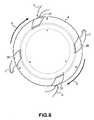
- FIG. 8is a perspective view of the front surface side of the susceptor 4 .
- FIG. 9is a perspective view of the rear surface side of the susceptor 4 .
- the susceptor 4comprises three notches passing from the rear surface side of the susceptor 4 to the middle of the susceptor 4 in the thickness direction.
- Each notchis a gas inlet notch 27 having a rectangular opening in the outer peripheral surface of the susceptor 4 .
- the gas inlet notches 27form wide grooves which draw gentle curves, if viewed from the rear surface side of the susceptor 4 .
- the cross-sectional shape of the groovepreferably narrows from the outer periphery of the susceptor 4 toward the central part of the susceptor 4 , but also may be constant.
- FIG. 10is a plan view of the susceptor 4
- FIG. 11is a bottom view of the susceptor 4 .
- the gas inlet notches 27are formed so as to whirl counterclockwise toward the center.
- the gas inlet notches 27are provided in the positions obtained by dividing a circle equidistantly, so as to form an angle of 120° therebetween with respect to the center of the susceptor 4 .
- FIG. 12Ais a cross-sectional view along A-A′ in FIG. 10.
- the gas inlet notches 27form grooves in the direction toward the center from the outer peripheral surface of the susceptor 4 to the initiation position of the tapered surface 31 . Further, they pass through the susceptor 4 at an inclination of 10-45° and form an opening in the tapered surface 31 . More preferably, they pass through the susceptor 4 at an angle of 20°.
- a grooveis formed in the rear surface of the susceptor 4 , this groove drawing a curve from the outer peripheral surface of the susceptor 4 toward the center thereof and penetrates into the wafer pocket 13 by entering through the tapered surface 31 .
- the susceptor 4 of the present embodimentcomprises gas discharge openings 28 passing through the susceptor 4 from the front surface side to the rear surface side thereof in the flat surface of the second step-like portion 32 , that is, close to the central part of the susceptor.
- FIG. 12Bis a cross-sectional view along C-C′ in FIG. 10.
- the gas discharge opening 28has an opening on the upper surface of the second step-like portion 32 of the wafer pocket 13 , passes through the susceptor 4 at an inclination of 10-45° and again forms an opening on the rear surface of the susceptor 4 . More preferably, it passes through the susceptor 4 at an angle of 20°.
- the gas discharge opening 28 shown in FIG. 10has a quadrangular cross-sectional shape, but the cross-sectional shape does not need to be rectangular and may be round or triangular.
- the susceptor 4rotates clockwise, if viewed from above.
- the carrier gas present inside the lower chamber 7 b of the susceptor 4flows into the wafer pocket 13 from the gas inlet notches 27 , as shown by arrows b, and the gas present inside the wafer pocket 13 is discharged from the gas discharge openings 28 , as shown by arrows c.
- the carrier gasflows in from the rear surface side of the susceptor 4 through the gas inlet notches 27 , circulates inside the wafer pocket 13 , and is discharged to the rear surface side of the susceptor 4 through the gas discharge openings 28 .
- the atmosphere containing the dopant species and filling the wafer pocket 13can be discharged without causing a large quantity of the raw material gas to flow from the front surface side of the susceptor 4 to under the susceptor 4 .
- the atmosphere containing the dopant species and filling the wafer pocket 13can be more effectively prevented from overflowing to the front surface of the wafer 12 .
- gas inlet notches 27passed through from the rear surface side of the susceptor 4 to the tapered surface 31 , but they may also pass through to the second step-like portion 32 . Further, the number of the gas inlet notches 27 can vary depending on the design and at least one of them may be used.
- the configurationdoes not need to be as described in the first to third embodiments, in particular, with the shape of the wafer pocket 13 being a combination of a step-like portion and a tapered surface, and a configuration comprising only a step-like portion or only a tapered surface, a configuration in which mesh-like fine shallow grooves called knurls are formed and the wafer is supported by contact with a plurality of protrusions, or a configuration in which the surface roughness of silicon carbide coated on the surface is much higher than that of the rear surface of the wafer may be used.
- the present inventionis applicable to any of those configurations and can be used in all the configurations in which a gas is taken from the side or rear surface of the susceptor 4 into the wafer pocket 13 and again discharged from the side or rear surface of the susceptor 4 .
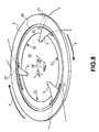
- FIG. 17is a perspective view of the front surface side of a susceptor 4 .
- a specific feature of the susceptor 4 of the present embodimentis that a gas escape groove 20 is provided therein, in particular, as shown by a solid line in FIG. 17.
- the gas escape groove 20is a round ring-like shallow groove formed in a tapered surface 31 , this groove being formed so as to link together the openings of the gas inlet notches 27 on the side of a wafer pocket 13 .
- the gas escape groove 20may have a width of 3.0 mm and a depth of about 1.5 mm, but it goes without saying that the groove width may be more than 3.0 mm and the groove depth may be more than 1.5 mm. From the standpoint of increasing the gas discharge efficiency, it is desired that the groove width be no less than 1.0 mm and the groove depth be no less than 0.5 mm.
- the gas escape groove 20 of the present embodimentcan be also formed to have the shape of a round ring linking together the openings of the gas inlet notches 25 and the gas discharge notches 26 in the above-described first embodiment.
- the gas discharge efficiency in the zone where the groove is presentcan be increased or the uniformity of gas discharge efficiency in the tangential direction of the wafer can be improved.
- the upper and lower heat sources 8 , 9are activated and the susceptor 4 located inside the treatment chamber 2 is heated to the temperature appropriate for the transportation of the wafer.
- the wafer transportation temperatureis preferably about 800° C. and is controlled so as to be maintained within the above-mentioned temperature range, while detecting the temperature of the susceptor 4 located inside the chamber 2 , e.g., with a thermal sensor.
- a carrier gasis introduced from the gas supply vent 10 a and the lower supply vent 10 b , and the upper chamber 7 a and the lower chamber 7 b are filled with the carrier gas.
- the chamber 2has the gas discharge vent 11 on the side opposite the gas supply vent 10 a , and the carrier gas constantly flows from the gas supply vent 10 a and the lower supply vent 10 b toward the gas discharge vent 11 .
- Hydrogen H 2is generally most often used as the carrier gas, and the carrier gas is supplied into the chamber 2 in a normal temperature (room temperature) state.
- the wafer 12is placed into the chamber 2 .
- the wafer 12is sliced from an ingot and formed into a thin round disk, for example, by a polishing process.
- the waferhas a diameter of 300 mm and a thickness of about 0.7-0.75 mm.
- the wafer 12is placed on a quartz hand and the hand is introduced into the chamber 2 .
- the wafer 12is transferred on the lifted lift pins 23 and the lift pins 23 are gradually lowered. As a result, the wafer 12 is fit into the wafer pocket 13 of the susceptor 4 and assumes a state in which no displacement occurs in the left-right direction.
- the upper and lower heat sources 8 , 9are activated and the wafer surface temperature is raised to the temperature (1000-1200° C.) suitable for epitaxial growth. Further, a rotary drive motor is driven in response to a command from a control unit (not shown in the figures) and the susceptor 4 is rotated. Once the rotation of the susceptor 4 has stabilized, a raw material gas is mixed with the carrier gas and the raw material gas is supplied into the upper chamber 7 a via the gas inlet vent 10 a .
- the raw material gasis obtained by adding a dopant gas of diborane (P type) or phosphine (N type) to a chlorosilane-type silicon source gas, mainly such as trichlorosilane SiHCl 3 or dichlorosilane SiH 2 Cl 2 .
- a dopant gas of diborane (P type) or phosphine (N type)to a chlorosilane-type silicon source gas, mainly such as trichlorosilane SiHCl 3 or dichlorosilane SiH 2 Cl 2 .
- the carrier gas containing the raw material gasflows to the front surface of the wafer 12 and an epitaxial layer starts to grow on the front surface of the wafer. Because the wafer 12 is rotated in the horizontal plane in a state in which it is accommodated in the susceptor 4 , an epitaxial layer of an almost uniform thickness grows on the front surface of the wafer 12 . In this process, HCl is produced as a byproduct in the course of silicon epitaxy by a thermal CVD reaction on the front surface of the wafer.
- silicon epitaxyproceeds on the front surface of the wafer, but because a Si—H—Cl atmosphere remains inside the wafer pocket 13 due to an overflow mainly caused by gas diffusion on the rear surface of the wafer, the emission of dopant species from the rear surface of the wafer is initiated in the Si—H—Cl atmosphere.
- the rotation during film formation on the front surface of the waferis used to absorb the carrier gas (hydrogen gas H 2 containing no raw material gas) present inside the lower chamber 7 b from the side surface or rear surface of the susceptor 4 , to cause the circulation thereof inside the wafer pocket 13 , and then to discharge it from the side surface or the rear surface of the susceptor 4 .
- the gasis then discharged to the outside of the chamber from the opening located below the gas discharge vent 11 . Therefore, the retention of the Si—H—Cl atmosphere inside the wafer pocket 13 can be prevented and the effect of emission of the dopant species from the rear surface of the wafer can be suppressed.
- the supply of the raw material gasis terminated, the heat sources 8 , 9 are controlled and the temperature inside the chamber 2 is lowered to the wafer transportation temperature.
- the treated wafer 12is taken out of the chamber 2 .
- the taking-out procedureis a reversed taking-in procedure.
- FIG. 13is a longitudinal sectional view illustrating a schematic structure of the epitaxial wafer production apparatus 40 .
- the schematic structure of the epitaxial wafer production apparatus 40 itselfis almost identical to that of the epitaxial wafer production apparatus 1 explained with reference to FIG. 1. Therefore, identical components will be assigned with the same symbols and the specific explanation thereof will be omitted.
- heavy gas supply means 41 and carrier gas supply means 42are linked to a heavy gas supply vent 45 formed in a base ring 3 .
- a heavy gas source 44is connected to the heavy gas supply means 41 via flow rate adjustment means 43 , and the heavy gas supplied from the heavy gas source 44 is adjusted to the desired supply quantity with the flow rate adjustment means 43 .
- the heavy gas supplied from the heavy gas supply means 41is mixed with the carrier gas supplied from the carrier gas supply means 42 and is supplied from the heavy gas supply vent 45 to the lower chamber 7 b .
- the supply quantities of the gas supplied from the gas supply vent 10 a and the gas supplied from the heavy gas supply vent 45are controlled by a process controller (not shown in the figures).
- the heavy gas supply vent 45supplies the heavy gas from outside the chamber 2 only into the lower chamber 7 b , without intersecting with the gas supply vent 10 a .
- argon gascan be used as the heavy gas.
- the heavy gasis essentially required to be heavier than the carrier gas supplied to the upper chamber 7 a .
- An argon gas tank or a pipe from an argon gas purification plantcan be used as the heavy gas source 44 , and a mass flow controller can be used as the flow rate adjustment means 43 .
- the inside of the lower chamber 7 b of the chamber 2is filled with the heavy gas, e.g., argon gas, supplied from the heavy gas supply vent 45 . Because the heavy gas is heavier than the carrier gas supplied into the upper chamber 7 a , the inside of the lower chamber 7 b is filled with the heavy gas, thereby making it possible to prevent the carrier gas and the raw material gas from flowing into the lower chamber from the upper chamber 7 a . As a result, the atmosphere containing dopant species and filling the wafer pocket 13 can be discharged without causing a large quantity of the raw material gas to flow from the front surface side of the susceptor 4 to under the susceptor 4 . Further, FIG. 13 illustrates an example in which the heavy gas supply vent 45 supplies a mixture of the carrier gas and the heavy gas, but a carrier gas supply vent and a heavy gas supply vent may be also provided independently.
- the heavy gas supply vent 45supplies a mixture of the carrier gas and the heavy gas, but a carrier gas supply vent and a heavy gas supply vent may be also
Landscapes
- Chemical & Material Sciences (AREA)
- Chemical Kinetics & Catalysis (AREA)
- General Chemical & Material Sciences (AREA)
- Engineering & Computer Science (AREA)
- Materials Engineering (AREA)
- Metallurgy (AREA)
- Organic Chemistry (AREA)
- Crystallography & Structural Chemistry (AREA)
- Mechanical Engineering (AREA)
- Chemical Vapour Deposition (AREA)
Abstract
Description
- 1. Field of the Invention[0001]
- The present invention relates to an epitaxial wafer production apparatus, a susceptor structure, and an epitaxial wafer production method for the formation of an epitaxial layer on a wafer, and more particularly to an epitaxial wafer production apparatus, a susceptor structure, and an epitaxial wafer production method capable of suppressing the increase in dopant concentration in the peripheral edge portion of the front surface of the epitaxial wafer.[0002]
- 2. Description of the Related Art[0003]
- A technology is known for the production of a silicon wafer which is free from crystal defects and has the desired resistivity by growing a crystal layer of silicon on the front surface of the wafer. For example, in the case of a wafer with a diameter of 200 mm and a thickness of 0.75 mm, such a silicon crystal layer is an ultra-thin layer with a thickness of about several microns. It is generally called an epitaxial layer, and an apparatus for forming the epitaxial layer called an epitaxial wafer production apparatus. Epitaxial wafer production apparatuses of a single wafer processing type, in which silicon wafers were processed one by one, have been used most often because of high quality of the film produced and easiness of film thickness control.[0004]
- As shown in FIG. 1, in the epitaxial wafer production apparatus of a single wafer processing type, a susceptor[0005]4 (wafer support) supporting one wafer horizontally is usually provided inside a
treatment chamber 2. Further, a lift mechanism for moving awafer 12 up and down with respect to thesusceptor 4 is provided for transporting thewafer 12 on thesusceptor 4. The lift mechanism comprises a plurality oflift pins 23 extending through thesusceptor 4. Thewafer 12 is carried on the upper ends of thoselift pins 23, and thewafer 12 is lifted or lowered by moving thelift pins 23 up and down with respect to thesusceptor 4. With such a lift mechanism, thewafer 12 carried by the hand of a transport arm and into thechamber 2 is moved on thesusceptor 4 or, conversely, transferred from thesusceptor 4 to the hand. - Further, the[0006]
wafer 12 supported on thesusceptor 4 has to be heated at a high temperature to grow an epitaxial film. For this reason,heat sources 8,9 such as a plurality of halogen lamps (IR lamps) are arranged above and below thetreatment chamber 2 to heat thesusceptor 4 and thewafer 12. - The[0007]
susceptor 4 is prepared by coating a silicon carbide SiC film on a carbon C substrate and plays a role of a liner base maintaining a uniform temperature over theentire wafer 12 when thewafer 12 is heated. As shown in FIG. 2, a recess called a wafer pocket, which is larger in size than thewafer 12 and has a depth of about 1-2 mm is formed in the upper surface of thesusceptor 4 to accommodate, for example, a silicon wafer. The inner surface of thewafer pocket 13 has a tapered configuration so as to be in contact only with the outer peripheral portion of the wafer, and measures are taken to minimize the surface contact of thewafer 12 and the inner surface of thewafer pocket 13. An epitaxial layer composed of a silicon thin film is grown on the surface of thewafer 12 by accommodating thewafer 12 inside thewafer pocket 13 and holding thesusceptor 4 in a carrier gas containing a raw material gas at the prescribed temperature. The raw material gas as referred to herein is a silicon source gas and a dopant gas. - A chlorosilane gas such as trichlorosilane SiHCl[0008]3or dichlorosilane SiH2Cl2is usually used as the silicon gas, and diborane (P type) and phosphine (N type) are usually used as the dopant gas. Those gases are introduced into the chamber together with hydrogen H2as a carrier gas, and HCl is produced as a byproduct in the course of silicon epitaxy by a thermal CVD reaction on the front surface of the wafer. Therefore, though silicon epitaxy proceeds on the front surface of the wafer, a Si—H—Cl atmosphere is formed on the rear surface of the wafer by an overflow mainly caused by gas diffusion, and emission of dopant species from the rear surface of the wafer occurs in the Si—H—Cl atmosphere.
- As a result, the atmosphere comprising dopant species and filling the[0009]
wafer pocket 13 overflows onto the front surface of the wafer by diffusion, and the dopant concentration in the gas phase locally increases in the outer edge portion of the front surface of thewafer 12. As a result, an effect can be observed of the dopant concentration in the epitaxial layer being increased in the peripheral edge portion of the front surface of the wafer. - In order to prevent the above-described overflow of the atmosphere comprising dopant species and filling the[0010]
wafer pocket 13 onto the front surface of the wafer, in accordance with the invention described in Japanese Patent Application Laid-open No. 10-223545, ahole 50 passing to the rear surface of thesusceptor 4 is provided in the outermost peripheral portion of thewafer pocket 13, as shown in FIG. 16. Thus providing ahole 50 passing from the front surface to the rear surface of thesusceptor 4 in the outermost peripheral portion of thewafer pocket 13 makes it possible to prevent the overflow of the atmosphere comprising dopant species and filling thewafer pocket 13 onto the front surface of thewafer 12 because the carrier gas containing the raw material gas and flowing on the front surface side of thesusceptor 4 outflows to under thesusceptor 4 through thehole 50. - According to the invention described in Japanese Patent Application Laid-open No. 10-223545, when the gas is caused to outflow from the front surface side of the[0011]
susceptor 4 to under thesusceptor 4, the raw material gas such as trichlorosilane SiHCl3or dichlorosilane SiH2Cl2, which has a high reactivity, and HCl and amorphous Si obtained by decomposition in a gas phase flow out in a large amount together with the carrier gas into alower chamber 7b. - Referring to FIG. 1, it is clear that the[0012]
lower chamber 7bcomprises a rotary drive mechanism, a lift mechanism, and a transport arm advancement channel for thewafer 12 and is very difficult to clean. The above-described introduction of the raw material gas and decomposition products results in a significant increase in maintenance time and causes a decrease in productivity. Further, the increase in maintenance cost also cannot be ignored. - Furthermore, because heating is also conducted by the[0013]
heat source 9 from the side of thelower chamber 7b, contamination of the chamber inner wall degrades the uniformity and reproducibility of heating of thesusceptor 4 and also causes a spread in the wafer quality. - The invention of the present application was created to resolve the above-described problems, and it is an object of the present invention to provide an epitaxial wafer production apparatus and a susceptor structure capable of discharging the atmosphere containing dopant species and filling the wafer pocket, without causing the flow of a large quantity of the raw material gas from the front surface side of the susceptor to under the susceptor.[0014]
- Further, it is another object of the invention of the present application to provide an epitaxial wafer production apparatus and an epitaxial wafer production method which make it difficult for the raw material gas to flow from the front surface side of the susceptor to under the susceptor.[0015]
- In order to attain the above-described objects, a first aspect of the invention provides a susceptor of an approximately round disk shape, having a concave wafer pocket on a front surface thereof for accommodating a wafer, comprising: a gas supply channel passing through from a side surface or a rear surface of the susceptor to the wafer pocket; and a gas discharge channel passing through from the wafer pocket to the side surface or the rear surface of the susceptor.[0016]
- A second aspect of the invention provides the susceptor according to the first aspect, wherein the gas supply channel has a shape adapted to supply a gas into the wafer pocket as the susceptor rotates; and the gas discharge channel has a shape adapted to discharge the gas present in the wafer pocket as the susceptor rotates.[0017]
- A third aspect of the provides an epitaxial wafer production apparatus comprising: a chamber having a gas supply vent and a gas discharge vent; a susceptor of an approximately round disk shape, which is disposed inside the chamber and comprises a concave wafer pocket on the front surface thereof for accommodating a wafer, a gas supply channel passing through from a side surface or a rear surface to the wafer pocket, and a gas discharge channel passing through from the wafer pocket to the side surface or the rear surface; support means for supporting the susceptor; and heating means for heating the susceptor and the wafer inside the chamber.[0018]
- A fourth aspect of the invention provides the epitaxial wafer production apparatus according to the third aspect, comprising a gas supply vent for supplying a carrier gas containing a raw material gas only to above the susceptor located inside the chamber.[0019]
- A fifth aspect of the invention provides an epitaxial wafer production apparatus comprising: a chamber; a susceptor disposed inside the chamber and comprising a concave wafer pocket on a front surface thereof for accommodating a wafer; support means for supporting the susceptor; and heating means for heating the susceptor and the wafer inside the chamber, wherein the apparatus further comprises: a gas supply vent for supplying a carrier gas containing a raw material gas to above the susceptor located inside the chamber; and a heavy gas supply vent for supplying a gas which is heavier than the carrier gas to under the susceptor located inside the chamber.[0020]
- A sixth aspect of the invention provides a method for producing an epitaxial wafer, comprising the steps of placing a wafer into a concave wafer pocket formed on a front surface of a susceptor disposed inside a chamber; supplying a gas from under the susceptor into the wafer pocket; discharging a gas present inside the wafer pocket from under the susceptor; and heating the susceptor and the wafer inside the chamber.[0021]
- A seventh aspect of the invention provides a method for producing an epitaxial wafer, comprising the steps of placing a wafer onto a susceptor disposed inside a chamber; supplying a carrier gas containing a raw material gas to above the susceptor inside the chamber and supplying a gas heavier than the carrier gas to under the susceptor; and heating the susceptor and the wafer inside the chamber.[0022]
- With the susceptor structure of the present invention, the atmosphere containing dopant species and filling the wafer pocket can be discharged without causing a large quantity of the raw material gas to flow from the front surface side of the susceptor to under the susceptor.[0023]
- Further, with the susceptor structure of the present application, because the gas present inside the wafer pocket is forcibly discharged by using the rotation of the susceptor during epitaxial growth, the atmosphere containing the dopant species and filling the wafer pocket can be more effectively prevented from overflowing to the front surface of the wafer.[0024]
- Furthermore, forming the gas inlet notches and the gas discharge notches so that they have symmetrical shapes makes it possible to discharge forcibly the gas present in the wafer pocket when the susceptor is rotated either in the clockwise direction or in the counterclockwise direction.[0025]
- With the epitaxial wafer production apparatus of the present application, supplying into the lower chamber a gas heavier than the carrier gas supplied into the upper chamber makes it possible to fill the lower chamber with the heavy gas and to prevent the carrier gas and the raw material gas from flowing into the lower chamber from the upper chamber. As a result, the atmosphere containing dopant species and filling the wafer pocket can be discharged without causing a large quantity of the raw material gas to flow from the front surface side of the susceptor to under the susceptor.[0026]
- FIG. 1 is a longitudinal sectional view illustrating schematically the epitaxial wafer production apparatus in accordance with the present application;[0027]
- FIG. 2 is a longitudinal sectional view illustrating schematically a susceptor;[0028]
- FIG. 3 is a perspective view of the front surface side of the susceptor of the first embodiment;[0029]
- FIG. 4 is a perspective view of the rear surface side of the susceptor of the first embodiment;[0030]
- FIG. 5 is a plan view of the susceptor of the first embodiment;[0031]
- FIG. 6 is a bottom view of the susceptor of the first embodiment;[0032]
- FIG. 7 is a cross-sectional view of the susceptor shown in FIG. 5 along B-B′;[0033]
- FIG. 8 is a perspective view of the front surface side of the susceptor of the third embodiment;[0034]
- FIG. 9 is a perspective view of the rear surface side of the susceptor of the third embodiment;[0035]
- FIG. 10 is a plan view of the susceptor of the third embodiment;[0036]
- FIG. 11 is a bottom view of the susceptor of the third embodiment;[0037]
- FIG. 12A is a cross-sectional view of the susceptor shown in FIG. 10 along A-A′;[0038]
- FIG. 12B is a cross-sectional view of the susceptor shown in FIG. 10 along C-C′;[0039]
- FIG. 13 is a longitudinal sectional view illustrating another example of the epitaxial wafer production apparatus in accordance with the present application;[0040]
- FIG. 14 is a plan view of the susceptor of the second embodiment;[0041]
- FIG. 15 is a cross-sectional view of the susceptor shown in FIG. 14 along D-D′;[0042]
- FIG. 16 is a longitudinal sectional view illustrating schematically the conventional susceptor; and[0043]
- FIG. 17 is a perspective view of the front surface side of the susceptor of the fourth embodiment.[0044]
- The preferred embodiments of the invention of the present application will be described hereinbelow in greater detail based on FIGS.[0045]1-15 and FIG. 17.
- [Explanation of the Entire Apparatus][0046]
- FIG. 1 is a longitudinal sectional view illustrating a schematic structure of an epitaxial[0047]
wafer production apparatus 1 in accordance with the present invention. The schematic structure itself of the epitaxialwafer production apparatus 1 in accordance with the present invention is almost identical to that of the epitaxial wafer production apparatus explained with reference to the prior art technology. Therefore, the explanation will be conducted by using the same figure. In the figure, the structure of thechamber 2 is mainly described, and specific drawing of a rotary drive mechanism is omitted. - In the[0048]
chamber 2, a cylindrical base ring3 is sandwiched from above and below by a disk-likeupper window 5 and a saucer-like lower window6, and the internal closed space forms a reaction furnace. Transparent quartz is used for theupper window 5 and lower window6 so as to avoid shielding of the light from the heat sources. The reaction furnace formed inside thechamber 2 is divided into anupper chamber 7awhich is the space above thewafer 12 and alower chamber 7bwhich is the space below thewafer 12. - Further, the[0049]
heat sources 8,9 for heating the reaction furnace are provided above and below thechamber 2. In the present embodiment, each of the upper andlower heat sources 8,9 is composed of a plurality of halogen lamps (IR lamps). - A[0050]
susceptor 4 for supporting in the upper part thereof thewafer 12 is accommodated in thechamber 2. Thesusceptor 4 has a round disk-like shape, if viewed from above, the diameter thereof being larger than that of thewafer 12. A roundconcave wafer pocket 13 for accommodating thewafer 12 is provided in the upper surface of thesusceptor 4. In the present example, thesusceptor 4 is prepared by coating a silicon carbide SiC film on a carbon C substrate and plays a role of a liner base maintaining a uniform temperature over theentire wafer 12 when thewafer 12 is heated. For this purpose, thesusceptor 4 has a thickness and a thermal capacity several times those of thewafer 12. - In order to form a homogeneous epitaxial layer on the upper surface of the[0051]
wafer 12, thesusceptor 4 rotates about the vertical axis as a rotation center in the plane parallel to the sheet plate of thewafer 12 in the course of the epitaxial layer growing operation. The center of thewafer pocket 13 provided in thesusceptor 4 obviously coincides with the rotation center of thesusceptor 4. - A[0052]
susceptor support shaft 14 in the shape of a cylindrical rod or tube, which serves as a rotation shaft of thesusceptor 4, is disposed vertically below thesusceptor 4, and threesusceptor arms 15 supporting thesusceptor 4 horizontally are provided above thesusceptor support shaft 14. The three susceptorarms 15 are arranged radially so as to form an angle of 120° therebetween, if viewed from above, and the upward protrusions provided on the distal ends of thesusceptor arms 15 are abutted against the lower surface of thesusceptor 4 and support thesusceptor 4. - The[0053]
susceptor support shaft 14 is disposed vertically in the position such that the axial center thereof coincides with the center of the round disk of thesusceptor 4, and thesusceptor 4 is rotated by the rotation of thesusceptor support shaft 14. The rotation is provided to thesusceptor support shaft 14 from a rotary drive mechanism (not shown in the figures). Transparent quartz is used for thesusceptor support shaft 14 and thesusceptor arms 15 so as to avoid shielding of the light from theheat source 9. - A longitudinal section of the[0054]
susceptor 4 is shown schematically in FIG. 2. Thewafer pocket 13 of thesusceptor 4 is composed of a plurality of step-like portions and a tapered surface, as described hereinbelow. For example, in the apparatus for epitaxial growth of wafers with a diameter of 300 mm, a round disk-like member with a diameter of 350-400 mm and a thickness of 3-6 mm is used as thesusceptor 4. - A first step-[0055]
like portion 30 in the form of a round concave portion is provided in the position at a distance of 20-40 mm from the outer periphery of the upper surface of thesusceptor 4 toward the center. The first step-like portion 30 is a round flat surface provided in a position 0.4-0.7 mm below the upper surface of thesusceptor 4 and is a horizontal surface, that is, parallel to the upper surface of thesusceptor 4. - Furthermore, a[0056]
tapered surface 31 with a gentle inclination is provided starting from the position at a distance of 5-6 mm from the outer periphery of the first step-like portion 30 toward the center. The taperedsurface 31 starts from a position about 0.1 mm further below the first step-like portion 30 and forms a funnel shape with a very gentle slope toward the center, the gradient of descending being about 0.1 mm over a distance of 24-27 mm. - A second step-[0057]
like portion 32 in the form of a round concave portion is provided further toward the center from the taperedsurface 31. The second step-like portion 32 is a round flat surface provided in a position of about 0.3 mm below the taperedsurface 31 and is a horizontal surface, that is, parallel to the upper surface of thesusceptor 4. - Three through orifices[0058]22 (only two orifices are shown in FIG. 2, for convenience of explanation) are provided in the second step-
like portion 32, and dish-like orifices 22′ expanding upward are formed above each throughorifice 22. Thelift pin 23 for supporting a wafer is inserted in each of the three throughorifices 22. The diameter of thethrough orifice 22 is larger than the diameter of thelift pin 23 and the orifice is formed so as to have a size such that thelift pin 23 moves up and down with respect to thesusceptor 4, without coming into contact therewith The lift pins23 are composed of quartz, silicon Si, silicon carbide SiC, or quartz coated with a thin film of silicon Si or silicon carbide SiC. Thelift pin 23 has a round rod- or tube-like shape and ahead portion 24 is provided at the upper end thereof, the head portion having a taperedsurface 24bon the lower outer periphery thereof which corresponds to the dish-like orifice 22′. The taper angle of the taperedsurface 24bof thehead portion 24 matches the taper angle of the tapered surface of the dish-like orifice 22′. As a result, thehead portion 24 provides excellent sealing with respect to the inner wall of the dish-like orifice 22′, thereby preventing leakage of the raw material gas through the space between thelift pin 23 and the inner wall of thethrough orifice 22. - The[0059]
upper part 24aof thehead portion 24 has a conical shape with an obtuse vertical angle, thereby greatly reducing the contact surface area when supporting the rear surface of the wafer. As a result, the occurrence of damage of the rear surface of the wafer by the lift pins23 is prevented. Thehead portion 24 of thelift pin 23 mates with the inner wall of the dish-like orifice 22′ of thesusceptor 4, and when thelift pin 23 is lowered, it hangs down vertically under gravity. In this state, theupper part 24aof thehead portion 24 does not protrude from the upper surface of the second step-like portion 32. - As shown in FIG. 1, the[0060]
lift pin 23 hangs down from thesusceptor 4 and the body thereof is inserted into the through orifice provided in thesusceptor arm 15. Because thelift pin 23 is an independent unit structure separated from the below-describedlift arm 16, when thesusceptor 4 rotates, thelift pin 23 also rotates together with thesusceptor 4, but thelift arm 16 maintains a stationary state. Because the body of thelift pin 23 is inserted into the through orifice provided in thesusceptor arm 15, when thesusceptor 4 rotates, thelift pin 23 can be prevented from being tilted by a centrifugal force. - A[0061]
cylindrical lift shaft 17 with an inner diameter allowing the shaft to slide with respect to thesusceptor support shaft 14 is provided on the outer periphery of thesusceptor support shaft 14. Threelift arms 16 arranged radially so as to form an angle of 120° therebetween, if viewed from above, are provided at the upper end of thelift shaft 17. When the lift pins23 are lowered and the epitaxial growth process is implemented, the lower ends of thelift arms 16 and lift pins23 maintain a contactless state and no excess load is applied by thelift arms 16 to the lift pins23 during the rotation of thesusceptor 4. - When the[0062]
wafer 12 is lifted from thesusceptor 4, the rotation of thesusceptor 4 is terminated in the position in which the lift pins23 are aligned with thelift arms 16, and thelift arms 16 are lifted or thesusceptor support shaft 14 is lowered. As a result, the lower ends of the lift pins23 are brought into contact with thelift arms 16, thehead portions 24 of the lift pins23 are lifted from thesusceptor 4, and thewafer 12 is pushed up from below by theheads 24 and lifted from thewafer pocket 13. - As shown in FIG. 1, a heat-[0063]
sink ring 19 in the form of a round ring with a thickness almost equal to that of thesusceptor 4 is fixedly arranged so as to surround thesusceptor 4 on the outer periphery of thesusceptor 4. The inner peripheral surface of the heat-sink ring 19 is disposed at a certain distance from the outer peripheral surface of thesusceptor 4 so as to prevent contact therebetween. Thesusceptor 4 can rotate independently from the heat-sink ring 19. Similarly to thesusceptor 4, the heat-sink ring 19 is fabricated by coating a film of silicon carbide SiC on a carbon C substrate and serves to prevent rapid temperature changes accompanying changes in thermal capacity in the outer peripheral portion of thesusceptor 4. Providing the heat-sink ring 19 around thesusceptor 4 in the above-described manner makes it possible to heat thesusceptor 4 almost uniformly from the central portion to the outer peripheral portion thereof. - As shown in FIG. 1, a gas supply vent[0064]10aand a
gas discharge vent 11 are provided in the base ring3. The carrier gas containing the raw material gas is supplied through the gas supply vent10ashown on the left side and discharged from thegas discharge vent 11 shown on he right side of this figure. The raw material gas and the carrier gas are supplied into thechamber 2 through the gas supply vent10afrom the gas supply unit (not shown in the figure) provided outside the chamber. - The gas supply vent[0065]10ahas an opening above the heat-
sink ring 19 in the inner peripheral surface of the base ring3 and supplies hydrogen gas H2or hydrogen gas containing the raw material gas into theupper chamber 7a. The raw material gas is prepared by adding a dopant gas of diborane (P type) or phosphine (N type) to a chlorosilane-type silicon source gas such as trichlorosilane SiHCl3or dichlorosilane SiH2Cl2. Those gases are introduced into theupper chamber 7atogether with hydrogen gas H2which is the carrier gas. - Furthermore, the[0066]
lower supply vent 10bis provided separately from the gas supply vent10a, and hydrogen gas H2is supplied into thelower chamber 7bthrough thelower supply vent 10bfrom a gas supply unit (not shown in the figure) provided outside the chamber. Thelower supply vent 10bhas an opening below the heat-sink ring 19 in the inner peripheral surface of the base ring3 and supplies hydrogen gas H2into thelower chamber 7b. - Thus supplying the raw material gas only into the[0067]
upper chamber 7amakes it possible to prevent unnecessary reactions of the raw material gas in thelower chamber 7b. - The[0068]
gas discharge vent 11 has two openings, above and below the heat-sink ring 19, in the inner peripheral surface of the base ring3 and discharges the gas from both theupper chamber 7aand thelower chamber 7bto the outside of thechamber 2. - [First Embodiment][0069]
- The susceptor structure of the first embodiment will be described hereinbelow in greater detail with reference to FIGS.[0070]3 to7.
- FIG. 3 is a perspective view of the front surface side of the[0071]
susceptor 4. FIG. 4 is a perspective view of the rear surface side of thesusceptor 4. As shown in FIG. 3 and FIG. 4, thesusceptor 4 is provided with four notches passing from the rear surface side of thesusceptor 4 and reaching the middle of thesusceptor 4. Each notch has a rectangular opening in the outer peripheral surface of thesusceptor 4. Of the four notches, the notches disposed in the positions symmetrical with respect to the center of thesusceptor 4 form pairs. Thus, twogas inlet notches 25 and twogas discharge notches 26 are formed. As shown in FIG. 4, thegas inlet notches 25 andgas discharge notches 26 form wide grooves which draw gentle curves, if viewed from the rear surface side of thesusceptor 4. The cross-sectional shape of the groove preferably narrows from the outer periphery of thesusceptor 4 toward the central part of thesusceptor 4, but also may be constant. - FIG. 5 is a plan view of the[0072]
susceptor 4, and FIG. 6 is a bottom view of thesusceptor 4. As shown in FIG. 5, thegas inlet notches 25 are formed so as to whirl clockwise toward the center, and thegas discharge notches 26 are formed so as to whirl clockwise toward the outer side. - FIG. 7 is a cross-sectional view along B-B′ in FIG. 5. Because the[0073]
gas inlet notches 25 andgas discharge notches 26 have identical cross-sectional shape, only the cross-sectional shape of thegas inlet notches 25 will be explained herein. As shown in FIG. 7, thegas inlet notches 25 form grooves in the direction toward the center from the outer peripheral surface of thesusceptor 4 to the initiation position of the taperedsurface 31. Further, they pass through thesusceptor 4 at an inclination of 10-45° and form an opening in the taperedsurface 31. More preferably, they pass through thesusceptor 4 at an angle of 20°. As a result, a groove is formed in the rear surface of thesusceptor 4, this groove drawing a curve from the outer peripheral surface of thesusceptor 4 toward the center thereof and penetrates into thewafer pocket 13 by entering through the taperedsurface 31. - As shown by arrows a in FIG. 3, the[0074]
susceptor 4 rotates counterclockwise, if viewed from above. As a result, the carrier gas present inside thelower chamber 7bflows into thewafer pocket 13 from thegas inlet notches 25 of thesusceptor 4, as shown by arrows b, and the gas present inside thewafer pocket 13 is discharged from thegas discharge notches 26, as shown by arrows c. Thus, the carrier gas flows in from the rear surface side of thesusceptor 4 through thegas inlet notches 25, circulates inside thewafer pocket 13, and is discharged to the rear surface side of thesusceptor 4 through thegas discharge notches 26. - Therefore, with the[0075]
susceptor 4 of the first embodiment, the atmosphere containing dopant species which diffuses from the rear source of the wafer in the process of epitaxial growth can be discharged from thewafer pocket 13, without causing a large quantity of the raw material gas to flow from the front surface side of thesusceptor 4 to under thesusceptor 4. - Further, because the gas present inside the[0076]
wafer pocket 13 is forcibly discharged by using the rotation of thesusceptor 4 during epitaxial growth, the atmosphere containing the dopant species and filling thewafer pocket 13 can be more effectively prevented from overflowing to the front surface of thewafer 12. In the present embodiment, a configuration was used in which the gas present in thewafer pocket 13 was forcibly discharged by forming thegas inlet notches 25 and thegas discharge notches 26 as curved grooves. However, the effect of discharging the gas present in thewafer pocket 13 can be also demonstrated even when the notches are not in the form of a curved groove. - Furthermore, with the[0077]
susceptor 4 of the present embodiment, thegas inlet notches 25 and thegas discharge notches 26 have symmetrical shapes. Therefore, the gas present in thewafer pocket 13 can be also forcibly discharged when thesusceptor 4 is rotated either in the clockwise direction or in the counterclockwise direction. For example, when the susceptor is rotated in the direction (clockwise direction) opposite to the counterclockwise direction shown in FIG. 5, thegas inlet notches 25 function for gas discharge, and thegas discharge notches 26 function for gas inlet. - Further, in the present embodiment, an example was shown in which the[0078]
gas inlet notches 25 and thegas discharge notches 26 passed through from the rear surface side of thesusceptor 4 to the taperedsurface 31. However, notches of one type of both types may also pass through to the second step-like portion 32. Further, the number of thegas inlet notches 25 and thegas discharge notches 26 can vary depending on the design and at least one of them may be used. - [Second Embodiment][0079]
- FIG. 14 and FIG. 15 illustrate another example. FIG. 14 is a plan view of the[0080]
susceptor 4 viewed from the upper surface. FIG. 15 is a cross section along D-D′. Because the shape of the rear surface of the wafer is identical to that of the first embodiment, the explanation will be conducted with reference to FIG. 4. - The[0081]
susceptor 4, similarly to the first embodiment, comprises four notches passing from the rear surface side of thesusceptor 4 to the middle of thesusceptor 4 in the thickness direction, each notch having a rectangular opening in the outer peripheral surface of thesusceptor 4. Of the four notches, the notches disposed in the positions symmetrical with respect to the center of thesusceptor 4 form pairs. As shown in FIG. 4, thegas inlet notches 25 andgas discharge notches 26 form wide grooves which draw gentle curves, if viewed from the rear surface side of thesusceptor 4. The cross-sectional shape of the groove preferably narrows from the outer periphery of thesusceptor 4 toward the central part of thesusceptor 4, but also may be constant. - As shown in FIG. 14, the[0082]
gas inlet notches 25 are formed so as to whirl clockwise toward the center, and thegas discharge notches 26 are formed so as to whirl clockwise toward the outer side. - As shown in FIG. 15, the[0083]
susceptor 4 of the present embodiment comprises asurface 52 for carrying thewafer 12 and a gas sweeping step-like portion 51 formed in the outer peripheral portion of thesurface 52. Thesurface 52 is obtained by removing part of the upper surface of thesusceptor 4 so as to obtain a round concave shape approximately matching that of thewafer 12. The gas sweeping step-like portion 51 is further lowered toward the rear surface side of the wafer from thesurface 52 and is a flat surface of a round ring shape provided on the outer periphery of thesurface 52. Thewafer 12 shown by a two-dot-dash line is placed on thesurface 52 formed on the inner side of the gas sweeping step-like portion 51 and is disposed so that the outer peripheral portion thereof covers the gas sweeping step-like portion 51 from above. As a result, a round ring-like space 53 is formed between thewafer 12 and the gas sweeping step-like portion 51. Thesurface 52 may be subjected to the so-called knurling process forming mesh-like fine shallow grooves. - The cross-sectional shape of the[0084]
gas inlet notches 25 and thegas discharge notches 26 in the present embodiment will be described below. Because thegas inlet notches 25 andgas discharge notches 26 have identical cross-sectional shape, only the cross-sectional shape of thegas inlet notches 25 will be explained herein. As shown in FIG. 15, thegas inlet notches 25 form grooves in the direction toward the center from the outer peripheral surface of thesusceptor 4 to the initiation position of thegas sweeping portion 51. Further, they pass through thesusceptor 4 at an inclination of 10-45° and form an opening in thegas sweeping portion 51. More preferably, they pass through thesusceptor 4 at an angle of 20°. - As shown by arrows a in FIG. 14, the[0085]
susceptor 4 rotates counterclockwise, if viewed from above. As a result, the carrier gas present inside thelower chamber 7bof thesusceptor 4 flows into thegas sweeping portion 51 from thegas inlet notches 25 of thesusceptor 4, as shown by arrows b, and is discharged from thegas discharge notches 26, as shown by arrows c. Thus, the carrier gas flows in from the rear surface side of thesusceptor 4 through thegas inlet notches 25, circulates inside the round ring-like space 53, and is discharged to the rear surface side of thesusceptor 4 through thegas discharge notches 26. - Therefore, with the[0086]
susceptor 4 of the second embodiment, the atmosphere containing the dopant species and filling thewafer pocket 13 can be discharged without causing a large quantity of the raw material gas to flow from the front surface side of thesusceptor 4 to under thesusceptor 4. - [Third Embodiment][0087]
- The structure of the susceptor of the third embodiment will be described hereinbelow in greater detail with reference to FIGS.[0088]8 to12.
- FIG. 8 is a perspective view of the front surface side of the[0089]
susceptor 4. FIG. 9 is a perspective view of the rear surface side of thesusceptor 4. As shown in FIG. 8 and FIG. 9, thesusceptor 4 comprises three notches passing from the rear surface side of thesusceptor 4 to the middle of thesusceptor 4 in the thickness direction. Each notch is agas inlet notch 27 having a rectangular opening in the outer peripheral surface of thesusceptor 4. As shown in FIG. 9, thegas inlet notches 27 form wide grooves which draw gentle curves, if viewed from the rear surface side of thesusceptor 4. The cross-sectional shape of the groove preferably narrows from the outer periphery of thesusceptor 4 toward the central part of thesusceptor 4, but also may be constant. - FIG. 10 is a plan view of the[0090]
susceptor 4, and FIG. 11 is a bottom view of thesusceptor 4. As shown in FIG. 10, because thesusceptor 4 rotates clockwise, as shown by arrow a, thegas inlet notches 27 are formed so as to whirl counterclockwise toward the center. Thegas inlet notches 27 are provided in the positions obtained by dividing a circle equidistantly, so as to form an angle of 120° therebetween with respect to the center of thesusceptor 4. - FIG. 12A is a cross-sectional view along A-A′ in FIG. 10. As shown in FIG. 12A, the[0091]
gas inlet notches 27 form grooves in the direction toward the center from the outer peripheral surface of thesusceptor 4 to the initiation position of the taperedsurface 31. Further, they pass through thesusceptor 4 at an inclination of 10-45° and form an opening in the taperedsurface 31. More preferably, they pass through thesusceptor 4 at an angle of 20°. As a result, a groove is formed in the rear surface of thesusceptor 4, this groove drawing a curve from the outer peripheral surface of thesusceptor 4 toward the center thereof and penetrates into thewafer pocket 13 by entering through the taperedsurface 31. - As shown in FIG. 10, the[0092]
susceptor 4 of the present embodiment comprisesgas discharge openings 28 passing through thesusceptor 4 from the front surface side to the rear surface side thereof in the flat surface of the second step-like portion 32, that is, close to the central part of the susceptor. FIG. 12B is a cross-sectional view along C-C′ in FIG. 10. The gas discharge opening28 has an opening on the upper surface of the second step-like portion 32 of thewafer pocket 13, passes through thesusceptor 4 at an inclination of 10-45° and again forms an opening on the rear surface of thesusceptor 4. More preferably, it passes through thesusceptor 4 at an angle of 20°. The gas discharge opening28 shown in FIG. 10 has a quadrangular cross-sectional shape, but the cross-sectional shape does not need to be rectangular and may be round or triangular. - As shown by arrows a in FIG. 8, the[0093]
susceptor 4 rotates clockwise, if viewed from above. As a result, the carrier gas present inside thelower chamber 7bof thesusceptor 4 flows into thewafer pocket 13 from thegas inlet notches 27, as shown by arrows b, and the gas present inside thewafer pocket 13 is discharged from thegas discharge openings 28, as shown by arrows c. Thus, the carrier gas flows in from the rear surface side of thesusceptor 4 through thegas inlet notches 27, circulates inside thewafer pocket 13, and is discharged to the rear surface side of thesusceptor 4 through thegas discharge openings 28. - Therefore, with the[0094]
susceptor 4 of the third embodiment, the atmosphere containing the dopant species and filling thewafer pocket 13 can be discharged without causing a large quantity of the raw material gas to flow from the front surface side of thesusceptor 4 to under thesusceptor 4. - Further, because the gas present inside the[0095]
wafer pocket 13 is forcibly discharged by using the rotation of thesusceptor 4 during epitaxial growth, the atmosphere containing the dopant species and filling thewafer pocket 13 can be more effectively prevented from overflowing to the front surface of thewafer 12. - In the present embodiment, an example was shown in which the[0096]
gas inlet notches 27 passed through from the rear surface side of thesusceptor 4 to the taperedsurface 31, but they may also pass through to the second step-like portion 32. Further, the number of thegas inlet notches 27 can vary depending on the design and at least one of them may be used. - The configuration does not need to be as described in the first to third embodiments, in particular, with the shape of the[0097]
wafer pocket 13 being a combination of a step-like portion and a tapered surface, and a configuration comprising only a step-like portion or only a tapered surface, a configuration in which mesh-like fine shallow grooves called knurls are formed and the wafer is supported by contact with a plurality of protrusions, or a configuration in which the surface roughness of silicon carbide coated on the surface is much higher than that of the rear surface of the wafer may be used. The present invention is applicable to any of those configurations and can be used in all the configurations in which a gas is taken from the side or rear surface of thesusceptor 4 into thewafer pocket 13 and again discharged from the side or rear surface of thesusceptor 4. - [Fourth Embodiment][0098]
- The structure of the susceptor of the fourth embodiment will be described below in greater detail with reference to FIG. 17. The entire configuration of the susceptor of the present embodiment is almost identical to that of the susceptor of the third embodiment shown in FIG. 8. Therefore, identical components will be assigned with the same symbols and the specific explanation thereof will be omitted.[0099]
- FIG. 17 is a perspective view of the front surface side of a[0100]
susceptor 4. A specific feature of thesusceptor 4 of the present embodiment is that agas escape groove 20 is provided therein, in particular, as shown by a solid line in FIG. 17. Thegas escape groove 20 is a round ring-like shallow groove formed in a taperedsurface 31, this groove being formed so as to link together the openings of thegas inlet notches 27 on the side of awafer pocket 13. - More specifically, the[0101]
gas escape groove 20 may have a width of 3.0 mm and a depth of about 1.5 mm, but it goes without saying that the groove width may be more than 3.0 mm and the groove depth may be more than 1.5 mm. From the standpoint of increasing the gas discharge efficiency, it is desired that the groove width be no less than 1.0 mm and the groove depth be no less than 0.5 mm. - Forming in the tapered[0102]
surface 31 such a round ring-likegas escape groove 20 linking together the openings of thegas inlet notches 27 on the side of thewafer pocket 13 makes it possible to increase the gas discharge efficiency in the zone where thegas escape groove 20 is present or to improve the uniformity of gas discharge efficiency in the tangential direction of the wafer. - Further the[0103]
gas escape groove 20 of the present embodiment can be also formed to have the shape of a round ring linking together the openings of thegas inlet notches 25 and thegas discharge notches 26 in the above-described first embodiment. In this case, too, the gas discharge efficiency in the zone where the groove is present can be increased or the uniformity of gas discharge efficiency in the tangential direction of the wafer can be improved. - The operation of the entire epitaxial wafer production apparatus in accordance with the present invention will be described below with reference to FIG. 1. In the present explanation of operation, the explanation of mechanical operation of the lift mechanism and rotary drive mechanism will be omitted and only the operational and positional relationship of the susceptor, lift pins, and wafer will be explained.[0104]
- First, the upper and[0105]
lower heat sources 8,9 are activated and thesusceptor 4 located inside thetreatment chamber 2 is heated to the temperature appropriate for the transportation of the wafer. The wafer transportation temperature is preferably about 800° C. and is controlled so as to be maintained within the above-mentioned temperature range, while detecting the temperature of thesusceptor 4 located inside thechamber 2, e.g., with a thermal sensor. At the same time, a carrier gas is introduced from the gas supply vent10aand thelower supply vent 10b, and theupper chamber 7aand thelower chamber 7bare filled with the carrier gas. Thechamber 2 has thegas discharge vent 11 on the side opposite the gas supply vent10a, and the carrier gas constantly flows from the gas supply vent10aand thelower supply vent 10btoward thegas discharge vent 11. Hydrogen H2is generally most often used as the carrier gas, and the carrier gas is supplied into thechamber 2 in a normal temperature (room temperature) state. - Once the inside of the[0106]
chamber 2 has been sufficiently heated and filled with the carrier gas, thewafer 12 is placed into thechamber 2. Thewafer 12 is sliced from an ingot and formed into a thin round disk, for example, by a polishing process. For example, the wafer has a diameter of 300 mm and a thickness of about 0.7-0.75 mm. Thewafer 12 is placed on a quartz hand and the hand is introduced into thechamber 2. Thewafer 12 is transferred on the lifted lift pins23 and the lift pins23 are gradually lowered. As a result, thewafer 12 is fit into thewafer pocket 13 of thesusceptor 4 and assumes a state in which no displacement occurs in the left-right direction. - The upper and[0107]
lower heat sources 8,9 are activated and the wafer surface temperature is raised to the temperature (1000-1200° C.) suitable for epitaxial growth. Further, a rotary drive motor is driven in response to a command from a control unit (not shown in the figures) and thesusceptor 4 is rotated. Once the rotation of thesusceptor 4 has stabilized, a raw material gas is mixed with the carrier gas and the raw material gas is supplied into theupper chamber 7avia the gas inlet vent10a. The raw material gas is obtained by adding a dopant gas of diborane (P type) or phosphine (N type) to a chlorosilane-type silicon source gas, mainly such as trichlorosilane SiHCl3or dichlorosilane SiH2Cl2. - The carrier gas containing the raw material gas flows to the front surface of the[0108]
wafer 12 and an epitaxial layer starts to grow on the front surface of the wafer. Because thewafer 12 is rotated in the horizontal plane in a state in which it is accommodated in thesusceptor 4, an epitaxial layer of an almost uniform thickness grows on the front surface of thewafer 12. In this process, HCl is produced as a byproduct in the course of silicon epitaxy by a thermal CVD reaction on the front surface of the wafer. - In the conventional apparatuses, silicon epitaxy proceeds on the front surface of the wafer, but because a Si—H—Cl atmosphere remains inside the[0109]
wafer pocket 13 due to an overflow mainly caused by gas diffusion on the rear surface of the wafer, the emission of dopant species from the rear surface of the wafer is initiated in the Si—H—Cl atmosphere. - As described hereinabove, with the[0110]
susceptor 4 of the present application, which was explained in the first to fourth embodiments, the rotation during film formation on the front surface of the wafer is used to absorb the carrier gas (hydrogen gas H2containing no raw material gas) present inside thelower chamber 7bfrom the side surface or rear surface of thesusceptor 4, to cause the circulation thereof inside thewafer pocket 13, and then to discharge it from the side surface or the rear surface of thesusceptor 4. The gas is then discharged to the outside of the chamber from the opening located below thegas discharge vent 11. Therefore, the retention of the Si—H—Cl atmosphere inside thewafer pocket 13 can be prevented and the effect of emission of the dopant species from the rear surface of the wafer can be suppressed. - Once the epitaxial layer of the desired thickness has been grown, the supply of the raw material gas is terminated, the[0111]
heat sources 8,9 are controlled and the temperature inside thechamber 2 is lowered to the wafer transportation temperature. The treatedwafer 12 is taken out of thechamber 2. The taking-out procedure is a reversed taking-in procedure. - A modification example of the epitaxial wafer production apparatus of the present application will be described hereinbelow. FIG. 13 is a longitudinal sectional view illustrating a schematic structure of the epitaxial[0112]
wafer production apparatus 40. The schematic structure of the epitaxialwafer production apparatus 40 itself is almost identical to that of the epitaxialwafer production apparatus 1 explained with reference to FIG. 1. Therefore, identical components will be assigned with the same symbols and the specific explanation thereof will be omitted. - In the epitaxial[0113]
wafer production apparatus 40, heavy gas supply means41 and carrier gas supply means42 are linked to a heavygas supply vent 45 formed in a base ring3. Aheavy gas source 44 is connected to the heavy gas supply means41 via flow rate adjustment means43, and the heavy gas supplied from theheavy gas source 44 is adjusted to the desired supply quantity with the flow rate adjustment means43. The heavy gas supplied from the heavy gas supply means41 is mixed with the carrier gas supplied from the carrier gas supply means42 and is supplied from the heavygas supply vent 45 to thelower chamber 7b. The supply quantities of the gas supplied from the gas supply vent10aand the gas supplied from the heavygas supply vent 45 are controlled by a process controller (not shown in the figures). - The heavy[0114]
gas supply vent 45 supplies the heavy gas from outside thechamber 2 only into thelower chamber 7b, without intersecting with the gas supply vent10a. For example, argon gas can be used as the heavy gas. The heavy gas is essentially required to be heavier than the carrier gas supplied to theupper chamber 7a. An argon gas tank or a pipe from an argon gas purification plant can be used as theheavy gas source 44, and a mass flow controller can be used as the flow rate adjustment means43. - The inside of the[0115]
lower chamber 7bof thechamber 2 is filled with the heavy gas, e.g., argon gas, supplied from the heavygas supply vent 45. Because the heavy gas is heavier than the carrier gas supplied into theupper chamber 7a, the inside of thelower chamber 7bis filled with the heavy gas, thereby making it possible to prevent the carrier gas and the raw material gas from flowing into the lower chamber from theupper chamber 7a. As a result, the atmosphere containing dopant species and filling thewafer pocket 13 can be discharged without causing a large quantity of the raw material gas to flow from the front surface side of thesusceptor 4 to under thesusceptor 4. Further, FIG. 13 illustrates an example in which the heavygas supply vent 45 supplies a mixture of the carrier gas and the heavy gas, but a carrier gas supply vent and a heavy gas supply vent may be also provided independently.
Claims (7)
Applications Claiming Priority (2)
| Application Number | Priority Date | Filing Date | Title |
|---|---|---|---|
| JP2002-220027 | 2002-07-29 | ||
| JP2002220027AJP3908112B2 (en) | 2002-07-29 | 2002-07-29 | Susceptor, epitaxial wafer manufacturing apparatus and epitaxial wafer manufacturing method |
Publications (2)
| Publication Number | Publication Date |
|---|---|
| US20040144323A1true US20040144323A1 (en) | 2004-07-29 |
| US7699934B2 US7699934B2 (en) | 2010-04-20 |
Family
ID=31940783
Family Applications (1)
| Application Number | Title | Priority Date | Filing Date |
|---|---|---|---|
| US10/626,675Expired - LifetimeUS7699934B2 (en) | 2002-07-29 | 2003-07-25 | Epitaxial wafer production apparatus and susceptor structure |
Country Status (3)
| Country | Link |
|---|---|
| US (1) | US7699934B2 (en) |
| JP (1) | JP3908112B2 (en) |
| TW (1) | TWI237312B (en) |
Cited By (324)
| Publication number | Priority date | Publication date | Assignee | Title |
|---|---|---|---|---|
| US20060275104A1 (en)* | 2004-06-09 | 2006-12-07 | E.T.C. Epitaxial Technology Center S R L | Support system for treatment apparatuses |
| US20080069951A1 (en)* | 2006-09-15 | 2008-03-20 | Juan Chacin | Wafer processing hardware for epitaxial deposition with reduced auto-doping and backside defects |
| US20080066684A1 (en)* | 2006-09-15 | 2008-03-20 | Applied Materials, Inc. | Wafer processing hardware for epitaxial deposition with reduced backside deposition and defects |
| US20110073037A1 (en)* | 2007-12-28 | 2011-03-31 | Shin-Etsu Handotai Co., Ltd. | Epitaxial growth susceptor |
| US20110114014A1 (en)* | 2008-07-31 | 2011-05-19 | Sumco Corporation | Method for manufacturing epitaxial wafer and wafer holder used in the method |
| US20110171380A1 (en)* | 2009-07-01 | 2011-07-14 | Shinya Higashi | Susceptor, coating apparatus and coating method using the susceptor |
| US20110209660A1 (en)* | 2010-02-26 | 2011-09-01 | Applied Materials, Inc. | Methods and apparatus for deposition processes |
| US20120024231A1 (en)* | 2010-07-28 | 2012-02-02 | Sumitomo Electric Industries. Ltd. | Semiconductor growing apparatus |
| US20120052660A1 (en)* | 2005-09-12 | 2012-03-01 | Cree, Inc. | Directed reagents to improve material uniformity |
| CN103065957A (en)* | 2012-12-27 | 2013-04-24 | 日月光半导体制造股份有限公司 | Semiconductor substrate dicing device and semiconductor wafer dicing manufacturing method |
| DE102012205616A1 (en) | 2012-04-04 | 2013-10-10 | Siltronic Ag | Device for depositing a layer on a semiconductor wafer by means of vapor deposition |
| DE102012215676A1 (en) | 2012-09-04 | 2014-03-06 | Siltronic Ag | Method for depositing layer on semiconductor wafer, involves depositing semiconductor wafer on carrier and performing relative movement between semiconductor wafer and carrier for depositing specific layer |
| DE102012216070A1 (en) | 2012-09-11 | 2014-03-13 | Siltronic Ag | Door for closing loading opening of process chamber of epitaxial reactor used in semiconductor industry, has a closure plate heat-absorption reducing unit arranged towards the process chamber pointing surface of closure plate |
| US20150020734A1 (en)* | 2013-07-17 | 2015-01-22 | Applied Materials, Inc. | Structure for improved gas activation for cross-flow type thermal cvd chamber |
| US20150252492A1 (en)* | 2013-03-14 | 2015-09-10 | Applied Materials, Inc. | Lower side wall for epitaxial growth apparatus |
| CN105103276A (en)* | 2012-10-26 | 2015-11-25 | 应用材料公司 | Epitaxial growth device |
| US20150380219A1 (en)* | 2013-03-28 | 2015-12-31 | Shibaura Mechatronics Corporation | Mounting Stage and Plasma Processing Apparatus |
| CN108122817A (en)* | 2016-11-30 | 2018-06-05 | 细美事有限公司 | Substrate supporting unit, thermal treatment unit and the substrate board treatment for including it |
| US10047457B2 (en)* | 2013-09-16 | 2018-08-14 | Applied Materials, Inc. | EPI pre-heat ring |
| US10074555B2 (en) | 2009-02-11 | 2018-09-11 | Applied Materials, Inc. | Non-contact substrate processing |
| US20180363165A1 (en)* | 2015-12-17 | 2018-12-20 | Siltronic Ag | Method for epitaxially coating semiconductor wafers, and semiconductor wafer |
| CN109306467A (en)* | 2017-07-26 | 2019-02-05 | 上海新昇半导体科技有限公司 | Epitaxially growing equipment and method of vapor-phase growing |
| CN109306468A (en)* | 2017-07-26 | 2019-02-05 | 上海新昇半导体科技有限公司 | Susceptor, epitaxially growing equipment and method of vapor-phase growing |
| CN109314041A (en)* | 2016-06-09 | 2019-02-05 | 硅电子股份公司 | For keep semiconductor wafer pedestal, semiconductor wafer positive deposit epitaxial layers method and with the semiconductor wafer of epitaxial layer |
| US20190051555A1 (en)* | 2017-08-08 | 2019-02-14 | Asm Ip Holding B.V. | Substrate lift mechanism and reactor including same |
| CN111364021A (en)* | 2020-01-22 | 2020-07-03 | 北京北方华创微电子装备有限公司 | Process chamber |
| TWI706446B (en)* | 2017-12-25 | 2020-10-01 | 日商Sumco股份有限公司 | Epitaxial growth device and method for manufacturing epitaxial wafer using the same |
| US10847366B2 (en) | 2018-11-16 | 2020-11-24 | Asm Ip Holding B.V. | Methods for depositing a transition metal chalcogenide film on a substrate by a cyclical deposition process |
| US10844486B2 (en) | 2009-04-06 | 2020-11-24 | Asm Ip Holding B.V. | Semiconductor processing reactor and components thereof |
| US10844484B2 (en) | 2017-09-22 | 2020-11-24 | Asm Ip Holding B.V. | Apparatus for dispensing a vapor phase reactant to a reaction chamber and related methods |
| US10851456B2 (en) | 2016-04-21 | 2020-12-01 | Asm Ip Holding B.V. | Deposition of metal borides |
| US10858737B2 (en) | 2014-07-28 | 2020-12-08 | Asm Ip Holding B.V. | Showerhead assembly and components thereof |
| US10867788B2 (en) | 2016-12-28 | 2020-12-15 | Asm Ip Holding B.V. | Method of forming a structure on a substrate |
| US10867786B2 (en) | 2018-03-30 | 2020-12-15 | Asm Ip Holding B.V. | Substrate processing method |
| US10886123B2 (en) | 2017-06-02 | 2021-01-05 | Asm Ip Holding B.V. | Methods for forming low temperature semiconductor layers and related semiconductor device structures |
| CN112185844A (en)* | 2019-07-01 | 2021-01-05 | 圆益Ips股份有限公司 | Substrate processing apparatus |
| US10883175B2 (en) | 2018-08-09 | 2021-01-05 | Asm Ip Holding B.V. | Vertical furnace for processing substrates and a liner for use therein |
| US10892156B2 (en) | 2017-05-08 | 2021-01-12 | Asm Ip Holding B.V. | Methods for forming a silicon nitride film on a substrate and related semiconductor device structures |
| US10910262B2 (en) | 2017-11-16 | 2021-02-02 | Asm Ip Holding B.V. | Method of selectively depositing a capping layer structure on a semiconductor device structure |
| US10914004B2 (en) | 2018-06-29 | 2021-02-09 | Asm Ip Holding B.V. | Thin-film deposition method and manufacturing method of semiconductor device |
| US10923344B2 (en) | 2017-10-30 | 2021-02-16 | Asm Ip Holding B.V. | Methods for forming a semiconductor structure and related semiconductor structures |
| US10928731B2 (en) | 2017-09-21 | 2021-02-23 | Asm Ip Holding B.V. | Method of sequential infiltration synthesis treatment of infiltrateable material and structures and devices formed using same |
| US10934619B2 (en) | 2016-11-15 | 2021-03-02 | Asm Ip Holding B.V. | Gas supply unit and substrate processing apparatus including the gas supply unit |
| US10941490B2 (en) | 2014-10-07 | 2021-03-09 | Asm Ip Holding B.V. | Multiple temperature range susceptor, assembly, reactor and system including the susceptor, and methods of using the same |
| US10943771B2 (en) | 2016-10-26 | 2021-03-09 | Asm Ip Holding B.V. | Methods for thermally calibrating reaction chambers |
| US10950432B2 (en) | 2017-04-25 | 2021-03-16 | Asm Ip Holding B.V. | Method of depositing thin film and method of manufacturing semiconductor device |
| USD913980S1 (en) | 2018-02-01 | 2021-03-23 | Asm Ip Holding B.V. | Gas supply plate for semiconductor manufacturing apparatus |
| US10975470B2 (en) | 2018-02-23 | 2021-04-13 | Asm Ip Holding B.V. | Apparatus for detecting or monitoring for a chemical precursor in a high temperature environment |
| US11001925B2 (en) | 2016-12-19 | 2021-05-11 | Asm Ip Holding B.V. | Substrate processing apparatus |
| US11004977B2 (en) | 2017-07-19 | 2021-05-11 | Asm Ip Holding B.V. | Method for depositing a group IV semiconductor and related semiconductor device structures |
| US11018047B2 (en) | 2018-01-25 | 2021-05-25 | Asm Ip Holding B.V. | Hybrid lift pin |
| US11015245B2 (en) | 2014-03-19 | 2021-05-25 | Asm Ip Holding B.V. | Gas-phase reactor and system having exhaust plenum and components thereof |
| US11018002B2 (en) | 2017-07-19 | 2021-05-25 | Asm Ip Holding B.V. | Method for selectively depositing a Group IV semiconductor and related semiconductor device structures |
| US11024523B2 (en) | 2018-09-11 | 2021-06-01 | Asm Ip Holding B.V. | Substrate processing apparatus and method |
| US11022879B2 (en) | 2017-11-24 | 2021-06-01 | Asm Ip Holding B.V. | Method of forming an enhanced unexposed photoresist layer |
| US11031242B2 (en) | 2018-11-07 | 2021-06-08 | Asm Ip Holding B.V. | Methods for depositing a boron doped silicon germanium film |
| USD922229S1 (en) | 2019-06-05 | 2021-06-15 | Asm Ip Holding B.V. | Device for controlling a temperature of a gas supply unit |
| JP2021097180A (en)* | 2019-12-19 | 2021-06-24 | 株式会社Sumco | Vapor phase growth device and vapor phase growth processing method |
| US11049751B2 (en) | 2018-09-14 | 2021-06-29 | Asm Ip Holding B.V. | Cassette supply system to store and handle cassettes and processing apparatus equipped therewith |
| US11056344B2 (en) | 2017-08-30 | 2021-07-06 | Asm Ip Holding B.V. | Layer forming method |
| US11053591B2 (en) | 2018-08-06 | 2021-07-06 | Asm Ip Holding B.V. | Multi-port gas injection system and reactor system including same |
| US11056567B2 (en) | 2018-05-11 | 2021-07-06 | Asm Ip Holding B.V. | Method of forming a doped metal carbide film on a substrate and related semiconductor device structures |
| US11069510B2 (en) | 2017-08-30 | 2021-07-20 | Asm Ip Holding B.V. | Substrate processing apparatus |
| US11081345B2 (en) | 2018-02-06 | 2021-08-03 | Asm Ip Holding B.V. | Method of post-deposition treatment for silicon oxide film |
| US11088002B2 (en) | 2018-03-29 | 2021-08-10 | Asm Ip Holding B.V. | Substrate rack and a substrate processing system and method |
| US11087997B2 (en) | 2018-10-31 | 2021-08-10 | Asm Ip Holding B.V. | Substrate processing apparatus for processing substrates |
| US11094582B2 (en) | 2016-07-08 | 2021-08-17 | Asm Ip Holding B.V. | Selective deposition method to form air gaps |
| US11094546B2 (en) | 2017-10-05 | 2021-08-17 | Asm Ip Holding B.V. | Method for selectively depositing a metallic film on a substrate |
| US11101370B2 (en) | 2016-05-02 | 2021-08-24 | Asm Ip Holding B.V. | Method of forming a germanium oxynitride film |
| US11107676B2 (en) | 2016-07-28 | 2021-08-31 | Asm Ip Holding B.V. | Method and apparatus for filling a gap |
| DE102020105538A1 (en) | 2020-03-02 | 2021-09-02 | Aixtron Se | Device for holding a substrate in a CVD reactor |
| US11114283B2 (en) | 2018-03-16 | 2021-09-07 | Asm Ip Holding B.V. | Reactor, system including the reactor, and methods of manufacturing and using same |
| US11114294B2 (en) | 2019-03-08 | 2021-09-07 | Asm Ip Holding B.V. | Structure including SiOC layer and method of forming same |
| USD930782S1 (en) | 2019-08-22 | 2021-09-14 | Asm Ip Holding B.V. | Gas distributor |
| US11127589B2 (en) | 2019-02-01 | 2021-09-21 | Asm Ip Holding B.V. | Method of topology-selective film formation of silicon oxide |
| US11127617B2 (en) | 2017-11-27 | 2021-09-21 | Asm Ip Holding B.V. | Storage device for storing wafer cassettes for use with a batch furnace |
| USD931978S1 (en) | 2019-06-27 | 2021-09-28 | Asm Ip Holding B.V. | Showerhead vacuum transport |
| US11139308B2 (en) | 2015-12-29 | 2021-10-05 | Asm Ip Holding B.V. | Atomic layer deposition of III-V compounds to form V-NAND devices |
| US11139191B2 (en) | 2017-08-09 | 2021-10-05 | Asm Ip Holding B.V. | Storage apparatus for storing cassettes for substrates and processing apparatus equipped therewith |
| US11158513B2 (en) | 2018-12-13 | 2021-10-26 | Asm Ip Holding B.V. | Methods for forming a rhenium-containing film on a substrate by a cyclical deposition process and related semiconductor device structures |
| US11164955B2 (en) | 2017-07-18 | 2021-11-02 | Asm Ip Holding B.V. | Methods for forming a semiconductor device structure and related semiconductor device structures |
| US11171025B2 (en) | 2019-01-22 | 2021-11-09 | Asm Ip Holding B.V. | Substrate processing device |
| USD935572S1 (en) | 2019-05-24 | 2021-11-09 | Asm Ip Holding B.V. | Gas channel plate |
| US11168395B2 (en) | 2018-06-29 | 2021-11-09 | Asm Ip Holding B.V. | Temperature-controlled flange and reactor system including same |
| US11205585B2 (en) | 2016-07-28 | 2021-12-21 | Asm Ip Holding B.V. | Substrate processing apparatus and method of operating the same |
| US11217444B2 (en) | 2018-11-30 | 2022-01-04 | Asm Ip Holding B.V. | Method for forming an ultraviolet radiation responsive metal oxide-containing film |
| US11222772B2 (en) | 2016-12-14 | 2022-01-11 | Asm Ip Holding B.V. | Substrate processing apparatus |
| USD940837S1 (en) | 2019-08-22 | 2022-01-11 | Asm Ip Holding B.V. | Electrode |
| US11227782B2 (en) | 2019-07-31 | 2022-01-18 | Asm Ip Holding B.V. | Vertical batch furnace assembly |
| US11227789B2 (en) | 2019-02-20 | 2022-01-18 | Asm Ip Holding B.V. | Method and apparatus for filling a recess formed within a substrate surface |
| US11230766B2 (en) | 2018-03-29 | 2022-01-25 | Asm Ip Holding B.V. | Substrate processing apparatus and method |
| US11233133B2 (en) | 2015-10-21 | 2022-01-25 | Asm Ip Holding B.V. | NbMC layers |
| US11232963B2 (en) | 2018-10-03 | 2022-01-25 | Asm Ip Holding B.V. | Substrate processing apparatus and method |
| US11242598B2 (en) | 2015-06-26 | 2022-02-08 | Asm Ip Holding B.V. | Structures including metal carbide material, devices including the structures, and methods of forming same |
| US11251040B2 (en) | 2019-02-20 | 2022-02-15 | Asm Ip Holding B.V. | Cyclical deposition method including treatment step and apparatus for same |
| US11251035B2 (en) | 2016-12-22 | 2022-02-15 | Asm Ip Holding B.V. | Method of forming a structure on a substrate |
| US11251068B2 (en) | 2018-10-19 | 2022-02-15 | Asm Ip Holding B.V. | Substrate processing apparatus and substrate processing method |
| USD944946S1 (en) | 2019-06-14 | 2022-03-01 | Asm Ip Holding B.V. | Shower plate |
| US11270899B2 (en) | 2018-06-04 | 2022-03-08 | Asm Ip Holding B.V. | Wafer handling chamber with moisture reduction |
| US11274369B2 (en) | 2018-09-11 | 2022-03-15 | Asm Ip Holding B.V. | Thin film deposition method |
| US11282698B2 (en) | 2019-07-19 | 2022-03-22 | Asm Ip Holding B.V. | Method of forming topology-controlled amorphous carbon polymer film |
| US11286562B2 (en) | 2018-06-08 | 2022-03-29 | Asm Ip Holding B.V. | Gas-phase chemical reactor and method of using same |
| US11286558B2 (en) | 2019-08-23 | 2022-03-29 | Asm Ip Holding B.V. | Methods for depositing a molybdenum nitride film on a surface of a substrate by a cyclical deposition process and related semiconductor device structures including a molybdenum nitride film |
| US11289326B2 (en) | 2019-05-07 | 2022-03-29 | Asm Ip Holding B.V. | Method for reforming amorphous carbon polymer film |
| USD947913S1 (en) | 2019-05-17 | 2022-04-05 | Asm Ip Holding B.V. | Susceptor shaft |
| US11295980B2 (en) | 2017-08-30 | 2022-04-05 | Asm Ip Holding B.V. | Methods for depositing a molybdenum metal film over a dielectric surface of a substrate by a cyclical deposition process and related semiconductor device structures |
| US11296189B2 (en) | 2018-06-21 | 2022-04-05 | Asm Ip Holding B.V. | Method for depositing a phosphorus doped silicon arsenide film and related semiconductor device structures |
| USD948463S1 (en) | 2018-10-24 | 2022-04-12 | Asm Ip Holding B.V. | Susceptor for semiconductor substrate supporting apparatus |
| USD949319S1 (en) | 2019-08-22 | 2022-04-19 | Asm Ip Holding B.V. | Exhaust duct |
| US11306395B2 (en) | 2017-06-28 | 2022-04-19 | Asm Ip Holding B.V. | Methods for depositing a transition metal nitride film on a substrate by atomic layer deposition and related deposition apparatus |
| US11315794B2 (en) | 2019-10-21 | 2022-04-26 | Asm Ip Holding B.V. | Apparatus and methods for selectively etching films |
| US11342216B2 (en) | 2019-02-20 | 2022-05-24 | Asm Ip Holding B.V. | Cyclical deposition method and apparatus for filling a recess formed within a substrate surface |
| US11339476B2 (en) | 2019-10-08 | 2022-05-24 | Asm Ip Holding B.V. | Substrate processing device having connection plates, substrate processing method |
| US11345999B2 (en) | 2019-06-06 | 2022-05-31 | Asm Ip Holding B.V. | Method of using a gas-phase reactor system including analyzing exhausted gas |
| US11355338B2 (en) | 2019-05-10 | 2022-06-07 | Asm Ip Holding B.V. | Method of depositing material onto a surface and structure formed according to the method |
| US11361990B2 (en) | 2018-05-28 | 2022-06-14 | Asm Ip Holding B.V. | Substrate processing method and device manufactured by using the same |
| US11374112B2 (en) | 2017-07-19 | 2022-06-28 | Asm Ip Holding B.V. | Method for depositing a group IV semiconductor and related semiconductor device structures |
| US11378337B2 (en) | 2019-03-28 | 2022-07-05 | Asm Ip Holding B.V. | Door opener and substrate processing apparatus provided therewith |
| JP2022103933A (en)* | 2020-12-28 | 2022-07-08 | 昭和電工株式会社 | Wafer holder, chemical vapor deposition equipment, and method for manufacturing SiC epitaxial wafers |
| US11387120B2 (en) | 2017-09-28 | 2022-07-12 | Asm Ip Holding B.V. | Chemical dispensing apparatus and methods for dispensing a chemical to a reaction chamber |
| US11387106B2 (en) | 2018-02-14 | 2022-07-12 | Asm Ip Holding B.V. | Method for depositing a ruthenium-containing film on a substrate by a cyclical deposition process |
| US11393690B2 (en) | 2018-01-19 | 2022-07-19 | Asm Ip Holding B.V. | Deposition method |
| US11390945B2 (en) | 2019-07-03 | 2022-07-19 | Asm Ip Holding B.V. | Temperature control assembly for substrate processing apparatus and method of using same |
| US11390946B2 (en) | 2019-01-17 | 2022-07-19 | Asm Ip Holding B.V. | Methods of forming a transition metal containing film on a substrate by a cyclical deposition process |
| US11390950B2 (en) | 2017-01-10 | 2022-07-19 | Asm Ip Holding B.V. | Reactor system and method to reduce residue buildup during a film deposition process |
| US11398382B2 (en) | 2018-03-27 | 2022-07-26 | Asm Ip Holding B.V. | Method of forming an electrode on a substrate and a semiconductor device structure including an electrode |
| US11401605B2 (en) | 2019-11-26 | 2022-08-02 | Asm Ip Holding B.V. | Substrate processing apparatus |
| US11410851B2 (en) | 2017-02-15 | 2022-08-09 | Asm Ip Holding B.V. | Methods for forming a metallic film on a substrate by cyclical deposition and related semiconductor device structures |
| US11411088B2 (en) | 2018-11-16 | 2022-08-09 | Asm Ip Holding B.V. | Methods for forming a metal silicate film on a substrate in a reaction chamber and related semiconductor device structures |
| US11414760B2 (en) | 2018-10-08 | 2022-08-16 | Asm Ip Holding B.V. | Substrate support unit, thin film deposition apparatus including the same, and substrate processing apparatus including the same |
| US11417545B2 (en) | 2017-08-08 | 2022-08-16 | Asm Ip Holding B.V. | Radiation shield |
| US11424119B2 (en) | 2019-03-08 | 2022-08-23 | Asm Ip Holding B.V. | Method for selective deposition of silicon nitride layer and structure including selectively-deposited silicon nitride layer |
| US11430640B2 (en) | 2019-07-30 | 2022-08-30 | Asm Ip Holding B.V. | Substrate processing apparatus |
| US11430674B2 (en) | 2018-08-22 | 2022-08-30 | Asm Ip Holding B.V. | Sensor array, apparatus for dispensing a vapor phase reactant to a reaction chamber and related methods |
| US11437241B2 (en) | 2020-04-08 | 2022-09-06 | Asm Ip Holding B.V. | Apparatus and methods for selectively etching silicon oxide films |
| US11443926B2 (en) | 2019-07-30 | 2022-09-13 | Asm Ip Holding B.V. | Substrate processing apparatus |
| US11447861B2 (en) | 2016-12-15 | 2022-09-20 | Asm Ip Holding B.V. | Sequential infiltration synthesis apparatus and a method of forming a patterned structure |
| US11447864B2 (en) | 2019-04-19 | 2022-09-20 | Asm Ip Holding B.V. | Layer forming method and apparatus |
| US11453943B2 (en) | 2016-05-25 | 2022-09-27 | Asm Ip Holding B.V. | Method for forming carbon-containing silicon/metal oxide or nitride film by ALD using silicon precursor and hydrocarbon precursor |
| USD965044S1 (en) | 2019-08-19 | 2022-09-27 | Asm Ip Holding B.V. | Susceptor shaft |
| USD965524S1 (en) | 2019-08-19 | 2022-10-04 | Asm Ip Holding B.V. | Susceptor support |
| US11469098B2 (en) | 2018-05-08 | 2022-10-11 | Asm Ip Holding B.V. | Methods for depositing an oxide film on a substrate by a cyclical deposition process and related device structures |
| WO2022216458A1 (en)* | 2021-04-07 | 2022-10-13 | Applied Materials, Inc. | Overlap susceptor and preheat ring |
| US11476109B2 (en) | 2019-06-11 | 2022-10-18 | Asm Ip Holding B.V. | Method of forming an electronic structure using reforming gas, system for performing the method, and structure formed using the method |
| US11473195B2 (en) | 2018-03-01 | 2022-10-18 | Asm Ip Holding B.V. | Semiconductor processing apparatus and a method for processing a substrate |
| US11482533B2 (en) | 2019-02-20 | 2022-10-25 | Asm Ip Holding B.V. | Apparatus and methods for plug fill deposition in 3-D NAND applications |
| US11482418B2 (en) | 2018-02-20 | 2022-10-25 | Asm Ip Holding B.V. | Substrate processing method and apparatus |
| US11482412B2 (en) | 2018-01-19 | 2022-10-25 | Asm Ip Holding B.V. | Method for depositing a gap-fill layer by plasma-assisted deposition |
| US11488854B2 (en) | 2020-03-11 | 2022-11-01 | Asm Ip Holding B.V. | Substrate handling device with adjustable joints |
| US11488819B2 (en) | 2018-12-04 | 2022-11-01 | Asm Ip Holding B.V. | Method of cleaning substrate processing apparatus |
| US11495459B2 (en) | 2019-09-04 | 2022-11-08 | Asm Ip Holding B.V. | Methods for selective deposition using a sacrificial capping layer |
| US11492703B2 (en) | 2018-06-27 | 2022-11-08 | Asm Ip Holding B.V. | Cyclic deposition methods for forming metal-containing material and films and structures including the metal-containing material |
| US11499222B2 (en) | 2018-06-27 | 2022-11-15 | Asm Ip Holding B.V. | Cyclic deposition methods for forming metal-containing material and films and structures including the metal-containing material |
| US11501968B2 (en) | 2019-11-15 | 2022-11-15 | Asm Ip Holding B.V. | Method for providing a semiconductor device with silicon filled gaps |
| US11501973B2 (en) | 2018-01-16 | 2022-11-15 | Asm Ip Holding B.V. | Method for depositing a material film on a substrate within a reaction chamber by a cyclical deposition process and related device structures |
| US11499226B2 (en) | 2018-11-02 | 2022-11-15 | Asm Ip Holding B.V. | Substrate supporting unit and a substrate processing device including the same |
| US11501956B2 (en) | 2012-10-12 | 2022-11-15 | Asm Ip Holding B.V. | Semiconductor reaction chamber showerhead |
| US11515188B2 (en) | 2019-05-16 | 2022-11-29 | Asm Ip Holding B.V. | Wafer boat handling device, vertical batch furnace and method |
| US11515187B2 (en) | 2020-05-01 | 2022-11-29 | Asm Ip Holding B.V. | Fast FOUP swapping with a FOUP handler |
| US11521851B2 (en) | 2020-02-03 | 2022-12-06 | Asm Ip Holding B.V. | Method of forming structures including a vanadium or indium layer |
| US11527403B2 (en) | 2019-12-19 | 2022-12-13 | Asm Ip Holding B.V. | Methods for filling a gap feature on a substrate surface and related semiconductor structures |
| US11527400B2 (en) | 2019-08-23 | 2022-12-13 | Asm Ip Holding B.V. | Method for depositing silicon oxide film having improved quality by peald using bis(diethylamino)silane |
| US11530876B2 (en) | 2020-04-24 | 2022-12-20 | Asm Ip Holding B.V. | Vertical batch furnace assembly comprising a cooling gas supply |
| US11532757B2 (en) | 2016-10-27 | 2022-12-20 | Asm Ip Holding B.V. | Deposition of charge trapping layers |
| US11530483B2 (en) | 2018-06-21 | 2022-12-20 | Asm Ip Holding B.V. | Substrate processing system |
| US11551925B2 (en) | 2019-04-01 | 2023-01-10 | Asm Ip Holding B.V. | Method for manufacturing a semiconductor device |
| US11551912B2 (en) | 2020-01-20 | 2023-01-10 | Asm Ip Holding B.V. | Method of forming thin film and method of modifying surface of thin film |
| US11557474B2 (en) | 2019-07-29 | 2023-01-17 | Asm Ip Holding B.V. | Methods for selective deposition utilizing n-type dopants and/or alternative dopants to achieve high dopant incorporation |
| USD975665S1 (en) | 2019-05-17 | 2023-01-17 | Asm Ip Holding B.V. | Susceptor shaft |
| US11562901B2 (en) | 2019-09-25 | 2023-01-24 | Asm Ip Holding B.V. | Substrate processing method |
| US11572620B2 (en) | 2018-11-06 | 2023-02-07 | Asm Ip Holding B.V. | Methods for selectively depositing an amorphous silicon film on a substrate |
| US11581186B2 (en) | 2016-12-15 | 2023-02-14 | Asm Ip Holding B.V. | Sequential infiltration synthesis apparatus |
| US11587814B2 (en) | 2019-07-31 | 2023-02-21 | Asm Ip Holding B.V. | Vertical batch furnace assembly |
| US11587815B2 (en) | 2019-07-31 | 2023-02-21 | Asm Ip Holding B.V. | Vertical batch furnace assembly |
| USD979506S1 (en) | 2019-08-22 | 2023-02-28 | Asm Ip Holding B.V. | Insulator |
| US11594600B2 (en) | 2019-11-05 | 2023-02-28 | Asm Ip Holding B.V. | Structures with doped semiconductor layers and methods and systems for forming same |
| US11594450B2 (en) | 2019-08-22 | 2023-02-28 | Asm Ip Holding B.V. | Method for forming a structure with a hole |
| US11605528B2 (en) | 2019-07-09 | 2023-03-14 | Asm Ip Holding B.V. | Plasma device using coaxial waveguide, and substrate treatment method |
| USD980813S1 (en) | 2021-05-11 | 2023-03-14 | Asm Ip Holding B.V. | Gas flow control plate for substrate processing apparatus |
| USD980814S1 (en) | 2021-05-11 | 2023-03-14 | Asm Ip Holding B.V. | Gas distributor for substrate processing apparatus |
| US11610775B2 (en) | 2016-07-28 | 2023-03-21 | Asm Ip Holding B.V. | Method and apparatus for filling a gap |
| US11610774B2 (en) | 2019-10-02 | 2023-03-21 | Asm Ip Holding B.V. | Methods for forming a topographically selective silicon oxide film by a cyclical plasma-enhanced deposition process |
| USD981973S1 (en) | 2021-05-11 | 2023-03-28 | Asm Ip Holding B.V. | Reactor wall for substrate processing apparatus |
| US11615970B2 (en) | 2019-07-17 | 2023-03-28 | Asm Ip Holding B.V. | Radical assist ignition plasma system and method |
| US11626316B2 (en) | 2019-11-20 | 2023-04-11 | Asm Ip Holding B.V. | Method of depositing carbon-containing material on a surface of a substrate, structure formed using the method, and system for forming the structure |
| US11626308B2 (en) | 2020-05-13 | 2023-04-11 | Asm Ip Holding B.V. | Laser alignment fixture for a reactor system |
| US11629407B2 (en) | 2019-02-22 | 2023-04-18 | Asm Ip Holding B.V. | Substrate processing apparatus and method for processing substrates |
| US11629406B2 (en) | 2018-03-09 | 2023-04-18 | Asm Ip Holding B.V. | Semiconductor processing apparatus comprising one or more pyrometers for measuring a temperature of a substrate during transfer of the substrate |
| US11637011B2 (en) | 2019-10-16 | 2023-04-25 | Asm Ip Holding B.V. | Method of topology-selective film formation of silicon oxide |
| US11637014B2 (en) | 2019-10-17 | 2023-04-25 | Asm Ip Holding B.V. | Methods for selective deposition of doped semiconductor material |
| US11639548B2 (en) | 2019-08-21 | 2023-05-02 | Asm Ip Holding B.V. | Film-forming material mixed-gas forming device and film forming device |
| US11639811B2 (en) | 2017-11-27 | 2023-05-02 | Asm Ip Holding B.V. | Apparatus including a clean mini environment |
| US11643724B2 (en) | 2019-07-18 | 2023-05-09 | Asm Ip Holding B.V. | Method of forming structures using a neutral beam |
| US11646197B2 (en) | 2018-07-03 | 2023-05-09 | Asm Ip Holding B.V. | Method for depositing silicon-free carbon-containing film as gap-fill layer by pulse plasma-assisted deposition |
| US11644758B2 (en) | 2020-07-17 | 2023-05-09 | Asm Ip Holding B.V. | Structures and methods for use in photolithography |
| US11646184B2 (en) | 2019-11-29 | 2023-05-09 | Asm Ip Holding B.V. | Substrate processing apparatus |
| US11646205B2 (en) | 2019-10-29 | 2023-05-09 | Asm Ip Holding B.V. | Methods of selectively forming n-type doped material on a surface, systems for selectively forming n-type doped material, and structures formed using same |
| US11646204B2 (en) | 2020-06-24 | 2023-05-09 | Asm Ip Holding B.V. | Method for forming a layer provided with silicon |
| US11649546B2 (en) | 2016-07-08 | 2023-05-16 | Asm Ip Holding B.V. | Organic reactants for atomic layer deposition |
| US11658035B2 (en) | 2020-06-30 | 2023-05-23 | Asm Ip Holding B.V. | Substrate processing method |
| US11658030B2 (en) | 2017-03-29 | 2023-05-23 | Asm Ip Holding B.V. | Method for forming doped metal oxide films on a substrate by cyclical deposition and related semiconductor device structures |
| US11658029B2 (en) | 2018-12-14 | 2023-05-23 | Asm Ip Holding B.V. | Method of forming a device structure using selective deposition of gallium nitride and system for same |
| US11664245B2 (en) | 2019-07-16 | 2023-05-30 | Asm Ip Holding B.V. | Substrate processing device |
| US11664267B2 (en) | 2019-07-10 | 2023-05-30 | Asm Ip Holding B.V. | Substrate support assembly and substrate processing device including the same |
| US11664199B2 (en) | 2018-10-19 | 2023-05-30 | Asm Ip Holding B.V. | Substrate processing apparatus and substrate processing method |
| US11676812B2 (en) | 2016-02-19 | 2023-06-13 | Asm Ip Holding B.V. | Method for forming silicon nitride film selectively on top/bottom portions |
| US11674220B2 (en) | 2020-07-20 | 2023-06-13 | Asm Ip Holding B.V. | Method for depositing molybdenum layers using an underlayer |
| US11680839B2 (en) | 2019-08-05 | 2023-06-20 | Asm Ip Holding B.V. | Liquid level sensor for a chemical source vessel |
| USD990441S1 (en) | 2021-09-07 | 2023-06-27 | Asm Ip Holding B.V. | Gas flow control plate |
| US11688603B2 (en) | 2019-07-17 | 2023-06-27 | Asm Ip Holding B.V. | Methods of forming silicon germanium structures |
| US11685991B2 (en) | 2018-02-14 | 2023-06-27 | Asm Ip Holding B.V. | Method for depositing a ruthenium-containing film on a substrate by a cyclical deposition process |
| USD990534S1 (en) | 2020-09-11 | 2023-06-27 | Asm Ip Holding B.V. | Weighted lift pin |
| US11705333B2 (en) | 2020-05-21 | 2023-07-18 | Asm Ip Holding B.V. | Structures including multiple carbon layers and methods of forming and using same |
| US11718913B2 (en) | 2018-06-04 | 2023-08-08 | Asm Ip Holding B.V. | Gas distribution system and reactor system including same |
| US11725280B2 (en) | 2020-08-26 | 2023-08-15 | Asm Ip Holding B.V. | Method for forming metal silicon oxide and metal silicon oxynitride layers |
| US11725277B2 (en) | 2011-07-20 | 2023-08-15 | Asm Ip Holding B.V. | Pressure transmitter for a semiconductor processing environment |
| US11735422B2 (en) | 2019-10-10 | 2023-08-22 | Asm Ip Holding B.V. | Method of forming a photoresist underlayer and structure including same |
| US11742189B2 (en) | 2015-03-12 | 2023-08-29 | Asm Ip Holding B.V. | Multi-zone reactor, system including the reactor, and method of using the same |
| US11742198B2 (en) | 2019-03-08 | 2023-08-29 | Asm Ip Holding B.V. | Structure including SiOCN layer and method of forming same |
| US11769682B2 (en) | 2017-08-09 | 2023-09-26 | Asm Ip Holding B.V. | Storage apparatus for storing cassettes for substrates and processing apparatus equipped therewith |
| US11767589B2 (en) | 2020-05-29 | 2023-09-26 | Asm Ip Holding B.V. | Substrate processing device |
| US11776846B2 (en) | 2020-02-07 | 2023-10-03 | Asm Ip Holding B.V. | Methods for depositing gap filling fluids and related systems and devices |
| US11781221B2 (en) | 2019-05-07 | 2023-10-10 | Asm Ip Holding B.V. | Chemical source vessel with dip tube |
| US11781243B2 (en) | 2020-02-17 | 2023-10-10 | Asm Ip Holding B.V. | Method for depositing low temperature phosphorous-doped silicon |
| US11804364B2 (en) | 2020-05-19 | 2023-10-31 | Asm Ip Holding B.V. | Substrate processing apparatus |
| US11802338B2 (en) | 2017-07-26 | 2023-10-31 | Asm Ip Holding B.V. | Chemical treatment, deposition and/or infiltration apparatus and method for using the same |
| US11810788B2 (en) | 2016-11-01 | 2023-11-07 | Asm Ip Holding B.V. | Methods for forming a transition metal niobium nitride film on a substrate by atomic layer deposition and related semiconductor device structures |
| US11814747B2 (en) | 2019-04-24 | 2023-11-14 | Asm Ip Holding B.V. | Gas-phase reactor system-with a reaction chamber, a solid precursor source vessel, a gas distribution system, and a flange assembly |
| US11823866B2 (en) | 2020-04-02 | 2023-11-21 | Asm Ip Holding B.V. | Thin film forming method |
| US11821078B2 (en) | 2020-04-15 | 2023-11-21 | Asm Ip Holding B.V. | Method for forming precoat film and method for forming silicon-containing film |
| US11823876B2 (en) | 2019-09-05 | 2023-11-21 | Asm Ip Holding B.V. | Substrate processing apparatus |
| US11828707B2 (en) | 2020-02-04 | 2023-11-28 | Asm Ip Holding B.V. | Method and apparatus for transmittance measurements of large articles |
| US11827981B2 (en) | 2020-10-14 | 2023-11-28 | Asm Ip Holding B.V. | Method of depositing material on stepped structure |
| US11830738B2 (en) | 2020-04-03 | 2023-11-28 | Asm Ip Holding B.V. | Method for forming barrier layer and method for manufacturing semiconductor device |
| US11830730B2 (en) | 2017-08-29 | 2023-11-28 | Asm Ip Holding B.V. | Layer forming method and apparatus |
| US11840761B2 (en) | 2019-12-04 | 2023-12-12 | Asm Ip Holding B.V. | Substrate processing apparatus |
| US11848200B2 (en) | 2017-05-08 | 2023-12-19 | Asm Ip Holding B.V. | Methods for selectively forming a silicon nitride film on a substrate and related semiconductor device structures |
| US11873557B2 (en) | 2020-10-22 | 2024-01-16 | Asm Ip Holding B.V. | Method of depositing vanadium metal |
| US11876356B2 (en) | 2020-03-11 | 2024-01-16 | Asm Ip Holding B.V. | Lockout tagout assembly and system and method of using same |
| USD1012873S1 (en) | 2020-09-24 | 2024-01-30 | Asm Ip Holding B.V. | Electrode for semiconductor processing apparatus |
| US11885013B2 (en) | 2019-12-17 | 2024-01-30 | Asm Ip Holding B.V. | Method of forming vanadium nitride layer and structure including the vanadium nitride layer |
| US11885020B2 (en) | 2020-12-22 | 2024-01-30 | Asm Ip Holding B.V. | Transition metal deposition method |
| US11887857B2 (en) | 2020-04-24 | 2024-01-30 | Asm Ip Holding B.V. | Methods and systems for depositing a layer comprising vanadium, nitrogen, and a further element |
| US11885023B2 (en) | 2018-10-01 | 2024-01-30 | Asm Ip Holding B.V. | Substrate retaining apparatus, system including the apparatus, and method of using same |
| US11891696B2 (en) | 2020-11-30 | 2024-02-06 | Asm Ip Holding B.V. | Injector configured for arrangement within a reaction chamber of a substrate processing apparatus |
| US11898243B2 (en) | 2020-04-24 | 2024-02-13 | Asm Ip Holding B.V. | Method of forming vanadium nitride-containing layer |
| US11901179B2 (en) | 2020-10-28 | 2024-02-13 | Asm Ip Holding B.V. | Method and device for depositing silicon onto substrates |
| US11915929B2 (en) | 2019-11-26 | 2024-02-27 | Asm Ip Holding B.V. | Methods for selectively forming a target film on a substrate comprising a first dielectric surface and a second metallic surface |
| US11923190B2 (en) | 2018-07-03 | 2024-03-05 | Asm Ip Holding B.V. | Method for depositing silicon-free carbon-containing film as gap-fill layer by pulse plasma-assisted deposition |
| US11923181B2 (en) | 2019-11-29 | 2024-03-05 | Asm Ip Holding B.V. | Substrate processing apparatus for minimizing the effect of a filling gas during substrate processing |
| US11929251B2 (en) | 2019-12-02 | 2024-03-12 | Asm Ip Holding B.V. | Substrate processing apparatus having electrostatic chuck and substrate processing method |
| US11946137B2 (en) | 2020-12-16 | 2024-04-02 | Asm Ip Holding B.V. | Runout and wobble measurement fixtures |
| US11961741B2 (en) | 2020-03-12 | 2024-04-16 | Asm Ip Holding B.V. | Method for fabricating layer structure having target topological profile |
| US11959168B2 (en) | 2020-04-29 | 2024-04-16 | Asm Ip Holding B.V. | Solid source precursor vessel |
| US11967488B2 (en) | 2013-02-01 | 2024-04-23 | Asm Ip Holding B.V. | Method for treatment of deposition reactor |
| USD1023959S1 (en) | 2021-05-11 | 2024-04-23 | Asm Ip Holding B.V. | Electrode for substrate processing apparatus |
| US11976359B2 (en) | 2020-01-06 | 2024-05-07 | Asm Ip Holding B.V. | Gas supply assembly, components thereof, and reactor system including same |
| US11986868B2 (en) | 2020-02-28 | 2024-05-21 | Asm Ip Holding B.V. | System dedicated for parts cleaning |
| US11987881B2 (en) | 2020-05-22 | 2024-05-21 | Asm Ip Holding B.V. | Apparatus for depositing thin films using hydrogen peroxide |
| US11993847B2 (en) | 2020-01-08 | 2024-05-28 | Asm Ip Holding B.V. | Injector |
| US11996309B2 (en) | 2019-05-16 | 2024-05-28 | Asm Ip Holding B.V. | Wafer boat handling device, vertical batch furnace and method |
| US11993843B2 (en) | 2017-08-31 | 2024-05-28 | Asm Ip Holding B.V. | Substrate processing apparatus |
| US11996289B2 (en) | 2020-04-16 | 2024-05-28 | Asm Ip Holding B.V. | Methods of forming structures including silicon germanium and silicon layers, devices formed using the methods, and systems for performing the methods |
| US11996292B2 (en) | 2019-10-25 | 2024-05-28 | Asm Ip Holding B.V. | Methods for filling a gap feature on a substrate surface and related semiconductor structures |
| US12006572B2 (en) | 2019-10-08 | 2024-06-11 | Asm Ip Holding B.V. | Reactor system including a gas distribution assembly for use with activated species and method of using same |
| US12009224B2 (en) | 2020-09-29 | 2024-06-11 | Asm Ip Holding B.V. | Apparatus and method for etching metal nitrides |
| US12009241B2 (en) | 2019-10-14 | 2024-06-11 | Asm Ip Holding B.V. | Vertical batch furnace assembly with detector to detect cassette |
| US12020934B2 (en) | 2020-07-08 | 2024-06-25 | Asm Ip Holding B.V. | Substrate processing method |
| US12027365B2 (en) | 2020-11-24 | 2024-07-02 | Asm Ip Holding B.V. | Methods for filling a gap and related systems and devices |
| US12025484B2 (en) | 2018-05-08 | 2024-07-02 | Asm Ip Holding B.V. | Thin film forming method |
| US12033885B2 (en) | 2020-01-06 | 2024-07-09 | Asm Ip Holding B.V. | Channeled lift pin |
| US12040199B2 (en) | 2018-11-28 | 2024-07-16 | Asm Ip Holding B.V. | Substrate processing apparatus for processing substrates |
| US12040200B2 (en) | 2017-06-20 | 2024-07-16 | Asm Ip Holding B.V. | Semiconductor processing apparatus and methods for calibrating a semiconductor processing apparatus |
| US12040177B2 (en) | 2020-08-18 | 2024-07-16 | Asm Ip Holding B.V. | Methods for forming a laminate film by cyclical plasma-enhanced deposition processes |
| US12051567B2 (en) | 2020-10-07 | 2024-07-30 | Asm Ip Holding B.V. | Gas supply unit and substrate processing apparatus including gas supply unit |
| US12051602B2 (en) | 2020-05-04 | 2024-07-30 | Asm Ip Holding B.V. | Substrate processing system for processing substrates with an electronics module located behind a door in a front wall of the substrate processing system |
| US12057314B2 (en) | 2020-05-15 | 2024-08-06 | Asm Ip Holding B.V. | Methods for silicon germanium uniformity control using multiple precursors |
| US12074022B2 (en) | 2020-08-27 | 2024-08-27 | Asm Ip Holding B.V. | Method and system for forming patterned structures using multiple patterning process |
| US12087586B2 (en) | 2020-04-15 | 2024-09-10 | Asm Ip Holding B.V. | Method of forming chromium nitride layer and structure including the chromium nitride layer |
| US12107005B2 (en) | 2020-10-06 | 2024-10-01 | Asm Ip Holding B.V. | Deposition method and an apparatus for depositing a silicon-containing material |
| US12106944B2 (en) | 2020-06-02 | 2024-10-01 | Asm Ip Holding B.V. | Rotating substrate support |
| US12112940B2 (en) | 2019-07-19 | 2024-10-08 | Asm Ip Holding B.V. | Method of forming topology-controlled amorphous carbon polymer film |
| US12125700B2 (en) | 2020-01-16 | 2024-10-22 | Asm Ip Holding B.V. | Method of forming high aspect ratio features |
| US12131885B2 (en) | 2020-12-22 | 2024-10-29 | Asm Ip Holding B.V. | Plasma treatment device having matching box |
| US12129545B2 (en) | 2020-12-22 | 2024-10-29 | Asm Ip Holding B.V. | Precursor capsule, a vessel and a method |
| US12148609B2 (en) | 2020-09-16 | 2024-11-19 | Asm Ip Holding B.V. | Silicon oxide deposition method |
| US12154824B2 (en) | 2020-08-14 | 2024-11-26 | Asm Ip Holding B.V. | Substrate processing method |
| US12159788B2 (en) | 2020-12-14 | 2024-12-03 | Asm Ip Holding B.V. | Method of forming structures for threshold voltage control |
| US12169361B2 (en) | 2019-07-30 | 2024-12-17 | Asm Ip Holding B.V. | Substrate processing apparatus and method |
| US12173402B2 (en) | 2018-02-15 | 2024-12-24 | Asm Ip Holding B.V. | Method of forming a transition metal containing film on a substrate by a cyclical deposition process, a method for supplying a transition metal halide compound to a reaction chamber, and related vapor deposition apparatus |
| US12173404B2 (en) | 2020-03-17 | 2024-12-24 | Asm Ip Holding B.V. | Method of depositing epitaxial material, structure formed using the method, and system for performing the method |
| US12195852B2 (en) | 2020-11-23 | 2025-01-14 | Asm Ip Holding B.V. | Substrate processing apparatus with an injector |
| US12211742B2 (en) | 2020-09-10 | 2025-01-28 | Asm Ip Holding B.V. | Methods for depositing gap filling fluid |
| US12209308B2 (en) | 2020-11-12 | 2025-01-28 | Asm Ip Holding B.V. | Reactor and related methods |
| US12217954B2 (en) | 2020-08-25 | 2025-02-04 | Asm Ip Holding B.V. | Method of cleaning a surface |
| US12218000B2 (en) | 2020-09-25 | 2025-02-04 | Asm Ip Holding B.V. | Semiconductor processing method |
| USD1060598S1 (en) | 2021-12-03 | 2025-02-04 | Asm Ip Holding B.V. | Split showerhead cover |
| US12218269B2 (en) | 2020-02-13 | 2025-02-04 | Asm Ip Holding B.V. | Substrate processing apparatus including light receiving device and calibration method of light receiving device |
| US12217946B2 (en) | 2020-10-15 | 2025-02-04 | Asm Ip Holding B.V. | Method of manufacturing semiconductor device, and substrate treatment apparatus using ether-CAT |
| US12221357B2 (en) | 2020-04-24 | 2025-02-11 | Asm Ip Holding B.V. | Methods and apparatus for stabilizing vanadium compounds |
| US12230531B2 (en) | 2018-04-09 | 2025-02-18 | Asm Ip Holding B.V. | Substrate supporting apparatus, substrate processing apparatus including the same, and substrate processing method |
| US12243757B2 (en) | 2020-05-21 | 2025-03-04 | Asm Ip Holding B.V. | Flange and apparatus for processing substrates |
| US12243742B2 (en) | 2020-04-21 | 2025-03-04 | Asm Ip Holding B.V. | Method for processing a substrate |
| US12243747B2 (en) | 2020-04-24 | 2025-03-04 | Asm Ip Holding B.V. | Methods of forming structures including vanadium boride and vanadium phosphide layers |
| US12240760B2 (en) | 2016-03-18 | 2025-03-04 | Asm Ip Holding B.V. | Aligned carbon nanotubes |
| US12241158B2 (en) | 2020-07-20 | 2025-03-04 | Asm Ip Holding B.V. | Method for forming structures including transition metal layers |
| CN119571257A (en)* | 2025-02-07 | 2025-03-07 | 深圳市新凯来工业机器有限公司 | Process chamber and process equipment |
| US12247286B2 (en) | 2019-08-09 | 2025-03-11 | Asm Ip Holding B.V. | Heater assembly including cooling apparatus and method of using same |
| US12255053B2 (en) | 2020-12-10 | 2025-03-18 | Asm Ip Holding B.V. | Methods and systems for depositing a layer |
| US12252785B2 (en) | 2019-06-10 | 2025-03-18 | Asm Ip Holding B.V. | Method for cleaning quartz epitaxial chambers |
| US12266524B2 (en) | 2020-06-16 | 2025-04-01 | Asm Ip Holding B.V. | Method for depositing boron containing silicon germanium layers |
| US12272527B2 (en) | 2018-05-09 | 2025-04-08 | Asm Ip Holding B.V. | Apparatus for use with hydrogen radicals and method of using same |
| US12278129B2 (en) | 2020-03-04 | 2025-04-15 | Asm Ip Holding B.V. | Alignment fixture for a reactor system |
| US12276023B2 (en) | 2017-08-04 | 2025-04-15 | Asm Ip Holding B.V. | Showerhead assembly for distributing a gas within a reaction chamber |
| US12288710B2 (en) | 2020-12-18 | 2025-04-29 | Asm Ip Holding B.V. | Wafer processing apparatus with a rotatable table |
| US12322591B2 (en) | 2020-07-27 | 2025-06-03 | Asm Ip Holding B.V. | Thin film deposition process |
| US12378665B2 (en) | 2018-10-26 | 2025-08-05 | Asm Ip Holding B.V. | High temperature coatings for a preclean and etch apparatus and related methods |
| US12398462B2 (en) | 2023-04-24 | 2025-08-26 | Applied Materials, Inc. | Process chamber |
| US12406846B2 (en) | 2020-05-26 | 2025-09-02 | Asm Ip Holding B.V. | Method for depositing boron and gallium containing silicon germanium layers |
| US12410515B2 (en) | 2020-01-29 | 2025-09-09 | Asm Ip Holding B.V. | Contaminant trap system for a reactor system |
| US12431354B2 (en) | 2020-07-01 | 2025-09-30 | Asm Ip Holding B.V. | Silicon nitride and silicon oxide deposition methods using fluorine inhibitor |
| US12428726B2 (en) | 2019-10-08 | 2025-09-30 | Asm Ip Holding B.V. | Gas injection system and reactor system including same |
| US12431334B2 (en) | 2020-02-13 | 2025-09-30 | Asm Ip Holding B.V. | Gas distribution assembly |
| US12444599B2 (en) | 2021-12-08 | 2025-10-14 | Asm Ip Holding B.V. | Method for forming an ultraviolet radiation responsive metal oxide-containing film |
Families Citing this family (14)
| Publication number | Priority date | Publication date | Assignee | Title |
|---|---|---|---|---|
| WO2009020024A1 (en)* | 2007-08-03 | 2009-02-12 | Shin-Etsu Handotai Co., Ltd. | Susceptor and method for manufacturing silicon epitaxial wafer |
| JP5156446B2 (en)* | 2008-03-21 | 2013-03-06 | 株式会社Sumco | Susceptor for vapor phase growth equipment |
| JP5207996B2 (en)* | 2009-01-20 | 2013-06-12 | 東京エレクトロン株式会社 | Substrate mounting table and substrate processing apparatus |
| US8920564B2 (en)* | 2010-07-02 | 2014-12-30 | Applied Materials, Inc. | Methods and apparatus for thermal based substrate processing with variable temperature capability |
| DE102011007682A1 (en)* | 2011-04-19 | 2012-10-25 | Siltronic Ag | Susceptor for supporting a semiconductor wafer and method for depositing a layer on a front side of a semiconductor wafer |
| US9401271B2 (en)* | 2012-04-19 | 2016-07-26 | Sunedison Semiconductor Limited (Uen201334164H) | Susceptor assemblies for supporting wafers in a reactor apparatus |
| JP3180048U (en)* | 2012-09-20 | 2012-11-29 | 東京エレクトロン株式会社 | Heat treatment equipment |
| JP6149796B2 (en)* | 2014-05-02 | 2017-06-21 | 信越半導体株式会社 | Epitaxial growth equipment |
| KR102373977B1 (en)* | 2015-10-05 | 2022-03-15 | 삼성전자주식회사 | Apparatus for treating a substrate |
| CN111599664B (en)* | 2019-02-21 | 2023-06-23 | 株洲中车时代半导体有限公司 | Silicon wafer bearing device and asymmetric diffusion doping method |
| US11032945B2 (en)* | 2019-07-12 | 2021-06-08 | Applied Materials, Inc. | Heat shield assembly for an epitaxy chamber |
| JP2021089933A (en)* | 2019-12-03 | 2021-06-10 | 信越半導体株式会社 | Vapor deposition device |
| US20240026530A1 (en)* | 2022-07-20 | 2024-01-25 | Applied Materials, Inc. | Method of coating a chamber component |
| KR102744843B1 (en)* | 2022-08-30 | 2024-12-19 | 한화정밀기계 주식회사 | Wafer heater capable of exhausting byproduct |
Citations (2)
| Publication number | Priority date | Publication date | Assignee | Title |
|---|---|---|---|---|
| US6099652A (en)* | 1995-06-07 | 2000-08-08 | Saint-Gobain Industrial Ceramics, Inc. | Apparatus and method for depositing a substance with temperature control |
| US6454865B1 (en)* | 1997-11-03 | 2002-09-24 | Asm America, Inc. | Low mass wafer support system |
Family Cites Families (10)
| Publication number | Priority date | Publication date | Assignee | Title |
|---|---|---|---|---|
| US4990374A (en)* | 1989-11-28 | 1991-02-05 | Cvd Incorporated | Selective area chemical vapor deposition |
| JP2934565B2 (en)* | 1993-05-21 | 1999-08-16 | 三菱電機株式会社 | Semiconductor manufacturing apparatus and semiconductor manufacturing method |
| JPH1050615A (en)* | 1996-07-30 | 1998-02-20 | Toshiba Microelectron Corp | Single wafer type vapor phase epitaxy |
| JP3336897B2 (en) | 1997-02-07 | 2002-10-21 | 三菱住友シリコン株式会社 | Susceptor for vapor phase epitaxy |
| JPH1187250A (en)* | 1997-09-01 | 1999-03-30 | Inotetsuku Kk | Vapor growth device |
| JPH11340142A (en)* | 1998-05-29 | 1999-12-10 | Mitsubishi Materials Silicon Corp | Method and device for single-wafer-processing epitaxial growth |
| JP3357311B2 (en)* | 1999-02-12 | 2002-12-16 | アプライド マテリアルズ インコーポレイテッド | Wafer support device in semiconductor manufacturing equipment |
| US6245149B1 (en)* | 1999-07-01 | 2001-06-12 | Applied Materials, Inc. | Inert barrier for high purity epitaxial deposition systems |
| JP2001053030A (en)* | 1999-08-11 | 2001-02-23 | Tokyo Electron Ltd | Film forming device |
| JP2003197532A (en)* | 2001-12-21 | 2003-07-11 | Sumitomo Mitsubishi Silicon Corp | Epitaxial growth method and epitaxial growth suscepter |
- 2002
- 2002-07-29JPJP2002220027Apatent/JP3908112B2/ennot_activeExpired - Lifetime
- 2003
- 2003-07-25USUS10/626,675patent/US7699934B2/ennot_activeExpired - Lifetime
- 2003-07-29TWTW092120618Apatent/TWI237312B/ennot_activeIP Right Cessation
Patent Citations (2)
| Publication number | Priority date | Publication date | Assignee | Title |
|---|---|---|---|---|
| US6099652A (en)* | 1995-06-07 | 2000-08-08 | Saint-Gobain Industrial Ceramics, Inc. | Apparatus and method for depositing a substance with temperature control |
| US6454865B1 (en)* | 1997-11-03 | 2002-09-24 | Asm America, Inc. | Low mass wafer support system |
Cited By (415)
| Publication number | Priority date | Publication date | Assignee | Title |
|---|---|---|---|---|
| US20060275104A1 (en)* | 2004-06-09 | 2006-12-07 | E.T.C. Epitaxial Technology Center S R L | Support system for treatment apparatuses |
| US20120052660A1 (en)* | 2005-09-12 | 2012-03-01 | Cree, Inc. | Directed reagents to improve material uniformity |
| US20080069951A1 (en)* | 2006-09-15 | 2008-03-20 | Juan Chacin | Wafer processing hardware for epitaxial deposition with reduced auto-doping and backside defects |
| US20080066684A1 (en)* | 2006-09-15 | 2008-03-20 | Applied Materials, Inc. | Wafer processing hardware for epitaxial deposition with reduced backside deposition and defects |
| US8852349B2 (en) | 2006-09-15 | 2014-10-07 | Applied Materials, Inc. | Wafer processing hardware for epitaxial deposition with reduced auto-doping and backside defects |
| US8951351B2 (en) | 2006-09-15 | 2015-02-10 | Applied Materials, Inc. | Wafer processing hardware for epitaxial deposition with reduced backside deposition and defects |
| US20110073037A1 (en)* | 2007-12-28 | 2011-03-31 | Shin-Etsu Handotai Co., Ltd. | Epitaxial growth susceptor |
| TWI419255B (en)* | 2007-12-28 | 2013-12-11 | Shinetsu Handotai Kk | Epitaxial growth |
| US8980001B2 (en)* | 2008-07-31 | 2015-03-17 | Sumco Corporation | Method for manufacturing epitaxial wafer and wafer holder used in the method |
| US20110114014A1 (en)* | 2008-07-31 | 2011-05-19 | Sumco Corporation | Method for manufacturing epitaxial wafer and wafer holder used in the method |
| US10074555B2 (en) | 2009-02-11 | 2018-09-11 | Applied Materials, Inc. | Non-contact substrate processing |
| US10844486B2 (en) | 2009-04-06 | 2020-11-24 | Asm Ip Holding B.V. | Semiconductor processing reactor and components thereof |
| US20110171380A1 (en)* | 2009-07-01 | 2011-07-14 | Shinya Higashi | Susceptor, coating apparatus and coating method using the susceptor |
| US8795435B2 (en) | 2009-07-01 | 2014-08-05 | Kabushiki Kaisha Toshiba | Susceptor, coating apparatus and coating method using the susceptor |
| US10260164B2 (en) | 2010-02-26 | 2019-04-16 | Applied Materials, Inc. | Methods and apparatus for deposition processes |
| US10731272B2 (en) | 2010-02-26 | 2020-08-04 | Applied Materials, Inc. | Methods and apparatus for deposition processes |
| CN102763212B (en)* | 2010-02-26 | 2016-03-30 | 应用材料公司 | Method and apparatus for deposition process |
| US9650726B2 (en) | 2010-02-26 | 2017-05-16 | Applied Materials, Inc. | Methods and apparatus for deposition processes |
| TWI602221B (en)* | 2010-02-26 | 2017-10-11 | 應用材料股份有限公司 | Methods and apparatus for deposition processes |
| CN102763212A (en)* | 2010-02-26 | 2012-10-31 | 应用材料公司 | Method and apparatus for deposition process |
| US20110209660A1 (en)* | 2010-02-26 | 2011-09-01 | Applied Materials, Inc. | Methods and apparatus for deposition processes |
| US20120024231A1 (en)* | 2010-07-28 | 2012-02-02 | Sumitomo Electric Industries. Ltd. | Semiconductor growing apparatus |
| US9487862B2 (en)* | 2010-07-28 | 2016-11-08 | Sumitomo Electric Industries, Ltd. | Semiconductor growing apparatus |
| US11725277B2 (en) | 2011-07-20 | 2023-08-15 | Asm Ip Holding B.V. | Pressure transmitter for a semiconductor processing environment |
| US9153472B2 (en) | 2012-04-04 | 2015-10-06 | Siltronic Ag | Device for depositing a layer on a semiconductor wafer by means of vapour deposition |
| WO2013149849A1 (en) | 2012-04-04 | 2013-10-10 | Siltronic Ag | Device for depositing a layer on a semiconductor wafer by means of vapour deposition |
| DE102012205616A1 (en) | 2012-04-04 | 2013-10-10 | Siltronic Ag | Device for depositing a layer on a semiconductor wafer by means of vapor deposition |
| DE102012215676A1 (en) | 2012-09-04 | 2014-03-06 | Siltronic Ag | Method for depositing layer on semiconductor wafer, involves depositing semiconductor wafer on carrier and performing relative movement between semiconductor wafer and carrier for depositing specific layer |
| DE102012216070A1 (en) | 2012-09-11 | 2014-03-13 | Siltronic Ag | Door for closing loading opening of process chamber of epitaxial reactor used in semiconductor industry, has a closure plate heat-absorption reducing unit arranged towards the process chamber pointing surface of closure plate |
| DE102012216070B4 (en) | 2012-09-11 | 2018-09-20 | Siltronic Ag | Epitaxial reactor for the deposition of an epitaxial layer on a substrate |
| US11501956B2 (en) | 2012-10-12 | 2022-11-15 | Asm Ip Holding B.V. | Semiconductor reaction chamber showerhead |
| CN105103276A (en)* | 2012-10-26 | 2015-11-25 | 应用材料公司 | Epitaxial growth device |
| US10443129B2 (en) | 2012-10-26 | 2019-10-15 | Applied Materials, Inc. | Epitaxial growth device |
| CN105103276B (en)* | 2012-10-26 | 2018-05-18 | 应用材料公司 | epitaxial growth device |
| CN103065957A (en)* | 2012-12-27 | 2013-04-24 | 日月光半导体制造股份有限公司 | Semiconductor substrate dicing device and semiconductor wafer dicing manufacturing method |
| US11967488B2 (en) | 2013-02-01 | 2024-04-23 | Asm Ip Holding B.V. | Method for treatment of deposition reactor |
| US11427928B2 (en)* | 2013-03-14 | 2022-08-30 | Applied Materials, Inc. | Lower side wall for epitaxtail growth apparatus |
| US20190093254A1 (en)* | 2013-03-14 | 2019-03-28 | Applied Materials, Inc. | Lower side wall for epitaxial growth apparatus |
| CN110067021A (en)* | 2013-03-14 | 2019-07-30 | 应用材料公司 | Use the film forming method and epitaxial growth device of epitaxial growth |
| US10072354B2 (en)* | 2013-03-14 | 2018-09-11 | Applied Materials, Inc. | Lower side wall for epitaxial growth apparatus |
| US20150252492A1 (en)* | 2013-03-14 | 2015-09-10 | Applied Materials, Inc. | Lower side wall for epitaxial growth apparatus |
| US20150380219A1 (en)* | 2013-03-28 | 2015-12-31 | Shibaura Mechatronics Corporation | Mounting Stage and Plasma Processing Apparatus |
| US20150020734A1 (en)* | 2013-07-17 | 2015-01-22 | Applied Materials, Inc. | Structure for improved gas activation for cross-flow type thermal cvd chamber |
| US10047457B2 (en)* | 2013-09-16 | 2018-08-14 | Applied Materials, Inc. | EPI pre-heat ring |
| US11015245B2 (en) | 2014-03-19 | 2021-05-25 | Asm Ip Holding B.V. | Gas-phase reactor and system having exhaust plenum and components thereof |
| US10858737B2 (en) | 2014-07-28 | 2020-12-08 | Asm Ip Holding B.V. | Showerhead assembly and components thereof |
| US11795545B2 (en) | 2014-10-07 | 2023-10-24 | Asm Ip Holding B.V. | Multiple temperature range susceptor, assembly, reactor and system including the susceptor, and methods of using the same |
| US10941490B2 (en) | 2014-10-07 | 2021-03-09 | Asm Ip Holding B.V. | Multiple temperature range susceptor, assembly, reactor and system including the susceptor, and methods of using the same |
| US11742189B2 (en) | 2015-03-12 | 2023-08-29 | Asm Ip Holding B.V. | Multi-zone reactor, system including the reactor, and method of using the same |
| US11242598B2 (en) | 2015-06-26 | 2022-02-08 | Asm Ip Holding B.V. | Structures including metal carbide material, devices including the structures, and methods of forming same |
| US11233133B2 (en) | 2015-10-21 | 2022-01-25 | Asm Ip Holding B.V. | NbMC layers |
| US10961638B2 (en)* | 2015-12-17 | 2021-03-30 | Siltronic Ag | Method for epitaxially coating semiconductor wafers, and semiconductor wafer |
| US20180363165A1 (en)* | 2015-12-17 | 2018-12-20 | Siltronic Ag | Method for epitaxially coating semiconductor wafers, and semiconductor wafer |
| US11139308B2 (en) | 2015-12-29 | 2021-10-05 | Asm Ip Holding B.V. | Atomic layer deposition of III-V compounds to form V-NAND devices |
| US11956977B2 (en) | 2015-12-29 | 2024-04-09 | Asm Ip Holding B.V. | Atomic layer deposition of III-V compounds to form V-NAND devices |
| US11676812B2 (en) | 2016-02-19 | 2023-06-13 | Asm Ip Holding B.V. | Method for forming silicon nitride film selectively on top/bottom portions |
| US12240760B2 (en) | 2016-03-18 | 2025-03-04 | Asm Ip Holding B.V. | Aligned carbon nanotubes |
| US10851456B2 (en) | 2016-04-21 | 2020-12-01 | Asm Ip Holding B.V. | Deposition of metal borides |
| US11101370B2 (en) | 2016-05-02 | 2021-08-24 | Asm Ip Holding B.V. | Method of forming a germanium oxynitride film |
| US11453943B2 (en) | 2016-05-25 | 2022-09-27 | Asm Ip Holding B.V. | Method for forming carbon-containing silicon/metal oxide or nitride film by ALD using silicon precursor and hydrocarbon precursor |
| CN109314041A (en)* | 2016-06-09 | 2019-02-05 | 硅电子股份公司 | For keep semiconductor wafer pedestal, semiconductor wafer positive deposit epitaxial layers method and with the semiconductor wafer of epitaxial layer |
| US10865499B2 (en)* | 2016-06-09 | 2020-12-15 | Siltronic Ag | Susceptor for holding a semiconductor wafer, method for depositing an epitaxial layer on a front side of a semiconductor wafer, and semiconductor wafer with epitaxial layer |
| US11094582B2 (en) | 2016-07-08 | 2021-08-17 | Asm Ip Holding B.V. | Selective deposition method to form air gaps |
| US11649546B2 (en) | 2016-07-08 | 2023-05-16 | Asm Ip Holding B.V. | Organic reactants for atomic layer deposition |
| US11749562B2 (en) | 2016-07-08 | 2023-09-05 | Asm Ip Holding B.V. | Selective deposition method to form air gaps |
| US11107676B2 (en) | 2016-07-28 | 2021-08-31 | Asm Ip Holding B.V. | Method and apparatus for filling a gap |
| US11610775B2 (en) | 2016-07-28 | 2023-03-21 | Asm Ip Holding B.V. | Method and apparatus for filling a gap |
| US11694892B2 (en) | 2016-07-28 | 2023-07-04 | Asm Ip Holding B.V. | Method and apparatus for filling a gap |
| US11205585B2 (en) | 2016-07-28 | 2021-12-21 | Asm Ip Holding B.V. | Substrate processing apparatus and method of operating the same |
| US10943771B2 (en) | 2016-10-26 | 2021-03-09 | Asm Ip Holding B.V. | Methods for thermally calibrating reaction chambers |
| US11532757B2 (en) | 2016-10-27 | 2022-12-20 | Asm Ip Holding B.V. | Deposition of charge trapping layers |
| US11810788B2 (en) | 2016-11-01 | 2023-11-07 | Asm Ip Holding B.V. | Methods for forming a transition metal niobium nitride film on a substrate by atomic layer deposition and related semiconductor device structures |
| US10934619B2 (en) | 2016-11-15 | 2021-03-02 | Asm Ip Holding B.V. | Gas supply unit and substrate processing apparatus including the gas supply unit |
| US11396702B2 (en) | 2016-11-15 | 2022-07-26 | Asm Ip Holding B.V. | Gas supply unit and substrate processing apparatus including the gas supply unit |
| CN108122817A (en)* | 2016-11-30 | 2018-06-05 | 细美事有限公司 | Substrate supporting unit, thermal treatment unit and the substrate board treatment for including it |
| US11222772B2 (en) | 2016-12-14 | 2022-01-11 | Asm Ip Holding B.V. | Substrate processing apparatus |
| US12000042B2 (en) | 2016-12-15 | 2024-06-04 | Asm Ip Holding B.V. | Sequential infiltration synthesis apparatus and a method of forming a patterned structure |
| US11970766B2 (en) | 2016-12-15 | 2024-04-30 | Asm Ip Holding B.V. | Sequential infiltration synthesis apparatus |
| US11447861B2 (en) | 2016-12-15 | 2022-09-20 | Asm Ip Holding B.V. | Sequential infiltration synthesis apparatus and a method of forming a patterned structure |
| US11851755B2 (en) | 2016-12-15 | 2023-12-26 | Asm Ip Holding B.V. | Sequential infiltration synthesis apparatus and a method of forming a patterned structure |
| US11581186B2 (en) | 2016-12-15 | 2023-02-14 | Asm Ip Holding B.V. | Sequential infiltration synthesis apparatus |
| US11001925B2 (en) | 2016-12-19 | 2021-05-11 | Asm Ip Holding B.V. | Substrate processing apparatus |
| US11251035B2 (en) | 2016-12-22 | 2022-02-15 | Asm Ip Holding B.V. | Method of forming a structure on a substrate |
| US10867788B2 (en) | 2016-12-28 | 2020-12-15 | Asm Ip Holding B.V. | Method of forming a structure on a substrate |
| US12043899B2 (en) | 2017-01-10 | 2024-07-23 | Asm Ip Holding B.V. | Reactor system and method to reduce residue buildup during a film deposition process |
| US11390950B2 (en) | 2017-01-10 | 2022-07-19 | Asm Ip Holding B.V. | Reactor system and method to reduce residue buildup during a film deposition process |
| US12106965B2 (en) | 2017-02-15 | 2024-10-01 | Asm Ip Holding B.V. | Methods for forming a metallic film on a substrate by cyclical deposition and related semiconductor device structures |
| US11410851B2 (en) | 2017-02-15 | 2022-08-09 | Asm Ip Holding B.V. | Methods for forming a metallic film on a substrate by cyclical deposition and related semiconductor device structures |
| US11658030B2 (en) | 2017-03-29 | 2023-05-23 | Asm Ip Holding B.V. | Method for forming doped metal oxide films on a substrate by cyclical deposition and related semiconductor device structures |
| US10950432B2 (en) | 2017-04-25 | 2021-03-16 | Asm Ip Holding B.V. | Method of depositing thin film and method of manufacturing semiconductor device |
| US10892156B2 (en) | 2017-05-08 | 2021-01-12 | Asm Ip Holding B.V. | Methods for forming a silicon nitride film on a substrate and related semiconductor device structures |
| US11848200B2 (en) | 2017-05-08 | 2023-12-19 | Asm Ip Holding B.V. | Methods for selectively forming a silicon nitride film on a substrate and related semiconductor device structures |
| US10886123B2 (en) | 2017-06-02 | 2021-01-05 | Asm Ip Holding B.V. | Methods for forming low temperature semiconductor layers and related semiconductor device structures |
| US12040200B2 (en) | 2017-06-20 | 2024-07-16 | Asm Ip Holding B.V. | Semiconductor processing apparatus and methods for calibrating a semiconductor processing apparatus |
| US11306395B2 (en) | 2017-06-28 | 2022-04-19 | Asm Ip Holding B.V. | Methods for depositing a transition metal nitride film on a substrate by atomic layer deposition and related deposition apparatus |
| US11976361B2 (en) | 2017-06-28 | 2024-05-07 | Asm Ip Holding B.V. | Methods for depositing a transition metal nitride film on a substrate by atomic layer deposition and related deposition apparatus |
| US11164955B2 (en) | 2017-07-18 | 2021-11-02 | Asm Ip Holding B.V. | Methods for forming a semiconductor device structure and related semiconductor device structures |
| US11695054B2 (en) | 2017-07-18 | 2023-07-04 | Asm Ip Holding B.V. | Methods for forming a semiconductor device structure and related semiconductor device structures |
| US11018002B2 (en) | 2017-07-19 | 2021-05-25 | Asm Ip Holding B.V. | Method for selectively depositing a Group IV semiconductor and related semiconductor device structures |
| US11374112B2 (en) | 2017-07-19 | 2022-06-28 | Asm Ip Holding B.V. | Method for depositing a group IV semiconductor and related semiconductor device structures |
| US11004977B2 (en) | 2017-07-19 | 2021-05-11 | Asm Ip Holding B.V. | Method for depositing a group IV semiconductor and related semiconductor device structures |
| US12363960B2 (en) | 2017-07-19 | 2025-07-15 | Asm Ip Holding B.V. | Method for depositing a Group IV semiconductor and related semiconductor device structures |
| CN109306467A (en)* | 2017-07-26 | 2019-02-05 | 上海新昇半导体科技有限公司 | Epitaxially growing equipment and method of vapor-phase growing |
| US11802338B2 (en) | 2017-07-26 | 2023-10-31 | Asm Ip Holding B.V. | Chemical treatment, deposition and/or infiltration apparatus and method for using the same |
| CN109306468A (en)* | 2017-07-26 | 2019-02-05 | 上海新昇半导体科技有限公司 | Susceptor, epitaxially growing equipment and method of vapor-phase growing |
| US12276023B2 (en) | 2017-08-04 | 2025-04-15 | Asm Ip Holding B.V. | Showerhead assembly for distributing a gas within a reaction chamber |
| US10770336B2 (en)* | 2017-08-08 | 2020-09-08 | Asm Ip Holding B.V. | Substrate lift mechanism and reactor including same |
| US11417545B2 (en) | 2017-08-08 | 2022-08-16 | Asm Ip Holding B.V. | Radiation shield |
| US20230163019A1 (en)* | 2017-08-08 | 2023-05-25 | Asm Ip Holding B.V. | Substrate lift mechanism and reactor including same |
| US11587821B2 (en)* | 2017-08-08 | 2023-02-21 | Asm Ip Holding B.V. | Substrate lift mechanism and reactor including same |
| US12040217B2 (en)* | 2017-08-08 | 2024-07-16 | Asm Ip Holding B.V. | Substrate lift mechanism and reactor including same |
| US20190051555A1 (en)* | 2017-08-08 | 2019-02-14 | Asm Ip Holding B.V. | Substrate lift mechanism and reactor including same |
| US20200365444A1 (en)* | 2017-08-08 | 2020-11-19 | Asm Ip Holding B.V. | Substrate lift mechanism and reactor including same |
| US11139191B2 (en) | 2017-08-09 | 2021-10-05 | Asm Ip Holding B.V. | Storage apparatus for storing cassettes for substrates and processing apparatus equipped therewith |
| US11769682B2 (en) | 2017-08-09 | 2023-09-26 | Asm Ip Holding B.V. | Storage apparatus for storing cassettes for substrates and processing apparatus equipped therewith |
| US11830730B2 (en) | 2017-08-29 | 2023-11-28 | Asm Ip Holding B.V. | Layer forming method and apparatus |
| US11069510B2 (en) | 2017-08-30 | 2021-07-20 | Asm Ip Holding B.V. | Substrate processing apparatus |
| US11581220B2 (en) | 2017-08-30 | 2023-02-14 | Asm Ip Holding B.V. | Methods for depositing a molybdenum metal film over a dielectric surface of a substrate by a cyclical deposition process and related semiconductor device structures |
| US11056344B2 (en) | 2017-08-30 | 2021-07-06 | Asm Ip Holding B.V. | Layer forming method |
| US11295980B2 (en) | 2017-08-30 | 2022-04-05 | Asm Ip Holding B.V. | Methods for depositing a molybdenum metal film over a dielectric surface of a substrate by a cyclical deposition process and related semiconductor device structures |
| US11993843B2 (en) | 2017-08-31 | 2024-05-28 | Asm Ip Holding B.V. | Substrate processing apparatus |
| US10928731B2 (en) | 2017-09-21 | 2021-02-23 | Asm Ip Holding B.V. | Method of sequential infiltration synthesis treatment of infiltrateable material and structures and devices formed using same |
| US10844484B2 (en) | 2017-09-22 | 2020-11-24 | Asm Ip Holding B.V. | Apparatus for dispensing a vapor phase reactant to a reaction chamber and related methods |
| US11387120B2 (en) | 2017-09-28 | 2022-07-12 | Asm Ip Holding B.V. | Chemical dispensing apparatus and methods for dispensing a chemical to a reaction chamber |
| US11094546B2 (en) | 2017-10-05 | 2021-08-17 | Asm Ip Holding B.V. | Method for selectively depositing a metallic film on a substrate |
| US12033861B2 (en) | 2017-10-05 | 2024-07-09 | Asm Ip Holding B.V. | Method for selectively depositing a metallic film on a substrate |
| US12040184B2 (en) | 2017-10-30 | 2024-07-16 | Asm Ip Holding B.V. | Methods for forming a semiconductor structure and related semiconductor structures |
| US10923344B2 (en) | 2017-10-30 | 2021-02-16 | Asm Ip Holding B.V. | Methods for forming a semiconductor structure and related semiconductor structures |
| US10910262B2 (en) | 2017-11-16 | 2021-02-02 | Asm Ip Holding B.V. | Method of selectively depositing a capping layer structure on a semiconductor device structure |
| US11022879B2 (en) | 2017-11-24 | 2021-06-01 | Asm Ip Holding B.V. | Method of forming an enhanced unexposed photoresist layer |
| US11127617B2 (en) | 2017-11-27 | 2021-09-21 | Asm Ip Holding B.V. | Storage device for storing wafer cassettes for use with a batch furnace |
| US11639811B2 (en) | 2017-11-27 | 2023-05-02 | Asm Ip Holding B.V. | Apparatus including a clean mini environment |
| US11682572B2 (en) | 2017-11-27 | 2023-06-20 | Asm Ip Holdings B.V. | Storage device for storing wafer cassettes for use with a batch furnace |
| TWI706446B (en)* | 2017-12-25 | 2020-10-01 | 日商Sumco股份有限公司 | Epitaxial growth device and method for manufacturing epitaxial wafer using the same |
| US11501973B2 (en) | 2018-01-16 | 2022-11-15 | Asm Ip Holding B.V. | Method for depositing a material film on a substrate within a reaction chamber by a cyclical deposition process and related device structures |
| US11482412B2 (en) | 2018-01-19 | 2022-10-25 | Asm Ip Holding B.V. | Method for depositing a gap-fill layer by plasma-assisted deposition |
| US12119228B2 (en) | 2018-01-19 | 2024-10-15 | Asm Ip Holding B.V. | Deposition method |
| US11972944B2 (en) | 2018-01-19 | 2024-04-30 | Asm Ip Holding B.V. | Method for depositing a gap-fill layer by plasma-assisted deposition |
| US11393690B2 (en) | 2018-01-19 | 2022-07-19 | Asm Ip Holding B.V. | Deposition method |
| US11018047B2 (en) | 2018-01-25 | 2021-05-25 | Asm Ip Holding B.V. | Hybrid lift pin |
| USD913980S1 (en) | 2018-02-01 | 2021-03-23 | Asm Ip Holding B.V. | Gas supply plate for semiconductor manufacturing apparatus |
| US11081345B2 (en) | 2018-02-06 | 2021-08-03 | Asm Ip Holding B.V. | Method of post-deposition treatment for silicon oxide film |
| US11735414B2 (en) | 2018-02-06 | 2023-08-22 | Asm Ip Holding B.V. | Method of post-deposition treatment for silicon oxide film |
| US11685991B2 (en) | 2018-02-14 | 2023-06-27 | Asm Ip Holding B.V. | Method for depositing a ruthenium-containing film on a substrate by a cyclical deposition process |
| US11387106B2 (en) | 2018-02-14 | 2022-07-12 | Asm Ip Holding B.V. | Method for depositing a ruthenium-containing film on a substrate by a cyclical deposition process |
| US12173402B2 (en) | 2018-02-15 | 2024-12-24 | Asm Ip Holding B.V. | Method of forming a transition metal containing film on a substrate by a cyclical deposition process, a method for supplying a transition metal halide compound to a reaction chamber, and related vapor deposition apparatus |
| US11482418B2 (en) | 2018-02-20 | 2022-10-25 | Asm Ip Holding B.V. | Substrate processing method and apparatus |
| US11939673B2 (en) | 2018-02-23 | 2024-03-26 | Asm Ip Holding B.V. | Apparatus for detecting or monitoring for a chemical precursor in a high temperature environment |
| US10975470B2 (en) | 2018-02-23 | 2021-04-13 | Asm Ip Holding B.V. | Apparatus for detecting or monitoring for a chemical precursor in a high temperature environment |
| US11473195B2 (en) | 2018-03-01 | 2022-10-18 | Asm Ip Holding B.V. | Semiconductor processing apparatus and a method for processing a substrate |
| US11629406B2 (en) | 2018-03-09 | 2023-04-18 | Asm Ip Holding B.V. | Semiconductor processing apparatus comprising one or more pyrometers for measuring a temperature of a substrate during transfer of the substrate |
| US11114283B2 (en) | 2018-03-16 | 2021-09-07 | Asm Ip Holding B.V. | Reactor, system including the reactor, and methods of manufacturing and using same |
| US11398382B2 (en) | 2018-03-27 | 2022-07-26 | Asm Ip Holding B.V. | Method of forming an electrode on a substrate and a semiconductor device structure including an electrode |
| US12020938B2 (en) | 2018-03-27 | 2024-06-25 | Asm Ip Holding B.V. | Method of forming an electrode on a substrate and a semiconductor device structure including an electrode |
| US11230766B2 (en) | 2018-03-29 | 2022-01-25 | Asm Ip Holding B.V. | Substrate processing apparatus and method |
| US11088002B2 (en) | 2018-03-29 | 2021-08-10 | Asm Ip Holding B.V. | Substrate rack and a substrate processing system and method |
| US10867786B2 (en) | 2018-03-30 | 2020-12-15 | Asm Ip Holding B.V. | Substrate processing method |
| US12230531B2 (en) | 2018-04-09 | 2025-02-18 | Asm Ip Holding B.V. | Substrate supporting apparatus, substrate processing apparatus including the same, and substrate processing method |
| US11469098B2 (en) | 2018-05-08 | 2022-10-11 | Asm Ip Holding B.V. | Methods for depositing an oxide film on a substrate by a cyclical deposition process and related device structures |
| US12025484B2 (en) | 2018-05-08 | 2024-07-02 | Asm Ip Holding B.V. | Thin film forming method |
| US12272527B2 (en) | 2018-05-09 | 2025-04-08 | Asm Ip Holding B.V. | Apparatus for use with hydrogen radicals and method of using same |
| US11056567B2 (en) | 2018-05-11 | 2021-07-06 | Asm Ip Holding B.V. | Method of forming a doped metal carbide film on a substrate and related semiconductor device structures |
| US11361990B2 (en) | 2018-05-28 | 2022-06-14 | Asm Ip Holding B.V. | Substrate processing method and device manufactured by using the same |
| US11908733B2 (en) | 2018-05-28 | 2024-02-20 | Asm Ip Holding B.V. | Substrate processing method and device manufactured by using the same |
| US11718913B2 (en) | 2018-06-04 | 2023-08-08 | Asm Ip Holding B.V. | Gas distribution system and reactor system including same |
| US11837483B2 (en) | 2018-06-04 | 2023-12-05 | Asm Ip Holding B.V. | Wafer handling chamber with moisture reduction |
| US11270899B2 (en) | 2018-06-04 | 2022-03-08 | Asm Ip Holding B.V. | Wafer handling chamber with moisture reduction |
| US11286562B2 (en) | 2018-06-08 | 2022-03-29 | Asm Ip Holding B.V. | Gas-phase chemical reactor and method of using same |
| US11296189B2 (en) | 2018-06-21 | 2022-04-05 | Asm Ip Holding B.V. | Method for depositing a phosphorus doped silicon arsenide film and related semiconductor device structures |
| US11530483B2 (en) | 2018-06-21 | 2022-12-20 | Asm Ip Holding B.V. | Substrate processing system |
| US11492703B2 (en) | 2018-06-27 | 2022-11-08 | Asm Ip Holding B.V. | Cyclic deposition methods for forming metal-containing material and films and structures including the metal-containing material |
| US11952658B2 (en) | 2018-06-27 | 2024-04-09 | Asm Ip Holding B.V. | Cyclic deposition methods for forming metal-containing material and films and structures including the metal-containing material |
| US11814715B2 (en) | 2018-06-27 | 2023-11-14 | Asm Ip Holding B.V. | Cyclic deposition methods for forming metal-containing material and films and structures including the metal-containing material |
| US11499222B2 (en) | 2018-06-27 | 2022-11-15 | Asm Ip Holding B.V. | Cyclic deposition methods for forming metal-containing material and films and structures including the metal-containing material |
| US11168395B2 (en) | 2018-06-29 | 2021-11-09 | Asm Ip Holding B.V. | Temperature-controlled flange and reactor system including same |
| US10914004B2 (en) | 2018-06-29 | 2021-02-09 | Asm Ip Holding B.V. | Thin-film deposition method and manufacturing method of semiconductor device |
| US11923190B2 (en) | 2018-07-03 | 2024-03-05 | Asm Ip Holding B.V. | Method for depositing silicon-free carbon-containing film as gap-fill layer by pulse plasma-assisted deposition |
| US11646197B2 (en) | 2018-07-03 | 2023-05-09 | Asm Ip Holding B.V. | Method for depositing silicon-free carbon-containing film as gap-fill layer by pulse plasma-assisted deposition |
| US11053591B2 (en) | 2018-08-06 | 2021-07-06 | Asm Ip Holding B.V. | Multi-port gas injection system and reactor system including same |
| US10883175B2 (en) | 2018-08-09 | 2021-01-05 | Asm Ip Holding B.V. | Vertical furnace for processing substrates and a liner for use therein |
| US11430674B2 (en) | 2018-08-22 | 2022-08-30 | Asm Ip Holding B.V. | Sensor array, apparatus for dispensing a vapor phase reactant to a reaction chamber and related methods |
| US11274369B2 (en) | 2018-09-11 | 2022-03-15 | Asm Ip Holding B.V. | Thin film deposition method |
| US11804388B2 (en) | 2018-09-11 | 2023-10-31 | Asm Ip Holding B.V. | Substrate processing apparatus and method |
| US11024523B2 (en) | 2018-09-11 | 2021-06-01 | Asm Ip Holding B.V. | Substrate processing apparatus and method |
| US11049751B2 (en) | 2018-09-14 | 2021-06-29 | Asm Ip Holding B.V. | Cassette supply system to store and handle cassettes and processing apparatus equipped therewith |
| US11885023B2 (en) | 2018-10-01 | 2024-01-30 | Asm Ip Holding B.V. | Substrate retaining apparatus, system including the apparatus, and method of using same |
| US11232963B2 (en) | 2018-10-03 | 2022-01-25 | Asm Ip Holding B.V. | Substrate processing apparatus and method |
| US11414760B2 (en) | 2018-10-08 | 2022-08-16 | Asm Ip Holding B.V. | Substrate support unit, thin film deposition apparatus including the same, and substrate processing apparatus including the same |
| US11251068B2 (en) | 2018-10-19 | 2022-02-15 | Asm Ip Holding B.V. | Substrate processing apparatus and substrate processing method |
| US11664199B2 (en) | 2018-10-19 | 2023-05-30 | Asm Ip Holding B.V. | Substrate processing apparatus and substrate processing method |
| USD948463S1 (en) | 2018-10-24 | 2022-04-12 | Asm Ip Holding B.V. | Susceptor for semiconductor substrate supporting apparatus |
| US12378665B2 (en) | 2018-10-26 | 2025-08-05 | Asm Ip Holding B.V. | High temperature coatings for a preclean and etch apparatus and related methods |
| US11087997B2 (en) | 2018-10-31 | 2021-08-10 | Asm Ip Holding B.V. | Substrate processing apparatus for processing substrates |
| US11735445B2 (en) | 2018-10-31 | 2023-08-22 | Asm Ip Holding B.V. | Substrate processing apparatus for processing substrates |
| US11499226B2 (en) | 2018-11-02 | 2022-11-15 | Asm Ip Holding B.V. | Substrate supporting unit and a substrate processing device including the same |
| US11866823B2 (en) | 2018-11-02 | 2024-01-09 | Asm Ip Holding B.V. | Substrate supporting unit and a substrate processing device including the same |
| US11572620B2 (en) | 2018-11-06 | 2023-02-07 | Asm Ip Holding B.V. | Methods for selectively depositing an amorphous silicon film on a substrate |
| US11031242B2 (en) | 2018-11-07 | 2021-06-08 | Asm Ip Holding B.V. | Methods for depositing a boron doped silicon germanium film |
| US11411088B2 (en) | 2018-11-16 | 2022-08-09 | Asm Ip Holding B.V. | Methods for forming a metal silicate film on a substrate in a reaction chamber and related semiconductor device structures |
| US11244825B2 (en) | 2018-11-16 | 2022-02-08 | Asm Ip Holding B.V. | Methods for depositing a transition metal chalcogenide film on a substrate by a cyclical deposition process |
| US10847366B2 (en) | 2018-11-16 | 2020-11-24 | Asm Ip Holding B.V. | Methods for depositing a transition metal chalcogenide film on a substrate by a cyclical deposition process |
| US11798999B2 (en) | 2018-11-16 | 2023-10-24 | Asm Ip Holding B.V. | Methods for forming a metal silicate film on a substrate in a reaction chamber and related semiconductor device structures |
| US12040199B2 (en) | 2018-11-28 | 2024-07-16 | Asm Ip Holding B.V. | Substrate processing apparatus for processing substrates |
| US11217444B2 (en) | 2018-11-30 | 2022-01-04 | Asm Ip Holding B.V. | Method for forming an ultraviolet radiation responsive metal oxide-containing film |
| US11488819B2 (en) | 2018-12-04 | 2022-11-01 | Asm Ip Holding B.V. | Method of cleaning substrate processing apparatus |
| US11158513B2 (en) | 2018-12-13 | 2021-10-26 | Asm Ip Holding B.V. | Methods for forming a rhenium-containing film on a substrate by a cyclical deposition process and related semiconductor device structures |
| US11769670B2 (en) | 2018-12-13 | 2023-09-26 | Asm Ip Holding B.V. | Methods for forming a rhenium-containing film on a substrate by a cyclical deposition process and related semiconductor device structures |
| US11658029B2 (en) | 2018-12-14 | 2023-05-23 | Asm Ip Holding B.V. | Method of forming a device structure using selective deposition of gallium nitride and system for same |
| US11390946B2 (en) | 2019-01-17 | 2022-07-19 | Asm Ip Holding B.V. | Methods of forming a transition metal containing film on a substrate by a cyclical deposition process |
| US11959171B2 (en) | 2019-01-17 | 2024-04-16 | Asm Ip Holding B.V. | Methods of forming a transition metal containing film on a substrate by a cyclical deposition process |
| US11171025B2 (en) | 2019-01-22 | 2021-11-09 | Asm Ip Holding B.V. | Substrate processing device |
| US11127589B2 (en) | 2019-02-01 | 2021-09-21 | Asm Ip Holding B.V. | Method of topology-selective film formation of silicon oxide |
| US11798834B2 (en) | 2019-02-20 | 2023-10-24 | Asm Ip Holding B.V. | Cyclical deposition method and apparatus for filling a recess formed within a substrate surface |
| US11482533B2 (en) | 2019-02-20 | 2022-10-25 | Asm Ip Holding B.V. | Apparatus and methods for plug fill deposition in 3-D NAND applications |
| US11615980B2 (en) | 2019-02-20 | 2023-03-28 | Asm Ip Holding B.V. | Method and apparatus for filling a recess formed within a substrate surface |
| US12176243B2 (en) | 2019-02-20 | 2024-12-24 | Asm Ip Holding B.V. | Method and apparatus for filling a recess formed within a substrate surface |
| US11227789B2 (en) | 2019-02-20 | 2022-01-18 | Asm Ip Holding B.V. | Method and apparatus for filling a recess formed within a substrate surface |
| US11251040B2 (en) | 2019-02-20 | 2022-02-15 | Asm Ip Holding B.V. | Cyclical deposition method including treatment step and apparatus for same |
| US11342216B2 (en) | 2019-02-20 | 2022-05-24 | Asm Ip Holding B.V. | Cyclical deposition method and apparatus for filling a recess formed within a substrate surface |
| US12410522B2 (en) | 2019-02-22 | 2025-09-09 | Asm Ip Holding B.V. | Substrate processing apparatus and method for processing substrates |
| US11629407B2 (en) | 2019-02-22 | 2023-04-18 | Asm Ip Holding B.V. | Substrate processing apparatus and method for processing substrates |
| US11901175B2 (en) | 2019-03-08 | 2024-02-13 | Asm Ip Holding B.V. | Method for selective deposition of silicon nitride layer and structure including selectively-deposited silicon nitride layer |
| US11424119B2 (en) | 2019-03-08 | 2022-08-23 | Asm Ip Holding B.V. | Method for selective deposition of silicon nitride layer and structure including selectively-deposited silicon nitride layer |
| US11742198B2 (en) | 2019-03-08 | 2023-08-29 | Asm Ip Holding B.V. | Structure including SiOCN layer and method of forming same |
| US11114294B2 (en) | 2019-03-08 | 2021-09-07 | Asm Ip Holding B.V. | Structure including SiOC layer and method of forming same |
| US11378337B2 (en) | 2019-03-28 | 2022-07-05 | Asm Ip Holding B.V. | Door opener and substrate processing apparatus provided therewith |
| US11551925B2 (en) | 2019-04-01 | 2023-01-10 | Asm Ip Holding B.V. | Method for manufacturing a semiconductor device |
| US11447864B2 (en) | 2019-04-19 | 2022-09-20 | Asm Ip Holding B.V. | Layer forming method and apparatus |
| US11814747B2 (en) | 2019-04-24 | 2023-11-14 | Asm Ip Holding B.V. | Gas-phase reactor system-with a reaction chamber, a solid precursor source vessel, a gas distribution system, and a flange assembly |
| US11781221B2 (en) | 2019-05-07 | 2023-10-10 | Asm Ip Holding B.V. | Chemical source vessel with dip tube |
| US11289326B2 (en) | 2019-05-07 | 2022-03-29 | Asm Ip Holding B.V. | Method for reforming amorphous carbon polymer film |
| US11355338B2 (en) | 2019-05-10 | 2022-06-07 | Asm Ip Holding B.V. | Method of depositing material onto a surface and structure formed according to the method |
| US11996309B2 (en) | 2019-05-16 | 2024-05-28 | Asm Ip Holding B.V. | Wafer boat handling device, vertical batch furnace and method |
| US11515188B2 (en) | 2019-05-16 | 2022-11-29 | Asm Ip Holding B.V. | Wafer boat handling device, vertical batch furnace and method |
| USD975665S1 (en) | 2019-05-17 | 2023-01-17 | Asm Ip Holding B.V. | Susceptor shaft |
| USD947913S1 (en) | 2019-05-17 | 2022-04-05 | Asm Ip Holding B.V. | Susceptor shaft |
| USD935572S1 (en) | 2019-05-24 | 2021-11-09 | Asm Ip Holding B.V. | Gas channel plate |
| USD922229S1 (en) | 2019-06-05 | 2021-06-15 | Asm Ip Holding B.V. | Device for controlling a temperature of a gas supply unit |
| US12195855B2 (en) | 2019-06-06 | 2025-01-14 | Asm Ip Holding B.V. | Gas-phase reactor system including a gas detector |
| US11453946B2 (en) | 2019-06-06 | 2022-09-27 | Asm Ip Holding B.V. | Gas-phase reactor system including a gas detector |
| US11345999B2 (en) | 2019-06-06 | 2022-05-31 | Asm Ip Holding B.V. | Method of using a gas-phase reactor system including analyzing exhausted gas |
| US12252785B2 (en) | 2019-06-10 | 2025-03-18 | Asm Ip Holding B.V. | Method for cleaning quartz epitaxial chambers |
| US11476109B2 (en) | 2019-06-11 | 2022-10-18 | Asm Ip Holding B.V. | Method of forming an electronic structure using reforming gas, system for performing the method, and structure formed using the method |
| US11908684B2 (en) | 2019-06-11 | 2024-02-20 | Asm Ip Holding B.V. | Method of forming an electronic structure using reforming gas, system for performing the method, and structure formed using the method |
| USD944946S1 (en) | 2019-06-14 | 2022-03-01 | Asm Ip Holding B.V. | Shower plate |
| USD931978S1 (en) | 2019-06-27 | 2021-09-28 | Asm Ip Holding B.V. | Showerhead vacuum transport |
| US20210005501A1 (en)* | 2019-07-01 | 2021-01-07 | Wonik Ips Co., Ltd. | Substrate processing apparatus |
| CN112185844A (en)* | 2019-07-01 | 2021-01-05 | 圆益Ips股份有限公司 | Substrate processing apparatus |
| US11746414B2 (en) | 2019-07-03 | 2023-09-05 | Asm Ip Holding B.V. | Temperature control assembly for substrate processing apparatus and method of using same |
| US11390945B2 (en) | 2019-07-03 | 2022-07-19 | Asm Ip Holding B.V. | Temperature control assembly for substrate processing apparatus and method of using same |
| US11605528B2 (en) | 2019-07-09 | 2023-03-14 | Asm Ip Holding B.V. | Plasma device using coaxial waveguide, and substrate treatment method |
| US11664267B2 (en) | 2019-07-10 | 2023-05-30 | Asm Ip Holding B.V. | Substrate support assembly and substrate processing device including the same |
| US12107000B2 (en) | 2019-07-10 | 2024-10-01 | Asm Ip Holding B.V. | Substrate support assembly and substrate processing device including the same |
| US11996304B2 (en) | 2019-07-16 | 2024-05-28 | Asm Ip Holding B.V. | Substrate processing device |
| US11664245B2 (en) | 2019-07-16 | 2023-05-30 | Asm Ip Holding B.V. | Substrate processing device |
| US11615970B2 (en) | 2019-07-17 | 2023-03-28 | Asm Ip Holding B.V. | Radical assist ignition plasma system and method |
| US11688603B2 (en) | 2019-07-17 | 2023-06-27 | Asm Ip Holding B.V. | Methods of forming silicon germanium structures |
| US11643724B2 (en) | 2019-07-18 | 2023-05-09 | Asm Ip Holding B.V. | Method of forming structures using a neutral beam |
| US12129548B2 (en) | 2019-07-18 | 2024-10-29 | Asm Ip Holding B.V. | Method of forming structures using a neutral beam |
| US12112940B2 (en) | 2019-07-19 | 2024-10-08 | Asm Ip Holding B.V. | Method of forming topology-controlled amorphous carbon polymer film |
| US11282698B2 (en) | 2019-07-19 | 2022-03-22 | Asm Ip Holding B.V. | Method of forming topology-controlled amorphous carbon polymer film |
| US11557474B2 (en) | 2019-07-29 | 2023-01-17 | Asm Ip Holding B.V. | Methods for selective deposition utilizing n-type dopants and/or alternative dopants to achieve high dopant incorporation |
| US12169361B2 (en) | 2019-07-30 | 2024-12-17 | Asm Ip Holding B.V. | Substrate processing apparatus and method |
| US11430640B2 (en) | 2019-07-30 | 2022-08-30 | Asm Ip Holding B.V. | Substrate processing apparatus |
| US11443926B2 (en) | 2019-07-30 | 2022-09-13 | Asm Ip Holding B.V. | Substrate processing apparatus |
| US11227782B2 (en) | 2019-07-31 | 2022-01-18 | Asm Ip Holding B.V. | Vertical batch furnace assembly |
| US11587815B2 (en) | 2019-07-31 | 2023-02-21 | Asm Ip Holding B.V. | Vertical batch furnace assembly |
| US11587814B2 (en) | 2019-07-31 | 2023-02-21 | Asm Ip Holding B.V. | Vertical batch furnace assembly |
| US11876008B2 (en) | 2019-07-31 | 2024-01-16 | Asm Ip Holding B.V. | Vertical batch furnace assembly |
| US11680839B2 (en) | 2019-08-05 | 2023-06-20 | Asm Ip Holding B.V. | Liquid level sensor for a chemical source vessel |
| US12247286B2 (en) | 2019-08-09 | 2025-03-11 | Asm Ip Holding B.V. | Heater assembly including cooling apparatus and method of using same |
| USD965044S1 (en) | 2019-08-19 | 2022-09-27 | Asm Ip Holding B.V. | Susceptor shaft |
| USD965524S1 (en) | 2019-08-19 | 2022-10-04 | Asm Ip Holding B.V. | Susceptor support |
| US11639548B2 (en) | 2019-08-21 | 2023-05-02 | Asm Ip Holding B.V. | Film-forming material mixed-gas forming device and film forming device |
| US11594450B2 (en) | 2019-08-22 | 2023-02-28 | Asm Ip Holding B.V. | Method for forming a structure with a hole |
| USD940837S1 (en) | 2019-08-22 | 2022-01-11 | Asm Ip Holding B.V. | Electrode |
| USD949319S1 (en) | 2019-08-22 | 2022-04-19 | Asm Ip Holding B.V. | Exhaust duct |
| US12040229B2 (en) | 2019-08-22 | 2024-07-16 | Asm Ip Holding B.V. | Method for forming a structure with a hole |
| USD979506S1 (en) | 2019-08-22 | 2023-02-28 | Asm Ip Holding B.V. | Insulator |
| USD930782S1 (en) | 2019-08-22 | 2021-09-14 | Asm Ip Holding B.V. | Gas distributor |
| US11527400B2 (en) | 2019-08-23 | 2022-12-13 | Asm Ip Holding B.V. | Method for depositing silicon oxide film having improved quality by peald using bis(diethylamino)silane |
| US12033849B2 (en) | 2019-08-23 | 2024-07-09 | Asm Ip Holding B.V. | Method for depositing silicon oxide film having improved quality by PEALD using bis(diethylamino)silane |
| US11827978B2 (en) | 2019-08-23 | 2023-11-28 | Asm Ip Holding B.V. | Methods for depositing a molybdenum nitride film on a surface of a substrate by a cyclical deposition process and related semiconductor device structures including a molybdenum nitride film |
| US11286558B2 (en) | 2019-08-23 | 2022-03-29 | Asm Ip Holding B.V. | Methods for depositing a molybdenum nitride film on a surface of a substrate by a cyclical deposition process and related semiconductor device structures including a molybdenum nitride film |
| US11898242B2 (en) | 2019-08-23 | 2024-02-13 | Asm Ip Holding B.V. | Methods for forming a polycrystalline molybdenum film over a surface of a substrate and related structures including a polycrystalline molybdenum film |
| US11495459B2 (en) | 2019-09-04 | 2022-11-08 | Asm Ip Holding B.V. | Methods for selective deposition using a sacrificial capping layer |
| US11823876B2 (en) | 2019-09-05 | 2023-11-21 | Asm Ip Holding B.V. | Substrate processing apparatus |
| US11562901B2 (en) | 2019-09-25 | 2023-01-24 | Asm Ip Holding B.V. | Substrate processing method |
| US12230497B2 (en) | 2019-10-02 | 2025-02-18 | Asm Ip Holding B.V. | Methods for forming a topographically selective silicon oxide film by a cyclical plasma-enhanced deposition process |
| US11610774B2 (en) | 2019-10-02 | 2023-03-21 | Asm Ip Holding B.V. | Methods for forming a topographically selective silicon oxide film by a cyclical plasma-enhanced deposition process |
| US11339476B2 (en) | 2019-10-08 | 2022-05-24 | Asm Ip Holding B.V. | Substrate processing device having connection plates, substrate processing method |
| US12006572B2 (en) | 2019-10-08 | 2024-06-11 | Asm Ip Holding B.V. | Reactor system including a gas distribution assembly for use with activated species and method of using same |
| US12428726B2 (en) | 2019-10-08 | 2025-09-30 | Asm Ip Holding B.V. | Gas injection system and reactor system including same |
| US11735422B2 (en) | 2019-10-10 | 2023-08-22 | Asm Ip Holding B.V. | Method of forming a photoresist underlayer and structure including same |
| US12009241B2 (en) | 2019-10-14 | 2024-06-11 | Asm Ip Holding B.V. | Vertical batch furnace assembly with detector to detect cassette |
| US11637011B2 (en) | 2019-10-16 | 2023-04-25 | Asm Ip Holding B.V. | Method of topology-selective film formation of silicon oxide |
| US11637014B2 (en) | 2019-10-17 | 2023-04-25 | Asm Ip Holding B.V. | Methods for selective deposition of doped semiconductor material |
| US11315794B2 (en) | 2019-10-21 | 2022-04-26 | Asm Ip Holding B.V. | Apparatus and methods for selectively etching films |
| US11996292B2 (en) | 2019-10-25 | 2024-05-28 | Asm Ip Holding B.V. | Methods for filling a gap feature on a substrate surface and related semiconductor structures |
| US11646205B2 (en) | 2019-10-29 | 2023-05-09 | Asm Ip Holding B.V. | Methods of selectively forming n-type doped material on a surface, systems for selectively forming n-type doped material, and structures formed using same |
| US11594600B2 (en) | 2019-11-05 | 2023-02-28 | Asm Ip Holding B.V. | Structures with doped semiconductor layers and methods and systems for forming same |
| US12266695B2 (en) | 2019-11-05 | 2025-04-01 | Asm Ip Holding B.V. | Structures with doped semiconductor layers and methods and systems for forming same |
| US11501968B2 (en) | 2019-11-15 | 2022-11-15 | Asm Ip Holding B.V. | Method for providing a semiconductor device with silicon filled gaps |
| US11626316B2 (en) | 2019-11-20 | 2023-04-11 | Asm Ip Holding B.V. | Method of depositing carbon-containing material on a surface of a substrate, structure formed using the method, and system for forming the structure |
| US11915929B2 (en) | 2019-11-26 | 2024-02-27 | Asm Ip Holding B.V. | Methods for selectively forming a target film on a substrate comprising a first dielectric surface and a second metallic surface |
| US11401605B2 (en) | 2019-11-26 | 2022-08-02 | Asm Ip Holding B.V. | Substrate processing apparatus |
| US11646184B2 (en) | 2019-11-29 | 2023-05-09 | Asm Ip Holding B.V. | Substrate processing apparatus |
| US11923181B2 (en) | 2019-11-29 | 2024-03-05 | Asm Ip Holding B.V. | Substrate processing apparatus for minimizing the effect of a filling gas during substrate processing |
| US11929251B2 (en) | 2019-12-02 | 2024-03-12 | Asm Ip Holding B.V. | Substrate processing apparatus having electrostatic chuck and substrate processing method |
| US11840761B2 (en) | 2019-12-04 | 2023-12-12 | Asm Ip Holding B.V. | Substrate processing apparatus |
| US11885013B2 (en) | 2019-12-17 | 2024-01-30 | Asm Ip Holding B.V. | Method of forming vanadium nitride layer and structure including the vanadium nitride layer |
| JP7264038B2 (en) | 2019-12-19 | 2023-04-25 | 株式会社Sumco | Vapor deposition apparatus and vapor deposition treatment method |
| JP2021097180A (en)* | 2019-12-19 | 2021-06-24 | 株式会社Sumco | Vapor phase growth device and vapor phase growth processing method |
| US12119220B2 (en) | 2019-12-19 | 2024-10-15 | Asm Ip Holding B.V. | Methods for filling a gap feature on a substrate surface and related semiconductor structures |
| US11527403B2 (en) | 2019-12-19 | 2022-12-13 | Asm Ip Holding B.V. | Methods for filling a gap feature on a substrate surface and related semiconductor structures |
| US11976359B2 (en) | 2020-01-06 | 2024-05-07 | Asm Ip Holding B.V. | Gas supply assembly, components thereof, and reactor system including same |
| US12033885B2 (en) | 2020-01-06 | 2024-07-09 | Asm Ip Holding B.V. | Channeled lift pin |
| US11993847B2 (en) | 2020-01-08 | 2024-05-28 | Asm Ip Holding B.V. | Injector |
| US12125700B2 (en) | 2020-01-16 | 2024-10-22 | Asm Ip Holding B.V. | Method of forming high aspect ratio features |
| US11551912B2 (en) | 2020-01-20 | 2023-01-10 | Asm Ip Holding B.V. | Method of forming thin film and method of modifying surface of thin film |
| CN111364021A (en)* | 2020-01-22 | 2020-07-03 | 北京北方华创微电子装备有限公司 | Process chamber |
| US12410515B2 (en) | 2020-01-29 | 2025-09-09 | Asm Ip Holding B.V. | Contaminant trap system for a reactor system |
| US11521851B2 (en) | 2020-02-03 | 2022-12-06 | Asm Ip Holding B.V. | Method of forming structures including a vanadium or indium layer |
| US11828707B2 (en) | 2020-02-04 | 2023-11-28 | Asm Ip Holding B.V. | Method and apparatus for transmittance measurements of large articles |
| US11776846B2 (en) | 2020-02-07 | 2023-10-03 | Asm Ip Holding B.V. | Methods for depositing gap filling fluids and related systems and devices |
| US12218269B2 (en) | 2020-02-13 | 2025-02-04 | Asm Ip Holding B.V. | Substrate processing apparatus including light receiving device and calibration method of light receiving device |
| US12431334B2 (en) | 2020-02-13 | 2025-09-30 | Asm Ip Holding B.V. | Gas distribution assembly |
| US11781243B2 (en) | 2020-02-17 | 2023-10-10 | Asm Ip Holding B.V. | Method for depositing low temperature phosphorous-doped silicon |
| US11986868B2 (en) | 2020-02-28 | 2024-05-21 | Asm Ip Holding B.V. | System dedicated for parts cleaning |
| DE102020105538A1 (en) | 2020-03-02 | 2021-09-02 | Aixtron Se | Device for holding a substrate in a CVD reactor |
| US12278129B2 (en) | 2020-03-04 | 2025-04-15 | Asm Ip Holding B.V. | Alignment fixture for a reactor system |
| US11488854B2 (en) | 2020-03-11 | 2022-11-01 | Asm Ip Holding B.V. | Substrate handling device with adjustable joints |
| US11876356B2 (en) | 2020-03-11 | 2024-01-16 | Asm Ip Holding B.V. | Lockout tagout assembly and system and method of using same |
| US11837494B2 (en) | 2020-03-11 | 2023-12-05 | Asm Ip Holding B.V. | Substrate handling device with adjustable joints |
| US11961741B2 (en) | 2020-03-12 | 2024-04-16 | Asm Ip Holding B.V. | Method for fabricating layer structure having target topological profile |
| US12173404B2 (en) | 2020-03-17 | 2024-12-24 | Asm Ip Holding B.V. | Method of depositing epitaxial material, structure formed using the method, and system for performing the method |
| US11823866B2 (en) | 2020-04-02 | 2023-11-21 | Asm Ip Holding B.V. | Thin film forming method |
| US11830738B2 (en) | 2020-04-03 | 2023-11-28 | Asm Ip Holding B.V. | Method for forming barrier layer and method for manufacturing semiconductor device |
| US11437241B2 (en) | 2020-04-08 | 2022-09-06 | Asm Ip Holding B.V. | Apparatus and methods for selectively etching silicon oxide films |
| US11821078B2 (en) | 2020-04-15 | 2023-11-21 | Asm Ip Holding B.V. | Method for forming precoat film and method for forming silicon-containing film |
| US12087586B2 (en) | 2020-04-15 | 2024-09-10 | Asm Ip Holding B.V. | Method of forming chromium nitride layer and structure including the chromium nitride layer |
| US11996289B2 (en) | 2020-04-16 | 2024-05-28 | Asm Ip Holding B.V. | Methods of forming structures including silicon germanium and silicon layers, devices formed using the methods, and systems for performing the methods |
| US12243742B2 (en) | 2020-04-21 | 2025-03-04 | Asm Ip Holding B.V. | Method for processing a substrate |
| US12130084B2 (en) | 2020-04-24 | 2024-10-29 | Asm Ip Holding B.V. | Vertical batch furnace assembly comprising a cooling gas supply |
| US12221357B2 (en) | 2020-04-24 | 2025-02-11 | Asm Ip Holding B.V. | Methods and apparatus for stabilizing vanadium compounds |
| US11530876B2 (en) | 2020-04-24 | 2022-12-20 | Asm Ip Holding B.V. | Vertical batch furnace assembly comprising a cooling gas supply |
| US11887857B2 (en) | 2020-04-24 | 2024-01-30 | Asm Ip Holding B.V. | Methods and systems for depositing a layer comprising vanadium, nitrogen, and a further element |
| US11898243B2 (en) | 2020-04-24 | 2024-02-13 | Asm Ip Holding B.V. | Method of forming vanadium nitride-containing layer |
| US12243747B2 (en) | 2020-04-24 | 2025-03-04 | Asm Ip Holding B.V. | Methods of forming structures including vanadium boride and vanadium phosphide layers |
| US11959168B2 (en) | 2020-04-29 | 2024-04-16 | Asm Ip Holding B.V. | Solid source precursor vessel |
| US11798830B2 (en) | 2020-05-01 | 2023-10-24 | Asm Ip Holding B.V. | Fast FOUP swapping with a FOUP handler |
| US11515187B2 (en) | 2020-05-01 | 2022-11-29 | Asm Ip Holding B.V. | Fast FOUP swapping with a FOUP handler |
| US12051602B2 (en) | 2020-05-04 | 2024-07-30 | Asm Ip Holding B.V. | Substrate processing system for processing substrates with an electronics module located behind a door in a front wall of the substrate processing system |
| US11626308B2 (en) | 2020-05-13 | 2023-04-11 | Asm Ip Holding B.V. | Laser alignment fixture for a reactor system |
| US12057314B2 (en) | 2020-05-15 | 2024-08-06 | Asm Ip Holding B.V. | Methods for silicon germanium uniformity control using multiple precursors |
| US11804364B2 (en) | 2020-05-19 | 2023-10-31 | Asm Ip Holding B.V. | Substrate processing apparatus |
| US12243757B2 (en) | 2020-05-21 | 2025-03-04 | Asm Ip Holding B.V. | Flange and apparatus for processing substrates |
| US11705333B2 (en) | 2020-05-21 | 2023-07-18 | Asm Ip Holding B.V. | Structures including multiple carbon layers and methods of forming and using same |
| US11987881B2 (en) | 2020-05-22 | 2024-05-21 | Asm Ip Holding B.V. | Apparatus for depositing thin films using hydrogen peroxide |
| US12406846B2 (en) | 2020-05-26 | 2025-09-02 | Asm Ip Holding B.V. | Method for depositing boron and gallium containing silicon germanium layers |
| US11767589B2 (en) | 2020-05-29 | 2023-09-26 | Asm Ip Holding B.V. | Substrate processing device |
| US12106944B2 (en) | 2020-06-02 | 2024-10-01 | Asm Ip Holding B.V. | Rotating substrate support |
| US12266524B2 (en) | 2020-06-16 | 2025-04-01 | Asm Ip Holding B.V. | Method for depositing boron containing silicon germanium layers |
| US11646204B2 (en) | 2020-06-24 | 2023-05-09 | Asm Ip Holding B.V. | Method for forming a layer provided with silicon |
| US11658035B2 (en) | 2020-06-30 | 2023-05-23 | Asm Ip Holding B.V. | Substrate processing method |
| US12431354B2 (en) | 2020-07-01 | 2025-09-30 | Asm Ip Holding B.V. | Silicon nitride and silicon oxide deposition methods using fluorine inhibitor |
| US12020934B2 (en) | 2020-07-08 | 2024-06-25 | Asm Ip Holding B.V. | Substrate processing method |
| US11644758B2 (en) | 2020-07-17 | 2023-05-09 | Asm Ip Holding B.V. | Structures and methods for use in photolithography |
| US12055863B2 (en) | 2020-07-17 | 2024-08-06 | Asm Ip Holding B.V. | Structures and methods for use in photolithography |
| US11674220B2 (en) | 2020-07-20 | 2023-06-13 | Asm Ip Holding B.V. | Method for depositing molybdenum layers using an underlayer |
| US12241158B2 (en) | 2020-07-20 | 2025-03-04 | Asm Ip Holding B.V. | Method for forming structures including transition metal layers |
| US12322591B2 (en) | 2020-07-27 | 2025-06-03 | Asm Ip Holding B.V. | Thin film deposition process |
| US12154824B2 (en) | 2020-08-14 | 2024-11-26 | Asm Ip Holding B.V. | Substrate processing method |
| US12040177B2 (en) | 2020-08-18 | 2024-07-16 | Asm Ip Holding B.V. | Methods for forming a laminate film by cyclical plasma-enhanced deposition processes |
| US12217954B2 (en) | 2020-08-25 | 2025-02-04 | Asm Ip Holding B.V. | Method of cleaning a surface |
| US11725280B2 (en) | 2020-08-26 | 2023-08-15 | Asm Ip Holding B.V. | Method for forming metal silicon oxide and metal silicon oxynitride layers |
| US12074022B2 (en) | 2020-08-27 | 2024-08-27 | Asm Ip Holding B.V. | Method and system for forming patterned structures using multiple patterning process |
| US12211742B2 (en) | 2020-09-10 | 2025-01-28 | Asm Ip Holding B.V. | Methods for depositing gap filling fluid |
| USD990534S1 (en) | 2020-09-11 | 2023-06-27 | Asm Ip Holding B.V. | Weighted lift pin |
| US12148609B2 (en) | 2020-09-16 | 2024-11-19 | Asm Ip Holding B.V. | Silicon oxide deposition method |
| USD1012873S1 (en) | 2020-09-24 | 2024-01-30 | Asm Ip Holding B.V. | Electrode for semiconductor processing apparatus |
| US12218000B2 (en) | 2020-09-25 | 2025-02-04 | Asm Ip Holding B.V. | Semiconductor processing method |
| US12009224B2 (en) | 2020-09-29 | 2024-06-11 | Asm Ip Holding B.V. | Apparatus and method for etching metal nitrides |
| US12107005B2 (en) | 2020-10-06 | 2024-10-01 | Asm Ip Holding B.V. | Deposition method and an apparatus for depositing a silicon-containing material |
| US12051567B2 (en) | 2020-10-07 | 2024-07-30 | Asm Ip Holding B.V. | Gas supply unit and substrate processing apparatus including gas supply unit |
| US11827981B2 (en) | 2020-10-14 | 2023-11-28 | Asm Ip Holding B.V. | Method of depositing material on stepped structure |
| US12217946B2 (en) | 2020-10-15 | 2025-02-04 | Asm Ip Holding B.V. | Method of manufacturing semiconductor device, and substrate treatment apparatus using ether-CAT |
| US11873557B2 (en) | 2020-10-22 | 2024-01-16 | Asm Ip Holding B.V. | Method of depositing vanadium metal |
| US11901179B2 (en) | 2020-10-28 | 2024-02-13 | Asm Ip Holding B.V. | Method and device for depositing silicon onto substrates |
| US12209308B2 (en) | 2020-11-12 | 2025-01-28 | Asm Ip Holding B.V. | Reactor and related methods |
| US12195852B2 (en) | 2020-11-23 | 2025-01-14 | Asm Ip Holding B.V. | Substrate processing apparatus with an injector |
| US12027365B2 (en) | 2020-11-24 | 2024-07-02 | Asm Ip Holding B.V. | Methods for filling a gap and related systems and devices |
| US11891696B2 (en) | 2020-11-30 | 2024-02-06 | Asm Ip Holding B.V. | Injector configured for arrangement within a reaction chamber of a substrate processing apparatus |
| US12255053B2 (en) | 2020-12-10 | 2025-03-18 | Asm Ip Holding B.V. | Methods and systems for depositing a layer |
| US12159788B2 (en) | 2020-12-14 | 2024-12-03 | Asm Ip Holding B.V. | Method of forming structures for threshold voltage control |
| US11946137B2 (en) | 2020-12-16 | 2024-04-02 | Asm Ip Holding B.V. | Runout and wobble measurement fixtures |
| US12288710B2 (en) | 2020-12-18 | 2025-04-29 | Asm Ip Holding B.V. | Wafer processing apparatus with a rotatable table |
| US12131885B2 (en) | 2020-12-22 | 2024-10-29 | Asm Ip Holding B.V. | Plasma treatment device having matching box |
| US11885020B2 (en) | 2020-12-22 | 2024-01-30 | Asm Ip Holding B.V. | Transition metal deposition method |
| US12129545B2 (en) | 2020-12-22 | 2024-10-29 | Asm Ip Holding B.V. | Precursor capsule, a vessel and a method |
| JP7729038B2 (en) | 2020-12-28 | 2025-08-26 | 株式会社レゾナック | Wafer holder, chemical vapor deposition apparatus, and method for manufacturing SiC epitaxial wafer |
| JP2022103933A (en)* | 2020-12-28 | 2022-07-08 | 昭和電工株式会社 | Wafer holder, chemical vapor deposition equipment, and method for manufacturing SiC epitaxial wafers |
| US11781212B2 (en) | 2021-04-07 | 2023-10-10 | Applied Material, Inc. | Overlap susceptor and preheat ring |
| US12371776B2 (en) | 2021-04-07 | 2025-07-29 | Applied Materials, Inc. | Overlap susceptor and preheat ring |
| WO2022216458A1 (en)* | 2021-04-07 | 2022-10-13 | Applied Materials, Inc. | Overlap susceptor and preheat ring |
| US12442082B2 (en) | 2021-05-04 | 2025-10-14 | Asm Ip Holding B.V. | Reactor system comprising a tuning circuit |
| USD981973S1 (en) | 2021-05-11 | 2023-03-28 | Asm Ip Holding B.V. | Reactor wall for substrate processing apparatus |
| USD1023959S1 (en) | 2021-05-11 | 2024-04-23 | Asm Ip Holding B.V. | Electrode for substrate processing apparatus |
| USD980813S1 (en) | 2021-05-11 | 2023-03-14 | Asm Ip Holding B.V. | Gas flow control plate for substrate processing apparatus |
| USD980814S1 (en) | 2021-05-11 | 2023-03-14 | Asm Ip Holding B.V. | Gas distributor for substrate processing apparatus |
| USD990441S1 (en) | 2021-09-07 | 2023-06-27 | Asm Ip Holding B.V. | Gas flow control plate |
| USD1060598S1 (en) | 2021-12-03 | 2025-02-04 | Asm Ip Holding B.V. | Split showerhead cover |
| US12444599B2 (en) | 2021-12-08 | 2025-10-14 | Asm Ip Holding B.V. | Method for forming an ultraviolet radiation responsive metal oxide-containing film |
| US12398462B2 (en) | 2023-04-24 | 2025-08-26 | Applied Materials, Inc. | Process chamber |
| CN119571257A (en)* | 2025-02-07 | 2025-03-07 | 深圳市新凯来工业机器有限公司 | Process chamber and process equipment |
Also Published As
| Publication number | Publication date |
|---|---|
| TWI237312B (en) | 2005-08-01 |
| US7699934B2 (en) | 2010-04-20 |
| TW200416839A (en) | 2004-09-01 |
| JP3908112B2 (en) | 2007-04-25 |
| JP2004063779A (en) | 2004-02-26 |
Similar Documents
| Publication | Publication Date | Title |
|---|---|---|
| US7699934B2 (en) | Epitaxial wafer production apparatus and susceptor structure | |
| US9123759B2 (en) | Susceptor, vapor phase growth apparatus, and method of manufacturing epitaxial wafer | |
| EP1749900B1 (en) | Susceptor for vapor deposition apparatus | |
| US6444027B1 (en) | Modified susceptor for use in chemical vapor deposition process | |
| US7648579B2 (en) | Substrate support system for reduced autodoping and backside deposition | |
| US20030049372A1 (en) | High rate deposition at low pressures in a small batch reactor | |
| US20090280248A1 (en) | Porous substrate holder with thinned portions | |
| US20100107974A1 (en) | Substrate holder with varying density | |
| TWI706446B (en) | Epitaxial growth device and method for manufacturing epitaxial wafer using the same | |
| EP3678164A1 (en) | Vapor-phase growth device and vapor-phase growth method | |
| CN218435945U (en) | Base and chemical vapor deposition equipment | |
| US7591908B2 (en) | Vapor deposition apparatus and vapor deposition method | |
| US20210381128A1 (en) | Vapor phase growth apparatus | |
| US6887775B2 (en) | Process and apparatus for epitaxially coating a semiconductor wafer and epitaxially coated semiconductor wafer | |
| US6013319A (en) | Method and apparatus for increasing deposition quality of a chemical vapor deposition system | |
| US20010052324A1 (en) | Device for producing and processing semiconductor substrates | |
| JPH0588537B2 (en) | ||
| JP2004134625A (en) | Semiconductor device manufacturing method and manufacturing apparatus | |
| EP4261870A1 (en) | Vapor-phase growth apparatus and vapor-phase growth method | |
| JP2008294217A (en) | Vapor growth apparatus and vapor growth method | |
| JP3071591U (en) | Vapor phase epitaxial growth equipment | |
| HK40026229A (en) | Vapor-phase growth device and vapor-phase growth method | |
| JPH0669142A (en) | Vapor phase epitaxial growth system | |
| JPH07122496A (en) | Semiconductor thin film vapor phase growth equipment |
Legal Events
| Date | Code | Title | Description |
|---|---|---|---|
| AS | Assignment | Owner name:KOMATSU DENSHI KINZOKU KABUSHIKI KAISHA, JAPAN Free format text:ASSIGNMENT OF ASSIGNORS INTEREST;ASSIGNOR:KAI, HIDEMASA;REEL/FRAME:014334/0043 Effective date:20030709 Owner name:KOMATSU DENSHI KINZOKU KABUSHIKI KAISHA,JAPAN Free format text:ASSIGNMENT OF ASSIGNORS INTEREST;ASSIGNOR:KAI, HIDEMASA;REEL/FRAME:014334/0043 Effective date:20030709 | |
| AS | Assignment | Owner name:SUMCO TECHXIV CORPORATION,JAPAN Free format text:CHANGE OF NAME;ASSIGNOR:KOMATSU DENSHI KINZOKU KABUSHIKI KAISHA;REEL/FRAME:023968/0186 Effective date:20070101 | |
| STCF | Information on status: patent grant | Free format text:PATENTED CASE | |
| FEPP | Fee payment procedure | Free format text:PAYOR NUMBER ASSIGNED (ORIGINAL EVENT CODE: ASPN); ENTITY STATUS OF PATENT OWNER: LARGE ENTITY | |
| FPAY | Fee payment | Year of fee payment:4 | |
| MAFP | Maintenance fee payment | Free format text:PAYMENT OF MAINTENANCE FEE, 8TH YEAR, LARGE ENTITY (ORIGINAL EVENT CODE: M1552) Year of fee payment:8 | |
| MAFP | Maintenance fee payment | Free format text:PAYMENT OF MAINTENANCE FEE, 12TH YEAR, LARGE ENTITY (ORIGINAL EVENT CODE: M1553); ENTITY STATUS OF PATENT OWNER: LARGE ENTITY Year of fee payment:12 |