US20040142568A1 - Method of manufacturing a CMOS image sensor - Google Patents
Method of manufacturing a CMOS image sensorDownload PDFInfo
- Publication number
- US20040142568A1 US20040142568A1US10/746,703US74670303AUS2004142568A1US 20040142568 A1US20040142568 A1US 20040142568A1US 74670303 AUS74670303 AUS 74670303AUS 2004142568 A1US2004142568 A1US 2004142568A1
- Authority
- US
- United States
- Prior art keywords
- photoresist
- micro
- lenses
- image sensor
- light
- Prior art date
- Legal status (The legal status is an assumption and is not a legal conclusion. Google has not performed a legal analysis and makes no representation as to the accuracy of the status listed.)
- Granted
Links
- 238000004519manufacturing processMethods0.000titleclaimsabstractdescription14
- 229920002120photoresistant polymerPolymers0.000claimsabstractdescription82
- 239000000758substrateSubstances0.000claimsabstractdescription12
- 239000004065semiconductorSubstances0.000claimsabstractdescription8
- 239000011248coating agentSubstances0.000claimsabstractdescription7
- 238000000576coating methodMethods0.000claimsabstractdescription7
- 238000000034methodMethods0.000claimsdescription32
- 238000010438heat treatmentMethods0.000claimsdescription2
- 239000010410layerSubstances0.000description45
- 230000002093peripheral effectEffects0.000description5
- 206010034972Photosensitivity reactionDiseases0.000description3
- 230000003287optical effectEffects0.000description3
- 230000036211photosensitivityEffects0.000description3
- 230000035945sensitivityEffects0.000description3
- 238000002834transmittanceMethods0.000description3
- 238000007792additionMethods0.000description2
- 230000001788irregularEffects0.000description2
- 238000012986modificationMethods0.000description2
- 230000004048modificationEffects0.000description2
- 238000000206photolithographyMethods0.000description2
- 238000006467substitution reactionMethods0.000description2
- 239000003990capacitorSubstances0.000description1
- 239000002800charge carrierSubstances0.000description1
- 238000001816coolingMethods0.000description1
- 230000000694effectsEffects0.000description1
- 239000011229interlayerSubstances0.000description1
- 239000000463materialSubstances0.000description1
- 238000000059patterningMethods0.000description1
- 229920000642polymerPolymers0.000description1
- 239000011347resinSubstances0.000description1
- 229920005989resinPolymers0.000description1
Images


Classifications
- H—ELECTRICITY
- H10—SEMICONDUCTOR DEVICES; ELECTRIC SOLID-STATE DEVICES NOT OTHERWISE PROVIDED FOR
- H10F—INORGANIC SEMICONDUCTOR DEVICES SENSITIVE TO INFRARED RADIATION, LIGHT, ELECTROMAGNETIC RADIATION OF SHORTER WAVELENGTH OR CORPUSCULAR RADIATION
- H10F99/00—Subject matter not provided for in other groups of this subclass
- H—ELECTRICITY
- H10—SEMICONDUCTOR DEVICES; ELECTRIC SOLID-STATE DEVICES NOT OTHERWISE PROVIDED FOR
- H10F—INORGANIC SEMICONDUCTOR DEVICES SENSITIVE TO INFRARED RADIATION, LIGHT, ELECTROMAGNETIC RADIATION OF SHORTER WAVELENGTH OR CORPUSCULAR RADIATION
- H10F39/00—Integrated devices, or assemblies of multiple devices, comprising at least one element covered by group H10F30/00, e.g. radiation detectors comprising photodiode arrays
- H10F39/011—Manufacture or treatment of image sensors covered by group H10F39/12
- H10F39/024—Manufacture or treatment of image sensors covered by group H10F39/12 of coatings or optical elements
- H—ELECTRICITY
- H10—SEMICONDUCTOR DEVICES; ELECTRIC SOLID-STATE DEVICES NOT OTHERWISE PROVIDED FOR
- H10F—INORGANIC SEMICONDUCTOR DEVICES SENSITIVE TO INFRARED RADIATION, LIGHT, ELECTROMAGNETIC RADIATION OF SHORTER WAVELENGTH OR CORPUSCULAR RADIATION
- H10F39/00—Integrated devices, or assemblies of multiple devices, comprising at least one element covered by group H10F30/00, e.g. radiation detectors comprising photodiode arrays
- H10F39/80—Constructional details of image sensors
- H10F39/806—Optical elements or arrangements associated with the image sensors
- H10F39/8063—Microlenses
- H—ELECTRICITY
- H10—SEMICONDUCTOR DEVICES; ELECTRIC SOLID-STATE DEVICES NOT OTHERWISE PROVIDED FOR
- H10F—INORGANIC SEMICONDUCTOR DEVICES SENSITIVE TO INFRARED RADIATION, LIGHT, ELECTROMAGNETIC RADIATION OF SHORTER WAVELENGTH OR CORPUSCULAR RADIATION
- H10F39/00—Integrated devices, or assemblies of multiple devices, comprising at least one element covered by group H10F30/00, e.g. radiation detectors comprising photodiode arrays
- H10F39/80—Constructional details of image sensors
- H10F39/805—Coatings
- H10F39/8053—Colour filters
Definitions
- the present inventionrelates to a method of manufacturing a CMOS image sensor, and more particularly to a method of manufacturing a CMOS image sensor making it possible to form micro-lenses having a uniform shape throughout a semiconductor substrate.
- an “image sensor”is a semiconductor device, such as a CCD (Charge Coupled Device), a CMOS image sensor, etc., which converts optical image signals into electrical signals.
- the CCDhas respective MOS capacitors positioned very close to each other for storing and delivering electrical charge carriers.
- the CMOS image sensorhas adapted a switching mode by making MOS transistors as many as pixels with a CMOS technology, which uses control circuits and signal-processing circuits as peripheral circuits, and by detecting outputs in turn with the MOS transistors. In making such an image sensor, in the mean time, efforts are being made to improve the photosensitivity of the image sensor.
- the CMOS image sensoris composed of a photo-sensing means for sensing light and a CMOS logic circuit for processing sensed light into electrical signals to make them as data.
- a Fill Factorwhich is a ratio between the area of the photo-sensing means and the whole area of the image sensor, should be increased.
- a photo-gathering technologyhas been widely studied that changes the path of light incident on an area other than that over the photo-sensing means and gathers the light into the photo-sensing means for better photosensitivity.
- An example of the photo-gathering technologyis to make convex micro-lenses on top of the photo-sensing means using a material with good photo-transmittance and refract the path of incident light so that more light is transmitted to the photo-sensing means.
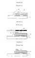
- the CMOS image sensorincludes: a photo-sensing sensor 1 composed of photo-gates or photo-diodes, etc., to sense light and output electrical signals; a photo-shielding layer 2 made of a metallic layer to prevent any incidence of light on an area other than the photo-sensing area of the photo-sensing sensor 1 ; an inter-layer insulating film 3 formed on the photo-shielding layer 2 ; a color filter layer 4 made of dyed photoresist to transmit and deliver light with a specific wavelength to the photo-sensing sensor 1 ; a planarization layer 5 formed on the color filter layer 4 to overcome faults, steps or surface irregularities in the color filter layer 4 ; and micro-lenses 6 of polymer-based resin formed on the planarization layer 5 to gather light.
- a photo-sensing sensor 1composed of photo-gates or photo-diodes, etc., to sense light and output electrical signals
- a photo-shielding layer 2made
- any light parallel to the optical axes of the micro-lensesis refracted by them and focused at a location on the optical axes. Since one image sensor has tens of thousands of micro-lenses, a clear image is obtained only when the characteristics of respective micro-lenses have the same effect. Accordingly, the performance of the micro-lenses play a crucial role in the quality of image sensors.
- a color filter layer 12is formed on a substrate 11 provided with photo-sensing elements (not shown), such as photo-diodes, of an image sensor. Then, a photoresist 13 for forming the planarization layer is formed on the color filter layer 12 .
- the photoresist for forming the planarization layerhas the characteristics of low-sensitivity and high-transmittance in relation to a light source used in an exposure process during photolithography. Specifically, a negative-type photoresist is used.
- a reticle 15is used to expose a predetermined area of the photoresist 13 to light for forming the planarization layer, as shown in FIG. 2B.
- the area exposed to lightcorresponds to the area where micro-lenses are to be formed in subsequent process steps (a cell area) and the area not exposed to light corresponds to the area where pads are to be formed in subsequent process (a peri, or peripheral, area).
- the photoresist in the area not exposed to lightis then developed and removed to complete the planarization layer 14 .
- a photoresist layer 16 for forming micro-lensesis applied on the whole surface of the substrate, including the planarization layer 14 , as shown in FIGS. 2D and 2E.
- a reticle 18is then used to expose the photoresist 16 for forming micro-lenses to light selectively.
- a positive-type photoresistis used as the photoresist for forming micro-lenses. The area not exposed to light corresponds to the area where micro-lenses are to be formed.
- a baking processmay be performed at a temperature of about 150° C. In this process, cuboid-shaped bodies of photoresist 17 melt to form convex micro-lenses that maintain their convex shape upon subsequent cooling.
- the planarization layer to be formed on the color filter layercannot be formed on the peri area but on the cell area only. This causes a topographical fault, or step, between the peri area and the cell area.
- the photoresist for forming micro-lenses on the planarization layergenerally does not have a uniform thickness over the entire surface of the substrate. A fault (believed to be caused by poor step coverage of the photoresist) then occurs at the interface between the peri area and the cell area.
- the final micro-lensesdo not necessarily all have the same shape. In other words, uniform characteristics of all the micro-lenses cannot be guaranteed.
- the area where such irregularly shaped micro-lenses are formedis the interface between the cell area and the peri area, as mentioned above.
- an object of the present inventionis to provide a method of manufacturing a CMOS image sensor making it possible to form micro-lenses having a more uniform shape over an entire substrate.
- a method of manufacturing a CMOS image sensorincluding: coating a color filter layer on or over a semiconductor substrate with a first photoresist; selectively exposing predetermined areas of the first photoresist to define a planarization layer; coating the first photoresist with a second photoresist; selectively exposing the second photoresist to define a plurality of micro-lens bodies; and heating the plurality of micro-lens bodies to form a corresponding plurality of micro-lenses.
- the methodfurther comprises removing predetermined parts of the second photoresist after the second selective exposure process, and more preferably, removing predetermined parts of the first photoresist after removing predetermined parts of the second photoresist.
- the methodmay also further comprise forming the color filter layer on or over the semiconduter substrate before coating with the first photoresist.
- the photoresist for forming the planarization layermay have a thickness of 1.3 ⁇ 3 ⁇ m.
- the photoresist for forming micro-lens bodiesmay have a thickness of 1.1 ⁇ 1.3 ⁇ m.
- the photoresist for forming the planarization layermay be a negative-type photoresist.
- the photoresist for forming micro-lens bodiesmay be a positive-type photoresist.
- the photoresist for forming micro-lens bodiesis patterned (e.g., developed) when the photoresist for forming the planarization layer exists in both a peri area and a cell area.
- the photoresist for forming the planarization layeris then patterned (e.g., developed). This avoids any irregular steps or faulting at the interface between the peri area and the cell area. As a result, micro-lenses of a generally uniform shape are obtained in subsequent process steps.
- FIG. 1illustrates the structure of a CMOS image sensor according to the related art
- FIGS. 2A to 2 Fillustrate process steps of a method of manufacturing a CMOS image sensor according to the related art
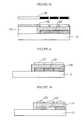
- FIGS. 3A to 3 Fillustrate process steps of a method of manufacturing a CMOS image sensor according to the present invention.
- FIGS. 3A to 3 Fillustrate processes of manufacturing a CMOS image sensor according to the present invention.
- a color filter layer 22is formed on a semiconductor substrate 21 provided with photo-sensing elements (not shown), such as photo-diodes, of an image sensor.
- a photoresist 23 for forming a planarization layeris then formed on the color filter layer 22 .
- the photoresist 23has the characteristics of low-sensitivity and high-transmittance in relation to a light source used in an exposure process during photolithography.
- a negative-type photoresistis used.
- the photoresist 23 for forming the planarization layerpreferably has a thickness of about 1.3-3 ⁇ m.
- a planarization layer reticle 25is used to expose predetermined areas of the photoresist 23 to light, as shown in FIG. 3B.
- the areas exposed to lightcorrespond to the areas where micro-lenses are to be formed in subsequent process steps.
- an area where micro-lenses are to be formedis within a cell area.
- the areas of planarization layer 23 not exposed to lightcorrespond to the areas where pads (and other optional structures) are to be formed in subsequent process steps.
- an area where a pad is to be formedis a peripheral area.
- a second photoresist 26 for forming micro-lensespreferably having a thickness of from about 1.1 to about 1.3 ⁇ m, is then coated on the planarization layer photoresist 23 , as shown in FIG. 3C.
- the photoresist 26 for forming micro-lensesis preferably a positive-type photoresist of high sensitivity.
- a micro-lens reticle 28is subsequently used to expose predetermined areas of the photoresist 26 to light selectively, as shown in FIG. 3D.
- the areas not exposed to lightcorrespond to the areas where micro-lenses are to be formed.
- the energy used in performing the exposure processmust be controlled properly, or the planarization layer photoresist 23 beneath the micro-lens photoresist 26 may be exposed to light.
- the amount of energy used in the exposure processis preferably 300-500mJ.
- the two photoresists 23 and 26may be selected such that the first photoresist has a relatively low sensitivity (e.g., ⁇ 10% or even ⁇ 5%) to the wavelength of light used in the second exposure step, whereas photoresist 26 may have a relatively high sensitivity (e.g., ⁇ 25%, 35%, 40% or 50%) to that wavelength of light.
- a relatively low sensitivitye.g., ⁇ 10% or even ⁇ 5%
- photoresist 26may have a relatively high sensitivity (e.g., ⁇ 25%, 35%, 40% or 50%) to that wavelength of light.
- the area of the micro-lens photoresist 26 exposed to light and the area of the planarization layer photoresist 23 not exposed to lightare successively developed and removed, as shown in FIG. 3E, thus forming the planarization layer.
- On the planarization layerthere exist unit micro-lens bodies 27 corresponding to the locations of the micro-lenses.
- the planarization layerdefines outer limits to an area where micro-lenses are to be formed; i.e., a cell area.
- a baking processis performed at a temperature of about 150° C. to form micro-lenses, as shown in FIG. 3F.
- the plurality of micro-lens bodiesmelt to form micro-lenses 29 of a convex shape.
- the first photoresist 23may be selected such that it does not melt or reflow to an appreciable extent during the micro-lens baking step.
- the method of manufacturing a CMOS image sensor according to the present inventionhas advantages as follows: when successively forming a planarization layer and micro-lenses on a color filter layer, the micro-lens photoresist is patterned when the planarization layer photoresist exists in both the peripheral area and the cell area. After patterning the micro-lens layer, the planarization layer photoresist is then patterned to form an overcoat. This avoids any irregular steps or faults at the interface between the peripheral area and the cell area. As a result, micro-lenses of a uniform shape are obtained. The reliability of the CMOS image sensor is also improved.
Landscapes
- Solid State Image Pick-Up Elements (AREA)
Abstract
Description
- The entire disclosure of Korean Patent Application No. 10-2002-0087351 filed on Dec. 30, 2002 including specification, claims, drawings and summary, is incorporated herein by reference in its entirety.[0001]
- 1. Field of the Invention[0002]
- The present invention relates to a method of manufacturing a CMOS image sensor, and more particularly to a method of manufacturing a CMOS image sensor making it possible to form micro-lenses having a uniform shape throughout a semiconductor substrate.[0003]
- 2. Description of the Related Art[0004]
- As generally known in the art, an “image sensor”is a semiconductor device, such as a CCD (Charge Coupled Device), a CMOS image sensor, etc., which converts optical image signals into electrical signals. The CCD has respective MOS capacitors positioned very close to each other for storing and delivering electrical charge carriers. The CMOS image sensor has adapted a switching mode by making MOS transistors as many as pixels with a CMOS technology, which uses control circuits and signal-processing circuits as peripheral circuits, and by detecting outputs in turn with the MOS transistors. In making such an image sensor, in the mean time, efforts are being made to improve the photosensitivity of the image sensor.[0005]
- In general, the CMOS image sensor is composed of a photo-sensing means for sensing light and a CMOS logic circuit for processing sensed light into electrical signals to make them as data. For better photosensitivity, a Fill Factor, which is a ratio between the area of the photo-sensing means and the whole area of the image sensor, should be increased.[0006]
- In the case of the CMOS image sensor, however, any attempt to increase the area of the photo-sensing means, under the restricted whole area of the sensor, has its limit because of a basic reason that the CMOS logic circuit cannot be eliminated.[0007]
- As an alternative to overcome such problems, a photo-gathering technology has been widely studied that changes the path of light incident on an area other than that over the photo-sensing means and gathers the light into the photo-sensing means for better photosensitivity. An example of the photo-gathering technology is to make convex micro-lenses on top of the photo-sensing means using a material with good photo-transmittance and refract the path of incident light so that more light is transmitted to the photo-sensing means.[0008]
- The structure of a CMOS image sensor using micro-lenses according to the related art will now be explained with reference to FIG. 1. The CMOS image sensor includes: a photo-sensing sensor[0009]1 composed of photo-gates or photo-diodes, etc., to sense light and output electrical signals; a photo-
shielding layer 2 made of a metallic layer to prevent any incidence of light on an area other than the photo-sensing area of the photo-sensing sensor1; aninter-layer insulating film 3 formed on the photo-shielding layer 2; a color filter layer4 made of dyed photoresist to transmit and deliver light with a specific wavelength to the photo-sensing sensor1; aplanarization layer 5 formed on the color filter layer4 to overcome faults, steps or surface irregularities in the color filter layer4; and micro-lenses6 of polymer-based resin formed on theplanarization layer 5 to gather light. - In the case of the CMOS image sensor using micro-lenses as configured above, any light parallel to the optical axes of the micro-lenses is refracted by them and focused at a location on the optical axes. Since one image sensor has tens of thousands of micro-lenses, a clear image is obtained only when the characteristics of respective micro-lenses have the same effect. Accordingly, the performance of the micro-lenses play a crucial role in the quality of image sensors.[0010]
- Processes for manufacturing micro-lenses in the case of the CMOS image sensor of FIG. 1 will now be described with reference to FIGS. 2A to[0011]2F.
- First, as shown in FIG. 2A, a[0012]
color filter layer 12 is formed on asubstrate 11 provided with photo-sensing elements (not shown), such as photo-diodes, of an image sensor. Then, aphotoresist 13 for forming the planarization layer is formed on thecolor filter layer 12. The photoresist for forming the planarization layer has the characteristics of low-sensitivity and high-transmittance in relation to a light source used in an exposure process during photolithography. Specifically, a negative-type photoresist is used. - Next, a[0013]
reticle 15 is used to expose a predetermined area of thephotoresist 13 to light for forming the planarization layer, as shown in FIG. 2B. The area exposed to light corresponds to the area where micro-lenses are to be formed in subsequent process steps (a cell area) and the area not exposed to light corresponds to the area where pads are to be formed in subsequent process (a peri, or peripheral, area). The photoresist in the area not exposed to light is then developed and removed to complete theplanarization layer 14. - [ADD “14” TO FIG[0014]2B.]
- Thereafter, a[0015]
photoresist layer 16 for forming micro-lenses is applied on the whole surface of the substrate, including theplanarization layer 14, as shown in FIGS. 2D and 2E. Areticle 18 is then used to expose thephotoresist 16 for forming micro-lenses to light selectively. A positive-type photoresist is used as the photoresist for forming micro-lenses. The area not exposed to light corresponds to the area where micro-lenses are to be formed. - In this state, the areas of the[0016]
photoresist 16 exposed to light are developed and removed, as shown in FIG. 2F. Next, although not shown in the drawings, a baking process may be performed at a temperature of about 150° C. In this process, cuboid-shaped bodies ofphotoresist 17 melt to form convex micro-lenses that maintain their convex shape upon subsequent cooling. - According to the related method of manufacturing a CMOS image sensor, the planarization layer to be formed on the color filter layer cannot be formed on the peri area but on the cell area only. This causes a topographical fault, or step, between the peri area and the cell area. As a result, the photoresist for forming micro-lenses on the planarization layer generally does not have a uniform thickness over the entire surface of the substrate. A fault (believed to be caused by poor step coverage of the photoresist) then occurs at the interface between the peri area and the cell area.[0017]
- Consequently, the final micro-lenses do not necessarily all have the same shape. In other words, uniform characteristics of all the micro-lenses cannot be guaranteed. The area where such irregularly shaped micro-lenses are formed is the interface between the cell area and the peri area, as mentioned above.[0018]
- Accordingly, the present invention has been made to solve the above-mentioned problems occurring in the related art, and an object of the present invention is to provide a method of manufacturing a CMOS image sensor making it possible to form micro-lenses having a more uniform shape over an entire substrate.[0019]
- In order to accomplish at least the above object, in whole or in parts, there is provided a method of manufacturing a CMOS image sensor including: coating a color filter layer on or over a semiconductor substrate with a first photoresist; selectively exposing predetermined areas of the first photoresist to define a planarization layer; coating the first photoresist with a second photoresist; selectively exposing the second photoresist to define a plurality of micro-lens bodies; and heating the plurality of micro-lens bodies to form a corresponding plurality of micro-lenses.[0020]
- Preferably, the method further comprises removing predetermined parts of the second photoresist after the second selective exposure process, and more preferably, removing predetermined parts of the first photoresist after removing predetermined parts of the second photoresist. The method may also further comprise forming the color filter layer on or over the semiconduter substrate before coating with the first photoresist.[0021]
- Preferably, the photoresist for forming the planarization layer may have a thickness of 1.3˜3 μm.[0022]
- Preferably, the photoresist for forming micro-lens bodies may have a thickness of 1.1˜1.3 μm.[0023]
- Preferably, the photoresist for forming the planarization layer may be a negative-type photoresist.[0024]
- Preferably, the photoresist for forming micro-lens bodies may be a positive-type photoresist.[0025]
- According to the characteristic features of the present invention, when forming the planarization layer and micro-lenses on the color filter layer successively, the photoresist for forming micro-lens bodies is patterned (e.g., developed) when the photoresist for forming the planarization layer exists in both a peri area and a cell area. The photoresist for forming the planarization layer is then patterned (e.g., developed). This avoids any irregular steps or faulting at the interface between the peri area and the cell area. As a result, micro-lenses of a generally uniform shape are obtained in subsequent process steps.[0026]
- The above and other objects, features and advantages of the present invention will be more apparent from the following detailed description taken in conjunction with the accompanying drawings, in which:[0027]
- FIG. 1 illustrates the structure of a CMOS image sensor according to the related art;[0028]
- FIGS. 2A to[0029]2F illustrate process steps of a method of manufacturing a CMOS image sensor according to the related art; and
- FIGS. 3A to[0030]3F illustrate process steps of a method of manufacturing a CMOS image sensor according to the present invention.
- Hereinafter, the preferred embodiments of the present invention will be described with reference to the accompanying drawings, in order to explain the present invention in detail so that those skilled in the art can carry out the present invention easily. FIGS. 3A to[0031]3F illustrate processes of manufacturing a CMOS image sensor according to the present invention.
- For reference, the embodiments disclosed herein include preferred embodiments chosen from among various possible embodiments, and they are provided for aiding the understanding of those skilled in the art. They are not intended to limit nor restrict the technical ideas of the present invention. Accordingly, various modifications, additions and substitutions are possible, without departing from the scope and spirit of the invention and other equivalent embodiments are also possible.[0032]
- First, as shown in FIG. 3A, a[0033]
color filter layer 22 is formed on asemiconductor substrate 21 provided with photo-sensing elements (not shown), such as photo-diodes, of an image sensor. Aphotoresist 23 for forming a planarization layer is then formed on thecolor filter layer 22. Thephotoresist 23 has the characteristics of low-sensitivity and high-transmittance in relation to a light source used in an exposure process during photolithography. Preferably, a negative-type photoresist is used. Thephotoresist 23 for forming the planarization layer preferably has a thickness of about 1.3-3μm. - In this state, a[0034]
planarization layer reticle 25 is used to expose predetermined areas of thephotoresist 23 to light, as shown in FIG. 3B. The areas exposed to light correspond to the areas where micro-lenses are to be formed in subsequent process steps. Typically, an area where micro-lenses are to be formed is within a cell area. The areas ofplanarization layer 23 not exposed to light correspond to the areas where pads (and other optional structures) are to be formed in subsequent process steps. Typically, an area where a pad is to be formed is a peripheral area. - A[0035]
second photoresist 26 for forming micro-lenses, preferably having a thickness of from about 1.1 to about 1.3μm, is then coated on theplanarization layer photoresist 23, as shown in FIG. 3C. Thephotoresist 26 for forming micro-lenses is preferably a positive-type photoresist of high sensitivity. - A[0036]
micro-lens reticle 28 is subsequently used to expose predetermined areas of thephotoresist 26 to light selectively, as shown in FIG. 3D. The areas not exposed to light correspond to the areas where micro-lenses are to be formed. The energy used in performing the exposure process must be controlled properly, or theplanarization layer photoresist 23 beneath themicro-lens photoresist 26 may be exposed to light. The amount of energy used in the exposure process is preferably 300-500mJ. Alternatively and/or additionally, the twophotoresists photoresist 26 may have a relatively high sensitivity (e.g., ≧25%, 35%, 40% or 50%) to that wavelength of light. - Next, the area of the[0037]
micro-lens photoresist 26 exposed to light and the area of theplanarization layer photoresist 23 not exposed to light are successively developed and removed, as shown in FIG. 3E, thus forming the planarization layer. On the planarization layer, there existunit micro-lens bodies 27 corresponding to the locations of the micro-lenses. The planarization layer defines outer limits to an area where micro-lenses are to be formed; i.e., a cell area. - Finally, a baking process is performed at a temperature of about 150° C. to form micro-lenses, as shown in FIG. 3F. During this step, the plurality of micro-lens bodies melt to form micro-lenses[0038]29 of a convex shape. Also, referring back to FIG. 3A, the
first photoresist 23 may be selected such that it does not melt or reflow to an appreciable extent during the micro-lens baking step. - The method of manufacturing a CMOS image sensor according to the present invention has advantages as follows: when successively forming a planarization layer and micro-lenses on a color filter layer, the micro-lens photoresist is patterned when the planarization layer photoresist exists in both the peripheral area and the cell area. After patterning the micro-lens layer, the planarization layer photoresist is then patterned to form an overcoat. This avoids any irregular steps or faults at the interface between the peripheral area and the cell area. As a result, micro-lenses of a uniform shape are obtained. The reliability of the CMOS image sensor is also improved.[0039]
- Although a preferred embodiment of the present invention has been described for illustrative purposes, those skilled in the art will appreciate that various modifications, additions and substitutions are possible, without departing from the scope and spirit of the invention as disclosed in the accompanying claims.[0040]
Claims (14)
Applications Claiming Priority (2)
| Application Number | Priority Date | Filing Date | Title |
|---|---|---|---|
| KR1020020087351AKR100972059B1 (en) | 2002-12-30 | 2002-12-30 | Manufacturing Method of CMOS Image Sensor Improved Coating Uniformity of Micro Lens |
| KR10-2002-0087351 | 2002-12-30 |
Publications (2)
| Publication Number | Publication Date |
|---|---|
| US20040142568A1true US20040142568A1 (en) | 2004-07-22 |
| US7094519B2 US7094519B2 (en) | 2006-08-22 |
Family
ID=32709762
Family Applications (1)
| Application Number | Title | Priority Date | Filing Date |
|---|---|---|---|
| US10/746,703Expired - LifetimeUS7094519B2 (en) | 2002-12-30 | 2003-12-24 | Method of manufacturing a CMOS image sensor |
Country Status (3)
| Country | Link |
|---|---|
| US (1) | US7094519B2 (en) |
| JP (1) | JP3845634B2 (en) |
| KR (1) | KR100972059B1 (en) |
Cited By (4)
| Publication number | Priority date | Publication date | Assignee | Title |
|---|---|---|---|---|
| US7205569B2 (en) | 2005-01-25 | 2007-04-17 | Au Optronics Corp. | Thin film transistor with microlens structures |
| CN100423282C (en)* | 2004-12-24 | 2008-10-01 | 东部亚南半导体株式会社 | CMOS image sensor and manufacturing method thereof |
| US20130201347A1 (en)* | 2012-02-06 | 2013-08-08 | Stmicroelectronics, Inc. | Presence detection device |
| US20190238227A1 (en)* | 2016-08-30 | 2019-08-01 | Telefonaktiebolaget Lm Ericsson (Publ) | Method and Apparatus for Optical Wireless Communication |
Families Citing this family (1)
| Publication number | Priority date | Publication date | Assignee | Title |
|---|---|---|---|---|
| US8389920B2 (en)* | 2008-03-13 | 2013-03-05 | Aptina Imaging Corporation | Method and apparatus for breaking surface tension during a recessed color filter array process |
Citations (17)
| Publication number | Priority date | Publication date | Assignee | Title |
|---|---|---|---|---|
| US5316640A (en)* | 1991-06-19 | 1994-05-31 | Matsushita Electric Industrial Co., Ltd. | Fabricating method of micro lens |
| US5841126A (en)* | 1994-01-28 | 1998-11-24 | California Institute Of Technology | CMOS active pixel sensor type imaging system on a chip |
| US5853960A (en)* | 1998-03-18 | 1998-12-29 | Trw Inc. | Method for producing a micro optical semiconductor lens |
| US5886659A (en)* | 1996-08-21 | 1999-03-23 | California Institute Of Technology | On-focal-plane analog-to-digital conversion for current-mode imaging devices |
| US5976907A (en)* | 1995-05-02 | 1999-11-02 | Matsushita Electronics Corporation | Solid state imaging device and production method for the same |
| US5987137A (en)* | 1996-06-06 | 1999-11-16 | Nokia Mobile Phones, Ltd. | Method for the encryption of data transfer |
| US5990506A (en)* | 1996-03-20 | 1999-11-23 | California Institute Of Technology | Active pixel sensors with substantially planarized color filtering elements |
| US6005619A (en)* | 1997-10-06 | 1999-12-21 | Photobit Corporation | Quantum efficiency improvements in active pixel sensors |
| US6021172A (en)* | 1994-01-28 | 2000-02-01 | California Institute Of Technology | Active pixel sensor having intra-pixel charge transfer with analog-to-digital converter |
| US6023689A (en)* | 1997-02-07 | 2000-02-08 | Nokia Mobile Phones Limited | Method for secure communication in a telecommunications system |
| US6119020A (en)* | 1997-12-16 | 2000-09-12 | Motorola, Inc. | Multiple user SIM card secured subscriber unit |
| US6223290B1 (en)* | 1998-05-07 | 2001-04-24 | Intel Corporation | Method and apparatus for preventing the fraudulent use of a cellular telephone |
| US6324402B1 (en)* | 1997-10-07 | 2001-11-27 | Nortel Dasa Network System Gmbh & Co. Kg | Integration scheme for a mobile telephone |
| US6484260B1 (en)* | 1998-04-24 | 2002-11-19 | Identix, Inc. | Personal identification system |
| US6543686B1 (en)* | 1998-02-16 | 2003-04-08 | Swisscom Ag | Identification card and billing process with an identification card |
| US6580906B2 (en)* | 1997-12-10 | 2003-06-17 | Intel Corporation | Authentication and security in wireless communication system |
| US6861207B2 (en)* | 2003-06-30 | 2005-03-01 | Taiwan Semiconductor Manufacturing Company, Ltd. | Method for fabricating microlens with lithographic process |
Family Cites Families (7)
| Publication number | Priority date | Publication date | Assignee | Title |
|---|---|---|---|---|
| JPH06349728A (en) | 1993-06-14 | 1994-12-22 | Sony Corp | Formation of resist pattern |
| JPH081809A (en)* | 1994-06-22 | 1996-01-09 | Casio Comput Co Ltd | Microlens formation method |
| JP2802733B2 (en) | 1995-06-07 | 1998-09-24 | エルジイ・セミコン・カンパニイ・リミテッド | Color solid-state imaging device and method of manufacturing the same |
| JPH10294826A (en) | 1997-04-18 | 1998-11-04 | Sharp Corp | Color image sensor |
| KR20000041461A (en)* | 1998-12-22 | 2000-07-15 | 김영환 | Fabrication method of improved image sensor |
| KR100477784B1 (en)* | 2000-08-31 | 2005-03-22 | 매그나칩 반도체 유한회사 | Image sensor having lens formed by air in trench and method for fabricating the same |
| JP2002178156A (en) | 2000-12-18 | 2002-06-25 | Aiseihaado Kk | Welding member using plasma powder welding and welding method for the same |
- 2002
- 2002-12-30KRKR1020020087351Apatent/KR100972059B1/ennot_activeExpired - Fee Related
- 2003
- 2003-12-24USUS10/746,703patent/US7094519B2/ennot_activeExpired - Lifetime
- 2003-12-26JPJP2003432896Apatent/JP3845634B2/ennot_activeExpired - Fee Related
Patent Citations (17)
| Publication number | Priority date | Publication date | Assignee | Title |
|---|---|---|---|---|
| US5316640A (en)* | 1991-06-19 | 1994-05-31 | Matsushita Electric Industrial Co., Ltd. | Fabricating method of micro lens |
| US5841126A (en)* | 1994-01-28 | 1998-11-24 | California Institute Of Technology | CMOS active pixel sensor type imaging system on a chip |
| US6021172A (en)* | 1994-01-28 | 2000-02-01 | California Institute Of Technology | Active pixel sensor having intra-pixel charge transfer with analog-to-digital converter |
| US5976907A (en)* | 1995-05-02 | 1999-11-02 | Matsushita Electronics Corporation | Solid state imaging device and production method for the same |
| US5990506A (en)* | 1996-03-20 | 1999-11-23 | California Institute Of Technology | Active pixel sensors with substantially planarized color filtering elements |
| US5987137A (en)* | 1996-06-06 | 1999-11-16 | Nokia Mobile Phones, Ltd. | Method for the encryption of data transfer |
| US5886659A (en)* | 1996-08-21 | 1999-03-23 | California Institute Of Technology | On-focal-plane analog-to-digital conversion for current-mode imaging devices |
| US6023689A (en)* | 1997-02-07 | 2000-02-08 | Nokia Mobile Phones Limited | Method for secure communication in a telecommunications system |
| US6005619A (en)* | 1997-10-06 | 1999-12-21 | Photobit Corporation | Quantum efficiency improvements in active pixel sensors |
| US6324402B1 (en)* | 1997-10-07 | 2001-11-27 | Nortel Dasa Network System Gmbh & Co. Kg | Integration scheme for a mobile telephone |
| US6580906B2 (en)* | 1997-12-10 | 2003-06-17 | Intel Corporation | Authentication and security in wireless communication system |
| US6119020A (en)* | 1997-12-16 | 2000-09-12 | Motorola, Inc. | Multiple user SIM card secured subscriber unit |
| US6543686B1 (en)* | 1998-02-16 | 2003-04-08 | Swisscom Ag | Identification card and billing process with an identification card |
| US5853960A (en)* | 1998-03-18 | 1998-12-29 | Trw Inc. | Method for producing a micro optical semiconductor lens |
| US6484260B1 (en)* | 1998-04-24 | 2002-11-19 | Identix, Inc. | Personal identification system |
| US6223290B1 (en)* | 1998-05-07 | 2001-04-24 | Intel Corporation | Method and apparatus for preventing the fraudulent use of a cellular telephone |
| US6861207B2 (en)* | 2003-06-30 | 2005-03-01 | Taiwan Semiconductor Manufacturing Company, Ltd. | Method for fabricating microlens with lithographic process |
Cited By (4)
| Publication number | Priority date | Publication date | Assignee | Title |
|---|---|---|---|---|
| CN100423282C (en)* | 2004-12-24 | 2008-10-01 | 东部亚南半导体株式会社 | CMOS image sensor and manufacturing method thereof |
| US7205569B2 (en) | 2005-01-25 | 2007-04-17 | Au Optronics Corp. | Thin film transistor with microlens structures |
| US20130201347A1 (en)* | 2012-02-06 | 2013-08-08 | Stmicroelectronics, Inc. | Presence detection device |
| US20190238227A1 (en)* | 2016-08-30 | 2019-08-01 | Telefonaktiebolaget Lm Ericsson (Publ) | Method and Apparatus for Optical Wireless Communication |
Also Published As
| Publication number | Publication date |
|---|---|
| KR100972059B1 (en) | 2010-07-22 |
| US7094519B2 (en) | 2006-08-22 |
| KR20040060544A (en) | 2004-07-06 |
| JP3845634B2 (en) | 2006-11-15 |
| JP2004214672A (en) | 2004-07-29 |
Similar Documents
| Publication | Publication Date | Title |
|---|---|---|
| KR100869219B1 (en) | Image sensor and its manufacturing method | |
| US7898049B2 (en) | Touching microlens structure for a pixel sensor and method of fabrication | |
| TWI424556B (en) | Solid-state imaging device, manufacturing method thereof, and camera | |
| JP2004235635A (en) | Method for manufacturing CMOS image sensor | |
| US8030117B2 (en) | Image sensor and method for manufacturing the same | |
| US7723147B2 (en) | Image sensor and method of manufacturing the same | |
| JP3711211B2 (en) | Solid-state imaging device | |
| US7060592B2 (en) | Image sensor and fabricating method thereof | |
| TWI222178B (en) | Manufacturing method of image sensor device | |
| US7094519B2 (en) | Method of manufacturing a CMOS image sensor | |
| KR100649031B1 (en) | Manufacturing Method of CMOS Image Sensor | |
| US20070102716A1 (en) | Image sensor and fabricating method thereof | |
| JPH10107238A (en) | Solid state image-sensing device and its manufacture | |
| KR100915758B1 (en) | Method for Manufacturing An Image Sensor | |
| JP2005353631A (en) | Manufacturing method of solid-state image pickup device | |
| US6699729B1 (en) | Method of forming planar color filters in an image sensor | |
| CN100490163C (en) | Method for manufacturing image sensor element | |
| KR20050032867A (en) | Complementary metal oxide semiconductor image sensor and method for fabricating thereof | |
| KR100757653B1 (en) | Manufacturing Method of Photosensitive Device | |
| KR100595601B1 (en) | CMOS image sensor manufacturing method | |
| US20080272452A1 (en) | Image sensor and method for manufacturing the same | |
| US20070145238A1 (en) | Method for Manufacturing Mask and CMOS Image Sensor | |
| KR100952766B1 (en) | Manufacturing method of CMOS image sensor with redundancy module | |
| JP2951942B1 (en) | Method for manufacturing solid-state imaging device | |
| KR20050051267A (en) | Method for manufacturing a image sensor |
Legal Events
| Date | Code | Title | Description |
|---|---|---|---|
| AS | Assignment | Owner name:DONGBU ELECTRONICS CO., LTD., KOREA, REPUBLIC OF Free format text:ASSIGNMENT OF ASSIGNORS INTEREST;ASSIGNOR:JUNG, MENG AN;REEL/FRAME:014859/0459 Effective date:20031223 | |
| FEPP | Fee payment procedure | Free format text:PAYOR NUMBER ASSIGNED (ORIGINAL EVENT CODE: ASPN); ENTITY STATUS OF PATENT OWNER: LARGE ENTITY Free format text:PAYER NUMBER DE-ASSIGNED (ORIGINAL EVENT CODE: RMPN); ENTITY STATUS OF PATENT OWNER: LARGE ENTITY | |
| AS | Assignment | Owner name:DONGBUANAM SEMICONDUCTOR INC., KOREA, REPUBLIC OF Free format text:MERGER;ASSIGNOR:DONGBU ELECTRONICS CO., LTD.;REEL/FRAME:017251/0452 Effective date:20041221 | |
| AS | Assignment | Owner name:DONGBU ELECTRONICS CO., LTD., KOREA, REPUBLIC OF Free format text:CHANGE OF NAME;ASSIGNOR:DONGBUANAM SEMICONDUCTOR INC.;REEL/FRAME:017616/0966 Effective date:20060328 | |
| STCF | Information on status: patent grant | Free format text:PATENTED CASE | |
| FEPP | Fee payment procedure | Free format text:PAYER NUMBER DE-ASSIGNED (ORIGINAL EVENT CODE: RMPN); ENTITY STATUS OF PATENT OWNER: LARGE ENTITY | |
| FPAY | Fee payment | Year of fee payment:4 | |
| FPAY | Fee payment | Year of fee payment:8 | |
| AS | Assignment | Owner name:DONGBU HITEK CO., LTD., KOREA, REPUBLIC OF Free format text:MERGER AND CHANGE OF NAME;ASSIGNORS:DONGBU ELECTRONICS CO., LTD.;DONGBU HITEK CO., LTD.;REEL/FRAME:044533/0523 Effective date:20070503 | |
| AS | Assignment | Owner name:DB HITEK CO., LTD, KOREA, REPUBLIC OF Free format text:CHANGE OF NAME;ASSIGNOR:DONGBU HITEK CO., LTD.;REEL/FRAME:044555/0913 Effective date:20171101 | |
| MAFP | Maintenance fee payment | Free format text:PAYMENT OF MAINTENANCE FEE, 12TH YEAR, LARGE ENTITY (ORIGINAL EVENT CODE: M1553) Year of fee payment:12 | |
| AS | Assignment | Owner name:COLUMBA TECHNOLOGIES INC., CANADA Free format text:ASSIGNMENT OF ASSIGNORS INTEREST;ASSIGNOR:DB HITEK CO., LTD.;REEL/FRAME:049709/0857 Effective date:20190125 | |
| AS | Assignment | Owner name:TAIWAN SEMICONDUCTOR MANUFACTURING CO., LTD., TAIWAN Free format text:ASSIGNMENT OF ASSIGNORS INTEREST;ASSIGNOR:COLUMBA TECHNOLOGIES, INC.;REEL/FRAME:052845/0474 Effective date:20200211 |