US20040135520A1 - Organic electroluminescent device and manufacturing method for the same - Google Patents
Organic electroluminescent device and manufacturing method for the sameDownload PDFInfo
- Publication number
- US20040135520A1 US20040135520A1US10/742,775US74277503AUS2004135520A1US 20040135520 A1US20040135520 A1US 20040135520A1US 74277503 AUS74277503 AUS 74277503AUS 2004135520 A1US2004135520 A1US 2004135520A1
- Authority
- US
- United States
- Prior art keywords
- electrode
- power supply
- gate
- pad
- line
- Prior art date
- Legal status (The legal status is an assumption and is not a legal conclusion. Google has not performed a legal analysis and makes no representation as to the accuracy of the status listed.)
- Granted
Links
Images


Classifications
- H—ELECTRICITY
- H10—SEMICONDUCTOR DEVICES; ELECTRIC SOLID-STATE DEVICES NOT OTHERWISE PROVIDED FOR
- H10K—ORGANIC ELECTRIC SOLID-STATE DEVICES
- H10K59/00—Integrated devices, or assemblies of multiple devices, comprising at least one organic light-emitting element covered by group H10K50/00
- H10K59/10—OLED displays
- H10K59/12—Active-matrix OLED [AMOLED] displays
- H10K59/121—Active-matrix OLED [AMOLED] displays characterised by the geometry or disposition of pixel elements
- H10K59/1213—Active-matrix OLED [AMOLED] displays characterised by the geometry or disposition of pixel elements the pixel elements being TFTs
- H—ELECTRICITY
- H05—ELECTRIC TECHNIQUES NOT OTHERWISE PROVIDED FOR
- H05B—ELECTRIC HEATING; ELECTRIC LIGHT SOURCES NOT OTHERWISE PROVIDED FOR; CIRCUIT ARRANGEMENTS FOR ELECTRIC LIGHT SOURCES, IN GENERAL
- H05B33/00—Electroluminescent light sources
- H05B33/10—Apparatus or processes specially adapted to the manufacture of electroluminescent light sources
- H—ELECTRICITY
- H10—SEMICONDUCTOR DEVICES; ELECTRIC SOLID-STATE DEVICES NOT OTHERWISE PROVIDED FOR
- H10K—ORGANIC ELECTRIC SOLID-STATE DEVICES
- H10K59/00—Integrated devices, or assemblies of multiple devices, comprising at least one organic light-emitting element covered by group H10K50/00
- H10K59/10—OLED displays
- H10K59/12—Active-matrix OLED [AMOLED] displays
- H10K59/127—Active-matrix OLED [AMOLED] displays comprising two substrates, e.g. display comprising OLED array and TFT driving circuitry on different substrates
- H10K59/1275—Electrical connections of the two substrates
Definitions
- the present inventionrelates to a flat panel display device and more particularly, to an organic electroluminescent device and manufacturing method for the same.
- Liquid crystal display (LCD) deviceshave been most widely used in the field of flat panel display devices due to their lightweight and low power consumption.
- the liquid crystal display (LCD) deviceis not a light emitting element but rather a light-receiving element that needs an additional light source to display images. Accordingly, there is a technical limit in improving brightness, contrast ratio, viewing angle and enlarging the size of a liquid crystal display panel. For this reason, mush research has been ongoing in this field to develop a new flat panel display element that can overcome the aforementioned problems.
- the organic electroluminescent deviceis one of the those new flat panel display elements. Because the organic electroluminescent device emits light, allows for a wide viewing angle and a large contrast ratio, the organic electroluminescent device is superior when compared to the liquid crystal display (LCD) device. In addition, an organic electroluminescent device does not need a backlight. Further, an organic electroluminescent device also has the advantages of being light weight, a thin profile and low power consumption. Moreover, the organic electroluminescent device can be driven with a low DC (direct current) and has a fast response time. Because the organic electroluminescent device uses a solid material instead of a fluid material, such as liquid crystal, an organic electroluminescent device is more stable if it receives an external impact. The solid material also has a wider range of operating temperatures as compared to liquid crystal.
- the organic electroluminescent devicealso has an advantage in terms of production costs as compared to an LCD device. Specifically, a deposition apparatus and an encapsulation apparatus are all that is needed for manufacturing an organic electroluminescent device, while the liquid crystal display (LCD) device or Plasma display panels (PDPs) need many kind of apparatus. Thus, the manufacturing process for the organic electroluminescent device is very simple compared to the liquid crystal display (LCD) device or the plasma display panels (PDPs).
- Organic electroluminescent devicesmay be classified into either a passive matrix-type device or an active matrix-type device.
- the active matrix-type organic electroluminescent devicevoltage applied to the pixel is also stored in a storage capacitor C ST such that the voltage is maintained until a signal for the next frame is applied. Accordingly, the pixel can retain the signal until the next frame regardless of the number of the scan lines.
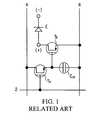
- the active matrix-type organic electroluminescent devicecan obtain an appropriate luminance with low direct current (DC). Further, the active matrix-type organic electroluminescent device has advantages, such as low power consumption and high resolution with a large screen size. A basic structure and an operational property of the active matrix-type organic electroluminescent device will be described hereinafter with reference to FIG. 1.
- FIG. 1is a circuit diagram of a pixel of a related art active matrix organic electroluminescent device. A basic structure and an operational property of the active matrix-type organic electroluminescent device will be described hereinafter with reference to FIG. 1.
- a scan line 2is formed in a first direction while signal and power supply lines 4 and 6 , formed apart from each other and crossing the scan line 2 , are formed in a second direction.
- the scan line 2 together with the signal and power supply lines 4 and 6define a pixel region.
- a switching thin film transistor T Ssuch as an addressing element, is formed near an intersection of the scan and signal lines 2 and 4 , and a storage capacitor C ST is connected to the switching thin film transistor T S .
- a driving thin film transistor T Dsuch as a current source element, is connected to the switching thin film transistor T S , the storage capacitor C ST and the power supply line 6 .
- the driving thin film transistor T Dis electrically connected to an anode electrode of an organic electroluminescent diode E that is driven by a static current.
- the anode electrode as well as the cathode electrodeare components of the organic electroluminescent diode E.
- the switching thin film transistor T Sserves to control a voltage applied to the driving thin film transistor T S and the storage capacitor C ST serves to store a charge to maintain the voltage applied to the driving thin film transistor T S .
- the driving principle of the related art organic electroluminescent devicewill be described hereinafter.
- a data signalcan be applied to the driving thin film transistor T D and the storage capacitor C ST via the switching thin film transistor T S .
- a current from the power supply line 6can be applied to the organic electroluminescent diode E.
- the current passing through the driving thin film transistor T Dthen passes through the organic electroluminescent diode E such that the organic electroluminescent diode E can emit light.
- gray levelscan be displayed by controlling an amount of current that passes through the driving thin film transistor T D .
- a data signal that is stored in the storage capacitor C STis continuously applied to the driving thin film transistor T D and accordingly the organic electroluminescent diode E can continuously emit light at a specified gray level until a signal for a next frame is applied.
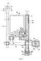
- FIG. 2is a plan view of a pixel of a related art active matrix organic electroluminescent device.
- the pixelincludes a switching thin film transistor T S and a driving thin film transistor T D .
- a gate line 37is formed in a first direction, and a data line 51 and a power supply line 41 , which are spaced apart from each other, are formed in a second direction.
- the gate line 37crosses the data line 51 and the power supply line 41 and defines a pixel region P between the gate line 37 , the data line 51 and the power supply line 41 .
- a switching thin film transistor T Sis formed near an intersection of the gate and the data lines 37 and 51 and a driving thin film transistor T D is formed near an intersection of the switching thin film transistor T S and the power supply line- 41 .
- the power supply line 41 and a capacitor electrode 34which is connected to a semiconductor layer 31 of the switching thin film transistor T S , form a storage capacitor C ST .
- a first electrode 58is electrically connected to the driving thin film transistor T D .
- an organic light emitting layer and a second electrodeare sequentially formed over the first electrode 58 .
- the area where the first electrode 58 is formedis defined as an organic light-emitting region L.
- the driving thin film transistor T Dhas a semiconductor layer 32 and a gate electrode 38 .
- the switching thin film transistor T Shas a gate electrode 35 . Layered structures of the organic light-emitting region L, the driving thin film transistor T D and the storage capacitor C ST will be described hereinafter with reference to FIG. 3.
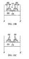
- FIG. 3is a cross-sectional view along the line III-III′ of FIG. 2.
- a driving thin film transistor T Dhaving a semiconductor layer 32 , a gate electrode 38 , and source and drain electrodes 50 and 52 is formed on an insulating substrate 1 .
- a power electrode 42 extending from a power supply line (not shown)is electrically connected to the source electrode 50 and a first electrode formed of transparent conductive material is electrically connected to the drain electrode 52 .
- a capacitor electrode 34is formed under the power electrode 42 of the same material used to form the semiconductor layer 32 .
- the power electrode 42 and the capacitor electrode 34form a storage capacitor C ST .
- An organic light-emitting layer 64 and a cathode electrode 66are sequentially formed on the first electrode 58 to complete formation of an organic light-emitting region L.
- a buffer layer 30is formed between the substrate 1 and the semiconductor layer 32 .
- First, second, third and fourth passivation layers 40 , 44 , 54 and 60 respectively having a contact hole for electrical contacting in each layerare formed on the substrate 1 .
- the first passivation layer 40is formed between the storage electrode 34 and the power electrode 42 and serves as a dielectric substance.
- the second passivation layer 44is formed on the power electrode 42 and the third passivation layer 54 is formed between the source electrode 50 and the first electrode 58 .
- the fourth passivation layer 60is formed between the driving thin film transistor T D and a second electrode 66 .
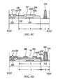
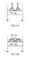
- FIGS. 4A to 4 Iare cross-sectional views illustrating processes of fabricating the related art active matrix organic electroluminescent device, and correspond to cross-sections along the line III-III′ of FIG. 2.
- the organic electroluminescent devicemay be manufactured using a photolithographic process in which thin films are patterned by exposing and then developing a photoresist, such as a photosensitive material.
- a buffer layer 30is formed on an insulating substrate 1 with a first insulating material.
- a semiconductor layer 32 and a capacitor electrode 34are formed of polycrystalline silicon on the buffer layer 30 through a first photolithography process using a first mask.
- a gate insulating layer 36 and a gate electrode 38are formed on the semiconductor layer 32 by sequentially depositing a second insulating material and a first metal material on the semiconductor layer 32 and then patterning the deposited material through a second photolithography process using a second mask.
- a first passivation layer 40is formed on the whole substrate on which the gate insulating layer 36 and the gate electrode 38 are already formed.
- a power electrode 42is subsequently formed on the first passivation layer 40 in an area corresponding to the capacitor electrode 34 by depositing a second metal material on the first passivation layer 40 and then patterning it through a third photolithography process using a third mask.
- a second passivation layer 44 having first and second contact holes 46 a and 46 b and a capacitor contact hole 48is formed in the first passivation layer 40 by depositing a third insulating material on the first passivation layer 40 and then patterning it through a fourth photolithography process using a fourth mask.
- the first and second contact holes 46 a and 46 bexpose portions at both sides of the semiconductor layer 32 and the capacitor contact hole 48 exposes a portion of the power electrode 42 .
- the semiconductor layer 32is doped with impurities such as boron (B) or phosphorus (P) to define a channel region 32 a corresponding to the gate electrode 38 , and source and drain regions 32 b and 32 c at both sides of the channel region 32 a.
- impuritiessuch as boron (B) or phosphorus (P)
- source and drain electrodes 50 and 52are subsequently formed on the second passivation layer 44 by depositing a third metal material and then patterning it through a fifth photolithography process using a fifth mask.
- the source electrode 50is connected to the source region 32 b through the first contact hole 46 a and is connected to the power electrode 42 via the capacitor contact hole 48 .
- the drain electrode 52is connected to the drain region 32 c via the second contact hole 46 b .
- the semiconductor layer 32 , the gate electrode 38 and the source and drain electrodes 50 and 52form a driving thin film transistor T D .
- the power electrode 42 and the capacitor electrode 34are electrically connected to the source electrode 52 and a semiconductor layer (not shown) of a switching thin film transistor (not shown), respectively and form a storage capacitor C ST using the first passivation layer 40 as a dielectric substance.
- a third passivation layer 54 having a drain contact hole 56is formed by depositing a fourth insulating material over the whole substrate 1 on which the source and drain electrodes 50 and 52 are already formed and then patterning it through a sixth photolithography process using a sixth mask.
- a first electrode 58is then formed on the third passivation layer 54 in an area corresponding to an organic light-emitting region L by depositing a fourth metal material on the third passivation layer 54 and then patterning it through a seventh photolithography process using a seventh mask.
- the first electrode 58is connected to the drain electrode 52 through the drain contact hole 56 .
- a fourth passivation layer 60 having a first electrode exposure portion 62exposes a first electrode portion corresponding to the organic light-emitting region L formed by depositing a fifth insulating material over the whole substrate 1 on which the first electrode 58 is already formed and then patterning it through an eighth photolithography process using an eighth mask.
- the fourth passivation layer 60also serves to protect the driving thin film transistor T D from moisture and contaminants.
- an organic light-emitting layer 64 contacting the first electrode 58 via the first electrode exposure portion 62is formed on the substrate 1 over which the fourth passivation layer 60 is already formed.
- a second electrode 66is subsequently formed on the organic light-emitting layer 64 and the fourth passivation layer 60 by depositing a fifth metal material over the whole substrate 1 . If the first electrode 58 is used as an anode electrode, the fifth metal material should have a reflection property so as to reflect the light emitted from the organic light-emitting layer 64 and thus to display an image.
- the fifth metal materialis selected from the metal materials having a low work function such that the second electrode 66 can easily give away electrons.
- FIG. 5is a cross-sectional view of a related art organic electroluminescent device.
- An array element layer 80 having a plurality of driving thin film transistors T D corresponding to each sub-pixel P subis formed on the first substrate 70 .
- a plurality of first electrodes 72 corresponding to each sub-pixel P subis formed on the array element layer 80 .
- the plurality of first electrodes 72respectively connects to the driving thin film transistors T D of the sub-pixels P sub
- An organic light-emitting layer 74 for emitting light of either red (R), green (G) and blue (B) colors from the sub-pixels P subis formed on the first electrode 72 .
- a second electrode 76is formed on the organic light-emitting layer 74 .
- the first and second electrodes 72 and 76 , and the organic light-emitting layer 74form an organic electroluminescent diode E. Light emitted from the organic light-emitting layer 74 passes through the first electrode 72 . That is, the organic electroluminescent device is a bottom emission-type organic electroluminescent device.
- the second substrate 90is used as an encapsulating substrate and has a depressed portion 92 at a middle surface thereof and a moisture absorbent desiccant 94 for protecting the organic electroluminescent diode E from exterior moisture.
- the second substrate 90is spaced apart from the second electrode 76 at a certain distance.
- a seal pattern 85is formed on one of the first and second substrates 70 and 90 and later used to attach the first and second substrates 70 and 90 .
- Bottom emission-type organic electroluminescent deviceshave the advantages of high image stability and variable fabrication processing. However, the bottom emission-type organic electroluminescent devices are not adequate for implementation in devices that require high resolution because bottom emission-type organic electroluminescent devices have a small aperture ratio due to the thin film transistor blocking some of the light transmission. Top emission-type organic electroluminescent devices have a large aperature ratio. In addition, since top emission-type organic electroluminescent devices emit light upward of the substrate, the light can be emitted without being blocked by the thin film transistor that is positioned under the light-emitting layer. Accordingly, design of the thin film transistor may be simplified in top emission-type organic electroluminescent device.
- the aperture ratiocan be increased, thereby increasing operational life span of the organic electroluminescent device.
- a cathodeis commonly formed over the organic light-emitting layer in the top emission-type organic electroluminescent devices, material selection and light transmittance are limited such that light transmission efficiency is lowered. If a thin film-type passivation layer is formed to prevent a reduction of the light transmittance, the thin film passivation layer may fail to prevent infiltration of exterior air into the device.
- the present inventionis directed to an organic electroluminescent device and manufacturing method for the same that substantially obviate one or more of the problems due to limitations and disadvantages of the related art.
- An object of the present inventionis to provide an organic electroluminescent device that is manufactured at lower temperatures with reduced number of masking steps.
- Another object of the present inventionis to provide a manufacturing method for an organic electroluminescent device having lower temperatures and a reduced number of masking steps
- an organic electroluminescent deviceincludes first and second substrates spaced apart from and facing each other, an organic electroluminescent diode on an inner surface of the second substrate, a gate line formed on an inner surface of the first substrate in a first direction, a data line formed in a second direction crossing the first direction, a power supply line spaced apart from the data line and formed in the second direction, the power supply line made of the same material as the gate line, the power supply line having a power supply link line near a crossing portion of the gate line and the power supply line, a switching thin film transistor at a crossing portion of the gate and data lines, the switching thin film transistor including a first semiconductor layer made of amorphous silicon, a driving thin film transistor at a crossing portion of the switching thin film transistor and the power supply line, the driving thin film transistor including a second semiconductor layer made of amorphous silicon, a connecting electrode connected to the driving thin film transistor and made
- a method of manufacturing an array substrate for an organic electroluminescent device including an array element on a first substrate and an organic electroluminescent diode on a second substrateincludes steps of forming a gate electrode, a gate pad, a power electrode and a power supply pad by depositing a first metal material on a substrate and then patterning the first metal material using a first mask process, forming a gate insulating layer, a semiconductor layer, a semiconductor material pattern, a first pattern and a second pattern by depositing a first insulating material, amorphous silicon and doped amorphous silicon on the substrate including the gate electrode, the gate pad, the power electrode and the power supply pad and patterning the first insulating material, the amorphous silicon and the doped amorphous silicon using a second mask process, wherein the semiconductor layer is disposed over the gate electrode and includes the amorphous silicon and the doped amorphous silicon, the semiconductor material pattern extends from the semiconductor layer and has a power
- FIG. 1is a circuit diagram of a pixel of a related art active matrix organic electroluminescent device.
- FIG. 2is a plan view of a pixel of a related art active matrix organic electroluminescent device.
- FIG. 3is a cross-sectional view along the line III-III′ of FIG. 2.
- FIGS. 4A to 4 Iare cross-sectional views illustrating processes of fabricating the related art active matrix organic electroluminescent device and corresponding to cross-sections along the line III-III′ of FIG. 2.
- FIG. 5is a cross-sectional view of a related art organic electroluminescent device.
- FIG. 6is a cross-sectional view of a dual panel type organic electro-luminescent device according to an embodiment of the present invention.
- FIG. 7is a plan view of an array substrate for a dual panel type organic electroluminescent device according to an embodiment of the present invention.
- FIGS. 8A to 8 Eare cross-sectional views along the line VIII-VIII′ of FIG. 7 and illustrating processes of fabricating an array substrate for the dual panel type organic electroluminescent device according to the embodiment of the present invention.
- FIGS. 9A to 9 Gare cross-sectional views along the line IX-IX′ of FIG. 7 and illustrating processes of fabricating an array substrate for the dual panel type organic electroluminescent device according to the embodiment of the present invention.
- FIGS. 10A to 10 Gare cross-sectional views along the line X-X′ of FIG. 7 and illustrating processes of fabricating an array-substrate for the dual panel type organic electroluminescent device according to the embodiment of the present invention.
- FIGS. 11A to 11 Gare cross-sectional views along the line XI-XI′ of FIG. 7 and illustrating processes of fabricating an array substrate for the dual panel type organic electroluminescent device according to the embodiment of the present invention.
- a dual panel type organic electroluminescent device according to the present inventionthat will be described hereinafter is an active matrix top emission type device.
- FIG. 6is a cross-sectional view of a dual panel type organic electroluminescent device according to an embodiment of the present invention.
- a first substrate 110 and a second substrate 150are spaced apart and facing each other.
- a plurality of sub-pixels P subare defined on the first and second substrates 110 and 150 .
- An array element layer 140 having a plurality of driving thin film transistors T D corresponding to each sub-pixel P subis formed on the first substrate 110 .
- An electrical connecting pattern 142 connected to the driving thin film transistor T Dis formed on the array element layer 140 .
- the electrical connecting pattern 142is formed of conductive material and may be formed in a multi-layered structure including an insulating material considering its thickness.
- the electrical connecting pattern 142may be electrically connected to the driving thin film transistor T D via an additional connecting electrode (not shown).
- the driving thin film transistor T Dhas a gate electrode 112 , a semiconductor layer 114 and source and drain electrodes 116 and 118 , and the electrical connecting pattern 142 is directly connected to the drain electrode 118 .
- a first electrode 152is formed on an inner surface of the second substrate 150 .
- An organic light-emitting layer 160having sub-light emitting layers 156 a , 156 b and 156 c respectively for red (R), green (G) and blue (B) colors is formed beneath the first electrode 152 .
- a plurality of second electrodes 162 corresponding to each sub-pixel P subis formed beneath the organic light-emitting layer 160 .
- the organic light-emitting layer 160has a first carrier-delivering layer 154 between the first electrode 152 and the sub-light emitting layers 156 a , 156 b and 156 c and a second carrier-delivering layer 158 between the sub-light emitting layers 156 a , 156 b and 156 c and the second electrode 162 .
- the first electrode 152is an anode electrode and the second electrode 162 is a cathode electrode
- the first carrier-delivering layer 154serves as a hole injection layer and then a hole transporting layer
- the second carrier delivering layer 158serves as an electron transporting layer and then an electron injection layer.
- the first and second electrodes 152 and 162 and the organic light-emitting layer 160 between the first and second electrodes 152 and 162form an organic electroluminescent diode E. Because the electrical connecting pattern 142 contacts the bottom surface of the second electrode 162 , current supplied from the driving thin film transistor T D can be applied to the second electrode 162 via the electrical connecting pattern 142 .
- a seal pattern 170is formed on one of the first and second substrates 110 and 150 such that the first and second substrates 110 and 150 can be attached to one another.
- the array element layer 140 and the organic electroluminescent diode Eare formed on different substrates and are electrically connected to each other by the electrical connecting pattern 142 . That is, the organic electroluminescent device of the present invention is a dual panel type organic electroluminescent device. Only two pixels respectively having three sub-pixels are illustrated in FIG. 6 for convenience of an explanation. Further, the structure of the driving thin film transistor T D and a connecting method of the electrical connecting pattern 142 can be modified for many different conditions. In addition, because the organic electroluminescent device of the present invention is a top emission-type organic electroluminescent device, a driving thin film transistor T D design can be easily obtained while maintaining a high aperture ratio.
- FIG. 7is a plan view of an array substrate for a dual panel type organic electroluminescent device according to an embodiment of the present invention.
- a gate line 214is formed in a first direction and a data line 314 and a power supply line 230 , which are spaced apart from each other, are formed in a second direction perpendicular to the first direction.
- a switching thin film transistor T Sis formed adjacent to where gate line 214 and data line 314 cross each other.
- the switching thin film transistor T Shas a first gate electrode 218 , a first source electrode 282 , a first drain electrode 290 and a first semiconductor layer 254 .
- the first gate electrode 218extends from the gate line 214 and the first source electrode 282 extends from the data line 314 .
- the first drain electrode 290is spaced apart from the first source electrode 282 and the first semiconductor layer 254 overlaps portions of the first gate electrode 218 , the first source electrode 282 and the first drain electrode 290 .
- a first gate insulating layer 250is formed in a shape of a pattern corresponding to the first semiconductor layer 254 .
- the power supply line 230is formed simultaneously with the gate line 214 using the same material that is used to form the gate line 214 .
- a driving thin film transistor T Dis electrically connected to the switching thin film transistor T S and the power supply line 230 .
- the driving thin film transistor T Dhas a second gate electrode 222 , a second source electrode 286 , a second drain electrode 294 and a second semiconductor layer 258 .
- the second gate electrode 222is formed simultaneously with the gate line 214 using the same material that is used to form the gate line 214 .
- the second source and drain electrodes 286 and 294 spaced apart from each otherare formed simultaneously with the data line 314 using the same material that is used to form the data line 314 .
- the second semiconductor layer 258overlaps portions of the second gate electrode 222 , the second source electrode 286 and the second drain electrode 294 .
- a second gate insulating layer 251which is made of the same material that is used to form the first gate insulating layer 250 , is formed in a pattern shape corresponding to the second semiconductor layer 258 .
- a power electrode 232extends from the power supply line 230 and is electrically connected to the second source electrode 286 via a power electrode contact hole 271 .
- a connecting electrode 306which extends from the second drain electrode 294 , is formed in an electrical connecting region A.
- the electrical connecting region Acorresponds to a second electrode of a substrate (not shown) having an organic electroluminescent diode (not shown).
- an electrical connecting pattern having a columnar shapeis formed in the electrical connecting region A. More detail with regard to the electrical connecting pattern (not shown) will be described later.
- a capacitor electrode 298which overlaps the power supply line 230 and is connected to the first drain electrode 290 , is formed under the power supply line 230 .
- the capacitor electrode 298 and the power supply line 230overlap each other to form a storage capacitor C ST .
- a gate pad 226 , a data pad 310 and a power supply pad 234are formed at ends of the gate line 214 , the data line 314 and the power supply line 230 , respectively.
- a gate pad electrode 318 and a power supply pad electrode 322which are made simultaneously with the data line 314 using the same material that is used to form the data line 314 , are formed over the gate pad 226 and the power supply pad 234 , respectively.
- a first opening 326 , a second opening 330 , a third opening 334 and a fourth opening 338are formed to expose portions of the connecting electrode 306 , the data pad 310 , the gate pad electrode 318 and the power supply pad electrode 322 , respectively.
- the gate and power supply lines 214 and 230may short at a region where they are adjacent to one another. Accordingly, a power supply link line 316 , which is formed simultaneously with the data line 314 using the same material that is used to form the data line 314 and is connected to the power supply pad electrode 322 , connects the power supply line 230 to the power supply pad 234 at the intersection of the gate line 214 and the power supply line 230 . Accordingly, a short between the gate line 214 and the power supply line 230 can be prevented.
- the power supply line 230is connected to the power supply link line 316 via a power supply contact hole 272 .
- an insulating pattern 238 and a semiconductor layer 242are subsequently formed corresponding to the power supply link line 316 . Because different signals are separately applied to the data pad 310 and the power supply pad 234 , the data pad 310 is preferably disposed at a position separate from the power supply pad 234 .
- FIGS. 8A to 8 E, FIGS. 9A to 9 E, FIGS. 10A to 10 E and FIGS. 11A to 11 Eare cross-sectional views illustrating processes of fabricating an array substrate for the dual panel type organic electroluminescent device according to an embodiment of the present invention.
- FIGS. 8A to 8 Ecorrespond to cross-sections along the line VIII-VIII′ of FIG. 7
- FIGS. 9A to 9 Gcorrespond to cross-sections along the line IX-IX′ of FIG. 7
- FIGS. 10A to 10 Gcorrespond to cross-sections along the line X-X′ of FIG. 7
- FIGS. 11A to 11 Gcorrespond to cross-sections along the line XI-XI′ of FIG. 7.
- a gate electrode 222 , a gate pad 226 , a power supply pad 234 , and a power electrode 232are formed on a substrate 210 with a first metal material using a first mask process.
- a power supply line connected to the power electrode 232is also formed.
- the first metal materialis selected from metal materials having a low specific resistance and preferably selected from metal materials including aluminum (Al).
- the masking processis performed as follows. That is, a photoresist, such as a photosensitive material, is coated on the substrate or a certain layer and then a mask having a desired pattern is disposed over the photoresist. The coated photoresist layer is exposed to light and then developed to form a photoresist pattern. Portions of the layer exposed by the photoresist pattern are etched away to obtain a desired pattern.
- an insulating layer 238 and a semiconductor material layer 248 that includes a first semiconductor material layer 242 and a second semiconductor material layer 246are formed by depositing or coating a first insulating material, amorphous silicon and doped amorphous silicon over the gate electrode 222 , the gate pad 226 , the power electrode 232 and the power supply pad 234 , and a power contact hole 271 . Then, a first pattern 262 and a second pattern 266 are formed by etching the insulating layer 238 and the semiconductor material layer 248 using a second mask process. The power contact hole 271 exposes a portion of the power electrode 232 .
- the first pattern 262covers the gate pad 226 and the second pattern 266 covers the power supply pad 234 .
- the insulating layer 238 and the semiconductor material layer 248 disposed in a region B covering the gate electrode 222become a gate insulating layer 251 and a semiconductor layer 258 .
- the gate insulating layer 250has the same shape as the semiconductor layer 258 .
- the switching thin film transistorcan also have a gate insulating layer having the same shape as the semiconductor layer since it is formed by the same process as the driving thin film transistor.
- a gate pad contact hole 270 and a power supply pad contact hole 274are also formed in the first pattern 262 and the second pattern 266 , respectively.
- the gate pad contact hole 262exposes a portion of the gate pad 226 and the power supply pad contact hole 274 exposes a portion of the power supply pad 234 .
- the semiconductor layer 258includes an active layer 258 a formed of amorphous silicon (a-Si:H) and an ohmic contact layer 258 b formed of impurity-doped amorphous silicon (n + a-Si:H). Since the insulating material 238 and the semiconductor material layer 248 are subsequently etched using the same mask process, the first pattern 262 and the second pattern 266 have a layered structure of the insulating layer 238 and the semiconductor material layer 246 .
- the first insulating materialmay be formed of insulating material including silicon, and desirably be formed of silicon nitride (SiNx), for example.
- a second insulating materialis formed on the semiconductor layer 258 , the first pattern 262 and the second pattern 266 and is patterned using a third mask process to form an electrical connecting pattern 278 in an electrical connecting region A.
- the electrical connecting pattern 278may have a columnar shape and the second insulating material is preferably an organic insulating material so that the electrical connecting pattern 278 has a predetermined thickness.
- the electrical connecting region Acorresponds to a second electrode (not shown) of an organic electroluminescent diode (not shown).
- a source electrode 286 , a drain electrode 294 , a data pad 310 , a gate pad electrode 318 and a power supply pad electrode 322are formed by depositing a second metal material and patterning the material using a fourth mask process.
- the second metal materialis selected from metal materials having a strong chemical corrosion-resistance and is prefereably selected from molybdenum (Mo), titanium (Ti), chromium (Cr) and tungsten (W).
- the source and drain electrodes 286 and 294are spaced apart from each other and positioned over the semiconductor layer 258 .
- the data pad 310is disposed at a data pad portion C.
- the gate pad electrode 318is connected to the gate pad 226 through the gate pad contact hole 270 .
- the power supply pad electrode 322is connected to the power supply pad 234 via the power supply pad contact hole 274 .
- One side of the source electrode 286is connected to the power electrode 232 through the power electrode contact hole 271 .
- a connecting electrode 306can be formed during the formation of the drain electrode 294 .
- the connecting electrode 306extends from the drain electrode 294 and is disposed in the electrical connecting region A including an area covering the electrical connecting pattern 278 .
- a data line(not shown) is formed in a second direction with a data pad portion C at one end of the data line.
- the data pad portion Cis preferably disposed at a position separate from the power supply pad 234 .
- a portion of the ohmic contact layer 258 b between the source and drain electrodes 286 and 294is removed to expose a portion of the active layer 258 a .
- the exposed active layer 224 abecomes a channel CH of the driving thin film transistor T D .
- the gate electrode 222 , the semiconductor layer 258 , the source electrode 286 and the drain electrode 294form a driving thin film transistor T D .
- the source electrode 286 connected to the power electrode 232functions as a mask such that the second semiconductor material layer 246 of FIG. 8C that are not covered by the power electrode 232 is removed.
- a passivation layer 342 having first to fourth openings 326 , 330 , 334 and 338 eis formed by depositing a third insulating material on the driving thin film transistor T D , the connecting electrode 306 , the gate pad electrode 318 , and the power supply pad electrode 322 . Then, the third insulating material is patterned using a fifth mask process.
- the first opening 326exposes a portion of the connecting electrode 306
- the second opening 330exposes a portion of the data pad 310
- the third opening 334exposes a portion of the gate pad electrode 318
- the fourth opening 338exposes a portion of the power supply pad electrode 322
- the third insulating materialmay be selected from organic insulating materials or inorganic insulating materials.
- the second insulating materialmay be formed as a single layer or multiple layers.
- the first opening 326is for connecting a second electrode of an organic electroluminescent diode on another substrate to the connecting pattern 306
- the second, third and fourth openings 330 , 334 and 338are for connecting outer circuits to the data pad 310 , the gate pad electrode 318 , and the power supply pad electrode 322 , respectively.
- the dual panel type organic electroluminescent devicehas at least the following advantages.
Landscapes
- Engineering & Computer Science (AREA)
- Microelectronics & Electronic Packaging (AREA)
- Physics & Mathematics (AREA)
- Geometry (AREA)
- Manufacturing & Machinery (AREA)
- Electroluminescent Light Sources (AREA)
- Devices For Indicating Variable Information By Combining Individual Elements (AREA)
- Thin Film Transistor (AREA)
Abstract
Description
- The present invention claims the benefit of Korean Patent Application No. P2002-084578 filed in Korea on Dec. 26, 2002, which is hereby incorporated by reference.[0001]
- 1. Field of the Invention[0002]
- The present invention relates to a flat panel display device and more particularly, to an organic electroluminescent device and manufacturing method for the same.[0003]
- 2. Discussion of the Related Art[0004]
- Liquid crystal display (LCD) devices have been most widely used in the field of flat panel display devices due to their lightweight and low power consumption. The liquid crystal display (LCD) device is not a light emitting element but rather a light-receiving element that needs an additional light source to display images. Accordingly, there is a technical limit in improving brightness, contrast ratio, viewing angle and enlarging the size of a liquid crystal display panel. For this reason, mush research has been ongoing in this field to develop a new flat panel display element that can overcome the aforementioned problems.[0005]
- The organic electroluminescent device is one of the those new flat panel display elements. Because the organic electroluminescent device emits light, allows for a wide viewing angle and a large contrast ratio, the organic electroluminescent device is superior when compared to the liquid crystal display (LCD) device. In addition, an organic electroluminescent device does not need a backlight. Further, an organic electroluminescent device also has the advantages of being light weight, a thin profile and low power consumption. Moreover, the organic electroluminescent device can be driven with a low DC (direct current) and has a fast response time. Because the organic electroluminescent device uses a solid material instead of a fluid material, such as liquid crystal, an organic electroluminescent device is more stable if it receives an external impact. The solid material also has a wider range of operating temperatures as compared to liquid crystal.[0006]
- The organic electroluminescent device also has an advantage in terms of production costs as compared to an LCD device. Specifically, a deposition apparatus and an encapsulation apparatus are all that is needed for manufacturing an organic electroluminescent device, while the liquid crystal display (LCD) device or Plasma display panels (PDPs) need many kind of apparatus. Thus, the manufacturing process for the organic electroluminescent device is very simple compared to the liquid crystal display (LCD) device or the plasma display panels (PDPs).[0007]
- Organic electroluminescent devices may be classified into either a passive matrix-type device or an active matrix-type device. In the active matrix-type organic electroluminescent device, voltage applied to the pixel is also stored in a storage capacitor C[0008]STsuch that the voltage is maintained until a signal for the next frame is applied. Accordingly, the pixel can retain the signal until the next frame regardless of the number of the scan lines. The active matrix-type organic electroluminescent device can obtain an appropriate luminance with low direct current (DC). Further, the active matrix-type organic electroluminescent device has advantages, such as low power consumption and high resolution with a large screen size. A basic structure and an operational property of the active matrix-type organic electroluminescent device will be described hereinafter with reference to FIG. 1.
- FIG. 1 is a circuit diagram of a pixel of a related art active matrix organic electroluminescent device. A basic structure and an operational property of the active matrix-type organic electroluminescent device will be described hereinafter with reference to FIG. 1. As shown in FIG. 1, a[0009]
scan line 2 is formed in a first direction while signal andpower supply lines scan line 2, are formed in a second direction. Thescan line 2 together with the signal andpower supply lines signal lines power supply line 6. The driving thin film transistor TDis electrically connected to an anode electrode of an organic electroluminescent diode E that is driven by a static current. The anode electrode as well as the cathode electrode are components of the organic electroluminescent diode E. The switching thin film transistor TSserves to control a voltage applied to the driving thin film transistor TSand the storage capacitor CSTserves to store a charge to maintain the voltage applied to the driving thin film transistor TS. The driving principle of the related art organic electroluminescent device will be described hereinafter. - When the switching thin film transistor T[0010]Sis turned on, a data signal can be applied to the driving thin film transistor TDand the storage capacitor CSTvia the switching thin film transistor TS. When the driving thin film transistor TDis turned on, a current from the
power supply line 6 can be applied to the organic electroluminescent diode E. The current passing through the driving thin film transistor TDthen passes through the organic electroluminescent diode E such that the organic electroluminescent diode E can emit light. Because the degree in which driving thin film transistor TDis open depends on amplitude of the data signal, gray levels can be displayed by controlling an amount of current that passes through the driving thin film transistor TD. A data signal that is stored in the storage capacitor CSTis continuously applied to the driving thin film transistor TDand accordingly the organic electroluminescent diode E can continuously emit light at a specified gray level until a signal for a next frame is applied. - FIG. 2 is a plan view of a pixel of a related art active matrix organic electroluminescent device. As shown FIG. 2, the pixel includes a switching thin film transistor T[0011]Sand a driving thin film transistor TD. As also shown in FIG. 2, a
gate line 37 is formed in a first direction, and adata line 51 and apower supply line 41, which are spaced apart from each other, are formed in a second direction. Thegate line 37 crosses thedata line 51 and thepower supply line 41 and defines a pixel region P between thegate line 37, thedata line 51 and thepower supply line 41. A switching thin film transistor TSis formed near an intersection of the gate and thedata lines power supply line 41 and acapacitor electrode 34, which is connected to asemiconductor layer 31 of the switching thin film transistor TS, form a storage capacitor CST. Afirst electrode 58 is electrically connected to the driving thin film transistor TD. Although not shown in FIG. 2, an organic light emitting layer and a second electrode are sequentially formed over thefirst electrode 58. The area where thefirst electrode 58 is formed is defined as an organic light-emitting region L. The driving thin film transistor TDhas asemiconductor layer 32 and agate electrode 38. The switching thin film transistor TShas agate electrode 35. Layered structures of the organic light-emitting region L, the driving thin film transistor TDand the storage capacitor CSTwill be described hereinafter with reference to FIG. 3. - FIG. 3 is a cross-sectional view along the line III-III′ of FIG. 2. In FIG. 3, a driving thin film transistor T[0012]Dhaving a
semiconductor layer 32, agate electrode 38, and source anddrain electrodes insulating substrate 1. Apower electrode 42 extending from a power supply line (not shown) is electrically connected to thesource electrode 50 and a first electrode formed of transparent conductive material is electrically connected to thedrain electrode 52. Acapacitor electrode 34 is formed under thepower electrode 42 of the same material used to form thesemiconductor layer 32. Thepower electrode 42 and thecapacitor electrode 34 form a storage capacitor CST. An organic light-emitting layer 64 and acathode electrode 66 are sequentially formed on thefirst electrode 58 to complete formation of an organic light-emitting region L.A buffer layer 30 is formed between thesubstrate 1 and thesemiconductor layer 32. First, second, third andfourth passivation layers substrate 1. Thefirst passivation layer 40 is formed between thestorage electrode 34 and thepower electrode 42 and serves as a dielectric substance. Thesecond passivation layer 44 is formed on thepower electrode 42 and thethird passivation layer 54 is formed between thesource electrode 50 and thefirst electrode 58. Thefourth passivation layer 60 is formed between the driving thin film transistor TDand asecond electrode 66. - FIGS. 4A to[0013]4I are cross-sectional views illustrating processes of fabricating the related art active matrix organic electroluminescent device, and correspond to cross-sections along the line III-III′ of FIG. 2. The organic electroluminescent device may be manufactured using a photolithographic process in which thin films are patterned by exposing and then developing a photoresist, such as a photosensitive material. As shown in FIG. 4A, a
buffer layer 30 is formed on aninsulating substrate 1 with a first insulating material. Then, asemiconductor layer 32 and acapacitor electrode 34 are formed of polycrystalline silicon on thebuffer layer 30 through a first photolithography process using a first mask. - Subsequently as shown in FIG. 4B, a[0014]
gate insulating layer 36 and agate electrode 38 are formed on thesemiconductor layer 32 by sequentially depositing a second insulating material and a first metal material on thesemiconductor layer 32 and then patterning the deposited material through a second photolithography process using a second mask. Then, as shown in FIG. 4C, afirst passivation layer 40 is formed on the whole substrate on which thegate insulating layer 36 and thegate electrode 38 are already formed. Apower electrode 42 is subsequently formed on thefirst passivation layer 40 in an area corresponding to thecapacitor electrode 34 by depositing a second metal material on thefirst passivation layer 40 and then patterning it through a third photolithography process using a third mask. - As shown in FIG. 4D, a[0015]
second passivation layer 44 having first and second contact holes46aand46band acapacitor contact hole 48 is formed in thefirst passivation layer 40 by depositing a third insulating material on thefirst passivation layer 40 and then patterning it through a fourth photolithography process using a fourth mask. The first and second contact holes46aand46bexpose portions at both sides of thesemiconductor layer 32 and thecapacitor contact hole 48 exposes a portion of thepower electrode 42. Thesemiconductor layer 32 is doped with impurities such as boron (B) or phosphorus (P) to define achannel region 32acorresponding to thegate electrode 38, and source and drainregions channel region 32a. - As shown in FIG. 4E, source and drain[0016]
electrodes second passivation layer 44 by depositing a third metal material and then patterning it through a fifth photolithography process using a fifth mask. Thesource electrode 50 is connected to thesource region 32bthrough thefirst contact hole 46aand is connected to thepower electrode 42 via thecapacitor contact hole 48. Thedrain electrode 52 is connected to thedrain region 32cvia thesecond contact hole 46b. Thesemiconductor layer 32, thegate electrode 38 and the source and drainelectrodes power electrode 42 and thecapacitor electrode 34 are electrically connected to thesource electrode 52 and a semiconductor layer (not shown) of a switching thin film transistor (not shown), respectively and form a storage capacitor CSTusing thefirst passivation layer 40 as a dielectric substance. - Referring to FIG. 4F, a[0017]
third passivation layer 54 having adrain contact hole 56 is formed by depositing a fourth insulating material over thewhole substrate 1 on which the source and drainelectrodes first electrode 58 is then formed on thethird passivation layer 54 in an area corresponding to an organic light-emitting region L by depositing a fourth metal material on thethird passivation layer 54 and then patterning it through a seventh photolithography process using a seventh mask. Thefirst electrode 58 is connected to thedrain electrode 52 through thedrain contact hole 56. - Then, as shown in FIG. 4H, a[0018]
fourth passivation layer 60 having a firstelectrode exposure portion 62 exposes a first electrode portion corresponding to the organic light-emitting region L formed by depositing a fifth insulating material over thewhole substrate 1 on which thefirst electrode 58 is already formed and then patterning it through an eighth photolithography process using an eighth mask. Thefourth passivation layer 60 also serves to protect the driving thin film transistor TDfrom moisture and contaminants. - As shown in FIG. 4I, an organic light-emitting[0019]
layer 64 contacting thefirst electrode 58 via the firstelectrode exposure portion 62 is formed on thesubstrate 1 over which thefourth passivation layer 60 is already formed. Asecond electrode 66 is subsequently formed on the organic light-emittinglayer 64 and thefourth passivation layer 60 by depositing a fifth metal material over thewhole substrate 1. If thefirst electrode 58 is used as an anode electrode, the fifth metal material should have a reflection property so as to reflect the light emitted from the organic light-emittinglayer 64 and thus to display an image. In addition, the fifth metal material is selected from the metal materials having a low work function such that thesecond electrode 66 can easily give away electrons. - FIG. 5 is a cross-sectional view of a related art organic electroluminescent device. As shown in FIG. 5, a[0020]
first substrate 70 on which a plurality of sub-pixels Psubare defined and asecond substrate 90 are spaced apart from each other. Anarray element layer 80 having a plurality of driving thin film transistors TDcorresponding to each sub-pixel Psubis formed on thefirst substrate 70. A plurality offirst electrodes 72 corresponding to each sub-pixel Psubis formed on thearray element layer 80. The plurality offirst electrodes 72 respectively connects to the driving thin film transistors TDof the sub-pixels PsubAn organic light-emitting layer74 for emitting light of either red (R), green (G) and blue (B) colors from the sub-pixels Psubis formed on thefirst electrode 72. Asecond electrode 76 is formed on the organic light-emitting layer74. The first andsecond electrodes first electrode 72. That is, the organic electroluminescent device is a bottom emission-type organic electroluminescent device. - The[0021]
second substrate 90 is used as an encapsulating substrate and has adepressed portion 92 at a middle surface thereof and a moistureabsorbent desiccant 94 for protecting the organic electroluminescent diode E from exterior moisture. Thesecond substrate 90 is spaced apart from thesecond electrode 76 at a certain distance. Aseal pattern 85 is formed on one of the first andsecond substrates second substrates - Attaching the substrate having the array element layer and the organic electroluminescent diode to an additional encapsulating substrate completes the related art bottom emission-type organic electroluminescent device. If the array element layer and the organic electroluminescent diode are formed on the same substrate, then yield of a panel having the array element layer and the organic electroluminescent diode is dependent upon the individual yields of the array element layer and the organic electroluminescent diode. The yield of the panel is greatly affected by the yield of the organic electroluminescent diode. Accordingly, if an inferior organic electroluminescent diode that is usually formed of a thin film having a thickness of 1000 Å has a defect due to impurities and contaminants, the panel is classified as a defective panel. This leads to wasted production costs and material, thereby decreasing yield.[0022]
- Bottom emission-type organic electroluminescent devices have the advantages of high image stability and variable fabrication processing. However, the bottom emission-type organic electroluminescent devices are not adequate for implementation in devices that require high resolution because bottom emission-type organic electroluminescent devices have a small aperture ratio due to the thin film transistor blocking some of the light transmission. Top emission-type organic electroluminescent devices have a large aperature ratio. In addition, since top emission-type organic electroluminescent devices emit light upward of the substrate, the light can be emitted without being blocked by the thin film transistor that is positioned under the light-emitting layer. Accordingly, design of the thin film transistor may be simplified in top emission-type organic electroluminescent device. In addition, the aperture ratio can be increased, thereby increasing operational life span of the organic electroluminescent device. However, since a cathode is commonly formed over the organic light-emitting layer in the top emission-type organic electroluminescent devices, material selection and light transmittance are limited such that light transmission efficiency is lowered. If a thin film-type passivation layer is formed to prevent a reduction of the light transmittance, the thin film passivation layer may fail to prevent infiltration of exterior air into the device.[0023]
- Accordingly, the present invention is directed to an organic electroluminescent device and manufacturing method for the same that substantially obviate one or more of the problems due to limitations and disadvantages of the related art.[0024]
- An object of the present invention is to provide an organic electroluminescent device that is manufactured at lower temperatures with reduced number of masking steps.[0025]
- Another object of the present invention is to provide a manufacturing method for an organic electroluminescent device having lower temperatures and a reduced number of masking steps[0026]
- Additional features and advantages of the invention will be set forth in the description which follows, and in part will be apparent from the description, or may be learned by practice of the invention. The objectives and other advantages of the invention will be realized and attained by the structure particularly pointed out in the written description and claims hereof as well as the appended drawings.[0027]
- To achieve these and other advantages and in accordance with the purpose of the present invention, as embodied and broadly described, an organic electroluminescent device includes first and second substrates spaced apart from and facing each other, an organic electroluminescent diode on an inner surface of the second substrate, a gate line formed on an inner surface of the first substrate in a first direction, a data line formed in a second direction crossing the first direction, a power supply line spaced apart from the data line and formed in the second direction, the power supply line made of the same material as the gate line, the power supply line having a power supply link line near a crossing portion of the gate line and the power supply line, a switching thin film transistor at a crossing portion of the gate and data lines, the switching thin film transistor including a first semiconductor layer made of amorphous silicon, a driving thin film transistor at a crossing portion of the switching thin film transistor and the power supply line, the driving thin film transistor including a second semiconductor layer made of amorphous silicon, a connecting electrode connected to the driving thin film transistor and made of the same material as the data line, and an electrical connecting pattern corresponding to the connecting electrode and for electrically connecting the connecting electrode to the organic electroluminescent diode, wherein the switching thin film transistor and the driving thin film transistor further include first and second gate insulating layers, respectively, the first gate insulating layer having the same shape as the first semiconductor layer, the second gate insulating layer having the same shape as the second semiconductor layer.[0028]
- In another aspect of the present invention, a method of manufacturing an array substrate for an organic electroluminescent device including an array element on a first substrate and an organic electroluminescent diode on a second substrate includes steps of forming a gate electrode, a gate pad, a power electrode and a power supply pad by depositing a first metal material on a substrate and then patterning the first metal material using a first mask process, forming a gate insulating layer, a semiconductor layer, a semiconductor material pattern, a first pattern and a second pattern by depositing a first insulating material, amorphous silicon and doped amorphous silicon on the substrate including the gate electrode, the gate pad, the power electrode and the power supply pad and patterning the first insulating material, the amorphous silicon and the doped amorphous silicon using a second mask process, wherein the semiconductor layer is disposed over the gate electrode and includes the amorphous silicon and the doped amorphous silicon, the semiconductor material pattern extends from the semiconductor layer and has a power electrode contact hole exposing the power electrode, the first pattern has a gate pad contact hole exposing the gate pad, and the second pattern has a power supply pad contact hole exposing the power supply pad, forming an electrical connecting pattern by depositing a second insulating material on the semiconductor layer, the semiconductor material pattern, the first pattern and the second pattern and then patterning the second insulating material using a third mask process, the electrical connecting pattern having a columnar shape and corresponding to the organic electroluminescent diode, forming a source electrode, a drain electrode, a connecting electrode, a data pad, a gate pad electrode and a power supply pad electrode by depositing a second metal material on the substrate including the electrical connecting pattern and then patterning the second metal material using a fourth mask process, wherein the source and drain electrodes are formed on the semiconductor layer and spaced apart from each other, the source electrode is connected to the power electrode via the power electrode contact hole, the connecting electrode extends from the drain electrode and covers the electrical connecting pattern, the gate pad electrode is connected to the gate pad via the gate pad contact hole, and the power supply pad electrode is connected to the power supply pad via the power supply pad contact hole, and wherein the gate electrode, the semiconductor layer, the source electrode, and the drain electrode form a thin film transistor, and forming a passivation layer having first, second, third and fourth openings by depositing a third insulating material on the substrate including the source electrode, the drain electrode, the connecting electrode, the data pad, the gate pad electrode and the power supply pad electrode and then patterning the third insulating material using a fifth mask process, wherein the first opening exposes the connecting electrode, the second opening exposes the data pad, the third opening exposes the gate pad electrode, and the fourth opening exposes the power supply pad electrode.[0029]
- It is to be understood that both the foregoing general description and the following detailed description are exemplary and explanatory and are intended to provide further explanation of the invention as claimed.[0030]
- The accompanying drawings, which are included to provide a further understanding of the invention and are incorporated in and constitute a part of this specification, illustrate embodiments of the invention and together with the description serve to explain the principles of the invention.[0031]
- FIG. 1 is a circuit diagram of a pixel of a related art active matrix organic electroluminescent device.[0032]
- FIG. 2 is a plan view of a pixel of a related art active matrix organic electroluminescent device.[0033]
- FIG. 3 is a cross-sectional view along the line III-III′ of FIG. 2.[0034]
- FIGS. 4A to[0035]4I are cross-sectional views illustrating processes of fabricating the related art active matrix organic electroluminescent device and corresponding to cross-sections along the line III-III′ of FIG. 2.
- FIG. 5 is a cross-sectional view of a related art organic electroluminescent device.[0036]
- FIG. 6 is a cross-sectional view of a dual panel type organic electro-luminescent device according to an embodiment of the present invention.[0037]
- FIG. 7 is a plan view of an array substrate for a dual panel type organic electroluminescent device according to an embodiment of the present invention.[0038]
- FIGS. 8A to[0039]8E are cross-sectional views along the line VIII-VIII′ of FIG. 7 and illustrating processes of fabricating an array substrate for the dual panel type organic electroluminescent device according to the embodiment of the present invention.
- FIGS. 9A to[0040]9G are cross-sectional views along the line IX-IX′ of FIG. 7 and illustrating processes of fabricating an array substrate for the dual panel type organic electroluminescent device according to the embodiment of the present invention.
- FIGS. 10A to[0041]10G are cross-sectional views along the line X-X′ of FIG. 7 and illustrating processes of fabricating an array-substrate for the dual panel type organic electroluminescent device according to the embodiment of the present invention.
- FIGS. 11A to[0042]11G are cross-sectional views along the line XI-XI′ of FIG. 7 and illustrating processes of fabricating an array substrate for the dual panel type organic electroluminescent device according to the embodiment of the present invention.
- Reference will now be made in detail to the illustrated embodiment of the present invention, which is illustrated in the accompanying drawings. A dual panel type organic electroluminescent device according to the present invention that will be described hereinafter is an active matrix top emission type device.[0043]
- FIG. 6 is a cross-sectional view of a dual panel type organic electroluminescent device according to an embodiment of the present invention. As shown in FIG. 6, a[0044]
first substrate 110 and asecond substrate 150 are spaced apart and facing each other. A plurality of sub-pixels Psubare defined on the first andsecond substrates array element layer 140 having a plurality of driving thin film transistors TDcorresponding to each sub-pixel Psubis formed on thefirst substrate 110. An electrical connectingpattern 142 connected to the driving thin film transistor TDis formed on thearray element layer 140. The electrical connectingpattern 142 is formed of conductive material and may be formed in a multi-layered structure including an insulating material considering its thickness. The electrical connectingpattern 142 may be electrically connected to the driving thin film transistor TDvia an additional connecting electrode (not shown). The driving thin film transistor TDhas a gate electrode112, a semiconductor layer114 and source and drain electrodes116 and118, and the electrical connectingpattern 142 is directly connected to the drain electrode118. - A[0045]
first electrode 152 is formed on an inner surface of thesecond substrate 150. An organic light-emittinglayer 160 havingsub-light emitting layers first electrode 152. A plurality ofsecond electrodes 162 corresponding to each sub-pixel Psubis formed beneath the organic light-emittinglayer 160. More specifically, the organic light-emittinglayer 160 has a first carrier-deliveringlayer 154 between thefirst electrode 152 and thesub-light emitting layers layer 158 between the sub-light emittinglayers second electrode 162. For example, if thefirst electrode 152 is an anode electrode and thesecond electrode 162 is a cathode electrode, the first carrier-deliveringlayer 154 serves as a hole injection layer and then a hole transporting layer, and the secondcarrier delivering layer 158 serves as an electron transporting layer and then an electron injection layer. The first andsecond electrodes layer 160 between the first andsecond electrodes pattern 142 contacts the bottom surface of thesecond electrode 162, current supplied from the driving thin film transistor TDcan be applied to thesecond electrode 162 via the electrical connectingpattern 142. Aseal pattern 170 is formed on one of the first andsecond substrates second substrates - The[0046]
array element layer 140 and the organic electroluminescent diode E are formed on different substrates and are electrically connected to each other by the electrical connectingpattern 142. That is, the organic electroluminescent device of the present invention is a dual panel type organic electroluminescent device. Only two pixels respectively having three sub-pixels are illustrated in FIG. 6 for convenience of an explanation. Further, the structure of the driving thin film transistor TDand a connecting method of the electrical connectingpattern 142 can be modified for many different conditions. In addition, because the organic electroluminescent device of the present invention is a top emission-type organic electroluminescent device, a driving thin film transistor TDdesign can be easily obtained while maintaining a high aperture ratio. - FIG. 7 is a plan view of an array substrate for a dual panel type organic electroluminescent device according to an embodiment of the present invention. As shown in FIG. 7, a[0047]
gate line 214 is formed in a first direction and adata line 314 and apower supply line 230, which are spaced apart from each other, are formed in a second direction perpendicular to the first direction. A switching thin film transistor TSis formed adjacent to wheregate line 214 anddata line 314 cross each other. The switching thin film transistor TShas afirst gate electrode 218, afirst source electrode 282, afirst drain electrode 290 and afirst semiconductor layer 254. Thefirst gate electrode 218 extends from thegate line 214 and thefirst source electrode 282 extends from thedata line 314. Thefirst drain electrode 290 is spaced apart from thefirst source electrode 282 and thefirst semiconductor layer 254 overlaps portions of thefirst gate electrode 218, thefirst source electrode 282 and thefirst drain electrode 290. In addition, a firstgate insulating layer 250 is formed in a shape of a pattern corresponding to thefirst semiconductor layer 254. Thepower supply line 230 is formed simultaneously with thegate line 214 using the same material that is used to form thegate line 214. - As also shown in FIG. 7, a driving thin film transistor T[0048]Dis electrically connected to the switching thin film transistor TSand the
power supply line 230. The driving thin film transistor TDhas asecond gate electrode 222, asecond source electrode 286, asecond drain electrode 294 and asecond semiconductor layer 258. Thesecond gate electrode 222 is formed simultaneously with thegate line 214 using the same material that is used to form thegate line 214. The second source and drainelectrodes data line 314 using the same material that is used to form thedata line 314. Thesecond semiconductor layer 258 overlaps portions of thesecond gate electrode 222, thesecond source electrode 286 and thesecond drain electrode 294. In addition, a secondgate insulating layer 251, which is made of the same material that is used to form the firstgate insulating layer 250, is formed in a pattern shape corresponding to thesecond semiconductor layer 258. - A[0049]
power electrode 232 extends from thepower supply line 230 and is electrically connected to thesecond source electrode 286 via a powerelectrode contact hole 271. A connectingelectrode 306, which extends from thesecond drain electrode 294, is formed in an electrical connecting region A. The electrical connecting region A corresponds to a second electrode of a substrate (not shown) having an organic electroluminescent diode (not shown). Although not shown in FIG. 7, an electrical connecting pattern having a columnar shape is formed in the electrical connecting region A. More detail with regard to the electrical connecting pattern (not shown) will be described later. Acapacitor electrode 298, which overlaps thepower supply line 230 and is connected to thefirst drain electrode 290, is formed under thepower supply line 230. Thecapacitor electrode 298 and thepower supply line 230 overlap each other to form a storage capacitor CST. - A[0050]
gate pad 226, adata pad 310 and apower supply pad 234 are formed at ends of thegate line 214, thedata line 314 and thepower supply line 230, respectively. Agate pad electrode 318 and a powersupply pad electrode 322, which are made simultaneously with thedata line 314 using the same material that is used to form thedata line 314, are formed over thegate pad 226 and thepower supply pad 234, respectively. Afirst opening 326, asecond opening 330, athird opening 334 and afourth opening 338 are formed to expose portions of the connectingelectrode 306, thedata pad 310, thegate pad electrode 318 and the powersupply pad electrode 322, respectively. - Because the[0051]
gate line 214 and thepower supply line 230 are formed during the same process using the same material, the gate andpower supply lines data line 314 using the same material that is used to form thedata line 314 and is connected to the powersupply pad electrode 322, connects thepower supply line 230 to thepower supply pad 234 at the intersection of thegate line 214 and thepower supply line 230. Accordingly, a short between thegate line 214 and thepower supply line 230 can be prevented. Thepower supply line 230 is connected to the power supply link line316 via a powersupply contact hole 272. Here, an insulatingpattern 238 and asemiconductor layer 242 are subsequently formed corresponding to the power supply link line316. Because different signals are separately applied to thedata pad 310 and thepower supply pad 234, thedata pad 310 is preferably disposed at a position separate from thepower supply pad 234. - FIGS. 8A to[0052]8E, FIGS. 9A to9E, FIGS. 10A to10E and FIGS. 11A to11E are cross-sectional views illustrating processes of fabricating an array substrate for the dual panel type organic electroluminescent device according to an embodiment of the present invention. FIGS. 8A to8E correspond to cross-sections along the line VIII-VIII′ of FIG. 7, FIGS. 9A to9G correspond to cross-sections along the line IX-IX′ of FIG. 7, FIGS. 10A to10G correspond to cross-sections along the line X-X′ of FIG. 7, and FIGS. 11A to11G correspond to cross-sections along the line XI-XI′ of FIG. 7. Although only the forming the driving thin film transistor TDwill be explained in the process, the switching thin film transistor TSis also formed in the same process.
- Referring to FIGS. 8A, 9A,[0053]10A and11A, a
gate electrode 222, agate pad 226, apower supply pad 234, and apower electrode 232 are formed on asubstrate 210 with a first metal material using a first mask process. Although not shown in the figures, a power supply line connected to thepower electrode 232 is also formed. The first metal material is selected from metal materials having a low specific resistance and preferably selected from metal materials including aluminum (Al). Although not shown in the figures, the masking process is performed as follows. That is, a photoresist, such as a photosensitive material, is coated on the substrate or a certain layer and then a mask having a desired pattern is disposed over the photoresist. The coated photoresist layer is exposed to light and then developed to form a photoresist pattern. Portions of the layer exposed by the photoresist pattern are etched away to obtain a desired pattern. - As referred to in FIGS. 8B, 9B,[0054]10B and11B, an insulating
layer 238 and asemiconductor material layer 248 that includes a firstsemiconductor material layer 242 and a secondsemiconductor material layer 246 are formed by depositing or coating a first insulating material, amorphous silicon and doped amorphous silicon over thegate electrode 222, thegate pad 226, thepower electrode 232 and thepower supply pad 234, and apower contact hole 271. Then, afirst pattern 262 and asecond pattern 266 are formed by etching the insulatinglayer 238 and thesemiconductor material layer 248 using a second mask process. Thepower contact hole 271 exposes a portion of thepower electrode 232. Thefirst pattern 262 covers thegate pad 226 and thesecond pattern 266 covers thepower supply pad 234. The insulatinglayer 238 and thesemiconductor material layer 248 disposed in a region B covering thegate electrode 222 become agate insulating layer 251 and asemiconductor layer 258. Thegate insulating layer 250 has the same shape as thesemiconductor layer 258. Although not shown, the switching thin film transistor can also have a gate insulating layer having the same shape as the semiconductor layer since it is formed by the same process as the driving thin film transistor. In addition, a gatepad contact hole 270 and a power supplypad contact hole 274 are also formed in thefirst pattern 262 and thesecond pattern 266, respectively. The gatepad contact hole 262 exposes a portion of thegate pad 226 and the power supplypad contact hole 274 exposes a portion of thepower supply pad 234. - The[0055]
semiconductor layer 258 includes anactive layer 258aformed of amorphous silicon (a-Si:H) and anohmic contact layer 258bformed of impurity-doped amorphous silicon (n+a-Si:H). Since the insulatingmaterial 238 and thesemiconductor material layer 248 are subsequently etched using the same mask process, thefirst pattern 262 and thesecond pattern 266 have a layered structure of the insulatinglayer 238 and thesemiconductor material layer 246. The first insulating material may be formed of insulating material including silicon, and desirably be formed of silicon nitride (SiNx), for example. - Referring to FIGS. 8C, 9C,[0056]10C and11C, a second insulating material is formed on the
semiconductor layer 258, thefirst pattern 262 and thesecond pattern 266 and is patterned using a third mask process to form an electrical connectingpattern 278 in an electrical connecting region A. The electrical connectingpattern 278 may have a columnar shape and the second insulating material is preferably an organic insulating material so that the electrical connectingpattern 278 has a predetermined thickness. Preferably, the electrical connecting region A corresponds to a second electrode (not shown) of an organic electroluminescent diode (not shown). - Referring to FIGS. 8D, 9D,[0057]10D and11D, a
source electrode 286, adrain electrode 294, adata pad 310, agate pad electrode 318 and a powersupply pad electrode 322 are formed by depositing a second metal material and patterning the material using a fourth mask process. The second metal material is selected from metal materials having a strong chemical corrosion-resistance and is prefereably selected from molybdenum (Mo), titanium (Ti), chromium (Cr) and tungsten (W). The source and drainelectrodes semiconductor layer 258. Thedata pad 310 is disposed at a data pad portion C. Thegate pad electrode 318 is connected to thegate pad 226 through the gatepad contact hole 270. The powersupply pad electrode 322 is connected to thepower supply pad 234 via the power supplypad contact hole 274. - One side of the[0058]
source electrode 286 is connected to thepower electrode 232 through the powerelectrode contact hole 271. Simultaneously, a connectingelectrode 306 can be formed during the formation of thedrain electrode 294. The connectingelectrode 306 extends from thedrain electrode 294 and is disposed in the electrical connecting region A including an area covering the electrical connectingpattern 278. Although not shown in figures, a data line (not shown) is formed in a second direction with a data pad portion C at one end of the data line. The data pad portion C is preferably disposed at a position separate from thepower supply pad 234. - Again referring to FIGS. 8D, 9D,[0059]10D and11D, a portion of the
ohmic contact layer 258bbetween the source and drainelectrodes active layer 258a. The exposed active layer224abecomes a channel CH of the driving thin film transistor TD. Thegate electrode 222, thesemiconductor layer 258, thesource electrode 286 and thedrain electrode 294 form a driving thin film transistor TD. In the step forming the channel CH, thesource electrode 286 connected to thepower electrode 232 functions as a mask such that the secondsemiconductor material layer 246 of FIG. 8C that are not covered by thepower electrode 232 is removed. - Referring to FIGS. 8E, 9E,[0060]10E and11E, a
passivation layer 342 having first tofourth openings electrode 306, thegate pad electrode 318, and the powersupply pad electrode 322. Then, the third insulating material is patterned using a fifth mask process. Thefirst opening 326 exposes a portion of the connectingelectrode 306, thesecond opening 330 exposes a portion of thedata pad 310, thethird opening 334 exposes a portion of thegate pad electrode 318, and thefourth opening 338 exposes a portion of the powersupply pad electrode 322 - The third insulating material may be selected from organic insulating materials or inorganic insulating materials. In addition, the second insulating material may be formed as a single layer or multiple layers. However, it is desirable to use inorganic insulating material for the[0061]
passivation layer 342 contacting the driving thin film transistor TD. Although not shown in the figures, thefirst opening 326 is for connecting a second electrode of an organic electroluminescent diode on another substrate to the connectingpattern 306, and the second, third andfourth openings data pad 310, thegate pad electrode 318, and the powersupply pad electrode 322, respectively. - The dual panel type organic electroluminescent device according to embodiments of the present invention has at least the following advantages. First, because the array element layer having a thin film transistor and the organic electroluminescent diode are respectively formed on different substrates production yield and production management efficiency can be improved and thus a life cycle of products can be extended. Second, because the organic electroluminescent device according embodiments of the present invention is a top emission-type, a design of the thin film transistor can be replicated easily while maintaining a high aperture ratio such that a high resolution can be obtained. Third, because an inverse staggered type thin film transistor using amorphous silicon is adopted for all of the transistors in the organic electroluminescent device, the thin film transistors are formed at a lower temperature condition. Fourth, because gate patterns and power supply patterns are formed in the same mask process, a total number of required masks is reduced. Because the thin film transistors of the organic electroluminescent device can have the same design, the thin film transistor forming process can be simplified.[0062]
- It will be apparent to those skilled in the art that various modifications and variations can be made in the fabrication and application of the present invention without departing from the spirit or scope of the invention. Thus, it is intended that the present invention cover the modifications and variations of this invention provided they come within the scope of the appended claims and their equivalents.[0063]
Claims (17)
Applications Claiming Priority (3)
| Application Number | Priority Date | Filing Date | Title |
|---|---|---|---|
| KR10-2002-0084578AKR100497095B1 (en) | 2002-12-26 | 2002-12-26 | Array substrate for dual panel type electroluminescent device and method for fabricating the same |
| KR10-2002-0084578 | 2002-12-26 | ||
| KR2002-84578 | 2002-12-26 |
Publications (2)
| Publication Number | Publication Date |
|---|---|
| US20040135520A1true US20040135520A1 (en) | 2004-07-15 |
| US8071978B2 US8071978B2 (en) | 2011-12-06 |
Family
ID=36084019
Family Applications (1)
| Application Number | Title | Priority Date | Filing Date |
|---|---|---|---|
| US10/742,775Active2027-02-15US8071978B2 (en) | 2002-12-26 | 2003-12-23 | Organic electroluminescent device comprising power supply line on same layer as gate line |
Country Status (9)
| Country | Link |
|---|---|
| US (1) | US8071978B2 (en) |
| JP (1) | JP3917132B2 (en) |
| KR (1) | KR100497095B1 (en) |
| CN (1) | CN100356576C (en) |
| DE (1) | DE10361010B4 (en) |
| FR (1) | FR2849960B1 (en) |
| GB (1) | GB2396734B (en) |
| NL (1) | NL1025117C2 (en) |
| TW (1) | TWI230564B (en) |
Cited By (24)
| Publication number | Priority date | Publication date | Assignee | Title |
|---|---|---|---|---|
| US20040145306A1 (en)* | 2002-12-26 | 2004-07-29 | Lg.Philips Lcd Co., Ltd. | Dual panel type organic electroluminescent display device and manufacturing method for the same |
| US20040195959A1 (en)* | 2002-12-28 | 2004-10-07 | Lg.Philips Lcd Co., Ltd. | Dual panel-type organic electroluminescent device and method for fabricating the same |
| US20040256623A1 (en)* | 2000-09-29 | 2004-12-23 | Semiconductor Energy Laboratory Co., Ltd., A Japan Corporation | Semiconductor device and its manufacturing method |
| US20050145855A1 (en)* | 2003-12-22 | 2005-07-07 | Lg.Philips Lcd Co., Ltd. | Organic electroluminescent device and method of fabricating the same |
| US20060113903A1 (en)* | 2004-11-30 | 2006-06-01 | Ock-Hee Kim | Organic electroluminescent display device and fabricating method thereof |
| GB2421834A (en)* | 2004-12-30 | 2006-07-05 | Lg Philips Lcd Co Ltd | TFT array substrate and fabrication method thereof |
| US20070170860A1 (en)* | 2006-01-25 | 2007-07-26 | Dong Soo Choi | Organic light-emitting display device with frit seal and reinforcing structure bonded to frame |
| US20070170861A1 (en)* | 2006-01-20 | 2007-07-26 | Jong Woo Lee | Organic light-emitting display device and manufacturing method of the same |
| US20070170855A1 (en)* | 2006-01-25 | 2007-07-26 | Choi Dong-Soo | Organic light emitting display device and method of fabricating the same |
| US20070170845A1 (en)* | 2006-01-26 | 2007-07-26 | Dong Soo Choi | Organic light emitting display device |
| US20070170857A1 (en)* | 2006-01-25 | 2007-07-26 | Dong Soo Choi | Organic light-emitting display device and method of manufacturing the same |
| US20070170839A1 (en)* | 2006-01-20 | 2007-07-26 | Choi Dong S | Organic light-emitting display device with frit seal and reinforcing structure |
| US20070170859A1 (en)* | 2006-01-25 | 2007-07-26 | Dong Soo Choi | Organic light emitting display and method of fabricating the same |
| US20070176184A1 (en)* | 2006-01-27 | 2007-08-02 | Au Optronics Corp. | Organic light-emitting display |
| US20100007616A1 (en)* | 2008-07-11 | 2010-01-14 | Brent Jang | Organic light emitting display device |
| US20100110041A1 (en)* | 2008-07-11 | 2010-05-06 | Brent Jang | Organic light emitting display device |
| US8120249B2 (en) | 2006-01-23 | 2012-02-21 | Samsung Mobile Display Co., Ltd. | Organic light emitting display and method of fabricating the same |
| US20120162053A1 (en)* | 2010-12-24 | 2012-06-28 | Hyun-Ho Lee | Organic light emitting diode display device and fabrication method thereof |
| US8299705B2 (en) | 2006-01-26 | 2012-10-30 | Samsung Display Co., Ltd. | Organic light emitting display device and manufacturing method thereof |
| US20120306730A1 (en)* | 2008-02-15 | 2012-12-06 | Kwang-Chul Jung | Display substrate and method of manufacturing the same |
| US9342176B2 (en) | 2008-07-21 | 2016-05-17 | Samsung Display Co., Ltd. | Organic light emitting display device |
| US20160190164A1 (en)* | 2014-12-30 | 2016-06-30 | Samsung Display Co., Ltd. | Thin film transistor circuit device and method of manufacturing the same |
| US10651263B2 (en)* | 2016-09-19 | 2020-05-12 | Samsung Display Co., Ltd. | Display device |
| US20220392987A1 (en)* | 2020-07-23 | 2022-12-08 | Hefei Xinsheng Optoelectronics Technology Co., Ltd. | Display substrate and preparation method therefor, and display apparatus |
Families Citing this family (16)
| Publication number | Priority date | Publication date | Assignee | Title |
|---|---|---|---|---|
| KR100979263B1 (en)* | 2003-12-29 | 2010-08-31 | 엘지디스플레이 주식회사 | An active matrix organic electroluminescent device comprising a driving thin film transistor for an active matrix organic electroluminescent device and the thin film transistor for driving. |
| KR100652352B1 (en)* | 2004-05-10 | 2006-12-01 | 엘지.필립스 엘시디 주식회사 | Organic electroluminescent device and manufacturing method thereof |
| KR100623699B1 (en)* | 2004-09-06 | 2006-09-19 | 삼성에스디아이 주식회사 | Organic electroluminescent device and manufacturing method thereof |
| KR100623700B1 (en)* | 2004-09-10 | 2006-09-19 | 삼성에스디아이 주식회사 | Organic electroluminescent device and manufacturing method thereof |
| JP2006092817A (en)* | 2004-09-22 | 2006-04-06 | Ind Technol Res Inst | Method and structure for manufacturing organic light emitting diode pixel of upward light emitting type |
| KR100725492B1 (en)* | 2005-09-24 | 2007-06-08 | 삼성전자주식회사 | Display device |
| JP4424381B2 (en)* | 2007-06-13 | 2010-03-03 | ソニー株式会社 | Display device |
| EP2180518B1 (en)* | 2008-10-24 | 2018-04-25 | Semiconductor Energy Laboratory Co, Ltd. | Method for manufacturing semiconductor device |
| GB2522565B (en) | 2011-06-27 | 2016-02-03 | Pragmatic Printing Ltd | Transistor and its method of manufacture |
| GB2492532B (en)* | 2011-06-27 | 2015-06-03 | Pragmatic Printing Ltd | Transistor and its method of manufacture |
| TWI445180B (en)* | 2011-09-28 | 2014-07-11 | E Ink Holdings Inc | Array substrate and display device using same |
| CN103021944A (en)* | 2012-12-21 | 2013-04-03 | 北京京东方光电科技有限公司 | TFT (thin-film transistor) array substrate, manufacturing method of TFT array substrate, and display device with TFT array substrate |
| CN103022355B (en)* | 2012-12-21 | 2016-04-06 | 昆山工研院新型平板显示技术中心有限公司 | A kind of low-temperature polysilicon film transistor and preparation method thereof |
| KR102422035B1 (en)* | 2015-12-01 | 2022-07-19 | 엘지디스플레이 주식회사 | Display Device |
| KR102568518B1 (en)* | 2016-10-25 | 2023-08-18 | 엘지디스플레이 주식회사 | Ultra High Density Flat Display Having High Aperture Ratio |
| CN108493200A (en)* | 2018-05-28 | 2018-09-04 | 武汉华星光电半导体显示技术有限公司 | A kind of production method of array substrate, array substrate and display device |
Citations (22)
| Publication number | Priority date | Publication date | Assignee | Title |
|---|---|---|---|---|
| US5920083A (en)* | 1996-05-21 | 1999-07-06 | Samsung Electronics Co., Ltd. | Thin-film transistor display devices having coplanar gate and drain lines |
| US6008065A (en)* | 1995-11-21 | 1999-12-28 | Samsung Electronics Co., Ltd. | Method for manufacturing a liquid crystal display |
| US6163356A (en)* | 1997-04-03 | 2000-12-19 | Lg Electronics | Liquid crystal display with enhanced gate pad protection and method of manufacturing the same |
| US6175345B1 (en)* | 1997-06-02 | 2001-01-16 | Canon Kabushiki Kaisha | Electroluminescence device, electroluminescence apparatus, and production methods thereof |
| US6215244B1 (en)* | 1997-06-16 | 2001-04-10 | Canon Kabushiki Kaisha | Stacked organic light emitting device with specific electrode arrangement |
| US20010017372A1 (en)* | 2000-02-29 | 2001-08-30 | Semiconductor Energy Laboratory Co., Ltd. | Display device and method for fabricating the same |
| US6287899B1 (en)* | 1998-12-31 | 2001-09-11 | Samsung Electronics Co., Ltd. | Thin film transistor array panels for a liquid crystal display and a method for manufacturing the same |
| US20020024096A1 (en)* | 2000-08-18 | 2002-02-28 | Shunpei Yamazaki | Light-emitting device and display device |
| US20020050795A1 (en)* | 2000-10-27 | 2002-05-02 | Nec Corporation | Active matrix organic el display device and method of forming the same |
| US20020074549A1 (en)* | 1999-06-03 | 2002-06-20 | Woon-Yong Park | Method for fabricating thin film transistor array substrate for liquid crystal display |
| US20020079494A1 (en)* | 2000-12-14 | 2002-06-27 | Kim Hye-Dong | Organic EL device and method for manufacturing the same |
| US20020158577A1 (en)* | 2000-07-07 | 2002-10-31 | Tatsuya Shimoda | Organic electroluminescent display and manufacturing method thereof, electro-optic device and manufacturing method thereof, and electronic device |
| US6548961B2 (en)* | 2001-06-22 | 2003-04-15 | International Business Machines Corporation | Organic light emitting devices |
| US6555876B2 (en)* | 2001-08-30 | 2003-04-29 | Samsung Electronics Co., Ltd. | Thin film transistor array substrate having laser illumination indicator |
| US20030201445A1 (en)* | 2002-04-25 | 2003-10-30 | Lg.Philips Lcd Co., Ltd. | Organic electroluminescent display device |
| US20030205763A1 (en)* | 2002-05-03 | 2003-11-06 | Lg.Philips Lcd Co., Ltd. | Organic electroluminescent display device and method of fabricating the same |
| US20040097161A1 (en)* | 2001-03-22 | 2004-05-20 | James Gourlay | Method of creating an electroluminescent device |
| US6885110B1 (en)* | 1999-09-08 | 2005-04-26 | Matsushita Electric Industrial Co., Ltd. | Electrical circuit board and TFT array substrate and liquid crystal display device utilizing the same |
| US6984847B2 (en)* | 2002-12-26 | 2006-01-10 | Lg.Philips Lcd Co., Ltd. | Dual panel type organic electroluminescent device and method of fabricating the same |
| US7005677B2 (en)* | 2002-12-26 | 2006-02-28 | Lg.Philips Lcd Co., Ltd. | Dual panel type organic electroluminescent display device and manufacturing method for the same |
| US20060088875A1 (en)* | 1999-06-30 | 2006-04-27 | Thomas Jackson | Means for electrical contacting or isolation of organic or inorganic semiconductors and a method for its fabrication |
| US7247878B2 (en)* | 2002-12-28 | 2007-07-24 | Lg.Philips Lcd Co., Ltd. | Dual panel-type organic electroluminescent device |
Family Cites Families (14)
| Publication number | Priority date | Publication date | Assignee | Title |
|---|---|---|---|---|
| JPH0833553B2 (en) | 1988-02-29 | 1996-03-29 | カシオ計算機株式会社 | Thin film transistor panel and manufacturing method thereof |
| JPH03156427A (en) | 1989-11-15 | 1991-07-04 | Oki Electric Ind Co Ltd | Thin film transistor array |
| JPH0431299U (en) | 1990-07-06 | 1992-03-13 | ||
| JP2625585B2 (en)* | 1991-03-08 | 1997-07-02 | 沖電気工業株式会社 | Thin film transistor array substrate and method of manufacturing the same |
| JP3156427B2 (en) | 1993-03-12 | 2001-04-16 | 株式会社明電舎 | Current control device for PWM inverter |
| JPH08122821A (en) | 1994-10-28 | 1996-05-17 | Hitachi Ltd | Liquid crystal display device and manufacturing method thereof |
| JPH08146462A (en) | 1994-11-18 | 1996-06-07 | Hitachi Ltd | Liquid crystal display device and manufacturing method thereof |
| JP3466876B2 (en) | 1997-06-16 | 2003-11-17 | キヤノン株式会社 | Manufacturing method of electroluminescence device |
| JP2001117509A (en) | 1999-10-14 | 2001-04-27 | Nippon Hoso Kyokai <Nhk> | Organic EL display |
| JP2001318624A (en) | 2000-02-29 | 2001-11-16 | Semiconductor Energy Lab Co Ltd | Display device and manufacturing method thereof |
| JP2001282123A (en) | 2000-03-30 | 2001-10-12 | Toshiba Corp | Display device and method of manufacturing the same |
| JP4439752B2 (en) | 2001-02-28 | 2010-03-24 | 日本インター株式会社 | Resin-sealed semiconductor device |
| JP2002261291A (en)* | 2001-03-06 | 2002-09-13 | Canon Inc | Thin film wiring structure, thin film transistor and method of manufacturing the same |
| KR100551131B1 (en) | 2003-03-07 | 2006-02-09 | 엘지.필립스 엘시디 주식회사 | Organic EL device and method of manufacturing the same |
- 2002
- 2002-12-26KRKR10-2002-0084578Apatent/KR100497095B1/ennot_activeExpired - Fee Related
- 2003
- 2003-12-01TWTW092133744Apatent/TWI230564B/ennot_activeIP Right Cessation
- 2003-12-12CNCNB2003101185543Apatent/CN100356576C/ennot_activeExpired - Fee Related
- 2003-12-23DEDE10361010Apatent/DE10361010B4/ennot_activeExpired - Fee Related
- 2003-12-23USUS10/742,775patent/US8071978B2/enactiveActive
- 2003-12-23NLNL1025117Apatent/NL1025117C2/ennot_activeIP Right Cessation
- 2003-12-23GBGB0329880Apatent/GB2396734B/ennot_activeExpired - Fee Related
- 2003-12-25JPJP2003430213Apatent/JP3917132B2/ennot_activeExpired - Lifetime
- 2003-12-26FRFR0315460Apatent/FR2849960B1/ennot_activeExpired - Lifetime
Patent Citations (24)
| Publication number | Priority date | Publication date | Assignee | Title |
|---|---|---|---|---|
| US6008065A (en)* | 1995-11-21 | 1999-12-28 | Samsung Electronics Co., Ltd. | Method for manufacturing a liquid crystal display |
| US5920083A (en)* | 1996-05-21 | 1999-07-06 | Samsung Electronics Co., Ltd. | Thin-film transistor display devices having coplanar gate and drain lines |
| US6163356A (en)* | 1997-04-03 | 2000-12-19 | Lg Electronics | Liquid crystal display with enhanced gate pad protection and method of manufacturing the same |
| US6175345B1 (en)* | 1997-06-02 | 2001-01-16 | Canon Kabushiki Kaisha | Electroluminescence device, electroluminescence apparatus, and production methods thereof |
| US6215244B1 (en)* | 1997-06-16 | 2001-04-10 | Canon Kabushiki Kaisha | Stacked organic light emitting device with specific electrode arrangement |
| US6287899B1 (en)* | 1998-12-31 | 2001-09-11 | Samsung Electronics Co., Ltd. | Thin film transistor array panels for a liquid crystal display and a method for manufacturing the same |
| US20020074549A1 (en)* | 1999-06-03 | 2002-06-20 | Woon-Yong Park | Method for fabricating thin film transistor array substrate for liquid crystal display |
| US20060088875A1 (en)* | 1999-06-30 | 2006-04-27 | Thomas Jackson | Means for electrical contacting or isolation of organic or inorganic semiconductors and a method for its fabrication |
| US6885110B1 (en)* | 1999-09-08 | 2005-04-26 | Matsushita Electric Industrial Co., Ltd. | Electrical circuit board and TFT array substrate and liquid crystal display device utilizing the same |
| US20010017372A1 (en)* | 2000-02-29 | 2001-08-30 | Semiconductor Energy Laboratory Co., Ltd. | Display device and method for fabricating the same |
| US20020158577A1 (en)* | 2000-07-07 | 2002-10-31 | Tatsuya Shimoda | Organic electroluminescent display and manufacturing method thereof, electro-optic device and manufacturing method thereof, and electronic device |
| US20020024096A1 (en)* | 2000-08-18 | 2002-02-28 | Shunpei Yamazaki | Light-emitting device and display device |
| US20020050795A1 (en)* | 2000-10-27 | 2002-05-02 | Nec Corporation | Active matrix organic el display device and method of forming the same |
| US6911670B2 (en)* | 2000-12-14 | 2005-06-28 | Samsung Sdi Co., Ltd. | Organic EL device and method for manufacturing the same |
| US20020079494A1 (en)* | 2000-12-14 | 2002-06-27 | Kim Hye-Dong | Organic EL device and method for manufacturing the same |
| US20040097161A1 (en)* | 2001-03-22 | 2004-05-20 | James Gourlay | Method of creating an electroluminescent device |
| US6548961B2 (en)* | 2001-06-22 | 2003-04-15 | International Business Machines Corporation | Organic light emitting devices |
| US6555876B2 (en)* | 2001-08-30 | 2003-04-29 | Samsung Electronics Co., Ltd. | Thin film transistor array substrate having laser illumination indicator |
| US20030201445A1 (en)* | 2002-04-25 | 2003-10-30 | Lg.Philips Lcd Co., Ltd. | Organic electroluminescent display device |
| US20030205763A1 (en)* | 2002-05-03 | 2003-11-06 | Lg.Philips Lcd Co., Ltd. | Organic electroluminescent display device and method of fabricating the same |
| US6984847B2 (en)* | 2002-12-26 | 2006-01-10 | Lg.Philips Lcd Co., Ltd. | Dual panel type organic electroluminescent device and method of fabricating the same |
| US7005677B2 (en)* | 2002-12-26 | 2006-02-28 | Lg.Philips Lcd Co., Ltd. | Dual panel type organic electroluminescent display device and manufacturing method for the same |
| US7232702B2 (en)* | 2002-12-26 | 2007-06-19 | Lg.Philips Lcd Co., Ltd. | Dual panel type organic electroluminescent device and method of fabricating the same |
| US7247878B2 (en)* | 2002-12-28 | 2007-07-24 | Lg.Philips Lcd Co., Ltd. | Dual panel-type organic electroluminescent device |
Cited By (58)
| Publication number | Priority date | Publication date | Assignee | Title |
|---|---|---|---|---|
| US20080135844A1 (en)* | 2000-09-29 | 2008-06-12 | Semiconductor Energy Laboratory Co., Ltd. | Semiconductor device and its manufacturing method |
| US8551796B2 (en) | 2000-09-29 | 2013-10-08 | Semiconductor Energy Laboratory Co., Ltd. | Semiconductor device and its manufacturing method |
| US20040256623A1 (en)* | 2000-09-29 | 2004-12-23 | Semiconductor Energy Laboratory Co., Ltd., A Japan Corporation | Semiconductor device and its manufacturing method |
| US8138555B2 (en) | 2000-09-29 | 2012-03-20 | Semiconductor Energy Laboratory Co., Ltd. | Semiconductor device and its manufacturing method |
| US7319238B2 (en)* | 2000-09-29 | 2008-01-15 | Semiconductor Energy Laboratory Co., Ltd. | Semiconductor device and its manufacturing method |
| US20060118790A1 (en)* | 2002-12-26 | 2006-06-08 | Lg Philips Lcd Co., Ltd., | Dual panel type organic electroluminescent display device and manufacturing method for the same |
| US20040145306A1 (en)* | 2002-12-26 | 2004-07-29 | Lg.Philips Lcd Co., Ltd. | Dual panel type organic electroluminescent display device and manufacturing method for the same |
| US7005677B2 (en)* | 2002-12-26 | 2006-02-28 | Lg.Philips Lcd Co., Ltd. | Dual panel type organic electroluminescent display device and manufacturing method for the same |
| US7259395B2 (en) | 2002-12-26 | 2007-08-21 | Lg.Philips Lcd Co., Ltd. | Dual panel type organic electroluminescent display device and manufacturing method for the same |
| US7550306B2 (en) | 2002-12-28 | 2009-06-23 | Lg Display Co., Ltd. | Dual panel-type organic electroluminescent device and method for fabricating the same |
| US7247878B2 (en) | 2002-12-28 | 2007-07-24 | Lg.Philips Lcd Co., Ltd. | Dual panel-type organic electroluminescent device |
| US20070187677A1 (en)* | 2002-12-28 | 2007-08-16 | Lg.Philips Lcd Co., Ltd. | Dual panel-type organic electroluminescent device and method for fabricating the same |
| US20040195959A1 (en)* | 2002-12-28 | 2004-10-07 | Lg.Philips Lcd Co., Ltd. | Dual panel-type organic electroluminescent device and method for fabricating the same |
| US8097882B2 (en)* | 2003-12-22 | 2012-01-17 | Lg Display Co., Ltd. | Organic EL display and method of fabricating comprising plural TFTs and with connection electrode wrapped on organic pattern |
| US20050145855A1 (en)* | 2003-12-22 | 2005-07-07 | Lg.Philips Lcd Co., Ltd. | Organic electroluminescent device and method of fabricating the same |
| US7309955B2 (en)* | 2004-11-30 | 2007-12-18 | Lg.Philips Lcd Co., Ltd. | Organic electroluminescent display device and fabricating method thereof |
| US20060113903A1 (en)* | 2004-11-30 | 2006-06-01 | Ock-Hee Kim | Organic electroluminescent display device and fabricating method thereof |
| US20060145154A1 (en)* | 2004-12-30 | 2006-07-06 | Choi Young S | TFT array substrate and the fabrication method thereof |
| GB2421834A (en)* | 2004-12-30 | 2006-07-05 | Lg Philips Lcd Co Ltd | TFT array substrate and fabrication method thereof |
| CN100417998C (en)* | 2004-12-30 | 2008-09-10 | 乐金显示有限公司 | Thin film transistor array substrate and manufacturing method thereof |
| US9018053B2 (en) | 2004-12-30 | 2015-04-28 | Lg Display Co., Ltd. | TFT array substrate and the fabrication method thereof for preventing corrosion of a pad |
| US7804089B2 (en) | 2004-12-30 | 2010-09-28 | Lg Display Co., Ltd. | TFT array substrate and the fabrication method thereof |
| GB2421834B (en)* | 2004-12-30 | 2007-03-28 | Lg Philips Lcd Co Ltd | TFT array substrate and the fabrication method thereof |
| US20070170861A1 (en)* | 2006-01-20 | 2007-07-26 | Jong Woo Lee | Organic light-emitting display device and manufacturing method of the same |
| US20070170839A1 (en)* | 2006-01-20 | 2007-07-26 | Choi Dong S | Organic light-emitting display device with frit seal and reinforcing structure |
| US9004972B2 (en) | 2006-01-20 | 2015-04-14 | Samsung Display Co., Ltd. | Organic light-emitting display device with frit seal and reinforcing structure |
| US8415880B2 (en) | 2006-01-20 | 2013-04-09 | Samsung Display Co., Ltd. | Organic light-emitting display device with frit seal and reinforcing structure |
| US8038495B2 (en) | 2006-01-20 | 2011-10-18 | Samsung Mobile Display Co., Ltd. | Organic light-emitting display device and manufacturing method of the same |
| US8120249B2 (en) | 2006-01-23 | 2012-02-21 | Samsung Mobile Display Co., Ltd. | Organic light emitting display and method of fabricating the same |
| US20070170857A1 (en)* | 2006-01-25 | 2007-07-26 | Dong Soo Choi | Organic light-emitting display device and method of manufacturing the same |
| US20070170859A1 (en)* | 2006-01-25 | 2007-07-26 | Dong Soo Choi | Organic light emitting display and method of fabricating the same |
| US20070170860A1 (en)* | 2006-01-25 | 2007-07-26 | Dong Soo Choi | Organic light-emitting display device with frit seal and reinforcing structure bonded to frame |
| US20070170855A1 (en)* | 2006-01-25 | 2007-07-26 | Choi Dong-Soo | Organic light emitting display device and method of fabricating the same |
| US8164257B2 (en) | 2006-01-25 | 2012-04-24 | Samsung Mobile Display Co., Ltd. | Organic light emitting display and method of fabricating the same |
| US7944143B2 (en) | 2006-01-25 | 2011-05-17 | Samsung Mobile Display Co., Ltd. | Organic light-emitting display device with frit seal and reinforcing structure bonded to frame |
| US8729796B2 (en) | 2006-01-25 | 2014-05-20 | Samsung Display Co., Ltd. | Organic light emitting display device including a gap to improve image quality and method of fabricating the same |
| US8063561B2 (en) | 2006-01-26 | 2011-11-22 | Samsung Mobile Display Co., Ltd. | Organic light emitting display device |
| US8299705B2 (en) | 2006-01-26 | 2012-10-30 | Samsung Display Co., Ltd. | Organic light emitting display device and manufacturing method thereof |
| US20070170845A1 (en)* | 2006-01-26 | 2007-07-26 | Dong Soo Choi | Organic light emitting display device |
| US7507997B2 (en) | 2006-01-27 | 2009-03-24 | Au Optronics Corp. | Organic light-emitting display |
| US20070176184A1 (en)* | 2006-01-27 | 2007-08-02 | Au Optronics Corp. | Organic light-emitting display |
| US20120306730A1 (en)* | 2008-02-15 | 2012-12-06 | Kwang-Chul Jung | Display substrate and method of manufacturing the same |
| US8772779B2 (en)* | 2008-02-15 | 2014-07-08 | Samsung Display Co., Ltd. | Display substrate for driving an electroluminescent element |
| US8629842B2 (en)* | 2008-07-11 | 2014-01-14 | Samsung Display Co., Ltd. | Organic light emitting display device |
| US10936132B2 (en) | 2008-07-11 | 2021-03-02 | Samsung Display Co., Ltd. | Organic light emitting display device |
| US8928597B2 (en) | 2008-07-11 | 2015-01-06 | Samsung Display Co., Ltd. | Organic light emitting display device |
| US20100007616A1 (en)* | 2008-07-11 | 2010-01-14 | Brent Jang | Organic light emitting display device |
| US20100110041A1 (en)* | 2008-07-11 | 2010-05-06 | Brent Jang | Organic light emitting display device |
| US9893126B2 (en) | 2008-07-11 | 2018-02-13 | Samsung Display Co., Ltd. | Organic light emitting display device |
| US9772709B2 (en) | 2008-07-21 | 2017-09-26 | Samsung Display Co., Ltd. | Organic light emitting display device |
| US9342176B2 (en) | 2008-07-21 | 2016-05-17 | Samsung Display Co., Ltd. | Organic light emitting display device |
| US20120162053A1 (en)* | 2010-12-24 | 2012-06-28 | Hyun-Ho Lee | Organic light emitting diode display device and fabrication method thereof |
| US9035854B2 (en)* | 2010-12-24 | 2015-05-19 | Lg Display Co., Ltd. | Organic light emitting diode display device and fabrication method thereof |
| CN102569675A (en)* | 2010-12-24 | 2012-07-11 | 乐金显示有限公司 | Organic light emitting diode display device and fabrication method thereof |
| US20160190164A1 (en)* | 2014-12-30 | 2016-06-30 | Samsung Display Co., Ltd. | Thin film transistor circuit device and method of manufacturing the same |
| US10043830B2 (en)* | 2014-12-30 | 2018-08-07 | Samsung Display Co., Ltd. | Thin film transistor circuit device and method of manufacturing the same |
| US10651263B2 (en)* | 2016-09-19 | 2020-05-12 | Samsung Display Co., Ltd. | Display device |
| US20220392987A1 (en)* | 2020-07-23 | 2022-12-08 | Hefei Xinsheng Optoelectronics Technology Co., Ltd. | Display substrate and preparation method therefor, and display apparatus |
Also Published As
| Publication number | Publication date |
|---|---|
| KR100497095B1 (en) | 2005-06-28 |
| TW200415951A (en) | 2004-08-16 |
| GB2396734B (en) | 2005-11-02 |
| GB0329880D0 (en) | 2004-01-28 |
| JP3917132B2 (en) | 2007-05-23 |
| TWI230564B (en) | 2005-04-01 |
| CN1512829A (en) | 2004-07-14 |
| GB2396734A (en) | 2004-06-30 |
| KR20040058447A (en) | 2004-07-05 |
| CN100356576C (en) | 2007-12-19 |
| DE10361010B4 (en) | 2010-01-14 |
| JP2004212996A (en) | 2004-07-29 |
| DE10361010A1 (en) | 2004-08-05 |
| DE10361010A8 (en) | 2005-04-07 |
| FR2849960B1 (en) | 2006-06-23 |
| FR2849960A1 (en) | 2004-07-16 |
| NL1025117A1 (en) | 2004-06-29 |
| NL1025117C2 (en) | 2005-12-23 |
| US8071978B2 (en) | 2011-12-06 |
Similar Documents
| Publication | Publication Date | Title |
|---|---|---|
| US8071978B2 (en) | Organic electroluminescent device comprising power supply line on same layer as gate line | |
| US7259395B2 (en) | Dual panel type organic electroluminescent display device and manufacturing method for the same | |
| US6984847B2 (en) | Dual panel type organic electroluminescent device and method of fabricating the same | |
| US7247878B2 (en) | Dual panel-type organic electroluminescent device | |
| US7211944B2 (en) | Dual panel-type organic electroluminescent display device and method of fabricating the same | |
| US7304427B2 (en) | Organic electroluminescent device with pixel regions and dummy pixel regions and method of fabricating the same | |
| US7132801B2 (en) | Dual panel-type organic electroluminescent device and method for fabricating the same | |
| US20180122883A1 (en) | Organic Light Emitting Display Device and Method of Manufacturing the Same | |
| US6744197B2 (en) | Organic electroluminescent display device and method of fabricating the same | |
| KR20030084765A (en) | Organic electroluminescence panel and manufacturing method thereof | |
| KR100549985B1 (en) | Organic EL device and method of manufacturing the same | |
| KR100497093B1 (en) | Array substrate for dual panel type electroluminescent device and method for fabricating the same |
Legal Events
| Date | Code | Title | Description |
|---|---|---|---|
| AS | Assignment | Owner name:LG. PHILIPS LCD CO., LTD., KOREA, REPUBLIC OF Free format text:ASSIGNMENT OF ASSIGNORS INTEREST;ASSIGNORS:PARK, JAE-YONG;HWANG, KWANG-JO;REEL/FRAME:014837/0098 Effective date:20031008 | |
| AS | Assignment | Owner name:LG DISPLAY CO., LTD., KOREA, REPUBLIC OF Free format text:CHANGE OF NAME;ASSIGNOR:LG.PHILIPS LCD CO., LTD.;REEL/FRAME:021147/0009 Effective date:20080319 Owner name:LG DISPLAY CO., LTD.,KOREA, REPUBLIC OF Free format text:CHANGE OF NAME;ASSIGNOR:LG.PHILIPS LCD CO., LTD.;REEL/FRAME:021147/0009 Effective date:20080319 | |
| STCF | Information on status: patent grant | Free format text:PATENTED CASE | |
| FEPP | Fee payment procedure | Free format text:PAYOR NUMBER ASSIGNED (ORIGINAL EVENT CODE: ASPN); ENTITY STATUS OF PATENT OWNER: LARGE ENTITY | |
| FPAY | Fee payment | Year of fee payment:4 | |
| MAFP | Maintenance fee payment | Free format text:PAYMENT OF MAINTENANCE FEE, 8TH YEAR, LARGE ENTITY (ORIGINAL EVENT CODE: M1552); ENTITY STATUS OF PATENT OWNER: LARGE ENTITY Year of fee payment:8 | |
| MAFP | Maintenance fee payment | Free format text:PAYMENT OF MAINTENANCE FEE, 12TH YEAR, LARGE ENTITY (ORIGINAL EVENT CODE: M1553); ENTITY STATUS OF PATENT OWNER: LARGE ENTITY Year of fee payment:12 |