US20040135159A1 - Light emitting apparatus and method for curing inks, coatings and adhesives - Google Patents
Light emitting apparatus and method for curing inks, coatings and adhesivesDownload PDFInfo
- Publication number
- US20040135159A1 US20040135159A1US10/339,264US33926403AUS2004135159A1US 20040135159 A1US20040135159 A1US 20040135159A1US 33926403 AUS33926403 AUS 33926403AUS 2004135159 A1US2004135159 A1US 2004135159A1
- Authority
- US
- United States
- Prior art keywords
- panel
- row
- web
- led assemblies
- led
- Prior art date
- Legal status (The legal status is an assumption and is not a legal conclusion. Google has not performed a legal analysis and makes no representation as to the accuracy of the status listed.)
- Granted
Links
- 239000000853adhesiveSubstances0.000titleclaimsabstractdescription50
- 230000001070adhesive effectEffects0.000titleclaimsabstractdescription50
- 239000000976inkSubstances0.000titleclaimsabstractdescription50
- 238000000576coating methodMethods0.000titleclaimsabstractdescription45
- 238000000034methodMethods0.000titleclaimsabstractdescription37
- 230000000712assemblyEffects0.000claimsabstractdescription110
- 238000000429assemblyMethods0.000claimsabstractdescription110
- 239000011248coating agentSubstances0.000claimsabstractdescription38
- 239000003999initiatorSubstances0.000claimsabstractdescription30
- 230000007246mechanismEffects0.000claimsabstractdescription13
- 238000003848UV Light-CuringMethods0.000claimsabstractdescription11
- MYMOFIZGZYHOMD-UHFFFAOYSA-NDioxygenChemical compoundO=OMYMOFIZGZYHOMD-UHFFFAOYSA-N0.000claimsabstractdescription4
- 229910001882dioxygenInorganic materials0.000claimsabstractdescription4
- 230000002708enhancing effectEffects0.000claimsabstract10
- 239000007789gasSubstances0.000claimsdescription36
- 238000003491arrayMethods0.000claimsdescription30
- 238000001723curingMethods0.000claimsdescription24
- QVGXLLKOCUKJST-UHFFFAOYSA-Natomic oxygenChemical compound[O]QVGXLLKOCUKJST-UHFFFAOYSA-N0.000claimsdescription14
- 239000001301oxygenSubstances0.000claimsdescription14
- 229910052760oxygenInorganic materials0.000claimsdescription14
- 229920003023plasticPolymers0.000claimsdescription7
- CURLTUGMZLYLDI-UHFFFAOYSA-NCarbon dioxideChemical compoundO=C=OCURLTUGMZLYLDI-UHFFFAOYSA-N0.000claimsdescription6
- 239000003112inhibitorSubstances0.000claimsdescription6
- 239000000463materialSubstances0.000claimsdescription6
- 239000004033plasticSubstances0.000claimsdescription4
- 229910002092carbon dioxideInorganic materials0.000claimsdescription3
- 239000001569carbon dioxideSubstances0.000claimsdescription3
- 239000001307heliumSubstances0.000claimsdescription3
- 229910052734heliumInorganic materials0.000claimsdescription3
- SWQJXJOGLNCZEY-UHFFFAOYSA-Nhelium atomChemical compound[He]SWQJXJOGLNCZEY-UHFFFAOYSA-N0.000claimsdescription3
- 239000002985plastic filmSubstances0.000claimsdescription2
- 230000002401inhibitory effectEffects0.000claims6
- 230000000379polymerizing effectEffects0.000claims3
- 238000006116polymerization reactionMethods0.000claims2
- 238000004140cleaningMethods0.000claims1
- 238000009826distributionMethods0.000abstractdescription2
- 238000002347injectionMethods0.000abstractdescription2
- 239000007924injectionSubstances0.000abstractdescription2
- 239000000178monomerSubstances0.000description6
- 238000010586diagramMethods0.000description4
- 238000010408sweepingMethods0.000description3
- -1e.g.Substances0.000description2
- 230000000694effectsEffects0.000description2
- 229920000642polymerPolymers0.000description2
- 230000009471actionEffects0.000description1
- 239000004020conductorSubstances0.000description1
- 238000005265energy consumptionMethods0.000description1
- 230000013011matingEffects0.000description1
- 238000012986modificationMethods0.000description1
- 230000004048modificationEffects0.000description1
- 238000013021overheatingMethods0.000description1
- 230000008569processEffects0.000description1
- 230000008707rearrangementEffects0.000description1
- 230000007480spreadingEffects0.000description1
- 238000006467substitution reactionMethods0.000description1
- 239000000758substrateSubstances0.000description1
- 238000009827uniform distributionMethods0.000description1
- 230000000007visual effectEffects0.000description1
Images


Classifications
- B—PERFORMING OPERATIONS; TRANSPORTING
- B41—PRINTING; LINING MACHINES; TYPEWRITERS; STAMPS
- B41F—PRINTING MACHINES OR PRESSES
- B41F23/00—Devices for treating the surfaces of sheets, webs, or other articles in connection with printing
- B41F23/04—Devices for treating the surfaces of sheets, webs, or other articles in connection with printing by heat drying, by cooling, by applying powders
- B41F23/0403—Drying webs
- B41F23/0406—Drying webs by radiation
- B41F23/0409—Ultraviolet dryers
- F—MECHANICAL ENGINEERING; LIGHTING; HEATING; WEAPONS; BLASTING
- F26—DRYING
- F26B—DRYING SOLID MATERIALS OR OBJECTS BY REMOVING LIQUID THEREFROM
- F26B3/00—Drying solid materials or objects by processes involving the application of heat
- F26B3/28—Drying solid materials or objects by processes involving the application of heat by radiation, e.g. from the sun
Definitions
- the present inventionrelates to a method and apparatus for utilizing ultraviolet (UV) light emitting diodes in staggered arrays and mechanisms for moving the arrays to avoid “hot spots” and provide a uniform application of ultraviolet light to a moving object including inks, coatings or adhesives having UV photo initiators for converting, when exposed to UV light, monomers in the inks, coatings or adhesives to linking polymers to solidify the monomer material.
- an inert, non-oxygen, gasis injected into the area where the staggered arrays of ultraviolet light emitting diodes, UV-LED's are positioned to apply UV light to the moving objects to enhance the curing of the ultraviolet activated UV photo initiators.
- ultraviolet lampshave been used for the curing of ultraviolet inks, coatings and adhesives.
- LED'sUV light emitting diodes
- UV-LED'sWhile the use of a large number of UV-LED's provide many efficiencies, namely in cost and energy consumption, there is still the problem of effective curing with low intensity UV-LED's and with respect to “hot spots” which provide more curing at “hot spots” then at other locations in the ink, coating or adhesive being cured.
- the LEDis positioned to achieve uniformity for back light displays and other lighting applications.
- the criteria for such uniformityare primarily designed to create an appearance that the backlight is uniform for a visual appearance.
- UV method and apparatusfor applying UV light emitted from UV LED's more uniformly and avoid hot spots to more effectively cure UV inks, coatings and adhesives.
- the method and device of the present inventionprovide techniques and structures for applying UV light emitted from UV-LED's more uniformly so that such light is more effective in curing inks, coatings and adhesives and, by applying the UV light more evenly, reducing, if not all together eliminating, “hot spots”.
- a UV curable product, article or other object having a UV ink, coating or adhesive to be curedis moved on or in a web past, and closely adjacent, the arrays.
- the panelis moved or translated in an X direction and in a Y direction, much like an orbital sander, thereby to cause a slight sweeping of the light from each UV LED assembly over an orbital area, e.g., in a circular or elliptical pattern, thereby minimizing the creation of “hot spots” and to uniformly apply UV light to the product, article or other object having the UV ink, coating or adhesive.
- the web containing the UV curable product, article or other object to be curedis arranged to move vertically.
- a gas having a molecular weight heavier than aircan be injected at the upper end of the path of movement of the UV curable product, article or other object having a UV ink, coating, or adhesive thereon as it moves past a panel of arrays of UV LED assemblies.
- a gas having a molecular weight lighter than aircan be injected at the lower end of the path of movement of the UV curable product, article or other object having a UV ink, coating or adhesive thereon as it moves past the panel of arrays of UV LED assemblies.
- the method and apparatus of the present inventionprovide uniformity of light application from a flat panel having an array of UV-LED's. This result is obtained when the product and/or the light fixture is moved relative to and across the UV light beams from the UV-LED assemblies.
- This movement in of itselfhas the ability to offer one element of uniformity. That is, the movement of the product or the movement of the light array addresses the problem of providing uniformity in the direction of the product flow or of the lamp movement.
- the “Y Axis” uniformityis addressed by how the LED chips are arranged. To achieve the cure rates that are associated with typical UV curing applications, a very large number of UV-LED chips are arranged to deliver, the amount of UV energy necessary to cure the polymers.
- the first step in building these arraysis to create either a series or parallel electrical circuit either in series or in which the LED chips are placed in a linear fashion of equal distance from each other. (Lets say a distance of X).
- the second rowwould start its row at a distance 1 ⁇ 2 X and each LED chip would then be spaced from adjacent LED chips in the row by the distance X.
- the third rowwould start at a distance 1 ⁇ 2 X in from the start of the second row. This offset would continue for each row of LED chips in the array. Two things happen when this is done. First the light uniformity is increased because of the alternating position of the UV-LED chips. This creates an overlap of light emissions. Then, having each row begin half the distance of the row it precedes will create a stair case effect. This will allow uniformity in the Y Axis as the array grows in size.
- Still another wayis to provide 4 rows to create the uniformity, with the LED chips in the first row being spaced at a distance of X from each other.
- the second rowstarts its first LED chip at a distance 1 ⁇ 4 X in from the first LED chip in the first row.
- the third rowstarts its row at a distance 1 ⁇ 2 X in from the first LED chip in the first row or at a distance 1 ⁇ 4 X in from the start of the previous row.
- the method and apparatus of the present inventionalso address a very large number of LEDs that are mounted in long multiple rows, and still have a uniform distribution of light.
- a thin transparent plastic sheet or layeris positioned over the array to protect the array, and the sheet or layer is periodically cleaned or replaced.
- FIG. 1is a top plan elevational view of an UV LED assembly including a pad for a cathode and an anode mounting an UV LED chip in accordance with the teachings of the present invention
- FIG. 2is a top plan elevational view of a design of mating building blocks or substrates which can be blank or have an anode and cathode mounted thereon in accordance with the teachings of the present invention
- FIG. 3is a front elevational view of one array of UV LED assemblies wherein rows of UV LED assemblies are arranged in the array with alternate rows of UV LED assemblies in one row being staggered from the UV LED assemblies in the adjacent rows in accordance with the teachings of the present invention
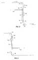
- FIG. 4is front elevational view of a panel of six arrays of UV LED assemblies shown in FIG. 3 in accordance with the teachings of the present invention and shows schematically a first eccentric cam which moves against one side edge of the panel against a spring at the opposite side edge of the panel so as to move, reciprocate or translate the panel in an X direction and a second eccentric cam which acts against an upper edge of the panel and against a spring bearing against a lower edge of the panel to cause movement of the panel in the Y direction and thereby cause all the arrays to move in a orbital, circular, or elliptical path when the first and second cams are rotated about their axes;
- FIG. 5is a block schematic diagram of a web made of, or carrying products, articles or other objects to be UV cured trained over rollers to move in a generally vertical path past the panel of arrays of UV LED assemblies shown in FIG. 4 such that the products, articles or other objects with UV photo initiators therein can be cured as each product, article or other object moves past the arrays of UV LED assemblies while a non-oxygen, heavier than air gas is injected from a gas tube located near the top of the path of movement of the web; and
- FIG. 6is a block schematic view of a web made of, or carrying, products, articles or other objects to be UV cured trained over rollers to move in a generally vertical path past the panel of arrays of UV LED assemblies shown in FIG. 4 such that each product, article or other object with UV photo initiators therein can be cured as each product, article or other object moves past the arrays of UV LED assemblies while a non-oxygen gas is injected from a gas tube located near the bottom of the path of movement of the web.
- FIG. 1a prior art ultraviolet light-emitting diode (UV LED) assembly 10 including a cathode pad 12 and an anode 14 mounting a chip 16 , which comprises a UV LED chip 16 .
- UV LEDultraviolet light-emitting diode
- Each cathode pad 12(FIG. 1) is connected to a wire conductor as is each anode 14 .
- FIG. 2there is illustrated therein a building block 20 having a first array 21 of the UV LED assemblies 10 thereon, namely, pads 12 and anodes 14 , which provide a plurality of UV LED chips 16 .
- the building block 20is designed to mate with similar building blocks to form a group 22 of arrays 21 , 23 and 25 as shown in FIG's 3 and 4 .
- several of the blocks 20can matingly engage each other and be arranged in a pattern (e.g. like tiles on a floor) on a panel 28 (FIG. 4).
- the UV LED assemblies 10 in each array 21 , 23 and 25are spaced apart in a first lower row 36 of UV LED assemblies 10 . Then, in a second adjacent row 38 , the UV LED assemblies 10 are arranged in a staggered manner so that they are located above the spaces between the UV LED assemblies 10 in the first row. In the same manner, the next upper row 40 of UV LED assemblies 10 is staggered and a total of twenty (20) staggered rows are provided in the UV LED array 21 shown in FIG. 3.
- the beginning of the first UV LED assembly 10 in the uppermost row 44 in the first array 21is aligned with the end of the last UV LED assembly 10 in the uppermost row 46 in the second, lower left array 23 .
- the end of the last UV LED assembly 10 in the lowest row 36 in the first array 21is aligned with the beginning of the first UV LED assembly 10 in the lowest row 48 in the third, lower right array 25 .
- the end of the last UV LED assembly 10 in the uppermost row 44 in the first array 21is aligned with the beginning of the first UV LED assembly 10 in the uppermost row 49 in the third, lower right array 25 , as shown in FIG. 3.
- the three arrays 21 , 23 and 25can be arranged on the panel 28 in a staggered manner so that the UV light from each UV LED assembly 10 is not only spaced and staggered relative to adjacent rows in the array but also spaced and staggered relative to the rows in the other arrays. Also more than three arrays 21 , 23 and 25 can be provided, such as six arrays, not shown.
- eccentric cams 50 and 52that can be provided for moving, translating or reciprocating the panel 28 back and forth in the X direction and up and down in the Y direction, much like in an orbital sander.
- the first, x axis, eccentric cam 50is mounted for rotation about a shaft 54 to act against one side edge 56 of the panel 28 with a spring 58 , such as a helical tension spring, positioned to act against the other side edge 60 of the panel 28 .
- the second, y axis, eccentric cam 52(FIG. 4) is mounted for rotation on a shaft 64 to act against an upper edge 66 of the panel 28 against the action of a spring 68 , such as a helical tension spring, positioned to act against a lower edge 70 of the panel 28 .
- a spring 68such as a helical tension spring
- Rotation of the shafts 54 and 64 (FIG. 4) each by a prime mover such as a variable speed motor (not shown)can cause the panel 28 to move in a generally orbital, annular, circular, or elliptical path of movement. This will result in orbital movement of each UV LED assembly 10 in each of the rows in each of the arrays 21 , 23 and 25 mounted on the panel 28 so as to spread out the emitted UV light and uniformly apply the UV light to the products, articles or other objects to be UV cured. This spreading of the UV light also minimizes, if not altogether eliminates the creation of, so called “hot spots” of UV light.
- the panel 28 of UV LED arrays 21 , 23 and 25is positioned generally vertically and closely adjacent the path of movement of a conveyor belt comprising web 74 which is trained over rollers 76 , 78 and 80 to move generally upright and vertically past and closely adjacent and in proximity to the panel of UV LED arrays 21 , 23 and 25 .
- a conveyor beltcomprising web 74 which is trained over rollers 76 , 78 and 80 to move generally upright and vertically past and closely adjacent and in proximity to the panel of UV LED arrays 21 , 23 and 25 .
- at least one of the rollers 76 , 78 and/or 80 of a conveyorcan be a drive roller.
- UV curable products, articles or other objects, such as labels, positioned in or on the web 74 (FIG. 5),can have one or more UV curable inks, coatings and/or adhesives between a plastic cover layer and the label.
- the UV curable ink, coating, and/or adhesivecan have UV photo initiators therein which will polymerize the monomers in the UV curable ink, coating, or adhesive when subjected to UV light within a predetermined UV wavelength range.
- the UV curable ink, coating and/or adhesiveis preferably located on the side of the web 74 (FIG. 5) that is closest to and faces the panel 28 .
- the spacing between the UV LED assemblies and the ink, coating or adhesiveis between 0.001 inch and 0.3 inch to enhance the effectiveness of the UV emitted light which dissipates exponentially as the distance to the product, article or other UV curable object to be treated increases.
- the shafts 50 and 52are rotated to cause orbital movement of the panel 28 and UV LED assemblies as the web 74 containing the product, article or other UV curable object moves past the panel 28 .
- Such movementalso minimizes “hot spots” and provide uniform sweeping, distribution, and application of the UV light from the UV LED assemblies 10 .
- FIG. 5The block schematic diagram of the assembly or device, shown in FIG. 5 is provided to minimize exposure of the products, articles or other objects during curing to oxygen, which inhibits UV curing.
- a gas tube 84 providing an upper gas injectionis provided on the assembly and device for injecting heavier-than-air, non-oxygen-containing gas, e.g., carbon dioxide, near an upper end 86 of a path of downward movement, indicated by the arrow 88 , of the web 74 , so that the gas can flow downwardly in the space between the panel 28 and the web 74 to provide an anaerobic area between the UV LED assemblies 10 on the panel 28 and the web 74 having UV curable products, articles or other objects to be cured.
- heavier-than-air, non-oxygen-containing gase.g., carbon dioxide
- a wiper blade 90(FIG. 5) providing a lower inhibitor go can be positioned adjacent the lower edge 70 of the panel 28 for holding, compressing, collecting and/or blanketing the gas in the area between the orbiting UV LED arrays 21 , 23 and 25 (FIG. 4) and the moving web 74 (FIG. 5).
- the wiper blade 90is fixed to the lower edge 70 of the panel 28 and has an outer edge 92 that is positioned to wipe against the moving web 74 . In this way, the injected gas can be inhibited from escaping the curing area.
- FIG. 6is a block schematic diagram of a UV curing apparatus, assembly, mechanism or device constructed according to the teachings of the present invention where the moving web 74 is trained about rollers 94 , 96 and 98 , at least one of which can be a drive roller, to cause the web 74 with the UV curable products, articles or other objects thereon or therein to move upwardly, as shown by the arrow 100 , past the panel 28 mounting arrays 21 , 23 and 25 (FIG. 4) of UV LED assemblies, much the same as in the UV curing apparatus, assembly and device shown in FIG. 5.
- a gas tube 104 providing a lower gas injectoris positioned near a lower end 106 of the path 100 of movement of the web 74 for injecting an inert lighter-than-air, non-oxygen-containing gas, e.g., helium, in the area between the orbiting panel 28 (FIG. 4) and the upwardly moving web 74 (FIG. 6) thereby provide an anaerobic area to enhance and facilitate curing of the UV photo initiators in the UV curable products, articles or other objects that are carried by the web 74 .
- an inert lighter-than-air, non-oxygen-containing gase.g., helium
- a wiper blade 108(FIG. 6) providing an upper inhibitor 108 is positioned near the upper edge 68 of the panel 28 as shown in FIG. 6 to minimize the escape of the lighter-than-air gas and hold, compress, collect and/or blanket the injected gas in the curing area between the orbiting panel 28 (FIG. 4) and the moving web 74 (FIG. 6), much the same as in the UV curing apparatus, assembly and device shown in FIG. 5.
- the wiper blade 108 (FIG. 6)can be fixed to the upper edge 68 and arranged to wipe against the web 74 .
- the power supplied to the UV LED assembliescan be periodically or sequentially activated and deactivated, i.e. can be turned on and off, at a relatively high frequency. Also, the duty cycle of the on-off cycle can be varied to adjust the UV light intensity.
- FIG. 7is illustrated another way to position the UV LED assemblies, namely, the LED chips 16 , and achieve the same uniformity as shown in FIGS. 2 and 3. This would be to use 3 rows to achieve the uniformity. That is, to have the LED chips 16 in a first row 112 arranged at a distance of X, and to have the next row 114 (row 2 ) start at a distance 1 ⁇ 3 in from the start of the first row 112 and the next row 116 (row 3 ) start at a distance 2 ⁇ 3 in from the start of the first row 112 or at a distance 1 ⁇ 3 in from the start of the second row 114 .
- the space Xcan be equal to the width of 1, 2, 3, 4, 5, etc. of an UV LED assembly 10 to provide a desired staggering of the light beams from the UV LED assemblies 10 .
- a clear/transparent sheet or layer of plastic materialcan be placed over the arrays 21 , 23 and 25 to protect the UV LED assemblies 10 . Then, the sheet or layer is cleaned or replaced periodically.
- the panel 28 of UV LED assemblies 10can be arranged closely adjacent the web 74 carrying UV curable products, articles or other objects which enables UV light from UV LED assemblies 10 to better effect curing of the UV curable ink, coating and/or adhesive.
- the moving of the web 74 , carrying the UV curable products, articles or other objects past staggered rows of UV LED assemblies 10 in staggered arrays 21 , 23 and 25 of UV LED assemblies 10 on the panel 28ensures uniform application of UV light to all of the ink, coating and/or adhesive to be cured in the UV curable product, article or object.
- the oscillating or orbital movement of the UV LED assemblies 10 adjacent the moving web containing the UV curable products, articles or other objects to be curedensures a more uniform sweeping of the UV light over the UV curable products, articles or other objects on or in the web 74 .
Landscapes
- Engineering & Computer Science (AREA)
- Mechanical Engineering (AREA)
- Life Sciences & Earth Sciences (AREA)
- Microbiology (AREA)
- General Engineering & Computer Science (AREA)
- Health & Medical Sciences (AREA)
- General Health & Medical Sciences (AREA)
- Toxicology (AREA)
- Application Of Or Painting With Fluid Materials (AREA)
- Coating Apparatus (AREA)
Abstract
Description
- 1. Field of the Invention[0001]
- The present invention relates to a method and apparatus for utilizing ultraviolet (UV) light emitting diodes in staggered arrays and mechanisms for moving the arrays to avoid “hot spots” and provide a uniform application of ultraviolet light to a moving object including inks, coatings or adhesives having UV photo initiators for converting, when exposed to UV light, monomers in the inks, coatings or adhesives to linking polymers to solidify the monomer material. Also, an inert, non-oxygen, gas is injected into the area where the staggered arrays of ultraviolet light emitting diodes, UV-LED's are positioned to apply UV light to the moving objects to enhance the curing of the ultraviolet activated UV photo initiators.[0002]
- 2. Description of the Prior Art[0003]
- Heretofore, ultraviolet lamps have been used for the curing of ultraviolet inks, coatings and adhesives.[0004]
- More recently, EXFO and EFOS of Mississauga, Ontario, Canada have developed UV light emitting diodes (LED's) and gathered them in large numbers for use in curing ultraviolet light sensitive monomers to polymerize the monomers and solidify the ink, coating or adhesive.[0005]
- While the use of a large number of UV-LED's provide many efficiencies, namely in cost and energy consumption, there is still the problem of effective curing with low intensity UV-LED's and with respect to “hot spots” which provide more curing at “hot spots” then at other locations in the ink, coating or adhesive being cured.[0006]
- Also, in the UV-LED prior art, the LED is positioned to achieve uniformity for back light displays and other lighting applications. The criteria for such uniformity are primarily designed to create an appearance that the backlight is uniform for a visual appearance.[0007]
- It is, therefore, desirable to provide an improved UV method and apparatus for applying UV light emitted from UV LED's more uniformly and avoid hot spots to more effectively cure UV inks, coatings and adhesives.[0008]
- As will be described in greater detail hereinafter, the method and device of the present invention provide techniques and structures for applying UV light emitted from UV-LED's more uniformly so that such light is more effective in curing inks, coatings and adhesives and, by applying the UV light more evenly, reducing, if not all together eliminating, “hot spots”.[0009]
- According to the present invention there is provided staggered arrays of UV LED assemblies on a panel with the UV LED assemblies being arranged in rows with each row being staggered from adjacent rows.[0010]
- In addition to the staggering of the UV LED assemblies in adjacent rows, a UV curable product, article or other object having a UV ink, coating or adhesive to be cured, is moved on or in a web past, and closely adjacent, the arrays.[0011]
- Further, the panel is moved or translated in an X direction and in a Y direction, much like an orbital sander, thereby to cause a slight sweeping of the light from each UV LED assembly over an orbital area, e.g., in a circular or elliptical pattern, thereby minimizing the creation of “hot spots” and to uniformly apply UV light to the product, article or other object having the UV ink, coating or adhesive.[0012]
- In one preferred embodiment, the web containing the UV curable product, article or other object to be cured is arranged to move vertically. A gas having a molecular weight heavier than air can be injected at the upper end of the path of movement of the UV curable product, article or other object having a UV ink, coating, or adhesive thereon as it moves past a panel of arrays of UV LED assemblies. Furthermore, a gas having a molecular weight lighter than air can be injected at the lower end of the path of movement of the UV curable product, article or other object having a UV ink, coating or adhesive thereon as it moves past the panel of arrays of UV LED assemblies.[0013]
- The method and apparatus of the present invention provide uniformity of light application from a flat panel having an array of UV-LED's. This result is obtained when the product and/or the light fixture is moved relative to and across the UV light beams from the UV-LED assemblies. This movement in of itself has the ability to offer one element of uniformity. That is, the movement of the product or the movement of the light array addresses the problem of providing uniformity in the direction of the product flow or of the lamp movement.[0014]
- The “X Axis” uniformity is addressed by the movement of the product or of the LED array.[0015]
- The “Y Axis” uniformity is addressed by how the LED chips are arranged. To achieve the cure rates that are associated with typical UV curing applications, a very large number of UV-LED chips are arranged to deliver, the amount of UV energy necessary to cure the polymers.[0016]
- The first step in building these arrays is to create either a series or parallel electrical circuit either in series or in which the LED chips are placed in a linear fashion of equal distance from each other. (Lets say a distance of X). The second row would start its row at a distance ½ X and each LED chip would then be spaced from adjacent LED chips in the row by the distance X.[0017]
- The third row would start at a distance ½ X in from the start of the second row. This offset would continue for each row of LED chips in the array. Two things happen when this is done. First the light uniformity is increased because of the alternating position of the UV-LED chips. This creates an overlap of light emissions. Then, having each row begin half the distance of the row it precedes will create a stair case effect. This will allow uniformity in the Y Axis as the array grows in size.[0018]
- There is another way to position the LED chips, and achieve the same uniformity. This would be to use 3 rows to achieve the uniformity. That is, to have the LED chips arranged at a distance of X, and to have the next row (row[0019]2) start at a distance ⅓ in from the start of the first row and the next row (row3) start at a distance ⅔ in from the start of the first row or at a distance ⅓ in from the start of the second row.
- Still another way is to provide 4 rows to create the uniformity, with the LED chips in the first row being spaced at a distance of X from each other. The second row starts its first LED chip at a distance ¼ X in from the first LED chip in the first row. The third row starts its row at a distance ½ X in from the first LED chip in the first row or at a distance ¼ X in from the start of the previous row.[0020]
- The method and apparatus of the present invention also address a very large number of LEDs that are mounted in long multiple rows, and still have a uniform distribution of light.[0021]
- Additionally, in situations where UV curable ink or adhesive may splatter onto the array of LED's, a thin transparent plastic sheet or layer is positioned over the array to protect the array, and the sheet or layer is periodically cleaned or replaced.[0022]
- A more detailed explanation of the invention is provided in the following detailed description and claims taken in conjunction with the accompanying drawings.[0023]
- FIG. 1 is a top plan elevational view of an UV LED assembly including a pad for a cathode and an anode mounting an UV LED chip in accordance with the teachings of the present invention;[0024]
- FIG. 2 is a top plan elevational view of a design of mating building blocks or substrates which can be blank or have an anode and cathode mounted thereon in accordance with the teachings of the present invention;[0025]
- FIG. 3 is a front elevational view of one array of UV LED assemblies wherein rows of UV LED assemblies are arranged in the array with alternate rows of UV LED assemblies in one row being staggered from the UV LED assemblies in the adjacent rows in accordance with the teachings of the present invention;[0026]
- FIG. 4 is front elevational view of a panel of six arrays of UV LED assemblies shown in FIG. 3 in accordance with the teachings of the present invention and shows schematically a first eccentric cam which moves against one side edge of the panel against a spring at the opposite side edge of the panel so as to move, reciprocate or translate the panel in an X direction and a second eccentric cam which acts against an upper edge of the panel and against a spring bearing against a lower edge of the panel to cause movement of the panel in the Y direction and thereby cause all the arrays to move in a orbital, circular, or elliptical path when the first and second cams are rotated about their axes;[0027]
- FIG. 5 is a block schematic diagram of a web made of, or carrying products, articles or other objects to be UV cured trained over rollers to move in a generally vertical path past the panel of arrays of UV LED assemblies shown in FIG. 4 such that the products, articles or other objects with UV photo initiators therein can be cured as each product, article or other object moves past the arrays of UV LED assemblies while a non-oxygen, heavier than air gas is injected from a gas tube located near the top of the path of movement of the web; and[0028]
- FIG. 6 is a block schematic view of a web made of, or carrying, products, articles or other objects to be UV cured trained over rollers to move in a generally vertical path past the panel of arrays of UV LED assemblies shown in FIG. 4 such that each product, article or other object with UV photo initiators therein can be cured as each product, article or other object moves past the arrays of UV LED assemblies while a non-oxygen gas is injected from a gas tube located near the bottom of the path of movement of the web.[0029]
- A detailed description of the preferred embodiments and best modes for practicing the invention are described herein.[0030]
- Referring now to the drawings in greater detail, there is illustrated in FIG. 1 a prior art ultraviolet light-emitting diode (UV LED)[0031]
assembly 10 including acathode pad 12 and ananode 14 mounting achip 16, which comprises aUV LED chip 16. - Each cathode pad[0032]12 (FIG. 1) is connected to a wire conductor as is each
anode 14. - Referring now to FIG. 2, there is illustrated therein a[0033]
building block 20 having afirst array 21 of theUV LED assemblies 10 thereon, namely,pads 12 andanodes 14, which provide a plurality ofUV LED chips 16. Thebuilding block 20 is designed to mate with similar building blocks to form agroup 22 ofarrays blocks 20 can matingly engage each other and be arranged in a pattern (e.g. like tiles on a floor) on a panel28 (FIG. 4). - As shown in FIG. 3, the[0034]
UV LED assemblies 10 in eacharray UV LED assemblies 10. Then, in a second adjacent row38, theUV LED assemblies 10 are arranged in a staggered manner so that they are located above the spaces between theUV LED assemblies 10 in the first row. In the same manner, the nextupper row 40 ofUV LED assemblies 10 is staggered and a total of twenty (20) staggered rows are provided in theUV LED array 21 shown in FIG. 3. - Also, as shown in FIG. 3 the beginning of the first[0035]
UV LED assembly 10 in the lowest row36 in thefirst array 21 is aligned with the end of the lastUV LED assembly 10 at the end of thelowest row 42 in the second, lower left,array 23. - Then,the beginning of the first[0036]
UV LED assembly 10 in theuppermost row 44 in thefirst array 21 is aligned with the end of the lastUV LED assembly 10 in theuppermost row 46 in the second, lowerleft array 23. Next, the end of the lastUV LED assembly 10 in the lowest row36 in thefirst array 21 is aligned with the beginning of the firstUV LED assembly 10 in thelowest row 48 in the third, lowerright array 25. Finally, the end of the lastUV LED assembly 10 in theuppermost row 44 in thefirst array 21 is aligned with the beginning of the firstUV LED assembly 10 in theuppermost row 49 in the third, lowerright array 25, as shown in FIG. 3. - As shown best in FIG. 4, the three[0037]
arrays panel 28 in a staggered manner so that the UV light from eachUV LED assembly 10 is not only spaced and staggered relative to adjacent rows in the array but also spaced and staggered relative to the rows in the other arrays. Also more than threearrays - Also shown in FIG. 4, are mechanisms, preferably[0038]
eccentric cams panel 28 back and forth in the X direction and up and down in the Y direction, much like in an orbital sander. The first, x axis,eccentric cam 50 is mounted for rotation about ashaft 54 to act against oneside edge 56 of thepanel 28 with aspring 58, such as a helical tension spring, positioned to act against theother side edge 60 of thepanel 28. - Then the second, y axis, eccentric cam[0039]52 (FIG. 4) is mounted for rotation on a
shaft 64 to act against anupper edge 66 of thepanel 28 against the action of aspring 68, such as a helical tension spring, positioned to act against alower edge 70 of thepanel 28. - Rotation of the[0040]
shafts 54 and64 (FIG. 4) each by a prime mover such as a variable speed motor (not shown) can cause thepanel 28 to move in a generally orbital, annular, circular, or elliptical path of movement. This will result in orbital movement of eachUV LED assembly 10 in each of the rows in each of thearrays panel 28 so as to spread out the emitted UV light and uniformly apply the UV light to the products, articles or other objects to be UV cured. This spreading of the UV light also minimizes, if not altogether eliminates the creation of, so called “hot spots” of UV light. - As shown in FIG. 5, where a schematic block diagram of one UV curing apparatus, assembly, mechanism or device constructed according to the teachings of the present invention is shown, the[0041]
panel 28 ofUV LED arrays belt comprising web 74 which is trained overrollers UV LED arrays rollers - UV curable products, articles or other objects, such as labels, positioned in or on the web[0042]74 (FIG. 5), can have one or more UV curable inks, coatings and/or adhesives between a plastic cover layer and the label. The UV curable ink, coating, and/or adhesive can have UV photo initiators therein which will polymerize the monomers in the UV curable ink, coating, or adhesive when subjected to UV light within a predetermined UV wavelength range.
- The UV curable ink, coating and/or adhesive is preferably located on the side of the web[0043]74 (FIG. 5) that is closest to and faces the
panel 28. Preferably, the spacing between the UV LED assemblies and the ink, coating or adhesive is between 0.001 inch and 0.3 inch to enhance the effectiveness of the UV emitted light which dissipates exponentially as the distance to the product, article or other UV curable object to be treated increases. - Preferably, the[0044]
shafts 50 and52 (FIG. 4) are rotated to cause orbital movement of thepanel 28 and UV LED assemblies as theweb 74 containing the product, article or other UV curable object moves past thepanel 28. Such movement also minimizes “hot spots” and provide uniform sweeping, distribution, and application of the UV light from theUV LED assemblies 10. - The block schematic diagram of the assembly or device, shown in FIG. 5 is provided to minimize exposure of the products, articles or other objects during curing to oxygen, which inhibits UV curing. A[0045]
gas tube 84 providing an upper gas injection is provided on the assembly and device for injecting heavier-than-air, non-oxygen-containing gas, e.g., carbon dioxide, near anupper end 86 of a path of downward movement, indicated by thearrow 88, of theweb 74, so that the gas can flow downwardly in the space between thepanel 28 and theweb 74 to provide an anaerobic area between theUV LED assemblies 10 on thepanel 28 and theweb 74 having UV curable products, articles or other objects to be cured. - A wiper blade[0046]90 (FIG. 5) providing a lower inhibitor go can be positioned adjacent the
lower edge 70 of thepanel 28 for holding, compressing, collecting and/or blanketing the gas in the area between the orbitingUV LED arrays wiper blade 90 is fixed to thelower edge 70 of thepanel 28 and has anouter edge 92 that is positioned to wipe against the movingweb 74. In this way, the injected gas can be inhibited from escaping the curing area. - FIG. 6 is a block schematic diagram of a UV curing apparatus, assembly, mechanism or device constructed according to the teachings of the present invention where the moving[0047]
web 74 is trained aboutrollers web 74 with the UV curable products, articles or other objects thereon or therein to move upwardly, as shown by thearrow 100, past thepanel 28 mountingarrays - In the apparatus, assembly or device shown in FIG. 6, a[0048]
gas tube 104 providing a lower gas injector is positioned near a lower end106 of thepath 100 of movement of theweb 74 for injecting an inert lighter-than-air, non-oxygen-containing gas, e.g., helium, in the area between the orbiting panel28 (FIG. 4) and the upwardly moving web74 (FIG. 6) thereby provide an anaerobic area to enhance and facilitate curing of the UV photo initiators in the UV curable products, articles or other objects that are carried by theweb 74. - A wiper blade[0049]108 (FIG. 6) providing an
upper inhibitor 108 is positioned near theupper edge 68 of thepanel 28 as shown in FIG. 6 to minimize the escape of the lighter-than-air gas and hold, compress, collect and/or blanket the injected gas in the curing area between the orbiting panel28 (FIG. 4) and the moving web74 (FIG. 6), much the same as in the UV curing apparatus, assembly and device shown in FIG. 5. Again, the wiper blade108 (FIG. 6) can be fixed to theupper edge 68 and arranged to wipe against theweb 74. - To avoid overheating the[0050]
UV LED assemblies 10, i.e., to control the heat generated by theUV LED assemblies 10, the power supplied to the UV LED assemblies can be periodically or sequentially activated and deactivated, i.e. can be turned on and off, at a relatively high frequency. Also, the duty cycle of the on-off cycle can be varied to adjust the UV light intensity. - In FIG. 7 is illustrated another way to position the UV LED assemblies, namely, the LED chips[0051]16, and achieve the same uniformity as shown in FIGS. 2 and 3. This would be to use 3 rows to achieve the uniformity. That is, to have the LED chips16 in a
first row 112 arranged at a distance of X, and to have the next row114 (row2) start at a distance ⅓ in from the start of thefirst row 112 and the next row116 (row3) start at a distance ⅔ in from the start of thefirst row 112 or at a distance ⅓ in from the start of thesecond row 114. - It will be understood that the space X can be equal to the width of 1, 2, 3, 4, 5, etc. of an[0052]
UV LED assembly 10 to provide a desired staggering of the light beams from theUV LED assemblies 10. - Also, in situations where UV curable ink or adhesive might splatter on the[0053]
UV LED assemblies 10, a clear/transparent sheet or layer of plastic material can be placed over thearrays UV LED assemblies 10. Then, the sheet or layer is cleaned or replaced periodically. - From the foregoing description it will be apparent that the method and device of the present invention have a number of advantages, some of which have been described above and others of which are inherent in the invention. For example, the[0054]
panel 28 ofUV LED assemblies 10 can be arranged closely adjacent theweb 74 carrying UV curable products, articles or other objects which enables UV light fromUV LED assemblies 10 to better effect curing of the UV curable ink, coating and/or adhesive. - Further, the moving of the[0055]
web 74, carrying the UV curable products, articles or other objects past staggered rows ofUV LED assemblies 10 instaggered arrays UV LED assemblies 10 on thepanel 28 ensures uniform application of UV light to all of the ink, coating and/or adhesive to be cured in the UV curable product, article or object. - Still further, the oscillating or orbital movement of the[0056]
UV LED assemblies 10 adjacent the moving web containing the UV curable products, articles or other objects to be cured ensures a more uniform sweeping of the UV light over the UV curable products, articles or other objects on or in theweb 74. - Finally, the application of a heavier-than-air or a lighter-than-air, non-oxygen-containing gas to the area between the oscillating or orbiting[0057]
panel 28 ofUV LED assemblies 10 and theweb 74 carrying the UV curable products, articles or other objects having monomer material to be cured or polymerized enhances the emission and application of more uniform UV light upon the UV curable products, articles, or other objects. - Although embodiments of the invention have been shown and described, it will be understood that various modifications and substitutions, as well as rearrangements of components, parts, equipment, apparatus, process (method) steps, and uses thereof, can be made by those skilled in the art without departing from the teachings of the invention. Accordingly, the scope of the invention is only to be limited as necessitated by the accompanying claims.[0058]
Claims (52)
1. A method for enhancing the application of UV light to UV photo initiators in a UV curable ink, coating or adhesive on or in a UV curable product, article or other object, comprising the steps of:
arranging an array of UV LED assemblies in a first row with the UV LED assemblies spaced from adjacent UV LED assemblies;
arranging at least one second row of a plurality of UV LED assemblies next to the first row but with the UV LED assemblies of the second row positioned adjacent the spaces between adjacent UV LED assemblies in the first row thereby to stagger the second row of UV LED assemblies from the UV LED assemblies in the first row;
mounting at least the first and second rows of staggered UV LED assemblies on a panel; and,
moving UV curable products, articles or other objects containing UV photo initiators that are in or on a web past the at least two rows of UV LED assemblies, the staggering of the UV LED assemblies facilitating a substantially uniform application of UV light on the UV curable ink, coating or adhesive of said UV curable products, articles or other objects.
2. The method ofclaim 1 , including more than two staggered rows of UV LED assemblies are provided to form a staggered array of UV LED assemblies mounted on the panel.
3. The method ofclaim 2 , wherein six arrays of UV LED assemblies are mounted in a staggered manner on the panel.
4. The method ofclaim 2 , wherein the UV-LED assemblies in each row are spaced a distance X from each other and the first UV-LED assembly in the second row starts the second row at a distance ½ X in from the first UV-LED assembly in the first row and the UV-LED assemblies in the second row are spaced from each other by the distance X and the first UV-LED assembly in a third row starts at a distance ½ X in from the start of the second row.
5. The method ofclaim 2 , wherein the UV-LED assemblies in each row are spaced a distance X from each other and the first UV-LED assembly in the second row starts the second row at a distance ⅓ in from the first UV-LED assembly in the first row and the first UV-LED assembly in the next or third row starts at a distance ⅔ in from the first UV-LED assembly in the first row or at a distance ⅓ in from the first UV-LED assembly in the second row.
6. The method ofclaim 2 , wherein the UV-LED assemblies in each row are spaced a distance X from each other and the first UV-LED assembly in the second row starts the second row at a distance ¼ X in from the first UV-LED assembly in the first row and a first UV-LED assembly in a third row starts its row at a distance ½ X in from the start of the first row or at a distance ¼ X in from the start of the second row.
7. The method ofclaim 1 , wherein said panel is mounted closely adjacent one side of the web so that the distance between the ultraviolet (UV) light emitted and the UV initiators in the adhesive or ink coating is between approximately 0.001 inch and 0.3 inch.
8. The method ofclaim 1 including the step of training the web over rollers to move the web in a generally vertical path past the staggered UV LED assemblies.
9. The method ofclaim 8 including the step of injecting a non-oxygen-containing, lighter-than-air gas at a lower end of the path of movement of the web past the panel of staggered arrays of light emitting diodes (LED) thereby further to facilitate curing of the UV initiators in the UV curable ink, coating or adhesive on or in the UV curable product, article or other object and said non-oxygen-containing gas having a molecular weight less than air.
10. The method ofclaim 9 wherein said gas is helium.
11. The method ofclaim 9 , including the step of substantially inhibiting exit flow of the gas at the upper end of the panel.
12. The method ofclaim 11 wherein said step of inhibiting is accomplished by mounting a wiper blade adjacent the upper end of the panel between the panel and the moving web.
13. The method ofclaim 8 , including the step of injecting a non-oxygen-containing, heavier-than-air gas near the upper end of the generally vertical path of the web thereby to facilitate further the curing of the UV initiators in the UV curable ink, coating or adhesive on or in the UV curable product, article or other object and said non-oxygen-containing gas having a molecular weight greater than air.
14. The method ofclaim 13 wherein said gas is carbon dioxide.
15. The method ofclaim 13 , including the step of substantially inhibiting exit flow of the gas at the lower end of the panel.
16. The method ofclaim 15 wherein said step of inhibiting is accomplished by mounting a wiper blade adjacent the upper end of the panel between the panel and the moving web.
17. The method ofclaim 1 , including the step of moving the panel in at least one of the X, Y axes thereby to apply UV light substantially uniformly over the UV curable product, article or object on the moving web to minimize substantially any “hot spots”.
18. The method ofclaim 17 , including the step of moving the panel in both an X axis reciprocal path and a Y axis reciprocal path to move or oscillate the panel in an orbital, annular, circular or elliptical path as the web carrying the UV curable products, articles or other objects is moved past the panel.
19. The method ofclaim 1 including the step of placing a thin, transparent plastic sheet or layer over the array to protect the UV LED assemblies from splatter of UV curable ink or adhesive.
20. The method ofclaim 19 including the step of periodically cleaning or replacing the sheet or layer of transparent plastic material.
21. A UV curing apparatus having a light emitting device for applying UV light to UV photo initiators in a UV curable ink, coating, or adhesive on or in a UV curable products, article or other object, comprising:
a set of UV LED assemblies arranged on a panel in a first row with the UV LED assemblies spaced from adjacent UV LED assemblies;
at least one second row of a plurality of UV LED assemblies arranged on the panel next to the first row but with the UV LED assemblies of the second row positioned adjacent the spaces between adjacent UV LED assemblies in the first row thereby to stagger the second row of UV LED assemblies relative to the UV LED assemblies in the first row; and
a moveable assembly comprising a web for moving the UV curable products, articles or other objects containing UV photo initiators past the at least two rows of UV LED assemblies, the staggering of the UV LED assemblies facilitating substantial uniform application of UV light on the UV curable ink, coating or adhesive on or in the UV curable products, articles or other objects.
22. The apparatus ofclaim 21 , comprising more than two staggered rows of UV LED assemblies on the panel to form a staggered array of UV LED assemblies on the panel.
23. The apparatus ofclaim 22 , wherein the UV-LED assemblies in each row are spaced a distance X from each other and the first UV-LED assembly in the second row starts the second row at a distance ½ X in from the first UV-LED assembly in the first row and the UV-LED assemblies in the second row are spaced from each other by the distance X and the first UV-LED assembly in a third row starts at a distance ½ X in from the start of the second row.
24. The apparatus ofclaim 22 , wherein the UV-LED assemblies in each row are spaced a distance X from each other and the first UV-LED assembly in the second row starts the second row at a distance ⅓ in from the first UV-LED assembly in the first row and the first UV-LED assembly in the next or third row starts at a distance ⅔ in from the first UV-LED assembly in the first row or at a distance ⅓ in from the first UV-LED assembly in the second row.
25. The apparatus ofclaim 22 , wherein the UV-LED assemblies in each row are spaced a distance X from each other and the first UV-LED assembly in the second row starts the second row at a distance ¼ X in from the first UV-LED assembly in the first row and a first UV-LED assembly in a third row starts its row at a distance ½ X in from the start of the first row or at a distance ¼ X in from the start of the second row.
26. The apparatus ofclaim 22 , wherein six arrays of staggered UV LED assemblies are mounted in a staggered manner on the panel.
27. The apparatus ofclaim 21 , wherein said panel is mounted closely adjacent one side of the web so that the distance between the ultraviolet (UV) light emitted and the UV initiators in the adhesive or ink coating is between approximately 0.001 inch and 0.3 inch.
28. The apparatus ofclaim 21 , wherein said web is trained over rollers to move the web in a generally vertical path past the staggered UV LED assemblies.
29. The apparatus ofclaim 28 , including a lower gas injector for injecting a non-oxygen, lighter-than-air gas at a lower end of the path of movement of the web past the panel of staggered arrays of light emitting diodes (LED) thereby further to facilitate curing of the UV initiators in the UV curable ink, coating or adhesive.
30. The apparatus ofclaim 29 wherein said gas is helium.
31. The apparatus ofclaim 30 , including an upper inhibitor for substantially inhibiting exit flow of the gas at the upper end of the panel.
32. The apparatus ofclaim 31 wherein said upper inhibitor includes a wiper blade mounted adjacent the upper end of the panel between the panel and the moving web.
33. The apparatus ofclaim 28 , including an upper gas injector for injecting a non-oxygen, heavier-than-air gas in proximity to the upper end of the generally vertical path of the web to facilitate curing of the UV initiators in the UV curable ink, coating or adhesive.
34. The apparatus ofclaim 33 wherein said gas is carbon dioxide.
35. The apparatus ofclaim 33 , including a lower inhibitor for substantially inhibiting exit flow of the gas at the lower end of the panel.
36. The apparatus ofclaim 35 wherein said lower inhibitor includes a wiper blade mounted adjacent the upper end of the panel between the panel and the moving web.
37. The apparatus ofclaim 21 wherein said moveable assembly includes a mechanism for moving the panel in at least one of the X, Y axes thereby to apply UV light substantially uniformly over the UV curable product, article or other object on or in the moving web to substantially minimize “hot spots.
38. The apparatus ofclaim 37 , wherein said mechanism comprises an orbiting mechanism for moving the panel in both an X axis reciprocal path and a Y axis reciprocal path thereby to move the panel in an orbital, annular, circular or elliptical path as the web carrying UV curable products, article or other objects conveyed past the panel.
39. The apparatus ofclaim 37 wherein said mechanism includes a spring mounted adjacent one side of said panel, a cam eccentrically mounted adjacent the other side of said panel, on a shaft, and a driver for rotating said shaft thereby to rotate said cam and move said panel in a reciprocal path against said spring.
40. The apparatus ofclaim 21 including a thin, transparent sheet or layer of plastic material over the UV LED assemblies on the panel to protect the UV LED assemblies from splatter of UV curable ink or adhesive.
41. A method for enhancing the application of UV light to UV photo initiators in a UV curable ink, coating or adhesive on or in a UV curable product, article or other object, comprising the steps of:
arranging an array of UV LED assemblies on a panel;
moving the UV curable products, articles or other objects containing UV photo initiators, that are in or on a web, past the array of LED assemblies; and,
moving the panel containing the array of LED assemblies in an orbital, annular, circular or elliptical path as the web carrying the UV curable product, article or other object is moved past the panel.
42. A method for enhancing the application of UV light to UV photo initiators in a UV curable ink, coating or adhesive on or in a UV curable product, article or other object, comprising the steps of:
arranging an array of UV LED assemblies on a panel;
moving the UV curable products, articles or other objects containing UV photo initiators, that are in or on a web, past the array of LED assemblies; and
reciprocally moving the panel thereby to reciprocally sweep UV light across the panel substantially to apply UV curable light uniformly across the UV curable product, article or object substantially to minimize “hot spots”.
43. The method ofclaim 42 , including the step of reciprocally moving the panel in both an X axis reciprocal path and a Y axis reciprocal path to move or oscillate the panel in a generally orbital, annular, circular or elliptical path as the web, carrying the UV curable products, articles, or other objects, is moved past the panel.
44. A method for enhancing curing with a UV light applied to UV photo initiators in a UV curable ink, coating or adhesive in a UV curable product, article or other object in or on a web, comprising the steps of:
arranging an array of UV LED assemblies on a panel;
positioning the panel closely adjacent a generally vertical path of movement of a web carrying the UV curable products, articles or other objects; and,
curing said UV curable product, article or other object by
emitting UV light on the UV photo initiators;
polymerizing said UV curable ink, coating, or adhesive; and,
minimizing exposure of said UV curable ink, coating or adhesive to oxygen during polymerization by injecting a lighter than air gas at the lower end of the path of movement of the web past the panel having the array of LED assemblies during said curing.
45. A method for enhancing curing with a UV light applied to UV photo initiators in a UV curable ink, coating or adhesive in a UV curable product, article or other object in or on a web comprising the steps of:
arranging an array of UV LED assemblies on a panel;
positioning the panel closely adjacent a generally vertical path of movement of a web carrying the UV curable products, articles or other objects; and,
curing said UV curable product, article or other object by
emitting UV light on the UV photo initiators;
polymerizing said UV curable ink, coating, or adhesive; and,
minimizing exposure of said UV curable ink, coating or adhesive to oxygen during polymerization by injecting a lighter than air gas at the lower end of the path of movement of the web past the panel having the array of LED assemblies during said polymerizing.
46. An apparatus for enhancing the application of UV light to UV photo initiators in a UV curable ink, coating or adhesive on or in a UV curable product, article or other object, comprising:
a conveyor having a web and roller assemblies for moving said web, said web carrying or containing UV curable products, articles or other objects;
an array of UV LED assemblies on a panel, said panel being positioned adjacent the moving web; and,
a mechanism comprising an oscillator for moving the panel containing the array of LED assemblies in an orbital, annular, circular or elliptical path as the web carrying the UV curable product, article or other object moves past the panel.
47. An apparatus for enhancing the application of UV light to UV photo initiators in a UV curable ink, coating or adhesive on or in a UV curable product, article or other object, comprising:
a conveyor having a conveyor belt comprising web roller assemblies for moving said web, said web carrying or containing UV curable products, articles or other objects on or in the web;
an array of UV LED assemblies on a panel, said panel being positioned adjacent the moving web; and,
a reciprocating mechanism for moving the panel containing the array of LED assemblies in a reciprocal path as the web carrying the UV curable product, article or other object moves past the panel.
48. The apparatus ofclaim 47 , wherein said mechanism includes an eccentric cam acting against one side of the panel and against a spring acting against the other side of the panel.
49. The apparatus ofclaim 47 wherein said mechanism includes a first eccentric cam acting against one side of the panel and against a spring acting against the other side of the panel and a second eccentric cam acting against another side of the panel and against a spring acting against the side opposite said another side of the panel to reciprocally move the panel in both an X axis reciprocal path and a Y axis reciprocal path to move or oscillate the panel in a generally orbital, annular, circular or elliptical path as the web carrying the UV curable products, articles, or other objects is moved past the panel.
50. An apparatus for enhancing curing with a UV light applied to UV photo initiators in a UV curable ink; coating or adhesive in a UV curable product, article or other object in or on a web, comprising:
a conveyor having a conveyor belt comprising a web and roller assemblies for moving the web, said web carrying or containing UV curable products, articles or other objects through a path including a generally vertical path section;
an array of UV LED assemblies mounted on a panel, said panel being positioned closely adjacent the generally vertical path section; and,
a lower injector for injecting a lighter-than-air, non-oxygen gas at the lower end of the generally vertical path section of the web to create a substantially anaerobic area during curing of the UV curable ink, coating or adhesive.
51. An apparatus for enhancing curing with a UV light applied to UV photo initiators in a UV curable ink, coating or adhesive in a UV curable product, article or other object in or on a web comprising:
a conveyor having a web and roller assemblies for moving said web, said web carrying or containing UV curable products, articles or other objects through a path including a generally vertical path section;
an array of UV LED assemblies mounted on a panel, said panel being positioned in close proximity to the generally vertical path section; and,
an upper injector for injecting a heavier-than-air, non-oxygen gas at the upper end of the generally vertical path section of the web to create a substantially anaerobic area between the panel and the moving web during curing of the UV curable ink, coating or adhesive.
52. The apparatus ofclaim 47 including a thin, transparent sheet or layer of plastic material over the UV LED assemblies on the panel to protect the UV LED assemblies from splatter of UV curable ink or adhesive.
Priority Applications (14)
| Application Number | Priority Date | Filing Date | Title |
|---|---|---|---|
| US10/339,264US7175712B2 (en) | 2003-01-09 | 2003-01-09 | Light emitting apparatus and method for curing inks, coatings and adhesives |
| US10/386,980US20060121208A1 (en) | 2003-01-09 | 2003-03-12 | Multiple wavelength UV curing |
| US10/753,837US20050042390A1 (en) | 2003-01-09 | 2004-01-07 | Rotary UV curing method and apparatus |
| US10/753,947US7211299B2 (en) | 2003-01-09 | 2004-01-07 | UV curing method and apparatus |
| US10/789,020US20040164325A1 (en) | 2003-01-09 | 2004-02-20 | UV curing for ink jet printer |
| US10/886,332US7465909B2 (en) | 2003-01-09 | 2004-07-07 | UV LED control loop and controller for causing emitting UV light at a much greater intensity for UV curing |
| US11/017,354US7137696B2 (en) | 2003-01-09 | 2004-12-20 | Ink jet UV curing |
| US10/907,180US7498065B2 (en) | 2003-01-09 | 2005-03-23 | UV printing and curing of CDs, DVDs, Golf Balls And Other Products |
| US10/908,651US7399982B2 (en) | 2003-01-09 | 2005-05-20 | UV curing system and process with increased light intensity |
| US11/342,165US7671346B2 (en) | 2003-01-09 | 2006-01-27 | Light emitting apparatus and method for curing inks, coatings and adhesives |
| US11/361,902US20060204670A1 (en) | 2003-01-09 | 2006-02-24 | UV curing method and apparatus |
| US11/561,843US20070139504A1 (en) | 2003-01-09 | 2006-11-20 | Ink Jet UV Curing |
| US12/050,616US20080160211A1 (en) | 2003-01-09 | 2008-03-18 | Rotary UV Curing Method and Apparatus |
| US12/762,916US20100242299A1 (en) | 2003-01-09 | 2010-04-19 | Uv curing system and process |
Applications Claiming Priority (1)
| Application Number | Priority Date | Filing Date | Title |
|---|---|---|---|
| US10/339,264US7175712B2 (en) | 2003-01-09 | 2003-01-09 | Light emitting apparatus and method for curing inks, coatings and adhesives |
Related Child Applications (10)
| Application Number | Title | Priority Date | Filing Date |
|---|---|---|---|
| US10/386,980Continuation-In-PartUS20060121208A1 (en) | 2003-01-09 | 2003-03-12 | Multiple wavelength UV curing |
| US10/753,947Continuation-In-PartUS7211299B2 (en) | 2003-01-09 | 2004-01-07 | UV curing method and apparatus |
| US10/753,837Continuation-In-PartUS20050042390A1 (en) | 2003-01-09 | 2004-01-07 | Rotary UV curing method and apparatus |
| US10/789,020Continuation-In-PartUS20040164325A1 (en) | 2003-01-09 | 2004-02-20 | UV curing for ink jet printer |
| US10/886,332Continuation-In-PartUS7465909B2 (en) | 2003-01-09 | 2004-07-07 | UV LED control loop and controller for causing emitting UV light at a much greater intensity for UV curing |
| US11/017,354Continuation-In-PartUS7137696B2 (en) | 2003-01-09 | 2004-12-20 | Ink jet UV curing |
| US10/907,180Continuation-In-PartUS7498065B2 (en) | 2003-01-09 | 2005-03-23 | UV printing and curing of CDs, DVDs, Golf Balls And Other Products |
| US10/908,651Continuation-In-PartUS7399982B2 (en) | 2003-01-09 | 2005-05-20 | UV curing system and process with increased light intensity |
| US11/342,165Continuation-In-PartUS7671346B2 (en) | 2003-01-09 | 2006-01-27 | Light emitting apparatus and method for curing inks, coatings and adhesives |
| US11/361,902Continuation-In-PartUS20060204670A1 (en) | 2003-01-09 | 2006-02-24 | UV curing method and apparatus |
Publications (2)
| Publication Number | Publication Date |
|---|---|
| US20040135159A1true US20040135159A1 (en) | 2004-07-15 |
| US7175712B2 US7175712B2 (en) | 2007-02-13 |
Family
ID=32711076
Family Applications (1)
| Application Number | Title | Priority Date | Filing Date |
|---|---|---|---|
| US10/339,264Expired - Fee RelatedUS7175712B2 (en) | 2003-01-09 | 2003-01-09 | Light emitting apparatus and method for curing inks, coatings and adhesives |
Country Status (1)
| Country | Link |
|---|---|
| US (1) | US7175712B2 (en) |
Cited By (81)
| Publication number | Priority date | Publication date | Assignee | Title |
|---|---|---|---|---|
| US20040238111A1 (en)* | 2003-01-09 | 2004-12-02 | Con-Trol-Cure, Inc. | UV LED control loop and controller for UV curing |
| US20050023488A1 (en)* | 2003-06-04 | 2005-02-03 | Kazumitsu Katsuki | Ultraviolet irradiating device |
| US20050154075A1 (en)* | 2003-01-09 | 2005-07-14 | Con-Trol-Cure, Inc. | UV Printing And Curing of CDs, DVDs, Golf Balls And Other Products |
| US20050222295A1 (en)* | 2003-01-09 | 2005-10-06 | Con-Trol-Cure, Inc. | UV Curing System and Process with Increased Light Intensity |
| US20050230600A1 (en)* | 2004-03-30 | 2005-10-20 | Olson Steven J | LED array having array-based LED detectors |
| US20050231713A1 (en)* | 2004-04-19 | 2005-10-20 | Owen Mark D | Imaging semiconductor structures using solid state illumination |
| US20050280683A1 (en)* | 2005-09-20 | 2005-12-22 | Custer Eric J | Ultraviolet light-emitting diode device |
| US20060119686A1 (en)* | 2004-12-07 | 2006-06-08 | Xerox Corporation | Apparatus and process for printing ultraviolet curable inks |
| US20060127594A1 (en)* | 2003-01-09 | 2006-06-15 | Con-Trol-Cure, Inc. | Light emitting apparatus and method for curing inks, coatings and adhesives |
| US20060204670A1 (en)* | 2003-01-09 | 2006-09-14 | Con-Trol-Cure, Inc. | UV curing method and apparatus |
| US20060216865A1 (en)* | 2004-03-18 | 2006-09-28 | Phoseon Technology, Inc. | Direct cooling of leds |
| US20060233501A1 (en)* | 2003-03-01 | 2006-10-19 | Clayton Sampson | Ultraviolet curing |
| US20070030678A1 (en)* | 2003-10-31 | 2007-02-08 | Phoseon Technology, Inc. | Series wiring of highly reliable light sources |
| US20070051964A1 (en)* | 2004-04-12 | 2007-03-08 | Owen Mark D | High density led array |
| US20070109790A1 (en)* | 2003-10-31 | 2007-05-17 | Phoseon Technology, Inc. | Collection optics for led array with offset hemispherical or faceted surfaces |
| US20070139504A1 (en)* | 2003-01-09 | 2007-06-21 | Con-Trol-Cure, Inc. | Ink Jet UV Curing |
| US20070154823A1 (en)* | 2005-12-30 | 2007-07-05 | Phoseon Technology, Inc. | Multi-attribute light effects for use in curing and other applications involving photoreactions and processing |
| US20070184141A1 (en)* | 2005-09-20 | 2007-08-09 | Summit Business Products, Inc. | Ultraviolet light-emitting diode device |
| US20080282974A1 (en)* | 2007-05-15 | 2008-11-20 | Komori Corporation | Liquid curing apparatus for liquid transfer device |
| US7461949B2 (en) | 2002-05-08 | 2008-12-09 | Phoseon Technology, Inc. | Methods and systems relating to solid state light sources for use in industrial processes |
| US20090160923A1 (en)* | 2007-12-20 | 2009-06-25 | Summit Business Products, Inc. | Concentrated energy source |
| WO2009063134A3 (en)* | 2007-11-12 | 2009-07-23 | Tikkurila Oy | Coating an object |
| WO2009131490A3 (en)* | 2008-04-22 | 2009-12-17 | Mirchev Vladislav Yurievich | Method for curing substances by uv radiation, device for carrying out said method and ink cured by uv radiation |
| US7638808B2 (en) | 2004-03-18 | 2009-12-29 | Phoseon Technology, Inc. | Micro-reflectors on a substrate for high-density LED array |
| US20100039806A1 (en)* | 2005-11-18 | 2010-02-18 | Cree, Inc. | Led lighting units and assemblies with edge connectors |
| US20100130636A1 (en)* | 2008-11-21 | 2010-05-27 | Honda Motor Co., Ltd. | Photoactivatable paint curing device and method |
| US20110188016A1 (en)* | 2008-09-22 | 2011-08-04 | Asml Netherlands B.V. | Lithographic apparatus, programmable patterning device and lithographic method |
| US20110290179A1 (en)* | 2010-05-28 | 2011-12-01 | Baldwin Uv Limited | Uv led curing assembly |
| WO2012015407A1 (en)* | 2010-07-29 | 2012-02-02 | Hewlett-Packard Development Company, L.P. | Inkjet printing apparatus and a method for printing ultraviolet (uv) curable ink |
| US8192053B2 (en) | 2002-05-08 | 2012-06-05 | Phoseon Technology, Inc. | High efficiency solid-state light source and methods of use and manufacture |
| US8314408B2 (en) | 2008-12-31 | 2012-11-20 | Draka Comteq, B.V. | UVLED apparatus for curing glass-fiber coatings |
| EP2394918B1 (en)* | 2010-06-08 | 2013-07-24 | Henkel AG & Co. KGaA | Method for bonding labels. |
| US8871311B2 (en) | 2010-06-03 | 2014-10-28 | Draka Comteq, B.V. | Curing method employing UV sources that emit differing ranges of UV radiation |
| US8896815B2 (en) | 2011-10-31 | 2014-11-25 | Asml Netherlands B.V. | Lithographic apparatus and device manufacturing method |
| US9041911B2 (en) | 2010-02-25 | 2015-05-26 | Asml Netherlands B.V. | Lithographic apparatus and device manufacturing method |
| JP2015523202A (en)* | 2012-05-31 | 2015-08-13 | エルジー・ケム・リミテッド | Method for producing hard coating film |
| US9134630B2 (en) | 2010-02-09 | 2015-09-15 | Asml Netherlands B.V. | Lithographic apparatus and device manufacturing method |
| US9187367B2 (en) | 2010-05-20 | 2015-11-17 | Draka Comteq, B.V. | Curing apparatus employing angled UVLEDs |
| US9235140B2 (en) | 2010-02-23 | 2016-01-12 | Asml Netherlands B.V. | Lithographic apparatus and device manufacturing method |
| US9304401B2 (en) | 2011-03-29 | 2016-04-05 | Asml Netherlands B.V. | Measurement of the position of a radiation beam spot in lithography |
| US9316926B2 (en) | 2010-12-08 | 2016-04-19 | Asml Netherlands B.V. | Lithographic apparatus and device manufacturing method |
| US9341960B2 (en) | 2011-12-05 | 2016-05-17 | Asml Netherlands B.V. | Lithographic apparatus and device manufacturing method |
| US9354502B2 (en) | 2012-01-12 | 2016-05-31 | Asml Netherlands B.V. | Lithography apparatus, an apparatus for providing setpoint data, a device manufacturing method, a method for providing setpoint data and a computer program |
| US9488921B2 (en) | 2011-12-06 | 2016-11-08 | Asml Netherlands B.V. | Lithography apparatus, an apparatus for providing setpoint data, a device manufacturing method, a method of calculating setpoint data and a computer program |
| US9494869B2 (en) | 2011-12-27 | 2016-11-15 | Asml Netherlands B.V. | Lithographic apparatus and device manufacturing method |
| US9513561B2 (en) | 2011-04-21 | 2016-12-06 | Asml Netherlands B.V. | Lithographic apparatus, method for maintaining a lithographic apparatus and device manufacturing method |
| US9568831B2 (en) | 2012-01-17 | 2017-02-14 | Asml Netherlands B.V. | Lithographic apparatus and device manufacturing method |
| ITUB20155248A1 (en)* | 2015-11-03 | 2017-05-03 | Uv Ray S R L | DEVICE FOR THE POLYMERIZATION OF INKS AND / OR PAINTS IN THE INERT ATMOSPHERE |
| US9645502B2 (en) | 2011-04-08 | 2017-05-09 | Asml Netherlands B.V. | Lithographic apparatus, programmable patterning device and lithographic method |
| WO2017077460A1 (en)* | 2015-11-03 | 2017-05-11 | Uv Ray S.R.L. | Device for the polymerization of inks and/or paints in an inert atmosphere |
| ITUB20159365A1 (en)* | 2015-12-22 | 2017-06-22 | Uv Ray S R L | DEVICE FOR THE POLYMERIZATION OF INKS AND / OR PAINTS IN THE INERT ATMOSPHERE |
| US9690210B2 (en) | 2011-08-18 | 2017-06-27 | Asml Netherlands B.V. | Lithographic apparatus and device manufacturing method |
| US9696636B2 (en) | 2011-11-29 | 2017-07-04 | Asml Netherlands B.V. | Lithographic apparatus, device manufacturing method and computer program |
| US9696633B2 (en) | 2010-04-12 | 2017-07-04 | Asml Netherlands B.V. | Substrate handling apparatus and lithographic apparatus |
| DE102016100144A1 (en) | 2016-01-05 | 2017-07-06 | J-Fiber Gmbh | Apparatus for coating a fiber and method for coating a fiber and fiber |
| US9715183B2 (en) | 2012-02-23 | 2017-07-25 | Asml Netherlands B.V. | Device, lithographic apparatus, method for guiding radiation and device manufacturing method |
| US9778398B2 (en) | 2012-05-31 | 2017-10-03 | Lg Chem, Ltd. | Hard coating film and preparation method thereof |
| US20170284650A1 (en)* | 2016-03-31 | 2017-10-05 | Hoya Candeo Optronics Corporation | Heat radiating apparatus and light illuminating apparatus with the same |
| US20170284738A1 (en)* | 2016-03-31 | 2017-10-05 | Hoya Candeo Optronics Corporation | Heat radiating apparatus and light illuminating apparatus with the same |
| US9823576B2 (en) | 2013-01-29 | 2017-11-21 | Asml Netherlands B.V. | Radiation modulator for a lithography apparatus, a lithography apparatus, a method of modulating radiation for use in lithography, and a device manufacturing method |
| CN107670940A (en)* | 2017-10-24 | 2018-02-09 | 江苏杰士德精密工业有限公司 | Automatic oven equipment |
| US9926461B2 (en) | 2012-05-31 | 2018-03-27 | Lg Chem, Ltd. | Hard coating film |
| US20180098383A1 (en)* | 2016-09-30 | 2018-04-05 | Hp Scitex Ltd. | Light emitting diode heatsink |
| CN107952641A (en)* | 2018-01-02 | 2018-04-24 | 佛山市严质邦机械设备有限公司 | A kind of metal sheet printing curing apparatus with LED light box |
| US10000655B2 (en) | 2012-08-23 | 2018-06-19 | Lg Chem, Ltd. | Hard coating composition |
| US10029942B2 (en) | 2010-08-10 | 2018-07-24 | Draka Comteq B.V. | Method and apparatus providing increased UVLED intensity and uniform curing of optical-fiber coatings |
| JP2019057632A (en)* | 2017-09-21 | 2019-04-11 | 東芝ライテック株式会社 | Ultraviolet ray irradiation apparatus |
| WO2019079450A1 (en)* | 2017-10-20 | 2019-04-25 | Formlabs, Inc. | Techniques for application of light in additive fabrication and related systems and methods |
| TWI659189B (en)* | 2016-03-31 | 2019-05-11 | 日商豪雅冠得光電股份有限公司 | Radiating device and light irradiation device having the same |
| US10330304B2 (en)* | 2016-09-16 | 2019-06-25 | Heraeus Noblelight America Llc | Heatsink including thick film layer for UV LED arrays, and methods of forming UV LED arrays |
| US10346729B2 (en) | 2011-11-29 | 2019-07-09 | Asml Netherlands B.V. | Apparatus and method for converting a vector-based representation of a desired device pattern for a lithography apparatus, apparatus and method for providing data to a programmable patterning device, a lithography apparatus and a device manufacturing method |
| CN110355073A (en)* | 2019-07-25 | 2019-10-22 | 深圳市福卡斯光电有限公司 | A kind of LED curing system of optical fiber cable |
| US11148396B2 (en)* | 2017-10-26 | 2021-10-19 | Bel Usa Llc | Digitally produced, permanent, peel-off decal and methods for producing same |
| US11166384B2 (en)* | 2019-03-20 | 2021-11-02 | Konica Minolta Laboratory U.S.A., Inc. | Fabrication process for flip chip bump bonds using nano-LEDs and conductive resin |
| CN114701255A (en)* | 2022-04-02 | 2022-07-05 | 天津艺虹智能包装科技股份有限公司 | Even dry UV ink printing solidification equipment |
| US11396133B2 (en) | 2018-06-01 | 2022-07-26 | Formlabs, Inc. | Techniques for directing light from a movable stage in additive fabrication and related systems and methods |
| CN115214227A (en)* | 2022-07-05 | 2022-10-21 | 陕西金叶印务有限公司 | Cigarette packet screen printing UV ink detonation device and method |
| US11724471B2 (en) | 2019-03-28 | 2023-08-15 | Johnson & Johnson Vision Care, Inc. | Methods for the manufacture of photoabsorbing contact lenses and photoabsorbing contact lenses produced thereby |
| US11724472B2 (en) | 2010-04-13 | 2023-08-15 | Johnson & Johnson Vision Care, Inc. | Process for manufacture of a thermochromic contact lens material |
| CN116803547A (en)* | 2023-06-27 | 2023-09-26 | 深圳劲嘉集团股份有限公司 | Multi-wavelength coupled UV curing device |
| US11789291B2 (en) | 2010-04-13 | 2023-10-17 | Johnson & Johnson Vision Care, Inc. | Pupil-only photochromic contact lenses displaying desirable optics and comfort |
Families Citing this family (19)
| Publication number | Priority date | Publication date | Assignee | Title |
|---|---|---|---|---|
| US7338154B2 (en)* | 2003-03-25 | 2008-03-04 | Konica Minolta Holdings, Inc. | Image recording apparatus |
| EP2292413B1 (en) | 2003-05-01 | 2016-09-07 | Stratasys Ltd. | Rapid prototyping apparatus |
| JP4279738B2 (en)* | 2004-07-22 | 2009-06-17 | リンテック株式会社 | UV irradiation equipment |
| DE102005003802A1 (en)* | 2004-12-10 | 2006-06-14 | Nütro Maschinen- und Anlagenbau GmbH & Co. KG | Radiation apparatus and powder application station and arrangement for coating temperature-sensitive materials and method thereof |
| JP5117709B2 (en)* | 2006-12-04 | 2013-01-16 | リンテック株式会社 | Ultraviolet irradiation apparatus and ultraviolet irradiation method |
| EP2144739B1 (en)* | 2007-05-01 | 2013-02-13 | Exatec, LLC. | A plastic glazing panel having uv curable printed pattern and process for making the same |
| WO2009072121A1 (en)* | 2007-12-03 | 2009-06-11 | Eran Ben-Shmuel | Treating mixable materials by radiation |
| US7802910B2 (en) | 2008-01-29 | 2010-09-28 | Dymax Corporation | Light guide exposure device |
| RU2401703C2 (en)* | 2008-04-22 | 2010-10-20 | Владислав Юрьевич Мирчев | Method of solidifying substance by uv radiation and device to this end |
| US20100154244A1 (en) | 2008-12-19 | 2010-06-24 | Exfo Photonic Solutions Inc. | System, Method, and Adjustable Lamp Head Assembly, for Ultra-Fast UV Curing |
| CA2672413C (en) | 2009-06-30 | 2012-11-20 | Honda Motor Co., Ltd. | Uv photoactivatable curable paint formulations and cured coatings thereof |
| EP2475687B1 (en) | 2009-09-08 | 2014-11-12 | Sun Chemical B.V. | A photoinitiator composition |
| CN102482145B (en) | 2009-12-17 | 2016-08-03 | 帝斯曼知识产权资产管理有限公司 | LED Curing of Radiation Curable Optical Fiber Coating Compositions |
| DE112010005248B4 (en) | 2010-02-10 | 2017-06-01 | Excelitas Canada Inc. | MODULAR LED ARRAY LIGHT SOURCES OF HIGH DENSITY |
| US9472594B2 (en)* | 2012-02-10 | 2016-10-18 | Oculus Vr, Llc | Light emitting diode chip |
| EP2960059B1 (en)* | 2014-06-25 | 2018-10-24 | Universal Display Corporation | Systems and methods of modulating flow during vapor jet deposition of organic materials |
| US10180248B2 (en) | 2015-09-02 | 2019-01-15 | ProPhotonix Limited | LED lamp with sensing capabilities |
| US10965831B2 (en)* | 2017-05-25 | 2021-03-30 | Sony Semiconductor Solutions Corporation | Optical head, optical head scanning device, and method for driving optical head scanning device |
| RU2655162C1 (en)* | 2017-08-18 | 2018-05-24 | Анатолий Николаевич Щелканов | Emitter of uv led dryer for offset, sheet and web printing (embodiments) |
Citations (55)
| Publication number | Priority date | Publication date | Assignee | Title |
|---|---|---|---|---|
| US3737051A (en)* | 1972-01-07 | 1973-06-05 | Tokyo Shibaura Electric Co | Apparatus for aligning edges of stacked sheets in the vertical direction |
| US3800160A (en)* | 1971-09-04 | 1974-03-26 | Kanedo Ltd | Method and apparatus for counting the number of individual filaments composing a multifilament yarn |
| US4010374A (en)* | 1975-06-02 | 1977-03-01 | Ppg Industries, Inc. | Ultraviolet light processor and method of exposing surfaces to ultraviolet light |
| US4145136A (en)* | 1974-12-23 | 1979-03-20 | Canon Kabushiki Kaisha | Scanning system for an electrostatic copying apparatus |
| US4309452A (en)* | 1980-10-01 | 1982-01-05 | Gaf Corporation | Dual gloss coating and process therefor |
| US4980701A (en)* | 1989-07-03 | 1990-12-25 | Eastman Kodak Company | Non-impact printhead using a mask with a dye sensitive to and adjusted by light in a first spectrum to balance the transmission of light in a second spectrum emitted by an LED array |
| US4990971A (en)* | 1988-09-23 | 1991-02-05 | Valeo Vision | Light emiting diode network |
| US5062723A (en)* | 1988-05-18 | 1991-11-05 | Hitachi, Ltd. | Printing apparatus |
| US5278432A (en)* | 1992-08-27 | 1994-01-11 | Quantam Devices, Inc. | Apparatus for providing radiant energy |
| US5420768A (en)* | 1993-09-13 | 1995-05-30 | Kennedy; John | Portable led photocuring device |
| US5535673A (en)* | 1993-11-03 | 1996-07-16 | Corning Incorporated | Method of printing a color filter |
| US5660461A (en)* | 1994-12-08 | 1997-08-26 | Quantum Devices, Inc. | Arrays of optoelectronic devices and method of making same |
| US5762867A (en)* | 1994-09-01 | 1998-06-09 | Baxter International Inc. | Apparatus and method for activating photoactive agents |
| US5764263A (en)* | 1996-02-05 | 1998-06-09 | Xerox Corporation | Printing process, apparatus, and materials for the reduction of paper curl |
| US5857767A (en)* | 1996-09-23 | 1999-01-12 | Relume Corporation | Thermal management system for L.E.D. arrays |
| US5963240A (en)* | 1996-02-02 | 1999-10-05 | Ricoh Company, Ltd. | Deflecting mirror adjusting device for an image forming apparatus |
| US5986682A (en)* | 1996-02-29 | 1999-11-16 | Mitsubishi Denki Kabushiki Kaisha | Recording apparatus and recording method |
| US6075595A (en)* | 1996-07-17 | 2000-06-13 | Valtion Teknillinen Tutkimuskeskus | Spectrometer |
| US6092890A (en)* | 1997-09-19 | 2000-07-25 | Eastman Kodak Company | Producing durable ink images |
| US6112037A (en)* | 1996-10-21 | 2000-08-29 | Oki Data Corporation | Color image forming apparatus having a controller for setting printing speeds in dependence on a detected number of colors in an image signal |
| US6145979A (en)* | 1995-08-02 | 2000-11-14 | Coates Brothers Plc | Ink jet printer with apparatus for curing ink and method |
| US6163036A (en)* | 1997-09-15 | 2000-12-19 | Oki Data Corporation | Light emitting element module with a parallelogram-shaped chip and a staggered chip array |
| US6185394B1 (en)* | 1998-12-07 | 2001-02-06 | Samsung Electronics Co., Ltd. | Method of adjusting photoreceptor belt in printing apparatus |
| US6188086B1 (en)* | 1995-11-10 | 2001-02-13 | Ricoh Company, Ltd. | Light emitting diode array and optical image forming apparatus with light emitting diode array |
| US6200134B1 (en)* | 1998-01-20 | 2001-03-13 | Kerr Corporation | Apparatus and method for curing materials with radiation |
| US20010030866A1 (en)* | 2000-03-31 | 2001-10-18 | Relume Corporation | LED integrated heat sink |
| US20010032985A1 (en)* | 1999-12-22 | 2001-10-25 | Bhat Jerome C. | Multi-chip semiconductor LED assembly |
| US20010046652A1 (en)* | 2000-03-08 | 2001-11-29 | Ostler Scientific Internationsl, Inc. | Light emitting diode light source for curing dental composites |
| US20010048814A1 (en)* | 2000-05-26 | 2001-12-06 | Mathias Lenmann | Photographic Image acquisition device using LED chips |
| US20010052920A1 (en)* | 2000-04-27 | 2001-12-20 | Nobuo Matsumoto | Ink jet printer and ink jet printing method |
| US20020015234A1 (en)* | 2000-03-03 | 2002-02-07 | Makoto Suzuki | Apparatus for moving optical functioning element |
| US20020016378A1 (en)* | 2000-03-15 | 2002-02-07 | Xiaoming Jin | Reducing polymerization stress by controlled segmental curing |
| US6354700B1 (en)* | 1997-02-21 | 2002-03-12 | Ncr Corporation | Two-stage printing process and apparatus for radiant energy cured ink |
| US20020044188A1 (en)* | 1999-09-03 | 2002-04-18 | Codos Richard N. | Method and apparatus for ink jet printing |
| US20020074559A1 (en)* | 1997-08-26 | 2002-06-20 | Dowling Kevin J. | Ultraviolet light emitting diode systems and methods |
| US20020074554A1 (en)* | 2000-12-20 | 2002-06-20 | Sweatt William C. | Microoptical system and fabrication method therefor |
| US6425663B1 (en)* | 2000-05-25 | 2002-07-30 | Encad, Inc. | Microwave energy ink drying system |
| US6447112B1 (en)* | 2000-05-01 | 2002-09-10 | 3M Innovative Properties Company | Radiation curing system and method for inkjet printers |
| US6457823B1 (en)* | 2001-04-13 | 2002-10-01 | Vutek Inc. | Apparatus and method for setting radiation-curable ink |
| US20020175299A1 (en)* | 2001-03-14 | 2002-11-28 | Gen Maintenance Technology Inc. | Ultraviolet irradiation apparatus and method of forming cured coating film using the apparatus |
| US6498355B1 (en)* | 2001-10-09 | 2002-12-24 | Lumileds Lighting, U.S., Llc | High flux LED array |
| US6525752B2 (en)* | 2000-07-21 | 2003-02-25 | Xeikon International N.V. | Exposure unit with staggered LED arrays |
| US6536889B1 (en)* | 2001-10-31 | 2003-03-25 | Xerox Corporation | Systems and methods for ejecting or depositing substances containing multiple photointiators |
| US6561640B1 (en)* | 2001-10-31 | 2003-05-13 | Xerox Corporation | Systems and methods of printing with ultraviolet photosensitive resin-containing materials using light emitting devices |
| US6630286B2 (en)* | 2001-01-16 | 2003-10-07 | Ecrm Incorporated | Process for preparing a printing plate |
| US20030218880A1 (en)* | 2001-12-31 | 2003-11-27 | Brukilacchio Thomas J. | Led white light optical system |
| US6671421B1 (en)* | 1999-04-13 | 2003-12-30 | Matsushita Electric Industrial Co., Ltd. | Method of adjusting image reading position, method of reading image and image reading apparatus |
| US20040011457A1 (en)* | 2002-07-18 | 2004-01-22 | Hideo Kobayashi | Adhesive curing method, curing apparatus, and optical disc lamination apparatus using the curing apparatus |
| US6683421B1 (en)* | 2001-01-25 | 2004-01-27 | Exfo Photonic Solutions Inc. | Addressable semiconductor array light source for localized radiation delivery |
| US20040090794A1 (en)* | 2002-11-08 | 2004-05-13 | Ollett Scott H. | High intensity photocuring system |
| US20040134603A1 (en)* | 2002-07-18 | 2004-07-15 | Hideo Kobayashi | Method and apparatus for curing adhesive between substrates, and disc substrate bonding apparatus |
| US20040156130A1 (en)* | 2002-12-31 | 2004-08-12 | Powell Karlton David | Homogenizing optical sheet, method of manufacture, and illumination system |
| US20050104946A1 (en)* | 2003-01-09 | 2005-05-19 | Con-Trol-Cure, Inc. | Ink jet UV curing |
| US20050152146A1 (en)* | 2002-05-08 | 2005-07-14 | Owen Mark D. | High efficiency solid-state light source and methods of use and manufacture |
| US20050222295A1 (en)* | 2003-01-09 | 2005-10-06 | Con-Trol-Cure, Inc. | UV Curing System and Process with Increased Light Intensity |
Family Cites Families (13)
| Publication number | Priority date | Publication date | Assignee | Title |
|---|---|---|---|---|
| JPS60126830A (en)* | 1983-12-14 | 1985-07-06 | Nippon Jido Seigyo Kk | Scanning method for defect inspecting device of pattern |
| GB2151686B (en) | 1983-12-21 | 1987-06-10 | Linkleters Patent Ship Fitting | Ship's accommodation ladder |
| JPH01124324A (en)* | 1987-11-10 | 1989-05-17 | Watanabeyasushi Kk | Lighting equipment for rearing seedling |
| JPH05323462A (en)* | 1992-05-18 | 1993-12-07 | Konica Corp | Mirror tunnel of photograph printer |
| DE19506144C1 (en) | 1995-02-22 | 1996-05-30 | Rasmussen Gmbh | Device for clamping a hose end section pushed onto a pipe end section |
| JP2000268416A (en) | 1999-03-17 | 2000-09-29 | Global Mach Kk | Optical disk adhering apparatus |
| GB2350321A (en) | 1999-05-27 | 2000-11-29 | Patterning Technologies Ltd | Method of forming a masking or spacer pattern on a substrate using inkjet droplet deposition |
| JP2001209980A (en) | 2000-01-26 | 2001-08-03 | Matsushita Electric Ind Co Ltd | Method and apparatus for manufacturing optical information recording medium |
| GB2390332B (en) | 2002-07-01 | 2005-09-14 | Inca Digital Printers Ltd | Printing with ink |
| GB2396331A (en) | 2002-12-20 | 2004-06-23 | Inca Digital Printers Ltd | Curing ink |
| AU2003279701A1 (en) | 2002-07-01 | 2004-01-19 | Inca Digital Printers Limited | Printing with ink |
| CA2493130A1 (en) | 2002-07-25 | 2004-02-05 | Jonathan S. Dahm | Method and apparatus for using light emitting diodes for curing |
| JP2005129662A (en) | 2003-10-22 | 2005-05-19 | Sekisui Chem Co Ltd | Normal pressure plasma etching method |
- 2003
- 2003-01-09USUS10/339,264patent/US7175712B2/ennot_activeExpired - Fee Related
Patent Citations (59)
| Publication number | Priority date | Publication date | Assignee | Title |
|---|---|---|---|---|
| US3800160A (en)* | 1971-09-04 | 1974-03-26 | Kanedo Ltd | Method and apparatus for counting the number of individual filaments composing a multifilament yarn |
| US3737051A (en)* | 1972-01-07 | 1973-06-05 | Tokyo Shibaura Electric Co | Apparatus for aligning edges of stacked sheets in the vertical direction |
| US4145136A (en)* | 1974-12-23 | 1979-03-20 | Canon Kabushiki Kaisha | Scanning system for an electrostatic copying apparatus |
| US4010374A (en)* | 1975-06-02 | 1977-03-01 | Ppg Industries, Inc. | Ultraviolet light processor and method of exposing surfaces to ultraviolet light |
| US4309452A (en)* | 1980-10-01 | 1982-01-05 | Gaf Corporation | Dual gloss coating and process therefor |
| US5062723A (en)* | 1988-05-18 | 1991-11-05 | Hitachi, Ltd. | Printing apparatus |
| US4990971A (en)* | 1988-09-23 | 1991-02-05 | Valeo Vision | Light emiting diode network |
| US4980701A (en)* | 1989-07-03 | 1990-12-25 | Eastman Kodak Company | Non-impact printhead using a mask with a dye sensitive to and adjusted by light in a first spectrum to balance the transmission of light in a second spectrum emitted by an LED array |
| US5278432A (en)* | 1992-08-27 | 1994-01-11 | Quantam Devices, Inc. | Apparatus for providing radiant energy |
| US5420768A (en)* | 1993-09-13 | 1995-05-30 | Kennedy; John | Portable led photocuring device |
| US5634711A (en)* | 1993-09-13 | 1997-06-03 | Kennedy; John | Portable light emitting apparatus with a semiconductor emitter array |
| US5535673A (en)* | 1993-11-03 | 1996-07-16 | Corning Incorporated | Method of printing a color filter |
| US5762867A (en)* | 1994-09-01 | 1998-06-09 | Baxter International Inc. | Apparatus and method for activating photoactive agents |
| US5660461A (en)* | 1994-12-08 | 1997-08-26 | Quantum Devices, Inc. | Arrays of optoelectronic devices and method of making same |
| US6145979A (en)* | 1995-08-02 | 2000-11-14 | Coates Brothers Plc | Ink jet printer with apparatus for curing ink and method |
| US6188086B1 (en)* | 1995-11-10 | 2001-02-13 | Ricoh Company, Ltd. | Light emitting diode array and optical image forming apparatus with light emitting diode array |
| US5963240A (en)* | 1996-02-02 | 1999-10-05 | Ricoh Company, Ltd. | Deflecting mirror adjusting device for an image forming apparatus |
| US5764263A (en)* | 1996-02-05 | 1998-06-09 | Xerox Corporation | Printing process, apparatus, and materials for the reduction of paper curl |
| US5986682A (en)* | 1996-02-29 | 1999-11-16 | Mitsubishi Denki Kabushiki Kaisha | Recording apparatus and recording method |
| US6075595A (en)* | 1996-07-17 | 2000-06-13 | Valtion Teknillinen Tutkimuskeskus | Spectrometer |
| US5857767A (en)* | 1996-09-23 | 1999-01-12 | Relume Corporation | Thermal management system for L.E.D. arrays |
| US6112037A (en)* | 1996-10-21 | 2000-08-29 | Oki Data Corporation | Color image forming apparatus having a controller for setting printing speeds in dependence on a detected number of colors in an image signal |
| US6354700B1 (en)* | 1997-02-21 | 2002-03-12 | Ncr Corporation | Two-stage printing process and apparatus for radiant energy cured ink |
| US20020074559A1 (en)* | 1997-08-26 | 2002-06-20 | Dowling Kevin J. | Ultraviolet light emitting diode systems and methods |
| US6163036A (en)* | 1997-09-15 | 2000-12-19 | Oki Data Corporation | Light emitting element module with a parallelogram-shaped chip and a staggered chip array |
| US6092890A (en)* | 1997-09-19 | 2000-07-25 | Eastman Kodak Company | Producing durable ink images |
| US6200134B1 (en)* | 1998-01-20 | 2001-03-13 | Kerr Corporation | Apparatus and method for curing materials with radiation |
| US6185394B1 (en)* | 1998-12-07 | 2001-02-06 | Samsung Electronics Co., Ltd. | Method of adjusting photoreceptor belt in printing apparatus |
| US6671421B1 (en)* | 1999-04-13 | 2003-12-30 | Matsushita Electric Industrial Co., Ltd. | Method of adjusting image reading position, method of reading image and image reading apparatus |
| US20020044188A1 (en)* | 1999-09-03 | 2002-04-18 | Codos Richard N. | Method and apparatus for ink jet printing |
| US20010032985A1 (en)* | 1999-12-22 | 2001-10-25 | Bhat Jerome C. | Multi-chip semiconductor LED assembly |
| US20020015234A1 (en)* | 2000-03-03 | 2002-02-07 | Makoto Suzuki | Apparatus for moving optical functioning element |
| US20010046652A1 (en)* | 2000-03-08 | 2001-11-29 | Ostler Scientific Internationsl, Inc. | Light emitting diode light source for curing dental composites |
| US20020016378A1 (en)* | 2000-03-15 | 2002-02-07 | Xiaoming Jin | Reducing polymerization stress by controlled segmental curing |
| US6783810B2 (en)* | 2000-03-15 | 2004-08-31 | Dentsply Research & Development Corp. | Reducing polymerization stress by controlled segmental curing |
| US20010030866A1 (en)* | 2000-03-31 | 2001-10-18 | Relume Corporation | LED integrated heat sink |
| US20010052920A1 (en)* | 2000-04-27 | 2001-12-20 | Nobuo Matsumoto | Ink jet printer and ink jet printing method |
| US6447112B1 (en)* | 2000-05-01 | 2002-09-10 | 3M Innovative Properties Company | Radiation curing system and method for inkjet printers |
| US6425663B1 (en)* | 2000-05-25 | 2002-07-30 | Encad, Inc. | Microwave energy ink drying system |
| US20010048814A1 (en)* | 2000-05-26 | 2001-12-06 | Mathias Lenmann | Photographic Image acquisition device using LED chips |
| US6525752B2 (en)* | 2000-07-21 | 2003-02-25 | Xeikon International N.V. | Exposure unit with staggered LED arrays |
| US20020074554A1 (en)* | 2000-12-20 | 2002-06-20 | Sweatt William C. | Microoptical system and fabrication method therefor |
| US6630286B2 (en)* | 2001-01-16 | 2003-10-07 | Ecrm Incorporated | Process for preparing a printing plate |
| US6683421B1 (en)* | 2001-01-25 | 2004-01-27 | Exfo Photonic Solutions Inc. | Addressable semiconductor array light source for localized radiation delivery |
| US20020175299A1 (en)* | 2001-03-14 | 2002-11-28 | Gen Maintenance Technology Inc. | Ultraviolet irradiation apparatus and method of forming cured coating film using the apparatus |
| US6457823B1 (en)* | 2001-04-13 | 2002-10-01 | Vutek Inc. | Apparatus and method for setting radiation-curable ink |
| US20020149660A1 (en)* | 2001-04-13 | 2002-10-17 | Cleary Arthur L. | Apparatus and method for setting radiation-curable ink |
| US6498355B1 (en)* | 2001-10-09 | 2002-12-24 | Lumileds Lighting, U.S., Llc | High flux LED array |
| US6561640B1 (en)* | 2001-10-31 | 2003-05-13 | Xerox Corporation | Systems and methods of printing with ultraviolet photosensitive resin-containing materials using light emitting devices |
| US6536889B1 (en)* | 2001-10-31 | 2003-03-25 | Xerox Corporation | Systems and methods for ejecting or depositing substances containing multiple photointiators |
| US20030218880A1 (en)* | 2001-12-31 | 2003-11-27 | Brukilacchio Thomas J. | Led white light optical system |
| US20050152146A1 (en)* | 2002-05-08 | 2005-07-14 | Owen Mark D. | High efficiency solid-state light source and methods of use and manufacture |
| US20040011457A1 (en)* | 2002-07-18 | 2004-01-22 | Hideo Kobayashi | Adhesive curing method, curing apparatus, and optical disc lamination apparatus using the curing apparatus |
| US20040134603A1 (en)* | 2002-07-18 | 2004-07-15 | Hideo Kobayashi | Method and apparatus for curing adhesive between substrates, and disc substrate bonding apparatus |
| US20040090794A1 (en)* | 2002-11-08 | 2004-05-13 | Ollett Scott H. | High intensity photocuring system |
| US20040156130A1 (en)* | 2002-12-31 | 2004-08-12 | Powell Karlton David | Homogenizing optical sheet, method of manufacture, and illumination system |
| US20050104946A1 (en)* | 2003-01-09 | 2005-05-19 | Con-Trol-Cure, Inc. | Ink jet UV curing |
| US20050222295A1 (en)* | 2003-01-09 | 2005-10-06 | Con-Trol-Cure, Inc. | UV Curing System and Process with Increased Light Intensity |
| US7137696B2 (en)* | 2003-01-09 | 2006-11-21 | Con-Trol-Cure, Inc. | Ink jet UV curing |
Cited By (132)
| Publication number | Priority date | Publication date | Assignee | Title |
|---|---|---|---|---|
| US7461949B2 (en) | 2002-05-08 | 2008-12-09 | Phoseon Technology, Inc. | Methods and systems relating to solid state light sources for use in industrial processes |
| US8192053B2 (en) | 2002-05-08 | 2012-06-05 | Phoseon Technology, Inc. | High efficiency solid-state light source and methods of use and manufacture |
| US10401012B2 (en) | 2002-05-08 | 2019-09-03 | Phoseon Technology, Inc. | High efficiency solid-state light source and methods of use and manufacture |
| US8496356B2 (en) | 2002-05-08 | 2013-07-30 | Phoseon Technology, Inc. | High efficiency solid-state light source and methods of use and manufacture |
| US7671346B2 (en)* | 2003-01-09 | 2010-03-02 | Con-Trol-Cure, Inc. | Light emitting apparatus and method for curing inks, coatings and adhesives |
| US20040238111A1 (en)* | 2003-01-09 | 2004-12-02 | Con-Trol-Cure, Inc. | UV LED control loop and controller for UV curing |
| US7498065B2 (en) | 2003-01-09 | 2009-03-03 | Con-Trol-Cure, Inc. | UV printing and curing of CDs, DVDs, Golf Balls And Other Products |
| US7465909B2 (en) | 2003-01-09 | 2008-12-16 | Con-Trol-Cure, Inc. | UV LED control loop and controller for causing emitting UV light at a much greater intensity for UV curing |
| US20060127594A1 (en)* | 2003-01-09 | 2006-06-15 | Con-Trol-Cure, Inc. | Light emitting apparatus and method for curing inks, coatings and adhesives |
| US20060204670A1 (en)* | 2003-01-09 | 2006-09-14 | Con-Trol-Cure, Inc. | UV curing method and apparatus |
| US20070139504A1 (en)* | 2003-01-09 | 2007-06-21 | Con-Trol-Cure, Inc. | Ink Jet UV Curing |
| US20050222295A1 (en)* | 2003-01-09 | 2005-10-06 | Con-Trol-Cure, Inc. | UV Curing System and Process with Increased Light Intensity |
| US7399982B2 (en) | 2003-01-09 | 2008-07-15 | Con-Trol-Cure, Inc | UV curing system and process with increased light intensity |
| US20050154075A1 (en)* | 2003-01-09 | 2005-07-14 | Con-Trol-Cure, Inc. | UV Printing And Curing of CDs, DVDs, Golf Balls And Other Products |
| US20060233501A1 (en)* | 2003-03-01 | 2006-10-19 | Clayton Sampson | Ultraviolet curing |
| US7173266B2 (en)* | 2003-06-04 | 2007-02-06 | Keyence Corporation | Ultraviolet irradiating device |
| US20050023488A1 (en)* | 2003-06-04 | 2005-02-03 | Kazumitsu Katsuki | Ultraviolet irradiating device |
| US20070030678A1 (en)* | 2003-10-31 | 2007-02-08 | Phoseon Technology, Inc. | Series wiring of highly reliable light sources |
| US7819550B2 (en) | 2003-10-31 | 2010-10-26 | Phoseon Technology, Inc. | Collection optics for led array with offset hemispherical or faceted surfaces |
| US20070109790A1 (en)* | 2003-10-31 | 2007-05-17 | Phoseon Technology, Inc. | Collection optics for led array with offset hemispherical or faceted surfaces |
| US7524085B2 (en) | 2003-10-31 | 2009-04-28 | Phoseon Technology, Inc. | Series wiring of highly reliable light sources |
| US20110063840A1 (en)* | 2003-10-31 | 2011-03-17 | Phoseon Technology, Inc. | Collection optics for led array with offset hemispherical or faceted surfaces |
| US8523387B2 (en) | 2003-10-31 | 2013-09-03 | Phoseon Technology, Inc. | Collection optics for LED array with offset hemispherical or faceted surfaces |
| US7638808B2 (en) | 2004-03-18 | 2009-12-29 | Phoseon Technology, Inc. | Micro-reflectors on a substrate for high-density LED array |
| US7235878B2 (en) | 2004-03-18 | 2007-06-26 | Phoseon Technology, Inc. | Direct cooling of LEDs |
| US20060216865A1 (en)* | 2004-03-18 | 2006-09-28 | Phoseon Technology, Inc. | Direct cooling of leds |
| US7285445B2 (en) | 2004-03-18 | 2007-10-23 | Phoseon Technology, Inc. | Direct cooling of LEDs |
| US8637332B2 (en) | 2004-03-18 | 2014-01-28 | Phoseon Technology, Inc. | Micro-reflectors on a substrate for high-density LED array |
| US7816638B2 (en) | 2004-03-30 | 2010-10-19 | Phoseon Technology, Inc. | LED array having array-based LED detectors |
| US20050230600A1 (en)* | 2004-03-30 | 2005-10-20 | Olson Steven J | LED array having array-based LED detectors |
| US20070051964A1 (en)* | 2004-04-12 | 2007-03-08 | Owen Mark D | High density led array |
| US8077305B2 (en) | 2004-04-19 | 2011-12-13 | Owen Mark D | Imaging semiconductor structures using solid state illumination |
| US20050231713A1 (en)* | 2004-04-19 | 2005-10-20 | Owen Mark D | Imaging semiconductor structures using solid state illumination |
| US9281001B2 (en) | 2004-11-08 | 2016-03-08 | Phoseon Technology, Inc. | Methods and systems relating to light sources for use in industrial processes |
| US20090233003A1 (en)* | 2004-11-08 | 2009-09-17 | Phoseon Technology, Inc. | Methods and systems relating to light sources for use in industrial processes |
| US20060119686A1 (en)* | 2004-12-07 | 2006-06-08 | Xerox Corporation | Apparatus and process for printing ultraviolet curable inks |
| US7690782B2 (en) | 2004-12-07 | 2010-04-06 | Xerox Corporation | Apparatus and process for printing ultraviolet curable inks |
| WO2006101526A3 (en)* | 2005-03-23 | 2007-01-04 | Con Trol Cure Inc | Uv curing system and process with increased light intensity |
| US20070184141A1 (en)* | 2005-09-20 | 2007-08-09 | Summit Business Products, Inc. | Ultraviolet light-emitting diode device |
| US20050280683A1 (en)* | 2005-09-20 | 2005-12-22 | Custer Eric J | Ultraviolet light-emitting diode device |
| US8251689B2 (en) | 2005-09-20 | 2012-08-28 | Summit Business Products, Inc. | Ultraviolet light-emitting diode device |
| US7470921B2 (en)* | 2005-09-20 | 2008-12-30 | Summit Business Products, Inc. | Light-emitting diode device |
| US7789529B2 (en)* | 2005-11-18 | 2010-09-07 | Cree, Inc. | LED lighting units and assemblies with edge connectors |
| US20100039806A1 (en)* | 2005-11-18 | 2010-02-18 | Cree, Inc. | Led lighting units and assemblies with edge connectors |
| US20070154823A1 (en)* | 2005-12-30 | 2007-07-05 | Phoseon Technology, Inc. | Multi-attribute light effects for use in curing and other applications involving photoreactions and processing |
| US7642527B2 (en) | 2005-12-30 | 2010-01-05 | Phoseon Technology, Inc. | Multi-attribute light effects for use in curing and other applications involving photoreactions and processing |
| WO2007090049A1 (en)* | 2006-01-27 | 2007-08-09 | Con-Trol-Cure, Inc. | Light emitting apparatus and method for curing inks, coatings and adhesives |
| US20080282974A1 (en)* | 2007-05-15 | 2008-11-20 | Komori Corporation | Liquid curing apparatus for liquid transfer device |
| WO2009063134A3 (en)* | 2007-11-12 | 2009-07-23 | Tikkurila Oy | Coating an object |
| US20090160923A1 (en)* | 2007-12-20 | 2009-06-25 | Summit Business Products, Inc. | Concentrated energy source |
| US7959282B2 (en) | 2007-12-20 | 2011-06-14 | Summit Business Products, Inc. | Concentrated energy source |
| WO2009131490A3 (en)* | 2008-04-22 | 2009-12-17 | Mirchev Vladislav Yurievich | Method for curing substances by uv radiation, device for carrying out said method and ink cured by uv radiation |
| CN102083549A (en)* | 2008-04-22 | 2011-06-01 | 弗拉季斯拉夫·尤里叶维奇·米尔切夫 | Method for curing substance by ultraviolet radiation, equipment for realizing the method, and ink curable by ultraviolet radiation |
| US20110188016A1 (en)* | 2008-09-22 | 2011-08-04 | Asml Netherlands B.V. | Lithographic apparatus, programmable patterning device and lithographic method |
| US9335638B2 (en) | 2008-09-22 | 2016-05-10 | Asml Netherlands B.V. | Lithographic apparatus, programmable patterning device and lithographic method |
| US8531648B2 (en) | 2008-09-22 | 2013-09-10 | Asml Netherlands B.V. | Lithographic apparatus, programmable patterning device and lithographic method |
| US8158956B2 (en)* | 2008-11-21 | 2012-04-17 | Honda Motor Co., Ltd. | Photoactivatable paint curing device and method |
| US20100130636A1 (en)* | 2008-11-21 | 2010-05-27 | Honda Motor Co., Ltd. | Photoactivatable paint curing device and method |
| US20130062533A1 (en)* | 2008-11-21 | 2013-03-14 | Honda Motor Co., Ltd. | Photoactivatable paint curing device and method |
| US8633453B2 (en)* | 2008-11-21 | 2014-01-21 | Honda Motor Co., Ltd. | Photoactivatable paint curing device and method |
| US9067241B2 (en) | 2008-12-31 | 2015-06-30 | Draka Comteq, B.V. | Method for curing glass-fiber coatings |
| US8604448B2 (en) | 2008-12-31 | 2013-12-10 | Draka Comteq, B.V. | UVLED apparatus for curing glass-fiber coatings |
| US8314408B2 (en) | 2008-12-31 | 2012-11-20 | Draka Comteq, B.V. | UVLED apparatus for curing glass-fiber coatings |
| US9134630B2 (en) | 2010-02-09 | 2015-09-15 | Asml Netherlands B.V. | Lithographic apparatus and device manufacturing method |
| US9372412B2 (en) | 2010-02-09 | 2016-06-21 | Asml Netherlands B.V. | Lithographic apparatus and device manufacturing method |
| US9235140B2 (en) | 2010-02-23 | 2016-01-12 | Asml Netherlands B.V. | Lithographic apparatus and device manufacturing method |
| US9041911B2 (en) | 2010-02-25 | 2015-05-26 | Asml Netherlands B.V. | Lithographic apparatus and device manufacturing method |
| US9696633B2 (en) | 2010-04-12 | 2017-07-04 | Asml Netherlands B.V. | Substrate handling apparatus and lithographic apparatus |
| US11724472B2 (en) | 2010-04-13 | 2023-08-15 | Johnson & Johnson Vision Care, Inc. | Process for manufacture of a thermochromic contact lens material |
| US11789291B2 (en) | 2010-04-13 | 2023-10-17 | Johnson & Johnson Vision Care, Inc. | Pupil-only photochromic contact lenses displaying desirable optics and comfort |
| US9687875B2 (en) | 2010-05-20 | 2017-06-27 | Draka Comteq, B.V. | Curing apparatus employing angled UVLEDs |
| US9187367B2 (en) | 2010-05-20 | 2015-11-17 | Draka Comteq, B.V. | Curing apparatus employing angled UVLEDs |
| US9018600B2 (en)* | 2010-05-28 | 2015-04-28 | Baldwin Uv Limited | UV LED curing assembly |
| US20110290179A1 (en)* | 2010-05-28 | 2011-12-01 | Baldwin Uv Limited | Uv led curing assembly |
| US8871311B2 (en) | 2010-06-03 | 2014-10-28 | Draka Comteq, B.V. | Curing method employing UV sources that emit differing ranges of UV radiation |
| EP2394918B1 (en)* | 2010-06-08 | 2013-07-24 | Henkel AG & Co. KGaA | Method for bonding labels. |
| US9676209B2 (en) | 2010-07-29 | 2017-06-13 | Hewlett-Packard Development Company, L.P. | Inkjet printing apparatus and a method for printing ultraviolet (UV) curable ink |
| WO2012015407A1 (en)* | 2010-07-29 | 2012-02-02 | Hewlett-Packard Development Company, L.P. | Inkjet printing apparatus and a method for printing ultraviolet (uv) curable ink |
| US10029942B2 (en) | 2010-08-10 | 2018-07-24 | Draka Comteq B.V. | Method and apparatus providing increased UVLED intensity and uniform curing of optical-fiber coatings |
| US9316926B2 (en) | 2010-12-08 | 2016-04-19 | Asml Netherlands B.V. | Lithographic apparatus and device manufacturing method |
| US9304401B2 (en) | 2011-03-29 | 2016-04-05 | Asml Netherlands B.V. | Measurement of the position of a radiation beam spot in lithography |
| US9645502B2 (en) | 2011-04-08 | 2017-05-09 | Asml Netherlands B.V. | Lithographic apparatus, programmable patterning device and lithographic method |
| US9513561B2 (en) | 2011-04-21 | 2016-12-06 | Asml Netherlands B.V. | Lithographic apparatus, method for maintaining a lithographic apparatus and device manufacturing method |
| US9690210B2 (en) | 2011-08-18 | 2017-06-27 | Asml Netherlands B.V. | Lithographic apparatus and device manufacturing method |
| US8896815B2 (en) | 2011-10-31 | 2014-11-25 | Asml Netherlands B.V. | Lithographic apparatus and device manufacturing method |
| US10346729B2 (en) | 2011-11-29 | 2019-07-09 | Asml Netherlands B.V. | Apparatus and method for converting a vector-based representation of a desired device pattern for a lithography apparatus, apparatus and method for providing data to a programmable patterning device, a lithography apparatus and a device manufacturing method |
| US9696636B2 (en) | 2011-11-29 | 2017-07-04 | Asml Netherlands B.V. | Lithographic apparatus, device manufacturing method and computer program |
| US9341960B2 (en) | 2011-12-05 | 2016-05-17 | Asml Netherlands B.V. | Lithographic apparatus and device manufacturing method |
| US9488921B2 (en) | 2011-12-06 | 2016-11-08 | Asml Netherlands B.V. | Lithography apparatus, an apparatus for providing setpoint data, a device manufacturing method, a method of calculating setpoint data and a computer program |
| US9494869B2 (en) | 2011-12-27 | 2016-11-15 | Asml Netherlands B.V. | Lithographic apparatus and device manufacturing method |
| US9354502B2 (en) | 2012-01-12 | 2016-05-31 | Asml Netherlands B.V. | Lithography apparatus, an apparatus for providing setpoint data, a device manufacturing method, a method for providing setpoint data and a computer program |
| US9568831B2 (en) | 2012-01-17 | 2017-02-14 | Asml Netherlands B.V. | Lithographic apparatus and device manufacturing method |
| US9715183B2 (en) | 2012-02-23 | 2017-07-25 | Asml Netherlands B.V. | Device, lithographic apparatus, method for guiding radiation and device manufacturing method |
| US9701862B2 (en) | 2012-05-31 | 2017-07-11 | Lg Chem, Ltd. | Method of preparing hard coating film |
| US10294387B2 (en) | 2012-05-31 | 2019-05-21 | Lg Chem, Ltd. | Hard coating film |
| US9778398B2 (en) | 2012-05-31 | 2017-10-03 | Lg Chem, Ltd. | Hard coating film and preparation method thereof |
| US9896597B2 (en) | 2012-05-31 | 2018-02-20 | Lg Chem, Ltd. | Method of preparing hard coating film |
| JP2015523202A (en)* | 2012-05-31 | 2015-08-13 | エルジー・ケム・リミテッド | Method for producing hard coating film |
| US9884977B2 (en) | 2012-05-31 | 2018-02-06 | Lg Chem, Ltd. | Hard coating composition |
| US9926461B2 (en) | 2012-05-31 | 2018-03-27 | Lg Chem, Ltd. | Hard coating film |
| US10000655B2 (en) | 2012-08-23 | 2018-06-19 | Lg Chem, Ltd. | Hard coating composition |
| US9823576B2 (en) | 2013-01-29 | 2017-11-21 | Asml Netherlands B.V. | Radiation modulator for a lithography apparatus, a lithography apparatus, a method of modulating radiation for use in lithography, and a device manufacturing method |
| WO2017077460A1 (en)* | 2015-11-03 | 2017-05-11 | Uv Ray S.R.L. | Device for the polymerization of inks and/or paints in an inert atmosphere |
| ITUB20155248A1 (en)* | 2015-11-03 | 2017-05-03 | Uv Ray S R L | DEVICE FOR THE POLYMERIZATION OF INKS AND / OR PAINTS IN THE INERT ATMOSPHERE |
| ITUB20159365A1 (en)* | 2015-12-22 | 2017-06-22 | Uv Ray S R L | DEVICE FOR THE POLYMERIZATION OF INKS AND / OR PAINTS IN THE INERT ATMOSPHERE |
| DE102016100144A1 (en) | 2016-01-05 | 2017-07-06 | J-Fiber Gmbh | Apparatus for coating a fiber and method for coating a fiber and fiber |
| EP3190438A1 (en) | 2016-01-05 | 2017-07-12 | J-Fiber GmbH | Device for coating a fibre, and method for coating a fibre, and fibre |
| US10974991B2 (en) | 2016-01-05 | 2021-04-13 | J-Fiber Gmbh | Device for coating a fiber and a method for coating a fiber and a fiber |
| TWI659189B (en)* | 2016-03-31 | 2019-05-11 | 日商豪雅冠得光電股份有限公司 | Radiating device and light irradiation device having the same |
| US10119759B2 (en)* | 2016-03-31 | 2018-11-06 | Hoya Candeo Optronics Corporation | Heat radiating apparatus and light illuminating apparatus with the same |
| US20170284650A1 (en)* | 2016-03-31 | 2017-10-05 | Hoya Candeo Optronics Corporation | Heat radiating apparatus and light illuminating apparatus with the same |
| US10317067B2 (en)* | 2016-03-31 | 2019-06-11 | Hoya Candeo Optronics Corporation | Heat radiating apparatus and light illuminating apparatus with the same |
| US20170284738A1 (en)* | 2016-03-31 | 2017-10-05 | Hoya Candeo Optronics Corporation | Heat radiating apparatus and light illuminating apparatus with the same |
| US10330304B2 (en)* | 2016-09-16 | 2019-06-25 | Heraeus Noblelight America Llc | Heatsink including thick film layer for UV LED arrays, and methods of forming UV LED arrays |
| US10201041B2 (en)* | 2016-09-30 | 2019-02-05 | Hp Scitex Ltd. | Light emitting diode heatsink |
| US10448459B2 (en) | 2016-09-30 | 2019-10-15 | Hp Scitex Ltd. | Light emitting diode heat sink |
| US20180098383A1 (en)* | 2016-09-30 | 2018-04-05 | Hp Scitex Ltd. | Light emitting diode heatsink |
| JP2019057632A (en)* | 2017-09-21 | 2019-04-11 | 東芝ライテック株式会社 | Ultraviolet ray irradiation apparatus |
| WO2019079450A1 (en)* | 2017-10-20 | 2019-04-25 | Formlabs, Inc. | Techniques for application of light in additive fabrication and related systems and methods |
| US11820074B2 (en) | 2017-10-20 | 2023-11-21 | Formlabs, Inc. | Techniques for application of light in additive fabrication and related systems and methods |
| US11305483B2 (en)* | 2017-10-20 | 2022-04-19 | Formlabs, Inc. | Techniques for application of light in additive fabrication and related systems and methods |
| CN107670940A (en)* | 2017-10-24 | 2018-02-09 | 江苏杰士德精密工业有限公司 | Automatic oven equipment |
| US11148396B2 (en)* | 2017-10-26 | 2021-10-19 | Bel Usa Llc | Digitally produced, permanent, peel-off decal and methods for producing same |
| CN107952641A (en)* | 2018-01-02 | 2018-04-24 | 佛山市严质邦机械设备有限公司 | A kind of metal sheet printing curing apparatus with LED light box |
| US11396133B2 (en) | 2018-06-01 | 2022-07-26 | Formlabs, Inc. | Techniques for directing light from a movable stage in additive fabrication and related systems and methods |
| US11166384B2 (en)* | 2019-03-20 | 2021-11-02 | Konica Minolta Laboratory U.S.A., Inc. | Fabrication process for flip chip bump bonds using nano-LEDs and conductive resin |
| US11724471B2 (en) | 2019-03-28 | 2023-08-15 | Johnson & Johnson Vision Care, Inc. | Methods for the manufacture of photoabsorbing contact lenses and photoabsorbing contact lenses produced thereby |
| US12128641B2 (en) | 2019-03-28 | 2024-10-29 | Johnson & Johnson Vision Care, Inc. | Methods for the manufacture of photoabsorbing contact lenses and photoabsorbing contact lenses produced thereby |
| CN110355073A (en)* | 2019-07-25 | 2019-10-22 | 深圳市福卡斯光电有限公司 | A kind of LED curing system of optical fiber cable |
| CN114701255A (en)* | 2022-04-02 | 2022-07-05 | 天津艺虹智能包装科技股份有限公司 | Even dry UV ink printing solidification equipment |
| CN115214227A (en)* | 2022-07-05 | 2022-10-21 | 陕西金叶印务有限公司 | Cigarette packet screen printing UV ink detonation device and method |
| CN116803547A (en)* | 2023-06-27 | 2023-09-26 | 深圳劲嘉集团股份有限公司 | Multi-wavelength coupled UV curing device |
Also Published As
| Publication number | Publication date |
|---|---|
| US7175712B2 (en) | 2007-02-13 |
Similar Documents
| Publication | Publication Date | Title |
|---|---|---|
| US7175712B2 (en) | Light emitting apparatus and method for curing inks, coatings and adhesives | |
| US7671346B2 (en) | Light emitting apparatus and method for curing inks, coatings and adhesives | |
| US20060121208A1 (en) | Multiple wavelength UV curing | |
| US7211299B2 (en) | UV curing method and apparatus | |
| US7137696B2 (en) | Ink jet UV curing | |
| US20040164325A1 (en) | UV curing for ink jet printer | |
| US20060204670A1 (en) | UV curing method and apparatus | |
| CA2553521A1 (en) | Light emitting apparatus and method for curing inks, coatings and adhesives | |
| US20080160211A1 (en) | Rotary UV Curing Method and Apparatus | |
| US7498065B2 (en) | UV printing and curing of CDs, DVDs, Golf Balls And Other Products | |
| EP2851637A1 (en) | Led ink curing apparatus | |
| KR100837371B1 (en) | Light emitting device and method for curing ink, coating agent and adhesive | |
| EP1704169A1 (en) | Rotary uv curing method and apparatus | |
| US20190256236A1 (en) | Method, apparatus and system for attaching a label on a product | |
| KR20070022002A (en) | Thermal curing for inkjet printers | |
| US20200270009A1 (en) | Method, apparatus and system for attaching a label on a product | |
| CN202266848U (en) | Lighting device with double light-emitting bodies | |
| WO2024180440A1 (en) | Apparatus and method for attaching a label on a product | |
| CN1505443A (en) | Organic electroluminescent device, packaging method thereof and coating machine thereof |
Legal Events
| Date | Code | Title | Description |
|---|---|---|---|
| AS | Assignment | Owner name:CON-TROL-CURE, INC., ILLINOIS Free format text:ASSIGNMENT OF ASSIGNORS INTEREST;ASSIGNOR:SIEGEL, STEPHEN B.;REEL/FRAME:014870/0462 Effective date:20030107 | |
| REMI | Maintenance fee reminder mailed | ||
| LAPS | Lapse for failure to pay maintenance fees | ||
| STCH | Information on status: patent discontinuation | Free format text:PATENT EXPIRED DUE TO NONPAYMENT OF MAINTENANCE FEES UNDER 37 CFR 1.362 | |
| FP | Lapsed due to failure to pay maintenance fee | Effective date:20110213 |