US20040134420A1 - Apparatus and method for bubble-free application of a resin to a substrate - Google Patents
Apparatus and method for bubble-free application of a resin to a substrateDownload PDFInfo
- Publication number
- US20040134420A1 US20040134420A1US10/341,993US34199303AUS2004134420A1US 20040134420 A1US20040134420 A1US 20040134420A1US 34199303 AUS34199303 AUS 34199303AUS 2004134420 A1US2004134420 A1US 2004134420A1
- Authority
- US
- United States
- Prior art keywords
- substrate
- photoresist
- vacuum chamber
- vacuum
- resin
- Prior art date
- Legal status (The legal status is an assumption and is not a legal conclusion. Google has not performed a legal analysis and makes no representation as to the accuracy of the status listed.)
- Granted
Links
- 239000000758substrateSubstances0.000titleclaimsabstractdescription113
- 238000000034methodMethods0.000titleclaimsabstractdescription41
- 239000011347resinSubstances0.000titleclaimsabstractdescription30
- 229920005989resinPolymers0.000titleclaimsabstractdescription30
- 229920002120photoresistant polymerPolymers0.000claimsdescription90
- 239000012530fluidSubstances0.000claimsdescription17
- 238000004891communicationMethods0.000claimsdescription15
- 230000001939inductive effectEffects0.000claims3
- 239000007788liquidSubstances0.000abstractdescription16
- 238000012545processingMethods0.000abstractdescription8
- 235000012431wafersNutrition0.000description48
- 230000015572biosynthetic processEffects0.000description8
- 229910052751metalInorganic materials0.000description7
- 239000002184metalSubstances0.000description7
- 239000004065semiconductorSubstances0.000description6
- 238000004519manufacturing processMethods0.000description5
- 238000000206photolithographyMethods0.000description5
- 238000005530etchingMethods0.000description4
- 239000011248coating agentSubstances0.000description3
- 238000000576coating methodMethods0.000description3
- 238000004528spin coatingMethods0.000description3
- VYPSYNLAJGMNEJ-UHFFFAOYSA-NSilicium dioxideChemical compoundO=[Si]=OVYPSYNLAJGMNEJ-UHFFFAOYSA-N0.000description2
- XUIMIQQOPSSXEZ-UHFFFAOYSA-NSiliconChemical compound[Si]XUIMIQQOPSSXEZ-UHFFFAOYSA-N0.000description2
- 239000000463materialSubstances0.000description2
- 238000012986modificationMethods0.000description2
- 230000004048modificationEffects0.000description2
- 239000002245particleSubstances0.000description2
- 238000005086pumpingMethods0.000description2
- 229910052710siliconInorganic materials0.000description2
- 239000010703siliconSubstances0.000description2
- IJGRMHOSHXDMSA-UHFFFAOYSA-NAtomic nitrogenChemical compoundN#NIJGRMHOSHXDMSA-UHFFFAOYSA-N0.000description1
- KZBUYRJDOAKODT-UHFFFAOYSA-NChlorineChemical compoundClClKZBUYRJDOAKODT-UHFFFAOYSA-N0.000description1
- VYZAMTAEIAYCRO-UHFFFAOYSA-NChromiumChemical compound[Cr]VYZAMTAEIAYCRO-UHFFFAOYSA-N0.000description1
- GWEVSGVZZGPLCZ-UHFFFAOYSA-NTitan oxideChemical compoundO=[Ti]=OGWEVSGVZZGPLCZ-UHFFFAOYSA-N0.000description1
- 238000004380ashingMethods0.000description1
- 230000009286beneficial effectEffects0.000description1
- 238000001816coolingMethods0.000description1
- 238000004132cross linkingMethods0.000description1
- 238000000151depositionMethods0.000description1
- 238000010586diagramMethods0.000description1
- 229910001873dinitrogenInorganic materials0.000description1
- 238000011143downstream manufacturingMethods0.000description1
- 238000001312dry etchingMethods0.000description1
- 238000001035dryingMethods0.000description1
- 238000004377microelectronicMethods0.000description1
- 238000004806packaging method and processMethods0.000description1
- 239000010453quartzSubstances0.000description1
- 229910052814silicon oxideInorganic materials0.000description1
- 239000007787solidSubstances0.000description1
- 238000012360testing methodMethods0.000description1
- OGIDPMRJRNCKJF-UHFFFAOYSA-Ntitanium oxideInorganic materials[Ti]=OOGIDPMRJRNCKJF-UHFFFAOYSA-N0.000description1
- 238000012546transferMethods0.000description1
- XLYOFNOQVPJJNP-UHFFFAOYSA-NwaterSubstancesOXLYOFNOQVPJJNP-UHFFFAOYSA-N0.000description1
Images

Classifications
- H—ELECTRICITY
- H01—ELECTRIC ELEMENTS
- H01L—SEMICONDUCTOR DEVICES NOT COVERED BY CLASS H10
- H01L21/00—Processes or apparatus adapted for the manufacture or treatment of semiconductor or solid state devices or of parts thereof
- H01L21/67—Apparatus specially adapted for handling semiconductor or electric solid state devices during manufacture or treatment thereof; Apparatus specially adapted for handling wafers during manufacture or treatment of semiconductor or electric solid state devices or components ; Apparatus not specifically provided for elsewhere
- H01L21/67005—Apparatus not specifically provided for elsewhere
- H01L21/67011—Apparatus for manufacture or treatment
- H01L21/6715—Apparatus for applying a liquid, a resin, an ink or the like
- B—PERFORMING OPERATIONS; TRANSPORTING
- B05—SPRAYING OR ATOMISING IN GENERAL; APPLYING FLUENT MATERIALS TO SURFACES, IN GENERAL
- B05D—PROCESSES FOR APPLYING FLUENT MATERIALS TO SURFACES, IN GENERAL
- B05D3/00—Pretreatment of surfaces to which liquids or other fluent materials are to be applied; After-treatment of applied coatings, e.g. intermediate treating of an applied coating preparatory to subsequent applications of liquids or other fluent materials
- B05D3/04—Pretreatment of surfaces to which liquids or other fluent materials are to be applied; After-treatment of applied coatings, e.g. intermediate treating of an applied coating preparatory to subsequent applications of liquids or other fluent materials by exposure to gases
- B05D3/0493—Pretreatment of surfaces to which liquids or other fluent materials are to be applied; After-treatment of applied coatings, e.g. intermediate treating of an applied coating preparatory to subsequent applications of liquids or other fluent materials by exposure to gases using vacuum
- B—PERFORMING OPERATIONS; TRANSPORTING
- B05—SPRAYING OR ATOMISING IN GENERAL; APPLYING FLUENT MATERIALS TO SURFACES, IN GENERAL
- B05D—PROCESSES FOR APPLYING FLUENT MATERIALS TO SURFACES, IN GENERAL
- B05D1/00—Processes for applying liquids or other fluent materials
- B05D1/002—Processes for applying liquids or other fluent materials the substrate being rotated
- B05D1/005—Spin coating
- G—PHYSICS
- G03—PHOTOGRAPHY; CINEMATOGRAPHY; ANALOGOUS TECHNIQUES USING WAVES OTHER THAN OPTICAL WAVES; ELECTROGRAPHY; HOLOGRAPHY
- G03F—PHOTOMECHANICAL PRODUCTION OF TEXTURED OR PATTERNED SURFACES, e.g. FOR PRINTING, FOR PROCESSING OF SEMICONDUCTOR DEVICES; MATERIALS THEREFOR; ORIGINALS THEREFOR; APPARATUS SPECIALLY ADAPTED THEREFOR
- G03F7/00—Photomechanical, e.g. photolithographic, production of textured or patterned surfaces, e.g. printing surfaces; Materials therefor, e.g. comprising photoresists; Apparatus specially adapted therefor
- G03F7/16—Coating processes; Apparatus therefor
- G03F7/162—Coating on a rotating support, e.g. using a whirler or a spinner
Definitions
- the present inventionrelates to photolithography processes used in the formation of integrated circuit (IC) patterns on photoresist in the fabrication of semiconductor integrated circuits. More particularly, the present invention relates to an apparatus and method for application of a resin such as a photoresist onto a substrate under vacuum pressure to prevent the formation of bubbles on the substrate during subsequent substrate processing under elevated temperatures.
- a resinsuch as a photoresist
- Various processing stepsare used to fabricate integrated circuits on a semiconductor wafer. These steps include spin-coating of a conducting layer on the silicon wafer substrate; formation of a photoresist or other mask such as titanium oxide or silicon oxide, in the form of the desired metal interconnection pattern, using standard lithographic or photolithographic techniques; subjecting the wafer substrate to a dry etching process to remove the conducting layer from the areas not covered by the mask, thereby etching the conducting layer in the form of the masked pattern on the substrate; removing or stripping the mask layer from the substrate typically using reactive plasma and chlorine gas, thereby exposing the top surface of the conductive interconnect layer; and cooling and drying the wafer substrate by applying water and nitrogen gas to the wafer substrate.
- a photoresist or other masksuch as titanium oxide or silicon oxide
- Photoresist materialsare coated onto the surface of a wafer by dispensing a photoresist fluid typically on the center of the wafer as the wafer rotates at high speeds within a stationary bowl or coater cup.
- the coater cupcatches excess fluids and particles ejected from the rotating wafer during application of the photoresist.
- the photoresist fluid dispensed onto the center of the waferis spread outwardly toward the edges of the wafer by surface tension generated by the centrifugal force of the rotating wafer. This facilitates uniform application of the liquid photoresist on the entire surface of the wafer.
- the photoresistis exposed to light through a mask or reticle in an alignment and exposure process.
- a reticleis a transparent plate patterned with a circuit image to be formed in the photoresist coating on the wafer.
- a reticlecontains the circuit pattern image for only a few of the die on a wafer, such as four die, for example, and thus, must be stepped and repeated across the entire surface of the wafer.
- a photomask, or maskincludes the circuit pattern image for all of the die on a wafer and requires only one exposure to transfer the circuit pattern image for all of the dies to the wafer. After alignment and exposure, the photoresist is developed.
- the circuit pattern defined by the developed and hardened photoresistis next transferred to the underlying metal conductive layer using a metal etching process, in which metal over the entire surface of the wafer and not covered by the cross-linked photoresist is etched away from the wafer with the metal under the cross-linked photoresist that defines the circuit pattern protected from the etchant.
- a metal etching processin which metal over the entire surface of the wafer and not covered by the cross-linked photoresist is etched away from the wafer with the metal under the cross-linked photoresist that defines the circuit pattern protected from the etchant.
- a typical method of forming a circuit pattern on a waferincludes introducing the wafer into the automated track system and then spin-coating a photoresist layer onto the wafer.
- the photoresistis next cured by conducting a soft bake process.
- the waferis placed in an exposure apparatus, such as a stepper, which aligns the wafer with an array of die patterns etched on the typically chrome-coated quartz reticle.
- an exposure apparatussuch as a stepper, which aligns the wafer with an array of die patterns etched on the typically chrome-coated quartz reticle.
- the stepperexposes a small area of the wafer, then shifts or “steps” to the next field and repeats the process until the entire wafer surface has been exposed to the die patterns on the reticle.
- the photoresistis exposed to light through the reticle in the circuit image pattern.
- Exposure of the photoresist to this image patterncross-links and hardens the resist in the circuit pattern.
- the waferis exposed to post-exposure baking and then is developed and hard-baked to develop the photoresist pattern.
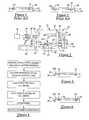
- a substrate 10 having a conductive layer 12 deposited thereonis shown in FIG. 1.
- one or multiple pin holes 14extends through the conductive layer 12 into the wafer 10 for various purposes such as testing or proper alignment of the wafer 10 prior to processing, for example.
- a layer of photoresist 16is deposited on the conductive layer 12 and then is typically subjected to a soft-bake curing step.
- the photoresist 16is subjected to an alignment and exposure step in which the photoresist 16 is exposed to light through a reticle or mask (not shown) to superimpose the circuit pattern in the reticle or mask onto the photoresist 16 by cross-linking the photoresist 16 along the areas of light exposure.
- the underlying conductive layer 12is etched around the etchant-resistant, cross-linked photoresist to form the desired circuit pattern in the conductive layer 12 .
- the photoresist-deposition stepis typically carried out in a coater cup (not shown) which is open to atmospheric pressure in the semiconductor fabrication facility. Accordingly, in the coater cup the photoresist 16 is layered over the conductive layer 12 under atmospheric pressure and extends over the pin holes 14 , as shown in FIG. 1. During this step, air becomes trapped in the pin holes 14 . During the subsequent soft-bake step which is carried out to cure the photoresist 16 , the heated air trapped in the pin holes 14 expands against the overlying photoresist 16 , pushing the photoresist 16 upwardly and forming air bubbles 18 above the respective pin holes 14 , as shown in FIG. 2.
- An object of the present inventionis to provide an apparatus and method for the bubble-free application of a resin to a substrate.
- Another object of the present inventionis to provide an apparatus and method which is suitably adapted for applying a photoresist to a wafer in such a manner as to eliminate the formation of air pockets in the wafer beneath the photoresist.
- Still another object of the present inventionis to provide an apparatus and method which is suitable for preventing the formation of air bubbles in or beneath a layer of photoresist during a soft-bake curing step of photolithography.
- Yet another object of the present inventionis to provide an apparatus and method which may have application to various industries in the bubble-free application of a resin to a substrate.
- a still further object of the present inventionis to provide a method for the bubble-free application of a resin to a substrate, which method includes applying the resin to the substrate under vacuum pressure.
- Yet another object of the present inventionis to provide an apparatus which is suitable for the bubble-free application of a resin to a substrate, which apparatus includes an airtight chamber for receiving the substrate and a resin supply dispenser for dispensing the resin onto the substrate.
- the present inventionis generally directed to an apparatus and method which is suitable for the bubble-free application of a resin to a substrate.
- the apparatustypically includes an airtight chamber which receives the substrate and a resin dispenser for dispensing the liquid resin onto the substrate. After a vacuum pressure is induced in the chamber, the resin is dispensed onto the substrate. Accordingly, air is substantially incapable of becoming trapped between the resin and the substrate and forming air bubbles during subsequent processing of the substrate.
- FIG. 1is a cross-sectional view of a substrate and a photoresist layer dispensed onto the substrate according to a conventional photoresist-dispensing method
- FIG. 2is a cross-sectional view of the substrate of FIG. 1, after the photoresist-coated substrate is subjected to a soft-baking step, more particularly illustrating the formation of air bubbles beneath the photoresist;
- FIG. 3is a side view, partially in cross-section, of an apparatus according to the present invention.
- FIG. 4is a flow diagram illustrating a typical process flow according to the method of the present invention.
- FIG. 5is a cross-sectional view of a substrate and a photoresist layer dispensed onto the substrate in implementation of the apparatus and method of the present invention.
- FIG. 6is a cross-sectional view of the substrate and photoresist layer of FIG. 5, after atmospheric pressure is restored to the apparatus in implementation of the apparatus and method of the present invention.
- the present inventionhas particularly beneficial utility in the bubble-free application of photoresist to a substrate during the course of fabricating IC (integrated circuit) devices on the substrate.
- the inventionis not so limited in application, and while references may be made to such photoresist and integrated circuits, the invention is more generally suitable for the bubble-free application of any type of liquid resin to a substrate in a variety of industrial and mechanical applications.
- an illustrative embodiment of the apparatus 22 in accordance with the present inventionincludes a vacuum chamber 24 , having a chamber wall 26 and a chamber bottom 28 which define a chamber interior 30 .
- a chamber lid 32having a lid flange 33 , removably and sealingly engages the vacuum chamber 24 .
- An o-ring 34 provided on the upper edge of the chamber wall 26 or on the lower surface of the lid flange 33is sandwiched between the upper edge of the chamber wall 26 and the lid flange 33 when the chamber lid 32 is seated on the vacuum chamber 24 , as shown, to provide an airtight seal between the chamber interior 30 and the exterior of the vacuum chamber 24 .
- a substrate spinner 44is provided on the chamber bottom 28 , in the chamber interior 30 .
- the substrate spinner 44contains a spinner motor 45 which rotatably engages the lower end of a shaft 48 that extends upwardly from the spinner 44 .
- a substrate support 46 provided on the upper end of the shaft 48is adapted for holding a substrate 50 , as hereinafter further described.
- a speed controller 66operably engages the spinner motor 45 through a controller shaft 68 which extends through the chamber wall 26 and into the spinner 44 . Accordingly, the spinner motor 45 is operable to rotate the shaft 48 and the substrate support 46 .
- the operational speed of the spinner motor 45is controlled by operation of the speed controller 66 , according to the knowledge of those skilled in the art.
- a vacuum conduit 42is disposed in fluid communication with the chamber interior 30 and may extend through the chamber wall 26 , as shown.
- a vacuum pump 36is provided in fluid communication with the vacuum conduit 42 .
- a bellow 38is provided in the vacuum conduit 42 adjacent to the vacuum pump 36 , and a throttle valve 40 is provided in the vacuum conduit 42 between the bellow 38 and the chamber wall 26 . Accordingly, when the chamber lid 32 sealingly engages the chamber wall 26 , the vacuum pump 36 is operable to partially evacuate air from the chamber interior 30 and through the throttle valve 40 and bellow 38 , respectively, to provide a partial vacuum pressure inside the chamber interior 30 for purposes which will be hereinafter described.
- a photoresist container 56which contains a supply of liquid photoresist 64 , is disposed in fluid communication with the chamber interior 30 through a photoresist delivery conduit 58 , which typically extends through the chamber wall 26 .
- a valve 60is typically provided in the photoresist delivery conduit 58 .
- a photoresist dispensing spout 62disposed above the substrate support 46 inside the chamber interior 30 , is provided in fluid communication with the photoresist delivery conduit 58 .
- the interior of the photoresist container 56may be provided in pneumatic communication with the exterior of the photoresist container 56 to establish atmospheric air pressure inside the photoresist container 56 .
- the liquid photoresist 64is drawn from the photoresist container 56 , through the photoresist delivery conduit 58 and the valve 60 , and is dispensed from the photoresist dispensing spout 62 onto the substrate 50 .
- the valve 60regulates flow of the liquid photoresist 64 from the photoresist container 56 , through the photoresist delivery conduit 58 and photoresist dispensing spout 62 , respectively, and onto the rotating substrate 50 .
- any suitable pumping mechanism(not shown) known by those skilled in the art may be operably connected to the photoresist delivery conduit 58 for measured pumping of the liquid photoresist 64 from the photoresist container 56 and onto the substrate 46 .
- a photoresist layer 64 ais deposited under partial vacuum pressure on a conductive layer 51 previously formed on a substrate 50 .
- Deposit of the photoresist layer 64 a on the substrate 50 under partial-vacuum conditionsprevents the trapping of air in pin holes 52 formed in the substrate 50 and formation of air bubbles (not shown) in the photoresist layer 64 a during the subsequent soft baking step of photolithography. Accordingly, the substrate 50 , having had the conductive layer 51 previously deposited thereon, is initially placed on the substrate support 46 in the chamber interior 30 of the vacuum chamber 24 .
- the vacuum pump 36is operated to draw air from the chamber interior 30 through the vacuum conduit 42 , the throttle valve 40 and the bellow 38 , respectively, until the partial vacuum pressure inside the chamber interior 30 reaches the desired level, typically about 60 torr.
- the valve 60is opened to allow flow of a selected quantity of liquid photoresist 64 from the photoresist container 56 , through the photoresist delivery conduit 58 and onto the conducting layer 51 (FIG. 5) at the center of the substrate 50 , respectively, as atmospheric air pressure in the photoresist container 56 pushes the liquid photoresist 64 from the photoresist container 56 and onto the substrate 50 .
- a selected quantity of liquid photoresist 64from the photoresist container 56 , through the photoresist delivery conduit 58 and onto the conducting layer 51 (FIG. 5) at the center of the substrate 50 , respectively, as atmospheric air pressure in the photoresist container 56 pushes the liquid photoresist 64 from the photoresist container 56 and onto the substrate 50 .
- about 10 ml of the liquid photoresist 64is dispensed onto the center of the substrate 50 .
- the valve 60is closed to prevent further flow of the liquid photoresist 64 from the photoresist container 56 and onto the substrate 50
- the substrate support 46 and substrate 50are next rotated by operation of the spinner motor 45 , initially at a typical speed of about 300 rpm. Accordingly, centrifugal force imparted by the rotating substrate 50 pulls the liquid photoresist 64 from the center toward the edge of the substrate 50 to provide a substantially uniform spread of the liquid photoresist 64 on the conductive layer 51 .
- the speed controller 66By operation of the speed controller 66 , the rotational speed of the substrate support 46 is gradually increased to about 550 rpm in order to obtain a final thickness of the photoresist layer 64 a of typically about 30 Am. At that point, rotation of the substrate support 46 is terminated and the photoresist layer 64 a extends over the pin holes 52 in the substrate 50 , as shown in FIG. 5.
- atmospheric pressure in the chamber interior 30is re-established by releasing vacuum pressure induced therein by the vacuum pump 36 . Because the air pressure in each of the pin holes 52 equals the partial vacuum pressure induced in the chamber interior 30 during application of the photoresist layer 64 a , the re-established atmospheric pressure in the chamber interior 30 pushes the hole-spanning segments of the pliant photoresist layer 64 a into the respective pin holes 52 , causing depressions 54 at the respective pin holes 52 , as shown in FIG. 6.
- the substrate 50is removed from the chamber interior 30 and subjected to a soft bake process at a downstream processing tool (not shown) to cure the photoresist layer 64 a , after which the substrate 50 is subjected to an alignment and exposure step in which a circuit pattern is superimposed on the photoresist layer 64 a through a mask or reticle (not shown). Accordingly, air bubbles which otherwise would have formed in the photoresist layer 64 a at the pin holes 52 during the soft bake curing step are not present to interfere with the alignment and exposure step prior to etching of the circuit pattern in the underlying conductive layer 51 .
- the substrate 50is typically subjected to a plasma ashing and wet stripping process, in conventional fashion, to remove the residual photoresist 64 a from the substrate 50 , leaving the circuit pattern in the conductive layer 51 .
Landscapes
- Engineering & Computer Science (AREA)
- Physics & Mathematics (AREA)
- Condensed Matter Physics & Semiconductors (AREA)
- General Physics & Mathematics (AREA)
- Manufacturing & Machinery (AREA)
- Computer Hardware Design (AREA)
- Microelectronics & Electronic Packaging (AREA)
- Power Engineering (AREA)
- Application Of Or Painting With Fluid Materials (AREA)
Abstract
Description
- The present invention relates to photolithography processes used in the formation of integrated circuit (IC) patterns on photoresist in the fabrication of semiconductor integrated circuits. More particularly, the present invention relates to an apparatus and method for application of a resin such as a photoresist onto a substrate under vacuum pressure to prevent the formation of bubbles on the substrate during subsequent substrate processing under elevated temperatures.[0001]
- The fabrication of various solid state devices requires the use of planar substrates, or semiconductor wafers, on which integrated circuits are fabricated. The final number, or yield, of functional integrated circuits on a wafer at the end of the IC fabrication process is of utmost importance to semiconductor manufacturers, and increasing the yield of circuits on the wafer is the main goal of semiconductor fabrication. After packaging, the circuits on the wafers are tested, wherein non-functional dies are marked using an inking process and the functional dies on the wafer are separated and sold. IC fabricators increase the yield of dies on a wafer by exploiting economies of scale. Over 1000 dies may be formed on a single wafer which measures from six to twelve inches in diameter.[0002]
- Various processing steps are used to fabricate integrated circuits on a semiconductor wafer. These steps include spin-coating of a conducting layer on the silicon wafer substrate; formation of a photoresist or other mask such as titanium oxide or silicon oxide, in the form of the desired metal interconnection pattern, using standard lithographic or photolithographic techniques; subjecting the wafer substrate to a dry etching process to remove the conducting layer from the areas not covered by the mask, thereby etching the conducting layer in the form of the masked pattern on the substrate; removing or stripping the mask layer from the substrate typically using reactive plasma and chlorine gas, thereby exposing the top surface of the conductive interconnect layer; and cooling and drying the wafer substrate by applying water and nitrogen gas to the wafer substrate.[0003]
- Spin coating of photoresist on wafers, as well as the other steps in the photolithography process, is carried out in an automated coater/developer track system using wafer handling equipment which transport the wafers between the various photolithography operation stations, such as vapor prime resist spin coat, develop, baking and chilling stations. Robotic handling of the wafers minimizes particle generation and wafer damage. Automated wafer tracks enable various processing operations to be carried out simultaneously. Two types of automated track systems widely used in the industry are the TEL (Tokyo Electron Limited) track and the SVG (Silicon Valley Group) track.[0004]
- Photoresist materials are coated onto the surface of a wafer by dispensing a photoresist fluid typically on the center of the wafer as the wafer rotates at high speeds within a stationary bowl or coater cup. The coater cup catches excess fluids and particles ejected from the rotating wafer during application of the photoresist. The photoresist fluid dispensed onto the center of the wafer is spread outwardly toward the edges of the wafer by surface tension generated by the centrifugal force of the rotating wafer. This facilitates uniform application of the liquid photoresist on the entire surface of the wafer.[0005]
- After it is layered on the substrate, the photoresist is exposed to light through a mask or reticle in an alignment and exposure process. A reticle is a transparent plate patterned with a circuit image to be formed in the photoresist coating on the wafer. A reticle contains the circuit pattern image for only a few of the die on a wafer, such as four die, for example, and thus, must be stepped and repeated across the entire surface of the wafer. In contrast, a photomask, or mask, includes the circuit pattern image for all of the die on a wafer and requires only one exposure to transfer the circuit pattern image for all of the dies to the wafer. After alignment and exposure, the photoresist is developed.[0006]
- The circuit pattern defined by the developed and hardened photoresist is next transferred to the underlying metal conductive layer using a metal etching process, in which metal over the entire surface of the wafer and not covered by the cross-linked photoresist is etched away from the wafer with the metal under the cross-linked photoresist that defines the circuit pattern protected from the etchant. As a result, a well-defined pattern of metallic microelectronic circuits which closely approximates the cross-linked photoresist circuit pattern remains in the metal layer.[0007]
- The numerous processing steps outlined above are used to cumulatively apply multiple electrically conductive and insulative layers on the wafer and pattern the layers to form the circuits. The final yield of functional circuits on the wafer depends on proper application of each layer during the process steps. Proper application of those layers depends, in turn, on coating the material in a uniform spread over the surface of the wafer in an economical and efficient manner.[0008]
- A typical method of forming a circuit pattern on a wafer includes introducing the wafer into the automated track system and then spin-coating a photoresist layer onto the wafer. The photoresist is next cured by conducting a soft bake process. After it is cooled, the wafer is placed in an exposure apparatus, such as a stepper, which aligns the wafer with an array of die patterns etched on the typically chrome-coated quartz reticle. When properly aligned and focused, the stepper exposes a small area of the wafer, then shifts or “steps” to the next field and repeats the process until the entire wafer surface has been exposed to the die patterns on the reticle. The photoresist is exposed to light through the reticle in the circuit image pattern. Exposure of the photoresist to this image pattern cross-links and hardens the resist in the circuit pattern. After the aligning and exposing step, the wafer is exposed to post-exposure baking and then is developed and hard-baked to develop the photoresist pattern.[0009]
- A[0010]
substrate 10 having aconductive layer 12 deposited thereon is shown in FIG. 1. Frequently, one ormultiple pin holes 14 extends through theconductive layer 12 into thewafer 10 for various purposes such as testing or proper alignment of thewafer 10 prior to processing, for example. A layer ofphotoresist 16 is deposited on theconductive layer 12 and then is typically subjected to a soft-bake curing step. Next, thephotoresist 16 is subjected to an alignment and exposure step in which thephotoresist 16 is exposed to light through a reticle or mask (not shown) to superimpose the circuit pattern in the reticle or mask onto thephotoresist 16 by cross-linking thephotoresist 16 along the areas of light exposure. Finally, the underlyingconductive layer 12 is etched around the etchant-resistant, cross-linked photoresist to form the desired circuit pattern in theconductive layer 12. - The photoresist-deposition step is typically carried out in a coater cup (not shown) which is open to atmospheric pressure in the semiconductor fabrication facility. Accordingly, in the coater cup the[0011]
photoresist 16 is layered over theconductive layer 12 under atmospheric pressure and extends over thepin holes 14, as shown in FIG. 1. During this step, air becomes trapped in thepin holes 14. During the subsequent soft-bake step which is carried out to cure thephotoresist 16, the heated air trapped in thepin holes 14 expands against the overlyingphotoresist 16, pushing thephotoresist 16 upwardly and formingair bubbles 18 above therespective pin holes 14, as shown in FIG. 2. Theseair bubbles 18 interfere with subsequent processing of thesubstrate 10, particularly the alignment and exposure process which is carried out after the soft bake curing step to superimpose the circuit pattern image from the mask or reticle onto thephotoresist 16. Accordingly, an apparatus and method is needed for carrying out the photoresist-coating step in such a manner as to eliminate the formation of air bubbles in the photoresist during the soft bake photoresist-curing step. - An object of the present invention is to provide an apparatus and method for the bubble-free application of a resin to a substrate.[0012]
- Another object of the present invention is to provide an apparatus and method which is suitably adapted for applying a photoresist to a wafer in such a manner as to eliminate the formation of air pockets in the wafer beneath the photoresist.[0013]
- Still another object of the present invention is to provide an apparatus and method which is suitable for preventing the formation of air bubbles in or beneath a layer of photoresist during a soft-bake curing step of photolithography.[0014]
- Yet another object of the present invention is to provide an apparatus and method which may have application to various industries in the bubble-free application of a resin to a substrate.[0015]
- A still further object of the present invention is to provide a method for the bubble-free application of a resin to a substrate, which method includes applying the resin to the substrate under vacuum pressure.[0016]
- Yet another object of the present invention is to provide an apparatus which is suitable for the bubble-free application of a resin to a substrate, which apparatus includes an airtight chamber for receiving the substrate and a resin supply dispenser for dispensing the resin onto the substrate.[0017]
- In accordance with these and other objects and advantages, the present invention is generally directed to an apparatus and method which is suitable for the bubble-free application of a resin to a substrate. The apparatus typically includes an airtight chamber which receives the substrate and a resin dispenser for dispensing the liquid resin onto the substrate. After a vacuum pressure is induced in the chamber, the resin is dispensed onto the substrate. Accordingly, air is substantially incapable of becoming trapped between the resin and the substrate and forming air bubbles during subsequent processing of the substrate.[0018]
- The invention will now be described, by way of example, with reference to the accompanying drawing, in which:[0019]
- FIG. 1 is a cross-sectional view of a substrate and a photoresist layer dispensed onto the substrate according to a conventional photoresist-dispensing method;[0020]
- FIG. 2 is a cross-sectional view of the substrate of FIG. 1, after the photoresist-coated substrate is subjected to a soft-baking step, more particularly illustrating the formation of air bubbles beneath the photoresist;[0021]
- FIG. 3 is a side view, partially in cross-section, of an apparatus according to the present invention;[0022]
- FIG. 4 is a flow diagram illustrating a typical process flow according to the method of the present invention;[0023]
- FIG. 5 is a cross-sectional view of a substrate and a photoresist layer dispensed onto the substrate in implementation of the apparatus and method of the present invention; and[0024]
- FIG. 6 is a cross-sectional view of the substrate and photoresist layer of FIG. 5, after atmospheric pressure is restored to the apparatus in implementation of the apparatus and method of the present invention.[0025]
- The present invention has particularly beneficial utility in the bubble-free application of photoresist to a substrate during the course of fabricating IC (integrated circuit) devices on the substrate. However, the invention is not so limited in application, and while references may be made to such photoresist and integrated circuits, the invention is more generally suitable for the bubble-free application of any type of liquid resin to a substrate in a variety of industrial and mechanical applications.[0026]
- Referring initially to FIG. 3, an illustrative embodiment of the[0027]
apparatus 22 in accordance with the present invention includes avacuum chamber 24, having achamber wall 26 and a chamber bottom28 which define achamber interior 30. Achamber lid 32, having alid flange 33, removably and sealingly engages thevacuum chamber 24. An o-ring 34 provided on the upper edge of thechamber wall 26 or on the lower surface of thelid flange 33 is sandwiched between the upper edge of thechamber wall 26 and thelid flange 33 when thechamber lid 32 is seated on thevacuum chamber 24, as shown, to provide an airtight seal between thechamber interior 30 and the exterior of thevacuum chamber 24. Asubstrate spinner 44 is provided on the chamber bottom28, in thechamber interior 30. Thesubstrate spinner 44 contains aspinner motor 45 which rotatably engages the lower end of ashaft 48 that extends upwardly from thespinner 44. Asubstrate support 46 provided on the upper end of theshaft 48 is adapted for holding asubstrate 50, as hereinafter further described. Aspeed controller 66 operably engages thespinner motor 45 through acontroller shaft 68 which extends through thechamber wall 26 and into thespinner 44. Accordingly, thespinner motor 45 is operable to rotate theshaft 48 and thesubstrate support 46. The operational speed of thespinner motor 45 is controlled by operation of thespeed controller 66, according to the knowledge of those skilled in the art. - A[0028]
vacuum conduit 42 is disposed in fluid communication with thechamber interior 30 and may extend through thechamber wall 26, as shown. Avacuum pump 36 is provided in fluid communication with thevacuum conduit 42. Abellow 38 is provided in thevacuum conduit 42 adjacent to thevacuum pump 36, and athrottle valve 40 is provided in thevacuum conduit 42 between thebellow 38 and thechamber wall 26. Accordingly, when thechamber lid 32 sealingly engages thechamber wall 26, thevacuum pump 36 is operable to partially evacuate air from thechamber interior 30 and through thethrottle valve 40 andbellow 38, respectively, to provide a partial vacuum pressure inside thechamber interior 30 for purposes which will be hereinafter described. - A[0029]
photoresist container 56, which contains a supply ofliquid photoresist 64, is disposed in fluid communication with thechamber interior 30 through aphotoresist delivery conduit 58, which typically extends through thechamber wall 26. Avalve 60 is typically provided in thephotoresist delivery conduit 58. Aphotoresist dispensing spout 62, disposed above thesubstrate support 46 inside thechamber interior 30, is provided in fluid communication with thephotoresist delivery conduit 58. The interior of thephotoresist container 56 may be provided in pneumatic communication with the exterior of thephotoresist container 56 to establish atmospheric air pressure inside thephotoresist container 56. Accordingly, responsive to vacuum pressure induced in thechamber interior 30 by operation of thevacuum pump 36, as hereinafter described, theliquid photoresist 64 is drawn from thephotoresist container 56, through thephotoresist delivery conduit 58 and thevalve 60, and is dispensed from thephotoresist dispensing spout 62 onto thesubstrate 50. Thevalve 60 regulates flow of theliquid photoresist 64 from thephotoresist container 56, through thephotoresist delivery conduit 58 andphotoresist dispensing spout 62, respectively, and onto the rotatingsubstrate 50. Alternatively, it is understood that any suitable pumping mechanism (not shown) known by those skilled in the art may be operably connected to thephotoresist delivery conduit 58 for measured pumping of theliquid photoresist 64 from thephotoresist container 56 and onto thesubstrate 46. - Referring next to FIGS.[0030]3-6, in typical operation of the
apparatus 22 according to the method of the present invention, aphotoresist layer 64ais deposited under partial vacuum pressure on aconductive layer 51 previously formed on asubstrate 50. Deposit of thephotoresist layer 64aon thesubstrate 50 under partial-vacuum conditions prevents the trapping of air in pin holes52 formed in thesubstrate 50 and formation of air bubbles (not shown) in thephotoresist layer 64aduring the subsequent soft baking step of photolithography. Accordingly, thesubstrate 50, having had theconductive layer 51 previously deposited thereon, is initially placed on thesubstrate support 46 in thechamber interior 30 of thevacuum chamber 24. After thechamber lid 32 is placed on thevacuum chamber 24 to provide an airtight seal between thechamber interior 30 and the outside of thevacuum chamber 24, thevacuum pump 36 is operated to draw air from thechamber interior 30 through thevacuum conduit 42, thethrottle valve 40 and thebellow 38, respectively, until the partial vacuum pressure inside thechamber interior 30 reaches the desired level, typically about 60 torr. - Next, the[0031]
valve 60 is opened to allow flow of a selected quantity ofliquid photoresist 64 from thephotoresist container 56, through thephotoresist delivery conduit 58 and onto the conducting layer51 (FIG. 5) at the center of thesubstrate 50, respectively, as atmospheric air pressure in thephotoresist container 56 pushes theliquid photoresist 64 from thephotoresist container 56 and onto thesubstrate 50. Typically, about 10 ml of theliquid photoresist 64 is dispensed onto the center of thesubstrate 50. However, it is understood that the quantity ofliquid photoresist 64 dispensed onto thesubstrate 50 may vary depending on the application. After the desired quantity ofliquid photoresist 64 is dispensed onto thesubstrate 50, thevalve 60 is closed to prevent further flow of theliquid photoresist 64 from thephotoresist container 56 and onto thesubstrate 50. - The[0032]
substrate support 46 andsubstrate 50 are next rotated by operation of thespinner motor 45, initially at a typical speed of about 300 rpm. Accordingly, centrifugal force imparted by the rotatingsubstrate 50 pulls theliquid photoresist 64 from the center toward the edge of thesubstrate 50 to provide a substantially uniform spread of theliquid photoresist 64 on theconductive layer 51. By operation of thespeed controller 66, the rotational speed of thesubstrate support 46 is gradually increased to about 550 rpm in order to obtain a final thickness of thephotoresist layer 64aof typically about30 Am. At that point, rotation of thesubstrate support 46 is terminated and thephotoresist layer 64aextends over the pin holes52 in thesubstrate 50, as shown in FIG. 5. - Finally, atmospheric pressure in the[0033]
chamber interior 30 is re-established by releasing vacuum pressure induced therein by thevacuum pump 36. Because the air pressure in each of the pin holes52 equals the partial vacuum pressure induced in thechamber interior 30 during application of thephotoresist layer 64a, the re-established atmospheric pressure in thechamber interior 30 pushes the hole-spanning segments of thepliant photoresist layer 64ainto the respective pin holes52, causingdepressions 54 at the respective pin holes52, as shown in FIG. 6. Next, thesubstrate 50 is removed from thechamber interior 30 and subjected to a soft bake process at a downstream processing tool (not shown) to cure thephotoresist layer 64a, after which thesubstrate 50 is subjected to an alignment and exposure step in which a circuit pattern is superimposed on thephotoresist layer 64athrough a mask or reticle (not shown). Accordingly, air bubbles which otherwise would have formed in thephotoresist layer 64aat the pin holes52 during the soft bake curing step are not present to interfere with the alignment and exposure step prior to etching of the circuit pattern in the underlyingconductive layer 51. After the metal etching process, thesubstrate 50 is typically subjected to a plasma ashing and wet stripping process, in conventional fashion, to remove theresidual photoresist 64afrom thesubstrate 50, leaving the circuit pattern in theconductive layer 51. - While the preferred embodiments of the invention have been described above, it will be recognized and understood that various modifications can be made in the invention and the appended claims are intended to cover all such modifications which may fall within the spirit and scope of the invention.[0034]
Claims (20)
Priority Applications (1)
| Application Number | Priority Date | Filing Date | Title |
|---|---|---|---|
| US10/341,993US6846360B2 (en) | 2003-01-13 | 2003-01-13 | Apparatus and method for bubble-free application of a resin to a substrate |
Applications Claiming Priority (1)
| Application Number | Priority Date | Filing Date | Title |
|---|---|---|---|
| US10/341,993US6846360B2 (en) | 2003-01-13 | 2003-01-13 | Apparatus and method for bubble-free application of a resin to a substrate |
Publications (2)
| Publication Number | Publication Date |
|---|---|
| US20040134420A1true US20040134420A1 (en) | 2004-07-15 |
| US6846360B2 US6846360B2 (en) | 2005-01-25 |
Family
ID=32711629
Family Applications (1)
| Application Number | Title | Priority Date | Filing Date |
|---|---|---|---|
| US10/341,993Expired - Fee RelatedUS6846360B2 (en) | 2003-01-13 | 2003-01-13 | Apparatus and method for bubble-free application of a resin to a substrate |
Country Status (1)
| Country | Link |
|---|---|
| US (1) | US6846360B2 (en) |
Cited By (14)
| Publication number | Priority date | Publication date | Assignee | Title |
|---|---|---|---|---|
| US20040147066A1 (en)* | 2003-01-17 | 2004-07-29 | Semiconductor Energy Laboratory Co., Ltd. | Method for manufacturing resist pattern and method for manufacturing semiconductor device |
| US20050028314A1 (en)* | 2003-08-06 | 2005-02-10 | Hickman Craig A. | Photolithographic stepper and/or scanner machines including cleaning devices and methods of cleaning photolithographic stepper and/or scanner machines |
| US20050231704A1 (en)* | 2004-04-14 | 2005-10-20 | Asml Netherlands B.V. | Device manufacturing method |
| US20060049151A1 (en)* | 2004-09-03 | 2006-03-09 | Lee Yong H | Plasma display apparatus including electrode pad |
| WO2007027311A3 (en)* | 2005-08-29 | 2007-07-19 | Micron Technology Inc | Systems and methods for controlling ambient pressure during processing of microfeature workpieces, including during immersion lithography |
| US20070165199A1 (en)* | 2006-01-18 | 2007-07-19 | Micron Technology, Inc. | Immersion photolithography scanner |
| US20080087217A1 (en)* | 2003-05-01 | 2008-04-17 | Seiko Epson Corporation | Coating apparatus, thin film forming method, thin film forming apparatus, and semiconductor device manufacturing method, electro-optic device and electronic instrument |
| US20090129897A1 (en)* | 2007-05-09 | 2009-05-21 | Brooks Automation, Inc. | Side opening unified pod |
| US20120225560A1 (en)* | 2011-03-04 | 2012-09-06 | Stmicroelectronics (Crolles 2) Sas | Manufacturing method of integrated circuits based on formation of lines and trenches |
| TWI476824B (en)* | 2008-06-18 | 2015-03-11 | Taiwan Semiconductor Mfg Co Ltd | Method for removing bubble in resin, and method of manufacturing diamond disk |
| US20160217997A1 (en)* | 2015-01-23 | 2016-07-28 | Kabushiki Kaisha Toshiba | Substrate processing device, recordng medium, and control method |
| TWI547772B (en)* | 2014-10-01 | 2016-09-01 | 力晶科技股份有限公司 | Photoresist recycle system and method thereof |
| CN111957529A (en)* | 2020-08-16 | 2020-11-20 | 南通新江海动力电子有限公司 | Lifting type vacuum glue pouring equipment |
| WO2021110957A1 (en)* | 2019-12-04 | 2021-06-10 | Metalizz | Method for treating the surface of a three-dimensional object |
Families Citing this family (4)
| Publication number | Priority date | Publication date | Assignee | Title |
|---|---|---|---|---|
| US7563835B2 (en)* | 2001-12-28 | 2009-07-21 | Sun Chemical Corporation | Solventless universal colorants |
| JP4828828B2 (en)* | 2003-02-28 | 2011-11-30 | 富士通株式会社 | Etching resistant film and method for manufacturing the same, surface-cured resist pattern and method for manufacturing the same, and semiconductor device and method for manufacturing the same |
| US20070228593A1 (en)* | 2006-04-03 | 2007-10-04 | Molecular Imprints, Inc. | Residual Layer Thickness Measurement and Correction |
| JP6445974B2 (en) | 2013-10-05 | 2019-01-09 | 武蔵エンジニアリング株式会社 | Liquid material filling apparatus and method |
Citations (3)
| Publication number | Priority date | Publication date | Assignee | Title |
|---|---|---|---|---|
| US4990208A (en)* | 1986-10-31 | 1991-02-05 | Seiko Epson Corporation, A Japanese Corporation | Method of manufacturing an optical recording medium |
| US6063190A (en)* | 1993-03-25 | 2000-05-16 | Tokyo Electron Limited | Method of forming coating film and apparatus therefor |
| US6627038B2 (en)* | 2000-05-09 | 2003-09-30 | Canon Kabushiki Kaisha | Processing chamber |
- 2003
- 2003-01-13USUS10/341,993patent/US6846360B2/ennot_activeExpired - Fee Related
Patent Citations (3)
| Publication number | Priority date | Publication date | Assignee | Title |
|---|---|---|---|---|
| US4990208A (en)* | 1986-10-31 | 1991-02-05 | Seiko Epson Corporation, A Japanese Corporation | Method of manufacturing an optical recording medium |
| US6063190A (en)* | 1993-03-25 | 2000-05-16 | Tokyo Electron Limited | Method of forming coating film and apparatus therefor |
| US6627038B2 (en)* | 2000-05-09 | 2003-09-30 | Canon Kabushiki Kaisha | Processing chamber |
Cited By (26)
| Publication number | Priority date | Publication date | Assignee | Title |
|---|---|---|---|---|
| US20040147066A1 (en)* | 2003-01-17 | 2004-07-29 | Semiconductor Energy Laboratory Co., Ltd. | Method for manufacturing resist pattern and method for manufacturing semiconductor device |
| US7405033B2 (en)* | 2003-01-17 | 2008-07-29 | Semiconductor Energy Laboratory Co., Ltd. | Method for manufacturing resist pattern and method for manufacturing semiconductor device |
| US20080087217A1 (en)* | 2003-05-01 | 2008-04-17 | Seiko Epson Corporation | Coating apparatus, thin film forming method, thin film forming apparatus, and semiconductor device manufacturing method, electro-optic device and electronic instrument |
| US20050028314A1 (en)* | 2003-08-06 | 2005-02-10 | Hickman Craig A. | Photolithographic stepper and/or scanner machines including cleaning devices and methods of cleaning photolithographic stepper and/or scanner machines |
| US20060201540A1 (en)* | 2003-08-06 | 2006-09-14 | Micron Technology, Inc. | Photolithographic stepper and/or scanner machines including cleaning devices and methods of cleaning photolithographic stepper and/or scanner machines |
| US7361234B2 (en) | 2003-08-06 | 2008-04-22 | Micron Technology, Inc. | Photolithographic stepper and/or scanner machines including cleaning devices and methods of cleaning photolithographic stepper and/or scanner machines |
| US7370659B2 (en) | 2003-08-06 | 2008-05-13 | Micron Technology, Inc. | Photolithographic stepper and/or scanner machines including cleaning devices and methods of cleaning photolithographic stepper and/or scanner machines |
| US7463336B2 (en)* | 2004-04-14 | 2008-12-09 | Asml Netherlands B.V. | Device manufacturing method and apparatus with applied electric field |
| US20050231704A1 (en)* | 2004-04-14 | 2005-10-20 | Asml Netherlands B.V. | Device manufacturing method |
| US20060049151A1 (en)* | 2004-09-03 | 2006-03-09 | Lee Yong H | Plasma display apparatus including electrode pad |
| WO2007027311A3 (en)* | 2005-08-29 | 2007-07-19 | Micron Technology Inc | Systems and methods for controlling ambient pressure during processing of microfeature workpieces, including during immersion lithography |
| US7456928B2 (en) | 2005-08-29 | 2008-11-25 | Micron Technology, Inc. | Systems and methods for controlling ambient pressure during processing of microfeature workpieces, including during immersion lithography |
| US20070165199A1 (en)* | 2006-01-18 | 2007-07-19 | Micron Technology, Inc. | Immersion photolithography scanner |
| US8472004B2 (en) | 2006-01-18 | 2013-06-25 | Micron Technology, Inc. | Immersion photolithography scanner |
| US9105673B2 (en)* | 2007-05-09 | 2015-08-11 | Brooks Automation, Inc. | Side opening unified pod |
| US20090129897A1 (en)* | 2007-05-09 | 2009-05-21 | Brooks Automation, Inc. | Side opening unified pod |
| US9978623B2 (en) | 2007-05-09 | 2018-05-22 | Brooks Automation, Inc. | Side opening unified pod |
| US20180269094A1 (en)* | 2007-05-17 | 2018-09-20 | Brooks Automation, Inc. | Side opening unified pod |
| US11201070B2 (en) | 2007-05-17 | 2021-12-14 | Brooks Automation, Inc. | Side opening unified pod |
| TWI476824B (en)* | 2008-06-18 | 2015-03-11 | Taiwan Semiconductor Mfg Co Ltd | Method for removing bubble in resin, and method of manufacturing diamond disk |
| US20120225560A1 (en)* | 2011-03-04 | 2012-09-06 | Stmicroelectronics (Crolles 2) Sas | Manufacturing method of integrated circuits based on formation of lines and trenches |
| TWI547772B (en)* | 2014-10-01 | 2016-09-01 | 力晶科技股份有限公司 | Photoresist recycle system and method thereof |
| US20160217997A1 (en)* | 2015-01-23 | 2016-07-28 | Kabushiki Kaisha Toshiba | Substrate processing device, recordng medium, and control method |
| WO2021110957A1 (en)* | 2019-12-04 | 2021-06-10 | Metalizz | Method for treating the surface of a three-dimensional object |
| FR3104038A1 (en)* | 2019-12-04 | 2021-06-11 | Metalizz | A method of treating the surface of a three-dimensional object |
| CN111957529A (en)* | 2020-08-16 | 2020-11-20 | 南通新江海动力电子有限公司 | Lifting type vacuum glue pouring equipment |
Also Published As
| Publication number | Publication date |
|---|---|
| US6846360B2 (en) | 2005-01-25 |
Similar Documents
| Publication | Publication Date | Title |
|---|---|---|
| US6846360B2 (en) | Apparatus and method for bubble-free application of a resin to a substrate | |
| US7224427B2 (en) | Megasonic immersion lithography exposure apparatus and method | |
| US20040216770A1 (en) | Process for rinsing and drying substrates | |
| US6548110B1 (en) | Process liquid dispense method and apparatus | |
| US20030101929A1 (en) | Substrate processing apparatus | |
| US6179922B1 (en) | CVD photo resist deposition | |
| US6506688B2 (en) | Method for removing photoresist layer on wafer edge | |
| US6492284B2 (en) | Reactor for processing a workpiece using sonic energy | |
| US7683291B2 (en) | Substrate processing method and manufacturing method of semiconductor device | |
| US20040115957A1 (en) | Apparatus and method for enhancing wet stripping of photoresist | |
| US6248169B1 (en) | Dual-cup coating apparatus | |
| US6232247B1 (en) | Substrate coating apparatus and semiconductor processing method of improving uniformity of liquid deposition | |
| US7029801B2 (en) | Method of manufacturing mask for electron beam lithography and mask blank for electron beam lithography | |
| US6736896B2 (en) | Gas spray arm for spin coating apparatus | |
| US7390753B2 (en) | In-situ plasma treatment of advanced resists in fine pattern definition | |
| US6907742B2 (en) | Apparatus and method for controlling wafer temperature | |
| US7044662B2 (en) | Developing photoresist with supercritical fluid and developer | |
| US20050192699A1 (en) | Temperature-sensing wafer position detection system and method | |
| US20040188547A1 (en) | Developer dispensing nozzle with movable shutter plates | |
| US6765645B1 (en) | De-pellicle tool | |
| US20050051196A1 (en) | Developer dispensing apparatus with adjustable knife ring | |
| US6780461B2 (en) | Environment exchange control for material on a wafer surface | |
| US7368229B2 (en) | Composite layer method for minimizing PED effect | |
| US20040149322A1 (en) | Automatically-adjusting substrate rinsing system | |
| US20090023297A1 (en) | Method and apparatus for hmds treatment of substrate edges |
Legal Events
| Date | Code | Title | Description |
|---|---|---|---|
| AS | Assignment | Owner name:APTOS CORPORATION, CALIFORNIA Free format text:ASSIGNMENT OF ASSIGNORS INTEREST;ASSIGNOR:LEI, KUO-LUNG;REEL/FRAME:013664/0949 Effective date:20021030 | |
| AS | Assignment | Owner name:SURE TALENT INVESTMENT LIMITED, VIRGIN ISLANDS, BR Free format text:ASSIGNMENT OF ASSIGNORS INTEREST;ASSIGNOR:APTOS CORPORATION;REEL/FRAME:017145/0787 Effective date:20050518 | |
| FPAY | Fee payment | Year of fee payment:4 | |
| AS | Assignment | Owner name:HON HAI PRECISION INDUSTRY CO., LTD, TAIWAN Free format text:ASSIGNMENT OF ASSIGNORS INTEREST;ASSIGNOR:SURE TALENT INVESTMENT LIMITED;REEL/FRAME:022288/0984 Effective date:20090220 | |
| FEPP | Fee payment procedure | Free format text:PAT HOLDER NO LONGER CLAIMS SMALL ENTITY STATUS, ENTITY STATUS SET TO UNDISCOUNTED (ORIGINAL EVENT CODE: STOL); ENTITY STATUS OF PATENT OWNER: LARGE ENTITY Free format text:PAYOR NUMBER ASSIGNED (ORIGINAL EVENT CODE: ASPN); ENTITY STATUS OF PATENT OWNER: LARGE ENTITY | |
| FPAY | Fee payment | Year of fee payment:8 | |
| REMI | Maintenance fee reminder mailed | ||
| LAPS | Lapse for failure to pay maintenance fees | ||
| STCH | Information on status: patent discontinuation | Free format text:PATENT EXPIRED DUE TO NONPAYMENT OF MAINTENANCE FEES UNDER 37 CFR 1.362 | |
| FP | Lapsed due to failure to pay maintenance fee | Effective date:20170125 |