US20040126975A1 - Double gate semiconductor device having separate gates - Google Patents
Double gate semiconductor device having separate gatesDownload PDFInfo
- Publication number
- US20040126975A1 US20040126975A1US10/602,061US60206103AUS2004126975A1US 20040126975 A1US20040126975 A1US 20040126975A1US 60206103 AUS60206103 AUS 60206103AUS 2004126975 A1US2004126975 A1US 2004126975A1
- Authority
- US
- United States
- Prior art keywords
- gate
- fin
- semiconductor device
- insulating layer
- gate electrode
- Prior art date
- Legal status (The legal status is an assumption and is not a legal conclusion. Google has not performed a legal analysis and makes no representation as to the accuracy of the status listed.)
- Abandoned
Links
- 239000004065semiconductorSubstances0.000titleclaimsabstractdescription46
- 239000000758substrateSubstances0.000claimsabstractdescription15
- 239000000463materialSubstances0.000claimsdescription32
- 238000000034methodMethods0.000claimsdescription18
- 229910052710siliconInorganic materials0.000claimsdescription18
- 239000010703siliconSubstances0.000claimsdescription18
- 229910052732germaniumInorganic materials0.000claimsdescription8
- GNPVGFCGXDBREM-UHFFFAOYSA-Ngermanium atomChemical compound[Ge]GNPVGFCGXDBREM-UHFFFAOYSA-N0.000claimsdescription8
- 238000004519manufacturing processMethods0.000claimsdescription7
- 238000005530etchingMethods0.000claimsdescription5
- 238000000151depositionMethods0.000claimsdescription3
- 238000000137annealingMethods0.000claimsdescription2
- 239000012535impuritySubstances0.000claimsdescription2
- 238000005498polishingMethods0.000claimsdescription2
- ATJFFYVFTNAWJD-UHFFFAOYSA-NTinChemical compound[Sn]ATJFFYVFTNAWJD-UHFFFAOYSA-N0.000claims1
- 150000004767nitridesChemical class0.000claims1
- XUIMIQQOPSSXEZ-UHFFFAOYSA-NSiliconChemical compound[Si]XUIMIQQOPSSXEZ-UHFFFAOYSA-N0.000description28
- VYPSYNLAJGMNEJ-UHFFFAOYSA-NSilicium dioxideChemical compoundO=[Si]=OVYPSYNLAJGMNEJ-UHFFFAOYSA-N0.000description6
- 230000015572biosynthetic processEffects0.000description6
- 230000008569processEffects0.000description6
- 229910021420polycrystalline siliconInorganic materials0.000description5
- 238000005229chemical vapour depositionMethods0.000description4
- 229920002120photoresistant polymerPolymers0.000description4
- 229920005591polysiliconPolymers0.000description4
- 229910052751metalInorganic materials0.000description3
- 239000002184metalSubstances0.000description3
- 229910052681coesiteInorganic materials0.000description2
- 229910052906cristobaliteInorganic materials0.000description2
- 230000000694effectsEffects0.000description2
- 238000002513implantationMethods0.000description2
- 230000006698inductionEffects0.000description2
- 238000004518low pressure chemical vapour depositionMethods0.000description2
- 238000012986modificationMethods0.000description2
- 230000004048modificationEffects0.000description2
- 239000000377silicon dioxideSubstances0.000description2
- 229910052814silicon oxideInorganic materials0.000description2
- 229910052682stishoviteInorganic materials0.000description2
- 229910052905tridymiteInorganic materials0.000description2
- 208000031481Pathologic ConstrictionDiseases0.000description1
- 229910052581Si3N4Inorganic materials0.000description1
- 229910000577Silicon-germaniumInorganic materials0.000description1
- LEVVHYCKPQWKOP-UHFFFAOYSA-N[Si].[Ge]Chemical compound[Si].[Ge]LEVVHYCKPQWKOP-UHFFFAOYSA-N0.000description1
- 230000004913activationEffects0.000description1
- 230000003667anti-reflective effectEffects0.000description1
- 230000015556catabolic processEffects0.000description1
- 238000006731degradation reactionMethods0.000description1
- 239000003989dielectric materialSubstances0.000description1
- 239000002019doping agentSubstances0.000description1
- 230000005684electric fieldEffects0.000description1
- 238000010292electrical insulationMethods0.000description1
- 230000005669field effectEffects0.000description1
- 239000012212insulatorSubstances0.000description1
- 230000010354integrationEffects0.000description1
- 238000005468ion implantationMethods0.000description1
- 150000002500ionsChemical class0.000description1
- 238000001459lithographyMethods0.000description1
- 229910044991metal oxideInorganic materials0.000description1
- 150000004706metal oxidesChemical class0.000description1
- 238000001465metallisationMethods0.000description1
- 150000002739metalsChemical class0.000description1
- 229910021421monocrystalline siliconInorganic materials0.000description1
- 230000000149penetrating effectEffects0.000description1
- 238000000206photolithographyMethods0.000description1
- 230000001681protective effectEffects0.000description1
- 230000009467reductionEffects0.000description1
- HQVNEWCFYHHQES-UHFFFAOYSA-Nsilicon nitrideChemical compoundN12[Si]34N5[Si]62N3[Si]51N64HQVNEWCFYHHQES-UHFFFAOYSA-N0.000description1
- 125000006850spacer groupChemical group0.000description1
- -1structuresSubstances0.000description1
- 239000000126substanceSubstances0.000description1
Images


Classifications
- H—ELECTRICITY
- H10—SEMICONDUCTOR DEVICES; ELECTRIC SOLID-STATE DEVICES NOT OTHERWISE PROVIDED FOR
- H10D—INORGANIC ELECTRIC SEMICONDUCTOR DEVICES
- H10D30/00—Field-effect transistors [FET]
- H10D30/60—Insulated-gate field-effect transistors [IGFET]
- H10D30/62—Fin field-effect transistors [FinFET]
- H—ELECTRICITY
- H10—SEMICONDUCTOR DEVICES; ELECTRIC SOLID-STATE DEVICES NOT OTHERWISE PROVIDED FOR
- H10D—INORGANIC ELECTRIC SEMICONDUCTOR DEVICES
- H10D30/00—Field-effect transistors [FET]
- H10D30/01—Manufacture or treatment
- H10D30/021—Manufacture or treatment of FETs having insulated gates [IGFET]
- H10D30/024—Manufacture or treatment of FETs having insulated gates [IGFET] of fin field-effect transistors [FinFET]
- H—ELECTRICITY
- H10—SEMICONDUCTOR DEVICES; ELECTRIC SOLID-STATE DEVICES NOT OTHERWISE PROVIDED FOR
- H10D—INORGANIC ELECTRIC SEMICONDUCTOR DEVICES
- H10D30/00—Field-effect transistors [FET]
- H10D30/60—Insulated-gate field-effect transistors [IGFET]
- H10D30/62—Fin field-effect transistors [FinFET]
- H10D30/6215—Fin field-effect transistors [FinFET] having multiple independently-addressable gate electrodes
- H—ELECTRICITY
- H10—SEMICONDUCTOR DEVICES; ELECTRIC SOLID-STATE DEVICES NOT OTHERWISE PROVIDED FOR
- H10D—INORGANIC ELECTRIC SEMICONDUCTOR DEVICES
- H10D30/00—Field-effect transistors [FET]
- H10D30/60—Insulated-gate field-effect transistors [IGFET]
- H10D30/67—Thin-film transistors [TFT]
- H10D30/6729—Thin-film transistors [TFT] characterised by the electrodes
- H10D30/673—Thin-film transistors [TFT] characterised by the electrodes characterised by the shapes, relative sizes or dispositions of the gate electrodes
- H10D30/6733—Multi-gate TFTs
- H—ELECTRICITY
- H10—SEMICONDUCTOR DEVICES; ELECTRIC SOLID-STATE DEVICES NOT OTHERWISE PROVIDED FOR
- H10D—INORGANIC ELECTRIC SEMICONDUCTOR DEVICES
- H10D30/00—Field-effect transistors [FET]
- H10D30/60—Insulated-gate field-effect transistors [IGFET]
- H10D30/67—Thin-film transistors [TFT]
- H10D30/6729—Thin-film transistors [TFT] characterised by the electrodes
- H10D30/6737—Thin-film transistors [TFT] characterised by the electrodes characterised by the electrode materials
- H10D30/6739—Conductor-insulator-semiconductor electrodes
Definitions
- the present inventionrelates to semiconductor devices and methods of manufacturing semiconductor devices.
- the present inventionhas particular applicability to double-gate devices.
- MOSFETsplanar metal oxide semiconductor field effect transistors
- problems associated with short channel effectssuch as excessive leakage between the source and drain, become increasingly difficult to overcome.
- mobility degradation and a number of process issuesalso make it difficult to scale conventional MOSFETs to include increasingly smaller device features. New device structures are therefore being explored to improve FET performance and allow further device scaling.
- Double-gate MOSFETsrepresent new structures that have been considered as candidates for succeeding existing planar MOSFETs.
- the double-gate MOSFETsoffer better characteristics than the conventional bulk silicon MOSFETs. These improvements arise because the double-gate MOSFET has a gate electrode on both sides of the channel, rather than only on one side as in conventional MOSFETs.
- the electric field generated by the drainis better screened from the source end of the channel.
- two gatescan control roughly twice as much current as a single gate, resulting in a stronger switching signal.
- FinFETis a recent double-gate structure that exhibits good short channel behavior. Although conventional FinFETs are referred to as “double-gate” MOSFETs, the two gates typically are physically and electrically connected and thus form a single logically addressable gate.
- a FinFETincludes a channel formed in a vertical fin.
- the FinFET structuremay be fabricated using layout and process techniques similar to those used for conventional planar MOSFETs.
- Implementations consistent with the present inventionprovide a FinFET device with two gates that are effectively separated from each other by a conductive fin.
- the gatesmay be independently biased for increased circuit design flexibility.
- a semiconductor deviceincluding a substrate and an insulating layer formed on the substrate.
- a finmay be formed on the insulating layer and may include a number of side surfaces and a top surface.
- a first gatemay be formed on the insulating layer proximate to one of number of side surfaces of the fin.
- a second gatemay be formed on the insulating layer separate from the first gate and proximate to another one of number of side surfaces of the fin.
- a method of manufacturing a semiconductor devicemay include forming an insulating layer on a substrate and forming a fin stricture on the insulating layer.
- the fin structureincludes a first side surface, a second side surface, and a top surface.
- the methodmay also include forming source and drain regions at ends of the fin structure and depositing a gate material over the fin structure.
- the gate materialsurrounds the top surface and the first and second side surfaces.
- the gate materialmay be etched to form a first gate electrode and a second gate electrode on opposite sides of the fin.
- the deposited gate materialmay be planarized proximate to the fin.
- a semiconductor devicemay include a substrate and an insulating layer formed on the substrate.
- a conductive finmay be formed on the insulating layer, and gate dielectric layers may be formed on side surfaces of the conductive fin.
- a first gate electrodemay be formed on the insulating layer. The first gate electrode may be disposed on a first side of the conductive fin adjacent to one of the gate dielectric layers.
- a second gate electrodemay be formed on the insulating layer. The second gate electrode may be disposed on an opposite side of the conductive fin adjacent to another one of the gate dielectric layers and spaced apart from the first gate electrode.
- FIG. 1is a cross-section illustrating exemplary layers that may be used for forming a fin in accordance with an embodiment of the present invention.
- FIG. 2Aschematically illustrates the top view of a fin structure in accordance with an exemplary embodiment of the present invention.
- FIG. 2Bis a cross-section illustrating the fin structure of FIG. 2A in accordance with an exemplary embodiment of the present invention.
- FIG. 3is a cross-section illustrating the formation of a gate dielectric layer and gate material on the device of FIG. 2B in accordance with an exemplary embodiment of the present invention.
- FIG. 4is a cross-section illustrating the planarizing of the gate material of FIG. 3 in accordance with an exemplary embodiment of the present invention.
- FIG. 5schematically illustrates the top view of the semiconductor device of FIG. 4 in accordance with an exemplary embodiment of the present invention.
- FIGS. 6 A- 6 Dare cross-sections illustrating the induction of tensile strain in a fin in accordance with another implementation of the present invention.
- FIGS. 7 A- 7 Fare top and cross-sectional views illustrating formation of a fully silicided gate in a FinFET in accordance with another implementation of the present invention.
- Implementations consistent with the present inventionprovide double gate FinFET devices and methods of manufacturing such devices.
- the gates in the FinFET devices formed in accordance with the present inventionare effectively separated from each other and may be separately biased.
- FIG. 1illustrates the cross-section of a semiconductor device 100 formed in accordance with an embodiment of the present invention.
- semiconductor device 100may include a silicon on insulator (SOI) structure that includes a silicon substrate 110 , a buried oxide layer 120 and a silicon layer 130 on the buried oxide layer 120 . Buried oxide layer 120 and silicon layer 130 may be formed on substrate 110 in a conventional manner.
- SOIsilicon on insulator
- buried oxide layer 120may include a silicon oxide and may have a thickness ranging from about 1000 ⁇ to about 3000 ⁇ .
- Silicon layer 130may include monocrystalline or polycrystalline silicon having a thickness ranging from about 300 ⁇ to about 1500 ⁇ . Silicon layer 130 is used to form a fin structure for a double gate transistor device, as described in more detail below.
- substrate 110 and layer 130may include other semiconducting materials, such as germanium, or combinations of semiconducting materials, such as silicon-germanium.
- Buried oxide layer 120may also include other dielectric materials.
- a dielectric layer 140such as a silicon nitride layer or a silicon oxide layer (e.g., SiO 2 ), may be formed over silicon layer 130 to act as a protective cap during subsequent etching processes.
- dielectric layer 140may be deposited at a thickness ranging from about 150 ⁇ to about 600 ⁇ .
- a photoresist materialmay be deposited and patterned to form a photoresist mask 150 for subsequent processing.
- the photoresistmay be deposited and patterned in any conventional manner.
- Semiconductor device 100may then be etched and the photoresist mask 150 may be removed.
- silicon layer 130may be etched in a conventional manner, with the etching terminating on buried oxide layer 120 to form a fin.
- source and drain regionsmay be formed adjacent the respective ends of the fin.
- a layer of silicon, germanium or combination of silicon and germaniummay be deposited, patterned and etched in a conventional manner to form source and drain regions.
- FIG. 2Aschematically illustrates the top view of a fin structure on semiconductor 100 formed in such a manner.
- Source region 220 and drain region 230may be formed adjacent the ends of fin 210 on buried oxide layer 120 , according to an exemplary embodiment of the present invention.
- FIG. 2Bis a cross-section along line A-A′ in FIG. 2A illustrating the fin structure in accordance with an exemplary embodiment of the present invention.
- Dielectric layer 140 and silicon layer 130have been etched to form fin 210 .
- Fin 210may include silicon 130 and a dielectric cap 140 .
- FIG. 3is a cross-section illustrating the formation of a gate dielectric layer and gate material on fin 210 in accordance with an exemplary embodiment of the present invention.
- a dielectric layermay be formed on fin 210 .
- a thin oxide film 310may be thermally grown on fin 210 , as illustrated in FIG. 4.
- the oxide film 310may be grown to a thickness of about 10 ⁇ to about 50 ⁇ and may be formed on the exposed side surfaces of silicon 130 in fin 210 to act as a dielectric layer for a subsequently formed gate electrode.
- the dielectric cap 140may provide electrical insulation for the top surface of fin 210 .
- a gate material layer 320may be deposited over semiconductor device 100 after formation of the oxide film 310 .
- the gate material layer 320may comprise the material for the subsequently formed gate electrode.
- the gate material layer 320may include polysilicon deposited using conventional chemical vapor deposition (CVD) to a thickness ranging from about 300 ⁇ to about 1500 ⁇ .
- CVDchemical vapor deposition
- other semiconducting materialssuch as germanium or combinations of silicon and germanium, or various metals may be used as the gate material.
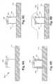
- Two gatesmay be defined in the gate material layer 320 by lithography (e.g., photolithography). Gate material layer 320 may be selectively etched to form a gate structure out of the gate material layer 320 on device 100 . Forming the gate structure in such a manner may leave some gate material 320 on top of the dielectric cap 140 , for example as illustrated in FIG. 3.
- lithographye.g., photolithography
- FIG. 4is a cross-section illustrating the planarizing of the gate material 320 in accordance with an exemplary embodiment of the present invention.
- Excess gate materialmay be removed (e.g., from above the dielectric cap 140 ) to planarize the fin region of the semiconductor device 100 .
- CMPchemical-mechanical polishing
- CMPmay be performed so that the gate material (i.e., layer 320 ) is even with or nearly even with dielectric cap 140 in the vertical direction, as illustrated in FIG. 4.
- the gate material layer 320 in the channel region of semiconductor device 100abuts fin 210 on the two side surfaces to form a first gate 410 and a second gate 420 .
- the top surface of fin 210is covered by dielectric cap 140 .
- FIG. 5illustrates a top view of semiconductor device 100 consistent with the present invention.
- first gate 410 and second gate 420are shown adjacent, but not covering, fin 210 .
- the gate material layer 320may then be patterned and etched to form two gate electrodes. As illustrated in FIG. 5, semiconductor device 100 includes a double gate structure with gate electrodes 510 and 520 . Gate electrodes 510 and 520 are effectively separated by fin 210 and may be separately biased, as discussed in more detail below.
- the gate dielectric 310(FIG. 4) surrounding the side surfaces of fin 210 is not shown in FIG. 5 for simplicity.
- the source/drain regions 220 and 230may then be doped. For example, n-type or p-type impurities may be implanted in source/drain regions 220 and 230 .
- the particular implantation dosages and energiesmay be selected based on the particular end device requirements. One or ordinary skill in this art would be able to optimize the source/drain implantation process based on the circuit requirements and such steps are not disclosed herein in order not to unduly obscure the thrust of the present invention.
- sidewall spacers(not shown) may optionally be formed prior to the source/drain ion implantation to control the location of the source/drain junctions based on the particular circuit requirements. Activation annealing may then be performed to activate the source/drain regions 220 and 230 .
- gate electrode 510 and gate electrode 520are physically and electrically separated from each other.
- each of the gate electrodes 510 and 520may be separately biased with different voltages when used in a circuit.
- the capability for independently biasing the gates 410 and 420 (via gate electrodes 510 and 520 )increases the flexibility of circuit design using semiconductor device 100 .
- the resulting semiconductor device 100 illustrated in FIG. 5is a double gate device with a first gate 410 and a second gate 420 .
- the gate material layer 320(FIGS. 3 and 4) abuts two surfaces of fin 210 and provides semiconductor device 100 with increased channel width per device, as compared to a conventional double gate device.
- the fin 210may also retain the dielectric cap 140 that protects the fin 210 during gate etching.
- the gates 410 and 420are also effectively separated by fin 210 and may be separately biased (via respective gate electrodes 510 and 520 ) based on the particular circuit requirements of device 100 .
- This separate double gate structureprovides increased flexibility during circuit design, as opposed to conventional FinFETs which include a single gate connection.
- a double-gate FinFET deviceis formed with two separate gates in the channel region of the device.
- the resulting structureexhibits good short channel behavior.
- the present inventionprovides increased flexibility and can be easily integrated into conventional processing.
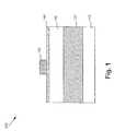
- FIGS. 6 A- 6 Dare cross-sections illustrating the induction of tensile strain in a fin in accordance with another implementation of the present invention.
- FIG. 6Aillustrates the cross-section of a semiconductor device 600 .
- device 600may include a buried oxide (BOX) layer 610 , a fin 620 , and an SiO 2 cap 630 .
- Elements 610 - 630may be formed as described above with respect to FIGS. 1 - 2 B.
- Fin 620may include silicon, germanium or a combination of silicon and germanium.
- a thick sacrificial oxide layer 640may be thermally grown on fin 620 as shown in FIG. 6B. Growing the thick (e.g., 200-400 ⁇ ) sacrificial oxide layer 640 may induce a tensile strain in fin 620 . The sacrificial oxide layer 640 may then be removed, and a thin gate oxide layer 650 may be grown, as illustrated in FIG. 6C. Gate material 660 may then be deposited over the fin 620 as shown in FIG. 6D.
- a FinFETmay be formed from the structure in FIG. 6D in a typical manner. The fin 620 in such a FinFET will have a tensile strain, imparting qualities to the fin 620 that will be understood by those skilled in the art.
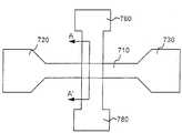
- FIGS. 7A and 7Bare views illustrating exemplary processing for forming a FinFET with a fully silicided gate.
- device 700includes a fin 710 , source region 720 , and drain region 730 . These layers/structures may be formed as described above with respect to FIGS. 1 - 2 B.
- fin 710may include a top oxide cap 740 and gate oxide 750 surrounding a silicon structure. Fin 710 may be formed on a buried oxide (BOX) layer 705 .
- BOXburied oxide
- a thin polysilicon layer 760may be deposited on the fin 710 , as shown in FIG. 7C. Then a thick bottom antireflective (BARC) layer 770 may be deposited, as shown in FIG. 7D. The gate region and contacts 780 may then be patterned and etched as shown from the top in FIG. 7E.
- BARCbottom antireflective
- Source and drain regions 720 and 730may be implanted with ions without removing the BARC layer 770 . Thus, the dopants used will be stopped by the BARC layer 770 from penetrating into the channel (e.g., fin 710 ).
- BARC layer 770may be removed, and the polysilicon 760 is fully silicided to form a metal gate 780 , as illustrated in FIGS. 7E and 7F.
- the gate material 710may also be planarized in a manner similar to that described above with respect to FIG. 4.
- the dielectric and conductive layers used in manufacturing a semiconductor device in accordance with the present inventioncan be deposited by conventional deposition techniques.
- metallization techniquesSuch as various types of CVD processes, including low pressure CVD (LPCVD) and enhanced CVD (ECVD) can be employed.
- LPCVDlow pressure CVD
- ECVDenhanced CVD
- the present inventionis applicable in the manufacturing of double-gate semiconductor devices and particularly in FinFET devices with design features of 100 nm and below.
- the present inventionis applicable to the formation of any of various types of semiconductor devices, and hence, details have not been set forth in order to avoid obscuring the thrust of the present invention.
- conventional photolithographic and etching techniquesare employed and, hence, the details of such techniques have not been set forth herein in detail.
Landscapes
- Thin Film Transistor (AREA)
- Insulated Gate Type Field-Effect Transistor (AREA)
- Testing Or Measuring Of Semiconductors Or The Like (AREA)
Abstract
Description
- The present invention relates to semiconductor devices and methods of manufacturing semiconductor devices. The present invention has particular applicability to double-gate devices.[0001]
- The escalating requirements for high density and performance associated with ultra large scale integration semiconductor devices require design features, such as gate lengths, below 100 nanometers (nm), high reliability and increased manufacturing throughput. The reduction of design features below 100 nm challenges the limitations of conventional methodology.[0002]
- For example, when the gate length of conventional planar metal oxide semiconductor field effect transistors (MOSFETs) is scaled below 100 μm, problems associated with short channel effects, such as excessive leakage between the source and drain, become increasingly difficult to overcome. In addition, mobility degradation and a number of process issues also make it difficult to scale conventional MOSFETs to include increasingly smaller device features. New device structures are therefore being explored to improve FET performance and allow further device scaling.[0003]
- Double-gate MOSFETs represent new structures that have been considered as candidates for succeeding existing planar MOSFETs. In several respects, the double-gate MOSFETs offer better characteristics than the conventional bulk silicon MOSFETs. These improvements arise because the double-gate MOSFET has a gate electrode on both sides of the channel, rather than only on one side as in conventional MOSFETs. When there are two gates, the electric field generated by the drain is better screened from the source end of the channel. Also, two gates can control roughly twice as much current as a single gate, resulting in a stronger switching signal.[0004]
- FinFET is a recent double-gate structure that exhibits good short channel behavior. Although conventional FinFETs are referred to as “double-gate” MOSFETs, the two gates typically are physically and electrically connected and thus form a single logically addressable gate. A FinFET includes a channel formed in a vertical fin. The FinFET structure may be fabricated using layout and process techniques similar to those used for conventional planar MOSFETs.[0005]
- Implementations consistent with the present invention provide a FinFET device with two gates that are effectively separated from each other by a conductive fin. The gates may be independently biased for increased circuit design flexibility.[0006]
- Additional advantages and other features of the invention will be set forth in part in the description which follows and in part will become apparent to those having ordinary skill in the art upon examination of the following or may be learned from the practice of the invention. The advantages and features of the invention may be realized and obtained as particularly pointed out in the appended claims.[0007]
- According to the present invention, the foregoing and other advantages are achieved in part by a semiconductor device including a substrate and an insulating layer formed on the substrate. A fin may be formed on the insulating layer and may include a number of side surfaces and a top surface. A first gate may be formed on the insulating layer proximate to one of number of side surfaces of the fin. A second gate may be formed on the insulating layer separate from the first gate and proximate to another one of number of side surfaces of the fin.[0008]
- According to another aspect of the invention, a method of manufacturing a semiconductor device may include forming an insulating layer on a substrate and forming a fin stricture on the insulating layer. The fin structure includes a first side surface, a second side surface, and a top surface. The method may also include forming source and drain regions at ends of the fin structure and depositing a gate material over the fin structure. The gate material surrounds the top surface and the first and second side surfaces. The gate material may be etched to form a first gate electrode and a second gate electrode on opposite sides of the fin. The deposited gate material may be planarized proximate to the fin.[0009]
- According to a further aspect of the invention a semiconductor device may include a substrate and an insulating layer formed on the substrate. A conductive fin may be formed on the insulating layer, and gate dielectric layers may be formed on side surfaces of the conductive fin. A first gate electrode may be formed on the insulating layer. The first gate electrode may be disposed on a first side of the conductive fin adjacent to one of the gate dielectric layers. A second gate electrode may be formed on the insulating layer. The second gate electrode may be disposed on an opposite side of the conductive fin adjacent to another one of the gate dielectric layers and spaced apart from the first gate electrode.[0010]
- Other advantages and features of the present invention will become readily apparent to those skilled in this art from the following detailed description. The embodiments shown and described provide illustration of the best mode contemplated for carrying out the invention. The invention is capable of modifications in various obvious respects, all without departing from the invention. Accordingly, the drawings are to be regarded as illustrative in nature, and not as restrictive.[0011]
- Reference is made to the attached drawings, wherein elements having the same reference number designation may represent like elements throughout.[0012]
- FIG. 1 is a cross-section illustrating exemplary layers that may be used for forming a fin in accordance with an embodiment of the present invention.[0013]
- FIG. 2A schematically illustrates the top view of a fin structure in accordance with an exemplary embodiment of the present invention.[0014]
- FIG. 2B is a cross-section illustrating the fin structure of FIG. 2A in accordance with an exemplary embodiment of the present invention.[0015]
- FIG. 3 is a cross-section illustrating the formation of a gate dielectric layer and gate material on the device of FIG. 2B in accordance with an exemplary embodiment of the present invention.[0016]
- FIG. 4 is a cross-section illustrating the planarizing of the gate material of FIG. 3 in accordance with an exemplary embodiment of the present invention.[0017]
- FIG. 5 schematically illustrates the top view of the semiconductor device of FIG. 4 in accordance with an exemplary embodiment of the present invention.[0018]
- FIGS.[0019]6A-6D are cross-sections illustrating the induction of tensile strain in a fin in accordance with another implementation of the present invention.
- FIGS.[0020]7A-7F are top and cross-sectional views illustrating formation of a fully silicided gate in a FinFET in accordance with another implementation of the present invention.
- The following detailed description of the invention refers to the accompanying drawings. The same reference numbers in different drawings may identify the same or similar elements. Also, the following detailed description does not limit the invention. Instead, the scope of the invention is defined by the appended claims and their equivalents.[0021]
- Implementations consistent with the present invention provide double gate FinFET devices and methods of manufacturing such devices. The gates in the FinFET devices formed in accordance with the present invention are effectively separated from each other and may be separately biased.[0022]
- FIG. 1 illustrates the cross-section of a[0023]
semiconductor device 100 formed in accordance with an embodiment of the present invention. Referring to FIG. 1,semiconductor device 100 may include a silicon on insulator (SOI) structure that includes asilicon substrate 110, a buriedoxide layer 120 and asilicon layer 130 on the buriedoxide layer 120.Buried oxide layer 120 andsilicon layer 130 may be formed onsubstrate 110 in a conventional manner. - In an exemplary implementation, buried[0024]
oxide layer 120 may include a silicon oxide and may have a thickness ranging from about 1000 Å to about 3000 Å.Silicon layer 130 may include monocrystalline or polycrystalline silicon having a thickness ranging from about 300 Å to about 1500 Å.Silicon layer 130 is used to form a fin structure for a double gate transistor device, as described in more detail below. - In alternative implementations consistent with the present invention,[0025]
substrate 110 andlayer 130 may include other semiconducting materials, such as germanium, or combinations of semiconducting materials, such as silicon-germanium.Buried oxide layer 120 may also include other dielectric materials. - A[0026]
dielectric layer 140, such as a silicon nitride layer or a silicon oxide layer (e.g., SiO2), may be formed oversilicon layer 130 to act as a protective cap during subsequent etching processes. In an exemplary implementation,dielectric layer 140 may be deposited at a thickness ranging from about 150 Å to about 600 Å. Next, a photoresist material may be deposited and patterned to form aphotoresist mask 150 for subsequent processing. The photoresist may be deposited and patterned in any conventional manner. - [0027]
Semiconductor device 100 may then be etched and thephotoresist mask 150 may be removed. In an exemplary implementation,silicon layer 130 may be etched in a conventional manner, with the etching terminating on buriedoxide layer 120 to form a fin. After the formation of the fin, source and drain regions may be formed adjacent the respective ends of the fin. For example, in an exemplary embodiment, a layer of silicon, germanium or combination of silicon and germanium may be deposited, patterned and etched in a conventional manner to form source and drain regions. - FIG. 2A schematically illustrates the top view of a fin structure on[0028]
semiconductor 100 formed in such a manner.Source region 220 and drainregion 230 may be formed adjacent the ends offin 210 on buriedoxide layer 120, according to an exemplary embodiment of the present invention. - FIG. 2B is a cross-section along line A-A′ in FIG. 2A illustrating the fin structure in accordance with an exemplary embodiment of the present invention.[0029]
Dielectric layer 140 andsilicon layer 130 have been etched to formfin 210.Fin 210 may includesilicon 130 and adielectric cap 140. - FIG. 3 is a cross-section illustrating the formation of a gate dielectric layer and gate material on[0030]
fin 210 in accordance with an exemplary embodiment of the present invention. A dielectric layer may be formed onfin 210. For example, athin oxide film 310 may be thermally grown onfin 210, as illustrated in FIG. 4. Theoxide film 310 may be grown to a thickness of about 10 Å to about 50 Å and may be formed on the exposed side surfaces ofsilicon 130 infin 210 to act as a dielectric layer for a subsequently formed gate electrode. Similar to theoxide film 310, thedielectric cap 140 may provide electrical insulation for the top surface offin 210. - A[0031]
gate material layer 320 may be deposited oversemiconductor device 100 after formation of theoxide film 310. Thegate material layer 320 may comprise the material for the subsequently formed gate electrode. In an exemplary implementation, thegate material layer 320 may include polysilicon deposited using conventional chemical vapor deposition (CVD) to a thickness ranging from about 300 Å to about 1500 Å. Alternatively, other semiconducting materials, such as germanium or combinations of silicon and germanium, or various metals may be used as the gate material. - Two gates may be defined in the[0032]
gate material layer 320 by lithography (e.g., photolithography).Gate material layer 320 may be selectively etched to form a gate structure out of thegate material layer 320 ondevice 100. Forming the gate structure in such a manner may leave somegate material 320 on top of thedielectric cap 140, for example as illustrated in FIG. 3. - FIG. 4 is a cross-section illustrating the planarizing of the[0033]
gate material 320 in accordance with an exemplary embodiment of the present invention. Excess gate material may be removed (e.g., from above the dielectric cap140) to planarize the fin region of thesemiconductor device 100. For example, chemical-mechanical polishing (CMP) may be performed so that the gate material (i.e., layer320) is even with or nearly even withdielectric cap 140 in the vertical direction, as illustrated in FIG. 4. - Referring to FIG. 4, the[0034]
gate material layer 320 in the channel region ofsemiconductor device 100 abutsfin 210 on the two side surfaces to form afirst gate 410 and asecond gate 420. The top surface offin 210, however, is covered bydielectric cap 140. This structure is also shown in FIG. 5, which illustrates a top view ofsemiconductor device 100 consistent with the present invention. In FIG. 5,first gate 410 andsecond gate 420 are shown adjacent, but not covering,fin 210. - The[0035]
gate material layer 320 may then be patterned and etched to form two gate electrodes. As illustrated in FIG. 5,semiconductor device 100 includes a double gate structure withgate electrodes 510 and520.Gate electrodes 510 and520 are effectively separated byfin 210 and may be separately biased, as discussed in more detail below. The gate dielectric310 (FIG. 4) surrounding the side surfaces offin 210 is not shown in FIG. 5 for simplicity. - The source/[0036]
drain regions drain regions drain regions - As illustrated in FIG. 5, gate electrode[0037]510 and
gate electrode 520 are physically and electrically separated from each other. In accordance with an exemplary embodiment of the present invention, each of thegate electrodes 510 and520 may be separately biased with different voltages when used in a circuit. The capability for independently biasing thegates 410 and420 (via gate electrodes510 and520) increases the flexibility of circuit design usingsemiconductor device 100. - The resulting[0038]
semiconductor device 100 illustrated in FIG. 5 is a double gate device with afirst gate 410 and asecond gate 420. The gate material layer320 (FIGS. 3 and 4) abuts two surfaces offin 210 and providessemiconductor device 100 with increased channel width per device, as compared to a conventional double gate device. Thefin 210 may also retain thedielectric cap 140 that protects thefin 210 during gate etching. - The[0039]
gates fin 210 and may be separately biased (via respective gate electrodes510 and520) based on the particular circuit requirements ofdevice 100. This separate double gate structure provides increased flexibility during circuit design, as opposed to conventional FinFETs which include a single gate connection. - Thus, in accordance with the present invention, a double-gate FinFET device is formed with two separate gates in the channel region of the device. Advantageously, the resulting structure exhibits good short channel behavior. In addition, the present invention provides increased flexibility and can be easily integrated into conventional processing.[0040]
- In some implementations, it may be desirable to induce tensile strain in the fin of a FinFET. FIGS.[0041]6A-6D are cross-sections illustrating the induction of tensile strain in a fin in accordance with another implementation of the present invention. FIG. 6A illustrates the cross-section of a
semiconductor device 600. Referring to FIG. 6A,device 600 may include a buried oxide (BOX)layer 610, afin 620, and an SiO2cap630. Elements610-630 may be formed as described above with respect to FIGS.1-2B.Fin 620 may include silicon, germanium or a combination of silicon and germanium. - A thick[0042]
sacrificial oxide layer 640 may be thermally grown onfin 620 as shown in FIG. 6B. Growing the thick (e.g., 200-400 Å)sacrificial oxide layer 640 may induce a tensile strain infin 620. Thesacrificial oxide layer 640 may then be removed, and a thingate oxide layer 650 may be grown, as illustrated in FIG. 6C.Gate material 660 may then be deposited over thefin 620 as shown in FIG. 6D. A FinFET may be formed from the structure in FIG. 6D in a typical manner. Thefin 620 in such a FinFET will have a tensile strain, imparting qualities to thefin 620 that will be understood by those skilled in the art. - In other implementations, a FinFET with a fully silicided gate may be desired. Such a FinFET may have an incorporated metal gate that removes a polysilicon depletion effect and helps to achieve a proper threshold voltage for the FinFET. FIGS. 7A and 7B are views illustrating exemplary processing for forming a FinFET with a fully silicided gate. Referring to FIG. 7A,[0043]
device 700 includes afin 710,source region 720, and drainregion 730. These layers/structures may be formed as described above with respect to FIGS.1-2B. As shown in FIG. 7B,fin 710 may include atop oxide cap 740 andgate oxide 750 surrounding a silicon structure.Fin 710 may be formed on a buried oxide (BOX)layer 705. - A[0044]
thin polysilicon layer 760 may be deposited on thefin 710, as shown in FIG. 7C. Then a thick bottom antireflective (BARC)layer 770 may be deposited, as shown in FIG. 7D. The gate region andcontacts 780 may then be patterned and etched as shown from the top in FIG. 7E. - Source and[0045]
drain regions BARC layer 770. Thus, the dopants used will be stopped by theBARC layer 770 from penetrating into the channel (e.g., fin710). - [0046]
BARC layer 770 may be removed, and thepolysilicon 760 is fully silicided to form ametal gate 780, as illustrated in FIGS. 7E and 7F. Thegate material 710 may also be planarized in a manner similar to that described above with respect to FIG. 4. - In the previous descriptions, numerous specific details are set forth, such as specific materials, structures, chemicals, processes, etc., in order to provide a thorough understanding of the present invention. However, the present invention can be practiced without resorting to the specific details set forth herein. In other instances, well known processing structures have not been described in detail, in order not to unnecessarily obscure the thrust of the present invention.[0047]
- The dielectric and conductive layers used in manufacturing a semiconductor device in accordance with the present invention can be deposited by conventional deposition techniques. For example, metallization techniques, Such as various types of CVD processes, including low pressure CVD (LPCVD) and enhanced CVD (ECVD) can be employed.[0048]
- The present invention is applicable in the manufacturing of double-gate semiconductor devices and particularly in FinFET devices with design features of 100 nm and below. The present invention is applicable to the formation of any of various types of semiconductor devices, and hence, details have not been set forth in order to avoid obscuring the thrust of the present invention. In practicing the present invention, conventional photolithographic and etching techniques are employed and, hence, the details of such techniques have not been set forth herein in detail.[0049]
- Only the preferred embodiments of the invention and a few examples of its versatility are shown and described in the present disclosure. It is to be understood that the invention is capable of use in various other combinations and environments and is capable of modifications within the scope of the inventive concept as expressed herein.[0050]
Claims (20)
1. A semiconductor device, comprising:
a substrate;
an insulating layer formed on the substrate;
a fin formed on the insulating layer and including a plurality of side surfaces and a top surface;
a first gate formed on the insulating layer proximate to one of plurality of side surfaces of the fin; and
a second gate formed on the insulating layer separate from the first gate and proximate to another one of plurality of side surfaces of the fin.
2. The semiconductor device ofclaim 1 wherein the second gate is formed at an opposite side of the fin from the first gate.
3. The semiconductor device ofclaim 2 , wherein the first and second gates respectively include first and second gate contacts.
4. The semiconductor device ofclaim 1 , further comprising:
a plurality of dielectric layers respectively formed along the plurality of side surfaces of the fin.
5. The semiconductor device ofclaim 4 , wherein the first and second gates respectively abut different ones of the plurality of dielectric layers.
6. The semiconductor device ofclaim 1 , wherein the fin comprises at least one of silicon and germanium.
7. The semiconductor device ofclaim 1 , wherein the insulating layer comprises a buried oxide layer.
8. The semiconductor device ofclaim 1 , further comprising:
a source region and a drain region formed above the insulating layer and adjacent a respective first and second end of the fin.
9. The semiconductor device ofclaim 1 , further comprising:
a dielectric layer comprising at least one of a nitride and an oxide formed over the top surface of the fin.
10. The semiconductor device ofclaim 9 , wherein a top surface of the dielectric layer, a top surface of the first gate, and a top surface of the second gate are substantially coplanar.
11. A method of manufacturing a semiconductor device, comprising:
forming an insulating layer on a substrate;
forming a fin structure on the insulating layer, the fin structure including a first side surface, a second side surface, and a top surface;
forming source and drain regions at ends of the fin structure;
depositing a gate material over the fin structure, the gate material surrounding the top surface and the first and second side surfaces;
etching the gate material to form a first gate electrode and a second gate electrode on opposite sides of the tin; and
planarizing the deposited gate material proximate to the fin.
12. The method ofclaim 11 , further comprising:
implanting impurities in the source and drain regions; and
annealing the semiconductor device to activate the source and drain regions.
13. The method ofclaim 11 , further comprising:
forming a dielectric layer over the top surface of the fin structure.
14. The method ofclaim 13 , wherein the planarizing includes:
polishing the gate material so that no gate material remains above the dielectric layer.
15. The method ofclaim 11 , further comprising:
growing oxide layers on the first side surface and the second side surface of the fin structure.
16. A semiconductor device, comprising:
a substrate;
an insulating layer formed on the substrate;
a conductive fin formed on the insulating layer;
gate dielectric layers formed on side surfaces of the conductive fin;
a first gate electrode formed on the insulating layer, the first gate electrode disposed on a first side of the conductive fin adjacent one of the gate dielectric layers; and
a second gate electrode formed on the insulating layer, the second gate electrode disposed on an opposite side of the conductive fin adjacent another one of the gate dielectric layers and spaced apart from the first gate electrode.
17. The semiconductor device ofclaim 16 , further comprising:
a dielectric cap formed over a top surface of the conductive fin.
18. The semiconductor device ofclaim 17 , wherein neither of the first gate electrode and the second gate electrode extend over the dielectric cap.
19. The semiconductor device ofclaim 17 , wherein top surfaces of the first gate electrode, the second gate electrode, and the dielectric cap are substantially coplanar.
20. The semiconductor device ofclaim 16 , wherein the first gate electrode and the second gate electrode are aligned on opposite sides of the conductive fin and are not electrically connected to each other.
Priority Applications (1)
| Application Number | Priority Date | Filing Date | Title |
|---|---|---|---|
| US10/602,061US20040126975A1 (en) | 2002-11-08 | 2003-06-24 | Double gate semiconductor device having separate gates |
Applications Claiming Priority (2)
| Application Number | Priority Date | Filing Date | Title |
|---|---|---|---|
| US10/290,158US6611029B1 (en) | 2002-11-08 | 2002-11-08 | Double gate semiconductor device having separate gates |
| US10/602,061US20040126975A1 (en) | 2002-11-08 | 2003-06-24 | Double gate semiconductor device having separate gates |
Related Parent Applications (1)
| Application Number | Title | Priority Date | Filing Date |
|---|---|---|---|
| US10/290,158DivisionUS6611029B1 (en) | 2002-11-08 | 2002-11-08 | Double gate semiconductor device having separate gates |
Publications (1)
| Publication Number | Publication Date |
|---|---|
| US20040126975A1true US20040126975A1 (en) | 2004-07-01 |
Family
ID=27757499
Family Applications (2)
| Application Number | Title | Priority Date | Filing Date |
|---|---|---|---|
| US10/290,158Expired - LifetimeUS6611029B1 (en) | 2002-11-08 | 2002-11-08 | Double gate semiconductor device having separate gates |
| US10/602,061AbandonedUS20040126975A1 (en) | 2002-11-08 | 2003-06-24 | Double gate semiconductor device having separate gates |
Family Applications Before (1)
| Application Number | Title | Priority Date | Filing Date |
|---|---|---|---|
| US10/290,158Expired - LifetimeUS6611029B1 (en) | 2002-11-08 | 2002-11-08 | Double gate semiconductor device having separate gates |
Country Status (9)
| Country | Link |
|---|---|
| US (2) | US6611029B1 (en) |
| JP (1) | JP2006505950A (en) |
| KR (1) | KR101029383B1 (en) |
| CN (1) | CN100459166C (en) |
| AU (1) | AU2003291641A1 (en) |
| DE (1) | DE10393687B4 (en) |
| GB (1) | GB2408849B (en) |
| TW (1) | TWI311371B (en) |
| WO (1) | WO2004044992A1 (en) |
Cited By (33)
| Publication number | Priority date | Publication date | Assignee | Title |
|---|---|---|---|---|
| US20040036126A1 (en)* | 2002-08-23 | 2004-02-26 | Chau Robert S. | Tri-gate devices and methods of fabrication |
| US20050156171A1 (en)* | 2003-12-30 | 2005-07-21 | Brask Justin K. | Nonplanar transistors with metal gate electrodes |
| US20050158970A1 (en)* | 2004-01-16 | 2005-07-21 | Robert Chau | Tri-gate transistors and methods to fabricate same |
| US20050193143A1 (en)* | 2003-12-30 | 2005-09-01 | Meyers Brian R. | Framework for user interaction with multiple network devices |
| US20050218438A1 (en)* | 2004-03-31 | 2005-10-06 | Nick Lindert | Bulk non-planar transistor having strained enhanced mobility and methods of fabrication |
| US20060063332A1 (en)* | 2004-09-23 | 2006-03-23 | Brian Doyle | U-gate transistors and methods of fabrication |
| US20060068550A1 (en)* | 2004-09-29 | 2006-03-30 | Intel Corporation | Independently accessed double-gate and tri-gate transistors in same process flow |
| US20060138553A1 (en)* | 2004-09-30 | 2006-06-29 | Brask Justin K | Nonplanar transistors with metal gate electrodes |
| US20060157794A1 (en)* | 2005-01-18 | 2006-07-20 | Doyle Brian S | Non-planar MOS structure with a strained channel region |
| US20060172497A1 (en)* | 2003-06-27 | 2006-08-03 | Hareland Scott A | Nonplanar semiconductor device with partially or fully wrapped around gate electrode and methods of fabrication |
| US7091068B1 (en)* | 2002-12-06 | 2006-08-15 | Advanced Micro Devices, Inc. | Planarizing sacrificial oxide to improve gate critical dimension in semiconductor devices |
| US20060186484A1 (en)* | 2005-02-23 | 2006-08-24 | Chau Robert S | Field effect transistor with narrow bandgap source and drain regions and method of fabrication |
| US20060214231A1 (en)* | 2004-10-25 | 2006-09-28 | Uday Shah | Nonplanar device with thinned lower body portion and method of fabrication |
| US20060261411A1 (en)* | 2003-06-27 | 2006-11-23 | Hareland Scott A | Nonplanar device with stress incorporation layer and method of fabrication |
| US20070001219A1 (en)* | 2005-06-30 | 2007-01-04 | Marko Radosavljevic | Block contact architectures for nanoscale channel transistors |
| US20070040223A1 (en)* | 2005-08-17 | 2007-02-22 | Intel Corporation | Lateral undercut of metal gate in SOI device |
| US20070063230A1 (en)* | 2005-09-19 | 2007-03-22 | International Business Machines Corporation | Asymmetrically stressed cmos finfet |
| US20070090416A1 (en)* | 2005-09-28 | 2007-04-26 | Doyle Brian S | CMOS devices with a single work function gate electrode and method of fabrication |
| US20070148837A1 (en)* | 2005-12-27 | 2007-06-28 | Uday Shah | Method of fabricating a multi-cornered film |
| US7348284B2 (en) | 2004-08-10 | 2008-03-25 | Intel Corporation | Non-planar pMOS structure with a strained channel region and an integrated strained CMOS flow |
| US20080160684A1 (en)* | 2004-06-29 | 2008-07-03 | Samsung Electronics Co., Ltd. | Method of fabricating multi-gate transistor and multi-gate transistor fabricated thereby |
| US20080164535A1 (en)* | 2007-01-09 | 2008-07-10 | Dureseti Chidambarrao | Curved finfets |
| US7479421B2 (en) | 2005-09-28 | 2009-01-20 | Intel Corporation | Process for integrating planar and non-planar CMOS transistors on a bulk substrate and article made thereby |
| US7547637B2 (en) | 2005-06-21 | 2009-06-16 | Intel Corporation | Methods for patterning a semiconductor film |
| US7579280B2 (en) | 2004-06-01 | 2009-08-25 | Intel Corporation | Method of patterning a film |
| US20100065888A1 (en)* | 2004-06-30 | 2010-03-18 | Shaheen Mohamad A | High mobility tri-gate devices and methods of fabrication |
| US7858481B2 (en) | 2005-06-15 | 2010-12-28 | Intel Corporation | Method for fabricating transistor with thinned channel |
| US7879675B2 (en) | 2005-03-14 | 2011-02-01 | Intel Corporation | Field effect transistor with metal source/drain regions |
| US7915167B2 (en) | 2004-09-29 | 2011-03-29 | Intel Corporation | Fabrication of channel wraparound gate structure for field-effect transistor |
| US7989280B2 (en) | 2005-11-30 | 2011-08-02 | Intel Corporation | Dielectric interface for group III-V semiconductor device |
| US8362566B2 (en) | 2008-06-23 | 2013-01-29 | Intel Corporation | Stress in trigate devices using complimentary gate fill materials |
| US8617945B2 (en) | 2006-08-02 | 2013-12-31 | Intel Corporation | Stacking fault and twin blocking barrier for integrating III-V on Si |
| US9525072B2 (en) | 2014-08-11 | 2016-12-20 | Taiwan Semiconductor Manufacturing Company Limited | Semiconductor device and method of formation |
Families Citing this family (76)
| Publication number | Priority date | Publication date | Assignee | Title |
|---|---|---|---|---|
| US6982460B1 (en)* | 2000-07-07 | 2006-01-03 | International Business Machines Corporation | Self-aligned gate MOSFET with separate gates |
| US6800910B2 (en)* | 2002-09-30 | 2004-10-05 | Advanced Micro Devices, Inc. | FinFET device incorporating strained silicon in the channel region |
| US6611029B1 (en)* | 2002-11-08 | 2003-08-26 | Advanced Micro Devices, Inc. | Double gate semiconductor device having separate gates |
| US6815268B1 (en)* | 2002-11-22 | 2004-11-09 | Advanced Micro Devices, Inc. | Method for forming a gate in a FinFET device |
| US6855990B2 (en)* | 2002-11-26 | 2005-02-15 | Taiwan Semiconductor Manufacturing Co., Ltd | Strained-channel multiple-gate transistor |
| US7001837B2 (en)* | 2003-01-17 | 2006-02-21 | Advanced Micro Devices, Inc. | Semiconductor with tensile strained substrate and method of making the same |
| US7148526B1 (en) | 2003-01-23 | 2006-12-12 | Advanced Micro Devices, Inc. | Germanium MOSFET devices and methods for making same |
| US6803631B2 (en)* | 2003-01-23 | 2004-10-12 | Advanced Micro Devices, Inc. | Strained channel finfet |
| US6855606B2 (en)* | 2003-02-20 | 2005-02-15 | Taiwan Semiconductor Manufacturing Company, Ltd. | Semiconductor nano-rod devices |
| US7074656B2 (en)* | 2003-04-29 | 2006-07-11 | Taiwan Semiconductor Manufacturing Company, Ltd. | Doping of semiconductor fin devices |
| US7029959B1 (en)* | 2003-05-06 | 2006-04-18 | Advanced Micro Devices, Inc. | Source and drain protection and stringer-free gate formation in semiconductor devices |
| US6756643B1 (en) | 2003-06-12 | 2004-06-29 | Advanced Micro Devices, Inc. | Dual silicon layer for chemical mechanical polishing planarization |
| US6913959B2 (en)* | 2003-06-23 | 2005-07-05 | Advanced Micro Devices, Inc. | Method of manufacturing a semiconductor device having a MESA structure |
| US7087506B2 (en)* | 2003-06-26 | 2006-08-08 | International Business Machines Corporation | Method of forming freestanding semiconductor layer |
| US7005330B2 (en)* | 2003-06-27 | 2006-02-28 | Taiwan Semiconductor Manufacturing Company, Ltd. | Structure and method for forming the gate electrode in a multiple-gate transistor |
| US7078742B2 (en)* | 2003-07-25 | 2006-07-18 | Taiwan Semiconductor Manufacturing Co., Ltd. | Strained-channel semiconductor structure and method of fabricating the same |
| US7301206B2 (en)* | 2003-08-01 | 2007-11-27 | Taiwan Semiconductor Manufacturing Company, Ltd. | Semiconductor-on-insulator SRAM configured using partially-depleted and fully-depleted transistors |
| US7355253B2 (en)* | 2003-08-22 | 2008-04-08 | International Business Machines Corporation | Strained-channel Fin field effect transistor (FET) with a uniform channel thickness and separate gates |
| US8008136B2 (en)* | 2003-09-03 | 2011-08-30 | Advanced Micro Devices, Inc. | Fully silicided gate structure for FinFET devices |
| US6970373B2 (en)* | 2003-10-02 | 2005-11-29 | Intel Corporation | Method and apparatus for improving stability of a 6T CMOS SRAM cell |
| US7888201B2 (en)* | 2003-11-04 | 2011-02-15 | Taiwan Semiconductor Manufacturing Company, Ltd. | Semiconductor-on-insulator SRAM configured using partially-depleted and fully-depleted transistors |
| US8217450B1 (en) | 2004-02-03 | 2012-07-10 | GlobalFoundries, Inc. | Double-gate semiconductor device with gate contacts formed adjacent sidewalls of a fin |
| US7060539B2 (en)* | 2004-03-01 | 2006-06-13 | International Business Machines Corporation | Method of manufacture of FinFET devices with T-shaped fins and devices manufactured thereby |
| KR100620446B1 (en)* | 2004-03-09 | 2006-09-12 | 삼성전자주식회사 | Fin Field Effect Transistor and Method of Manufacturing the Same |
| US7262084B2 (en)* | 2004-04-15 | 2007-08-28 | International Business Machines Corporation | Methods for manufacturing a finFET using a conventional wafer and apparatus manufactured therefrom |
| US7098477B2 (en)* | 2004-04-23 | 2006-08-29 | International Business Machines Corporation | Structure and method of manufacturing a finFET device having stacked fins |
| KR100634372B1 (en)* | 2004-06-04 | 2006-10-16 | 삼성전자주식회사 | Semiconductor Devices and Formation Methods |
| US7452778B2 (en)* | 2004-06-10 | 2008-11-18 | Taiwan Semiconductor Manufacturing Company, Ltd. | Semiconductor nano-wire devices and methods of fabrication |
| US7084461B2 (en)* | 2004-06-11 | 2006-08-01 | International Business Machines Corporation | Back gate FinFET SRAM |
| US8669145B2 (en)* | 2004-06-30 | 2014-03-11 | International Business Machines Corporation | Method and structure for strained FinFET devices |
| KR100618852B1 (en) | 2004-07-27 | 2006-09-01 | 삼성전자주식회사 | Semiconductor device with high operating current |
| US6951784B1 (en) | 2004-08-05 | 2005-10-04 | International Business Machines Corporation | Three-mask method of constructing the final hard mask used for etching the silicon fins for FinFETs |
| US7348641B2 (en)* | 2004-08-31 | 2008-03-25 | International Business Machines Corporation | Structure and method of making double-gated self-aligned finFET having gates of different lengths |
| US7241649B2 (en)* | 2004-10-29 | 2007-07-10 | International Business Machines Corporation | FinFET body contact structure |
| WO2006076151A2 (en)* | 2004-12-21 | 2006-07-20 | Carnegie Mellon University | Lithography and associated methods, devices, and systems |
| US7288805B2 (en)* | 2005-02-24 | 2007-10-30 | International Business Machines Corporation | Double gate isolation |
| DE602005014394D1 (en)* | 2005-06-16 | 2009-06-18 | Vkr Holding As | SOLAR PANEL |
| US7411252B2 (en)* | 2005-06-21 | 2008-08-12 | International Business Machines Corporation | Substrate backgate for trigate FET |
| CN100442295C (en)* | 2005-08-05 | 2008-12-10 | 中芯国际集成电路制造(上海)有限公司 | Static method and system for basic knowledge for determining semiconductor IC credibility and comparison |
| US7566609B2 (en)* | 2005-11-29 | 2009-07-28 | International Business Machines Corporation | Method of manufacturing a semiconductor structure |
| US7402856B2 (en)* | 2005-12-09 | 2008-07-22 | Intel Corporation | Non-planar microelectronic device having isolation element to mitigate fringe effects and method to fabricate same |
| US7439588B2 (en)* | 2005-12-13 | 2008-10-21 | Intel Corporation | Tri-gate integration with embedded floating body memory cell using a high-K dual metal gate |
| US7512017B2 (en)* | 2005-12-21 | 2009-03-31 | Intel Corporation | Integration of planar and tri-gate devices on the same substrate |
| US7525160B2 (en) | 2005-12-27 | 2009-04-28 | Intel Corporation | Multigate device with recessed strain regions |
| US20070148926A1 (en)* | 2005-12-28 | 2007-06-28 | Intel Corporation | Dual halo implant for improving short channel effect in three-dimensional tri-gate transistors |
| JP2007180362A (en)* | 2005-12-28 | 2007-07-12 | Toshiba Corp | Semiconductor device |
| US7545008B2 (en)* | 2006-02-03 | 2009-06-09 | The Hong Kong University Of Science And Technology | Complementary metal-oxide-semiconductor transistor structure for high density and high performance integrated circuits |
| JP2009527105A (en)* | 2006-02-13 | 2009-07-23 | エヌエックスピー ビー ヴィ | Double-gate semiconductor device having gates with different operating functions and method of manufacturing the same |
| US20070235763A1 (en)* | 2006-03-29 | 2007-10-11 | Doyle Brian S | Substrate band gap engineered multi-gate pMOS devices |
| US20070232002A1 (en)* | 2006-03-29 | 2007-10-04 | Chang Peter L D | Static random access memory using independent double gate transistors |
| US7407847B2 (en)* | 2006-03-31 | 2008-08-05 | Intel Corporation | Stacked multi-gate transistor design and method of fabrication |
| US7449373B2 (en)* | 2006-03-31 | 2008-11-11 | Intel Corporation | Method of ion implanting for tri-gate devices |
| US7425500B2 (en) | 2006-03-31 | 2008-09-16 | Intel Corporation | Uniform silicide metal on epitaxially grown source and drain regions of three-dimensional transistors |
| WO2007133775A2 (en) | 2006-05-15 | 2007-11-22 | Carnegie Mellon University | Integrated circuit, device, system, and method of fabrication |
| US7670928B2 (en)* | 2006-06-14 | 2010-03-02 | Intel Corporation | Ultra-thin oxide bonding for S1 to S1 dual orientation bonding |
| US7435683B2 (en)* | 2006-09-15 | 2008-10-14 | Intel Corporation | Apparatus and method for selectively recessing spacers on multi-gate devices |
| US20080097346A1 (en)* | 2006-09-19 | 2008-04-24 | Alcon, Inc. | Trocar cannula |
| US7700470B2 (en) | 2006-09-22 | 2010-04-20 | Intel Corporation | Selective anisotropic wet etching of workfunction metal for semiconductor devices |
| US20080173942A1 (en)* | 2007-01-22 | 2008-07-24 | International Business Machines Corporation | STRUCTURE AND METHOD OF MANUFACTURING A STRAINED FinFET WITH STRESSED SILICIDE |
| CN101939830A (en)* | 2008-02-11 | 2011-01-05 | Nxp股份有限公司 | FinFET with discrete gates and method of manufacturing the same |
| JP5285947B2 (en)* | 2008-04-11 | 2013-09-11 | 株式会社東芝 | Semiconductor device and manufacturing method thereof |
| US20100155801A1 (en)* | 2008-12-22 | 2010-06-24 | Doyle Brian S | Integrated circuit, 1T-1C embedded memory cell containing same, and method of manufacturing 1T-1C memory cell for embedded memory application |
| US7999298B2 (en)* | 2008-12-30 | 2011-08-16 | Intel Corporation | Embedded memory cell and method of manufacturing same |
| US8105901B2 (en)* | 2009-07-27 | 2012-01-31 | International Business Machines Corporation | Method for double pattern density |
| CN102479821B (en)* | 2010-11-30 | 2014-07-16 | 中国科学院微电子研究所 | Semiconductor device and method of forming the same |
| CN103022124B (en)* | 2011-09-22 | 2015-08-19 | 中芯国际集成电路制造(北京)有限公司 | Double-gated transistor and manufacture method thereof |
| US9059001B2 (en)* | 2011-12-16 | 2015-06-16 | Taiwan Semiconductor Manufacturing Company, Ltd. | Semiconductor device with biased feature |
| US8785273B2 (en) | 2012-04-11 | 2014-07-22 | International Business Machines Corporation | FinFET non-volatile memory and method of fabrication |
| US9018713B2 (en) | 2012-06-25 | 2015-04-28 | International Business Machines Corporation | Plural differential pair employing FinFET structure |
| US9024387B2 (en) | 2012-06-25 | 2015-05-05 | International Business Machines Corporation | FinFET with body contact |
| CN103811543B (en)* | 2012-11-05 | 2018-09-18 | 中国科学院微电子研究所 | Semiconductor device and method for manufacturing the same |
| CN105448688A (en)* | 2014-07-09 | 2016-03-30 | 中芯国际集成电路制造(上海)有限公司 | Gate formation method and semiconductor device |
| US9577101B2 (en) | 2015-03-13 | 2017-02-21 | Taiwan Semiconductor Manufacturing Company, Ltd. | Source/drain regions for fin field effect transistors and methods of forming same |
| CN105632936B (en)* | 2016-03-22 | 2018-10-16 | 上海华力微电子有限公司 | A kind of preparation method of bigrid fin formula field effect transistor |
| CN106898553A (en)* | 2017-03-16 | 2017-06-27 | 北京大学 | A kind of fin formula field effect transistor and preparation method thereof |
| CN106952959B (en)* | 2017-03-16 | 2020-04-03 | 北京大学 | A kind of germanium silicon channel fin field effect transistor and preparation method thereof |
Citations (26)
| Publication number | Priority date | Publication date | Assignee | Title |
|---|---|---|---|---|
| US4317125A (en)* | 1978-05-31 | 1982-02-23 | The Secretary Of State For Defence In Her Britannic Majesty's Government Of The United Kingdom Of Great Britain And Northern Ireland | Field effect devices and their fabrication |
| US5315143A (en)* | 1992-04-28 | 1994-05-24 | Matsushita Electric Industrial Co., Ltd. | High density integrated semiconductor device |
| US5563082A (en)* | 1993-12-27 | 1996-10-08 | Sony Corporation | Method of manufacturing a Xmos insulated transistor |
| US5739057A (en)* | 1995-11-06 | 1998-04-14 | Tiwari; Sandip | Method of making self-aligned dual gate MOSFET with an ultranarrow channel |
| US6107141A (en)* | 1992-10-30 | 2000-08-22 | International Business Machines Corporation | Flash EEPROM |
| US6159782A (en)* | 1999-08-05 | 2000-12-12 | Advanced Micro Devices, Inc. | Fabrication of field effect transistors having dual gates with gate dielectrics of high dielectric constant |
| US6300182B1 (en)* | 2000-12-11 | 2001-10-09 | Advanced Micro Devices, Inc. | Field effect transistor having dual gates with asymmetrical doping for reduced threshold voltage |
| US6333247B1 (en)* | 1999-02-10 | 2001-12-25 | International Business Machines Corporation | Two-step MOSFET gate formation for high-density devices |
| US6396108B1 (en)* | 2000-11-13 | 2002-05-28 | Advanced Micro Devices, Inc. | Self-aligned double gate silicon-on-insulator (SOI) device |
| US6413802B1 (en)* | 2000-10-23 | 2002-07-02 | The Regents Of The University Of California | Finfet transistor structures having a double gate channel extending vertically from a substrate and methods of manufacture |
| US6458662B1 (en)* | 2001-04-04 | 2002-10-01 | Advanced Micro Devices, Inc. | Method of fabricating a semiconductor device having an asymmetrical dual-gate silicon-germanium (SiGe) channel MOSFET and a device thereby formed |
| US6472258B1 (en)* | 2000-11-13 | 2002-10-29 | International Business Machines Corporation | Double gate trench transistor |
| US6483171B1 (en)* | 1999-08-13 | 2002-11-19 | Micron Technology, Inc. | Vertical sub-micron CMOS transistors on (110), (111), (311), (511), and higher order surfaces of bulk, SOI and thin film structures and method of forming same |
| US6525403B2 (en)* | 2000-09-28 | 2003-02-25 | Kabushiki Kaisha Toshiba | Semiconductor device having MIS field effect transistors or three-dimensional structure |
| US6528381B2 (en)* | 2000-01-28 | 2003-03-04 | Hynix Semiconductor, Inc. | Method of forming silicide |
| US20030151077A1 (en)* | 2002-02-13 | 2003-08-14 | Leo Mathew | Method of forming a vertical double gate semiconductor device and structure thereof |
| US6611029B1 (en)* | 2002-11-08 | 2003-08-26 | Advanced Micro Devices, Inc. | Double gate semiconductor device having separate gates |
| US6610576B2 (en)* | 2001-12-13 | 2003-08-26 | International Business Machines Corporation | Method for forming asymmetric dual gate transistor |
| US6635909B2 (en)* | 2002-03-19 | 2003-10-21 | International Business Machines Corporation | Strained fin FETs structure and method |
| US6657252B2 (en)* | 2002-03-19 | 2003-12-02 | International Business Machines Corporation | FinFET CMOS with NVRAM capability |
| US6657259B2 (en)* | 2001-12-04 | 2003-12-02 | International Business Machines Corporation | Multiple-plane FinFET CMOS |
| US6689650B2 (en)* | 2001-09-27 | 2004-02-10 | International Business Machines Corporation | Fin field effect transistor with self-aligned gate |
| US20040075121A1 (en)* | 2002-10-22 | 2004-04-22 | Bin Yu | Semiconductor device having a U-shaped gate structure |
| US20040110331A1 (en)* | 2002-12-06 | 2004-06-10 | Yee-Chia Yeo | CMOS inverters configured using multiple-gate transistors |
| US20040195628A1 (en)* | 2002-09-05 | 2004-10-07 | Taiwan Semiconductor Manufacturing Company | Method of forming an N channel and P channel finfet device on the same semiconductor substrate |
| US6812119B1 (en)* | 2003-07-08 | 2004-11-02 | Advanced Micro Devices, Inc. | Narrow fins by oxidation in double-gate finfet |
Family Cites Families (4)
| Publication number | Priority date | Publication date | Assignee | Title |
|---|---|---|---|---|
| DE19846063A1 (en)* | 1998-10-07 | 2000-04-20 | Forschungszentrum Juelich Gmbh | Method of manufacturing a double-gate MOSFET |
| US6252284B1 (en)* | 1999-12-09 | 2001-06-26 | International Business Machines Corporation | Planarized silicon fin device |
| FR2822293B1 (en)* | 2001-03-13 | 2007-03-23 | Nat Inst Of Advanced Ind Scien | FIELD EFFECT TRANSISTOR AND DOUBLE GRID, INTEGRATED CIRCUIT COMPRISING THIS TRANSISTOR, AND METHOD OF MANUFACTURING THE SAME |
| JP3543117B2 (en)* | 2001-03-13 | 2004-07-14 | 独立行政法人産業技術総合研究所 | Double gate field effect transistor |
- 2002
- 2002-11-08USUS10/290,158patent/US6611029B1/ennot_activeExpired - Lifetime
- 2003
- 2003-06-24USUS10/602,061patent/US20040126975A1/ennot_activeAbandoned
- 2003-10-14CNCNB2003801027590Apatent/CN100459166C/ennot_activeExpired - Lifetime
- 2003-10-14DEDE10393687Tpatent/DE10393687B4/ennot_activeExpired - Lifetime
- 2003-10-14KRKR1020057008204Apatent/KR101029383B1/ennot_activeExpired - Lifetime
- 2003-10-14WOPCT/US2003/032662patent/WO2004044992A1/enactiveApplication Filing
- 2003-10-14AUAU2003291641Apatent/AU2003291641A1/ennot_activeAbandoned
- 2003-10-14JPJP2004551527Apatent/JP2006505950A/enactivePending
- 2003-10-14GBGB0504833Apatent/GB2408849B/ennot_activeExpired - Lifetime
- 2003-11-03TWTW092130612Apatent/TWI311371B/ennot_activeIP Right Cessation
Patent Citations (26)
| Publication number | Priority date | Publication date | Assignee | Title |
|---|---|---|---|---|
| US4317125A (en)* | 1978-05-31 | 1982-02-23 | The Secretary Of State For Defence In Her Britannic Majesty's Government Of The United Kingdom Of Great Britain And Northern Ireland | Field effect devices and their fabrication |
| US5315143A (en)* | 1992-04-28 | 1994-05-24 | Matsushita Electric Industrial Co., Ltd. | High density integrated semiconductor device |
| US6107141A (en)* | 1992-10-30 | 2000-08-22 | International Business Machines Corporation | Flash EEPROM |
| US5563082A (en)* | 1993-12-27 | 1996-10-08 | Sony Corporation | Method of manufacturing a Xmos insulated transistor |
| US5739057A (en)* | 1995-11-06 | 1998-04-14 | Tiwari; Sandip | Method of making self-aligned dual gate MOSFET with an ultranarrow channel |
| US6333247B1 (en)* | 1999-02-10 | 2001-12-25 | International Business Machines Corporation | Two-step MOSFET gate formation for high-density devices |
| US6159782A (en)* | 1999-08-05 | 2000-12-12 | Advanced Micro Devices, Inc. | Fabrication of field effect transistors having dual gates with gate dielectrics of high dielectric constant |
| US6483171B1 (en)* | 1999-08-13 | 2002-11-19 | Micron Technology, Inc. | Vertical sub-micron CMOS transistors on (110), (111), (311), (511), and higher order surfaces of bulk, SOI and thin film structures and method of forming same |
| US6528381B2 (en)* | 2000-01-28 | 2003-03-04 | Hynix Semiconductor, Inc. | Method of forming silicide |
| US6525403B2 (en)* | 2000-09-28 | 2003-02-25 | Kabushiki Kaisha Toshiba | Semiconductor device having MIS field effect transistors or three-dimensional structure |
| US6413802B1 (en)* | 2000-10-23 | 2002-07-02 | The Regents Of The University Of California | Finfet transistor structures having a double gate channel extending vertically from a substrate and methods of manufacture |
| US6396108B1 (en)* | 2000-11-13 | 2002-05-28 | Advanced Micro Devices, Inc. | Self-aligned double gate silicon-on-insulator (SOI) device |
| US6472258B1 (en)* | 2000-11-13 | 2002-10-29 | International Business Machines Corporation | Double gate trench transistor |
| US6300182B1 (en)* | 2000-12-11 | 2001-10-09 | Advanced Micro Devices, Inc. | Field effect transistor having dual gates with asymmetrical doping for reduced threshold voltage |
| US6458662B1 (en)* | 2001-04-04 | 2002-10-01 | Advanced Micro Devices, Inc. | Method of fabricating a semiconductor device having an asymmetrical dual-gate silicon-germanium (SiGe) channel MOSFET and a device thereby formed |
| US6689650B2 (en)* | 2001-09-27 | 2004-02-10 | International Business Machines Corporation | Fin field effect transistor with self-aligned gate |
| US6657259B2 (en)* | 2001-12-04 | 2003-12-02 | International Business Machines Corporation | Multiple-plane FinFET CMOS |
| US6610576B2 (en)* | 2001-12-13 | 2003-08-26 | International Business Machines Corporation | Method for forming asymmetric dual gate transistor |
| US20030151077A1 (en)* | 2002-02-13 | 2003-08-14 | Leo Mathew | Method of forming a vertical double gate semiconductor device and structure thereof |
| US6635909B2 (en)* | 2002-03-19 | 2003-10-21 | International Business Machines Corporation | Strained fin FETs structure and method |
| US6657252B2 (en)* | 2002-03-19 | 2003-12-02 | International Business Machines Corporation | FinFET CMOS with NVRAM capability |
| US20040195628A1 (en)* | 2002-09-05 | 2004-10-07 | Taiwan Semiconductor Manufacturing Company | Method of forming an N channel and P channel finfet device on the same semiconductor substrate |
| US20040075121A1 (en)* | 2002-10-22 | 2004-04-22 | Bin Yu | Semiconductor device having a U-shaped gate structure |
| US6611029B1 (en)* | 2002-11-08 | 2003-08-26 | Advanced Micro Devices, Inc. | Double gate semiconductor device having separate gates |
| US20040110331A1 (en)* | 2002-12-06 | 2004-06-10 | Yee-Chia Yeo | CMOS inverters configured using multiple-gate transistors |
| US6812119B1 (en)* | 2003-07-08 | 2004-11-02 | Advanced Micro Devices, Inc. | Narrow fins by oxidation in double-gate finfet |
Cited By (121)
| Publication number | Priority date | Publication date | Assignee | Title |
|---|---|---|---|---|
| US20070034972A1 (en)* | 2002-08-23 | 2007-02-15 | Chau Robert S | Tri-gate devices and methods of fabrication |
| US20040094807A1 (en)* | 2002-08-23 | 2004-05-20 | Chau Robert S. | Tri-gate devices and methods of fabrication |
| US7358121B2 (en) | 2002-08-23 | 2008-04-15 | Intel Corporation | Tri-gate devices and methods of fabrication |
| US7368791B2 (en) | 2002-08-23 | 2008-05-06 | Intel Corporation | Multi-gate carbon nano-tube transistors |
| US7427794B2 (en) | 2002-08-23 | 2008-09-23 | Intel Corporation | Tri-gate devices and methods of fabrication |
| US20050199950A1 (en)* | 2002-08-23 | 2005-09-15 | Chau Robert S. | Tri-gate devices and methods of fabrication |
| US20040036126A1 (en)* | 2002-08-23 | 2004-02-26 | Chau Robert S. | Tri-gate devices and methods of fabrication |
| US20060228840A1 (en)* | 2002-08-23 | 2006-10-12 | Chau Robert S | Tri-gate devices and methods of fabrication |
| US20070281409A1 (en)* | 2002-08-23 | 2007-12-06 | Yuegang Zhang | Multi-gate carbon nano-tube transistors |
| US7504678B2 (en) | 2002-08-23 | 2009-03-17 | Intel Corporation | Tri-gate devices and methods of fabrication |
| US7514346B2 (en) | 2002-08-23 | 2009-04-07 | Intel Corporation | Tri-gate devices and methods of fabrication |
| US7560756B2 (en) | 2002-08-23 | 2009-07-14 | Intel Corporation | Tri-gate devices and methods of fabrication |
| US7091068B1 (en)* | 2002-12-06 | 2006-08-15 | Advanced Micro Devices, Inc. | Planarizing sacrificial oxide to improve gate critical dimension in semiconductor devices |
| US8273626B2 (en) | 2003-06-27 | 2012-09-25 | Intel Corporationn | Nonplanar semiconductor device with partially or fully wrapped around gate electrode and methods of fabrication |
| US20060261411A1 (en)* | 2003-06-27 | 2006-11-23 | Hareland Scott A | Nonplanar device with stress incorporation layer and method of fabrication |
| US7714397B2 (en) | 2003-06-27 | 2010-05-11 | Intel Corporation | Tri-gate transistor device with stress incorporation layer and method of fabrication |
| US20060172497A1 (en)* | 2003-06-27 | 2006-08-03 | Hareland Scott A | Nonplanar semiconductor device with partially or fully wrapped around gate electrode and methods of fabrication |
| US7241653B2 (en) | 2003-06-27 | 2007-07-10 | Intel Corporation | Nonplanar device with stress incorporation layer and method of fabrication |
| US7820513B2 (en) | 2003-06-27 | 2010-10-26 | Intel Corporation | Nonplanar semiconductor device with partially or fully wrapped around gate electrode and methods of fabrication |
| US7456476B2 (en) | 2003-06-27 | 2008-11-25 | Intel Corporation | Nonplanar semiconductor device with partially or fully wrapped around gate electrode and methods of fabrication |
| US20110020987A1 (en)* | 2003-06-27 | 2011-01-27 | Hareland Scott A | Nonplanar semiconductor device with partially or fully wrapped around gate electrode and methods of fabrication |
| US8405164B2 (en) | 2003-06-27 | 2013-03-26 | Intel Corporation | Tri-gate transistor device with stress incorporation layer and method of fabrication |
| US7624192B2 (en) | 2003-12-30 | 2009-11-24 | Microsoft Corporation | Framework for user interaction with multiple network devices |
| US7105390B2 (en) | 2003-12-30 | 2006-09-12 | Intel Corporation | Nonplanar transistors with metal gate electrodes |
| US20050193143A1 (en)* | 2003-12-30 | 2005-09-01 | Meyers Brian R. | Framework for user interaction with multiple network devices |
| US20050156171A1 (en)* | 2003-12-30 | 2005-07-21 | Brask Justin K. | Nonplanar transistors with metal gate electrodes |
| US7329913B2 (en) | 2003-12-30 | 2008-02-12 | Intel Corporation | Nonplanar transistors with metal gate electrodes |
| US20050158970A1 (en)* | 2004-01-16 | 2005-07-21 | Robert Chau | Tri-gate transistors and methods to fabricate same |
| US7268058B2 (en) | 2004-01-16 | 2007-09-11 | Intel Corporation | Tri-gate transistors and methods to fabricate same |
| US20050218438A1 (en)* | 2004-03-31 | 2005-10-06 | Nick Lindert | Bulk non-planar transistor having strained enhanced mobility and methods of fabrication |
| US7326634B2 (en) | 2004-03-31 | 2008-02-05 | Intel Corporation | Bulk non-planar transistor having strained enhanced mobility and methods of fabrication |
| US7781771B2 (en) | 2004-03-31 | 2010-08-24 | Intel Corporation | Bulk non-planar transistor having strained enhanced mobility and methods of fabrication |
| US7579280B2 (en) | 2004-06-01 | 2009-08-25 | Intel Corporation | Method of patterning a film |
| US20080160684A1 (en)* | 2004-06-29 | 2008-07-03 | Samsung Electronics Co., Ltd. | Method of fabricating multi-gate transistor and multi-gate transistor fabricated thereby |
| US7585734B2 (en)* | 2004-06-29 | 2009-09-08 | Samsung Electronics Co., Ltd. | Method of fabricating multi-gate transistor and multi-gate transistor fabricated thereby |
| US8084818B2 (en) | 2004-06-30 | 2011-12-27 | Intel Corporation | High mobility tri-gate devices and methods of fabrication |
| US20100065888A1 (en)* | 2004-06-30 | 2010-03-18 | Shaheen Mohamad A | High mobility tri-gate devices and methods of fabrication |
| US7348284B2 (en) | 2004-08-10 | 2008-03-25 | Intel Corporation | Non-planar pMOS structure with a strained channel region and an integrated strained CMOS flow |
| US7960794B2 (en) | 2004-08-10 | 2011-06-14 | Intel Corporation | Non-planar pMOS structure with a strained channel region and an integrated strained CMOS flow |
| US20060063332A1 (en)* | 2004-09-23 | 2006-03-23 | Brian Doyle | U-gate transistors and methods of fabrication |
| US20060071299A1 (en)* | 2004-09-29 | 2006-04-06 | Doyle Brian S | Independently accessed double-gate and tri-gate transistors in same process flow |
| US7915167B2 (en) | 2004-09-29 | 2011-03-29 | Intel Corporation | Fabrication of channel wraparound gate structure for field-effect transistor |
| WO2006039600A1 (en)* | 2004-09-29 | 2006-04-13 | Intel Corporation | Independently accessed double-gate and tri-gate transistors in same process flow |
| US7859053B2 (en) | 2004-09-29 | 2010-12-28 | Intel Corporation | Independently accessed double-gate and tri-gate transistors in same process flow |
| US20060128131A1 (en)* | 2004-09-29 | 2006-06-15 | Chang Peter L | Independently accessed double-gate and tri-gate transistors in same process flow |
| US8399922B2 (en) | 2004-09-29 | 2013-03-19 | Intel Corporation | Independently accessed double-gate and tri-gate transistors |
| US7422946B2 (en) | 2004-09-29 | 2008-09-09 | Intel Corporation | Independently accessed double-gate and tri-gate transistors in same process flow |
| US20060068550A1 (en)* | 2004-09-29 | 2006-03-30 | Intel Corporation | Independently accessed double-gate and tri-gate transistors in same process flow |
| US8268709B2 (en) | 2004-09-29 | 2012-09-18 | Intel Corporation | Independently accessed double-gate and tri-gate transistors in same process flow |
| US7531437B2 (en) | 2004-09-30 | 2009-05-12 | Intel Corporation | Method of forming metal gate electrodes using sacrificial gate electrode material and sacrificial gate dielectric material |
| US7361958B2 (en) | 2004-09-30 | 2008-04-22 | Intel Corporation | Nonplanar transistors with metal gate electrodes |
| US20060138553A1 (en)* | 2004-09-30 | 2006-06-29 | Brask Justin K | Nonplanar transistors with metal gate electrodes |
| US20060138552A1 (en)* | 2004-09-30 | 2006-06-29 | Brask Justin K | Nonplanar transistors with metal gate electrodes |
| US7326656B2 (en) | 2004-09-30 | 2008-02-05 | Intel Corporation | Method of forming a metal oxide dielectric |
| US7528025B2 (en) | 2004-09-30 | 2009-05-05 | Intel Corporation | Nonplanar transistors with metal gate electrodes |
| US8067818B2 (en) | 2004-10-25 | 2011-11-29 | Intel Corporation | Nonplanar device with thinned lower body portion and method of fabrication |
| US8749026B2 (en) | 2004-10-25 | 2014-06-10 | Intel Corporation | Nonplanar device with thinned lower body portion and method of fabrication |
| US9741809B2 (en) | 2004-10-25 | 2017-08-22 | Intel Corporation | Nonplanar device with thinned lower body portion and method of fabrication |
| US20060214231A1 (en)* | 2004-10-25 | 2006-09-28 | Uday Shah | Nonplanar device with thinned lower body portion and method of fabrication |
| US7550333B2 (en) | 2004-10-25 | 2009-06-23 | Intel Corporation | Nonplanar device with thinned lower body portion and method of fabrication |
| US8502351B2 (en) | 2004-10-25 | 2013-08-06 | Intel Corporation | Nonplanar device with thinned lower body portion and method of fabrication |
| US9190518B2 (en) | 2004-10-25 | 2015-11-17 | Intel Corporation | Nonplanar device with thinned lower body portion and method of fabrication |
| US10236356B2 (en) | 2004-10-25 | 2019-03-19 | Intel Corporation | Nonplanar device with thinned lower body portion and method of fabrication |
| US7193279B2 (en) | 2005-01-18 | 2007-03-20 | Intel Corporation | Non-planar MOS structure with a strained channel region |
| US20060157794A1 (en)* | 2005-01-18 | 2006-07-20 | Doyle Brian S | Non-planar MOS structure with a strained channel region |
| US20060157687A1 (en)* | 2005-01-18 | 2006-07-20 | Doyle Brian S | Non-planar MOS structure with a strained channel region |
| US7531393B2 (en) | 2005-01-18 | 2009-05-12 | Intel Corporation | Non-planar MOS structure with a strained channel region |
| US8816394B2 (en) | 2005-02-23 | 2014-08-26 | Intel Corporation | Field effect transistor with narrow bandgap source and drain regions and method of fabrication |
| US9748391B2 (en) | 2005-02-23 | 2017-08-29 | Intel Corporation | Field effect transistor with narrow bandgap source and drain regions and method of fabrication |
| US7825481B2 (en) | 2005-02-23 | 2010-11-02 | Intel Corporation | Field effect transistor with narrow bandgap source and drain regions and method of fabrication |
| US20100295129A1 (en)* | 2005-02-23 | 2010-11-25 | Chau Robert S | Field effect transistor with narrow bandgap source and drain regions and method of fabrication |
| US8664694B2 (en) | 2005-02-23 | 2014-03-04 | Intel Corporation | Field effect transistor with narrow bandgap source and drain regions and method of fabrication |
| US9048314B2 (en) | 2005-02-23 | 2015-06-02 | Intel Corporation | Field effect transistor with narrow bandgap source and drain regions and method of fabrication |
| US8368135B2 (en) | 2005-02-23 | 2013-02-05 | Intel Corporation | Field effect transistor with narrow bandgap source and drain regions and method of fabrication |
| US9368583B2 (en) | 2005-02-23 | 2016-06-14 | Intel Corporation | Field effect transistor with narrow bandgap source and drain regions and method of fabrication |
| US7893506B2 (en) | 2005-02-23 | 2011-02-22 | Intel Corporation | Field effect transistor with narrow bandgap source and drain regions and method of fabrication |
| US9614083B2 (en) | 2005-02-23 | 2017-04-04 | Intel Corporation | Field effect transistor with narrow bandgap source and drain regions and method of fabrication |
| US10121897B2 (en) | 2005-02-23 | 2018-11-06 | Intel Corporation | Field effect transistor with narrow bandgap source and drain regions and method of fabrication |
| US7518196B2 (en) | 2005-02-23 | 2009-04-14 | Intel Corporation | Field effect transistor with narrow bandgap source and drain regions and method of fabrication |
| US20060186484A1 (en)* | 2005-02-23 | 2006-08-24 | Chau Robert S | Field effect transistor with narrow bandgap source and drain regions and method of fabrication |
| US8183646B2 (en) | 2005-02-23 | 2012-05-22 | Intel Corporation | Field effect transistor with narrow bandgap source and drain regions and method of fabrication |
| US7879675B2 (en) | 2005-03-14 | 2011-02-01 | Intel Corporation | Field effect transistor with metal source/drain regions |
| US9806195B2 (en) | 2005-06-15 | 2017-10-31 | Intel Corporation | Method for fabricating transistor with thinned channel |
| US7858481B2 (en) | 2005-06-15 | 2010-12-28 | Intel Corporation | Method for fabricating transistor with thinned channel |
| US11978799B2 (en) | 2005-06-15 | 2024-05-07 | Tahoe Research, Ltd. | Method for fabricating transistor with thinned channel |
| US9337307B2 (en) | 2005-06-15 | 2016-05-10 | Intel Corporation | Method for fabricating transistor with thinned channel |
| US7547637B2 (en) | 2005-06-21 | 2009-06-16 | Intel Corporation | Methods for patterning a semiconductor film |
| US9761724B2 (en) | 2005-06-21 | 2017-09-12 | Intel Corporation | Semiconductor device structures and methods of forming semiconductor structures |
| US9385180B2 (en) | 2005-06-21 | 2016-07-05 | Intel Corporation | Semiconductor device structures and methods of forming semiconductor structures |
| US8933458B2 (en) | 2005-06-21 | 2015-01-13 | Intel Corporation | Semiconductor device structures and methods of forming semiconductor structures |
| US8071983B2 (en) | 2005-06-21 | 2011-12-06 | Intel Corporation | Semiconductor device structures and methods of forming semiconductor structures |
| US8581258B2 (en) | 2005-06-21 | 2013-11-12 | Intel Corporation | Semiconductor device structures and methods of forming semiconductor structures |
| US7898041B2 (en) | 2005-06-30 | 2011-03-01 | Intel Corporation | Block contact architectures for nanoscale channel transistors |
| US7279375B2 (en) | 2005-06-30 | 2007-10-09 | Intel Corporation | Block contact architectures for nanoscale channel transistors |
| US20070001219A1 (en)* | 2005-06-30 | 2007-01-04 | Marko Radosavljevic | Block contact architectures for nanoscale channel transistors |
| US7736956B2 (en) | 2005-08-17 | 2010-06-15 | Intel Corporation | Lateral undercut of metal gate in SOI device |
| US7402875B2 (en) | 2005-08-17 | 2008-07-22 | Intel Corporation | Lateral undercut of metal gate in SOI device |
| US20070040223A1 (en)* | 2005-08-17 | 2007-02-22 | Intel Corporation | Lateral undercut of metal gate in SOI device |
| US7400031B2 (en) | 2005-09-19 | 2008-07-15 | International Business Machines Corporation | Asymmetrically stressed CMOS FinFET |
| US20070063230A1 (en)* | 2005-09-19 | 2007-03-22 | International Business Machines Corporation | Asymmetrically stressed cmos finfet |
| US8039929B2 (en) | 2005-09-19 | 2011-10-18 | International Business Machines Corporation | Asymmetrically stressed CMOS FinFET |
| US20080217692A1 (en)* | 2005-09-19 | 2008-09-11 | International Business Machines Corporation | Asymmetrically stressed cmos finfet |
| US7902014B2 (en) | 2005-09-28 | 2011-03-08 | Intel Corporation | CMOS devices with a single work function gate electrode and method of fabrication |
| US7479421B2 (en) | 2005-09-28 | 2009-01-20 | Intel Corporation | Process for integrating planar and non-planar CMOS transistors on a bulk substrate and article made thereby |
| US20070090416A1 (en)* | 2005-09-28 | 2007-04-26 | Doyle Brian S | CMOS devices with a single work function gate electrode and method of fabrication |
| US8193567B2 (en) | 2005-09-28 | 2012-06-05 | Intel Corporation | Process for integrating planar and non-planar CMOS transistors on a bulk substrate and article made thereby |
| US8294180B2 (en) | 2005-09-28 | 2012-10-23 | Intel Corporation | CMOS devices with a single work function gate electrode and method of fabrication |
| US7989280B2 (en) | 2005-11-30 | 2011-08-02 | Intel Corporation | Dielectric interface for group III-V semiconductor device |
| US20070148837A1 (en)* | 2005-12-27 | 2007-06-28 | Uday Shah | Method of fabricating a multi-cornered film |
| US7396711B2 (en) | 2005-12-27 | 2008-07-08 | Intel Corporation | Method of fabricating a multi-cornered film |
| US8617945B2 (en) | 2006-08-02 | 2013-12-31 | Intel Corporation | Stacking fault and twin blocking barrier for integrating III-V on Si |
| US20080164535A1 (en)* | 2007-01-09 | 2008-07-10 | Dureseti Chidambarrao | Curved finfets |
| US7538391B2 (en) | 2007-01-09 | 2009-05-26 | International Business Machines Corporation | Curved FINFETs |
| US9224754B2 (en) | 2008-06-23 | 2015-12-29 | Intel Corporation | Stress in trigate devices using complimentary gate fill materials |
| US9806193B2 (en) | 2008-06-23 | 2017-10-31 | Intel Corporation | Stress in trigate devices using complimentary gate fill materials |
| US9450092B2 (en) | 2008-06-23 | 2016-09-20 | Intel Corporation | Stress in trigate devices using complimentary gate fill materials |
| US8362566B2 (en) | 2008-06-23 | 2013-01-29 | Intel Corporation | Stress in trigate devices using complimentary gate fill materials |
| US8741733B2 (en) | 2008-06-23 | 2014-06-03 | Intel Corporation | Stress in trigate devices using complimentary gate fill materials |
| US9525072B2 (en) | 2014-08-11 | 2016-12-20 | Taiwan Semiconductor Manufacturing Company Limited | Semiconductor device and method of formation |
| US10269902B2 (en) | 2014-08-11 | 2019-04-23 | Taiwan Semiconductor Manufacturing Company Limited | Semiconductor device and method of formation |
| US11171212B2 (en) | 2014-08-11 | 2021-11-09 | Taiwan Semiconductor Manufacturing Company Limited | Semiconductor device and method of formation |
Also Published As
| Publication number | Publication date |
|---|---|
| US6611029B1 (en) | 2003-08-26 |
| CN100459166C (en) | 2009-02-04 |
| JP2006505950A (en) | 2006-02-16 |
| GB2408849B (en) | 2006-06-28 |
| KR101029383B1 (en) | 2011-04-15 |
| KR20050062656A (en) | 2005-06-23 |
| DE10393687T5 (en) | 2005-10-06 |
| AU2003291641A1 (en) | 2004-06-03 |
| WO2004044992A1 (en) | 2004-05-27 |
| TW200421595A (en) | 2004-10-16 |
| CN1711644A (en) | 2005-12-21 |
| TWI311371B (en) | 2009-06-21 |
| GB2408849A (en) | 2005-06-08 |
| GB0504833D0 (en) | 2005-04-13 |
| DE10393687B4 (en) | 2012-12-06 |
Similar Documents
| Publication | Publication Date | Title |
|---|---|---|
| US6611029B1 (en) | Double gate semiconductor device having separate gates | |
| US6833588B2 (en) | Semiconductor device having a U-shaped gate structure | |
| US7256455B2 (en) | Double gate semiconductor device having a metal gate | |
| US20210134675A1 (en) | Hybrid integrated semiconductor tri-gate and split dual-gate finfet devices | |
| US6787439B2 (en) | Method using planarizing gate material to improve gate critical dimension in semiconductor devices | |
| US6706571B1 (en) | Method for forming multiple structures in a semiconductor device | |
| US6645797B1 (en) | Method for forming fins in a FinFET device using sacrificial carbon layer | |
| US9202762B2 (en) | Hybrid integrated semiconductor tri-gate and split dual-gate FinFET devices and method for manufacturing | |
| US6872647B1 (en) | Method for forming multiple fins in a semiconductor device | |
| US6800905B2 (en) | Implanted asymmetric doped polysilicon gate FinFET | |
| US6764884B1 (en) | Method for forming a gate in a FinFET device and thinning a fin in a channel region of the FinFET device | |
| US6876042B1 (en) | Additional gate control for a double-gate MOSFET | |
| EP1563543A1 (en) | Two transistor nor device | |
| US6911697B1 (en) | Semiconductor device having a thin fin and raised source/drain areas | |
| US6967175B1 (en) | Damascene gate semiconductor processing with local thinning of channel region | |
| US6960804B1 (en) | Semiconductor device having a gate structure surrounding a fin | |
| US7196374B1 (en) | Doped structure for FinFET devices | |
| US6995438B1 (en) | Semiconductor device with fully silicided source/drain and damascence metal gate | |
| US7091068B1 (en) | Planarizing sacrificial oxide to improve gate critical dimension in semiconductor devices | |
| US8217450B1 (en) | Double-gate semiconductor device with gate contacts formed adjacent sidewalls of a fin | |
| US7112847B1 (en) | Smooth fin topology in a FinFET device |
Legal Events
| Date | Code | Title | Description |
|---|---|---|---|
| STCB | Information on status: application discontinuation | Free format text:ABANDONED -- FAILURE TO RESPOND TO AN OFFICE ACTION |